

Page 1
SERVICE MANUAL
CD RECEIVER
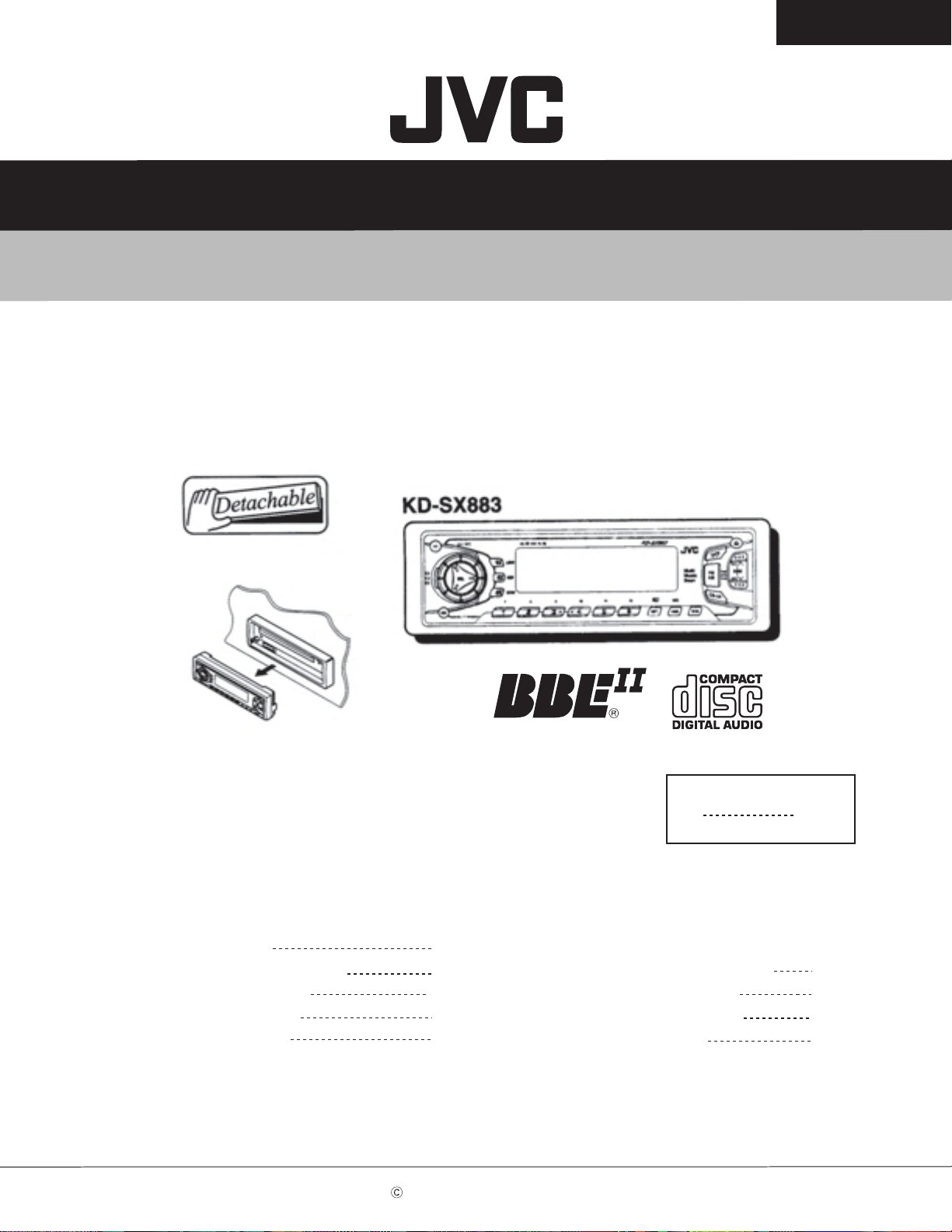
KD-SX883
KD-SX883
KD-SX883
Contents
Safety precaution
Preventing static electricity
Location of main parts
Disassembly method
Adjustment method
COPYRIGHT 2002 VICTOR COMPANY OF JAPAN, LTD.
1-2
1-3
1-4
1-5
1-10
Area Suffix
UF China
Flow of functional
operation unit TOC read
Maintenance of laser pickup
Replacement of laser pickup
Description of major ICs
1-11
1-13
1-13
1-14~28
No.49765
Nov. 2002
1-1
Page 2
KD-SX883
Safety precaution
!
!
Burrs formed during molding may be left over on some parts of the chassis. Therefore,
pay attention to such burrs in the case of preforming repair of this system.
Please use enough caution not to see the beam directly or touch it in case of an
adjustment or operation check.
1-2
Page 3
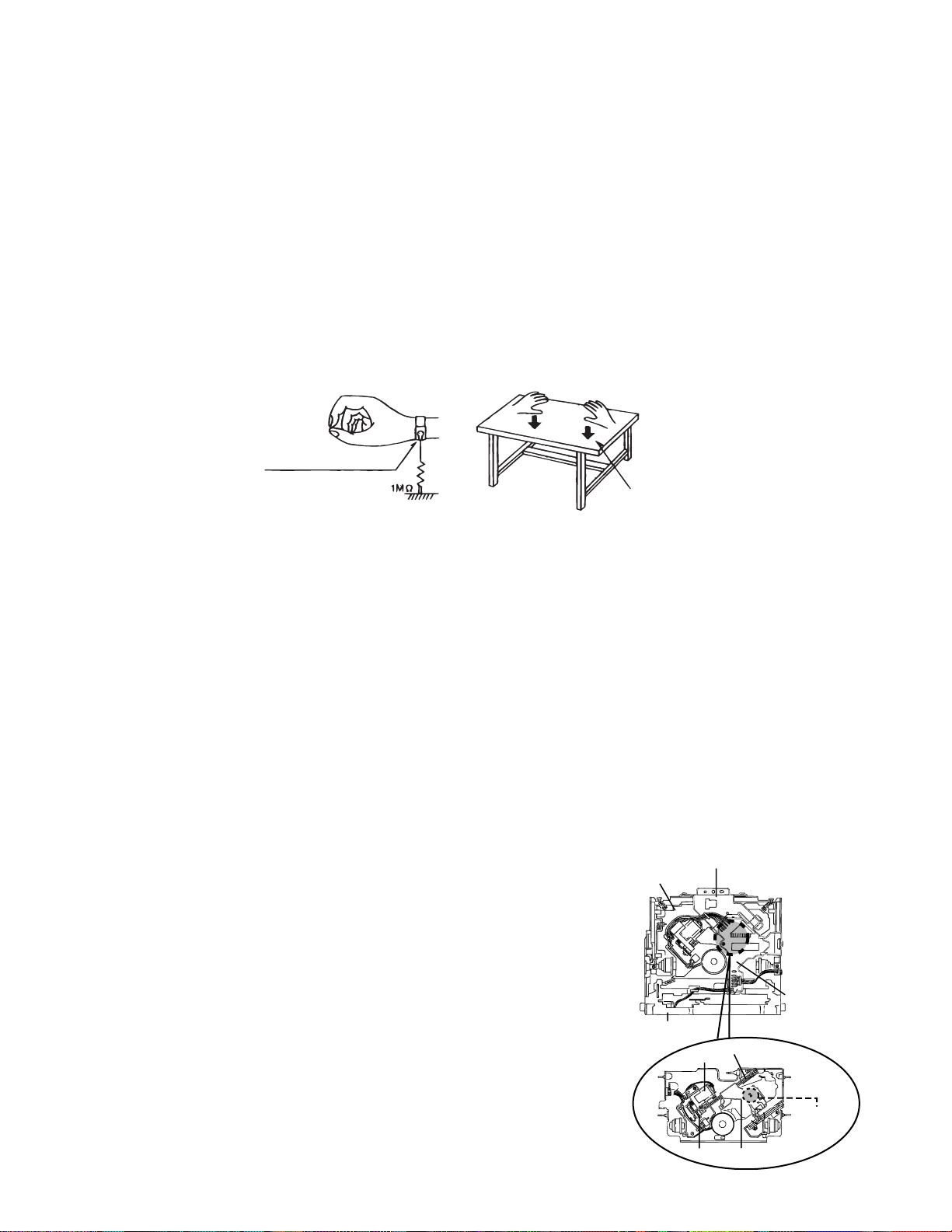
Preventing static electricity
KD-SX883
1.Grounding to prevent damage by static electricity
Electrostatic discharge (ESD), which occurs when static electricity stored in the body, fabric, etc. is discharged,
can destroy the laser diode in the traverse unit (optical pickup). Take care to prevent this when performing repairs.
2.About the earth processing for the destruction prevention by static electricity
Static electricity in the work area can destroy the optical pickup (laser diode) in devices such as CD players.
Be careful to use proper grounding in the area where repairs are being performed.
2-1 Ground the workbench
Ground the workbench by laying conductive material (such as a conductive sheet) or an iron plate over
it before placing the traverse unit (optical pickup) on it.
2-2 Ground yourself
Use an anti-static wrist strap to release any static electricity built up in your body.
(caption)
Anti-static wrist strap
Conductive material
(conductive sheet) or iron plate
3. Handling the optical pickup
1. In order to maintain quality during transport and before installation, both sides of the laser diode on the
replacement optical pickup are shorted. After replacement, return the shorted parts to their original condition.
(Refer to the text.)
2. Do not use a tester to check the condition of the laser diode in the optical pickup. The tester's internal power
source can easily destroy the laser diode.
4.Handling the traverse unit (optical pickup)
1. Do not subject the traverse unit (optical pickup) to strong shocks, as it is a sensitive, complex unit.
2. Cut off the shorted part of the flexible cable using nippers, etc. after replacing the optical pickup. For specific
details, refer to the replacement procedure in the text. Remove the anti-static pin when replacing the traverse
unit. Be careful not to take too long a time when attaching it to the connector.
3. Handle the flexible cable carefully as it may break when subjected to strong force.
4. It is not possible to adjust the semi-fixed resistor that adjusts the laser power. Do not turn it
CD mechanism ass’y
Damper bracket
Attention when traverse unit is decomposed
*Please refer to "Disassembly method" in the text for pick-up and how to
detach the substrate.
1.Solder is put up before the card wire is removed from connector on
the CD substrate as shown in Figure.
(When the wire is removed without putting up solder, the CD pick-up
assembly might destroy.)
2.Please remove solder after connecting the card wire with
when you install picking up in the substrate.
Front bracket
Feed motor ass’y
FD screw
CD mechanism
control board
FD gear
Soldering
Pickup unit
1-3
Page 4
KD-SX883
Location of main parts
Control unit
Display
SEL
Front PCB
Main unit
CD mechanism
Main board
16 pin connector
Power IC
Loading motor
Changer control
connector
Connector to front PCB
Antenna
jack
RCA jack
Main board assemb
Tuner
pack
ly
1-4
Damper
Optical
pick up unit
Mechanism relay board
Damper
Spindle motor
Damper
Feed motor
Page 5
KD-SX883
Disassembly method
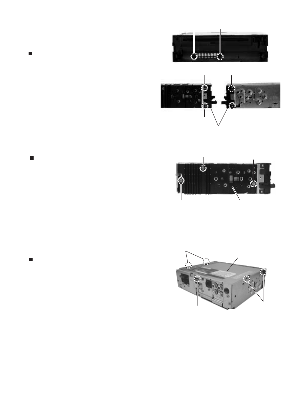
Removing the front chassis (See Fig.1)
1. Remove two screws A and insert a screwdriver to the
joints a on the side of the front chassis and two joints b
on the right side, then detach the front chassis toward the
front side.
Removing the heat sink (See Fig.2 )
1. Remove the three screws B attaching the heat sink on
the left side of the body, and remove the heat sink.
A
a
a
Front chassis
Fig.1
B
A
b
b
B
Removing the bottom cover (See Fig.3 )
1.2.Turn the body upside down.
Insert a screwdriver to the two joints c and two joints d on
both sides of the body and the joint e on the back of the
body, then detach the bottom cover from the body.
B
Heat sink
Fig.2
c
Regulator board
e
Fig. 3
d
1-5
Page 6
KD-SX883
Removing the main amplifier board assembly
(See Fig.4 and 5)
Remove the front chassis.
1.
Remove the bottom cover.
2.
Remove the two screws C attaching the main amplifier
3.
board assembly on the bottom of the body.
Remove the three screws D attaching the main amplifier
4.
board assembly on the back of the body.
Disconnect connector CN501 on the main amplifier board
5.
assembly from the CD mechanism assembly.
Main amplifier board
C
D
CN501
C
Fig.4
D
Fig. 5
Removing the CD mechanism assembly
Fig.6 )
(See
Remove the front chassis.
1.
Remove the bottom cover.
2.
Remove the main amplifier board assembly.
3.
Remove the three screws E attaching the CD mechanism
4.
assembly from the top cover.
Removing the control switch board
Fig.7 and 8 )
(See
1.
Remove the front chassis.
2.
Remove the four screws F attaching the rear cover on the
back of the front panel unit.
Remove the control switch board from the front panel
3.
unit.
CD mechanism assembly
Top cover
E
F
F
Control switch board
Fig. 6
Fig. 7
E
E
F
F
1-6
Fig. 8
Page 7
KD-SX883
<CD mechanism section>
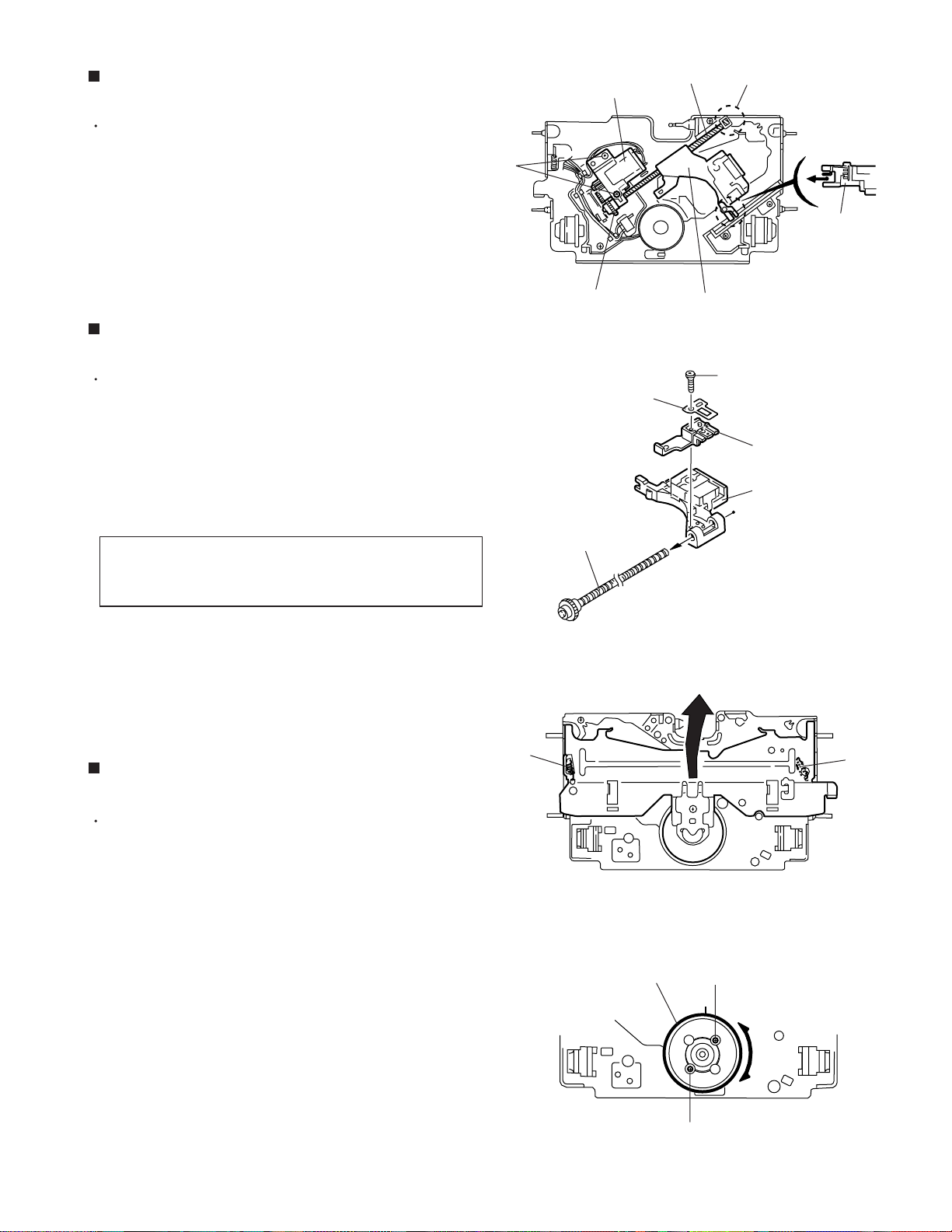
Removing the CD mechanism control
board (See Fig.1 and 2)
1.
Unsolder the part a and b on the CD mechanism
control board.
2.
Remove the stator fixing the CD mechanism control
board and the damper bracket (To remove the stator
smoothly, pick up the center part).
3.
Remove the screw A attaching the CD mechanism
control board.
4.
Remove the CD mechanism control board in the
direction of the arrow while releasing it from the two
damper bracket slots d and the front bracket slot e.
5.
Disconnect the flexible wire from connector on the
pickup unit.
ATTENTION:
Turn the FD gear in the direction of the
arrow to move the entire pickup unit to
the appropriate position where the
flexible wire of the CD mechanism unit
can be disconnected easily.
(Refer to Fig.2)
CD mechanism assembly
D
h
Front bracket
Pickup unit
Damper bracket
D
A
Fig.1
e
b
Flexible wire
a
h
c
D
d
CD mechanism
control board
Shift the lock
Removing the loading motor
(See Fig.3 to 5)
Prior to performing the following procedure, remove
the CD mechanism control board.
1.
Remove the two springs f attaching the CD
mechanism assembly and the front bracket.
2.
Remove the two screws B and the front bracket
while pulling the flame outward.
3.
Remove the belt and the screw C from the loading
motor.
Loading motor
C
FD gear
f
B
Loading motor
Pull outward
Fig.2
CD mechanism control board
f
B
Front bracket
Fig.3
Front bracket
Pull outward
Fig.5
Belt
Flame
Fig.4
1-7
Page 8
KD-SX883
Removing the CD mechanism assembly
(See Fig.1, 6 to 9)
Prior to performing the following procedure, remove
the CD mechanism control board and the front
bracket (loading motor).
1.
Remove the three screws D and the damper
bracket.
2.
Raise the both sides fix arms and move the fix plates
in the direction of the arrow to place the four shafts g
as shown in Fig.8 and 9.
3.
Remove the CD mechanism assembly and the two
springs h attaching the flame.
4.
Remove the two screws E and both sides rear
damper brackets from the dampers. Detach the CD
mechanism assembly from the left side to the right
side.
ATTENTION:
The CD mechanism assembly can be
removed if only the rear damper
bracket on the left side is removed.
CD mechanism
h
Front bracket
CD mechanism
D
Flame
assembly
D
assembly
h
D
Damper bracket
D
A
Fig.1
e
b
Damper bracket
D
Fig.6
a
h
c
D
d
CD mechanism
control board
h
Fix plate (L)
g
Fix arm (R)
D
Fig.7
Rear damper bracket
g
Fig.8
Rear damper bracket
E
Fix plate(R)
E
Fix arm (L)
Damper
1-8
Damper
g
g
Fig.9
Page 9
KD-SX883
Removing the feed motor assembly
(See Fig.10)
Prior to performing the following procedure, remove
the CD mechanism control board, the front bracket
(loading motor) and the CD mechanism assembly.
1.
Remove the two screws F and the feed motor
assembly.
Removing the pickup unit
(See Fig.10 and 11)
Prior to performing the following procedure, remove
the CD mechanism control board, the front bracket
(loading motor), the CD mechanism assembly and
the feed motor assembly.
1.
Detach the FD gear part of the pickup unit upward.
Then remove the pickup unit while pulling out the
part i of the FD screw.
Feed motor assembly
F
FD gear
Nut push spring plate
FD screw
Pickup unit
Fig.10
Part i
Part j
Pickup unit
G
Pickup mount nut
Pickup unit
ATTENTION:
2.
Remove the screw G attaching the nut push spring
plate and the pickup mount nut from the pickup unit.
Pull out the FD screw.
When reattaching the pickuap unit,
reattach the part j of the pickup unit,
then the part i of the FD screw.
Removing the spindle motor
(See Fig.12 and 13)
Prior to performing the following procedure, remove
the CD mechanism control board, the front bracket
(loading motor), the CD mechanism assembly and
the feed motor assembly.
1.
Turn up the CD mechanism assembly and remove
the two springs k on both sides of the clamper arms.
Open the clamper arm upward.
2.
Turn the turn table, and remove the two screws H
and the spindle motor.
FD screw
k
Spindle motor
Fig.11
k
Fig.12
H
H
Fig.13
1-9
Page 10
KD-SX883
Adjustment method
Test instruments required adjustment
1.Digital oscilloscope (100MHz)
2.AM Standard signal generator
3.FM Standard signal generator
4.Stereo modulator
5.Electric voltmeter
6.Digital tester
7.Tracking offset meter
8.Test Disc JVC : CTS-1000
9.Extension cable for check
EXTGS004-26P
Standard measuring conditions
Power supply voltage DC14.4V(10.5
Load impedance 4 (4 to 8 allowance)
Line-out Level / Impedance:
KD-SX975 : 4.0 V 20 k load (full scale)
KD-SX875 : 2.0 V 20 k load (full scale)
Standard volume position
Balance and Bass & Treble volume : Indication "0"
BBE:OFF
Frequency Band
FM
MW
Dummy load
Exclusive dummy load should be used for AM,and FM.
For FM dummy load, there is a loss of 6dB between SSG output
and antenna input. The loss of 6dB need not be considered
since direct reading of figures are applied in this working
standard.
–
16V)
1 – 3 87.5MHz – 108.0MHz
531kHz – 1602kHz
How to connect the extension cable for adjusting
EXTGS004-26P
1-10
Page 11
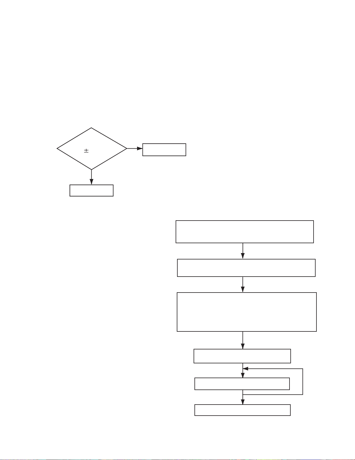
Flow of functional operation unit TOC read
Power ON
When the pickup correctly moves
to the inner area of the disc
Set Function CD
KD-SX883
When the laser diode correctly
emits
Microprocessor
commands
FMO
TC9462"53"
FEED MOTOR
+TERMINAL
IC581" 6 "
REST SW
When correctly focused
FEO
TA2109
14
Focus Servo Loop ON
$83
$82
$81
5V
Hi-Z
0V
6V
4V
2V
OFF
ON
Pickup feed to the inner area
2.2V
RF signal eye-pattern
remains closed
RF signal eye-pattern
opens
Disc inserted
YES
Laser emitted
Focus search
Disc rotates
Tracking loop closed
TOC readout
YES
Microprocessor
commands
SEL
TC9462
LD
CN501
57
1
"No disc"
display
When the disc correctly rotates
Microprocessor
commands
DMO
TC9462
Spindle
motor(-)
IC581" 5 "
$84 $86 $ A200
55
Acceleration Servo CLV
Rough
Servo
0.5 Sec 0.5 Sec
$84
5V
0V
4V
0V
5V
2.2V
0V
6V
3.2
2V
Jump to the first track
Play
Tracking Servo Loop ON
RF signal
Rough Servo Mode
CLV Servo Mode
(Program Area)
CLV Servo Mode
(Lead-In Area;
Digital: 0)
1-11
Page 12
KD-SX883
Feed section
Is the voltage output at
IC521 pin "53" 5V or 0V?
YES
Is 4V present at both
sides of the feed motor?
YES
NO YES NO
NO
Is the wiring for IC521
(90)~(100) correct?
NO
Is 6V or 2V present at
IC581 " 6 " and " 7 "?
NO
Is 5V present at IC581
pin "20"?
Check the vicinity of
IC521.
YES
Check the feed motor
connection wiring.
YES
Check CD 9V
and 5V.
Check the feed motor.
Focus section
When the lens is
moving:
4V
Does the S-search
waveform appear at
IC581 pins "8" and "9"?
Spindle section
Is the disk rotated?
YES
Does the RF signal
appear at TP1?
YES
Is the RF waveform at TP1
distorted?
YES
Proceed to the Tracking
section
Check IC581.
NO
YES
NO
NO
NO
Check the circuits in
the vicinity of IC501
pins "8","9"and"15".
Check the pickup and
its connections.
Is 4V present at IC581
pins "4" and "5"?
Check the spindle motor
and its wiring
Check the circuits in the
vicinity of IC501 "19"~
"24" or the pickup
YES
YES
NO
Is 4V present at IC521
pins "55" ?
Check the vicinity of
IC581.
NO
YES
Check IC501 and
IC521.
Tracking section
When the disc is rotated
Is the tracking error signal
output at IC501 "12"?
Check IC521.
1-12
at first:
Approx. 1.2V
YES
YES YES
Check the circuit in the
vicinity of IC501 pins
"2"~"12".
Check the pickup and
its connections.
Page 13
Maintenance of laser pickup
(1) Cleaning the pick up lens
Before you replace the pick up,please try to
clean the lens with a alcohol soaked cotton
swab.
(2) Life of the laser diode
When the life of the laser diode has expired,
the following symptoms will appear.
(1) The level of RF output (EFM output:ampli tude of eye pattern) will be low.
KD-SX883
Is RF output
1.3 0.4Vp-p?
YES
O.K
(3) Semi-fixed resistor on the APC PC board
The semi-fixed resistor on the APC printed
circuit board which is attached to the pickup
is used to adjust the laser power. Since this
adjustment should be performed to match the
characteristics of the whole optical block,
do not touch the semi-fixed resistor.
If the laser power is lower than the specified
value, the laser diode is almost worn out, and
the laser pickup should be replaced.
If the semi-fixed resistor is adjusted while
the pickup is functioning normally, the laser
pickup may be damaged due to excessive current.
NO
Replace it.
Replacement of laser pickup
Turn off the power switch and,disconnect the
power cord.
Replace the pickup with a normal one.(Refer
to "Pickup Removal" on the previous page)
Plug the power cord in, and turn the power on.
At this time, check that the laser emits for
about 3seconds and the objective lens moves
up and down.
Note: Do not observe the laser beam directly.
Play a disc.
Check the eye-pattern at TP1.
Finish.
1-13
Page 14
KD-SX883
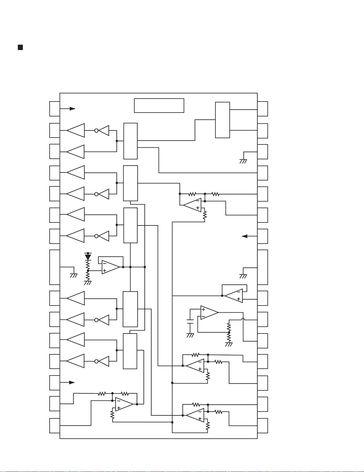
Description of major ICs
LA6567H-X (IC581) : CD driver
1.Pin layout & Block diagram
VCC2
V05-
V05+
V04+
V04-
V03+
V03-
FR
1
2
3
4
5
6
7
FR
CH 3,4,5
Power supply
CH5
CH4
CH3
Thermal shutdown
Output control
Level shiftLevel shiftLevel shiftLevel shift
Input
22K 11K
Signal system power supply
28
27
26
25
24
23
22
FR
REV
FWD
S-GND
VCONT
VIN4
VIN4G
VCC-S
FR
V02+
V02-
V01+
V01-
VCC1
VIN1
VIN1G
1-14
8
9
10
11
12
13
14
CH2
CH1
CH1,2
Power supply
11K
22K
5VREG(PNPTr
The outside putting)
22K
11K
22K
11K
21
20
19
18
17
16
15
VREF-IN
REG-OUT
REG-IN
VIN3G
VIN3
VIN2G
VIN2
Page 15
KD-SX883
2. Pin function
Pin no. Symbol
1
2
3
4
5
6
7
8
9
10
11
12
13
14
15
16
17
18
19
20
21
22
23
24
25
26
27
VCC2
V05V05+
V04+
V04V03+
V03V02+
V02V01+
V01-
VCC1
VIN1
VIN1G
VIN2
VIN2G
VIN3
VIN3G
REG-IN
REG-OUT
VREF-IN
VCC-S
VIN4G
VIN4
VCONT
S-GND
FWD
LA6567H-X(2/2)
Function
CH3,4,5 Power supply( It is short with VCC1,VCC-S)
Loading output(-)
Loading terminal (+)
CH4 Output terminal(+)
CH4 Output terminal(-)
CH3 Output terminal(+)
CH3 Output terminal(-)
CH2 Output terminal(+)
CH2 Output terminal(-)
CH1 Output terminal(+)
CH1 Output terminal(-)
CH1,2(BTL) Power supply(It is short with VCC-S,VCC2)
CH1 Input terminal
CH1 Input terminal(For gain adjustment)
CH2 Input terminal
CH2 Input terminal(For gain adjustment)
CH3 Input terminal
CH3 Input terminal(For gain adjustment)
Regulator terminal(Outside putting PNP base)
Regulator terminal(Outside putting PNP collector)
Standard voltage input terminal
Signal system power supply(It is short with VCC1,VCC2)
CH4 Input terminal(For gain adjustment)
CH4 Input terminal
5CH(VLO) Output voltage set terminal
Signal system GND
5CH(VLO)Signal output switch terminal(FWD),Input of logic of loading part
28
REV
5CH(VLO)Signal output switch terminal(REV),
Input of logic of loading part
Frame(FR)at the center becomes system GND.
Please be short-circuited on the outside and use the terminal of the power supply system
and three teminals of VCC-S, VCC1,VCC2.
1-15
Page 16

KD-SX883
LC75873NW (IC601) : LCD driver
1.Block diagram
COM3
COM2
COM1
S68
S67
S5
S4/P4
S3/P3
S2/P2
S1/P1
VDD1
VDD2
INH
OSC
VDD
VSS
COMMOM
DRIVER
CLOCK
GENERATOR
SEGMENT DRIVER
SHIFT REGISTER
ADDRESS
DETECTOR
2.Pin functions
Pin No. Symbol Description
1~66
67~69
70
71
S3~S68
COM1~3
VDD
VDD1
I/O
Segment Output.
O
Common Driver Output.
O
Power Supply Connection.
-
Used for applying the LCD drive 2/3 bias voltage externally.
I
Must be connected to VDD2 when a 1/2 bias drive scheme in used.
72
VDD2
Used for applying the LCD drive 1/3 bias voltage externally.
I
Must be connected to VDD1 when a 1/2 bias drive scheme in used.
73
74
VSS
OSC
Power supply connection.
-
Oscillator connection. An oscillator circuit is formed by connecting an
I/O
external resistor and capacitor to this pin.
75
76
77
78
79
80
INH
CE
CLOCK
DI
DIMMER
NC
Display off control input.
I
Chip enable input.
I
Synchronization clock input.
I
Serial data input.
I
DIMMER Control signal output.
O
Non connect.
-
1-16
Page 17
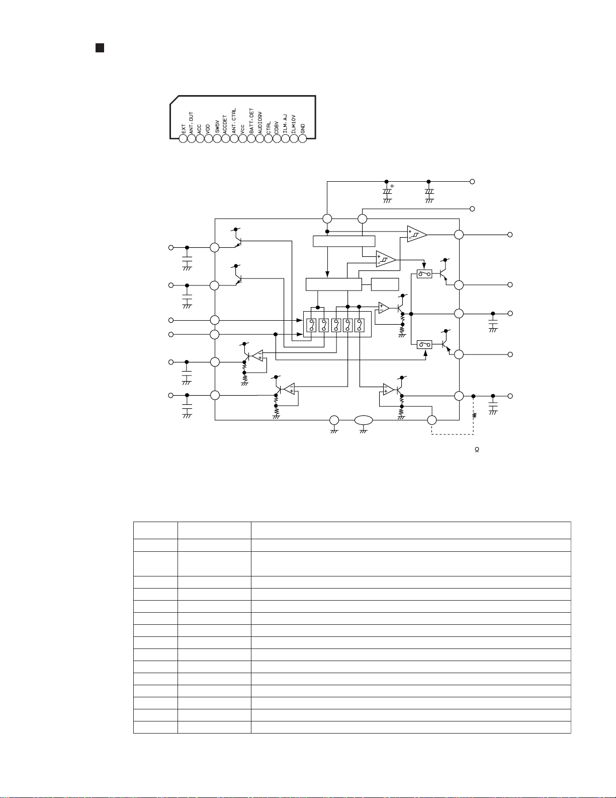
HA13164A (IC961) : Regulator
1.Pin layout
123456789101112131415
KD-SX883
2.Block diagram
ANT OUT
C3
0.1u
EXT OUT
C4
0.1u
ANT CTRL
CTRL
CD OUT
C5
0.1u
AUDIO OUT
C6
10u
11
12
10
BATT.DET OUT
9
COMPOUT
6
VDD OUT
4
SW5VOUT
5
14
UNIT R:
+B
ACC
ILMOUT
R1
C7
0.1u
C8
0.1u
C1
100u
VCC ACC
8
2
1
7
Surge Protector
BIAS TSD
15
3
TA B
note1) TAB (header of IC)
ILM AJGND GND
connected to GND
13
C2
0.1u
C:F
3.Pin function
Pin No. Symbol Function
1
2
EXTOUT
ANTOUT
Output voltage is VCC-1 V when M or H level applied to CTRL pin.
Output voltage is VCC-1 V when M or H level to CTRL pin and H level
to ANT-CTRL.
3
4
5
6
7
8
9
10
11
12
13
14
15
ACCIN
VDDOUT
SW5VOUT
COMPOUT
ANT CTRL
VCC
BATT DET
AUDIO OUT
CTRL
CD OUT
ILM AJ
ILM OUT
GND
Connected to ACC.
Regular 5.7V.
Output voltage is 5V when M or H level applied to CTRL pin.
Output for ACC detector.
L:ANT output OFF , H:ANT output ON
Connected to VCC.
Low battery detect.
Output voltage is 9V when M or H level applied to CTRL pin.
L:BIAS OFF, M:BIAS ON, H:CD ON
Output voltage is 8V when H level applied to CTRL pin.
Adjustment pin for ILM output voltage.
Output voltage is 10V when M or H level applied to CTRL pin.
Connected to GND.
1-17
Page 18

KD-SX883
F
LA4743K (IC351) : Power amp
1.Block diagram
IN 1
TA B
IN 2
+
0.22 F
+
0.22 F
11
1
12
Vcc 1/2 Vcc 3/4
6 20
-
+
Protective
circuit
-
+
2200 F 0.022
+
9
7
+
OUT 1+
OUT 1-
PWR GND1
8
+
OUT 2+
5
-
OUT 2-
3
PWR GND2
2
ST BY
R.F
47 F
IN 3
PRE GND
IN 4
+5V
ST ON
+
0.22 F
N.C
+
0.22 F
4
Stand by
Switch
Mute
10
+
Ripple
Filter
Mute
22
circuit
3.3 F
+
15
-
+
-
17
19
10K
+
OUT 3+
OUT 3-
Low Level
Mute ON
25
18
21
23
PWR GND3
OUT 4+
OUT 4-
13
14
Protective
circuit
-
+
+
-
1-18
ON TIME C
22 F
Muting &
16
+
ON Time Control
Circuit
PWR GND4
24
Page 19

2.Terminal layout
KD-SX883
3.Pin function
1
2
3
4
5
6
7
8
9
10
11
12
13
14
15
16
17
18
19
20
21
22
23
24
25
SymbolPin No. Function
TA B
GND
OUTRRSTBY
OUTRR+
VCC1/2
OUTRFGND
OUTRF+
RIPPLE
INRF
INRR
SGND
INLR
INLF
ONTIME
OUTLF+
GND
OUTLFVCC3/4
OUTLR+
MUTE
OUTLRGND
NC
Header of IC
Power GND
Outpur(-) for front Rch
Stand by input
Output (+) for front Rch
Power input
Output (-) for rear Rch
Power GND
Output (+) for rear Rch
Ripple filter
Rear Rch input
Front Rch input
Signal GND
Front Lch input
Rear Lch input
Power on time control
Output (+) for rear Lch
Power GND
Output (-) for rear Lch
Power input
Output (+) for front
Muting control input
Output (-) for front
Power GND
Non connection
LA4743B
1-19
Page 20

KD-SX883
TA2109F-X (IC501) : RF amp.
1. Pin layout
24 13
112
2. Block diagram
SBAD
13
FEO
14
10pF
FEN
15
10k ohm
VRO
16
21k ohm
20k ohm
RFRP
17
RFIS
18
20k ohm
RFGO
19
50k ohm
36pF
7.96k ohm
50uA
20k ohm
15k ohm 30k ohm
15k ohm
20uA
10k ohm
21k ohm
12k ohm
12k ohm
PEAK
BOTTOM
10k ohm
10k ohm
30k ohm
21k ohm 29k ohm
24k ohm 24k ohm
180k ohm
1.74k ohm
20pF
65uA
10k ohm
47k ohm
SW3
13k ohm
7.67k ohm
3 STATE
DET.
SW1
1k ohm
SW2
680 ohm
2.12k ohm
20pF
LDC
TEO
TEN
2VRO
TEB
SEL
LDO
MDI
12
11
10
9
8
7
6
3. Pin function
Pin
Symbol I/O
No.
Vcc
FNI
FPI
TPI
TNI
MDI
LDO
SEL
TEB
TEN
TEO
I
I
I
I
I
O
I
I
O
I
O
1
2
3
4
5
6
7
8
9
10
11
12
2VRO
RFGC
20
AGCI
21
re=130 ohm
RFO
22
GND
23
RFN
24
23.5k ohm
3.3k ohm
12k ohm
1.53k ohm
3.3k ohm
Pin function
Power supply input terminal
Main beam I-V amp input terminal
Main beam I-V amp input terminal
Sub beam I-v input terminal
Sub beam I-V input terminal
Monitor photo diode amp input terminal
Laser diode amp output terminal
Laser diode control signal input terminal
T. error balance adj. signal input terminal
Reference voltage output terminal
TE amp negative input terminal
TE error signal output terminal
180k ohm
40pF
180k ohm
Pin
No.
13
14
15
16
17
18
19
20
21
22
23
24
180k ohm
20pF
60k ohm
60k ohm
40pF
Symbol I/O
SBAD
FEO
O
O
FEN
VRO
O
RFRP
O
RFIS
RFGO
O
RFGC
AGCI
RFO
O
GND
RFN
TNI
TPI
FPI
FNI
Vcc
5
4
3
2
1
I-I
I-I
20k ohm
20k ohm
20k ohm
20k ohm
Pin function
Sub beam adder signal output terminal
Focus error signal output terminal
FE amp negative input terminal
I
Reference voltage (VREF) output terminal
Track count signal output terminal
RFRP detect circuit input terminal
I
RF gain signal output terminal
RF amplitude adj. control signal input terminal
I
RF signal amplitude adj. amp input terminal
I
RF signal output terminal
Ground terminal
RF amp negative input terminal
I
1-20
Page 21

UPD178078GF-543 (IC701) : SYSTEM CPU
KD-SX883
1.Terminal layout
2.Block diagram
TO0/VTR-CONT
TI00/POWER
TI01/CD-ON
TI50/MUTE
TO50/NC
TI51/STAGE
TO51/NC
SI0/SB0/SDA0/NC
SO0/SB1/SDA1/VOL-DA
SCK0/SCL/VOL-CLK
SI1/JBUS-SI
SO1/JBUS-SO
SCK1/JBUS-SCK
STB/NC
BUSY/NC
SI3/NC
SO3/LCD-DA
SCK3/SCL/LCD-CLK
TXD0/LM1
RXD0/LM0
INTP0/NC
INTP7/NC
BEEP0/BUZZER
BUZ/NC
RESET
X1
X2
V
DD
PORT
GNDPORT
DD
V
VM45/VTR-LOGIC
REGOSC
REGCPU
GND0
GND1
16-bit TIMER/
EVENT COUNTER
8-bit TIMER/
EVENT COUNTER 0
8-bit TIMER/
EVENT COUNTER 1
WATCHDOG TIMER
BASIC TIMER
SERIAL
INTERFACE 0
SERIAL
INTERFACE 1
SERIAL
INTERFACE 3
8
INTERRUPT
CONTROL
BUZER OUTPUT
SYSTEM
CONTROL
VOLTAGE
REGULATOR
1
~
30
UART0
100 ~ 81
31 ~ 50
80
~
51
78k/0
CPU
CPRE
RAM
PD178078
:3Kbyte
PD178076
:2Kbyte
RESET
CPU
PERIPHERAL
OSC
V
V
CPU
ROM
PD178078
:60Kbyte
PD178076
:48Kbyte
PORT 0
PORT 1
PORT 2
PORT 3
PORT 4
PORT 5
PORT 6
PORT 7
PORT10
PORT 12
PORT 13
A/D
CONVERTER
FREQUENCY
COUNTER
PLL
PLL
VOLTAGE
REGULATOR
NC,JBUS-INT,SW1,
8
REMOCON,PS1,PS2,
DETACH,NC
KEY0,KEY1,KEY2,LEVEL,
8
SM,OPEN.NC,
JBUS-SI,JBUS-SO,
8
JBUS-SCK,NC,VOL-DA,
VOL-CLK
VTR-LOGIC,VTR-CONT,
8
POWER,CD-ON,MUTE,
NC.BUZZER.NC
8
NC
NC,LCD-CE,SW2,SW3,
8
SW4,RST-SW,ENC1,ENC2
MONO,SEEK/STOP,
8
FM/AM.DIM IN.ANTENNA.
TEL MUTING.STAGE1.STAGE2
NC,LCD-DA,LCD-CLK,
8
JBUS-/O,LM0,LM1,BUCK,
CCE
3
SD/ST,NC,IFC
5
BUS0,BUS1,BUS2,BUS3,
RST
8
NC
AN10/KEY0
8
AN17/NC
AV
DD
AV
SS
AMIFC/NC
FMIFC/IFC
EO0
EO1
VCOL
VCOH
DD
PLL
V
GNDPLL
IC
GND2
1-21
Page 22

KD-SX883
3.Pin function
Pin
NO.
1
2
3
4
5
6
7
8
9
10
11
12
13
14
15
16
17
18
19
20
21
22
23
24
25
26
27
28
29
30
31
32
33
34
35
36
37
38
39
40
41
42
43
44
45
46
47
48
49
50
NC
JBUS-INT
JBUS-SI
JBUS-SO
JBUS-SCK
NC
NC
NC
VOL-DA
VOL-CLK
NC
LCD-DA
LCD-CLK
JBUS-I/O
NC
LCD-CE
SW2
SW3
SW4
RST-SW
ENC1
ENC2
KEY0
KEY1
KEY2
LEVEL
AVDD
SM
OPEN
NC
NC
AVSS
REGCPU
VDD
REGOSC
X2
X1
GND
SD/ST
GND2
NC
IFC
VDDPLL
OSC-INPUT
NC
GNDPLL
AME0
FME0
ICVPP
RESET
UPD178078GF(1/2)
I/OSymbol
-
Non connection
I
JVC BUS COMMUNICATION LINE
I
JVC BUS COMMUNICATION LINE
O
JVC BUS COMMUNICATION LINE
O
JVC BUS COMMUNICATION LINE
-
Non connection
-
Non connection
-
Non connection
O
VOL IC COMMUNICATION LINE
O
VOL IC COMMUNICATION LINE
-
Non connection
O
CD DRIVER COMMUNICATION LINE
O
LCD DRIVER COMMUNICATION LINE
O
JVC BUS OUTPUT SELECT
-
Non connection
O
LCD DRIVER COMMUNICATION LINE
I
CD MECHA SW
I
CD MECHA SW
I
CD MECHA SW
I
TRAVERSE MECHA REST SW
I
ENCODER INPUT
I
ENCORDER INPUT
I
KEY INPUT
I
KEY INPUT
I
KEY INPUT
I
AUDIO LEVEL INPUT
-
-
I
SIGNAL LEVEL METER INPUT
I
DOOR OPEN DATECTION
-
Non connection
-
-
-
-
-
-
-
-
-
SYSTEM CLOCK
I
SYSTEM CLOCK
-
-
-
-
I
STATION DETECTOR & STERO IND
-
Non connection
-
IF COUNT INPUT
I
-
-
FM,AM OSC INPUT
I
Non connection
-
-
-
PLL ERROR OUTPUT FOR AM
O
PLL ERROR OUTPUT FOR FM
O
SETTING TO WRITE FOR FLASH
-
SYSTEM RESET
I
SYSTEM RESET
FUNCTION
1-22
Page 23

Pin
NO.
51
52
53
54
55
56
57
58
59
60
61
62
63
64
65
66
67
68
69
70
71
72
73
74
75
76
77
78
79
80
81
82
83
84
85
86
87
88
89
90
91
92
93
94
95
96
97
98
99
100
SW1
REMOCON
VTR-LOGIC
VTR-CONT
POWER
CD-ON
MUTE
NC
BUZZER
NC
NC
NC
NC
NC
NC
NC
NC
NC
LM0
LM1
BUCK
CCE
BUS0
BUS1
BUS2
BUS3
RST
PS1
PS2
DETACH
NC
GND1
MONO
SEEK/STOP
FM/AM
DIMIN
ANT
TEL MUTE
STAGE1
STAGE2
NC
NC
NC
NC
NC
NC
NC
DIMMER
VDDPORT
GNDPORT
I/OSymbol
I
I
-
O
O
O
-
I
-
-
-
-
-
-
-
-
O
O
O
O
I/O
I/O
I/O
I/O
O
I
I
I
-
O
O
O
I
O
I
-
-
-
-
-
-
-
-
O
-
KD-SX883
UPD178078GF(2/2)
FUNCTION
CD MECHA SW
REMOCON INPUT
Non connection
Non connection
POWER CONT.
CD POWER CONT.
MUTE CONT
Non connection
BEEP FOR SW OPERATION
Non connection
Non connection
Non connection
Non connection
Non connection
Non connection
Non connection
Non connection
Non connection
CD MECHA DRIVER CONT.
CD MECHA DRIVER CONT.
CD LSI COMMUNICATION LINE
CD LSI COMMUNICATION LINE
CD LSI COMMUNICATION LINE
CD LSI COMMUNICATION LINE
CD LSI COMMUNICATION LINE
CD LSI COMMUNICATION LINE
CD LSI COMMUNICATION LINE
ACC DETECTION INPUT
MEMORY DETECTION
DETACH DETECTION
Non connection
MONO BY FORCE
SWITCHING SEEK & STOP
BAND SW
OUTPUT L
ILM CONTROL
ANT COTROL
TEL MUTE IN
Non connection
Non connection
Non connection
Non connection
Non connection
Non connection
Non connection
Non connection
Non connection
DIMMER CONTROL
-
-
1-23
Page 24

KD-SX883
TC9462F (IC521) : DSP
1. Pin layout & Block diagram
RST
DD
XV
80
79
81DV
SR
82RO
83DV
DD
84DVR
85LO
86DV
SL
87TEST1
88TEST2
89TEST3
90BUS0
91BUS1
92BUS2
93BUS3
94V
DD
95V
SS
96BUCK
97CCE
98TEST4
99TSMOD
100
1 2 3
TEST0
XO78XI
LPF
HSO
Micon
interface
UHSO
SS
XV
77
4 5
EMPH
76
1bit
DAC
DD
V
75
PXO
SS
PXI
V
74
73
Clock
generator
Correction
circuit
Audio out
circuit
6
7 8 9 10 11 12 13
SS
V
BCK
LRCK
AOUT
TESIO1
72
DOUT
71
TESIN
MBOV
DACT
69
70
Address circuit
16KRAM
Digital out
IPF
CKSE
SBOK
DMOUT
68
CLCK
IO3
IO265IO164IO063V
67
66
ROM
Automatic adjustment
RAM
Synchronous
guarantee
EFM decode
Sub code
decoder
14 15
16 17 18 19 20 21 22
SS
DD
V
V
DATA
SFSY
SS
DD
V
61
62
Servo
control
Digital equalizer
circuit
CLV servo
SBSY
SPCK
FLGD60FLGC59FLGB58FLGA57SEL562V
PWM D/A
A/D
Status
TMAX
23 24 25
DD
COFS
MONIT
V
TESIO0
SPDA
REF
DMO54FVO53FMO52TEBC51RFGC
55
+
-
Data
slicer
VCO
PLL
26
27 28
REF
P2V
HSSW
ZDET
PDO
50 V
REF
49 TRO
48 FOO
TEZI
TMAXS
30
TMAX
47
46 TEI
45 TSIN
44 SBAD
43 FEI
42 RFRP
41 RFZI
40 RFCT
39 AV
DD
38 RFI
37 SLCO
36 AV
SS
35 VCOF
34 VCOREF
33 PV
REF
32 LPFO
31 LPFN
+
-
+
-
+
-
29
2. Pin function
PIN No.
1
2
3
4
5
6
7
8
9
10
11
12
13
14
15
16
17
18
19
20
21
22
23
24
25 P2V
SYMBOL
TEST0
HSO
UHSO
EMPH
LRCK
V
SS
BCK
AOUT
DOUT
MBOV
IPF
SBOK
CLCK
V
DD
V
SS
DATA
SFSY
SBSY
SPCK
SADA
COFS
MONIT
V
DD
TESIO0
REF
FUNCTIONAL DESCRIPTION
I/O
Test mode terminal.Normally, Keep at open.
I
Playback speed mode flag output terminal.
UHSO
HSO
O
H
H
L
O
Subcode Q data emphasis flag output terminal.Emphasis ON at "H" level and OFF at "L"
O
level.The output polarity can invert by command.
Channel clock output terminal.(44.1khz)L-ch at "L" level and R-ch at "H" level. the output
O
polarity can invert by command.
Digital GND terminal.
-O
Bit clock output terminal.(1.4112MHz)
Audio data output terminal.
O
Digital data output terminal.
O
Buffer memory over signal output terminal. Over at "H" level.
O
Correction flag output terminal. At "H" level,AOUT output is made to correction
O
impossibility by C
Subcode Q data CRCC check adjusting result output terminal.
O
The adjusting result is OK at "H" level.
Subcode P W data readout clock input/output terminal.
I/O
This terminal can select by command bit.
--
Digital power supply voltage terminal.
--
Digital GND terminal.
O
Subcode P W data output terminal.
O
Play-back frame sync signal output terminal.
O
Subcode block sync signal output terminal.
O
Processor status signal readout clock output terminal.
O
Processor status signal output terminal.
O
Correction frame clock output terminal. (7.35kHz)
Internal signal (DSP internal flag and PLL clock) output terminal.Selected by command.
O
This terminal output the text data with serial by command.
--
Digital power supply voltage terminal.
Test input/output terminal.Normally,keep at "L" level.
I
The terminal that inputted the clock for read of text data by command.
--
PLL double reference voltage supply terminal.
L
PLAYBACK SPEED
H
L
H
L
2 correction processing.
Nomal
2 times
4 times
--
REMARKS
With pull-up resistor.
--
--
--
--
--
--
--
--
--
--
--
--
--
--
--
--
--
--
--
--
--
--
--
1-24
Page 25

Pin No.
26
27
28
29
30
Symbol
HSSW
ZDET
PDO
TMAXS
TMAX
I/O
2/4 times speed at "VREF" voltage.
O
1 bit DA converter zero detect flag output terminal.
O
Phase difference signal output terminal of EFM
O
Function Remarks
signal and PLCK signal.
TMAX detection result output terminal. Selected by
O
command bit (TMPS)
TMAX detection result output terminal. Selected by
O
command bit (TMPS)
DIFFERENCE RESULT TMAX OUTPUT
Longer than fixed freq. "P2VREF"
Shorter than fixed freq. "VSS"
Within the fixed freq. "Hiz"
KD-SX883
TC9462F(2/3)
2-state output
3-state output.
(P2VREF,PVREF,VSS)
3-state output.
(P2VREF,PVREF,VSS)
3-state output.
(P2VREF,HiZ,VSS)
-
(PVREF,HiZ)
31
32
33
34
35
36
37
38
39
40
41
42
43
44
45
46
47
48
49
50
51
52
53
54
55
56
57
58~61
62
63
64~67
68
69
70
LPFN
LPFO
PVREF
VCOREF
VCOF
AVSS
SLCO
RFI
AVDD
RFCT
RFZI
RFRP
FEI
SBAD
TSIN
TEI
TEZI
FOO
TRO
VREF
RFGC
TEBC
FMO
FVO
DMO
2VREF
SEL
FLGA~D
VDD
VSS
IO0~3
DMOUT
CKSE
DACT
LPF amplifier inverting terminal for PLL.
I
LPF amplifier output terminal for PLL.
O
PLL reference voltage supply terminal.
VCO center frequency reference level terminal. Normally,
I
keep at "PVREF" level.
VCO filter terminal.
O
Analog GND terminal.
Data slice level output terminal.
O
RF signal input terminal.
I
Analog power supply voltage terminal.
-
RFRP signal center level input terminal
I
RFRP zero cross input terminal
I
RF ripple signal input terminal
I
Focus error signal input terminal
I
Sub-beam adder signal input terminal
I
Test input terminal Normally, keep at "vref" level
I
Tracking error signal input terminal. Take in at tracking
I
servo ON.
Tracking error zero cross input terminal
I
Focus servo equalizer output terminal
O
Tracking servo equalizer output terminal
O
Analog reference voltage supply terminal
-
RF amplitude adjustment control signal output terminal
O
Tracking balance control signal output terminal
O
Feed equalizer output terminal
O
Speed error signal or feed search equalizer output
O
terminal
Disk equalizer output terminal
O
DSP, Synchronize to PXO)
Analog double reference voltage supply terminal
-
APC circuit ON/OFF indication signal output terminal
O
External flag output terminal for internal signal
O
Digital power supply voltage terminal
-
Digital GND terminal
-
General I/O terminal
I/O
This terminal control IO0~IO3 terminal
I
Normally, keep at open
I
DAC test mode terminal. Normally, keep at open
I
(PWM carrier=88.2kHz for
Analog input.
Analog output.
-
-
Analog output.
Analog output.
Analog input.
(Zin:selected by command)
Analog input
(Zin : 50k )
Analog input.
Analog input.
Analog input.
Analog input.
Analog input.
Analog input.
Analog input
Analog output.
(Zin :10k )
(2VREF AVSS)
3-state PWM signal
output.
(2VREF,VREF,VSS)
(PWM carrier
=88.2kHz)
3-state output.
(2VREF,VREF,VSS)
-
-
-
-
-
With pull-up resistor.
With pull-up resistor.
With pull-up resistor.
1-25
Page 26

KD-SX883
t
Pin No.
71
72
73
74
75
76
77
78
79
80
81
82
83
84
85
86
87~89
90~93
94
95
96
97
98
99
100
Symbol
TESIN
TESIO1
VSS
PXI
PXO
VDD
XVSS
XI
XO
XVDD
DVSR
RO
DVDD
DVR
LO
DVSL
TEST1~3
BUS0~3
VDD
VSS
BUCK
CCE
TEST4
TSMOD
RST
I/O
Test input terminal, Normally, keep at "L" level
I
Test input/output terminal. Normally, keep at "L" level
I
Digital GND terminal
Crystal oscillator connecting input terminal for DSP
I
Crystal oscillator connecting output terminal for DSP
O
Digital power supply voltage terminal
Oscillator GND terminal for system clock
Crystal oscillator connecting input terminal for system
I
Function Remarks
clock
Crystal oscillator connecting output terminal for system
O
clock
Oscillator power supply voltage terminal for system clock
Analog GND terminal for DA converter (Rch)
R channel data forward output terminal
O
Analog supply voltage terminal for DA converter
Reference voltage terminal for DA converter
L channel data forward output terminal
O
Analog GND terminal for DA converter (Lch)
Test mode terminal . Normal keep at open
I
Micon interface data input/output terminal
I/O
Digital power supply voltage terminal
Digital GND terminal
Micon interface clock input terminal
I
Command and data sending/receiving chip enable signal
I
input terminal
Test mode terminal. Normal, keep at open
I
Local test mode selection terminal
I
Reset signal input terminal. Reset at "L" level
I
TC9462F(3/3)
Analog input.
Analog input.
-
-
-
-
-
-
-
-
-
-
-
-
-
With piull-up resistor.
Schmit input.
With pull-up resistor.
-
Schmit input.
Schmit input.
With pull-up resistor.
With pull-up resistor.
With pull-up resistor.
RPM6938-SV4 (IC602) : Remote control receiver
AGC
AMP
I/V
conversion
PD
magnetic shield
1-26
BPF
for
trimming
circuit
Detector
Vcc
Comp
22k
ohm
Vcc
Rou
GND
Page 27

BD3860K (IC301) : E. volume
1.Terminal layout
33 23
KD-SX883
2.Bock diagram
GND FIL VCC SEL1
6 5 9 40 36 35 343328323130 2919 15 14
POWER
SUPPLY
A1
41
B1
42
C1
43
D1
44
INPUT
1
2
3
4
SELECTOR
A2
B2
C2
D2
34
44
1 11
INPUT
GAIN
0 18 dB
INPUT
GAIN
0 18 dB
22
12
VIN1 LOUD1 HF1 LF1 DET1 TIN1 TNF1 BNF1
MAIN
VOLUME
0 -40 dB
LOUDNESS
MAIN
VOLUME
0 -40 dB
LOUDNESS
LOW(f=50Hz) 6dB
PROCESS CONTROL +3 to 12dB
(f=10kHz)
LOGIC
LOW(f=50Hz) 6dB
PROCESS CONTROL +3 to 12dB
(f=10kHz)
TREBLE
-14 +14dB
TREBLE
-14 +14dB
-14 +14dB
-14 +14dB
BASS
BASS
BOUT1VCA1 MIX1 BBOUT1
FAD ER
CH1 FRONT
0 -5 dB
FAD ER
CH1 REAR
0 -5 dB
FAD ER
CH2 REAR
0 -5 dB
FAD ER
CH2 FRONT
0 -5 dB
13
12
10
11
7
8
OUTF1
OUTR1
SI
SC
OUTR2
OUTF2
3.Pin function
Pin
Symbol Function
No.
1
2
3
4
5
6
7
8
9
10
11
12
13
14
15
16
17
18
19
20
21
BBOUT2
22
A2
B2
C2
D2
FIL
GND
SI
SC
VCC
OUTR2
OUTF2
OUTR1
OUTF1
BOUT1
BNF1
BOUT2
BNF2
TNF2
TNF1
TIN2
MIX2
CH2 Input Pin A
CH2 Input Pin B
CH2 Input Pin C
CH2 Input Pin D
1/2 VCC Pin
Ground Pin
Serial Data Receiving Pin
Serial Clock Receiving Pin
Power Supply Pin
CH2 Rear Output Pin
CH2 Front Output Pin
CH1 Rear Output Pin
CH1 Front Output Pin
CH1 Bass Filter Setting Pin
CH1 Bass Filter Setting Pin
CH2 Bass Filter Setting Pin
CH2 Bass Filter Setting Pin
CH2 treble Filter Setting Pin
CH1 treble Filter Setting Pin
CH2 treble Input Pin
CH2 BBE II Signal Output Pin
CH2 Output MIX Amplifier
Inverse Input Pin
39 38 37 25 24 26 23 22 21 20 18 17 16
Pin
Symbol Function
No.
23
24
25
26
27
28
29
30
BBOUT1
31
32
33
34
35
LOUD1
36
37
LOUD2
38
39
40
41
42
43
44
VCA2
LF2
HF2
DET2
NC
DET1
TIN1
MIX1
VCA1
LF1
HF1
VIN1
VIN2
SEL2
SEL1
A1
B1
C1
D1
CH2 High Pass VCA Output Pin
CH2 Low Pass Filter Setting Pin
CH2 High Pass Filter Setting Pin
CH2 High Pass Attack/Release Time Setting Pin
Non connect
CH1 High Pass Attack/Release Time Setting Pin
CH1 treble Input Pin
CH1 BBE II Signal Output Pin
CH1 Output MIX Amplifier Inverse Input Pin
CH1 High Pass VCA Output Pin
CH1 Low Pass Filter Setting Pin
CH1 High Pass Filter Setting Pin
CH1 Loudness Filter Setting Pin
CH1 Main Volume Input Pin
VCH2 Loudness Filter setting Pin
CH2 Main Volume Input Pin
CH2 Input Gain Output Pin
CH1 Input Gain output Pin
CH1 Input Pin A
CH1 Input Pin B
CH1 Input Pin C
CH1 Input Pin D
BOUT2BNF2TNF2TIN2BBOUT2MIX2VCA2DET2LF2HF2LOUD2VIN2SEL2
1-27
Page 28

KD-SX883
HD74HC126FP-X (IC771) : Buffer
1. Terminal layout
1C
1
1A
2
3
1Y
4
2C
5
2A
6
2Y
GND
2. Block diagram
7
Input
3Y
14
3A
13
12
3C
11
4Y
10
4A
9
4C
8
Vcc
Vcc Vcc
1A
2A
3A
4A
1C
2C
3C
See Function Table
4C
1Y
2Y
3Y
4Y
Output
Output
Output
Output
3. Pin function
Input Output
C
A
L
X
H
L
H
H
Note:
1k
CL
Sample as Load Circuit 1
Sample as Load Circuit 1
Sample as Load Circuit 1
Y
Z
H
L
H : High
L : Low
X : H and L
Z : H.L.X
S1
1k
NJM4565M-WE (IC111) : Ope. amp
A OUTPUT
-
A INPUT
+
A INPUT
1-28
1
2
3
-
4
V
+
8
V
B OUTPUT
7
B INPUT
-
6
5
+
B INPUT
Page 29

< MEMO >
KD-SX883
1-29
Page 30

KD-SX883
(
)
KD-SX883
VICTOR COMPANY OF JAPAN, LIMITED
MOBILE ELECTRONICS DIVISION
PERSONAL & MOBILE NETWORK BUSINESS UNIT. 10-1,1Chome,Ohwatari-machi,Maebashi-city,371-8543,Japan
No.49765
1-30
Printed in Japan
200211
Page 31

KD-SX883
SCHEMATIC DIAGRAMS
CD RECEIVER
KD-SX883
CD-ROM No.SML200211
Contents
Block diagram
Standard schematic diagrams
Printed circuit boards
COPYRIGHT 2002 VICTOR COMPANY OF JAPAN, LTD.
Area Suffix
UF China
2-1
2-2
2-5~6
No.49765SCH
Nov. 2002
Page 32

Safety precaution
!
!
Burrs formed during molding may be left over on some parts of the chassis. Therefore,
pay attention to such burrs in the case of preforming repair of this system.
Please use enough caution not to see the beam directly or touch it in case of an
adjustment or operation check.
Page 33

Block diagram
KD-SX883
GEB10008A
5
4
FOCUS COIL
TRACKING COIL
3
LOADING MOTOR
MMM
FEED MOTOR
SPINDLE MOTOR
REST SW
SW1~SW4
OPTIMA-720LID
HOE
CD8V
ANT
CTRL
REGULATOR
IC961
10V
ACC5V
FLFL+
RLRL+
RRRR+
FRFR+
ACC
REAR L
REAR R
CN901
J931
LINE OUTPUT
LOADING+
LOADING-
SPINDLE+
SPINDLE-
REST SW
SW1~SW4
FEED+
FEED-
FEED+
FEED-
LOADING+
LOADING-
SPINDLE+
SPINDLE-
CD DRIVER
IC581
CN501
FOCUS+
FOCUS-
VA
VB
VC
VD
VE
VF
MD
LD
TRACKING+
TRACKING-
FOCUS+
FOCUS-
VREF
VC
VA
VB
VE
VF
MD
LD
TRACKING+
TRACKING-
RF AMP
IC501
LM0
LM1
CD8V
DMO
FMO
TRO
FOO
RFGC
RF
RFRP
SBAD
SEL
TEB
FE
TE
2VREF
DSP&DAC
IC521
BUS0
BUS1
BUS2
BUS3
BUCK
CCE
RST
L-CH
R-CH
CD L.P.F.
IC111
CD.L
CD.R
ANT
CTRL
VOLCL
VOLDA
E.VOLUME
IC301
LOUTF
LOUTR
ROUTF
ROUTR
POWER AMP.
IC351
SM
MONO
SEEK/STOP
IFC
REST SW
SW1~SW4
REMOCON
ENC1
ENC2
LCDCL
LCDDA
LCDCE
2
10V
ACC5V
KEY0
KEY1
KEY2
GND
DIMMER
CPU
IC701
SD/ST
FMOSC
FMEO
AMEO
SI
SO
I/O
INT
SCK
L-CH
R-CH
FM/AM TUNER
TU1
JVC BUS
IC771
SCK
SI/SO
I/O
INT
CH.R
CH.L
J771
CHANGER CONTROL
CN701
CN601
KEY0
KEY1
KEY2
10V
ACC5V
REMOCON
ENC1
ENC2
D601~D623
1
S601~S620
D629
REMOCON
IC602
ENCODER
EN601
LCDCL
LCDDA
LCDCE
LCD DRIVER
IC601
LCD DISPLAY
LCD1
GEB10013A
KEY MATRIX
LIGHTING DISPLAY
AB CD E F G
2-1
Page 34

Standard schematic diagrams
Main amp. section
KD-SX883
KD-SX883
27K
27K
27K
27K
820
2SD1048/6-7
2SD1048/6-7
R474
2.2k
820
C961
RB160M-30-X
LA4743K
Q372
R374
2.2k
Q472
R961
1K( 1/4W)
2.2/50
D962
2.2/50
2.2/50
2.2/50
2.2/50
C351
C352
C451
C452
IC351
390P
C354
390P
C453
390P
C353
390P
C454
100
R376
100
R476
D963
RB160M-30-X
0.047
J931
C372
QN0170-001
CD SIGNAL
TUNER SIGNAL
CHANGER SIGNAL
MAIN SIGNAL
C359
22/16
47/16
C358
C357
0.022
R356
R358
1SS133
L961
QQR0703-001
R968
2.2K( 1/8W)
QMFZ047-150-T
47K
D351
Q351
UN2211
R969
CN901
QNZ0002-001
10K
0
R357
D960
1N5401TU
C960
2200/16
C970
2.2K( 1/8W)
C355
0.1
100/16
0
0
R359
R360
4.7/25
C361
C991
C992
C993
C994
C995
C996
C997
C998
4.7/25
C362
100P
100P
100P
100P
100P
100P
100P
100P
C981
C984 C983 C982
C356
0.1
0.1 0.1 0.1
0.022
Parts are safety assurance parts.
When replacing those parts make
sure to use the specified one.
TU1
QAU0223-001
L1
2.2K
D708
R42
3.9K
Q42
R32
Q32
2SD601
Q871
UN2211
D709
C772
0.01
J1
QNB0100-002
1K
LCDCE
LCDDA
LCDCL
KEY0
DIMMER
0.1
C699
BZ871
C872
ENC1
ENC2
KEY2
KEY1
REM
10V
D710
33uH
R43
1K
R33
10K
QAN0023-001Z
0.1/50
R776
100k
R777
22K
R778
100
47K
R779
1SS133
D1
C17
120p
R201
R9
8.2
R6
SM
QSW0451-001
MONO
SEEK/STP
FM/AM
ANT
TELMUTE
VDD
R761
0.1/50
C710
Q2
MONO
S702
R747
4.7K
C2
UN2211
0.01
C12
IFC
SEEK/STP
0.1
10K
10K
10K
1.2K
R768
10K
VSS
R710
R711
R712
R713
R101
4.7K
R102
R760
R762
R763
R750
R766
47K
47K
47K
47K
1SS133
D2
R45
1K
R35
1K
R34
470
12p
C15
D31
C33
220/10
UDZS10B-X
R775
HD74HC126FP
IC771
C43
FMOSC
PL701
150p
2SB1197K/QR/
R8
FM/AM
SD/ST
10k
1K
22/16
C7
C34
C1
0.22/50
Q6
0.047
Q8
UN2211
0.047
C771
R774
0.01
C5
R1
0
R11
C6
10
10K
R7
R781
330
R773
100
47K
R772
BUZZER
R782
22k
10/16
R5
I/O
100K
INT
SCK
D4
SI
SO
220/10
C4
1SS355-X
2.2K
0.022
C105
R4
D3
1SS355-X
SO
SCK
I/O
C205
0.022
10K
Q5
2SB709A( R)
INT
SI
47K
22K
330p
R2
C11
1/50
C203
1.2K
1.2K
C103
1/50
4.7K
R202
R303
6.8K
R403 C411
6.8K
CD.L
CH.L
CD.R
CH.R
47K
R759
10K
R758
47K
R704
R701
R702
R703
47K
C301
4.7/25
C401
RST
PS2
BUS3
47K
10K
R764
R746
47K
4.7K
4.7K
4.7K
D301
1SS355-X
D302
1SS355-X
BUS2
BUS1
C305
0.01
C404
C304
0.1
R302
220K
0.1
470P
C403
C302
10/16
220K
R301
220K
R401
4.7/25
LM1
CCE
BUS0
BUCK
2.2K
R745
VOLDA
VOLCL
C303
470P
C402
10/16
R402
220K
LM0
2.2K
LM1
R744
LM0
UPD178078GF-543
0
2.2K
2.2K
R707
R706
R708
LCDCL
LCDDA
IC701
2.2K
R709
LCDCE
R404
1M
0
B310
SW3
SW2
470P
C308
1M
0.0047
0.1
R304
C307
C306
BUZZER
1K
R757
10K
10K
R715
R714
SW4
REST
ENC1
ENC2
MUTE
R756
1M
1M
IC301
BA3860K
C321
47/16
CTRL
1.2K1K4.7K
R755
10/16
C309
R754
10K
R716
4.7/25
C310
0.1/50
C323
2.2K
R321
VOLDA
R686
R685
4.7/25
C410
2.2K
VOLCL
REM
10K
R735
0.01
C405
R322
0.1
C406
SW1
0.0047
C407
C408
470P
10/16
C409
C412
C413
C312
C313
D324
C322
100/10
UDZS10B-X
R734
100K
R727
R726
R724
47K
R721
R719
R717
10K
R751
C711
0.22
0.22
0.22
0.22
RESET
VPP
R731
47K
R729
47K
0
X1
0
QAX0406-001Z
0.047
0.0047
C311
0.0047
R405
3.3K
R305
3.3K
R769
100
47K
R733
R732
10K
0.01
C713
C707
220/6.3
C706
22p
X701
C705
22p
B704
0
0.1
C703
R725
47K
R753
R752
47K
10K
10K
KEY2
10K
KEY1
10K
KEY0
10V
4.7K
4.7K
4.7K
R722
R720
R718
0.01
C712
0.22/50
C954
L701
4.7uH
0.01
C714
S703
QSW0534-001
C708
220/6.3
C702
0.1
4.7uH
L702
0.047
S701
QSW0451-001
Q964
56K
R957
C709
UN2211
1SS133
R323
R324
R423
R424
FMEO
AMEO
FMOSC
IFC
SD/ST
MUTE
PS2
1SS133
D952
SM
Q963
2SB709A
0
0
0
0
C952
R967
22/16
C953
CTRL
ANT
27K
0.047
Q951
2SD601A( R)
10K
R966
1k
R956
C969
R952D951
12k
100
R955
TELMUTE
D961
1SS355-X
220/10
C968
220/10
R953
22k
R954
C967
220/10
180k
C951
1/50
47k
R951
2.2/50
C346
2.2/50
C347
2.2/50
C446
2.2/50
C447
47K
C966
R891
Q891
UN2211
IC961
HA13164
C914
0.01
C964
10/16
10/16
D976
1SS133
C976
47/6.3
C963
Q976
10/16
C975
C891
0.047
UN2111
D977
0.01
UDZS11B-X
R892
D892
1K
D891
1SS355-X
C977
100/16
1SS355-X
C965
Q977
22/16
5
C41
0.056
C42
0.012
R41
Q41
1K
FMEO
4
CD.R
GND
CD.L
REST
SW1
SW2
SW3
SW4
LM0
LM1
BUS0
3
BUS1
BUS2
BUS3
BUCK
CCE
RST
CD8V
GNDGND
CN701
QNZ0007-002
AMEO
C16
7p
1.5K
R31
2SC3661-X
C31
2.2/50
Q31
2SD601
4.7/25
C873
2SC3661-X
C32
0.001
R871
2
D707
D706
D702
D701
D705
D704
D703
CH.R
GND
CH.L
1
J771
QNZ0095-001
C962
UN2111
10K
R347
10K
R446
47/16
10K
R346
10K
R447
R962
R963
R351
R352
R451
R452
R372
D372
1SS355-X
D472
1SS355-X
R472
4.7K 9.1K
LINE OUT SIGNAL
AB CD E F G
2-2
Page 35

KD-SX883
Mecha control section
2.4K
100P
C514
R583
8.2K
R582
C583
47/6.3
Q581
2SB1322
20K
D581B582
1A3G-T20( 1/8W)
C581
C582
0.01
100/10
X521
SBAD
TE
TP2
VREF
4.7uH
L521
4.7K
R521
C521
C522
100
R571
4.7K
R522
4.7uH
L551
4.7K
R523
C573
C574
R524
100/6.3
0.01
1000P
100/6.3
4.7K
C571
R525
10K
C559
BUS0
BUS1
BUS2
BUS3
100/6.3
0.01
C560
QAX0662-001Z
100P
0.01
27P
C558
C555
C554
100/6.3
R556
GND
R-CH
L-CH
BUCK
CCE
RST
1/50
C523
0.01
C553
330
IC521
TC9462F
R-CH
L-CH
R211
R111
C525
C524
C552
C551
24K
24K
100/6.3
0.01
0.01
100/6.3
820P820P
C212C112
C211
C111
SEL
100/6.3
4.7/25
4.7/25
C526
1.5K
R547
47/6.3
C215
6.8K
R545
22K22K
R216R217
3.3K
R544
22K22K
R116R117
47/6.3
C115
C549
C547
TEB
C546
R534
R533
R531 R532
10K 47K
0.047
0.047
0.047
C533
R543
3.3K
470K
68K
R212
R213
12K
R113
R112
33K
C545
0.047
R542
15K
1.5K
R541
C540
C539
R537
0.01
C538
2700P
C537
0.01
C536
R536
33K
47P
0.015
0.01
C534
0.033
R215
33K
12K
3300P
10K
C213
120P
C113
120P
560P
C543
C542
C116
100/10
100/6.3
C532
0.01
C531
100/6.3
100/6.3
R115
C544
C535
0.47
IC111
NJM4565M
0.47
RFGC
SBAD
RFRP
TE
FE
RF
CD.R
GND
CD.L
REST
SW1
SW2
SW3
SW4
LM0
LM1
BUS0
BUS1
BUS2
BUS3
BUCK
CCE
RST
CD8V
GND
R586
LM0
LM1
LOADING-
LOADING+
C509
0.01
C502
20K( 1/10W)
SPINDLE+
SPINDLE-
0.1
LD
IC581
LA6567H-X
FEED+
FEED-
RFGC
IC501
TA2109F-X
MD
2SB1322
R581
FOCUS-
FOCUS+
TRACKING-
TRACKING+
C506
TEB
0.01
C507
100/6.3
R510
C503
100/6.3
22( 1/10W)
22( 1/10W)
FE
47K
33K
R509
RF
RFRP
TP1
RF
0.1
C508
SEL
C501
100/6.3
R508
R507
Q501
5.6K
R501
R502
R504
R503
R505
R506
47K
47K
47K
47K
100K
100K
C510
R584
8.2K( 1/10W)
R585
R513
56P
6.8K
R512 R511
R514
15K 2.2K
47K
0.01
C512
C513
100/6.3
5
CN501
LD
VCC
SW4
VF
SW3
VB
SW1
VA
SW2
VE
4
3
VCC
SW4
SW3
SW1
SW2
LOADING-
LOADING+
REST
VREF
SPINDLE+
FOCUS-
SPINDLE-
FOCUS+
FEED+
TRACKING+
FEED-
TRACKING-
LD
VF
VB
VA
VE
VC
MD
VREF
C505
0.01
VCC
C504
0.01
VC
VA
VB
VF
VE
2
CD SIGNAL
1
AB CD E F G
2-3
Page 36

KD-SX883
KD-SX883
LCD & Key switch section
5
4
S28
S27
S26
S33
S32
S31
S30
S29
S39
S38
S37
S36
S35
S34
3
R605
2.7K
S606
R611
R609
1.8K
S613
S611
R616
S619
2.7K
R615
1.8K 1.2K3.9K
S618 S617
2
R617
S620 S614
R603
1.2K
R608 R607
1.2K 8202.7K
R614
R613
R602
820 8201.8K
820
S616
R601R604
S602S603S604S605
R606
820
S608S609S610
R612
820
S615
QNZ0449-001
S68
S67
S66
S65
S64
S63
S62
S61
S60
S59
S58
S57
S56
S55
S54
S53
S52
S51
S50
S49
S48
S47
S46
S45
S44
S43
S42
S41
S40
S14
S10
S11
S12
S13
S15
S16
S17
S18
S19
S20
S21
S22
S23
S24
S601
S607
S25
R620
D601
SML-310LT/MN/-X
820( 1/8W)
R621
470( 1/8W)
R622
D602
D603
D604
270( 1/8W)
QNZ0450-001
R623
270( 1/8W)
D605
D607 D606
R624
D608
D609
D610
390( 1/8W)
D611
D612
R625
470( 1/8W)
R626
390( 1/8W)
D628
D614
D615
COM1
COM3S3COM2
S2S1S3S4S5S6S7S8S9
R627
330( 1/8W)
D618 D617 D616
LCD1
R628
D619
D620
560( 1/8W)
D622 D629
D623
R629
390( 1/8W)
D621
R630
470( 1/8W)
D613
B604
0( 1/8W)
R641
430( 1/8W)
D641
NSPW310BS/BRS/
R642
R643
430( 1/8W)
D642
NSPW310BS/BRS/
EN601
QSW0793-001
R650
100
R644
430( 1/8W)
D643
NSPW310BS/BRS/
R652
R651
IC602
RPM6938-SV4
R657
10K
REMOCON
ACC5V
10V
R658
ENC2
ENC1
47K
47K
KEY1
KEY2
KEY0
10V
ACC5V
1SS355-X
D659
D654
LCDCE
LCDCL
LCDDA
1SS355-X
1SS355-X
D653
1K( 1/8W)
D656
1SS355-X
D655
D658
R653
1SS355-X
1SS355-X
R655
R654
220
D651
UDZS5.1B-X
330K
R656
R669
10K
1SS355-X
390K
D652
C601
4.7/6.3
C604
R670
S64
S65
S66
S67
S68
COM1
COM2
COM3
C602
0.01
220P
C603
R671
10K
10K
C605
0.22
0.22
S62
IC601
LC75873NW
S2
S1
S4S5S6S7S8S9S10
S11
S12
S13
S14
S15
S16
S17
S18
S19
S20
S21
S22 S43
D657
UDZS5.6B-X
S42S63
S41 KEY0
S40
S39
S38
S37
S36
S35
S34
S33
S32
S31
S30
S29
S28
S27
S26
S25
S24
S23
S44
S45
S46
S47
S48
S49
S50
S51
S52
S53
S54
S55
S56
S57
S58
S59
S60
S61
C606
4.7/6.3
470
ENC1
ENC2
R661
LCDCE
3.3K
3.3K
R662
LCDDA
3.3K
R663
LCDCL
KEY2
KEY1
GND
CN601
QNZ0006-001
1
AB CD E F G
2-4
Page 37

Printed circuit boards
Main board
KD-SX883
(Forward side)
IC961
C965
C111
C559
D892
C409
C115
C112
C964
D891
C953
C951
IC111
R404
C323
C309
C212
C912
C410
C432
R211
C304
R302
R304
C308
C305
C969
C408
C213
C215
C211
C963
C431
C405
C302
C891
R972
R891
C412
C971
C976
C916
Q971
C413
C402
C116
C312
5
4
3
S702
C871
Q501
C535
C531
C873
C872
C960
IC351
C355
C512
C544
C359
BZ871
C358
R355
R358
C501
C361
C452
IC501
C545
C546
C991
C454
C503
C539
C992
C993
C994
C995
C996
C997
C998
C536
C537
C353
C513
C534
R356
R360
C549
C354
R536
C547
C451
R359
C453
C540
C542
C543
R357
D991
D994
C352
R632
R514
C351
C362
C509
C506
Q351
R513
C508
R510
D351
CN501
C526
D992
D993
D995
C970
C341
D996
C441
Q581
C552
C551
D997
R969
C524
C525
C342
D998
C446
C347
C583
CN901
C346
IC581
C553
R971
R968
C447
L521
C345
IC521
C442
R586
D960
IC441
C557
C523
C556
C573
R556
C961
R525
C443
R524
R523
C343
IC341
R585
R522
C445
C344
X521
C581
Q951
C444
D581
C554
R961
R954
C521
C348
R952
R953
D952
D582
L961
R521
C914
C911
C332
R955
C952
D951
R111
CN701
D965
C331
B582
R892
C310
C954
C113
C571
L551
C404
R402
R960
C313
R750
D711
C968
C967
PL701
Q964
D976
C321
IC301
IC701
R749
C966
C962
Q977
C301
C702
R701
R702
C977
R746
R321
R703
C322
R763
R322
S703
J771 J931
B8
C401
R744
R747
R745
R715
R714
R708
R769
Q471
R755
IC771
R756
B9
R717
R473
R754
Q31
R719
R777
R721
R41
C42
D471
R31
Q8
R6
C704
Q371
C34
L702
D472
C33
C41
R733
C17
C703
R752
R373
C31
Q5
Q6
X701
R753
R474
C32
C103
L701
B1
C4
C708
R11
D371
C44
C7
C707
R758
R759
R32
C6
B5
D372
C203
R727
R751
Q472
R374
B7
C712
C12
C2
J1
Q372
D1
D2
L1
TU1
S701
2
Front board
1
D601
D613
S614
(Forward side)
IC602
S607
R606
B601
D602
D603
B602
B603
D604
R607
R650
S608
D624
EN601
D612
D611
S616
D616
D618
S615
D617
S609
D605
R614
S617
R615
D606
R616
D607
S618 S619
R617
D608
S620
D609
S601
D610
S610
D619
S611
D620
D641
D642
D643
LCD1
D621
S605
S604
D628
D614
D615
S602
AB C
S603
D629
R605
R604
D622
S613
D623
S606
2-5
Page 38

KD-SX
883
Main board
(Reverse side)
Q963
R401
C116
D703
C963
C969
Q891
C431 C432
C407
C307
R303
R301
D301
D302
R212
R213
R216
C215
R217
D701
D702
C303
C302
R967
D961
R431
R215
IC961
C912
C406
R951
C211
C699
D710
B310
C306
D962
D963
C911
R432
C409
C323
R956
C951
R115
C410
C423
C954
C964
J2
5
B10
C43
4
C5
R2
C11
R9
Q2
C9
C371
C372
J1
TU1
C10
B11
Q1
C1
C8
R1
3
S701
R372
R202
J931
D708
R706
B961
D976
B23
D324
C324
C321
D707
R965
B21
C967
B962
R403
D706
R405
R305
R766
R768
R761
C411
C311
C403
D711
D705
C965
R737
R966
C968
C971
C976
C402
PL701
D704
R471
R475
R731
R775
R734
R735
R724
R776
VPP
R732
R778
R757
C711
R722
LM0
R764
R713
R712
R779
R711
R710
R716
R720
LM1
C714
J771
S703
C975
R718
C771
Q976
C401
R685
R767
D712
C772
C962
C915
D977
R765
R686
R760
R762
R704
C977
C322
C301
R707
R709
D709
R371
R472
R376
R476
D2
L1
R45
C44
C7
C6
C4
C102
R102
C205
C202
B3
C2
VSS
R201
B6
VDD
D1
R43
C103
C203
C707
C708
R772
R33
R42
C713
C34
D4
R5
C18
C31
D3
C33
D31
Q41
C105
B2
B4
R726
R774
CM701
R35
R101
R725
R773
R781
L701
X701
R782
R375
C15
Q42
R729
B704
L702
C709
R34
Q32
RESET
X1
C706
C705
C16
R8
R4
R7
D964
C914
R914
C309
C115
C111
R571
C331
C953
R957
R113
R117
C571
R961
R332
R344
C310
L551
C332
D951
R112
C560
R331
R116
R962
C348
D952
B22
C444
C343
C573
C554
L961
C443
C344
D581
C521
R444
R445
D582
C581
C961
R443
R324
C445
R343
C523
D960
R963
R442
R342
R424
C345
R583
C522
C574
X521
R964
C442
R341
C582
R584
R423
R441
R345
C558
C447
C446
C347
C346
R446
C342
R581
CN901
R447
C441
R347
R323
R582
C555
C551
L521
R452
C341
C505
Q581
R351
C583
C524
R354
R346
R454
R352
R451
R545
D351
R531
R541
R547
C510
C507
C506
R533
CN701
C352
C526
C351
R534
R544
CN501
R532
BZ871
R353
C362
C504
R512
R511
RF
R537
C452
C451
R453
C502
C503
C533
R542
R543
VREF
C361
R502
C538
R871
Q871
C358
R507
C981
R501
R509
C544
R506
C514
C532
CM702
C359
C535
C531
C355
R504
R508
C873
C960
C356
C982
C983
C984
C357
R503
R505
C512
C501
Q501
C871
S702
C872
C710
2-6
2
Front board
R645
Q642
D656
1
R603
R646
(Reverse side)
IC602
R627
R626
D657
R658
R657
R608
R622
R621
B604
R624
R625
R623
R651 R652
R644
D659
D654
Q641
R669
D658
D653
R602
D652
R601
D655
D641
R611
R629
R643
D642
D643
C601
R642
C602
R609
R655
R641
R671
C603
R656
R670
C604
C605
IC601
CN601
R663
R662
R661
R654
R653
D651
C606
R613
R612
AB C
R628
R620
R630
Page 39

< MEMO >
Page 40

KD-SX883
VICTOR COMPANY OF JAPAN, LIMITED
MOBILE ERECTRONICS DIVISION
PERSONAL & MOBILE NETWORK BUSINESS UNIT. 10-1,1Chome,Ohwatari-machi,Maebashi-city,371-8543,Japan
No.49765SCH
Printed in Japan
200211
Page 41

PARTS LIST
[ KD-SX883 ]
* All printed circuit boards and its assemblies are not available as service parts.
KD-SX883
Area suffix
UF --------------------------- China
- Contents -
Exploded view of general assembly and parts list (Block No.M1)
CD mechanism assembly and parts list
Electrical parts list (Block No.01~02)
Packing materials and accessories parts list (Block No.M3,M5)
(Block No.MB)
3- 2
3- 5
3- 8
3-14
3-1
Page 42

KD-SX883
Exploded view of general assembly and parts list
Block No.
M
M
1
M
5
8
68
71
69
67
8
70
8
66
3
7
72
63
10
65
62
64
Main board
7
29
26
9
27
28
30
16
14
9
21
13
19
32
25
24
18
22
23
17
20
52
31
12
77
54
59
57
51
4
61
60
55
76
58
47
53
46
73
56
41
39
38
33
34
11
50
15
52
A
2
1
B
6
45
6
44
6
Front board
75
36
42
40
35
37
43
49
48
3-2
Page 43

KD-SX883
Parts list (General assembly)
Item
A
1 ---------------
2 FSJC1029-401
3 FSMH3001-204
4 FSKM3011-002SSF BOTTOM COVER 1
5 FSMA3005-001
6 QYSDST2604Z
7 FSKZ4005-001 SCREW 2 CHASSIS+SIDE PANEL
8 QYSDST2604Z
9 QYSDST2606Z
10 FSKZ4005-001
11 QYSDSF2006M
12 FSJC1061-002
13 VJK3709-002
14 VKZ4777-001 MINI SCREW 1 L.LENS+F.CHASSIS
15 FSYH4036-057
16 FSYH4036-055
17 FSKS3014-001
18 FSKS3015-001
19 VKS3798-002
20 VKS3793-001
21 VKS3794-003 LOCK LEVER(L) 1
22 VKS3795-002
23 VKS5563-001
24 VKZ4786-002
25 FSKW4012-001
26 VKW5264-005
27 VKW5262-001
28 QYSDSF2006M SCREW 1 DAMPER+L.LEVER(R)
29 VKW5263-002
30 VKZ4777-001
31 FSKW4013-002 T.SPRING 1 OPEN LEVER
32 VYTA526-002
33 GE10005-006B
34 GE30113-017B
35 FSJK4009-001
36 GE20104-002A
37 GE30105-002B
38 GE30106-004A SND FUNC BTN 1 RPT,RND,BBE
39 GE20110-003C
40 GE20103-001A
41 GE20109-001C
42 GE30546-002A
43 GE30366-001A
44 FSYH4036-032
45 GE30104-001A RIM LENS 1 KNOB
46 GE30115-002A
47 VKW3001-330
48 GE30116-001A
Parts number Parts name Area
CD MECHA
TOP CHASSIS
HEAT SINK
INSULATOR
SCREW
SCREW
SCREW
SCREW
SCREW
FRONT CHASSIS
LIGHT LENS
SHEET
SHEET
OPEN LEVER
LOCK LEVER(O.L)
RELEASE LEVER
LOCK LEVER(TOP)
LOCK LEVER(R)
GEAR
OIL DAMPER
T.SPRING
T.SPRING
T.SPRING
T.SPRING
MINI SCREW
BLIND
FRONT PANEL
FINDER ASSY
REMOTE LENS
PRESET BUTTON
POWER BUTTON
D.FUNC BUTTON
PUSH BUTTON(3)
UP DOWN BUTTON
KNOB
SEL BUTTON
SHEET
EJECT BUTTON
COMP.SPRING
DETACH BUTTON
Q'ty
1
1
1
1
3
CHASSIS+CD MECHA
3
CHASSIS+REAR BKT
2
CHASSIS+MAIN PWB
1
SIDE PANEL+IC BKT
2
F.CHASSIS+CONNECTOR
1
W/ RESET HOLE
1
1
1
LIGHT LENS
1
1
1
1
1
1
1
1
LOCK LEVER(TOP)
1
RELEASE LEVER
1
LOCK LEVER(R)
1
LOCK LEVER(L)
1
LOCK LEVER(O.L)
1
1
1
1
REMOTE CON.
1
1-6 (2 COLOUR)
1
1
CD,F/A,CD-CH
1
1
1
JOG DIAL
1
1
SEL BUTTON
1
1
EJECT BUTTON
1
Block No. M1MM
Description
3-3
Page 44

KD-SX883
Parts list (General assembly)
Item
A
49 VKW3001-330
50 GE10006-001B
51 FSYH4036-035
52 VKZ4777-001 MINI SCREW 4 FRONT PANEL+REAR COVER
53 QLD0164-001
54 QNZ0449-001
55 QNZ0450-001 RUBBER CONNE 1
56 GE30114-001A
57 FSJK3028-001
58 FSYH4061-001
59 FSYH4036-087
60 FSKS3013-001
61 GE30847-001A
62 VMA4652-001SS EARTH PLATE 1
63 FSKL4024-001
64 GE40103-002A
65 GE40104-001B
66 FSKM3010-017SSF
67 QYSDST2606Z
68 QYSDST2606Z
69 QYSDST2606Z SCREW 1 REAR BKT+CD IN
70 QYSDST2606Z
71 QYSDSF3006Z
72 QMFZ047-150-T
73 FSKS3017-002
75 FSYH4036-031
76 FSYH4061-002
77 LV41843-001A LASER CAUTION 1 CD MECHA
Parts number Parts name Area
COMP.SPRING
REAR COVER
SHEET
LCD MODULE
RUBBER CONNE
LCD CASE
LCD LENS
LIGHTNG SHEET
SHEET
LENS CASE
NAME PLATE
IC BRACKET
REG BRACKET
HEAT SINK
REAR BRACKET
SCREW
SCREW
SCREW
SCREW
FUSE
LED HOLDER
SHEET
LIGHTNG SHEET
Q'ty
1
DETACH BUTTON
1
1
REAR COVER
1
1
1
1
1
1
1
1
1
1
1
1
1
REAR BKT+REG BKT
1
REAR BKT+ANT JACK
2
REAR BKT+16P CO
1
REAR BKT+PIN JACK
1
1
1
PRESET BUTTON
1
Description
Block No. M1MM
3-4
Page 45

CD mechanism assembly and parts list
KD-SX883
Grease
G-31SA
G-31SA(Bottom side)
RX-405
101
14
17
12
16
70
b
90
91
5
71
15
100
7
TN-CCD1001Z-136J
Block No.
M
M
B
M
102
23
102
1
23
101
49
101
101
20
10
9
11
105
65
66
62
13
2
4
100
7
6
8
64
b
a
62
68
d
110
67
c
61
72
113
88
93
3
80
86
102
22
79
c
113
133
134
82
81
117
22
19
18
92
135
49
116
103
84
107
43
36
48
131
56
d
107
49
130
50
38
32
52
41
39
109
42
a
104
51
63
40
107
57
62
101
108
89
107
33
106
29
132
106
108
3-5
Page 46

KD-SX883
Parts list (CD mechanism)
Item
A
1 30310101T
2 30310103T
3 30310107T
4 30310108T SEL STOP PLATE 1
5 30310142T
6 30310143T
7 30310145T S ARM SPRING(L) 2
8 30310112T
9 30310155T
10 30310115T
11 30310116T
12 30310134T
13 30310159T
14 30310150T FIX PL (L)Z 1
15 30310156T
16 30310138T
17 30310122T
18 30310148T
19 30310125T
20 30310149T
22 30310151T HUNG UP SP (FZ) 2
23 30310129T
29 30300510T
32 30310544T
33 30310547T
36 30310546T
38 30310533T
39 30310548T PU M NUT(Z) 1
40 30310512T
41 30310558T
42 30310514T CLP ARM SPRING 1
43 30310552T
48 30310557T
49 30310524T
50 30310525T
51 30310545T
52 30310556T
56 64180405T DET SW 1 ESE11SF4
57 OPTIMA-720L1
61 30311035T
62 19501403T
63 30311037T
64 30311036T
65 30311038T
66 30311039T WIRE (LD-Z) 1
67 30311040T
68 30311041T
70 64180402T
Parts number Parts name Area
FRAME
DANPER PIN
UPPER PLATE
SEL ARM (L)L
SEL ARM (R)L
TRIG LEVER
TRIG PL(Z)
TRIG PL SPRING
TRIG ARM
FIX ARM (L)B
FIX ARM (R)Z
FIX PL (R) Z
LDG GR (6)B
LDG GEAR (6)SP
S.L ARM(N)
S.L ARM SPRING
REAR DAM BKT(Z)
HUNG UP SP (R)
PU GEAR(B)
F.M.BASE(Z)
FD GR BLK(Z)
PU GUIDE(Z)
THRUST SPR(M)
NUT PUSH SPR PL
CLP ARM(Z)
CLAMPER(Z)
CLAMPER PLATE(Z
DAMPER (J)
CLP ARM SPR (L)
F SCREW GUIDE(Z
PU G.SP PLT(Z)
C.D PICK (CAR)
FPC HOLDER(Z)
WIRE CLAMPER
PICK UP FPC(Z)
CONNECT.PCB(Z-J
WIRE (5P-Z)
WIRE (FD-Z)
WIRE (RS-Z)
DET SWITCH
Q'ty
1
2
1
1
1
1
1
1
1
1
1
1
1
1
1
1
1
2
1
1
1
1
1
1
1
1
1
3
1
1
1
1
1
3
1
1
1
1
1
2
ESE22MH1
Block No. MBMM
Description
3-6
Page 47

KD-SX883
Parts list (CD mechanism)
Item
A
71 64180403T
72 68150242T
79 30311105T
80 30311138T GR MT BLK(N) 1
81 30311109T
82 30311110T
84 30311112T LDG GEAR (5) 1
86 30311136T
88 30311118T
89 30311119T
90 30311123T
91 30311124T
92 30311129T
93 30311140T FRONT BRKT (J) 1
100 9C0620503T
101 9C2020401T
102 9C4320403T
103 9C0117223T
104 9C0917703T
105 9C0320201T
106 9C4920013T C TAP SCREW S3 2 M2X10
107 9C4920603T
108 9P0220031T
109 9C0314203T
110 9C0420253
113 9W0330276
116 9W0725030T
117 9W0640030T WASHER 1 1.4X3.2X0.4
130 303105310T
131 303105311T
132 303105312T FEED SCREW ASSY 1
133 303111301T
134 303111302T
135 303105502T
Parts number Parts name Area
DET SWITCH
CONNECTOR
SOPPORT PLATE
LDG GEAR (2)
LDG GEAR (3)
LDG ROLLER
L.P SPRING (L)
L.P SPRING (R)
SW PCB
SW ACTUATOR
LDG BELT
C B TAP SCREW
C SCREW TS.G
C B TAP SCREW
SCREW
C TAP SCREW S3
C TAP SCREW S3
C TAP SCREW B3
TAMS SCREW
C TAP SCREW
C TAP SCREW
NW BLUE
LUMILAR W
FEED MO ASSY
SPINDLE MO ASSY
LDG MOTOR ASSY
RDG RLR SFT ASY
T.T.BASE ASSY
Q'ty
2
ESE22MH3
1
TKC-W26X-A1
1
1
1
2
1
1
1
1
1
2
M2X5
5
M2X4
4
M2X4
2
M1.7X2.2
1
M1.7X7
1
M2X2
4
M2X6
2
M2X3
1
M1.4X2
1
M2X2.5
2
2.9X5X0.3
1
2.3X9.8X0.25
1
1
1
1
1
Block No. MBMM
Description
3-7
Page 48

KD-SX883
r
r
Electrical parts list (Main board)
Item
A
BZ871 QAN0023-001Z BUZZER
C 1 NCB31EK-473X C CAPACITOR
C 2 QERF1HM-104Z E CAPACITOR
C 4 QERF1AM-227Z E CAPACITOR
C 5 NCB31HK-103X C CAPACITOR
C 6 QEKJ1CM-106Z E CAPACITOR
C 7 QEKJ1CM-226Z E CAPACITOR
C 11 NCS31HJ-331X C CAPACITOR
C 12 NCB31EK-103X C CAPACITOR
C 15 NDC31HJ-120X C CAPACITOR
C 16 NCS31HJ-7R0X C CAPACITOR
C 17 NCS31HJ-121X C CAPACITOR
C 31 QERF1HM-225Z E CAPACITOR
C 32 NCB31HK-102X C CAPACITOR
C 33 QERF1AM-227Z E CAPACITOR
C 34 QERF1HM-224Z E CAPACITOR
C 41 NCB31EK-563X C CAPACITOR
C 42 NCB31HK-123X C CAPACITOR
C 43 NCS31HJ-151X C CAPACITOR
C 103 QERF1HM-105Z E CAPACITOR 1.0MF 20% 50V
C 105 NCB31HK-223X C CAPACITOR
C 111 QEKJ1EM-475Z E CAPACITOR
C 112 NCS31HJ-821X C CAPACITOR
C 113 NCS31HJ-121X C CAPACITOR
C 115 QEKJ0JM-476Z E CAPACITOR
C 116 QEKJ1AM-107Z E CAPACITOR
C 203 QERF1HM-105Z E CAPACITOR
C 205 NCB31HK-223X C CAPACITOR
C 211 QEKJ1EM-475Z E CAPACITOR 4.7MF 20% 25V
C 212 NCS31HJ-821X C CAPACITOR
C 213 NCS31HJ-121X C CAPACITOR
C 215 QEKJ0JM-476Z E CAPACITOR
C 301 QERF1EM-475Z E CAPACITOR
C 302 QERF1CM-106Z E CAPACITOR
C 303 NCS31HJ-471X C CAPACITOR
C 304 NCB31EK-104X C CAPACITOR
C 305 NCB31HK-103X C CAPACITOR
C 306 NCB31CK-104X C CAPACITOR
C 307 NCB31HK-472X C CAPACITOR
C 308 NCS31HJ-471X C CAPACITOR
C 309 QERF1CM-106Z E CAPACITOR
C 310 QERF1EM-475Z E CAPACITOR
C 311 NCB31EK-472X C CAPACITOR
C 312 NCB31AK-224X C CAPACITOR
C 313 NCB31AK-224X C CAPACITOR
C 321 QERF1CM-476Z E CAPACITOR
C 322 QERF1AM-107Z E CAPACITOR 100MF 20% 10V
C 323 QERF1HM-104Z E CAPACITOR .10MF 20% 50V
C 346 QERF1HM-225Z E CAPACITOR 2.2MF 20% 50V
C 347 QERF1HM-225Z E CAPACITOR
C 351 QERF1HM-225Z E CAPACITOR
C 352 QERF1HM-225Z E CAPACITOR
C 353 NCS31HJ-391X C CAPACITOR
C 354 NCS31HJ-391X C CAPACITOR
C 355 QERF1CM-107Z E CAPACITOR
C 356 NCB31HK-223X C CAPACITOR
C 357 NCB31HK-223X C CAPACITOR
C 358 QERF1CM-476Z E CAPACITOR 47MF 20% 16V
C 359 QERF1CM-226Z E CAPACITOR 22MF 20% 16V
C 361 QEKJ1EM-475Z E CAPACITOR
C 362 QEKJ1EM-475Z E CAPACITOR
C 372 NCS31HJ-271X C CAPACITOR
C 401 QERF1EM-475Z E CAPACITOR
C 402 QERF1CM-106Z E CAPACITOR
C 403 NCS31HJ-471X C CAPACITOR
C 404 NCB31EK-104X C CAPACITOR
Parts numbe
Parts name Area
.10MF 20% 50V
220MF 20% 10V
10MF 20% 16V
22MF 20% 16V
2.2MF 20% 50V
220MF 20% 10V
.22MF 20% 50V
4.7MF 20% 25V
47MF 20% 6.3V
100MF 20% 10V
1.0MF 20% 50V
47MF 20% 6.3V
4.7MF 20% 25V
10MF 20% 16V
10MF 20% 16V
4.7MF 20% 25V
47MF 20% 16V
2.2MF 20% 50V
2.2MF 20% 50V
2.2MF 20% 50V
100MF 20% 16V
4.7MF 20% 25V
4.7MF 20% 25V
4.7MF 20% 25V
10MF 20% 16V
Block No. 01
Remarks
Item
A
C 405 NCB31HK-103X C CAPACITOR
C 406 NCB31CK-104X C CAPACITOR
C 407 NCB31HK-472X C CAPACITOR
C 408 NCS31HJ-471X C CAPACITOR
C 409 QERF1CM-106Z E CAPACITOR
C 411 NCB31EK-472X C CAPACITOR
C 412 NCB31AK-224X C CAPACITOR
C 413 NCB31AK-224X C CAPACITOR
C 446 QERF1HM-225Z E CAPACITOR 2.2MF 20% 50V
C 447 QERF1HM-225Z E CAPACITOR 2.2MF 20% 50V
C 451 QERF1HM-225Z E CAPACITOR 2.2MF 20% 50V
C 452 QERF1HM-225Z E CAPACITOR
C 453 NCS31HJ-391X C CAPACITOR
C 454 NCS31HJ-391X C CAPACITOR
C 501 QERF0JM-107Z E CAPACITOR
C 502 NCB31HK-103X C CAPACITOR
C 503 QERF0JM-107Z E CAPACITOR
C 504 NCB31HK-103X C CAPACITOR
C 505 NCB31HK-103X C CAPACITOR
C 506 QERF0JM-107Z E CAPACITOR 100MF 20% 6.3V
C 507 NCB31HK-103X C CAPACITOR
C 508 NCB31EK-104X C CAPACITOR
C 509 NCB31EK-104X C CAPACITOR
C 510 NCS31HJ-560X C CAPACITOR
C 512 QERF0JM-107Z E CAPACITOR
C 513 NCB31HK-103X C CAPACITOR
C 514 NCS31HJ-101X C CAPACITOR
C 521 QEKJ0JM-107Z E CAPACITOR 100MF 20% 6.3V
C 522 NCB31HK-103X C CAPACITOR
C 523 QEKJ1HM-105Z E CAPACITOR 1.0MF 20% 50V
C 524 QEKJ0JM-107Z E CAPACITOR
C 525 NCB31HK-103X C CAPACITOR
C 526 QEKJ0JM-107Z E CAPACITOR
C 531 QERF0JM-107Z E CAPACITOR
C 532 NCB31HK-103X C CAPACITOR
C 533 NCS31HJ-470X C CAPACITOR
C 534 NCB31HK-153X C CAPACITOR
C 535 QERF0JM-107Z E CAPACITOR 100MF 20% 6.3V
C 536 NCB31HK-103X C CAPACITOR
C 537 NCB31HK-272X C CAPACITOR
C 538 NCB31HK-103X C CAPACITOR
C 539 NCB31EK-333X C CAPACITOR
C 540 NCB31HK-103X C CAPACITOR
C 542 NCB31HK-332X C CAPACITOR
C 543 NCS31HJ-561X C CAPACITOR
C 544 QERF0JM-107Z E CAPACITOR
C 545 NCB31EK-473X C CAPACITOR
C 546 NCB31EK-473X C CAPACITOR
C 547 NCB31EK-473X C CAPACITOR
C 549 NCB31EK-473X C CAPACITOR
C 551 QEKJ0JM-107Z E CAPACITOR
C 552 NCB31HK-103X C CAPACITOR
C 553 NCB31HK-103X C CAPACITOR
C 554 QEKJ0JM-107Z E CAPACITOR
C 555 NCB31HK-103X C CAPACITOR
C 558 NCS31HJ-101X C CAPACITOR
C 559 NCS31EJ-102X C CAPACITOR
C 560 NCS31HJ-270X C CAPACITOR
C 571 QEKJ0JM-107Z E CAPACITOR 100MF 20% 6.3V
C 573 QEKJ0JM-107Z E CAPACITOR
C 574 NCB31HK-103X C CAPACITOR
C 581 QERF1AM-107Z E CAPACITOR
C 582 NCB31HK-103X C CAPACITOR
C 583 QERF0JM-476Z E CAPACITOR
C 699 NCB31EK-104X C CAPACITOR
C 702 NCB31EK-104X C CAPACITOR
Parts numbe
Parts name Area
10MF 20% 16V
2.2MF 20% 50V
100MF 20% 6.3V
100MF 20% 6.3V
100MF 20% 6.3V
100MF 20% 6.3V
100MF 20% 6.3V
100MF 20% 6.3V
100MF 20% 6.3V
100MF 20% 6.3V
100MF 20% 6.3V
100MF 20% 6.3V
100MF 20% 10V
47MF 20% 6.3V
Remarks
3-8
Page 49

KD-SX883
r
r
Electrical parts list (Main board)
Item
A
C 703 NCB31EK-104X C CAPACITOR
C 705 NDC31HJ-220X C CAPACITOR
C 706 NDC31HJ-220X C CAPACITOR
C 707 QEKJ0JM-227Z E CAPACITOR
C 708 QERF1AM-227Z E CAPACITOR
C 709 NCB31EK-473X C CAPACITOR
C 710 NCB31EK-104X C CAPACITOR
C 711 NCB31EK-473X C CAPACITOR
C 712 NCB31EK-103X C CAPACITOR
C 713 NCB31EK-103X C CAPACITOR
C 714 NCB31HK-103X C CAPACITOR
C 771 NCB31EK-473X C CAPACITOR
C 772 NCB31HK-103X C CAPACITOR
C 872 QERF1HM-104Z E CAPACITOR
C 873 QERF1EM-475Z E CAPACITOR
C 891 NCB31EK-473X C CAPACITOR
C 914 QERF1CM-106Z E CAPACITOR
C 951 QERF1HM-105Z E CAPACITOR 1.0MF 20% 50V
C 952 NCB31EK-473X C CAPACITOR
C 953 QERF1CM-226Z E CAPACITOR 22MF 20% 16V
C 954 QEKJ1HM-224Z E CAPACITOR .22MF 20% 50V
C 960 QEZ0518-228 E CAPACITOR
C 961 QERF1HM-225Z E CAPACITOR
C 962 QERF1CM-476Z E CAPACITOR
C 963 QERF1CM-106Z E CAPACITOR
C 964 QERF1CM-106Z E CAPACITOR
C 965 QERF1CM-226Z E CAPACITOR
C 966 NCB31HK-103X C CAPACITOR
C 967 QERF1AM-227Z E CAPACITOR 220MF 20% 10V
C 968 QERF1AM-227Z E CAPACITOR 220MF 20% 10V
C 969 QERF1AM-227Z E CAPACITOR
C 970 NCB31EK-104X C CAPACITOR
C 975 NCB31EK-103X C CAPACITOR
C 976 QERF0JM-476Z E CAPACITOR
C 977 QERF1CM-107Z E CAPACITOR
C 981 NCB31EK-104X C CAPACITOR
C 982 NCB31EK-104X C CAPACITOR
C 983 NCB31EK-104X C CAPACITOR
C 984 NCB31EK-104X C CAPACITOR
C 991 NCS31HJ-101X C CAPACITOR
C 992 NCS31HJ-101X C CAPACITOR
C 993 NCS31HJ-101X C CAPACITOR
C 994 NCS31HJ-101X C CAPACITOR
C 995 NCS31HJ-101X C CAPACITOR
C 996 NCS31HJ-101X C CAPACITOR
C 997 NCS31HJ-101X C CAPACITOR
C 998 NCS31HJ-101X C CAPACITOR
CM702 NRSA02J-0R0X MG RESISTOR
CN501 QGB2027M1-26S CONNECTOR
CN701 QNZ0007-002 CAR CONNECTOR
CN901 QNZ0002-001 JACK UNIT
D 1 1SS133-T1 SI DIODE
D 2 1SS133-T1 SI DIODE
D 3 1SS355-X DIODE
D 4 1SS355-X DIODE
D 31 UDZS10B-X ZENER DIODE
D 301 1SS355-X DIODE
D 302 1SS355-X DIODE
D 324 UDZS10B-X ZENER DIODE
D 351 1SS133-T1 SI DIODE
D 372 1SS355-X DIODE
D 472 1SS355-X DIODE
D 581 1A3G-T1 SI DIODE
D 701 UDZS6.2B-X SI DIODE
D 702 UDZS6.2B-X SI DIODE
D 703 UDZS6.2B-X SI DIODE
Parts numbe
Parts name Area
220MF 20% 6.3V
220MF 20% 10V
.10MF 20% 50V
4.7MF 20% 25V
10MF 20% 16V
2200MF
2.2MF 20% 50V
47MF 20% 16V
10MF 20% 16V
10MF 20% 16V
22MF 20% 16V
220MF 20% 10V
47MF 20% 6.3V
100MF 20% 16V
Block No. 01
Remarks
Item
A
D 704 UDZS5.6B-X Z DIODE
D 705 UDZS5.6B-X Z DIODE
D 706 UDZS5.6B-X Z DIODE
D 707 UDZS5.6B-X Z DIODE
D 708 UDZS5.6B-X Z DIODE
D 709 UDZS5.6B-X Z DIODE
D 710 UDZS5.6B-X Z DIODE
D 891 1SS355-X DIODE
D 892 1SS355-X DIODE
D 951 1SS133-T1 SI DIODE
D 952 1SS133-T1 SI DIODE
D 960 1N5401-TU-15 DIODE
D 961 1SS355-X DIODE
D 962 RB160M-30-X SB DIODE
D 963 RB160M-30-X SB DIODE
D 976 1SS133-T1 SI DIODE
D 977 UDZS11B-X Z DIODE
IC111 NJM4565M-WE I C
IC301 BD3860K IC
IC351 LA4743K IC
IC501 TA2109F-X IC
IC521 TC9462F IC
IC581 LA6567H-X IC
IC701 UPD178078GF-543 IC(MCU)
IC771 HD74HC126FP-X IC
IC961 HA13164A IC
J 1 QNB0100-002 ANT TERMINAL
J 771 QNZ0095-001 CONNECTOR
J 931 QNN0170-001 PIN JACK (REEL)
L 1 QQL244J-330Z INDUCTOR
L 521 QQL244J-4R7Z INDUCTOR
L 551 QQL244J-4R7Z INDUCTOR
L 701 QQL244J-4R7Z INDUCTOR
L 702 QQL244J-4R7Z INDUCTOR
L 961 QQR0703-001 CHOKE COIL
PL701 QLL0033-003 LAMP
Q 2 UN2211-X TRANSISTOR
Q 5 2SB709A/R/-X TRANSISTOR
Q 6 2SB1197K/QR/-X TRANSISTOR
Q 8 UN2211-X TRANSISTOR
Q 31 2SD601A/R/-X TRANSISTOR
Q 32 2SD601A/R/-X TRANSISTOR
Q 41 2SC3661-X TRANSISTOR
Q 42 2SC3661-X TRANSISTOR
Q 351 UN2211-X TRANSISTOR
Q 372 2SD1781K/QR/-X TRANSISTOR
Q 472 2SD1781K/QR/-X TRANSISTOR
Q 501 2SB1322/RS/-T TRANSISTOR
Q 581 2SB1322/RS/-T TRANSISTOR
Q 871 UN2211-X TRANSISTOR
Q 891 UN2211-X TRANSISTOR
Q 951 2SD601A/R/-X TRANSISTOR
Q 963 2SB709A/R/-X TRANSISTOR
Q 964 UN2211-X TRANSISTOR
Q 976 UN2111-X TRANSISTOR
Q 977 UN2111-X TRANSISTOR
R 1 NRSA63J-0R0X MG RESISTOR
R 2 NRSA63J-223X MG RESISTOR
R 4 NRSA63J-103X MG RESISTOR
R 5 NRSA02J-222X MG RESISTOR
R 6 NRS181J-8R2X MG RESISTOR
R 7 NRSA63J-103X MG RESISTOR
R 8 NRSA63J-102X MG RESISTOR
R 9 NRSA63J-473X MG RESISTOR
R 11 NRSA02J-100X MG RESISTOR
R 31 NRSA63J-152X MG RESISTOR
Parts numbe
Parts name Area
Remarks
3-9
Page 50

KD-SX883
r
r
Electrical parts list (Main board)
Item
A
R 32 NRSA63J-102X MG RESISTOR
R 33 NRSA02J-103X MG RESISTOR
R 34 NRSA02J-471X MG RESISTOR
R 35 NRSA63J-102X MG RESISTOR
R 41 NRSA63J-102X MG RESISTOR
R 42 NRSA63J-392X MG RESISTOR
R 43 NRSA02J-102X MG RESISTOR
R 45 NRSA63J-102X MG RESISTOR
R 101 NRSA63J-122X MG RESISTOR
R 102 NRSA63J-472X MG RESISTOR
R 111 NRSA63J-243X MG RESISTOR
R 112 NRSA63J-333X MG RESISTOR
R 113 NRSA63J-123X MG RESISTOR
R 115 NCB31AK-474X C CAPACITOR
R 116 NRSA63J-223X MG RESISTOR
R 117 NRSA63J-223X MG RESISTOR
R 201 NRSA63J-122X MG RESISTOR
R 202 NRSA63J-472X MG RESISTOR
R 211 NRSA63J-243X MG RESISTOR
R 212 NRSA63J-333X MG RESISTOR
R 213 NRSA63J-123X MG RESISTOR
R 215 NCB31AK-474X C CAPACITOR
R 216 NRSA63J-223X MG RESISTOR
R 217 NRSA63J-223X MG RESISTOR
R 301 NRSA63J-224X MG RESISTOR
R 302 NRSA63J-224X MG RESISTOR
R 303 NRSA63J-682X MG RESISTOR
R 304 NRSA63J-105X MG RESISTOR
R 305 NRSA63J-332X MG RESISTOR
R 321 NRSA63J-222X MG RESISTOR
R 322 NRSA63J-222X MG RESISTOR
R 323 NRSA63J-0R0X MG RESISTOR
R 324 NRSA63J-0R0X MG RESISTOR
R 346 NRSA63J-103X MG RESISTOR
R 347 NRSA63J-103X MG RESISTOR
R 351 NRSA63J-273X MG RESISTOR
R 352 NRSA63J-273X MG RESISTOR
R 356 NRSA02J-103X MG RESISTOR
R 357 NRSA63J-0R0X MG RESISTOR
R 358 NRSA02J-473X MG RESISTOR
R 359 NRSA63J-0R0X MG RESISTOR
R 360 NRSA63J-0R0X MG RESISTOR
R 372 NRSA02J-821X MG RESISTOR
R 374 NRSA63J-222X MG RESISTOR
R 376 NRSA02J-101X MG RESISTOR
R 401 NRSA63J-224X MG RESISTOR
R 402 NRSA63J-224X MG RESISTOR
R 403 NRSA63J-682X MG RESISTOR
R 405 NRSA63J-332X MG RESISTOR
R 423 NRSA63J-0R0X MG RESISTOR
R 424 NRSA63J-0R0X MG RESISTOR
R 446 NRSA63J-103X MG RESISTOR
R 447 NRSA63J-103X MG RESISTOR
R 451 NRSA63J-273X MG RESISTOR
R 452 NRSA63J-273X MG RESISTOR
R 472 NRSA02J-821X MG RESISTOR
R 474 NRSA63J-222X MG RESISTOR
R 476 NRSA02J-101X MG RESISTOR
R 501 NRSA63J-473X MG RESISTOR
R 502 NRSA63J-473X MG RESISTOR
R 503 NRSA63J-473X MG RESISTOR
R 504 NRSA63J-473X MG RESISTOR
R 505 NRSA63J-104X MG RESISTOR
R 506 NRSA63J-104X MG RESISTOR
R 507 NRSA02J-220X MG RESISTOR
R 508 NRSA02J-220X MG RESISTOR
Parts numbe
Block No. 01
Parts name Area
Remarks
Item
A
R 509 NRSA63J-333X MG RESISTOR
R 510 NRSA63J-473X MG RESISTOR
R 511 NRSA63J-222X MG RESISTOR
R 512 NRSA63J-153X MG RESISTOR
R 513 NRSA63J-682X MG RESISTOR
R 514 NRSA63J-473X MG RESISTOR
R 521 NRSA63J-472X MG RESISTOR
R 522 NRSA63J-472X MG RESISTOR
R 523 NRSA63J-472X MG RESISTOR
R 524 NRSA63J-472X MG RESISTOR
R 525 NRSA63J-103X MG RESISTOR
R 531 NRSA63J-103X MG RESISTOR
R 532 NRSA63J-473X MG RESISTOR
R 533 NRSA63J-683X MG RESISTOR
R 534 NRSA63J-474X MG RESISTOR
R 536 NRSA63J-333X MG RESISTOR
R 537 NRSA63J-103X MG RESISTOR
R 541 NRSA63J-152X MG RESISTOR
R 542 NRSA63J-153X MG RESISTOR
R 543 NRSA63J-332X MG RESISTOR
R 544 NRSA63J-332X MG RESISTOR
R 545 NRSA63J-682X MG RESISTOR
R 547 NRSA63J-152X MG RESISTOR
R 556 NRSA02J-331X MG RESISTOR
R 571 NRS181J-101X MG RESISTOR
R 581 NRSA63J-203X MG RESISTOR
R 582 NRSA63J-822X MG RESISTOR
R 583 NRSA63J-242X MG RESISTOR
R 584 NRSA63J-562X MG RESISTOR
R 585 NRSA02J-822X MG RESISTOR
R 586 NRSA02J-203X MG RESISTOR
R 685 NRSA63J-105X MG RESISTOR
R 686 NRSA63J-105X MG RESISTOR
R 701 NRSA63J-472X MG RESISTOR
R 702 NRSA63J-472X MG RESISTOR
R 703 NRSA63J-472X MG RESISTOR
R 704 NRSA63J-473X MG RESISTOR
R 706 NRSA63J-222X MG RESISTOR
R 707 NRSA63J-222X MG RESISTOR
R 708 NRSA63J-0R0X MG RESISTOR
R 709 NRSA63J-222X MG RESISTOR
R 710 NRSA63J-473X MG RESISTOR
R 711 NRSA63J-473X MG RESISTOR
R 712 NRSA63J-473X MG RESISTOR
R 713 NRSA63J-473X MG RESISTOR
R 714 NRSA63J-103X MG RESISTOR
R 715 NRSA63J-103X MG RESISTOR
R 716 NRSA63J-103X MG RESISTOR
R 717 NRSA63J-103X MG RESISTOR
R 718 NRSA63J-472X MG RESISTOR
R 719 NRSA63J-103X MG RESISTOR
R 720 NRSA63J-472X MG RESISTOR
R 721 NRSA63J-103X MG RESISTOR
R 722 NRSA63J-472X MG RESISTOR
R 724 NRSA63J-473X MG RESISTOR
R 725 NRSA63J-473X MG RESISTOR
R 726 NRSA63J-0R0X MG RESISTOR
R 727 NRSA63J-0R0X MG RESISTOR
R 729 NRSA63J-473X MG RESISTOR
R 731 NRSA63J-473X MG RESISTOR
R 732 NRSA63J-103X MG RESISTOR
R 733 NRSA63J-473X MG RESISTOR
R 734 NRSA63J-104X MG RESISTOR
R 735 NRSA63J-103X MG RESISTOR
R 744 NRSA63J-222X MG RESISTOR
R 745 NRSA63J-222X MG RESISTOR
Parts numbe
Parts name Area
Remarks
3-10
Page 51

KD-SX883
r
Electrical parts list (Main board)
Item
A
R 746 NRSA63J-103X MG RESISTOR
R 747 NRSA63J-472X MG RESISTOR
R 750 NRSA63J-122X MG RESISTOR
R 751 NRSA63J-103X MG RESISTOR
R 752 NRSA63J-103X MG RESISTOR
R 753 NRSA63J-473X MG RESISTOR
R 754 NRSA63J-102X MG RESISTOR
R 755 NRSA63J-122X MG RESISTOR
R 756 NRSA63J-472X MG RESISTOR
R 757 NRSA63J-102X MG RESISTOR
R 758 NRSA63J-103X MG RESISTOR
R 759 NRSA63J-473X MG RESISTOR
R 760 NRSA63J-103X MG RESISTOR
R 761 NRSA63J-103X MG RESISTOR
R 762 NRSA63J-103X MG RESISTOR
R 763 NRSA63J-103X MG RESISTOR
R 764 NRSA63J-473X MG RESISTOR
R 766 NRSA63J-473X MG RESISTOR
R 768 NRSA63J-473X MG RESISTOR
R 769 NRSA63J-101X MG RESISTOR
R 772 NRSA63J-473X MG RESISTOR
R 773 NRSA63J-223X MG RESISTOR
R 774 NRSA63J-101X MG RESISTOR
R 775 NRSA63J-103X MG RESISTOR
R 776 NRSA63J-104X MG RESISTOR
R 777 NRSA63J-223X MG RESISTOR
R 778 NRSA63J-101X MG RESISTOR
R 779 NRSA63J-473X MG RESISTOR
R 781 NRSA63J-331X MG RESISTOR
R 782 NRSA63J-104X MG RESISTOR
R 871 NRSA63J-222X MG RESISTOR
R 891 NRSA63J-473X MG RESISTOR
R 892 NRSA63J-102X MG RESISTOR
R 951 NRSA63J-473X MG RESISTOR
R 952 NRSA63J-123X MG RESISTOR
R 953 NRSA63J-184X MG RESISTOR
R 954 NRSA63J-223X MG RESISTOR
R 955 NRSA63J-101X MG RESISTOR
R 956 NRSA63J-102X MG RESISTOR
R 957 NRSA63J-563X MG RESISTOR
R 961 QRZ0125-102X C RESISTOR
R 962 NRSA02J-912X MG RESISTOR
R 963 NRSA02J-472X MG RESISTOR
R 966 NRSA63J-103X MG RESISTOR
R 967 NRSA63J-273X MG RESISTOR
R 968 NRS181J-222X MG RESISTOR
R 969 NRS181J-222X MG RESISTOR
S 701 QSW0451-001 DETECT SWITCH DETACH
S 702 QSW0451-001 DETECT SWITCH OPEN
S 703 QSW0534-001 TACT SW
TU 1 QAU0223-001 TUNER
X 521 QAX0662-001Z C RESONATOR
X 701 QAX0406-001Z CRYSTAL
Parts numbe
Parts name Area
Block No. 01
Remarks
1.0K 1W
RESET
3-11
Page 52

KD-SX883
r
r
Electrical parts list (Front board)
Item
A
C 601 NBE20JM-475X TS E CAPACITOR
C 602 NCB31HK-103X C CAPACITOR
C 603 NCS31HJ-221X C CAPACITOR
C 604 NCB31AK-224X C CAPACITOR
C 605 NCB31AK-224X C CAPACITOR
C 606 NBE20JM-475X TS E CAPACITOR
CN601 QNZ0006-001 CAR CONNECTOR
D 601 SML-310LT/MN/-X LED
D 602 SML-310VT/JK/-X LED
D 603 SML-310VT/JK/-X LED
D 604 SML-310VT/JK/-X LED
D 605 SML-310VT/JK/-X LED
D 606 SML-310VT/JK/-X LED
D 607 SML-310VT/JK/-X LED
D 608 SML-310VT/JK/-X LED
D 609 SML-310VT/JK/-X LED
D 610 SML-310VT/JK/-X LED
D 611 SML-310VT/JK/-X LED
D 612 SML-310VT/JK/-X LED
D 613 SML-310VT/JK/-X LED
D 614 SML-310VT/JK/-X LED
D 615 SML-310VT/JK/-X LED
D 616 SML-310VT/JK/-X LED
D 617 SML-310VT/JK/-X LED
D 618 SML-310VT/JK/-X LED
D 619 SML-310VT/JK/-X LED
D 620 SML-310VT/JK/-X LED
D 621 LNJ308G81/1-3/X LED
D 622 SML-310VT/JK/-X LED
D 623 SML-310VT/JK/-X LED
D 628 SML-310VT/JK/-X LED
D 629 SML-310VT/JK/-X LED
D 641 NSPW310BS/BRS/ LED
D 642 NSPW310BS/BRS/ LED
D 643 NSPW310BS/BRS/ LED
D 651 UDZS5.1B-X Z DIODE
D 652 1SS355-X DIODE
D 653 1SS355-X DIODE
D 654 1SS355-X DIODE
D 655 1SS355-X DIODE
D 656 1SS355-X DIODE
D 657 UDZS5.6B-X Z DIODE
D 658 1SS355-X DIODE
D 659 1SS355-X DIODE
EN601 QSW0793-001 ROTARY ENCODER
IC601 LC75873NW IC
IC602 RPM6938-SV4 IC
R 601 NRSA63J-821X MG RESISTOR
R 602 NRSA63J-821X MG RESISTOR
R 603 NRSA63J-122X MG RESISTOR
R 604 NRSA63J-182X MG RESISTOR
R 605 NRSA63J-272X MG RESISTOR
R 606 NRSA63J-821X MG RESISTOR
R 607 NRSA63J-821X MG RESISTOR
R 608 NRSA63J-122X MG RESISTOR
R 609 NRSA63J-182X MG RESISTOR
R 611 NRSA63J-272X MG RESISTOR
R 612 NRSA63J-821X MG RESISTOR
R 613 NRSA63J-821X MG RESISTOR
R 614 NRSA63J-122X MG RESISTOR
R 615 NRSA63J-182X MG RESISTOR
R 616 NRSA63J-272X MG RESISTOR
R 617 NRSA63J-392X MG RESISTOR
R 620 NRS181J-821X MG RESISTOR
R 621 NRS181J-471X MG RESISTOR
R 622 NRS181J-271X MG RESISTOR
Parts numbe
Parts name Area
Block No. 02
Remarks
Item
A
R 623 NRS181J-271X MG RESISTOR
R 624 NRS181J-391X MG RESISTOR
R 625 NRS181J-471X MG RESISTOR
R 626 NRS181J-391X MG RESISTOR
R 627 NRS181J-331X MG RESISTOR
R 628 NRS181J-561X MG RESISTOR
R 629 NRS181J-391X MG RESISTOR
R 630 NRS181J-471X MG RESISTOR
R 641 NRS181J-431X MG RESISTOR
R 642 NRS181J-431X MG RESISTOR
R 643 NRS181J-431X MG RESISTOR
R 644 NRS181J-0R0X MG RESISTOR
R 650 NRSA02J-101X MG RESISTOR
R 651 NRSA63J-473X MG RESISTOR
R 652 NRSA63J-473X MG RESISTOR
R 653 NRS181J-102X MG RESISTOR
R 654 NRSA02J-221X MG RESISTOR
R 655 NRSA02J-394X MG RESISTOR
R 656 NRSA63J-334X MG RESISTOR
R 657 NRSA63J-103X MG RESISTOR
R 658 NRSA63J-471X MG RESISTOR
R 661 NRSA63J-332X MG RESISTOR
R 662 NRSA63J-332X MG RESISTOR
R 663 NRSA63J-332X MG RESISTOR
R 669 NRSA63J-103X MG RESISTOR
R 670 NRSA63J-103X MG RESISTOR
R 671 NRSA63J-103X MG RESISTOR
S 601 NSW0066-001X TACT SW
S 602 NSW0066-001X TACT SW
S 603 NSW0066-001X TACT SW
S 604 NSW0066-001X TACT SW
S 605 NSW0066-001X TACT SW
S 606 NSW0066-001X TACT SW
S 607 NSW0066-001X TACT SW
S 608 NSW0066-001X TACT SW
S 609 NSW0066-001X TACT SW
S 610 NSW0066-001X TACT SW
S 611 NSW0066-001X TACT SW
S 613 NSW0066-001X TACT SW
S 614 NSW0066-001X TACT SW
S 615 NSW0066-001X TACT SW
S 616 NSW0066-001X TACT SW
S 617 NSW0066-001X TACT SW
S 618 NSW0066-001X TACT SW
S 619 NSW0066-001X TACT SW
S 620 NSW0066-001X TACT SW
Parts numbe
Parts name Area
Remarks
3-12
Page 53

< MEMO >
KD-SX883
3-13
Page 54

KD-SX883
Packing materials and accessories parts list
P1
A1
P6
P5
Block No.
Block No.
P7
M
M
3
M
M
5
M
M
P7
A12
A13
P2
KIT:A4 A8
A14
P3
P4
3-14
A11
Page 55

KD-SX883
Parts list (Packing)
Item
A
P 1 FSPG4002-001
P 2 QPA00801205
P 3 ---------------
P 4 --------------- SHEET 1
P 5 QPC03004315P
P 6 ---------------
P 7 --------------- CUSHION 2
Parts number Parts name Area
POLY BAG
POLY BAG
POLY BAG
POLY BAG
CARTON BOX
Parts list (Accessories)
Item
A
A 1 ---------------
A 4 VKZ4027-202
A 5 VKH4871-001SS
A 6 VKZ4328-001 LOCK NUT 1
A 7 WNS5000Z
A 8 FSKL4010-002
A 11 FSJB3001-30A HARD CASE 1
A 12 FSKM2004-202SSF
A 13 FSJD2034-001SSF
A 14 QAM0307-001
K I T KDGS717K-SCREW1
Parts number Parts name Area
INST.BOOK
PLUG NUT
MOUNT BOLT
WASHER
HOOK
MOUNTING SLEEVE
TRIM PLATE
CAR BATT CORD
SCREW PARTS KIT
Q'ty
Q'ty
1
INST.BOOK
1
SCREW KIT
1
HARD CASE
1
SET
1
1
1
1
1
2
1
1
1
1
A4-A8
Block No. M3MM
Description
Block No. M5MM
Description
3-15
 Loading...