

Page 1
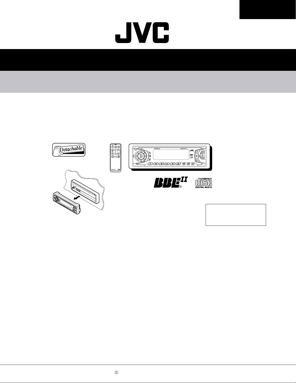
SERVICE MANUAL
CD RECEIVER
KD-SX777
KD-SX777
KD-SX777
Contents
Safety precaution------------------------------------- 1-2
Preventing static electricity
Disassembly method
Adjustment method
-------------------------
-------------------------------
--------------------------------
1-3
1-4
1-9
Area Suffix
................
UR Brazil
Flow of functional operation unit TOC read----
Maintenance of laser pickup----------------------- 1-12
Replacement of laser pickup ---------------------- 1-12
Description of major ICs ---------------------------- 1-13
1-10
COPYRIGHT 2001 VICTOR COMPANY OF JAPAN, LTD.
No.49636
APR. 2001
Page 2

KD-SX777
Safety precaution
CAUTION
!
CAUTION
!
Burrs formed during molding may be left over on some parts of the chassis. Therefore,
pay attention to such burrs in the case of preforming repair of this system.
Please use enough caution not to see the beam directly or touch it in case of an
adjustment or operation check.
1-2
Page 3
KD-SX777
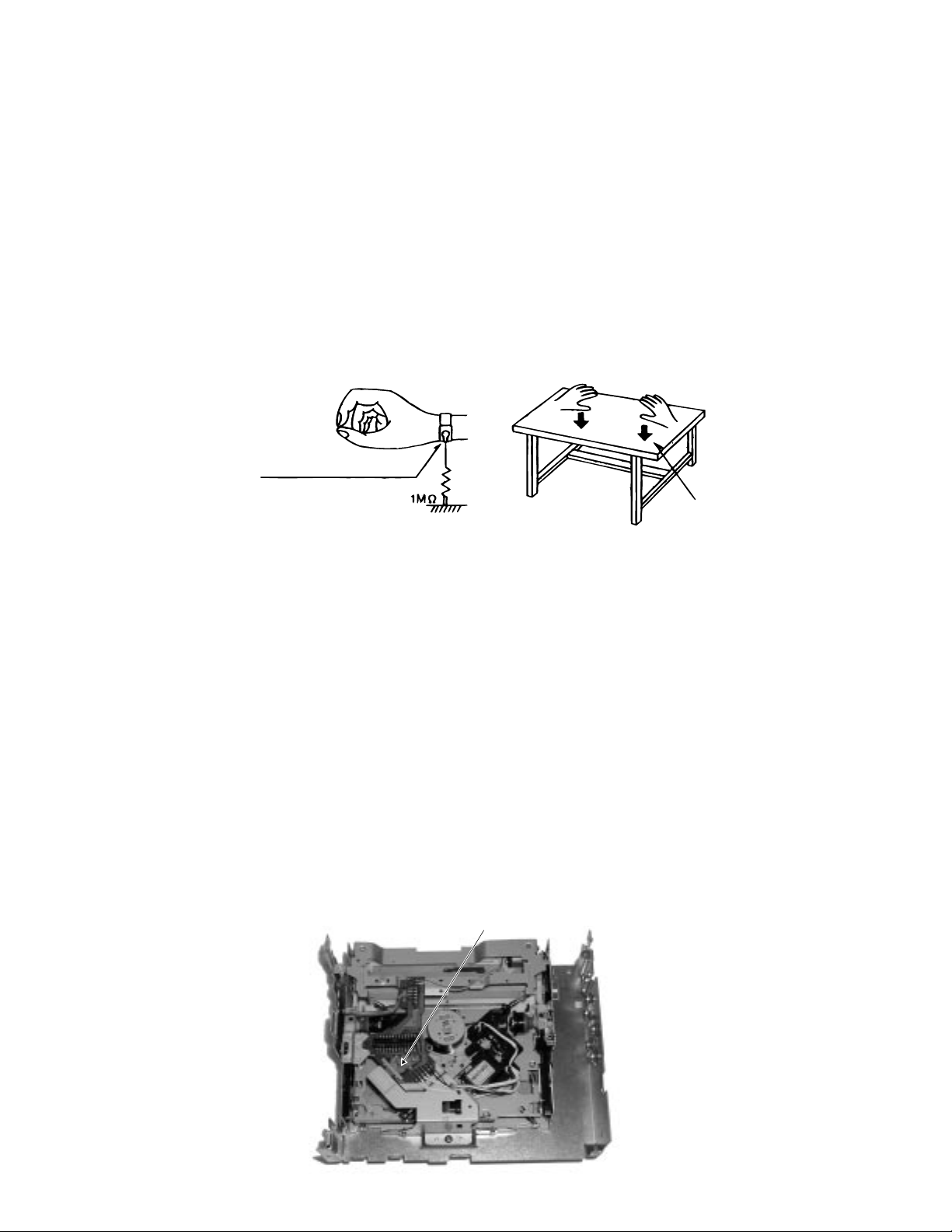
Preventing static electricity
Electrostatic discharge (ESD), which occurs when static electricity stored in the body, fabric, etc. is discharged,
can destroy the laser diode in the traverse unit (optical pickup). Take care to prevent this when performing repairs.
1.1. Grounding to prevent damage by static electricity
Static electricity in the work area can destroy the optical pickup (laser diode) in devices such as DVD players.
Be careful to use proper grounding in the area where repairs are being performed.
1.1.1. Ground the workbench
1. Ground the workbench by laying conductive material (such as a conductive sheet) or an iron plate over
it before placing the traverse unit (optical pickup) on it.
1.1.2. Ground yourself
1. Use an anti-static wrist strap to release any static electricity built up in your body.
(caption)
Anti-static wrist strap
Conductive material
(conductive sheet) or iron plate
1.1.3. Handling the optical pickup
1. In order to maintain quality during transport and before installation, both sides of the laser diode on the
replacement optical pickup are shorted. After replacement, return the shorted parts to their original condition.
(Refer to the text.)
2. Do not use a tester to check the condition of the laser diode in the optical pickup. The tester's internal power
source can easily destroy the laser diode.
1.2. Handling the traverse unit (optical pickup)
1. Do not subject the traverse unit (optical pickup) to strong shocks, as it is a sensitive, complex unit.
2. Cut off the shorted part of the flexible cable using nippers, etc. after replacing the optical pickup. For specific
details, refer to the replacement procedure in the text. Remove the anti-static pin when replacing the traverse
unit. Be careful not to take too long a time when attaching it to the connector.
3. Handle the flexible cable carefully as it may break when subjected to strong force.
4. It is not possible to adjust the semi-fixed resistor that adjusts the laser power. Do not turn it
Shorted part
1-3
Page 4
KD-SX777
Disassembly method
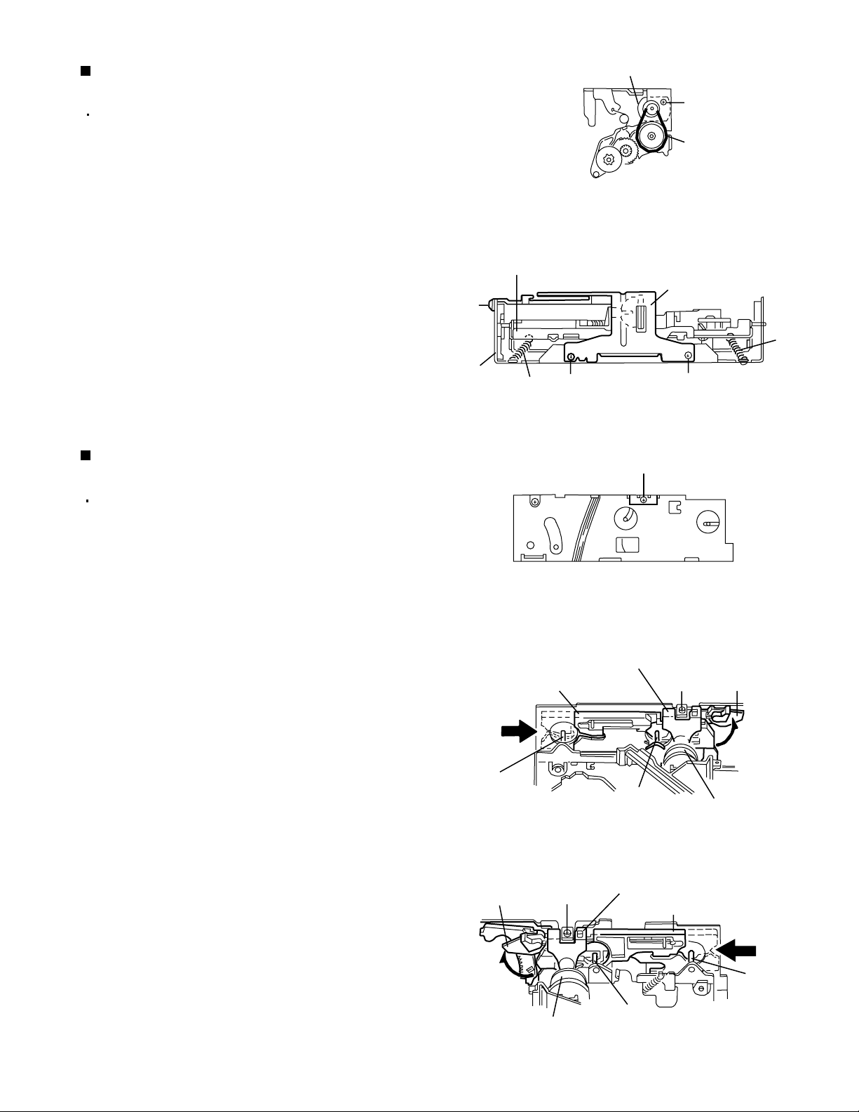
Removing the front chassis (See Fig.1)
1. Remove two screws A and insert a screwdriver to the
joints a on the side of the front chassis and two joints b
on the right side, then detach the front chassis toward the
front side.
Removing the heat sink (See Fig.2 )
1. Remove the three screws B attaching the heat sink on
the left side of the body, and remove the heat sink.
A
a
a
Front chassis
Fig.1
B
A
b
b
B
Removing the bottom cover (See Fig.3 )
1.2.Turn the body upside down.
Insert a screwdriver to the two joints c and two joints d on
both sides of the body and the joint e on the back of the
body, then detach the bottom cover from the body.
B
Heat sink
Fig.2
c
Regulator board
e
Fig. 3
d
1-4
Page 5

KD-SX777
Removing the main amplifier board assembly
(See Fig.4 and 5)
1.
Remove the front chassis.
2.
Remove the bottom cover.
3.
Remove the two screws C attaching the main amplifier
board assembly on the bottom of the body.
4.
Remove the three screws D attaching the main amplifier
board assembly on the back of the body.
Disconnect connector CN501 on the main amplifier board
5.
assembly from the CD mechanism assembly.
Main amplifier board
C
D
CN501
C
Fig.4
D
Fig. 5
Removing the CD mechanism assembly
(See
Fig.6 )
Remove the front chassis.
1.
Remove the bottom cover.
2.
Remove the main amplifier board assembly.
3.
Remove the three screws E attaching the CD mechanism
4.
assembly from the top cover.
Removing the control switch board
(See
Fig.7 and 8 )
1.
Remove the front chassis.
2.
Remove the four screws F attaching the rear cover on the
back of the front panel unit.
Remove the control switch board from the front panel
3.
unit.
CD mechanism assembly
Top cover
E
F
F
Control switch board
Fig. 6
Fig. 7
E
E
F
F
Fig. 8
1-5
Page 6
KD-SX777
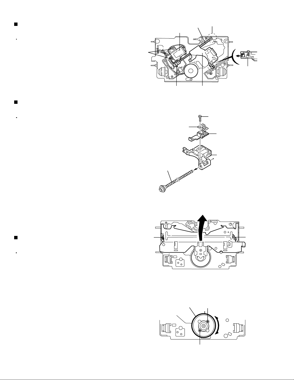
Removing the CD mechanism control
board(See Fig.1 and 2)
Unsolder the part f and g on the CD mechanism
control board.
Remove the stator fixing the CD mechanism control
board and the damper bracket (To remove the stator
smoothly, pick up the center part).
Remove the screw F attaching the CD mechanism
control board.
Remove the CD mechanism control board in the
direction of the arrow while releasing it from the two
damper bracket slots i and the front bracket slot j.
Disconnect the flexible wire from connector on the
pickup unit.
ATTENTION:
Turn the FD gear in the direction of the
arrow to move the entire pickup unit to
the appropriate position where the
flexible wire of the CD mechanism unit
can be disconnected easily (Refer to
Fig.2).
CD mechanism ass’y
m
Front bracket
Damper bracket
I
g
F
Fig.1
Pickup unit
I
j
Flexible wire
f
m
h
I
i
CD mechanism
control board
Shift the lock
FD gear
k
G
Loading motor
Pull outward
Fig.2
CD mechanism control board
Front bracket
Fig.3
Front bracket
k
G
Pull outward
1-6
Flame
Fig.4
Page 7
KD-SX777
Removing the loading motor
(See Fig.3 to 5)
Prior to performing the following procedure, remove
the CD mechanism control board.
1.
Remove the two springs k attaching the CD mechanism
ass’y and the front bracket.
2.
Remove the two screws G and the front bracket
while pulling the flame outward.
3.
Remove the belt and the screw H from the loading
motor.
Removing the CD mechanism ass’y
(See Fig.1, 6 to 9)
CD mechanism ass’y
I
Flame
Loading motor
m
H
Belt
Fig.5
Damper bracket
m
I
Fig.6
I
I
Prior to performing the following procedure, remove
the CD mechanism control PWB and the front
bracket (loading motor).
1.
Remove the three screws I and the damper bracket.
2.
Raise the both sides fix arms and move the fix plates
in the direction of the arrow to place the four shafts l
as shown in Fig.8 and 9.
3.
Remove the CD mechanism ass’y and the two
springs m attaching the flame.
4.
Remove the two screws J and both sides rear
damper brackets from the dampers. Detach the CD
mechanism ass’y from the left side to the right side.
ATTENTION:
The CD mechanism ass’y can be
removed if only the rear damper
bracket on the left side is removed.
Fix plate (L)
l
Fix arm (R)
Fig.7
Rear damper bracket
l
Fig.8
Rear damper bracket
J
Fix plate(R)
J
Fix arm (L)
Damper
Damper
l
l
Fig.9
1-7
Page 8
KD-SX777
Removing the feed motor ass’y
(See Fig.10)
Prior to performing the following procedure, remove
the CD mechanism control board, the front bracket
(loading motor) and the CD mechanism ass’y.
1.
Remove the two screws K and the feed motor ass’y.
Removing the pickup unit
(See Fig.10 and 11)
*Prior to performing the following procedure, remove
the CD mechanism control board, the front bracket
(loading motor), the CD mechanism ass’y and the
feed motor ass’y.
1.
Detach the FD gear part of the pickup unit upward.
Then remove the pickup unit while pulling out the
part n of the FD screw.
Feed motor ass’y
K
FD gear
Nut push spring plate
FD screw
Pickup unit
Fig.10
Part n
Part O
Pickup unit
L
Pickup mount nut
Pickup unit
ATTENTION:
2.
Remove the screw L attaching the nut push spring
plate and the pickup mount nut from the pickup unit.
Pull out the FD screw.
When reattaching the pickuap unit,
reattach the part o of the pickup unit,
then the part n of the FD screw.
Removing the spindle motor
(See Fig.12 and 13)
Prior to performing the following procedure, remove
the CD mechanism control board, the front bracket
(loading motor), the CD mechanism ass’y and the
feed motor ass’y.
1.
Turn up the CD mechanism ass’y and remove the
two springs p on both sides of the clamper arms.
Open the clamper arm upward.
2.
Turn the turn table, and remove the two screws M
and the spindle motor.
FD screw
p
Spindle motor
Fig.11
p
Fig.12
M
1-8
M
Fig.13
Page 9
Adjustment method
KD-SX777
Test instruments required adjustment
1.Digital oscilloscope (100MHz)
2.AM Standard signal generator
3.FM Standard signal generator
4.Stereo modulator
5.Electric voltmeter
6.Digital tester
7.Tracking offset meter
8.Test Disc JVC : CTS-1000
9.Extension cable for check
EXTGS004-26P
Standard measuring conditions
Power supply voltage DC14.4V(10.5
Load impedance 4 (4 to 8 allowance)
Line-out Level/Impedance
KD-SX770 : 2.0 V/20k load(full scale)
Output impedance : 1k
Standard volume position
Balance and Bass & Treble volume : Indication "0"
BBE : OFF
Frequency Band
FM
AM
Dummy load
Exclusive dummy load should be used for AM,and FM.
For FM dummy load, there is a loss of 6dB between SSG output
and antenna input. The loss of 6dB need not be considered
since direct reading of figures are applied in this working
standard.
–
16V)
1 – 3 87.5MHz – 107.9MHz
530kHz – 1710kHz
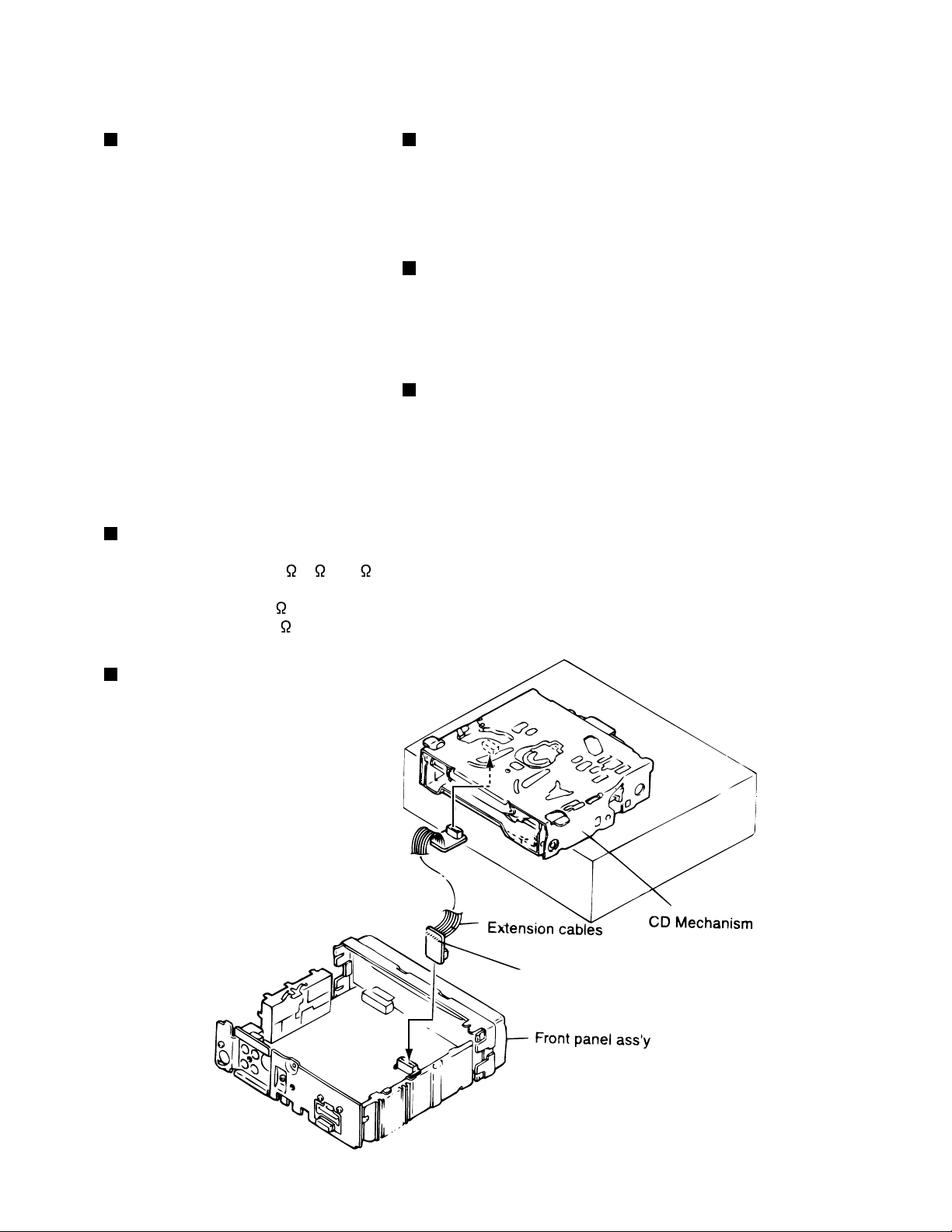
How to connect the extension cable for adjusting
CN701
CN501
EXTGS004-26P
1-9
Page 10
KD-SX777
Flow of functional operation unit TOC read
Power ON
When the pickup correctly moves
to the inner area of the disc
Set Function CD
When the laser diode correctly
emits
Microprocessor
commands
FMO
TC9462"53"
FEED MOTOR
+TERMINAL
IC581"6"
REST SW
When correctly focused
FEO
TA2109
14
Focus Servo Loop ON
$83
$82
$81
5V
Hi-Z
0V
6V
4V
2V
OFF
ON
Pickup feed to the inner area
2.2V
RF signal eye-pattern
remains closed
RF signal eye-pattern
opens
Disc inserted
YES
Laser emitted
Focus search
Disc rotates
Tracking loop closed
TOC readout
YES
Microprocessor
commands
SEL
TC9462
LD
CN501
57
1
"No disc"
display
When the disc correctly rotates
Microprocessor
commands
DMO
TC9462
Spindle
motor(-)
IC581"5"
$84 $86 $ A200
55
Acceleration Servo CLV
Rough
Servo
0.5 Sec 0.5 Sec
$84
5V
0V
4V
0V
5V
2.2V
0V
6V
3.2
2V
1-10
Jump to the first track
Play
Tracking Servo Loop ON
RF signal
Rough Servo Mode
CLV Servo Mode
(Program Area)
CLV Servo Mode
(Lead-In Area;
Digital: 0)
Page 11

Feed section
Is the voltage output at
IC541 pin "53" 5V or 0V?
YES
Is 4V present at both
sides of the feed motor?
YES
NO YES NO
NO
Is the wiring for IC521
(90)~(100) correct?
NO
Is 6V or 2V present at
IC581 "6" and "7"?
NO
Is 5V present at IC581
pin "20"?
Check the vicinity of
IC521.
YES
Check the feed motor
connection wiring.
YES
Check CD 9V
KD-SX777
and 5V.
Check the feed motor.
Focus section
When the lens is
moving:
Does the S-search
waveform appear at
IC581 pins "8" and "9"?
Spindle section
Is the disk rotated?
YES
Does the RF signal
appear at RF(TP1)?
YES
Is the RF waveform at
RF(TP1)distor
Proceed to the Tracking
section
ted?
YES
4V
Check IC581.
NO
YES
NO
NO
NO
Check the circuits in
the vicinity of IC581
pins "8","9"and"15".
Check the pickup and
its connections.
Is 4V present at IC581
pins "4" and "5"?
Check the spindle motor
and its wiring
Check the circuits in the
vicinity of IC501 "19"~
"24" or the pickup
YES
YES
NO
Is 4V present at IC521
pins "55" ?
Check the vicinity of
IC581.
NO
YES
Check IC501 and
IC521.
Tracking section
When the disc is rotated
at first:
Is the tracking error signal
output at IC501 "12"?
Check IC521.
Approx. 1.2V
YES
YES YES
Check the circuit in the
vicinity of IC501 pins
"2"~"12".
Check the pickup and
its connections.
1-11
Page 12

KD-SX777
Maintenance of laser pickup
(1) Cleaning the pick up lens
Before you replace the pick up,please try to
clean the lens with a alcohol soaked cotton
swab.
(2) Life of the laser diode
When the life of the laser diode has expired,
the following symptoms will appear.
(1) The level of RF output (EFM output:ampli
tude of eye pattern) will be low.
Is RF output
1.3 0.4Vp-p?
YES
O.K
(3) Semi-fixed resistor on the APC PC board
The semi-fixed resistor on the APC printed
circuit board which is attached to the pickup
is used to adjust the laser power. Since this
adjustment should be performed to match the
characteristics of the whole optical block,
do not touch the semi-fixed resistor.
If the laser power is lower than the specified
value, the laser diode is almost worn out, and
the laser pickup should be replaced.
If the semi-fixed resistor is adjusted while
the pickup is functioning normally, the laser
pickup may be damaged due to excessive current.
NO
Replace it.
Replacement of laser pickup
Turn off the power switch and,disconnect the
power cord.
Replace the pickup with a normal one.(Refer
to "Pickup Removal" on the previous page)
Plug the power cord in, and turn the power on.
At this time, check that the laser emits for
about 3seconds and the objective lens moves
up and down.
Note: Do not observe the laser beam directly.
1-12
Play a disc.
Check the eye-pattern at RF(TP1).
Finish.
Page 13

+
+
-
-
+
+
-
-
-
+
+
Description of major ICs
BA3220FV-X(IC341/IC441) : Line Out Amp
KD-SX777
CL-
14
LGND
13
14
3220
17
OUTL OUTR RGND
1112
8
CR-
10
9
CR+
8
REFR
1
2
Vcc
3
INL
4
NFLCL+
REFR
FILTER
56
FIL
NFR
7
INR
1-13
Page 14

KD-SX777
UPD178078GF-543 (IC701): SYSTEM CPU
1.Terminal layout
2.Block diagram
TO0/VTR-CONT
TI00/POWER
TI01/CD-ON
TI50/MUTE
TO50/NC
TI51/STAGE
TO51/NC
SI0/SB0/SDA0/NC
SO0/SB1/SDA1/VOL-DA
SCK0/SCL/VOL-CLK
SI1/JBUS-SI
SO1/JBUS-SO
SCK1/JBUS-SCK
STB/NC
BUSY/NC
SI3/NC
SO3/LCD-DA
SCK3/SCL/LCD-CLK
TXD0/LM1
RXD0/LM0
INTP0/NC
INTP7/NC
BEEP0/BUZZER
BUZ/NC
RESET
X1
X2
V
DD
PORT
GNDPORT
V
DD
VM45/VTR-LOGIC
REGOSC
REGCPU
GND0
GND1
16-bit TIMER/
EVENT COUNTER
8-bit TIMER/
EVENT COUNTER 0
8-bit TIMER/
EVENT COUNTER 1
WATCHDOG TIMER
BASIC TIMER
SERIAL
INTERFACE 0
SERIAL
INTERFACE 1
SERIAL
INTERFACE 3
UART0
8
INTERRUPT
CONTROL
BUZER OUTPUT
SYSTEM
CONTROL
VOLT AGE
REGULATOR
1
~
30
100 ~ 81
31 ~ 50
80
~
51
78k/0
CPU
CPRE
ROM
PD178078
:3Kbyte
PD178076
:2Kbyte
RESET
CPU
PERIPHERAL
OSC
V
V
CPU
ROM
PD178078
:60Kbyte
PD178076
:48Kbyte
PORT 0
PORT 1
PORT 2
PORT 3
PORT 4
PORT 5
PORT 6
PORT 7
PORT10
PORT 12
PORT 13
A/D
CONVERTER
FREQUENCY
COUNTER
PLL
PLL
VOLT AGE
REGULATOR
NC,JBUS-INT,SW1,
8
REMOCON,PS1,PS2,
DETACH,NC
KEY0,KEY1,KEY2,LEVEL,
8
SM,Add:"OPEN",NC,
JBUS-SI,JBUS-SO,
8
JBUS-SCK,NC,VOL-DA,
VOL-CLK
VTR-LOGIC,VTR-CONT,
8
POWER,CD-ON,MUTE,
BUZZER,NC
8
NC,Add:"Dimmer"
NC,LCD-CE,SW2,SW3,
8
SW4,RST-SW,ENC1,ENC2
MONO,SEEK/STOP,
FM/AM,Add:DIMIN,
8
ANTENNA,TEL,
STAGE1,STAGE2
NC,LCD-DA,LCD-CLK,
8
JBUS-/O,LM0,LM1,BUCK,
CCE
3
SD/ST,NC,IFC
5
BUS0,BUS1,BUS2,BUS3,
RST
8
NC
AN10/KEY0
8
AN17/NC
DD
AV
AV
SS
AMIFC/NC
FMIFC/IFC
EO0
EO1
VCOL
VCOH
DD
PLL
V
GNDPLL
TELMUTING
1-14
IC
GND2
Page 15

KD-SX777
3.Pin function
Pin
NO.
1
2
3
4
5
6
7
8
9
10
11
12
13
14
15
16
17
18
19
20
21
22
23
24
25
26
27
28
29
30
31
32
33
34
35
36
37
38
39
40
41
42
43
44
45
46
47
48
49
50
NC
JBUS-INT
JBUS-SI
JBUS-SO
JBUS-SCK
NC
NC
NC
VOL-DA
VOL-CLK
NC
LCD-DA
LCD-CLK
JBUS-I/O
NC
LCD-CE
SW2
SW3
SW4
RST-SW
ENC1
ENC2
KEY0
KEY1
KEY2
LEVEL
AVDD
SM
OPEN
NC
NC
AVSS
REGCPU
VDD
REGOSC
X2
X1
GND0
SD/ST
GND2
NC
IFC
VDDPLL
OSC-INPUT
NC
GNDPLL
AME0
FME0
ICVPP
RESET
UPD178078GF(1/2)
I/OSymbol
-
Non connection
I
JVC BUS COMMUNICATION LINE
I
JVC BUS COMMUNICATION LINE
O
JVC BUS COMMUNICATION LINE
O
JVC BUS COMMUNICATION LINE
-
Non connection
-
Non connection
-
Non connection
O
VOL IC COMMUNICATION LINE
O
VOL IC COMMUNICATION LINE
-
Non connection
O
CD DRIVER COMMUNICATION LINE
O
LCD DRIVER COMMUNICATION LINE
O
JVC BUS OUTPUT SELECT
-
Non connection
O
LCD DRIVER COMMUNICATION LINE
I
CD MECHA SW
I
CD MECHA SW
I
CD MECHA SW
I
TRAVERSE MECHA REST SW
I
ENCODER INPUT
I
ENCORDER INPUT
I
KEY INPUT
I
KEY INPUT
I
KEY INPUT
I
AUDIO LEVEL INPUT
-
-
I
SIGNAL LEVEL METER INPUT
I
DOOR OPEN DATECTION
-
Non connection
-
-
-
-
-
-
-
-
-
SYSTEM CLOCK
I
SYSTEM CLOCK
-
-
I
Connected to GND
-
STATION DETECTOR & STEREO IND.
-
-
I
Non connection
-
IF COUNT INPUT
I
-
-
FM,AM OSC INPUT
-
Non connection
O
-
O
PLL ERROR OUTPUT FOR AM
-
PLL ERROR OUTPUT FOR FM
I
SETTING TO WRITE FOR FLASH
FUNCTION
SYSTEM RESET
1-15
Page 16

KD-SX777
Pin
NO.
51
52
53
54
55
56
57
58
59
60
61
62
63
64
65
66
67
68
69
70
71
72
73
74
75
76
77
78
79
80
81
82
83
84
85
86
87
88
89
90
91
92
93
94
95
96
97
98
99
100
SW1
REMOCON
VTR-LOGIC
VTR-CONT
POWER
CD-ON
MUTE
NC
BUZZER
NC
NC
NC
NC
NC
NC
NC
NC
NC
LM0
LM1
BUCK
CCE
BUS0
BUS1
BUS2
BUS3
RST
PS1
PS2
DETACH
NC
GND1
MONO
SEEK/STOP
FM/AM
DIMIN
ANT
TEL MUTE
STAGE1
STAGE2
NC
NC
NC
NC
NC
NC
NC
DIMMER
VDDPORT
GNDPORT
I/OSymbol
I
I
-
O
O
O
-
I
-
-
-
-
-
-
-
-
O
O
O
O
I/O
I/O
I/O
I/O
O
I
I
I
-
O
O
O
I
O
I
I
I
-
-
-
-
-
-
O
-
-
UPD178078GF(2/2)
FUNCTION
CD MECHA SW
REMOCON INPUT
Non connection
Non connection
POWER CONT.
CD POWER CONT.
MUTE CONT
Non connection
BEEP FOR SW OPERATION
Non connection
Non connection
Non connection
Non connection
Non connection
Non connection
Non connection
Non connection
Non connection
CD MECHA DRIVER CONT.
CD MECHA DRIVER CONT.
CD LSI COMMUNICATION LINE
CD LSI COMMUNICATION LINE
CD LSI COMMUNICATION LINE
CD LSI COMMUNICATION LINE
CD LSI COMMUNICATION LINE
CD LSI COMMUNICATION LINE
CD LSI COMMUNICATION LINE
ACC DETECTION INPUT
MEMORY DETECTION
DETACH DETECTION
Non connection
MONO BY FORCE
SWITCHING SEEK & STOP
BAND SW
OUTPUT L
ILM CONTROL
ANT COTROL
TEL MUTE IN
MODEL SETTING
MODEL SETTING
Non connection
Non connection
Non connection
Non connection
Non connection
Non connection
Non connection
DIMMER CONTROL
-
-
1-16
Page 17

TA2109F-X (IC501) : RF amp.
1. Pin layout
24 13
112
2. Block diagram
SBAD
13
FEO
14
10pF
FEN
15
10k ohm
VRO
16
21k ohm
20k ohm
RFRP
17
RFIS
18
20k ohm
RFGO
19
50k ohm
36pF
7.96k ohm
50uA
20k ohm
15k ohm 30k ohm
15k ohm
20uA
10k ohm
21k ohm
12k ohm
12k ohm
PEAK
BOTTOM
10k ohm
10k ohm
30k ohm
21k ohm 29k ohm
24k ohm 24k ohm
180k ohm
1.74k ohm
20pF
65uA
10k ohm
47k ohm
SW3
13k ohm
7.67k ohm
3 STATE
DET.
SW1
1k ohm
SW2
680 ohm
2.12k ohm
20pF
LDC
TEO
TEN
2VRO
TEB
SEL
LDO
MDI
KD-SX777
12
11
10
9
8
7
6
3. Pin function
Pin
SymbolI/O
No.
Vcc
FNI
FPI
TPI
TNI
MDI
SEL
TEB
I
I
I
I
I
O
I
I
O
I
O
10
11
12
1
2
3
4
5
6
7
8
9
LDO
2VRO
TEN
TEO
RFGC
20
AGCI
21
re=130 ohm
RFO
22
GND
23
RFN
24
23.5k ohm
3.3k ohm
12k ohm
1.53k ohm
3.3k ohm
Pin function
Power supply input terminal
Main beam I-V amp input terminal
Main beam I-V amp input terminal
Sub beam I-v input terminal
Sub beam I-V input terminal
Monitor photo diode amp input terminal
Laser diode amp output terminal
Laser diode control signal input terminal
T. error balance adj. signal input terminal
Reference voltage output terminal
TE amp negative input terminal
TE error signal output terminal
180k ohm
40pF
180k ohm
Pin
No.
13
14
15
16
17
18
19
20
21
22
23
24
180k ohm
20pF
60k ohm
60k ohm
40pF
SymbolI/O
SBAD
RFRP
RFGO
RFGC
FEO
FEN
VRO
RFIS
AGCI
RFO
GND
RFN
O
O
I
O
O
I
O
I
I
O
-
I
TNI
TPI
FPI
FNI
Vcc
5
4
3
2
1
I-I
I-I
20k ohm
20k ohm
20k ohm
20k ohm
Pin function
Sub beam adder signal output terminal
Focus error signal output terminal
FE amp negative input terminal
Reference voltage (VREF) output terminal
Track count signal output terminal
RFRP detect circuit input terminal
RF gain signal output terminal
RF amplitude adj. control signal input terminal
RF signal amplitude adj. amp input terminal
RF signal output terminal
Ground terminal
RF amp negative input terminal
1-17
Page 18

KD-SX777
BD3860K (IC301):
Audio sound processor
1.Terminal layout
33
34
44
1
23
22
12
11
2.Pin function
Pin No.
Symbol
I/O Function
1 A2 I CH2 input pin A
2 B2 I CH2 input pin B
3 C2 I CH2 input pin C
4 D2 I CH2 input pin D
5 FIL - 1/2 VCC pin
6 GND - Ground pin
7 SI I Serial data receiving pin
8 SC I Serial clock receiving pin.
9 VCC - Power supply pin
10 OUTR2 O CH2 rear output pin
11 OUTF2 O CH2 front output pin
12 OUTR1 O CH1 rear output pin
13 OUTF1 O CH1 front output pin
14 BOUT1 O CH1 bass filter setting pin
15 BNF1 I CH1 bass filter setting pin
16 BOUT2 O CH2 bass filter setting pin
17 BNF2 I CH2 bass filter setting pin
18 TNF2 I CH2 treble filter setting pin
19 TNF1 I CH1 treble filter setting pin
20 TIN2 I CH2 treble input pin
21 BBOUT2 O CH2 BBE II signal output pin
22 MIX2 I CH2 output mix amplifier inverse input pin
23 VCA2 O CH2 high pass VCA output pin
24 LF2 I CH2 low pass filter setting pin
25 HF2 I CH2 high pass filter setting pin
26 DET2 I CH2 high pass attack/release time setting pin
27 DEF I BBE II on/off switching time constant pin
28 DET1 I CH1 high pass attack/release time setting pin
29 TIN1 I CH1 treble input pin
30 BBOUT1 O CH1 BBE II signal output pin
31 MIX1 I CH1 output mix amplifier inverse input pin
32 VCA1 O CH1 high pass VCA output pin
33 LF1 I CH1 low pass filter setting pin
34 HF1 I CH1 high pass filter setting pin
35 LOUD1 I CH1 loudness filter setting pin
36 VIN1 I CH1 main volume input pin
37 LOUD2 I CH2 loudness filter setting pin
38 VIN2 I CH2 main volume input pin
39 SEL2 O CH2 Input gain output pin
40 SEL1 O CH1 Input gain output pin
41 A1 I CH1 input pin A
42 B1 I CH1 input pin B
43 C1 I CH1 input pin C
44 D1 I CH1 input pin D
1-18
Page 19

3.Block diagram
A1
B1
C1
D1
B2
C2
D2
A2
GND FIL VCC
956
SEL1
VIN1 LOUD1
HF1 LF1 DET1 VCA1 MIX1 BBOUT1
3132283334353640
30
TIN1 TNF1
29
19
BNF1 BOUT1
1415
POWER
SUPPLY
INPUT
41
42
43
44
1
2
3
4
INPUT
SELECTOR
GAIN
Oto 18dB
INPUT
GAIN
Oto 18dB
39
SEL2
MAIN
VOLUME
Oto -48dB
LOUDNESS
MAIN
VOLUME
Oto -48dB
LOUDNESS
3738
VIN2 LOUD2
LO CONTOUR(f=100Hz) 5dB
PROCESS CONTROL +3to12dB
(f=10KHz)
LOGIC
LO CONTOUR(f=100Hz) 5dB
PROCESS CONTROL +3to12dB
(f=10KHz)
25
24
HF2 LF2 DET2 VCA2 MIX2 BBOUT2
23
26
BASS
-14to+14dB
BASS
-14to+14dB
18
202122
TIN2 TNF2
TREBLE
-14to+14dB
TREBLE
-14to+14dB
17
BNF2 BOUT2
16
FADER
CH1 FRONT
Oto -54dB
FADER
CH1 REAR
Oto -54dB
FADER
CH2 FRONT
Oto -54dB
FADER
CH1 REAR
Oto -54dB
13
12
7
8
27
10
11
OUTR1
S1
SC
DEF
OUTR2
OUOTF2
1-19
KD-SX777
Page 20

KD-SX777
LA4743K(IC351):Power AMP
1.Block diagram
IN 1
TAB
IN 2
+
0.22 F
+
0.22 F
11
1
12
Vcc 1/2 Vcc 3/4
6 20
-
+
Protective
circuit
-
+
2200 F 0.022 F
+
9
-
7
+
OUT 1+
OUT 1-
PWR GND1
8
+
OUT 2+
5
-
OUT 2-
3
PWR GND2
2
ST BY
R.F
47 F
IN 3
PRE GND
IN 4
+5V
ST ON
+
0.22 F
N.C
+
0.22 F
4
Stand by
Switch
Mute
10
+
Ripple
Filter
Mute
22
circuit
3.3 F
+
15
-
+
-
17
19
10K
+
OUT 3+
OUT 3-
Low Level
Mute ON
25
18
21
23
PWR GND3
OUT 4+
OUT 4-
13
14
Protective
circuit
-
+
+
-
1-20
ON TIME C
22 F
Muting &
16
+
ON Time Control
Circuit
PWR GND4
24
Page 21

2.Terminal layout
3.Pin function
SymbolPin No. Function
KD-SX777
LA4743K
1
2
3
4
5
6
7
8
9
10
11
12
13
14
15
16
17
18
19
20
21
22
23
24
25
TAB
GND
OUTRFSTBY
OUTRF+
VCC1/2
OUTRRGND
OUTRR+
RIPPLE
INRR
INRF
SGND
INLF
INLR
ONTIME
OUTLR+
GND
OUTLRVCC3/4
OUTLF+
MUTE
OUTLFGND
NC
Header of IC
Power GND
Outpur(-) for front Rch
Stand by input
Output (+) for front Rch
Power input
Output (-) for rear Rch
Power GND
Output (+) for rear Rch
Ripple filter
Rear Rch input
Front Rch input
Signal GND
Front Lch input
Rear Lch input
Power on time control
Output (+) for rear Lch
Power GND
Output (-) for rear Lch
Power input
Output (+) for front Lch Add
Muting control input
Output (-) for front Lch Add
Power GND
Non connection
1-21
Page 22

KD-SX777
TC9462F(IC521) : DSP&DAC
1.Pin layout & Block Diagram
RST
DD
XV
80
79
81DV
SR
82RO
83DV
DD
84DVR
85LO
86DV
SL
87TEST1
88TEST2
89TEST3
90BUS0
91BUS1
92BUS2
93BUS3
94V
DD
95V
SS
96BUCK
97CCE
98TEST4
99TSMOD
100
1 2 3
TEST0
XO78XI
LPF
HSO
Micon
interface
UHSO
SS
XV
77
4 5
EMPH
DD
V
75
76
1bit
DAC
PXO
SS
PXI
V
74
73
Clock
generator
Correction
circuit
Audio out
circuit
6
7 8 9 10 11 12 13
SS
V
BCK
LRCK
AOUT
TESIO1
72
DOUT
71
TESIN
MBOV
DACT
69
70
Address circuit
16KRAM
Digital out
IPF
CKSE
SBOK
DMOUT
68
CLCK
IO3
IO265IO164IO063V
67
66
ROM
Automatic adjustment
RAM
Synchronous
guarantee
EFM decode
Sub code
decoder
14 15
16 17 18 19 20 21 22
SS
DD
V
V
DATA
SFSY
SS
DD
V
61
62
Servo
control
Digital equalizer
circuit
CLV servo
SBSY
SPCK
FLGD60FLGC59FLGB58FLGA57SEL562V
PWM D/A
A/D
Status
TMAX
23 24 25
DD
COFS
MONIT
V
SPDA
REF
DMO54FVO53FMO52TEBC51RFGC
55
+
-
Data
slicer
VCO
+
PLL
26
27 28
PDO
ZDET
HSSW
50 V
REF
49 TRO
48 FOO
TEZI
47
+
-
-
-
29
+
TMAXS
30
TMAX
46 TEI
45 TSIN
44 SBAD
43 FEI
42 RFRP
41 RFZI
40 RFCT
39 AV
DD
38 RFI
37 SLCO
36 AV
SS
35 VCOF
34 VCOREF
33 PV
REF
32 LPFO
31 LPFN
2.Pin function
Pin No.
10
11
1213SBOK
1
2
3
4
5
6
7
8
9
Symbol
TEST0
HSO
UHSO
EMPH
LRCKOO
V
SS
BCK
AOUT
DOUT
MBOV
IPF
CLCK
Function
I/O
Test mode terminal.Normally, Keep at open.
I
Playback speed mode flag output terminal.
UHSO
HSO
O
H
H
L
O
L
PLAYBACK SPEED
H
L
H
L
Nomal
2 times
4 times
--
Subcode Q data emphasis flag output terminal.Emphasis ON at "H" level
and OFF at "L"level.The output polarity can invert by command.
Channel clock output terminal.(44.1khz)L-ch at "L" level and R-ch at
"H" level. the output polarity can invert by command.
Digital GND terminal.
--
O
Bit clock output terminal.(1.4112MHz)
Audio data output terminal.
O
Digital data output terminal.
O
Buffer memory over signal output terminal. Over at "H" level.
O
Correction flag output terminal. At "H" level,AOUT output is made to
O
correction impossibility by C2 correction processing.
Subcode Q data CRCC check adjusting result output terminal.
O
The adjusting result is OK at "H" level.
Subcode P~W data readout clock input/output terminal.
I/O
This terminal can select by command bit.
TC9462F(1/2)
Remarks
With pull-up resistor.
--
--
--
--
--
--
--
--
--
--
--
1-22
Page 23

Pin No.
14
15
16
17
18
19
20
21
22
2324V
25
26
27
28
29
Symbol
V
DD
V
SS
DATA
SFSY
SBSY
SPCK
SADA
COFS
MONIT
DD
TESIO0--I
P2V
REF
HSSW
ZDET
PDO
TMAXS
I/O
--
Digital power supply voltage terminal.
--
Digital GND terminal.
O
Subcode P~W data output terminal.
O
Play-back frame sync signal output terminal.
O
Subcode block sync signal output terminal.
O
Processor status signal readout clock output terminal.
O
Processor status signal output terminal.
O
Correction frame clock output terminal. (7.35kHz)
Internal signal (DSP internal flag and PLL clock) output terminal.Selected
O
by command.This terminal output the text data with serial by command.
Digital power supply voltage terminal.
Test input/output terminal.Normally,keep at "L" level.
The terminal that inputted the clock for read of text
data by command.
--
PLL double reference voltage supply terminal.
O
2/8 times speed at "VREF" voltage.
1bit DA converter zero detect flag output terminall.
O
Phase differnce signal output terminal of EFM signal
O
and PLCK signal.
O
TMAX detection result output terminal. Selected by
command bit (TMPS).
KD-SX777
TC9462F(2/3)
Remarks
--
--
--
--
--
--
--
--
--
--
--
2-state output.(PVREF,Hiz)
3-state output.
(P2VREF,PVREF,VSS)
3-state output.
(P2VREF,PVREF,VSS)
30
31
32
33
34
35
36
37
38
39
40
41
42
43
TMAX
LPFN
LPFO
PVREF
VCORE
VCOF
AVSS
SLCO
RFI
AVDD
RFCT
RFZI
RFRP
FEI
TMAX detection result output terminal. Selected by
O
command bit (TMPS).
DIFFERENCE RESULT
Longer than fixed freq.
Shorter than fixed freq.
Within the fixed freq.
I
LPF amplifier inverting input terminal for PLL.
O
LPF amplifier output terminal for PLL.
--
PLL reference voltege supply teminal.
VCO center frequency reference level terminal.
I
TMAX OUTPUT
"P2VREF"
"VSS"
"Hiz"
Normally, keep at "PVREF" level.
O
VCO filter terminal.
--
Analog GND terminal.
O
Data slice level output terminal.
I
RF signal input terminal.
Analog power suppyl coltage terminal.
-RFRP signal center level input terminal.
I
RFRP zero cross input teminal.
I
RF ripple signal input terminal.
I
Forcus error signal input terminal.
I
3-state output.
(P2VREF,Hiz,VSS)
Analog input.
Analog output.
--
--
Analog output.
--
Analog output.
Analog input. (Zin:
selected by command)
Analog output.
Analog output. (Zin:50k)
Analog input.
Analog input.
Analog input.
1-23
Page 24

KD-SX777
Pin No.
44
45
46
47
48
49
50
51
52
53
54
55
56
57
58 61
62
63
64 67
68
69
70
71
72
73
74
75
76
77
78
79
80
81
82
83
84
85
86
87 89
90 93
94
95
96
97
98
99
100
Symbol
SBAD
TSIN
TEI
TEZI
FOO
TRO
VREF
RFGC
TEBC
FMO
FVO
DMO
2VREF
SEL
FLGA D
VDD
VSS
IO0 3
DMOUT
CKSE
DACT
TESIN
TESIO1
VSS
PXI
PXO
VDD
XVSS
XI
XO
XVDD
DVSR
RO
DVDD
DVR
LO
DVSL
TEST1 3
BUS0 3
VDD
VSS
BUCK
CCE
TEST4
TSMOD
RST
I/O
Sub-beam adder signal input terminal
I
Test input terminal Normally, keep at "vref" level
I
Tracking error signal input terminal. Take in at tracking servo ON.
I
Tracking error zero cross input terminal
I
Focus servo equalizer output terminal
O
Tracking servo equalizer output terminal
O
Analog reference voltage supply terminal
RF amplitude adjustment control signal output terminal
O
Tracking balance control signal output terminal
O
Feed equalizer output terminal
O
Speed error signal or feed search equalizer output terminal
O
Disk equalizer output terminal
O
Synchronize to PXO)
Analog double reference voltage supply terminal
APC circuit ON/OFF indication signal output terminal
O
External flag output terminal for internal signal
O
Digital power supply voltage terminal
Digital GND terminal
General I/O terminal
I/O
This terminal control IO0 IO3 terminal
I
Normally, keep at open
I
DAC test mode terminal. Normally, keep at open
I
Test input terminal, Normally, keep at "L" level
I
Test input/output terminal. Normally, keep at "L" level
I
Digital GND terminal
Crystal oscillator connecting input terminal for DSP
I
Crystal oscillator connecting output terminal for DSP
O
Digital power supply voltage terminal
Oscillator GND terminal for system clock
Crystal oscillator connecting input terminal for system clock
I
Crystal oscillator connecting output terminal for system clock
O
Oscillator power supply voltage terminal for system clock
Analog GND terminal for DA converter (Rch)
R channel data forward output terminal
O
Analog supply voltage terminal for DA converter
Reference voltage terminal for DA converter
L channel data forward output terminal
O
Analog GND terminal for DA converter (Lch)
Test mode terminal . Normal keep at open
I
Micon interface data input/output terminal
I/O
Digital power supply voltage terminal
Digital GND terminal
Micon interface clock input terminal
I
Command and data sending/receiving chip enable signal
I
FunctionFunction
(PWM carrier=88.2kHz for DSP,
input terminal
Test mode terminal. Normal, keep at open
I
Local test mode selection terminal
I
Reset signal input terminal. Reset at "L" level
I
TC9462F(3/3)
Remarks
Analog input.
Analog input.
Analog input.
Analog input
.
(Zin:10k)
Analog output
REF AVss)
(2V
3-state PWM signal
output.
2V
REF.VREF.VSS
(PWM carrier=88.2kHz)
3-state output
(2V
REF.VREF.VSS)
--
--
--
--
--
-With pull-up resistor.
With pull-up resistor.
With pull-up resistor.
Analog input.
Analog input.
--
--
--
--
--
--
--
--
--
--
--
--
--
-With pull-up resistor.
Schmit input.
With pull-up resistor.
--
-Schmit input.
Schmit input.
With pull-up resistor.
With pull-up resistor.
With pull-up resistor.
1-24
Page 25

KD-SX777
HA13164A (IC961) :
1. Pin layout
Regulator
ANT CTRL
AUDIOOUT
2. Block diagram
ANTOUT
EXTOUT
CTRL
CDOUT
2
1
7
11
12
10
VCC
8
Surge Protector
BIAS
+
+
ACC
3
TSD
+
-
+
-
+
-
+
9
BATT.DET
OUT
COMP
6
OUT
4
VDDOUT
SW5V
5
OUT
14
IL MOUT
3.Pin function
Pin No.
1
2
3
4
5
6
7
8
9
10
11
12
13
14
Symbol
EXT OUT O
ANT OUT O
ACCIN I
VDD OUT O
SW 5VOUT O
COMPOUT O
ANT CTRL I
VCC -
BATT DET I
AUDIO OUT O
CTRL I
CD OUT O
ILM AJ I
ILM OUT O
15 GND -
GND
15
13
ILM AJ
I/O Function
Output voltage is VCC-1V controlled by CTRL pin (M or H).
Output voltage is VCC-1V controlled by CTRL (M or H) and ANT-CTRL(H).
Connected to ACC.
Regulated 5.7V output.
Output voltage is 5V controlled by CTRL pin (M or H).
Output for ACC detector.
L: ANT output off, H: ANT output on.
Connected to VCC.
Low battery detect.
Output voltage is 9V controlled by CTRL pin (M or H).
L: Bias off, M: Bias on, H: CD on.
Output voltage is 8V controlled by CTRL pin (H).
ILM output voltage adjust.
Output voltage is 10V controlled by CTRL pin (H).
Connected to GND.
1-25
Page 26

KD-SX777
LA6567H-X(IC581):CD DRIVER
1.Pin layout & blockdiagram
VCC2
VO5-
VO5+
VO4+
VO4-
VO3+
VO3-
FR
1
2
3
4
5
6
7
FR
CH 3,4,5
Power supply
CH5
CH4
CH3
Thermal shutdown
Output control
Level shiftLevel shiftLevel shiftLevel shift
Input
22K 11K
Signal system power supply
28
27
26
25
24
23
22
FR
REV
FWD
S-GND
VCONT
VIN4
VIN4G
VCC-S
FR
VO2+
VO2-
VO1+
VO1-
VCC1
VIN1
VIN1G
8
9
10
11
12
13
14
CH2
CH1
CH1,2
Power supply
11K
22K
5VREG(PNPTr
The outside putting)
22K
11K
22K
11K
21
20
19
18
17
16
15
VREF-IN
REG-OUT
REG-IN
VIN3G
VIN3
VIN2G
VIN2
1-26
Page 27

KD-SX777
2. Pin function
Pin no. Symbol
1
2
3
4
5
6
7
8
9
10
11
12
13
14
15
VCC2
VO5VO5+
VO4+
VO4VO3+
VO3VO2+
VO2VO1+
VO1-
VCC1
VIN1
VIN1G
VIN2
LA6567H-X(2/2)
Function
CH3,4,5 Power supply( It is short with VCC1,VCC-S)
Loading output(-)
Loading terminal (+)
CH4 Output terminal(+)
CH4 Output terminal(-)
CH3 Output terminal(+)
CH3 Output terminal(-)
CH2 Output terminal(+)
CH2 Output terminal(-)
CH1 Output terminal(+)
CH1 Output terminal(-)
CH1,2(BTL) Power supply(It is short with VCC-S,VCC2)
CH1 Input terminal
CH1 Input terminal(For gain adjustment)
CH2 Input terminal
16
17
18
19
20
21
22
23
24
25
26
27
28
Frame(FR)at the center becomes system GND.
Please be short-circuited on the outside and use the terminal of the power supply system
and three teminals of VCC-S, VCC1,VCC2.
VIN2G
VIN3
VIN3G
REG-IN
REG-OUT
VREF-IN
VCC-S
VIN4G
VIN4
VCONT
S-GND
FWD
REV
CH2 Input terminal(For gain adjustment)
CH3 Input terminal
CH3 Input terminal(For gain adjustment)
Regulator terminal(Outside putting PNP base)
Regulator terminal(Outside putting PNP collector)
Standard voltage input terminal
Signal system power supply(It is short with VCC1,VCC2)
CH4 Input terminal(For gain adjustment)
CH4 Input terminal
5CH(VLO) Output voltage set terminal
Signal system GND
5CH(VLO)Signal output switch terminal(FWD),Input of logic of loading part
5CH(VLO)Signal output switch terminal(REV),
Input of logic of loading part
1-27
Page 28

KD-SX777
HD74HC126FP-X (IC771) : Buffer
1.Terminal layout
1
2
3
4
5
6
7
2.Block diagram
14
13
12
11
10
9
8
Vcc Vcc
1k
3.Pin function
Input Outout
C
L
H
H
A
X
L
H
Y
Z
H
L
Input
1A
2A
3A
4A
1C
2C
3C
See Function Table
4C
1Y
2Y
3Y
4Y
Output
Output
Output
Output
S1
CL
Sample as Load Circuit 1
Sample as Load Circuit 1
Sample as Load Circuit 1
1k
1-28
Page 29

LC75873NW (IC601) : LCD Driver
1.Terminal layout
60 41
KD-SX777
2.Pin function
Pin No.
1 58
59 66
67 69
79,80
SEG3 SEG60
COM1 COM3
70
71
72
73
74
75
76
77
78
SEG1,SEG2
61
80
Symbol
VDD
VDD1
VDD2
VSS
OSC
INH
CE2
CL
120
DI
40
21
I/O Function
O
Segment outputs
Non connection
O
Common driver outputs
Power supply terminal
I
LCD drive bias 2/3 voltage input
I
LCD drive bias 1/3 voltage input
Power supply termina
I/O
Comected to oscilator
I
Display off input
I
Serial data transfer:Chip enable
I
Serial data transfer:Sync.clock
I
Serial data transfer:data
O
Segment outputs
1-29
Page 30

KD-SX777
NJM4565M-WE (IC111) : Ope. amp
A OUTPUT
1
+
8
V
-
A INPUT
+
A INPUT
V
2
3
-
4
B OUTPUT
7
B INPUT
-
6
5
+
B INPUT
RPM6938-SV4(IC602) : Remote Sensor
AGC
AMP
I/V
conversion
BPF
Detector
Vcc
Comp
Vcc
22k
Rout
1-30
PD
magnetic shield
fo
trimming
circuit
GND
Page 31

KD-SX777
VICTOR COMPANY OF JAPAN, LIMITED
MOBILE ELECTRONICS DIVISION
PERSONAL & MOBILE NETWORK BISINES UNIT 10-1,1chome,Ohwatari-machi,Maebashi-city 371-8543,Japan
(No.49636)
Printed in Japan
200104(V)
 Loading...