Page 1
SERVICE MANUAL
CD RECEIVER
KD-S587
KD-S587
Contents
Safety precaution
Preventing static electricity
Disassembly method
Adjustment method
LOUD
SEL
DISP
DIRECT TRACK ACCESS
1-2
1-3
1-4
1-11
7
UR --------------------------- Brazil
Flow of functional
operation unit TOC read
Maintenance of laser pickup
Replacement of laser pickup
Description of major ICs
Area Suffix
1-12
1-14
1-14
1-15~28
COPYRIGHT 2002 VICTOR COMPANY OF JAPAN, LTD.
No.49741
Apr. 2002
Page 2
KD-S587
Safety precaution
!
!
Burrs formed during molding may be left over on some parts of the chassis. Therefore,
pay attention to such burrs in the case of preforming repair of this system.
Please use enough caution not to see the beam directly or touch it in case of an
adjustment or operation check.
1-2
Page 3
KD-S587
Preventing static electricity
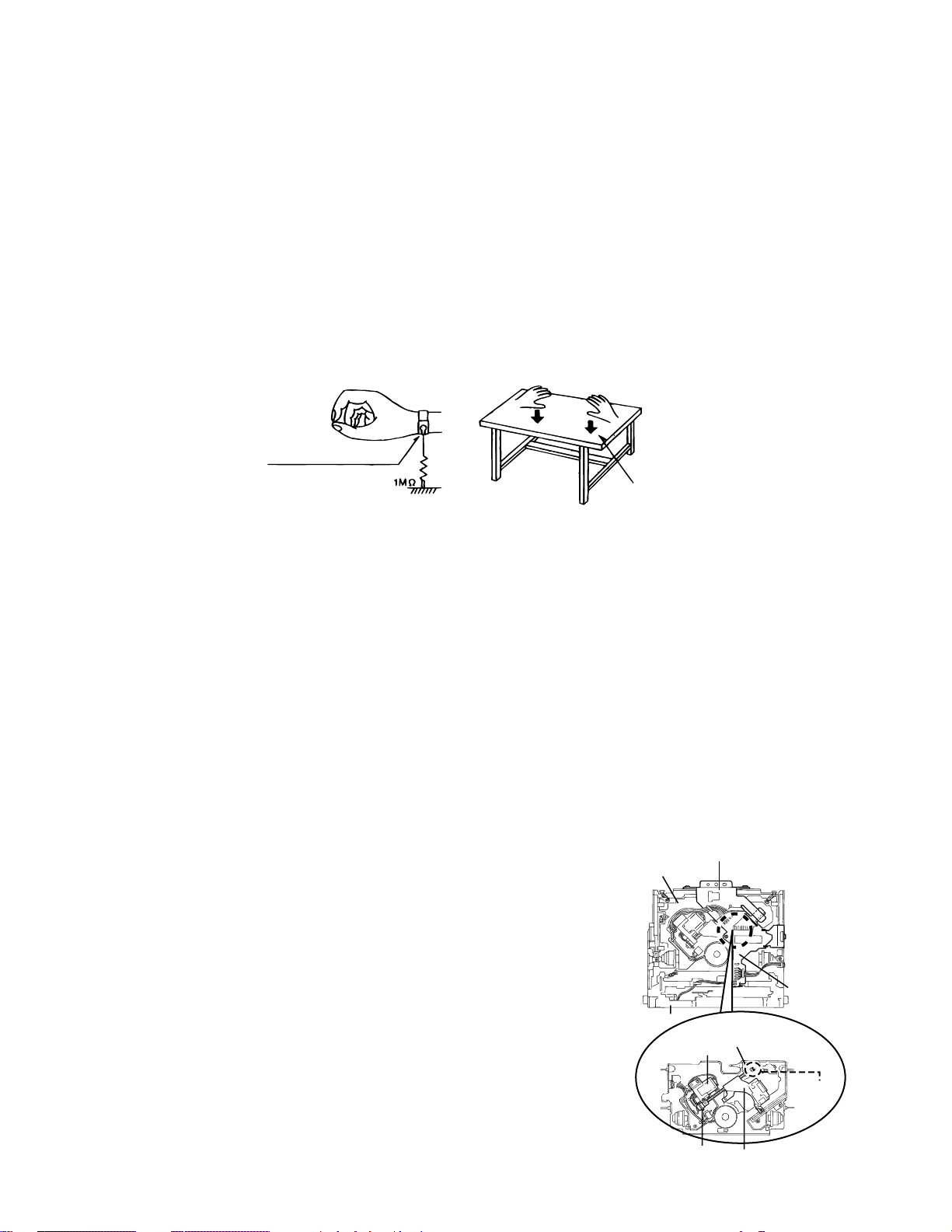
1.Grounding to prevent damage by static electricity
Electrostatic discharge (ESD), which occurs when static electricity stored in the body, fabric, etc. is discharged,
can destroy the laser diode in the traverse unit (optical pickup). Take care to prevent this when performing repairs.
2.About the earth processing for the destruction prevention by static electricity
Static electricity in the work area can destroy the optical pickup (laser diode) in devices such as CD players.
Be careful to use proper grounding in the area where repairs are being performed.
2-1 Ground the workbench
Ground the workbench by laying conductive material (such as a conductive sheet) or an iron plate over
it before placing the traverse unit (optical pickup) on it.
2-2 Ground yourself
Use an anti-static wrist strap to release any static electricity built up in your body.
(caption)
Anti-static wrist strap
Conductive material
3. Handling the optical pickup
1. In order to maintain quality during transport and before installation, both sides of the laser diode on the
replacement optical pickup are shorted. After replacement, return the shorted parts to their original condition.
(Refer to the text.)
2. Do not use a tester to check the condition of the laser diode in the optical pickup. The tester's internal power
source can easily destroy the laser diode.
(conductive sheet) or iron plate
4.Handling the traverse unit (optical pickup)
1. Do not subject the traverse unit (optical pickup) to strong shocks, as it is a sensitive, complex unit.
2. Cut off the shorted part of the flexible cable using nippers, etc. after replacing the optical pickup. For specific
details, refer to the replacement procedure in the text. Remove the anti-static pin when replacing the traverse
unit. Be careful not to take too long a time when attaching it to the connector.
3. Handle the flexible cable carefully as it may break when subjected to strong force.
4. It is not possible to adjust the semi-fixed resistor that adjusts the laser power. Do not turn it
CD mechanism ass’y
Damper bracket
Attention when traverse unit is decomposed
*Please refer to "Disassembly method" in the text for pick-up and how to
detach the substrate.
1.Solder is put up before the card wire is removed from connector on
the CD substrate as shown in Figure.
(When the wire is removed without putting up solder, the CD pick-up
assembly might destroy.)
2.Please remove solder after connecting the card wire with
when you install picking up in the substrate.
Front bracket
Feed motor ass’y
FD screw
CD mechanism
control board
Soldering
FD gear
Pickup unit
1-3
Page 4
KD-S587
Disassembly method
<Main body>
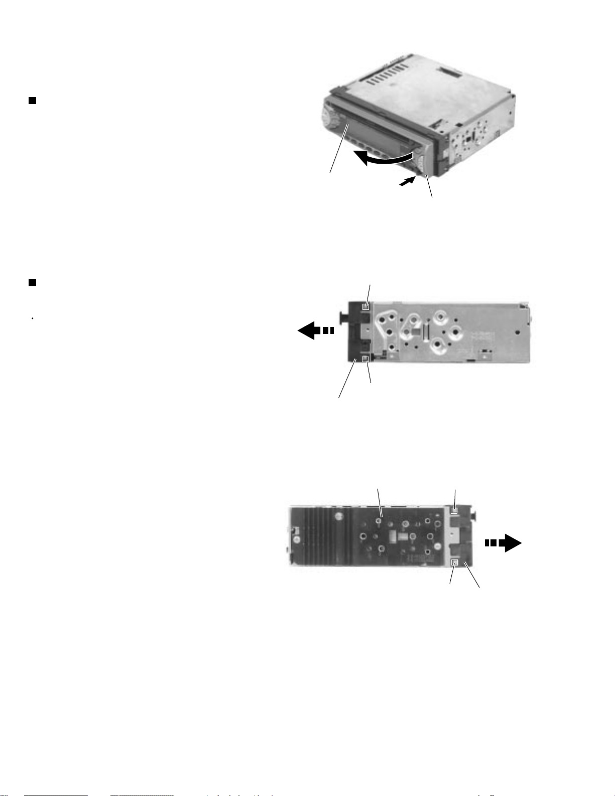
Removing the front panel assembly
(See Fig.1)
1.
Press the eject button in the lower right part of the
front panel. Remove the front panel assembly from
the body.
Front panel assembly
Eject button
Fig.1
Removing the front chassis assembly
(See Fig.2 and 3)
Prior to performing the following procedure, remove
the front panel assembly.
1.
Release the four joint tabs a on both sides of the
front chassis assembly and remove the front chassis
assembly toward the front.
Tab a
Tab a
Front chassis assembly
Heat sink
Fig.2
Tab a
1-4
Fig.3
Tab a
Front chassis
assembly
Page 5
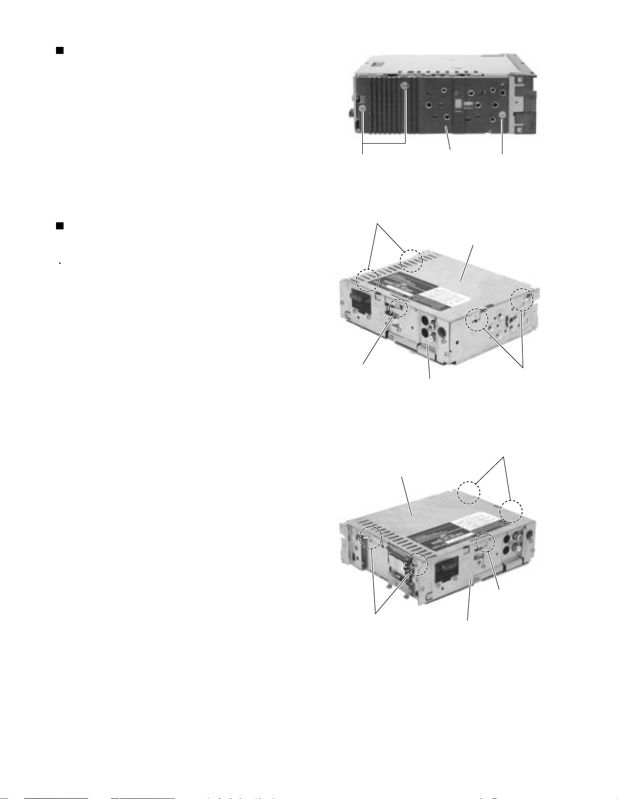
Removing the heat sink (See Fig.4)
1.
Remove the three screws A on the left side of the
body.
KD-S587
Removing the bottom cover
(See Fig.5 and 6)
Prior to performing the following procedure, remove
the front panel assembly, the front chassis assembly
and the heat sink.
1.
Turn over the body and unjoint the five joints b with
the bottom cover and the body using a screwdriver.
A
Joints b
Joint b
Heat sink
Fig.4
Rear panel
Fig.5
A
Bottom cover
Joints b
Bottom cover
Joints b
Joints b
Joint b
Rear panel
Fig.6
1-5
Page 6
KD-S587
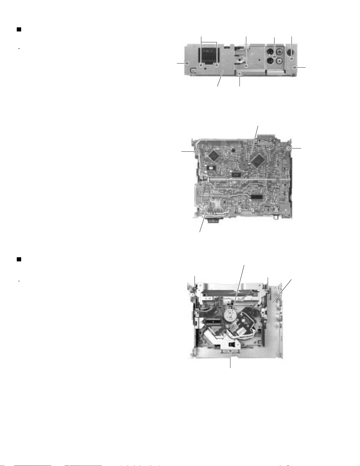
Removing the main board
(See Fig.7 and 8)
Prior to performing the following procedure, remove
the front panel assembly, the front chassis assembly,
the heat sink and the bottom cover.
1.
Remove the screw B, the four screws C and the
three screws D attaching the rear bracket on the
back of the body. Remove the rear panel.
2.
Remove the two screws E attaching the main board
on the bottom of the body. Disconnect connector
CN501 on the main board in the direction of the
arrow.
D
E
Rear panel
CC
D
Fig.7
Main board
B
C
D
E
Removing the CD mechanism section
(See Fig.9)
Prior to performing the following procedure, remove
the front panel assembly, the front chassis assembly,
the heat sink, the bottom cover and the main board.
1.
Remove the three screws F attaching the cassette
mechanism section on the back of the top chassis.
CN501
F
Fig.8
CD mechanism section
F
Fig.9
F
Top chassis
1-6
Page 7
KD-S587
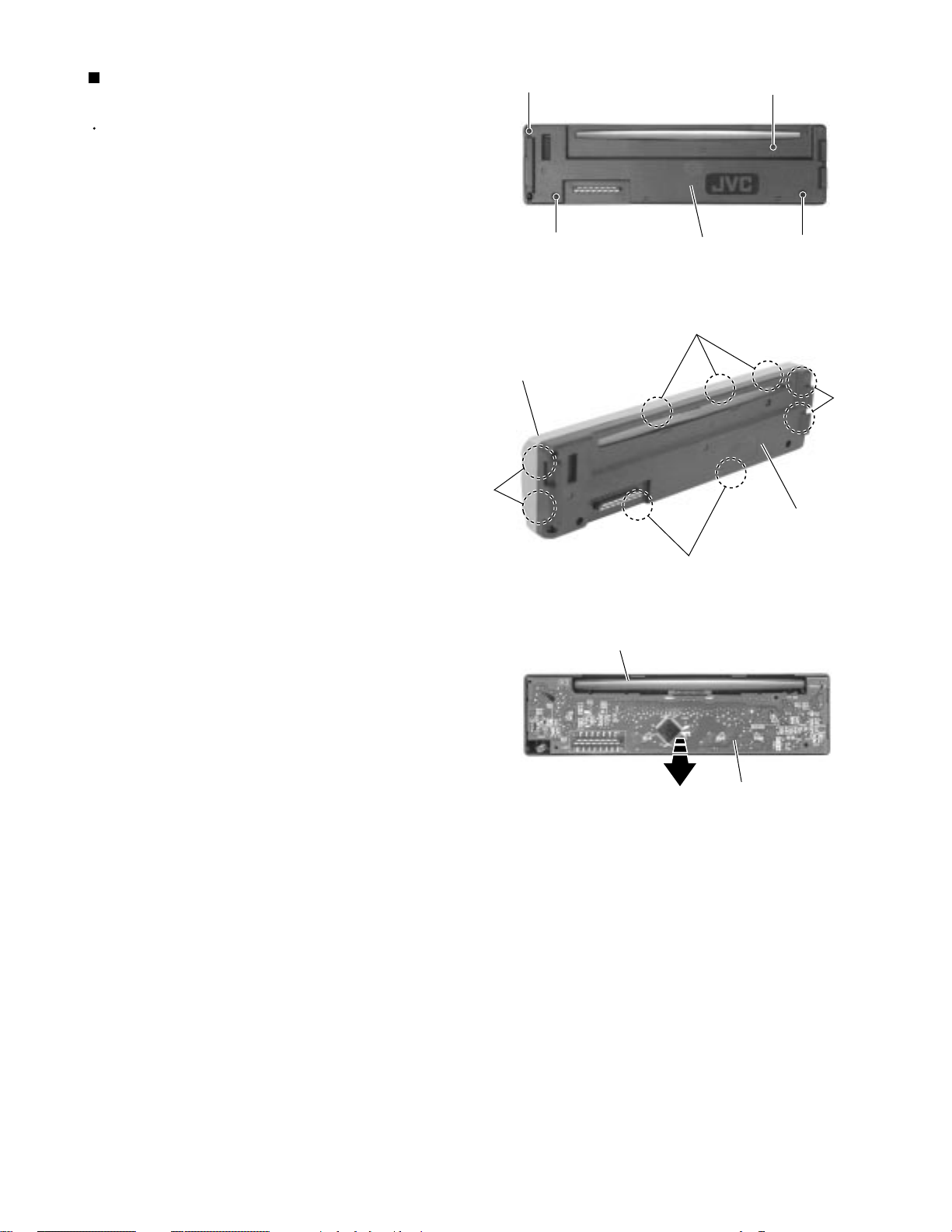
Removing the control switch board
(See Fig.10 to 12)
Prior to performing the following procedure, remove
the front panel assembly.
1.
Remove the four screws G attaching the rear cover
on the back of the front panel assembly.
2.
Unjoint the nine joints c with the front panel and the
rear cover.
3.
Remove the control switch board on the back of the
front panel.
Joints c
G
Front panel
G
Rear cover
Fig.10
Joints c
G
G
Joints c
Rear cover
Front panel
Joints c
Fig.11
Control switch board
Fig.12
1-7
Page 8
KD-S587
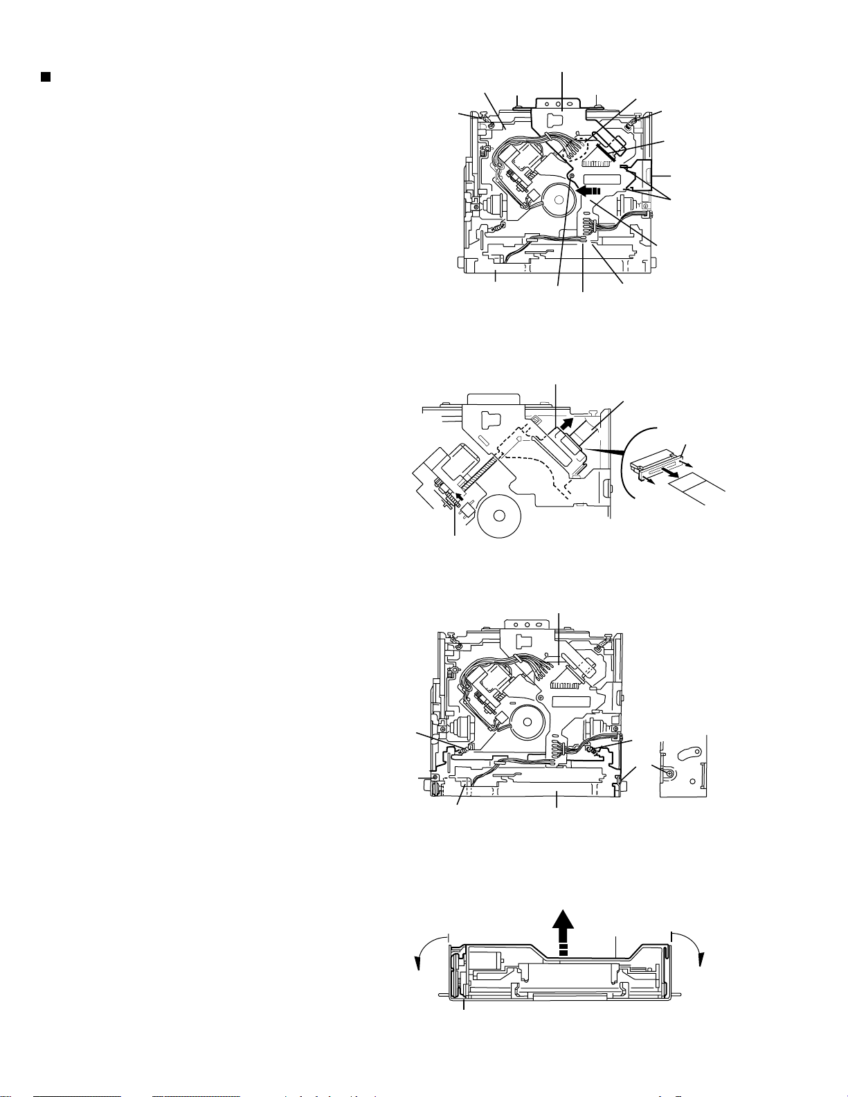
Removing the CD mechanism control
board(See Fig.1 and 2)
Unsolder the part f and g on the CD mechanism
control board.
Remove the stator fixing the CD mechanism control
board and the damper bracket (To remove the stator
smoothly, pick up the center part).
Remove the screw F attaching the CD mechanism
control board.
Remove the CD mechanism control board in the
direction of the arrow while releasing it from the two
damper bracket slots i and the front bracket slot j.
Disconnect the flexible wire from connector on the
pickup unit.
ATTENTION:
Turn the FD gear in the direction of the
arrow to move the entire pickup unit to
the appropriate position where the
flexible wire of the CD mechanism unit
can be disconnected easily (Refer to
Fig.2).
CD mechanism ass’y
m
Front bracket
Damper bracket
I
g
F
Fig.1
Pickup unit
I
j
Flexible wire
f
m
h
I
i
CD mechanism
control board
Shift the lock
FD gear
k
G
Loading motor
Pull outward
Fig.2
CD mechanism control board
Front bracket
Fig.3
Front bracket
k
G
Pull outward
1-8
Flame
Fig.4
Page 9
KD-S587
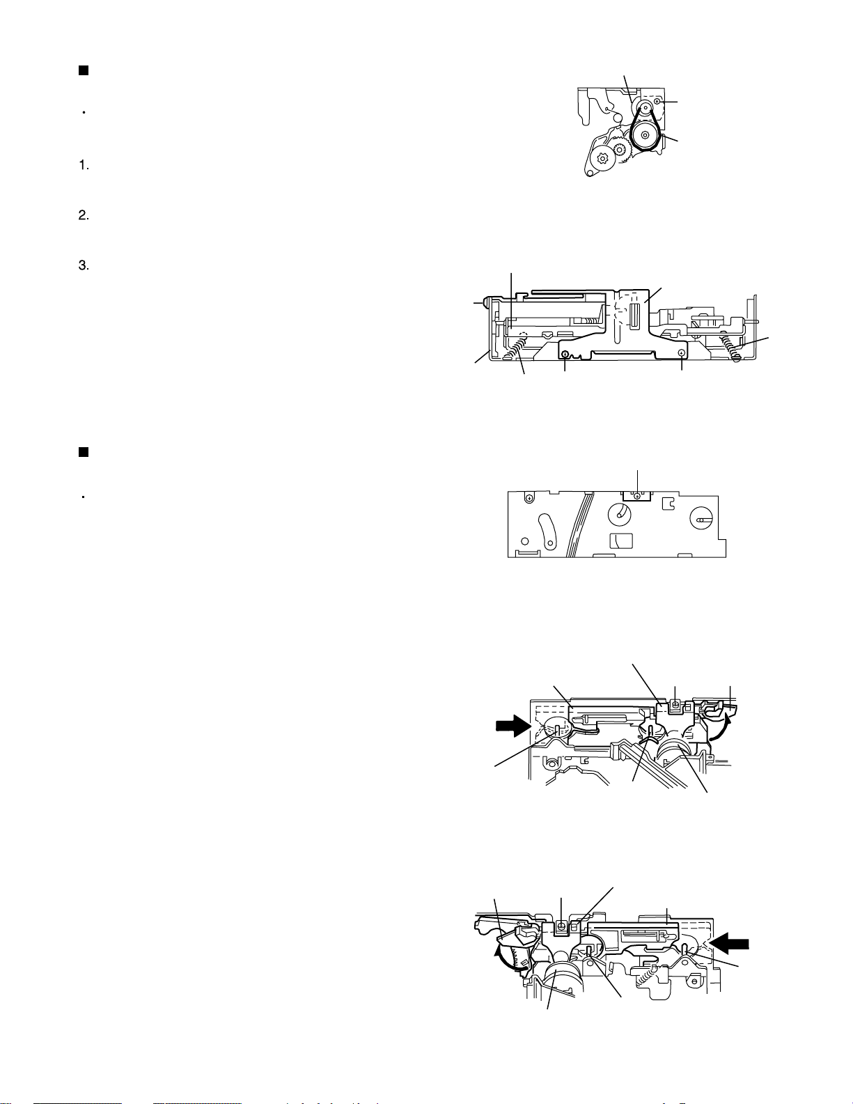
Removing the loading motor
(See Fig.3 to 5)
Prior to performing the following procedure, remove
the CD mechanism control board.
Remove the two springs k attaching the CD mechanism
ass’y and the front bracket.
Remove the two screws G and the front bracket
while pulling the flame outward.
Remove the belt and the screw H from the loading
motor.
Removing the CD mechanism ass’y
(See Fig.1, 6 to 9)
CD mechanism ass’y
I
Flame
Loading motor
m
H
Belt
Fig.5
Damper bracket
m
I
Fig.6
I
I
Prior to performing the following procedure, remove
the CD mechanism control PWB and the front
bracket (loading motor).
1.
Remove the three screws I and the damper bracket.
2.
Raise the both sides fix arms and move the fix plates
in the direction of the arrow to place the four shafts l
as shown in Fig.8 and 9.
3.
Remove the CD mechanism ass’y and the two
springs m attaching the flame.
4.
Remove the two screws J and both sides rear
damper brackets from the dampers. Detach the CD
mechanism ass’y from the left side to the right side.
ATTENTION:
The CD mechanism ass’y can be
removed if only the rear damper
bracket on the left side is removed.
Fix plate (L)
l
Fix arm (R)
Fig.7
Rear damper bracket
l
Fig.8
Rear damper bracket
J
Fix plate(R)
J
Fix arm (L)
Damper
Damper
l
l
Fig.9
1-9
Page 10

KD-S587
Removing the feed motor ass’y
(See Fig.10)
Prior to performing the following procedure, remove
the CD mechanism control board, the front bracket
(loading motor) and the CD mechanism ass’y.
1.
Remove the two screws K and the feed motor ass’y.
Removing the pickup unit
(See Fig.10 and 11)
*Prior to performing the following procedure, remove
the CD mechanism control board, the front bracket
(loading motor), the CD mechanism ass’y and the
feed motor ass’y.
1.
Detach the FD gear part of the pickup unit upward.
Then remove the pickup unit while pulling out the
part n of the FD screw.
Feed motor ass’y
K
FD gear
Nut push spring plate
FD screw
Pickup unit
Fig.10
Part n
Part O
Pickup unit
L
Pickup mount nut
Pickup unit
ATTENTION:
2.
Remove the screw L attaching the nut push spring
plate and the pickup mount nut from the pickup unit.
Pull out the FD screw.
When reattaching the pickuap unit,
reattach the part o of the pickup unit,
then the part n of the FD screw.
Removing the spindle motor
(See Fig.12 and 13)
Prior to performing the following procedure, remove
the CD mechanism control board, the front bracket
(loading motor), the CD mechanism ass’y and the
feed motor ass’y.
1.
Turn up the CD mechanism ass’y and remove the
two springs p on both sides of the clamper arms.
Open the clamper arm upward.
2.
Turn the turn table, and remove the two screws M
and the spindle motor.
FD screw
p
Spindle motor
Fig.11
p
Fig.12
M
1-10
M
Fig.13
Page 11

Adjustment method
KD-S587
Test instruments required for adjustment
1. Digital oscilloscope (100MHz)
2. AM Standard signal generator
3. FM Standard signal generator
4. Stereo modulator
5. Electric voltmeter
6. Digital tester
7. Tracking offset meter
8. Test Disc JVC :CTS-1000
9. Extension cable for check
EXTGS004-26P 1
Standard measuring conditions
Power supply voltage DC14.4V(10.5~16V)
Load impedance 4 (2 Speakers connection)
Line out load impedance 20k
Output Level Line out 2.0V (Vol. MAX)
How to connect the extension cable for adjusting
Standard volume position
Balance and Bass &Treble volume : lndication"0"
Loudness : OFF
Frequency Band
FM 87.5MHz ~ 108.0MHz
AM 531kHz ~ 1620 kHz
Dummy load
Exclusive dummy load should be used for AM,and FM. For
FM dummy load,there is a loss of 6dB between SSG output
and antenna input.The loss of 6dB need not be considered
since direct reading of figures are applied in this working
standard.
The cardboard is cut in a suitable size.
uses for the insulation stand of mechanism.
EXTGS004-26P
1-11
Page 12

KD-S587
Flow of functional operation until TOC read
Power ON
• When the pickup correctly moves
to the inner area of the disc
Set Function to CD
• When the laser diode correctly
emits
Microprocessor
commands
FMO
TC9462 "53"
FEED MOTOR
+TERMINAL
TERMINAL
IC581 "5"
REST SW
• When correctly focused
Focus Servo Loop ON
Disc inserted
Pickup feed to the inner area
Laser emitted
Focus search
Disc rotates
RF signal eye-pattern
remains closed
Tracking loop closed
RF signal eye-pattern
opens
TOC readout
YES
YES
Microprocessor
commands
"No disc"
display
• When the disc correctly rotates
Microprocessor
commands
Spindle
motor (-)
IC581 "7"
AccelerationAcceleration
0.5 Sec
Rough
Servo
0.5 Sec
Servo CLV
1-12
Jump to the first track
Play
Tracking Servo Loop ON
• RF signal
Rough Servo Mode
CLV Servo Mode
(ProgramArea)
CLV Servo Mode
(Lead-In Area;
Digital: 0)
Page 13

Feed Section
Is the voltage output at
IC521 pin "53" 5V or 0V?
YES
Is 4V present at both
sides of the feed motor?
YES
NO
Is the wiring for IC521
(90) ~ (100) correct?
NO
Is 6V or 2V present at
IC581 "5" and "6"?
NO
YES
YES
Is 5V present at IC581
pin "11"?
YES
Check the vicinity of
IC521.
Check the feed motor
connection wiring.
NONO
KD-S587
Check CD 9V
and 5V.
Check the feed motor.
Focus Section
When the lens is
moving:
4V
Does the S-search
waveform appear at
IC581 pins "17" and "18"?
Spindle Section
Is the disk rotated?
YES
Does the RF signal
appear at TP1?
YES
Check IC581.
NO
YES
NO
NO
Check the circuits in
the vicinity of IC581
pins "15" ~ "18".
Check the pickup and
its connections.
Is 4V present at IC581
pins "7" and "8" ?
Check the spindle motor
and its wiring.
YES
YES
NO NO
Is 4V present at IC521
pin "55" ?
YES
Check the vicinity of
IC581.
Check IC501 and
IC521.
Is the RF waveform at TP1
distorted?
YES
Proceed to the Tracking
section
Tracking Section
When the disc is rotated
at first:
Is the tracking error signal
output at IC501 "12"?
Check IC521.
NO
Approx. 1.2 V
YES
Check the circuits in the
vicinity of IC501 "19" ~
"24" or the pickup
Check the circuit in the
vicinity of IC501 pins
"2" ~ "12".
YESYES
Check the pickup and
its connections.
1-13
Page 14

KD-S587
Maintenance of laser pickup
(1) Cleaning the pick up lens
Before you replace the pick up, please try to
clean the lens with a alcohol soaked cotton
swab.
(2) Life of the laser diode
When the life of the laser diode has expired,
the following symptoms will appear.
(1) The level of RF output (EFM output:ampli
tude of eye pattern) will be low.
Is RF output
1.0 0.35Vp-p?
YES
O.K
(3) Semi-fixed resistor on the APC PC board
The semi-fixed resistor on the APC printed
circuit board which is attached to the pickup
is used to adjust the laser power.Since this
adjustment should be performed to match the
characteristics of the whole optical block,
do not touch the semi-fixed resistor.
If the laser power is lower than the specified
value,the laser diode is almost worn out, and
the laser pickup should be replaced.
If the semi-fixed resistor is adjusted while
the pickup is functioning normally,the laser
pickup may be damaged due to excessive current.
NO
Replace it.
Replacement of laser pickup
Turn off the power switch and,disconnect the
power cord from the ac outlet.
Replace the pickup with a normal one.(Refer
to "Pickup Removal" on the previous page)
Plug the power cord in,and turn the power on.
At this time,check that the laser emits for
about 3seconds and the objective lens moves
up and down.
Note: Do not observe the laser beam directly.
1-14
Play a disc.
Check the eye-pattern at TP1.
Finish.
Page 15

Description of major ICs
LC75823W (IC601) : LCD driver
1. Pin Layout & Symbol
KD-S587
S1
S2
S3
S4
S5
S6
S7
S8
S9
S10
S11
S12
S13
S14
S15
S16
2. Pin Function
DICLCE
64 63 62 61 60 59 58 57 56 55 54 53 52 51 50 49
1
2
3
4
5
6
7
8
9
10
11
12
13
14
15
16
17 18 19 20 21 22 23 24 25 26 27 28 29 30 31 32
S17
S18
S19
OSC
S20
Vss
S21
VDD2
VDD1
S22
S23
INH
S24
VDD
S25
COM3
COM2
S26
S27
COM1
S52
S28
S29
S51
S30
S50
S31
S49
48
47
46
45
44
43
42
41
40
39
38
37
36
35
34
33
S32
S48
S47
S46
S45
S44
S43
S42
S41
S40
S39
S38
S37
S36
S35
S34
S33
Pin No.
1 to 52
53 to 55
56
57
58
59
60
61
62
63
Symbol
S1 to S52
COM1 to COM3
VDD
INH
VDD1
VDD2
Vss
OSC
CE
CL
I/O
O
Segment output pins used to display data transferred
Function
by serial data input.
O
Common driver output pins. The frame frequency is given
by : t0=(fosc/384)Hz.
--
Power supply connection. Provide a voltage of between
4.5 and 6.0V.
I
Display turning off input pin.
INT="L" (Vss) ----- off (S1 to S52, COM1 to COM3="L"
INT="H" (VDD)----- on
Serial data can be transferred in display off mode.
I
Used for applying the LCD drive 2/3 bias voltage
externally.
Must be connected to VDD2 when a 1/2 bias drive scheme
is used.
I
Used for applying the LCD drive 1/3 bias voltage
externally.
Must be connected to VDD1 when a 1/2 bias drive scheme
is used.
--
Power supply connection. Connect to GND.
I/O
Oscillator connection.
An oscillator circuit is formed by connecting an external
resistor and capacitor at this pin.
Serial data CE : Chip enable
interface connection
I
to the controller. CL : Sync clock
64
DI
DI : Transfer data
1-15
Page 16

KD-S587
AN8806SB-W (IC501) : RF & Servo amp.
1.Pin layout
PD
LD
LDON
LDP
VCC
RF-
RF OUT
RF IN
C.AGC
ARF
C.ENV
C.EA
CS BDO
BDO
CS BRT
OFTR
/NRFDET
GND
1
2
3
4
5
6
7
8
9
10
11
12
13
14
15
16
17
18
36
35
34
33
32
31
30
29
28
27
26
25
24
23
22
21
20
19
PDAC
PDBD
PDF
PDE
PDER
PDFR
TBAL
FBAL
EF EF OUT
TE TE OUT
CROSS
TE BPF
VDET
LD OFF
VREF
ENV
2.Block diagram
36
-+
35
-+
31
34
-+
32
33
-+
6
--
VCBA
+
29
728
-+
--
+
+
VCBA
--
+
VCBA
--
--
VCBA
+
+
--
-+
-+
+
--
27
-+
--
EQ
+
+
--
+
--
910 17
8
AGC
OFTR
BDO
RF
DET
11
12 19
ENV CURCUIT
13
14
15
16
-+
20
21
2
1-16
24 25
30
14
23
26
22
3
Page 17

3. Pin function
KD-S587
Pin No.
1
2
3
4
5
6
7
8
9
10
11
12
13
14
15
16
17
18
19
20
21
22
23
24
25
26
27
28
29
30
31
32
33
34
35
36
Symbol
PD
LD
LD ON
LDP
VCC
RF-
RF OUT
RF IN
C.AGC
ARF
C.ENV
C.EA
CS BDO
BDO
CS BRT
OFTR
/NRFDET
GND
ENV
VREF
LD OFF
VDET
TE BPF
CROSS
TE OUT
TE-
FE OUT
FE-
FBAL
TBAL
PDFR
PDER
PDF
PDE
PD BD
PD AC
I/O
I
APC amp input terminal
APC amp output terminal
O
APC ON/OFF control terminal
I
--
Connect to ground
Power supply
--
Inverse input pin for RF amp
I
RFamp output
O
RF input
I
Connecting pin of AGC loop filter
I/O
RF output
O
I/O
A capacitor is connected to this terminal to detect the envelope of RF signal
I/O
A capacitor is connected to this terminal to detect the envelope of RF signal
A capacitor is connected to detect the lower envelope of RF signal
I/O
BDO output pin
O
A capacitor is connected to detect the lower envelope of RF signal
I/O
O
Of-track status signal output
RF detection signal output
O
--
Ground
O
Envelope output
Reference voltage output
O
--
Connect to ground
O
Vibration detection signal output
I
Input pin of tracking error through BPF
O
Tracking error cross output
O
Tracking error signal output
Inverse input pin for tracking error amp
I
O
Output pin of focus error
Inverse input pin for focus error amp
I
I
Focus balance control
I
Tracking balance control
F I-V amp gain control
I/O
E I-V amp gain control
I/O
I
I-V amp input
I-V amp input
I
I
I-V amp input
Description
I I-V amp input
1-17
Page 18

KD-S587
LA4743K (IC321) : Power amp
1.Block diagram
IN 1
TA B
IN 2
+
0.22 F
+
0.22 F
11
1
12
Vcc 1/2 Vcc 3/4
6 20
-
+
Protective
circuit
-
+
2200 F 0.022 F
+
9
7
+
OUT 1+
OUT 1-
PWR GND1
8
+
OUT 2+
5
-
OUT 2-
3
PWR GND2
2
ST BY
R.F
47 F
IN 3
PRE GND
IN 4
+5V
ST ON
+
0.22 F
N.C
+
0.22 F
4
Stand by
Switch
Mute
10
+
Ripple
Filter
Mute
22
circuit
3.3 F
+
15
-
+
-
17
19
10K
+
OUT 3+
OUT 3-
Low Level
Mute ON
25
18
21
23
PWR GND3
OUT 4+
OUT 4-
13
14
Protective
circuit
-
+
+
-
1-18
ON TIME C
22 F
Muting &
16
+
ON Time Control
Circuit
PWR GND4
24
Page 19

2.Pin layout
3.Pin function
1
2
3
4
5
6
7
8
9
10
11
12
13
14
15
16
17
18
19
20
21
22
23
24
25
SymbolPin No. Function
TA B
GND
RFOSTBY
RFO+
VCC1/2
RROGND
RRO+
VREF
RRIN
RFIN
SGND
LFIN
LRIN
ONTIME
LRO+
GND
LROVCC3/4
LFO+
MUTE
LFO-GND
NC
Header of IC
Power GND
Outpur(-) for front Rch
Stand by input
Output (+) for front Rch
Power input
Output (-) for rear Rch
Power GND
Output (+) for rear Rch
Ripple filter
Rear Rch input
Front Rch input
Signal GND
Front Lch input
Rear Lch input
Power on time control
Output (+) for rear Lch
Power GND
Output (-) for rear Lch
Power input
Output (+) for front
Muting control input
Output (-) for front
Power GND
No connection
KD-S587
1-19
Page 20

KD-S587
LA6567H-X (IC541) : CD driver
1.Pin layout & Blockdiagram
VCC2
V05-
V05+
V04+
V04-
V03+
V03-
FR
1
2
3
4
5
6
7
FR
CH 3,4,5
Power supply
CH5
CH4
CH3
Thermal shutdown
Output control
Level shiftLevel shiftLevel shiftLevel shift
Input
22K 11K
Signal system power supply
28
27
26
25
24
23
22
FR
REV
FWD
S-GND
VCONT
VIN4
VIN4G
VCC-S
FR
V02+
V02-
V01+
V01-
VCC1
VIN1
VIN1G
8
9
10
11
12
13
14
CH2
CH1
CH1,2
Power supply
11K
22K
5VREG(PNPTr
The outside putting)
22K
11K
22K
11K
21
20
19
18
17
16
15
VREF-IN
REG-OUT
REG-IN
VIN3G
VIN3
VIN2G
VIN2
1-20
Page 21

2. Pin function
KD-S587
Pin no. Symbol
1
2
3
4
5
6
7
8
9
10
11
12
13
14
15
16
17
18
19
20
21
22
23
24
25
26
27
VCC2
V05V05+
V04+
V04V03+
V03V02+
V02V01+
V01-
VCC1
VIN1
VIN1G
VIN2
VIN2G
VIN3
VIN3G
REG-IN
REG-OUT
VREF-IN
VCC-S
VIN4G
VIN4
VCONT
S-GND
FWD
Function
CH3,4,5 Power supply( It is short with VCC1,VCC-S)
Loading output(-)
Loading terminal (+)
CH4 Output terminal(+)
CH4 Output terminal(-)
CH3 Output terminal(+)
CH3 Output terminal(-)
CH2 Output terminal(+)
CH2 Output terminal(-)
CH1 Output terminal(+)
CH1 Output terminal(-)
CH1,2(BTL) Power supply(It is short with VCC-S,VCC2)
CH1 Input terminal
CH1 Input terminal(For gain adjustment)
CH2 Input terminal
CH2 Input terminal(For gain adjustment)
CH3 Input terminal
CH3 Input terminal(For gain adjustment)
Regulator terminal(Outside putting PNP base)
Regulator terminal(Outside putting PNP collector)
Standard voltage input terminal
Signal system power supply(It is short with VCC1,VCC2)
CH4 Input terminal(For gain adjustment)
CH4 Input terminal
5CH(VLO) Output voltage set terminal
Signal system GND
5CH(VLO)Signal output switch terminal(FWD),Input of logic of loading part
28
Frame(FR)at the center becomes system GND.
Please be short-circuited on the outside and use the terminal of the power supply system
and three teminals of VCC-S, VCC1,VCC2.
REV
5CH(VLO)Signal output switch terminal(REV),
Input of logic of loading part
1-21
Page 22

KD-S587
LC72366-9A73 (IC801) : System CPU
1. Pin layout
25
~
40
2. Pin function
1
2
3
4
5
6
7
8
9
10
11
12
13
14
15
16
17
18
19
20
21
22
23
24
25
26
27
28
29
30
31
32
33
34
35
36
37
38
39
40
J-BUS SCK
DIMMER OUT
CD LSI RESET
24 ~ 1
41 ~ 64
Symbol FunctionPin No.
XIN
TEST2
J-BUS SI
J-BUS SO
J-BUS I/O
SUBQ
SQCK
RESET
LCD SI
LCD SO
LCD SCK
LCD CE
FM ILLUMI
AM ILLUMI
CD ILLUMI
LM0
LM1
KS2
KS1
KS0
DETACH
K2
K1
K0
Vdd
SW2
MCLK
M DATA
MLD
SCL
SDA
80
65
~
I/O
I
Crystal oscillator input port
I
Connect to ground
-
No use
-
No use
-
No use
-
No use
I/O
CD LSI subcode data input
-
No use
I/O
CD LSI subcode clock
I
Micon reset pin
-
No use
O
LCD driver data output
O
LCD driver clock signal
O
LCD driver chip enable port
-
No use
-
No use
-
No use
-
No use
O
CD loading motor output
O
CD loading motor output
-
No use
-
No use
-
No use
O
Output for initial setting diode matrix
O
Output for initial setting diode matrix
O
Output for initial setting diode matrix
I
Front panel detect
-
No use
I
Input for initial setting diode matrix
I
Input for initial setting diode matrix
-
5V power supply port (+B)
I
CD mechanism detect switch
O
CD LSI reset
O
CD LSI command clock signal
O
CD LSI command data output
O
CD LSI command load signal
-
No use
-
No use
O
E.volume clock output
O
E.volume data output
1-22
Page 23

41
42
43
44
45
46
47
48
49
50
51
52
53
54
55
56
57
58
59
60
61
62
63
KEY CHANGE
64
65
66
67
68
69
70
FM IF COUNT
71
72
73
74
75
76
77
78
79
80
CD ON
RELAY
BLKCK
BEEP
SW4
SW1
SW3
REST
FLOCK
TLOCK
CD SENSE
STATUS
P.SAVES2
SD/ST
REMOCON
J BUS INT
BAND
MONO
IFRQ/AGC
MUTE
LEVEL
S.METER
KEY2
KEY1
KEY0
P.SAVE1
SENSE
NC
NC
Vdd
AM OSC
FM OSC
VSS
NC
E0
TEST1
XOUT
I/OPort Name FunctionPin No.
CD 8V supply on
5V power contorl
Sub-code/block/clock signal output
I
No use
CD mechanism detect switch
I
CD mechanism detect switch
I
CD mechanism detect switch
I
CD pickup rest position
I
Focus lock signal output Active:Low
I
Tracking lock signal output Active :low
I
CD LSI sense signal
I
CD LDI status signal
I
power save 2:+B detect
I
Station detection,Stereo signal input H:SD
I
Remocon input
I
No use
FM/AM band selection
O
FM mono selection
During FM auto search,IF request output H after SD detected. During AM
O
auto search,AGC output
Muting switch
O
Level meter input
I
S meter input
I
Control to GND
Key 2 input port
I
Key 1 input port
I
Key 0 input port
I
Power save 1,ACC power detection
I
Voltage sensor port
I
No use
FM frequency detecting
I
No use
No use
5V power supply (+B)
No use
I
FM limited signal input
I
Ground port for power supply
No use
Error signal output port for PLL
O
Test port for LSI, To connect ground
-
4.5MHz crystal oscillator output
O
KD-S587
1-23
Page 24

KD-S587
MN6627482WA (IC561) : Digital servo & Digital signal processer D/A converter
1. Pin layout
2.Block diagram
LRCKIN(MSEL)
BCLK(SSEL)
SRDATAIN
(PSEL)
IOSEL
CLVS
CRC
BLKCK
CLDCK
SBCK
SUBC
DEMPH
RESY
FLAG6(RESY)
SSEL
SQCK
SUBQ
AVDD2
AVDD2
PCK
EFM
PLLF
DSLF
IREF
DRF
ARF
RSEL
PSEL
MLD
MCLK
MDATA
CK384(EFM)
VCOF
BYTCK
SMCK
FCLK
CSEL
MSEL
X2
X1
ÊSTAT
DIGITAL
DEEMPHSIS
SUB
CODE
BUFFER
DSL.
PLL
VCO
VCO
ITUNING
GENERATION
PITCH
CONTROL
20 ~ 1
21
~
40
41 ~ 60
8TIMES
OVER SAMPUNC
DIGITAL FILTER
EFM
DEMODULATION
SYNC
INTERPOLATION
SUBCODE
DEMODULATION
MICRO
COMPUTER
INTERFACE
COVERTER
A/D
80
~
61
CIRC
ERROR
CORRECTION
DEINTERLEVE
CLV
SERVO
1BIT
DAC
LOGIC
S
16k
SRAM
INPUT
PEM
(R)
PEM
(L)
D/A
CONVERTER
OUTPUT
DIGITAL
AUDIO
INTERFASE
DIGITAL
AUDIO
INTERFASE
INTER POLATION
SOFT MUTING DIGITAL
ATTENUATION
PEAK DETECTIVE
AUTO CUE
PORT
SERVO
TIMING GENERATOR
AVSS1
AVDD1
OUTR
OUTL
FLAG
IPFLAG
TX
ECM
PC
LRCK
SRDATA
BCLK
DMUTE
TRKV
KICK
VREF
TRVSTR
ECS
TVD
TRD
FOD
TBAL
FBAL
TOFS
TES
/TLOCK
/FLOCK
PLAY
LDON
WVEL
SENSE
1-24
D
/
D
V
V
V
S
D
D
S
D
D
1
/
R
V
T
S
S
E
T
S
S
1
T
F
E
R
T
F
E
E
N
V
T
R
C
R
S
B
V
D
D
O
E
T
/
R
F
D
E
O
F
T
Page 25

3. Pin function
Pin
No.
1
2
3
4
5
6
7
8
9
10
11
12
13
14
15
16
17
18
19
20
21
22
23
24
25
26
27
28
29
30
31
32
33
34
35
36
37
38
39
40
Symbol
BCLK
LRCK
SRDATA
DVDD1
DVSS1
TX
MCLK
MDATA
MLD
SENSE
FLOCK
TLOCK
BLKCK
SQCK
SUBQ
DMUTE
STAT
RST
SMCK
PMCK
TRV
TVD
PC
ECM
ECS
KICK
TRD
FOD
VREF
FBAL
TBAL
FE
TE
RF ENV
VDET
OFT
TRCRS
RFDET
BDO
LDON
I/O
O
O
O
O
I
I
I
O
O
O
O
I
O
O
I
O
O
O
O
O
O
O
O
O
O
Function
Not used
Not used
Not used
I
Power supply (Digital)
I
Connected to GND
Not used
CPU command clock signal input
(Data is latched at signal's rising point)
CPU command data input
CPU command load signal input
Sense signal output
Focus lock signal output Active :Low
Tracking lock signal output Active :Low
sub-code/block/clock signal output
Outside clock for sub-code Q resister input
Sub-code Q -code output
I
Connected to GND
Status signal
(CRC,CUE,CLVS,TTSTOP,ECLV,SQOK)
Reset signal input (L:Reset)
I
Not used
I
Not used
Traverse enforced output
Traverse drive output
I
Not used
Spindle motor drive signal (Enforced
mode output) 3-State
Spindle motor drive signal (Servo error
signal output)
Kick pulse output
Tracking drive output
Focus drive output
Reference voltage input pin for D/A
I
output block (TVD,FOD,FBA,TBAL)
Focus Balance adjust signal output
Tracking Balance adjust signal output
Focus error signal input (Analog input)
I
Tracking error signal input (Analog input)
I
I
RF envelope signal input (Analog input)
Vibration detect signal input (H:detect)
I
Off track signal input (H:off track)
I
Track cross signal input
I
RF detect signal input (L:detect)
I
BDO input pin (L:detect)
I
Laser ON signal output (H:on)
Pin
No.
41
42
43
44
45
46
47
48
49
50
51
52
53
54
55
56
57
58
59
60
61
62
63
64
65
66
67
68
69
70
71
72
73
74
75
76
77
78
79
80
Symbol
TES
PLAY
WVEL
ARF
IREF
DRF
DSLF
PLLF
VCOF
AVDD2
AVSS2
EFM
PCK
PDO
SUBC
SBCK
VSS
XI
X2
VDD
BYTCK
CLOCK
FLAG
IPPLAG
FLAG
CLVS
CRC
DEMPH
RESY
IOSEL
TEST
AVDD1
OUT L
AVSS1
OUT R
RSEL
CSEL
PSEL
MSEL
SSEL
I/O
Tracking error shunt signal output (H:shunt)
O
I
Not used
I
Not used
I
RF signal input
Reference current input pin
I
Bias pin for DSL
I
I/O
Loop filter pin for DSL
Loop filter pin for PLL
I/O
I
Not used
I
Power supply (Analog)
Connected to GND (Analog)
Not used
II I
Not used
I
PLL data slice output
I
Not used
I
Not used
Connected to GND (for X'tal oscillation
I
circuit)
Input of 16.9344MHz X'tal oscillation circuit
I
Output of X'tal oscillation circuit
O
I
Power supply (for X'tal oscillation circuit)
I
Not used
I
Not used
I
Not used
I
Not used
I
Not used
I
Not used
I
Not used
Not used
I
Not used
III
pull up
pull up
Power supply (Digital)
Lch audio output
O
I
Connected to GND
Rch audio output
O
II
pull up
Connected to GND
I
Connected to GND
I
Connected to GND
I
Pull up
Function
KD-S587
1-25
Page 26

KD-S587
HA13164A(IC901):Regulator
1.Terminal layout
123456789101112131415
2.Block diagram
ANT OUT
C3
0.1u
EXT OUT
C4
0.1u
ANT CTRL
CTRL
CD OUT
C5
0.1u
AUDIO OUT
C6
10u
11
12
10
BATT.DET OUT
9
COMPOUT
6
VDD OUT
4
SW5VOUT
5
14
UNIT R:
+B
ACC
ILMOUT
R1
C7
0.1u
C8
0.1u
C1
100u
VCC ACC
8
2
1
7
Surge Protector
BIAS TSD
15
3
TA B
note1) TAB (header of IC)
connected to GND
ILM AJGND GND
13
C2
0.1u
C:F
1-26
3.Pin function
Pin No. Symbol Function
1
2
EXTOUT
ANTOUT
Output voltage is VCC-1 V when M or H level applied to CTRL pin.
Output voltage is VCC-1 V when M or H level to CTRL pin and H level
to ANT-CTRL.
3
4
5
6
7
8
9
10
11
12
13
14
15
ACCIN
VDDOUT
SW5VOUT
COMPOUT
ANT CTRL
VCC
BATT DET
AUDIO OUT
CTRL
CD OUT
ILM AJ
ILM OUT
GND
Connected to ACC.
Regular 5.7V.
Output voltage is 5V when M or H level applied to CTRL pin.
Output for ACC detector.
L:ANT output OFF , H:ANT output ON
Connected to VCC.
Low battery detect.
Output voltage is 9V when M or H level applied to CTRL pin.
L:BIAS OFF, M:BIAS ON, H:CD ON
Output voltage is 8V when H level applied to CTRL pin.
Adjustment pin for ILM output voltage.
Output voltage is 10V when M or H level applied to CTRL pin.
Connected to GND.
Page 27

TEA6320T-X (IC301) : E.volume
1.Pin layout
2.Block diagram
10 8 9 7 6
KD-S587
5
12
SDA
1
GND
2
OUTLR
OUTLF
MUTE
TL
B2L
B1L
IVL
ILL
QSL
IDL
ICL
IMD
IBL
IAL
3
4
5
6
7
8
9
10
11
12
13
14
15
16
3.Pin functions
Pin
Symbol
No.
SDA
1
SCL
32
VCC
31
OUTRR
30
OUTRF
29
TR
28
B2R
27
B1R
26
IVR
25
ILR
24
QSR
23
IDR
22
Vref
21
ICR
CD-CH
TAPE
TUNER
20
19
18
17
CAP
IBR
IAR
I/O
Serial data input/output.
I/O
MUTE
21
31
2
19
16
15
13
11
14
22
20
18
17
Functions Functions
POWER
SUPPLY
SOURCE
SELECTOR
23 25 24 26 27 28
VOLUME 1
+20 to -31 dB
LOUDNESS
LEFT
VOLUME 1
+20 to -31 dB
LOUDNESS
RIGHT
Pin
No.
17
Symbol
IAR
BASS
LEFT
+15 dB
LOGIC
BASS
RIGHT
+15 dB
I/O
I
Input A right source.
TREBLE
LEFT
+12 dB
TREBLE
RIGHT
+12 dB
FUNCTION
ZERO CROSS
DETECTOR
VOLUME 2
0 to 55 dB
BALANCE
FENDER REAR
VOLUME 2
0 to 55 dB
BALANCE
FENDER FRONT
HC BUS
REC
VOLUME 2
0 to -55dB
BALANCE
FENDER FRONT
VOLUME 2
0 to -55dB
BALANCE
FENDER REAR
3
4
32
1
29
30
2
3
4
5
6
7
8
9
10
11
12
13
14
15
16
GND
OUTLR
OUTLF
TL
B2L
B1L
IVL
ILL
QSL
IDL
MUTE
ICL
IMO
IBL
IAL
Ground.
-
output left rear.
O
output left front.
O
Treble control capacitor left channel or
I
input from an external equalizer.
Bass control capacitor left channel or
-
output to an external equalizer.
Bass control capacitor left channel.
-
Input volume 1. left control part.
I
Input loudness. left control part.
I
Output source selector. left channel.
O
Not used
-
Not used
-
Input C left source.
I
Not used
-
Input B left source.
I
Input A left source.
I
18
19
20
21
22
23
24
25
26
27
28
29
30
31
32
IBR
CAP
ICR
Vref
IDR
QSR
ILR
IVR
B1R
B2R
TR
OUTRF
OUTRR
Vcc
SCL
I
Input B right source.
-
Electronic filtering for supply.
I
Input C right source.
-
Reference voltage (0.5Vcc)
-
Not used
O
Output source selector right channel.
I
Input loudness right channel.
I
Input volume 1. right control part.
-
Bass control capacitor right channel
Bass control capacitor right channel or
O
output to an external equalizer.
Treble control capacitor right channel or
I
input from an external equalizer.
O
Output right front.
O
Output right rear.
-
Supply voltage.
I
Serial clock input.
1-27
Page 28

KD-S587
NJM4565M-WE (IC151) : Ope. amp
A OUTPUT
1
+
8
V
-
A INPUT
+
A INPUT
2
3
-
4
V
RPM6938-SV4 (IC602) : Remote sensor
1.Block diagram
AMP
I/V
conversion
BPF
B OUTPUT
7
B INPUT
-
6
5
+
B INPUT
AGC
Detector
Vcc
Comp
Vcc
22k
Rout
PD
magnetic shield
fo
trimming
circuit
GND
1-28
Page 29

< MEMO >
KD-S587
1-29
Page 30

KD-S587
VICTOR COMPANY OF JAPAN, LIMITED
MOBILE ELECTRONICS DIVISION
PERSONAL & MOBILE NETWORK BUSINESS UNIT. 10-1,1Chome,Ohwatari-machi,Maebashi-city,371-8543,Japan
(No.49741)
200204
 Loading...