

Page 1
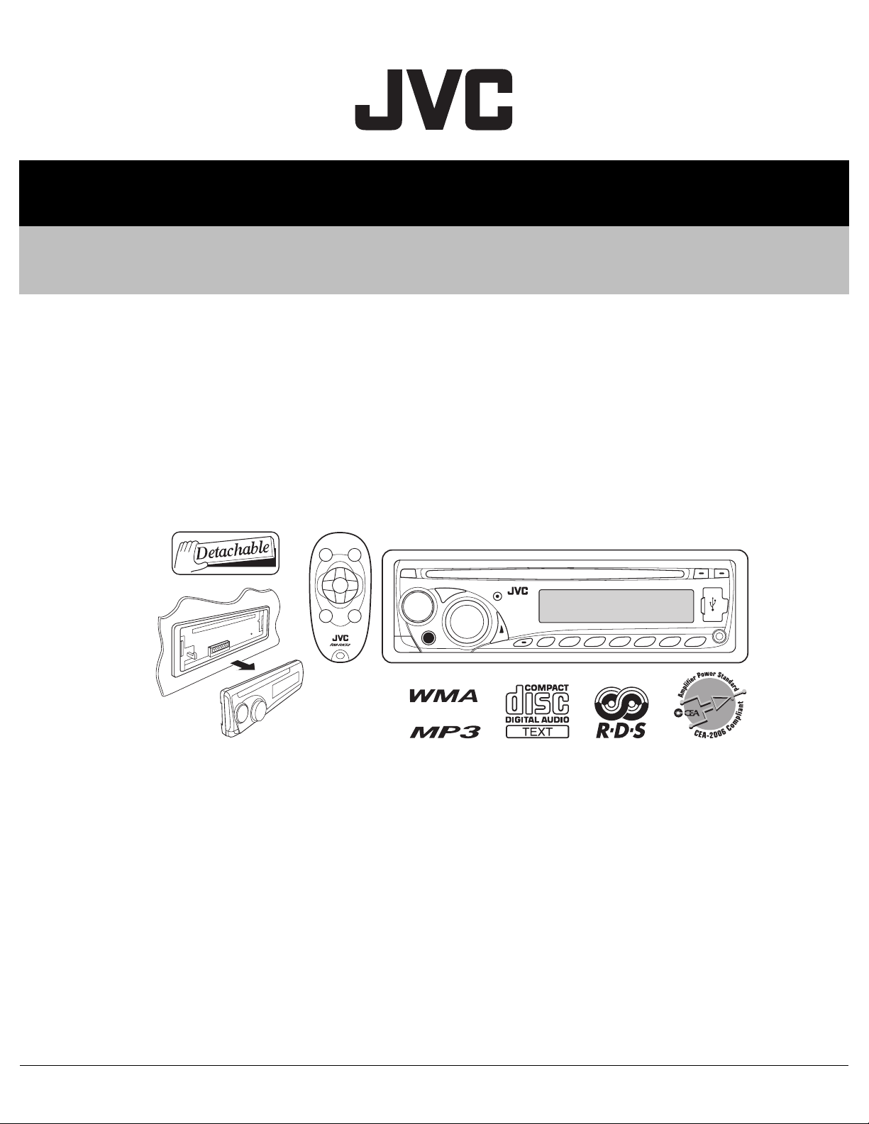
SERVICE MANUAL
CD RECEIVER
MA377<Rev.001>200712SERVICE MANUAL
KD-G351E, KD-G351EX, KD-G351EY, KD-G351EU,
KD-G357EE, KD-G440J, KD-G441E, KD-G441EX,
KD-G441EY, KD-G441EU, KD-G447EE, KD-G644UI,
KD-G645U, KD-G645UN, KD-G645UT, KD-G645UH,
KD-G646U, KD-G646UN, KD-G646UT, KD-G646UH,
KD-G648UF
except
KD-G441
KD-G351
KD-G447
KD-G357
COPYRIGHT © 2007 Victor Company of Japan, Limited
Lead free solder used in the board (material : Sn-Ag-Cu, melting point : 219 Centigrade)
Lead free solder used in the board (material : Sn-Cu, melting point : 230 Centigrade)
only
KD-G441
KD-G351
KD-G447
KD-G357
KD-G440
TABLE OF CONTENTS
1 PRECAUTION. . . . . . . . . . . . . . . . . . . . . . . . . . . . . . . . . . . . . . . . . . . . . . . . . . . . . . . . . . . . . . . . . . . . . . . . . 1-8
2 SPECIFIC SERVICE INSTRUCTIONS . . . . . . . . . . . . . . . . . . . . . . . . . . . . . . . . . . . . . . . . . . . . . . . . . . . . . 1-11
3 DISASSEMBLY . . . . . . . . . . . . . . . . . . . . . . . . . . . . . . . . . . . . . . . . . . . . . . . . . . . . . . . . . . . . . . . . . . . . . . 1-11
4 ADJUSTMENT . . . . . . . . . . . . . . . . . . . . . . . . . . . . . . . . . . . . . . . . . . . . . . . . . . . . . . . . . . . . . . . . . . . . . . . 1-27
5 TROUBLESHOOTING . . . . . . . . . . . . . . . . . . . . . . . . . . . . . . . . . . . . . . . . . . . . . . . . . . . . . . . . . . . . . . . . . 1-28
COPYRIGHT © 2007 Victor Company of Japan, Limited
No.MA377<Rev.001>
only
2007/12
Page 2

SPECIFICATION
KD-G441/KD-G351
AUDIO AMPLIFIER SECTION
Maximum Power Output Front/Rear 50 W per channel
Continuous Power Output (RMS) Front/Rear 19 W per channel into 4 Ω 40 Hz to 20 000 Hz at no
more than 0.8% total harmonic distortion
Load Impedance 4 Ω (4 Ω to 8 Ω allowance)
Tone Control Range Bass ±12 dB at 60 Hz
Middle ±12 dB at 1 kHz
Treble ±12 dB at 10 kHz
Frequency Response 40 Hz to 20 000 Hz
Signal to Noise Ratio 70 dB
Audio Output Level (for KD-G441) Line-Out Level/Impedance 2.5 V/20 kΩ load (full scale)
Output Impedance 1 kΩ
Subwoofer-Out Level/Impedance 2.5 V /20 kΩ load (full scale)
Other Terminals AUX (auxiliary) input jack USB input jack Steering wheel remote input (forKD-G441)
TUNER SECTION
Frequency Range FM 87.5 MHz to 108.0 MHz
AM MW: 522 kHz to 1 620 kHz
LW: 144 kHz to 279 kHz
FM Tuner Usable Sensitivity 11.3 dBf (1.0 µV/75 Ω)
50 dB Quieting Sensitivity 16.3 dBf (1.8 µV/75 Ω)
Alternate Channel Selectivity (400 kHz)
Frequency Response 40 Hz to 15 000 Hz
Stereo Separation 30 dB
MW Tuner Sensitivity/Selectivity 20 µV/35 dB
LW Tuner Sensitivity 50 µV
CD PLAYER SECTION
Type Compact disc player
Signal Detection System Non-contact optical pickup (semiconductor laser)
Number of Channels 2 channels (stereo)
Frequency Response 5 Hz to 20 000 Hz
Dynamic Range 96 dB
Signal-to-Noise Ratio 98 dB
Wow and Flutter Less than measurable limit
MP3 Decoding Format: (MPEG1/2 Audio Layer 3)
WMA (Windows Media® Audio) Decoding Format
USB Standard USB 1.1, USB 2.0
Data Transfer Rate (Full Speed) Max. 12 Mbps
Storage Less than 8 GB (1 partition type)
Compatible Device Mass storage class (except HDD)
Compatible File System FAT 32/16/12
Playable Audio Format MP3/WMA
Max. Current 500 mA
Power Requirement Operating Voltage DC 14.4 V (11 V to 16 V allowance)
Grounding System Negative ground
Allowable Operating Temperature 0°C to +40°C
Dimensions (W × H × D) Installation Size (approx.) 182 mm × 52 mm × 160 mm
Mass (approx.) 1.3 kg (excluding accessories)
Design and specifications are subject to change without notice.
Max. Bit Rate 320 kbps
Max. Bit Rate 320 kbps
USB SECTION
GENERAL
Panel Size (approx.) 188 mm × 58 mm × 13 mm
65 dB
1-2 (No.MA377<Rev.001>)
Page 3
KD-G447/KD-G357
AUDIO AMPLIFIER SECTION
Maximum Power Output Front/Rear 50 W per channel
Continuous Power Output (RMS) Front/Rear 19 W per channel into 4 Ω 40 Hz to 20 000 Hz at no
more than 0.8% total harmonic distortion
Load Impedance 4 Ω (4 Ω to 8 Ω allowance)
Tone Control Range Bass ±12 dB at 60 Hz
Middle ±12 dB at 1 kHz
Treble ±12 dB at 10 kHz
Frequency Response 40 Hz to 20 000 Hz
Signal to Noise Ratio 70 dB
Other Terminals AUX (auxiliary) input jack, USB input jack
TUNER SECTION
Frequency Range FM1/FM2 87.5 MHz to 108.0 MHz
FM3 65.00 MHz to 74.00 MHZ
AM MW: 522 kHz to 1 620 kHz
LW: 144 kHz to 279 kHz
FM Tuner Usable Sensitivity 11.3 dBf (1.0 µV/75 Ω)
50 dB Quieting Sensitivity 16.3 dBf (1.8 µV/75 Ω)
Alternate Channel Selectivity (400 kHz)
Frequency Response 40 Hz to 15 000 Hz
Stereo Separation 30 dB
MW Tuner Sensitivity/Selectivity 20 µV/35 dB
LW Tuner Sensitivity 50 µV
CD PLAYER SECTION
Type Compact disc player
Signal Detection System Non-contact optical pickup (semiconductor laser)
Number of Channels 2 channels (stereo)
Frequency Response 5 Hz to 20 000 Hz
Dynamic Range 96 dB
Signal-to-Noise Ratio 98 dB
Wow and Flutter Less than measurable limit
MP3 Decoding Format: (MPEG1/2 Audio Layer 3)
WMA (Windows Media® Audio) Decoding Format
USB Standard USB 1.1, USB 2.0
Data Transfer Rate (Full Speed) Max. 12 Mbps
Storage Less than 8 GB (1 partition type)
Compatible Device Mass storage class (except HDD)
Compatible File System FAT 32/16/12
Playable Audio Format MP3/WMA
Max. Current 500 mA
Power Requirement Operating Voltage DC 14.4 V (11 V to 16 V allowance)
Grounding System Negative ground
Allowable Operating Temperature 0°C to +40°C
Dimensions (W × H × D) Installation Size (approx.) 182 mm × 52 mm × 160 mm
Mass (approx.) 1.3 kg (excluding accessories)
Design and specifications are subject to change without notice.
Max. Bit Rate 320 kbps
Max. Bit Rate 320 kbps
USB SECTION
GENERAL
Panel Size (approx.) 188 mm × 58 mm × 13 mm
65 dB
(No.MA377<Rev.001>)1-3
Page 4
KD-G440
AUDIO AMPLIFIER SECTION
Power Output 20 W RMS × 4 Channels at 4 Ω and < or = 1% THD+N
Signal-to-Noise Ratio 80 dBA (reference: 1 W into 4 Ω)
Load Impedance 4 Ω (4 Ω to 8 Ω allowance)
Tone Control Range Bass/Mid-range/Treble ±12 dB at 60 Hz/1 kHz/10 kHz
Frequency Response 40 Hz to 20 000 Hz
Line-Out Level/Impedance 2.5 V/20 kΩ load (full scale)
Output Impedance 1 kΩ
Subwoofer-Out Level/Impedance 2.5 V/20 kΩ load (full scale)
Other Terminal AUX (auxiliary) input jack USB input jack Steering wheel remote input
TUNER SECTION
Frequency Range FM
AM
FM Tuner Usable Sensitivity 11.3 dBf (1.0 µV/75 Ω)
50 dB Quieting Sensitivity 16.3 dBf (1.8 µV/75 Ω)
Alternate Channel Selectivity (400 kHz)
Frequency Response 40 Hz to 15 000 Hz
Stereo Separation 35 dB
AM Tuner Sensitivity/Selectivity 20 µV/35 dB
CD PLAYER SECTION
Type Compact disc player
Signal Detection System Non-contact optical pickup (semiconductor laser)
Number of Channels 2 channels (stereo)
Frequency Response 5 Hz to 20 000 Hz
Dynamic Range 96 dB
Signal-to-Noise Ratio 98 dB
Wow and Flutter Less than measurable limit
MP3 Decoding Format: (MPEG1/2 Audio Layer 3)
WMA (Windows Media® Audio) Decoding Format
USB Standard USB 1.1, USB 2.0
Data Transfer Rate (Full Speed) Max. 12 Mbps
Storage Less than 8 GB (1 partition type)
Compatible Device Mass storage class (except HDD)
Compatible File System FAT 32/16/12
Playable Audio Format MP3/WMA
Max. Current 500 mA
Power Requirement Operating Voltage DC 14.4 V (11 V to 16 V allowance)
Grounding System Negative ground
Allowable Operating Temperature 0°C to +40°C (32°F to 104°F)
Dimensions (W × H × D): (approx.) Installation Size
Mass 1.3 kg (2.9 lbs) (excluding accessories)
Design and specifications are subject to change without notice.
Max. Bit Rate 320 kbps
Max. Bit Rate 320 kbps
USB SECTION
GENERAL
Panel Size 188 mm × 58 mm × 6 mm (7-7/16” × 2-5/16” × 1/4”)
87.5 MHz to 107.9 MHz (with channel interval set to 100 kHz or 200 kHz)
87.5 MHz to 108.0 MHz (with channel interval set to 50 kHz)
530 kHz to 1 710 kHz (with channel interval set to 10 kHz)
531 kHz to 1 602 kHz (with channel interval set to 9 kHz)
65 dB
182 mm × 52 mm × 160 mm (7-3/16” × 2-1/16” × 6-5/16”)
1-4 (No.MA377<Rev.001>)
Page 5
KD-G644
AUDIO AMPLIFIER SECTION
Maximum Power Output Front/Rear 50 W per channel
Continuous Power Output (RMS) Front/Rear 19 W per channel into 4 Ω 40 Hz to 20 000 Hz at no
more than 0.8% total harmonic distortion.
Load Impedance 4 Ω (4 Ω to 8 Ω allowance)
Tone Control Range Bass ±12 dB at 60 Hz
Mid-range ±12 dB at 1 kHz
Treble ±12 dB at 10 kHz
Frequency Response 40 Hz to 20 000 Hz
Signal-to-Noise Ratio 70 dB
Line-Out Level/Impedance 2.5 V/20 kΩ load (full scale)
Output Impedance 1 kΩ
Subwoofer-Out Level/Impedance 2.5 V/20 kΩ load (full scale)
Other Terminal AUX (auxiliary) input jack, USB input jack
TUNER SECTION
Frequency Range FM 87.5 MHz to 108.0 MHz
AM 531 kHz to 1 602 kHz
FM Tuner Usable Sensitivity 11.3 dBf (1.0 µV/75 Ω)
50 dB Quieting Sensitivity 16.3 dBf (1.8 µV/75 Ω)
Alternate Channel Selectivity (400 kHz)
Frequency Response 40 Hz to 15 000 Hz
Stereo Separation 30 dB
AM Tuner Sensitivity/Selectivity 20 µV/35 dB
CD PLAYER SECTION
Type Compact disc player
Signal Detection System Non-contact optical pickup (semiconductor laser)
Number of Channels 2 channels (stereo)
Frequency Response 5 Hz to 20 000 Hz
Dynamic Range 96 dB
Signal-to-Noise Ratio 98 dB
Wow and Flutter Less than measurable limit
MP3 Decoding Format: (MPEG1/2 Audio Layer 3)
WMA (Windows Media® Audio) Decoding Format
USB Standard USB 1.1, USB 2.0
Data Transfer Rate (Full Speed) Max. 12 Mbps
Storage Less than 8 GB (1 partition type)
Compatible Device Mass storage class (except HDD)
Compatible File System FAT 32/16/12
Playable Audio Format MP3/WMA
Max. Current 500 mA
Power Requirement Operating Voltage DC 14.4 V (11 V to 16 V allowance)
Grounding System Negative ground
Allowable Operating Temperature 0°C to +40°C
Dimensions (W × H × D): (approx.) Installation Size 182 mm × 52 mm × 160 mm
Mass 1.3 kg (excluding accessories)
Design and specifications are subject to change without notice.
Max. Bit Rate 320 kbps
Max. Bit Rate 320 kbps
USB SECTION
GENERAL
Panel Size 188 mm × 58 mm × 6 mm
65 dB
(No.MA377<Rev.001>)1-5
Page 6
KD-G646/KD-G645
AUDIO AMPLIFIER SECTION
Maximum Power Output Front/Rear 50 W per channel
Continuous Power Output (RMS) Front/Rear 19 W per channel into 4 Ω 40 Hz to 20 000 Hz at no
more than 0.8% total harmonic distortion.
Load Impedance 4 Ω (4 Ω to 8 Ω allowance)
Tone Control Range Bass ±12 dB at 60 Hz
Mid-range ±12 dB at 1 kHz
Treble ±12 dB at 10 kHz
Frequency Response 40 Hz to 20 000 Hz
Signal-to-Noise Ratio 70 dB
Line-Out Level/Impedance 2.5 V/20 kΩ load (full scale)
Output Impedance 1 kΩ
Subwoofer-Out Level/Impedance 2.5 V/20 kΩ load (full scale)
Other Terminal AUX (auxiliary) input jack, USB input jack
TUNER SECTION
Frequency Range FM 87.5 MHz to 108.0 MHz
AM 531 kHz to 1 602 kHz
FM Tuner Usable Sensitivity 11.3 dBf (1.0 µV/75 Ω)
50 dB Quieting Sensitivity 16.3 dBf (1.8 µV/75 Ω)
Alternate Channel Selectivity (400 kHz)
Frequency Response 40 Hz to 15 000 Hz
Stereo Separation 30 dB
AM Tuner Sensitivity/Selectivity 20 µV/35 dB
CD PLAYER SECTION
Type Compact disc player
Signal Detection System Non-contact optical pickup (semiconductor laser)
Number of Channels 2 channels (stereo)
Frequency Response 5 Hz to 20 000 Hz
Dynamic Range 96 dB
Signal-to-Noise Ratio 98 dB
Wow and Flutter Less than measurable limit
MP3 Decoding Format (MPEG1/2 Audio Layer 3)
WMA (Windows Media® Audio) Decoding Format
USB Standard USB 1.1, USB 2.0
Data Transfer Rate Full Speed) Max. 12 Mbps
Storage Less than 8 GB (1 partition type)
Compatible Device Mass storage class (except HDD)
Compatible File System FAT 32/16/12
Playable Audio Format MP3/WMA
Max. Current 500 mA
Power Requirement Operating Voltage DC 14.4 V (11 V to 16 V allowance)
Grounding System Negative ground
Allowable Operating Temperature 0°C to +40°C
Dimensions (W × H × D) (approx.) Installation Size 182 mm × 52 mm × 160 mm
Mass 1.3 kg (excluding accessories)
Design and specifications are subject to change without notice.
Max. Bit Rate 320 kbps
Max. Bit Rate 320 kbps
USB SECTION
GENERAL
Panel Size 188 mm × 58 mm × 6 mm
65 dB
1-6 (No.MA377<Rev.001>)
Page 7

KD-G648
AUDIO AMPLIFIER SECTION
Maximum Power Output Front/Rear 50 W per channel
Continuous Power Output (RMS) Front/Rear 19 W per channel into 4 Ω 40 Hz to 20 000 Hz at no
more than 0.8% total harmonic distortion.
Load Impedance 4 Ω (4 Ω to 8 Ω allowance)
Tone Control Range Bass ±12 dB at 60 Hz
Mid-range ±12 dB at 1 kHz
Treble ±12 dB at 10 kHz
Frequency Response 40 Hz to 20 000 Hz
Signal-to-Noise Ratio 70 dB
Line-Out Level/Impedance 2.5 V/20 kΩ load (full scale)
Output Impedance 1 kΩ
Subwoofer-Out Level/Impedance 2.5 V/20 kΩ load (full scale)
Other Terminal AUX (auxiliary) input jack, USB input jack
TUNER SECTION
Frequency Range FM 87.5 MHz to 108.0 MHz
AM 531 kHz to 1 602 kHz
FM Tuner Usable Sensitivity 11.3 dBf (1.0 µV/75 Ω)
50 dB Quieting Sensitivity 16.3 dBf (1.8 µV/75 Ω)
Alternate Channel Selectivity (400 kHz)
Frequency Response 40 Hz to 15 000 Hz
Stereo Separation 30 dB
AM Tuner Sensitivity/Selectivity 20 µV/35 dB
CD PLAYER SECTION
Type Compact disc player
Signal Detection System Non-contact optical pickup (semiconductor laser)
Number of Channels 2 channels (stereo)
Frequency Response 5 Hz to 20 000 Hz
Dynamic Range 96 dB
Signal-to-Noise Ratio 98 dB
Wow and Flutter Less than measurable limit
MP3 Decoding Format (MPEG1/2 Audio Layer 3)
WMA (Windows Media® Audio) Decoding Format
USB Standard USB 1.1, USB 2.0
Data Transfer Rate Full Speed) Max. 12 Mbps
Storage Less than 8 GB (1 partition type)
Compatible Device Mass storage class (except HDD)
Compatible File System FAT 32/16/12
Playable Audio Format MP3/WMA
Max. Current 500 mA
Power Requirement Operating Voltage DC 14.4 V (11 V to 16 V allowance)
Grounding System Negative ground
Allowable Operating Temperature 0°C to +40°C
Dimensions (W × H × D) (approx.) Installation Size 182 mm × 52 mm × 160 mm
Mass 1.3 kg (excluding accessories)
Design and specifications are subject to change without notice.
Max. Bit Rate 320 kbps
Max. Bit Rate 320 kbps
USB SECTION
GENERAL
Panel Size 188 mm × 58 mm × 6 mm
65 dB
(No.MA377<Rev.001>)1-7
Page 8
1.1 Safety Precautions
SECTION 1
PRECAUTION
!
!
Burrs formed during molding may be left over on some parts of the chassis. Therefore,
pay attention to such burrs in the case of preforming repair of this system.
Please use enough caution not to see the beam directly or touch it in case of an
adjustment or operation check.
1-8 (No.MA377<Rev.001>)
Page 9
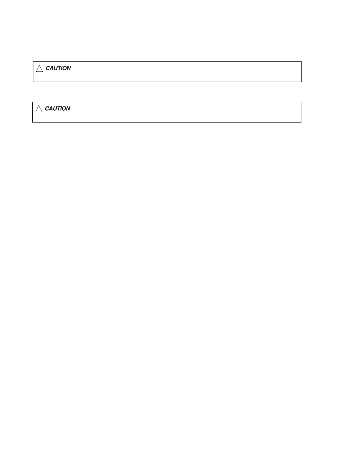
1.2 Preventing static electricity
Electrostatic discharge (ESD), which occurs when static electricity stored in the body, fabric, etc. is discharged, can destroy the laser
diode in the traverse unit (optical pickup). Take care to prevent this when performing repairs.
1.2.1 Grounding to prevent damage by static electricity
Static electricity in the work area can destroy the optical pickup (laser diode) in devices such as laser products.
Be careful to use proper grounding in the area where repairs are being performed.
(1) Ground the workbench
Ground the workbench by laying conductive material (such as a conductive sheet) or an iron plate over it before placing the
traverse unit (optical pickup) on it.
(2) Ground yourself
Use an anti-static wrist strap to release any static electricity built up in your body.
(caption)
Anti-static wrist strap
1M
Conductive material
(conductive sheet) or iron plate
(3) Handling the optical pickup
• In order to maintain quality during transport and before installation, both sides of the laser diode on the replacement optical
pickup are shorted. After replacement, return the shorted parts to their original condition.
(Refer to the text.)
• Do not use a tester to check the condition of the laser diode in the optical pickup. The tester's internal power source can easily
destroy the laser diode.
1.3 Handling the traverse unit (optical pickup)
(1) Do not subject the traverse unit (optical pickup) to strong shocks, as it is a sensitive, complex unit.
(2) Cut off the shorted part of the flexible cable using nippers, etc. after replacing the optical pickup. For specific details, refer to the
replacement procedure in the text. Remove the anti-static pin when replacing the traverse unit. Be careful not to take too long a
time when attaching it to the connector.
(3) Handle the flexible cable carefully as it may break when subjected to strong force.
(4) It is not possible to adjust the semi-fixed resistor that adjusts the laser power. Do not turn it.
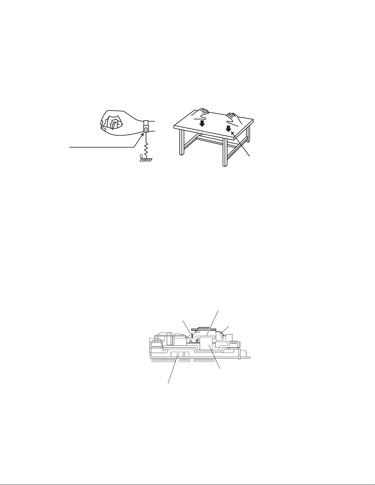
1.4 Attention when traverse unit is decomposed
*Please refer to "Disassembly method" in the text for the pickup unit.
• Apply solder to the short land before the card wire is disconnected from the connector on the pickup unit.
(If the card wire is disconnected without applying solder, the pickup may be destroyed by static electricity.)
• In the assembly, be sure to remove solder from the short land after connecting the card wire.
Connector
Short land section
Pickup
Card wire
Traverse mechanism assembly
(No.MA377<Rev.001>)1-9
Page 10
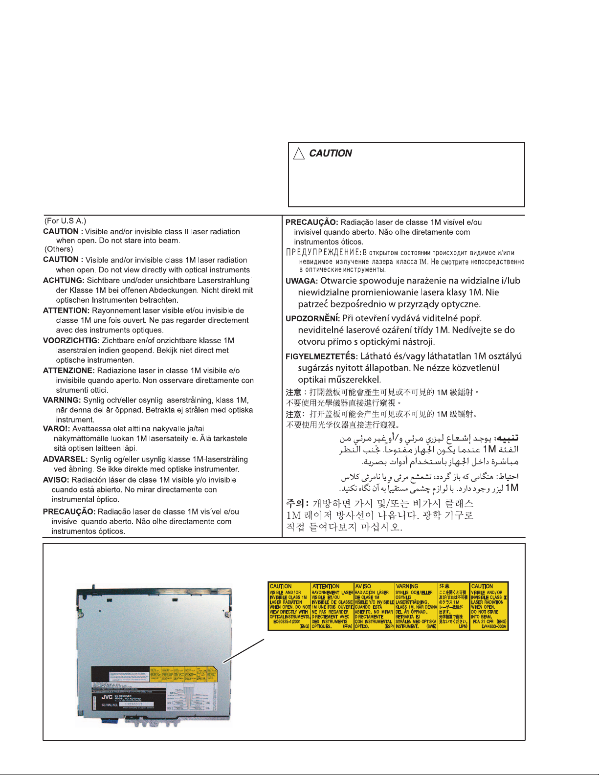
1.5 Important for laser products
1.CLASS 1 LASER PRODUCT
2.CAUTION :
(For U.S.A.) Visible and/or invisible class II laser radiation
when open. Do not stare into beam.
(Others) Visible and/or invisible class 1M laser radiation
when open. Do not view directly with optical instruments.
3.CAUTION : Visible and/or invisible laser radiation when
open and inter lock failed or defeated. Avoid direct
exposure to beam.
4.CAUTION : This laser product uses visible and/or invisible
laser radiation and is equipped with safety switches which
prevent emission of radiation when the drawer is open and
the safety interlocks have failed or are defeated. It is
dangerous to defeat the safety switches.
5.CAUTION : If safety switches malfunction, the laser is able
to function.
6.CAUTION : Use of controls, adjustments or performance of
procedures other than those specified here in may result in
hazardous radiation exposure.
!
Please use enough caution not to
see the beam directly or touch it
in case of an adjustment or operation
check.
REPRODUCTION AND POSITION OF LABELS and PRINT
WARNING LABEL and PRINT
1-10 (No.MA377<Rev.001>)
Page 11
SECTION 2
SPECIFIC SERVICE INSTRUCTIONS
This service manual does not describe SPECIFIC SERVICE INSTRUCTIONS.
SECTION 3
DISASSEMBLY
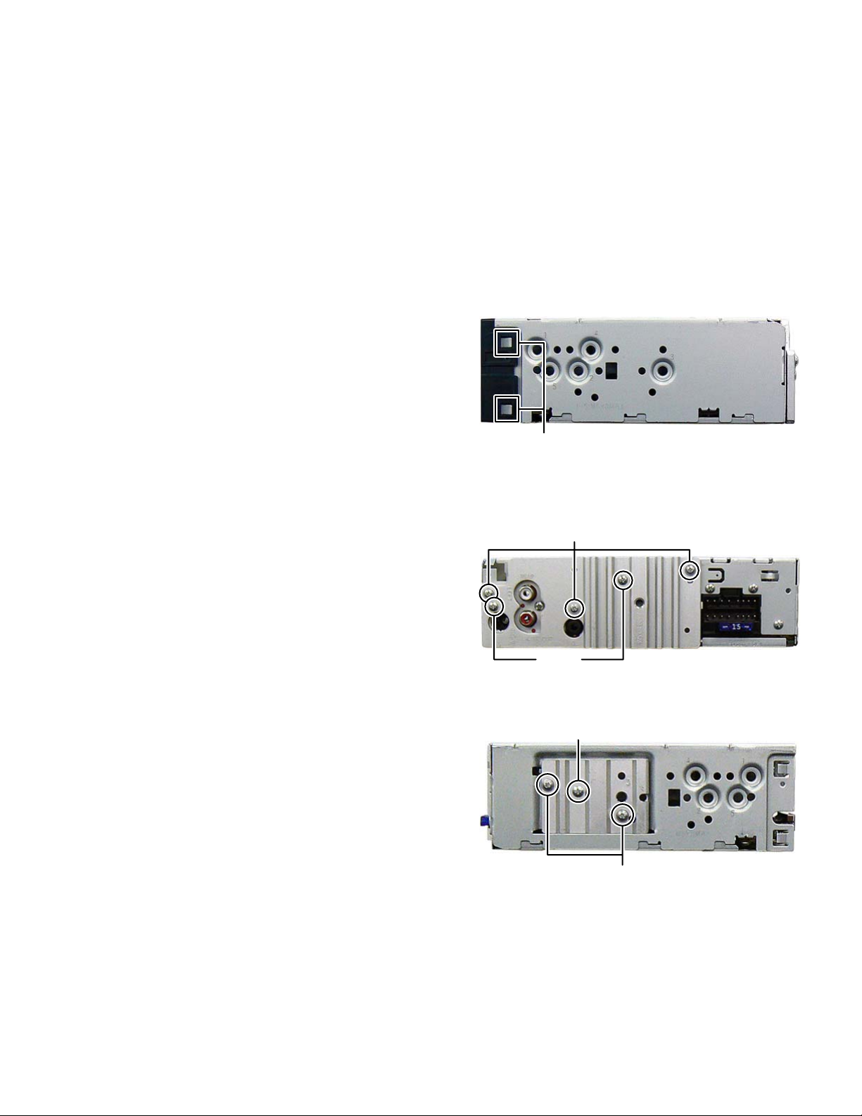
3.1 Main body (used figure is KD-G440)
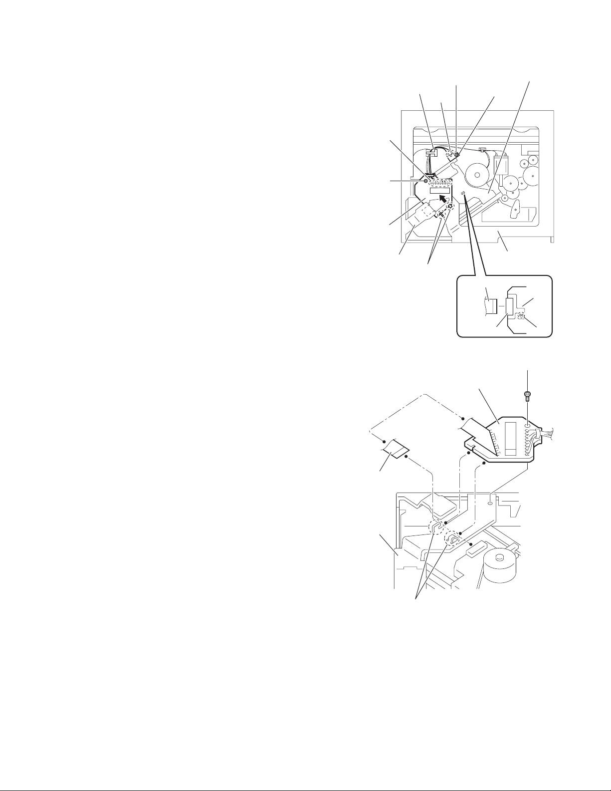
3.1.1 Removing the FRONT CHASSIS assembly (See Fig.3-1)
(1) Disengage the four hooks a engaged the both side of the
FRONT CHASSIS assembly.
hook
a
Fig.3-1
3.1.2 Removing the HEAT SINK (See Fig.3-2, 3-3)
(1) Remove the three screws A and the two screws B attaching
the HEAT SINK. (See Fig.3-2)
(2) Remove the two screws C and the one screw D attaching
the HEAT SINK. (See Fig.3-3)
A
B
Fig.3-2
D
C
Fig.3-3
(No.MA377<Rev.001>)1-11
Page 12
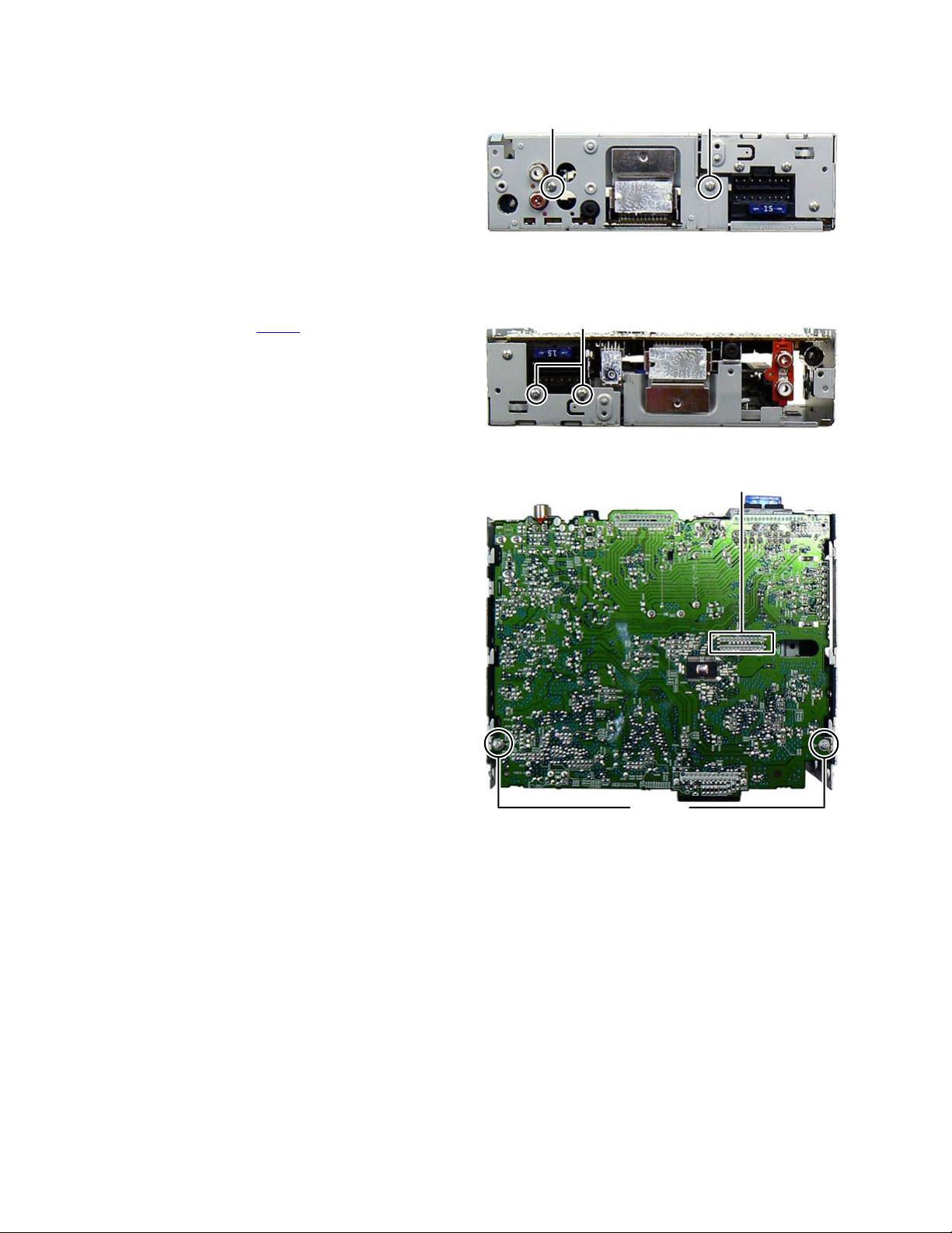
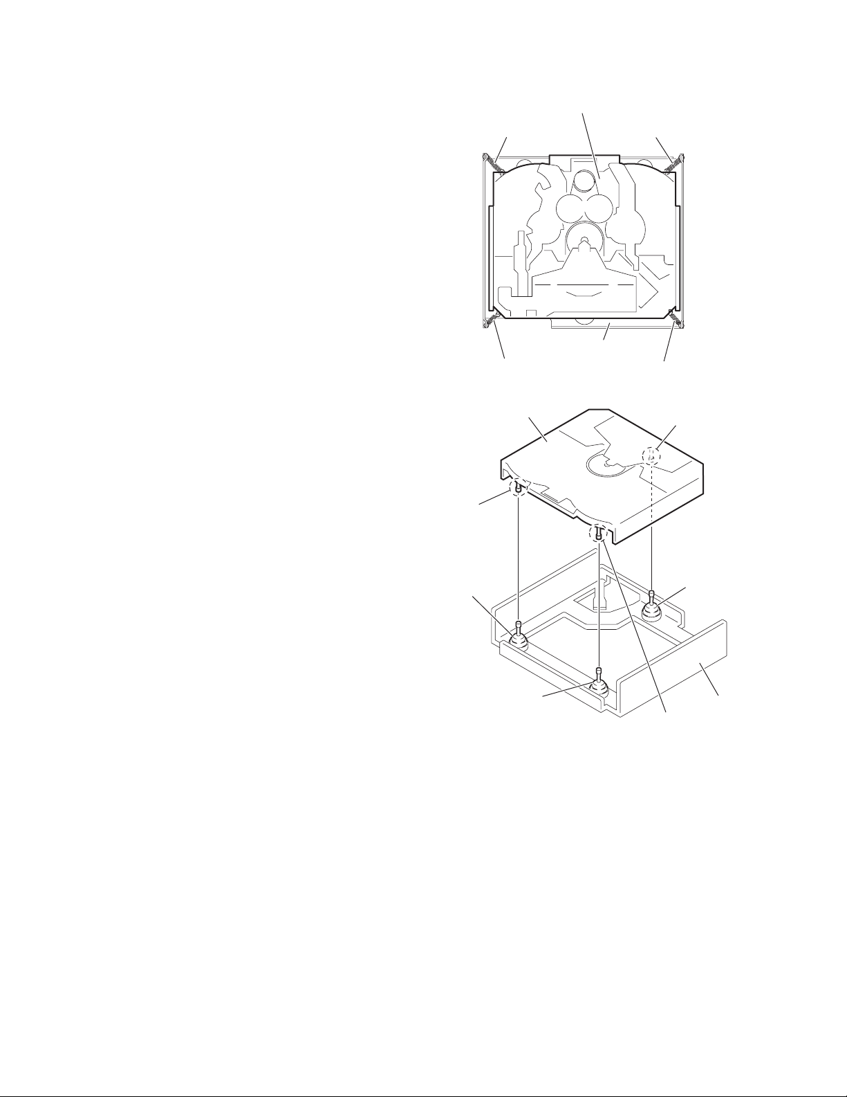
3.1.3 Removing the BOTTOM COVER (See Fig.3-4)
(1) Remove the one screw E and the one screw F attaching
the BOTTOM COVER.
(2) Slide the BOTTOM COVER to backward.
3.1.4 Removing the MAIN BOARD assembly (See Fig.3-5, 3-6)
(1) Remove the two screws G and the two screws H attaching
the MAIN BOARD assembly. (See Fig.3-5, 3-6)
(2) Disconnect the connector CN501
BOARD assembly and CD MECHANISM assembly. (See
Fig.3-6)
connected to MAIN
E F
Fig.3-4
G
Fig.3-5
CN501
1-12 (No.MA377<Rev.001>)
H
Fig.3-6
Page 13
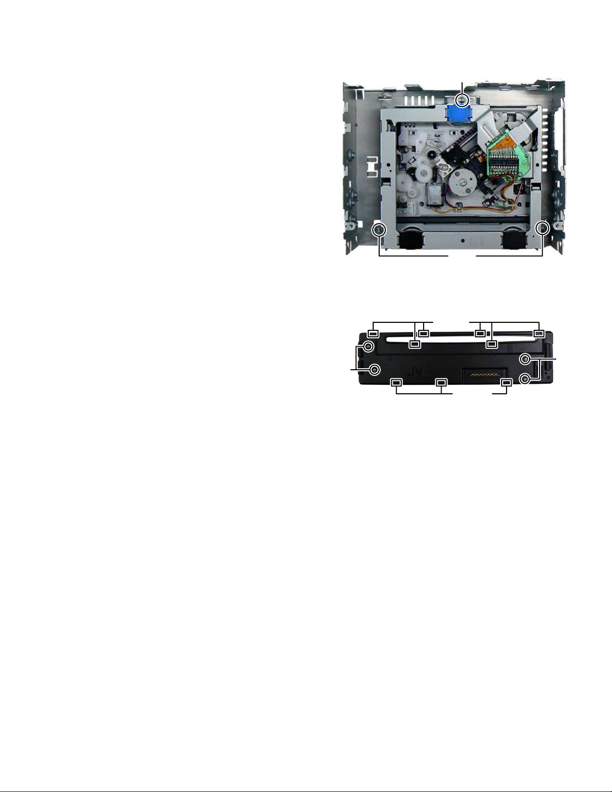
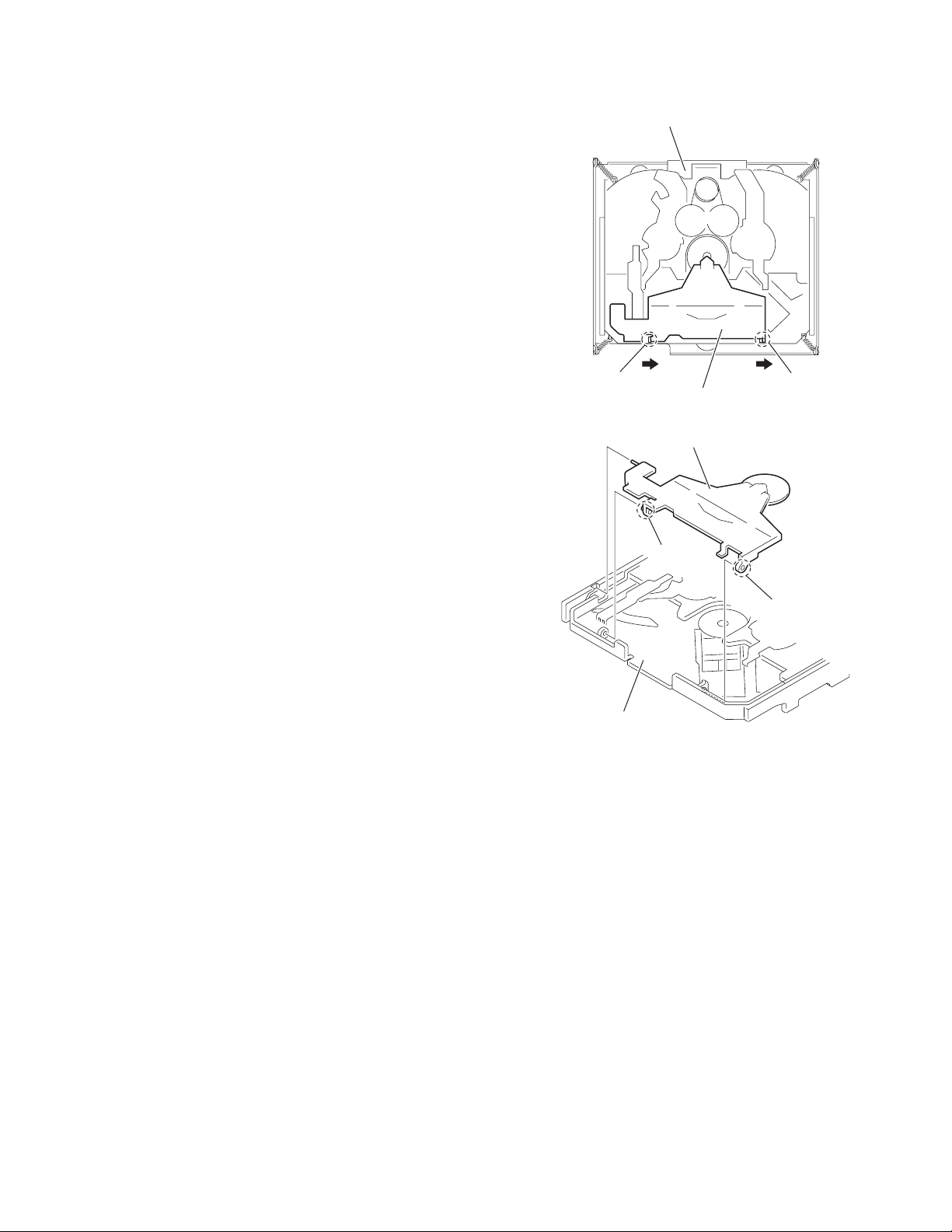
3.1.5 Removing the CD MECHANISM assembly (See Fig.3-7)
(1) Remove the three screws J attaching the CD MECHANISM
assembly.
3.1.6 Removing the SWITCH BOARD assembly (See Fig.3-8)
(1) Remove the VOLUME KNOB.
(2) Remove the four screws K attaching the REAR COVER.
(3) Disengage the nine hooks b engaged the REAR COVER.
J
J
Fig.3-7
hook b
K
K
hook b
Fig.3-8
(No.MA377<Rev.001>)1-13
Page 14
3.2 CD mechanism assembly
A
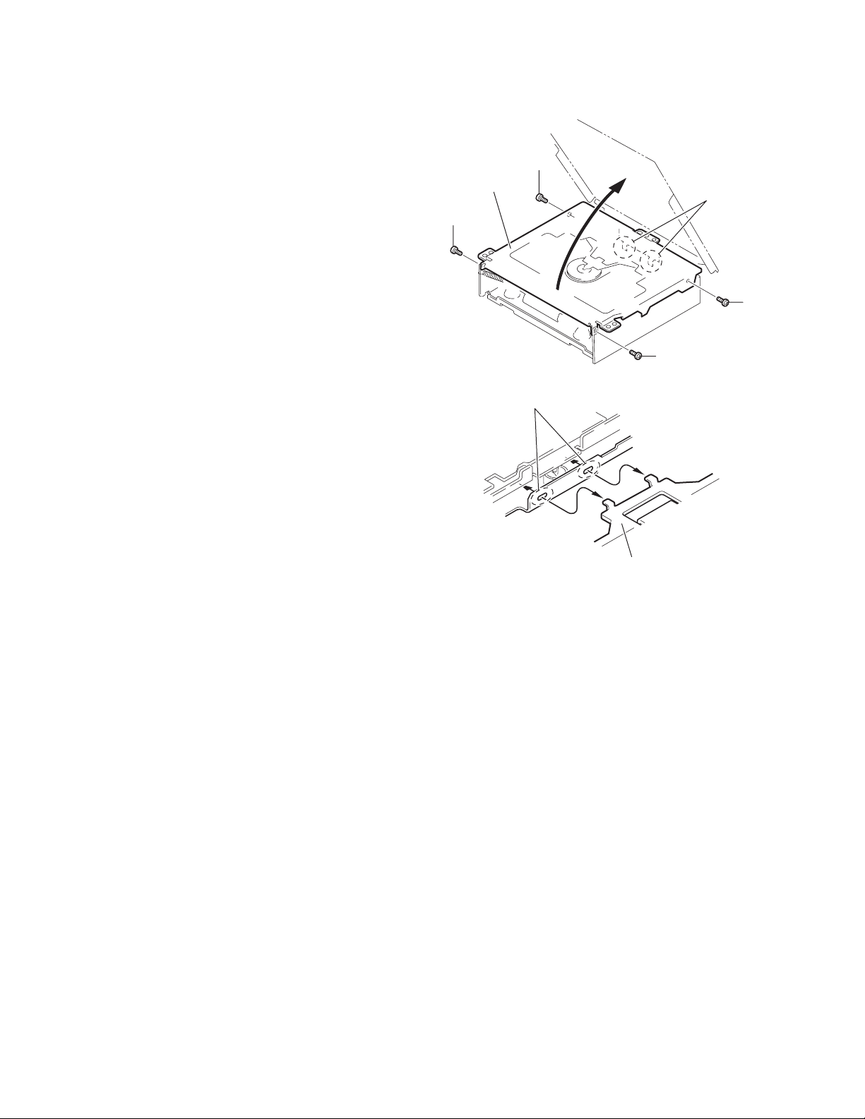
3.2.1 Removing the top cover
(See Figs.1 and 2)
(1) From the both side of the CD mechanism assembly, remove
the four screws A attaching the top cover. (See Fig.1.)
(2) Lift the front side of the top cover and move the top cover
backward to release the two joints a. (See Figs.1 and 2.)
Top cover
A
a
A
A
Fig.1
a
Top cover
Fig.2
1-14 (No.MA377<Rev.001>)
Page 15
3.2.2 Removing the push switch
(See Figs.3)
(1) From the bottom side of the CD mechanism assembly, remove
the screw B attaching the push switch.
(2) Take out the push switch from the CD mechanism assembly.
Reference:
Remove the wires from soldered sections b of the push switch
as required.
3.2.3 Removing the base board
(See Figs.3 and 4)
Caution:
Solder the short land c before the flexible wire is disconnected from
the connector on the pickup. If the flexible wire is disconnected
without applying solder, the pickup may be destroyed by static
electricity. (See Fig.3.)
(1) From the bottom side of the CD mechanism assembly, remove
the screw C attaching the base board. (See Figs.3 and 4.)
(2) Solder the short land c on the pickup. (See Fig.3.)
(3) Disconnect the flexible wire from the connector on the pickup.
(See Fig.3.)
(4) Remove the base board from the joints d of the frame in the
direction of the arrow. (See Figs.3 and 4.)
Reference:
Remove the wires from the soldered sections e on the base
board as required. (See Fig.3.)
Caution:
When reattaching the base board, be sure to remove solder
from the short land c after connecting the flexible wire. (See
Fig.3.)
e
C
Base board
Frame
Wires
B
b
d
Push switch
Flexible wire
Connector
Fig.3
Pickup
CD mechanism
assembly
Pickup
c
C
Base board
Flexible wire
Frame
d
Fig.4
(No.MA377<Rev.001>)1-15
Page 16
3.2.4 Removing the chassis unit
(See Figs.5 and 6)
• Remove the top cover and base board.
(1) From the top side of the CD mechanism assembly, remove
the front suspension springs and rear suspension springs
attaching the chassis unit to the frame. (See Fig.5.)
(2) Remove the chassis unit from the dampers on the frame in
an upward direction. (See Fig.6.)
Note:
• Pay attention to misuse and loss of each spring. (See Fig.5.)
• When reassembling, make sure that the three shafts on the
underside of the chassis unit are inserted to the dampers
certainly. (See Fig.6.)
Chassis unit
Front suspension spring
Front suspension spring
Frame
Rear suspension spring Rear suspension spring
Fig.5
Chassis unit
Shaft
Shaft
Damper F
Damper F
Damper R
Frame
Shaft
Fig.6
1-16 (No.MA377<Rev.001>)
Page 17
3.2.5 Removing the clamper assembly
(See Figs.7 and 8)
• Remove the top cover.
Move the clamper assembly in the direction of the arrow to release
the joints f from the chassis unit.
Chassis unit
f
Clamper assembly
Clamper assembly
Chassis unit
f
Fig.7
f
f
Fig.8
(No.MA377<Rev.001>)1-17
Page 18
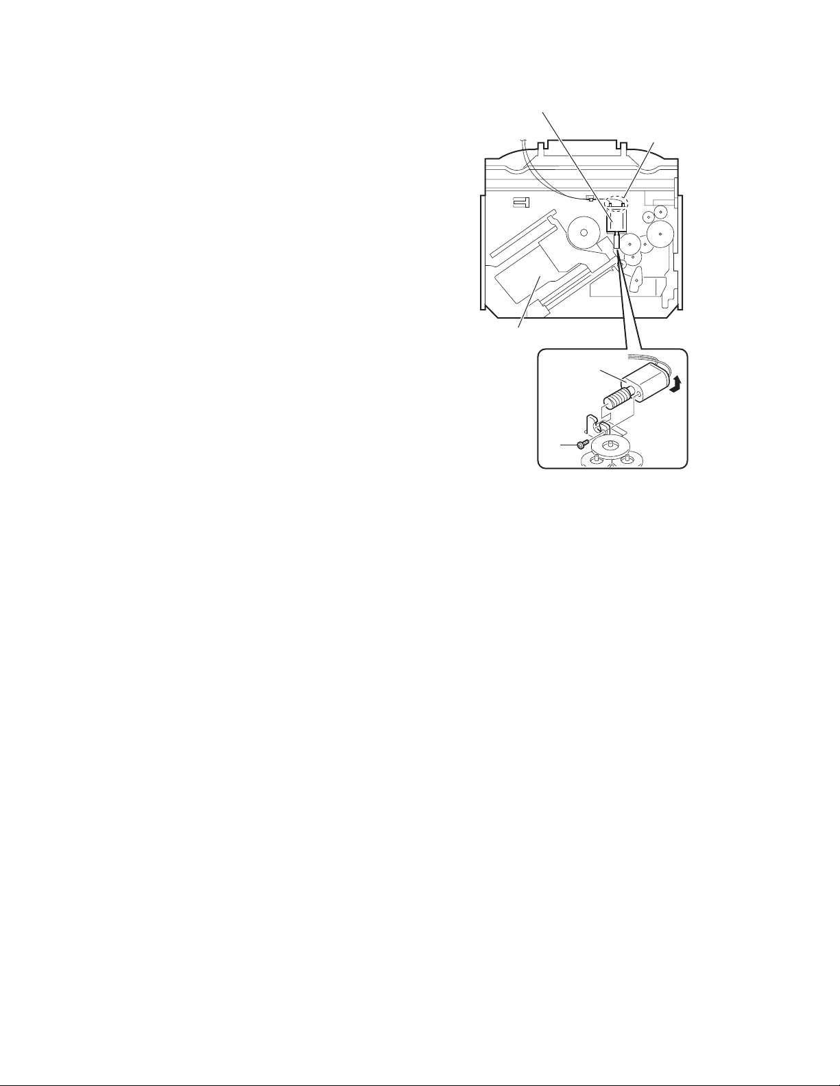
3.2.6 Removing the loading/feed motor assembly
(See Fig.9)
• Remove the top cover, base board and chassis unit.
From the bottom side of the chassis unit, remove the screw D
and take out the loading/feed motor assembly in the direction of
the arrow.
Reference:
Remove the wires from the soldered sections g of the loading/
feed motor assembly as required.
Loading/feed motor assembly
g
Chassis unit
Loading/feed
motor
assembly
D
Fig.9
1-18 (No.MA377<Rev.001>)
Page 19

3.2.7 Removing the pickup
(See Figs.10 to 12)
• Remove the top cover, base board and chassis unit.
(1) From the bottom side of the chassis unit, remove the screw
E attaching the pu. shaft holder B and pull the pu. shaft out
of the pu. shaft holder A. (See Fig.10.)
(2) Remove the screw F attaching the pu. shaft holder A. (See
Fig.10.)
(3) Take out the pickup with pu. shaft holder A and feed screw
assembly from the chassis unit. (See Fig.11.)
(4) Remove the section h of the pu. shaft holder A in the direction
of the arrow. (See Fig.11.)
(5) Remove the feed screw assembly from the section j of the
pickup in the direction of the arrow. (See Fig.11.)
(6) Remove the screw G attaching the feed screw holder to the
pickup. (See Fig.12.)
Reference:
Remove the feed nut spring from the feed screw holder
as required. (See Fig.12.)
(7) Release the claw k in the direction of the arrow to remove
the feed sub holder. (See Fig.12.)
Pickup
Feed screw assembly
Feed screw holder
Pu. shaft holder A
Fig.11
G
h
j
Feed screw
holder
3.2.8 Reattaching the pickup
(See Figs.10 to 13)
(1) Reattach the feed sub holder to the pickup. (See Fig.12.)
(2) Reattach the feed screw holder to the pickup using the
screw G. (See Fig.12.)
(3) Reattach the feed screw assembly and pu. shaft holder A
to the pickup as before. (See Fig.11.)
(4) Set the section m of the pickup to the rail of the chassis unit
at first and attach the pickup to the chassis unit with the
screw F as before. (See Figs.10 and 13.)
(5) Attach the pu. shaft to the pickup as before. (See Fig.10.)
(6) Attach the pu. shaft holder B to the chassis unit with the
screw E as before. (See Fig.10.)
Chassis unit
Pu. shaft holder A
Pu. shaft
F
Pickup
k
Feed sub holder
Pickup
Rail
Feed nut
spring
Fig.12
m
F
E
Pu. shaft holder B
Fig.10
Pickup
Chassis unit
Fig.13
(No.MA377<Rev.001>)1-19
Page 20

3.2.9 Removing the trigger arm
(See Fig.14)
• Remove the top cover, base board, chassis unit and clamper
assembly.
(1) From the top side of the chassis unit, remove the trigger
arm spring from the sections (n, p).
(2) From the bottom side of the chassis unit, release the claws q
of the trigger arm base in the direction of the arrow to remove
them from the sections r of the chassis unit to the other side.
Note:
When releasing the claws q, take care not to break them.
(3) From the top side of the chassis unit, move the select arm R
and select lock arm in the direction of the arrow to remove
the trigger arm base from the section s in the direction of the
arrow.
(4) Remove the trigger arm from the section t.
3.2.10 Removing the top plate assembly
(See Fig.15)
• Remove the top cover, base board, chassis unit, clamper assembly
and trigger arm.
(1) Remove the screw H attaching the top plate assembly.
(2) Move the top plate assembly in the direction of the arrow to
release the joints (u, v).
Reference:
Remove the wires from the soldered sections w of the top plate
assembly as required.
Note:
When reassembling, solder the wires as before.
Select lock arm
Trigger arm
spring
u
v
Select arm R
s
n
t
p
Chassis unit
Top plate assembly
Chassis unit
Trigger arm base
Trigger arm
q
r
Fig.14
H
w
Wire(Red)
1-20 (No.MA377<Rev.001>)
Wire(White)
Wire(Brown)
Fig.15
Page 21

3.2.11 Removing the mode switch
(See Fig.16)
• Remove the top cover, base board, chassis unit, clamper assembly,
trigger arm and top plate assembly.
(1) From the top side of the top plate assembly, remove the
link gear spring from the sections x of the link gear L and
link gear R.
(2) Remove the link gear L in an upward direction while releasing
the claws y of the link gear L in the direction of the arrow.
(3) Move the mode switch in the direction of the arrow 1 to remove
the sections z of the top plate assembly.
(4) Move the mode switch in the direction of the arrow 2 and
remove the mode switch from the sections (aa, ab).
Note:
When reattaching the link gear L, attach it after aligning the
hole ac of the link gear L to the hole ac of the link gear R.
Reference:
When reassembling, reverse the above removing procedure.
Top plate assembly
Link gear spring
Link gear R
Link
gear R
Link
gear L
ac ac
aa
Link gear L
Fig.16
Mode switch
x
1
2
z
y
y
ab
(No.MA377<Rev.001>)1-21
Page 22

3.2.12 Removing the select arm R and select lock arm
(See Figs.17 and 18)
• Remove the top cover, base board, chassis unit, clamper assembly,
trigger arm and top plate assembly.
(1) From the top side of the top plate assembly, remove the
link gear spring from the sections ad of the link gear L and
link gear R. (See Fig.17.)
(2) Remove the link gear R in an upward direction while releasing
the claws ae of the link gear R in the direction of the arrow.
(See Fig.17.)
(3) Move the select arm R in the direction of the arrow 1 to remove
the sections af of the top plate assembly. (See Fig.17.)
(4) Move the select arm R in the direction of the arrow 2 and
remove the select arm R from the sections ag. (See
Fig.17.)
(5) From the bottom side of the top plate assembly, remove
the select lock arm spring from the section ah. (See
Fig.18.)
(6) From the top side of the top plate assembly, remove the section
aj of the select lock arm from the top plate assembly at first and
remove the sections (ak, am) of the select lock arm from the top
plate assembly. (See Fig.18.)
Note:
• When removing the select lock arm spring, be careful not to
lose it. (See Fig 18.)
• When reattaching the link gear R, attach it after aligning the
hole an of the link gear R to the hole an of the link gear L.
(See Fig.17.)
Reference:
When reassembling, reverse the above removing procedure.
ak
ae
2
af
ae
Select arm R
ad
1
ag
Link gear R
Select lock arm
aj
Link gear spring
Top plate assembly
Link gear L
Link
gear R
an an
Fig.17
Top plate assembly
Link
gear L
1-22 (No.MA377<Rev.001>)
Select lock
arm spring
ah
am
Fig.18
Page 23

3.2.13 Removing the loading roller assembly
(See Figs.19 to 21)
• Remove the top cover, base board, chassis unit, clamper assembly
and top plate assembly.
(1) From the left side of the chassis unit, remove the screw J
attaching the lock arm assembly. (See Fig.19.)
(2) Remove the projection ap of the lock arm assembly from
the joint aq while opening the cam plate R in the direction
of the arrow. (See Fig.19.)
(3) Remove the lock arm assembly from the projection ar of
the chassis unit. (See Fig.19.)
(4) Remove the projection as of the lock arm assembly from
the joint at of the cam plate L assembly. (See Fig.19.)
(5) From the right side of the lock arm assembly, remove the
loading roller spring L from the section au. (See Fig.20.)
(6) From the top side of the lock arm assembly, remove the loading
roller spring R in the direction of the arrow and remove the loading
roller assembly. (See Fig.20.)
(7) Remove the roller guide R, HL washer and roller guide L
from the both ends of the loading roller assembly. (See
Fig.21.)
aq
J
ap
Lock arm assembly
Loading roller assembly
Cam plate R
Fig.19
Chassis unit
Cam plate L assembly
ar
Loading roller spring R
at
as
Lock arm assembly
Loading roller
spring L
au
Fig.20
Roller guide L Roller guide R
HL washer
Loading roller assembly
Fig.21
(No.MA377<Rev.001>)1-23
Page 24

3.2.14 Removing the loading gear 1, loading gear 2, loading gear 3 and feed gear 1
(See Fig.22)
• Remove the top cover, base board and chassis unit.
(1) From the bottom side of the chassis unit, pull out the loading
gear 1.
(2) Take out the loading gear 2.
(3) Pull out the loading gear 3.
(4) Pull out the feed gear 1.
3.2.15 Removing the loading gear 4, loading gear 5 and
loading gear 6
(See Fig.22)
• Remove the top cover, base board and chassis unit.
(1) From the bottom side of the chassis unit, remove the screw
K attaching the loading gear bracket.
(2) Take out the loading gear bracket and remove the loading
gear 5 and loading gear 6 from the loading gear bracket.
(3) Pull out the loading gear 4.
Loading gear bracket
Loading gear 3
Feed gear 2
Loading gear 6
Loading gear
bracket
Loading gear 4
Loading gear 1
Loading
gear 5
K
3.2.16 Removing the change gear 2, change gear 3A and
change gear 3B
(See Figs.22 and 23)
• Remove the top cover, base board and chassis unit.
(1) From the bottom side of the chassis unit, pull out the loading
gear 1. (See Fig.22.)
(2) Pull out the change gear 2. (See Fig.22.)
(3) Pull out the change arm. (See Fig.22.)
(4) Move the change gear plate rivet assembly in the direction
of the arrow 2 to remove the section av of the change gear
plate rivet assembly from the chassis unit while moving the
change lock lever in the direction of the arrow 1. (See
Fig.23.)
(5) Pull out the change gear 3A and change gear 3B from the
change gear plate rivet assembly. (See Fig.23.)
3.2.17 Removing the cam plate L assembly
(See Fig.24)
• Remove the top cover, base board, chassis unit, clamper assembly,
top plate assembly and loading roller assembly.
(1) From the left side of the chassis unit, slide the cam plate L
assembly in the direction of the arrow.
(2) Remove the cam plate L assembly from the slots aw of the
chassis unit.
Feed gear 1
Chassis unit
Change gear plate rivet assembly
Change gear 3B
1
Chassis unit
Change lock lever
Chassis unit
Change arm
Fig.22
2
Fig.23
Loading gear 2
Change gear plate
rivet assembly
Change
gear 3A
Change gear 3B
Change gear 3A
av
aw
1-24 (No.MA377<Rev.001>)
aw
Cam plate L assembly
Fig.24
Page 25

3.2.18 Removing the cam plate R
(See Fig.25)
• Remove the top cover, base board, chassis unit, clamper assembly,
top plate assembly and loading roller assembly.
From the right side of the chassis unit, remove the cam plate R
from the slots ax of the chassis unit.
Reference:
When a slide hook rivet assembly and a trigger rack spring have
come off from the chassis unit, attach them before attaching the
cam plate R.
3.2.19 Removing the trigger rack plate
(See Figs.25 and 26)
• Remove the top cover, base board, chassis unit, clamper assembly,
top plate assembly, loading roller assembly and cam plate R.
(1) Remove the slide hook rivet assembly and trigger rack
spring from the chassis unit. (See Fig.25.)
(2) From the bottom side of the chassis unit, pull out the loading
gear 1. (See Fig.26.)
(3) Remove the trigger control spring from the sections (ay,
az). (See Fig.26.)
(4) Take out the trigger rack plate from the chassis unit. (See
Fig.26.)
Reference:
When attaching the trigger rack plate, insert the projection a'
of the chassis unit in the slot b' on the bottom side of the trigger
rack plate as before. (See Fig.26.)
Chassis unit
ax
Cam plate R
b'
Trigger rack spring
Slide hook rivet assembly
ax
Fig.25
Trigger control spring
az
a'
Trigger
rack plate
Trigger rack plate
Loading gear 1
ay
Chassis unit
Fig.26
(No.MA377<Rev.001>)1-25
Page 26

3.2.20 Removing the spindle motor assembly
(See Figs.27 and 28)
• Remove the top cover, base board, chassis unit and clamper
assembly.
(1) From the top side of the chassis unit, turn the turn table from
side to side and remove the two screws M attaching the
spindle motor assembly through the hole of the turn table.
(See Fig.27.)
(2) From the bottom side of the chassis unit, turn the change
gear 2 in the direction of the arrow 2 while pulling the trigger
arm in the direction of the arrow 1 and let the pickup move
in the direction of the arrow 3. (See Fig.28.)
(3) Slide the spindle motor assembly in the direction of the arrow
and take out it in an upward direction from the chassis unit.
(See Fig.28.)
Reference:
Remove the wires from the soldered sections c' on the base
board and remove them from the sections (d', e') on the chassis
unit as required.
Chassis unit
Wire(black)
Wire(red)
M
Fig.27
Spindle motor assembly
d'
Turn table
e'
Change gear 2
c'
Base board
3
Pickup
2
1
Trigger arm
Chassis unit
Fig.28
1-26 (No.MA377<Rev.001>)
Page 27

SECTION 4
ADJUSTMENT
4.1 Test instruments required for adjustment
(1) Digital oscilloscope (100MHz)
(2) Electric voltmeter
(3) Digital tester
(4) Tracking offset meter
(5) Test Disc JVC :CTS-1000
(6) Extension cable for check
EXTSH002-22P x 1
4.2 Standard measuring conditions
Power supply voltage DC14.4V(10.5 to 16V)
Load impedance 20K.(2 Speakers connection)
Output Level Line out 2.5V (Vol. MAX)
4.5 How to connect the extension cable for adjusting
Caution:
Be sure to attach the heat sink and rear bracket onto the power amplifier IC and regulator IC respectively, before supply the power.
If voltage is applied without attaching these parts, the power amplifier IC and regulator IC will be destroyed by heat.
4.3 Standard volume position
Balance and Bass &Treble volume : lndication"0"
Loudness : OFF
4.4 Dummy load
Exclusive dummy load should be used for AM,and FM.
For FM dummy load, there is a loss of 6dB between SSG output
and antenna input.
The loss of 6dB need not be considered sincedirect reading of
figures are applied in this working standard.
Extension cable
EXTSH002-22P
(No.MA377<Rev.001>)1-27
Page 28

SECTION 5
TROUBLESHOOTING
5.1 16PIN CORD DIAGRAM (for KD-G351, KD-G357, KD-G441, KD-G447)
8
7
6
5
4
3
2
1
BK
RD
NC
BL/WH
WH
GN
VI
GY
YL
NC
NC
BR
WH/BK
GN/BK
VI/BK
GY/BK
16
15
14
13
12
11
10
9
BK
RD
BL
WH
BR
Black
Red
Blue
White
Brown
GN
VI
GY
YL
Green
Violet
Gray
Yellow
BR
NC
1
NC
3
BL/WH
5
RD
7
YL
NC
BK
2
4
6
8
RR
FR
FL
RL
7 RD
16 YL
8 BK
5 BL/WH
13 BR
3 GN
11 GN/BK
2 VI
10 VI/BK
4 WH
12 WH/BK
1 GY
9 GY/BK
Rear Right
Front Right
Front Left
Rear Left
ACC
TEL
GND
MEMORY
RD
ACC Line
Telephone Muting
Ground
Memory Backup Battery+
RD 7
YL 4
8
5
2
7
8
1
2
5
6
3
4
VI/BK
VI
1
GY
3
WH
5
GN
7
GY/BK
WH/BK
GN/BK
2
4
6
8
REMOTE
ILL
1-28 (No.MA377<Rev.001>)
Remote
Illuminations Control
ANT
Auto Antenna
Page 29

5.2 16 PIN CORD DIAGRAM (for KD-G440)
BK
RD
BL
WH
Black
Red
Blue
White
8
7
6
5
4
3
2
1
BK
8
BK
RD
NC
BL/WH
WH
GN
VI
GY
GN
VI
GY
YL
YL
NC
NC
NC
WH/BK
GN/BK
VI/BK
GY/BK
Green
Violet
Gray
Yellow
16
15
14
13
12
11
10
9
16
5
7
3
11
2
10
4
12
1
YL
BL/WH
RD
GN
GN/BK
VI
VI/BK
WH
WH/BK
GY
9
GY/BK
(No.MA377<Rev.001>)1-29
Page 30

5.3 16 PIN CORD DIAGRAM (for KD-G644, KD-G645, KD-G646)
BK
RD
BL
WH
Black
Red
Blue
White
8
7
6
5
4
3
2
1
BK
RD
BL
BL/WH
WH
GN
VI
GY
GN
VI
GY
YL
OR
YL
OR/WH
NC
NC
WH/BK
GN/BK
VI/BK
GY/BK
Green
Violet
Gray
Yellow
Orange
16
15
14
13
12
11
10
9
8
16
15
3
11
10
4
7
2
12
1
9
5
BK
YL
RD
OR / WH
GN
GN / BK
VI
VI / BK
WH
WH / BK
GY
GY / BK
BL / WH
6
1-30 (No.MA377<Rev.001>)
BL
Page 31

5.4 16 PIN CORD DIAGRAM (for KD-G648)
YL1
OR/WH
NC
NC
WH/BK
GN/BK
VI/BK
GY/BK
16
15
14
13
12
11
10
9
8
7
6
5
4
3
2
1
BK
RD1
BL
BL/WH
WH
GN
VI
GY
BK
RD
BL
WH
BR
Black
Red
Blue
White
Brown
GN
VI
GY
YL
OR
Green
Violet
Gray
Yellow
Orange
1
NC
NC
3
5
BL
7
RD2
NC
YL2
OR/WH
BK
2
4
6
8
7
16
8
6
15
3
11
2
10
4
12
1
9
5
RD1
YL1
BK
BL
OR/WH
GN
GN/BK
VI
VI/BK
WH
WH/BK
GY
GY/BK
BL/WH
RD3
RD2
YL 2
7
4
8
5
6
7
8
1
2
5
6
3
4
VI/BK
GY/BK
WH/BK
GN/BK
2
4
6
8
VI
1
3
GY
5
WH
GN
7
(No.MA377<Rev.001>)1-31
Page 32

Victor Company of Japan, Limited
Mobile Entertainment Business Group Mobile Entertainment Category 10-1,1chome,Ohwatari-machi,Maebashi-city,371-8543,Japan
(No.MA377<Rev.001>)
Printed in Japan
VPT
Page 33

SCHEMATIC DIAGRAMS
CD RECEIVER
KD-G351E,KD-G351EX,KD-G351EY
KD-G351EU,KD-G357EE,KD-G440J
KD-G441E,KD-G441EX,KD-G441EY
KD-G441EU,KD-G447EE,KD-G644UI
KD-G645U,KD-G645UN,KD-G645UT
KD-G645UH,KD-G646U,KD-G646UN
KD-G646UT,KD-G646UH,KD-G648UF
CD-ROM No.SML200712
except
KD-G441
KD-G351
KD-G447
KD-G357
Lead free solder used in the board (material : Sn-Ag-Cu, melting point : 219 Centigrade)
Lead free solder used in the board (material : Sn-Cu, melting point : 230 Centigrade)
Contents
Block diagram
Standard schematic diagrams
Printed circuit boards
2-1
2-2
2-5 to 7
only
KD-G441
KD-G351
KD-G447
KD-G357
KD-G440
only
COPYRIGHT 2007 Victor Company of Japan, Limited.
No.MA377SCH
2007/12
Page 34

Safety precaution
!
!
Burrs formed during molding may be left over on some parts of the chassis. Therefore,
pay attention to such burrs in the case of preforming repair of this system.
Please use enough caution not to see the beam directly or touch it in case of an
adjustment or operation check.
Page 35

Block diagram
CD MECHA
LOAD & FEED
MOTOR
POSITION
SET SWITCH
SPINDLE
MOTOR
SW1,SW2
CD PICK UP
PICK UP
FOCUS & TRACKING
FEED+/-
PSW
SP+/-
SW1
SW2
VF1, VF2
VT1, VT2
MD, LD
COIL
CN001
TRK+/FOCUS+/-
CD servo control section
VF1
VF2
VT1
VT2
MD
LD
X521
16.9344MHz
CN501
SP+/FEED+/FOCUS+/TRK+/-
PSW
SW1, SW2
SRAMVDD
IC521
Q521
RF AMP
IC501,Q501
BTL DRIVER
IC981
1.5V REG.
14.31818MHZ
OUTL/R CD-USB.L/R
IC581
CD L.P.F.
IRQ
NPWDOWN
NRST
STAT
MLD
MDATA
MCLK
FOP
TRP
TRVP
SPOUT
LM
MSW
VDD5V
CD-NRST
CD-STAT
CD-MLD
CD-DATA
CD-MCLK
IC401
USB
X401
DECODER
I2C-DATA
I2C-REQ
I2C-CLK
USB_CON
USB-RST
USB-DET
USBD+/-
Main amplifier & System control section
X701
8MHz
X702
32.768kHz
E2PROM_DI
E2PROM_DO
IC771
EPROM
IC702,S701
RESET
Q976,Q977
PS2
E2PROM_CLK
RST
PS2
IC701
CPU
TUSDA
TUSCL
SUB-MUTE
MUTE
VOL_SDA
VOL_CLK
RDSDA
RDSCL
X1
4MHz
CD-USB.L/R
Used for
KD-G351, KD-G357
KD-G441, KD-G447
IC71
RDS DETECTOR
MPXOUT
IC1
FM/AM TUNER
TU.L/R
CONTROL
IC161
E.VOLUME
SUBL.RL
SUBR.RR
Q781
Q782
MUTE
X71
4.332MHz
Used for
KD-G440, KD-G441
KD-G644, KD-G645, KD-G646, KD-G648
Q331,Q785
REAR/SUBW
REAR/
SUBWOOFER L/R
LINE OUT MUTING
Used for
KD-G644, KD-G645
KD-G646, KD-G648
Q321
FRONT
FRONT L/R
LINE OUT MUTING
MUTE
LFOUT
RFOUT
LROUT
RROUT
IC301
POWER AMP.
FL+/FR+/RL+/RR+/-
J1
ANT
REAR &
SUBWOOFER
LINE OUT
FRONT
LINE OUT
USB
AUX
INPUT
J601J602
LCD , AUX/USB Jack & Key control section
D+/-
USB5V
LCD1
COM1 to 4
S1 to 50
LCD MODULE
IC681
REMOCON
JS686
REMOCON
Used for
KD-G440, KD-G441, KD-G447
KD-G644, KD-G645, KD-G646, KD-G648
VOL1
VOL2
ENCODER
KEY0
KEY1
S601 to S619
KEY2
KEY MATRIX
AUX.L/R
D630
POWER LED
D631 to D654
LIGHTING DISPLAY
ACC5V
ILM.10V
IC661
LCD DRIVER
LCDDA
LCDCE
LCDCL
USB5V MEMORY
IC931,IC941
USB5V REG.
KEY2
LCDDA
LCDCE
LCDCL
REMOCON
CN701
CJ601
VOL1
VOL2
KEY0
KEY1
DIMOUT
ANT
CD_ON
Q882,Q883
DIMMER
CONTROL
ILM.ADJ
AUX.L/R
POWER
3.3V,SW5V,ACC5V
VDD5V,CD8V,9V,ILM.10V
EACH BLOCK
ACC.IN
EXT
IC901
MEMORY
REGULATOR
ANT
D851
AUTO ANTENNA
DIMIN
Q881
DIMMER INPUT
Used for KD-G644, KD-G645, KD-G646, KD-G648
TELMUTE
Q891
TELMUTE
Used for KD-G351, KD-G357, KD-G441, KD-G447
Used for KD-G440,KD-G441
ANT
ILLUMINATION
TELMUTE
STEERING
CN901J321
SPK
BATTERY
CN703
STEERING
REMOTE
2-1
Page 36

Standard schematic diagrams
Main section
0.01
1.5V
AMSELIN2
FMRFIN1
3.3V
2.5V
CIN
TEST
0V
C78
C76
C12
0V
0V
0V
0V
AMSELIN1
GNDRF
GND
GND
330p
0.01
3900p
4.9V
4.9V
1.5V
Vdd
Vdd
PLL2
VCC
8.5V
C25
C73
10/25
2.5V
MUX
OSCI
2.5V
QAX0926-001Z
C75
33p
AUX.R
AUX.G
AUX.L
0.1
C16
0.01
C17
C18
4.7K
2.3V
2.3V
3.2V
R4
IC1
PLLREF
*
AMRFAGC
0V
3.8V
1.8V
1
C13
0.01
RDSDA
NI
2.2k
R75
R73
( )
2.5V
0V
2.4V
12345678
Vref
QUAL
DATA
CLK
T57
OSCO
R72
2.2K
0V
2.5V
2.5V
R71
0
X71
*
CD_8V
CD-USB.R
AGND
CD-USB.L
9V
VDD_5V
USB-RST
USB_CON
I2C-CLK
I2C-DATA
I2C-REQ
USB-DET
SW1
SW2
PSW
NPWDOWN
MSW
LM
NRST
IRQ
STAT
MLD
MDATA
MCLK
DGND
RFGND
3.3V
USB-DUSB-D+
KEY2
SW5V
CN701
QGZ1101J1-24
DETACH CONNECTOR
AUX.R
1
AUX.G
2
AGND
3
AUX.L
4
ACC5V
5
6
USBGND
7
USB-D-
8
USB-D+
9
10
USB5V
11
VOL2
12
VOL1
13
REMOCON
14
DGND
15
10V
16
LCDCL
17
LCDCE
18
LCDDA
19
20
21
KEY0
To LCD & Key control section To CD section
22
KEY1
23
KEY2
24
STEERING REMOTE CONTROL
FOR KD-G441E SERIES AND KD-G440J ONLY
CN703
QNS0283-001
3
2
1
D711
UDZW6.2B-X
J1
QNB0190-001
22p
C419
22p
C418
C710
100P
R1
FM/AM
TUNER
L8
4.7u
*
D1
47/6.3
D719,D720:
UDZW6.2B-X
1SS355W-X
C414
D719
C1
0.001
QQR1773-001
D2
C991
( )
D701
D701-D709:
L3
1SS355W-X
NI
D702
R2
D703
L1
C2
*
D720
0.47u
5.6p
D716
D715-D718:
( )
D704
UDZW6.2B-X
C34
C5
15p
F401
NAD0031-005X
C729
1000p
R725
10k
D715
( )
( )
D706
D705
C32
100p
( )
C33
22P
750mA
UDZW6.2B-X
( )
D707
L6
L5
560u
560u
1
C10
C11
0
R10
*
3.0V
6.8V
0V
1.4V
8.5V
6.8V
0
R3
L2
( )
0.47u
( )
5.6p
L31
0.47u
( )
100p
( )
0.22
C6
C4
8.5V
AMIFAGC1
AMSELOUT2
AMSELOUT1
FMRFIN2
AMRFIN
AMRFDEC
12345678910111213141516
C3
0V
0V
*
R74
L4
6
4
QQR1813-001
3.2V
2.9V
3.2V
4.2V
3.3V
1
3
100
C71
560p
2.4V
SCOUT
IC71
MODE
LC72725KM-X
910111213141516
0V
C77
47/6.3
RDS DETECTOR
C731
0.22
C730
1000p
R728
10k
0.22
C728
D708
D709
470
D718
R724
D717
390p
C714
390p
C726
C727
C992
100p
VOL2
VOL1
REMOCON
LCDCL
LCDCE
LCDDA
KEY0
KEY1
KEY2
0.1
0.1
C715
1. VOLTAGES ARE DC-MEASURED WITH A DIGITAL VOLT METER WITHOUT INPUT SIGNAL
NOTES
CONDITION---FM MODE. AM MODE. ( )CD MODE.
UNLESS OTHERWISE SPECIFIED.2.
ALL RESISTORS ARE 1/16W 5% METAL GLAZE RESISTOR.
REAR/SUBWOOFER L
REAR/SUBWOOFER R
D352
SUB.R.RR
4.0V
OUTSW/OUTLR2
SE5L
( )
C177
QTE1H57-105Z
EPROM
R774
47k
3.3V
3.3V
RST
GND
43
0.0V
0V
1516171819202122232425262728
GNDCREF
OUTSW/OUTRR2
SE5R
3.3V
3.3V
C178
0.22
10/16
0V
GND
A1A2WPIN
1234
A0
DOMMUTE
MUTE
NPWDOWN
NRST
MLD
MCLK
STAT
MDATA
IRQ
I-DET
RESET
IC702
S-80824CNNB-G-W
NAF0029-001X
( )
D342
( )
NAF0029-001X
Q331
IMX9-W
QTE1C57-106Z
MUTE
( )
ANT
TELMUTE
0V
0V
100/16
R343
0V
4
321
0V
1SS355W-X
D786
C707
C706
0.01
C24
C26
0.01
0.01
0.1
C19
4.1V
VCO
PLL1
ROUT
LOUT
3.8V
3.8V
RDSCL
C72
C74
33p
LCDDA
LCDCE
LCDCL
VOL_SDA
SUB-MUTE
VOL_CLK
TUSDA
RDSDA
TUSCL
STEERING
RDSCL
REMOCON
C708
0.1
R750
100K
ANT
KEY0
KEY1
KEY2
*
C709
5.7V
3.8V
R13
0V
GNDRF
AGND
0V
NI
( )
R12 0
330p
C30
R752
R753 4.7K
R754 4.7K
R755 4.7k
R756
R757 4.7k
IC701
STEERING
R770
2.2k
22k
R773
R5
8.5V
6.5V
VCC
AMIFAGC2
3.6V
0.4V
3.0V
0.22
C14
220/10
C31
C990
R736
R737
R738
R739 100
R741 100
R742 100
R743
*
R744
R746
R745
*
R747 10K
R748
R727 1.2k
4.7k
CPU
100/16
22
0.1
C23
5.2V
5.2V
3.9V
SDA
SCL
VREG
VREF
TEST
RSSI
MPXIN
MPXOUT
6.2V
3.8V
4.0V
3.7V
C22
C15
12p
0.1
C27
10/25
QAX0928-001Z
R11
4.7
L7
4.7u
0.1
C993
( )
1800p
1800p
R749 1K
2.2K
0V
76
2.2K
0.2V
77
2.2K
0.2V
78
5.2V
79
5V
80
5.2V
81
5.1V
82
100
2.4V
83
100
5.1V
84
0V
85
100K
0V
86
270
2.5V
87
5V
88
5.1V
89
1K
4.8V
90
0V
91
92
0.1V
93
94
95
0V
96
4.7K
5V
97
5V
98
4.1V
99
5V
100
NI
( )
NI
( )
C723 NI
100P
( )
C724
100P
C725
100P
*
R704 100K
R703 100K
TUNER SECTION
R6
100
100
R7
0V
17181920212223242526272829303132
GND
100P
C29
100P
C28
C92
100k
*
*
0.01
SW1
3.2V
SW1
USB-RST
3.3V
USB-RST
C701
( )
C702
( )
0.01
( )
R92
8.2k
R82
8.2k
( )
0.01
C82
TUSCL
TU.R
TU.L
C183
TUSDA
220/10
0.1
C184
R172
IC161
WIN_IN
DC_ERR
CD-CH
SE1R
SE1L
1234567891011121314
QTE1H64-225Z
C716 NI
( )
LM
MSW
0.2V
0V
MOTOR_SEL
MMODNCSTAGE2
1.6V
0V
R712
0
R767
27p
27p
QAX0667-001Z
R729 100K
R730
R731
0V
LM
VSS
OSC1
OSC2
1.6V
330
( )
R713
X701
R763 82K
R764 82K
NC
VSS
0V
VOLMUTE
100K
100K
NI
R759
( )
0V
0V
0V
0V
NC
I-CHRG
USB-DET
USB_CON
VOLMUTE
RST
XO
VDD18
VDD33NCXI
1.8V
3.3V
1.4V
3.3V
1.7V
0
R714
C717
*
C722
4.7/50
( )
R715
X702
QAX0401-001
C718
0.1
27p
27p
C703
C704
DGND
C91
R91
1/50
QTE1H57-105Z
XTAL
6.2V
X1
C81
QTE1H57-105Z
R81
1/50
TDA7719-X
E.VOLUME
0
NI
R164
( )
NI
C185
( )
VOLMUTE
PSW
SW2
I-RX
I-TX
I-CHRG
AMPKILL
( )
3.2V
0V
0V
0V
75 74 73 72 71 70 69 68 67 66 65 64 63 62 61 60 59 58 57 56 55 54 53 52 51
LCD_DATA
LCD_CE
LCD_CLK
EVOL_SDA
SUB-MUTE
EVOL_CLK
TU_SDA
RDS_DATA
TU_CLK
STEERING_REMOTE
PS2
RDS_CLK
REMOCON
VDD5
POWER
VSS
FSU
CD_ON
QUALYOUT
EJECT
AUTO_ANT
KEY0
KEY1
KEY2
VREF+
10k
R701
R709
*
0V
NC
NC
NC
NC
NC
SW2
PSW
I-RX
I-TX
VOL2
VOL1
NC
I2C-REQ
I2C-DATA
I2C-CLK
STAGE1
DIM_OUT
3.3V
0V0V0V
0V
0V
3.3V
R702
VOL2
VOL1
47k
0V
10k
10k
100
R762
100
R761
R705
I2C-REQ
I2C-DATA
I2C-CLK
DIMOUT
R711
*
47k
R708
*
100K
R710
*
R15
VOL_SDA
5.2V
SDA
CD/USB
SE2L
3.3V
C163
CD-USB.L
USB-DET
NC
NC
R14
100
2.2/50
QTE1H64-225Z
TELMUTE
0V
TEL_MUTE
NC
4.7k
4.7k
VOL_CLK
R171
5.2V
SCL
SE2R
3.3V
C173
CD-USB.R
DIMIN
0V
DIM_IN
NC
C719
100/16
100
2.2/50
NC
L702
4.7u
R161
R162
9.1V
VDD
SE3L
3.3V
1/50
C161
QTE1H57-105Z
TU.L
USB_CON
R758
R726 27K
3.3V
NC
PS1NC
E2PROM_CLK
E2PROM_DO
E2PROM_DI
NPWDOWN
BLKCK/IRQ
IPOD-DET
NC
25242322212019181716151413121110987654321
SSTOP
VDD18
MDATA
4.7k
4.7k
1/50
MUTE
MCLK
STAT
C720
3.3V
MUTE
SE3R
3.3V
C171
QTE1H57-105Z
TU.R
47k
NC
AFS
ROM
NC
NRST
VSS
MLD
NC
NC
NC
NC
NC
0.47
R765
15K
VREF
3.3V
1/50
C164
AUX.L
50
49
48
47
46
45
44
43
42
41
40
39
38
37
36
35
34
33
32
31
30
29
28
27
26
S701
LFOUT
4.0V
OUTLF
QD3G
QD3L
3.3V
1/50
AUX.G
0V
3.3V
3.3V
3.3V
3.3V
0V
0V
0V
0V
1.8V
0V
0V
0V
0V
0V
R779
QSW0648-001Z
RFOUT
RROUT
LROUT
SUB-L.RL
4.0V
4.0V
4.0V
4.0V
OUTRR
OUTLR
OUTRF
TUNER
SE4R
SE4L
QD3R
3.3V
3.3V
3.3V
1/50
1/50
( )
1/50
( )
C172
C167
C162
1/50
C174
C165
QTE1H57-105Z
QTE1H57-105Z
AUX.R
I-RCH
I-GND
I-LCH
IC771
*
3.3V
5678
SDA
3.3V
SCL
0V
3.3V
Vdd
270
270
C771
0.047
R772
R771
R723
R766
10k
10K
D788
UDZW3.3B-X
R722
100
C721
0.1
D712
1SS355W-X
2.2k
R775
C711
T
D713
UDZW5.6B-X
21
47/6.3
VDD
NC
C712
0.01
0.0V
100
100
R341
L701
4.7u
R353
0V
65
0V
2.2k
R351
-
R324
0
( )
5V
SUB-MUTE
100
D787
2.2k
D331
C786
0V
1SS355W-X
C781
100/6.3
FRONT L
FRONT R
J321
C341
NI
NAF0029-001X
D322
( )
D332
( )
NAF0029-001X
Q321
IMX9-W
MC2836-X
FOR J, U & E
VERSION ONLY
EXCEPT KD-G351E
NI
( )
0.082
Q785
RT1P141C-X
5V
C785
100/6.3
0V
4.8V
4.9V
C787
0.01
D781
1SS355W-X
C705
0.01
FOR E & EE
VERSION
ONLY
DOMMUTE
DIMIN
DIMOUT
( )
0V
0V
C782
Q781
RT1P141C-X
TELMUTE
( )
*
0V
4
321
0V
2.2k
R321
( )
NI
C321
NI
( )
0.022
B8
R352
R342
R323
R333
100
0V
65
0V
-
LINE OUTPUT
SUBWOOFER OUTPUT
0
820
820
100
R322
820
R332
820
2.2k
R331
D321
MC2836-X
D782
1SS355W-X
&
R383
47k
R387
47k
C385
C386
4.7/50
4.7/50
R363
47k
R367
47k
FOR U
C366
C365
4.7/50
4.7/50
VERSION
ONLY
R420
47K
Q421
2SD601A/QR/-X
0.01
R948
I-DET
LFOUT
SUB.R.RR
SUB-L.RL
RFOUT
D785
1SS355W-X
R783
R781
10K
47K
Q976
5.2V
RT1N141C-X
0V
0V
Q782
R782
0
0V
RT6N430C-X
C783
( )
NI
0V
0.01
REGULATOR
SW5V
C906
0.01
Q892
RT1N141C-X
10K
10K
ACC5V
5.1V
5.2V
C913
10/25
C905
47/16
FOR
DOMESTIC
3.3K
R893
C892
0.1
NOT
USED
RT6N430C-X
UN2211
RT1N141C-X
UN2111
RT1P141C-X
0.082
C907
220/10
C908
220/10
R891
1k
47k
R892
-
D891
0V
MC2836-X
4.3V
Q891
RT1N141C-X
C891
0V
0.1
4.7k
10K
10K
Parts are safety assurance parts.
NOT USED
C420
R426
0
R938
I-CHRG
Q977
ISA1530AC1/R/-X
5.6V
5.1V
VDD5V
ACC.IN
5.1V
4.4V
C904
10/25
22K
( )
NC
C851
D852
47k
CTRL
(4.9V)2.6V
C911
0.1
CRS03-W
10/25
MA22D39-X
5.7V
(8.1V)0V
CD8V
C910
R851
I-RCH
EXT
13.7V
10/25
D851
10K
I-GND
MEMORY IN
14.4V
C915
AUTO
ANTENNA
(1/10W)
0.1
Rch
I-LCH
R976
27k
ANT
0V
C914
0.22
C852
F/W-PWR
A-PWR
Lch
AUDIO-RET
10K
0
R425
R427
I-TX
I-RX
LFOUT
LROUT
AMPKILL
( )
R977
12k
(1/10W)
C784
IC901
AN34001A
ILM.ADJ
3.3V
ANT.CTRL
9V
0V
1.3V
3.3V
9.1V
10.1V
R883
6.8K
C916
0.01
100/16
0.01
C912
DIMMER INPUT
Q881
47K
RT1N141C-X
R881
5.1V
0V
FOR U VERSION ONLY
A-DETECT
11.1V
100/16
ILM.10V
16151413121110987654321
C903
0V
C881
100
R473
0V
RT1P141C-X
0V
47/16
22/16
ALL CAPACITORS ARE 50V OR 25V CERAMIC CAPACITOR.
ALL RESISTANCE VALUES ARE IN OHM.
ALL CAPACITANCE VALUES ARE IN uF(P=pF)
ALL E.CAPACITORS ARE SHOWN IN THE FORM OF CAPACITANCE(uF)/RATED VOLTAGE(V)
COMPONENTS IN () INDICATE NOT USE.
3.
CN421
QGA2015F1-12
D-Tx
D.GND
A-ID
D-Rx
SHIELD
SHIELD
987654321
121110
NOT USED
F481
Q932
N.C
54321
0.1
C938
D932
( )
R306
0V
QEZ0869-278
C971
RT1N141C-X
CRS03-W
1K
5V
( )
0.1
D972
R901
1k
(1/4W)
0V
0V
KD-G440J
15k
HIGH
100k
NOT USED
QNN0802-001
QAM1048-001
C391
( )
C304
100p
C314
100p
C316
D901
MA22D39-X
47/16
NI
C932
4.7/50
1N5401-F64
TEF6601T/V2-X
2SA1947/E/-X
27k
R307
L901
2.2K
2.2K
(1/8W)
R971
R972
QNZ0611-001
KD-G644UI
KD-G645U
KD-G646U
NOT USED
470k
470k
0.001uF
0.1uF
0.1uF
S-24CS04AFJ-G-X
6.8k
NOT USED
47k
NOT USED
NOT INSERTED
MN101E16KDE
Q931
RT1N141C-X
FR-
0.0047
FR+
RR-
0.0047
RR+
RL+
RL-
FL+
FL-
QQR1809-001
(1/8W)
D902
*
(TOMIC)
R945
R944
0.0047
0.0047
GND
100
R475
13.7V
Q784
D784
UDZW11B-X
C917
330/6.3
RFOUT
R882
4.7K
RROUT
R902
C909
R429
R428
( )
9.1k
(1/10W)
330/6.3
R903
BA09CC0WT-V5
510K
36K
C301
QFV91HJ-474Z
C302
QFV91HJ-474Z
C312
QFV91HJ-474Z
C311
QFV91HJ-474Z
R308
270
4.7k
(1/10W)
*
1.RDS
2.TUNER (IC1)
3.
4.EEPROM IC771
5. R81 & R91
6.STAGE SETTINGS
7. J321
8.POWER CORD
9.D902
10.IC701
IC931
VCC
CTL
5.2V
13.7V
D931
0.47
0.47
0.47
0.47
C902
R884
12K
RT1P141C-X
1.3V
REMARKS
IC71,X71
R71-R74
C71-C78
R12,R743,R745
R1
R2
C3
C709
C717
R708
(STAGE 1)
R709
R710
(STAGE 2)
R711
GND
0.2V
C931
R939
1A3G-T1
Q301
RT1N141C-X
C901
2.2/50
D971
CRS03-W
1K
R885
Q882
10.1V
VOUT
9.3V
4.7/50
0
1/10W
C303
100p
C313
100p
R305
1K
0V
( )
2700/16
10.1V
Q883
9V TO 5V REGULATOR
( )
B481
4.7K
4.7K
C325
C324
C323
C322
D991
(
D992 CRS03-W
(
D993 CRS03-W
(
D994
(
D995 CRS03-W
(
D996 CRS03-W
(
D997 CRS03-W
(
D998
(
D941
0
0
D942
1/8W
( )
R942
0
1/10W
R941
( )
( )
( )
C326
22/16
( )
5610
C327
( )
0.1
( )
RR+
FL+
FR+
RL+
(
CRS03-W
(
(
(
CRS03-W
(
(
(
(
CRS03-W
CN901
123456789
REAR LEFT(+)
FRONT LEFT(+)
REAR RIGHT(+)
FRONT RIGHT(+)
KD-G648UF
KD-G351E
TEF6606T/V2-X
6.8k
LOW
NOT USED
NOT USED
47k
47k
100k
NOT USED
NOT USED
QAM0463-002
GS1J-X
1A3G-T1
1A3G-T1
C942
220/10
C941
C307
C317 QTE1C57-476Z
O
( )
C308
100/16
ANT
ACC
*
REMOTE
KD-G441E
USED
NOT USED
820k
0.1uF
0.47uF
330pF
S-24CS16AOI-G-X
6.8k
LOWLOWLOW HIGH
NOT USED
47k
NOT USED
47k
QNN0802-001QNN0815-001QNN0815-001
QAM0463-002QAM0983-001QAM1087-001
GS1J-X
MN101E16KDG
CTRL
8.1V
0.1
47/16
C320
0.022
C310
NI
C319
0.022
C315
2.2/50
FR-
987654321
GND
FRONT RIGHT(-)
IC941
BA50DD0WHFP-W
IN
GND
5V
0V
8.1V
C943
C318
2.2/50
RR-
RL-
FL-
10
1011121314
REAR LEFT(-)
FRONT LEFT(-)
REAR RIGHT(-)
KD-G447EE
KD-G357EE
(ATOMIC)
100k
NOT USED
NOT USED
NOT USED
QAM0463-002
NOT INSERTED
OUT
54321
(
(
(
(
(
(
(
(
TELMUTE
*
47k
NC
0.047
C944
POWER AMP.
TB2926AHQ
0V
0V
7.1V
4.5V
7.1V
14.4V
7.1V
0V
7.1V
8.4V
6.9V
6.9V
0V
6.9V
6.9V
7.0V
7.1V
0V
7.1V
14.4V
7.1V
5.2V
7.1V
0V
(
(
(
(
(
(
(
(
15
ILLUMINATION
*
C961
NI
C962
NI
C963
NI
C964
NI
C965
NI
C966
NI
C967
NI
C968
NI
330/6.3
IC301
123456789101112131415161718192025 24 23 22 21
16
MEMORY
TAB
GND
OUTFR-
STBY
OUTFR+
VCC1/2
OUTRR-
GND
OUTRR+
RIPPLE
INRR
INFR
PRE-GND
INFL
INRL
AC-GND
OUTRL+
GND
OUTRL-
VCC3/4
OUTFL+
MUTE
OUTFL-
GND
DET OFFSET
100P
100P
100P
100P
100P
100P
100P
100P
.
191817161514131211
FUSE 15A
QMFZ063-150-J1
*
POWER CORD ASS’Y
When replacing those parts make
sure to use the specified one.
2-2
Page 37

CD section
NOTES:
1.
VOLTAGE ARE DC-MEASURED WITH A DIGITAL
--- CD MODE.
UNLESS OTHERWISE SPECIFIED.
2.
ALL RESISTOR ARE 1/16W 5%METAL GLAZE RESISTOR.
ALL CAPACITOR ARE 50V OR 25V CERAMIC CAPACITOR.
ALL RESISTANCE VALUES
ALL CAPACITANCE VALUES
ALL INDUCTANCE VALUES ARE IN uH
ALL E. CAPACITORS ARE SHOWN IN THE FORM OF CAPACITANCE(uF)/RATED VOLTAGE(V
-+
LOAD&FEED
MOTOR
POSITION
SET SWITCH
-+
SPINDLE
MOTOR
SW1
SW2
HDU-110
HOE
C003
C002
0.1
ARE IN OHM
ARE IN uF(p=pF).
1
FOCUS COIL
CONDITIONSIGNALINPUTWITHOUTVOLTMETER
QAL0812-004
GND
SW1
SW2
PICK UP
12345
109876
C001
0.1
1
1
MECHA
)
FEED-
FEED+
GND
PSW
SPINDLE-
SPINDLE+
GND GND
SW1
SW2
OPTIMA-727A
1
TRACKING COIL
R568
SP-
SP+
SP+
SP-
( )
3.6V
VO2-
VREFIN
1.7V
USB-D-
33
(PD6)
(PA7)
VDD18
(PD4)
(PD5)
VSS
(P21)
(PF4)
(PF5)
VDD5
I2C-DATA
R450
R451 0
R452
0
R569
FEED+
FEED-
FEED+
FEED-
NI
( )
R519
C502
20K
NI
( )
0.1
3.0V
3.2V
3.3V
2.0V
7.3V
1.6V
VO2+
VO1+
VO1-
VCCP1
VIN1+A
VIN1-A
L:In
H:Out
(LOAD)
L:TRV
H:LOAD
(MSW)
MUTE
VIN1-SW
0V
0V
6.9V
220/10
C503
C527 3300p
C530
0.01
0.1
C408
R418
10K
3.3V
64
63
1.8V
62
0V
61
0V
60
0V
59
3.3V
58
0.1V
57
3.3V
56
55
54
0V
53
52
51
50
3.3V
49
S-GND
C409
10K
R506
(TRVP)
VIN1
VIN1-B
VIN1+B
1.6V
1.6V
1.7V
R505
11k
R507
15k
C504
0.1
MSW
MSW
R538 0
R540
R539 0
30K
C524
560P
R542 4.7k
R541 39K
C528
180P
C529
0.01
R545
3.3K
R548
3.3K
C531
0.33
C532
0.33
0.1
C535
10/25
0.1
C410
0.1
C417
( )
C413
R454
R453
10K
10K
0
0
C525
0.022
C526
0.022
C536
47/6.3
CD-MLD
CD-DATA1
CD-STAT1
CD-MCLK1
CD-DATA
CD-STAT
CD-MCLK
0.1
I2C-DATA
I2C-REQ
I2C-CLK
BTL DRIVER
0.0033
TRVM2
(NC)
AVSS1
C548
CD
L.P.F.
OUTR
TRVM
TRVP2
(NC)
(NC)
AVDD1
AVREF
3.3V
47/6.3
QTE0J57-476Z
1A3G-T1
R583
15k
C984
OUTL
TRVP
SPOUT
1.3V
1.6V
TRVP
SPPOL
SPOUT
(NC)
DVSS2
OUTR
1.6V0V1.5V
3.3V
C549 0.1
OUTR
R566
10
D501
C583
0.1
(DVDD2)
IOVDD1
C545
0.1
820p
3.3V
R584
15k
IC581
C585
QTE1H57-225Z
2.2/50
100/6.3
C983
(NC)
EXT2
EXT1
PWMSEL
(NC)
(NC)
(NC)
(NC)
(DVDD3)
(BLKCK)
(TSMODE)
(CSEL)
DVDD2
LON
IOMODE
3.3V0V3.3V
C586
QTE1H57-225Z
2.2/50
C584
0V
NJM4565E-X
4.6V
R585
C985
( )
5.1V
(NC)
EXT0
GOUT1
GOUT0
(NC)
GI02
(NC)
GIO1
GI00
TXTCK
(NC)
TXTD
(NC)
DQSY
IOVDD2
X1
X2
DVSS3
NRST
IRQ
STAT
MLD
MDATA
MCLK
(NC)
PORT
(NC)
TX
NTEST
6059585756555453525150494847464544434241
C538
NI
( )
47/6.3
CD_8V
CD_8V
CD-USB.R
CD-USB.R
AGND
CD-USB.L
R588
R590
27K
0
C588
R586
150P
5.6K
820p
4.6V
4.6V
4.6V
1234
C590
R592 10k
4.6V
IC981
Vout
43
Vin
NJM2878F4-15-X
MN6627945EE
Vcc
8765
9.1V
R589
0
1.5V REGULATOR
SRAM VDD
GND
21
CTRL
USB-RST
I2C-CLK
USB_CON
C520
NI
C521
R525 100
R526 100
R527 100
R528 100
R529 100
IC521
R593 22k
R594
0V
5.1V
I2C-DATA
R533 0
R534 NI
47/6.3
0.1
C522
QTE1A57-107Z
47/6.3
QTE0J57-476Z
0.1
C592
C591
100/10
10k
R591
22k
0
NI
R596
( )
NI
0.1
C982
C981
100/6.3
( )
I2C-REQ
USB-DET
PSW
SW1
NPWDOWN
SW2
( )
( )
R521
1M
R522
220
0.33
R523
NI
R524
( )
1K
LM
MSW
IRQ
NRST
X521
QAX0930-001Z
16.9344MHz
R406 0
R460 0
R461 150
R462 150
R463 0
R465 NI
( )
R466 NI
( )
R464
( )
MCLK
MLD
USB-D+
USB-D-
STAT
MDATA
PSW
KEY2
SW5V
NRST
IRQ
STAT
MLD
MDATA
MCLK
CD-NRST
CD-STAT
CD-DATA
CD-MCLK
CD-MLD
CD-STAT1
CD-DATA1
CD-MCLK1
NI
R595
( )
0
NI
GND
4.6V
C587
5.6K
150P
R587
27K
2.2
1.5V
R535
10K
80
79
78
77
3.3V
76
75
74
73
3.3V
72
1.6V
71
1.7V
70
0V
69
3.3V
68
0.1V
67
0.1V
66
3.3V
65
3.3V
64
3.3V
63
62
61
CD-USB.L
9V
VDD_5V
USB-RST
USB_CON
I2C-CLK
I2C-DATA
I2C-REQ
USB-DET
SW1
SW2
PSW
NPWDOWN
MSW
LM
NRST
IRQ
STAT
MLD
MDATA
MCLK
DGND
RFGND
3.3V
USB-D-
USB-D+
KEY2
SW5V
To Main section
R515
R509
100K
15k
R516
C515
C506
0.01
C505
NI
( )
T
47/16
NPWDOWN
1.6V
1.6V
1.7V
1.7V
1.7V
1.6V
1.6V
0.2V
2.3V
1.9V
1.9V
1.8V
1.8V
1.8V
1.8V
2.0V
3.3V
0V
2.2V
2.1V
1K
0.0012
5.6K
R512
R511
C511
2200p
15K
0.1
C523 100p
R575
33k
CEA
21
RFENV
22
FEOUT
23
FEN
24
TEN
25
TEOUT
26
VREF
27
PD
28
LD
29
E
30
F
31
D
32
B
33
C
34
A
35
DCDET
36
RFVDD
37
(RFN)
38
RFOUT
39
RFIN
40
C539
ARF
C405
22/16
47/6.3
( )
R537
1.5M
C552
( )
TRVP
R576
22k
1.5V0V1.3V
1.6V
1.7V
2019181716151413121110987654321
TEIN
DVSS1
NPWDOWN
ARFIN
AVSS2
ARF
CAGC FEIN
1.7V
1.4V0V1.6V
1.6V
0.1
680p
C540
C541
0.015
C542
0.1
C543
1000p
R559
C544
0.082
C546
NI
220/6.3
( )
R558
82k
L402
4.7u
C551
1.5V
SRAMVDD
DSLF
0.8V
820
DVDD1
IREF
TRP
FOM
(NC)
PLLF
1.4V
LM
FOP
1.6V
FOP
PLLFO
1.4V
QTE0J57-476Z
OUTL
TRM
(NC)
AVDD2
3.3V
TRP
1.6V
TRP
OUTL
1.6V0V1.6V
C547 47/6.3
C416
0.47
C534
Parts are safety assurance parts.
When replacing those parts make
sure to use the specified one.
TRK-
TRK+
TRK-
TRK+
FOCUS+
FOCUS-
FOCUS+
FOCUS-
C510
NI
3.3V
3.3V
VO4-
VIN2G
1.6V
5.6V
NI
( )
0.1
NI
R543 1K
R544 1K
4.7
CD-NRST
0.1
C404
L401
3.3V
AVDD
CD_NRST
VDD18
(P86)
C412
VO4+
REG-IN
SW1
0.1
C508
0.047
NI
( )( )
0.047
3.4V
3.2V
30 1234567891011121314
VO3+
VO3-
VCC-S
REG-OUT
29
0V 0V
1.3V
7.3V
C518
68p
R501
8.2k
C512
NI
0.1
R500
( )
22
(1/8W)
R520
6.3V
22
(1/8W)
PSW
PSW
SW2
VREF
2.3V
47/6.3
C537
C533
47/6.3
15K
15K
R411
R412
USB-D+
C415
R415
0.1
33
R414
C407
0.1
10u
C406
10/25
3.3V
0V0VOV
USB+
AVSS
USB-
(PC1)
(PC0)
CD-MLD
CD DATA1
CD STAT1
CD MCLK1
CD-DATA
CD-STAT
CD-MCLK
I2C-REQ
I2C-CLK
(P77)
(P40)
(P87)
48474645444342414039383736353433
0V
0.1V
3.3V
0.1V
10K
( )
R468
R467
NI
C509
NI
0.047
1.6V
1.6V
7.3V
IC501
LA6242H-X
R517
R510
15k
27K
C517
R518
0.0018
5.6K
R514
5.6k
220/6.3
SPOUT
FOCUS-
FOCUS+
R409
R410
R469
( )
( )
FEED-
FEED+
RFVDD
SP-
SP+
TRK+
TRK-
1K
1K
R470
KEY2
Q401
ISA1530AC1/R/-X
IC401
FOP
VF2
VT2
VT1
VF1
LD
VT2
VT1
VREF
VF1
VF2
MD
MD
LD
VREF
SW5V
USB_CON
USB-DET
1K
R402 1K
R401
OV
OV
16151413121110987654321
3.3V
MMOD1
17
VPP
3.3V
18
OCD_SCL
3.3V
19
OCD_SDA
0V
20
DETACH(KEY2)
21
(P04)
22
(P03)
23
(P02)
0V
24
USB_CON
0V
25
USB-DET
26
(P66)
27
(P67)
28
(P70)
29
(P71)
30
(P72)
31
(P73)
32
(P74)
(P75)
CN501
FEED-
2
FEED+
1
GND
4
PSW
3
SPINDLE-
2
SPINDLE+
1
4
SW1
3
SW2
2
1
TRACKING-
15
TRACKING+
14
FOCUS+
13
FOCUS-
12
LD
11
GND
10
MD
9
VR
8
VF1
7
VREF
6
VT1
5
GND
4
VT2
3
VCC
2
VF2
1
VR001
1K
1
FOCUS-
FOCUS+
TRACKING+
TRACKING-
GND
FEED-
VF2
FEED+
RFVDD
GND
VT2
SW1
VT1
SW2
VF1
PSW
VR
SPINDLE-
LD
SPINDLE+
FOCUS-
VREF
FOCUS+
MD
TRACKING+
TRACKING-
CN001
VF2
1
VCC
2
VT2
3
GND
4
VT1
5
VREF
6
VF1
7
VR
8
MD
9
GND
10
LD
11
12
13
14
15
1
2
3
4
5
6
7
8
9
10
11
12
13
14
15
16
17
18
19
20
21
22
QGB2027M4-22S
GND
1
2
3
4
5
GND
6
7
8
9
10
11
12
VR
13
14
15
16
17
18
19
20
21
22
R565
150
C452
0.1
R471
( )
( )
220k
11k
22k
MN103SFB5KCB1
VIN4
VIN4G
VCCP2
(TRP)
(SPOUT)
(FOP)
VIN2
VIN3G
VIN3
15 16 17 18 19 20 21 22 23 24 25 26 27 28
1.6V
1.6V
1.6V
R513
R508
10k
3.3K
C513
6800p
C514
0.1
5.1k
R503
C501
8.2k
R502
C507
( )
3.3V
Q501
2SA1705/ST/-T
1.8V
Q521
3.0V
ISA1530AC1/R/-X
R554
R556
47K
22P
C402
C401
22P
NAX0832-001X
X401
R405
USB-RST
( )
0
C403
0.47
NI
R404 150
R403
3.3V
3.3V
1.8V
0V0V3.3V
3.3V
VSS
VOUT
NRST
OSCO
OSCI
R474
R472
(P82)
47k
( )
47k
VDD33
(P84)
(P83)
3.3V0V1.8V
C411
0.1
VDD33
VSS
STAGE
0V
MMOD0
(P81)
2-3
Page 38

LCD & Key control section
SW
PWB:
GEB10225A
R617
10K
TAG
Tr
R600
2.7k
S613
4
R616
3.9K
DISC
CH
KEY MATRIC
R604
R605
1.8k
2.7k
S606
S605
UP(+10) F-SKIP
BAND
R609
R610
2.7k
1.8k
S611 S610 S609
S612
2
3
R615
R614
1.8k
2.7k
S619
S618
EQ
DISP
*
LCD1
R602
R603
1.2k
S604 S603 S602
B-SKIP
R608
1.2k
1
R613
1.2k
S617 S616 S615 S614
6
820
DOWN(-10)
R607
820
SEL
R612
5
R601
820
R606
820
0
R618
( )
S608
AUX DIRECT
R611
820
820
R621
MODE
S601
POWER/ATT
S607
EJECT
0
( )
SRC
LCD DISPLAY
R690
2.2K
( )
( )
2.2K
R689
S50
S49
0.1
R666
R667
R668 100
C665
0.1
100
100
ENCODER
JS686
QSW1219-001
2
31
S45
S47
S48
S46
2.5v
2.5v
2.5v
2.5v
48 47 46 45 44 43 42 41 40 39 38 37 36 35 34 33
2.5v
49
2.5v
50
51
2.5v
52
COM1
2.5v
53
COM2
2.5v
54
COM3
2.5v
55
COM4
5.2v
56
VDD
3.3v
57
VDD1
1.7V
58
VDD2
0V
59
VSS
1.6V
60
OSC
5.1v
61
INH
0.2v
CE
62
0.2v
63
CLK
0v
DATA
64
2.5v
2.5v
2.5v
2.5v
S1
S2
S3S4S5
L691
NQR0536-001X
S41
S42
S43
S44
2.5v
2.5v
2.5v
2.5v
LCD DRIVER
IC661
PTC6526LQ-L
2.5v
2.5v
2.5v
2.5v
S6
S7S8S9
12
34
S35
S38
S40
S39
S36
S37
2.5v
2.5v
2.5v
2.5v
2.5v
2.5v
2.5v
2.5v
2.5v
2.5v
2.5v
S12
S13
S10
S11
RPTRND
1
S2
S4
S3
S6
S5
S1
S8
S7
S14
S9
S15
S13
S10
S12
S11
TEXT
S25
S24
S17
S16
S23
S19
S20
S18
S26
S22
S21
AF
PTYTPREG
SBASSMOST
POPS
54535251504948474645444342414039383736353433323130292827262524232221201918171615141312111098765432
S32
S31
S27
S28
S29
S35
S30
S34
S33
S36
S42
S43
S38
S41
S40
S39
S37
S49
S44
S45
S46
COM1
S48
COM2
S47
S50
COM3
COM4
EQ
JAZZ
ROCK
HIPHOP
CLASSIC
USER
COM4
IC681
NJL29H380A
4.8V
R682
10K
COM3
REMOCON
GNDOUT
OV 4.8V
C682
0.1
( )
C681
COM2
VDD
321
47/6.3
470
R681
COM1
LIGHTING DISPLAY
KEY0
1k
1k
R662
180
NSPW310CS/BTUV/
NSPW310CS/BTUV/
BACK LIGHT BACK LIGHT
R661
0.022
C663
D662
UDZW5.1B-X
180k
R663
D661
1SS355W-X
C662
C661
1
150p
C666
R665
220K
LCDCE
LCDCL
LCDDA
(1/8W)
R630
270
KEY1
D630
0
R619
KEY2
POWER
0
R620
(1/8W)
*
LHQ974/LM/-X
(1/8W)
*
(1/10W)
(1/10W)
R637
R635
*
*
D633
VOL
*
D634
VOL
R631
( )
*
*
*
D631
D632
EJECT
SRC
R658
R657
R639
R638
*
( )
*
D635
VOL
*
D636
VOL
R641
*
*
UP
*
*
D637
D638
F.SKIP
D639
B.SKIP
*
D640
DOWN
R645
R643
*
*
D641
EQ
*
D642
BAND
*
*
*
D643
AUX
DIRECT
*
D644
SEL
R649
R650
R651
R647
*
D645
1
*
2
*
*
R652
( )
**
( )
*
D647
3
D648D646
4
D649
5
*
D650
6
(1/8W)
R656
R653
*
*
D651
MODE
D653
*
D652
DISP
D654
USB
J601
QNZ0963-001
VCC
1
D-
2
D+
3
GND
4
( )
C693
47/6.3
S33
S34
2.5v
2.5v
2.5v
S32
32
2.5v
S31
31
S30
2.5v
30
2.5v
S29
29
S28
2.5v
28
2.5v
S27
27
S26
2.5v
26
S25
2.5v
25
S24
2.5v
24
2.5v
S23
23
2.5v
S22
22
S21
2.5v
21
S20
2.5v
20
S19
2.5v
19
2.5v
S18
18
2.5v
S17
17
16151413121110987654321
2.5v
2.5v
2.5v
S14
S15
S16
C692
NCJ11EK-106X-R
D691
D692
UDZW5.1B-X
UDZW6.2B-X
D665
L705
NQR0007-002X
UDZW5.1B-X
UDZW6.2B-X
D663
NQR0007-002X
UDZW6.2B-X
D664
CJ601
QGZ1101K1-24
AUX_R
1
AUX_G
2
A.GND ,
3
AUX_L
4
ACC5V
5
USBGND
6
7
8
9
10
11
12
13
14
15
16
17
18
19
20
21
22
23
24
*
J602
3
2
1
To Main section
USB-D-
USB-D+
USB5V
VOL2
VOL1
REMOCON
10V
LCDCL
LCDCE
LCDDA
DGND
KEY0
KEY1
KEY2
L706
L704
NQR0007-002X
AUX
S601-S619
NOTES
1. VOLTAGES ARE DC-MEASURED WITH A DIGITAL VOLT METER WITHOUT INPUT SIGNAL
UNLESS OTHERWISE SPECIFIED.2.
ALL RESISTORS ARE 1/16W +5% METAL GLAZE RESISTOR.
ALL CAPACITORS ARE 50V OR 25V CERAMIC CAPACITOR.
ALL RESISTANCE VALUES ARE IN OHM.
ALL CAPACITANCE VALUES ARE IN uF(P=pF)
ALL E.CAPACITORS ARE SHOWN IN THE FORM OF CAPACITANCE(uF)/RATED VOLTAGE(V)
T --- TANTAL CAPACITOR.
NSW0124-001X
COMPONENTS IN ( ) INDICATE NOT USE.3.
*
D631
D637-D652
D632
D633,D634
D635,D636
R635,R637
R631
R639,R641
R643,R645
R647,R649
R651,R653
J602
LCD1
KD-G645U, KD-G644UI
KD-G646U
NECBB205/WPQR/X
NECBB205/WPQR/X
330
1200
1200R657
820
620
QNS0215-001
QLD0531-001
KD-G648UF
LHQ974/LM/-X
NECBB205/WPQR/X
330
680
560
QNS0215-001
QLD0531-001
2-4
KD-G441E
NECBB205/WPQR/X
NECBB205/WPQR/X
330
1200
12001200
820820
620
QNS0245-001
QLD0531-001
KD-G447EE
KD-G440J
LHQ974/LM/-X
NECBB205/WPQR/X
330
680
1200
820
560
QNS0245-001
QLD0531-001
KD-G351E
LSQ971/KL/-X
LSQ971/KL/-X
470
620
620
560
560
QNS0245-001
QLD0543-001
KD-G357EE
Page 39

Printed circuit boards
Main board
forwad side
B5
CN421
R473
R475
C905
IC901
C533
C941
R941
C944
C851
C985
C903
C538
C913
R545
R548
C537
C539
Q976
Q977
C542
R558
C541
Q882
R884
IC941
C532
C881
C981
C540
C543
R976
Q883
Lead free solder used in the board (material : Sn-Ag-Cu, melting point : 219 Centigrade)
Lead free solder used in the board (material : Sn-Cu, melting point : 230 Centigrade)
C904
R543
R544
C536
R542
R901
D851
C910
IC981
C983
D852
C917
Q521
R882
R538
D971
C914
R539
R541
C525
C546
R554
C714
C902
F401
CN501
IC521
C547
R977
R569
C907
R519
R568
R537
C523
C892
C414
R505
R506
R512
C511
R511
Q881
R507
R893
Q892
CN701
C715
C544
R559
C548
R533
R881
R938
R534
C552
C534
C549
R566
R945
Q931
CN901
R942
X521
R944
R576
UL
R948
Q891
R891
R892
F481
D942
R523
C520
MARK
IC931
D972
B481
Q932
D941
C506
R518
C505
C522
PbF
C515
R516
R972
R971
C510
C991
C891
R526
D891
R525
R515
R514
D501
C391
C501
R529
C509
C514
R517
R513
R528
D901
Q501
R509
R501
R452
R450
C412
R467
R575
R462
R460
R461
R464
R465
R466
C410
C408
Q401
R471 R470
R510
C517
R469
R508
C513
R468
C931
R453
IC301
D931
L901
B4
GEA10232-
R595
R454
C417
C409
C727
C726
C327
B3
D991
D995
C965
C966
D996
D992
C503
C961
C901
C406
C590
C416
L402
C586
C585
C308
R593
R412
R415
R594
R414
R411
R585
C587
R587
R591
C317
C962
L401
C405
R588
R586
C415
C591
R474
C967
D997
C963
C964
D993
D994
R472
C411
C318
C403
X401
C326
C312
C968
IC401
D998
R307
C307
R764
R763
R590
R409
R589
IC581
IC771
C588
R772
L701
C311
R758
R402
R410
C23
C27
R401
R771
C452
R750
R308
C301
A
D782
R782
Q782
C185
R171
R161
R164
R172
R162
R324
D786
Q785
D785
Q781
C909
R759
C19
C25
C18
C16
C26
R765
C908
R729
R730
R731
C707
R770
R741
R773
R747
R739
C315
R749
C302
R305
R783
C316
C162
C164
Q301
C174
R748
C365
CN703
R781
R306
C172
Q321
R331
R332
C366
C787
IC161
C163
C28
R7
C29
R6
C30
C165
R766
D788
C721
R727
C173
C709
D321
C167
C183
S701
R321
C705
J321
Q331
R351
R352
X1
IC702
C161
R342
R341
D331
C386
C783
Q784
C73
J1
L8
C3
L4
C4
C13
C24
IC1
C10
L5
L6
R75
IC71
X71
C719
C718
C717
C720
X702
X701
S1A
C785
L3
C784
C91
C81
C171
C14
C15
L7
C77
R15
R14
C71
R73
R72
C78
R426
C420
R425
R420
Q421
C722
L702
R712
R767
R714
R761
R762
IC701
R757
R756
R755
R774
R775
F1A
D712
C712
C711
R322
C782
C786
C385
C781
C178
R2
L1
C2
C32
L2
R3
C72
2-5
Page 40

Main board
reverse side
Lead free solder used in the board (material : Sn-Ag-Cu, melting point : 219 Centigrade)
Lead free solder used in the board (material : Sn-Cu, melting point : 230 Centigrade)
P1A
C33
C905
C851
C906
R540
C545
CN421
C903
R556
C538
R885
C533
C944
R429
R428
R883
IC901
C941
C942
C943
C590
R451
C406
D706
C325C324
D705
C503
D704
D703
D931
D702
IC301
C901
C404
C992
R503
C512
C731
R724
C407
D901
C504
D902
R520
R500
B6
C409
C319
C507
D718
R502
C931
IC501
D717
C938
C391
R728
D501
C419
C730
C729
R725
CN901
IC931
B1
C418
D932
C520
D707
C521
C518
D942
C508
X521
B2
R522 R521
R565
C552
R535
C530
C531
D701
CN701
C548
C551
C971
R596
C414
R851
R903
C502
C529
C852
CN501
C528
R902
C907
C527
ARF
C547
C932
R939
L901
D941
Q501
C505
C501
D708
C912
C915
C535
R901
C902
C914
C916
VREF
C911
C984
C881
C910
C981
C904
C917
C982
C536
R427
C526
B7
C913
C537
C983
C524
C546
R743
R738
C316
R737
C301
C311
C708
C725
C724
C723
C716
R406
R726
R736
D711
C307
R463
C706
R403
C320
C710
C312
C909
R527
R524
C908
R746
ODA
C707
NRST
GEB10232A
C314
C313
C322
GND
OCL
C592
C310
C586
C585
C584
R404
C401
C323
C583
C326
C591
C413
R418
C308
C402
C318
R405
C728
C405
D716
C304
C303
D715
D720
C317
D719
R584
R583
R592
D709
D322
C167
R323
R363
D713
C165
C163
R723
D332
R333
R367
C365
C162
R754
C183
C771
R753
R752
C184
C164
C174
C172
R745
R744
CN703
C341
C315
C302
R722
R742
C321
T1A
J1
L8
C34
L31
C11
R71
R711
R709
B8
B9
R1
D2
D1
C12
R10
C74
C719
X702
R715
D342
R343
R387
D787
D784
C784
C1
L3
C5
C6
L4
C17
R4
L5
L6
C76
C77
C73
C75
X71
C990
C704
C703
R710
R708
RST
VDD3.3
C785
C722
C702C701
J321
C366
C385
C386
D352
R353
R383
C781
D781
C178
C161
R91
C91
C81
C22
R12
R13
R5
C27
C31
C26
C993
CLK
R702
R713
X701
R704
R703
C711
R779
C177
C171
C82
C92
R82
R92
X1
R81
C173
C30
R11
R74
L7
DA
R705
R701
S701
2-6
Page 41

Switch board
forward side
Lead free solder used in the board (material : Sn-Ag-Cu, melting point : 219 Centigrade)
Lead free solder used in the board (material : Sn-Cu, melting point : 230 Centigrade)
D631
S607
S604
R604
D638
D640
D639
R603
S603
R639
R641
reverse side
J601
J602
D637
S608
R616
R617
S605
R602
L706
L705
L691
R605
R658
D632
D692
D691
L704
R657
S602
B605
D630
R601
B608
R635
R608
D633
S601
C692
JS686
R638
R637
C682
D635
D634
C693
R681
R653
IC681
R647
C681
R643
R645
R652
R651
R650
R649
D644
D636
D643
S614
S606
D661
D654
D653
R663
IC661
R665
C662
D651
C661
C663
S615
D652
R668
R667
C665
C666
R615
S618
S619
D641
D642
R614
GEA10225-
D645
R609
CJ601
S611
R666
S610S609
S612
A
S613
D647D646
D654
D653
R600
B603
D648
S616
IC681
R656
R682
JS686
D649
R630
GEB10225A
R690
R689
S617
D650
R613R610
MARK
UL
D665
D663
R607
D664
B601
R662
LCD1
R661
R631
D662
R606
R618
R619
R611
R612
J602
T1A
F1A
S1A
J601
PbF
R620
R621
2-7
Page 42

Victor Company of Japan, Limited
Mobile Entertainment Business Group Mobile Entertainment Category 10-1,1chome,Ohwatari-machi,Maebashi-city,Gumma-ken,371-8543,Japan
(No.MA377SCH)
Printed in Japan
VPT
Page 43

PARTS LIST
KD-G351E,KD-G351EX,KD-G351EY
KD-G351EU,KD-G357EE,KD-G440J
KD-G441E,KD-G441EX,KD-G441EY
KD-G441EU,KD-G447EE,KD-G644UI
KD-G645U,KD-G645UN,KD-G645UT
KD-G645UH,KD-G646U,KD-G646UN
KD-G646UT,KD-G646UH,KD-G648UF
* All printed circuit boards and its assemblies are not available as service parts.
* Please refer to the mechanism manual (model TN2007-1026, No.MY008)
for the CD mechanism.
MA377
- Contents -
Exploded view of general assembly and parts list (Block No.M1)
Electrical parts list (Block No.01~02)
Packing materials and accessories parts list (Block No.M3)
3- 2
3- 6
3-16
3-1
Page 44

Exploded view of general assembly and parts list
Block No.
Only
UT ver.
Model : TN2007-1026
S/M : MY008
a
57
15
14
5
a
e
c
e
16
12
Only
UF ver.
M
M
1
M
56
1
6
KD-G351,
KD-G357,
KD-G441
25
29
30
31
53
b
41
A
42
58
KD-G351,
KD-G357,
KD-G440,
KD-G447,
KD-G646
19
18
20
Switch board
21
42
43
6
37
6
34
36
27
28
32
3-2
38
40
39
24
35
23
26
33
4
47
45
Page 45

56
49
d
51
b
c
Main board
52
50
KD-G440,
KD-G441
54
Except KD-G351,
KD-G357,
KD-G447
21
ard
3
42
22
44
17
7
7
4
8
A
Except
13
3
KD-G351,
KD-G357,
KD-G447
11
d
KD-G351,
KD-G357,
KD-G447
2
9
8
10
8
2
Only
KD-G440,
KD-G441
47
46
48
55
2
Only
KD-G440
55
The parts without symbol number are not service.
3-3
Page 46

General Assembly
Block No. [M][1][M][M]
Symbol No. Part No. Part Name Description Local
1 GE10216-006A TOP CHASSIS
2 GE32823-006A HEAT SINK G351E,G351EX,G351EU,G351EY,
2 GE32823-001A HEAT SINK G440J,G441E,G441EX,G441EY,G441EU
2 GE32823-004A HEAT SINK G644UI,G645U,G645UN,G645UT,
3 GE20228-001A BOTTOM COVER
4 GE32830-002A INSULATOR
5 GE40395-001A SIDE PANEL
6 QYSDST2604ZA TAP SCREW M2.6 x 4mm(x3)
7 GE40377-002A SCREW (x2)
8 GE40377-001A SCREW (x3)
9 QYSDST2610ZA TAP SCREW M2.6 x 10mm
10 QYSDST2610ZA TAP SCREW M2.6 x 10mm
11 QYSDSF2606ZA TAP SCREW M2.6 x 6mm G440J,G441E,G441EX,G441EY,G441EU,
12 QYSDSF2606ZA TAP SCREW M2.6 x 6mm(x2)
13 QYSDST2608ZA TAP SCREW M2.6 x 8mm
14 GE40377-002A SCREW (x2)
15 QYSDST2608ZA TAP SCREW M2.6 x 8mm
16 QYSDST2604ZA TAP SCREW M2.6 x 4mm
17 GE10215-001A FRONT CHASSIS
18 GE32350-002A LOCK LEVER
19 GE40368-002A TORSION SPRING
20 GE32810-001A RELEASE LEVER
21 GE30999-004A COMP.SPRING
22 GE40400-001A BLIND
23 GE32864-006A F.PANEL HI ASSY G351E,G351EX,G351EU,G351EY
23 GE32864-003A F.PANEL HI ASSY G357EE,G447EE
23 GE32864-001A F.PANEL HI ASSY G440J,G646U,G646UN,G646UT,G646UH
23 GE32864-008A F.PANEL HI ASSY G441E,G441EX,G441EY,G441EU,G644UI,
23 GE32864-002A F.PANEL HI ASSY G648UF
24 GE32811-012A FINDER ASSY G351E,G351EX,G351EU,G351EY
24 GE32811-014A FINDER ASSY G357EE
24 GE32811-009A FINDER ASSY G440J
24 GE32811-011A FINDER ASSY G441E,G441EX,G441EY,G441EU
24 GE32811-005A FINDER ASSY G447EE
24 GE32811-002A FINDER ASSY G644UI
24 GE32811-010A FINDER ASSY G645U,G645UN,G645UT,G645UH
24 GE32811-008A FINDER ASSY G646U,G646UN,G646UT,G646UH
24 GE32811-003A FINDER ASSY G648UF
25 GE32812-011A I BTN
26 GE32814-001A BAND EQ BTN
27 GE32815-001A PUSH BTN
28 GE32816-001A POWER BTN G351E,G351EX,G351EU,G351EY
28 GE32816-003A POWER BTN G357EE,G440J,G447EE,G646U,G646UN,
28 GE32816-002A POWER BTN G441E,G441EX,G441EY,G441EU,G644UI,
29 GE32817-001A DETACH BTN G351E,G351EX,G351EU,G351EY,G440J,
29 GE32817-003A DETACH BTN G357EE,G447EE
29 GE32817-005A DETACH BTN G441E,G441EX,G441EY,G441EU,G644UI,
29 GE32817-002A DETACH BTN G648UF
30 GE30999-006A COMP.SPRING
31 GE32818-001A EJECT BTN
32 GE32824-004A SRC BUTTON G351E,G351EX,G351EU,G351EY
32 GE32824-006A SRC BTN G357EE,G440J,G447EE,G646U,G646UN,
32 GE32824-005A SRC BTN G441E,G441EX,G441EY,G441EU,G644UI,
33 GE20233-001A PRESET BTN LOW G351E,G351EX,G351EU,G351EY,G357EE
33 GE20227-001A PRESET BTN HI G441E,G441EX,G441EY,G441EU,G644UI,
34 GE40218-083A SHEET
35 GE33046-001A USB RUBBER CAP
G357EE,G447EE
G645UH,G646U,G646UN,G646UT,
G646UH,G648UF
G644UI,G645U,G645UN,G645UT,
G645UH,G646U,G646UN,G646UT,
G646UH,G648UF
G645U,G645UN,G645UT,G645UH
G646UT,G646UH
G645U,G645UN,G645UT,G645UH,
G648UF
G646U,G646UN,G646UT,G646UH
G645U,G645UN,G645UT,G645UH
G646UT,G646UH
G645U,G645UN,G645UT,G645UH,
G648UF
,G440J,G447EE,G646U,G646UN,G646UT,
G646UH
G645U,G645UN,G645UT,G645UH,
G648UF
3-4
Page 47

Symbol No. Part No. Part Name Description Local
36 GE40399-001A NAVI BTN ASSY G351E,G351EX,G351EU,G351EY
36 GE40399-004A NAVI BTN ASSY G357EE,G447EE
36 GE40399-003A NAVI BTN ASSY G440J,G646U,G646UN,G646UT,G646UH
36 GE40399-002A NAVI BTN ASSY G441E,G441EX,G441EY,G441EU,G644UI,
37 FSYH4036-069 SHEET
38 GE40347-001A JVC BADGE
39 GE32822-001A VOL KNOB LOW G351E,G351EX,G351EU,G351EY
39 GE32822-002A VOL KNOB LOW G357EE
39 GE32822-003A VOL KNOB LOW G440J
39 GE40398-002A VOL KNOB ASSY G441E,G441EX,G441EY,G441EU,
39 GE40398-003A VOL KNOB ASSY G646U,G646UN,G646UT,G646UH
40 GE40127-005A KNOB SPRING
41 GE10214-001A REAR COVER
42 VKZ4777-010 MINI SCREW (x4)
43 GE32819-001A LCD LENS
44 GE32820-002A LENS CASE
45 GE32821-001A LCD CASE
46 GE40397-002A LIGHTING SHEET
47 QLD0543-001 LCD MODULE G351E,G351EX,G351EU,G351EY,G357EE
47 QLD0531-001 LCD MODULE G440J,G441E,G441EX,G441EY,G441EU,
48 QNZ0950-001 RUBBER CONNECTO
49 QMFZ063-150-J1 FUSE 15A
50 GE40354-001A IC BRACKET
51 GE40396-002A REG BRACKET
52 GE40310-002A REG BRACKET
53 GE30854-001A LED HOLDER
54 GE40424-001A OE HOLDING BKT G440J,G441E,G441EX,G441EY,G441EU
55 GE33121-001A NAME PLATE G351E,G351EX,G351EU,G351EY
55 GE33211-001A NAME PLATE G357EE
55 GE33137-002A NAME PLATE G440J
55 GE32948-001A NAME PLATE G441E,G441EX,G441EY,G441EU
55 GE32951-001A NAME PLATE G447EE
55 GE32972-001A NAME PLATE G644UI
55 GE32969-001A NAME PLATE G645U,G645UN,G645UT,G645UH
55 GE33043-001A NAME PLATE G646U,G646UN,G646UT,G646UH
55 GE33202-001A NAME PLATE G648UF
56 GE33135-001A TOP SHEET G648UF
57 GE31574-080A UT LABEL G645UT
57 GE31574-081A UT LABEL G646UT
58 FSYH4036-069 SHEET (x2) G351E,G351EX,G351EU,G351EY,
G645U,G645UN,G645UT,G645UH,
G648UF
G447EE,G644UI,G645U,G645UN,G645UT,
G645UH,G648UF
G447EE,G644UI,G645U,G645UN,G645UT,
G645UH,G646U,G646UN,G646UT,
G646UH,G648UF
G357EE,G440J,G447EE,G646U,G646UN,
G646UT,G646UH
3-5
Page 48

Electrical parts list
Main board
Symbol No.
IC1 TEF6606T/V2-X IC
IC1 TEF6601T/V2-X IC
IC71 LC72725KM-X IC
IC161 TDA7719-X IC
IC301 TB2926AHQ IC
IC401 MN103SFB5KCB1 IC
IC501 LA6242H-X IC
IC521 MN6627945EE IC
IC581 NJM4565E-X IC
IC701 MN101E16KDG IC
IC701 MN101E16KDE IC
IC702 S-80824CNNB-G-W IC
IC702 or IC-PST3424U-X IC
IC771 S-24CS16A0I-G-X IC
IC771 S-24CS04AFJ-G-X IC
IC901 AN34001A REGULATOR IC
IC931 BA09CC0WT-V5 IC
IC941 BA50DD0WHFP-W IC
IC981 NJM2878F4-15-X IC
Q321 IMX9-W PAIR
Q331 IMX9-W PAIR
Q501 2SA1705/ST/-T TRANSISTOR
Q521 ISA1530AC1/R/-X TRANSISTOR
Q521 or 2SB709A/QR/-X TRANSISTOR
Q781 RT1P141C-X DIGI TRANSISTOR
Q781 or UN2111-X TRANSISTOR
Q782 RT6N430C-X TRANSISTOR
Q784 RT1P141C-X DIGI TRANSISTOR
Q784 or UN2111-X TRANSISTOR
Q785 RT1P141C-X DIGI TRANSISTOR
Part No. Part Name Description Local
TRANSISTOR
TRANSISTOR
Block No. [0][1]
G351E,G351EX,
G351EU,G351EY,
G357EE,G441E,
G441EX,G441EY,
G441EU,G447EE
G440J,G644UI,
G645U,G645UN,
G645UT,G645UH,
G646U,G646UN,
G646UT,G646UH,
G648UF
G351E,G351EX,
G351EU,G351EY,
G357EE,G441E,
G441EX,G441EY,
G441EU,G447EE
G351E,G351EX,
G351EU,G351EY,
G357EE,G441E,
G441EX,G441EY,
G441EU,G447EE
G440J,G644UI,
G645U,G645UN,
G645UT,G645UH,
G646U,G646UN,
G646UT,G646UH,
G648UF
G351E,G351EX,
G351EU,G351EY,
G357EE,G441E,
G441EX,G441EY,
G441EU,G447EE
G440J,G644UI,
G645U,G645UN,
G645UT,G645UH,
G646U,G646UN,
G646UT,G646UH,
G648UF
G644UI,G645U,
G645UN,G645UT,
G645UH,G646U,
G646UN,G646UT,
G646UH,G648UF
G440J,G441E,
G441EX,G441EY,
G441EU,G644UI,
G645U,G645UN,
G645UT,G645UH,
G646U,G646UN,
G646UT,G646UH,
G648UF
G440J,G441E,
G441EX,G441EY,
G441EU,G644UI,
G645U,G645UN,
G645UT,G645UH,
G646U,G646UN,
G646UT,G646UH,
G648UF
Symbol No.
Part No. Part Name Description Local
Q785 or UN2111-X TRANSISTOR
Q881 RT1N141C-X DIGI TRANSISTOR
Q881 or UN2211-X TRANSISTOR
Q882 RT1P141C-X DIGI TRANSISTOR
Q882 or UN2111-X TRANSISTOR
Q883 RT1N141C-X DIGI TRANSISTOR
Q883 or UN2211-X TRANSISTOR
Q891 RT1N141C-X DIGI TRANSISTOR
Q891 or UN2211-X TRANSISTOR
Q976 RT1N141C-X DIGI TRANSISTOR
Q976 or UN2211-X TRANSISTOR
Q977 ISA1530AC1/R/-X TRANSISTOR
Q977 or 2SB709A/QR/-X TRANSISTOR
D1 1SS355W-X DIODE
D1 or MA111-X SI DIODE
D2 1SS355W-X DIODE
D2 or MA111-X SI DIODE
D321 MC2836-X DIODE
D321 or MA152WA-X DIODE
D331 MC2836-X DIODE
D331 or MA152WA-X DIODE
D501 1A3G-T1 SI DIODE
D701 UDZW6.2B-X Z DIODE
D701 or MA8062/M/-X Z DIODE
D702 UDZW6.2B-X Z DIODE
D702 or MA8062/M/-X Z DIODE
D703 UDZW6.2B-X Z DIODE
D703 or MA8062/M/-X Z DIODE
D708 UDZW6.2B-X Z DIODE
D708 or MA8062/M/-X Z DIODE
D709 UDZW6.2B-X Z DIODE
D709 or MA8062/M/-X Z DIODE
D711 UDZW6.2B-X Z DIODE
D711 or MA8062/M/-X Z DIODE
D712 1SS355W-X DIODE
G440J,G441E,
G441EX,G441EY,
G441EU,G644UI,
G645U,G645UN,
G645UT,G645UH,
G646U,G646UN,
G646UT,G646UH,
G648UF
G644UI,G645U,
G645UN,G645UT,
G645UH,G646U,
G646UN,G646UT,
G646UH,G648UF
G644UI,G645U,
G645UN,G645UT,
G645UH,G646U,
G646UN,G646UT,
G646UH,G648UF
G351E,G351EX,
G351EU,G351EY,
G357EE,G441E,
G441EX,G441EY,
G441EU,G447EE
G351E,G351EX,
G351EU,G351EY,
G357EE,G441E,
G441EX,G441EY,
G441EU,G447EE
G644UI,G645U,
G645UN,G645UT,
G645UH,G646U,
G646UN,G646UT,
G646UH,G648UF
G644UI,G645U,
G645UN,G645UT,
G645UH,G646U,
G646UN,G646UT,
G646UH,G648UF
G440J,G441E,
G441EX,G441EY,
G441EU,G644UI,
G645U,G645UN,
G645UT,G645UH,
G646U,G646UN,
G646UT,G646UH,
G648UF
G440J,G441E,
G441EX,G441EY,
G441EU,G644UI,
G645U,G645UN,
G645UT,G645UH,
G646U,G646UN,
G646UT,G646UH,
G648UF
G440J,G441E,
G441EX,G441EY,
G441EU
G440J,G441E,
G441EX,G441EY,
G441EU
3-6
Page 49

Symbol No.
Part No. Part Name Description Local
Symbol No.
Part No. Part Name Description Local
D712 or MA111-X SI DIODE
D713 UDZW5.6B-X Z DIODE
D713 or MA8056/M/-X Z DIODE
D715 UDZW6.2B-X Z DIODE
D715 or MA8062/M/-X Z DIODE
D716 UDZW6.2B-X Z DIODE
D716 or MA8062/M/-X Z DIODE
D717 UDZW6.2B-X Z DIODE
D717 or MA8062/M/-X Z DIODE
D718 UDZW6.2B-X Z DIODE
D718 or MA8062/M/-X Z DIODE
D719 UDZW6.2B-X Z DIODE
D719 or MA8062/M/-X Z DIODE
D720 UDZW6.2B-X Z DIODE
D720 or MA8062/M/-X Z DIODE
D781 1SS355W-X DIODE
D781 or MA111-X SI DIODE
D782 1SS355W-X DIODE
D782 or MA111-X SI DIODE
D784 UDZW11B-X Z DIODE
D784 or MA8110/M/-X Z DIODE
D785 1SS355W-X DIODE
D785 or MA111-X SI DIODE
D786 1SS355W-X DIODE
D786 or MA111-X SI DIODE
D787 1SS355W-X DIODE
D787 or MA111-X SI DIODE
D788 UDZW3.3B-X Z DIODE
D788 or MA8033-X Z DIODE
D851 CRS03-W SB DIODE
D851 or RB160M-30-X SB DIODE
D851 or MA22D23-X SB DIODE
D852 MA22D39-X SB DIODE
D891 MC2836-X DIODE
D891 or MA152WA-X DIODE
D901 1N5401-F64 SI DIODE
G440J,G441E,
G441EX,G441EY,
G441EU,G644UI,
G645U,G645UN,
G645UT,G645UH,
G646U,G646UN,
G646UT,G646UH,
G648UF
G440J,G441E,
G441EX,G441EY,
G441EU,G644UI,
G645U,G645UN,
G645UT,G645UH,
G646U,G646UN,
G646UT,G646UH,
G648UF
G440J,G441E,
G441EX,G441EY,
G441EU,G644UI,
G645U,G645UN,
G645UT,G645UH,
G646U,G646UN,
G646UT,G646UH,
G648UF
G440J,G441E,
G441EX,G441EY,
G441EU,G644UI,
G645U,G645UN,
G645UT,G645UH,
G646U,G646UN,
G646UT,G646UH,
G648UF
G644UI,G645U,
G645UN,G645UT,
G645UH,G646U,
G646UN,G646UT,
G646UH,G648UF
G644UI,G645U,
G645UN,G645UT,
G645UH,G646U,
G646UN,G646UT,
G646UH,G648UF
G644UI,G645U,
G645UN,G645UT,
G645UH,G646U,
G646UN,G646UT,
G646UH,G648UF
G644UI,G645U,
G645UN,G645UT,
G645UH,G646U,
G646UN,G646UT,
G646UH,G648UF
G351E,G351EX,
G351EU,G351EY,
G357EE,G441E,
G441EX,G441EY,
G441EU,G447EE
G351E,G351EX,
G351EU,G351EY,
G357EE,G441E,
G441EX,G441EY,
G441EU,G447EE
D901 or 1N5401-TU-15 SI DIODE
D902 GS1J-X DIODE
D931 1A3G-T1 SI DIODE
D932 CRS03-W SB DIODE
D932 or RB160M-30-X SB DIODE
D932 or MA22D23-X SB DIODE
D941 1A3G-T1 SI DIODE
D942 1A3G-T1 SI DIODE
D971 CRS03-W SB DIODE
D971 or RB160M-30-X SB DIODE
D971 or MA22D23-X SB DIODE
D972 MA22D39-X SB DIODE
C1 NCB31HK-102X C CAPACITOR 1000pF 50V K
C2 NDC31HJ-5R6X C CAPACITOR 5.6pF 50V J
C3 NCB31CK-104X C CAPACITOR 0.1uF 16V K
C3 NCB31HK-102X C CAPACITOR 1000pF 50V K
C4 NCB31AK-224X C CAPACITOR 0.22uF 10V K
C5 NDC31HJ-150X C CAPACITOR 15pF 50V J
C6 NDC31HJ-220X C CAPACITOR 22pF 50V J
C10 NCB21AK-105X C CAPACITOR 1uF 10V K
C11 NCB31HK-103X C CAPACITOR 0.01uF 50V K
C12 NCB31HK-103X C CAPACITOR 0.01uF 50V K
C13 NCB21AK-105X C CAPACITOR 1uF 10V K
C14 NCB31AK-224X C CAPACITOR 0.22uF 10V K
C15 NCB31CK-104X C CAPACITOR 0.1uF 16V K
C16 NCB31HK-103X C CAPACITOR 0.01uF 50V K
C17 NCB31CK-104X C CAPACITOR 0.1uF 16V K
C18 NCB31HK-103X C CAPACITOR 0.01uF 50V K
C19 NCB31CK-104X C CAPACITOR 0.1uF 16V K
C22 NDC31HJ-120X C CAPACITOR 12pF 50V J
C23 NCB31CK-104X C CAPACITOR 0.1uF 16V K
C24 NCB31HK-103X C CAPACITOR 0.01uF 50V K
C25 NCB31HK-103X C CAPACITOR 0.01uF 50V K
C26 QEKJ1CM-107Z E CAPACITOR 100uF 16V M
C27 QEKJ1EM-106Z E CAPACITOR 10uF 25V M
C28 NDC31HJ-101X C CAPACITOR 100pF 50V J
C29 NDC31HJ-101X C CAPACITOR 100pF 50V J
C30 QEKJ1AM-227Z E CAPACITOR 220uF 10V M
C31 NCB31CK-104X C CAPACITOR 0.1uF 16V K
C71 NDC31HJ-561X C CAPACITOR 560pF 50V J
C72 NDC31HJ-331X C CAPACITOR 330pF 50V J
C73 QEKJ1EM-106Z E CAPACITOR 10uF 25V M
C74 NDC31HJ-330X C CAPACITOR 33pF 50V J
C75 NDC31HJ-330X C CAPACITOR 33pF 50V J
C76 NDC31HJ-331X C CAPACITOR 330pF 50V J
G351E,G351EX,
G351EU,G351EY,
G441E,G441EX,
G441EY,G441EU
G351E,G351EX,
G351EU,G351EY,
G357EE,G441E,
G441EX,G441EY,
G441EU,G447EE
G440J,G644UI,
G645U,G645UN,
G645UT,G645UH,
G646U,G646UN,
G646UT,G646UH,
G648UF
G351E,G351EX,
G351EU,G351EY,
G357EE,G441E,
G441EX,G441EY,
G441EU,G447EE
G351E,G351EX,
G351EU,G351EY,
G357EE,G441E,
G441EX,G441EY,
G441EU,G447EE
G351E,G351EX,
G351EU,G351EY,
G357EE,G441E,
G441EX,G441EY,
G441EU,G447EE
G351E,G351EX,
G351EU,G351EY,
G357EE,G441E,
G441EX,G441EY,
G441EU,G447EE
G351E,G351EX,
G351EU,G351EY,
G357EE,G441E,
G441EX,G441EY,
G441EU,G447EE
G351E,G351EX,
G351EU,G351EY,
G357EE,G441E,
G441EX,G441EY,
G441EU,G447EE
3-7
Page 50

Symbol No.
Part No. Part Name Description Local
Symbol No.
Part No. Part Name Description Local
C77 QEKJ0JM-476Z E CAPACITOR 47uF 6.3V M
C78 NCB31HK-392X C CAPACITOR 3900pF 50V K
C81 QTE1H57-105Z E CAPACITOR 1uF 50V
C91 QTE1H57-105Z E CAPACITOR 1uF 50V
C161 QTE1H57-105Z E CAPACITOR 1uF 50V
C163 QTE1H64-225Z E CAPACITOR 2.2uF 50V
C164 QTE1H57-105Z E CAPACITOR 1uF 50V
C165 QTE1H57-105Z E CAPACITOR 1uF 50V
C171 QTE1H57-105Z E CAPACITOR 1uF 50V
C173 QTE1H64-225Z E CAPACITOR 2.2uF 50V
C174 QTE1H57-105Z E CAPACITOR 1uF 50V
C177 NCB31AK-224X C CAPACITOR 0.22uF 10V K
C178 QTE1C57-106Z E CAPACITOR 10uF 16V
C183 QEKJ1AM-227Z E CAPACITOR 220uF 10V M
C184 NCB31CK-104X C CAPACITOR 0.1uF 16V K
C301 QFV91HJ-474Z MF CAPACITOR 0.47uF 50V J
C302 QFV91HJ-474Z MF CAPACITOR 0.47uF 50V J
C303 NDC31HJ-101X C CAPACITOR 100pF 50V J
C304 NDC31HJ-101X C CAPACITOR 100pF 50V J
C307 QEKJ1CM-476Z E CAPACITOR 47uF 16V M
C308 QEKJ1CM-107Z E CAPACITOR 100uF 16V M
C311 QFV91HJ-474Z MF CAPACITOR 0.47uF 50V J
C312 QFV91HJ-474Z MF CAPACITOR 0.47uF 50V J
C313 NDC31HJ-101X C CAPACITOR 100pF 50V J
C314 NDC31HJ-101X C CAPACITOR 100pF 50V J
C315 QEKJ1HM-225Z E CAPACITOR 2.2uF 50V M
C316 QEKJ1HM-475Z E CAPACITOR 4.7uF 50V M
C317 QTE1C57-476Z E CAPACITOR 47uF 16V
C318 QEKJ1HM-225Z E CAPACITOR 2.2uF 50V M
C319 NCB31EK-223X C CAPACITOR 0.022uF 25V K
C320 NCB31EK-223X C CAPACITOR 0.022uF 25V K
C326 QEKJ1CM-226Z E CAPACITOR 22uF 16V M
C365 QEKJ1HM-475Z E CAPACITOR 4.7uF 50V M
C366 QEKJ1HM-475Z E CAPACITOR 4.7uF 50V M
C385 QEKJ1HM-475Z E CAPACITOR 4.7uF 50V M
C386 QEKJ1HM-475Z E CAPACITOR 4.7uF 50V M
C391 QEKJ1CM-476Z E CAPACITOR 47uF 16V M
C401 NDC31HJ-220X C CAPACITOR 22pF 50V J
C402 NDC31HJ-220X C CAPACITOR 22pF 50V J
C403 NCB31AK-474X C CAPACITOR 0.47uF 10V K
C404 NCB31CK-104X C CAPACITOR 0.1uF 16V K
C405 QEKJ1CM-226Z E CAPACITOR 22uF 16V M
C406 QEKJ1EM-106Z E CAPACITOR 10uF 25V M
C407 NCB31CK-104X C CAPACITOR 0.1uF 16V K
C408 NCB31CK-104X C CAPACITOR 0.1uF 16V K
C409 QEKJ1EM-106Z E CAPACITOR 10uF 25V M
C410 NCB31CK-104X C CAPACITOR 0.1uF 16V K
C411 NCB31CK-104X C CAPACITOR 0.1uF 16V K
C412 NCB31CK-104X C CAPACITOR 0.1uF 16V K
C413 NCB31CK-104X C CAPACITOR 0.1uF 16V K
C414 QEKJ0JM-476Z E CAPACITOR 47uF 6.3V M
C415 NCB31CK-104X C CAPACITOR 0.1uF 16V K
C416 NCB31AK-474X C CAPACITOR 0.47uF 10V K
C418 NDC31HJ-220X C CAPACITOR 22pF 50V J
G351E,G351EX,
G351EU,G351EY,
G357EE,G441E,
G441EX,G441EY,
G441EU,G447EE
G351E,G351EX,
G351EU,G351EY,
G357EE,G441E,
G441EX,G441EY,
G441EU,G447EE
G644UI,G645U,
G645UN,G645UT,
G645UH,G646U,
G646UN,G646UT,
G646UH,G648UF
G644UI,G645U,
G645UN,G645UT,
G645UH,G646U,
G646UN,G646UT,
G646UH,G648UF
G440J,G441E,
G441EX,G441EY,
G441EU,G644UI,
G645U,G645UN,
G645UT,G645UH,
G646U,G646UN,
G646UT,G646UH,
G648UF
G440J,G441E,
G441EX,G441EY,
G441EU,G644UI,
G645U,G645UN,
G645UT,G645UH,
G646U,G646UN,
G646UT,G646UH,
G648UF
C419 NDC31HJ-220X C CAPACITOR 22pF 50V J
C452 NCB31CK-104X C CAPACITOR 0.1uF 16V K
C501 QEKJ0JM-227Z E CAPACITOR 220uF 6.3V M
C503 QEKJ1AM-227Z E CAPACITOR 220uF 10V M
C504 NCB31CK-104X C CAPACITOR 0.1uF 16V K
C506 NCB31HK-103X C CAPACITOR 0.01uF 50V K
C511 NCB31HK-222X C CAPACITOR 2200pF 50V K
C513 NCB31HK-682X C CAPACITOR 6800pF 50V K
C515 NCB31HK-122X C CAPACITOR 1200pF 50V K
C517 NCB31HK-182X C CAPACITOR 1800pF 50V K
C518 NDC31HJ-680X C CAPACITOR 68pF 50V J
C521 NCB31CK-104X C CAPACITOR 0.1uF 16V K
C522 NCB31AK-334X C CAPACITOR 0.33uF 10V K
C524 NDC31HJ-561X C CAPACITOR 560pF 50V J
C525 NCB31CK-223X C CAPACITOR 0.022uF 16V K
C526 NCB31CK-223X C CAPACITOR 0.022uF 16V K
C527 NCB31EK-332X C CAPACITOR 3300pF 25V K
C528 NDC31HJ-181X C CAPACITOR 180pF 50V J
C529 NCB31HK-103X C CAPACITOR 0.01uF 50V K
C530 NCB31HK-103X C CAPACITOR 0.01uF 50V K
C531 NCB31AK-334X C CAPACITOR 0.33uF 10V K
C532 NCB31AK-334X C CAPACITOR 0.33uF 10V K
C533 QEKJ0JM-476Z E CAPACITOR 47uF 6.3V M
C534 NCB31EK-332X C CAPACITOR 3300pF 25V K
C535 NCB31CK-104X C CAPACITOR 0.1uF 16V K
C536 QEKJ0JM-476Z E CAPACITOR 47uF 6.3V M
C537 QEKJ0JM-476Z E CAPACITOR 47uF 6.3V M
C539 NCB31CK-104X C CAPACITOR 0.1uF 16V K
C540 NCS31HJ-681X C CAPACITOR 680pF 50V J
C541 NCB31CK-153X C CAPACITOR 0.015uF 16V K
C542 NCB31CK-104X C CAPACITOR 0.1uF 16V K
C543 NCB31HK-102X C CAPACITOR 1000pF 50V K
C544 NCB31EK-823X C CAPACITOR 0.082uF 25V K
C545 NCB31CK-104X C CAPACITOR 0.1uF 16V K
C547 QTE0J57-476Z E CAPACITOR 47uF 6.3V
C548 QTE0J57-476Z E CAPACITOR 47uF 6.3V
C549 NCB31CK-104X C CAPACITOR 0.1uF 16V K
C551 NCB31CK-104X C CAPACITOR 0.1uF 16V K
C552 QEKJ0JM-476Z E CAPACITOR 47uF 6.3V M
C583 NDC31HJ-821X C CAPACITOR 820pF 50V J
C584 NDC31HJ-821X C CAPACITOR 820pF 50V J
C585 QTE1H57-225Z E CAPACITOR 2.2uF 50V
C586 QTE1H57-225Z E CAPACITOR 2.2uF 50V
C587 NDC31HJ-151X C CAPACITOR 150pF 50V J
C588 NDC31HJ-151X C CAPACITOR 150pF 50V J
C590 QTE0J57-476Z E CAPACITOR 47uF 6.3V
C591 QTE1A57-107Z E CAPACITOR 100uF 10V
C592 NCB31CK-104X C CAPACITOR 0.1uF 16V K
C703 NDC31HJ-270X C CAPACITOR 27pF 50V J
C704 NDC31HJ-270X C CAPACITOR 27pF 50V J
C705 NCB31EK-103X C CAPACITOR 0.01uF 25V K
C706 NCB31EK-103X C CAPACITOR 0.01uF 25V K
C707 QEKJ1CM-107Z E CAPACITOR 100uF 16V M
C708 NCB31CK-104X C CAPACITOR 0.1uF 16V K
C709 NCB31AK-474X C CAPACITOR 0.47uF 10V K
C709 NCB31CK-104X C CAPACITOR 0.1uF 16V K
C710 NDC31HJ-101X C CAPACITOR 100pF 50V J
C711 QEKJ0JM-476Z E CAPACITOR 47uF 6.3V M
C712 NCB31HK-103X C CAPACITOR 0.01uF 50V K
C714 NCB31CK-104X C CAPACITOR 0.1uF 16V K
C715 NCB31CK-104X C CAPACITOR 0.1uF 16V K
C717 NDC31HJ-821X C CAPACITOR 820pF 50V J
C718 NCB31CK-104X C CAPACITOR 0.1uF 16V K
C719 QEKJ1CM-107Z E CAPACITOR 100uF 16V M
C720 NDC31HJ-820X C CAPACITOR 82pF 50V J
C721 NCB31CK-104X C CAPACITOR 0.1uF 16V K
C722 QEKJ1HM-475Z E CAPACITOR 4.7uF 50V M
C726 NDC31HJ-391X C CAPACITOR 390pF 50V J
C727 NDC31HJ-391X C CAPACITOR 390pF 50V J
G351E,G351EX,
G351EU,G351EY,
G357EE,G441E,
G441EX,G441EY,
G441EU,G447EE
G440J,G644UI,
G645U,G645UN,
G645UT,G645UH,
G646U,G646UN,
G646UT,G646UH,
G648UF
G440J,G441E,
G441EX,G441EY,
G441EU
3-8
Page 51

Symbol No.
Part No. Part Name Description Local
Symbol No.
Part No. Part Name Description Local
C728 NCB31CK-224X C CAPACITOR 0.22uF 16V K
C729 NCB31HK-102X C CAPACITOR 1000pF 50V K
C730 NCB31HK-102X C CAPACITOR 1000pF 50V K
C731 NCB31CK-224X C CAPACITOR 0.22uF 16V K
C771 NCB31CK-473X C CAPACITOR 0.047uF 16V K
C781 QEKJ0JM-107Z E CAPACITOR 100uF 6.3V M
C784 QEKJ1CM-107Z E CAPACITOR 100uF 16V M
C785 QEKJ0JM-107Z E CAPACITOR 100uF 6.3V M
C851 QEKJ1EM-106Z E CAPACITOR 10uF 25V M
C852 NCB31CK-224X C CAPACITOR 0.22uF 16V K
C881 QEKJ1CM-226Z E CAPACITOR 22uF 16V M
C891 NCB31CK-104X C CAPACITOR 0.1uF 16V K
C901 QEZ0869-278 E CAPACITOR 2700uF
C902 QEKJ1HM-225Z E CAPACITOR 2.2uF 50V M
C903 QEKJ1CM-476Z E CAPACITOR 47uF 16V M
C904 QEKJ1EM-106Z E CAPACITOR 10uF 25V M
C905 QEKJ1CM-476Z E CAPACITOR 47uF 16V M
C906 NCB31HK-103X C CAPACITOR 0.01uF 50V K
C907 QEKJ1AM-227Z E CAPACITOR 220uF 10V M
C908 QEKJ1AM-227Z E CAPACITOR 220uF 10V M
C909 QERF0JM-337Z E CAPACITOR 330uF 6.3V M
C910 QEKJ1EM-106Z E CAPACITOR 10uF 25V M
C911 NCB31CK-104X C CAPACITOR 0.1uF 16V K
C912 NCB31HK-103X C CAPACITOR 0.01uF 50V K
C913 QEKJ1EM-106Z E CAPACITOR 10uF 25V M
C914 QEKJ1CM-107Z E CAPACITOR 100uF 16V M
C915 NCB31CK-104X C CAPACITOR 0.1uF 16V K
C916 NCB31HK-103X C CAPACITOR 0.01uF 50V K
C917 QERF0JM-337Z E CAPACITOR 330uF 6.3V M
C931 QEKJ1HM-475Z E CAPACITOR 4.7uF 50V M
C938 NCB31EK-104X C CAPACITOR 0.1uF 25V K
C941 QEKJ1AM-227Z E CAPACITOR 220uF 10V M
C942 NCB31CK-104X C CAPACITOR 0.1uF 16V K
C943 NCB31EK-473X C CAPACITOR 0.047uF 25V K
C944 QEKJ0JM-337Z E CAPACITOR 330uF 6.3V M
C971 NCB31EK-104X C CAPACITOR 0.1uF 25V K
C982 NCB31CK-104X C CAPACITOR 0.1uF 16V K
C984 NCB31CK-104X C CAPACITOR 0.1uF 16V K
C985 NCB21AK-225X C CAPACITOR 2.2uF 10V K
C990 NCB31HK-182X C CAPACITOR 1800pF 50V K
C992 NDC31HJ-101X C CAPACITOR 100pF 50V J
R1 NRSA63J-474X MG RESISTOR 470k$ 1/16W J
R2 NRSA63J-824X MG RESISTOR 820k$ 1/16W J
R2 NRSA63J-474X MG RESISTOR 470k$ 1/16W J
R3 NRSA63J-0R0X MG RESISTOR 0$ 1/16W J
R4 NRSA63J-472X MG RESISTOR 4.7k$ 1/16W J
R5 NRS181J-220X MG RESISTOR 22$ 1/8W J
G440J,G441E,
G441EX,G441EY,
G441EU,G644UI,
G645U,G645UN,
G645UT,G645UH,
G646U,G646UN,
G646UT,G646UH,
G648UF
G644UI,G645U,
G645UN,G645UT,
G645UH,G646U,
G646UN,G646UT,
G646UH,G648UF
G644UI,G645U,
G645UN,G645UT,
G645UH,G646U,
G646UN,G646UT,
G646UH,G648UF
G644UI,G645U,
G645UN,G645UT,
G645UH,G646U,
G646UN,G646UT,
G646UH,G648UF
G351E,G351EX,
G351EU,G351EY,
G357EE,G441E,
G441EX,G441EY,
G441EU,G447EE
G440J,G644UI,
G645U,G645UN,
G645UT,G645UH,
G646U,G646UN,
G646UT,G646UH,
G648UF
G351E,G351EX,
G351EU,G351EY,
G357EE,G441E,
G441EX,G441EY,
G441EU,G447EE
G440J,G644UI,
G645U,G645UN,
G645UT,G645UH,
G646U,G646UN,
G646UT,G646UH,
G648UF
R6 NRSA63J-101X MG RESISTOR 100$ 1/16W J
R7 NRSA63J-101X MG RESISTOR 100$ 1/16W J
R10 NRSA63J-0R0X MG RESISTOR 0$ 1/16W J
R11 NRS181J-4R7X MG RESISTOR 4.7$ 1/8W J
R12 NRSA63J-0R0X MG RESISTOR 0$ 1/16W J
R14 NRSA63J-472X MG RESISTOR 4.7k$ 1/16W J
R15 NRSA63J-472X MG RESISTOR 4.7k$ 1/16W J
R71 NRSA63J-0R0X MG RESISTOR 0$ 1/16W J
R72 NRSA63J-222X MG RESISTOR 2.2k$ 1/16W J
R73 NRSA63J-222X MG RESISTOR 2.2k$ 1/16W J
R74 NRSA02J-101X MG RESISTOR 100$ 1/10W J
R81 NRSA63J-682X MG RESISTOR 6.8k$ 1/16W J
R81 NRSA63J-153X MG RESISTOR 15k$ 1/16W J
R82 NRSA63J-822X MG RESISTOR 8.2k$ 1/16W J
R91 NRSA63J-682X MG RESISTOR 6.8k$ 1/16W J
R91 NRSA63J-153X MG RESISTOR 15k$ 1/16W J
R92 NRSA63J-822X MG RESISTOR 8.2k$ 1/16W J
R161 NRSA63J-472X MG RESISTOR 4.7k$ 1/16W J
R162 NRSA63J-472X MG RESISTOR 4.7k$ 1/16W J
R171 NRSA63J-101X MG RESISTOR 100$ 1/16W J
R172 NRSA63J-101X MG RESISTOR 100$ 1/16W J
R305 NRSA63J-102X MG RESISTOR 1k$ 1/16W J
R307 NRSA63J-273X MG RESISTOR 27k$ 1/16W J
R321 NRSA63J-222X MG RESISTOR 2.2k$ 1/16W J
R322 NRSA63J-821X MG RESISTOR 820$ 1/16W J
R323 NRSA02J-101X MG RESISTOR 100$ 1/10W J
R331 NRSA63J-222X MG RESISTOR 2.2k$ 1/16W J
R332 NRSA63J-821X MG RESISTOR 820$ 1/16W J
G351E,G351EX,
G351EU,G351EY,
G357EE,G441E,
G441EX,G441EY,
G441EU,G447EE
G351E,G351EX,
G351EU,G351EY,
G357EE,G441E,
G441EX,G441EY,
G441EU,G447EE
G351E,G351EX,
G351EU,G351EY,
G357EE,G441E,
G441EX,G441EY,
G441EU,G447EE
G351E,G351EX,
G351EU,G351EY,
G357EE,G441E,
G441EX,G441EY,
G441EU,G447EE
G351E,G351EX,
G351EU,G351EY,
G357EE,G441E,
G441EX,G441EY,
G441EU,G447EE
G351E,G351EX,
G351EU,G351EY,
G357EE,G441E,
G441EX,G441EY,
G441EU,G447EE,
G644UI,G645U,
G645UN,G645UT,
G645UH,G646U,
G646UN,G646UT,
G646UH,G648UF
G440J
G351E,G351EX,
G351EU,G351EY,
G357EE,G441E,
G441EX,G441EY,
G441EU,G447EE,
G644UI,G645U,
G645UN,G645UT,
G645UH,G646U,
G646UN,G646UT,
G646UH,G648UF
G440J
G644UI,G645U,
G645UN,G645UT,
G645UH,G646U,
G646UN,G646UT,
G646UH,G648UF
G644UI,G645U,
G645UN,G645UT,
G645UH,G646U,
G646UN,G646UT,
G646UH,G648UF
G644UI,G645U,
G645UN,G645UT,
G645UH,G646U,
G646UN,G646UT,
G646UH,G648UF
G644UI,G645U,
G645UN,G645UT,
G645UH,G646U,
G646UN,G646UT,
G646UH,G648UF
G644UI,G645U,
G645UN,G645UT,
G645UH,G646U,
G646UN,G646UT,
G646UH,G648UF
3-9
Page 52

Symbol No.
Part No. Part Name Description Local
Symbol No.
Part No. Part Name Description Local
R333 NRSA02J-101X MG RESISTOR 100$ 1/10W J
R341 NRSA63J-222X MG RESISTOR 2.2k$ 1/16W J
R342 NRSA63J-821X MG RESISTOR 820$ 1/16W J
R343 NRSA02J-101X MG RESISTOR 100$ 1/10W J
R351 NRSA63J-222X MG RESISTOR 2.2k$ 1/16W J
R352 NRSA63J-821X MG RESISTOR 820$ 1/16W J
R353 NRSA02J-101X MG RESISTOR 100$ 1/10W J
R363 NRSA63J-473X MG RESISTOR 47k$ 1/16W J
R367 NRSA63J-473X MG RESISTOR 47k$ 1/16W J
R383 NRSA63J-473X MG RESISTOR 47k$ 1/16W J
R387 NRSA63J-473X MG RESISTOR 47k$ 1/16W J
R401 NRSA63J-102X MG RESISTOR 1k$ 1/16W J
R402 NRSA63J-102X MG RESISTOR 1k$ 1/16W J
R403 NRSA63J-0R0X MG RESISTOR 0$ 1/16W J
R404 NRSA63J-151X MG RESISTOR 150$ 1/16W J
R406 NRSA63J-0R0X MG RESISTOR 0$ 1/16W J
R409 NRSA63J-102X MG RESISTOR 1k$ 1/16W J
R410 NRSA63J-102X MG RESISTOR 1k$ 1/16W J
R411 NRSA63J-153X MG RESISTOR 15k$ 1/16W J
R412 NRSA63J-153X MG RESISTOR 15k$ 1/16W J
R414 NRSA63J-330X MG RESISTOR 33$ 1/16W J
R415 NRSA63J-330X MG RESISTOR 33$ 1/16W J
R418 NRSA63J-103X MG RESISTOR 10k$ 1/16W J
G644UI,G645U,
G645UN,G645UT,
G645UH,G646U,
G646UN,G646UT,
G646UH,G648UF
G440J,G441E,
G441EX,G441EY,
G441EU,G644UI,
G645U,G645UN,
G645UT,G645UH,
G646U,G646UN,
G646UT,G646UH,
G648UF
G440J,G441E,
G441EX,G441EY,
G441EU,G644UI,
G645U,G645UN,
G645UT,G645UH,
G646U,G646UN,
G646UT,G646UH,
G648UF
G440J,G441E,
G441EX,G441EY,
G441EU,G644UI,
G645U,G645UN,
G645UT,G645UH,
G646U,G646UN,
G646UT,G646UH,
G648UF
G440J,G441E,
G441EX,G441EY,
G441EU,G644UI,
G645U,G645UN,
G645UT,G645UH,
G646U,G646UN,
G646UT,G646UH,
G648UF
G440J,G441E,
G441EX,G441EY,
G441EU,G644UI,
G645U,G645UN,
G645UT,G645UH,
G646U,G646UN,
G646UT,G646UH,
G648UF
G440J,G441E,
G441EX,G441EY,
G441EU,G644UI,
G645U,G645UN,
G645UT,G645UH,
G646U,G646UN,
G646UT,G646UH,
G648UF
G644UI,G645U,
G645UN,G645UT,
G645UH,G646U,
G646UN,G646UT,
G646UH,G648UF
G644UI,G645U,
G645UN,G645UT,
G645UH,G646U,
G646UN,G646UT,
G646UH,G648UF
G440J,G441E,
G441EX,G441EY,
G441EU,G644UI,
G645U,G645UN,
G645UT,G645UH,
G646U,G646UN,
G646UT,G646UH,
G648UF
G440J,G441E,
G441EX,G441EY,
G441EU,G644UI,
G645U,G645UN,
G645UT,G645UH,
G646U,G646UN,
G646UT,G646UH,
G648UF
R450 NRSA63J-0R0X MG RESISTOR 0$ 1/16W J
R451 NRSA63J-0R0X MG RESISTOR 0$ 1/16W J
R452 NRSA63J-0R0X MG RESISTOR 0$ 1/16W J
R453 NRSA63J-103X MG RESISTOR 10k$ 1/16W J
R454 NRSA63J-103X MG RESISTOR 10k$ 1/16W J
R460 NRSA63J-0R0X MG RESISTOR 0$ 1/16W J
R461 NRSA63J-151X MG RESISTOR 150$ 1/16W J
R462 NRSA63J-151X MG RESISTOR 150$ 1/16W J
R463 NRSA63J-0R0X MG RESISTOR 0$ 1/16W J
R468 NRSA63J-103X MG RESISTOR 10k$ 1/16W J
R472 NRSA63J-473X MG RESISTOR 47k$ 1/16W J
R500 NRS181J-220X MG RESISTOR 22$ 1/8W J
R501 NRSA63J-822X MG RESISTOR 8.2k$ 1/16W J
R502 NRSA63J-822X MG RESISTOR 8.2k$ 1/16W J
R503 NRSA63J-512X MG RESISTOR 5.1k$ 1/16W J
R505 NRSA63J-113X MG RESISTOR 11k$ 1/16W J
R506 NRSA63J-103X MG RESISTOR 10k$ 1/16W J
R507 NRSA63J-153X MG RESISTOR 15k$ 1/16W J
R508 NRSA63J-332X MG RESISTOR 3.3k$ 1/16W J
R509 NRSA63J-104X MG RESISTOR 100k$ 1/16W J
R510 NRSA63J-273X MG RESISTOR 27k$ 1/16W J
R511 NRSA63J-153X MG RESISTOR 15k$ 1/16W J
R512 NRSA63J-562X MG RESISTOR 5.6k$ 1/16W J
R513 NRSA63J-103X MG RESISTOR 10k$ 1/16W J
R514 NRSA63J-562X MG RESISTOR 5.6k$ 1/16W J
R515 NRSA63J-153X MG RESISTOR 15k$ 1/16W J
R516 NRSA63J-102X MG RESISTOR 1k$ 1/16W J
R517 NRSA63J-153X MG RESISTOR 15k$ 1/16W J
R518 NRSA63J-562X MG RESISTOR 5.6k$ 1/16W J
R519 NRSA63J-203X MG RESISTOR 20k$ 1/16W J
R520 NRS181J-220X MG RESISTOR 22$ 1/8W J
R521 NRSA63J-105X MG RESISTOR 1M$ 1/16W J
R522 NRSA63J-221X MG RESISTOR 220$ 1/16W J
R524 NRSA63J-102X MG RESISTOR 1k$ 1/16W J
R525 NRSA63J-101X MG RESISTOR 100$ 1/16W J
R526 NRSA63J-101X MG RESISTOR 100$ 1/16W J
R527 NRSA63J-101X MG RESISTOR 100$ 1/16W J
R528 NRSA63J-101X MG RESISTOR 100$ 1/16W J
R529 NRSA63J-101X MG RESISTOR 100$ 1/16W J
R533 NRSA63J-0R0X MG RESISTOR 0$ 1/16W J
R535 NRSA63J-103X MG RESISTOR 10k$ 1/16W J
R538 NRSA63J-0R0X MG RESISTOR 0$ 1/16W J
R539 NRSA63J-0R0X MG RESISTOR 0$ 1/16W J
R540 NRSA63J-303X MG RESISTOR 30k$ 1/16W J
R541 NRSA63J-393X MG RESISTOR 39k$ 1/16W J
R542 NRSA63J-472X MG RESISTOR 4.7k$ 1/16W J
R543 NRSA63J-102X MG RESISTOR 1k$ 1/16W J
R544 NRSA63J-102X MG RESISTOR 1k$ 1/16W J
R545 NRSA63J-332X MG RESISTOR 3.3k$ 1/16W J
R548 NRSA63J-332X MG RESISTOR 3.3k$ 1/16W J
R554 NRSA63J-4R7X MG RESISTOR 4.7$ 1/16W J
R556 NRSA63J-473X MG RESISTOR 47k$ 1/16W J
R558 NRSA63J-823X MG RESISTOR 82k$ 1/16W J
R559 NRSA63J-821X MG RESISTOR 820$ 1/16W J
R565 NRSA63J-151X MG RESISTOR 150$ 1/16W J
R566 NRSA63J-100X MG RESISTOR 10$ 1/16W J
R568 NRSA63J-0R0X MG RESISTOR 0$ 1/16W J
R575 NRSA63J-333X MG RESISTOR 33k$ 1/16W J
R576 NRSA63J-223X MG RESISTOR 22k$ 1/16W J
R583 NRSA63J-153X MG RESISTOR 15k$ 1/16W J
R584 NRSA63J-153X MG RESISTOR 15k$ 1/16W J
R585 NRSA63J-562X MG RESISTOR 5.6k$ 1/16W J
R586 NRSA63J-562X MG RESISTOR 5.6k$ 1/16W J
R587 NRSA63J-273X MG RESISTOR 27k$ 1/16W J
R588 NRSA63J-273X MG RESISTOR 27k$ 1/16W J
R589 NRSA63J-0R0X MG RESISTOR 0$ 1/16W J
R590 NRSA63J-0R0X MG RESISTOR 0$ 1/16W J
R591 NRSA63J-103X MG RESISTOR 10k$ 1/16W J
R592 NRSA63J-103X MG RESISTOR 10k$ 1/16W J
R593 NRSA63J-223X MG RESISTOR 22k$ 1/16W J
R594 NRSA63J-223X MG RESISTOR 22k$ 1/16W J
R701 NRSA63J-103X MG RESISTOR 10k$ 1/16W J
R702 NRSA63J-103X MG RESISTOR 10k$ 1/16W J
R703 NRSA63J-104X MG RESISTOR 100k$ 1/16W J
R704 NRSA63J-104X MG RESISTOR 100k$ 1/16W J
R705 NRSA63J-103X MG RESISTOR 10k$ 1/16W J
R708 NRSA63J-104X MG RESISTOR 100k$ 1/16W J
G357EE,G440J,
G447EE
3-10
Page 53

Symbol No.
Part No. Part Name Description Local
Symbol No.
Part No. Part Name Description Local
R709 NRSA63J-473X MG RESISTOR 47k$ 1/16W J
R710 NRSA63J-104X MG RESISTOR 100k$ 1/16W J
R711 NRSA63J-473X MG RESISTOR 47k$ 1/16W J
R712 NRSA63J-331X MG RESISTOR 330$ 1/16W J
R714 NRSA63J-0R0X MG RESISTOR 0$ 1/16W J
R722 NRSA63J-101X MG RESISTOR 100$ 1/16W J
R723 NRSA63J-103X MG RESISTOR 10k$ 1/16W J
R724 NRSA63J-471X MG RESISTOR 470$ 1/16W J
R725 NRSA63J-103X MG RESISTOR 10k$ 1/16W J
R726 NRSA63J-273X MG RESISTOR 27k$ 1/16W J
R727 NRSA63J-122X MG RESISTOR 1.2k$ 1/16W J
R728 NRSA63J-103X MG RESISTOR 10k$ 1/16W J
R729 NRSA63J-104X MG RESISTOR 100k$ 1/16W J
R730 NRSA63J-104X MG RESISTOR 100k$ 1/16W J
R731 NRSA63J-104X MG RESISTOR 100k$ 1/16W J
R736 NRSA63J-222X MG RESISTOR 2.2k$ 1/16W J
R737 NRSA63J-222X MG RESISTOR 2.2k$ 1/16W J
R738 NRSA63J-222X MG RESISTOR 2.2k$ 1/16W J
R739 NRSA63J-101X MG RESISTOR 100$ 1/16W J
R741 NRSA63J-101X MG RESISTOR 100$ 1/16W J
R742 NRSA63J-101X MG RESISTOR 100$ 1/16W J
R743 NRSA63J-101X MG RESISTOR 100$ 1/16W J
R744 NRSA63J-101X MG RESISTOR 100$ 1/16W J
R745 NRSA63J-271X MG RESISTOR 270$ 1/16W J
R746 NRSA63J-104X MG RESISTOR 100k$ 1/16W J
R747 NRSA63J-103X MG RESISTOR 10k$ 1/16W J
R748 NRSA63J-102X MG RESISTOR 1k$ 1/16W J
R749 NRSA63J-102X MG RESISTOR 1k$ 1/16W J
R750 NRSA63J-104X MG RESISTOR 100k$ 1/16W J
R752 NRSA63J-472X MG RESISTOR 4.7k$ 1/16W J
R753 NRSA63J-472X MG RESISTOR 4.7k$ 1/16W J
R754 NRSA63J-472X MG RESISTOR 4.7k$ 1/16W J
R755 NRSA63J-472X MG RESISTOR 4.7k$ 1/16W J
R756 NRSA63J-472X MG RESISTOR 4.7k$ 1/16W J
R757 NRSA63J-472X MG RESISTOR 4.7k$ 1/16W J
R758 NRSA63J-473X MG RESISTOR 47k$ 1/16W J
R761 NRSA63J-101X MG RESISTOR 100$ 1/16W J
R762 NRSA63J-101X MG RESISTOR 100$ 1/16W J
R763 NRSA63J-823X MG RESISTOR 82k$ 1/16W J
R764 NRSA63J-823X MG RESISTOR 82k$ 1/16W J
R765 NRSA63J-153X MG RESISTOR 15k$ 1/16W J
R766 NRSA63J-103X MG RESISTOR 10k$ 1/16W J
R767 NRSA63J-0R0X MG RESISTOR 0$ 1/16W J
R770 NRSA63J-222X MG RESISTOR 2.2k$ 1/16W J
R771 NRSA63J-271X MG RESISTOR 270$ 1/16W J
R772 NRSA63J-271X MG RESISTOR 270$ 1/16W J
R773 NRSA63J-223X MG RESISTOR 22k$ 1/16W J
R774 NRSA63J-473X MG RESISTOR 47k$ 1/16W J
R775 NRSA63J-222X MG RESISTOR 2.2k$ 1/16W J
R779 NRSA63J-101X MG RESISTOR 100$ 1/16W J
R781 NRSA63J-473X MG RESISTOR 47k$ 1/16W J
R782 NRSA63J-0R0X MG RESISTOR 0$ 1/16W J
R783 NRSA63J-103X MG RESISTOR 10k$ 1/16W J
R851 NRSA63J-103X MG RESISTOR 10k$ 1/16W J
G351E,G351EX,
G351EU,G351EY,
G441E,G441EX,
G441EY,G441EU,
G644UI,G645U,
G645UN,G645UT,
G645UH,G646U,
G646UN,G646UT,
G646UH,G648UF
G351E,G351EX,
G351EU,G351EY
G357EE,G441E,
G441EX,G441EY,
G441EU,G447EE
G351E,G351EX,
G351EU,G351EY,
G357EE,G441E,
G441EX,G441EY,
G441EU,G447EE
G351E,G351EX,
G351EU,G351EY,
G357EE,G441E,
G441EX,G441EY,
G441EU,G447EE
G440J,G441E,
G441EX,G441EY,
G441EU
G440J,G441E,
G441EX,G441EY,
G441EU
G644UI,G645U,
G645UN,G645UT,
G645UH,G646U,
G646UN,G646UT,
G646UH,G648UF
R881 NRSA63J-473X MG RESISTOR 47k$ 1/16W J
R882 NRSA63J-472X MG RESISTOR 4.7k$ 1/16W J
R883 NRSA63J-682X MG RESISTOR 6.8k$ 1/16W J
R884 NRSA63J-123X MG RESISTOR 12k$ 1/16W J
R885 NRSA63J-102X MG RESISTOR 1k$ 1/16W J
R891 NRSA63J-102X MG RESISTOR 1k$ 1/16W J
R892 NRSA63J-473X MG RESISTOR 47k$ 1/16W J
R901 QRE142J-102X C RESISTOR 1k$ 1/4W J
R902 NRSA02J-912X MG RESISTOR 9.1k$ 1/10W J
R903 NRSA02J-472X MG RESISTOR 4.7k$ 1/10W J
R948 NRSA63J-0R0X MG RESISTOR 0$ 1/16W J
R971 NRS181J-222X MG RESISTOR 2.2k$ 1/8W J
R972 NRS181J-222X MG RESISTOR 2.2k$ 1/8W J
R976 NRSA02J-273X MG RESISTOR 27k$ 1/10W J
R977 NRSA02J-123X MG RESISTOR 12k$ 1/10W J
L1 NQL093K-R47X COIL 0.47uH K
L3 QQR1773-001 COIL
L4 QQR1813-001 COIL
L5 QQL244J-561Z COIL 560uH J
L6 QQL244J-561Z COIL 560uH J
L7 QQL244J-4R7Z P COIL 4.7uH J
L8 QQL244J-4R7Z P COIL 4.7uH J
L401 NQL79GM-100X COIL 10uH M
L402 NQL114M-4R7X COIL 4.7uH M
L701 NQL114M-4R7X COIL 4.7uH M
L702 NQL114M-4R7X COIL 4.7uH M
L901 QQR1809-001 CHOKE COIL
CN501 QGB2027M4-22S CONNECTOR B-B (1-22)
CN701 QGZ1101J1-24 CONNECTOR (1-24)
CN703 QNS0283-001 STEERING
REMOTE
CN901 QNZ0611-001 16P CONNECTOR
F401 NAD0031-005X N THERMISTOR $
J1 QNB0190-001 ANTENNA JACK
J321 QNN0802-001 PIN JACK
J321 QNN0815-001 INPUT JACK
S701 QSW0648-001Z TACT SWITCH
X1 QAX0928-001Z CRYSTAL
X71 QAX0926-001Z CRYSTAL
X401 NAX0832-001X CRYSTAL
X521 QAX0930-001Z CRYSTAL
X701 QAX0667-001Z C RESONATOR 8.000MHz
X702 QAX0401-001 CRYSTAL 32.768KHz
G644UI,G645U,
G645UN,G645UT,
G645UH,G646U,
G646UN,G646UT,
G646UH,G648UF
G644UI,G645U,
G645UN,G645UT,
G645UH,G646U,
G646UN,G646UT,
G646UH,G648UF
G351E,G351EX,
G351EU,G351EY,
G357EE,G441E,
G441EX,G441EY,
G441EU,G447EE
G351E,G351EX,
G351EU,G351EY,
G357EE,G441E,
G441EX,G441EY,
G441EU,G447EE
G440J,G441E,
G441EX,G441EY,
G441EU
G440J,G441E,
G441EX,G441EY,
G441EU
G644UI,G645U,
G645UN,G645UT,
G645UH,G646U,
G646UN,G646UT,
G646UH,G648UF
G351E,G351EX,
G351EU,G351EY,
G357EE,G441E,
G441EX,G441EY,
G441EU,G447EE
3-11
Page 54

Switch board
Block No. [0][2]
Symbol No.
IC661 PTC6526LQ-L IC
IC681 NJL29H380A REMOCON
D630 LHQ974/LM/-X LED
D631 LSQ971/KL/-X LED G351E,G351EX,
D631 LHQ974/LM/-X LED G440J,G648UF
D631 NECBB205/WPQR/X LED G441E,G441EX,
D632 LSQ971/KL/-X LED G351E,G351EX,
D632 NECBB205/WPQR/X LED G440J,G441E,
D633 LSQ971/KL/-X LED G351E,G351EX,
D633 NECBB205/WPQR/X LED G440J,G441E,
D634 LSQ971/KL/-X LED G351E,G351EX,
D634 NECBB205/WPQR/X LED G440J,G441E,
D635 LSQ971/KL/-X LED G351E,G351EX,
D635 NECBB205/WPQR/X LED G440J,G441E,
D636 LSQ971/KL/-X LED G351E,G351EX,
D636 NECBB205/WPQR/X LED G440J,G441E,
D637 LSQ971/KL/-X LED G351E,G351EX,
D637 LHQ974/LM/-X LED G440J,G648UF
Part No. Part Name Description Local
RCV
G440J,G441E,
G441EX,G441EY,
G441EU,G447EE,
G644UI,G645U,
G645UN,G645UT,
G645UH,G646U,
G646UN,G646UT,
G646UH,G648UF
G351EU,G351EY,
G357EE
G441EY,G441EU,
G447EE,G644UI,
G645U,G645UN,
G645UT,G645UH,
G646U,G646UN,
G646UT,G646UH
G351EU,G351EY,
G357EE
G441EX,G441EY,
G441EU,G447EE,
G644UI,G645U,
G645UN,G645UT,
G645UH,G646U,
G646UN,G646UT,
G646UH,G648UF
G351EU,G351EY,
G357EE
G441EX,G441EY,
G441EU,G447EE,
G644UI,G645U,
G645UN,G645UT,
G645UH,G646U,
G646UN,G646UT,
G646UH,G648UF
G351EU,G351EY,
G357EE
G441EX,G441EY,
G441EU,G447EE,
G644UI,G645U,
G645UN,G645UT,
G645UH,G646U,
G646UN,G646UT,
G646UH,G648UF
G351EU,G351EY,
G357EE
G441EX,G441EY,
G441EU,G447EE,
G644UI,G645U,
G645UN,G645UT,
G645UH,G646U,
G646UN,G646UT,
G646UH,G648UF
G351EU,G351EY,
G357EE
G441EX,G441EY,
G441EU,G447EE,
G644UI,G645U,
G645UN,G645UT,
G645UH,G646U,
G646UN,G646UT,
G646UH,G648UF
G351EU,G351EY,
G357EE
Symbol No.
D637 NECBB205/WPQR/X LED G441E,G441EX,
D638 LSQ971/KL/-X LED G351E,G351EX,
D638 LHQ974/LM/-X LED G440J,G648UF
D638 NECBB205/WPQR/X LED G441E,G441EX,
D639 LSQ971/KL/-X LED G351E,G351EX,
D639 LHQ974/LM/-X LED G440J,G648UF
D639 NECBB205/WPQR/X LED G441E,G441EX,
D640 LSQ971/KL/-X LED G351E,G351EX,
D640 LHQ974/LM/-X LED G440J,G648UF
D640 NECBB205/WPQR/X LED G441E,G441EX,
D641 LSQ971/KL/-X LED G351E,G351EX,
D641 LHQ974/LM/-X LED G440J,G648UF
D641 NECBB205/WPQR/X LED G441E,G441EX,
D642 LSQ971/KL/-X LED G351E,G351EX,
D642 LHQ974/LM/-X LED G440J,G648UF
D642 NECBB205/WPQR/X LED G441E,G441EX,
D643 LSQ971/KL/-X LED G351E,G351EX,
D643 LHQ974/LM/-X LED G440J,G648UF
D643 NECBB205/WPQR/X LED G441E,G441EX,
D644 LSQ971/KL/-X LED G351E,G351EX,
D644 LHQ974/LM/-X LED G440J,G648UF
D644 NECBB205/WPQR/X LED G441E,G441EX,
Part No. Part Name Description Local
G441EY,G441EU,
G447EE,G644UI,
G645U,G645UN,
G645UT,G645UH,
G646U,G646UN,
G646UT,G646UH
G351EU,G351EY,
G357EE
G441EY,G441EU,
G447EE,G644UI,
G645U,G645UN,
G645UT,G645UH,
G646U,G646UN,
G646UT,G646UH
G351EU,G351EY,
G357EE
G441EY,G441EU,
G447EE,G644UI,
G645U,G645UN,
G645UT,G645UH,
G646U,G646UN,
G646UT,G646UH
G351EU,G351EY,
G357EE
G441EY,G441EU,
G447EE,G644UI,
G645U,G645UN,
G645UT,G645UH,
G646U,G646UN,
G646UT,G646UH
G351EU,G351EY,
G357EE
G441EY,G441EU,
G447EE,G644UI,
G645U,G645UN,
G645UT,G645UH,
G646U,G646UN,
G646UT,G646UH
G351EU,G351EY,
G357EE
G441EY,G441EU,
G447EE,G644UI,
G645U,G645UN,
G645UT,G645UH,
G646U,G646UN,
G646UT,G646UH
G351EU,G351EY,
G357EE
G441EY,G441EU,
G447EE,G644UI,
G645U,G645UN,
G645UT,G645UH,
G646U,G646UN,
G646UT,G646UH
G351EU,G351EY,
G357EE
G441EY,G441EU,
G447EE,G644UI,
G645U,G645UN,
G645UT,G645UH,
G646U,G646UN,
G646UT,G646UH
3-12
Page 55

Symbol No.
Part No. Part Name Description Local
Symbol No.
Part No. Part Name Description Local
D645 LSQ971/KL/-X LED G351E,G351EX,
D645 LHQ974/LM/-X LED G440J,G648UF
D645 NECBB205/WPQR/X LED G441E,G441EX,
D646 LSQ971/KL/-X LED G351E,G351EX,
D646 LHQ974/LM/-X LED G440J,G648UF
D646 NECBB205/WPQR/X LED G441E,G441EX,
D647 LSQ971/KL/-X LED G351E,G351EX,
D647 LHQ974/LM/-X LED G440J,G648UF
D647 NECBB205/WPQR/X LED G441E,G441EX,
D648 LSQ971/KL/-X LED G351E,G351EX,
D648 LHQ974/LM/-X LED G440J,G648UF
D648 NECBB205/WPQR/X LED G441E,G441EX,
D649 LSQ971/KL/-X LED G351E,G351EX,
D649 LHQ974/LM/-X LED G440J,G648UF
D649 NECBB205/WPQR/X LED G441E,G441EX,
D650 LSQ971/KL/-X LED G351E,G351EX,
D650 LHQ974/LM/-X LED G440J,G648UF
D650 NECBB205/WPQR/X LED G441E,G441EX,
D651 LSQ971/KL/-X LED G351E,G351EX,
D651 LHQ974/LM/-X LED G440J,G648UF
D651 NECBB205/WPQR/X LED G441E,G441EX,
D652 LSQ971/KL/-X LED G351E,G351EX,
D652 LHQ974/LM/-X LED G440J,G648UF
G351EU,G351EY,
G357EE
G441EY,G441EU,
G447EE,G644UI,
G645U,G645UN,
G645UT,G645UH,
G646U,G646UN,
G646UT,G646UH
G351EU,G351EY,
G357EE
G441EY,G441EU,
G447EE,G644UI,
G645U,G645UN,
G645UT,G645UH,
G646U,G646UN,
G646UT,G646UH
G351EU,G351EY,
G357EE
G441EY,G441EU,
G447EE,G644UI,
G645U,G645UN,
G645UT,G645UH,
G646U,G646UN,
G646UT,G646UH
G351EU,G351EY,
G357EE
G441EY,G441EU,
G447EE,G644UI,
G645U,G645UN,
G645UT,G645UH,
G646U,G646UN,
G646UT,G646UH
G351EU,G351EY,
G357EE
G441EY,G441EU,
G447EE,G644UI,
G645U,G645UN,
G645UT,G645UH,
G646U,G646UN,
G646UT,G646UH
G351EU,G351EY,
G357EE
G441EY,G441EU,
G447EE,G644UI,
G645U,G645UN,
G645UT,G645UH,
G646U,G646UN,
G646UT,G646UH
G351EU,G351EY,
G357EE
G441EY,G441EU,
G447EE,G644UI,
G645U,G645UN,
G645UT,G645UH,
G646U,G646UN,
G646UT,G646UH
G351EU,G351EY,
G357EE
D652 NECBB205/WPQR/X LED G441E,G441EX,
D653 NSPW310CS/BTUV/ WHITE LED
D654 NSPW310CS/BTUV/ WHITE LED
D661 MA111-X SI DIODE
D661 or 1SS355W-X DIODE
D662 MA8051/M/-X Z DIODE
D662 or UDZW5.1B-X SB DIODE
D663 MA8062/M/-X Z DIODE
D663 or UDZW6.2B-X Z DIODE
D664 MA8062/M/-X Z DIODE
D664 or UDZW6.2B-X Z DIODE
D665 MA8062/M/-X Z DIODE
D665 or UDZW6.2B-X Z DIODE
D691 MA8051/M/-X Z DIODE
D691 or UDZW5.1B-X SB DIODE
D692 MA8051/M/-X Z DIODE
D692 or UDZW5.1B-X SB DIODE
C661 NCB21AK-105X C CAPACITOR 1uF 10V K
C662 NDC31HJ-151X C CAPACITOR 150pF 50V J
C663 NCB31CK-223X C CAPACITOR 0.022uF 16V K
C665 NCB31CK-104X C CAPACITOR 0.1uF 16V K
C666 NCB31CK-104X C CAPACITOR 0.1uF 16V K
C682 NCB31CK-104X C CAPACITOR 0.1uF 16V K G440J,G441E,
C692 NCJ11EK-106X-R C CAPACITOR 10uF 25V
R600 NRSA63J-272X MG RESISTOR 2.7k$ 1/16W J
R601 NRSA63J-821X MG RESISTOR 820$ 1/16W J
R602 NRSA63J-821X MG RESISTOR 820$ 1/16W J
R603 NRSA63J-122X MG RESISTOR 1.2k$ 1/16W J
R604 NRSA63J-182X MG RESISTOR 1.8k$ 1/16W J
R605 NRSA63J-272X MG RESISTOR 2.7k$ 1/16W J
R606 NRSA63J-821X MG RESISTOR 820$ 1/16W J
R607 NRSA63J-821X MG RESISTOR 820$ 1/16W J
R608 NRSA63J-122X MG RESISTOR 1.2k$ 1/16W J
R609 NRSA63J-182X MG RESISTOR 1.8k$ 1/16W J
R610 NRSA63J-272X MG RESISTOR 2.7k$ 1/16W J
R611 NRSA63J-821X MG RESISTOR 820$ 1/16W J
R612 NRSA63J-821X MG RESISTOR 820$ 1/16W J
R613 NRSA63J-122X MG RESISTOR 1.2k$ 1/16W J
R614 NRSA63J-182X MG RESISTOR 1.8k$ 1/16W J
R615 NRSA63J-272X MG RESISTOR 2.7k$ 1/16W J
R616 NRSA63J-392X MG RESISTOR 3.9k$ 1/16W J
R617 NRSA63J-103X MG RESISTOR 10k$ 1/16W J
R619 NRSA63J-0R0X MG RESISTOR 0$ 1/16W J
R620 NRSA63J-0R0X MG RESISTOR 0$ 1/16W J
R630 NRSA63J-271X MG RESISTOR 270$ 1/16W J
R631 NRS181J-621X MG RESISTOR 620$ 1/8W J G351E,G351EX,
R631 NRS181J-681X MG RESISTOR 680$ 1/8W J G440J,G648UF
R631 NRS181J-122X MG RESISTOR 1.2k$ 1/8W J G441E,G441EX,
R635 NRSA02J-471X MG RESISTOR 470$ 1/10W J G351E,G351EX,
R635 NRSA02J-331X MG RESISTOR 330$ 1/10W J G440J,G441E,
G441EY,G441EU,
G447EE,G644UI,
G645U,G645UN,
G645UT,G645UH,
G646U,G646UN,
G646UT,G646UH
G441EX,G441EY,
G441EU,G447EE,
G644UI,G645U,
G645UN,G645UT,
G645UH,G646U,
G646UN,G646UT,
G646UH,G648UF
G351EU,G351EY,
G357EE
G441EY,G441EU,
G447EE,G644UI,
G645U,G645UN,
G645UT,G645UH,
G646U,G646UN,
G646UT,G646UH
G351EU,G351EY,
G357EE
G441EX,G441EY,
G441EU,G447EE,
G644UI,G645U,
G645UN,G645UT,
G645UH,G646U,
G646UN,G646UT,
G646UH,G648UF
3-13
Page 56

Symbol No.
Part No. Part Name Description Local
Symbol No.
Part No. Part Name Description Local
R637 NRSA02J-471X MG RESISTOR 470$ 1/10W J G351E,G351EX,
R637 NRSA02J-331X MG RESISTOR 330$ 1/10W J G440J,G441E,
R639 NRSA63J-681X MG RESISTOR 680$ 1/16W J G351E,G351EX,
R639 NRSA63J-821X MG RESISTOR 820$ 1/16W J G440J,G441E,
R641 NRSA63J-681X MG RESISTOR 680$ 1/16W J G351E,G351EX,
R641 NRSA63J-821X MG RESISTOR 820$ 1/16W J G440J,G441E,
R643 NRSA63J-561X MG RESISTOR 560$ 1/16W J G351E,G351EX,
R643 NRSA63J-621X MG RESISTOR 620$ 1/16W J G441E,G441EX,
R645 NRSA63J-561X MG RESISTOR 560$ 1/16W J G351E,G351EX,
R645 NRSA63J-621X MG RESISTOR 620$ 1/16W J G441E,G441EX,
R647 NRSA63J-561X MG RESISTOR 560$ 1/16W J G351E,G351EX,
R647 NRSA63J-621X MG RESISTOR 620$ 1/16W J G441E,G441EX,
R649 NRSA63J-561X MG RESISTOR 560$ 1/16W J G351E,G351EX,
R649 NRSA63J-621X MG RESISTOR 620$ 1/16W J G441E,G441EX,
R651 NRSA63J-561X MG RESISTOR 560$ 1/16W J G351E,G351EX,
G351EU,G351EY,
G357EE
G441EX,G441EY,
G441EU,G447EE,
G644UI,G645U,
G645UN,G645UT,
G645UH,G646U,
G646UN,G646UT,
G646UH,G648UF
G351EU,G351EY,
G357EE
G441EX,G441EY,
G441EU,G447EE,
G644UI,G645U,
G645UN,G645UT,
G645UH,G646U,
G646UN,G646UT,
G646UH,G648UF
G351EU,G351EY,
G357EE
G441EX,G441EY,
G441EU,G447EE,
G644UI,G645U,
G645UN,G645UT,
G645UH,G646U,
G646UN,G646UT,
G646UH,G648UF
G351EU,G351EY,
G357EE,G440J,
G648UF
G441EY,G441EU,
G447EE,G644UI,
G645U,G645UN,
G645UT,G645UH,
G646U,G646UN,
G646UT,G646UH
G351EU,G351EY,
G357EE,G440J,
G648UF
G441EY,G441EU,
G447EE,G644UI,
G645U,G645UN,
G645UT,G645UH,
G646U,G646UN,
G646UT,G646UH
G351EU,G351EY,
G357EE,G440J,
G648UF
G441EY,G441EU,
G447EE,G644UI,
G645U,G645UN,
G645UT,G645UH,
G646U,G646UN,
G646UT,G646UH
G351EU,G351EY,
G357EE,G440J,
G648UF
G441EY,G441EU,
G447EE,G644UI,
G645U,G645UN,
G645UT,G645UH,
G646U,G646UN,
G646UT,G646UH
G351EU,G351EY,
G357EE,G440J,
G648UF
R651 NRSA63J-621X MG RESISTOR 620$ 1/16W J G441E,G441EX,G4
R653 NRSA63J-561X MG RESISTOR 560$ 1/16W J G351E,G351EX,
R653 NRSA63J-621X MG RESISTOR 620$ 1/16W J G441E,G441EX,
R656 NRS181J-181X MG RESISTOR 180$ 1/8W J
R657 NRS181J-621X MG RESISTOR 620$ 1/8W J G351E,G351EX,
R657 NRS181J-122X MG RESISTOR 1.2k$ 1/8W J G440J,G441E,
R661 NRSA63J-102X MG RESISTOR 1k$ 1/16W J
R662 NRSA63J-102X MG RESISTOR 1k$ 1/16W J
R663 NRSA63J-394X MG RESISTOR 390k$ 1/16W J
R665 NRSA63J-224X MG RESISTOR 220k$ 1/16W J
R666 NRSA63J-101X MG RESISTOR 100$ 1/16W J
R667 NRSA63J-101X MG RESISTOR 100$ 1/16W J
R668 NRSA63J-101X MG RESISTOR 100$ 1/16W J
R681 NRSA63J-471X MG RESISTOR 470$ 1/16W J G440J,G441E,
R682 NRSA63J-103X MG RESISTOR 10k$ 1/16W J G440J,G441E,
L691 NQR0536-001X CHOKE COIL
L704 NQR0007-002X FERRITE
L705 NQR0007-002X FERRITE
L706 NQR0007-002X FERRITE
CJ601 QGZ1101K1-24 CONNECTOR (1-24)
J601 QNZ0963-001 CONNECTOR
J602 QNS0245-001 AUX JACK G351E,G351EX,
J602 QNS0215-001 3.5 JACK G644UI,G645U,
JS686 QSW1219-001 ENCODER
S601 NSW0124-001X TACT SW
S602 NSW0124-001X TACT SW
S603 NSW0124-001X TACT SW
S604 NSW0124-001X TACT SW
S605 NSW0124-001X TACT SW
S606 NSW0124-001X TACT SW
S607 NSW0124-001X TACT SW
S608 NSW0124-001X TACT SW
BEADS
BEADS
BEADS
41EY,G441EU,G447
EE,G644UI,G645U,
G645UN,G645UT,G
645UH,G646U,G64
6UN,G646UT,G646
UH
G351EU,G351EY,
G357EE,G440J,
G648UF
G441EY,G441EU,
G447EE,G644UI,
G645U,G645UN,
G645UT,G645UH,
G646U,G646UN,
G646UT,G646UH
G351EU,G351EY,
G357EE
G441EX,G441EY,
G441EU,G447EE,
G644UI,G645U,
G645UN,G645UT,
G645UH,G646U,
G646UN,G646UT,
G646UH,G648UF
G441EX,G441EY,
G441EU,G447EE,
G644UI,G645U,
G645UN,G645UT,
G645UH,G646U,
G646UN,G646UT,
G646UH,G648UF
G441EX,G441EY,
G441EU,G447EE,
G644UI,G645U,
G645UN,G645UT,
G645UH,G646U,
G646UN,G646UT,
G646UH,G648UF
G351EU,G351EY,
G357EE,G440J,
G441E,G441EX,
G441EY,G441EU,
G447EE
G645UN,G645UT,
G645UH,G646U,
G646UN,G646UT,
G646UH,G648UF
3-14
Page 57

Symbol No.
S609 NSW0124-001X TACT SW
S610 NSW0124-001X TACT SW
S611 NSW0124-001X TACT SW
S612 NSW0124-001X TACT SW
S613 NSW0124-001X TACT SW
S614 NSW0124-001X TACT SW
S615 NSW0124-001X TACT SW
S616 NSW0124-001X TACT SW
S617 NSW0124-001X TACT SW
S618 NSW0124-001X TACT SW
S619 NSW0124-001X TACT SW
Part No. Part Name Description Local
3-15
Page 58

Packing materials and accessories parts list
No additional / supplemental order of WARRANTY CARDs are available.
P6
Block No.
M
3
M
M
KIT : A7,A8,A9,
Except
KD-G351,
KD-G357,
KD-G441,
KD-G447
P4
A1,A2,A3,A4,
A5,A6,A14,A18,
A19,A20,A22
A10,A11
A14
A13
P2
P7
A17
A16
A15
A12
P3
P5
P8
Only
KD-G351
P2
A3
3-16
P4
Only U ver.
P1
The parts without symbol number are not service.
Page 59

Packing and Accessories
Block No. [M][3][M][M]
Symbol No. Part No. Part Name Description Local
A 1 GET0500-001A INST BOOK GER FRE ITA G351E,G441E
A 1 GET0500-003A INST BOOK ENG FRE G351EX,G351EU,G441EX,G441EU
A 1 GET0500-006A INST BOOK ENG GER RUS G351EY,G441EY
A 1 GET0543-001A INST BOOK ENG RUS UKR G357EE,G447EE
A 1 GET0526-001A INST BOOK ENG FRE SPA G440J
A 1 GET0503-001A INST BOOK ENG G644UI
A 1 GET0502-001A INST BOOK ENG THA G645U,G645UH,G646U,G646UH
A 1 GET0502-004A INST BOOK ENG INA G645UN,G646UN
A 1 GET0502-005A INST BOOK ENG CHI(TAIWAN) G645UT,G646UT
A 1 GET0504-001A INST BOOK CHI(PEKIN) G648UF
A 2 GET0500-002A INST BOOK SPA POR GRE G351E,G441E
A 2 GET0500-004A INST BOOK DUT DAN FIN SWE G351EX,G441EX
A 2 GET0500-005A INST BOOK RUS SPA PER TUR G351EU
A 2 GET0500-007A INST BOOK HUN CZE POL G351EY,G441EY
A 2 GET0502-003A INST BOOK RUS G645U,G646U
A 2 GET0500-005A INST BOOK RUS SPA PER TUR G441EU
A 3 GET0502-002A INST BOOK ARA KOR CHI(TAIWAN) PER G645U,G646U
A 4 GET0500-008A INST.MANUAL GER FRE ITA G351E,G441E
A 4 GET0500-010A INST.MANUAL ENG FRE G351EX,G351EU,G441EX,G441EU
A 4 GET0500-013A INST.MANUAL ENG GER RUS G351EY,G441EY
A 4 GET0543-002A INST.MANUAL ENG RUS UKR G357EE,G447EE
A 4 GET0526-002A INST.MANUAL ENG FRE SPA G440J
A 4 GET0503-002A INST.MANUAL ENG G644UI
A 4 GET0502-006A INST.MANUAL ENG THA G645U,G645UH,G646U,G646UH
A 4 GET0502-009A INST.MANUAL ENG INA G645UN,G646UN
A 4 GET0502-010A INST.MANUAL ENG CHI(TAIWAN) G645UT,G646UT
A 4 GET0504-002A INST.MANUAL CHI(PEKIN) G648UF
A 5 GET0500-009A INST.MANUAL SPA POR GER G351E,G441E
A 5 GET0500-011A INST.MANUAL DUT DAN FIN SWE G351EX,G441EX
A 5 GET0500-012A INST.MANUAL RUS SPA PER TUR G351EU,G441EU
A 5 GET0500-014A INST.MANUAL HUN GER RUS G351EY,G441EY
A 5 GET0502-007A INST.MANUAL ARA KOR CHI(TAIWAN) PER G645U,G646U
A 6 GET0502-008A INST.MANUAL RUS G645U,G646U
A 7 VKZ4027-202 PLUG NUT
A 8 GE40426-002A MOUNT BOLT
A 9 VKZ4328-003 LOCK NUT
A 10 QYWWS53A008ZA WASHER 0mm/5.3mm x
A 11 GE40130-002A HOOK (x2)
A 12 GE32320-001A HARD CASE ASSY G357EE,G440J,G441E,G441EX,G441EY,G4
A 13 RM-RK50C REMOCON G440J,G644UI,G645U,G645UN,G645UT,G6
A 14 ------------ BATTERY 3V G440J,G644UI,G645U,G645UN,G645UT,G6
A 15 QAM0463-002 16P CORD ASSY G351E,G351EX,G351EU,G351EY,G357EE,
A 15 QAM1048-001 16P CORD ASSY G440J
A 15 QAM1087-001 16P CORD ASSY G644UI,G645U,G645UN,G645UT,G645UH,G
A 15 QAM0983-001 16P CORD ASSY G648UF
A 16 GE20137-003A MOUNTING SLEEVE
A 17 GE20204-008A TRIM PLATE G351E,G351EX,G351EU,G351EY
A 17 GE20204-001A TRIM PLATE G357EE
A 17 GE20235-001A TRIM PLATE G440J,G646U,G646UN,G646UT,G646UH
A 17 GE20204-015A TRIM PLATE G441E,G441EX,G441EY,G441EU
A 17 GE20204-201A TRIM PLATE G447EE
A 17 GE20235-005A TRIM PLATE G644UI,G645U,G645UN,G645UT,G645UH
A 17 GE20235-002A TRIM PLATE G648UF
A 18 ------------ WARRANTY CARD BT-54032-1 G351E,G351EX,G351EY,G357EE,G441E,G4
A 18 ------------ WARRANTY CARD BT-52007-1 G440J
A 19 ------------ WARRANTY CARD BT-51018-5 G440J
A 20 BT-51041-1 REGIS. CARD BT-51041-1 G440J
A 22 VND3050-002 IDENTITY CARD G351E,G351EX,G351EY,G441E,G441EX,G4
KIT SRW-MA372 SCREW KIT A7 A8 A9 A10 A11
P 1 GE33122-001A CARTON G351E,G351EX,G351EU,G351EY
P 1 GE33212-001A CARTON G357EE
41EU,
G447EE,G644UI,G645U,G645UN,G645UT,G
645UH,G646U,G646UN,G646UT,G646UH,G
648UF
45UH,
G646U,G646UN,G646UT,G646UH,G648UF
45UH,
G646U,G646UN,G646UT,G646UH,G648UF
G441E,
G441EX,G441EY,G441EU,G447EE
646U,
G646UN,G646UT,G646UH
41EX,
G441EY,G447EE
41EY
3-17
Page 60

Symbol No. Part No. Part Name Description Local
P 1 GE33138-002A CARTON G440J
P 1 GE32949-002A CARTON G441E,G441EX,G441EY,G441EU
P 1 GE32952-002A CARTON G447EE
P 1 GE32973-002A CARTON G644UI
P 1 GE32970-002A CARTON G645U,G645UN,G645UT,G645UH
P 1 GE33044-004A CARTON G646U,G646UN,G646UT,G646UH
P 1 GE33203-001A CARTON G648UF
P 2 GE10220-001A EPS CUSHION G351E,G351EX,G351EU,G351EY,G357EE,
P 2 GE10218-001A EPS CUSHION G440J,G644UI,G645U,G645UN,G645UT,G6
P 3 QPC03004315PB POLY BAG 30cm x 43cm
P 4 FSPG4002-001 POLY BAG G351E,G351EX,G351EU,G351EY,G357EE,
P 4 FSPG4002-001 POLY BAG (x2) G645U,G646U
P 5 QPA01003003 POLY BAG 10cm x 30cm G357EE,G440J,G441E,G441EX,G441EY,G4
P 6 QPC01002515 POLY BAG 10cm x 25cm G357EE,G440J,G441E,G441EX,G441EY,G4
P 7 QPA00801205 POLY BAG 8cm x 12cm
P 8 GE40276-003A POLY BAG G351E,G351EX,G351EU,G351EY
G441E,
G441EX,G441EY,G441EU,G447EE
45UH,
G646U,G646UN,G646UT,G646UH,G648UF
G440J,
G441E,G441EX,G441EY,G441EU,G447EE,
G644UI,G645UN,G645UT,G645UH,G646UN,
G646UT,
G646UH,G648UF
41EU,
G447EE,G644UI,G645U,G645UN,G645UT,G
645UH,G646U,G646UN,G646UT,G646UH,G
648UF
41EU,
G447EE,G644UI,G645U,G645UN,G645UT,G
645UH,G646U,G646UN,G646UT,G646UH,G
648UF
3-18
 Loading...