

Page 1
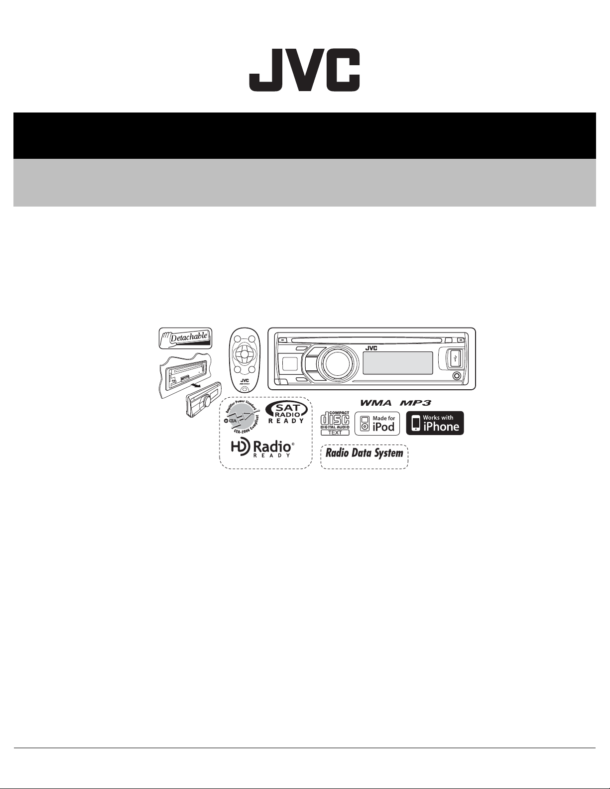
SERVICE MANUAL
CD RECEIVER
MA442<Rev.002>20098SERVICE MANUAL
KD-A605J, KD-R600J, KD-R601E, KD-R601EX,
KD-R601EY, KD-R601EU, KD-R604UI, KD-R605U,
KD-R605UN, KD-R605UT, KD-R605UH, KD-R606U,
KD-R606UN, KD-R606UT, KD-R606UH, KD-S36J
(KD-A605/KD-R600/KD-S36)
COPYRIGHT © 2009 Victor Company of Japan, Limited
Lead free solder used in the board (material : Sn-Ag-Cu, melting point : 219 Centigrade)
Lead free solder used in the board (material : Sn-Cu, melting point : 230 Centigrade)
(KD-R601)
TABLE OF CONTENTS
1 PRECAUTION. . . . . . . . . . . . . . . . . . . . . . . . . . . . . . . . . . . . . . . . . . . . . . . . . . . . . . . . . . . . . . . . . . . . . . . . . 1-7
2 SPECIFIC SERVICE INSTRUCTIONS . . . . . . . . . . . . . . . . . . . . . . . . . . . . . . . . . . . . . . . . . . . . . . . . . . . . . 1-10
3 DISASSEMBLY . . . . . . . . . . . . . . . . . . . . . . . . . . . . . . . . . . . . . . . . . . . . . . . . . . . . . . . . . . . . . . . . . . . . . . 1-10
4 ADJUSTMENT . . . . . . . . . . . . . . . . . . . . . . . . . . . . . . . . . . . . . . . . . . . . . . . . . . . . . . . . . . . . . . . . . . . . . . . 1-19
5 TROUBLESHOOTING . . . . . . . . . . . . . . . . . . . . . . . . . . . . . . . . . . . . . . . . . . . . . . . . . . . . . . . . . . . . . . . . . 1-25
COPYRIGHT © 2009 Victor Company of Japan, Limited
No.MA442<Rev.002>
2009/8
Page 2
SPECIFICATION
KD-A605/KD-R600/KD-S36
AUDIO AMPLIFIER SECTION
Power Output 20 W RMS × 4 Channels at 4 Ω and < 1% THD+N
Signal-to-Noise Ratio 80 dBA (reference: 1 W into 4 Ω)
Load Impedance 4 Ω (4 Ω to 8 Ω allowance)
Tone Control Range Bass ±12 dB (60 Hz, 80 Hz, 100 Hz, 200 Hz) Q1.0,
Q1.25, Q1.5, Q2.0
Middle ±12 dB (0.5 kHz, 1.0 kHz, 1.5 kHz, 2.5 kHz) Q0.75,
Q1.0, Q1.25
Treble ±12 dB (10.0 kHz, 12.5 kHz, 15.0 kHz, 17.5 kHz) Q
= Fixed
Frequency Response 40 Hz to 20 000 Hz
Line-Out Level/Impedance KD-A605 5.0 V/20 kΩ load (full scale)
KD-R600/KD-S36 2.5 V/20 kΩ load (full scale)
Subwoofer-Out Level/Impedance KD-A605 5.0 V /20 kΩ load (full scale)
KD-R600/KD-S36 2.5 V/20 kΩ load (full scale)
Output Impedance 1 kΩ
Other Terminal USB input jack, AUX (auxiliary) input jack, CD
changer jack, Steering wheel remote input (only for
KD-A605)
TUNER SECTION
Frequency Range FM with channel interval set to 100 kHz or
200 kHz
with channel interval set to 50 kHz 87.5 MHz to 108.0 MHz
AM with channel interval set to 10 kHz 530 kHz to 1 710 kHz
with channel interval set to 9 kHz 531 kHz to 1 602 kHz
FM Tuner Usable Sensitivity 9.3 dBf (0.8 µV/75 Ω)
50 dB Quieting Sensitivity 16.3 dBf (1.8 µV/75 Ω)
Alternate Channel Selectivity (400 kHz) 65 dB
Frequency Response 40 Hz to 15 000 Hz
Stereo Separation 40 dB
AM Tuner Sensitivity 20 µV
Selectivity 40 dB
CD PLAYER SECTION
Type Compact disc player
Signal Detection System Non-contact optical pickup (semiconductor laser)
Number of Channels 2 channels (stereo)
Frequency Response 5 Hz to 20 000 Hz
Dynamic Range 96 dB
Signal-to-Noise Ratio 98 dB
Wow and Flutter Less than measurable limit
MP3 Decoding Format: (MPEG1/2 Audio Layer 3) Max. Bit Rate: 320 kbps
WMA (Windows Media
USB Standard USB 1.1, USB 2.0
Data Transfer Rate (Full Speed) Max. 12 Mbps
Compatible Device Mass storage class
® Audio) Decoding Format Max. Bit Rate: 320 kbps
USB SECTION
87.5 MHz to 107.9 MHz
1-2 (No.MA442<Rev.002>)
Page 3
Compatible File System FAT 32/16/12
Playable Audio Format MP3/WMA
Max. Current DC 5 V 500 mA
GENERAL
Power Requirement Operating Voltage DC 14.4 V (11 V to 16 V allowance)
Grounding System Negative ground
Allowable Operating Temperature 0°C to +40°C (32°F to 104°F)
Dimensions (W × H × D): (approx.) Installation Size 182 mm × 52 mm × 160 mm (7-3/16” × 2-1/16” × 6-
5/16”)
Panel Size 188 mm × 58 mm × 6 mm (7-7/16” × 2-5/16” × 1/4”)
Mass 1.3 kg (2.9 lbs) (excluding accessories)
Design and specifications are subject to change without notice.
KD-R601
AUDIO AMPLIFIER SECTION
Maximum Power Output Front/Rear 50 W per channel
Continuous Power Output (RMS) Front/Rear 19 W per channel into 4 Ω, 40 Hz to 20 000 Hz at
no more than 0.8% total harmonic distortion.
Load Impedance 4 Ω (4 Ω to 8 Ω allowance)
Tone Control Range Bass ±12 dB (60 Hz, 80 Hz, 100 Hz, 200 Hz) Q1.0,
Q1.25, Q1.5, Q2.0
Middle ±12 dB (0.5 kHz, 1.0 kHz, 1.5 kHz, 2.5 kHz) Q0.75,
Q1.0, Q1.25
Treble ±12 dB (10.0 kHz, 12.5 kHz, 15.0 kHz, 17.5 kHz) Q
= Fixed
Frequency Response 40 Hz to 20 000 Hz
Signal-to-Noise Ratio 70 dB
Line-Out Level/Impedance 2.5 V/20 kΩ load (full scale)
Subwoofer-Out Level/Impedance 2.5 V/20 kΩ load (full scale)
Output Impedance 1 kΩ
Other Terminal USB input jack, AUX (auxiliary) input jack, CD
changer jack, Steering wheel remote input
TUNER SECTION
Frequency Range FM 87.5 MHz to 108.0 MHz
AM MW: 522 kHz to 1 620 kHz
LW: 144 kHz to 279 kHz
FM Tuner Usable Sensitivity 9.3 dBf (0.8 µV/75 Ω)
50 dB Quieting Sensitivity 16.3 dBf (1.8 µV/75 Ω)
Alternate Channel Selectivity (400 kHz) 65 dB
Frequency Response 40 Hz to 15 000 Hz
Stereo Separation 40 dB
MW Tuner Sensitivity 20 µV
Selectivity 40 dB
LW Tuner Sensitivity 50 µV
CD PLAYER SECTION
Type Compact disc player
Signal Detection System Non-contact optical pickup (semiconductor laser)
Number of Channels 2 channels (stereo)
(No.MA442<Rev.002>)1-3
Page 4
Frequency Response 5 Hz to 20 000 Hz
Dynamic Range 96 dB
Signal-to-Noise Ratio 98 dB
Wow and Flutter Less than measurable limit
MP3 Decoding Format: (MPEG1/2 Audio Layer 3) Max. Bit Rate: 320 kbps
WMA (Windows Media
USB Standard USB 1.1, USB 2.0
Data Transfer Rate (Full Speed) Max. 12 Mbps
Compatible Device Mass storage class
Compatible File System FAT 32/16/12
Playable Audio Format MP3/WMA
Max. Current DC 5 V 500 mA
Power Requirement Operating Voltage DC 14.4 V (11 V to 16 V allowance)
Grounding System Negative ground
Allowable Operating Temperature 0°C to +40°C
Dimensions (W × H × D): (approx.) Installation Size 182 mm × 52 mm× 160 mm
Mass 1.3 kg (excluding accessories)
® Audio) Decoding Format Max. Bit Rate: 320 kbps
USB SECTION
GENERAL
Panel Size 188 mm × 58 mm × 12 mm
Design and specifications are subject to change without notice.
KD-R604
AUDIO AMPLIFIER SECTION
Maximum Power Output Front/Rear 50 W per channel
Continuous Power Output (RMS) Front/Rear 19 W per channel into 4 Ω, 40 Hz to 20 000 Hz at
no more than 0.8% total harmonic distortion.
Load Impedance 4 Ω (4 Ω to 8 Ω allowance)
Tone Control Range Bass ±12 dB (60 Hz, 80 Hz, 100 Hz, 200 Hz) Q1.0,
Q1.25, Q1.5, Q2.0
Middle ±12 dB (0.5 kHz, 1.0 kHz, 1.5 kHz, 2.5 kHz) Q0.75,
Q1.0, Q1.25
Treble ±12 dB (10.0 kHz, 12.5 kHz, 15.0 kHz, 17.5 kHz) Q
= Fixed
Frequency Response 40 Hz to 20 000 Hz
Signal-to-Noise Ratio 70 dB
Line-Out Level/Impedance 2.5 V/20 kΩ load (full scale)
Subwoofer-Out Level/Impedance 2.5 V/20 kΩ load (full scale)
Output Impedance 1 kΩ
Other Terminal USB input jack, AUX (auxiliary) input jack, CD
changer jack
TUNER SECTION
Frequency Range FM 87.5 MHz to 108.0 MHz
AM 531 kHz to 1 602 kHz
1-4 (No.MA442<Rev.002>)
Page 5
FM Tuner Usable Sensitivity 9.3 dBf (0.8 µV/75 Ω)
50 dB Quieting Sensitivity 16.3 dBf (1.8µV/75 Ω)
Alternate Channel Selectivity (400 kHz) 65 dB
Frequency Response 40 Hz to 15 000 Hz
Stereo Separation 40 dB
AM Tuner Sensitivity 20 µV
Selectivity 40 dB
CD PLAYER SECTION
Type Compact disc player
Signal Detection System Non-contact optical pickup (semiconductor laser)
Number of Channels 2 channels (stereo)
Frequency Response 5 Hz to 20 000 Hz
Dynamic Range 96 dB
Signal-to-Noise Ratio 98 dB
Wow and Flutter Less than measurable limit
MP3 Decoding Format: (MPEG1/2 Audio Layer 3) Max. Bit Rate: 320 kbps
WMA (Windows Media
USB Standard USB 1.1, USB 2.0
Data Transfer Rate (Full Speed) Max. 12 Mbps
Compatible Device Mass storage class
Compatible File System FAT 32/16/12
Playable Audio Format MP3/WMA
Max. Current DC 5 V 500 mA
Power Requirement Operating Voltage DC 14.4 V (11 V to 16 V allowance)
Grounding System Negative ground
Allowable Operating Temperature 0°C to +40°C
Dimensions (W × H × D): (approx.) Installation Size 182 mm × 52 mm × 160 mm
Mass 1.3 kg (excluding accessories)
® Audio) Decoding Format Max. Bit Rate: 320 kbps
USB SECTION
GENERAL
Panel Size 188 mm ×58 mm × 6 mm
Design and specifications are subject to change without notice.
KD-R606/KD-R605
AUDIO AMPLIFIER SECTION
Maximum Power Output Front/Rear 50 W per channel
Continuous Power Output (RMS) Front/Rear 19 W per channel into 4 Ω, 40 Hz to 20 000 Hz at
no more than 0.8% total harmonic distortion.
Load Impedance 4 Ω (4 Ω to 8 Ω allowance)
Tone Control Range Bass ±12 dB (60 Hz, 80 Hz, 100 Hz, 200 Hz) Q1.0,
Q1.25, Q1.5, Q2.0
Middle ±12 dB (0.5 kHz, 1.0 kHz, 1.5 kHz, 2.5 kHz) Q0.75,
Q1.0, Q1.25
Treble ±12 dB (10.0 kHz, 12.5 kHz, 15.0 kHz, 17.5 kHz) Q
= Fixed
Frequency Response 40 Hz to 20 000 Hz
Signal-to-Noise Ratio 70 dB
Line-Out Level/Impedance 2.5 V/20 kΩ load (full scale)
(No.MA442<Rev.002>)1-5
Page 6
Subwoofer-Out Level/Impedance 2.5 V/20 kΩ load (full scale)
Output Impedance 1 kΩ
Other Terminal USB input jack, AUX (auxiliary) input jack, CD
changer jack
TUNER SECTION
Frequency Range FM 87.5 MHz to 108.0 MHz
AM 531 kHz to 1 602 kHz
FM Tuner Usable Sensitivity 9.3 dBf (0.8 µV/75 Ω)
50 dB Quieting Sensitivity 16.3 dBf (1.8 µþV/75 Ω)
Alternate Channel Selectivity (400 kHz) 65 dB
Frequency Response 40 Hz to 15 000 Hz
Stereo Separation 40 dB
AM Tuner Sensitivity 20 µV
Selectivity 40 dB
CD PLAYER SECTION
Type Compact disc player
Signal Detection System Non-contact optical pickup (semiconductor laser)
Number of Channels 2 channels (stereo)
Frequency Response 5 Hz to 20 000 Hz
Dynamic Range 96 dB
Signal-to-Noise Ratio 98 dB
Wow and Flutter Less than measurable limit
MP3 Decoding Format: (MPEG1/2 Audio Layer 3) Max. Bit Rate: 320 kbps
WMA (Windows Media
USB Standard USB 1.1, USB 2.0
Data Transfer Rate (Full Speed) Max. 12 Mbps
Compatible Device Mass storage class
Compatible File System FAT 32/16/12
Playable Audio Format MP3/WMA
Max. Current DC 5 V 500 mA
Power Requirement Operating Voltage DC 14.4 V (11 V to 16 V allowance)
Grounding System Negative ground
Allowable Operating Temperature 0°C to +40°C
Dimensions (W × H × D): (approx.) Installation Size 182 mm × 52 mm × 160 mm
Mass 1.3 kg (excluding accessories)
® Audio) Decoding Format Max. Bit Rate: 320 kbps
USB SECTION
GENERAL
Panel Size 188 mm × 58 mm × 6 mm
Design and specifications are subject to change without notice.
1-6 (No.MA442<Rev.002>)
Page 7
1.1 Safety Precautions
SECTION 1
PRECAUTION
!
!
Burrs formed during molding may be left over on some parts of the chassis. Therefore,
pay attention to such burrs in the case of preforming repair of this system.
Please use enough caution not to see the beam directly or touch it in case of an
adjustment or operation check.
(No.MA442<Rev.002>)1-7
Page 8
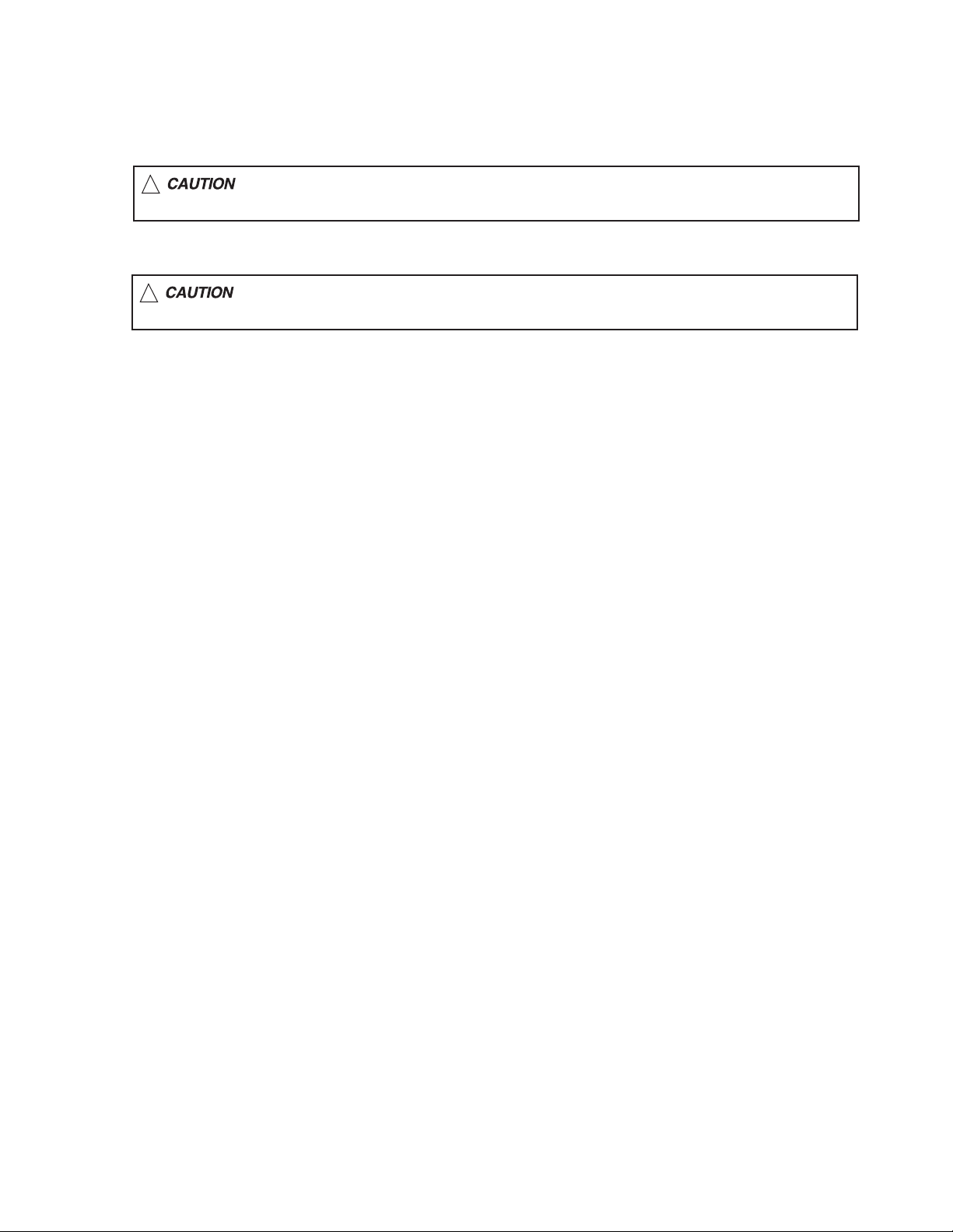
1.2 Preventing static electricity
Electrostatic discharge (ESD), which occurs when static electricity stored in the body, fabric, etc. is discharged, can destroy the laser
diode in the traverse unit (optical pickup). Take care to prevent this when performing repairs.
1.2.1 Grounding to prevent damage by static electricity
Static electricity in the work area can destroy the optical pickup (laser diode) in devices such as laser products.
Be careful to use proper grounding in the area where repairs are being performed.
(1) Ground the workbench
Ground the workbench by laying conductive material (such as a conductive sheet) or an iron plate over it before placing the
traverse unit (optical pickup) on it.
(2) Ground yourself
Use an anti-static wrist strap to release any static electricity built up in your body.
(caption)
Anti-static wrist strap
1M
Conductive material
(conductive sheet) or iron plate
(3) Handling the optical pickup
• In order to maintain quality during transport and before installation, both sides of the laser diode on the replacement optical
pickup are shorted. After replacement, return the shorted parts to their original condition.
(Refer to the text.)
• Do not use a tester to check the condition of the laser diode in the optical pickup. The tester's internal power source can easily
destroy the laser diode.
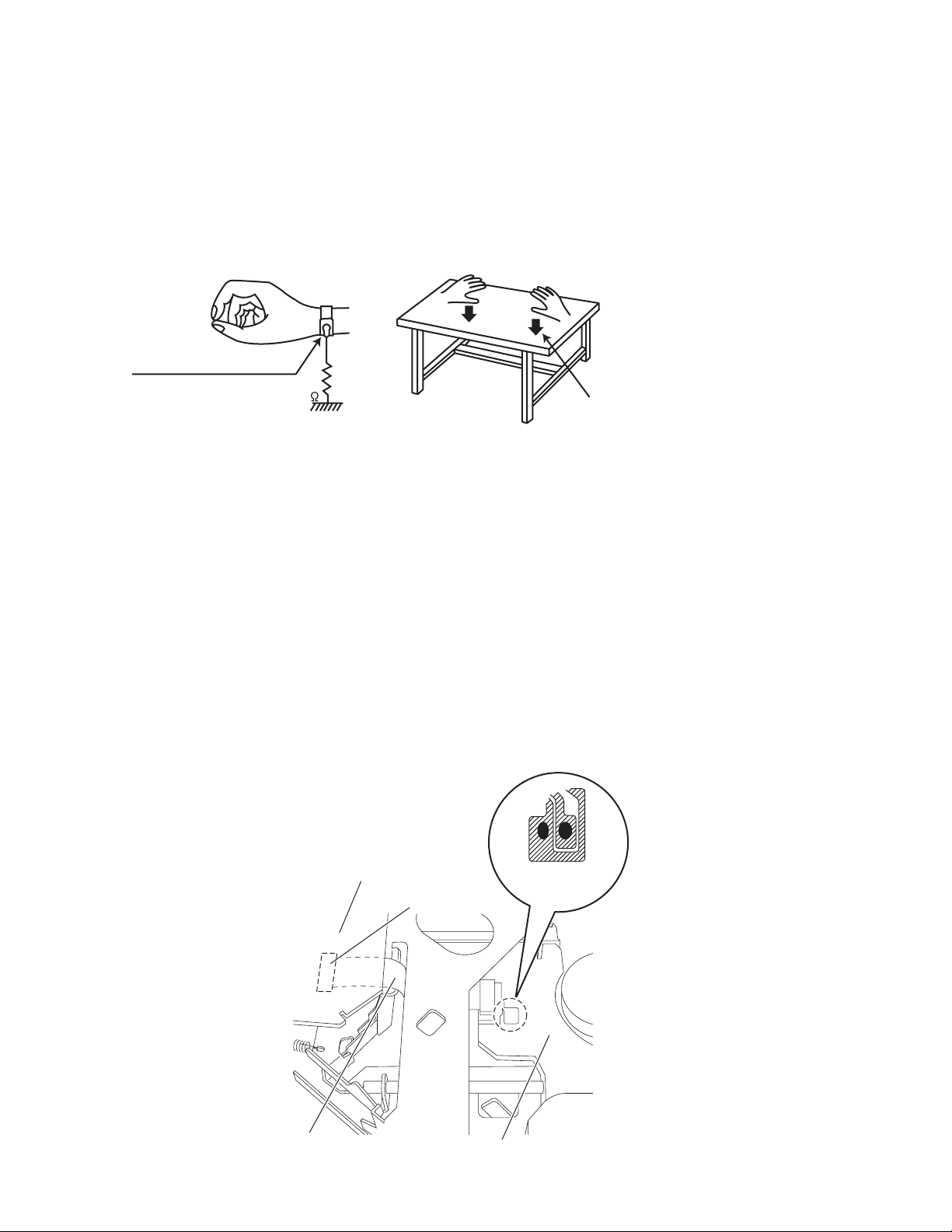
1.3 Handling the traverse unit (optical pickup)
(1) Do not subject the traverse unit (optical pickup) to strong shocks, as it is a sensitive, complex unit.
(2) Cut off the shorted part of the flexible cable using nippers, etc. after replacing the optical pickup. For specific details, refer to the
replacement procedure in the text. Remove the anti-static pin when replacing the traverse unit. Be careful not to take too long a
time when attaching it to the connector.
(3) Handle the flexible cable carefully as it may break when subjected to strong force.
(4) It is not possible to adjust the semi-fixed resistor that adjusts the laser power. Do not turn it.
1.4 Attention when traverse unit is decomposed
*Please refer to "Disassembly method" in the text for the pickup unit.
• Apply solder to the short land before the card wire is disconnected from the connector on the pickup unit.
(If the card wire is disconnected without applying solder, the pickup may be destroyed by static electricity.)
• In the assembly, be sure to remove solder from the short land after connecting the card wire.
1-8 (No.MA442<Rev.002>)
Mechanism control board
CN102
Flexible wire
Short land section
Pickup
Page 9
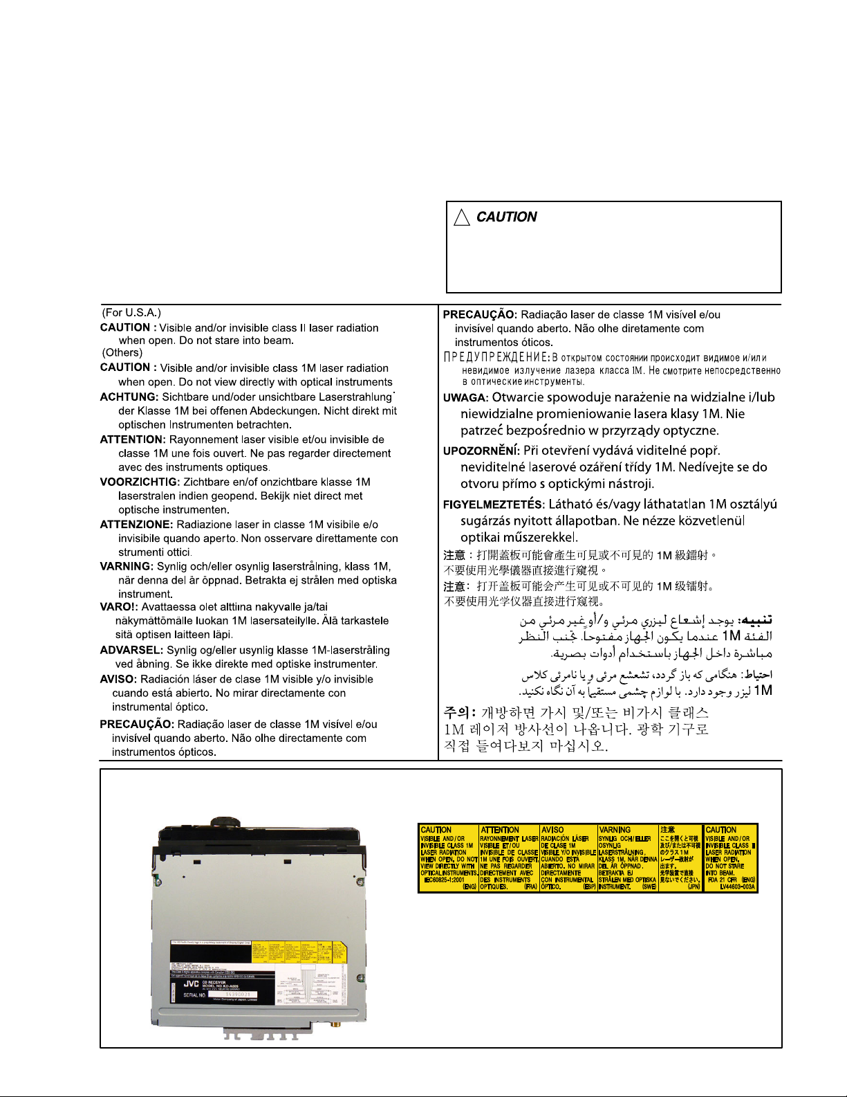
1.5 Important for laser products
1.CLASS 1 LASER PRODUCT
2.CAUTION :
(For U.S.A.) Visible and/or invisible class II laser radiation
when open. Do not stare into beam.
(Others) Visible and/or invisible class 1M laser radiation
when open. Do not view directly with optical instruments.
3.CAUTION : Visible and/or invisible laser radiation when
open and inter lock failed or defeated. Avoid direct
exposure to beam.
4.CAUTION : This laser product uses visible and/or invisible
laser radiation and is equipped with safety switches which
prevent emission of radiation when the drawer is open and
the safety interlocks have failed or are defeated. It is
dangerous to defeat the safety switches.
5.CAUTION : If safety switches malfunction, the laser is able
to function.
6.CAUTION : Use of controls, adjustments or performance of
procedures other than those specified here in may result in
hazardous radiation exposure.
!
Please use enough caution not to
see the beam directly or touch it
in case of an adjustment or operation
check.
REPRODUCTION AND POSITION OF LABELS and PRINT
WARNING LABEL and PRINT
(No.MA442<Rev.002>)1-9
Page 10
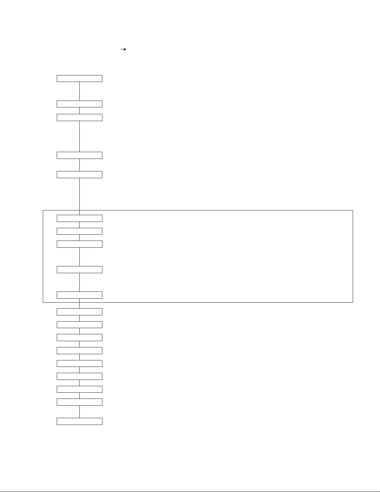
SECTION 2
SPECIFIC SERVICE INSTRUCTIONS
2.1 Identification method
Supported reduction in cost, and board contents was changed.
A set put the following label on is an object.
Front side
Top view
Label position
Change pwb parts
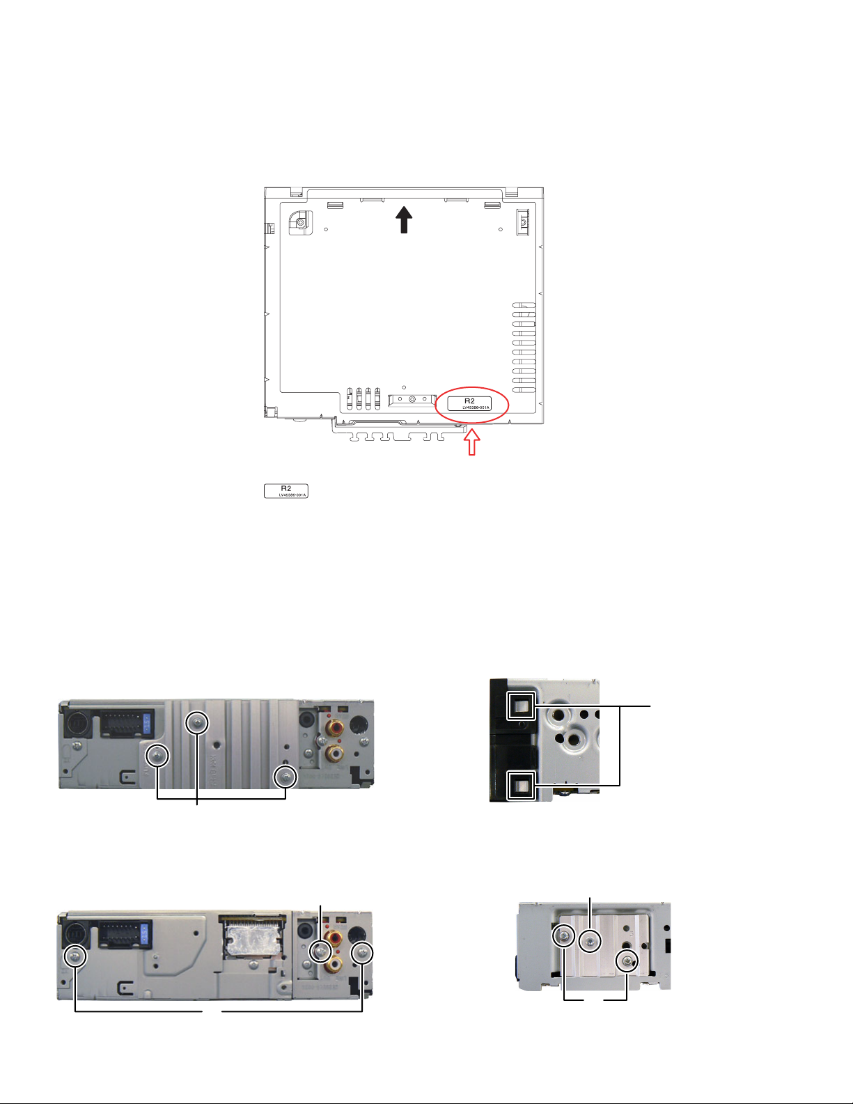
SECTION 3
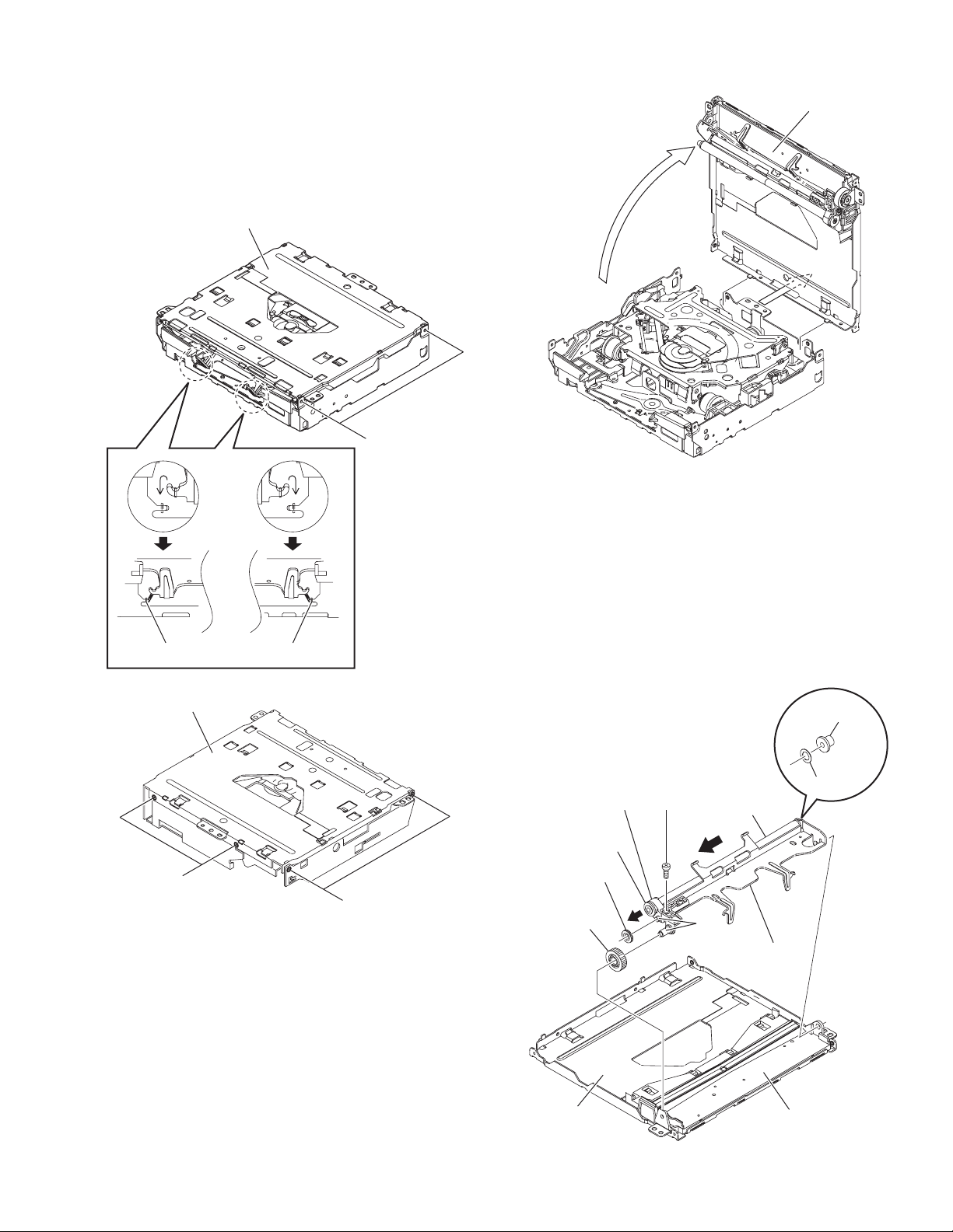
DISASSEMBLY
3.1 Main body (Used figure are KD-A605)
3.1.1 Removing the Bottom chassis (See Fig.1, 2)
(1) Remove the three screws A attaching the Heat sink. (See
Fig.1)
A
Fig.1
(2) Remove the two screws B and one screw C attaching the
Bottom chassis. (See Fig.2)
C
3.1.2 Removing the Front chassis (See Fig.3)
(1) Disengage four hooks a engaged both side of the Front
chassis.
hook a
Fig.3
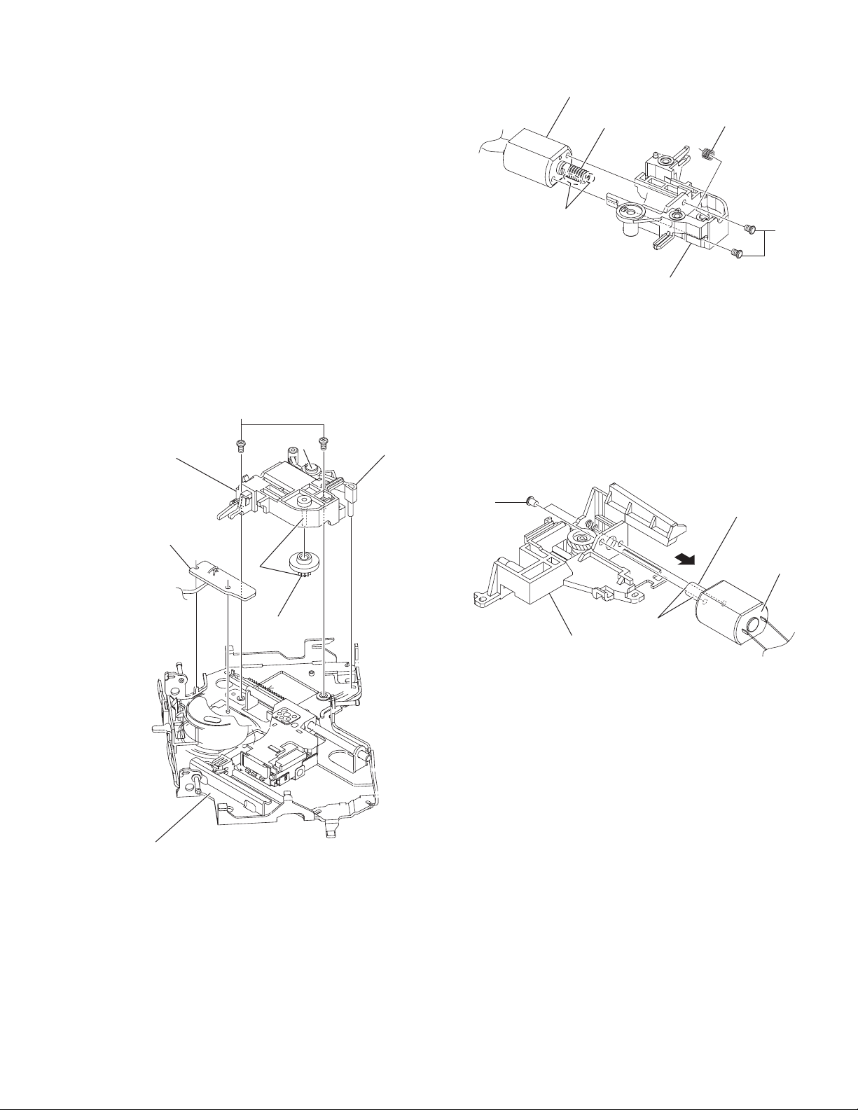
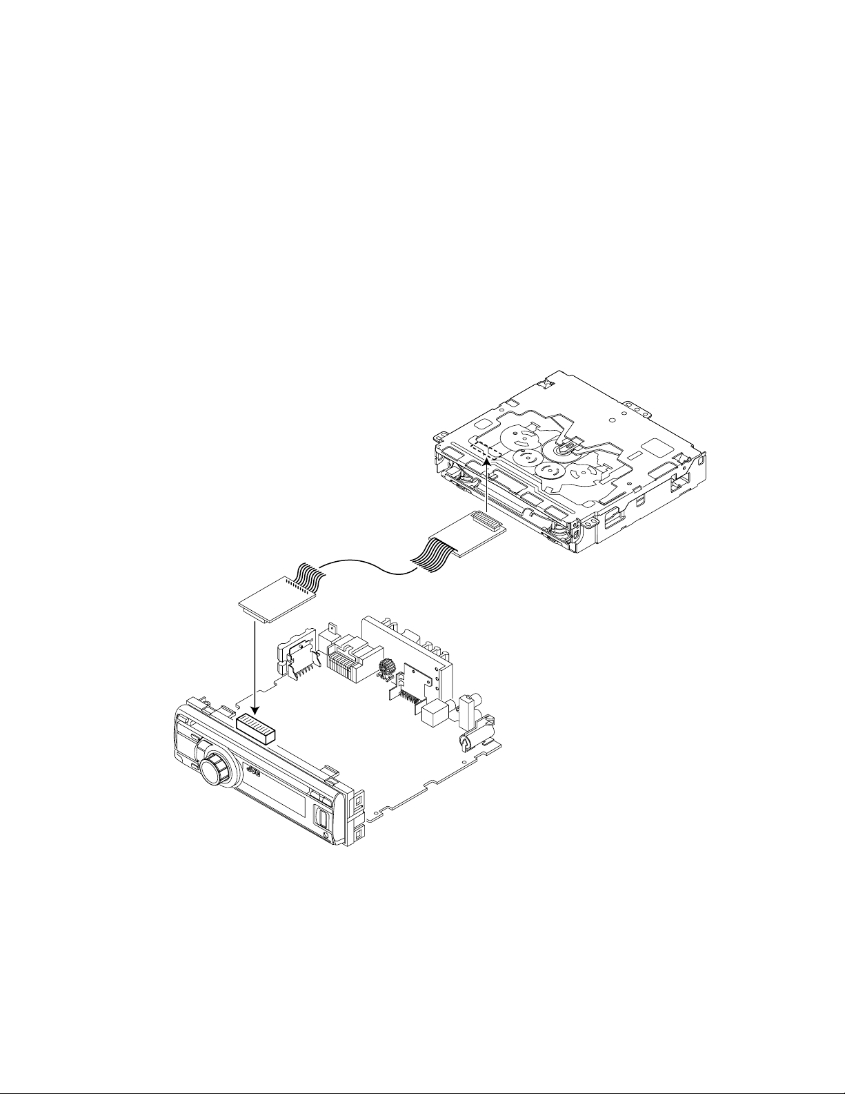
3.1.3 Removing the Main board (See Fig.4 to 6)
(1) Remove the two screws D and one screw E attaching the
Side plate. (See Fig.4)
E
B
Fig.2
(3) Slide to backward and the remove the Bottom chassis.
1-10 (No.MA442<Rev.002>)
D
Fig.4
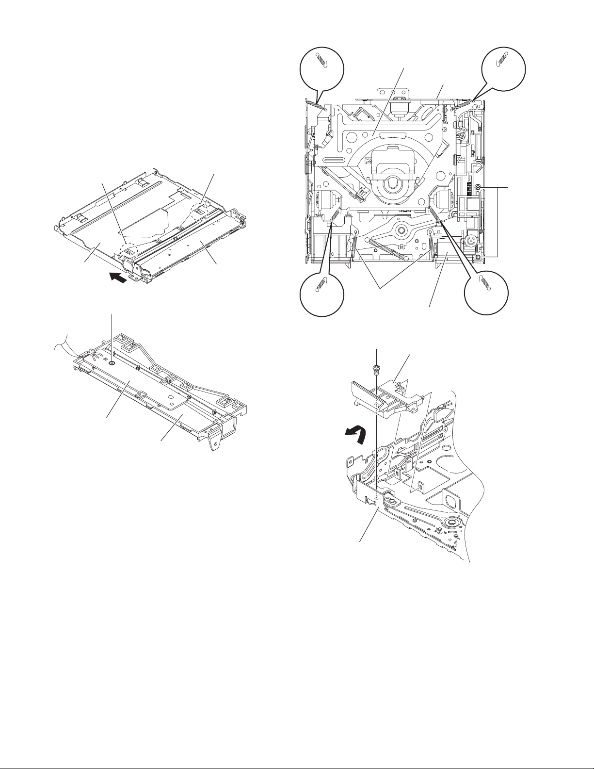
Page 11
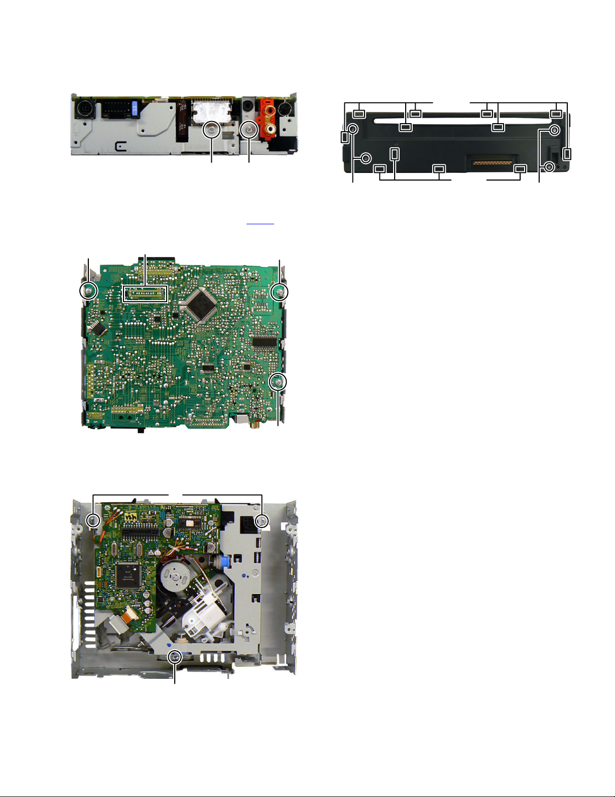
(2) Remove the one screw F attaching the Power IC. (See
Fig.5)
(3) Remove the one screw G attaching the OE holder. (See
Fig.5)
3.1.5 Removing the Switch board (See Fig.8)
(1) Remove the volume knob.
(2) Remove the four screws K attaching the Rear cover.
(3) Disengage eleven hooks b engaged Rear cover.
hook b
FG
Fig.5
(4) Remove the three screws H attaching the Main board. (See
Fig.6)
(5) Disconnect the board to board connector CN501
ed Main board and CD mechanism. (See Fig.6)
H
CN501
connect-
H
H
Fig.6
3.1.4 Removing the CD mechanism (See Fig.7)
(1) Remove the three screws J attaching the CD mechanism.
hook b
KK
Fig.8
J
J
Fig.7
(No.MA442<Rev.002>)1-11
Page 12
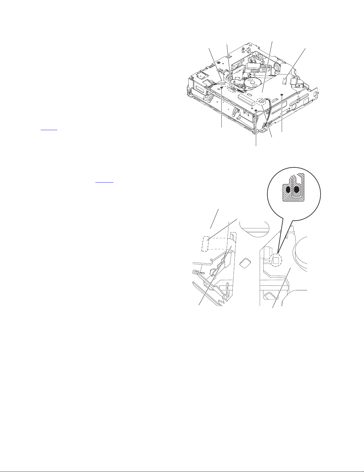
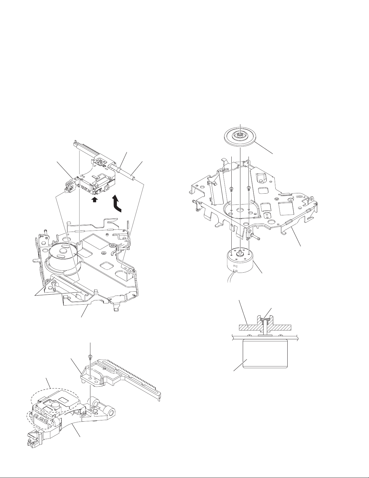
3.2 CD MECHANISM assembly section
• Remove the CD MECHANISM assembly from the main body.
Removing the MECHANISM CONTROL BOARD
3.2.1
1
assembly (See Fig.
(1)
From the bottom side of CD MECHANISM assembly,
remove the solders from the soldered sections (
c
) on the MECHANISM CONTROL BOARD assembly.
(See Fig.
(2) Remove the three screws A attaching the MECHANISM
CONTROL BOARD assembly. (See Fig.1.)
(3) Solder the short land sections on the pickup. (See Fig.2.)
Caution:
• Solder the short land sections on the pickup before
•
1
.)
disconnecting the flexible wire from the connector
on the MECHANISM CONTROL BOARD as-
CN102
sembly.
If the card wire is disconnected without attaching
solder, the pickup may be destroyed by static
electricity. (See Fig.2.)
When attaching the MECHANISM CONTROL
BOARD assembly, remove the solders from the
short land sections after connecting the flexible
wire to the connector CN102
CONTROL BOARD assembly.
and 2)
a, b
and
on the MECHANISM
Mechanism
a
b
control board
CN102
A
A
c
A
Fig.1
Mechanism control board
CN102
Flexible wire
Short land section
Pickup
Fig.2
1-12 (No.MA442<Rev.002>)
Page 13
3.2.2 Removing the top cover (See Fig.3 to 5)
• Remove the MECHANISM CONTROL BOARD assembly.
(1) From the front side of the CD MECHANISM assembly,
change the hook position of the two roller springs. (See
Fig.3.)
(2) From the side of the CD MECHANISM assembly, remove
the six screws B attaching the top cover. (See Fig.3 and 4.)
(3) Take out the top cover in an upward direction. (See Fig.5.)
Top cover
B
Roller spring Roller spring
Fig.3
Top cover
Top cover
Fig.5
3.2.3 Removing the roller (See Fig.6)
• Remove the MECHANISM CONTROL BOARD assembly and
top cover.
(1) From the bottom side of the top cover, remove the screw C
attaching the gear holder.
(2) Remove the R.holder assembly from disc plate, and then
take out the roller from R.holder assembly in the direction
of the arrow.
Reference:
When attaching the R.ACT gear (2) and R.ACT gear (3),
apply grease to the section d of R.holder assembly.
Roller coller
B
Fig.4
B
Gear holder
Roller gear
R.ACT gear(3)
R.ACT gear(2)
Top cover
C
d
R.holder assembly
Fig.6
Washer
Roller
Disc plate
(No.MA442<Rev.002>)1-13
Page 14
3.2.4 Removing the PHOTO BOARD assembly (See Fig.7
and 8)
• Remove the MECHANISM CONTROL BOARD assembly and
top cover.
From the bottom side of the top cover, release the
(1)
projection
7
Fig.
(2) Take out the disc plate in the direction of the arrow. (See
Fig.7.)
(3) From the reverse side of the disc plate, remove the screw
D attaching the PHOTO BOARD assembly. (See Fig.8.)
e
from the notch of the disc plate. (See
.)
e
e
SUS
spring
Mechanism section
Mecha frame
SUS
spring
E
Top cover
Fig.7
Disc plate
D
Photo board
Disc plate
Fig.8
3.2.5 Removing the mechanism section (See Fig.9 and 10)
• Remove the MECHANISM CONTROL BOARD assembly and
top cover.
(1)
From the top side of the CD MECHANISM assembly,
remove the two screws
assembly. (See Fig.
(2) Remove the two roller springs on the top side of the mecha
frame. (See Fig.9.)
(3) Remove the four SUS springs on the top side of the mecha
frame. (See Fig.9.)
(4) Remove the link spring on the top side of the mecha frame.
(See Fig.10.)
(5) Release section f of the three dampers from the mecha
frame. (See Fig.10.)
Reference:
When attaching the roller spring and SUS spring, keep
direction before remove.
Move the slide cam (R) assembly in the direction of the
(6)
arrow, and then take out the mechanism section in an
upward direction. (See Fig.
Reference:
When attaching the mechanism section, apply grease to
the section g. (See Fig.10.)
E
attaching the loading motor
9
.)
10.)
SUS
spring
Roller spring
Loading motor assembly
Fig.9
F
Cam cover
Mecha frame
Fig.10
SUS
spring
1-14 (No.MA442<Rev.002>)
Page 15
3.2.6 Removing the slide cam (L) (See Fig.11 to 13)
• Remove the MECHANISM CONTROL BOARD assembly, top
cover and mechanism section.
(1) From the top side of the mecha frame, remove the screw F
attaching the cam cover. (See Fig.11.)
Take out the cam cover from mecha frame in an upward
(2)
11
F
.)
Cam cover
direction. (See Fig.
(3) Take out the slide cam (L) in the direction of the arrow.
(See Fig.12.)
Reference:
When attaching the slide cam (L), apply grease to the
section h. (See Fig.13.)
Slide cam(L)
Mecha frame
Fig.12
h
Slide cam(L)
h
Mecha frame
Fig.11
h
h
Slide cam(L)
h
Fig.13
h
h
h
(No.MA442<Rev.002>)1-15
Page 16
3.2.7 Removing the F.lock lever and slide cam (R) (See
Fig.14 and 15)
• Remove the MECHANISM CONTROL BOARD assembly, top
cover and mechanism section.
(1) From the top side of the mecha frame, take out the slide
cam (R) assembly in an upward direction. (See Fig.14.)
(2) Rotate the F.lock lever in the direction of the arrow 1, and
then take out the direction of the arrow 2. (See Fig.14.)
Reference:
When attaching the slide cam (R) assembly, the f.lock
lever and the link arm apply grease to the section
14
(See Fig.
and 15.)
h
Slide cam(R) assembly
h
F.lock lever
2
1
h
h
3.2.8 Removing the damper (See Fig.16)
• Remove the MECHANISM CONTROL BOARD assembly, top
cover and mechanism section.
From the mechanism section, pull out the three dampers in the
direction of the arrow.
Reference:
Before inserting the shaft to the dampers, apply IPA to the
pocket j of damper.
.
Damper (Gray)
Damper (Brown)
j
j
Damper (Brown)
j
Fig.16
Mecha frame
h
h
h
h
Fig.14
Link arm
Slide cam(R) assembly
h
h
h
Slide cam(R) assembly
Fig.15
3.2.9 Removing the clamper assembly (See Fig.17)
• Remove the MECHANISM CONTROL BOARD assembly, top
h
cover and mechanism section.
(1) From the top side of the mechanism section, release the
clamper spring.
(2) Move the clamper assembly in the direction of the arrow,
and then release the joints (k and m).
Take out the clamper assembly from the T.M chassis
(3)
assembly.
h
Clamper assembly
Clamper spring
k
1-16 (No.MA442<Rev.002>)
T.M. chassis assembly
m
Fig.17
Page 17
3.2.10 Removing the feed motor (See Fig.18 and 19)
r
• Remove the MECHANISM CONTROL BOARD assembly, top
cover, mechanism section and clamper assembly.
(1) From the bottom side of the T.M chassis assembly, remove
the two screws G attaching the feed motor assembly. (See
Fig.18.)
Remove the two screws H attaching the feed motor to
(2)
19
f.motor holder. (See Fig.
Reference:
When attaching the f. wheel gear, trigger arm and feed
motor, apply grease to the sections (n, p and q). (See
Fig.18 and 19.)
.)
Feed motor
F.worm gear
q
Comp. spring
H
3.2.11 Removing the SWITCH BOARD assembly (See
Fig.18)
• Remove the MECHANISM CONTROL BOARD assembly, top
cover, mechanism section, clamper assembly and feed motor
assembly.
From the bottom side of the T.M chassis assembly, take out
the SWITCH BOARD assembly in an upward direction from
T.M chassis assembly.
G
Feed motor assembly
Switch board
p
n
F.wheel gear
Trigger arm
F.motor holder
Fig.19
3.2.12 Removing the loading motor (See Fig.20)
• Remove the MECHANISM CONTROL BOARD assembly, top
cover, mechanism section and clamper assembly.
(1) From the right side of the L.M base assembly, remove the
two screws J attaching the loading motor.
(2) Take out the loading motor in the direction of the arrow
from the L.M base assembly.
Reference:
When attaching the loading motor, apply grease to the
section r.
J
r
L.M. base assembly
Fig.20
L.worm gear
Loading moto
T.M. chassis assembly
Fig.18
(No.MA442<Rev.002>)1-17
Page 18
3.2.13 Removing the pickup assembly (See Fig.21 to 22)
• Remove the MECHANISM CONTROL BOARD assembly, top
cover, mechanism section, clamper assembly and feed motor
assembly.
Caution:
• Do not touch section u on the pickup assembly. (See Fig.21
and 22.)
(1) From the bottom side of the T.M chassis assembly, move
the pickup assembly in the direction of the arrow from the
T.M chassis assembly. (See Fig.21.)
(2) Pull out the main shaft. (See Fig.21.)
(3) Remove the screw K attaching the pickup to the rack plate.
(See Fig.22.)
Reference:
When attaching the loading motor, apply grease to the
sections s and t. (See Fig.21.)
3.2.14 Removing the spindle motor (See Fig.23 and 24)
Remove the MECHANISM CONTROL BOARD assembly,
•
top cover, mechanism section, clamper assembly, feed motor
assembly and pickup assembly.
(1) From the top side of the T.M chassis assembly, remove the
CD T.table assembly from the spindle motor. (See Fig.23.)
(2) Remove the two screws L attaching the spindle motor.
(See Fig.23.)
(3) Take out the spindle motor from the bottom side of the T.M
chassis assembly. (See Fig.23.)
Reference:
When attaching the CD T.table assembly to the spindle
motor shaft, apply loctite 460 to inside the CD T.table
assembly. (See Fig.24.)
Pick up assembly
s
T.M. chassis assembly
u
Fig.21
t
Main shaft
LL
Spindle motor
Fig.23
CD T.table assembly
CD T.table assembly
T.M.chassis assembly
Loctite
Rack plate
u
Pick up
1-18 (No.MA442<Rev.002>)
K
Spindle motor
Fig.24
Fig.22
Page 19
SECTION 4
ADJUSTMENT
4.1 Test instruments required for adjustment
(1) Digital oscilloscope (100MHz)
(2) Digital tester
(3) Test Disc
(4) Extension cable : EXTCD004-28P
4.2 Standard measuring conditions
Power supply voltage DC14.4V(10.5 to 16V)
Load impedance 20K ohm (2 Speakers connection)
Output Level Line out 2.5V (Vol. MAX)
4.5 How to connect the extension cable for adjusting
Caution:
Be sure to attach the heat sink and rear bracket onto the power amplifier IC and regulator IC respectively, before supply the power.
If voltage is applied without attaching these parts, the power amplifier IC and regulator IC will be destroyed by heat.
Extension cable
EXTCD004-28P
4.3 Standard volume position
Balance and Bass &Treble volume : lndication"0"
Loudness : OFF
4.4 Dummy load
Exclusive dummy load should be used for AM,and FM.
For FM dummy load, there is a loss of 6dB between SSG output and antenna input.
The loss of 6dB need not be considered sincedirect reading of
figures are applied in this working standard.
(No.MA442<Rev.002>)1-19
Page 20
4.6 Service mode
Operating key: [MENU] [DOWN] (3 sec)
Navigation key : Press [SEL] in any main display item to select that option.
Volume Knob Turn: forward and backward selection
INIT ALL Initialize all data to factory shipment state.
SIRIUS RST SIRIUS Soft Reset
XM RST XM Soft Reset (It clears all contents of built-in RAM and EEPROM, and performs software reset.)
HD RST HD Soft Reset (It clears all contents of built-in RAM and EEPROM, and performs software reset.)
DAB RST DAB Soft Reset (It clears all contents of built-in RAM and EEPROM, and performs software reset.)
BT RST BT Soft Reset (It clears all contents of built-in RAM and EEPROM, and performs software reset.)
RUNNING MODE 1 CD4 module running mode 1 (Only factory use)
(It clears all the contents of built-in RAM and EEPROM, and performs software reset.)
* Active at the time of SIRIUS connection.
* Active at the time of XM connection.
* Active at the time of HD connection.
* Active at the time of DAB connection.
* Active at the time of BT connection.
MODE 2
Note : A disc is inserted, and it is displayed only at the time of CD function.
CHECK MODE NORMAL PLAY Disc operation & playback. (playback from starting position)
CURENT ##** Laser Electric Current Value
JITTER #### Jitter Value
OUT TRK OFF Tracking off at CD outermost lap.
INN TRK OFF Tracking off at CD innermost lap.
CD LASER ON CD Laser Illumination and electric current.
CURENT ##** Laser Electric Current Value
JITTER #### Jitter Value
STOP Disc stop, LD(Laser) OFF
CD ERROR Display the CD Error past record stored in EEPROM.
TOTAL-****: Total error count
E#xxyyyy : Latest 3 errors recorded. #: counter xx: error code yyyy: detailed error code
0#xxyyyy : The first 5 errors recorded. #: counter xx: error code yyyy: detailed error code
Note: Shifting among the above items is done by using "FF" or "REW" key.
CLR CDERROR Clear CD Error history from EEPROM.
CD4 module running mode 2 (Only factory use)
##: Initial value **: Current value
Note: Pressing "FF" or "REW" key to switch between current value
and jitter value display.
##: Initial value **: Current value
Note: Pressing "FF" or "REW" key to switch between current value
aand jitter value display.
CH ERROR Display the CH Error past record stored in EEPROM
CLR CHERROR Clear CH Error history from EEPROM.
TSUBUYAKI Only engineer use
1-20 (No.MA442<Rev.002>)
* Active at the time of CD CHANGER/ iPod (J-BUS) connection
E#xxyyyy : Latest 3 errors recorded. #: counter xx: error code yyyy: detailed error code
0#xxyyyy : The first 5 errors recorded. #: counter xx: error code yyyy: detailed error code
Note: Shifting among the above items is done by using "FF" or "REW" key.
* Active at the time of CD CHANGER/ iPod (J-BUS) connection
Page 21
4.7 Tuner service mode
Key operation (FM, AM and DAB mode)
Enter service mode: [SEL] [MENU] (3 sec)
Exit service mode: press [ENTER] (SEL) key.
Go to next item: press [DISP] key
Back to previous item: press [BACK] key
VER=#*** MICON version display
CD4V#### CD4 module version display.
######## Tuner device and version identification display
TINJ= ## Tuner injection indicator
SPI=#### FOR DAB ONLY
# indicates destination: J=USA, U=OTHERS (eg. ASIA), R=EUROPE, E=EASTERN EUROPE
*** indicates version No.
Display :TOM V1 for TOMIC V1 tuner.
Display :TOM V2 for TOMIC V2 tuner.
Display :ATOM V2 for ATOMIC V2 tuner.
Display: ATOM V3 for ATOMIC V3 tuner.
"##" indicates current tuner injection.
To link SID display that DAB receives and FM station (Search PI), the reception situation of DAB is
displayed.
"####" indicates SID code.
FOR RDS ONLY
PI =#### PI display of receiving station, "####" indicates PI code.
PTY=## PTY display of receiving station (00~29), "##" indicates PTY code.
TP=#TA=* TP, TA display of receiving station
"#" indicates TP ON/OFF: 1=ON; 0=OFF;
"*" indicates TA ON/OFF: 1=ON; 0=OFF.
MS=#DI=* M/S, DI display of receiving station
"#" indicates M/S ON/OFF: 1=ON; 0=OFF;
"*" indicates DI ON/OFF: 1=ON; 0=OFF.
AF=#### Display the contents of AF memory (by scrolling) "####" indicate AF frequencies.
LEV= ##H Field strength indicator.
U&W= ##H Adjacent and Multipath noise level indicator.
IFC= ##H IF COUNTER result indicator.
IFBW= # FM IF filter bandwidth indicator.
RFAGC=## FM RF AGC resulting attenuation.
IFAGC=## FM IF AGC resulting attenuation.
##** CLOCK display of receiving station (Original DISP key operation)
######## FOR RDS ONLY
PS NAME display of receiving station (Original DISP key operation)
##### FREQUENCY display of receiving station (Original DISP key operation)
(No.MA442<Rev.002>)1-21
Page 22
4.8 Error code
4.8.1 Mechanical Error Detail Codes
Condition Details Error Code Detail Code
LOADING Error Error without SW change in LOAD when time-out is done
B1 time out
C1 time out
B2 time out
EJECT Error Error without SW change in EJECT when time-out is done.
B1 time out
C2 time out
B2 time out
FORCE EJECT Error Transition to Force EJECT waiting or Force EJECT transition from error by abnormal SW.
E1 FORCE EJECT ERROR When detect abnormal SW from the state of NO DISC 01 0041
E2 FORCE EJECT ERROR When detect abnormal SW from the state with DISC forward in LOAD. 01 0042
E3 FORCE EJECT ERROR When detect abnormal SW from the initial state. 01 0043
E5 FORCE EJECT ERROR
E7 FORCE EJECT ERROR
E8 FORCE EJECT ERROR
E9 FORCE EJECT ERROR
Case 1 When DISC was extracted or fall in EJECT END and EJECT START. 09 0031
Case 2 When DISC is pushed in EJECT END. 09 0032
When there is no change in the state of the switch from the state with
DISC forward.
When there is no change in the state of the switch from the state that
DISC is drawn in a half.
When there is no change in the state of the switch from the state that
DISC is in the interior.
When there is no change in the state of the switch from the state that
DISC is in the interior.
When there is no change in the state of the switch from the state that
DISC is drawn in a half.
When there is no change in the state of the switch in EJECT from initial
LOAD ERROR.
When detect abnormal SW from the state that half DISC is drawn in
LOAD and EJECT.
When detect abnormal SW from the state that DISC is in the interior in
LOAD and EJECT.
When receive Force EJECT key after it makes an error from Force
EJECT.
When receive Force EJECT key after it makes an error from LOAD
error or EJECT error.
Error in Running mode
09 0011
09 0012
09 0015
01 0023
01 0026
01 0027
01 0045
01 0047
01 0048
01 0049
4.8.2 Disc error code
Condition Details Error Code Detail Code
TOC READING Error When it hasn't completed CD TOC reading. 84 0059
1'st track access Error
Last track access Error
NO DISC judgment It be judged NO DISC. 80 0090
NO DISC with start failure Not possible to start. 80 0091
Stopped with no playback When it was stopped in playback in the running mode. 80 0093
Logical format NG
1-22 (No.MA442<Rev.002>)
It doesn't end even if the first track access passes 30sec after the TOC
reading ends in the running mode.
It doesn't end even if the last track access passes 30sec after the first
track ends in the running mode.
Analysis of logical format is impossible or it does not correspond to
logical formats.
80 0060
80 0061
80 0094
Page 23
4.8.3 CD changer mechanism error code
Condition Details Error Code Detail Code
Tray eject error
1.TRAYINSW time over
(TRAYINSW:L, TRAYOUTSW:H)
2.TRAYOUTSW time over
(TRAYINSW:H, TRAYOUTSW:H)
3.TRAYIN/OUTSW time over
(TRAYINSW:L, TRAYOUTSW:L)
4.MAGINSW:L→H
Tray return error
1.TRAYOUTSW time over
(TRAYINSW:H, TRAYOUTSW:L)
2.TRAYINSW time over
(TRAYINSW:H, TRAYOUTSW:H)
3.TRAYIN/OUTSW time over
(TRAYINSW:L, TRAYOUTSW:L)
4.MAGINSW:L→H
Lifter up error
1.WAIT position time over
2.WAIT position time over
3.WAIT position time over
Lifter down error
1.WAIT position time over
2.WAIT position time over
3.WAIT position time over
Chucking error
1.Play position time over
2.Play position time over
3.Play position time over
Unchucking error
1.WAIT position time over
2.WAIT position time over
3.WAIT position time over
Eject error
1.Eject position time over
2.Eject position time over
3.MAGINSW time over
Initialize error
1.Mechanism SW NG error
2.Absolute position time over
Tray motor time over
Tray motor does not operate
Tray stops
TRAYINSW NG etc
Magazine is ejected while Tray is being returned
Tray motor time over
Tray motor does not operate
Tray stops
TRAYOUTSW NG etc
Magazine is ejected while Tray is being returned
Position motor time over
Position motor does not operate
Position is not stable in fine adjustment mode
Other condition
Position motor time over
Position motor does not operate
Position is not stable in fine adjustment mode
Other condition
Position motor time over
Position motor does not operate
Position is not stable in fine adjustment mode
Other condition
Position motor time over
Position motor does not operate
Position is not stable in fine adjustment mode
Other condition
Eject cannot be carried out
Position motor does not operate
Improper EJECT position *
Magazine is not ejected
TRAYINSW and TRAYOUTSW are L
Position is not stable in absolute position
03
03
03
03
03
03
03
03
02
02
02
02
02
02
02
02
02
02
02
02
02
02
01
03
02
0011
0012
0013
0014
0016
0017
0018
0019
0021
0022
0023
0026
0027
0028
0031
0032
0033
0036
0037
0038
0041
0042
0043
0046
0047
*"Position is not stable in WAIT position," "Position is not stable in PLAY position," and "Position is not stable in absolute position,"
and "Improper EJECT are all Position Motor TIME OVER.
(No.MA442<Rev.002>)1-23
Page 24
4.8.4 CD changer disc error code
Condition Details Error code Detail code
Pickup movement error
1.Time over of pickup movement in
an inner direction (10s)
2.Time over of pickup movement in
an outer direction (10s)
Focus search error
Focus is not adjusted by 3-round focus search
Tracking balance adjustment error.
Time over(1s)
TOC area search error
Time over (10s)
Focus balance adjustment error
Time over(2s)
Focus gain adjustment error
Time over(0.6s)
Tracking gain adjustment error
Time over(0.6s)
TOC read error TIME over(30s) TOC read operation is not finished after 30s 84 0059
First track access error
Time over(10s)
Last track access error
Time over(10s)
Q code read error
Time over(0.6s)
Time over at PUBWD and PUFWD by monitoring RESET SW
Pickup cannot move in an inner direction
RESET SW is not on
Pickup cannot move in an outer direction
RESET SW is not off
When focus is not adjusted by 3-round(1set) focus search
after disc change or focus shock, the result is NG 81 0053
Tracking balance adjustment is not finished 1s after adjustment
command(TBA) is executed
TOC area search is not finished after 10s
Focus balance adjustment is not finished 2s after adjustment
command(FBA) is executed
Focus gain adjustment error is not finished 0.6s after adjustment
command(FGA) is executed
Tracking gain adjustment error is not finished 0.6s after adjustment command(TGA) is executed
First track access is not finished 10s after TOC reading is finished
Last track access is not finished 10s after first track in running
mode
Q code is not read for 0.6s during playback of TOC and program
area
04
04
82 0054
80 0055
82 0056
82 0057
82 0058
80 0060
80 0061
80 0062
0051
0052
1-24 (No.MA442<Rev.002>)
Page 25
SECTION 5
TROUBLESHOOTING
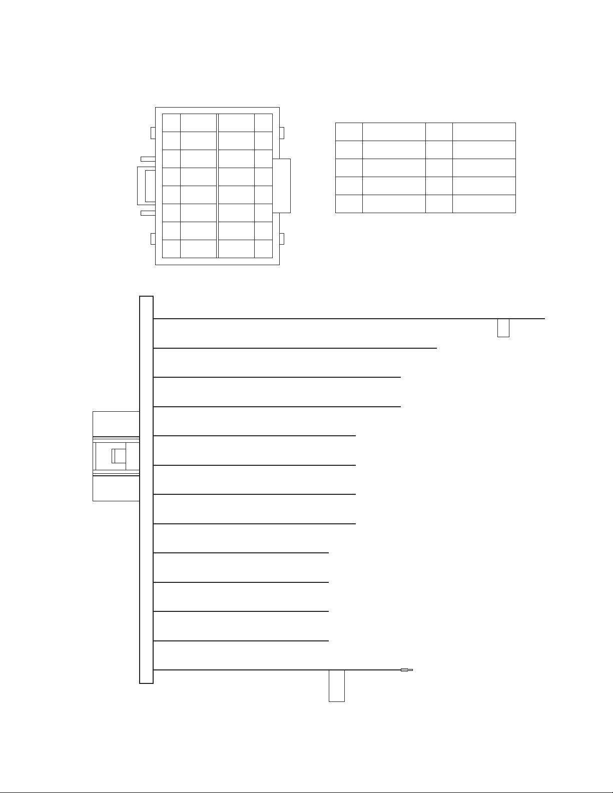
5.1 16 PIN CORD DIAGRAM (for KD-A605, KD-R600,KD-S36)
1
16
15
2
8
GN
GN/BK
7
6
VI/BK
5
VI
4
NC
BL/WH
3
2
RD
1
BK
BK
YL
OR/WH
RD
WH
WH/BK
GY/BK
GY
NC
NC
OR/WH
YL
9
10
11
12
13
14
15
16
BK
RD
BL
WH
VI
Black
Red
Blue
White
Violet
GN
GY
OR
YL
Green
Gray
Orange
Yellow
8
7
5
6
9
10
12
11
3
GN
GN/BK
VI
VI/BK
WH
WH/BK
GY
GY/BK
BL/WH
(No.MA442<Rev.002>)1-25
Page 26
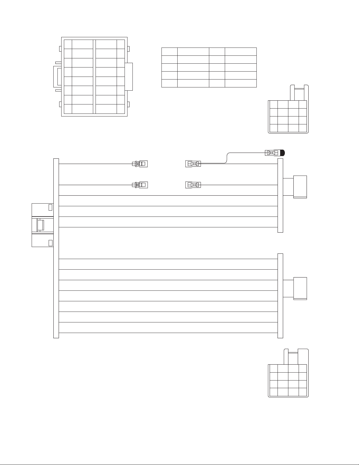
5.2 16 PIN CORD DIAGRAM (for KD-R601)
2
16
15
1
3
13
8
7
6
5
4
3
2
1
RD1
YL1
OR/WH
BK
BL/WH
BR
GN
GN/BK
VI/BK
VI
NC
BL/WH
RD
BK
WH
WH/BK
GY/BK
GY
BR
NC
OR/WH
YL
10
11
12
13
14
15
16
9
Black
BK
RD
BL
WH
VI
Red
Blue
White
Violet
GN
GY Gray
BR
OR
YL
RD2
Green
Brown
Orange
Yellow
1
3
5
7
RD3
YL2
NC
NC
BL/WH
RD3
7
4
6
8
5
2
BR
YL2
OR/WH
BK
2
4
6
8
8
7
5
6
9
10
12
11
GN
GN/BK
VI
VI/BK
WH
WH/BK
GY
GY/BK
7
8
1
2
5
6
3
4
VI/BK
VI
1
GY
3
WH
5
GN
7
GY/BK
WH/BK
GN/BK
2
4
6
8
1-26 (No.MA442<Rev.002>)
Page 27

5.3 16 PIN CORD DIAGRAM (for KD-R604, KD-R605, KD-R606)
1
16
4
3
8
7
6
5
4
3
2
1
BK
YL
BL
BL/WH
GN
GN/BK
VI/BK
VI
BL
BL/WH
RD
BK
WH
WH/BK
GY/BK
GY
NC
NC
OR/WH
YL
9
10
11
12
13
14
15
16
BK
RD
BL
WH
VI
Black
Red
Blue
White
Violet
GN
GY
OR
YL
Green
Gray
Orange
Yellow
RD
2
OR/WH
15
GN
8
GN/BK
7
VI
5
VI/BK
6
WH
9
WH/BK
10
GY
12
GY/BK
11
(No.MA442<Rev.002>)1-27
Page 28

Victor Company of Japan, Limited
Mobile Entertainment Division 10-1,1chome,Ohwatari-machi,Maebashi-city,371-8543,Japan
(No.MA442<Rev.002>)
Printed in Japan
VSE
Page 29

REVISION INFORMATION
CD RECEIVER
KD-A605J, KD-R600J, KD-R601E,
KD-R601EX, KD-R601EY, KD-R601EU,
KD-R604UI, KD-R605U, KD-R605UN,
KD-R605UT, KD-R605UH, KD-R606U,
KD-R606UN, KD-R606UT, KD-R606UH,
KD-S36J
■ OVERVIEW
Add KD-S36J, supported reduction in cost, and board contents were changed.
■ DETAILS
COVER SECTION
Title Line No.MA442<Rev.001> No.MA442<Rev.002> Description
Revision Rev.001 Rev.002
Issue Date 2009/02 2009/08
Model No. KD-A605J, KD-R600J, KD-R601E,
Cover Illustration ILLUSTRATION(ma442_0001.png) ILLUSTRATION(ma442_0001.png)
SPECIFICATION 1 KD-A605/KD-R600 KD-A605/KD-R600/KD-S36
11
13
KD-R601EU, KD-R601EX, KD-R601EY,
KD-R604UI, KD-R605U, KD-R605UH,
KD-R605UN, KD-R605UT, KD-R606U,
KD-R606UH, KD-R606UN, KD-R606UT
KD-R600
2.5 V/20 kΩ load (full scale)
KD-R600
2.5 V/20 kΩ load (full scale)
KD-A605J, KD-R600J, KD-R601E,
KD-R601EU, KD-R601EX, KD-R601EY,
KD-R604UI, KD-R605U, KD-R605UH,
KD-R605UN, KD-R605UT, KD-R606U,
KD-R606UH, KD-R606UN, KD-R606UT,
KD-S36J
KD-R600/KD-S36
2.5 V/20 kΩ load (full scale)
KD-R600/KD-S36
2.5 V/20 kΩ load (full scale)
COPYRIGHT © 2009 Victor Company of Japan, Limited
MA442-R002
2009/08
Page 30

SECTION 2 SPECIFIC SERVICE INSTRUCTIONS
Title Line No.MA442<Rev.001> No.MA442<Rev.002> Description
2 SPECIFIC SERVICE
INSTRUCTIONS
2.1 Identification method T - 2.1 Identification method
1 - Supported reduction in cost, and board contents
2 - ILLUSTRATION(ma442_2001.png)
1 This service manual does not describe
SPECIFIC SERVICE INSTRUCTIONS.
-
was changed.A set put the following label on is an
object.
SECTION 5 TROUBLESHOOTING
Title Line No.MA442<Rev.001> No.MA442<Rev.002> Description
5.1 16 PIN CORD DIAGRAM (for
KD-A605, KD-R600,KD-S36)
T 5.1 16 PIN CORD DIAGRAM (for KD-
A605, KD-R600)
5.1 16 PIN CORD DIAGRAM (for KD-A605,
KD-R600,KD-S36)
STANDARD SCHEMATIC DIAGRAMS
Schematic Diagram
Diagram Name No.MA442<Rev.001> No.MA442<Rev.002> Description
Menu Main section Old Main section
Menu LCD & Key control section Old LCD & Key control sectionion
Menu CD section Old CD section
Menu - Main section
Menu - LCD & Key control section
Menu - CD section
Printed Circuit Board
Diagram Name No.MA442<Rev.001> No.MA442<Rev.002> Description
Menu Main board Old Main board
Menu Switch board Old Switch board
Menu LED board Old LED board
Menu CD board Old CD board
Menu CD switch board Old CD switch board
Menu Photo board Old Photo board
Menu - Main board
Menu - Switch board
Menu - LED board
Menu - CD board
Menu - CD switch board
Menu - Photo board
Description of Major ICs
Diagram Name No.MA442<Rev.001> No.MA442<Rev.002> Description
Menu - IC302: BR24S16F-W-X
Menu - IC681: KSM-2003TN2M
Menu - IC701: MN101E16YFE
Menu - IC701: MN101E16YFF
Menu IC1: TEF6606T/V3-X IC1: TEF6606T/V5-X
2 (MA442-R002)
Page 31

PARTS LIST
r
MODEL No. LIST
Model No. No.MA442<Rev.002>
KD-A605J 01
KD-R600J 02
KD-R601E 03
KD-R601EU 06
KD-R601EX 04
KD-R601EY 05
General assembly [M1MM]
Symbol o
!
M1MM 4 GE33325-002A ------------ INSULATOR (Deletion) 1 01,02,03,04,05,06,07,08,09,0A,0B,
M1MM 4 ------------ GE33325-002A INSULATOR (Addition) 1 01,02,07,08,09,0A,0B,0C,0D,0E,0F
M1MM 4 ------------ GE33325-003A INSULATOR (Addition) 1 03,04,05,06,10
M1MM 17 ------------ GE10215-003A FRONT CHASSIS (Addition) 1 10
M1MM 23 GE33592-001A GE33592-019A FRONT PANEL ASSY 1 01
M1MM 23 GE33592-014A GE33592-028A FRONT PANEL ASSY 1 02,0C,0D,0E,0F,10
M1MM 23 GE33592-003A GE33592-021A FRONT PANEL ASSY 1 03,04,05,06
M1MM 23 GE33592-016A GE33592-029A FRONT PANEL ASSY 1 07,08,09,0A,0B
M1MM 24 ------------ GE33435-047A FINDER ASSY (Addition) 1 10
M1MM 24 GE33435-010A GE33435-026A FINDER ASSY 1 01
M1MM 24 GE33435-006A GE33435-027A FINDER ASSY 1 02
M1MM 24 GE33435-011A GE33435-028A FINDER ASSY 1 03,04,05,06
M1MM 24 GE33435-007A GE33435-029A FINDER ASSY 1 07
M1MM 24 GE33435-008A GE33435-030A FINDER ASSY 1 08,09,0A,0B
M1MM 24 GE33435-009A GE33435-031A FINDER ASSY 1 0C,0D,0E,0F
M1MM 28 GE33416-001A ------------ SRC BUTTON (Deletion) 1 01,02,03,04,05,06,0C,0D,0E,0F
M1MM 28 ------------ GE33416-001A SRC BUTTON (Addition) 1 01,02,0C,0D,0E,0F
M1MM 28 ------------ GE33416-003A SRC BUTTON (Addition) 1 03,04,05,06,10
M1MM 29 GE33417-001A ------------ DISP BUTTON (Deletion) 1 01,02,03,04,05,06,0C,0D,0E,0F
M1MM 29 ------------ GE33417-001A DISP BUTTON (Addition) 1 01,02,0C,0D,0E,0F
M1MM 29 ------------ GE33417-003A DISP BUTTON (Addition) 1 03,04,05,06,10
M1MM 40 GE10252-001A GE10252-002A REAR COVER 1 01,02,03,04,05,06,07,08,09,0A,0B,
M1MM 46 ------------ GE33875-001A NAME PLATE (Addition) 1 10
M1MM 54 ------------ LV45386-001A R2 INDICATION (Addition) 1 01,02,03,04,05,06,07,08,09,0A,0B,
M1MM 55 ------------ GE40225-001A CAR STEREO TAG (Addition) 1 10
M1MM 56 ------------ QYSDSP4014ZA SCREW (Addition) 1 10
M1MM 57 ------------ GE40282-001A LABEL (Addition) 1 10
<Rev.001> <Rev.002>
Part No.
Model No. No.MA442<Rev.002>
KD-R604UI 07
KD-R605U 08
KD-R605UH 0B
KD-R605UN 09
KD-R605UT 0A
KD-R606U 0C
Part Name Description Qty Models
Model No. No.MA442<Rev.002>
KD-R606UH 0F
KD-R606UN 0D
KD-R606UT 0E
KD-S36J 10
0C,0D,0E,0F
0C,0D,0E,0F,10
0C,0D,0E,0F,10
CD mechanism [MBMM]
Symbol or
!
MBMM 3 LV22300-001A LV22300-002A SLIDE CAM (L) 1 01,02,03,04,05,06,07,08,09,0A,
MBMM 10 LV11260-002A LV11260-003A TOP COVER 1 01,02,03,04,05,06,07,08,09,0A,
MBMM 13 LV36903-002A LV36903-003A L M BASE ASSY 1 01,02,03,04,05,06,07,08,09,0A,
MBMM 16 LV36805-001A LV36805-002A M WHEEL GEAR 1 01,02,03,04,05,06,07,08,09,0A,
MBMM 22 LV44589-002A ------------ COMPRESSION
MBMM 39 LV36815-001A LV36815-002A F WHEEL GEAR 1 01,02,03,04,05,06,07,08,09,0A,
MBMM 41 LV44589-002A ------------ COMPRESSION
MBMM 42 LV37326-002A LV37326-003A CLAMPER ASSY 1 01,02,03,04,05,06,07,08,09,0A,
MBMM 48 VKZ4539-054 VKZ4539-054 MINI SCREW 6 > 4 01,02,03,04,05,06,07,08,09,0A,
MBMM 56 LV44559-002A LV44559-003A ROLLER SHAFT 1 01,02,03,04,05,06,07,08,09,0A,
<Rev.001> <Rev.002>
Part No.
Part Name Description Qty Models
0B,0C,0D,0E,0F,10
0B,0C,0D,0E,0F,10
0B,0C,0D,0E,0F,10
SPRING
(Deletion) 1 01,02,03,04,05,06,07,08,09,0A,
(Deletion) 1 01,02,03,04,05,06,07,08,09,0A,
SPRING
0B,0C,0D,0E,0F,10
0B,0C,0D,0E,0F
0B,0C,0D,0E,0F,10
0B,0C,0D,0E,0F
0B,0C,0D,0E,0F,10
0B,0C,0D,0E,0F,10
0B,0C,0D,0E,0F,10
(MA442-R002) 3
Page 32

Symbol or
!
MBMM 57 LV22325-002A LV22744-001A R HOLDER ASSY 2 1 01,02,03,04,05,06,07,08,09,0A,
MBMM 59 LV44590-001A LV44590-001A WASHER 2 > 1 01,02,03,04,05,06,07,08,09,0A,
MBMM 60 LV44561-001A LV45268-001A ROLLER COLLAR 2 1 01,02,03,04,05,06,07,08,09,0A,
MBMM 65 LV34916-001A LV34916-002A WIRE CLAMP 1 01,02,03,04,05,06,07,08,09,0A,
MBMM 66 ------------ LV45269-001A R HOLDER ROD (Addition) 1 01,02,03,04,05,06,07,08,09,0A,
MBMM 67 ------------ LV45270-001A WASHER 2 (Addition) 1 01,02,03,04,05,06,07,08,09,0A,
<Rev.001> <Rev.002>
Part No.
Part Name Description Qty Models
0B,0C,0D,0E,0F,10
0B,0C,0D,0E,0F,10
0B,0C,0D,0E,0F,10
0B,0C,0D,0E,0F,10
0B,0C,0D,0E,0F,10
0B,0C,0D,0E,0F,10
Main board [04]
Symbol or
!
! 04 IC1 ------------ TEF6606T/V5-X IC (Addition) 1 01,02,03,04,05,06,07,08,09,0A,0B,0C,
! 04 IC71 ------------ LC72725KM-X IC (Addition) 1 03,04,05,06
04 IC161 ------------ TDA7718-X IC (Addition) 1 01,02,03,04,05,06,07,08,09,0A,0B,0C,
! 04 IC301 ------------ TDA7851A IC (Addition) 1 01,02,03,04,05,06,07,08,09,0A,0B,0C,
04 IC381 ------------ NJM2160BV-X IC (Addition) 1 01
04 IC401 ------------ TPS2051BD-X IC (Addition) 1 01,02,03,04,05,06,07,08,09,0A,0B,0C,
! 04 IC701 ------------ MN101E16YFE IC (Addition) 1 01,02,07,08,09,0A,0B,0C,0D,0E,0F,10
! 04 IC701 ------------ MN101E16YFF IC (Addition) 1 03,04,05,06
04 IC702 ------------ S-80824CNNB-G-W IC (Addition) 1 01,02,03,04,05,06,07,08,09,0A,0B,0C,
04 IC702 or ------------ IC-PST3424U-X IC (Addition) 1 01,02,03,04,05,06,07,08,09,0A,0B,0C,
04 IC771 ------------ S-24CS04AFJ-G-X IC (Addition) 1 01,02,07,08,09,0A,0B,0C,0D,0E,0F,10
04 IC771 ------------ S-24CS16A0I-G-X IC (Addition) 1 03,04,05,06
04 IC801 ------------ 74AHCT126PW-X IC (Addition) 1 01,02,03,04,05,06,07,08,09,0A,0B,0C,
! 04 IC901 ------------ AN34002A REGULATOR
! 04 IC931 ------------ BD9007HFP-W IC (Addition) 1 01,02,03,04,05,06,07,08,09,0A,0B,0C,
04 Q331 ------------ IMX9-W PAIR
04 Q781 ------------ RT1P141C-X DIGI
04 Q781 or ------------ UN2111-X TRANSISTOR (Addition) 1 01,02,03,04,05,06,07,08,09,0A,0B,0C,
04 Q782 ------------ 2SC1623A/5-6/-X TRANSISTOR (Addition) 1 01,02,03,04,05,06,07,08,09,0A,0B,0C,
04 Q782 or ------------ 2SC3928A/QR/-X TRANSISTOR (Addition) 1 01,02,03,04,05,06,07,08,09,0A,0B,0C,
04 Q784 ------------ RT1P141C-X DIGI
04 Q784 or ------------ UN2111-X TRANSISTOR (Addition) 1 01,02,03,04,05,06,07,08,09,0A,0B,0C,
04 Q881 ------------ RT1N141C-X DIGI
04 Q881 or ------------ UN2211-X TRANSISTOR (Addition) 1 01,02,03,04,05,06,07,08,09,0A,0B,0C,
04 Q891 ------------ RT1N141C-X DIGI
04 Q891 or ------------ UN2211-X TRANSISTOR (Addition) 1 03,04,05,06
04 Q976 ------------ RT1N141C-X DIGI
04 Q976 or ------------ UN2211-X TRANSISTOR (Addition) 1 01,02,03,04,05,06,07,08,09,0A,0B,0C,
04 Q977 ------------ 2SA812A/5-6/-X TRANSISTOR (Addition) 1 01,02,03,04,05,06,07,08,09,0A,0B,0C,
04 Q977 or ------------ ISA1530AC1/QR/X TRANSISTOR (Addition) 1 01,02,03,04,05,06,07,08,09,0A,0B,0C,
<Rev.001> <Rev.002>
Part No.
Part Name Description Qty Models
0D,0E,0F,10
0D,0E,0F,10
0D,0E,0F,10
0D,0E,0F,10
0D,0E,0F,10
0D,0E,0F,10
IC
(Addition) 1 01,02,03,04,05,06,07,08,09,0A,0B,0C,
(Addition) 1 01,02,03,04,05,06,07,08,09,0A,0B,0C,
TRANSISTOR
(Addition) 1 01,02,03,04,05,06,07,08,09,0A,0B,0C,
TRANSISTOR
(Addition) 1 01,02,03,04,05,06,07,08,09,0A,0B,0C,
TRANSISTOR
(Addition) 1 01,02,03,04,05,06,07,08,09,0A,0B,0C,
TRANSISTOR
(Addition) 1 03,04,05,06
TRANSISTOR
(Addition) 1 01,02,03,04,05,06,07,08,09,0A,0B,0C,
TRANSISTOR
0D,0E,0F,10
0D,0E,0F,10
0D,0E,0F,10
0D,0E,0F,10
0D,0E,0F,10
0D,0E,0F,10
0D,0E,0F,10
0D,0E,0F,10
0D,0E,0F,10
0D,0E,0F,10
0D,0E,0F,10
0D,0E,0F,10
0D,0E,0F,10
0D,0E,0F,10
0D,0E,0F,10
0D,0E,0F,10
4 (MA442-R002)
Page 33

Symbol or
!
04 Q978 ------------ 2SC1623A/5-6/-X TRANSISTOR (Addition) 1 01,02,03,04,05,06,07,08,09,0A,0B,0C,
04 Q978 or ------------ 2SC3928A/QR/-X TRANSISTOR (Addition) 1 01,02,03,04,05,06,07,08,09,0A,0B,0C,
04 D331 ------------ MC2836-X DIODE (Addition) 1 01,02,03,04,05,06,07,08,09,0A,0B,0C,
04 D331 or ------------ MA152WA-X DIODE (Addition) 1 01,02,03,04,05,06,07,08,09,0A,0B,0C,
04 D711 ------------ UDZW6.2B-X Z DIODE (Addition) 1 01,03,04,05,06
04 D711 or ------------ MA8062/M/-X Z DIODE (Addition) 1 01,03,04,05,06
04 D712 ------------ 1SS355W-X DIODE (Addition) 1 01,02,03,04,05,06,07,08,09,0A,0B,0C,
04 D712 or ------------ MA111-X SI DIODE (Addition) 1 01,02,03,04,05,06,07,08,09,0A,0B,0C,
04 D715 ------------ UDZW5.1B-X SB DIODE (Addition) 1 01,02,03,04,05,06,07,08,09,0A,0B,0C,
04 D715 or ------------ MA8051/M/-X Z DIODE (Addition) 1 01,02,03,04,05,06,07,08,09,0A,0B,0C,
04 D716 ------------ UDZW5.1B-X SB DIODE (Addition) 1 01,02,03,04,05,06,07,08,09,0A,0B,0C,
04 D716 or ------------ MA8051/M/-X Z DIODE (Addition) 1 01,02,03,04,05,06,07,08,09,0A,0B,0C,
04 D717 ------------ UDZW5.1B-X SB DIODE (Addition) 1 01,02,03,04,05,06,07,08,09,0A,0B,0C,
04 D717 or ------------ MA8051/M/-X Z DIODE (Addition) 1 01,02,03,04,05,06,07,08,09,0A,0B,0C,
04 D718 ------------ UDZW5.1B-X SB DIODE (Addition) 1 01,02,03,04,05,06,07,08,09,0A,0B,0C,
04 D718 or ------------ MA8051/M/-X Z DIODE (Addition) 1 01,02,03,04,05,06,07,08,09,0A,0B,0C,
04 D719 ------------ UDZW5.1B-X SB DIODE (Addition) 1 01,02,03,04,05,06,07,08,09,0A,0B,0C,
04 D719 or ------------ MA8051/M/-X Z DIODE (Addition) 1 01,02,03,04,05,06,07,08,09,0A,0B,0C,
04 D720 ------------ UDZW5.1B-X SB DIODE (Addition) 1 01,02,03,04,05,06,07,08,09,0A,0B,0C,
04 D720 or ------------ MA8051/M/-X Z DIODE (Addition) 1 01,02,03,04,05,06,07,08,09,0A,0B,0C,
04 D781 ------------ 1SS355W-X DIODE (Addition) 1 01,02,03,04,05,06,07,08,09,0A,0B,0C,
04 D781 or ------------ MA111-X SI DIODE (Addition) 1 01,02,03,04,05,06,07,08,09,0A,0B,0C,
04 D784 ------------ UDZW11B-X Z DIODE (Addition) 1 01,02,03,04,05,06,07,08,09,0A,0B,0C,
04 D784 or ------------ MA8110/M/-X Z DIODE (Addition) 1 01,02,03,04,05,06,07,08,09,0A,0B,0C,
04 D785 ------------ 1SS355W-X DIODE (Addition) 1 01,02,03,04,05,06,07,08,09,0A,0B,0C,
04 D785 or ------------ MA111-X SI DIODE (Addition) 1 01,02,03,04,05,06,07,08,09,0A,0B,0C,
04 D851 ------------ MA22F20-X SB DIODE (Addition) 1 07,08,09,0A,0B,0C,0D,0E,0F
04 D852 ------------ MA22D23-X SB DIODE (Addition) 1 07,08,09,0A,0B,0C,0D,0E,0F
04 D852 or ------------ CRS03-W SB DIODE (Addition) 1 07,08,09,0A,0B,0C,0D,0E,0F
04 D891 ------------ MC2836-X DIODE (Addition) 1 03,04,05,06
04 D891 or ------------ MA152WA-X DIODE (Addition) 1 03,04,05,06
04 D901 ------------ 1N5401-F64 SI DIODE (Addition) 1 01,02,03,04,05,06,07,08,09,0A,0B,0C,
04 D901 or ------------ 1N5401-TU-15 SI DIODE (Addition) 1 01,02,03,04,05,06,07,08,09,0A,0B,0C,
04 D902 ------------ GS1J-LTP-X DIODE (Addition) 1 03,04,05,06
04 D931 ------------ RSX201L-30-X SB DIODE (Addition) 1 01,02,07,08,09,0A,0B,0C,0D,0E,0F,10
04 D932 ------------ MA22D23-X SB DIODE (Addition) 1 03,04,05,06
04 D933 ------------ MA22D23-X SB DIODE (Addition) 1 03,04,05,06
04 D971 ------------ MA22F20-X SB DIODE (Addition) 1 01,02,03,04,05,06,07,08,09,0A,0B,0C,
04 D972 ------------ MA22D23-X SB DIODE (Addition) 1 01,02,03,04,05,06,07,08,09,0A,0B,0C,
04 D972 or ------------ CRS03-W SB DIODE (Addition) 1 01,02,03,04,05,06,07,08,09,0A,0B,0C,
<Rev.001> <Rev.002>
Part No.
Part Name Description Qty Models
0D,0E,0F,10
0D,0E,0F,10
0D,0E,0F,10
0D,0E,0F,10
0D,0E,0F,10
0D,0E,0F,10
0D,0E,0F,10
0D,0E,0F,10
0D,0E,0F,10
0D,0E,0F,10
0D,0E,0F,10
0D,0E,0F,10
0D,0E,0F,10
0D,0E,0F,10
0D,0E,0F,10
0D,0E,0F,10
0D,0E,0F,10
0D,0E,0F,10
0D,0E,0F,10
0D,0E,0F,10
0D,0E,0F,10
0D,0E,0F,10
0D,0E,0F,10
0D,0E,0F,10
0D,0E,0F,10
0D,0E,0F,10
0D,0E,0F,10
0D,0E,0F,10
0D,0E,0F,10
(MA442-R002) 5
Page 34

Symbol or
!
04 C1 ------------ NCB31HK-102X C CAPACITOR (Addition) 1 01,02,03,04,05,06,07,08,09,0A,0B,0C,
04 C2 ------------ NDC31HJ-5R6X C CAPACITOR (Addition) 1 01,02,03,04,05,06,07,08,09,0A,0B,0C,
04 C3 ------------ NCB31HK-102X C CAPACITOR (Addition) 1 01,02,03,04,05,06,07,08,09,0A,0B,0C,
04 C4 ------------ NCB31AK-224X C CAPACITOR (Addition) 1 01,02,03,04,05,06,07,08,09,0A,0B,0C,
04 C5 ------------ NDC31HJ-150X C CAPACITOR (Addition) 1 01,02,03,04,05,06,07,08,09,0A,0B,0C,
04 C6 ------------ NDC31HJ-220X C CAPACITOR (Addition) 1 01,02,03,04,05,06,07,08,09,0A,0B,0C,
04 C10 ------------ NCB31AK-105X C CAPACITOR (Addition) 1 01,02,03,04,05,06,07,08,09,0A,0B,0C,
04 C11 ------------ NCB31HK-103X C CAPACITOR (Addition) 1 01,02,03,04,05,06,07,08,09,0A,0B,0C,
04 C12 ------------ NCB31HK-103X C CAPACITOR (Addition) 1 01,02,03,04,05,06,07,08,09,0A,0B,0C,
04 C13 ------------ NCB31AK-105X C CAPACITOR (Addition) 1 01,02,03,04,05,06,07,08,09,0A,0B,0C,
04 C14 ------------ NCB31AK-224X C CAPACITOR (Addition) 1 01,02,03,04,05,06,07,08,09,0A,0B,0C,
04 C15 ------------ NCB31CK-104X C CAPACITOR (Addition) 1 01,02,03,04,05,06,07,08,09,0A,0B,0C,
04 C16 ------------ NCB31HK-103X C CAPACITOR (Addition) 1 01,02,03,04,05,06,07,08,09,0A,0B,0C,
04 C17 ------------ NCB31CK-104X C CAPACITOR (Addition) 1 01,02,03,04,05,06,07,08,09,0A,0B,0C,
04 C18 ------------ NCB31HK-103X C CAPACITOR (Addition) 1 01,02,03,04,05,06,07,08,09,0A,0B,0C,
04 C19 ------------ NCB31CK-104X C CAPACITOR (Addition) 1 01,02,03,04,05,06,07,08,09,0A,0B,0C,
04 C22 ------------ NDC31HJ-150X C CAPACITOR (Addition) 1 01,02,03,04,05,06,07,08,09,0A,0B,0C,
04 C23 ------------ NCB31CK-104X C CAPACITOR (Addition) 1 01,02,03,04,05,06,07,08,09,0A,0B,0C,
04 C24 ------------ NCB31HK-103X C CAPACITOR (Addition) 1 01,02,03,04,05,06,07,08,09,0A,0B,0C,
04 C25 ------------ NCB31HK-103X C CAPACITOR (Addition) 1 01,02,03,04,05,06,07,08,09,0A,0B,0C,
04 C26 ------------ QEKJ1CM-107Z E CAPACITOR (Addition) 1 01,02,03,04,05,06,07,08,09,0A,0B,0C,
04 C32 ------------ NDC31HJ-2R0X C CAPACITOR (Addition) 1 01,02,03,04,05,06,07,08,09,0A,0B,0C,
04 C71 ------------ NDC31HJ-561X C CAPACITOR (Addition) 1 03,04,05,06
04 C72 ------------ NDC31HJ-331X C CAPACITOR (Addition) 1 03,04,05,06
04 C73 ------------ QEKJ1EM-106Z E CAPACITOR (Addition) 1 03,04,05,06
04 C74 ------------ NDC31HJ-330X C CAPACITOR (Addition) 1 03,04,05,06
04 C75 ------------ NDC31HJ-330X C CAPACITOR (Addition) 1 03,04,05,06
04 C76 ------------ NCB31HK-103X C CAPACITOR (Addition) 1 03,04,05,06
04 C78 ------------ NCB31HK-122X C CAPACITOR (Addition) 1 03,04,05,06
04 C161 ------------ NCB31AK-105X C CAPACITOR (Addition) 1 01,02,03,04,05,06,07,08,09,0A,0B,0C,
04 C162 ------------ QEKJ1HM-105Z E CAPACITOR (Addition) 1 01,02,03,04,05,06,07,08,09,0A,0B,0C,
04 C164 ------------ NCB31AK-105X C CAPACITOR (Addition) 1 01,02,03,04,05,06,07,08,09,0A,0B,0C,
04 C165 ------------ NCB31AK-105X C CAPACITOR (Addition) 1 01,02,03,04,05,06,07,08,09,0A,0B,0C,
04 C166 ------------ NDC31HJ-560X C CAPACITOR (Addition) 1 01,02,03,04,05,06,07,08,09,0A,0B,0C,
04 C171 ------------ NCB31AK-105X C CAPACITOR (Addition) 1 01,02,03,04,05,06,07,08,09,0A,0B,0C,
04 C172 ------------ QEKJ1HM-105Z E CAPACITOR (Addition) 1 01,02,03,04,05,06,07,08,09,0A,0B,0C,
04 C174 ------------ NCB31AK-105X C CAPACITOR (Addition) 1 01,02,03,04,05,06,07,08,09,0A,0B,0C,
04 C176 ------------ NDC31HJ-560X C CAPACITOR (Addition) 1 01,02,03,04,05,06,07,08,09,0A,0B,0C,
<Rev.001> <Rev.002>
Part No.
Part Name Description Qty Models
0D,0E,0F,10
0D,0E,0F,10
0D,0E,0F,10
0D,0E,0F,10
0D,0E,0F,10
0D,0E,0F,10
0D,0E,0F,10
0D,0E,0F,10
0D,0E,0F,10
0D,0E,0F,10
0D,0E,0F,10
0D,0E,0F,10
0D,0E,0F,10
0D,0E,0F,10
0D,0E,0F,10
0D,0E,0F,10
0D,0E,0F,10
0D,0E,0F,10
0D,0E,0F,10
0D,0E,0F,10
0D,0E,0F,10
0D,0E,0F,10
0D,0E,0F,10
0D,0E,0F,10
0D,0E,0F,10
0D,0E,0F,10
0D,0E,0F,10
0D,0E,0F,10
0D,0E,0F,10
0D,0E,0F,10
0D,0E,0F,10
6 (MA442-R002)
Page 35

Symbol or
!
04 C177 ------------ NDC31HJ-560X C CAPACITOR (Addition) 1 01,02,03,04,05,06,07,08,09,0A,0B,0C,
04 C178 ------------ QTE1C57-106Z E CAPACITOR (Addition) 1 01,02,03,04,05,06,07,08,09,0A,0B,0C,
04 C183 ------------ QEKJ1AM-227Z E CAPACITOR (Addition) 1 01,02,03,04,05,06,07,08,09,0A,0B,0C,
04 C184 ------------ NCB31AK-105X C CAPACITOR (Addition) 1 01,02,03,04,05,06,07,08,09,0A,0B,0C,
04 C301 ------------ QFV91HJ-474Z MF
04 C302 ------------ QFV91HJ-474Z MF
04 C311 ------------ QFV91HJ-474Z MF
04 C312 ------------ QFV91HJ-474Z MF
04 C315 ------------ NCB31AK-105X C CAPACITOR (Addition) 1 01,02,03,04,05,06,07,08,09,0A,0B,0C,
04 C316 ------------ QEKJ1HM-475Z E CAPACITOR (Addition) 1 01,02,03,04,05,06,07,08,09,0A,0B,0C,
04 C317 ------------ QTE1C57-476Z E CAPACITOR (Addition) 1 01,02,03,04,05,06,07,08,09,0A,0B,0C,
04 C318 ------------ NCB21AK-225X-A C CAPACITOR (Addition) 1 01,02,03,04,05,06,07,08,09,0A,0B,0C,
04 C319 ------------ NCB31EK-223X C CAPACITOR (Addition) 1 01,02,03,04,05,06,07,08,09,0A,0B,0C,
04 C320 ------------ NCB31EK-223X C CAPACITOR (Addition) 1 01,02,03,04,05,06,07,08,09,0A,0B,0C,
04 C322 ------------ NCB31HK-103X C CAPACITOR (Addition) 1 01,02,03,04,05,06,07,08,09,0A,0B,0C,
04 C323 ------------ NCB31HK-103X C CAPACITOR (Addition) 1 01,02,03,04,05,06,07,08,09,0A,0B,0C,
04 C324 ------------ NCB31HK-103X C CAPACITOR (Addition) 1 01,02,03,04,05,06,07,08,09,0A,0B,0C,
04 C326 ------------ QEKJ1CM-226Z E CAPACITOR (Addition) 1 01,02,03,04,05,06,07,08,09,0A,0B,0C,
04 C340 ------------ NDC31HJ-820X C CAPACITOR (Addition) 1 01,02,03,04,05,06,07,08,09,0A,0B,0C,
04 C345 ------------ NDC31HJ-560X C CAPACITOR (Addition) 1 01,02,03,04,05,06,07,08,09,0A,0B,0C,
04 C346 ------------ NDC31HJ-560X C CAPACITOR (Addition) 1 01,02,03,04,05,06,07,08,09,0A,0B,0C,
04 C347 ------------ NDC31HJ-560X C CAPACITOR (Addition) 1 01,02,03,04,05,06,07,08,09,0A,0B,0C,
04 C348 ------------ NDC31HJ-560X C CAPACITOR (Addition) 1 01,02,03,04,05,06,07,08,09,0A,0B,0C,
04 C381 ------------ QEKJ1HM-475Z E CAPACITOR (Addition) 1 01,02,03,04,05,06,07,08,09,0A,0B,0C,
04 C382 ------------ QEKJ1HM-475Z E CAPACITOR (Addition) 1 01,02,03,04,05,06,07,08,09,0A,0B,0C,
04 C383 ------------ QEKJ1HM-475Z E CAPACITOR (Addition) 1 01
04 C384 ------------ QEKJ1HM-475Z E CAPACITOR (Addition) 1 01
04 C385 ------------ NCB31EK-104X C CAPACITOR (Addition) 1 01
04 C386 ------------ NCB31EK-104X C CAPACITOR (Addition) 1 01
04 C387 ------------ NCB31HK-152X C CAPACITOR (Addition) 1 01
04 C388 ------------ NCB31HK-152X C CAPACITOR (Addition) 1 01
04 C389 ------------ QEKJ1CM-107Z E CAPACITOR (Addition) 1 01
04 C390 ------------ QEKJ1CM-107Z E CAPACITOR (Addition) 1 01
04 C392 ------------ QEKJ1CM-106Z E CAPACITOR (Addition) 1 01
04 C401 ------------ NDC31HJ-820X C CAPACITOR (Addition) 1 01,02,03,04,05,06,07,08,09,0A,0B,0C,
04 C402 ------------ NDC31HJ-101X C CAPACITOR (Addition) 1 01,02,07,08,09,0A,0B,0C,0D,0E,0F,10
04 C418 ------------ NDC31HJ-270X C CAPACITOR (Addition) 1 01,02,03,04,05,06,07,08,09,0A,0B,0C,
04 C419 ------------ NDC31HJ-270X C CAPACITOR (Addition) 1 01,02,03,04,05,06,07,08,09,0A,0B,0C,
04 C583 ------------ NCB31HK-332X C CAPACITOR (Addition) 1 01,02,03,04,05,06,07,08,09,0A,0B,0C,
04 C584 ------------ NCB31HK-332X C CAPACITOR (Addition) 1 01,02,03,04,05,06,07,08,09,0A,0B,0C,
<Rev.001> <Rev.002>
Part No.
Part Name Description Qty Models
0D,0E,0F,10
0D,0E,0F,10
0D,0E,0F,10
CAPACITOR
(Addition) 1 01,02,03,04,05,06,07,08,09,0A,0B,0C,
(Addition) 1 01,02,03,04,05,06,07,08,09,0A,0B,0C,
CAPACITOR
(Addition) 1 01,02,03,04,05,06,07,08,09,0A,0B,0C,
CAPACITOR
(Addition) 1 01,02,03,04,05,06,07,08,09,0A,0B,0C,
CAPACITOR
0D,0E,0F,10
0D,0E,0F,10
0D,0E,0F,10
0D,0E,0F,10
0D,0E,0F,10
0D,0E,0F,10
0D,0E,0F,10
0D,0E,0F,10
0D,0E,0F,10
0D,0E,0F,10
0D,0E,0F,10
0D,0E,0F,10
0D,0E,0F,10
0D,0E,0F,10
0D,0E,0F,10
0D,0E,0F,10
0D,0E,0F,10
0D,0E,0F,10
0D,0E,0F,10
0D,0E,0F,10
0D,0E,0F,10
0D,0E,0F,10
0D,0E,0F,10
0D,0E,0F,10
0D,0E,0F,10
0D,0E,0F,10
0D,0E,0F,10
(MA442-R002) 7
Page 36

Symbol or
!
04 C585 ------------ QTE1H64-225Z E CAPACITOR (Addition) 1 01,02,03,04,05,06,07,08,09,0A,0B,0C,
04 C586 ------------ QTE1H64-225Z E CAPACITOR (Addition) 1 01,02,03,04,05,06,07,08,09,0A,0B,0C,
04 C587 ------------ NDC31HJ-331X C CAPACITOR (Addition) 1 01,02,03,04,05,06,07,08,09,0A,0B,0C,
04 C588 ------------ NDC31HJ-331X C CAPACITOR (Addition) 1 01,02,03,04,05,06,07,08,09,0A,0B,0C,
04 C703 ------------ NDC31HJ-200X C CAPACITOR (Addition) 1 01,02,03,04,05,06,07,08,09,0A,0B,0C,
04 C704 ------------ NDC31HJ-200X C CAPACITOR (Addition) 1 01,02,03,04,05,06,07,08,09,0A,0B,0C,
04 C706 ------------ NDC31HJ-821X C CAPACITOR (Addition) 1 01,02,03,04,05,06,07,08,09,0A,0B,0C,
04 C707 ------------ QEKJ1CM-107Z E CAPACITOR (Addition) 1 01,02,03,04,05,06,07,08,09,0A,0B,0C,
04 C708 ------------ NCB31CK-104X C CAPACITOR (Addition) 1 01,02,03,04,05,06,07,08,09,0A,0B,0C,
04 C709 ------------ NCB31CK-104X C CAPACITOR (Addition) 1 01,02,03,04,05,06,07,08,09,0A,0B,0C,
04 C710 ------------ NDC31HJ-101X C CAPACITOR (Addition) 1 01,03,04,05,06
04 C711 ------------ QEKJ0JM-476Z E CAPACITOR (Addition) 1 01,02,03,04,05,06,07,08,09,0A,0B,0C,
04 C714 ------------ NCB31CK-104X C CAPACITOR (Addition) 1 01,02,03,04,05,06,07,08,09,0A,0B,0C,
04 C715 ------------ NCB31CK-104X C CAPACITOR (Addition) 1 01,02,03,04,05,06,07,08,09,0A,0B,0C,
04 C717 ------------ NDC31HJ-821X C CAPACITOR (Addition) 1 01,02,03,04,05,06,07,08,09,0A,0B,0C,
04 C718 ------------ NCB31CK-104X C CAPACITOR (Addition) 1 01,02,03,04,05,06,07,08,09,0A,0B,0C,
04 C719 ------------ QERF1AM-107Z E CAPACITOR (Addition) 1 01,02,03,04,05,06,07,08,09,0A,0B,0C,
04 C720 ------------ NDC31HJ-820X C CAPACITOR (Addition) 1 01,02,03,04,05,06,07,08,09,0A,0B,0C,
04 C721 ------------ NCB31CK-104X C CAPACITOR (Addition) 1 01,02,03,04,05,06,07,08,09,0A,0B,0C,
04 C722 ------------ QERF1EM-475Z E CAPACITOR (Addition) 1 01,02,03,04,05,06,07,08,09,0A,0B,0C,
04 C728 ------------ NCB31AK-105X C CAPACITOR (Addition) 1 01,02,03,04,05,06,07,08,09,0A,0B,0C,
04 C729 ------------ NCB31HK-392X C CAPACITOR (Addition) 1 01,02,03,04,05,06,07,08,09,0A,0B,0C,
04 C730 ------------ NCB31HK-392X C CAPACITOR (Addition) 1 01,02,03,04,05,06,07,08,09,0A,0B,0C,
04 C732 ------------ NCB31HK-122X C CAPACITOR (Addition) 1 01,02,03,04,05,06,07,08,09,0A,0B,0C,
04 C734 ------------ NDC31HJ-560X C CAPACITOR (Addition) 1 01,02,03,04,05,06,07,08,09,0A,0B,0C,
04 C735 ------------ NDC31HJ-560X C CAPACITOR (Addition) 1 01,02,03,04,05,06,07,08,09,0A,0B,0C,
04 C742 ------------ NDC31HJ-560X C CAPACITOR (Addition) 1 03,04,05,06
04 C771 ------------ NCB31CK-473X C CAPACITOR (Addition) 1 01,02,03,04,05,06,07,08,09,0A,0B,0C,
04 C781 ------------ QEKJ0JM-107Z E CAPACITOR (Addition) 1 01,02,03,04,05,06,07,08,09,0A,0B,0C,
04 C784 ------------ QEKJ1CM-107Z E CAPACITOR (Addition) 1 01,02,03,04,05,06,07,08,09,0A,0B,0C,
04 C801 ------------ NCB31CK-473X C CAPACITOR (Addition) 1 01,02,03,04,05,06,07,08,09,0A,0B,0C,
04 C851 ------------ QEKJ1EM-106Z E CAPACITOR (Addition) 1 07,08,09,0A,0B,0C,0D,0E,0F
04 C852 ------------ NCB31CK-224X C CAPACITOR (Addition) 1 07,08,09,0A,0B,0C,0D,0E,0F
04 C881 ------------ QERF1CM-226Z E CAPACITOR (Addition) 1 01,02,03,04,05,06,07,08,09,0A,0B,0C,
04 C891 ------------ NCB31CK-104X C CAPACITOR (Addition) 1 03,04,05,06
04 C901 ------------ QEZ0870-278 E CAPACITOR (Addition) 1 01,02,03,04,05,06,07,08,09,0A,0B,0C,
04 C903 ------------ QEKJ1CM-476Z E CAPACITOR (Addition) 1 01,02,03,04,05,06,07,08,09,0A,0B,0C,
04 C905 ------------ QEKJ1CM-476Z E CAPACITOR (Addition) 1 01,02,03,04,05,06,07,08,09,0A,0B,0C,
<Rev.001> <Rev.002>
Part No.
Part Name Description Qty Models
0D,0E,0F,10
0D,0E,0F,10
0D,0E,0F,10
0D,0E,0F,10
0D,0E,0F,10
0D,0E,0F,10
0D,0E,0F,10
0D,0E,0F,10
0D,0E,0F,10
0D,0E,0F,10
0D,0E,0F,10
0D,0E,0F,10
0D,0E,0F,10
0D,0E,0F,10
0D,0E,0F,10
0D,0E,0F,10
0D,0E,0F,10
0D,0E,0F,10
0D,0E,0F,10
0D,0E,0F,10
0D,0E,0F,10
0D,0E,0F,10
0D,0E,0F,10
0D,0E,0F,10
0D,0E,0F,10
0D,0E,0F,10
0D,0E,0F,10
0D,0E,0F,10
0D,0E,0F,10
0D,0E,0F,10
0D,0E,0F,10
0D,0E,0F,10
0D,0E,0F,10
8 (MA442-R002)
Page 37

Symbol or
!
04 C906 ------------ NCB31HK-103X C CAPACITOR (Addition) 1 01,02,03,04,05,06,07,08,09,0A,0B,0C,
04 C907 ------------ QEKJ1AM-107Z E CAPACITOR (Addition) 1 01,02,03,04,05,06,07,08,09,0A,0B,0C,
04 C908 ------------ QEKJ1EM-475Z E CAPACITOR (Addition) 1 01,02,03,04,05,06,07,08,09,0A,0B,0C,
04 C909 ------------ QEKJ0JM-227Z E CAPACITOR (Addition) 1 01,02,03,04,05,06,10
04 C909 ------------ QERF0JM-337Z E CAPACITOR (Addition) 1 07,08,09,0A,0B,0C,0D,0E,0F
04 C910 ------------ QEKJ1EM-106Z E CAPACITOR (Addition) 1 01,02,03,04,05,06,07,08,09,0A,0B,0C,
04 C912 ------------ NCB31HK-103X C CAPACITOR (Addition) 1 01,02,03,04,05,06,07,08,09,0A,0B,0C,
04 C913 ------------ QEKJ1EM-106Z E CAPACITOR (Addition) 1 01,02,03,04,05,06,07,08,09,0A,0B,0C,
04 C916 ------------ NCB31HK-103X C CAPACITOR (Addition) 1 01,02,03,04,05,06,07,08,09,0A,0B,0C,
04 C918 ------------ NCB31HK-104X C CAPACITOR (Addition) 1 01,02,03,04,05,06,07,08,09,0A,0B,0C,
04 C928 ------------ NCB31HK-472X C CAPACITOR (Addition) 1 01,02,03,04,05,06,07,08,09,0A,0B,0C,
04 C931 ------------ QEZ0595-477Z E CAPACITOR (Addition) 1 01,02,07,08,09,0A,0B,0C,0D,0E,0F,10
04 C931 ------------ QETN1VM-477Z-S E CAPACITOR (Addition) 1 03,04,05,06
04 C932 ------------ QBZ0006-337Z TA E
04 C933 ------------ NCB31HK-152X C CAPACITOR (Addition) 1 01,02,03,04,05,06,07,08,09,0A,0B,0C,
04 C937 ------------ NCB31AK-105X C CAPACITOR (Addition) 1 01,02,03,04,05,06,07,08,09,0A,0B,0C,
04 C938 ------------ NCJ21EK-225X-D C CAPACITOR (Addition) 1 01,02,03,04,05,06,07,08,09,0A,0B,0C,
04 C940 ------------ NDC31HJ-180X C CAPACITOR (Addition) 1 01,02,03,04,05,06,07,08,09,0A,0B,0C,
04 C971 ------------ NCB31EK-104X C CAPACITOR (Addition) 1 01,02,03,04,05,06,07,08,09,0A,0B,0C,
04 C992 ------------ NDC31HJ-220X C CAPACITOR (Addition) 1 01,02,03,04,05,06,07,08,09,0A,0B,0C,
04 R2 ------------ NRSA63J-824X MG RESISTOR (Addition) 1 01,02,03,04,05,06,07,08,09,0A,0B,0C,
04 R4 ------------ NRSA63J-472X MG RESISTOR (Addition) 1 01,02,03,04,05,06,07,08,09,0A,0B,0C,
04 R5 ------------ NRS181J-220X MG RESISTOR (Addition) 1 01,02,03,04,05,06,07,08,09,0A,0B,0C,
04 R6 ------------ NRSA63J-101X MG RESISTOR (Addition) 1 01,02,03,04,05,06,07,08,09,0A,0B,0C,
04 R7 ------------ NRSA63J-101X MG RESISTOR (Addition) 1 01,02,03,04,05,06,07,08,09,0A,0B,0C,
04 R10 ------------ NRSA63J-0R0X MG RESISTOR (Addition) 1 01,02,03,04,05,06,07,08,09,0A,0B,0C,
04 R11 ------------ NRS181J-4R7X MG RESISTOR (Addition) 1 01,02,03,04,05,06,07,08,09,0A,0B,0C,
04 R12 ------------ NRZ0084-0R0X MG RESISTOR (Addition) 1 03,04,05,06
04 R14 ------------ NRSA63J-472X MG RESISTOR (Addition) 1 01,02,03,04,05,06,07,08,09,0A,0B,0C,
04 R15 ------------ NRSA63J-472X MG RESISTOR (Addition) 1 01,02,03,04,05,06,07,08,09,0A,0B,0C,
04 R71 ------------ NRSA63J-0R0X MG RESISTOR (Addition) 1 03,04,05,06
04 R72 ------------ NRSA63J-222X MG RESISTOR (Addition) 1 03,04,05,06
04 R73 ------------ NRSA63J-222X MG RESISTOR (Addition) 1 03,04,05,06
04 R74 ------------ NRSA02J-101X MG RESISTOR (Addition) 1 03,04,05,06
04 R81 ------------ NRSA63J-153X MG RESISTOR (Addition) 1 01,02,10
04 R81 ------------ NRSA63J-682X MG RESISTOR (Addition) 1 03,04,05,06,07,08,09,0A,0B,0C,0D,0E,
04 R82 ------------ NRSA63J-822X MG RESISTOR (Addition) 1 01,02,10
04 R82 ------------ NRSA63J-682X MG RESISTOR (Addition) 1 03,04,05,06,07,08,09,0A,0B,0C,0D,0E,
04 R91 ------------ NRSA63J-153X MG RESISTOR (Addition) 1 01,02,10
04 R91 ------------ NRSA63J-682X MG RESISTOR (Addition) 1 03,04,05,06,07,08,09,0A,0B,0C,0D,0E,
04 R92 ------------ NRSA63J-822X MG RESISTOR (Addition) 1 01,02,10
<Rev.001> <Rev.002>
Part No.
Part Name Description Qty Models
0D,0E,0F,10
0D,0E,0F,10
0D,0E,0F,10
0D,0E,0F,10
0D,0E,0F,10
0D,0E,0F,10
0D,0E,0F,10
0D,0E,0F,10
0D,0E,0F,10
CAPACITOR
(Addition) 1 01,02,03,04,05,06,07,08,09,0A,0B,0C,
0D,0E,0F,10
0D,0E,0F,10
0D,0E,0F,10
0D,0E,0F,10
0D,0E,0F,10
0D,0E,0F,10
0D,0E,0F,10
0D,0E,0F,10
0D,0E,0F,10
0D,0E,0F,10
0D,0E,0F,10
0D,0E,0F,10
0D,0E,0F,10
0D,0E,0F,10
0D,0E,0F,10
0D,0E,0F,10
0F
0F
0F
(MA442-R002) 9
Page 38

Symbol or
!
04 R92 ------------ NRSA63J-682X MG RESISTOR (Addition) 1 03,04,05,06,07,08,09,0A,0B,0C,0D,0E,
04 R161 ------------ NRSA63J-472X MG RESISTOR (Addition) 1 01,02,03,04,05,06,07,08,09,0A,0B,0C,
04 R162 ------------ NRSA63J-472X MG RESISTOR (Addition) 1 01,02,03,04,05,06,07,08,09,0A,0B,0C,
04 R171 ------------ NRSA63J-101X MG RESISTOR (Addition) 1 01,02,03,04,05,06,07,08,09,0A,0B,0C,
04 R172 ------------ NRSA63J-101X MG RESISTOR (Addition) 1 01,02,03,04,05,06,07,08,09,0A,0B,0C,
04 R305 ------------ NRSA63J-102X MG RESISTOR (Addition) 1 01,02,03,04,05,06,07,08,09,0A,0B,0C,
04 R309 ------------ NRS181J-100X MG RESISTOR (Addition) 1 01,02,03,04,05,06,07,08,09,0A,0B,0C,
04 R310 ------------ NRSA63J-472X MG RESISTOR (Addition) 1 01,02,03,04,05,06,07,08,09,0A,0B,0C,
04 R341 ------------ NRSA63J-222X MG RESISTOR (Addition) 1 01,02,03,04,05,06,07,08,09,0A,0B,0C,
04 R342 ------------ NRSA63J-821X MG RESISTOR (Addition) 1 01,02,03,04,05,06,07,08,09,0A,0B,0C,
04 R343 ------------ NRSA02J-101X MG RESISTOR (Addition) 1 01,02,03,04,05,06,07,08,09,0A,0B,0C,
04 R344 ------------ NRSA63J-473X MG RESISTOR (Addition) 1 01,02,03,04,05,06,07,08,09,0A,0B,0C,
04 R351 ------------ NRSA63J-222X MG RESISTOR (Addition) 1 01,02,03,04,05,06,07,08,09,0A,0B,0C,
04 R352 ------------ NRSA63J-821X MG RESISTOR (Addition) 1 01,02,03,04,05,06,07,08,09,0A,0B,0C,
04 R353 ------------ NRSA02J-101X MG RESISTOR (Addition) 1 01,02,03,04,05,06,07,08,09,0A,0B,0C,
04 R354 ------------ NRSA63J-473X MG RESISTOR (Addition) 1 01,02,03,04,05,06,07,08,09,0A,0B,0C,
04 R381 ------------ NRSA63J-102X MG RESISTOR (Addition) 1 01
04 R382 ------------ NRSA63J-102X MG RESISTOR (Addition) 1 01
04 R383 ------------ NRSA63J-104X MG RESISTOR (Addition) 1 01
04 R384 ------------ NRSA63J-104X MG RESISTOR (Addition) 1 01
04 R385 ------------ NRSA63J-223X MG RESISTOR (Addition) 1 01
04 R386 ------------ NRSA63J-223X MG RESISTOR (Addition) 1 01
04 R387 ------------ NRSA63J-333X MG RESISTOR (Addition) 1 01
04 R388 ------------ NRSA63J-333X MG RESISTOR (Addition) 1 01
04 R389 ------------ NRSA63J-0R0X MG RESISTOR (Addition) 1 02,03,04,05,06,07,08,09,0A,0B,0C,0D,
04 R390 ------------ NRSA63J-0R0X MG RESISTOR (Addition) 1 02,03,04,05,06,07,08,09,0A,0B,0C,0D,
04 R583 ------------ NRSA63J-153X MG RESISTOR (Addition) 1 01,02,03,04,05,06,07,08,09,0A,0B,0C,
04 R584 ------------ NRSA63J-153X MG RESISTOR (Addition) 1 01,02,03,04,05,06,07,08,09,0A,0B,0C,
04 R585 ------------ NRSA63J-102X MG RESISTOR (Addition) 1 01,02,03,04,05,06,07,08,09,0A,0B,0C,
04 R586 ------------ NRSA63J-102X MG RESISTOR (Addition) 1 01,02,03,04,05,06,07,08,09,0A,0B,0C,
04 R587 ------------ NRSA63J-183X MG RESISTOR (Addition) 1 01,02,03,04,05,06,07,08,09,0A,0B,0C,
04 R588 ------------ NRSA63J-183X MG RESISTOR (Addition) 1 01,02,03,04,05,06,07,08,09,0A,0B,0C,
04 R701 ------------ NRSA63J-103X MG RESISTOR (Addition) 1 01,02,03,04,05,06,07,08,09,0A,0B,0C,
04 R702 ------------ NRSA63J-103X MG RESISTOR (Addition) 1 01,02,03,04,05,06,07,08,09,0A,0B,0C,
04 R703 ------------ NRSA63J-104X MG RESISTOR (Addition) 1 01,02,03,04,05,06,07,08,09,0A,0B,0C,
04 R704 ------------ NRSA63J-104X MG RESISTOR (Addition) 1 01,02,03,04,05,06,07,08,09,0A,0B,0C,
04 R708 ------------ NRSA63J-104X MG RESISTOR (Addition) 1 01,02,10
04 R709 ------------ NRSA63J-473X MG RESISTOR (Addition) 1 03,04,05,06,07,08,09,0A,0B,0C,0D,0E,
04 R711 ------------ NRSA63J-473X MG RESISTOR (Addition) 1 01,02,03,04,05,06,07,08,09,0A,0B,0C,
<Rev.001> <Rev.002>
Part No.
Part Name Description Qty Models
0F
0D,0E,0F,10
0D,0E,0F,10
0D,0E,0F,10
0D,0E,0F,10
0D,0E,0F,10
0D,0E,0F,10
0D,0E,0F,10
0D,0E,0F,10
0D,0E,0F,10
0D,0E,0F,10
0D,0E,0F,10
0D,0E,0F,10
0D,0E,0F,10
0D,0E,0F,10
0D,0E,0F,10
0E,0F,10
0E,0F,10
0D,0E,0F,10
0D,0E,0F,10
0D,0E,0F,10
0D,0E,0F,10
0D,0E,0F,10
0D,0E,0F,10
0D,0E,0F,10
0D,0E,0F,10
0D,0E,0F,10
0D,0E,0F,10
0F
0D,0E,0F,10
10 (MA442-R002)
Page 39

Symbol or
!
04 R712 ------------ NRSA63J-331X MG RESISTOR (Addition) 1 01,02,03,04,05,06,07,08,09,0A,0B,0C,
04 R714 ------------ NRSA63J-0R0X MG RESISTOR (Addition) 1 01,02,03,04,05,06,07,08,09,0A,0B,0C,
04 R717 ------------ NRSA63J-102X MG RESISTOR (Addition) 1 01,02,03,04,05,06,07,08,09,0A,0B,0C,
04 R718 ------------ NRSA63J-102X MG RESISTOR (Addition) 1 01,02,03,04,05,06,07,08,09,0A,0B,0C,
04 R719 ------------ NRSA63J-102X MG RESISTOR (Addition) 1 01,02,03,04,05,06,07,08,09,0A,0B,0C,
04 R720 ------------ NRSA63J-102X MG RESISTOR (Addition) 1 01,02,03,04,05,06,07,08,09,0A,0B,0C,
04 R721 ------------ NRSA63J-102X MG RESISTOR (Addition) 1 01,02,03,04,05,06,07,08,09,0A,0B,0C,
04 R722 ------------ NRS181J-102X MG RESISTOR (Addition) 1 01,02,03,04,05,06,07,08,09,0A,0B,0C,
04 R723 ------------ NRSA63J-102X MG RESISTOR (Addition) 1 01,02,03,04,05,06,07,08,09,0A,0B,0C,
04 R724 ------------ NRSA63J-102X MG RESISTOR (Addition) 1 01,02,03,04,05,06,07,08,09,0A,0B,0C,
04 R725 ------------ NRSA63J-102X MG RESISTOR (Addition) 1 01,02,03,04,05,06,07,08,09,0A,0B,0C,
04 R726 ------------ NRSA63J-273X MG RESISTOR (Addition) 1 01,02,03,04,05,06,07,08,09,0A,0B,0C,
04 R727 ------------ NRSA63J-122X MG RESISTOR (Addition) 1 01,02,03,04,05,06,07,08,09,0A,0B,0C,
04 R728 ------------ NRSA63J-102X MG RESISTOR (Addition) 1 01,02,03,04,05,06,07,08,09,0A,0B,0C,
04 R730 ------------ NRSA63J-102X MG RESISTOR (Addition) 1 01,02,03,04,05,06,07,08,09,0A,0B,0C,
04 R731 ------------ NRSA63J-101X MG RESISTOR (Addition) 1 01,02,03,04,05,06,07,08,09,0A,0B,0C,
04 R732 ------------ NRSA63J-473X MG RESISTOR (Addition) 1 01,02,03,04,05,06,07,08,09,0A,0B,0C,
04 R733 ------------ NRSA63J-473X MG RESISTOR (Addition) 1 01,02,03,04,05,06,07,08,09,0A,0B,0C,
04 R734 ------------ NRSA63J-471X MG RESISTOR (Addition) 1 01,02,03,04,05,06,07,08,09,0A,0B,0C,
04 R736 ------------ NRSA63J-561X MG RESISTOR (Addition) 1 01,02,03,04,05,06,07,08,09,0A,0B,0C,
04 R737 ------------ NRSA63J-561X MG RESISTOR (Addition) 1 01,02,03,04,05,06,07,08,09,0A,0B,0C,
04 R738 ------------ NRSA63J-561X MG RESISTOR (Addition) 1 01,02,03,04,05,06,07,08,09,0A,0B,0C,
04 R739 ------------ NRSA63J-101X MG RESISTOR (Addition) 1 01,02,03,04,05,06,07,08,09,0A,0B,0C,
04 R740 ------------ NRSA63J-561X MG RESISTOR (Addition) 1 01,02,03,04,05,06,07,08,09,0A,0B,0C,
04 R741 ------------ NRSA63J-101X MG RESISTOR (Addition) 1 01,02,03,04,05,06,07,08,09,0A,0B,0C,
04 R742 ------------ NRSA63J-101X MG RESISTOR (Addition) 1 01,02,03,04,05,06,07,08,09,0A,0B,0C,
04 R743 ------------ NRSA63J-101X MG RESISTOR (Addition) 1 03,04,05,06
04 R744 ------------ NRSA63J-101X MG RESISTOR (Addition) 1 01,02,03,04,05,06,07,08,09,0A,0B,0C,
04 R745 ------------ NRSA63J-271X MG RESISTOR (Addition) 1 03,04,05,06
04 R746 ------------ NRSA63J-104X MG RESISTOR (Addition) 1 01,02,03,04,05,06,07,08,09,0A,0B,0C,
04 R747 ------------ NRSA63J-103X MG RESISTOR (Addition) 1 01,02,03,04,05,06,07,08,09,0A,0B,0C,
04 R748 ------------ NRSA63J-122X MG RESISTOR (Addition) 1 01,02,03,04,05,06,07,08,09,0A,0B,0C,
04 R749 ------------ NRSA63J-102X MG RESISTOR (Addition) 1 01,02,03,04,05,06,07,08,09,0A,0B,0C,
04 R750 ------------ NRS181J-104X MG RESISTOR (Addition) 1 01,02,03,04,05,06,07,08,09,0A,0B,0C,
04 R752 ------------ NRSA63J-472X MG RESISTOR (Addition) 1 01,02,03,04,05,06,07,08,09,0A,0B,0C,
04 R753 ------------ NRSA63J-472X MG RESISTOR (Addition) 1 01,02,03,04,05,06,07,08,09,0A,0B,0C,
<Rev.001> <Rev.002>
Part No.
Part Name Description Qty Models
0D,0E,0F,10
0D,0E,0F,10
0D,0E,0F,10
0D,0E,0F,10
0D,0E,0F,10
0D,0E,0F,10
0D,0E,0F,10
0D,0E,0F,10
0D,0E,0F,10
0D,0E,0F,10
0D,0E,0F,10
0D,0E,0F,10
0D,0E,0F,10
0D,0E,0F,10
0D,0E,0F,10
0D,0E,0F,10
0D,0E,0F,10
0D,0E,0F,10
0D,0E,0F,10
0D,0E,0F,10
0D,0E,0F,10
0D,0E,0F,10
0D,0E,0F,10
0D,0E,0F,10
0D,0E,0F,10
0D,0E,0F,10
0D,0E,0F,10
0D,0E,0F,10
0D,0E,0F,10
0D,0E,0F,10
0D,0E,0F,10
0D,0E,0F,10
0D,0E,0F,10
0D,0E,0F,10
(MA442-R002) 11
Page 40
Symbol or
!
04 R755 ------------ NRSA63J-472X MG RESISTOR (Addition) 1 01,02,03,04,05,06,07,08,09,0A,0B,0C,
04 R756 ------------ NRSA63J-472X MG RESISTOR (Addition) 1 01,02,03,04,05,06,07,08,09,0A,0B,0C,
04 R757 ------------ NRSA63J-122X MG RESISTOR (Addition) 1 01,02,03,04,05,06,07,08,09,0A,0B,0C,
04 R758 ------------ NRSA63J-473X MG RESISTOR (Addition) 1 01,02,03,04,05,06,07,08,09,0A,0B,0C,
04 R760 ------------ NRSA63J-122X MG RESISTOR (Addition) 1 01,02,03,04,05,06,07,08,09,0A,0B,0C,
04 R761 ------------ NRSA63J-122X MG RESISTOR (Addition) 1 01,02,03,04,05,06,07,08,09,0A,0B,0C,
04 R762 ------------ NRSA63J-122X MG RESISTOR (Addition) 1 01,02,03,04,05,06,07,08,09,0A,0B,0C,
04 R763 ------------ NRSA63J-823X MG RESISTOR (Addition) 1 01,02,03,04,05,06,07,08,09,0A,0B,0C,
04 R764 ------------ NRSA63J-823X MG RESISTOR (Addition) 1 01,02,03,04,05,06,07,08,09,0A,0B,0C,
04 R765 ------------ NRSA63J-472X MG RESISTOR (Addition) 1 01,02,03,04,05,06,07,08,09,0A,0B,0C,
04 R766 ------------ NRS181J-472X MG RESISTOR (Addition) 1 01,02,03,04,05,06,07,08,09,0A,0B,0C,
04 R767 ------------ NRSA63J-473X MG RESISTOR (Addition) 1 01,02,03,04,05,06,07,08,09,0A,0B,0C,
04 R768 ------------ NRSA63J-472X MG RESISTOR (Addition) 1 01,02,03,04,05,06,07,08,09,0A,0B,0C,
04 R770 ------------ NRSA63J-222X MG RESISTOR (Addition) 1 01,02,03,04,05,06,10
04 R771 ------------ NRSA63J-271X MG RESISTOR (Addition) 1 01,02,03,04,05,06,07,08,09,0A,0B,0C,
04 R772 ------------ NRSA63J-271X MG RESISTOR (Addition) 1 01,02,03,04,05,06,07,08,09,0A,0B,0C,
04 R773 ------------ NRSA63J-223X MG RESISTOR (Addition) 1 01,02,03,04,05,06,10
04 R774 ------------ NRSA63J-473X MG RESISTOR (Addition) 1 01,02,03,04,05,06,07,08,09,0A,0B,0C,
04 R775 ------------ NRSA63J-222X MG RESISTOR (Addition) 1 01,02,03,04,05,06,07,08,09,0A,0B,0C,
04 R777 ------------ NRSA63J-103X MG RESISTOR (Addition) 1 01,02,03,04,05,06,07,08,09,0A,0B,0C,
04 R779 ------------ NRSA63J-101X MG RESISTOR (Addition) 1 01,02,03,04,05,06,07,08,09,0A,0B,0C,
04 R781 ------------ NRSA63J-473X MG RESISTOR (Addition) 1 01,02,03,04,05,06,07,08,09,0A,0B,0C,
04 R782 ------------ NRSA63J-472X MG RESISTOR (Addition) 1 01,02,03,04,05,06,07,08,09,0A,0B,0C,
04 R783 ------------ NRSA63J-103X MG RESISTOR (Addition) 1 01,02,03,04,05,06,07,08,09,0A,0B,0C,
04 R784 ------------ NRSA63J-0R0X MG RESISTOR (Addition) 1 01,02,03,04,05,06,07,08,09,0A,0B,0C,
04 R801 ------------ NRSA63J-102X MG RESISTOR (Addition) 1 01,02,03,04,05,06,07,08,09,0A,0B,0C,
04 R802 ------------ NRSA63J-104X MG RESISTOR (Addition) 1 01,02,03,04,05,06,07,08,09,0A,0B,0C,
04 R803 ------------ NRSA63J-682X MG RESISTOR (Addition) 1 01,02,03,04,05,06,07,08,09,0A,0B,0C,
04 R804 ------------ NRSA63J-392X MG RESISTOR (Addition) 1 01,02,03,04,05,06,07,08,09,0A,0B,0C,
04 R805 ------------ NRS181J-0R0X MG RESISTOR (Addition) 1 01,02,03,04,05,06,07,08,09,0A,0B,0C,
04 R806 ------------ NRS181J-102X MG RESISTOR (Addition) 1 01,02,03,04,05,06,07,08,09,0A,0B,0C,
04 R807 ------------ NRSA63J-104X MG RESISTOR (Addition) 1 01,02,03,04,05,06,07,08,09,0A,0B,0C,
04 R808 ------------ NRSA63J-101X MG RESISTOR (Addition) 1 01,02,03,04,05,06,07,08,09,0A,0B,0C,
04 R809 ------------ NRSA63J-473X MG RESISTOR (Addition) 1 01,02,03,04,05,06,07,08,09,0A,0B,0C,
04 R810 ------------ NRSA63J-392X MG RESISTOR (Addition) 1 01,02,03,04,05,06,07,08,09,0A,0B,0C,
04 R811 ------------ NRSA63J-682X MG RESISTOR (Addition) 1 01,02,03,04,05,06,07,08,09,0A,0B,0C,
<Rev.001> <Rev.002>
Part No.
Part Name Description Qty Models
0D,0E,0F,10
0D,0E,0F,10
0D,0E,0F,10
0D,0E,0F,10
0D,0E,0F,10
0D,0E,0F,10
0D,0E,0F,10
0D,0E,0F,10
0D,0E,0F,10
0D,0E,0F,10
0D,0E,0F,10
0D,0E,0F,10
0D,0E,0F,10
0D,0E,0F,10
0D,0E,0F,10
0D,0E,0F,10
0D,0E,0F,10
0D,0E,0F,10
0D,0E,0F,10
0D,0E,0F,10
0D,0E,0F,10
0D,0E,0F,10
0D,0E,0F,10
0D,0E,0F,10
0D,0E,0F,10
0D,0E,0F,10
0D,0E,0F,10
0D,0E,0F,10
0D,0E,0F,10
0D,0E,0F,10
0D,0E,0F,10
0D,0E,0F,10
0D,0E,0F,10
0D,0E,0F,10
12 (MA442-R002)
Page 41

Symbol or
!
04 R812 ------------ NRSA63J-104X MG RESISTOR (Addition) 1 01,02,03,04,05,06,07,08,09,0A,0B,0C,
04 R813 ------------ NRSA63J-102X MG RESISTOR (Addition) 1 01,02,03,04,05,06,07,08,09,0A,0B,0C,
04 R814 ------------ NRSA63J-101X MG RESISTOR (Addition) 1 01,02,03,04,05,06,07,08,09,0A,0B,0C,
04 R819 ------------ NRSA63J-473X MG RESISTOR (Addition) 1 01,02,03,04,05,06,07,08,09,0A,0B,0C,
04 R851 ------------ NRSA63J-103X MG RESISTOR (Addition) 1 07,08,09,0A,0B,0C,0D,0E,0F
04 R881 ------------ NRSA63J-473X MG RESISTOR (Addition) 1 01,02,03,04,05,06,07,08,09,0A,0B,0C,
04 R882 ------------ NRSA63J-472X MG RESISTOR (Addition) 1 01,02,03,04,05,06,07,08,09,0A,0B,0C,
04 R891 ------------ NRSA63J-102X MG RESISTOR (Addition) 1 03,04,05,06
04 R892 ------------ NRSA63J-473X MG RESISTOR (Addition) 1 03,04,05,06
04 R901 ------------ QRE141J-103Y C RESISTOR (Addition) 1 01,02,03,04,05,06,07,08,09,0A,0B,0C,
04 R902 ------------ NRS181J-0R0X MG RESISTOR (Addition) 1 01,02,03,04,05,06,07,08,09,0A,0B,0C,
04 R903 ------------ NRSA02J-472X MG RESISTOR (Addition) 1 01,02,03,04,05,06,07,08,09,0A,0B,0C,
04 R928 ------------ NRSA63J-753X MG RESISTOR (Addition) 1 01,02,03,04,05,06,07,08,09,0A,0B,0C,
04 R929 ------------ NRSA63J-513X MG RESISTOR (Addition) 1 01,02,03,04,05,06,07,08,09,0A,0B,0C,
04 R930 ------------ NRSA63J-0R0X MG RESISTOR (Addition) 1 01,02,03,04,05,06,07,08,09,0A,0B,0C,
04 R937 ------------ NRS181J-221X MG RESISTOR (Addition) 1 01,02,03,04,05,06,07,08,09,0A,0B,0C,
04 R939 ------------ NRS181J-153X MG RESISTOR (Addition) 1 01,02,03,04,05,06,07,08,09,0A,0B,0C,
04 R940 ------------ NRSA63J-823X MG RESISTOR (Addition) 1 01,02,03,04,05,06,07,08,09,0A,0B,0C,
04 R971 ------------ NRS181J-332X MG RESISTOR (Addition) 1 01,02,03,04,05,06,07,08,09,0A,0B,0C,
04 R976 ------------ NRSA02J-273X MG RESISTOR (Addition) 1 01,02,03,04,05,06,07,08,09,0A,0B,0C,
04 R977 ------------ NRSA02J-123X MG RESISTOR (Addition) 1 01,02,03,04,05,06,07,08,09,0A,0B,0C,
04 L1 ------------ NQL093K-R47X COIL (Addition) 1 01,02,03,04,05,06,07,08,09,0A,0B,0C,
04 L2 ------------ NQL093K-1R8X COIL (Addition) 1 01,02,03,04,05,06,07,08,09,0A,0B,0C,
04 L3 ------------ QQL213M-R22Z COIL (Addition) 1 01,02,03,04,05,06,07,08,09,0A,0B,0C,
04 L4 ------------ QQR1813-001 COIL (Addition) 1 01,02,03,04,05,06,07,08,09,0A,0B,0C,
04 L5 ------------ QQL244J-561Z COIL (Addition) 1 01,02,03,04,05,06,07,08,09,0A,0B,0C,
04 L6 ------------ QQL244J-561Z COIL (Addition) 1 01,02,03,04,05,06,07,08,09,0A,0B,0C,
04 L8 ------------ QQL244K-4R7Z COIL (Addition) 1 01,02,03,04,05,06,07,08,09,0A,0B,0C,
04 L161 ------------ NQL553J-27NX COIL (Addition) 1 01,02,03,04,05,06,07,08,09,0A,0B,0C,
04 L701 ------------ QQL244K-4R7Z COIL (Addition) 1 01,02,03,04,05,06,07,08,09,0A,0B,0C,
04 L702 ------------ QQL244K-4R7Z COIL (Addition) 1 01,02,03,04,05,06,07,08,09,0A,0B,0C,
! 04 L901 ------------ QQR1852-001 CHOKE COIL (Addition) 1 01,02,03,04,05,06,07,08,09,0A,0B,0C,
! 04 L901 or ------------ QQR0703-001 CHOKE COIL (Addition) 1 01,02,03,04,05,06,07,08,09,0A,0B,0C,
04 L931 ------------ QQL92AK-330Z COIL (Addition) 1 01,02,03,04,05,06,07,08,09,0A,0B,0C,
04 L932 ------------ NQR0007-002X FERRITE
04 L933 ------------ NQLH25M-4R7X COIL (Addition) 1 01,02,03,04,05,06,07,08,09,0A,0B,0C,
04 CN501 ------------ QGB2027ME-28 CONNECTOR (Addition) 1 01,02,03,04,05,06,07,08,09,0A,0B,0C,
<Rev.001> <Rev.002>
Part No.
Part Name Description Qty Models
0D,0E,0F,10
0D,0E,0F,10
0D,0E,0F,10
0D,0E,0F,10
0D,0E,0F,10
0D,0E,0F,10
0D,0E,0F,10
0D,0E,0F,10
0D,0E,0F,10
0D,0E,0F,10
0D,0E,0F,10
0D,0E,0F,10
0D,0E,0F,10
0D,0E,0F,10
0D,0E,0F,10
0D,0E,0F,10
0D,0E,0F,10
0D,0E,0F,10
0D,0E,0F,10
0D,0E,0F,10
0D,0E,0F,10
0D,0E,0F,10
0D,0E,0F,10
0D,0E,0F,10
0D,0E,0F,10
0D,0E,0F,10
0D,0E,0F,10
0D,0E,0F,10
0D,0E,0F,10
0D,0E,0F,10
BEADS
(Addition) 1 01,02,03,04,05,06,07,08,09,0A,0B,0C,
0D,0E,0F,10
0D,0E,0F,10
0D,0E,0F,10
0D,0E,0F,10
(MA442-R002) 13
Page 42

Symbol or
!
04 CN701 ------------ QGZ1101J1-24 CONNECTOR (Addition) 1 01,02,03,04,05,06,07,08,09,0A,0B,0C,
04 CN703 ------------ QNS0283-001 STEERING
04 CN901 ------------ QNZ0607-001 CAR
04 J1 ------------ QNB0190-001 ANT
04 J321 ------------ QNN0832-001 PIN JACK (Addition) 1 01
04 J321 ------------ QNN0802-001 PIN JACK (Addition) 1 02,03,04,05,06,07,08,09,0A,0B,0C,0D,
04 J801 ------------ QNZ0095-001 CONNECTOR (Addition) 1 01,02,03,04,05,06,07,08,09,0A,0B,0C,
04 S701 ------------ QSW0648-001Z TACT SWITCH (Addition) 1 01,02,03,04,05,06,07,08,09,0A,0B,0C,
04 X1 ------------ QAX0928-001Z CRYSTAL (Addition) 1 01,02,03,04,05,06,07,08,09,0A,0B,0C,
04 X71 ------------ QAX0926-001Z CRYSTAL (Addition) 1 03,04,05,06
04 X701 ------------ QAX0667-001Z C RESONATOR (Addition) 1 01,02,03,04,05,06,07,08,09,0A,0B,0C,
04 X702 ------------ QAX0401-001 CRYSTAL (Addition) 1 01,02,03,04,05,06,07,08,09,0A,0B,0C,
<Rev.001> <Rev.002>
Part No.
Part Name Description Qty Models
REMOTE
(Addition) 1 01,03,04,05,06
(Addition) 1 01,02,03,04,05,06,07,08,09,0A,0B,0C,
CONNECTOR
(Addition) 1 01,02,03,04,05,06,07,08,09,0A,0B,0C,
TERMINAL
0D,0E,0F,10
0D,0E,0F,10
0D,0E,0F,10
0E,0F,10
0D,0E,0F,10
0D,0E,0F,10
0D,0E,0F,10
0D,0E,0F,10
0D,0E,0F,10
Switch board [05]
Symbol or
!
05 IC601 ------------ NCP5623DTBR2G-X IC (Addition) 1 01,02,03,04,05,06,07,08,09,0A,0B,
05 IC661 ------------ PTC6526LQ-L IC (Addition) 1 01,02,03,04,05,06,07,08,09,0A,0B,
05 IC681 ------------ KSM-2003TN2M REMOCON RCV (Addition) 1 10
05 IC681 ------------ NJL29H380A REMOCON RCV (Addition) 1 01,02,03,04,05,06,07,08,09,0A,0B,
05 Q601 ------------ 2SC1623A/5-6/-X TRANSISTOR (Addition) 1 01,02,03,04,05,06,07,08,09,0A,0B,
05 Q601 or ------------ 2SC3928A/QR/-X TRANSISTOR (Addition) 1 01,02,03,04,05,06,07,08,09,0A,0B,
05 Q602 ------------ UNR9211G-X TRANSISTOR (Addition) 1 01,02,03,04,05,06,07,08,09,0A,0B,
05 Q602 or ------------ DTC114EEB-X TRANSISTOR (Addition) 1 01,02,03,04,05,06,07,08,09,0A,0B,
05 Q604 ------------ 2SA2174G-X TRANSISTOR (Addition) 1 01,02,03,04,05,06,07,08,09,0A,0B,
05 Q604 or ------------ 2SA1774/QR/-X TRANSISTOR (Addition) 1 01,02,03,04,05,06,07,08,09,0A,0B,
05 Q605 ------------ UN2222-X IC (Addition) 1 01,02,03,04,05,06,07,08,09,0A,0B,
05 Q605 or ------------ DTD143EK-X TRANSISTOR (Addition) 1 01,02,03,04,05,06,07,08,09,0A,0B,
05 Q607 ------------ 2SA2174G-X TRANSISTOR (Addition) 1 01,02,03,04,05,06,07,08,09,0A,0B,
05 Q607 or ------------ 2SA1774/QR/-X TRANSISTOR (Addition) 1 01,02,03,04,05,06,07,08,09,0A,0B,
05 Q608 ------------ UN2222-X IC (Addition) 1 01,02,03,04,05,06,07,08,09,0A,0B,
05 Q608 or ------------ DTD143EK-X TRANSISTOR (Addition) 1 01,02,03,04,05,06,07,08,09,0A,0B,
05 Q610 ------------ 2SA2174G-X TRANSISTOR (Addition) 1 01,02,03,04,05,06,07,08,09,0A,0B,
05 Q610 or ------------ 2SA1774/QR/-X TRANSISTOR (Addition) 1 01,02,03,04,05,06,07,08,09,0A,0B,
05 Q611 ------------ UN2222-X IC (Addition) 1 01,02,03,04,05,06,07,08,09,0A,0B,
05 Q611 or ------------ DTD143EK-X TRANSISTOR (Addition) 1 01,02,03,04,05,06,07,08,09,0A,0B,
05 D601 ------------ NSSM065T-X LED (Addition) 1 01,02,03,04,05,06,07,08,09,0A,0B,
05 D603 ------------ NSSM065T-X LED (Addition) 1 01,02,03,04,05,06,07,08,09,0A,0B,
<Rev.001> <Rev.002>
Part No.
Part Name Description Qty Models
0C,0D,0E,0F,10
0C,0D,0E,0F,10
0C,0D,0E,0F
0C,0D,0E,0F,10
0C,0D,0E,0F,10
0C,0D,0E,0F,10
0C,0D,0E,0F,10
0C,0D,0E,0F,10
0C,0D,0E,0F,10
0C,0D,0E,0F,10
0C,0D,0E,0F,10
0C,0D,0E,0F,10
0C,0D,0E,0F,10
0C,0D,0E,0F,10
0C,0D,0E,0F,10
0C,0D,0E,0F,10
0C,0D,0E,0F,10
0C,0D,0E,0F,10
0C,0D,0E,0F,10
0C,0D,0E,0F,10
0C,0D,0E,0F,10
14 (MA442-R002)
Page 43

Symbol or
!
05 D604 ------------ NSSM065T-X LED (Addition) 1 01,02,03,04,05,06,07,08,09,0A,0B,
05 D605 ------------ NSSM065T-X LED (Addition) 1 01,02,03,04,05,06,07,08,09,0A,0B,
05 D616 ------------ UDZW5.1B-X SB DIODE (Addition) 1 01,02,03,04,05,06,07,08,09,0A,0B,
05 D616 or ------------ MA8051/M/-X Z DIODE (Addition) 1 01,02,03,04,05,06,07,08,09,0A,0B,
05 D617 ------------ UDZW5.1B-X SB DIODE (Addition) 1 01,02,03,04,05,06,07,08,09,0A,0B,
05 D617 or ------------ MA8051/M/-X Z DIODE (Addition) 1 01,02,03,04,05,06,07,08,09,0A,0B,
05 D630 ------------ LHQ974/LM/-X LED (Addition) 1 01,02,03,04,05,06,07,08,09,0A,0B,
05 D631 ------------ LHQ974/LM/-X LED (Addition) 1 01,02,03,04,05,06,07,08,09,0A,0B,
05 D632 ------------ LHQ974/LM/-X LED (Addition) 1 01,02,03,04,05,06,07,08,09,0A,0B,
05 D650 ------------ MA8056/M/-X Z DIODE (Addition) 1 01,02,03,04,05,06,07,08,09,0A,0B,
05 D650 or ------------ UDZW5.6B-X Z DIODE (Addition) 1 01,02,03,04,05,06,07,08,09,0A,0B,
05 D661 ------------ MA111-X SI DIODE (Addition) 1 01,02,03,04,05,06,07,08,09,0A,0B,
05 D661 or ------------ 1SS355W-X DIODE (Addition) 1 01,02,03,04,05,06,07,08,09,0A,0B,
05 C604 ------------ NCB31CK-105X C CAPACITOR (Addition) 1 01,02,03,04,05,06,07,08,09,0A,0B,
05 C650 ------------ NCB31CK-104X C CAPACITOR (Addition) 1 01,02,03,04,05,06,07,08,09,0A,0B,
05 C651 ------------ NBE21CM-106X TA E
05 C655 ------------ NCJ11EK-106X-R C CAPACITOR (Addition) 1 01,02,03,04,05,06,07,08,09,0A,0B,
05 C661 ------------ NCB31CK-105X C CAPACITOR (Addition) 1 01,02,03,04,05,06,07,08,09,0A,0B,
05 C662 ------------ NDC31HJ-151X C CAPACITOR (Addition) 1 01,02,03,04,05,06,07,08,09,0A,0B,
05 C663 ------------ NCB31CK-223X C CAPACITOR (Addition) 1 01,02,03,04,05,06,07,08,09,0A,0B,
05 C665 ------------ NCB31CK-104X C CAPACITOR (Addition) 1 01,02,03,04,05,06,07,08,09,0A,0B,
05 C666 ------------ NCB31CK-104X C CAPACITOR (Addition) 1 01,02,03,04,05,06,07,08,09,0A,0B,
05 C682 ------------ NCB31EK-104X C CAPACITOR (Addition) 1 01,02,03,04,05,06,07,08,09,0A,0B,
05 C684 ------------ NCB31HK-472X C CAPACITOR (Addition) 1 01,02,03,04,05,06,07,08,09,0A,0B,
05 C685 ------------ NCB31HK-472X C CAPACITOR (Addition) 1 01,02,03,04,05,06,07,08,09,0A,0B,
05 R601 ------------ NRSA63J-821X MG RESISTOR (Addition) 1 01,02,03,04,05,06,07,08,09,0A,0B,
05 R602 ------------ NRSA63J-821X MG RESISTOR (Addition) 1 01,02,03,04,05,06,07,08,09,0A,0B,
05 R603 ------------ NRSA63J-122X MG RESISTOR (Addition) 1 01,02,03,04,05,06,07,08,09,0A,0B,
05 R604 ------------ NRSA63J-182X MG RESISTOR (Addition) 1 01,02,03,04,05,06,07,08,09,0A,0B,
05 R605 ------------ NRSA63J-272X MG RESISTOR (Addition) 1 01,02,03,04,05,06,07,08,09,0A,0B,
05 R606 ------------ NRSA63J-392X MG RESISTOR (Addition) 1 01,02,03,04,05,06,07,08,09,0A,0B,
05 R607 ------------ NRSA63J-392X MG RESISTOR (Addition) 1 01,02,03,04,05,06,07,08,09,0A,0B,
05 R608 ------------ NRSA63J-821X MG RESISTOR (Addition) 1 01,02,03,04,05,06,07,08,09,0A,0B,
05 R609 ------------ NRSA63J-821X MG RESISTOR (Addition) 1 01,02,03,04,05,06,07,08,09,0A,0B,
05 R610 ------------ NRSA63J-122X MG RESISTOR (Addition) 1 01,02,03,04,05,06,07,08,09,0A,0B,
<Rev.001> <Rev.002>
Part No.
Part Name Description Qty Models
0C,0D,0E,0F,10
0C,0D,0E,0F,10
0C,0D,0E,0F,10
0C,0D,0E,0F,10
0C,0D,0E,0F,10
0C,0D,0E,0F,10
0C,0D,0E,0F,10
0C,0D,0E,0F,10
0C,0D,0E,0F,10
0C,0D,0E,0F,10
0C,0D,0E,0F,10
0C,0D,0E,0F,10
0C,0D,0E,0F,10
0C,0D,0E,0F,10
CAPACITOR
(Addition) 1 01,02,03,04,05,06,07,08,09,0A,0B,
0C,0D,0E,0F,10
0C,0D,0E,0F,10
0C,0D,0E,0F,10
0C,0D,0E,0F,10
0C,0D,0E,0F,10
0C,0D,0E,0F,10
0C,0D,0E,0F,10
0C,0D,0E,0F,10
0C,0D,0E,0F,10
0C,0D,0E,0F,10
0C,0D,0E,0F,10
0C,0D,0E,0F,10
0C,0D,0E,0F,10
0C,0D,0E,0F,10
0C,0D,0E,0F,10
0C,0D,0E,0F,10
0C,0D,0E,0F,10
0C,0D,0E,0F,10
0C,0D,0E,0F,10
0C,0D,0E,0F,10
0C,0D,0E,0F,10
(MA442-R002) 15
Page 44

Symbol or
!
05 R611 ------------ NRSA63J-182X MG RESISTOR (Addition) 1 01,02,03,04,05,06,07,08,09,0A,0B,
05 R612 ------------ NRSA63J-272X MG RESISTOR (Addition) 1 01,02,03,04,05,06,07,08,09,0A,0B,
05 R613 ------------ NRSA63J-103X MG RESISTOR (Addition) 1 01,02,03,04,05,06,07,08,09,0A,0B,
05 R614 ------------ NRSA63F-154X MG RESISTOR (Addition) 1 01,02,03,04,05,06,07,08,09,0A,0B,
05 R615 ------------ NRSA63J-101X MG RESISTOR (Addition) 1 01,02,03,04,05,06,07,08,09,0A,0B,
05 R618 ------------ NRSA63J-101X MG RESISTOR (Addition) 1 01,02,03,04,05,06,07,08,09,0A,0B,
05 R626 ------------ NRSA63J-0R0X MG RESISTOR (Addition) 1 01,02,03,04,05,06,07,08,09,0A,0B,
05 R630 ------------ NRSA63J-271X MG RESISTOR (Addition) 1 01,02,03,04,05,06,07,08,09,0A,0B,
05 R631 ------------ NRS181J-471X MG RESISTOR (Addition) 1 01,02,03,04,05,06,07,08,09,0A,0B,
05 R634 ------------ NRSA63J-681X MG RESISTOR (Addition) 1 01,02,03,04,05,06,07,08,09,0A,0B,
05 R636 ------------ NRSA63J-222X MG RESISTOR (Addition) 1 01,02,03,04,05,06,07,08,09,0A,0B,
05 R637 ------------ NRSA63J-222X MG RESISTOR (Addition) 1 01,02,03,04,05,06,07,08,09,0A,0B,
05 R638 ------------ NRSA63J-222X MG RESISTOR (Addition) 1 01,02,03,04,05,06,07,08,09,0A,0B,
05 R644 ------------ NRSA63J-122X MG RESISTOR (Addition) 1 01,02,03,04,05,06,07,08,09,0A,0B,
05 R645 ------------ NRSA63J-122X MG RESISTOR (Addition) 1 01,02,03,04,05,06,07,08,09,0A,0B,
05 R646 ------------ NRSA63J-162X MG RESISTOR (Addition) 1 01,02,03,04,05,06,07,08,09,0A,0B,
05 R647 ------------ NRSA63J-911X MG RESISTOR (Addition) 1 01,02,03,04,05,06,07,08,09,0A,0B,
05 R648 ------------ NRSA63J-911X MG RESISTOR (Addition) 1 01,02,03,04,05,06,07,08,09,0A,0B,
05 R649 ------------ NRSA63J-122X MG RESISTOR (Addition) 1 01,02,03,04,05,06,07,08,09,0A,0B,
05 R651 ------------ NRSA63J-102X MG RESISTOR (Addition) 1 01,02,03,04,05,06,07,08,09,0A,0B,
05 R652 ------------ NRSA63J-0R0X MG RESISTOR (Addition) 1 01,02,03,04,05,06,07,08,09,0A,0B,
05 R656 ------------ NRS181J-331X MG RESISTOR (Addition) 1 01,02,03,04,05,06,07,08,09,0A,0B,
05 R657 ------------ NRS181J-331X MG RESISTOR (Addition) 1 01,02,03,04,05,06,07,08,09,0A,0B,
05 R658 ------------ NRS181J-621X MG RESISTOR (Addition) 1 01,02,03,04,05,06,07,08,09,0A,0B,
05 R660 ------------ NRSA63J-394X MG RESISTOR (Addition) 1 01,02,03,04,05,06,07,08,09,0A,0B,
05 R661 ------------ NRSA63J-102X MG RESISTOR (Addition) 1 01,02,03,04,05,06,07,08,09,0A,0B,
05 R662 ------------ NRSA63J-102X MG RESISTOR (Addition) 1 01,02,03,04,05,06,07,08,09,0A,0B,
05 R663 ------------ NRSA63J-102X MG RESISTOR (Addition) 1 01,02,03,04,05,06,07,08,09,0A,0B,
05 R664 ------------ NRSA63J-224X MG RESISTOR (Addition) 1 01,02,03,04,05,06,07,08,09,0A,0B,
05 R665 ------------ NRSA63J-101X MG RESISTOR (Addition) 1 01,02,03,04,05,06,07,08,09,0A,0B,
05 R666 ------------ NRSA63J-101X MG RESISTOR (Addition) 1 01,02,03,04,05,06,07,08,09,0A,0B,
05 R667 ------------ NRSA63J-101X MG RESISTOR (Addition) 1 01,02,03,04,05,06,07,08,09,0A,0B,
05 R670 ------------ NRSA63J-103X MG RESISTOR (Addition) 1 01,02,03,04,05,06,07,08,09,0A,0B,
05 R671 ------------ NRSA63J-103X MG RESISTOR (Addition) 1 01,02,03,04,05,06,07,08,09,0A,0B,
05 R672 ------------ NRSA63J-101X MG RESISTOR (Addition) 1 01,02,03,04,05,06,07,08,09,0A,0B,
<Rev.001> <Rev.002>
Part No.
Part Name Description Qty Models
0C,0D,0E,0F,10
0C,0D,0E,0F,10
0C,0D,0E,0F,10
0C,0D,0E,0F,10
0C,0D,0E,0F,10
0C,0D,0E,0F,10
0C,0D,0E,0F,10
0C,0D,0E,0F,10
0C,0D,0E,0F,10
0C,0D,0E,0F,10
0C,0D,0E,0F,10
0C,0D,0E,0F,10
0C,0D,0E,0F,10
0C,0D,0E,0F,10
0C,0D,0E,0F,10
0C,0D,0E,0F,10
0C,0D,0E,0F,10
0C,0D,0E,0F,10
0C,0D,0E,0F,10
0C,0D,0E,0F,10
0C,0D,0E,0F,10
0C,0D,0E,0F,10
0C,0D,0E,0F,10
0C,0D,0E,0F,10
0C,0D,0E,0F,10
0C,0D,0E,0F,10
0C,0D,0E,0F,10
0C,0D,0E,0F,10
0C,0D,0E,0F,10
0C,0D,0E,0F,10
0C,0D,0E,0F,10
0C,0D,0E,0F,10
0C,0D,0E,0F,10
0C,0D,0E,0F,10
0C,0D,0E,0F,10
16 (MA442-R002)
Page 45

Symbol or
!
!
05 R673 ------------ NRSA63J-101X MG RESISTOR (Addition) 1 01,02,03,04,05,06,07,08,09,0A,0B,
05 R681 ------------ NRSA63J-471X MG RESISTOR (Addition) 1 01,02,03,04,05,06,07,08,09,0A,0B,
05 R682 ------------ NRSA63J-102X MG RESISTOR (Addition) 1 01,02,03,04,05,06,07,08,09,0A,0B,
05 R6043 ------------ NRSA63J-0R0X MG RESISTOR (Addition) 1 01,02,03,04,05,06,07,08,09,0A,0B,
05 R6044 ------------ NRSA63J-0R0X MG RESISTOR (Addition) 1 01,02,03,04,05,06,07,08,09,0A,0B,
05 L602 ------------ NQR0536-001X CHOKE COIL (Addition) 1 01,02,03,04,05,06,07,08,09,0A,0B,
05 CJ601 ------------ QGZ1101K1-24 CONNECTOR (Addition) 1 01,02,03,04,05,06,07,08,09,0A,0B,
05 CN603 ------------ QNZ1006-001 USB JACK (Addition) 1 01,02,03,04,05,06,07,08,09,0A,0B,
05 J601 ------------ QNS0280-001 3.5 JACK (Addition) 1 10
05 J601 ------------ QNS0215-001 3.5 JACK (Addition) 1 01,02,03,04,05,06,07,08,09,0A,0B,
05 JS686 ------------ QSW1263-001 ROTARY
05 K670 ------------ NQR0007-002X FERRITE
05 K670 ------------ NRSA02J-0R0X MG RESISTOR (Addition) 1 03,04,05,06
05 K671 ------------ NQR0007-002X FERRITE
05 K671 ------------ NRSA02J-0R0X MG RESISTOR (Addition) 1 03,04,05,06
05 K672 ------------ NQR0007-002X FERRITE
05 K672 ------------ NRSA02J-0R0X MG RESISTOR (Addition) 1 03,04,05,06
05 K673 ------------ NRSA02J-0R0X MG RESISTOR (Addition) 1 01,02,03,04,05,06,07,08,09,0A,0B,
05 S601 ------------ NSW0124-001X TACT SW (Addition) 1 01,02,03,04,05,06,07,08,09,0A,0B,
05 S602 ------------ NSW0316-001X TACT SWITCH (Addition) 1 01,02,03,04,05,06,07,08,09,0A,0B,
05 S603 ------------ NSW0316-001X TACT SWITCH (Addition) 1 01,02,03,04,05,06,07,08,09,0A,0B,
05 S604 ------------ NSW0316-001X TACT SWITCH (Addition) 1 01,02,03,04,05,06,07,08,09,0A,0B,
05 S605 ------------ NSW0316-001X TACT SWITCH (Addition) 1 01,02,03,04,05,06,07,08,09,0A,0B,
05 S606 ------------ NSW0316-001X TACT SWITCH (Addition) 1 01,02,03,04,05,06,07,08,09,0A,0B,
05 S607 ------------ NSW0316-001X TACT SWITCH (Addition) 1 01,02,03,04,05,06,07,08,09,0A,0B,
05 S608 ------------ NSW0316-001X TACT SWITCH (Addition) 1 01,02,03,04,05,06,07,08,09,0A,0B,
05 S609 ------------ NSW0316-001X TACT SWITCH (Addition) 1 01,02,03,04,05,06,07,08,09,0A,0B,
05 S610 ------------ NSW0316-001X TACT SWITCH (Addition) 1 01,02,03,04,05,06,07,08,09,0A,0B,
05 S611 ------------ NSW0316-001X TACT SWITCH (Addition) 1 01,02,03,04,05,06,07,08,09,0A,0B,
05 S612 ------------ NSW0316-001X TACT SWITCH (Addition) 1 01,02,03,04,05,06,07,08,09,0A,0B,
<Rev.001> <Rev.002>
Part No.
Part Name Description Qty Models
0C,0D,0E,0F,10
0C,0D,0E,0F,10
0C,0D,0E,0F,10
0C,0D,0E,0F,10
0C,0D,0E,0F,10
0C,0D,0E,0F,10
0C,0D,0E,0F,10
0C,0D,0E,0F,10
ENCODER
(Addition) 1 01,02,03,04,05,06,07,08,09,0A,0B,
(Addition) 1 01,02,07,08,09,0A,0B,0C,0D,0E,0F,
BEADS
(Addition) 1 01,02,07,08,09,0A,0B,0C,0D,0E,0F,
BEADS
(Addition) 1 01,02,07,08,09,0A,0B,0C,0D,0E,0F,
BEADS
0C,0D,0E,0F
0C,0D,0E,0F,10
10
10
10
0C,0D,0E,0F,10
0C,0D,0E,0F,10
0C,0D,0E,0F,10
0C,0D,0E,0F,10
0C,0D,0E,0F,10
0C,0D,0E,0F,10
0C,0D,0E,0F,10
0C,0D,0E,0F,10
0C,0D,0E,0F,10
0C,0D,0E,0F,10
0C,0D,0E,0F,10
0C,0D,0E,0F,10
0C,0D,0E,0F,10
Mecha control board FMU-CD4-21D [06]
Symbol or
06 IC301 ------------ MN6627946JC IC(MCU) (Addition) 1 01,02,03,04,05,06,07,08,09,0A,
06 IC302 ------------ BR24S16F-W-X IC(DIGITAL) (Addition) 1 01,02,03,04,05,06,07,08,09,0A,
06 IC303 ------------ MFI341S2162-X IC (Addition) 1 01,02,03,04,05,06,07,08,09,0A,
06 IC501 ------------ LA6565-X IC (Addition) 1 01,02,03,04,05,06,07,08,09,0A,
06 Q101 ------------ 2SC3928A/R/-X TRANSISTOR (Addition) 1 01,02,03,04,05,06,07,08,09,0A,
<Rev.001> <Rev.002>
Part No.
Part Name Description Qty Models
0B,0C,0D,0E,0F,10
0B,0C,0D,0E,0F,10
0B,0C,0D,0E,0F,10
0B,0C,0D,0E,0F,10
0B,0C,0D,0E,0F,10
(MA442-R002) 17
Page 46

!
Symbol or
06 Q201 ------------ 2SC3928A/R/-X TRANSISTOR (Addition) 1 01,02,03,04,05,06,07,08,09,0A,
06 Q211 ------------ PS1191RB22/BC/X PHOTO
06 Q212 ------------ PS1191RB22/BC/X PHOTO
06 Q301 ------------ ISA1530AC1/RS/X TRANSISTOR (Addition) 1 01,02,03,04,05,06,07,08,09,0A,
06 Q302 ------------ RT1N441C-X TRANSISTOR (Addition) 1 01,02,03,04,05,06,07,08,09,0A,
06 Q303 ------------ RT1N441C-X TRANSISTOR (Addition) 1 01,02,03,04,05,06,07,08,09,0A,
06 Q501 ------------ 2SB1424/R/-W TRANSISTOR (Addition) 1 01,02,03,04,05,06,07,08,09,0A,
06 D101 ------------ AN1105W21/AB/-X IR LED (Addition) 1 01,02,03,04,05,06,07,08,09,0A,
06 D201 ------------ AN1105W21/AB/-X IR LED (Addition) 1 01,02,03,04,05,06,07,08,09,0A,
06 D501 ------------ 1SR154-400-X SI DIODE (Addition) 1 01,02,03,04,05,06,07,08,09,0A,
06 D502 ------------ 1SR154-400-X SI DIODE (Addition) 1 01,02,03,04,05,06,07,08,09,0A,
06 D503 ------------ 1SR154-400-X SI DIODE (Addition) 1 01,02,03,04,05,06,07,08,09,0A,
06 C101 ------------ NCB31CK-104X C CAPACITOR (Addition) 1 01,02,03,04,05,06,07,08,09,0A,
06 C102 ------------ NCB31CK-104X C CAPACITOR (Addition) 1 01,02,03,04,05,06,07,08,09,0A,
06 C103 ------------ NCB31CK-104X C CAPACITOR (Addition) 1 01,02,03,04,05,06,07,08,09,0A,
06 C104 ------------ NCB31CK-104X C CAPACITOR (Addition) 1 01,02,03,04,05,06,07,08,09,0A,
06 C201 ------------ NCB31CK-104X C CAPACITOR (Addition) 1 01,02,03,04,05,06,07,08,09,0A,
06 C301 ------------ NEAF0JM-226X E CAPACITOR (Addition) 1 01,02,03,04,05,06,07,08,09,0A,
06 C302 ------------ NCB31CK-104X C CAPACITOR (Addition) 1 01,02,03,04,05,06,07,08,09,0A,
06 C303 ------------ NEAF0JM-476X E CAPACITOR (Addition) 1 01,02,03,04,05,06,07,08,09,0A,
06 C304 ------------ NCB31CK-104X C CAPACITOR (Addition) 1 01,02,03,04,05,06,07,08,09,0A,
06 C305 ------------ NCB31CK-104X C CAPACITOR (Addition) 1 01,02,03,04,05,06,07,08,09,0A,
06 C306 ------------ NCB31CK-104X C CAPACITOR (Addition) 1 01,02,03,04,05,06,07,08,09,0A,
06 C307 ------------ NCB31CK-334X C CAPACITOR (Addition) 1 01,02,03,04,05,06,07,08,09,0A,
06 C308 ------------ NCB31HK-102X C CAPACITOR (Addition) 1 01,02,03,04,05,06,07,08,09,0A,
06 C309 ------------ NCB31EK-823X C CAPACITOR (Addition) 1 01,02,03,04,05,06,07,08,09,0A,
06 C310 ------------ NCB31HK-102X C CAPACITOR (Addition) 1 01,02,03,04,05,06,07,08,09,0A,
06 C311 ------------ NCB31CK-104X C CAPACITOR (Addition) 1 01,02,03,04,05,06,07,08,09,0A,
06 C312 ------------ NCB31HK-153X C CAPACITOR (Addition) 1 01,02,03,04,05,06,07,08,09,0A,
06 C313 ------------ NCJ21CK-475X-R C CAPACITOR (Addition) 1 01,02,03,04,05,06,07,08,09,0A,
06 C314 ------------ NCB31HK-332X C CAPACITOR (Addition) 1 01,02,03,04,05,06,07,08,09,0A,
06 C315 ------------ NEAF0JM-476X E CAPACITOR (Addition) 1 01,02,03,04,05,06,07,08,09,0A,
06 C316 ------------ NEAF0JM-476X E CAPACITOR (Addition) 1 01,02,03,04,05,06,07,08,09,0A,
06 C317 ------------ NCB31HK-223X C CAPACITOR (Addition) 1 01,02,03,04,05,06,07,08,09,0A,
06 C319 ------------ NCB31CK-334X C CAPACITOR (Addition) 1 01,02,03,04,05,06,07,08,09,0A,
<Rev.001> <Rev.002>
Part No.
Part Name Description Qty Models
TRANSISTOR
(Addition) 1 01,02,03,04,05,06,07,08,09,0A,
(Addition) 1 01,02,03,04,05,06,07,08,09,0A,
TRANSISTOR
0B,0C,0D,0E,0F,10
0B,0C,0D,0E,0F,10
0B,0C,0D,0E,0F,10
0B,0C,0D,0E,0F,10
0B,0C,0D,0E,0F,10
0B,0C,0D,0E,0F,10
0B,0C,0D,0E,0F,10
0B,0C,0D,0E,0F,10
0B,0C,0D,0E,0F,10
0B,0C,0D,0E,0F,10
0B,0C,0D,0E,0F,10
0B,0C,0D,0E,0F,10
0B,0C,0D,0E,0F,10
0B,0C,0D,0E,0F,10
0B,0C,0D,0E,0F,10
0B,0C,0D,0E,0F,10
0B,0C,0D,0E,0F,10
0B,0C,0D,0E,0F,10
0B,0C,0D,0E,0F,10
0B,0C,0D,0E,0F,10
0B,0C,0D,0E,0F,10
0B,0C,0D,0E,0F,10
0B,0C,0D,0E,0F,10
0B,0C,0D,0E,0F,10
0B,0C,0D,0E,0F,10
0B,0C,0D,0E,0F,10
0B,0C,0D,0E,0F,10
0B,0C,0D,0E,0F,10
0B,0C,0D,0E,0F,10
0B,0C,0D,0E,0F,10
0B,0C,0D,0E,0F,10
0B,0C,0D,0E,0F,10
0B,0C,0D,0E,0F,10
0B,0C,0D,0E,0F,10
0B,0C,0D,0E,0F,10
18 (MA442-R002)
Page 47

!
Symbol or
06 C321 ------------ NCB31HK-272X C CAPACITOR (Addition) 1 01,02,03,04,05,06,07,08,09,0A,
06 C322 ------------ NCB31CK-154X C CAPACITOR (Addition) 1 01,02,03,04,05,06,07,08,09,0A,
06 C323 ------------ NEAF0JM-476X E CAPACITOR (Addition) 1 01,02,03,04,05,06,07,08,09,0A,
06 C324 ------------ NCB31CK-104X C CAPACITOR (Addition) 1 01,02,03,04,05,06,07,08,09,0A,
06 C325 ------------ NCJ20JK-106X-R C CAPACITOR (Addition) 1 01,02,03,04,05,06,07,08,09,0A,
06 C326 ------------ NCJ20JK-106X-R C CAPACITOR (Addition) 1 01,02,03,04,05,06,07,08,09,0A,
06 C327 ------------ NCB31CK-104X C CAPACITOR (Addition) 1 01,02,03,04,05,06,07,08,09,0A,
06 C328 ------------ NCB31HK-681X C CAPACITOR (Addition) 1 01,02,03,04,05,06,07,08,09,0A,
06 C329 ------------ NCB31CK-104X C CAPACITOR (Addition) 1 01,02,03,04,05,06,07,08,09,0A,
06 C330 ------------ NCJ20JK-106X-R C CAPACITOR (Addition) 1 01,02,03,04,05,06,07,08,09,0A,
06 C331 ------------ NCJ20JK-106X-R C CAPACITOR (Addition) 1 01,02,03,04,05,06,07,08,09,0A,
06 C332 ------------ NCJ20JK-106X-R C CAPACITOR (Addition) 1 01,02,03,04,05,06,07,08,09,0A,
06 C334 ------------ NCB31CK-104X C CAPACITOR (Addition) 1 01,02,03,04,05,06,07,08,09,0A,
06 C335 ------------ NCB31CK-104X C CAPACITOR (Addition) 1 01,02,03,04,05,06,07,08,09,0A,
06 C336 ------------ NCB31CK-104X C CAPACITOR (Addition) 1 01,02,03,04,05,06,07,08,09,0A,
06 C337 ------------ NCB31CK-104X C CAPACITOR (Addition) 1 01,02,03,04,05,06,07,08,09,0A,
06 C338 ------------ NCB31CK-104X C CAPACITOR (Addition) 1 01,02,03,04,05,06,07,08,09,0A,
06 C339 ------------ NCB31CK-104X C CAPACITOR (Addition) 1 01,02,03,04,05,06,07,08,09,0A,
06 C341 ------------ NDC31HJ-270X C CAPACITOR (Addition) 1 01,02,03,04,05,06,07,08,09,0A,
06 C342 ------------ NDC31HJ-270X C CAPACITOR (Addition) 1 01,02,03,04,05,06,07,08,09,0A,
06 C345 ------------ NCB31CK-104X C CAPACITOR (Addition) 1 01,02,03,04,05,06,07,08,09,0A,
06 C346 ------------ NCB31CK-104X C CAPACITOR (Addition) 1 01,02,03,04,05,06,07,08,09,0A,
06 C351 ------------ NDC31HJ-270X C CAPACITOR (Addition) 1 01,02,03,04,05,06,07,08,09,0A,
06 C352 ------------ NDC31HJ-270X C CAPACITOR (Addition) 1 01,02,03,04,05,06,07,08,09,0A,
06 C373 ------------ NCB31CK-104X C CAPACITOR (Addition) 1 01,02,03,04,05,06,07,08,09,0A,
06 C392 ------------ NCB31CK-104X C CAPACITOR (Addition) 1 01,02,03,04,05,06,07,08,09,0A,
06 C393 ------------ NCB31CK-104X C CAPACITOR (Addition) 1 01,02,03,04,05,06,07,08,09,0A,
06 C394 ------------ NCB31CK-104X C CAPACITOR (Addition) 1 01,02,03,04,05,06,07,08,09,0A,
06 C395 ------------ NCB31CK-104X C CAPACITOR (Addition) 1 01,02,03,04,05,06,07,08,09,0A,
06 C501 ------------ NEHN1EM-476X E CAPACITOR (Addition) 1 01,02,03,04,05,06,07,08,09,0A,
06 C502 ------------ NCB31CK-104X C CAPACITOR (Addition) 1 01,02,03,04,05,06,07,08,09,0A,
06 C503 ------------ NDC31HJ-680X C CAPACITOR (Addition) 1 01,02,03,04,05,06,07,08,09,0A,
06 C511 ------------ NCB31HK-682X C CAPACITOR (Addition) 1 01,02,03,04,05,06,07,08,09,0A,
06 C512 ------------ NCB31HK-222X C CAPACITOR (Addition) 1 01,02,03,04,05,06,07,08,09,0A,
06 C513 ------------ NCB31HK-272X C CAPACITOR (Addition) 1 01,02,03,04,05,06,07,08,09,0A,
<Rev.001> <Rev.002>
Part No.
Part Name Description Qty Models
0B,0C,0D,0E,0F,10
0B,0C,0D,0E,0F,10
0B,0C,0D,0E,0F,10
0B,0C,0D,0E,0F,10
0B,0C,0D,0E,0F,10
0B,0C,0D,0E,0F,10
0B,0C,0D,0E,0F,10
0B,0C,0D,0E,0F,10
0B,0C,0D,0E,0F,10
0B,0C,0D,0E,0F,10
0B,0C,0D,0E,0F,10
0B,0C,0D,0E,0F,10
0B,0C,0D,0E,0F,10
0B,0C,0D,0E,0F,10
0B,0C,0D,0E,0F,10
0B,0C,0D,0E,0F,10
0B,0C,0D,0E,0F,10
0B,0C,0D,0E,0F,10
0B,0C,0D,0E,0F,10
0B,0C,0D,0E,0F,10
0B,0C,0D,0E,0F,10
0B,0C,0D,0E,0F,10
0B,0C,0D,0E,0F,10
0B,0C,0D,0E,0F,10
0B,0C,0D,0E,0F,10
0B,0C,0D,0E,0F,10
0B,0C,0D,0E,0F,10
0B,0C,0D,0E,0F,10
0B,0C,0D,0E,0F,10
0B,0C,0D,0E,0F,10
0B,0C,0D,0E,0F,10
0B,0C,0D,0E,0F,10
0B,0C,0D,0E,0F,10
0B,0C,0D,0E,0F,10
0B,0C,0D,0E,0F,10
(MA442-R002) 19
Page 48

!
Symbol or
06 C514 ------------ NCB31HK-122X C CAPACITOR (Addition) 1 01,02,03,04,05,06,07,08,09,0A,
06 C531 ------------ NEHL0JM-107X E CAPACITOR (Addition) 1 01,02,03,04,05,06,07,08,09,0A,
06 C532 ------------ NCB31CK-104X C CAPACITOR (Addition) 1 01,02,03,04,05,06,07,08,09,0A,
06 C534 ------------ NCB31HK-102X C CAPACITOR (Addition) 1 01,02,03,04,05,06,07,08,09,0A,
06 C551 ------------ NEHN1AM-107X E CAPACITOR (Addition) 1 01,02,03,04,05,06,07,08,09,0A,
06 R101 ------------ NRSA63J-391X MG RESISTOR (Addition) 1 01,02,03,04,05,06,07,08,09,0A,
06 R102 ------------ NRSA63J-822X MG RESISTOR (Addition) 1 01,02,03,04,05,06,07,08,09,0A,
06 R103 ------------ NRSA63J-184X MG RESISTOR (Addition) 1 01,02,03,04,05,06,07,08,09,0A,
06 R104 ------------ NRSA63J-184X MG RESISTOR (Addition) 1 01,02,03,04,05,06,07,08,09,0A,
06 R105 ------------ NRSA63J-183X MG RESISTOR (Addition) 1 01,02,03,04,05,06,07,08,09,0A,
06 R201 ------------ NRSA63J-391X MG RESISTOR (Addition) 1 01,02,03,04,05,06,07,08,09,0A,
06 R203 ------------ NRSA63J-184X MG RESISTOR (Addition) 1 01,02,03,04,05,06,07,08,09,0A,
06 R204 ------------ NRSA63J-184X MG RESISTOR (Addition) 1 01,02,03,04,05,06,07,08,09,0A,
06 R205 ------------ NRSA63J-153X MG RESISTOR (Addition) 1 01,02,03,04,05,06,07,08,09,0A,
06 R206 ------------ NRSA63J-473X MG RESISTOR (Addition) 1 01,02,03,04,05,06,07,08,09,0A,
06 R207 ------------ NRSA63J-473X MG RESISTOR (Addition) 1 01,02,03,04,05,06,07,08,09,0A,
06 R214 ------------ NRSA63D-153X MG RESISTOR (Addition) 1 01,02,03,04,05,06,07,08,09,0A,
06 R215 ------------ NRSA63D-153X MG RESISTOR (Addition) 1 01,02,03,04,05,06,07,08,09,0A,
06 R216 ------------ NRS181F-300X MG RESISTOR (Addition) 1 01,02,03,04,05,06,07,08,09,0A,
06 R217 ------------ NRS181F-300X MG RESISTOR (Addition) 1 01,02,03,04,05,06,07,08,09,0A,
06 R228 ------------ NRSA63J-103X MG RESISTOR (Addition) 1 01,02,03,04,05,06,07,08,09,0A,
06 R229 ------------ NRSA63J-103X MG RESISTOR (Addition) 1 01,02,03,04,05,06,07,08,09,0A,
06 R230 ------------ NRSA63J-103X MG RESISTOR (Addition) 1 01,02,03,04,05,06,07,08,09,0A,
06 R241 ------------ NRSA63J-473X MG RESISTOR (Addition) 1 01,02,03,04,05,06,07,08,09,0A,
06 R242 ------------ NRSA63J-102X MG RESISTOR (Addition) 1 01,02,03,04,05,06,07,08,09,0A,
06 R301 ------------ NRSA63J-100X MG RESISTOR (Addition) 1 01,02,03,04,05,06,07,08,09,0A,
06 R302 ------------ NRSA63J-473X MG RESISTOR (Addition) 1 01,02,03,04,05,06,07,08,09,0A,
06 R304 ------------ NRSA63J-100X MG RESISTOR (Addition) 1 01,02,03,04,05,06,07,08,09,0A,
06 R307 ------------ NRSA63J-102X MG RESISTOR (Addition) 1 01,02,03,04,05,06,07,08,09,0A,
06 R310 ------------ NRSA63J-473X MG RESISTOR (Addition) 1 01,02,03,04,05,06,07,08,09,0A,
06 R311 ------------ NRSA63J-101X MG RESISTOR (Addition) 1 01,02,03,04,05,06,07,08,09,0A,
06 R312 ------------ NRSA63J-101X MG RESISTOR (Addition) 1 01,02,03,04,05,06,07,08,09,0A,
06 R313 ------------ NRSA63J-101X MG RESISTOR (Addition) 1 01,02,03,04,05,06,07,08,09,0A,
06 R314 ------------ NRSA63J-272X MG RESISTOR (Addition) 1 01,02,03,04,05,06,07,08,09,0A,
06 R315 ------------ NRSA63J-821X MG RESISTOR (Addition) 1 01,02,03,04,05,06,07,08,09,0A,
<Rev.001> <Rev.002>
Part No.
Part Name Description Qty Models
0B,0C,0D,0E,0F,10
0B,0C,0D,0E,0F,10
0B,0C,0D,0E,0F,10
0B,0C,0D,0E,0F,10
0B,0C,0D,0E,0F,10
0B,0C,0D,0E,0F,10
0B,0C,0D,0E,0F,10
0B,0C,0D,0E,0F,10
0B,0C,0D,0E,0F,10
0B,0C,0D,0E,0F,10
0B,0C,0D,0E,0F,10
0B,0C,0D,0E,0F,10
0B,0C,0D,0E,0F,10
0B,0C,0D,0E,0F,10
0B,0C,0D,0E,0F,10
0B,0C,0D,0E,0F,10
0B,0C,0D,0E,0F,10
0B,0C,0D,0E,0F,10
0B,0C,0D,0E,0F,10
0B,0C,0D,0E,0F,10
0B,0C,0D,0E,0F,10
0B,0C,0D,0E,0F,10
0B,0C,0D,0E,0F,10
0B,0C,0D,0E,0F,10
0B,0C,0D,0E,0F,10
0B,0C,0D,0E,0F,10
0B,0C,0D,0E,0F,10
0B,0C,0D,0E,0F,10
0B,0C,0D,0E,0F,10
0B,0C,0D,0E,0F,10
0B,0C,0D,0E,0F,10
0B,0C,0D,0E,0F,10
0B,0C,0D,0E,0F,10
0B,0C,0D,0E,0F,10
0B,0C,0D,0E,0F,10
20 (MA442-R002)
Page 49

!
Symbol or
06 R316 ------------ NRSA63J-823X MG RESISTOR (Addition) 1 01,02,03,04,05,06,07,08,09,0A,
06 R317 ------------ NRSA63J-473X MG RESISTOR (Addition) 1 01,02,03,04,05,06,07,08,09,0A,
06 R318 ------------ NRSA63J-473X MG RESISTOR (Addition) 1 01,02,03,04,05,06,07,08,09,0A,
06 R319 ------------ NRSA63J-0R0X MG RESISTOR (Addition) 1 01,02,03,04,05,06,07,08,09,0A,
06 R320 ------------ NRSA63J-0R0X MG RESISTOR (Addition) 1 01,02,03,04,05,06,07,08,09,0A,
06 R321 ------------ NRSA63J-0R0X MG RESISTOR (Addition) 1 01,02,03,04,05,06,07,08,09,0A,
06 R322 ------------ NRSA63J-822X MG RESISTOR (Addition) 1 01,02,03,04,05,06,07,08,09,0A,
06 R323 ------------ NRSA63J-822X MG RESISTOR (Addition) 1 01,02,03,04,05,06,07,08,09,0A,
06 R324 ------------ NRSA63J-473X MG RESISTOR (Addition) 1 01,02,03,04,05,06,07,08,09,0A,
06 R325 ------------ NRSA02F-100X MG RESISTOR (Addition) 1 01,02,03,04,05,06,07,08,09,0A,
06 R326 ------------ NRSA02F-100X MG RESISTOR (Addition) 1 01,02,03,04,05,06,07,08,09,0A,
06 R330 ------------ NRSA63J-473X MG RESISTOR (Addition) 1 01,02,03,04,05,06,07,08,09,0A,
06 R331 ------------ NRSA63J-151X MG RESISTOR (Addition) 1 01,02,03,04,05,06,07,08,09,0A,
06 R332 ------------ NRSA63J-105X MG RESISTOR (Addition) 1 01,02,03,04,05,06,07,08,09,0A,
06 R333 ------------ NRSA63J-221X MG RESISTOR (Addition) 1 01,02,03,04,05,06,07,08,09,0A,
06 R334 ------------ NRSA63J-473X MG RESISTOR (Addition) 1 01,02,03,04,05,06,07,08,09,0A,
06 R336 ------------ NRSA63J-330X MG RESISTOR (Addition) 1 01,02,03,04,05,06,07,08,09,0A,
06 R337 ------------ NRSA63J-473X MG RESISTOR (Addition) 1 01,02,03,04,05,06,07,08,09,0A,
06 R342 ------------ NRSA63J-0R0X MG RESISTOR (Addition) 1 01,02,03,04,05,06,07,08,09,0A,
06 R343 ------------ NRSA63J-472X MG RESISTOR (Addition) 1 01,02,03,04,05,06,07,08,09,0A,
06 R345 ------------ NRSA63J-472X MG RESISTOR (Addition) 1 01,02,03,04,05,06,07,08,09,0A,
06 R349 ------------ NRSA63J-0R0X MG RESISTOR (Addition) 1 01,02,03,04,05,06,07,08,09,0A,
06 R361 ------------ NRSA63J-103X MG RESISTOR (Addition) 1 01,02,03,04,05,06,07,08,09,0A,
06 R362 ------------ NRSA63J-221X MG RESISTOR (Addition) 1 01,02,03,04,05,06,07,08,09,0A,
06 R371 ------------ NRSA63J-0R0X MG RESISTOR (Addition) 1 01,02,03,04,05,06,07,08,09,0A,
06 R501 ------------ NRS125J-100X MG RESISTOR (Addition) 1 01,02,03,04,05,06,07,08,09,0A,
06 R503 ------------ NRSA63J-822X MG RESISTOR (Addition) 1 01,02,03,04,05,06,07,08,09,0A,
06 R504 ------------ NRSA63J-512X MG RESISTOR (Addition) 1 01,02,03,04,05,06,07,08,09,0A,
06 R505 ------------ NRSA63J-333X MG RESISTOR (Addition) 1 01,02,03,04,05,06,07,08,09,0A,
06 R506 ------------ NRSA63J-683X MG RESISTOR (Addition) 1 01,02,03,04,05,06,07,08,09,0A,
06 R507 ------------ NRSA63J-682X MG RESISTOR (Addition) 1 01,02,03,04,05,06,07,08,09,0A,
06 R508 ------------ NRSA63J-153X MG RESISTOR (Addition) 1 01,02,03,04,05,06,07,08,09,0A,
06 R509 ------------ NRSA63J-183X MG RESISTOR (Addition) 1 01,02,03,04,05,06,07,08,09,0A,
06 R510 ------------ NRSA63J-683X MG RESISTOR (Addition) 1 01,02,03,04,05,06,07,08,09,0A,
06 R511 ------------ NRSA63J-103X MG RESISTOR (Addition) 1 01,02,03,04,05,06,07,08,09,0A,
<Rev.001> <Rev.002>
Part No.
Part Name Description Qty Models
0B,0C,0D,0E,0F,10
0B,0C,0D,0E,0F,10
0B,0C,0D,0E,0F,10
0B,0C,0D,0E,0F,10
0B,0C,0D,0E,0F,10
0B,0C,0D,0E,0F,10
0B,0C,0D,0E,0F,10
0B,0C,0D,0E,0F,10
0B,0C,0D,0E,0F,10
0B,0C,0D,0E,0F,10
0B,0C,0D,0E,0F,10
0B,0C,0D,0E,0F,10
0B,0C,0D,0E,0F,10
0B,0C,0D,0E,0F,10
0B,0C,0D,0E,0F,10
0B,0C,0D,0E,0F,10
0B,0C,0D,0E,0F,10
0B,0C,0D,0E,0F,10
0B,0C,0D,0E,0F,10
0B,0C,0D,0E,0F,10
0B,0C,0D,0E,0F,10
0B,0C,0D,0E,0F,10
0B,0C,0D,0E,0F,10
0B,0C,0D,0E,0F,10
0B,0C,0D,0E,0F,10
0B,0C,0D,0E,0F,10
0B,0C,0D,0E,0F,10
0B,0C,0D,0E,0F,10
0B,0C,0D,0E,0F,10
0B,0C,0D,0E,0F,10
0B,0C,0D,0E,0F,10
0B,0C,0D,0E,0F,10
0B,0C,0D,0E,0F,10
0B,0C,0D,0E,0F,10
0B,0C,0D,0E,0F,10
(MA442-R002) 21
Page 50

!
Symbol or
!
r
06 R512 ------------ NRSA63J-153X MG RESISTOR (Addition) 1 01,02,03,04,05,06,07,08,09,0A,
06 R513 ------------ NRSA63J-822X MG RESISTOR (Addition) 1 01,02,03,04,05,06,07,08,09,0A,
06 R514 ------------ NRSA63J-133X MG RESISTOR (Addition) 1 01,02,03,04,05,06,07,08,09,0A,
06 R515 ------------ NRSA63J-562X MG RESISTOR (Addition) 1 01,02,03,04,05,06,07,08,09,0A,
06 R516 ------------ NRSA63J-562X MG RESISTOR (Addition) 1 01,02,03,04,05,06,07,08,09,0A,
06 R519 ------------ NRSA63J-822X MG RESISTOR (Addition) 1 01,02,03,04,05,06,07,08,09,0A,
06 R520 ------------ NRSA63J-822X MG RESISTOR (Addition) 1 01,02,03,04,05,06,07,08,09,0A,
06 R521 ------------ NRSA63J-822X MG RESISTOR (Addition) 1 01,02,03,04,05,06,07,08,09,0A,
06 R522 ------------ NRSA63J-822X MG RESISTOR (Addition) 1 01,02,03,04,05,06,07,08,09,0A,
06 R523 ------------ NRSA63J-822X MG RESISTOR (Addition) 1 01,02,03,04,05,06,07,08,09,0A,
06 R524 ------------ NRSA63J-822X MG RESISTOR (Addition) 1 01,02,03,04,05,06,07,08,09,0A,
06 R525 ------------ NRSA63J-473X MG RESISTOR (Addition) 1 01,02,03,04,05,06,07,08,09,0A,
06 CN101 ------------ QGB2027L5-28X CONNECTOR (Addition) 1 01,02,03,04,05,06,07,08,09,0A,
06 CN102 ------------ QGF0522F3-15W CONNECTOR (Addition) 1 01,02,03,04,05,06,07,08,09,0A,
06 K101 ------------ NRSA63J-0R0X MG RESISTOR (Addition) 1 01,02,03,04,05,06,07,08,09,0A,
06 K102 ------------ NRSA63J-0R0X MG RESISTOR (Addition) 1 01,02,03,04,05,06,07,08,09,0A,
06 K103 ------------ NRSA63J-0R0X MG RESISTOR (Addition) 1 01,02,03,04,05,06,07,08,09,0A,
06 SW1 ------------ NSW0291-001X DETECT
06 X301 ------------ NAX0375-001X CRYSTAL (Addition) 1 01,02,03,04,05,06,07,08,09,0A,
06 X302 ------------ NAX0367-001X CRYSTAL (Addition) 1 01,02,03,04,05,06,07,08,09,0A,
<Rev.001> <Rev.002>
Part No.
Part Name Description Qty Models
0B,0C,0D,0E,0F,10
0B,0C,0D,0E,0F,10
0B,0C,0D,0E,0F,10
0B,0C,0D,0E,0F,10
0B,0C,0D,0E,0F,10
0B,0C,0D,0E,0F,10
0B,0C,0D,0E,0F,10
0B,0C,0D,0E,0F,10
0B,0C,0D,0E,0F,10
0B,0C,0D,0E,0F,10
0B,0C,0D,0E,0F,10
0B,0C,0D,0E,0F,10
0B,0C,0D,0E,0F,10
0B,0C,0D,0E,0F,10
0B,0C,0D,0E,0F,10
0B,0C,0D,0E,0F,10
SWITCH
(Addition) 1 01,02,03,04,05,06,07,08,09,0A,
0B,0C,0D,0E,0F,10
0B,0C,0D,0E,0F,10
0B,0C,0D,0E,0F,10
0B,0C,0D,0E,0F,10
Packing and accessories [M3MM]
Symbol o
M3MM A1 ------------ GET0643-001A INST BOOK (Addition) 1 10
M3MM A2 ------------ GET0643-002A INSTALL MANUAL (Addition) 1 10
M3MM A2 ------------ GET0580-002A INSTALL MANUAL (Addition) 1 01
M3MM A2 GET0580-002A ------------ INSTALL MANUAL (Deletion) 1 01,02
M3MM A2 ------------ GET0580-002B INSTALL MANUAL (Addition) 1 02
M3MM A2 GET0578-002A GET0578-002B INSTALL MANUAL 1 07
M3MM A2 GET0577-006A GET0577-006B INSTALL MANUAL 1 08,0B,0C,0F
M3MM A2 GET0577-009A GET0577-009B INSTALL MANUAL 1 09,0D
M3MM A2 GET0577-010A GET0577-010B INSTALL MANUAL 1 0A,0E
M3MM A8 ------------ VKZ4027-202 PLUG NUT (Addition) 1 01
M3MM A8 VKZ4027-202 ------------ PLUG NUT (Deletion) 1 01,02,03,04,05,06,07,08,09,0A,0B,
M3MM A9 ------------ GE40426-002A MOUNT BOLT (Addition) 1 01
M3MM A9 GE40426-002A ------------ MOUNT BOLT (Deletion) 1 01,02,03,04,05,06,07,08,09,0A,0B,
M3MM A10 ------------ VKZ4328-003 LOCK NUT (Addition) 1 01
M3MM A10 VKZ4328-003 ------------ LOCK NUT (Deletion) 1 01,02,03,04,05,06,07,08,09,0A,0B,
M3MM A11 ------------ QYWWS53A008ZA WASHER (Addition) 1 01
M3MM A11 QYWWS53A008ZA ------------ WASHER (Deletion) 1 01,02,03,04,05,06,07,08,09,0A,0B,
M3MM A14 RM-RK50C ------------ REMOCON UNIT (Deletion) 1 01,02,03,04,05,06,07,08,09,0A,0B,
M3MM A14 ------------ RM-RK50C REMOCON UNIT (Addition) 1 01,02,03,04,05,06,07,09,0A,0B,0D,
M3MM A14 ------------ RM-RK50I REMOCON UNIT (Addition) 1 08,0C,0F
<Rev.001> <Rev.002>
22 (MA442-R002)
Part No.
Part Name Description Qty Models
0C,0D,0E,0F
0C,0D,0E,0F
0C,0D,0E,0F
0C,0D,0E,0F
0C,0D,0E,0F
0E,10
Page 51

!
Symbol o
r
M3MM A16 QAM1150-001 QAM1150-002 POWER CORD 1 03,04,05,06
M3MM A17 ------------ GE20137-003A MOUNTING
M3MM A17 GE20137-003A ------------ MOUNTING
M3MM A17 ------------ GE20137-008A MOUNTING
M3MM A18 ------------ GE20235-014A TRIM PLATE (Addition) 1 10
M3MM A18 ------------ GE20235-012A TRIM PLATE (Addition) 1 07,08,0B
M3MM A18 GE20235-005A ------------ TRIM PLATE (Deletion) 1 07,08,09,0A,0B
M3MM A18 ------------ GE20235-005A TRIM PLATE (Addition) 1 09,0A
M3MM A20 GET0577-007A GET0577-007B INSTALL MANUAL 1 08,0C
M3MM A21 GET0577-008A GET0577-008B INSTALL MANUAL 1 08,0C
M3MM A22 ------------ GET0222-001A TAG CAUTION SH (Addition) 1 10
M3MM KIT ------------ SRW-MA372 SCREW PARTS
M3MM KIT SRW-MA372 ------------ SCREW PARTS
M3MM P1 ------------ GE33876-001A CARTON (Addition) 1 10
M3MM P1 GE33460-002A GE33460-003A CARTON 1 01
M3MM P1 GE33463-002A GE33463-004A CARTON 1 02
M3MM P1 GE33454-002A GE33454-003A CARTON 1 07
M3MM P1 GE33451-003A GE33451-004A CARTON 1 08,09,0A,0B
M3MM P1 GE33526-002A GE33526-003A CARTON 1 0C,0D,0E,0F
M3MM P4 FSPG4002-001 ------------ POLY BAG (Deletion) 1 01,02,03,04,05,06,07,08,09,0A,0B,
M3MM P4 ------------ FSPG4002-001 POLY BAG (Addition) 1 01,02,03,04,05,06,07,09,0A,0B,0D,
M3MM P4 ------------ FSPG4002-001 POLY BAG (Addition) 2 08,0C
M3MM P5 FSPG4002-001 ------------ POLY BAG (Deletion) 1 08,0C
M3MM P7 QPA01003003 ------------ POLY BAG (Deletion) 1 01,02,03,04,05,06,07,08,09,0A,0B,
<Rev.001> <Rev.002>
Part No.
Part Name Description Qty Models
SLEEVE
SLEEVE
SLEEVE
KIT
KIT
(Addition) 1 01
(Deletion) 1 01,02,03,04,05,06,07,08,09,0A,0B,
0C,0D,0E,0F
(Addition) 1 02,03,04,05,06,07,08,09,0A,0B,0C,
0D,0E,0F,10
(Addition) 1 01
(Deletion) 1 01,02,03,04,05,06,07,08,09,0A,0B,
0C,0D,0E,0F
0C,0D,0E,0F
0E,0F,10
0C,0D,0E,0F
(MA442-R002) 23
Page 52

Victor Company of Japan, Limited
Mobile Entertainment Division 10-1,1chome,Ohwatari-machi,Maebashi-city,371-8543,Japan
(MA442-R002)
Printed in Japan
No.MA442<Rev.001> VSE
Page 53

PARTS LIST
KD-A605J,KD-R600J,KD-R601E
KD-R601EX,KD-R601EY,KD-R601EU
KD-R604UI,KD-R605U,KD-R605UN
KD-R605UT,KD-R605UH,KD-R606U
KD-R606UN,KD-R606UT,KD-R606UH
KD-S36J
MODEL MARK
AKD-A605J
DKD-R601EX
GKD-R604UI
JKD-R605UT
MKD-R606UN NKD-R606UT OKD-R606UH
PKD-S36J
* All printed circuit boards and its assemblies are not available as service parts.
MODEL MARK
BKD-R600J
EKD-R601EY
HKD-R605U
KKD-R605UH
MODEL MARK
- Contents -
Exploded view of general assembly and parts list (Block No.M1)
CD mechanism assembly and parts list (Block No.MB)
Electrical parts list (Block No.01~06)
Packing materials and accessories parts list (Block No.M3)
CKD-R601E
FKD-R601EU
IKD-R605UN
LKD-R606U
3- 2
3- 6
3- 8
3-18
MA442PAR<Rev.002>
3-1
Page 54

Exploded view of general assembly and parts list
X
Block No.
M
M
1
M
605J,600J,36J
47
13
14
13
1
a
a
7
e
c
5
b
e
7
A
40
54
15
10
d
19
18
41
20
605J,601E,601E
601EY,601EU
f
57
36J
21
25
39
31
32
26
38
37
35
7
30
36
Switch
28
34
33
29
27
23
24
board
48
44
41
49
42
45
3-2
Page 55

E,601EX
1EU
51
b
53
c
Main board
d
52
49
22
17
8
8
4
A
8
36J
9
9
9
2
12
11
56
55
50
43
605J,600J
601E,601EX,601EY
601EU,36J
46
3
46
605J,601E,601EX,601EY
601EU
16
f
6
The parts without symbol number are not service.
3-3
Page 56

General Assembly
Block No. [M][1][M][M]
Symbol No. Part No. Part Name Description Local
1 GE10248-001A TOP CHASSIS A,C,D,E,F
1 GE10248-003A TOP CHASSIS B,G,H,I,J,K,L,M,N,O,P
2 GE33323-001A HEATSINK
3 GE20248-002A BOTTOM COVER A,C,D,E,F
3 GE20248-001A BOTTOM COVER B,G,H,I,J,K,L,M,N,O,P
4 GE33325-002A INSULATOR A,B,G,H,I,J,K,L,M,N,O
4 GE33325-003A INSULATOR C,D,E,F,P
5 GE40395-001A SIDE PANEL
6 GE40441-001A OE HOLDER A,C,D,E,F
7 QYSDST2604ZA TAP SCREW M2.6 x 4mm(x3)
8 GE40377-002A SCREW (x3)
9 GE40377-003A SCREW (x3)
10 QYSDST2606ZA TAP SCREW M2.6 x 6mm
11 QYSDST2606ZA TAP SCREW M2.6 x 6mm
12 QYSDSF2606ZA TAP SCREW M2.6 x 6mm
13 GE40377-002A SCREW (x2)
14 QYSDST2608ZA TAP SCREW M2.6 x 8mm
15 QYSDST2606ZA TAP SCREW M2.6 x 6mm
16 QYSDST2604ZA TAP SCREW M2.6 x 4mm A,C,D,E ,F
17 GE10215-001A FRONT CHASSIS A,B,C,D,E,F,G,H,I,J,K,L,M,N,O
17 GE10215-003A FRONT CHASSIS P
18 GE32350-002A LOCK LEVER
19 GE40368-002A TORSION SPRING
20 GE32810-001A RELEASE LEVER
21 GE30999-004A COMP.SPRING
22 GE40400-001A BLIND
23 GE33592-019A FRONT PANEL ASSY A
23 GE33592-028A FRONT PANEL ASSY B,L,M,N,O,P
23 GE33592-021A FRONT PANEL ASSY C,D,E,F
23 GE33592-029A FRONT PANEL ASSY G,H,I,J,K
24 GE33435-026A FINDER ASSY A
24 GE33435-027A FINDER ASSY B
24 GE33435-028A FINDER ASSY C,D,E,F
24 GE33435-029A FINDER ASSY G
24 GE33435-030A FINDER ASSY H,I,J,K
24 GE33435-031A FINDER ASSY L,M,N,O
24 GE33435-047A FINDER ASSY P
25 GE40403-001A JVC BADGE
26 GE33433-001A POWER BTN
27 GE33529-001A EJECT BTN
28 GE33416-001A SRC BUTTON A,B,L,M,N,O
28 GE33416-003A SRC BUTTON C,D,E,F,P
28 GE33416-002A SRC BUTTON G,H,I,J,K
29 GE33417-001A DISP BUTTON A,B,L,M,N,O
29 GE33417-003A DISP BUTTON C,D,E,F,P
29 GE33417-002A DISP BUTTON G,H,I,J,K
30 GE33418-001A MENU BUTTON A
30 GE33418-002A MENU BUTTON B,C,D,E,F,G,H,I,J,K,L,M,N,O,P
31 GE33421-001A DETACH BTN A,B,C,D,E,F,L,M,N,O,P
31 GE33421-002A DETACH BTN G,H,I,J,K
32 GE30999-006A COMP.SPRING
33 GE33424-001A RIM LENS
34 GE33425-001A LIGHT GUIDE
35 GE33438-001A NAVI BTN ASSY
36 GE40451-010A BUTTON ASSY A
36 GE40451-008A BUTTON ASSY B,C,D,E,F,G,H,I,J,K,L,M,N,O,P
37 GE33704-003A VOL KNOB ASSY A
37 GE33704-001A VOL KNOB ASSY B,C,D,E,F,G,H,I,J,K,L,M,N,O,P
38 GE40127-001A KNOB SPRING
39 GE33436-001A SIDE COVER ASSY A
39 GE33436-002A SIDE COVER ASSY B,C,D,E,F,G,H,I,J,K,L,M,N,O,P
40 GE10252-002A REAR COVER
41 VKZ4777-010 MINI SCREW (x4)
42 GE33428-001A LCD LENS
43 GE33430-001A LENS CASE
44 GE33429-001A LCD CASE
45 GE40444-002A LIGHTING SHEET
46 GE33459-002A NAME PLATE A
46 GE33462-001A NAME PLATE B
46 GE33465-001A NAME PLATE C,D,E,F
46 GE33453-001A NAME PLATE G
46 GE33450-001A NAME PLATE H,I,J,K
46 GE33525-001A NAME PLATE L,M,N,O
46 GE33875-001A NAME PLATE P
3-4
Page 57

Symbol No. Part No. Part Name Description Local
47 GE40442-001A FCC RULE LABEL A,B,P
48 QLD0578-001 LCD MODULE
49 QNZ1002-001 RUBBER CONNECTO
50 QNZ1003-001 RUBBER CONNECTO
51 QMFZ064-150-J1 FUSE 15A
52 GE40439-001A POWER IC BKT
53 GE40396-002A REG BRACKET
54 LV45386-001A R2 INDICATION
55 GE40225-001A CAR STEREO TAG P
56 QYSDSP4014ZA SCREW M4 x 14mm P
57 GE40282-001A LABEL P
3-5
Page 58
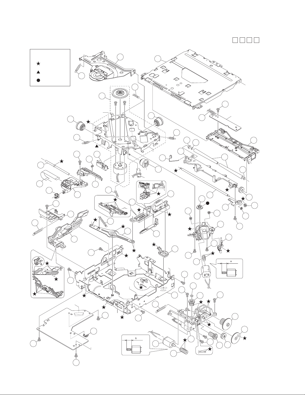
CD mechanism assembly and parts list
FMU-CD4-21D
Grease
JVG-31N
42
10
Block No.
MMMB
D
29
62
61
FG-87HS
JVS-1003
E
33
F
9
43
44
A
24
50
F
46
47
64
Photo board
44
44
32
45
31
D
66
46
C
Rest switch board
30
28
44
Back side
6
4
8
G
23
2
5
3
60
67
49
57
58
B
59
B
35
39
56
51
35
36
53
55
54
52
40
37
G
48
7
37
11.1mm
38
0.1mm
A
48
34
48
C
1
E
61
14
21
16
14
3-6
63
Mecha
control
board
63
H
63
48
65
11.1mm
0.1mm
H
11
13
12
17
20
19
18
15
The parts without symbol number are not service.
Page 59

CD mechanism
Symbol No. Part No. Part Name Description Local
1 LV11598-001A MECHA FRAME
2 LV36800-002A LINK ARM
3 LV22300-002A SLIDE CAM (L)
4 LV22298-002A SLIDE CAM(R)
5 LV36802-001A LOAD RACK
6 LV44552-001A RETURN SPRING
7 LV36803-002A F LOCK LEVER
8 LV36804-002A CAM COVER
9 VKZ4539-054 MINI SCREW
10 LV11260-003A TOP COVER
11 QAR0373-002 MOTOR
12 QYSPSPT2025MA SCREW M2 x 2.5mm(x2)
13 LV36903-003A L M BASE ASSY
14 VKZ4539-054 MINI SCREW (x2)
15 LV36806-001A L WORM GEAR
16 LV36805-002A M WHEEL GEAR
17 LV36807-001A A WHEEL GEAR
18 LV36808-001A R ACT GEAR(1)
19 LV36809-001A LOAD ACT GEAR
20 LV36810-001A LOADING GEAR
21 QYWDL1230250 SLIT WASHER 3mm/1.2mm x 0.25mm
23 LV44658-001A LINK SPRING
24 CM-FLMCD1D SPINDLE MOTOR ASSY
28 QAL0993-001 PICK UP
29 LV44555-001A MAIN SHAFT
30 LV36799-001A RACK PLATE
31 LV45227-001A RACK SPRING
32 QYSPSGT1745ZA TAP SCREW M1.7 x 4.5mm
33 LV36813-001A SUB GUIDE CAP
34 QAR0144-003 MOTOR 2.0V DC
35 QYSPSPT2025MA SCREW M2 x 2.5mm(x2)
36 LV22296-001A F MOTOR HOLDER
37 VKZ4539-054 MINI SCREW (x2)
38 LV36814-001A F WORM GEAR
39 LV36815-002A F WHEEL GEAR
40 LV36816-001A TRIGGER ARM
42 LV37326-003A CLAMPER ASSY
43 LV44557-002A CLAMPER SPRING
44 LV44558-001A SUS SPRING (x4)
45 LV36820-001A WIRE HOLDER
46 LV36904-001A DAMPER (x2)
47 LV37061-001A DAMPER
48 VKZ4539-054 MINI SCREW (x4)
49 LV11264-003A DISC PLATE
50 LV44586-001A SPECIAL SCREW
51 LV36801-002A GEAR HOLDER
52 VKZ4539-054 MINI SCREW
53 LV36821-001A R ACT GEAR(2)
54 LV36822-001A R ACT GEAR(3)
55 LV36823-001A ROLLER GEAR
56 LV44559-003A ROLLER SHAFT
57 LV22744-001A R HOLDER ASSY 2
58 LV44560-001A ROLLER (x2)
59 LV44590-001A WASHER
60 LV45268-001A ROLLER COLLAR 2
61 LV44562-002A ROLLER SPRING (x2)
62 QAL0817-003 FPC
63 VKZ4539-054 MINI SCREW (x3)
64 WJS0085-001A-E E-FL/RB WIRE
65 LV34916-002A WIRE CLAMP
66 LV45269-001A R HOLDER ROD
67 LV45270-001A WASHER 2
Block No. [M][B][M][M]
3-7
Page 60

Electrical parts list
Old Main board
Block No. [0][1]
Symbol No.
IC1 TEF6606T/V3-X IC1
IC71 LC72725KM-X IC C,D,E,F
IC161 TDA7718-X IC
IC301 TDA7851A IC
IC381 NJM2160BV-X IC A
IC401 TPS2051BD-X IC
IC701 MN101EF16ZXW IC
IC702 S-80824CNNB-G-W IC
IC702 or IC-PST3424U-X IC
IC771 S-24CS04AFJ-G-X IC A,B,G,H,I,J,K,
IC771 S-24CS16A0I-G-X IC C,D,E,F
IC801 74AHCT126PW-X IC
IC901 AN34002A REGULATOR IC
IC931 BD9007HFP-W IC
Q331 IMX9-W PAIR TRANSISTOR
Q781 RT1P141C-X DIGI TRANSISTOR
Q781 or UN2111-X TRANSISTOR
Q782 or 2SC3928A/QR/-X TRANSISTOR
Q782 2SC1623A/5-6/-X TRANSISTOR
Q784 RT1P141C-X DIGI TRANSISTOR
Q784 or UN2111-X TRANSISTOR
Q881 RT1N141C-X DIGI TRANSISTOR
Q881 or UN2211-X TRANSISTOR
Q891 RT1N141C-X DIGI TRANSISTOR C,D,E,F
Q891 or UN2211-X TRANSISTOR C,D,E,F
Q976 RT1N141C-X DIGI TRANSISTOR
Q976 or UN2211-X TRANSISTOR
Q977 or ISA1530AC1/QR/X TRANSISTOR
Q977 2SA812A/5-6/-X TRANSISTOR
Q978 or 2SC3928A/QR/-X TRANSISTOR
Q978 2SC1623A/5-6/-X TRANSISTOR
D331 MC2836-X DIODE
D331 or MA152WA-X DIODE
D711 UDZW6.2B-X Z DIODE A,C,D,E,F
D711 or MA8062/M/-X Z DIODE A,C,D,E,F
D712 1SS355W-X DIODE
D712 or MA111-X SI DIODE
D715 or UDZW5.1B-X SB DIODE
D715 MA8051/M/-X Z DIODE
D716 or UDZW5.1B-X SB DIODE
D716 MA8051/M/-X Z DIODE
D717 or UDZW5.1B-X SB DIODE
D717 MA8051/M/-X Z DIODE
D718 or UDZW5.1B-X SB DIODE
D718 MA8051/M/-X Z DIODE
D719 or UDZW5.1B-X SB DIODE
D719 MA8051/M/-X Z DIODE
D720 or UDZW5.1B-X SB DIODE
D720 MA8051/M/-X Z DIODE
D781 1SS355W-X DIODE
D781 or MA111-X SI DIODE
D782 1SS355W-X DIODE
D782 or MA111-X SI DIODE
D784 UDZW11B-X Z DIODE
D784 or MA8110/M/-X Z DIODE
D785 1SS355W-X DIODE
D785 or MA111-X SI DIODE
D851 MA22D23-X SB DIODE G,H,I,J,K,L,M,
D851 or RB160M-30-X SB DIODE G,H,I,J,K,L,M,
D851 or CRS03-W SB DIODE G,H,I,J,K,L,M,
D852 MA22D23-X SB DIODE G,H,I,J,K,L,M,
D852 or RB160M-30-X SB DIODE G,H,I,J,K,L,M,
D852 or CRS03-W SB DIODE G,H,I,J,K,L,M,
D891 MC2836-X DIODE C,D,E,F
Part No. Part Name Description Local
L,M,N,O
N,O
N,O
N,O
N,O
N,O
N,O
Symbol No.
D891 or MA152WA-X DIODE C,D,E,F
D901 1N5401-F64 SI DIODE
D901 or 1N5401-TU-15 SI DIODE
D902 GS1J-X DIODE C,D,E,F
D931 RSX201L-30-X SB DIODE
D971 MA22D23-X SB DIODE
D971 or RB160M-30-X SB DIODE
D971 or CRS03-W SB DIODE
D972 MA22D23-X SB DIODE
D972 or RB160M-30-X SB DIODE
D972 or CRS03-W SB DIODE
C1 NCB31HK-102X C CAPACITOR 1000pF 50V K
C2 NDC31HJ-5R6X C CAPACITOR 5.6pF 50V J
C3 NCB31HK-102X C CAPACITOR 1000pF 50V K
C4 NCB31AK-224X C CAPACITOR 0.22uF 10V K
C5 NDC31HJ-150X C CAPACITOR 15pF 50V J
C6 NDC31HJ-220X C CAPACITOR 22pF 50V J
C10 NCB21AK-105X C CAPACITOR 1uF 10V K
C11 NCB31HK-103X C CAPACITOR 0.01uF 50V K
C12 NCB31HK-103X C CAPACITOR 0.01uF 50V K
C13 NCB21AK-105X C CAPACITOR 1uF 10V K
C14 NCB31AK-224X C CAPACITOR 0.22uF 10V K
C15 NCB31CK-104X C CAPACITOR 0.1uF 16V K
C16 NCB31HK-103X C CAPACITOR 0.01uF 50V K
C17 NCB31CK-104X C CAPACITOR 0.1uF 16V K
C18 NCB31HK-103X C CAPACITOR 0.01uF 50V K
C19 NCB31CK-104X C CAPACITOR 0.1uF 16V K
C22 NDC31HJ-150X C CAPACITOR 15pF 50V J
C23 NCB31CK-104X C CAPACITOR 0.1uF 16V K
C24 NCB31HK-103X C CAPACITOR 0.01uF 50V K
C25 NCB31HK-103X C CAPACITOR 0.01uF 50V K
C26 QEKJ1CM-107Z E CAPACITOR 100uF 16V M
C27 QEKJ1EM-106Z E CAPACITOR 10uF 25V M
C71 NDC31HJ-561X C CAPACITOR 560pF 50V J C,D,E,F
C72 NDC31HJ-331X C CAPACITOR 330pF 50V J C,D,E,F
C73 QEKJ1EM-106Z E CAPACITOR 10uF 25V M C,D,E,F
C74 NDC31HJ-330X C CAPACITOR 33pF 50V J C,D,E,F
C75 NDC31HJ-330X C CAPACITOR 33pF 50V J C,D,E,F
C76 NCB31HK-103X C CAPACITOR 0.01uF 50V K C,D,E,F
C77 QEKJ0JM-476Z E CAPACITOR 47uF 6.3V M C,D,E,F
C78 NCB31HK-122X C CAPACITOR 1200pF 50V K C,D,E,F
C161 NCB31AK-105X C CAPACITOR 1uF 10V K
C162 QTE1H57-105Z E CAPACITOR 1uF 50V
C164 NCB31AK-105X C CAPACITOR 1uF 10V K
C165 NCB31AK-105X C CAPACITOR 1uF 10V K
C171 NCB31AK-105X C CAPACITOR 1uF 10V K
C172 QTE1H57-105Z E CAPACITOR 1uF 50V
C174 NCB31AK-105X C CAPACITOR 1uF 10V K
C177 NCB31AK-224X C CAPACITOR 0.22uF 10V K
C178 QTE1C57-106Z E CAPACITOR 10uF 16V
C183 QEKJ1AM-227Z E CAPACITOR 220uF 10V M
C184 NCB31CK-104X C CAPACITOR 0.1uF 16V K
C301 QFV91HJ-474Z MF CAPACITOR 0.47uF 50V J
C302 QFV91HJ-474Z MF CAPACITOR 0.47uF 50V J
C311 QFV91HJ-474Z MF CAPACITOR 0.47uF 50V J
C312 QFV91HJ-474Z MF CAPACITOR 0.47uF 50V J
C315 NCB31AK-105X C CAPACITOR 1uF 10V K
C316 QEKJ1HM-475Z E CAPACITOR 4.7uF 50V M
C317 QTE1C57-476Z E CAPACITOR 47uF 16V
C318 NCB21AK-225X-A C CAPACITOR 2.2uF 10V K
C319 NCB31EK-223X C CAPACITOR 0.022uF 25V K
C320 NCB31EK-223X C CAPACITOR 0.022uF 25V K
C322 NCB31HK-103X C CAPACITOR 0.01uF 50V K
C323 NCB31HK-103X C CAPACITOR 0.01uF 50V K
C324 NCB31HK-103X C CAPACITOR 0.01uF 50V K
C326 QEKJ1CM-226Z E CAPACITOR 22uF 16V M
C340 NDC31HJ-820X C CAPACITOR 82pF 50V J
C381 QEKJ1HM-475Z E CAPACITOR 4.7uF 50V M
C382 QEKJ1HM-475Z E CAPACITOR 4.7uF 50V M
C383 QEKJ1HM-475Z E CAPACITOR 4.7uF 50V M A
C384 QEKJ1HM-475Z E CAPACITOR 4.7uF 50V M A
C385 NCB31EK-104X C CAPACITOR 0.1uF 25V K A
C386 NCB31EK-104X C CAPACITOR 0.1uF 25V K A
C387 NCB31HK-152X C CAPACITOR 1500pF 50V K A
C388 NCB31HK-152X C CAPACITOR 1500pF 50V K A
Part No. Part Name Description Local
3-8
Page 61

Symbol No.
Part No. Part Name Description Local
Symbol No.
Part No. Part Name Description Local
C389 QEKJ1CM-107Z E CAPACITOR 100uF 16V M A
C390 QEKJ1CM-107Z E CAPACITOR 100uF 16V M A
C392 QEKJ1CM-106Z E CAPACITOR 10uF 16V M A
C401 NDC31HJ-820X C CAPACITOR 82pF 50V J
C402 NDC31HJ-101X C CAPACITOR 100pF 50V J
C418 NDC31HJ-270X C CAPACITOR 27pF 50V J
C419 NDC31HJ-270X C CAPACITOR 27pF 50V J
C583 NCB21HK-332X C CAPACITOR 3300pF 50V K
C584 NCB21HK-332X C CAPACITOR 3300pF 50V K
C585 QTE1H64-225Z E CAPACITOR 2.2uF 50V
C586 QTE1H64-225Z E CAPACITOR 2.2uF 50V
C587 NDC31HJ-331X C CAPACITOR 330pF 50V J
C588 NDC31HJ-331X C CAPACITOR 330pF 50V J
C703 NDC31HJ-270X C CAPACITOR 27pF 50V J
C704 NDC31HJ-270X C CAPACITOR 27pF 50V J
C706 NDC31HJ-821X C CAPACITOR 820pF 50V J
C707 QEKJ1CM-107Z E CAPACITOR 100uF 16V M
C708 NCB31CK-104X C CAPACITOR 0.1uF 16V K
C709 NCB31CK-104X C CAPACITOR 0.1uF 16V K
C710 NDC31HJ-101X C CAPACITOR 100pF 50V J A,C,D,E,F
C711 QEKJ0JM-476Z E CAPACITOR 47uF 6.3V M
C714 NCB31CK-104X C CAPACITOR 0.1uF 16V K
C715 NCB31CK-104X C CAPACITOR 0.1uF 16V K
C717 NDC31HJ-821X C CAPACITOR 820pF 50V J
C718 NCB31CK-104X C CAPACITOR 0.1uF 16V K
C719 QERF1AM-107Z E CAPACITOR 100uF 10V M
C720 NDC31HJ-820X C CAPACITOR 82pF 50V J
C721 NCB31CK-104X C CAPACITOR 0.1uF 16V K
C722 QERF1EM-475Z E CAPACITOR 4.7uF 25V M
C728 NCB31AK-105X C CAPACITOR 1uF 10V K
C729 NCB31HK-392X C CAPACITOR 3900pF 50V K
C730 NCB31HK-392X C CAPACITOR 3900pF 50V K
C732 NCB31HK-122X C CAPACITOR 1200pF 50V K
C734 NDC31HJ-560X C CAPACITOR 56pF 50V J
C735 NDC31HJ-560X C CAPACITOR 56pF 50V J
C771 NCB31CK-473X C CAPACITOR 0.047uF 16V K
C781 QEKJ0JM-107Z E CAPACITOR 100uF 6.3V M
C784 QEKJ1CM-107Z E CAPACITOR 100uF 16V M
C801 NCB31CK-473X C CAPACITOR 0.047uF 16V K
C851 QEKJ1EM-106Z E CAPACITOR 10uF 25V M G,H,I,J,K,L,M,
C852 NCB31CK-224X C CAPACITOR 0.22uF 16V K G,H,I,J,K,L,M,
C881 QERF1CM-226Z E CAPACITOR 22uF 16V M
C891 NCB31CK-104X C CAPACITOR 0.1uF 16V K C,D,E,F
C901 QEZ0870-278 E CAPACITOR 2700uF
C902 QERF1HM-225Z E CAPACITOR 2.2uF 50V M
C903 QEKJ1CM-107Z E CAPACITOR 100uF 16V M
C905 QEKJ1CM-476Z E CAPACITOR 47uF 16V M
C906 NCB31HK-103X C CAPACITOR 0.01uF 50V K
C907 QERF1AM-227Z E CAPACITOR 220uF 10V M
C908 QERF1AM-227Z E CAPACITOR 220uF 10V M
C909 QERF0JM-337Z E CAPACITOR 330uF 6.3V M
C910 QEKJ1EM-106Z E CAPACITOR 10uF 25V M
C912 NCB31HK-103X C CAPACITOR 0.01uF 50V K
C913 QEKJ1EM-106Z E CAPACITOR 10uF 25V M
C914 QEKJ1CM-107Z E CAPACITOR 100uF 16V M
C916 NCB31HK-103X C CAPACITOR 0.01uF 50V K
C928 NCB31HK-472X C CAPACITOR 4700pF 50V K
C931 QEZ0595-477Z E CAPACITOR 470uF 25V M
C932 QBZ0006-337Z TA E CAPACITOR 330uF
C933 NCB31HK-152X C CAPACITOR 1500pF 50V K
C937 NCB21CK-475X C CAPACITOR 4.7uF 16V K
C938 NCJ21EK-225X-D C CAPACITOR 2.2uF 25V K
C940 NDC31HJ-180X C CAPACITOR 18pF 50V J
C971 NCB31EK-104X C CAPACITOR 0.1uF 25V K
C992 NDC31HJ-101X C CAPACITOR 100pF 50V J
R2 NRSA63J-824X MG RESISTOR 820k
R3 NRSA63J-0R0X MG RESISTOR 0
R4 NRSA63J-472X MG RESISTOR 4.7k
R5 NRS181J-220X MG RESISTOR 22
R6 NRSA63J-101X MG RESISTOR 100
R7 NRSA63J-101X MG RESISTOR 100
R10 NRSA63J-0R0X MG RESISTOR 0
R11 NRS181J-4R7X MG RESISTOR 4.7
R12 NRZ0084-0R0X MG RESISTOR 0
R14 NRSA63J-472X MG RESISTOR 4.7k
Ω
Ω
1/10W J
Ω
1/16W J
Ω
1/8W J
Ω
1/16W J
Ω
1/16W J
Ω
1/10W J
Ω
1/8W J
Ω
Ω
1/16W J
N,O
N,O
1/16W J
C,D,E,F
R15 NRSA63J-472X MG RESISTOR 4.7kΩ 1/16W J
R71 NRSA63J-0R0X MG RESISTOR 0
R72 NRSA63J-222X MG RESISTOR 2.2k
R73 NRSA63J-222X MG RESISTOR 2.2k
R74 NRSA02J-101X MG RESISTOR 100
R81 NRSA63J-153X MG RESISTOR 15k
R81 NRSA63J-682X MG RESISTOR 6.8k
R82 NRSA63J-822X MG RESISTOR 8.2k
R82 NRSA63J-682X MG RESISTOR 6.8k
R91 NRSA63J-153X MG RESISTOR 15k
R91 NRSA63J-682X MG RESISTOR 6.8k
R92 NRSA63J-822X MG RESISTOR 8.2k
R92 NRSA63J-682X MG RESISTOR 6.8k
R161 NRSA63J-472X MG RESISTOR 4.7k
R162 NRSA63J-472X MG RESISTOR 4.7k
R171 NRSA63J-101X MG RESISTOR 100
R172 NRSA63J-101X MG RESISTOR 100
R305 NRSA63J-102X MG RESISTOR 1k
R309 NRS181J-100X MG RESISTOR 10
R310 NRSA63J-472X MG RESISTOR 4.7k
R341 NRSA63J-222X MG RESISTOR 2.2k
R342 NRSA63J-821X MG RESISTOR 820
R343 NRSA02J-101X MG RESISTOR 100
R344 NRSA63J-473X MG RESISTOR 47k
R351 NRSA63J-222X MG RESISTOR 2.2k
R352 NRSA63J-821X MG RESISTOR 820
R353 NRSA02J-101X MG RESISTOR 100
R354 NRSA63J-473X MG RESISTOR 47k
R381 NRSA63J-102X MG RESISTOR 1k
R382 NRSA63J-102X MG RESISTOR 1k
R383 NRSA63J-104X MG RESISTOR 100k
R384 NRSA63J-104X MG RESISTOR 100k
R385 NRSA63J-223X MG RESISTOR 22k
R386 NRSA63J-223X MG RESISTOR 22k
R387 NRSA63J-333X MG RESISTOR 33k
R388 NRSA63J-333X MG RESISTOR 33k
R389 NRSA63J-0R0X MG RESISTOR 0
R390 NRSA63J-0R0X MG RESISTOR 0
R583 NRSA63J-153X MG RESISTOR 15k
R584 NRSA63J-153X MG RESISTOR 15k
R585 NRSA63J-102X MG RESISTOR 1k
R586 NRSA63J-102X MG RESISTOR 1k
R587 NRSA63J-183X MG RESISTOR 18k
R588 NRSA63J-183X MG RESISTOR 18k
R701 NRSA63J-103X MG RESISTOR 10k
R702 NRSA63J-103X MG RESISTOR 10k
R703 NRSA63J-104X MG RESISTOR 100k
R704 NRSA63J-104X MG RESISTOR 100k
R708 NRSA63J-104X MG RESISTOR 100k
R709 NRSA63J-473X MG RESISTOR 47k
R711 NRSA63J-473X MG RESISTOR 47k
R712 NRSA63J-331X MG RESISTOR 330
R714 NRSA63J-0R0X MG RESISTOR 0
R717 NRSA63J-102X MG RESISTOR 1k
R718 NRSA63J-102X MG RESISTOR 1k
R719 NRSA63J-102X MG RESISTOR 1k
R720 NRSA63J-102X MG RESISTOR 1k
R721 NRSA63J-102X MG RESISTOR 1k
R722 NRS181J-102X MG RESISTOR 1k
R723 NRSA63J-102X MG RESISTOR 1k
R724 NRSA63J-102X MG RESISTOR 1k
R725 NRSA63J-102X MG RESISTOR 1k
R726 NRSA63J-273X MG RESISTOR 27k
R727 NRSA63J-122X MG RESISTOR 1.2k
R728 NRSA63J-102X MG RESISTOR 1k
R730 NRSA63J-102X MG RESISTOR 1k
R731 NRSA63J-101X MG RESISTOR 100
R732 NRSA63J-473X MG RESISTOR 47k
R733 NRSA63J-473X MG RESISTOR 47k
R734 NRSA63J-471X MG RESISTOR 470
R736 NRSA63J-561X MG RESISTOR 560
R737 NRSA63J-561X MG RESISTOR 560
Ω
1/10W J C,D,E,F
Ω
1/16W J C,D,E,F
Ω
1/16W J C,D,E,F
Ω
1/10W J C,D,E,F
Ω
1/16W J A,B
Ω
1/16W J C,D,E,F,G,H,I,
Ω
1/16W J A,B
Ω
1/16W J C,D,E,F,G,H,I,
Ω
1/16W J A,B
Ω
1/16W J C,D,E,F,G,H,I,
Ω
1/16W J A,B
Ω
1/16W J C,D,E,F,G,H,I,
Ω
1/16W J
Ω
1/16W J
Ω
1/16W J
Ω
1/16W J
Ω
1/16W J
Ω
1/8W J
Ω
1/16W J
Ω
1/16W J
Ω
1/16W J
Ω
1/10W J
Ω
1/16W J
Ω
1/16W J
Ω
1/16W J
Ω
1/10W J
Ω
1/16W J
Ω
1/16W J A
Ω
1/16W J A
Ω
1/16W J A
Ω
1/16W J A
Ω
1/16W J A
Ω
1/16W J A
Ω
1/16W J A
Ω
1/16W J A
Ω
1/10W J B,C,D,E,F,G,H
Ω
1/10W J B,C,D,E,F,G,H
Ω
1/16W J
Ω
1/16W J
Ω
1/16W J
Ω
1/16W J
Ω
1/16W J
Ω
1/16W J
Ω
1/16W J
Ω
1/16W J
Ω
1/16W J
Ω
1/16W J
Ω
1/16W J A,B
Ω
1/16W J C,D,E,F,G,H,I,
Ω
1/16W J
Ω
1/16W J
Ω
1/10W J
Ω
1/16W J
Ω
1/16W J
Ω
1/16W J
Ω
1/16W J
Ω
1/16W J
Ω
1/8W J
Ω
1/16W J
Ω
1/16W J
Ω
1/16W J
Ω
1/16W J
Ω
1/16W J
Ω
1/16W J
Ω
1/16W J
Ω
1/16W J
Ω
1/16W J
Ω
1/16W J
Ω
1/16W J
Ω
1/16W J
Ω
1/16W J
J,K,L,M,N,O
J,K,L,M,N,O
J,K,L,M,N,O
J,K,L,M,N,O
,I,J,K,L,M,N,O
,I,J,K,L,M,N,O
J,K,L,M,N,O
3-9
Page 62

Symbol No.
Part No. Part Name Description Local
Symbol No.
Part No. Part Name Description Local
R738 NRSA63J-561X MG RESISTOR 560Ω 1/16W J
R739 NRSA63J-101X MG RESISTOR 100
R740 NRSA63J-561X MG RESISTOR 560
R741 NRSA63J-101X MG RESISTOR 100
R742 NRSA63J-101X MG RESISTOR 100
R743 NRSA63J-101X MG RESISTOR 100
R744 NRSA63J-101X MG RESISTOR 100
R745 NRSA63J-271X MG RESISTOR 270
R746 NRSA63J-104X MG RESISTOR 100k
R747 NRSA63J-103X MG RESISTOR 10k
R748 NRSA63J-122X MG RESISTOR 1.2k
R749 NRSA63J-102X MG RESISTOR 1k
R750 NRS181J-104X MG RESISTOR 100k
R752 NRSA63J-472X MG RESISTOR 4.7k
R753 NRSA63J-472X MG RESISTOR 4.7k
R755 NRSA63J-472X MG RESISTOR 4.7k
R756 NRSA63J-472X MG RESISTOR 4.7k
R757 NRSA63J-122X MG RESISTOR 1.2k
R758 NRSA63J-473X MG RESISTOR 47k
R760 NRSA63J-122X MG RESISTOR 1.2k
R761 NRSA63J-122X MG RESISTOR 1.2k
R762 NRSA63J-122X MG RESISTOR 1.2k
R763 NRSA63J-823X MG RESISTOR 82k
R764 NRSA63J-823X MG RESISTOR 82k
R765 NRSA63J-472X MG RESISTOR 4.7k
R766 NRS181J-472X MG RESISTOR 4.7k
R767 NRSA63J-473X MG RESISTOR 47k
R768 NRSA63J-472X MG RESISTOR 4.7k
R770 NRSA63J-222X MG RESISTOR 2.2k
R771 NRSA63J-271X MG RESISTOR 270
R772 NRSA63J-271X MG RESISTOR 270
R773 NRSA63J-223X MG RESISTOR 22k
R774 NRSA63J-473X MG RESISTOR 47k
R775 NRSA63J-222X MG RESISTOR 2.2k
R777 NRSA63J-103X MG RESISTOR 10k
R779 NRSA63J-101X MG RESISTOR 100
R781 NRSA63J-473X MG RESISTOR 47k
R782 NRSA63J-472X MG RESISTOR 4.7k
R783 NRSA63J-103X MG RESISTOR 10k
R784 NRSA63J-0R0X MG RESISTOR 0
R801 NRSA63J-102X MG RESISTOR 1k
R802 NRSA63J-104X MG RESISTOR 100k
R803 NRSA63J-682X MG RESISTOR 6.8k
R804 NRSA63J-392X MG RESISTOR 3.9k
R805 NRS181J-0R0X MG RESISTOR 0
R806 NRS181J-102X MG RESISTOR 1k
R807 NRSA63J-104X MG RESISTOR 100k
R808 NRSA63J-101X MG RESISTOR 100
R809 NRSA63J-473X MG RESISTOR 47k
R810 NRSA63J-392X MG RESISTOR 3.9k
R811 NRSA63J-682X MG RESISTOR 6.8k
R812 NRSA63J-104X MG RESISTOR 100k
R813 NRSA63J-102X MG RESISTOR 1k
R814 NRSA63J-101X MG RESISTOR 100
R819 NRSA63J-473X MG RESISTOR 47k
R851 NRSA63J-103X MG RESISTOR 10k
R881 NRSA63J-473X MG RESISTOR 47k
R882 NRSA63J-472X MG RESISTOR 4.7k
R891 NRSA63J-102X MG RESISTOR 1k
R892 NRSA63J-473X MG RESISTOR 47k
R901 QRE142J-102X C RESISTOR 1k
R902 NRS181J-912X MG RESISTOR 9.1k
R903 NRSA02J-472X MG RESISTOR 4.7k
R928 NRSA63J-753X MG RESISTOR 75k
R929 NRSA63J-513X MG RESISTOR 51k
R930 NRSA63J-0R0X MG RESISTOR 0
R937 NRS181J-221X MG RESISTOR 220
R939 NRS181J-153X MG RESISTOR 15k
R940 NRSA63J-823X MG RESISTOR 82k
R971 NRS181J-332X MG RESISTOR 3.3k
R976 NRSA02J-273X MG RESISTOR 27k
R977 NRSA02J-123X MG RESISTOR 12k
L1 NQL093K-R47X COIL 0.47uH K
L3 QQL213M-R22Z COIL 0.22uH M
L4 QQR1813-001 COIL
L5 QQL244J-561Z COIL 560uH J
Ω
1/16W J
Ω
1/16W J
Ω
1/16W J
Ω
1/16W J
Ω
1/16W J C,D,E,F
Ω
1/16W J
Ω
1/16W J C,D,E,F
Ω
1/16W J
Ω
1/16W J
Ω
1/16W J
Ω
1/16W J
Ω
1/8W J
Ω
1/16W J
Ω
1/16W J
Ω
1/16W J
Ω
1/16W J
Ω
1/16W J
Ω
1/16W J
Ω
1/16W J
Ω
1/16W J
Ω
1/16W J
Ω
1/16W J
Ω
1/16W J
Ω
1/16W J
Ω
1/8W J
Ω
1/16W J
Ω
1/16W J
Ω
1/16W J A,B,C,D,E,F
Ω
1/16W J
Ω
1/16W J
Ω
1/16W J A,B,C,D,E,F
Ω
1/16W J
Ω
1/16W J
Ω
1/16W J
Ω
1/16W J
Ω
1/16W J
Ω
1/16W J
Ω
1/16W J
Ω
1/10W J
Ω
1/16W J
Ω
1/16W J
Ω
1/16W J
Ω
1/16W J
Ω
1/8W J
Ω
1/8W J
Ω
1/16W J
Ω
1/16W J
Ω
1/16W J
Ω
1/16W J
Ω
1/16W J
Ω
1/16W J
Ω
1/16W J
Ω
1/16W J
Ω
1/16W J
Ω
1/16W J G,H,I,J,K,L,M,
Ω
1/16W J
Ω
1/16W J
Ω
1/16W J C,D,E,F
Ω
1/16W J C,D,E,F
Ω
1/4W J
Ω
1/8W J
Ω
1/10W J
Ω
1/16W J
Ω
1/16W J
Ω
1/10W J
Ω
1/8W J
Ω
1/8W J
Ω
1/16W J
Ω
1/8W J
Ω
1/10W J
Ω
1/10W J
N,O
L6 QQL244J-561Z COIL 560uH J
L7 QQL244J-4R7Z P COIL 4.7uH J
L8 QQL244J-4R7Z P COIL 4.7uH J
L701 QQL244J-4R7Z P COIL 4.7uH J
L702 QQL244J-4R7Z P COIL 4.7uH J
L901 QQR1852-001 CHOKE COIL
L901 or QQR0703-001 CHOKE COIL
L931 QQL92AK-330Z COIL 33uH K
L932 NQR0007-002X FERRITE BEADS
L933 NQLH25M-4R7X COIL 4.7uH M
CN501 QGB2027ME-28 CONNECTOR B-B (1-28)
CN701 QGZ1101J1-24 CONNECTOR (1-24)
CN703 QNS0283-001 STEERING
CN901 QNZ0607-001 CAR CONNECTOR
J1 QNB0190-001 ANT TERMINAL
J321 QNN0832-001 PIN JACK A
J321 QNN0802-001 PIN JACK B,C,D,E,F,G,H
J801 QNZ0095-001 CONNECTOR
K161 NRSA02J-0R0X MG RESISTOR 0
K162 NRSA02J-0R0X MG RESISTOR 0
K163 NRSA02J-0R0X MG RESISTOR 0
S701 QSW0648-001Z TACT SWITCH
X1 QAX0928-001Z CRYSTAL
X71 QAX0926-001Z CRYSTAL C,D,E,F
X701 QAX0667-001Z C RESONATOR 8.000MHz
X702 QAX0401-001 CRYSTAL 32.768KHz
REMOTE
Ω
1/10W J
Ω
1/10W J
Ω
1/10W J
A,C,D,E,F
,I,J,K,L,M,N,O
Old Switch board
Block No. [0][2]
Symbol No.
IC601 NCP5623DTBR2G-X IC
IC661 PTC6526LQ-L IC
IC681 NJL29H380A REMOCON RCV
Q601 2SC1623A/5-6/-X TRANSISTOR
Q601 or 2SC3928A/QR/-X TRANSISTOR
Q602 UNR9211G-X TRANSISTOR
Q602 or DTC114EEB-X TRANSISTOR
Q604 2SA2174G-X TRANSISTOR
Q604 or 2SA1774/QR/-X TRANSISTOR
Q605 UN2222-X IC
Q605 or DTD143EK-X TRANSISTOR
Q607 2SA2174G-X TRANSISTOR
Q607 or 2SA1774/QR/-X TRANSISTOR
Q608 UN2222-X IC
Q608 or DTD143EK-X TRANSISTOR
Q610 2SA2174G-X TRANSISTOR
Q610 or 2SA1774/QR/-X TRANSISTOR
Q611 UN2222-X IC
Q611 or DTD143EK-X TRANSISTOR
D601 NSSM065T-X LED
D603 NSSM065T-X LED
D604 NSSM065T-X LED
D605 NSSM065T-X LED
D616 UDZW5.1B-X SB DIODE
D616 or MA8051/M/-X Z DIODE
D617 UDZW5.1B-X SB DIODE
D617 or MA8051/M/-X Z DIODE
D630 LHQ974/LM/-X LED
D631 LHQ974/LM/-X LED
D632 LHQ974/LM/-X LED
D650 MA8056/M/-X Z DIODE
D650 or UDZW5.6B-X Z DIODE
D661 MA111-X SI DIODE
D661 or 1SS355W-X DIODE
C604 NCB31CK-105X C CAPACITOR 1uF 16V K
C650 NCB31CK-104X C CAPACITOR 0.1uF 16V K
C651 NBE21CM-106X TA E CAPACITOR 10uF 16V M
Part No. Part Name Description Local
3-10
Page 63

Symbol No.
Part No. Part Name Description Local
Symbol No.
Part No. Part Name Description Local
C655 NCJ11EK-106X-R C CAPACITOR 10uF 25V
C661 NCB31CK-105X C CAPACITOR 1uF 16V K
C662 NDC31HJ-151X C CAPACITOR 150pF 50V J
C663 NCB31CK-223X C CAPACITOR 0.022uF 16V K
C665 NCB31CK-104X C CAPACITOR 0.1uF 16V K
C666 NCB31CK-104X C CAPACITOR 0.1uF 16V K
C682 NCB31EK-104X C CAPACITOR 0.1uF 25V K
C684 NCB31HK-472X C CAPACITOR 4700pF 50V K
C685 NCB31HK-472X C CAPACITOR 4700pF 50V K
Ω
R601 NRSA63J-821X MG RESISTOR 820
R602 NRSA63J-821X MG RESISTOR 820
R603 NRSA63J-122X MG RESISTOR 1.2k
R604 NRSA63J-182X MG RESISTOR 1.8k
R605 NRSA63J-272X MG RESISTOR 2.7k
R606 NRSA63J-392X MG RESISTOR 3.9k
R607 NRSA63J-392X MG RESISTOR 3.9k
R608 NRSA63J-821X MG RESISTOR 820
R609 NRSA63J-821X MG RESISTOR 820
R610 NRSA63J-122X MG RESISTOR 1.2k
R611 NRSA63J-182X MG RESISTOR 1.8k
R612 NRSA63J-272X MG RESISTOR 2.7k
R613 NRSA63J-103X MG RESISTOR 10k
R614 NRSA63F-154X MG RESISTOR 150k
R615 NRSA63J-101X MG RESISTOR 100
R618 NRSA63J-101X MG RESISTOR 100
R626 NRSA63J-0R0X MG RESISTOR 0
R630 NRSA63J-271X MG RESISTOR 270
R631 NRS181J-471X MG RESISTOR 470
R634 NRSA63J-681X MG RESISTOR 680
R636 NRSA63J-222X MG RESISTOR 2.2k
R637 NRSA63J-222X MG RESISTOR 2.2k
R638 NRSA63J-222X MG RESISTOR 2.2k
R644 NRSA63J-122X MG RESISTOR 1.2k
R645 NRSA63J-122X MG RESISTOR 1.2k
R646 NRSA63J-162X MG RESISTOR 1.6k
R647 NRSA63J-911X MG RESISTOR 910
R648 NRSA63J-911X MG RESISTOR 910
R649 NRSA63J-122X MG RESISTOR 1.2k
R651 NRSA63J-102X MG RESISTOR 1k
R652 NRSA63J-0R0X MG RESISTOR 0
R656 NRS181J-331X MG RESISTOR 330
R657 NRS181J-331X MG RESISTOR 330
R658 NRS181J-621X MG RESISTOR 620
R660 NRSA63J-394X MG RESISTOR 390k
R661 NRSA63J-102X MG RESISTOR 1k
R662 NRSA63J-102X MG RESISTOR 1k
R663 NRSA63J-102X MG RESISTOR 1k
R664 NRSA63J-224X MG RESISTOR 220k
R665 NRSA63J-101X MG RESISTOR 100
R666 NRSA63J-101X MG RESISTOR 100
R667 NRSA63J-101X MG RESISTOR 100
R670 NRSA63J-103X MG RESISTOR 10k
R671 NRSA63J-103X MG RESISTOR 10k
R672 NRSA63J-101X MG RESISTOR 100
R673 NRSA63J-101X MG RESISTOR 100
R681 NRSA63J-471X MG RESISTOR 470
R682 NRSA63J-102X MG RESISTOR 1k
R6043 NRSA63J-0R0X MG RESISTOR 0
R6044 NRSA63J-0R0X MG RESISTOR 0
L602 NQR0536-001X CHOKE COIL
CJ601 QGZ1101K1-24 CONNECTOR (1-24)
CN603 QNZ1006-001 USB JACK
J601 QNS0215-001 3.5 JACK
JS686 QSW1263-001 ROTARY ENCODER
K670 NQR0007-002X FERRITE BEADS
K671 NQR0007-002X FERRITE BEADS
K672 NQR0007-002X FERRITE BEADS
K673 NRSA02J-0R0X MG RESISTOR 0
S601 NSW0124-001X TACT SW
S602 NSW0316-001X TACT SWITCH
S603 NSW0316-001X TACT SWITCH
S604 NSW0316-001X TACT SWITCH
S605 NSW0316-001X TACT SWITCH
S606 NSW0316-001X TACT SWITCH
S607 NSW0316-001X TACT SWITCH
1/16W J
Ω
1/16W J
Ω
1/16W J
Ω
1/16W J
Ω
1/16W J
Ω
1/16W J
Ω
1/16W J
Ω
1/16W J
Ω
1/16W J
Ω
1/16W J
Ω
1/16W J
Ω
1/16W J
Ω
1/16W J
Ω
Ω
1/16W J
Ω
1/16W J
Ω
1/10W J
Ω
1/16W J
Ω
1/8W J
Ω
1/16W J
Ω
1/16W J
Ω
1/16W J
Ω
1/16W J
Ω
1/16W J
Ω
1/16W J
Ω
1/16W J
Ω
1/16W J
Ω
1/16W J
Ω
1/16W J
Ω
1/16W J
Ω
1/10W J
Ω
1/8W J
Ω
1/8W J
Ω
1/8W J
Ω
Ω
1/16W J
Ω
1/16W J
Ω
1/16W J
Ω
Ω
1/16W J
Ω
1/16W J
Ω
1/16W J
Ω
1/16W J
Ω
1/16W J
Ω
1/16W J
Ω
1/16W J
Ω
1/16W J
Ω
1/16W J
Ω
1/10W J
Ω
1/10W J
Ω
1/10W J
1/16W F
1/16W J
1/16W J
S608 NSW0316-001X TACT SWITCH
S609 NSW0316-001X TACT SWITCH
S610 NSW0316-001X TACT SWITCH
S611 NSW0316-001X TACT SWITCH
S612 NSW0316-001X TACT SWITCH
Old Mecha control board
Block No. [0][3]
Symbol No.
IC301 MN6627946JC IC(MCU)
IC302 BR24L16F-W-X IC(DIGITAL)
IC303 MFI341S2162-X IC
IC501 LA6565-X IC
Q101 2SC3928A/R/-X TRANSISTOR
Q201 2SC3928A/R/-X TRANSISTOR
Q211 PS1191RB22/BC/X PHOTO
Q212 PS1191RB22/BC/X PHOTO
Q301 ISA1530AC1/RS/X TRANSISTOR
Q302 RT1N441C-X TRANSISTOR
Q303 RT1N441C-X TRANSISTOR
Q501 2SB1424/R/-W TRANSISTOR
D101 AN1105W21/AB/-X IR LED
D201 AN1105W21/AB/-X IR LED
D501 1SR154-400-X SI DIODE
D502 1SR154-400-X SI DIODE
D503 1SR154-400-X SI DIODE
C101 NCB31CK-104X C CAPACITOR 0.1uF 16V K
C102 NCB31CK-104X C CAPACITOR 0.1uF 16V K
C103 NCB31CK-104X C CAPACITOR 0.1uF 16V K
C104 NCB31CK-104X C CAPACITOR 0.1uF 16V K
C201 NCB31CK-104X C CAPACITOR 0.1uF 16V K
C301 NEAF0JM-226X E CAPACITOR 22uF 6.3V M
C302 NCB31CK-104X C CAPACITOR 0.1uF 16V K
C303 NEAF0JM-476X E CAPACITOR 47uF 6.3V M
C304 NCB31CK-104X C CAPACITOR 0.1uF 16V K
C305 NCB31CK-104X C CAPACITOR 0.1uF 16V K
C306 NCB31CK-104X C CAPACITOR 0.1uF 16V K
C307 NCB31CK-334X C CAPACITOR 0.33uF 16V K
C308 NCB31HK-102X C CAPACITOR 1000pF 50V K
C309 NCB31EK-823X C CAPACITOR 0.082uF 25V K
C310 NCB31HK-102X C CAPACITOR 1000pF 50V K
C311 NCB31CK-104X C CAPACITOR 0.1uF 16V K
C312 NCB31HK-153X C CAPACITOR 0.015uF 50V K
C313 NCJ21CK-475X-R C CAPACITOR 4.7uF 16V K
C314 NCB31HK-332X C CAPACITOR 3300pF 50V K
C315 NEAF0JM-476X E CAPACITOR 47uF 6.3V M
C316 NEAF0JM-476X E CAPACITOR 47uF 6.3V M
C317 NCB31HK-223X C CAPACITOR 0.022uF 50V K
C319 NCB31CK-334X C CAPACITOR 0.33uF 16V K
C321 NCB31HK-272X C CAPACITOR 2700pF 50V K
C322 NCB31CK-154X C CAPACITOR 0.15uF 16V K
C323 NEAF0JM-476X E CAPACITOR 47uF 6.3V M
C324 NCB31CK-104X C CAPACITOR 0.1uF 16V K
C325 NCJ20JK-106X-R C CAPACITOR 10uF 6.3V K
C326 NCJ20JK-106X-R C CAPACITOR 10uF 6.3V K
C327 NCB31CK-104X C CAPACITOR 0.1uF 16V K
C328 NCB31HK-681X C CAPACITOR 680pF 50V K
C329 NCB31CK-104X C CAPACITOR 0.1uF 16V K
C330 NCJ20JK-106X-R C CAPACITOR 10uF 6.3V K
C331 NCJ20JK-106X-R C CAPACITOR 10uF 6.3V K
C332 NCJ20JK-106X-R C CAPACITOR 10uF 6.3V K
C334 NCB31CK-104X C CAPACITOR 0.1uF 16V K
C335 NCB31CK-104X C CAPACITOR 0.1uF 16V K
C336 NCB31CK-104X C CAPACITOR 0.1uF 16V K
C337 NCB31CK-104X C CAPACITOR 0.1uF 16V K
C338 NCB31CK-104X C CAPACITOR 0.1uF 16V K
C339 NCB31CK-104X C CAPACITOR 0.1uF 16V K
C340 NCB31CK-104X C CAPACITOR 0.1uF 16V K
Part No. Part Name Description Local
TRANSISTOR
TRANSISTOR
3-11
Page 64

Symbol No.
Part No. Part Name Description Local
Symbol No.
Part No. Part Name Description Local
C341 NDC31HJ-270X C CAPACITOR 27pF 50V J
C342 NDC31HJ-270X C CAPACITOR 27pF 50V J
C343 NCB31CK-104X C CAPACITOR 0.1uF 16V K
C344 NCJ20JK-106X-R C CAPACITOR 10uF 6.3V K
C345 NCB31CK-104X C CAPACITOR 0.1uF 16V K
C346 NCB31CK-104X C CAPACITOR 0.1uF 16V K
C347 NCB31CK-104X C CAPACITOR 0.1uF 16V K
C351 NDC31HJ-270X C CAPACITOR 27pF 50V J
C352 NDC31HJ-270X C CAPACITOR 27pF 50V J
C373 NCB31CK-104X C CAPACITOR 0.1uF 16V K
C392 NCB31CK-104X C CAPACITOR 0.1uF 16V K
C393 NCB31CK-104X C CAPACITOR 0.1uF 16V K
C394 NCB31CK-104X C CAPACITOR 0.1uF 16V K
C395 NCB31CK-104X C CAPACITOR 0.1uF 16V K
C501 NEHN1EM-476X E CAPACITOR 47uF 25V M
C502 NCB31CK-104X C CAPACITOR 0.1uF 16V K
C503 NDC31HJ-680X C CAPACITOR 68pF 50V J
C511 NCB31HK-682X C CAPACITOR 6800pF 50V K
C512 NCB31HK-222X C CAPACITOR 2200pF 50V K
C513 NCB31HK-272X C CAPACITOR 2700pF 50V K
C514 NCB31HK-122X C CAPACITOR 1200pF 50V K
C531 NEHL0JM-107X E CAPACITOR 100uF 6.3V M
C532 NCB31CK-104X C CAPACITOR 0.1uF 16V K
C551 NEHN1AM-107X E CAPACITOR 100uF 10V M
Ω
R101 NRSA63J-391X MG RESISTOR 390
R102 NRSA63J-822X MG RESISTOR 8.2k
R103 NRSA63J-184X MG RESISTOR 180k
R104 NRSA63J-184X MG RESISTOR 180k
R105 NRSA63J-183X MG RESISTOR 18k
R201 NRSA63J-391X MG RESISTOR 390
R203 NRSA63J-184X MG RESISTOR 180k
R204 NRSA63J-184X MG RESISTOR 180k
R205 NRSA63J-153X MG RESISTOR 15k
R206 NRSA63J-473X MG RESISTOR 47k
R207 NRSA63J-473X MG RESISTOR 47k
R214 NRSA63D-153X MG RESISTOR 15k
R215 NRSA63D-153X MG RESISTOR 15k
R216 NRS181F-300X MG RESISTOR 30
R217 NRS181F-300X MG RESISTOR 30
R228 NRSA63J-103X MG RESISTOR 10k
R229 NRSA63J-103X MG RESISTOR 10k
R230 NRSA63J-103X MG RESISTOR 10k
R241 NRSA63J-473X MG RESISTOR 47k
R242 NRSA63J-102X MG RESISTOR 1k
R301 NRSA63J-100X MG RESISTOR 10
R302 NRSA63J-473X MG RESISTOR 47k
R304 NRSA63J-100X MG RESISTOR 10
R307 NRSA63J-102X MG RESISTOR 1k
R308 NRSA63J-104X MG RESISTOR 100k
R309 NRSA63J-104X MG RESISTOR 100k
R310 NRSA63J-473X MG RESISTOR 47k
R311 NRSA63J-101X MG RESISTOR 100
R312 NRSA63J-101X MG RESISTOR 100
R313 NRSA63J-101X MG RESISTOR 100
R314 NRSA63J-272X MG RESISTOR 2.7k
R315 NRSA63J-821X MG RESISTOR 820
R316 NRSA63J-823X MG RESISTOR 82k
R317 NRSA63J-473X MG RESISTOR 47k
R318 NRSA63J-473X MG RESISTOR 47k
R319 NRSA63J-0R0X MG RESISTOR 0
R320 NRSA63J-0R0X MG RESISTOR 0
R321 NRSA63J-0R0X MG RESISTOR 0
R322 NRSA63J-822X MG RESISTOR 8.2k
R323 NRSA63J-822X MG RESISTOR 8.2k
R324 NRSA63J-473X MG RESISTOR 47k
R325 NRSA02F-100X MG RESISTOR 10
R326 NRSA02F-100X MG RESISTOR 10
R327 NRSA63J-101X MG RESISTOR 100
R328 NRSA63J-101X MG RESISTOR 100
R329 NRSA63J-101X MG RESISTOR 100
R330 NRSA63J-473X MG RESISTOR 47k
R331 NRSA63J-151X MG RESISTOR 150
R332 NRSA63J-105X MG RESISTOR 1M
R333 NRSA63J-221X MG RESISTOR 220
R334 NRSA63J-473X MG RESISTOR 47k
R336 NRSA63J-330X MG RESISTOR 33
R337 NRSA63J-473X MG RESISTOR 47k
1/16W J
Ω
Ω
Ω
Ω
1/16W J
Ω
1/16W J
Ω
Ω
Ω
1/16W J
Ω
1/16W J
Ω
1/16W J
Ω
1/16W D
Ω
1/16W D
Ω
1/8W F
Ω
1/8W F
Ω
1/16W J
Ω
1/16W J
Ω
1/16W J
Ω
1/16W J
Ω
1/16W J
Ω
1/16W J
Ω
1/16W J
Ω
1/16W J
Ω
1/16W J
Ω
Ω
Ω
1/16W J
Ω
1/16W J
Ω
1/16W J
Ω
1/16W J
Ω
Ω
1/16W J
Ω
1/16W J
Ω
1/16W J
Ω
1/16W J
Ω
1/16W J
Ω
1/16W J
Ω
1/16W J
Ω
Ω
Ω
1/16W J
Ω
1/10W F
Ω
1/10W F
Ω
1/16W J
Ω
1/16W J
Ω
1/16W J
Ω
1/16W J
Ω
1/16W J
Ω
1/16W J
Ω
1/16W J
Ω
1/16W J
Ω
1/16W J
Ω
1/16W J
1/16W J
1/16W J
1/16W J
1/16W J
1/16W J
1/16W J
1/16W J
1/16W J
1/16W J
1/16W J
R342 NRSA63J-0R0X MG RESISTOR 0Ω 1/16W J
R343 NRSA63J-472X MG RESISTOR 4.7k
R345 NRSA63J-472X MG RESISTOR 4.7k
R349 NRSA63J-0R0X MG RESISTOR 0
R361 NRSA63J-103X MG RESISTOR 10k
R362 NRSA63J-221X MG RESISTOR 220
R371 NRSA63J-0R0X MG RESISTOR 0
R501 NRS125J-100X MG RESISTOR 10
R503 NRSA63J-822X MG RESISTOR 8.2k
R504 NRSA63J-512X MG RESISTOR 5.1k
R505 NRSA63J-333X MG RESISTOR 33k
R506 NRSA63J-683X MG RESISTOR 68k
R507 NRSA63J-682X MG RESISTOR 6.8k
R508 NRSA63J-153X MG RESISTOR 15k
R509 NRSA63J-183X MG RESISTOR 18k
R510 NRSA63J-683X MG RESISTOR 68k
R511 NRSA63J-103X MG RESISTOR 10k
R512 NRSA63J-153X MG RESISTOR 15k
R513 NRSA63J-822X MG RESISTOR 8.2k
R514 NRSA63J-133X MG RESISTOR 13k
R515 NRSA63J-562X MG RESISTOR 5.6k
R516 NRSA63J-562X MG RESISTOR 5.6k
R519 NRSA63J-822X MG RESISTOR 8.2k
R520 NRSA63J-822X MG RESISTOR 8.2k
R521 NRSA63J-822X MG RESISTOR 8.2k
R522 NRSA63J-822X MG RESISTOR 8.2k
R523 NRSA63J-822X MG RESISTOR 8.2k
R524 NRSA63J-822X MG RESISTOR 8.2k
R525 NRSA63J-473X MG RESISTOR 47k
CN101 QGB2027L5-28X CONNECTOR B-B (1-28)
CN102 QGF0522F3-15W CONNECTOR FFC/FPC (1-15)
K101 NRSA63J-0R0X MG RESISTOR 0
K102 NRSA63J-0R0X MG RESISTOR 0
K103 NRSA63J-0R0X MG RESISTOR 0
SW1 NSW0291-001X DETECT SWITCH
X301 NAX0375-001X CRYSTAL 16.9344MHz
X302 NAX0367-001X CRYSTAL
Ω
Ω
Ω
1/16W J
Ω
1/16W J
Ω
1/16W J
Ω
1/16W J
Ω
1/2W J
Ω
Ω
Ω
1/16W J
Ω
1/16W J
Ω
Ω
1/16W J
Ω
1/16W J
Ω
1/16W J
Ω
1/16W J
Ω
1/16W J
Ω
Ω
1/16W J
Ω
Ω
Ω
Ω
Ω
Ω
Ω
Ω
Ω
1/16W J
Ω
1/16W J
Ω
1/16W J
Ω
1/16W J
1/16W J
1/16W J
1/16W J
1/16W J
1/16W J
1/16W J
1/16W J
1/16W J
1/16W J
1/16W J
1/16W J
1/16W J
1/16W J
1/16W J
Main board
Block No. [0][4]
Symbol No.
IC1 TEF6606T/V5-X IC
IC71 LC72725KM-X IC C,D,E,F
IC161 TDA7718-X IC
IC301 TDA7851A IC
IC381 NJM2160BV-X IC A
IC401 TPS2051BD-X IC
IC701 MN101E16YFE IC A,B,G,H,I,J,K,
IC701 MN101E16YFF IC C,D,E,F
IC702 S-80824CNNB-G-W IC
IC702 or IC-PST3424U-X IC
IC771 S-24CS04AFJ-G-X IC A,B,G,H,I,J,K,
IC771 S-24CS16A0I-G-X IC C,D,E,F
IC801 74AHCT126PW-X IC
IC901 AN34002A REGULATOR IC
IC931 BD9007HFP-W IC
Q331 IMX9-W PAIR TRANSISTOR
Q781 RT1P141C-X DIGI TRANSISTOR
Q781 or UN2111-X TRANSISTOR
Q782 or 2SC3928A/QR/-X TRANSISTOR
Q782 2SC1623A/5-6/-X TRANSISTOR
Q784 RT1P141C-X DIGI TRANSISTOR
Q784 or UN2111-X TRANSISTOR
Q881 RT1N141C-X DIGI TRANSISTOR
Q881 or UN2211-X TRANSISTOR
Q891 RT1N141C-X DIGI TRANSISTOR C,D,E,F
Q891 or UN2211-X TRANSISTOR C,D,E,F
Q976 RT1N141C-X DIGI TRANSISTOR
Q976 or UN2211-X TRANSISTOR
Part No. Part Name Description Local
L,M,N,O,P
L,M,N,O,P
3-12
Page 65

Symbol No.
Part No. Part Name Description Local
Symbol No.
Part No. Part Name Description Local
Q977 or ISA1530AC1/QR/X TRANSISTOR
Q977 2SA812A/5-6/-X TRANSISTOR
Q978 or 2SC3928A/QR/-X TRANSISTOR
Q978 2SC1623A/5-6/-X TRANSISTOR
D331 MC2836-X DIODE
D331 or MA152WA-X DIODE
D711 UDZW6.2B -X Z DIODE A,C,D,E,F
D711 or MA8062/M/-X Z DIODE A,C,D,E,F
D712 1SS355W-X DIODE
D712 or MA111-X SI DIODE
D715 UDZW5.1B-X SB DIODE
D715 or MA8051/M/-X Z DIODE
D716 UDZW5.1B-X SB DIODE
D716 or MA8051/M/-X Z DIODE
D717 UDZW5.1B-X SB DIODE
D717 or MA8051/M/-X Z DIODE
D718 UDZW5.1B-X SB DIODE
D718 or MA8051/M/-X Z DIODE
D719 UDZW5.1B-X SB DIODE
D719 or MA8051/M/-X Z DIODE
D720 UDZW5.1B-X SB DIODE
D720 or MA8051/M/-X Z DIODE
D781 1SS355W-X DIODE
D781 or MA111-X SI DIODE
D784 UDZW11B-X Z DIODE
D784 or MA8110/M/-X Z DIODE
D785 1SS355W-X DIODE
D785 or MA111-X SI DIODE
D851 MA22F20-X SB DIO DE G,H,I,J,K,L,M,
D852 MA22D23-X SB DIODE G,H,I,J,K,L,M,
D852 or RB160M-30-X SB DIODE G,H,I,J,K,L,M,
D852 or CRS03-W SB DIODE G,H,I,J,K,L,M,
D891 MC2836-X DIODE C,D,E,F
D891 or MA152WA-X DIODE C,D,E,F
D901 1N5401-F64 SI DIODE
D901 or 1N5401-TU-15 SI DIODE
D902 GS1J-LTP-X DIODE C,D,E,F
D931 RSX201L-30-X SB DIODE A,B,G,H,I,J,K,
D932 MA22D23-X SB DIODE C,D,E,F
D933 MA22D23-X SB DIODE C,D,E,F
D971 MA22F20-X SB DIODE
D972 MA22D23-X SB DIODE
D972 or RB160M-30-X SB DIODE
D972 or CRS03-W SB DIODE
C1 NCB31HK-102X C CAPACITOR 1000pF 50V K
C2 NDC31HJ-5R6X C CAPACITOR 5.6pF 50V J
C3 NCB31HK-102X C CAPACITOR 1000pF 50V K
C4 NCB31AK-224X C CAPACITOR 0.22uF 10V K
C5 NDC31HJ-150X C CAPACITOR 15pF 50V J
C6 NDC31HJ-220X C CAPACITOR 22pF 50V J
C10 NCB31AK-105X C CAPACITOR 1uF 10V K
C11 NCB31HK-103X C CAPACITOR 0.01uF 50V K
C12 NCB31HK-103X C CAPACITOR 0.01uF 50V K
C13 NCB31AK-105X C CAPACITOR 1uF 10V K
C14 NCB31AK-224X C CAPACITOR 0.22uF 10V K
C15 NCB31CK-104X C CAPACITOR 0.1uF 16V K
C16 NCB31HK-103X C CAPACITOR 0.01uF 50V K
C17 NCB31CK-104X C CAPACITOR 0.1uF 16V K
C18 NCB31HK-103X C CAPACITOR 0.01uF 50V K
C19 NCB31CK-104X C CAPACITOR 0.1uF 16V K
C22 NDC31HJ-150X C CAPACITOR 15pF 50V J
C23 NCB31CK-104X C CAPACITOR 0.1uF 16V K
C24 NCB31HK-103X C CAPACITOR 0.01uF 50V K
C25 NCB31HK-103X C CAPACITOR 0.01uF 50V K
C26 QEKJ1CM-107Z E CAPACITOR 100uF 16V M
C32 NDC31HJ-2R0X C CAPACITOR 2pF 50V J
C71 NDC31HJ-561X C CAPACITOR 560pF 50V J C,D,E,F
C72 NDC31HJ-331X C CAPACITOR 330pF 50V J C,D,E,F
C73 QEKJ1EM-106Z E CAPACITOR 10uF 25V M C,D,E,F
C74 NDC31HJ-330X C CAPACITOR 33pF 50V J C,D,E,F
C75 NDC31HJ-330X C CAPACITOR 33pF 50V J C,D,E,F
C76 NCB31HK-103X C CAPACITOR 0.01uF 50V K C,D,E,F
N,O
N,O
N,O
N,O
L,M,N,O,P
C78 NCB31HK-122X C CAPACITOR 1200pF 50V K C,D,E,F
C161 NCB31AK-105X C CAPACITOR 1uF 10V K
C162 QEKJ1HM-105Z E CAPACITOR 1uF 50V M
C164 NCB31AK-105X C CAPACITOR 1uF 10V K
C165 NCB31AK-105X C CAPACITOR 1uF 10V K
C166 NDC31HJ-560X C CAPACITOR 56pF 50V J
C171 NCB31AK-105X C CAPACITOR 1uF 10V K
C172 QEKJ1HM-105Z E CAPACITOR 1uF 50V M
C174 NCB31AK-105X C CAPACITOR 1uF 10V K
C176 NDC31HJ-560X C CAPACITOR 56pF 50V J
C177 NDC31HJ-560X C CAPACITOR 56pF 50V J
C178 QTE1C57-106Z E CAPACITOR 10uF 16V
C183 QEKJ1AM-227Z E CAPACITOR 220uF 10V M
C184 NCB31AK-105X C CAPACITOR 1uF 10V K
C301 QFV91HJ-474Z MF CAPACITOR 0.47uF 50V J
C302 QFV91HJ-474Z MF CAPACITOR 0.47uF 50V J
C311 QFV91HJ-474Z MF CAPACITOR 0.47uF 50V J
C312 QFV91HJ-474Z MF CAPACITOR 0.47uF 50V J
C315 NCB31AK-105X C CAPACITOR 1uF 10V K
C316 QEKJ1HM-475Z E CAPACITOR 4.7uF 50V M
C317 QTE1C57-476Z E CAPACITOR 47uF 16V
C318 NCB21AK-225X-A C CAPACITOR 2.2uF 10V K
C319 NCB31EK-223X C CAPACITOR 0.022uF 25V K
C320 NCB31EK-223X C CAPACITOR 0.022uF 25V K
C322 NCB31HK-103X C CAPACITOR 0.01uF 50V K
C323 NCB31HK-103X C CAPACITOR 0.01uF 50V K
C324 NCB31HK-103X C CAPACITOR 0.01uF 50V K
C326 QEKJ1CM-226Z E CAPACITOR 22uF 16V M
C340 NDC31HJ-820X C CAPACITOR 82pF 50V J
C345 NDC31HJ-560X C CAPACITOR 56pF 50V J
C346 NDC31HJ-560X C CAPACITOR 56pF 50V J
C347 NDC31HJ-560X C CAPACITOR 56pF 50V J
C348 NDC31HJ-560X C CAPACITOR 56pF 50V J
C381 QEKJ1HM-475Z E CAPACITOR 4.7uF 50V M
C382 QEKJ1HM-475Z E CAPACITOR 4.7uF 50V M
C383 QEKJ1HM-475Z E CAPACITOR 4.7uF 50V M A
C384 QEKJ1HM-475Z E CAPACITOR 4.7uF 50V M A
C385 NCB31EK-104X C CAPACITOR 0.1uF 25V K A
C386 NCB31EK-104X C CAPACITOR 0.1uF 25V K A
C387 NCB31HK-152X C CAPACITOR 1500pF 50V K A
C388 NCB31HK-152X C CAPACITOR 1500pF 50V K A
C389 QEKJ1CM-107Z E CAPACITOR 100uF 16V M A
C390 QEKJ1CM-107Z E CAPACITOR 100uF 16V M A
C392 QEKJ1CM-106Z E CAPACITOR 10uF 16V M A
C401 NDC31HJ-820X C CAPACITOR 82pF 50V J
C402 NDC31HJ-101X C CAPACITOR 100pF 50V J A,B,G,H,I,J,K,
C418 NDC31HJ-270X C CAPACITOR 27pF 50V J
C419 NDC31HJ-270X C CAPACITOR 27pF 50V J
C583 NCB31HK-332X C CAPACITOR 3300pF 50V K
C584 NCB31HK-332X C CAPACITOR 3300pF 50V K
C585 QTE1H64-225Z E CAPACITOR 2.2uF 50V
C586 QTE1H64-225Z E CAPACITOR 2.2uF 50V
C587 NDC31HJ-331X C CAPACITOR 330pF 50V J
C588 NDC31HJ-331X C CAPACITOR 330pF 50V J
C703 NDC31HJ-200X C CAPACITOR 20pF 50V J
C704 NDC31HJ-200X C CAPACITOR 20pF 50V J
C706 NDC31HJ-821X C CAPACITOR 820pF 50V J
C707 QEKJ1CM-107Z E CAPACITOR 100uF 16V M
C708 NCB31CK-104X C CAPACITOR 0.1uF 16V K
C709 NCB31CK-104X C CAPACITOR 0.1uF 16V K
C710 NDC31HJ-101X C CAPACITOR 100pF 50V J A,C,D,E,F
C711 QEKJ0JM-476Z E CAPACITOR 47uF 6.3V M
C714 NCB31CK-104X C CAPACITOR 0.1uF 16V K
C715 NCB31CK-104X C CAPACITOR 0.1uF 16V K
C717 NDC31HJ-821X C CAPACITOR 820pF 50V J
C718 NCB31CK-104X C CAPACITOR 0.1uF 16V K
C719 QERF1AM-107Z E CAPACITOR 100uF 10V M
C720 NDC31HJ-820X C CAPACITOR 82pF 50V J
C721 NCB31CK-104X C CAPACITOR 0.1uF 16V K
C722 QERF1EM-475Z E CAPACITOR 4.7uF 25V M
C728 NCB31AK-105X C CAPACITOR 1uF 10V K
C729 NCB31HK-392X C CAPACITOR 3900pF 50V K
C730 NCB31HK-392X C CAPACITOR 3900pF 50V K
C732 NCB31HK-122X C CAPACITOR 1200pF 50V K
C734 NDC31HJ-560X C CAPACITOR 56pF 50V J
C735 NDC31HJ-560X C CAPACITOR 56pF 50V J
C742 NDC31HJ-560X C CAPACITOR 56pF 50V J C,D,E,F
L,M,N,O,P
3-13
Page 66

Symbol No.
Part No. Part Name Description Local
Symbol No.
Part No. Part Name Description Local
C771 NCB31CK-473X C CAPACITOR 0.047uF 16V K
C781 QEKJ0JM-107Z E CAPACITOR 100uF 6.3V M
C784 QEKJ1CM-107Z E CAPACITOR 100uF 16V M
C801 NCB31CK-473X C CAPACITOR 0.047uF 16V K
C851 QEKJ1EM-106Z E CAPACITOR 10uF 25V M G,H,I,J,K,L,M,
C852 NCB31CK-224X C CAPACITOR 0.22uF 16V K G,H,I,J,K,L,M,
C881 QERF1CM-226Z E CAPACITOR 22uF 16V M
C891 NCB31CK-104X C CAPACITOR 0.1uF 16V K C,D,E,F
C901 QEZ0870-278 E CAPACITOR 2700uF
C903 QEKJ1CM-476Z E CAPACITOR 47uF 16V M
C905 QEKJ1CM-476Z E CAPACITOR 47uF 16V M
C906 NCB31HK-103X C CAPACITOR 0.01uF 50V K
C907 QEKJ1AM-107Z E CAPACITOR 100uF 10V M
C908 QEKJ1EM-475Z E CAPACITOR 4.7uF 25V M
C909 QEKJ0JM-227Z E CAPACITOR 220uF 6.3V M A,B,C,D,E,F,P
C909 QERF0JM-337Z E CAPACITOR 330uF 6.3V M G,H,I,J,K,L,M,
C910 QEKJ1EM-106Z E CAPACITOR 10uF 25V M
C912 NCB31HK-103X C CAPACITOR 0.01uF 50V K
C913 QEKJ1EM-106Z E CAPACITOR 10uF 25V M
C916 NCB31HK-103X C CAPACITOR 0.01uF 50V K
C918 NCB31HK-104X C CAPACITOR 0.1uF 50V K
C928 NCB31HK-472X C CAPACITOR 4700pF 50V K
C931 QEZ0595-477Z E CAPACITOR 470uF 25V M A,B,G,H,I,J,K,
C931 QETN1VM-477Z-S E CAPACITOR 470uF 35V M C,D,E,F
C932 QBZ0006-337Z TA E CAPACITOR 330uF
C933 NCB31HK-152X C CAPACITOR 1500pF 50V K
C937 NCB31AK-105X C CAPACITOR 1uF 10V K
C938 NCJ21EK-225X-D C CAPACITOR 2.2uF 25V K
C940 NDC31HJ-180X C CAPACITOR 18pF 50V J
C971 NCB31EK-104X C CAPACITOR 0.1uF 25V K
C992 NDC31HJ-220X C CAPACITOR 22pF 50V J
Ω
R2 NRSA63J-824X MG RESISTOR 820k
R4 NRSA63J-472X MG RESISTOR 4.7k
R5 NRS181J-220X MG RESISTOR 22
R6 NRSA63J-101X MG RESISTOR 100
R7 NRSA63J-101X MG RESISTOR 100
R10 NRSA63J-0R0X MG RESISTOR 0
R11 NRS181J-4R7X MG RESISTOR 4.7
R12 NRZ0084-0R0X MG RESISTOR 0
R14 NRSA63J-472X MG RESISTOR 4.7k
R15 NRSA63J-472X MG RESISTOR 4.7k
R71 NRSA63J-0R0X MG RESISTOR 0
R72 NRSA63J-222X MG RESISTOR 2.2k
R73 NRSA63J-222X MG RESISTOR 2.2k
R74 NRSA02J-101X MG RESISTOR 100
R81 NRSA63J-153X MG RESISTOR 15k
R81 NRSA63J-682X MG RESISTOR 6.8k
R82 NRSA63J-822X MG RESISTOR 8.2k
R82 NRSA63J-682X MG RESISTOR 6.8k
R91 NRSA63J-153X MG RESISTOR 15k
R91 NRSA63J-682X MG RESISTOR 6.8k
R92 NRSA63J-822X MG RESISTOR 8.2k
R92 NRSA63J-682X MG RESISTOR 6.8k
R161 NRSA63J-472X MG RESISTOR 4.7k
R162 NRSA63J-472X MG RESISTOR 4.7k
R171 NRSA63J-101X MG RESISTOR 100
R172 NRSA63J-101X MG RESISTOR 100
R305 NRSA63J-102X MG RESISTOR 1k
R309 NRS181J-100X MG RESISTOR 10
R310 NRSA63J-472X MG RESISTOR 4.7k
R341 NRSA63J-222X MG RESISTOR 2.2k
R342 NRSA63J-821X MG RESISTOR 820
R343 NRSA02J-101X MG RESISTOR 100
R344 NRSA63J-473X MG RESISTOR 47k
R351 NRSA63J-222X MG RESISTOR 2.2k
R352 NRSA63J-821X MG RESISTOR 820
R353 NRSA02J-101X MG RESISTOR 100
R354 NRSA63J-473X MG RESISTOR 47k
R381 NRSA63J-102X MG RESISTOR 1k
R382 NRSA63J-102X MG RESISTOR 1k
1/16W J
Ω
1/16W J
Ω
1/8W J
Ω
1/16W J
Ω
1/16W J
Ω
1/10W J
Ω
1/8W J
Ω
Ω
1/16W J
Ω
1/16W J
Ω
1/10W J C,D,E,F
Ω
1/16W J C,D,E,F
Ω
1/16W J C,D,E,F
Ω
1/10W J C,D,E,F
Ω
1/16W J A,B,P
Ω
1/16W J C,D,E,F,G,H,I,
Ω
1/16W J A,B,P
Ω
1/16W J C,D,E,F,G,H,I,
Ω
1/16W J A,B,P
Ω
1/16W J C,D,E,F,G,H,I,
Ω
1/16W J A,B,P
Ω
1/16W J C,D,E,F,G,H,I,
Ω
1/16W J
Ω
1/16W J
Ω
1/16W J
Ω
1/16W J
Ω
1/16W J
Ω
1/8W J
Ω
1/16W J
Ω
1/16W J
Ω
1/16W J
Ω
1/10W J
Ω
1/16W J
Ω
1/16W J
Ω
1/16W J
Ω
1/10W J
Ω
1/16W J
Ω
1/16W J A
Ω
1/16W J A
N,O
N,O
N,O
L,M,N,O,P
C,D,E,F
J,K,L,M,N,O
J,K,L,M,N,O
J,K,L,M,N,O
J,K,L,M,N,O
R383 NRSA63J-104X MG RESISTOR 100kΩ 1/16W J A
R384 NRSA63J-104X MG RESISTOR 100k
R385 NRSA63J-223X MG RESISTOR 22k
R386 NRSA63J-223X MG RESISTOR 22k
R387 NRSA63J-333X MG RESISTOR 33k
R388 NRSA63J-333X MG RESISTOR 33k
R389 NRSA63J-0R0X MG RESISTOR 0
R390 NRSA63J-0R0X MG RESISTOR 0
R583 NRSA63J-153X MG RESISTOR 15k
R584 NRSA63J-153X MG RESISTOR 15k
R585 NRSA63J-102X MG RESISTOR 1k
R586 NRSA63J-102X MG RESISTOR 1k
R587 NRSA63J-183X MG RESISTOR 18k
R588 NRSA63J-183X MG RESISTOR 18k
R701 NRSA63J-103X MG RESISTOR 10k
R702 NRSA63J-103X MG RESISTOR 10k
R703 NRSA63J-104X MG RESISTOR 100k
R704 NRSA63J-104X MG RESISTOR 100k
R708 NRSA63J-104X MG RESISTOR 100k
R709 NRSA63J-473X MG RESISTOR 47k
R711 NRSA63J-473X MG RESISTOR 47k
R712 NRSA63J-331X MG RESISTOR 330
R714 NRSA63J-0R0X MG RESISTOR 0
R717 NRSA63J-102X MG RESISTOR 1k
R718 NRSA63J-102X MG RESISTOR 1k
R719 NRSA63J-102X MG RESISTOR 1k
R720 NRSA63J-102X MG RESISTOR 1k
R721 NRSA63J-102X MG RESISTOR 1k
R722 NRS181J-102X MG RESISTOR 1k
R723 NRSA63J-102X MG RESISTOR 1k
R724 NRSA63J-102X MG RESISTOR 1k
R725 NRSA63J-102X MG RESISTOR 1k
R726 NRSA63J-273X MG RESISTOR 27k
R727 NRSA63J-122X MG RESISTOR 1.2k
R728 NRSA63J-102X MG RESISTOR 1k
R730 NRSA63J-102X MG RESISTOR 1k
R731 NRSA63J-101X MG RESISTOR 100
R732 NRSA63J-473X MG RESISTOR 47k
R733 NRSA63J-473X MG RESISTOR 47k
R734 NRSA63J-471X MG RESISTOR 470
R736 NRSA63J-561X MG RESISTOR 560
R737 NRSA63J-561X MG RESISTOR 560
R738 NRSA63J-561X MG RESISTOR 560
R739 NRSA63J-101X MG RESISTOR 100
R740 NRSA63J-561X MG RESISTOR 560
R741 NRSA63J-101X MG RESISTOR 100
R742 NRSA63J-101X MG RESISTOR 100
R743 NRSA63J-101X MG RESISTOR 100
R744 NRSA63J-101X MG RESISTOR 100
R745 NRSA63J-271X MG RESISTOR 270
R746 NRSA63J-104X MG RESISTOR 100k
R747 NRSA63J-103X MG RESISTOR 10k
R748 NRSA63J-122X MG RESISTOR 1.2k
R749 NRSA63J-102X MG RESISTOR 1k
R750 NRS181J-104X MG RESISTOR 100k
R752 NRSA63J-472X MG RESISTOR 4.7k
R753 NRSA63J-472X MG RESISTOR 4.7k
R755 NRSA63J-472X MG RESISTOR 4.7k
R756 NRSA63J-472X MG RESISTOR 4.7k
R757 NRSA63J-122X MG RESISTOR 1.2k
R758 NRSA63J-473X MG RESISTOR 47k
R760 NRSA63J-122X MG RESISTOR 1.2k
R761 NRSA63J-122X MG RESISTOR 1.2k
R762 NRSA63J-122X MG RESISTOR 1.2k
R763 NRSA63J-823X MG RESISTOR 82k
R764 NRSA63J-823X MG RESISTOR 82k
R765 NRSA63J-472X MG RESISTOR 4.7k
R766 NRS181J-472X MG RESISTOR 4.7k
R767 NRSA63J-473X MG RESISTOR 47k
R768 NRSA63J-472X MG RESISTOR 4.7k
R770 NRSA63J-222X MG RESISTOR 2.2k
R771 NRSA63J-271X MG RESISTOR 270
R772 NRSA63J-271X MG RESISTOR 270
R773 NRSA63J-223X MG RESISTOR 22k
Ω
1/16W J A
Ω
1/16W J A
Ω
1/16W J A
Ω
1/16W J A
Ω
1/16W J A
Ω
1/10W J B,C,D,E,F,G,H
Ω
1/10W J B,C,D,E,F,G,H
Ω
1/16W J
Ω
1/16W J
Ω
1/16W J
Ω
1/16W J
Ω
1/16W J
Ω
1/16W J
Ω
1/16W J
Ω
1/16W J
Ω
1/16W J
Ω
1/16W J
Ω
1/16W J A,B,P
Ω
1/16W J C,D,E,F,G,H,I,
Ω
1/16W J
Ω
1/16W J
Ω
1/10W J
Ω
1/16W J
Ω
1/16W J
Ω
1/16W J
Ω
1/16W J
Ω
1/16W J
Ω
1/8W J
Ω
1/16W J
Ω
1/16W J
Ω
1/16W J
Ω
1/16W J
Ω
1/16W J
Ω
1/16W J
Ω
1/16W J
Ω
1/16W J
Ω
1/16W J
Ω
1/16W J
Ω
1/16W J
Ω
1/16W J
Ω
1/16W J
Ω
1/16W J
Ω
1/16W J
Ω
1/16W J
Ω
1/16W J
Ω
1/16W J
Ω
1/16W J C,D,E,F
Ω
1/16W J
Ω
1/16W J C,D,E,F
Ω
1/16W J
Ω
1/16W J
Ω
1/16W J
Ω
1/16W J
Ω
1/8W J
Ω
1/16W J
Ω
1/16W J
Ω
1/16W J
Ω
1/16W J
Ω
1/16W J
Ω
1/16W J
Ω
1/16W J
Ω
1/16W J
Ω
1/16W J
Ω
1/16W J
Ω
1/16W J
Ω
1/16W J
Ω
1/8W J
Ω
1/16W J
Ω
1/16W J
Ω
1/16W J A,B,C,D,E,F,P
Ω
1/16W J
Ω
1/16W J
Ω
1/16W J A,B,C,D,E,F,P
,I,J,K,L,M,N,O
,P
,I,J,K,L,M,N,O
,P
J,K,L,M,N,O
3-14
Page 67

Symbol No.
R774 NRSA63J-473X MG RESISTOR 47kΩ 1/16W J
R775 NRSA63J-222X MG RESISTOR 2.2k
R777 NRSA63J-103X MG RESISTOR 10k
R779 NRSA63J-101X MG RESISTOR 100
R781 NRSA63J-473X MG RESISTOR 47k
R782 NRSA63J-472X MG RESISTOR 4.7k
R783 NRSA63J-103X MG RESISTOR 10k
R784 NRSA63J-0R0X MG RESISTOR 0
R801 NRSA63J-102X MG RESISTOR 1k
R802 NRSA63J-104X MG RESISTOR 100k
R803 NRSA63J-682X MG RESISTOR 6.8k
R804 NRSA63J-392X MG RESISTOR 3.9k
R805 NRS181J-0R0X MG RESISTOR 0
R806 NRS181J-102X MG RESISTOR 1k
R807 NRSA63J-104X MG RESISTOR 100k
R808 NRSA63J-101X MG RESISTOR 100
R809 NRSA63J-473X MG RESISTOR 47k
R810 NRSA63J-392X MG RESISTOR 3.9k
R811 NRSA63J-682X MG RESISTOR 6.8k
R812 NRSA63J-104X MG RESISTOR 100k
R813 NRSA63J-102X MG RESISTOR 1k
R814 NRSA63J-101X MG RESISTOR 100
R819 NRSA63J-473X MG RESISTOR 47k
R851 NRSA63J-103X MG RESISTOR 10k
R881 NRSA63J-473X MG RESISTOR 47k
R882 NRSA63J-472X MG RESISTOR 4.7k
R891 NRSA63J-102X MG RESISTOR 1k
R892 NRSA63J-473X MG RESISTOR 47k
R901 QRE141J-103Y C RESISTOR 10k
R902 NRS181J-0R0X MG RESISTOR 0
R903 NRSA02J-472X MG RESISTOR 4.7k
R928 NRSA63J-753X MG RESISTOR 75k
R929 NRSA63J-513X MG RESISTOR 51k
R930 NRSA63J-0R0X MG RESISTOR 0
R937 NRS181J-221X MG RESISTOR 220
R939 NRS181J-153X MG RESISTOR 15k
R940 NRSA63J-823X MG RESISTOR 82k
R971 NRS181J-332X MG RESISTOR 3.3k
R976 NRSA02J-273X MG RESISTOR 27k
R977 NRSA02J-123X MG RESISTOR 12k
L1 NQL093K-R47X COIL 0.47uH K
L2 NQL093K-1R8X COIL 1.8uH K
L3 QQL213M-R22Z COIL 0.22uH M
L4 QQR1813-001 COIL
L5 QQL244J-561Z COIL 560uH J
L6 QQL244J-561Z COIL 560uH J
L8 QQL244K-4R7Z COIL 4.7uH K
L161 NQL553J-27NX COIL 27nH J
L701 QQL244K-4R7Z COIL 4.7uH K
L702 QQL244K-4R7Z COIL 4.7uH K
L901 QQR1852-001 CHOKE COIL
L901 or QQR0703-001 CHOKE COIL
L931 QQL92AK-330Z COIL 33uH K
L932 NQR0007-002X FERRITE BEADS
L933 NQLH25M-4R7X COIL 4.7uH M
CN501 QGB2027ME-28 CONNECTOR B-B (1-28)
CN701 QGZ1101J1-24 CONNECTOR (1-24)
CN703 QNS0283-001 STEERING
CN901 QNZ0607-001 CAR CONNECTOR
J1 QNB0190-001 ANT TERMINAL
J321 QNN0832-001 PIN JACK A
J321 QNN0802-001 PIN JACK B,C,D,E,F,G,H
J801 QNZ0095-001 CONNECTOR
S701 QSW0648-001Z TACT SWITCH
X1 QAX0928-001Z CRYSTAL
X71 QAX0926-001Z CRYSTAL C,D,E,F
X701 QAX0667-001Z C RESONATOR 8.000MHz
X702 QAX0401-001 CRYSTAL 32.768KHz
Part No. Part Name Description Local
Ω
1/16W J
Ω
1/16W J
Ω
1/16W J
Ω
1/16W J
Ω
1/16W J
Ω
1/16W J
Ω
1/10W J
Ω
1/16W J
Ω
1/16W J
Ω
1/16W J
Ω
1/16W J
Ω
1/8W J
Ω
1/8W J
Ω
1/16W J
Ω
1/16W J
Ω
1/16W J
Ω
1/16W J
Ω
1/16W J
Ω
1/16W J
Ω
1/16W J
Ω
1/16W J
Ω
1/16W J
Ω
REMOTE
1/16W J G,H,I,J,K,L,M,
Ω
1/16W J
Ω
1/16W J
Ω
1/16W J C,D,E,F
Ω
1/16W J C,D,E ,F
Ω
1/4W J
Ω
1/8W J
Ω
1/10W J
Ω
1/16W J
Ω
1/16W J
Ω
1/10W J
Ω
1/8W J
Ω
1/8W J
Ω
1/16W J
Ω
1/8W J
Ω
1/10W J
Ω
1/10W J
N,O
A,C,D,E,F
,I,J,K,L,M,N,O
,P
Switch board
Block No. [0][5]
Symbol No.
IC601 NCP5623DTBR2G-X IC
IC661 PTC6526LQ-L IC
IC681 NJL29H380A REMOCON RCV A,B,C,D,E,F,
IC681 KSM-2003TN2M REMOCON RCV P
Q601 2SC1623A/5-6/-X TRANSISTOR
Q601 or 2SC3928A/QR/-X TRANSISTOR
Q602 UNR9211G-X TRANSISTOR
Q602 or DTC114EEB-X TRANSISTOR
Q604 2SA2174G-X TRANSISTOR
Q604 or 2SA1774/QR/-X TRANSISTOR
Q605 UN2222-X IC
Q605 or DTD143EK-X TRANSISTOR
Q607 2SA2174G-X TRANSISTOR
Q607 or 2SA1774/QR/-X TRANSISTOR
Q608 UN2222-X IC
Q608 or DTD143EK-X TRANSISTOR
Q610 2SA2174G-X TRANSISTOR
Q610 or 2SA1774/QR/-X TRANSISTOR
Q611 UN2222-X IC
Q611 or DTD143EK-X TRANSISTOR
D601 NSSM065T-X LED
D603 NSSM065T-X LED
D604 NSSM065T-X LED
D605 NSSM065T-X LED
D616 UDZW5.1B-X SB DIODE
D616 or MA8051/M/-X Z DIODE
D617 UDZW5.1B-X SB DIODE
D617 or MA8051/M/-X Z DIODE
D630 LHQ974/LM/-X LED
D631 LHQ974/LM/-X LED
D632 LHQ974/LM/-X LED
D650 MA8056/M/-X Z DIODE
D650 or UDZW5.6B-X Z DIODE
D661 MA111-X SI DIODE
D661 or 1SS355W-X DIODE
C604 NCB31CK-105X C CAPACITOR 1uF 16V K
C650 NCB31CK-104X C CAPACITOR 0.1uF 16V K
C651 NBE21CM-106X TA E CAPACITOR 10uF 16V M
C655 NCJ11EK-106X-R C CAPACITOR 10uF 25V
C661 NCB31CK-105X C CAPACITOR 1uF 16V K
C662 NDC31HJ-151X C CAPACITOR 150pF 50V J
C663 NCB31CK-223X C CAPACITOR 0.022uF 16V K
C665 NCB31CK-104X C CAPACITOR 0.1uF 16V K
C666 NCB31CK-104X C CAPACITOR 0.1uF 16V K
C682 NCB31EK-104X C CAPACITOR 0.1uF 25V K
C684 NCB31HK-472X C CAPACITOR 4700pF 50V K
C685 NCB31HK-472X C CAPACITOR 4700pF 50V K
R601 NRSA63J-821X MG RESISTOR 820
R602 NRSA63J-821X MG RESISTOR 820
R603 NRSA63J-122X MG RESISTOR 1.2k
R604 NRSA63J-182X MG RESISTOR 1.8k
R605 NRSA63J-272X MG RESISTOR 2.7k
R606 NRSA63J-392X MG RESISTOR 3.9k
R607 NRSA63J-392X MG RESISTOR 3.9k
R608 NRSA63J-821X MG RESISTOR 820
R609 NRSA63J-821X MG RESISTOR 820
R610 NRSA63J-122X MG RESISTOR 1.2k
R611 NRSA63J-182X MG RESISTOR 1.8k
R612 NRSA63J-272X MG RESISTOR 2.7k
R613 NRSA63J-103X MG RESISTOR 10k
R614 NRSA63F-154X MG RESISTOR 150k
R615 NRSA63J-101X MG RESISTOR 100
R618 NRSA63J-101X MG RESISTOR 100
R626 NRSA63J-0R0X MG RESISTOR 0
R630 NRSA63J-271X MG RESISTOR 270
R631 NRS181J-471X MG RESISTOR 470
R634 NRSA63J-681X MG RESISTOR 680
R636 NRSA63J-222X MG RESISTOR 2.2k
Part No. Part Name Description Local
G,H,I,J,K,L,
M,N,O
Ω
1/16W J
Ω
1/16W J
Ω
1/16W J
Ω
1/16W J
Ω
1/16W J
Ω
1/16W J
Ω
1/16W J
Ω
1/16W J
Ω
1/16W J
Ω
1/16W J
Ω
1/16W J
Ω
1/16W J
Ω
1/16W J
Ω
1/16W F
Ω
1/16W J
Ω
1/16W J
Ω
1/10W J
Ω
1/16W J
Ω
1/8W J
Ω
1/16W J
Ω
1/16W J
3-15
Page 68

Symbol No.
Part No. Part Name Description Local
Symbol No.
Part No. Part Name Description Local
R637 NRSA63J-222X MG RESISTOR 2.2kΩ 1/16W J
R638 NRSA63J-222X MG RESISTOR 2.2k
R644 NRSA63J-122X MG RESISTOR 1.2k
R645 NRSA63J-122X MG RESISTOR 1.2k
R646 NRSA63J-162X MG RESISTOR 1.6k
R647 NRSA63J-911X MG RESISTOR 910
R648 NRSA63J-911X MG RESISTOR 910
R649 NRSA63J-122X MG RESISTOR 1.2k
R651 NRSA63J-102X MG RESISTOR 1k
R652 NRSA63J-0R0X MG RESISTOR 0
R656 NRS181J-331X MG RESISTOR 330
R657 NRS181J-331X MG RESISTOR 330
R658 NRS181J-621X MG RESISTOR 620
R660 NRSA63J-394X MG RESISTOR 390k
R661 NRSA63J-102X MG RESISTOR 1k
R662 NRSA63J-102X MG RESISTOR 1k
R663 NRSA63J-102X MG RESISTOR 1k
R664 NRSA63J-224X MG RESISTOR 220k
R665 NRSA63J-101X MG RESISTOR 100
R666 NRSA63J-101X MG RESISTOR 100
R667 NRSA63J-101X MG RESISTOR 100
R670 NRSA63J-103X MG RESISTOR 10k
R671 NRSA63J-103X MG RESISTOR 10k
R672 NRSA63J-101X MG RESISTOR 100
R673 NRSA63J-101X MG RESISTOR 100
R681 NRSA63J-471X MG RESISTOR 470
R682 NRSA63J-102X MG RESISTOR 1k
R6043 NRSA63J-0R0X MG RESISTOR 0
R6044 NRSA63J-0R0X MG RESISTOR 0
L602 NQR0536-001X CHOKE COIL
CJ601 QGZ1101K1-24 CONNECTOR (1-24)
CN603 QNZ1006-001 USB JACK
J601 QNS0215-001 3.5 JACK A,B,C,D,E,F,
J601 QNS0280-001 3.5 JACK P
JS686 QSW1263-001 ROTARY
K670 NQR0007-002X FERRITE BEADS A,B,G,H,I,J,
K670 NRSA02J-0R0X MG RESISTOR 0
K671 NQR0007-002X FERRITE BEADS A,B,G,H,I,J,
K671 NRSA02J-0R0X MG RESISTOR 0
K672 NQR0007-002X FERRITE BEADS A,B,G,H,I,J,
K672 NRSA02J-0R0X MG RESISTOR 0
K673 NRSA02J-0R0X MG RESISTOR 0
S601 NSW0124-001X TACT SW
S602 NSW0316-001X TACT SWITCH
S603 NSW0316-001X TACT SWITCH
S604 NSW0316-001X TACT SWITCH
S605 NSW0316-001X TACT SWITCH
S606 NSW0316-001X TACT SWITCH
S607 NSW0316-001X TACT SWITCH
S608 NSW0316-001X TACT SWITCH
S609 NSW0316-001X TACT SWITCH
S610 NSW0316-001X TACT SWITCH
S611 NSW0316-001X TACT SWITCH
S612 NSW0316-001X TACT SWITCH
ENCODER
Ω
1/16W J
Ω
1/16W J
Ω
1/16W J
Ω
1/16W J
Ω
1/16W J
Ω
1/16W J
Ω
1/16W J
Ω
1/16W J
Ω
1/10W J
Ω
1/8W J
Ω
1/8W J
Ω
1/8W J
Ω
1/16W J
Ω
1/16W J
Ω
1/16W J
Ω
1/16W J
Ω
1/16W J
Ω
1/16W J
Ω
1/16W J
Ω
1/16W J
Ω
1/16W J
Ω
1/16W J
Ω
1/16W J
Ω
1/16W J
Ω
1/16W J
Ω
1/16W J
Ω
1/10W J
Ω
1/10W J
G, H, I ,J , K, L ,
M,N,O
Ω
1/10W J C,D,E,F
Ω
1/10W J C,D,E,F
Ω
1/10W J C,D,E,F
Ω
1/10W J
K,L,M,N,O,P
K,L,M,N,O,P
K,L,M,N,O,P
Mecha control board
Block No. [0][6]
Symbol No.
IC301 MN6627946JC IC(MCU)
IC302 BR24S16F-W-X IC(DIGITAL)
IC303 MFI341S2162-X IC
IC501 LA6565-X IC
Q101 2SC3928A/R/-X TRANSISTOR
Q201 2SC3928A/R/-X TRANSISTOR
Part No. Part Name Description Local
Q211 PS1191RB22/BC/X PHOTO
Q212 PS1191RB22/BC/X PHOTO
Q301 ISA1530AC1/RS/X TRANSISTOR
Q302 RT1N441C-X TRANSISTOR
Q303 RT1N441C-X TRANSISTOR
Q501 2SB1424/R/-W TRANSISTOR
D101 AN1105W21/AB/-X IR LED
D201 AN1105W21/AB/-X IR LED
D501 1SR154-400-X SI DIODE
D502 1SR154-400-X SI DIODE
D503 1SR154-400-X SI DIODE
C101 NCB31CK-104X C CAPACITOR 0.1uF 16V K
C102 NCB31CK-104X C CAPACITOR 0.1uF 16V K
C103 NCB31CK-104X C CAPACITOR 0.1uF 16V K
C104 NCB31CK-104X C CAPACITOR 0.1uF 16V K
C201 NCB31CK-104X C CAPACITOR 0.1uF 16V K
C301 NEAF0JM-226X E CAPACITOR 22uF 6.3V M
C302 NCB31CK-104X C CAPACITOR 0.1uF 16V K
C303 NEAF0JM-476X E CAPACITOR 47uF 6.3V M
C304 NCB31CK-104X C CAPACITOR 0.1uF 16V K
C305 NCB31CK-104X C CAPACITOR 0.1uF 16V K
C306 NCB31CK-104X C CAPACITOR 0.1uF 16V K
C307 NCB31CK-334X C CAPACITOR 0.33uF 16V K
C308 NCB31HK-102X C CAPACITOR 1000pF 50V K
C309 NCB31EK-823X C CAPACITOR 0.082uF 25V K
C310 NCB31HK-102X C CAPACITOR 1000pF 50V K
C311 NCB31CK-104X C CAPACITOR 0.1uF 16V K
C312 NCB31HK-153X C CAPACITOR 0.015uF 50V K
C313 NCJ21CK-475X-R C CAPACITOR 4.7uF 16V K
C314 NCB31HK-332X C CAPACITOR 3300pF 50V K
C315 NEAF0JM-476X E CAPACITOR 47uF 6.3V M
C316 NEAF0JM-476X E CAPACITOR 47uF 6.3V M
C317 NCB31HK-223X C CAPACITOR 0.022uF 50V K
C319 NCB31CK-334X C CAPACITOR 0.33uF 16V K
C321 NCB31HK-272X C CAPACITOR 2700pF 50V K
C322 NCB31CK-154X C CAPACITOR 0.15uF 16V K
C323 NEAF0JM-476X E CAPACITOR 47uF 6.3V M
C324 NCB31CK-104X C CAPACITOR 0.1uF 16V K
C325 NCJ20JK-106X-R C CAPACITOR 10uF 6.3V K
C326 NCJ20JK-106X-R C CAPACITOR 10uF 6.3V K
C327 NCB31CK-104X C CAPACITOR 0.1uF 16V K
C328 NCB31HK-681X C CAPACITOR 680pF 50V K
C329 NCB31CK-104X C CAPACITOR 0.1uF 16V K
C330 NCJ20JK-106X-R C CAPACITOR 10uF 6.3V K
C331 NCJ20JK-106X-R C CAPACITOR 10uF 6.3V K
C332 NCJ20JK-106X-R C CAPACITOR 10uF 6.3V K
C334 NCB31CK-104X C CAPACITOR 0.1uF 16V K
C335 NCB31CK-104X C CAPACITOR 0.1uF 16V K
C336 NCB31CK-104X C CAPACITOR 0.1uF 16V K
C337 NCB31CK-104X C CAPACITOR 0.1uF 16V K
C338 NCB31CK-104X C CAPACITOR 0.1uF 16V K
C339 NCB31CK-104X C CAPACITOR 0.1uF 16V K
C341 NDC31HJ-270X C CAPACITOR 27pF 50V J
C342 NDC31HJ-270X C CAPACITOR 27pF 50V J
C345 NCB31CK-104X C CAPACITOR 0.1uF 16V K
C346 NCB31CK-104X C CAPACITOR 0.1uF 16V K
C351 NDC31HJ-270X C CAPACITOR 27pF 50V J
C352 NDC31HJ-270X C CAPACITOR 27pF 50V J
C373 NCB31CK-104X C CAPACITOR 0.1uF 16V K
C392 NCB31CK-104X C CAPACITOR 0.1uF 16V K
C393 NCB31CK-104X C CAPACITOR 0.1uF 16V K
C394 NCB31CK-104X C CAPACITOR 0.1uF 16V K
C395 NCB31CK-104X C CAPACITOR 0.1uF 16V K
C501 NEHN1EM-476X E CAPACITOR 47uF 25V M
C502 NCB31CK-104X C CAPACITOR 0.1uF 16V K
C503 NDC31HJ-680X C CAPACITOR 68pF 50V J
C511 NCB31HK-682X C CAPACITOR 6800pF 50V K
C512 NCB31HK-222X C CAPACITOR 2200pF 50V K
C513 NCB31HK-272X C CAPACITOR 2700pF 50V K
C514 NCB31HK-122X C CAPACITOR 1200pF 50V K
C531 NEHL0JM-107X E CAPACITOR 100uF 6.3V M
C532 NCB31CK-104X C CAPACITOR 0.1uF 16V K
C534 NCB31HK-102X C CAPACITOR 1000pF 50V K
C551 NEHN1AM-107X E CAPACITOR 100uF 10V M
TRANSISTOR
TRANSISTOR
3-16
Page 69

Symbol No.
Part No. Part Name Description Local
Symbol No.
Part No. Part Name Description Local
R101 NRSA63J-391X MG RESISTOR 390Ω 1/16W J
R102 NRSA63J-822X MG RESISTOR 8.2k
R103 NRSA63J-184X MG RESISTOR 180k
R104 NRSA63J-184X MG RESISTOR 180k
R105 NRSA63J-183X MG RESISTOR 18k
R201 NRSA63J-391X MG RESISTOR 390
R203 NRSA63J-184X MG RESISTOR 180k
R204 NRSA63J-184X MG RESISTOR 180k
R205 NRSA63J-153X MG RESISTOR 15k
R206 NRSA63J-473X MG RESISTOR 47k
R207 NRSA63J-473X MG RESISTOR 47k
R214 NRSA63D-153X MG RESISTOR 15k
R215 NRSA63D-153X MG RESISTOR 15k
R216 NRS181F-300X MG RESISTOR 30
R217 NRS181F-300X MG RESISTOR 30
R228 NRSA63J-103X MG RESISTOR 10k
R229 NRSA63J-103X MG RESISTOR 10k
R230 NRSA63J-103X MG RESISTOR 10k
R241 NRSA63J-473X MG RESISTOR 47k
R242 NRSA63J-102X MG RESISTOR 1k
R301 NRSA63J-100X MG RESISTOR 10
R302 NRSA63J-473X MG RESISTOR 47k
R304 NRSA63J-100X MG RESISTOR 10
R307 NRSA63J-102X MG RESISTOR 1k
R310 NRSA63J-473X MG RESISTOR 47k
R311 NRSA63J-101X MG RESISTOR 100
R312 NRSA63J-101X MG RESISTOR 100
R313 NRSA63J-101X MG RESISTOR 100
R314 NRSA63J-272X MG RESISTOR 2.7k
R315 NRSA63J-821X MG RESISTOR 820
R316 NRSA63J-823X MG RESISTOR 82k
R317 NRSA63J-473X MG RESISTOR 47k
R318 NRSA63J-473X MG RESISTOR 47k
R319 NRSA63J-0R0X MG RESISTOR 0
R320 NRSA63J-0R0X MG RESISTOR 0
R321 NRSA63J-0R0X MG RESISTOR 0
R322 NRSA63J-822X MG RESISTOR 8.2k
R323 NRSA63J-822X MG RESISTOR 8.2k
R324 NRSA63J-473X MG RESISTOR 47k
R325 NRSA02F-100X MG RESISTOR 10
R326 NRSA02F-100X MG RESISTOR 10
R330 NRSA63J-473X MG RESISTOR 47k
R331 NRSA63J-151X MG RESISTOR 150
R332 NRSA63J-105X MG RESISTOR 1M
R333 NRSA63J-221X MG RESISTOR 220
R334 NRSA63J-473X MG RESISTOR 47k
R336 NRSA63J-330X MG RESISTOR 33
R337 NRSA63J-473X MG RESISTOR 47k
R342 NRSA63J-0R0X MG RESISTOR 0
R343 NRSA63J-472X MG RESISTOR 4.7k
R345 NRSA63J-472X MG RESISTOR 4.7k
R349 NRSA63J-0R0X MG RESISTOR 0
R361 NRSA63J-103X MG RESISTOR 10k
R362 NRSA63J-221X MG RESISTOR 220
R371 NRSA63J-0R0X MG RESISTOR 0
R501 NRS125J-100X MG RESISTOR 10
R503 NRSA63J-822X MG RESISTOR 8.2k
R504 NRSA63J-512X MG RESISTOR 5.1k
R505 NRSA63J-333X MG RESISTOR 33k
R506 NRSA63J-683X MG RESISTOR 68k
R507 NRSA63J-682X MG RESISTOR 6.8k
R508 NRSA63J-153X MG RESISTOR 15k
R509 NRSA63J-183X MG RESISTOR 18k
R510 NRSA63J-683X MG RESISTOR 68k
R511 NRSA63J-103X MG RESISTOR 10k
R512 NRSA63J-153X MG RESISTOR 15k
R513 NRSA63J-822X MG RESISTOR 8.2k
R514 NRSA63J-133X MG RESISTOR 13k
R515 NRSA63J-562X MG RESISTOR 5.6k
R516 NRSA63J-562X MG RESISTOR 5.6k
R519 NRSA63J-822X MG RESISTOR 8.2k
R520 NRSA63J-822X MG RESISTOR 8.2k
R521 NRSA63J-822X MG RESISTOR 8.2k
R522 NRSA63J-822X MG RESISTOR 8.2k
R523 NRSA63J-822X MG RESISTOR 8.2k
R524 NRSA63J-822X MG RESISTOR 8.2k
R525 NRSA63J-473X MG RESISTOR 47k
Ω
1/16W J
Ω
Ω
Ω
1/16W J
Ω
1/16W J
Ω
Ω
Ω
1/16W J
Ω
1/16W J
Ω
1/16W J
Ω
1/16W D
Ω
1/16W D
Ω
1/8W F
Ω
1/8W F
Ω
1/16W J
Ω
1/16W J
Ω
1/16W J
Ω
1/16W J
Ω
1/16W J
Ω
1/16W J
Ω
1/16W J
Ω
1/16W J
Ω
1/16W J
Ω
1/16W J
Ω
1/16W J
Ω
1/16W J
Ω
1/16W J
Ω
1/16W J
Ω
1/16W J
Ω
1/16W J
Ω
1/16W J
Ω
1/16W J
Ω
1/10W J
Ω
1/10W J
Ω
1/10W J
Ω
1/16W J
Ω
1/16W J
Ω
1/16W J
Ω
1/10W F
Ω
1/10W F
Ω
1/16W J
Ω
1/16W J
Ω
1/16W J
Ω
1/16W J
Ω
1/16W J
Ω
1/16W J
Ω
1/16W J
Ω
1/10W J
Ω
1/16W J
Ω
1/16W J
Ω
1/10W J
Ω
1/16W J
Ω
1/16W J
Ω
1/10W J
Ω
1/2W J
Ω
1/16W J
Ω
1/16W J
Ω
1/16W J
Ω
1/16W J
Ω
1/16W J
Ω
1/16W J
Ω
1/16W J
Ω
1/16W J
Ω
1/16W J
Ω
1/16W J
Ω
1/16W J
Ω
1/16W J
Ω
1/16W J
Ω
1/16W J
Ω
1/16W J
Ω
1/16W J
Ω
1/16W J
Ω
1/16W J
Ω
1/16W J
Ω
1/16W J
Ω
1/16W J
1/16W J
1/16W J
1/16W J
1/16W J
CN101 QGB2027L5-28X CONNECTOR B-B (1-28)
CN102 QGF0522F3-15W CONNECTOR FFC/FPC (1-15)
K101 NRSA63J-0R0X MG RESISTOR 0
K102 NRSA63J-0R0X MG RESISTOR 0
K103 NRSA63J-0R0X MG RESISTOR 0
SW1 NSW0291-001X DETECT SWITCH
X301 NAX0375-001X CRYSTAL 16.9344MHz
X302 NAX0367-001X CRYSTAL
Ω
1/10W J
Ω
1/10W J
Ω
1/10W J
3-17
Page 70

Packing materials and accessories parts list
No additional / supplemental order of WARRANTY CARDs are available.
Block No.
3
M
M
M
605J,600J,36J
A1,A2,A3,A4,A5
A6,A22(36J)
601E,EX,EY,EU
A1,A2,A3,A6,A19,A20
604UI,605UN,UT,UH
606UN,UT,UH
605J
KIT :A8,A9,A10
A11,A12
A15
A14
P3
P6
A12
P6
P4
A18
A17
P2
A16
A13
P8
P3
605U,606U
A7
P4
A1,A2,A6
605U,606U
A1,A2,A6,A19,A20,A21
3-18
P1
The parts without symbol number are not service.
Page 71

Packing and Accessories
Block No. [M][3][M][M]
Symbol No. Part No. Part Name Description Local
A 1 GET0580-001A INST BOOK ENG FRE SPA A,B
A 1 GET0581-001A INST BOOK GER FRE ITA C
A 1 GET0581-003A INST BOOK ENG FRE D,F
A 1 GET0581-006A INST BOOK ENG GER RUS GRE E
A 1 GET0578-001A INST BOOK ENG G
A 1 GET0577-001A INST BOOK ENG THA H,K,L,O
A 1 GET0577-004A INST BOOK ENG INA I,M
A 1 GET0577-005A INST BOOK ENG CHI(TAIWAN) J,N
A 1 GET0643-001A INST BOOK ENG SPA P
A 2 GET0580-002A INSTALL MANUAL ENG FRE SPA A
A 2 GET0580-002B INSTALL MANUAL ENG FRE SPA B
A 2 GET0581-008A INSTALL MANUAL GER FRE ITA C
A 2 GET0581-010A INSTALL MANUAL ENG FRE D,F
A 2 GET0581-013A INSTALL MANUAL ENG GER RUS GRE E
A 2 GET0578-002B INSTALL MANUAL ENG G
A 2 GET0577-006B INSTALL MANUAL ENG THA H,K,L,O
A 2 GET0577-009B INSTALL MANUAL ENG INA I,M
A 2 GET0577-010B INSTALL MANUAL ENG CHI(TAIWAN) J,N
A 2 GET0643-002A INSTALL MANUAL ENG SPA P
A 3 ------------ WARRANTY CARD BT-52008-1 A,B,P
A 3 ------------ WARRANTY CARD BT-54038-1 C,D,E
A 4 ------------ WARRANTY CARD BT-51029-3 A
A 4 ------------ WARRANTY CARD BT-51018-6 B,P
A 5 BT-51044-1 REGIS. CARD A,B,P
A 6 LVT1672-002A INST SHEET
A 7 GET0577-002A INST BOOK ARA KOR CHI(TAIWAN) PER H,L
A 8 VKZ4027-202 PLUG NUT A
A 9 GE40426-002A MOUNT BOLT A
A 10 VKZ4328-003 LOCK NUT A
A 11 QYWWS53A008ZA WASHER 0mm/5.3mm x A
A 12 GE40130-002A HOOK (x2)
A 13 GE32320-001A HARD CASE ASSY
A 14 RM-RK50C REMOCON UNIT A,B,C,D,E,F,G,I,J,K,M,N,P
A 14 RM-RK50I REMOCON UNIT H,L,O
A 15 ------------ LITHIUM BATTERY
A 16 QAM1143-001 POWER CORD A,B,P
A 16 QAM1150-002 POWER CORD C,D,E,F
A 16 QAM1146-001 POWER CORD G,H,I,J,K,L,M,N,O
A 17 GE20137-003A MOUNTING SLEEVE A
A 17 GE20137-008A MOUNTING SLEEVE B,C,D,E,F,G,H,I,J,K,L,M,N,O,P
A 18 GE20235-001A TRIM PLATE A,B,L,M,N,O
A 18 GE20204-008A TRIM PLATE C,D,E,F
A 18 GE20235-012A TRIM PLATE G,H,K
A 18 GE20235-005A TRIM PLATE I,J
A 18 GE20235-014A TRIM PLATE P
A 19 GET0581-002A INST BOOK SPA POR C
A 19 GET0581-004A INST BOOK DUT DAN FIN SWE D
A 19 GET0581-007A INST BOOK HUN CZE POL E
A 19 GET0581-005A INST BOOK RUS SPA PER TUR F
A 19 GET0577-003A INST BOOK RUS H,L
A 20 GET0581-009A INSTALL MANUAL SPA POR C
A 20 GET0581-011A INSTALL MANUAL DUT DAN FIN SWE D
A 20 GET0581-014A INSTALL MANUAL HUN CZE POL E
A 20 GET0581-012A INSTALL MANUAL RUS SPA PER TUR F
A 20 GET0577-007B INSTALL MANUAL ARA KOR CHI(TAIWAN) PER H,L
A 21 GET0577-008B INSTALL MANUAL RUS H,L
A 22 GET0222-001A TAG CAUTION SH P
KIT SRW-MA372 SCREW PARTS KIT A8 A9 A10 A11 A12 A
P 1 GE33460-003A CARTON A
P 1 GE33463-004A CARTON B
P 1 GE33466-001A CARTON C,D,E,F
P 1 GE33454-003A CARTON G
P 1 GE33451-004A CARTON H,I,J,K
P 1 GE33526-003A CARTON L,M,N,O
P 1 GE33876-001A CARTON P
P 2 QPC03004315PB POLY BAG 30cm x 43cm
P 3 GE10247-001A CUSHION A,B,G,H,I,J,K,L,M,N,O,P
P 3 GE10249-001A CUSHION C,D,E,F
P 4 FSPG4002-001 POLY BAG A,B,C,D,E,F,G,I,J,K,M,N,O,P
P 4 FSPG4002-001 POLY BAG (x2) H,L
P 6 QPA00801205 POLY BAG 8cm x 12cm
P 8 QPC01002515 POLY BAG 10cm x 25cm
3-19
Page 72

SCHEMATIC DIAGRAMS
CD RECEIVER
KD-A605J,KD-R600J,KD-R601E,
KD-R601EX,KD-R601EY,KD-R601EU,
KD-R604UI,KD-R605U,KD-R605UN,
KD-R605UT,KD-R605UH,KD-R606U,
KD-R606UN,KD-R606UT,
KD-R606UH,KD-S36J
DVD-ROM No.SML2009Q1
(KD-A605/KD-R600/KD-S36)
Lead free solder used in the board (material : Sn-Ag-Cu, melting point : 219 Centigrade)
Lead free solder used in the board (material : Sn-Cu, melting point : 230 Centigrade)
Contents
Block diagram
Standard schematic diagrams
Printed circuit boards
COPYRIGHT 2009 Victor Company of Japan, Limited.
(KD-R601)
2-1
2-2
2-8 to 10
No.MA442SCH<Rev.002>
2009/8
Page 73

Safety precaution
!
!
Burrs formed during molding may be left over on some parts of the chassis. Therefore,
pay attention to such burrs in the case of preforming repair of this system.
Please use enough caution not to see the beam directly or touch it in case of an
adjustment or operation check.
Page 74

Block diagram
SPINDLE
,FEED
,LOAD
MOTOR
FOCUS &
TRACKING
COIL
PICK UP
SW1
REST SW
Q211,Q212
PHOTO
SENSOR
CN603
USB
CD section
SP+/FEED+/LOAD+/-
FOCUS+/-
TRK+/-
CN102
LD
VF1, VF2, VT1, VT2, MD
D101,D201
IR LED
Q101,Q201
PHOTO SW
USB-D+/-
USB5V
D603, D604
RGB LIGHTING
D601, D605
RGB LIGHTING
LCD1
LCD MODULE
D631, D632
LED
S601 to S612
KEY MATRIX
IC501
Q501
CD DRIVER
Q301
SW5V
SW2
SW1
Front section
COM1 to 4
S2 to 51
KEY1
KEY0
MUTE
FWD
REV
TRP
TRVP
FOP
SPOUT
CDLDCUR
PSW
Q303
OUTL, OUTR
X301
16.9344MHz
IC301
CPU
/CD RF
&
SERVO
/DSP
X302
12MHz
I, O, UCS, SCS, CLK
NRST, NPWDOWN, LRMUTE
PS2 PS2
EEPROMCK
EEPROMDA
EEPROMCS
USB_IN, USBNPP
D+/-
IC601
Q605
,
Q604
,
Q607
RGB LIGHTING DRIVER
Q601
Q602
LED
DRIVER
Q608
,
DIM
Q302
EPROM
,
Q610
IC661
LCD
DRIVER
PS2
IC302
Q611
,
LCDDA
LCDCE
LCDCL
RGBCL
SW1
Main amplifier & System control section
LEFT
RIGHT
CD5_SO, CD5_SI, CD5_UCS, SCS, CD5_CLK
NRST, NPWDOWN, LRMUTE
CN501
CN101
SW1
PS2A
USBNPP
USB_IN
USBD+/-
RGBCL
LCDDA
LCDCE
LCDCL
KEY0
KEY1
VOL1
CN701
CJ601
VOL2
REMOCON
USB5V
IC702
CD L.P.F.
to
Q976
PS2
IC401
DC-DC 5V
USB REG./SW
X701
8MHz
X702
32.768kHz
,S701
RESET
IC771
EPROM
CD-USB.L, CD-USB.R
CD-USB.LO, CD-USB.RO
PS2
Q978
IC931
,
MEMORY
SWREG
RST
E2PROM_DI
E2PROM_DO
E2PROM_CLK
IC701
CPU
Used for KD-601
RDSDA
RDSCL
RDS DETECTOR
TUSDA
TUSCL
IC1
FM/AM TUNER
TU.L
TU.R
MUTE
CD-USB.L
CD-USB.R
CD-USB.LO
CD-USB.RO
VOL_SDA
VOL_CLK
IC161
E.VOLUME
AUX.L
AMPKILL
POWER
CD_ON
ANT ANT.CTRL
DIMIN
AUX.R
CTRL
IC71
MPXOUT
BUSSI, BUSSO, BUSINT
BUSIO, /BUSIO, BUSCLK
X1
4MHz
Used for KD-A605
IC381
5V LINE OUT AMP.
Used for except KD-A605
OUTSW/OUTLR2
OUTSW/OUTRR2
Q781, Q782
Q784
MUTE
CONTROL
LFOUT, RFOUT
LROUT, RROUT
Q301
AMPKILL
3.3V,SW5V,ACC5V
VDD5V,CD8V,9V,ILM.10V
EACH BLOCK
IC901
REGULATOR
Q881
DIMMER INPUT
X71
4.332MHz
JVC BUS
REAR/SUBW
MUTE
POWER AMP.
STBY
ACC.IN
EXT
D851, D852
ANT
Used for
KD-R604
KD-R605, KD-R606
AUTO
ANTENNA
IC801
SI/SO
JBUS-SCK
Q331
LINE OUT
MUTING
REAR/SUBWOOFER L
REAR/SUBWOOFER R
IC301
MEMORY
ANT
CH.L/R
FL+/FR+/RL+/RR+/-
J1
ANT
J801
J-BUS JACK
J321
REAR &
SUBWOOFER
LINE OUT
CN901
SPK
BATTERY
AUX
JACK
JS686
ENCODER
D630
VOL1, VOL2
ACC5V
POWER LED
IC681
REMOCON
REMOCON
J601
AUX-L, AUX-R AUX.L, AUX.R
TELMUTE TELMUTE
Q891
TELMUTE
Used for KD-601
STEERING
Used for
KD-601
KD-R600, KD-A605
CN703
OE
REMOTE
2-1
Page 75

Standard schematic diagrams
Old Main section
L6
FM/AM
TUNER
J1
QNB0190-001
C586
QTE1H64-225Z
R584
LEFT
15k
2.2/50
C584
3300p
C585
C583
2.2/50
3300p
RIGHT
R583
15k
QTE1H64-225Z
1
CD_8V
2
GND
3
MGND
4
5
6
AGND
7
8
I
9
O
10
UCS
11
SCS
12
(FMU-CD4-21)
CLK
13
BCLK
(NC)
14
(NC)
LRCK
15
SRDATA
(NC)
16
17
PS2A
18
19
CN101
To Old CD section
3.3V
20
21
SW5V
22
USB-D-
23
USB-D+
24
USBGND
25
TO CD/USB MECHA
26
USBNPP
27
28
CN501
QGB2027ME-28
CN701
QGZ1101J1-24
DETACH CONNECTOR
AUX-L
1
AUX-R
2
AUX-G
3
4
5
ACC5V
6
(SHEET 1/1)
GND
7
VOL1
8
10V
9
VOL2
10
REMOCON
11
RGBCL
12
LCDCL
13
LCDCE
14
LCDDA
15
USBGND
16
17
18
USB-D+
19
USB-D-
20
USB5V
21
22
KEY0
23
KEY1
24
CD5_SO
CD5_SI
CD5_UCS
CD5_CLK
LRMUTE
NPWDOWN
TSUBUYAKI
USB_IN
SW1
SCS
NRST
C417
10
( )
C419
C418
( )
C994
TO CJ601 GES10006-002A
CH.R
sectionion CJ601
To Old LCD & Key control sectionion
CN703
*
QNS0283-001
QNZ0095-001
CHANGER CONTROL
J801
654
3
2
1
CH.L
A-GND
8
7
SI/SO
23
1
JBUS-SCK
MEMORY.IN
D711
C710
100P
UDZW6.2B-X
27p
27p
100p
R1
L8
4.7u
( )
CD
L.P.F.
D719,D720:
UDZW5.1B-X
C802
NI
( )
D1
1SS355W-X
R586
1k
R588
18k
R587
18k
R585
1k
C401
D719
C1
0.001
L3
QQL213M-R22Z
( )
D2
1SS355W-X
C587
C991
( )
82p
100p
C402
( )
D701
D702
D701-D709:
6.8k
R807
100K
C588
NI
D720
( )
R803
R802
100K
820k
R2
D703
L1
C2
CD-USB.R
5.3V
5.3V
3.3V
( )
0.47u
5.6p
330p
330p
CD-USB.RO
HI-SIDE SWITCH
IC401
TPS2051BD-X
0V
1234
D716
56p
D715
C734
D715-D718:
( )
( )
D705
D704
UDZW6.2B-X
R804
C34
C5
15p
GND
IN
IN
CTRL
( )
D706
3.9k
R808
100
R819
47k
0
R3
L2
( )
0.47u
C32
( )
5.6p
100p
L31
0.47u
( )
( )
C33
100p
( )
0.22
C6
22P
C4
CD-USB.LO
CD-USB.L
5.3V
OUT
5.3V
OUT
5.3V
OUT
5678
FLAG
0V
0.47
470
56p
C728
C732
C735
UDZW5.1B-X
( )
( )
( )
( )
D707
D709
390p
C727
D708
R801
3.3V
1234567
0V
0V
0V
0V
0V
0V
GND
IC801
74AHCT126PW-X
L5
560u
7.0V
8.6V
AMSELOUT2
AMRFDEC
1 2 3 4 5 6 7 8 9 10 11 12 13 14 15 16
C3
0V
2.6V
0.001
L4
QQR1813-001
R74
100
C79
0.01
( )
C733
100p
( )
K161
NRSA02J-0R0X
K162
NRSA02J-0R0X
K163
NRSA02J-0R0X
D718
D717
RGBCL
VOL1
VOL2
REMOCON
LCDCL
LCDCE
LCDDA
KEY0
KEY1
( )
0.1
0.1
C714
390p
C726
C715
1K
5.1V
Vdd
5.1V
0V
0V
0V
0V
8 9 10 11 12 13 14
560u
C10
0
R10
7.0V
1.4V
8.6V
AMIFAGC1
AMSELOUT1
FMRFIN2
AMRFIN
0V
3.1V
4.2V
IC71
LC72725KM-X
C77
47/6.3
RDS DETECTOR
R734
470
C730
C729
C992
R806
R805
R810
R813
R814
100
47k
C801
0.047
R809
C12
1
C11
0.01
0V
4.0V
1.5V
0V
AMSELIN2
FMRFIN1
0V
3.1V
3.2V
3.2V
C71
C78
560p
2.4V
0V
2.4V
CIN
SCOUT
TEST
MODE
910111213141516
0V
0V
0V
C76
( )
0.22
C731
47k
R733
3900p
47k
R732
3900p
100p
1K
0
JVC BUS
3.9K
1K
100K
6.8K
R812
R811
AMSELIN1
GNDRF
GND
GND
0.01
BUSIO
BUSINT
BUSCLK
/BUSIO
0.01
1.5V
820P
4.8V
Vdd
Vdd
4.8V
BUSSI
BUSSO
C16
0V
PLL2
VCC
8.6V
C25
0.01
C73
10/25
0V
2.4V
MUX
OSCI
2.4V
QAX0926-001Z
C75
33p
AUX.L
AUX.G
AUX.R
0.01
2.2V
8.5V
Vref
OSCO
2.4V
0.1
0.01
C17
C18
4.7K
2.2V
4.5V
R4
3.3V
PLL1
IC1
PLLREF
TEF6606T/V3-X
AMRFAGC
LOUT
3.8V
3.8V
2.5V
2.1V
1
C13
RDSDA
NI
2.2k
R75
R73
( )
0V
2.0V
12345678
QUAL
DATA
T57
CLK
R72
2.2K
0V
2.4V
R71
0
X71
*
C19
5.6V
VCO
ROUT
3.8V
RDSCL
C72
C74
33p
LCDDA
LCDCE
LCDCL
VOL_SDA
VOL_CLK
RGBCL
TUSDA
RDSDA
TUSCL
STEERING
RDSCL
REMOCON
C708
0.1
MUTE
SUB-MUTE
R760
1.2k
ANT
KEY0
KEY1
C709
REAR/SUBWOOFER R
REAR/SUBWOOFER L
*
J321
D352
3.9V
3.9V
OUTSW/OUTLR2
SE4R0
3.2V
CD-USB.RO
EPROM
SDA
SCL
Vdd
1K
56p
C741
( )
R774
47k
3.3V
3.3V
RST
VDD
NC
GND
43
0.0V
0V
1516171819202122232425262728
GNDCREF
OUTSW/OUTRR2
SE4R
3.2V
C177
0.22
( )
CD-USB.R
0V
GND
A1A2WPIN
1234
A0
DOMMUTE
NPWDOWN
NRST
CD5_CLK
CD5_SI
CD5_SO
BUSCLK
BUSSI
BUSSO
CD5_UCS
BUSINT
/BUSIO
BUSIO
SWREG
RESET
IC702
S-80824CNNB-G-W
NAF0029-001X
( )
( )
NAF0029-001X
IMX9-W
QTE1C57-106Z
C178
( )
TELMUTE
DOMMUTE
REAR/SUBWOOFER
D342
R343
0V
0V
4
321
Q331
0V
0V
R341
1SS380-X
D786
10/16
4.7u
C707
100/16
C706
0.01
MUTE
ANT
( )
DIMIN
100
L701
R353
100
0V
65
0V
2.2k
R351
-
5V
SUB-MUTE
0V
100/6.3
( )
2.2k
D331
C781
MC2836-X
C786
5V
R784
4.8V
C787
0.01
( )
C705
0.01
C341
0
NI
B12
R352
820
R342
820
C381
4.7/50
0
*
R389
NI
( )
0.082
Q785
RT1P141C-X
C785
100/6.3
NOT
USED
D787
1SS355W-X
0
D785
0V
4.9V
D781
1SS355W-X
*
REMARKS*
1. RDS: IC71, X71
R12, R743, R745
R71-R74, C71-C78
2. AUTO ANTENNA
C851, C852, R851
D851, D852
3. R81 & R91
R82 & R92
4. EEPROM IC771
5. POWER CORD
6. D902
7. STAGE SETTINGS
R708
R709
8. 5V LINE OUT AMP
IC381, R381 - R388
C383 - C390, C392
9. R389, R390
10. TEL-MUTE
Q891, D891, C891
R891, R892
11. OE REMOTE
CN703, D711, C710
R770, R773
12. J321
(LINE OUT PIN JACK)
13. MICON IC
C382
*
R390
1SS355W-X
C782
Q781
TELMUTE
( )
0
NI
( )
RT1P141C-X
(STAGE 1)
LINE OUTPUT
C321
NI
( )
0.022
0
B8
R354 47k
R344
47k
*
D782
1SS355W-X
R386
22K
0.1
C386
C384
4.7/50
C392
10/16
C383
4.7/50
0.1
C385
22K
R385
R781
47K
C783
( )
0.01
NI
5V LINE OUT AMP
R388
C388
*
NJM2160BV-X
9.0V
12345678
3.1V
4.7V
3.1V
3.1V
4.7V
3.1V
9.0V
C387
R387
R783
10K
5.1V
0V
R782
4.7k
0V
Q782
2SC1623A/5-6/-X
IC381
Q976
RT1N141C-X
0V
0V
33K
0.0015
0.0015
33K
2SA812A/5-6/-X
4.9V
8.3V
0.8V
0V
7.8V
7.8V
0V
0.8V
8.3V
910111213141516
Q977
5.1V
4.7/50
1k
1k
R382
R381
100K
100K
R384
R383
REGULATOR
SW5V
VDD5V
ACC.IN
C906
0.01
Q892
RT1N141C-X
KD-601E
USED
NOT USED
6.8k
GS1J-X
USED
NOT USED
USED
USED
USED
QNN0802-001
ACC5V
5.1V
5.1V
5.1V
4.4V
C911
0.1
C913
10/25
C905
47/16
( )
( )
FOR
DOMESTIC
C851
3.3K
R893
-001
10/25
C892
0.1
NOT
USED
KD-R604UI
KD-R605U
NOT USED
USED
6.8k
6.8k6.8k
S-24CS04AFJ-G-X
QAM1146-001
NOT USED
NOT USED
(LOW)
USED
NOT USED
USED
NOT USED
NOT USED
NOT USED
QNN0802-001
MN101EF16ZXW1B
0.082
C907
220/10
C908
220/10
R891
1k
47k
R892
-
D891
0V
MC2836-X
4.2V
Q891
RT1N141C-X
C891
0V
0.1
S-24CS16AOI-G-X
QAM1150
NOT USED
MN101EF16ZXW1C
C24
C26
0.01
100/16
0.1
0V
5.6V
GNDRF
AGND
0V
3.8V
NI
( )
R13
330p
C30
R757
1.2k
R750
100K
1.2k
R762
1.2k
R752
4.7K
R753
4.7K
R755
4.7k
R756
4.7k
0.1
STEERING
R770
*
R773
*
8.5V
8.6V
VCC
AMIFAGC2
0.4V
3.6V
0.22
C14
R12 0
( )
C31
220/10
C990
0V
2SC1623A/5-6/-X
R766
4.7k
R736
560
R737
560
R738
560
R739
100
R741
100
R740
560
R742
100
R743
*
100
R744
100
R746
100K
R745
*
270
R747
10K
R748
1.2k
R727
1.2k
R761
CPU
IC701
2.2k
22k
0.1
C23
22
R5
5.1V
5.1V
5.1V
7.2V
3.9V
3.8V
7.3V
SDA
SCL
VREG
VREF
TEST
RSSI
MPXIN
MPXOUT
3.6V
3.7V
6.3V
3.6V
4.0V
3.3V
3.7V
C15
15p
0.1
C27
10/25
QAX0928-001Z
R11
4.7
L7
4.7u
( )
0.1
( )
C993
( )
1800p
1800p
PS2
R749 1K
5.1V
0V
Q978
4.7k
4.7k
R768
R765
0V
76
0.2V
77
0.2V
78
5.2V
79
5V
80
5.2V
81
5.1V
82
2.4V
83
5.1V
84
0V
85
0V
86
2.5V
87
5V
88
5.1V
89
4.8V
90
0V
91
5.0V
92
0.1V
93
0V
94
4.8V
95
0V
96
5V
97
5V
98
99
5.1V
100
NI
( )
( )
C723 NI
100P
C724
100P
*
R704
100K
R703
100K
TUNER SECTION
R6
100
100
R7
0V
17181920212223242526272829303132
GND
100P
C29
100P
C28
( )
( )
C92
DGND
XTAL
6.2V
6.2V
6.3V
C22
X1
R91
R81
TDA7718-X
E.VOLUME
0
NI
R164
( )
NI
C185
( )
VOLMUTE
SCS
USB_IN
LRMUTE
AMPKILL
( )
1K
R730
0V
75 74 73 72 71 70 69 68 67 66 65 64 63 62 61 60 59 58 57 56 55 54 53 52 51
NC
NC
NC
NC
NC
NC
NC
PSW
LCD_DATA
LCD_CE
LCD_CLK
EVOL_SDA
EVOL_CLK
RGB_CLK
TU_SDA
RDS_DATA
TU_CLK
STEERING_REMOTE
PS2
RDS_CLK
REMOCON
VDD5
POWER
VSS
MUTE
CD_ON
SUB-MUTE
EXT
AUTO_ANT
KEY0
KEY1
NC
VREF+
VOL1
3.3V
3.3V
R701
10k
10k
R702
VOL2
VOL1
47k
R709
*
VOL2
R711
47k
SW2
NC
STAGE1
BUZZER
I2C-REQ
I2C-DATA
I2C-CLK
0V
0V
3.3V
BEEP
( )
*
R708
R710
100k
100K
0.01
( )
R92
*
*
R82
*
*
( )
0.01
C82
TUSCL
TU.R
TU.L
TUSDA
220/10
0.1
C183
C184
IC161
WIN_IN
DC_ERR
CD-CH
SE1L
1 2 3 4 5 6 7 8 9 10 11 12 13 14
3.2V
3.2V
1/50
1/50
C172
C162
0.01
QTE1H57-105Z
QTE1H57-105Z
CH.L
CH.R
TO CD
C716 NI
( )
SW1
R729
( )
100K
R763
82K
R764 82K
R759
( )
3.3V
3.3V
0V
0V
3.3V
3.2V
SW1
USB-RST
( )
C701
( )
LM
MOTOR_SEL
OSC2
MMODNCSTAGE2
1.6V
0V
47k
R767
R712
( )
R713
27p
C702
27p
X701
QAX0667-001Z
330
0V
NC
NC
VSS
SCS
LRMUTE
USB_IN
VOLMUTE
RST
XO
VDD18
VDD33NCXI
VSS
OSC1
1.6V
3.3V
1.8V
3.3V
1.6V
0V
1.7V
0
R714
C717
820p
4.7/25
( )
R715
X702
QAX0401-001
27p
C718
C703
27p
C704
R14
R15
VOL_SDA
100
R172
5.1V
SDA
CD/USB
SE2L0VSE1R
VOLMUTE
NI
0V
NC
DCDC-SWREG
3.3V
C722
0.1
4.7k
4.7k
VOL_CLK
R171
0.2V
TELMUTE
0V
DIM_IN
TEL_MUTE
NC
NC
C719
100/10
SCL
SE2R
DIMIN
R726
L702
4.7u
R161
R162
100
9.0V
VDD
TUNER
SE3L
3.2V
1
C161
TU.L
27K
3.3V
NC
PS1NC
E2PROM_CLK
E2PROM_DO
E2PROM_DI
NPWDOWN
CD5_CLK
CD5_UCS
/BUSIO
25242322212019181716151413121110987654321
NC
CD5_SI
CD5_SO
BUSCLK
BUSSI
BUSSO
BUSINT
BUSIO
NC
4.7k
SSTOP
VDD18
RFOUT
RROUT
LFOUT
LROUT
4.7k
3.9V
3.9V
3.9V
3.9V
3.2V
MUTE
WINTC
OUTLF
OUTRR
OUTLR
OUTRF
SE4L0
SE4L
QD3R
QD3G
QD3L
SE3R
3.2V
3.2V
1
C164
AUX.L
0V
50
49
48
47
3.3V
46
3.3V
45
3.3V
44
43
42
3.3V
41
3.3V
40
0V
39
38
1.8V
37
3.3V
36
3.3V
35
3.3V
34
33
0V
32
0V
31
0V
30
0V
29
3.3V
28
27
26
S701
QSW0648-001Z
3.2V
3.2V
3.2V
3.2V
1
1
C165
C174
AUX.G
CD-USB.LO
CD-USB.L
AUX.R
IC771
*
3.3V
5678
0V
0V
3.3V
270
270
C771
0.047
R772
R771
R777
10K
R731
100
C721
0.1
1K
R728
R724
1K
R725
1K
0V
R723
1K
1K
R722
1K
R721
R720
R719
1K
R718
1K
1K
R717
D712
1SS355W-X
2.2k
R775
47/6.3
C711
T
D713
UDZW5.6B-X
21
( )
0.01
C712
0.0V
100
R779
( )
3.2V
1
C171
TU.R
47k
R758
NC
AFS
ROM
NC
NC
NRST
VSS
MLD
C720
82p
C390
NC
(3.3V), 2.6V
C910
10/25
XXXX
D852
KD-R606U
100/16
100/16
C389
5.7V
CTRL
8.1V
CRS03-W
(LOW)
NOTES
1. VOLTAGES ARE DC-MEASURED WITH A DIGITAL VOLT METER WITHOUT INPUT SIGNAL
CONDITION---FM MODE. AM MODE. ( )CD MODE.
UNLESS OTHERWISE SPECIFIED.2.
ALL RESISTORS ARE 1/16W 5% METAL GLAZE RESISTOR.
ALL CAPACITORS ARE 50V OR 25V CERAMIC CAPACITOR.
ALL RESISTANCE VALUES ARE IN OHM.
ALL CAPACITANCE VALUES ARE IN uF(P=pF)
ALL E.CAPACITORS ARE SHOWN IN THE FORM OF CAPACITANCE(uF)/RATED VOLTAGE(V)
COMPONENTS IN () INDICATE NOT USE.
3.
IC931
BD9007HFP-W
FB
SW
VIN
0V
5.3V
R930
13.6V
Q784
D784
C917
330/6.3
( )
4.7u
L933
NQLH25M-4R7X
0
RROUT
C301
QFV91HJ-474Z
RFOUT
C302
QFV91HJ-474Z
C312
C311
( )
UDZW11B-X
R902
9.1k
(1/10W)
C909
330/6.3
R882
4.7K
C348
100p
R308
270
R903
470/25
C931
4.7k
2.2
C938
QEZ0595-477Z
0.47
0.47
C345
100p
( )
0.47
0.47
(1/10W)
14.4V
18p
C928
R928
C940
( )
( )
C346
100p
( )
C347
100p
R305
Q301
RT1N141C-X
2700/16
C901
C902
2.2/50
CRS03-W
F971
XXXX
10u
( )
QQL92AK-100Z
L930
47k
R938
( )
SWREG
BEEP
QFV91HJ-474Z
LFOUT
LROUT
AMPKILL
( )
QFV91HJ-474Z
0V
RT1P141C-X
R977
12k
11.1V
(1/10W)
R976
27k
(1/10W)
C784
100/16
IC901
AN34002A
GND
ILM.10V
ILM.ADJ
3.3V
ANT.CTRL
ANT
MEMORY IN
EXT
9V
CD8V
14.4V
13.7V
C915
( )
D851
AUTO
CRS03-W
ANTENNA
*
F851
R851
4.7k
16151413121110987654321
0V
0V
0V
1.3V
3.3V
9.2V
10.2V
C914
C916
0.01
0.1
100/16
C903
100/16
0.01
C912
DIMMER INPUT
Q881
47K
RT1N141C-X
R881
0V
9.6V
0V
C881
22/16
0.22
C852
GND
0V
0.8V
4700p
75k
C303
100p
C313
100p
1K
R306
4.2V
( )
QEZ0869-278
C971
D971
RT
EN
INV
7654321
3.3V
0.6V
51k
R929
C939
( )
C304
100p
C314
100p
R310
4.7k
1K
( )
4.7V
C316
R307
4.5V
4.7/50
D901
1N5401-F64
0.1
D972
CRS03-W
R901
1k
(1/4W)
DC-DC 5V USB SUPPLY
L931
82k
R940
QQL92AK-330Z
33u
1/8W
15k
D931
R939
C324
0.01
27k
MEM
L901
QQR1852-001
(1/8W)
R972
2.2K
QNZ0607-001
(1/8W)
RSX201L-30-X
FR-
82p
C329
FR+
RR-
82p
C330
RR+
RL+
C331
RL-
FL+
C328
FL-
D902
*
82p
82p
R937
( )
( )
( )
( )
CN901
220
82p
C333
82p
C334
PRE-GND
C335
C332
82p
82p
150p
2.2K
R971
NQR0007-002X
1500p
4.7
C937
C933
C932
330/6.3
QBZ0006-337Z
82p
C337
( )
C323
0.01
C322
82p
C338
( )
0.01
82p
C339
( )
82p
( )
C336
123456789
ACC
GND
REMOTE
L932
R309
ANT
*
QTE1C57-476Z
O
C326
22/16
10
C315
RR+
RR-
REAR RIGHT(-)
REAR RIGHT(+)
C320
( )
0.022
C317
C340
82p
C325
82p
2.2
C318
NCB21AK-225-A
C319
( )
0.022
1
FL+
FL-
RL+
RL-
101112131415161718
987654321
REAR LEFT(+)
REAR LEFT(-)
FRONT LEFT(-)
FRONT LEFT(+)
FR-
FR+
FRONT RIGHT(-)
*
FRONT RIGHT(+)
POWER AMP.
7.1V
4.6V
7.1V
14.4V
7.1V
7.1V
8.3V
6.8V
6.8V
6.8V
6.9V
6.9V
7.1V
7.1V
14.4V
7.1V
5.1V
7.1V
PARKING
TELMUTE
*
TDA7851A
0V
0V
0V
0V
0V
0V
0V
ILLUMINATION
IC301
TAB
OFFSET
DETECT
GND
OUTFR-
STBY
OUTFR+
VCC1/2
OUTRR-
GND
OUTRR+
RIPPLE
INRR
INFR
PRE-GND
INFL
INRL
AC-GND
OUTRL+
GND
OUTRL-
VCC3/4
OUTFL+
MUTE
OUTFL-
GND
CD
TAB
272625242322212019181716151413121110987654321
181716151413121110
FUSE 15A
MEMORY
POWER CORD ASS'Y
QMFZ064-150-J1
To SPK BATTERY
KD-R600J
NOT USED
NOT USED
QNN0802
NOT USED
NOT USED
S-24CS04AFJ-G-X
QAM1143-001
NOT USED
USED
NOT USED
USEDUSED
NOT USED
USED
-001
MN101EF16ZXW1B
KD-A605J
15k
8.2k
(HIGH)
USED
NOT
USED
USED
USED
QNN0832
-001
10K
10K
UN2211
RT1N141C-X
10K
UN2111
RT1P141C-X
10K
MAIN PWB: GEB10260A
Parts are safety assurance parts.
When replacing those parts make
sure to use the specified one.
2-2
Page 76

Old LCD & Key control sectionion
PWB:
SW
Tr
P
QNZ1006-001
CN603
VCC
1
D-
USB
2
D+
3
GND
4
10
C655
15K
R6040
NCJ11EK-106X-R
S612
COLOR
R613
10K
D616
15K
UDZW5.1B-X
( )
( )
UDZW5.1B-X
D617
NI
NI
R6041
SELECT
R604
R605
R606
3.9K
2.7K
S605 S604 S603 S602
UP F-SKIP
R612
R607
3.9K
S611
R611
1.8K
2.7K
S610
EQ/TP/PTY
5
6
R6044
0
L602
NQR0536-001X
R6043
0
ENCODER
54
JS686
QSW1263-001
R603
1.2K
1.8K
B-SKIP
R610
1.2K
S609 S607
S608
BACKDISP
DOWN
321
B
A
R609
C601
0.022
( )
KEY MATRIC
R602
820
820
( )
R601
820
MENUEJECT
GEB10261A1
USB-D-
USB-D+
C602
0.022
R608
820
S601
POWER/ATT
VOL2
VOL1
KEY0
KEY1
S606
SRC
S41
S42
S43
S44
S45
S46
S47
S48
S49
S51
S50
COM4
COM3
COM2
COM1
LCD DISPLAY
CLASSIC
CH
TAG
1
S3
S2
270
R630
DISC
S13
S12
S11
S10S9S8S7S6S5S4
LCD1
- - 40 41 42 43 44 45 46 47 48 49 50 51 52 53
HIPHOP
RND
S21
S20
S22
S23
S19
S18
S17
S16
S15
S14
S24
AF
S26
S25
S27
S29
S28
REG
S32
S31
S30
POWER
C603
0.1
( )
( )
D630
NI
D606
LHQ974/LM/-X
54
JAZZ
S33
S35
S34
S36
LCD1
QLD0578-001
ROCK
RPT
TP
39383736353433323130292827262524232221201918171615141312111098765432
S40
S38
S39
S37
(1/8W)
R631
470
EQ/(TP/PTY)
D632
LHQ974/LM/-X
( )
NI
R633
680
R634
( )
EJECT
NI
R632
D631
LHQ974/LM/-X
0V
0V
HOLD
DIM
5.02V
5.66V
C607
1
( )
4.9V
0.1
C650
Q602
UNR9211G-X
POPS
STMOPTY
RGBCL
Q601
10.11
2SC5845-X
1K
R651
390K
R660
D650
C661
1
UDZW5.6B-X
USER
HD
R661
1K
C663
0.022
D661
1SS355W-X
EQ
NOT IN USE
NQR0007-002X
CJ601
QGZ1101K1-24
AUX-L
AUX-R
AUX-G
AUX-VIDEO
ACC5V
DGND
VOL1
10V
VOL2
REMOCON
LCDCL
LCDCE
LCDDA
USBGND
USBGND
USBGND
USB-D+
USB-D-
USB5V
USB5V
KEY0
KEY1
D668
MA8062/M/-X
( )
NAF0029-001X
D669
J601
QNS0215-001
2
1
3
AUX JACK
1
2
3
4
5
6
7
8
9
10
11
12
13
14
15
16
17
18
19
20
22
24
CN701
To Old Main section
21
23
LOUD
REMOCON
R670
R671
IC681
VDD
GNDOUT
NJL29H380A
321
0V
5.05V
5.02V
D681
C682
UDZW5.1B-X
( )
0.1
C681
( )
R682
S50
S49
S51
COM2
COM1
COM4
COM3
2.5V
49
2.5V
50
2.5V
51
2.5V
52
2.5V
53
2.5V
54
2.5V
55
5.0V
R662
1K
C665
0.1
C666
VDD1
VDD2
OSC
1K
R663
INH
R665
LCDCE
R666
LCDCL
R664
220K
0.1
C662
150P
LCDDA
R667
56
3.3V
57
1.7V
58
0V
59
1.6V
60
4.8V
61
0.1V
100
CE
62
5.1V
100
CLK
63
2.4V
100
DATA
64
4.7/6.3
1K
R683
( )
NI
S48
S47
S46
S45
S44
2.5V
2.5V
2.5V
2.5V
2.5V
48 47 46 45 44 43 42 41 40 39 38 37 36 35 34 33
470
R681
S41
S40
S39
S38
S36
S43
S42
2.5V
2.5V
S35
S37
2.5V
2.5V
2.5V
2.5V
2.5V
2.5V
2.5V
LCD DRIVER
IC661
PTC6526LQ-L
2.5V
2.5V
2.5V
2.5V
2.5V
2.5V
2.5V
2.5V
2.5V
2.5V
2.5V
2.5V
2.5V
4.9V
DIM
S2
S5S4S3
S6
S7
S13
S12
S11
S10S9S8
S34
S33
2.5V
2.5V
16151413121110987654321
2.5V
2.5V
S14
S16
S15
D660
D659
( )
( )
NAF0029-001X
MA8062/M/-X
2.5V
S32
32
S31
2.5V
31
S30
2.5V
30
S29
2.5V
29
S28
2.5V
28
2.5V
S27
27
S26
2.5V
26
S25
2.5V
25
S24
2.5V
24
2.5V
S23
23
2.5V
S22
22
S21
2.5V
21
S20
2.5V
20
S19
2.5V
19
S18
2.5V
18
2.5V
S17
17
10K
C684
0.001
C686
( )
0.001
K671
NQR0007-002X
100
R673
D664
10K
C685
0.001
K670
NQR0007-002X
NAF0029-001X
( )
D665
K672
R672
MA8062/M/-X
( )
D666
( )
( )
0.001
NQR0007-002X
100
NAF0029-001X
( )
R687
47K
C687
K673
NQR0007-002X
MA8062/M/-X
( )
D667
K674
( )
AUX-VIDEO-G
( )
T2-1
10V
10V
T1-1
6
1
5
2
43
D603
NSSM065T-X
6
5
43
D601
NSSM065T-X
6
5
43
D605
NSSM065T-X
6
1
5
2
43
D604
NSSM065T-X
1
2
1
2
S602-S612
S601
R644 1.2K
R645
R646 1.6K
R647
R648
R649
GEB10261A2
:
NSW0124-001X
NSW0316-001X
1.2K
910
910
1.2K
T1-2
T1-3
T1-4
LCDDA
L601
NI
( )
R652
0
C651
10/16
C606
( )
0.22
IC
GND
B-LED
G-LED
R-LED
NC
0V
IC
141312111098
5.0V
Vbat
R626
Vout
5.0V
0V
SCL
0.6V
R614
IREF
150K
2.6V
R615
SDAAGND
100
0V
NC
IC601
1
C604
0
C605
1
( )
R616
4.7K
( )
1%
D611
( )
UDZW5.1B-X
R618
100
SCL
SDA
GND
0V
2.2K
R636
0V
5.0V
5.0V
0V
5.0V
2SA2174G-X
0V
0V
Q607
Q605
UN2222-x
( )
0.22
C610
Q608
UN2222-X
330
R656
T2-2
330
R657
T2-3
R658
620
T2-4
2.2K
R637
5.0V
0V
5.0V
5.0V
0V
C609
0.22
Q604
2SA2174G-X
2.2K
R638
5.0V
0V
5.0V
( )
Q610
C608
0.22
( )
2SA2174G-X
0V
5.0V
Q611
0V
UN2222-X
1234567
0V
0V
0V
0V
0V
0V
NCP5623DTBR2G-X
10V
NOTES
4.7K
UN2222-X
4.7K
10K
UNR9211G-X
10K
1. VOLTAGES ARE DC-MEASURED WITH A DIGITAL VOLT METER WITHOUT INPUT SIGNAL
UNLESS OTHERWISE SPECIFIED.2.
ALL RESISTORS ARE 1/16W +5% METAL GLAZE RESISTOR.
ALL CAPACITORS ARE 50V OR 25V CERAMIC CAPACITOR.
ALL RESISTANCE VALUES ARE IN OHM.
ALL CAPACITANCE VALUES ARE IN uF(P=pF)
ALL E.CAPACITORS ARE SHOWN IN THE FORM OF CAPACITANCE(uF)/RATED VOLTAGE(V)
T --- TANTAL CAPACITOR.
COMPONENTS IN ( ) INDICATE NOT USE.3.
2-3
Page 77

Old CD section
+
SPINDLE
MOTOR
-
+
FEED
MOTOR
-
+
LOAD
MOTOR
-
A'SSYPICKUP
OPTIMA-727A1
54321
HDU-120
109876
1
0.1
PHOTO PWB
LVB10787-A2
Q212
PS1191RB22/BC/X
Q211
PS1191RB22/BC/X
0.1
FOCUSING COILTRACKING COIL
1k
REST SW PWB
LVB10787-A3
SW1
NSW0291-001X
SW2
GND
SW1
TRACKING+
TRACKING-
FOCUS-
FOCUS+
D503
1SR154-400-X
Q501
2SB1424/R/-W
1/2W
0.1
R501 10
33k
R505
68k
R506
C531 100/6.3
R14 NI
R15 NI
R16 NI
FG2
M.G
SP+
SP-
FEED+
FEED-
LOAD+
LOAD-
VCC
LD
VF1
VT2
VC
MD
VT1
VF2
CN102
QGF0522F3-15W
VF2
Vcc
VT2
GND
VT1
Vc
VF1
VR
MD
GND
LD
1.9V
1
1
3.3V
2
2
2.0V
3
3
0.0V
4
4
2.0V
5
5
1.6V
6
6
1.9V
7
7
R331
0.0V
8
8
150
0.1V
9
9
0.0V
10
10
1.8V
11
11
3.4V
12
12
3.1V
13
13
3.3V
14
14
3.2V
15
15
FCS+
TRK-
VR
FCS-
TRK+
RFGND1
C103
0.1
VF2
VT2
VT1
VF1
MD
FOCUS-
FOCUS+
0.1
C101
0.1
C102
LD
VT2
VT1
TRK+
TRK-
VF1
VF2
MD
LD
CDLDCUR
PSW
CUR3.3V
R525
4.8V
3.2V
36
35
34
S-GND
VCONT
7.2V
0.0V
0.0V 0.0V
MUTE
FWD
REV
MUTE1
47k
33
NI
C504
LOAD-
3.2V
MUTE234
0.0V
C532 0.1
1.6V
32
0.0V
LOAD+
R519 8.2k
1.7V
31
VIN4-
3.5V
NIC505
SP+
NI
R503
8.2k
C533
5.1k
R504
NI
C519
1.6V
1.6V
1.2V
30
29
28
VIN4
VREF-IN
REG-OUT
VREF-OUT
IC501
LA6565-X
VO3-8VO3+7VO4-6VO4+5VLO+4VLO-3VCC22REV1FWD
9
3.2V
3.3V
3.1V
NI
C506NIC507NIC508
FEED-
FEED+
SP-
3.3V
68p
C503
0.0V
4.3V
38
27
GND
REG-IN
GND
37
3.4V
0.0V
NI
C551 100/10
C552
FOCUS-
ISA1530AC1/RS/X
R345
4.7k
0.1
C337
PHOTO SWITCH
26
R319
R346
1.4V
VIN+OP
3.1V
FOCUS+
Q301
25
1.5V
3.2V
TRK-
0
1.8V
3.0V
NI
C336
5.0V
4.3V
C520 NI
7.1V
24
VIN-OP
3.3V
TRK+
R322 8.2K
R326 10
LD+
0.1
C535 NI
R520
8.2k
1.6V
23
22
VIN3
VO-OP
6.3V
R323 8.2K
2.3V
LD-
R325 10
R343
R344
C501 47/25C316
1.6V
7.2V
21
VIN3-
R524
4.7k
NI
C502
R521 8.2k
C521
1.7V
1.6V
20
VIN2
1.6V
1.6V
8.2k
C320 NI
NI
R523
1.6V
19
VIN2-
VIN2+
VIN117VIN1-16VIN1+15VCCS14VCCP113VO1+12VO1-11VO2-10VO2+
18
1.6V
R522
8.2k
C522 NI
CD DRIVER
C321 2700p
47/6.3
C315
47/6.3
R317
47k
AN1105W21/AB/-X
AN1105W21/AB/-X
R511 10k
R507
6.8k
R515
C511
8.2k
VREF
C318
C371
NI
D201
D101
6800p
R508
R512 15k
15K
R516
C512
2200p
R509
R513 8.2k
18k
R517
C513
2700p
R510
R514 13k
68k
R518
C514
1200p
C324
0
R371
NI
R316
82k
4.7
3300p
C313
C314
C317 0.022
R201
R203
390
R202
R242
0.1V
Q201
0.6V
2SC3928A/R/-X
2SD601A/R/-X
0.0V
R101
0.0V
0.0V
390
Q101
2SC3928A/R/-X
2SD601A/R/-X
R205
15k
R103
180k
R102
8.2k
R105
18K
R204
180k
0.6V
R104
180k
D502
1SR154-400-X
D501
SL001
SPOUT
5.6k
TRVP
5.6k
FOP
NI
TRP
NI
TRP
FOP
TRVP
SPOUT
TRP
FOP
OSCIN
C322
C323
0.1
0.15
47/6.3
R349
0
R321
0
R320
0
C319 0.33
RF
C327 0.1
C328 680p
R315
820
1000p
0.015
0.1
C309
C310
C312
C311
ARF
180k
NI
1K
SW2
1SR154-400-X
SW1
OUTL
OOOUTR
SCS
UCS
I
NRFDET
0.0V
0
NC 20
NC6
TRCD3
TRCD2
TRCD1
TRCD0
TRCST
R336
C347
BDO
static C/M
33
EXTRG1
B304
NC 19
NC7
C340
PS2
MONI5
0.1
0.0V
Q302
NC 18
NC 17
NC9
NC8
MONI4
0.1
C343
TRCCLK
0.1
C346 0.1
TP002
47k
R207
RT1N441C-X
IPOD 2.0B
NC 16
NC
MODE0
I2C_SDA
I2C_SCL
VSS
NC10
MONI3
R307 1k
R327
100
R328
100
R329
100
C393
0.1
C394
C344
10/6.3
R308
100K
R309
100K
C345 0.1
TP001
3.3V
3.3V
0.0V
47k
47k
3.3V
R206
R241
R11 NI
FG1
R361 10K
0.1
EXTRG
D32SCLK
D32SDATA
BR24L16F-W-X
R337
R12 NI
IC303
MFI341S2162-X
R245 NI
1
NC
2
MODE1
C202
NI
3
NC
4
nRESET
5
VCC
611R230
10K
CP_RST
NI
R335
REV
TRVP
SPOUT
C335
0.1
C332
10/6.3
C304
0.1
0.0V
1.5V
1.6V
0.0V
1.6V
1.5V
1.6V
1.6V
1.6V
2.0V
2.0V
1.8V
1.8V
1.9V
1.9V
0.1V
2.3V
0.0V
3.3V
2.1V
1.5V
1.1V
1.7V
1.1V
1.2V
1.1V
1.6V
1.6V
1.0V
1.4V
1.4V
0.0V
R314
2.7k
0.082
C307
C308
0.33
1000p
R301 10
0.1
C303
C302
FWD
MUTE
47K
R334
IOVDD
OUTL
1.2V
DVDD95MUTE
AVSS12OUTL
0.0V
3.3V
94
3
1.7V
C301
0.0V
0.0V
93
92NC91
FWD
AVDD14AVREF
5
1.7V
3.3V
22/6.3
X301
NAX0375-001X
16.9344MHz
0.0V
0.0V
90
REV
0.0V
0.0V
47k
R302
OUTR
3.3V
96
DVSS97
SPOUT98
TRVP99
NC100
TRP101
FOP102
OSCIN103
CTRCRS104
VREF105
E106
F107
D108
B109
C11 0
A111
PD112
LD113
AVSS2114
AVDD2115
CENV116
RFENV11 7
RFOUT118
RFIN11 9
ARFDC120
ARFOUT121
ARFFB122
ARFIN123
DSLF124
IREF125
PLLF126
PLLFO127
VCOF128
1
1.7V
NI
R339
47/6.3
I
O
PSW
47k
R324
3.3V
89
PSW
IPOD_SEL
UCS
3.3V
87NC86
CE188CE2
CLK
SCS
TP86
0.0V
3.2V
3.3V
85
C329 0.1
C334 0.1
100
R312
R313 100
R311 100
0.0V
3.3V
3.2V
84
83
I(S2UDT)
SREGVDD82SREGOUT
O(U2SDT)
CLK(SCLK)
IC301
MN6627946JC
1.2V
81
C330
10/6.3
1.2V
79
SRAMVDD180SRAMVDD2
C339
1.2V
CPU/CD RF & SERVO/DSP
CSEL7TEST06OUTR
DVSS
11X210X19
8
3.3V
3.3V
1.6V
0.0V
1.5V
NIR303
0.1
C305
R332
1M
220
R333
27p
27p
C341
C342
3.3V
3.3V
0.0V
1.2V
3.3V
1.2V
0.1
10/6.3
10/6.3
C325
C306
C326
R318
47K
R310
47K
USBNPP
USBNOC
NAX0367-001X
0.1
R305
R306 NI
78
0.0V
D-
X302
12MHz
NSTBY_OUT
C392
0.1
NI
0.0V
1.2V
3.3V
3.3V
3.3V
3.3V
77
76
75
74
73
72
DVSS
DVDD
IOVDD
NPWDWM
NSTANDBY
NSTANDBY_OUT
1.6V
1.5V
0.0V
0.0V
3.3V
0.1
C395
10R304
D+
R338
NI
27p
C351
NPD_OUT
TP70
CP_RST
3.3V
3.3V
0.0V
71
70
CP_RST
NPWDWN_OUT
0.0V
0.0V
3.3V
FE
10/6.3
C331
220
R362
27p
C352
CP_RDY
TE
CP_CK
CP_DA
0.0V
68
CP_DA69CP_CK
3.3V
3.0V
CUR3.3V
CDLDCUR
0 B303
0.0V
static C/M
67NC66
3.3V
USB_IN
0.0V
C201
0.1/16
610
MONI1
0.0V
0.0V
65
TSUBUYAKI
NRST 64
DOUT/BCLK 63
LRCK 62
SRDATA 61
IOVDD 60
VDD3 59
LRMUTE 58
DVDD 57
TRCD3 56
TRCD2 55
VDD18 54
TRCD1 53
DVSS 52
TRCD0 51
TRCST 50
TRCCLK 49
EXTRG1 48
VPPEX 47
EXTRG0 46
DWier32ASCLK 45
DWier32ASDATA 44
DVDD 43
DVSS 42
IOVDD 41
SW2 40
PS2 39
SW1 38
EEPROMCK 37
EEPROMDA 36
EEPROMCS 35
NRFDET 34
BDO 33
DVDD32DVSS31TEST130CUR3.3V29CDLDCUR28TE27FE26IOVDD25MX224MX123DVSS22USBDP21USBAVDD20USBDM19USBNPP18USBNOC17DVSS16DVDD15IOVDD14DVDD13REGON12IOVDD
1.2V
0.0V
0.1
C373
0 B305
static C/M
TUBUYAKI
R330
C338
0.1
3.2V
0.0V
0.0V
0.0V
3.3V
3.3V
0.0V
1.2V
0.0V
0.0V
1.8V
0.0V
0.0V
0.0V
0.0V
0.0V
0.0V
3.3V
0.0V
3.3V
3.3V
1.2V
0.0V
3.3V
0.1V
3.3V
3.3V
3.3V
3.3V
0.0V
0.0V
0.0V
47k
3.3V
BCLK
CLK
15
14
13
12
11
5
6
SCL
7
WPIN
8
VCC
C104 0.1
47k
3.3V
0.0V
R13 NI
SW1M
CD8V
OUTL
AGND
OUTRIO
UCS
SCS
CLK
BCLK
LRCK
M.GND
CD5V
R340
NI
C333
5
R217
1/8W
30
5
R216
1%
30
USBNOC
TSUBUYAKI
USBNPP
USB_IN
NRST
1%
F
1/8W F
NI
NI
NI
15k
853
D203
R215
D204
R341
611
NI
0
R342
NRST
PS2
SRDATA
LRCK
LRMUTE
D-
D+
611
611R229
10K
10K
R228
CP_DACP_DA
CP_CK
CP_CK
TSUBUYAKI
USB_IN
NRST
BCLK
LRCK
SRDATA
LRMUTE
SW2
IC302
GND4SDA
0.0V
3
A2
0.0V
2
A1
0.0V
1
A0
0.0V
0.0V
Q303
SW1
RT1N441C-X
GND
SRDATA
LRMUTE
PS2
NRST
SW5V
NPDOUT
VDD3.3V
CN101
QGB2027L5-28X
7.8V
CD5V1
7.9V
CD8V2
0.0V
GND3
0.0V
M.GND4
0.0V
SW1
5
1.7V
OUTL6
0.0V
AGND
7
1.7V
OUTR8
0.0V
I
9
3.3V
10
3.2V
UCS
11
3.2V
SCS
12
3.1V
CLK
13
0.0V
14
BCLK
0.0V
LRCK
15
0.0V
SRDATA
16
0.0V
LRMUTE
17
0.0V
18
PS2
3.1V
NRST
0B301
B302
K101
0
626
K102
626
15k
0
611
0
626
K103
R214
853
static C/M
USBNPP
USB_IN
USBNOC
TRCCLK
TRCD0
TRCD1
TRCD2
TRCD3
TRCST
EXTRG
D32SCLK
D32SDATA
19
3.2V
20
VDD3.3V
3.2V
NPDOUT
21
5.0V
0
22
SW5V
0.0V
D-23
0.0V
D+24
0.0V
USBG25
0.0V
USBNOC/TSUBUYAKI26
3.2V
USBNPP27
3.3V
USB_IN28
D-
D+
USBG
static C/M
611 B306 0
0B307
MA2SD31-X
D301
DEBAC_SHORT
CN501
To Old Main section
NI
CN302
Trace
SICA2P20S
TRCCLK1
N.C.2
GND3
GND4
N.C.5
TRCD06
TRCD17
TRCD28
TRCD39
TRCD410
TRCD511
TRCD612
TRCD713
N.C.14
N.C.15
TRCST16
GND17
GND18
N.C.19
N.C.20
Dwire32A
NI
CN301
QGA1002C1-06X
GND1
EXTRG2
SCLK3
SDATA4
VDD5
nRESET6
NI
LVB10834-A1
SW1
2-4
Page 78
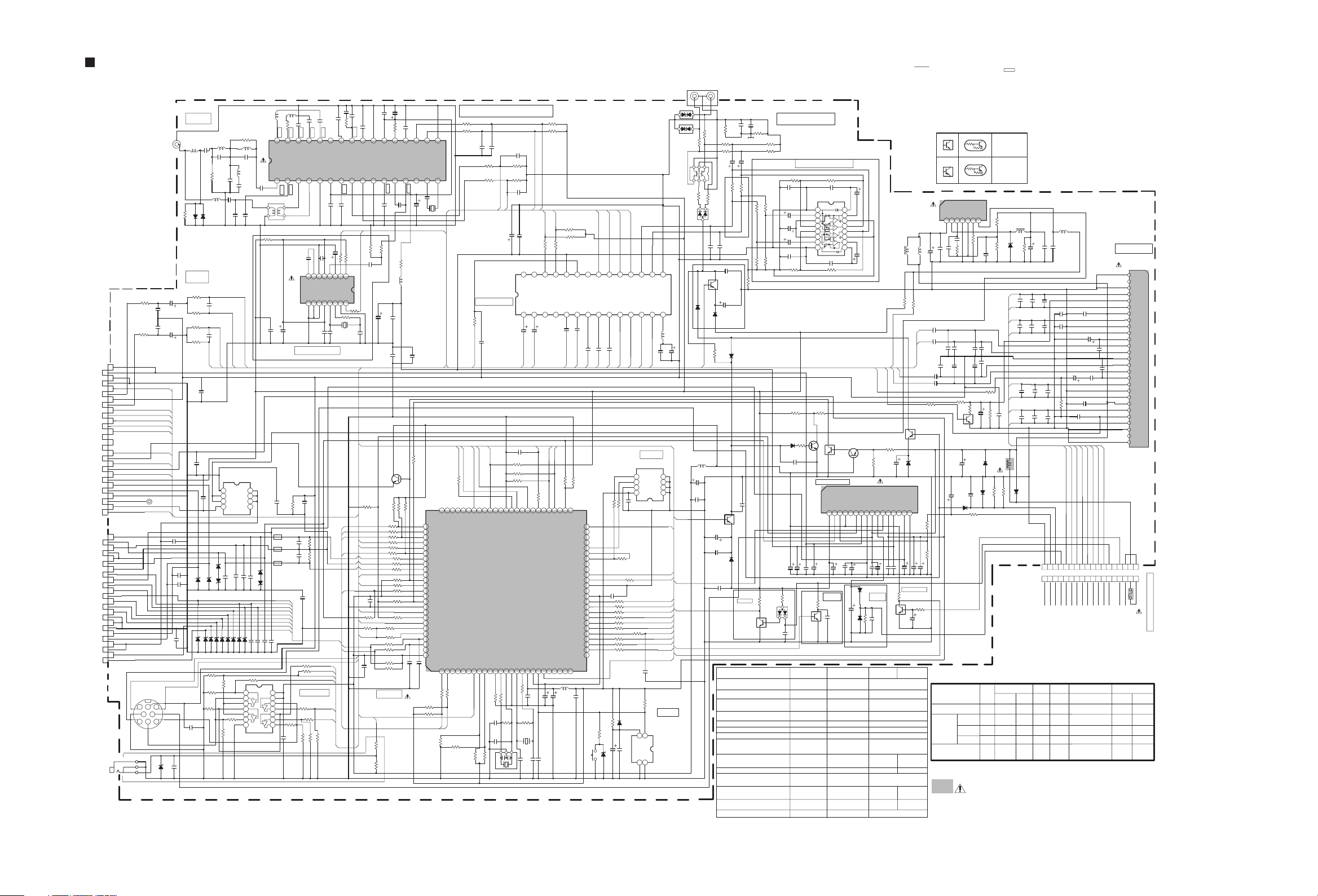
Main section
QTE1H64-225Z
R584
15k
C584
3300p
C583
3300p
R583
15k
QTE1H64-225Z
1
CD_8V
2
GND
3
MGND
4
5
LEFT
6
AGND
7
RIGHT
8
I
9
O
10
UCS
11
SCS
12
CLK
13
BCLK
(NC)
14
(NC)
LRCK
15
SRDATA
(NC)
16
17
PS2A
18
19
3.3V
20
21
SW5V
CN101
To CD section
22
USB-D-
23
USB-D+
24
USBGND
25
26
USBNPP
27
28
CN501
QGB2027ME-28
CN701
QGZ1101J1-24
DETACH CONNECTOR
AUX-L
1
AUX-R
2
AUX-G
3
4
5
ACC5V
6
GND
7
VOL1
8
10V
9
VOL2
10
REMOCON
11
RGBCL
12
LCDCL
13
LCDCE
14
LCDDA
15
USBGND
16
section CJ601
To LCD & Key control
17
18
USB-D+
19
USB-D-
20
USB5V
21
22
KEY0
23
KEY1
24
CN703
*
QNS0283-001
QNZ0095-001
CHANGER CONTROL
J801
6 5 4
8
23
JBUS-SCK
3
2
1
CD4_UCS
CD4_CLK
TSUBUYAKI
7
1
D711
*
SW1
CD4_SO
CD4_SI
SCS
LRMUTE
NRST
NPWDOWN
USB_IN
C417
SI/SO
UDZW6.2B-X
J1
QNB0190-001
C586
2.2/50
C585
2.2/50
10
( )
C419
C418
( )
C994
CH.R
CH.L
A-GND
MEMORY.IN
C710
100P
*
27p
27p
100p
R1
FM/AM
TUNER
L8
4.7u
( )
D1
CD
L.P.F.
R588
R587
D719,D720:
UDZW5.1B-X
C802
NI
( )
1SS355W-X
R586
1k
18k
18k
R585
1k
C401
D719
D701
C991
D701-D709:
C1
0.001
L3
QQL213M-R22Z
( )
D2
1SS355W-X
C588
C587
NI
( )
82p
100p
C402
D720
( )
( )
D702
D703
6.8k
R803
R802
100K
R807
100K
L1
C2
820k
R2
0.22u
CD-USB.R
5.3V
5.3V
3.3V
( )
0.47u
5.6p
330p
330p
0V
D716
D715
D715-D718:
( )
D704
100p
C34
( )
C5
15p
22P
CD-USB.RO
HI-SIDE SWITCH
IC401
TPS2051BD-X
GND
1234
IN
IN
CTRL
56p
C734
( )
( )
D706
D705
D707
UDZW6.2B-X
3.9k
R804
R808
100
R819
47k
0
R3
L2
( )
0.47u
C32
( )
5.6p
L31
0.47u
( )
C3
C33
100p
( )
0.001
0.22
C6
C4
CD-USB.LO
CD-USB.L
5.3V
OUT
5.3V
OUT
5.3V
OUT
5 6 7 8
FLAG
0V
1
1200p
56p
D718
C728
C732
D717
C735
UDZW5.1B-X
( )
( )
( )
( )
( )
D709
390p
390p
C726
C727
D708
1K
R801
3.3V
1234567
0V
0V
0V
0V
0V
0V
GND
IC801
74AHCT126PW-X
0.01
1.5V
AMSELIN2
FMRFIN1
2.4V
0V
0.22
47k
47k
1K
0
1K
0.1
C16
0.01
C12
0.01
2.2V
0V
0V
1.5V
PLL2
PLLREF
AMSELIN1
GNDRF
AMRFAGC
VCC
0V
2.5V
8.6V
C13
C25
0.01
RDSDA
2.2k
C73
10/25
C78
R73
*
0V
0V
4.8V
2.4V
2.0V
MUX
CIN
Vdd
GND
Vref
DATA
Vdd
OSCI
TEST
GND
T57
OSCO
0V
0V
2.4V
2.4V
4.8V
X71
C76
0.01
QAX0926-001Z
C75
33p
*
AUX.L
AUX.G
AUX.R
BUSIO
BUSINT
BUSCLK
/BUSIO
0.01
C17
C18
0.1
C19
4.7K
4.5V
3.3V
R4
5.6V
PLL1
VCO
IC1
TEF6606T/V3-X
ROUT
LOUT
3.8V
3.8V
2.1V
1
NI
RDSCL
R75
C72
( )
0V
12345678
QUAL
CLK
R72
2.2K
2.4V
R71
0
C74
33p
R757
LCDDA
LCDCE
LCDCL
VOL_SDA
VOL_CLK
RGBCL
TUSDA
RDSDA
TUSCL
STEERING
RDSCL
REMOCON
C708
0.1
MUTE
R750
SUB-MUTE
R760
1.2k
MODE 2
KEY0
KEY1
C709
R13
0.1
0V
GNDRF
AGND
0V
NI
( )
330p
1.2k
100K
C24
0.01
8.6V
VCC
AMIFAGC2
0.4V
C14
R12 0
( )
C30
220/10
2SC1623A/5-6/-X
R736
560
R737
560
R738
560
R739
100
R741
100
R740
560
R742
100
R743
100
R744
100
R746
100K
R745
270
R747
10K
R748
1.2k
R727
1.2k
R761
1.2k
R762
1.2k
R752
4.7K
R753
4.7K
R755
4.7k
R756
4.7k
C26
100/16
C23
22
R5
3.9V
7.3V
VREG
MPXIN
3.6V
3.7V
3.6V
C15
0.22
0.1
R11
L7
4.7u
( )
C31
0.1
C990
( )
1800p
5.1V
0V
0V
Q978
R766
4.7k
4.7k
R768
R765
*
*
CPU
*
*
R770
*
R773
IC701
STEERING
2.2k
22k
BUSSI
BUSSO
6.8K
R811
L6
L5
560u
560u
1
C10
C11
0
R10
4.0V
7.0V
0V
8.6V
1.4V
7.0V
8.6V
AMIFAGC1
AMSELOUT2
AMSELOUT1
FMRFIN2
AMRFIN
AMRFDEC
1 2 3 4 5 6 7 8 9 10 11 12 13 14 15 16
0V
0V
3.1V
4.2V
3.1V
2.6V
L4
QQR1813-001
R74
100
C71
560p
2.4V
SCOUT
IC71
MODE
LC72725KM-X
9 10 11 12 13 14 15 16
0V
C79
0.01
( )
C77
47/6.3
RDS DETECTOR
C733
( )
100p
C731
( )
R734
470
K161
NRSA02J-0R0X
C730
C714
Vdd
K162
NRSA02J-0R0X
K163
NRSA02J-0R0X
0.1
0.1
C715
8 9 10 11 12 13 14
RGBCL
REMOCON
LCDDA
5V
5V
0V
0V
0V
0V
LCDCL
LCDCE
R733
3900p
R732
3900p
C729
C992
22p
VOL1
VOL2
KEY0
KEY1
R806
R805
JVC BUS
R810
3.9K
R813
R814
100
47k
100K
C801
0.047
R809
R812
VREF
MPXOUT
4.7
4.7k
NI
TUNER SECTION
R6
0.1
5.1V
5.1V
SCL
SDA
TEST
RSSI
6.3V
4.0V
3.3V
C22
15p
C27
10/25
QAX0928-001Z
100
100
R7
0V
17181920212223242526272829303132
GND
100P
C29
100P
C28
( )
DGND
XTAL
6.3V
X1
( )
R91
*
R81
*
IC161
TDA7718-X
TU.L
E.VOLUME
0
NI
R164
( )
NI
0.01
C185
( )
C993
( )
1800p
R749 1K
75 74 73 72 71 70 69 68 67 66 65 64 63 62 61 60 59 58 57 56 55 54 53 52 51
0V
LCD_DATA
76
0.2V
77
LCD_CE
0.2V
78
LCD_CLK
5V
79
EVOL_SDA
5V
80
EVOL_CLK
5V
RGB_CLK
81
5V
82
TU_SDA
2.4V
83
RDS_DATA
5V
84
TU_CLK
0V
85
STEERING_REMOTE
0V
86
PS2
2.5V
87
RDS_CLK
5V
88
REMOCON
5V
89
VDD5
***
90
POWER
0V
91
VSS
5.0V
MUTE
92
***
93
CD_ON
0V
SUB-MUTE
94
***
95
ILL
***
96
AUTO_ANT
5V
97
KEY0
5V
98
KEY1
NC
99
5V
100
VREF+
( )
( )
C723 NI
100P
C724
100P
R701
10k
R704
100K
R703
100K
VOL1
R709
*
VOLMUTE
SCS
SW1
USB_IN
LRMUTE
AMPKILL
( )
1K
R730
3.2V
0V
NC
NC
NC
NC
NC
NC
NC
SW1
SW2
PSW
MOTOR_SEL
VOL2
VOL1
BUZZER
I2C-REQ
I2C-DATA
I2C-CLK
MMODNCSTAGE2
USB-RST
STAGE1
NC
0V
3.3V
3.3V
10k
R702
VOL2
47k
R711
47k
1.6V
0V
0V
3.3V
47k
BEEP
R767
R712
( )
( )
C701
27p
( )
27p
( )
X701
*
R708
R710
100k
100K
QAX0667-001Z
R14
4.7k
4.7k
R15
C92
0.01
( )
R92
*
R82
*
( )
0.01
C82
TUSCL
TU.R
R729
100K
R763
82K
0V
LM
VSS
OSC1
OSC2
1.6V
330
R713
C702
TUSDA
R161
4.7k
LROUT
R162
9.0V
VDD
TUNER
SE3L
3.2V
1
C161
TU.L
27K
3.3V
NC
PS1NC
E2PROM_CLK
E2PROM_DO
E2PROM_DI
NPWDOWN
CD4_CLK
CD4_SI
CD4_SO
BUSCLK
BUSSI
BUSSO
CD4_UCS
BUSINT
/BUSIO
BUSIO
NC
25242322212019181716151413121110987654321
SSTOP
VDD18
LFOUT
4.7k
3.9V
3.9V
3.2V
MUTE
WINTC
OUTLF
OUTLR
QD3R
QD3G
QD3L
SE3R
3.2V
3.2V
3.2V
3.2V
1
C171
1
1
1
C165
C174
C164
AUX.G
AUX.R
TU.R
AUX.L
47k
R758
270
R771
0V
50
NC
49
48
AFS
47
ROM
3.3V
46
3.3V
45
3.3V
44
43
NC
42
NC
3.3V
41
3.3V
NRST
40
0V
39
VSS
38
MLD
C720
82p
1.8V
37
3.3V
36
3.3V
35
3.3V
34
33
0V
32
0V
31
0V
30
0V
29
3.3V
28
27
26
S701
QSW0648-001Z
C721
0.1
R724
R725
0V
R723
R722
R721
R719
R718
R717
2.2k
R775
100
R779
47/6.3
C711
T
( )
D713
UDZW5.6B-X
VOL_CLK
VOL_SDA
220/10
1.0
C183
C184
100
100
R172
R171
0.2V
5.1V
SCL
SDA
WIN_IN
DC_ERR
CD/USB
CD-CH
SE2R
SE2L0VSE1R
SE1L
1 2 3 4 5 6 7 8 9 10 11 12 13 14
3.2V
3.2V
1/50
1/50
C172
C162
QTE1H57-105Z
QTE1H57-105Z
CH.L
CH.R
C716 NI
( )
VOLMUTE
DIMIN
LRMUTE
R714
( )
TELMUTE
R726
NI
R759
( )
3.3V
0V
0V
0V
0V
NC
NC
NC
NC
DIM_IN
USB_IN
VOLMUTE
TEL_MUTE
NC
DCDC-SWREG
RST
XO
VDD18
VDD33NCXI
NC
1.8V
3.3V
1.7V
3.3V
3.3V
0
R715
20p
C704
C717
820p
X702
QAX0401-001
20p
C703
L702
4.7u
C719
100/10
C722
4.7/25
0.1
C718
( )
R764 82K
3.3V
3.3V
SCS
VSS
0V
1.6V
RROUT
3.9V
3.2V
CD-USB.L
270
R772
R777
10K
( )
C712
OUTRR
SE4L
*
3.3V
0V
3.3V
R731
100
1K
R728
1K
1K
1K
1K
1K
R720
1K
1K
1K
D712
1SS355W-X
0.01
RFOUT
3.9V
OUTRF
SE4L0
3.2V
CD-USB.LO
IC771
0V
C771
0.047
3.9V
OUTSW/OUTLR2
SE4R0
3.2V
CD-USB.RO
EPROM
5678
SDA
SCL
Vdd
1K
C741
( )
3.3V
2 1
RST
VDD
NC
GND
43
0.0V
0.0V
3.9V
OUTSW/OUTRR2
SE4R
3.2V
CD-USB.R
GND
56p
R774
47k
3.3V
L161
56p
C177
A1A2WPIN
A0
DOMMUTE
NPWDOWN
CD4_CLK
CD4_SI
CD4_SO
BUSCLK
BUSSI
BUSSO
CD4_UCS
BUSINT
/BUSIO
BUSIO
RESET
IC702
D352
NAF0029-001X
( )
D342
( )
NAF0029-001X
Q331
IMX9-W
0V
1516171819202122232425262728
GNDCREF
3.2V
0.027u
NQL553J-27NX
C178
10/16
QTE1C57-106Z
0V
1 2 3 4
MUTE
( )
NRST
MODE 2
TELMUTE
DOMMUTE
DIMIN
SWREG
S-80824CNNB-G-W
REAR/SUBWOOFER R
100
R343
0V
0V
65
4
3 2 1
0V
0V
2.2k
R341
5V
1SS380-X
D786
SUB-MUTE
L701
4.7u
C707
100/16
C706
820p
( )
REAR/SUBWOOFER L
R353
100
0V
0V
2.2k
R351
-
D331
MC2836-X
56p
C166
C786
0V
5V
R784
4.8V
C781
100/6.3
( )
C787
0.01
( )
C705
0.01
1. RDS: IC71, X71
11. TEL-MUTE
13. J321
*
J321
C341
0
NI
B12
R352
820
R342
820
C381
4.7/50
0
*
*
R389
56p
C176
NI
( )
0.082
Q785
RT1P141C-X
C785
100/6.3
NOT
USED
D787
1SS355W-X
0
D785
1SS355W-X
0V
4.9V
D781
1SS355W-X
*
REMARKS
*
R12, R743, R745
R71-R74, C71-C78
2. C78
3. AUTO ANTENNA
C851, C852, R851
D851, D852
4. R81 & R91
R82 & R92
5. EEPROM IC771
6. POWER CORD
7. D902
8. STAGE SETTINGS
R708
R709
9. 5V LINE OUT AMP
IC381, R381 - R388
C383 - C390, C392
10. R389, R390
Q891, D891, C891
R891, R892
12. OE REMOTE
CN703, D711, C710
R770, R773
(LINE OUT PIN JACK)
14. MICON IC701
( )
C382
R390
C782
Q781
RT1P141C-X
TELMUTE
(STAGE 1)
NOTES
1. VOLTAGES ARE DC-MEASURED WITH A DIGITAL VOLT METER WITHOUT INPUT SIGNAL
CONDITION---FM MODE. AM MODE. ( )CD MODE.
UNLESS OTHERWISE SPECIFIED.2.
ALL RESISTORS ARE 1/16W 5% METAL GLAZE RESISTOR.
ALL CAPACITORS ARE 50V OR 25V CERAMIC CAPACITOR.
ALL RESISTANCE VALUES ARE IN OHM.
ALL CAPACITANCE VALUES ARE IN uF(P=pF)
ALL E.CAPACITORS ARE SHOWN IN THE FORM OF CAPACITANCE(uF)/RATED VOLTAGE(V)
COMPONENTS IN () INDICATE NOT USE.
3.
REAR/SUBWOOFER
LINE OUTPUT
C321
NI
( )
0.022
0
B8
R354 47k
R344
47k
*
4.2V
1SS355W-X
Q891
D782
D891
MC2836-X
R386
C386
4.7/50
C392
10/16
4.7/50
C385
R385
C783
( )
0.01
NI
C908
220/10
R891
1k
-
C891
0.1
5V LINE OUT AMP
22K
0.1
9.0V
C384
3.1V
4.7V
3.1V
3.1V
4.7V
C383
3.1V
9.0V
0.1
22K
R781
47K
5.1V
0V
R782
4.7k
0V
C906
0.01
C907
220/10
Q892
RT1N141C-X
R388
C388
*
IC381
NJM2160BV-X
12345678
C387
R387
R783
10K
Q976
RT1N141C-X
0V
Q782
0V
2SC1623A/5-6/-X
REGULATOR
SW5V
5.1V
C913
C905
47/16
FOR
DOMESTIC
3.3K
R893
C892
0.1
NOT
USED
33K
0.0015
0.0015
33K
ACC5V
5.1V
4.4V
10/25
( )
8.3V
0.8V
0V
7.8V
7.8V
0V
0.8V
8.3V
9 10 11 12 13 14 15 16
Q977
2SA812A/5-6/-X
4.9V
5.1V
VDD5V
ACC.IN
5.1V
C911
0.1
C910
( )
C851
10/25
C390
100/16
10u
4.7u
LFOUT
IC901
47K
ILM.ADJ
C912
0V
( )
QQL92AK-100Z
L930
47k
R938
( )
R930
QFV91HJ-474Z
QFV91HJ-474Z
0V
RT1P141C-X
11.1V
C784
100/16
GND
ILM.10V
16151413121110987654321
0V
10.2V
C903
100/16
0.01
DIMMER INPUT
Q881
RT1N141C-X
9.6V
C881
22/16
D784
C917
( )
0
13.6V
Q784
UDZW11B-X
330/6.3
L933
NQLH25M-4R7X
RROUT
C301
QFV91HJ-474Z
RFOUT
C302
QFV91HJ-474Z
C312
C311
( )
R902
9.1k
(1/10W)
C909
330/6.3
R903
R882
4.7K
470/25
C931
C348
56p
R308
270
4.7k
100/16
C389
SWREG
BEEP
LROUT
AMPKILL
( )
R977
12k
5.7V
(1/10W)
R976
27k
(1/10W)
AN34002A
CD8V
MODE 1
NC
D852
**
10/25
CRS03-W
3.3V
ANT
MEMORY IN
EXT
9V
MODE 2
**
0V
8.1V
3.3V
9.2V
13.7V
14.4V
C914
C915
C916
0.01
0.1
100/16
( )
D851
AUTO
ANTENNA
R881
MA22F20-X
*
0V
R851
4.7k
0.22
C852
4.7/50
0
1K
1K
R382
R381
100K
100K
R384
R383
0
B176
( )
0.082
47k
R892
0V
RT1N141C-X
0V
IC931
QEZ0595-477Z
0.47
0.47
C345
56p
0.47
0.47
(1/10W)
BD9007HFP-W
SW
VIN
5.3V
14.4V
18p
C928
2.2
R928
C940
C938
C347
56p
R305
RT1N141C-X
C901
C902
2.2/50
MA22F20-X
10K
10K
UN2211
RT1N141C-X
10K
UN2111
RT1P141C-X
10K
DC-DC 5V USB SUPPLY
FB
RT
EN
INV
GND
7654321
0V
0V
0.8V
3.3V
0.6V
51k
4700p
75k
R929
C304
C303
C346
100p
100p
( )
56p
C313
100p
( )
R310
1K
1K
R306
( )
C316
( )
Q301
QEZ0869-278
2700/16
D901
1N5401-F64
0.1
C971
D971
D972
CRS03-W
R901
1k
(1/4W)
L931
82k
R940
QQL92AK-330Z
33u
1/8W
15k
D931
R939
C939
150p
RSX201L-30-X
( )
R971
3.3K
C324
27k
(1/8W)
0.01
L901
( )
R972
2.2K
QQR1852-001
(1/8W)
R937
FR-
82p
( )
C329
FR+
RR-
82p
C334
( )
C330
RR+
RL+
82p
( )
C331
RL-
FL+
82p
( )
C328
FL-
D902
*
CN901
QNZ0607-001
( )
( )
C314
100p
( )
4.7k
R307
4.7/50
220
C932
330/6.3
QBZ0006-337Z
82p
82p
C337
C333
( )
82p
82p
C338
( )
82p
C339
C335
( )
82p
C336
C332
( )
L932
NQR0007-002X
1500p
4.7
C937
C933
( )
C323
0.01
C322
( )
0.01
QTE1C57-476Z
O
C326
NCB21AK-225-A
22/16
82p
( )
10
R309
C315
82p
( )
RR+
RR-
RL-
123456789
ANT
ACC
GND
*
REMOTE
REAR LEFT(-)
REAR RIGHT(-)
REAR RIGHT(+)
C320
0.022
C317
47/16
C340
82p
C325
82p
( )
2.2
C318
C319
0.022
1
FL+
FL-
FR-
FR+
RL+
101112131415161718
987654321
REAR LEFT(+)
FRONT LEFT(-)
FRONT LEFT(+)
FRONT RIGHT(-)
FRONT RIGHT(+)
POWER AMP.
4.6V
7.1V
14.4V
7.1V
7.1V
8.3V
6.8V
6.8V
6.8V
6.9V
6.9V
7.1V
7.1V
14.4V
7.1V
5.1V
7.1V
TELMUTE
*
IC301
TDA7851A
0V
0V
7.1V
0V
0V
0V
0V
0V
MEMORY
ILLUMINATION
TAB
OFFSET
DETECT
GND
OUTFR-
STBY
OUTFR+
VCC1/2
OUTRR-
GND
OUTRR+
RIPPLE
INRR
INFR
PRE-GND
INFL
INRL
AC-GND
OUTRL+
GND
OUTRL-
VCC3/4
OUTFL+
MUTE
OUTFL-
GND
CD
TAB
27 26 25 24 23 22 21 20 19 18 17 16 15 14 13 12 11 10 9 8 7 6 5 4 3 2 1
181716151413121110
FUSE 15A
*
QMFZ064-150-J1
POWER CORD ASS'Y
To SPK BATTERY
KD-601E
USED
NCB31HK-122X
NOT USED
6.8k
S-24CS16AOI-G-X
QAM1150
GS1J-X
(LOW)
NOT USED
USED
NOT USED
USED
USED
USED
QNN0802-001
MN101E16YFF
KD-R604UI
KD-R605U
NOT USED
NDC31HJ-821X
S-24CS04AFJ-G-X
QAM1146-001
-001
NOT USED
NOT USED
NOT USED
USED
NOT USED
NOT USED
NOT USED
QNN0802-001
KD-R606U
USED
6.8k
6.8k6.8k
(LOW)
USED
MN101E16YFE
QNN0802
KD-R600J
S-24CS04AFJ-G-X
NOT USED
USEDUSED
NOT USED
USED
MN101E16YFE
NOT USED
NDC31HJ-821X
NOT USED
QAM1143-001
NOT USED
(HIGH)
NOT USED
NOT USED
-001
15k
8.2k
USED
** Regulator Pin Voltage
KD-A605J
*** POWER, CD_ON, ILLUMINATION and AUTO ANTENNA
OPERATION
1. Power OFF
2. Power ON
Tuner Mode
CD Mode
Aux Mode
3. STBY
(CLK DISP ON)
USED
NOT
USED
MAIN PWB: GEB10260A
Parts are safety assurance parts.
When replacing those parts make
sure to use the specified one.
QNN0832
USED
USED
-001
MODE 1
3.2V
0V
3.2V
3.2V
0V
( MODE 1 and MODE 2 )
MODE 2
J,E
Version
Version
0V
1.6V
1.6V
1.6V
1.6V 1.6V
POWER
CD_ON
ILLUMINATION
J,E,U
U
J,E,U
Version
0V
0V
4.9V
3.2V
1.6V
4.9V
4.9V
1.6V
0V
Version
J,E,U
0V
4.8V
4.9V
4.8V
4.9V
4.9V
4.8V
4.8V
0V
AUTO ANTENNA
U
J,E
Version
0V
Version
Version
0V
0V
0V
4.9V
0V
0V
0V0V
0V
0V
2-5
Page 79

LCD & Key control sectionion
SW
Tr
QNZ1006-001
CN603
VCC
1
D-
USB
2
D+
3
GND
4
10
C655
15K
15K
( )
NI
R6040
NCJ11EK-106X-R
S612
COLOR
R613
10K
D616
UDZW5.1B-X
( )
UDZW5.1B-X
D617
NI
R6041
SELECT
R605
R606
3.9K
2.7K
S605 S604 S603 S602
UP F-SKIP
R612
R607
3.9K
S611
R611
1.8K
2.7K
S610
EQ/TP/PTY
5
6
R6044
0
L602
NQR0536-001X
R6043
0
ENCODER
54
JS686
QSW1263-001
R604
R603
1.2K
1.8K
B-SKIP
R610
1.2K
S609 S607
321
B
A
DOWN
S608
BACKDISP
PWB:
P
C601
0.022
( )
R602
820
R609
820
GEB10261A1
C602
( )
0.022
KEY MATRIC
R601
820
S601
POWER/ATT
R608
820
MENUEJECT
S606
SRC
USB-D-
USB-D+
S41
S42
S43
S44
S45
S46
S47
S48
S49
S51
S50
COM4
COM3
COM2
COM1
LCD DISPLAY
CLASSIC
CH
TAG
1
S3
S2
VOL2
VOL1
270
R630
KEY0
DISC
S13
S12
S11
S10S9S8S7S6S5S4
LCD1
- - 40 41 42 43 44 45 46 47 48 49 50 51 52 53
S21
S20
S22
S19
S18
S17
S16
S15
S14
HIPHOP
RND
REG
AF
S32
S31
S29
S30
S28
S27
S26
S25
S24
S23
POWER
KEY1
C603
0.1
( )
( )
D630
NI
D606
LHQ974/LM/-X
54
JAZZ
S33
S35
S34
S36
LCD1
QLD0578-001
ROCK
RPT
TP
39383736353433323130292827262524232221201918171615141312111098765432
S40
S38
S39
S37
(1/8W)
R631
470
EQ/ TP/PTY
D632
LHQ974/LM/-X
( )
NI
R633
EJECT
680
R634
R632
( )
D631
NI
LHQ974/LM/-X
0V
0V
HOLD
DIM
5V
5.66V
C607
1
( )
4.9V
0.1
C650
Q602
UNR9211G-X
POPS
STMOPTY
Q601
10V
2SC5845-X
1K
R651
390K
R660
D650
C661
1
UDZW5.6B-X
USER
HD
R661
1K
C663
0.022
D661
1SS355W-X
EQ
CJ601
QGZ1101K1-24
AUX-L
AUX-R
AUX-G
ACC5V
DGND
VOL1
10V
VOL2
REMOCON
LCDCL
LCDCE
LCDDA
USBGND
USBGND
USBGND
USB-D+
USB-D-
USB5V
USB5V
KEY0
KEY1
D668
MA8062/M/-X
( )
NAF0029-001X
D669
J601
QNS0215-001
2
1
3
AUX JACK
1
2
3
4
5
6
7
8
9
10
11
12
13
14
15
16
17
CN701
To Main section
18
19
20
21
22
23
24
LOUD
REMOCON
R670
IC681
NJL29H380A
VDD5VGNDOUT
321
0V
5V
D681
C682
UDZW5.1B-X
( )
0.1
C681
( )
R682
S50
S49
S51
COM2
COM1
COM4
COM3
2.5V
49
2.5V
50
2.5V
51
2.5V
52
2.5V
53
2.5V
54
2.5V
55
5.0V
R662
1K
C665
0.1
VDD1
VDD2
OSC
1K
R663
INH
R665
LCDCE
R666
LCDCL
R664
220K
0.1
C666
C662
150P
LCDDA
R667
56
3.3V
57
1.7V
58
0V
59
1.6V
60
4.8V
61
0.1V
100
CE
62
5.1V
100
CLK
63
2.4V
100
DATA
64
4.7/6.3
1K
R683
( )
NI
S48
S47
S46
S45
S44
2.5V
2.5V
2.5V
2.5V
2.5V
48 47 46 45 44 43 42 41 40 39 38 37 36 35 34 33
470
R681
S41
S40
S39
S38
S36
S43
S42
2.5V
2.5V
2.5V
S35
S37
2.5V
2.5V
2.5V
2.5V
2.5V
2.5V
LCD DRIVER
IC661
PTC6526LQ-L
2.5V
2.5V
2.5V
2.5V
2.5V
2.5V
2.5V
2.5V
2.5V
2.5V
2.5V
2.5V
2.5V
4.9V
DIM
S2
S5S4S3
S6
S13
S12
S11
S10S9S8
S7
D659
D660
( )
( )
MA8062/M/-X
NAF0029-001X
S34
S33
2.5V
2.5V
2.5V
S32
32
S31
2.5V
31
S30
2.5V
30
S29
2.5V
29
S28
2.5V
28
2.5V
S27
27
S26
2.5V
26
S25
2.5V
25
S24
2.5V
24
2.5V
S23
23
2.5V
S22
22
S21
2.5V
21
S20
2.5V
20
S19
2.5V
19
S18
2.5V
18
2.5V
S17
17
16151413121110987654321
2.5V
2.5V
S14
S16
S15
R671
10K
10K
C685
C684
0.001
0.001
C686
( )
0.001
K670
K672
K671
NQR0007-002X
NQR0007-002X
NQR0007-002X
100
NAF0029-001X
( )
D664
R672
MA8062/M/-X
( )
D665
100
D666
NAF0029-001X
( )
( )
D667
MA8062/M/-X
( )
R673
T1-1
T2-1
10V
10V
6
5
4 3
D603
NSSM065T-X
:
NSW0124-001X
S601
R644 1.2K
R645
R646 1.6K
R647
R648
R649
GEB10261A2
NSW0316-001X
1.2K
910
910
1.2K
T1-2
T1-3
T1-4
L601
NI
( )
R652
0
C651
10/16
C606
( )
0.22
IC
1234567
IC
2.2K
R636
0V
5.0V
5.0V
0V
5.0V
2SA2174G-X
4.4V
Q607
0V
Q605
UN2222-x
( )
0.22
C610
Q608
UN2222-X
R656
(1/8W)
330
T2-2
R657
(1/8W)
330
T2-3
R658
(1/8W)
620
T2-4
2.2K
R637
5.0V
4.4V
5.0V
5.0V
0V
C609
0.22
Q604
2SA2174G-X
2.2K
R638
5.0V
4.4V
5.0V
( )
Q610
C608
2SA2174G-X
0V
5.0V
Q611
0V
UN2222-X
0V
4.4V
4.4V
4.4V
0V
0.22
( )
IC601
NCP5623DTBR2G-X
GND
B-LED
G-LED
R-LED
NC
141312111098
5.0V
Vbat
R626
Vout
5.0V
0V
SCL
0.6V
R614
IREF
2.6V
R615
SDAAGND
100
NC
1
C604
0
C605
1
( )
R616
4.7K
( )
R618
100
1%
150K
S602-S612
6
1
5
2
4 3
D601
NSSM065T-X
6
1
5
2
4 3
D605
NSSM065T-X
1
6
1
2
5
2
4 3
D604
NSSM065T-X
LCDDA
RGBCL
D611
( )
UDZW5.1B-X
NOTES
4.7K
UN2222-X
4.7K
10K
UNR9211G-X
10K
1. VOLTAGES ARE DC-MEASURED WITH A DIGITAL VOLT METER WITHOUT INPUT SIGNAL
UNLESS OTHERWISE SPECIFIED.2.
ALL RESISTORS ARE 1/16W +5% METAL GLAZE RESISTOR.
ALL CAPACITORS ARE 50V OR 25V CERAMIC CAPACITOR.
ALL RESISTANCE VALUES ARE IN OHM.
ALL CAPACITANCE VALUES ARE IN uF(P=pF)
ALL E.CAPACITORS ARE SHOWN IN THE FORM OF CAPACITANCE(uF)/RATED VOLTAGE(V)
T --- TANTAL CAPACITOR.
COMPONENTS IN ( ) INDICATE NOT USE.3.
2-6
Page 80
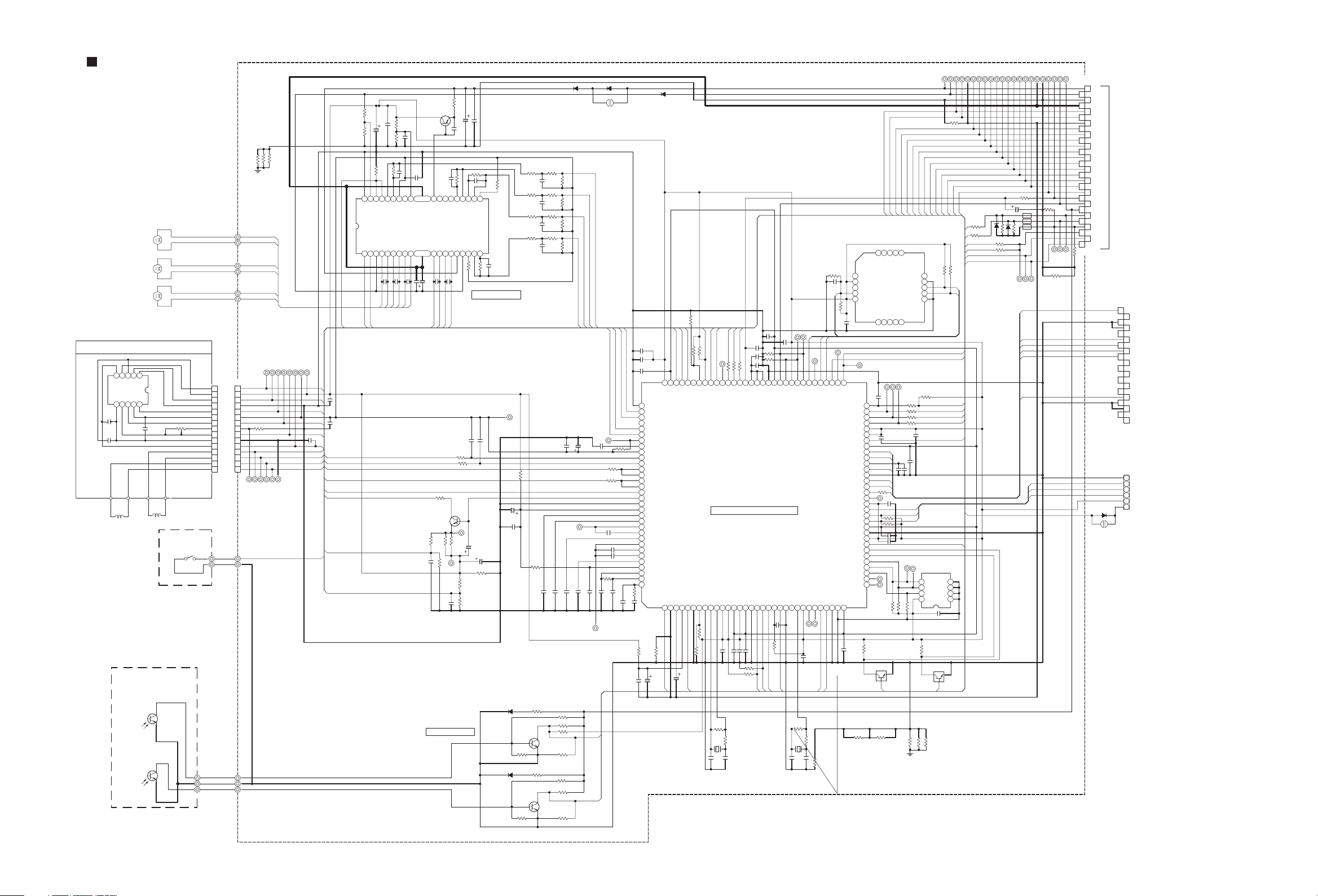
CD section
+
SPINDLE
MOTOR
-
+
FEED
MOTOR
-
+
LOAD
MOTOR
-
A'SSYPICKUP
OPTIMA-727A1
5 4 3 2 1
HDU-120
109876
1
FOCUSING COILTRACKING COIL
PHOTO PWB
LVB10787-A2
Q212
PS1191RB22/BC/X
Q211
PS1191RB22/BC/X
0.1
REST SW PWB
LVB10787-A3
0.1
1k
NSW0291-001X
TRACKING+
TRACKING-
SW1
SW2
GND
SW1
FOCUS-
FOCUS+
D503
1SR154-400-X
Q501
2SB1424/R/-W
1/2W
0.1
R501 10
33k
R505
68k
R506
C531 100/6.3
R14 NI
R15 NI
R16 NI
FG2
M.G
SP+
SP-
FEED+
FEED-
LOAD+
LOAD-
MUTE
VCC
LD
VF1
VT2
VC
MD
VT1
VF2
CN102
QGF0522F3-15W
VF2
Vcc
VT2
GND
VT1
Vc
VF1
VR
MD
GND
LD
1.9V
1
1
3.3V
2
2
2.0V
3
3
0.0V
4
4
2.0V
5
5
1.6V
6
6
1.9V
7
7
R331
0.0V
8
8
150
0.1V
9
9
0.0V
10
10
1.8V
11
11
3.4V
12
12
3.1V
13
13
3.3V
14
14
3.2V
15
15
FCS+
TRK-
VR
FCS-
TRK+
RFGND1
C103
VF2
VT2
VT1
VF1
0.1
FOCUS-
FOCUS+
0.1
C101
0.1
C102
MD
LD
VT2
VT1
TRK+
TRK-
VF1
VF2
MD
LD
CDLDCUR
PSW
CUR3.3V
R525
4.8V
3.2V
36
35
34
S-GND
MUTE1
VCONT
7.2V
0.0V
0.0V 0.0V
FWD
REV
C504
47k
33
NI
LOAD-
3.2V
0.0V
C532 0.1
1.6V
32
MUTE234
0.0V
LOAD+
R503
R504
R519 8.2k
1.7V
31
VIN4
VIN4-
3.5V
NIC505
SP+
NI
8.2k
C533
5.1k
NI
C519
1.6V
1.6V
1.2V
30
29
28
VREF-IN
REG-OUT
VREF-OUT
IC501
LA6565-X
VO3-8VO3+7VO4-6VO4+5VLO+4VLO-3VCC22REV1FWD
9
3.2V
3.3V
3.1V
NI
C506NIC507NIC508
FEED-
FEED+
SP-
3.3V
68p
C503
0.0V
4.3V
38
27
GND
REG-IN
GND
37
3.4V
0.0V
NI
C551 100/10
C552
FOCUS-
R319
ISA1530AC1/RS/X
R345
4.7k
0.1
R346
C337
PHOTO SWITCH
1.4V
26
VIN+OP
3.1V
FOCUS+
Q301
25
5.0V
4.3V
1.5V
VIN-OP
3.2V
TRK-
0
1.8V
3.0V
NI
C336
C520 NI
7.1V
24
VO-OP
3.3V
TRK+
R322 8.2K
R323 8.2K
R326 10
LD+
0.1
C501 47/25C316
C535 NI
R520
8.2k
1.6V
1.6V
23
22
VIN3
VIN3-
7.2V
6.3V
2.3V
LD-
R325 10
R343
4.7k
R344
NI
C502
R521 8.2k
NI
C521
1.7V
1.6V
1.6V
21
20
19
VIN2
VIN2-
VIN2+
VIN117VIN1-16VIN1+15VCCS14VCCP113VO1+12VO1-11VO2-10VO2+
18
1.6V
1.6V
1.6V
R522
8.2k
8.2k
R524
CD DRIVER
C321 2700p
C320 NI
47/6.3
C315
47/6.3
R317
47k
R523
8.2k
C522 NI
VREF
C318
C371
D201
AN1105W21/AB/-X
D101
AN1105W21/AB/-X
R511 10k
R507
6.8k
R515
C511
6800p
R508
R512 15k
15K
R516
C512
2200p
R509
R513 8.2k
18k
R517
C513
2700p
R510
R514 13k
68k
R518
C514
1200p
C324
0
R371
NI
NI
R316
82k
4.7
3300p
C313
C314
C317 0.022
R201
R203
180k
390
R202
R242
0.1V
Q201
0.6V
2SC3928A/R/-X
2SD601A/R/-X
0.0V
R101
390
0.0V
0.0V
Q101
2SC3928A/R/-X
2SD601A/R/-X
R205
15k
R103
180k
R102
8.2k
R105
18K
R204
180k
0.6V
R104
180k
D502
1SR154-400-X
D501
SPOUT
1SR154-400-X
SW1
OUTL
OOOUTR
SCS
UCS
CLK
I
NRFDET
0.0V
0
static C/M
IPOD 2.0B
NC 20
NC 19
NC 18
NC 17
NC 16
NC
MODE0
I2C_SDA
I2C_SCL
VSS
NC10
NC9
NC8
NC7
NC6
R361 10K
MONI3
MONI4
MONI5
R307 1k
R327
100
R328
100
R329
100
C340
0.1
TRCD3
TRCD2
TRCD1
TRCD0
TRCST
R336
33
EXTRG1
C347
BDO
PS2
B304
C343
TRCCLK
TP002
47k
R207
0.0V
Q302
RT1N441C-X
0.1
C344
0.1
R308
R309
C345 0.1
C346 0.1
47k
R206
0.1
C393
0.1
C394
10/6.3
EXTRG
D32SCLK
100K
D32SDATA
100K
TP001
BR24L16F-W-X
3.3V
5
6
3.3V
7
0.0V
8
47k
3.3V
R241
R337
R11 NI
R12 NI
FG1
IC303
MFI341S2162-X
R245 NI
1
NC
2
MODE1
C202
NI
3
NC
4
nRESET
5
VCC
611R230
10K
CP_RST
NI
R335
REV
FWD
MUTE
C335
0.1
C332
10/6.3
C304
0.1
0.0V
DVSS97
1.5V
SPOUT98
1.6V
TRVP99
0.0V
NC100
1.6V
TRP101
1.5V
FOP102
1.6V
OSCIN103
1.6V
CTRCRS104
1.6V
VREF105
2.0V
E106
2.0V
F107
1.8V
D108
1.8V
B109
1.9V
C110
1.9V
A111
0.1V
PD112
2.3V
LD113
0.0V
AVSS2114
3.3V
AVDD2115
2.1V
CENV116
1.5V
RFENV117
1.1V
RFOUT118
1.7V
RFIN119
1.1V
ARFDC120
1.2V
ARFOUT121
1.1V
ARFFB122
1.6V
ARFIN123
1.6V
DSLF124
1.0V
IREF125
1.4V
PLLF126
1.4V
PLLFO127
0.0V
VCOF128
R314
2.7k
C307
0.33
1000p
R339
R301 10
0.1
47/6.3
C303
C302
47K
R334
0.0V
3.3V
1.2V
3.3V
0.0V
0.0V
0.0V
96
94
93
92NC91
90
REV
FWD
DVDD95MUTE
IOVDD
AVDD14AVREF
AVSS12OUTL
5
3
1
0.0V
1.7V
3.3V
1.7V
0.0V
1.7V
0.0V
NI
47k
R302
OUTR
OUTL
C301
22/6.3
X301
NAX0375-001X
16.9344MHz
I
O
CLK
SCS
UCS
PSW
47k
R324
3.3V
89
PSW
IPOD_SEL
3.3V
87NC86
CE188CE2
3.2V
TP86
0.0V
3.3V
85
C329 0.1
C334 0.1
100
R312
R313 100
R311 100
0.0V
3.3V
3.2V
84
83
I(S2UDT)
O(U2SDT)
CLK(SCLK)
IC301
MN6627946JC
C330
10/6.3
1.2V
1.2V
81
SREGVDD82SREGOUT
79
SRAMVDD180SRAMVDD2
CPU/CD RF & SERVO/DSP
CSEL7TEST06OUTR
DVSS
11X210X19
8
3.3V
3.3V
1.6V
0.0V
1.5V
NIR303
0.1
C305
R332
1M
220
R333
27p
C341
C342
3.3V
3.3V
0.0V
1.2V
3.3V
1.2V
0.1
10/6.3
10/6.3
C325
C306
C326
R318
47K
R310
47K
USBNPP
USBNOC
NAX0367-001X
27p
C339
1.2V
X302
12MHz
0.1
R305
R306 NI
0.0V
78
0.0V
D-
NSTBY_OUT
C392
0.1
NI
1.2V
3.3V
3.3V
3.3V
3.3V
3.3V
77
76
75
74
73
72
DVSS
DVDD
IOVDD
NPWDWM
NSTANDBY
NSTANDBY_OUT
3.3V
1.6V
1.5V
0.0V
0.0V
3.3V
0.1
C395
10R304
D+
R338
NI
R362
27p
C351
NPD_OUT
TP70
CP_RST
3.3V
0.0V
71
70
CP_RST
CP_RDY
NPWDWN_OUT
0.0V
0.0V
FE
TE
10/6.3
C331
220
27p
C352
CP_DA
0.0V
68
CP_DA69CP_CK
3.0V
CDLDCUR
0 B303
CP_CK
0.0V
3.3V
CUR3.3V
static C/M
3.3V
67NC66
USB_IN
0.0V
C201
0.1/16
610
MONI1
0.0V
0.0V
65
TSUBUYAKI
NRST 64
DOUT/BCLK 63
LRCK 62
SRDATA 61
IOVDD 60
VDD3 59
LRMUTE 58
DVDD 57
TRCD3 56
TRCD2 55
VDD18 54
TRCD1 53
DVSS 52
TRCD0 51
TRCST 50
TRCCLK 49
EXTRG1 48
VPPEX 47
EXTRG0 46
DWier32ASCLK 45
DWier32ASDATA 44
DVDD 43
DVSS 42
IOVDD 41
SW2 40
PS2 39
SW1 38
EEPROMCK 37
EEPROMDA 36
EEPROMCS 35
NRFDET 34
BDO 33
DVDD32DVSS31TEST130CUR3.3V29CDLDCUR28TE27FE26IOVDD25MX224MX123DVSS22USBDP21USBAVDD20USBDM19USBNPP18USBNOC17DVSS16DVDD15IOVDD14DVDD13REGON12IOVDD
1.2V
0.0V
0.1
C373
0 B305
static C/M
TUBUYAKI
R330
C338
0.1
3.2V
0.0V
0.0V
0.0V
3.3V
3.3V
0.0V
1.2V
0.0V
0.0V
1.8V
0.0V
0.0V
0.0V
0.0V
0.0V
0.0V
3.3V
0.0V
3.3V
3.3V
1.2V
0.0V
3.3V
0.1V
3.3V
3.3V
3.3V
3.3V
0.0V
0.0V
0.0V
47k
3.3V
SL001
SPOUT
5.6k
TRVP
5.6k
FOP
NI
TRP
NI
TRP
FOP
TRVP
SPOUT
TRP
FOP
TRVP
OSCIN
C322
C323
0.1
0.15
47/6.3
R349
0
R321
0
R320
0
C319 0.33
RF
C327 0.1
C328 680p
R315
820
1000p
0.015
0.1
C309
0.082
C310
C312
C311
C308
ARF
NI
1K
SW2
BCLK
15
14
13
12
11
IC302
SCL
WPIN
VCC
C104 0.1
47k
3.3V
0.0V
R13 NI
LRCK
CP_CK
SRDATA
GND4SDA
SW1
CD5V
LRMUTE
611R229
10K
CP_CK
TSUBUYAKI
A2
A1
A0
0.0V
Q303
RT1N441C-X
CD8V
R340
PS2
611
10K
CP_DACP_DA
USB_IN
NRST
SRDATA
LRMUTE
0.0V
3
0.0V
2
0.0V
1
0.0V
SW1M
OUTL
AGND
OUTRIO
UCS
SCS
CLK
BCLK
LRCK
M.GND
GND
SRDATA
LRMUTE
PS2
NRST
SW5V
NPDOUT
VDD3.3V
CN101
QGB2027L5-28X
7.8V
CD5V1
7.9V
CD8V2
0.0V
GND3
0.0V
M.GND4
0.0V
SW1
5
1.7V
OUTL6
0.0V
AGND
NI
0B301
C333
5
R217
1/8W
30
5
R216
30
USBNOC
TSUBUYAKI
USBNPP
USB_IN
NRST
NI
NI
NI
15k
F
1%
853
D203
R215
D204
1/8W F
1%
R341
611
NI
0
R342
NRST
D-
D+
R228
BCLK
LRCK
SW2
B302
K101
0
626
K102
626
15k
0
611
0
626
K103
R214
853
static C/M
USBNPP
USB_IN
USBNOC
TRCCLK
TRCD0
TRCD1
TRCD2
TRCD3
TRCST
EXTRG
D32SCLK
D32SDATA
7
1.7V
OUTR8
0.0V
I
9
3.3V
10
3.2V
UCS
11
3.2V
SCS
12
3.1V
CLK
13
0.0V
14
BCLK
0.0V
LRCK
15
0.0V
SRDATA
16
0.0V
LRMUTE
17
0.0V
18
PS2
3.1V
NRST
19
3.2V
20
VDD3.3V
3.2V
NPDOUT
21
5.0V
0
22
SW5V
0.0V
D-23
0.0V
D+24
0.0V
USBG25
0.0V
USBNOC/TSUBUYAKI26
3.2V
USBNPP27
3.3V
USB_IN28
D-
D+
USBG
static C/M
611 B306 0
0B307
MA2SD31-X
DEBAC_SHORT
CN501
To Main section
NI
CN302
Trace
SICA2P20S
TRCCLK1
N.C.2
GND3
GND4
N.C.5
TRCD06
TRCD17
TRCD28
TRCD39
TRCD410
TRCD511
TRCD612
TRCD713
N.C.14
N.C.15
TRCST16
GND17
GND18
N.C.19
N.C.20
Dwire32A
NI
CN301
QGA1002C1-06X
GND1
EXTRG2
SCLK3
SDATA4
VDD5
nRESET6
D301
NI
LVB10834-A1
SW1
2-7
Page 81

Printed circuit boards
Old Main board
(Lead free solder used in the board (material : Sn-Ag-Cu, melting point : 219 Centigrade))
(Lead free solder used in the board (material : Sn-Cu, melting point : 230 Centigrade))
J321
D342
D352
B12
R351
Q331
R343
R342
R352
J1
R1
D2
D1
L31
C3
C32
L6
R10
L5
C10
IC1
L3
C5
R91
C13
C25
C71
P1A
B8
C341
R344
C382
R341
C786
L8
C1
R2
C12
L1
C2
C34
C33
L2
C11
C4
L4
C6
C15
R74
C14
R75
C82
R81
R73
C77
C92
C78
IC71
C76
X71
C993
C990
GEB10260A
T1A
D331
C19
C24
C16
R384
C384
R3
R4
C17
C26
C18
C27
C79
C75
R353
R354
C710
Q785
CN703
C321
R784
C381
D784
R5
D786
D785
Q784
C785
C784
C386
C390
C787
R382
C388
R390
R388
IC381
R386
R11
R385
R387
C23
L7
R7
C28
R6
C29
X1
C22
C705
R12
R701
R752
R753
R13
R761
R762
R310
C72
B74
C73
R760
R72
B731
R767
C74
R71
D712
IC702
R774
R779
R775
C711
C712
S701
Old LED board
(Lead free solder used in the board (material : Sn-Ag-Cu, melting point : 219 Centigrade))
(Lead free solder used in the board (material : Sn-Cu, melting point : 230 Centigrade))
forward side
S1A
D603
F1A
D604
reverse side
GEB10261A2
PbF
MARK
UL
C319
C325
C314
C313
C324
Q782
R783
D711
C315
Q781
C781
C783
B321
C385
C323
R309
C318
C326
C348
C347
C311
C346
R161
C312
R171
R172
R162
B383
C387
C389
R389
C383
C392
R381
R383
C31
C30
R15
R14
B945
R82
R92
R773
B71
R702
B72
B709
R727
DA
C724
C723
C707
C171
C161
R164
C164
C716
R746
R747
C708
R743
L701
R745
R749
R748
R757
C709
CLK
X701
R712
C701
R713
MOD
R709
GND
X702
L702
C702
C706
R704
R756
T1A
D713
GEA10261A2
R703
R755
P1A
C720
C717
R715
R711
R710
R708
IC301
C322
C303
C340
B312
C317
C345
C302
B162
C185
IC161
C165
C586
B173
C174
R770
R742
R741
R739
R759
R744
IC701
C704
C722
C719
C721
C320
C901
B303
C336
C304
C339
C301
B161
B171
C184
C316
R307
C338
R781
D787
C782
R782
D782
D781
B169
B165
C183
C177
C588
C587
R586
R588
R585
R587
B172
R583
B724
R730
C585
C584
C583
R584
R740
R738
B174
R765
R766
R768
R737
R736
R764
IC771
R723
C714
RST
R714
C703
C741
C718
R717
C726
VDD
R721
R719
R720
R718
R805
C735
D718
D717
C727
D902
R976
R977
C337
C334
B311
D901
Q977
C335
C851
C881
B802
B946
R306
R305
R308
C917
B175
C178
R726
R758
R763
R808
C771
R771
K161
R772
CD8V
R777
GND
R728
R725
K163
R724
C715
R750
K162
C732
B744
Old Switch board
(Lead free solder used in the board (material : Sn-Ag-Cu, melting point : 219 Centigrade))
(Lead free solder used in the board (material : Sn-Cu, melting point : 230 Centigrade))
D630
R601
R607
R613
R633
R634
Q602
C655
D617
D616
R6040
R671
C104
R241
forward side
A
R611
S609
reverse side
R658
R6044
R6043
L602
R6041
C687
R687
K674
R656
A
R672
K672
C392
C340
C393
C394
C343
C344
R328
R327
R329
C347
C331
C346
C305
R206
R207
D203
R214
R215
IC302
K103
K101
LVA10834-A2
MARK
UL
B302
R242
R202
Q201
R204
R203
1
(Old CD switch board)
SW1
S606
S607
S608
IC661
J601
C685
C339
C345
C306
K102
R205
R103
PbF
R608
R609
GEA10261-
D601
R610
JS686
R661
R662
R660
C665
R663
C666
C663
C661
C662
D661
R664
D681
R682
C686
K670
R673
C681
IC681
K671
C684 C682
R670
R344
R346
R317
C337
C336
R343
R345
C101
R326
D602
A
R606
S612
S602
LCD1
D667
GEB10261A1
D666
D665
D664
D669
D668
K673
CJ601
R665
R666
R667
PbF
MARK
UL
A
R683
R681
(Old Photo board)
R325
SW1
Q211
LVA10834-A3
C314
C313
C371
C317
R316
C312
C311
C308
C307
R314
R302
R303
R304
R216
R217
D204
R310
R318
B307
R102
R105
Q101
R104
R340
R515
R511
C511
T1B
R16
R509
R513
C513
P1B
C532
R503
R506
R505
R507
C551
BLACK
BROWN
WHITE
C508
C522
C552
D101
R14
R15
R101
R521
C521
R517 R516
C512
R514
C503
RED
R512
R518
C514
R504
C533
C507
R520
C520 C519
R508
R510
R524
R523
WHITE
C506
C505
forward side
R522
YELLOW
ORANGE
C504
R519
R525
JS686
ORANGE
IC501
A1
IC681
R657
R652
B601
R644
R645
R615
B604
R646
C601
C602
MARK
UL
R618
IC601
D660
C606
B605
B607
PbF
C607
D659
reverse side
RFGND1
TRK-
TRK+
FCS+
FCS-
LD
Q301
LD-
C316
MD
C315
S1B
F1B
D501
GND
C501
1
Q501
PbF
C535
C323
R306
R305
C329
C330
C334
C324
A
C322
OSCIN
R349
VREF
B
R335
R334
C304
R324
C332
RF
C335
ARF
C319
C310
C327
C328
C309
C318
R339
C301
C303
R301
SCS
CD8V
M.GND
BCLK
OIOUTR
OUTL
1
C531
D502
D503
SL001
C502
R501
LRCK
CLK
UCS
AGND
CD5V
SW1M
L601
R651
C650
Q601
C608
R638
D650
C609
B602
R616
C604
R626
R614
C605
SW2
Q212
VCC
CN102
R319
C103
LD+
VR
VF1
VT1
VT2
R313
1
R331R315
1
C302
R371
CN101
LRMUTE
PS2
B
X301
LVA10834-
NPDOUT
NRST
R312
R311
NSTBY_OUT
TP86
IC301
C395
C341
C325
C326
R332
C333
R333
B301
C342
B305
B306
A1
ORANGE
RED
USBG
D-
USBNPP
CN901
C332
L901
C333
R882
C891
D971
D852
D972
B962
R851
R971
R972
D851
Q881
Q976
C852
F851
C329
C328
C162
C331
C330
B919
C971
C802
B912
F971
B915
B920
C172
B914
C916
C909
C912
B913
C903
C907
C915
C914
J801
S601
S605
R604
S604
D605
R603
S603
R602
R612
C910
Q891
R801
B928
R891
R892
C992
Q301
Q892
C731
R734
R733
C730
R804
R803
R814
R813
C733
R812
IC801
R819
R811
R722
R806
B736
D704
R802
R810
R809
C801
R807
B806
CN501
B729
R893
C892
C991
TUBUYAKI
R901
R903
C906
C905
R902
C908
B916
C902
C911
B934
B943
D891
R732
C729
B925
R881
B764
B718
Q978
L933
B957
C931
B931
IC931
C940
C938
C928
D931
R731
R930
B758
R938
R729
IC401
C401
IC901
C913
L930
R929
C933
C939
L931
R928
C937
C932
R939
R937
L932
R940
CN603
Old CD board
(Lead free solder used in the board (material : Sn-Ag-Cu, melting point : 219 Centigrade))
(Lead free solder used in the board (material : Sn-Cu, melting point : 230 Centigrade))
C402
C418
B749
B748
C419
C994
C417
CN701
D701
C728
D716
D715
D708
D707
D719
D709
D706
D705
D703
D702
C734
D720
A
G
VF2
D631
ORANGE
BROWN
R320
NPD_OUT
C373
SRDATA
VDD3.3V
R342
S610
S611
D632
S1A
F1A
R631
R632
CN603
J601
T1A
D611
C651
Q610
Q611
R637
Q604
Q605
C610
Q608
Q607
P1A
R630
R636
R605
D606
R648
C603
R649
R647
B603
RED
C102
VC
R323
R322
R321
C321
C320
C
B304
R341
SW5V
BROWN
B303
D+
MONI3
R336
USBNOC
USB_IN
1
R245
TP70
R228
MONI1
EXTRG1
BDO
NRFDET
R338
R361
R307
C338
D201
R201
MARK
UL
IC303
C202
C201
R230
R229
TUBUYAKI
CN302
MONI4 MONI5
1
R308
R309
CN301
D301
R337
R330
DEBAC_SHORT
Q302
TE
C352
Q303
FE
TP001
R362
X302
C351
TP002
C
R11
R12
R13
2-8
Page 82

Main board
(Lead free solder used in the board (material : Sn-Ag-Cu, melting point : 219 Centigrade))
(Lead free solder used in the board (material : Sn-Cu, melting point : 230 Centigrade))
D342
R342
C3
C32
L6
R10
L5
IC1
L3
C25
J321
D352
R351
Q331
R343
R352
J1
R1
D2
D1
C1
R2
C2
L31
C11
C10
C4
L4
C6
C5
C15
C14
C82
R91
R81
C13
C77
C92
C78
C71
IC71
C76
C990
GEB10260A
T2B
C319
C325
C314
C313
C324
Q782
R353
R354
C710
R344
C382
R341
D331
C786
L8
C19
C16
C12
L1
C34
C33
R3
L2
R4
C79
R74
R75
R73
X71
C75
C993
Q785
C321
D784
R5
C24
R384
C384
C17
C26
C18
C27
R71
R775
CN703
R784
C381
D786
D785
Q784
C785
C784
C386
R382
C390
C388
R390
R388
R386
R11
R385
R387
C23
L7
R7
C28
R6
C29
X1
C22
C705
R12
R752
R13
R761
R762
R310
C72
B74
C73
R760
R72
B731
C74
R774
R735
D712
IC702
R779
C711
C712
S701
R783
D711
C781
C787
IC381
C383
C31
R15
R14
R701
R702
R753
R767
C315
Q781
C311
C783
B321
C385
B383
C387
C389
R389
C392
R381
R383
C30
B945
R82
R92
R773
B71
B72
B709
R727
DA
C724
C723
C707
R713
MOD
R709
C706
R704
R756
R703
R755
D713
C323
R309
C318
C326
C348
C347
C346
R161
C312
R171
R172
R162
C166
C171
C176
C161
R164
C164
C716
R746
L701
R747
C708
R745
R749
R748
R757
C709
CLK
X701
R712
C701
GND
X702
L702
C702
C720
C717
R715
R711
R710
R708
IC301
C322
C303
C340
B312
C317
C345
C302
B162
C185
IC161
C165
C586
B173
C174
R741
R739
R742
R743
C742
R744
R759
R770
IC701
RST
C704
C722
C718
C719
C721
C320
C901
B303
C336
C304
C339
C301
B161
B171
C184
C183
L161
B174
R765
R766
R768
R714
C703
R720
C741
R717
C727
C726
C316
R307
C338
R781
D787
C782
R782
D781
B169
R308
B165
C177
C588
C587
R586
R588
R585
R587
B172
R583
B724
R730
C585
C584
C583
R584
R740
R738
R737
R736
R764
IC771
R723
C714
VDD
R721
R719
R718
R805
C735
D718
D717
D902
R976
R977
C337
C334
B311
D901
Q977
C335
C851
C881
B802
B946
R306
R305
B176
C178
R726
R758
R763
R772
R724
C715
C917
B175
R808
C771
R771
CD8V
R777
GND
R728
R725
R750
C732
B744
C332
L901
C333
R882
C891
R851
R971
R972
Q881
Q976
B851
Q891
C992
R734
R733
C730
R804
R803
R814
R813
R801
R812
IC801
R811
R810
R722
R806
R807
B736
B729
D704
CN901
D971
D852
D972
B962
D851
C852
B928
R891
R892
Q301
R893
Q892
C892
C731
C733
R819
R802
TUBUYAKI
R809
C801
B806
CN501
C329
C330
B919
C971
B920
C802
R901
C902
B934
B943
D891
R881
R732
C729
B764
C991
C402
C728
D716
D715
D708
C734
J801
C328
C162
C331
B912
B913
B971
B915
C918
B931
Q978
R731
B758
R938
IC401
B749
B748
C419
C994
CN701
D701
D707
D709
D706
D705
C172
B914
C916
C909
C912
C903
C907
C915
C914
C910
R903
C906
C905
R902
C908
B916
C911
B925
L933
B957
C931
IC931
C940
C938
C928
D931
R930
D932
R729
C401
C418
C417
D719
D703
D702
D720
IC901
C913
L930
R929
C933
L931
D933
R928
C937
C932
R939
R937
C939
L932
R940
LED board
(Lead free solder used in the board (material : Sn-Ag-Cu, melting point : 219 Centigrade))
(Lead free solder used in the board (material : Sn-Cu, melting point : 230 Centigrade))
forward side
S1A
D603
D604
reverse side
GEB10261A2
PbF
T1A
GEA10261A2
MARK
UL
2-9
Page 83

Switch board
D630
S601
S605
R604
S604
D605
R603
S603
R602
CN603
A
R601
S609
R612
R607
R613
R633
R634
Q602
C655
D617
D616
R6040
C687
R687
K674
R671
(Lead free solder used in the board (material : Sn-Ag-Cu, melting point : 219 Centigrade))
(Lead free solder used in the board (material : Sn-Cu, melting point : 230 Centigrade))
forward side
R611
reverse side
R658
R6044
R6043
L602
R6041
IC661
R656
A
J601
C685
R672
K672
S606
R608
S607
R609
GEA10261-
D601
S608
R610
JS686
R661
R662
R660
C665
R663
C666
C663
C661
C662
D661
R664
D681
R682
C686
K670
R673
C681
IC681
K671
C684 C682
R670
D602
A
R606
S612
S602
LCD1
D667
GEB10261A1
D666
D665
D664
D669
D668
K673
CJ601
R665
R666
R667
PbF
MARK
UL
A
R683
R681
JS686
A1
R657
R652
B601
R644
R645
R615
B604
R646
C601
C602
R618
IC601
D660
C606
B605
B607
R651
C650
Q601
D650
C607
D659
B602
D631
R631
R632
G
IC681
L601
C651
Q610
R637
C608
R638
Q604
C610
C609
Q607
R636
R616
C604
R626
R614
C605
S610
S611
D632
S1A
CN603
J601
T1A
D611
Q611
Q605
Q608
R630
R605
D606
R648
C603
R649
R647
B603
CD board
R206
R207
C104
R241
IC302
1
R203
(CD switch board)
(Lead free solder used in the board (material : Sn-Ag-Cu, melting point : 219 Centigrade))
(Lead free solder used in the board (material : Sn-Cu, melting point : 230 Centigrade))
R344
R346
R317
C337
C336
R343
R345
C101
C392
C339
C394
C340
C393
C343
C344
R328
R327
R329
C345
C347
C306
C331
C346
C305
R303
R216
R217
D203
R214
R204
SW1
UL
R215
K101
R103
LVA10834-A2
MARK
B307
K102
K103
B302
R242
R102
R202
R205
Q201
PbF
R325
R326
C317
C312
C314
C313
C308
C371
C307
R314
R302
R316
C311
R304
D204
R310
R318
R340
R105
Q101
R104
(Photo board)
Q211
R515
R507
R511
C511
R505
BROWN
T1B
R16
R14
R15
R509
R521
C521
C512
R513
C513
C532
R101
WHITE
R506
C551
C522
R517 R516
D101
R503
C508
R514
C534
R518
R523
C514
C533
C503
RED
BLACK
C552
R512
LVA10834-A3
R510
R524
R504
WHITE
C506
C505
C507
R520
C520 C519
R508
forward side
R522
YELLOW
ORANGE
ORANGE
C504
IC501
R519
R525
Q212
MARK
UL
PbF
reverse side
VCC
RFGND1
TRK-
TRK+
FCS+
FCS-
LD
CN102
Q301
R319
LD-
C316
S1C
C329
C330
C334
A
VREF
B
C304
C332
C335
ARF
C310
C309
C318
D501
C303
R301
GND
SCS
C501
CD8V
M.GND
BCLK
OIOUTR
OUTL
1
C535
1
C531
D502
D503
SL001
C502
R501
Q501
PbF
CD5V
C103
LD+
VR
MD
C315
R331R315
C323
R306
R305
C324
C322
OSCIN
R349
R335
R334
R324
RF
C319
C327
C328
1
C302
R371
R339
C301
CN101
LRMUTE
LRCK
CLK
UCS
AGND
SW1M
PS2
B
LVA10834-
NPDOUT
NRST
VF1
R313
1
R312
TP86
IC301
C395
C341
C325
C326
R332
C333
R333
B301
C342
X301
B306
A1
ORANGE
USBG
D-
USBNPP
VT1
VT2
R311
NSTBY_OUT
B305
RED
ORANGE
RED
BROWN
C102
VC
VF2
R323
R322
R321
R320
C321
C320
NPD_OUT
A
C
C373
SRDATA
VDD3.3V
B304
R342
R341
SW5V
B303
D+
BROWN
MONI3
R336
USB_IN
USBNOC
1
R245
TP70
R228
MONI1
EXTRG1
BDO
NRFDET
C352
R338
R361
R307
C338
D201
R201
MARK
UL
C202
R229
1
R308
R309
D301
R337
DEBAC_SHORT
TE
R362
X302
C351
TP002
R11
R12
IC303
C201
R230
TUBUYAKI
CN302
MONI4 MONI5
CN301
R330
Q302
Q303
FE
TP001
C
R13
2-10
Page 84

< MEMO >
Page 85

Victor Company of Japan, Limited
Mobile Entertainment Division 10-1,1chome,Ohwatari-machi,Maebashi-city,Gumma-ken,371-8543,Japan
(No.MA442SCH<Rev.002>)
Printed in Japan
VSE
 Loading...