

Page 1
SERVICE MANUAL
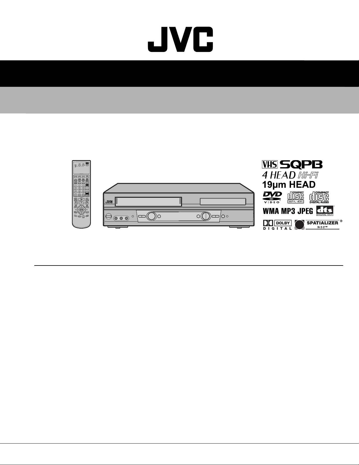
DVD/CD PLAYER Hi-Fi STEREO VIDEO CASSETTE RECORDER
HR-XVC20US,
SPECIFICATIONS
GENERAL
Power supply:
Power consumption:
Weight:
Dimensions:
Inputs/Outputs:
Video:
Audio:
Antenna:
Hi-Fi Frequency Response:
Hi-Fi Dynamic Range:
AC 120V 60Hz
Operation: 16W
Stand by: 2W
7.9lbs (3.6 kg)
Width : 16-15/16 inches (430 mm)
Height: 3-7/8 inches (99 mm)
Depth : 9-13/16 inches (249 mm)
In: 1Vp-p/75 ohm
Out: 1Vp-p/75 ohm
In:
Out:
UHF/VHF IN/OUT: 75 ohm coaxial
20Hz to 20,000Hz
More than 90dB
HR-XVC21U
(The specifications shown pertain specifically to the model HR-XVC20US.)
DVD section
Signal system:
Applicable disc:
Audio characteristics:
Frequency response:
S/N Ratio:
Harmonic distortion:
Wow and flutter:
Dynamic range:
Output:
-
8 dBm/50K ohm
-
8 dBm/1K ohm
Pickup:
C
NTSC
DVD (12cm, 8cm), CD (12cm, 8cm)
DVD: 4Hz - 22KHz
CD: 4Hz - 20KHz
90dB
0.02%
Below Measurable Level
90dB
Video : (RCA) 1 Vp-p/75ohm
Audio : (RCA)
Digital Audio : 0.5Vp-p 75 ohm
CD : Wavelength: 775 - 805 nm
Maximum output power: 0.5 mW
DVD : Wavelength: 640 - 660 nm
Maximum output power: 1.0 mW
-
8 dBm/1Kohm
VCR section
Video Head:
Audio Track:
Tuner:
RF Channel Output:
F.FWD/REW Time:
4 Rotary Heads
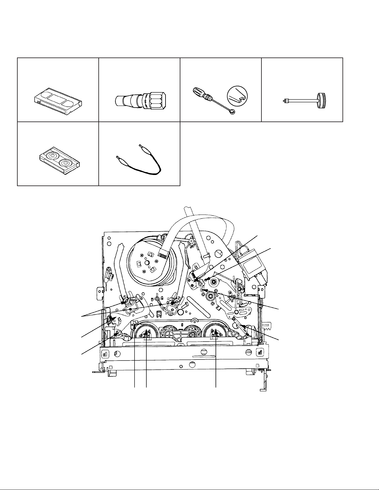
ACCESSORIES:
Hi-Fi Sound - 2 Tracks / MONO Sound - 1 Track
181 Channel Freq. Synthesized
VHF 2-13
UHF 14-69
CATV 14-36 (A)-(W)
37-59 (AA)-(WW)
60-85 (AAA)-(ZZZ)
86-94 (86)-(94)
95-99 (A-5)-(A-1)
100-125 (100)-(125)
01 (5A)
Channel 3 or 4, Switchable
Approx. 1 minute 48 seconds (with T-120 Cassette Tape) (at+25°C)
This service manual is printed on 100% recycled paper.
COPYRIGHT © 2002 VICTOR COMPANY OF JAPAN, LTD
Remote control x 1
Batteries (2 x AA)
75 ohm Coaxial Cable x 1
AUDIO/VIDEO Cable x 1
HR-XVC20US, HR-XVC21UC D2VP11
No.82948
2002/12
Page 2

TABLE OF CONTENTS
Section Title Page Section Title Page
Important Safety Precautions
INSTRUCTIONS
DISASSEMBLY INSTRUCTIONS
1.
REMOVAL OF MECHANICAL PARTS AND P.C.BOARDS ...............
1-1 TOP CABINET AND FRONT CABINET............................ 1-1
1-2 FLAP ..................................................................................1-1
1-3 DECK CD........................................................................... 1-1
1-4 VCR DECK ........................................................................1-2
1-5 VCR/DVD PCB ..................................................................1-2
2. REMOVAL OF VCR DECK PARTS.........................................1-3
2-1 TOP BRACKET..................................................................1-3
2-2 CASSETTE HOLDER ASS’Y.............................................1-3
2-3 CASSETTE SIDE L/R ........................................................1-3
2-4 LINK UNIT .........................................................................1-3
2-5 LINK LEVER / FLAP LEVER ............................................. 1-3
2-6 LOADING MOTOR / WORM..............................................1-4
2-7 TENSION ASS’Y................................................................1-4
2-8 T BRAKE ARM / T BRAKE BAND......................................1-5
S REEL / T REEL / IDLER ARM ASS’Y / IDLER GEAR ..............
2-9
2-10
CASSETTE OPENER / PINCH ROLLER BLOCK / P5 ARM ASS’Y.............
2-11 A/C HEAD ........................................................................ 1-6
2-12 FE HEAD .........................................................................1-6
2-13 CYLINDER UNIT ASS’Y ..................................................1-6
2-14 CAPSTAN DD UNIT.........................................................1-7
MAIN CAM / PINCH ROLLER CAM / JOINT GEAR ............
2-15
2-16 LOADING GEAR S/T UNIT..............................................1-7
2-17
CLUTCH ASS’Y / RING SPRING / CLUTCH LEVER / CLUTCH GEAR ...............
2-18
CASSETTE GUIDE POST / INCLINED BASE S/T UNIT / P4 CAP..............
REMOVAL AND INSTALLATION OF FLAT PACKAGE IC ...........
3.
REMOVAL................................................................................1-9
INSTALLATION ......................................................................1-10
KEY TO ABBREVIATIONS ...................................................... 1-11
SERVICE MODE LIST.............................................................. 1-13
WHEN “N” IS ALWAYS BEING DISPLAYED ON THE TV MONITOR .
PARENTAL CONTROL - RATING LEVEL 4-DIGIT PASSWORD CANNCELLATION .
WHEN REPLACING EEPROM(MEMORY) IC ......................... 1-14
PREVENTIVE CHECKS AND SERVICE INTERVALS............. 1-15
CONFIRMATION OF HOURS USED ....................................... 1-15
CLEANING ...............................................................................1-15
SERVICING FIXTURES AND TOOLS...................................... 1-16
MECHANISM ADJUSTMENT PARTS LOCATION GUIDE............
MECHANICAL ADJUSTMENT ................................................ 1-17
TAPE REMOVAL METHOD AT NO POWER SUPPLY ..........1-17
DISC REMOVAL METHOD AT NO POWER SUPPLY...........1-17
1. CONFIRMATION AND ADJUSTMENT .................................1-17
1-1
CONFIRMATION AND ADJUSTMENT OF TENSION POST POSITION .
1-2 CONFIRMATION OF PLAYBACK TORQUE AND
BACK TENSION TORQUE DURING PLAYBACK...........1-17
1-3 CONFIRMATION OF VSR TORQUE...............................1-17
1-4 CONFIRMATION OF REEL BRAKE TORQUE................1-18
2. CONFIRMATION AND ADJUSTMENT OF TAPE
RUNNING MECHANISM ..................................................1-18
2-1 GUIDE ROLLER .............................................................. 1-18
CONFIRMATION AND ADJUSTMENT OF AUDIO/CONTROL HEAD .
2-2
TAPE RUNNING ADJUSTMENT(X-VALUE ADJUSTMENT) .
2-3
ELECTRICAL ADJUSTMENTS ............................................... 1-20
1. BASIC ADJUSMENT ............................................................1-20
1-1 SWITCHING POINT ........................................................1-20
ELECTRICAL ADJUSTMENT PARTS LOCATION GUIDE ............
IC DESCRIPTIONS ..................................................................1-21
SERVO TIMING CHART .......................................................... 1-24
MECHANISM TIMING CHART................................................. 1-25
TROUBLE SHOOTING GUIDE ................................................ 1-26
(VCR SECTION) .................................................................... 1-26
(DVD SECTION) .................................................................... 1-49
CHARTS AND DIAGRAMS
1-1
INTERCONNECTION DIAGRAM ............................................2-1
Y/C/AUDIO/CCD/HEAD AMP SCHEMATIC DIAGRAM .......... 2-3
VCR SYSCON SCHEMTAIC DIAGRAM .................................2-5
TUNER/JACK SCHEMATIC DIAGRAM ..................................2-7
OPERATION/DISPLAY SCHEMATIC DIAGRAM.................... 2-9
HI-FI/DEMODULATOR SCHEMATIC DIAGRAM .................. 2-11
POWER SCHEMATIC DIAGRAM .........................................2-13
MPEG/MICOM SCHEMATIC DIAGRAM ............................... 2-15
MEMORY SCHEMATIC DIAGRAM .......................................2-17
DSP SCHEMATIC DIAGRAM................................................ 2-19
MOTOR DRV SCHEMATIC DIAGRAM ................................. 2-21
READ CHANNEL SCHEMATIC DIAGRAM ...........................2-23
AUDIO/VIDEO SCHEMATIC DIARAM ..................................2-25
OPERATION SCHEMATIC DIAGRAM ..................................2-27
PRINTED CIRCUIT BOARD OPERATION............................ 2-29
1-5
PRINTED CIRCUIT BOARD VCR/DVD................................. 2-31
1-6
WAVEFORMS .......................................................................2-35
DVD BLOCK DIAGRAM ........................................................2-37
Y/C/AUDIO/CCD/HEAD AMP BLOCK DIAGRAM ................. 2-39
SYSTEM CONTROL BLOCK DIAGRAM............................... 2-41
HI-FI/DEMODULATOR BLOCK DIAGRAM ........................... 2-43
1-7
TUNER/JACK BLOCK DIAGRAM .........................................2-45
POWER BLOCK DIAGRAM ..................................................2-47
1-8
1-8
PARTS LIST
1-9
3.1 PACKING AND ACCESSORY ASSEMBLY<M1> ................ 3-1
3.2 FINAL ASSEMBLY<M2>...................................................... 3-2
3.3 MECHANISM ASSEMBLY<M4> .......................................... 3-4
3.4 ELECTRICAL PARTS LIST .................................................. 3-7
VCR/DVD BOARD ASSEMBLY<03> ....................................... 3-7
1-13
OPERATION BOARD ASSEMBLY<28> .................................3-15
1-13
REFERENCE
SEMICONDUCTOR BASE CONNECTIONS.......................... 4-1
GENERAL SPECIFICATIONS[HR-XVC20US] ........................4-2
1-16
1-17
1-19
1-19
1-20
Page 3
Important Safety Precautions
cut close to connector
Prior to shipment from the factory, JVC products are strictly inspected to conform with the recognized product safety and electrical codes
of the countries in which they are to be sold. However, in order to maintain such compliance, it is equally important to implement the
following precautions when a set is being serviced.
v
Precautions during Servicing
1. Locations requiring special caution are denoted by labels and
inscriptions on the cabinet, chassis and certain parts of the
product. When performing service, be sure to read and comply with these and other cautionary notices appearing in the
operation and service manuals.
2. Parts identified by the symbol and shaded ( ) parts are
critical for safety.
Replace only with specified part numbers.
Note: Parts in this category also include those specified to com-
ply with X-ray emission standards for products using
cathode ray tubes and those specified for compliance
with various regulations regarding spurious radiation
emission.
3. Fuse replacement caution notice.
Caution for continued protection against fire hazard.
Replace only with same type and rated fuse(s) as specified.
4. Use specified internal wiring. Note especially:
1) Wires covered with PVC tubing
2) Double insulated wires
3) High voltage leads
5. Use specified insulating materials for hazardous live parts.
Note especially:
1) Insulation Tape 3) Spacers 5) Barrier
2) PVC tubing 4) Insulation sheets for transistors
6. When replacing AC primary side components (transformers,
power cords, noise blocking capacitors, etc.) wrap ends of
wires securely about the terminals before soldering.
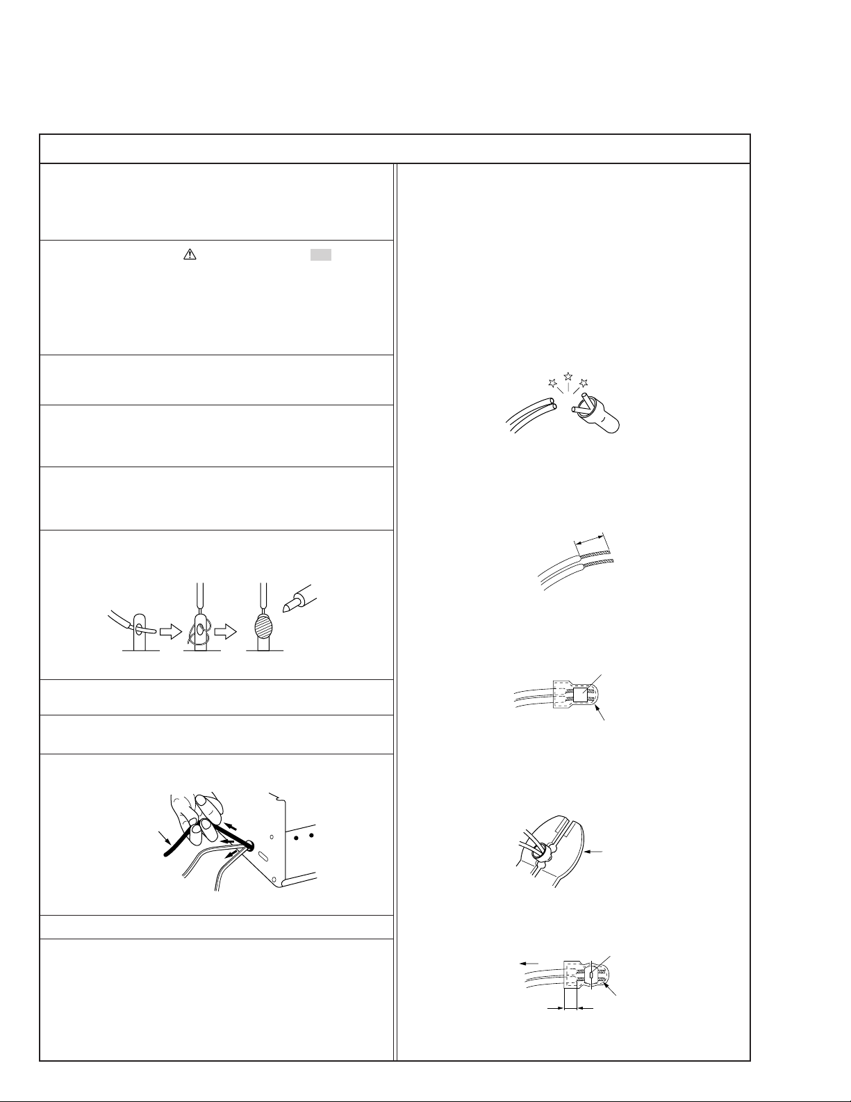
12. Crimp type wire connector
In such cases as when replacing the power transformer in sets
where the connections between the power cord and power
transformer primary lead wires are performed using crimp type
connectors, if replacing the connectors is unavoidable, in order to prevent safety hazards, perform carefully and precisely
according to the following steps.
1) Connector part number : E03830-001
2) Required tool : Connector crimping tool of the proper type
which will not damage insulated parts.
3) Replacement procedure
(1) Remove the old connector by cutting the wires at a point
close to the connector.
Important : Do not reuse a connector (discard it).
Fig.3
(2) Strip about 15 mm of the insulation from the ends of
the wires. If the wires are stranded, twist the strands to
avoid frayed conductors.
15 mm
Fig.1
7. Observe that wires do not contact heat producing parts
(heatsinks, oxide metal film resistors, fusible resistors, etc.)
8. Check that replaced wires do not contact sharp edged or
pointed parts.
9. When a power cord has been replaced, check that 10-15 kg of
force in any direction will not loosen it.
Power cord
Fig.2
10. Also check areas surrounding repaired locations.
11. Products using cathode ray tubes (CRTs)
In regard to such products, the cathode ray tubes themselves,
the high voltage circuits, and related circuits are specified for
compliance with recognized codes pertaining to X-ray emission.
Consequently, when servicing these products, replace the cathode ray tubes and other parts with only the specified parts.
Under no circumstances attempt to modify these circuits.
Unauthorized modification can increase the high voltage value
and cause X-ray emission from the cathode ray tube.
Fig.4
(3) Align the lengths of the wires to be connected. Insert
the wires fully into the connector.
Metal sleeve
Connector
Fig.5
(4) As shown in Fig.6, use the crimping tool to crimp the
metal sleeve at the center position. Be sure to crimp fully
to the complete closure of the tool.
1.25
2.0
5.5
Fig.6
(5) Check the four points noted in Fig.7.
Not easily pulled free
Wire insulation recessed
more than 4 mm
Fig.7
Crimping tool
Crimped at approx. center
of metal sleeve
Conductors extended
1
S40888-01
Page 4
v
d'
d
Chassis
Power cord,
primary wire
Region
USA & Canada
Europe & Australia
Grounding Impedance (Z)
Z 0.1 ohm
Z 0.5 ohm
≤
≤
AC inlet
Earth pin
Exposed accessible part
Milli ohm meter
Grounding Specifications
ab
c
V
Externally
exposed
accessible part
Z
Safety Check after Servicing
Examine the area surrounding the repaired location for damage or deterioration. Observe that screws, parts and wires have been
returned to original positions, Afterwards, perform the following tests and confirm the specified values in order to verify compliance with safety standards.
1. Insulation resistance test
Confirm the specified insulation resistance or greater between power cord plug prongs and
externally exposed parts of the set (RF terminals, antenna terminals, video and audio input
and output terminals, microphone jacks, earphone jacks, etc.). See table 1 below.
2. Dielectric strength test
Confirm specified dielectric strength or greater between power cord plug prongs and exposed
accessible parts of the set (RF terminals, antenna terminals, video and audio input and output
terminals, microphone jacks, earphone jacks, etc.). See table 1 below.
3. Clearance distance
When replacing primary circuit components, confirm specified clearance distance (d), (d’) between soldered terminals, and between terminals and surrounding metallic parts. See table 1
below.
Fig. 8
4. Leakage current test
Confirm specified or lower leakage current between earth ground/power cord plug prongs
and externally exposed accessible parts (RF terminals, antenna terminals, video and audio
input and output terminals, microphone jacks, earphone jacks, etc.).
Measuring Method : (Power ON)
Insert load Z between earth ground/power cord plug prongs and externally exposed accessible parts. Use an AC voltmeter to measure across both terminals of load Z. See figure 9 and
following table 2.
Fig. 9
5. Grounding (Class 1 model only)
Confirm specified or lower grounding impedance between earth pin in AC inlet and externally exposed accessible parts (Video in,
Video out, Audio in, Audio out or Fixing screw etc.).
Measuring Method:
Connect milli ohm meter between earth pin in AC inlet and exposed accessible parts. See figure 10 and grounding specifications.
Fig. 10
AC Line Voltage
100 V
100 to 240 V
110 to 130 V
110 to 130 V
200 to 240 V
Region
Japan
USA & Canada
Europe & Australia R 10 MΩ/500 V DC
Region Load Z
Insulation Resistance (R)
≤
R 1 MΩ/500 V DC
≥≥
1 MΩ R 12 MΩ/500 V DC
≤
Table 1 Specifications for each region
Dielectric Strength
AC 1 kV 1 minute
AC 1.5 kV 1 miute
AC 1 kV 1 minute
AC 3 kV 1 minute
AC 1.5 kV 1 minute
(Class 2)
(Class 1)
Clearance Distance (d), (d')
≤
d, d' 3 mm
≤
d, d' 4 mm
≤
d, d' 3.2 mm
≤
d 4 mm
≤
d' 8 mm (Power cord)
≤
d' 6 mm (Primary wire)
a, b, cLeakage Current (i)AC Line Voltage
100 V
110 to 130 V
110 to 130 V
220 to 240 V
Note: These tables are unofficial and for reference only. Be sure to confirm the precise values for your particular country and locality.
Japan
USA & Canada
Europe & Australia
Table 2 Leakage current specifications for each region
1 kΩ
0.15 µF
1.5 kΩ
2 kΩ
50 kΩ
2
≤
i 1 mA rms Exposed accessible parts
≤
i 0.5 mA rms
≤
i 0.7 mA peak
≤
i 2 mA dc
≤
i 0.7 mA peak
≤
i 2 mA dc
Exposed accessible parts
Antenna earth terminals
Other terminals
S40888-01
Page 5
DISASSEMBLY INSTRUCTIONS
1.
REMOVAL OF MECHANICAL PARTS AND P.C. BOARDS
1-1:
TOP CABINET AND FRONT CABINET
(Refer to Fig. 1-1)
1.
Remove the 5 screws 1.
2.
Remove the Top Cabinet in the direction of arrow (A).
3.
Disconnect the following connector: (CP651).
4.
Unlock the 8 supports 2.
5.
Remove the Front Cabinet in the direction of arrow (B).
6.
Remove the 2 screws 3.
7.
Remove the Operation PCB in the direction of arrow (C).
Top Cabinet
1
(A)
Front Cabinet
(B)
2
2
2
2
2
2
3
3
2
2
(C)
Operation PCB
CP651
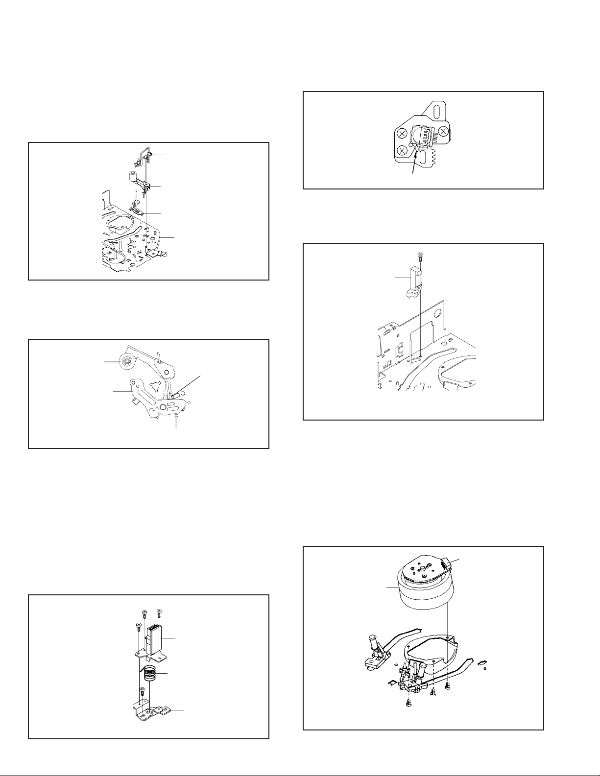
1-2: FLAP (Refer to Fig. 1-2)
1.2.Open Flap to 90˚ and flex in direction of arrow (A), at the
same time slide in direction of arrow (B).
Then lift in direction of arrow (C).
1
1
1
1
Fig. 1-1
1-3: DECK CD (Refer to Fig. 1-3)
1.
Make the short circuit on the position as shown Fig. 1-3
using a soldering. If you remove the Deck CD with no
soldering, the Laser may be damaged.
2.
Unlock the support 1 and remove the Deck Top Holder
in the direction of arrow (A).
3.
Remove the 2 screws 2.
4.
Remove the 2 screws 3.
5.
Disconnect the following connectors: (CP2301, CP2302,
CP2601).
6.
Remove the Deck CD in the direction of arrow (B).
7.
Remove the 3 screws 4.
8.
Remove the Front Angle in the direction of arrow (C).
Pick Up PCB
Make the sort circuit
using a soldering.
Fig. 1-3
Deck Top Holder
4
4
4
Deck CD
1
(A)
(C)
Front Angle
3
3
2
2
(B)
CP2601
CP2301
CP2302
NOTE
When the installation of the Deck CD, remove all the soldering on the short circuit position after the connection of Pick
Up PCB and VCR/DVD PCB connector.
(C)
(A)
(B)
Flap
Fig. 1-2
1-1
Page 6
DISASSEMBLY INSTRUCTIONS
1-4: VCR DECK (Refer to Fig. 1-4)
1.
Remove the 3 screws 2.
2.
Disconnect the following connectors: (CP101, CP102,
CP103 and CP3001).
3.
Remove the AC Head Cover and VCR Deck in the
direction of arrow.
1
1
VCR Deck
1
AC Head Cover
CP103
CP101
CP102
CP3001
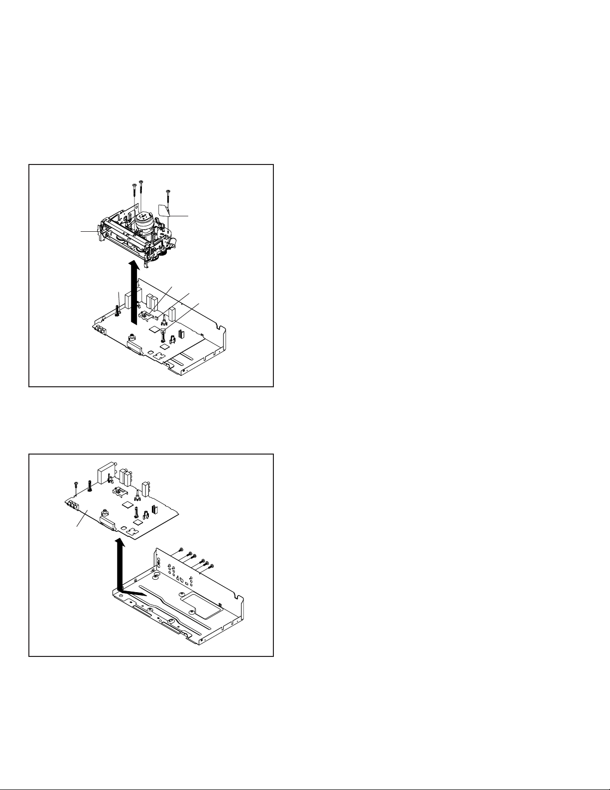
1-5: VCR/DVD PCB (Refer to Fig. 1-5)
1.
Remove the screw 1.
2.
Remove the 6 screws 2.
3.
Remove the VCR/DVD PCB in the direction of arrow.
2
VCR/DVD PCB
1
2
2
2
2
2
Fig. 1-4
1-2
Fig. 1-5
Page 7
DISASSEMBLY INSTRUCTIONS
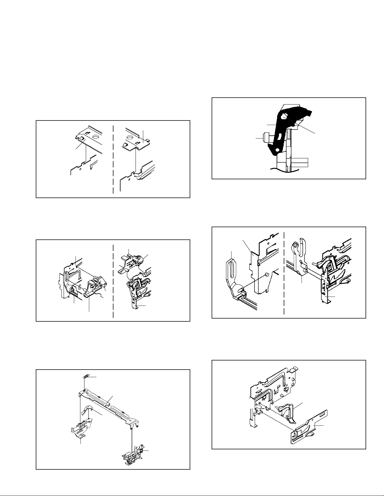
2. REMOVAL OF VCR DECK PARTS
2-1: TOP BRACKET (Refer to Fig. 2-1)
Extend the 2 supports 1.
1.
Slide the 2 supports 2 and remove the Top Bracket.
2.
NOTE
After the installation of the Top Bracket, bend the support
1.
1 so that the Top Bracket is fixed.
Top Bracket
1
Top Bracket
2
Main Chassis
2
Main Chassis
2-2: CASSETTE HOLDER ASS'Y (Refer to Fig. 2-2)
1.
Move the Cassette Holder Ass'y to the front side.
2.
Push the Locker R to remove the Cassette Side R.
3.
Remove the Cassette Side L.
Cassette Side R
Main Chassis
1
Locker R
Fig. 2-1
NOTE
In case of the Locker R installation, check if the one
1.
position of Fig. 2-3-B are correctly locked.
When you install the Cassette Side R, be sure to move
2.
the Locker R after installing.
Locker R
Check if this position
Cassette Side R
is locked.
2-4: LINK UNIT (Refer to Fig. 2-4)
1.
Set the Link Unit to the Eject position.
2.
Unlock the support 1.
3.
Remove the (A) side of the Link Unit first, then remove
the (B) side.
Main Chassis
Link Unit
Fig. 2-3-B
Link Unit
Cassette Side L
Main Chassis
2-3: CASSETTE SIDE L/R (Refer to Fig. 2-3-A)
1.
Remove the Locker Spring.
2.
Unlock the 4 supports 1 and then remove the Cassette
Side L/R.
3.
Unlock the support 2 and then remove the Locker R.
Locker Spring
1
1
2
Cassette Side R
Cassette Holder
Locker R
1
1
Cassette Side L
Fig. 2-2
(A)
(B)
Link Unit
Main Chassis
2-5: LINK LEVER/FLAP LEVER (Refer to Fig. 2-5)
1.
Extend the support 1.
2.
Remove the Link Lever.
3.
Remove the Flap Lever.
1
Flap Lever
Link Lever
Fig. 2-4
Fig. 2-5
Fig. 2-3-A
1-3
Page 8
DISASSEMBLY INSTRUCTIONS
2-6: LOADING MOTOR/WORM (Refer to Fig. 2-6-A)
1.
Remove the screw 1.
2.
Remove the Loading Motor.
3.
Remove the Worm.
Loading Motor
Worm
Main Chassis
• Screw Torque: 3 ± 0.5kgf•cm
1
Fig. 2-6-A
NOTE
1.
In case of the Worm installation, check if the value of the
Fig. 2-6-B is correct.
2.
In case of the Loading Motor installation, hook the wire on
the Cassette Opener as shown Fig. 2-6-C.
3.
When installing the wires between Capstan DD Unit and
Loading Motor, connect them correctly as shown Fig. 2-6-D.
19.2 ± 0.1mm
2-7: TENSION ASS’Y (Refer to Fig. 2-7-B)
Turn the Pinch Roller Cam clockwise so that the Tension
1.
Holder hook is set to the position of Fig. 2-7-A to move
the T ension Arm Ass’y .
2.
Remove the Tension Spring.
3.
Unlock the 2 supports 1 and remove the Tension Band.
4.
Unlock the support 2 and remove the Tension Arm Ass’y.
5.
Unlock the support 3 and remove the Tension Connect.
6.
Float the hook 4 and turn it clockwise then remove the
Tension Holder.
T ension Arm Ass’y
Fig. 2-7-A
1
Tension Connect
Tension Spring
2
4
1
3
Tension Holder
Tension Band
T ension Arm Ass’y
1-4
Loading Motor
-
+
Safety surface for pressing
of the insert.
Pink
White
Fig. 2-6-B
Loading Motor
Cassette Opener
Fig. 2-6-C
Capstan DD Unit
L2
L1
Fig. 2-6-D
Fig. 2-7-B
NOTE
1.
In case of the Tension Band installation, note the direction of the installation. (Refer to Fig. 2-7-C)
2.
In case of the Tension Band installation, install correctly
as Fig. 2-7-D.
3.
In case of the Tension Connect installation, install as the
circled section of Fig. 2-7-E.
Tension Connect
Tension Band
Fig. 2-7-C
Page 9
[OK]
[NG]
Tension Connect
Tension Connect
Tension Connect
DISASSEMBLY INSTRUCTIONS
NOTE
1.
Take care not to damage the gears of the S Reel and T
Tension Band
Tension Band
Fig. 2-7-D
Reel.
2.
The Polyslider Washer may be remained on the back of
the reel.
3.
Take care not to damage the shaft.
4.
Do not touch the section “A” of S Reel and T Reel. (Use
gloves.) (Refer to Fig. 2-9-A) Do not adhere the stains
on it.
5.
When you install the reel, clean the shaft and grease it
(FG-84M). (If you do not grease, noise may be heard in
FF/REW mode.)
6.
After installing the reel, adjust the height of the reel.
(Refer to MECHANICAL ADJUSTMENT)
Main Chassis
Fig. 2-7-E
2-8: T BRAKE ARM/T BRAKE BAND (Refer to Fig. 2-8-A)
Remove the T Brake Spring.
1.
Turn the T Brake Arm clockwise and bend the hook
2.
section to remove it.
Unlock the 2 supports 1 and remove the T Brake Band.
3.
T Brake Band
Hook section
1
1
T Brake Arm
T Brake Spring
Fig. 2-8-A
NOTE
1. In case of the T Brake Band installation, install correctly
as Fig. 2-8-B.
Idler Gear
Idler Arm Ass’y
S Reel
(A)
(B)
T Reel
1
(A)
1
Fig. 2-9-A
NOTE
1.2.In case of the S Reel and T Reel installation, check if the
correct parts are installed. (Refer to Fig. 2-9-B)
In case of the Idler Arm Ass’y installation, install correctly
as Fig. 2-9-C. And also set it so that the section “B” of
Fig. 2-9-A is placed under the Main Chassis tab.
[OK]
T Brake Band
[NG]
T Brake Band
T Brake Arm
T Brake Arm
Fig. 2-8-B
2-9: S REEL/T REEL/IDLER ARM ASS’Y/IDLER GEAR
(Refer to Fig. 2-9-A)
1.
Remove the S Reel and T Reel.
2.
Remove the 2 Polyslider Washers 1.
3.
Remove the Idler Arm Ass’y and Idler Gear.
[OK]
[NG]
Clutch Gear
Clutch Gear
Big Hole
(S Reel)
Small Hole
(T Reel)
Fig. 2-9-B
Idler Arm Ass’y
Idler Arm Ass’y
Fig. 2-9-C
1-5
Page 10
DISASSEMBLY INSTRUCTIONS
2-10: CASSETTE OPENER/PINCH ROLLER BLOCK/P5
ARM ASS’Y (Refer to Fig. 2-10-A)
1.2.Unlock the support 1 and remove the Cassette Opener.
Remove the Pinch Roller Block and P5 Ar m Ass’y.
1
Cassette Opener
Pinch Roller Block
P5 Arm Ass’y
Main Chassis
Fig. 2-10-A
NOTE
1.2.Do not touch the Pinch Roller. (Use gloves.)
In case of the Pinch Roller Block and the Pinch Roller
Cam installation, install correctly as Fig. 2-10-B.
Pinch Roller Block
P5 Arm Ass’y
Can be seen the hole of the
Main Cam.
Can be seen the hole of
the Pinch Roller Cam.
Fig. 2-10-B
2-11: A/C HEAD (Refer to Fig. 2-11-A)
1.
Remove the screw 1.
2.
Remove the A/C Head Base.
3.
Remove the 3 screws 2.
4.
Remove the A/C Head and A/C Head Spring.
NOTE
1.
Do not touch the A/C Head. (Use gloves.)
2.
When you install the A/C Head Spring, install as shown in
Fig. 2-11-B.
3.
When you install the A/C Head, tighten the screw (1) first,
then tighten the screw (2), finally tighten the screw (3).
(3)
(1)
2
2
(2)
2
A/C Head
Spring Position
Fig. 2-11-B
2-12: FE HEAD (RECORDER ONLY) (Refer to Fig. 2-12)
1.2.Remove the screw 1.
Remove the FE Head.
1
FE Head
• Screw Torque: 5 ± 0.5kgf•cm
• The FE Head is not installed on the Video Cassette Player.
Fig. 2-12
2-13: CYLINDER UNIT ASS’Y (Refer to Fig. 2-13)
1.
Disconnect the following connector:
(CD2001)
2.
Remove the 3 screws 1.
3.
Remove the Cylinder Unit Ass’y.
NOTE
1. When you install the Cylinder Unit Ass’y, tighten the
screws from (1) to (3) in order while pulling the Ass’y
toward the left front direction.
CD2001
Cylinder Unit Ass’y
• Screw Torque: 5 ± 0.5kgf•cm (Screw 1)
1-6
A/C Head Spring
1
A/C Head Base
• Screw Torque: 3 ± 0.5kgf•cm
(2)
(1)
1
(3)
1
1
Fig. 2-13
Fig. 2-11-A
Page 11
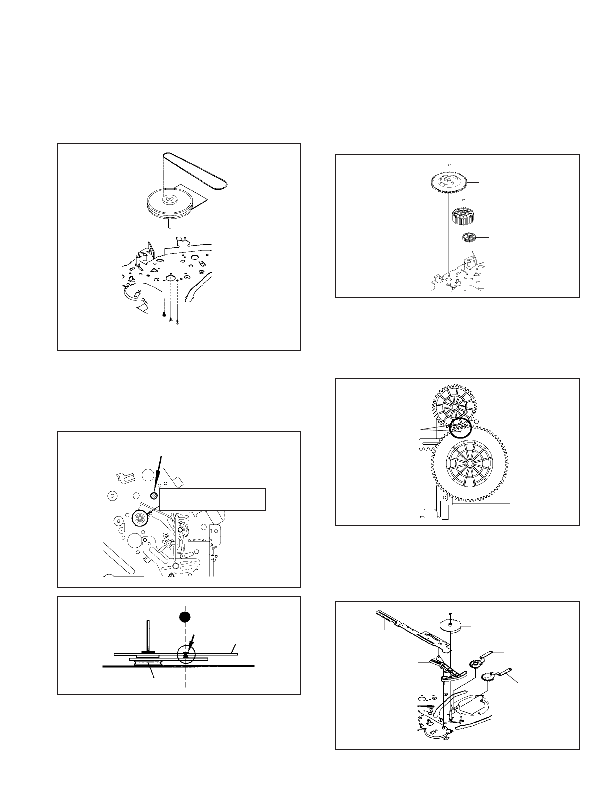
DISASSEMBLY INSTRUCTIONS
2-14: CAPSTAN DD UNIT (Refer to Fig. 2-14-A)
1.
Remove the Capstan Belt.
2.
Remove the 3 screws 1.
3.
Remove the Capstan DD Unit.
Capstan Belt
Capstan DD Unit
1
1
1
• Screw Torque: 4 ± 0.5kgf•cm
Fig. 2-14-A
NOTE
1. In case of the Capstan DD Unit installation, apply the
silicon bond (TSE3843-W) on the position Fig. 2-14-B
correctly. (If no silicon bond applied, abnormal noise will
be heard on the deck operation.)
(Refer to Fig. 2-14-B, C)
Applied position of
silicon bond
2-15: MAIN CAM/PINCH ROLLER CAM/JOINT GEAR
(Refer to Fig. 2-15-A)
1.2.Remove the E-Ring 1, then remove the Main Cam.
Remove the E-Ring 2, then remove the Pinch Roller
Cam and Joint Gear.
1
Main Cam
2
Pinch Roller Cam
Joint Gear
Fig. 2-15-A
NOTE
1. In case of the Pinch Roller Cam and Main Cam installation, install them as the circled section of Fig. 2-15-B so
that the each markers are met. (Refer to Fig. 2-15-B)
And also can be seen the Main Chassis hole through the
Main Cam maker hole.
Pinch Roller Cam
Marker
Main Cam
Be careful not to apply the silicon
bond to the Pinch Roller.
Capstan DD Unit
Silicon Bond
Main Chassis
Fig. 2-14-B
Fig. 2-14-C
Fig. 2-15-B
2-16: LOADING GEAR S/T UNIT (Refer to Fig. 2-16-A)
1.2.Remove the E-Ring 1 and remove the Main Loading
Gear.
Remove the Main Rod, Tension Lever, Loading Arm S
Unit and Loading Arm T Unit.
1
Main Rod
Tension Lever
Main Loading Gear
Loading Arm T Unit
Loading Arm S Unit
Fig. 2-16-A
1-7
Page 12
DISASSEMBLY INSTRUCTIONS
NOTE
1. When you install the Loading Arm S Unit, Loading Arm T
Unit and Main Loading Gear, align each marker. (Refer
to Fig. 2-16-B)
Marker
Main Loading Gear
Marker
Loading Arm T Unit Loading Arm S Unit
Fig. 2-16-B
2-17: CLUTCH ASS’Y/RING SPRING/CLUTCH LEVER/
CLUTCH GEAR (Refer to Fig. 2-17-A)
1.
Remove the Polyslider Washer 1.
2.
Remove the Clutch Ass’y and Ring Spring.
3.
Remove the Clutch Lever.
4.
Remove the Coupling Gear, Coupling Spring and Clutch
Gear.
1
Clutch Ass’y
Ring Spring
Coupling Gear
Coupling Spring
Clutch Gear
Clutch Lever
2-18: CASSETTE GUIDE POST/INCLINED BASE S/T
UNIT/P4 CAP (Refer to Fig. 2-18-A)
1.
Remove the P4 Cap.
2.
Unlock the support 1 and remove the Cassette Guide
Post.
3.
Remove the Inclined Base S/T Unit.
4.
Remove the screw 2.
5.
Remove the LED Reflector.
Cassette Guide Post
Inclined Base T
Unit
P4 Cap
2
Fig. 2-18-A
Inclined Base S
Unit
LED Reflector
1
NOTE
1.
Do not touch the roller of Guide Roller.
2.
In case of the P4 Cap installation, install it with parallel
for “A” and “B” of Fig. 2-18-B.
3.
In case of the Cassette Guide Post installation, install
correctly as the circled section of Fig. 2-18-C.
“A” “B”
Fig. 2-17-A
NOTE
1. In case of the Clutch Ass’y installation, install it with
inserting the spring of the Clutch Ass’y into the dent of the
Coupling Gear. (Refer to Fig. 2-17-B)
Clutch Ass’y
Coupling Gear
Fig. 2-17-B
1-8
P4 Cap
[OK]
Cassette Guide Post
[NG]
Cassette Guide Post
Cassette Opener
Fig. 2-18-B
Fig. 2-18-C
Page 13
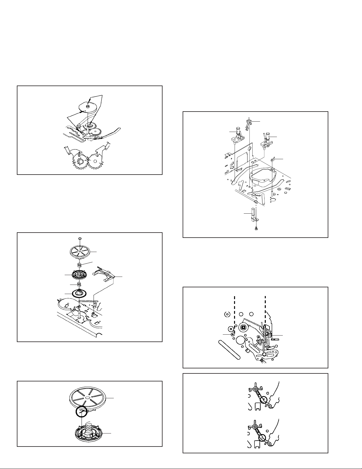
DISASSEMBLY INSTRUCTIONS
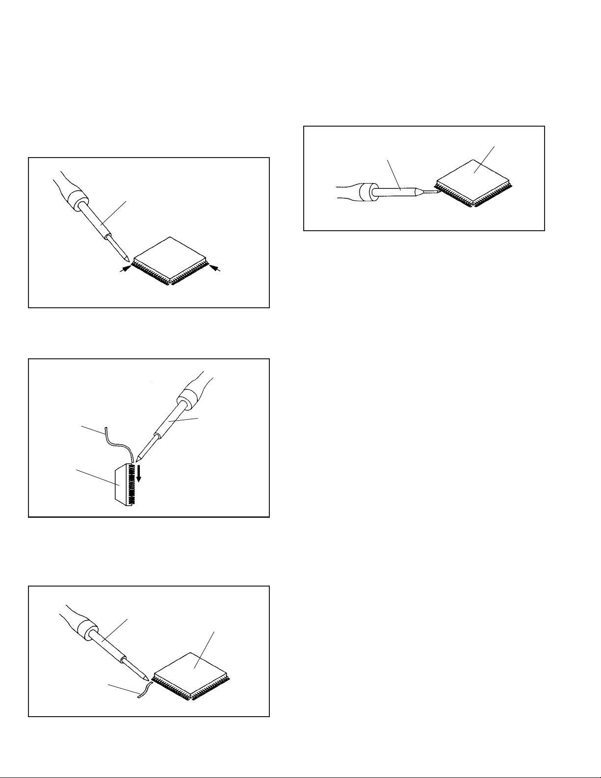
3. REMOVAL AND INSTALLATION OF FLAT PACKAGE IC
REMOVAL
1. Put the Masking Tape (cotton tape) around the Flat
Package IC to protect other parts from any damage.
(Refer to Fig. 3-1.)
NOTE
Masking is carried out on all the parts located within
10 mm distance from IC leads.
Masking Tape
(Cotton Tape)
2. Heat the IC leads using a blower type IC desoldering
machine. (Refer to Fig. 3-2.)
NOTE
Do not add the rotating and the back and forth directions force on the IC, until IC can move back and forth
easily after desoldering the IC leads completely.
IC
Fig. 3-1
Blower type IC
desoldering machine
3. When IC starts moving back and forth easily after
desoldering completely, pickup the corner of the IC using
a tweezers and remove the IC by moving with the IC
desoldering machine. (Refer to Fig. 3-3.)
NOTE
Some ICs on the PCB are affixed with glue, so be
careful not to break or damage the foil of each IC
leads or solder lands under the IC when removing it.
Blower type IC
desoldering machine
Tweezers
IC
4.5.Peel off the Masking Tape.
Absorb the solder left on the pattern using the Braided
Shield Wire. (Refer to Fig. 3-4.)
NOTE
Do not move the Braided Shield Wire in the vertical
direction towards the IC pattern.
Fig. 3-3
Braided Shield Wire
Soldering Iron
IC
Fig. 3-2
IC pattern
Fig. 3-4
1-9
Page 14
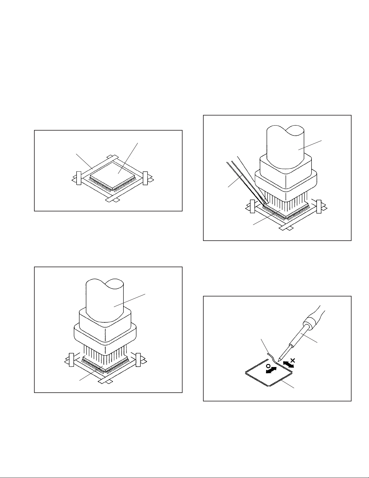
DISASSEMBLY INSTRUCTIONS
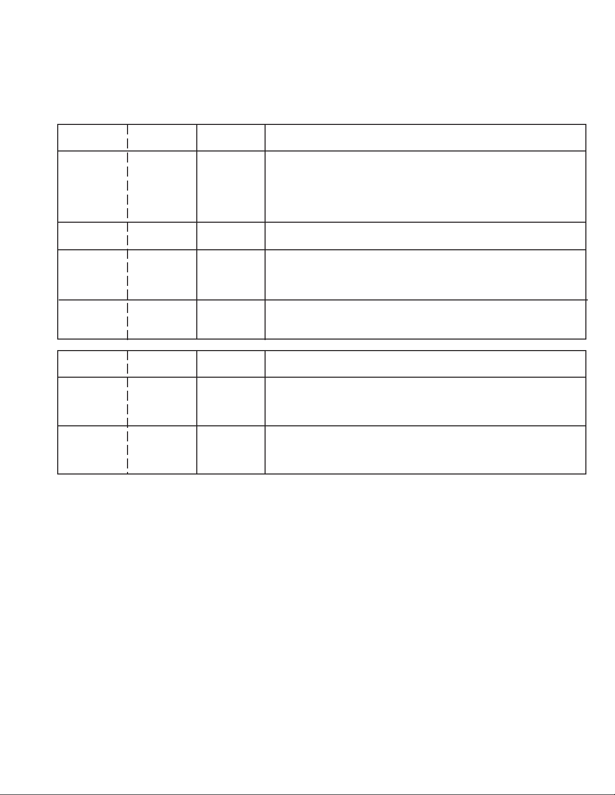
INSTALLATION
1. Take care of the polarity of new IC and then install the
new IC fitting on the printed circuit pattern. Then solder
each lead on the diagonal positions of IC temporarily.
(Refer to Fig. 3-5.)
Soldering Iron
Solder temporarily
Solder temporarily
Fig. 3-5
2. Supply the solder from the upper position of IC leads
sliding to the lower position of the IC leads.
(Refer to Fig. 3-6.)
4. When bridge-soldering between terminals and/or the
soldering amount are not enough, resolder using a Thintip Soldering Iron. (Refer to Fig. 3-8.)
IC
Thin-tip Soldering Iron
Fig. 3-8
5. Finally, confirm the soldering status on four sides of the
IC using a magnifying glass.
Confirm that no abnormality is found on the soldering
position and installation position of the parts around the
IC. If some abnormality is found, correct by resoldering.
NOTE
When the IC leads are bent during soldering and/or
repairing, do not repair the bending of leads. If the
bending of leads are repaired, the pattern may be
damaged. So, be always sure to replace the IC in this
case.
Solder
IC
Supply soldering
from upper position
to lower position
Soldering Iron
Fig. 3-6
3. Absorb the solder left on the lead using the Braided
Shield Wire. (Refer to Fig. 3-7.)
NOTE
Do not absorb the solder to excess.
Soldering Iron
IC
Braided Shield Wire
1-10
Fig. 3-7
Page 15

A
A/C
ACC
AE
AFC
AFT
AFT DET
AGC
AMP
ANT
A.PB
APC
ASS’Y
AT
AUTO
A/V
B
BGP
BOT
BPF
BRAKE SOL
BUFF
B/W
C
C
CASE
CAP
CARR
CH
CLK
CLOCK (SY-SE)
COMB
CONV
CPM
CTL
CYL
CYL-M
CYL SENS
D
DATA (SY-CE)
dB
DC
DD Unit
DEMOD
DET
DEV
E
E
EF
EMPH
ENC
ENV
EOT
EQ
EXT
F
F
FBC
FE
FF
FG
FL SW
FM
FSC
FWD
G
GEN
GND
H
H.P.F
KEY TO ABBREVIATIONS
:
Audio/Control
:
Automatic Color Control
:
Audio Erase
:
Automatic Frequency Control
:
Automatic Fine Tuning
:
Automatic Fine Tuning Detect
:
Automatic Gain Control
:
Amplifier
:
Antenna
:
Audio Playback
:
Automatic Phase Control
:
Assembly
:
All Time
:
Automatic
:
Audio/Video
:
Burst Gate Pulse
:
Beginning of Tape
:
Bandpass Filter
:
Brake Solenoid
:
Buffer
:
Black and White
:
Capacitance, Collector
:
Cassette
:
Capstan
:
Carrier
:
Channel
:
Clock
:
Clock (Syscon to Servo)
:
Combination, Comb Filter
:
Converter
:
Capstan Motor
:
Control
:
Cylinder
:
Cylinder-Motor
:
Cylinder-Sensor
:
Data (Syscon to Servo)
:
Decibel
:
Direct Current
:
Direct Drive Motor Unit
:
Demodulator
:
Detector
:
Deviation
:
Emitter
:
Emitter Follower
:
Emphasis
:
Encoder
:
Envelope
:
End of Tape
:
Equalizer
:
External
:
Fuse
:
Feed Back Clamp
:
Full Erase
:
Fast Forward, Flipflop
:
Frequency Generator
:
Front Loading Switch
:
Frequency Modulation
:
Frequency Sub Carrier
:
Forward
:
Generator
:
Ground
:
High Pass Filter
H.SW
Hz
IC
I
IF
IND
INV
KIL
K
L
L
LED
LIMIT AMP
LM, LDM
LP
L.P.F
LUMI.
M
M
MAX
MINI
MIX
MM
MOD
MPX
MS SW
NC
N
NR
OSC
O
OPE
PB
P
PB CTL
PB-C
PB-Y
PCB
P. CON
PD
PG
P-P
R
R
REC
REC-C
REC-Y
REEL BRK
REEL S
REF
REG
REW
REV, RVS
RF
RMC
RY
S. CLK
S
S. COM
S. DATA
SEG
SEL
SENS
SER
SI
SIF
SO
SOL
SP
STB
SW
:
Head Switch
:
Hertz
:
Integrated Circuit
:
Intermediate Frequency
:
Indicator
:
Inverter
:
Killer
:
Left
:
Light Emitting Diode
:
Limiter Amplifier
:
Loading Motor
:
Long Play
:
Low Pass Filter
:
Luminance
:
Motor
:
Maximum
:
Minimum
:
Mixer, mixing
:
Monostable Multivibrator
:
Modulator, Modulation
:
Multiplexer, Multiplex
:
Mecha State Switch
:
Non Connection
:
Noise Reduction
:
Oscillator
:
Operation
:
Playback
:
Playback Control
:
Playback-Chrominance
:
Playback-Luminance
:
Printed Circuit Board
:
Power Control
:
Phase Detector
:
Pulse Generator
:
Peak-to Peak
:
Right
:
Recording
:
Recording-Chrominance
:
Recording-Luminance
:
Reel Brake
:
Reel Sensor
:
Reference
:
Regulated, Regulator
:
Rewind
:
Reverse
:
Radio Frequency
:
Remote Control
:
Relay
:
Serial Clock
:
Sensor Common
:
Serial Data
:
Segment
:
Select, Selector
:
Sensor
:
Search Mode
:
Serial Input
:
Sound Intermediate Frequency
:
Serial Output
:
Solenoid
:
Standard Play
:
Serial Strobe
:
Switch
1-11
Page 16

S
SYNC
SYNC SEP
T
TR
TRAC
TRICK PB
TP
U
UNREG
V
V
VCO
VIF
VP
V. P B
VR
V.REC
VSF
VSR
VSS
V-SYNC
VT
X
X’TAL
Y
Y/C
KEY TO ABBREVIATIONS
:
Synchronization
:
Sync Separator, Separation
:
Transistor
:
Tracking
:
Trick Playback
:
Test Point
:
Unregulated
:
Volt
:
Voltage Controlled Oscillator
:
Video Intermediate Frequency
:
Vertical Pulse, Voltage Display
:
Video Playback
:
Variable Resistor
:
Video Recording
:
Visual Search Fast Forward
:
Visual Search Rewind
:
Voltage Super Source
:
Vertical-Synchronization
:
Voltage Tuning
:
Crystal
:
Luminance/Chrominance
1-12
Page 17
SERVICE MODE LIST
This unit provided with the following SERVICE MODES so you can repair, examine and adjust easily.
To enter to the SERVICE MODE function, press and hold both buttons simultaneously on the main unit or on the main unit and on
the remote control for more than a standard time (second).
Set Key
CH UP
CH UP STOP 2
CH UP PLAY 2
CH DOWN POWER 2
Set Key OperationsRemocon Key
REC 4 2
STOP 7 3
Set Key
FF 2
Standard Time
(seconds)
Standard Time
(seconds)
Operations
PLAY/REC total hours are displayed on the TV Monitor.
Refer to the “PREVENTIVE CHECKS AND SERVICE INTERVALS”
(CONFIRMATION OF HOURS USED).
Can be checked of the INITIAL DATA of MEMORY IC.
Refer to the “WHEN REPLACING EEPROM (MEMORY) IC”.
Adjust the SWITHCHING POINT automatically.
Refer to the “ELECTRICAL ADJUSTMENT” (SWITHCHING POINT).
Initialization of the factory on VCR.
NOTE: Do not use this for the normal servicing.
If you set a factory initialization, the memories are reset such as
the clock setting, the channel setting, and PLAY/REC total hours.
VCR operation mode at no connection of DVD.
Refer to the “PREPARATION FOR SERVICING”
NOTE: Although the DVD is connected, the DVD mode cannot be selected.
Initialization of the factory on DVD.
NOTE:
Releasing of PARENTAL LOCK.
Refer to the “PARENTAL CONTROL - RATING LEVEL”.
NOTE:
The function will only work without the setting of DVD disc at DVD
mode.
Do not use this for the normal servicing.
The function will only work without the setting of DVD disc at DVD
mode.
<NOTE> WHEN "N" IS ALWAYS BEING DISPLAYED ON THE TV MONITOR.
(REMOTE CONTROLLER FORMAT)
This product is usable the remote controller which is used by DVD+VHS of the other brand.
If "N" is always being displayed on the TV monitor, can not control from provided remote controller since this product is other
brand format.
• How to return a JVC format.
Turn off the power of the set and push the CHANNEL+ button and the REC button of the set simultaneously.
PARENTAL CONTROL - RATING LEVEL (4 DIGIT PASSWORD CANCELLATION)
If the stored 4 digit password in the Rating Level menu needs to be cancelled, please follow the steps below.
Turn Unit ON.
1.
Press and hold the '7' key on the remote control unit.
2.
Simultaneously press and hold the 'STOP' key on the front panel.
3.
Hold both keys for more than 3 seconds.
4.
The On Screen Display message 'PASSWORD CLEAR' will appear.
5.
The 4 digit password has now been cleared.
6.
1-13
Page 18
WHEN REPLACING EEPROM (MEMORY) IC
If a service repair is undertaken where it has been required to change the MEMORY IC, the following steps should be taken to
ensure correct data settings while making reference to TABLE 1.
NOTE: No need setting for after INI 2F.
INI +0 +1 +2 +3 +4 +5 +6 +7 +8 +9 +A +B +C +D +E +F
ADDRESS DATA
00 0E 30 BA 60 64 64 4A 86 0B 2B 86 32 8A 08 0A 0F
10 AF 97 95 8A A0 55 31 04 88 A5 9F 3A
10 BF 00
00
PLAY/REC
20 3A 11 22 70 61 2A 3A 00 00 00 00 85 A2 B0 00 00
1.
Connect the set to TV Monitor.
2.
Turn on the POWER.
3.
Press both CH UP button on the set and the FF button on the set for more than 2 seconds.
Table 1
ADDRESS and DATA will appear on TV Monitor as Fig 1.
4.
ADDRESS is now selected and should “blink”. Using the SET + or - button on the remote,
step through the ADDRESS until required ADDRESS to be changed is reached.
5.
Press ENTER to select DATA. When DATA is selected, it will “blink”.
6.
Again, step through the DATA using SET + or - button until required DATA value has been selected.
7.
Pressing ENTER will take you back to ADDRESS for further selection if necessary.
8.
Repeat steps 4 to 7 until all data has been checked.
9.
When satisfied correct DATA has been entered, turn POWER off (return to STANDBY MODE) to finish DATA input.
After the data input, set to the initializing of shipping.
10.
Turn on the POWER.
11.
Press both CH UP button on the set and the PLAY button on the set for more than 2 seconds.
12.
After the finishing of the initializing of shipping, the unit will turn off automatically.
The unit will now have the correct DATA for the new MEMORY IC.
INIT 00 0E
0003
Fig. 1
1-14
Page 19
PREVENTIVE CHECKS AND SERVICE INTER VALS
The following standard table depends on environmental conditions and usage.
Parts replacing time does not mean the life span for individual parts.
Also, long term storage or misuse may cause transformation and aging of rubber parts.
The following list means standard hours, so the checking hours depends on the conditions.
Time
Parts Name
Audio Control Head
Full Erase Head
(Recorder only)
Capstan Belt
Pinch Roller
Capstan DD Unit
Loading Motor
Tension Band
T Brake Band
Clutch Ass’y
Idler Arm Ass’y
Capstan Shaft
Tape Running
Guide Post
Cylinder Unit
500
hours
1,000
hours
1,500
hours
2,000
hours
2,500
hours
CONFIRMATION OF HOURS USED
PLAY/REC total hours can be checked on the FIP.
Total hours are displayed in 16 system of notation.
NOTE: If you set a factory initialization, the total hours is reset to “0”.
1.
Connect the set to TV Monitor.
2.
Turn on the POWER.
3.
Press both CH UP button on the set and the FF button on
the set for more than 2 seconds.
4.
After the confirmation of using hours, turn off the power.
INIT 00 0E
PLAY/REC 0003
Notes
Clean those parts in
contact with the tape.
Clean the rubber, and parts
which the rubber touches.
Replace when rolling
becomes abnormal.
Clean the Head
Initial setting content of MEMORY IC.
PLAY/REC total hours.
= (16 x 16 x 16 x thousands digit value)
+ (16 x 16 x hundreds digit value)
+ (16 x tens digit value)
+ (ones digit value)
: Clean
: Check it and if
necessary, replace it.
CLEANING
NOTE
After cleaning the heads with isopropyl alcohol, do not
run a tape until the heads dry completely. If the heads are
not completely dry and alcohol gets on the tape, damage
may occur.
1. AUDIO CONTROL HEAD
Clean the Audio Control Head with the cotton stick
soaked by alcohol. Clean the full erase head in the same
manner. (Refer to the figure below.)
Audio Control Head
2. TAPE RUNNING SYSTEM
When cleaning the tape transport system, use the gauze
moistened with isopropyl alcohol.
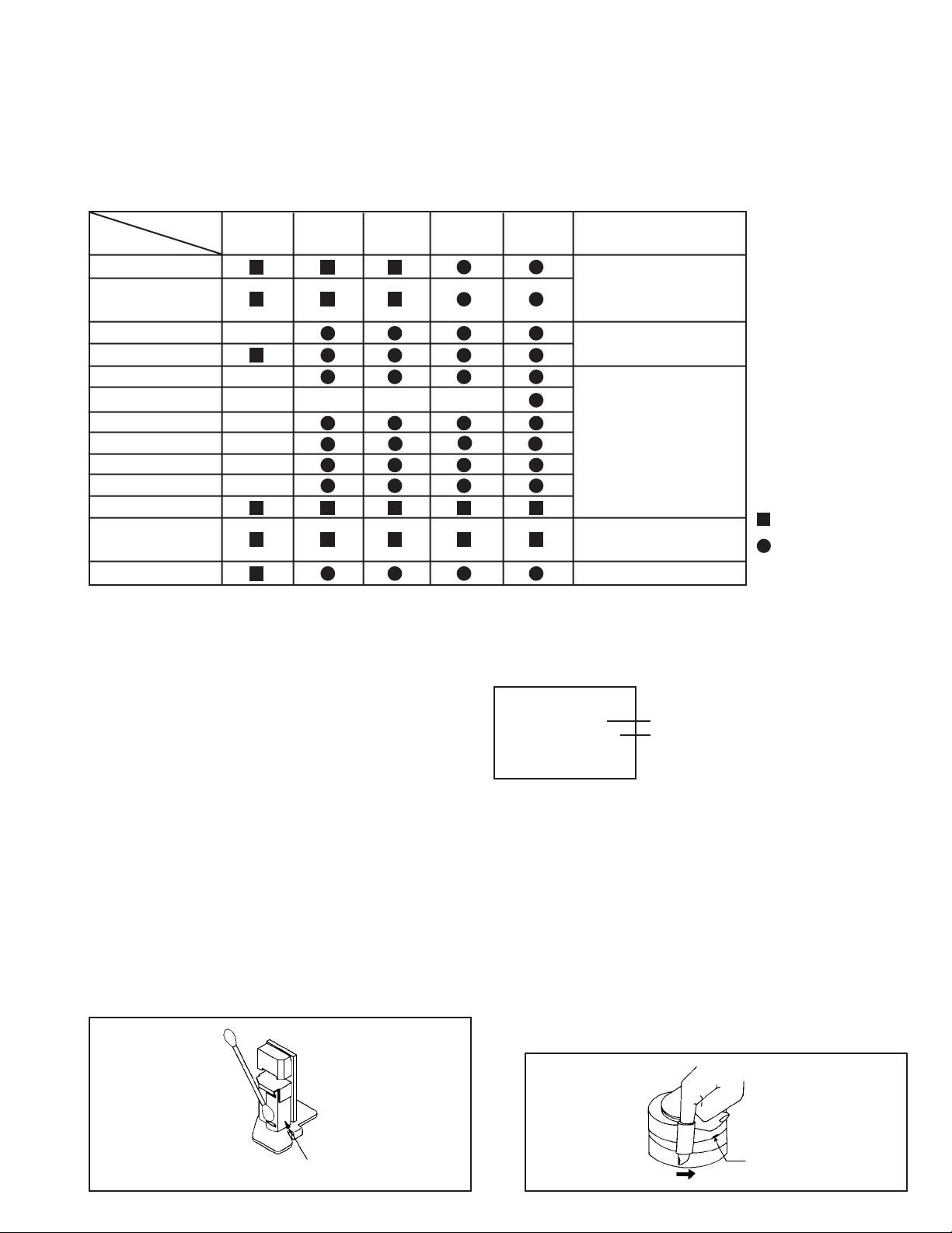
3. CYLINDER
Wrap a piece of chamois around your finger. Dip it in
isopropyl alcohol. Hold it to the cylinder head softly.
Turn the cylinder head counterclockwise to clean it (in the
direction of the arrow). (Refer to the figure below.)
NOTE
Do not exert force against the cylinder head. Do not move
the chamois upward or downward on the head.
Use the chamois one by one.
Cylinder Head
1-15
Page 20
SERVICING FIXTURES AND TOOLS
(4 heads model)
VHS Alignment Tape
MHP
Torque Tape Short Jumper
Torque Gauge
PUJ48075-2
MECHANISM ADJUSTMENT PARTS LOCATION GUIDE
Roller Driver
PTU94002-2
X-JG153 X Value Adjustment
Screwdriver
4
5
6
3
2
1
10
Tension Connect
1.
T ension Arm
2.
Guide Roller
3.
Audio/Control Head
4.
X value adjustment driver hole
5.
P4 Post
6.
T Brake Spring
7.
T Reel
8.
S Reel
9.
Adjusting section for the Tension Arm position
10.
89
7
1-16
Page 21
MECHANICAL ADJUSTMENTS
TAPE REMOVAL METHOD AT NO POWER SUPPLY
1.
Remove the Top Cabinet, Front Cabinet and DVD Block.
(Refer to item 1 of the DISASSEMBLY INSTRUCTIONS.)
2.
Remove the screw 1 of the Deck Chassis and remove the
Loading Motor. (Refer to Fig. 2)
3.
Rotate the Pinch Roller Cam in the direction of the arrow by
hand to slacken the Video Tape.
4.
Rotate the Clutch Ass'y either of the derections to wind the
Video Tape in the Cassette Case.
5.
Repeat the above step 3~4. Then take out the Video
Cassette from the Deck Chassis.
Be careful not to scratch on the tape.
Loading Motor
Screw 1
Capstan DD Unit
Pinch Roller Cam
Main Cam
Clutch Ass'y
1. CONFIRMATION AND ADJUSTMENT
Read the following NOTES before starting work.
• Place an object which weighs between 450g~500g on the
Cassette Tape to keep it steady when you want to make
the tape run without the Cassette Holder. (Do not place
an object which weighs over 500g.)
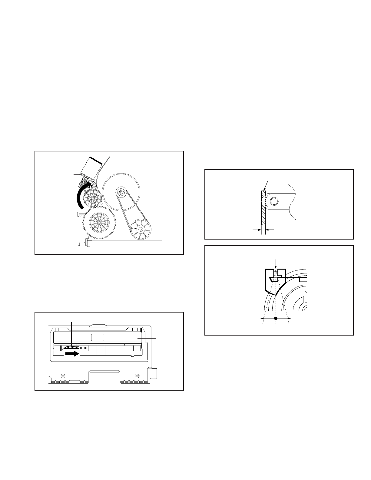
1-1: CONFIRMATION AND ADJUSTMENT OF TENSION
POST POSITION
1.
Set to the PLAY mode.
2.
Adjust the adjusting section for the Tension Arm position
so that the Tension Arm top is within the standard line of
Main Chassis.
3.
While turning the S Reel clockwise, confirm that the edge
of the Tension Arm is located in the position described
above.
Standard line of Main Chassis
T ension Arm
0.5mm (Adjusting range)
Fig. 1-1-A
Main Chassis (Front Side)
DISC REMOVAL METHOD AT NO POWER
SUPPLY
Remove the Top Cabinet and Front Cabinet. (Refer to item
1.
1 of the DISASSEMBLY INSTRUCTIONS.)
Rotate the gear of Deck CD section in the direction of the
2.
arrow by hand, remove the disc from Deck CD.
Gear
Deck CD
Adjusting section for the
Tension Arm position
Tension Band
The Tension Arm top will
move to the inside direction
of the Main Chassis.
Bend
The Tension Arm top will
move to the outside direction
of the Main Chassis.
Fig. 1-1-B
1-2: CONFIRMATION OF PLAYBACK TORQUE AND
BACK TENSION TORQUE DURING PLAYBACK
1.
After confirmation and adjustment of Tension Post
position (Refer to item 1-1), load the cassette type
torque tape and set to the PLAY mode.
2.
Confirm that the right meter of the torque tape indicates
50~90gf•cm during playback in SP mode.
3.
Confirm that the left meter of the torque tape indicates
25~40gf•cm during playback in SP mode.
1-3: CONFIRMATION OF VSR TORQUE
1.2.Install the Torque Gauge on the S Reel. Set to the Picture
Search (Rewind) mode. (Refer to Fig.1-2-B)
Then, confirm that it indicates 120~180gf•cm.
NOTE
Install the Torque Gauge on the reel disk firmly. Press the
REW button to turn the reel disk.
1-17
Page 22
MECHANICAL ADJUSTMENTS
1-4: CONFIRMATION OF REEL BRAKE TORQUE
(S Reel Brake) (Refer to Fig. 1-2-B)
1.
Once set to the Fast Forward mode then set to the Stop
mode. While, unplug the AC cord when the Pinch Roller
Block is on the position of Fig. 1-2-A.
2.
Move the Idler Ass’y from the S Reel.
3.
Install the Torque Gauge on the S Reel. Turn the Torque
Gauge clockwise.
4.
Then, confirm that it indicates 60~100gf•cm.
(T Reel Brake) (Refer to Fig. 1-2-B)
1.
Once set to the Fast Forward mode then set to the Stop
mode. While, unplug the AC cord when the Pinch Roller
Block is on the position of Fig. 1-2-A.
2.
Move the Idler Ass’y from the T Reel.
3.
Install the Torque Gauge on the T reel. Turn the Torque
Gauge counterclockwise.
4.
Then, confirm that it indicates 30~50gf•cm.
The position at FF mode.
Pinch Roller Block
Stop at this position.
The position at
STOP mode.
Capstan DD Unit
Cassette Holder Ass’y
Cassette Opener
Fig. 1-2-A
2. CONFIRMA TION AND ADJUSTMENT OF TAPE RUNNING MECHANISM
Tape Running Mechanism is adjusted precisely at the
factory. Adjustment is not necessary as usual. When you
replace the parts of the tape running mechanism because of
long term usage or failure, the confirmation and adjustment
are necessary.
2-1: GUIDE ROLLER
1.
Playback the VHS Alignment Tape (MHP).
2.
Connect CH-1 of the oscilloscope to TP101 (Envelope)
and CH-2 to TP3002 (SW Pulse).
3.
Press and hold the Tracking-Auto button on the remote
control more than 2 seconds to set tracking to center.
4.
Trigger with SW Pulse and observe the envelope. (Refer
to Fig. 2-1-A)
5.
When observing the envelope, adjust the Roller Driver
(PTU94002-2) slightly until the envelope will be flat.
Even if you press the Tracking Button, adjust so that
flatness is not moved so much. (Refer to Fig. 2-1-B)
6.
Adjust so that the A : B ratio is better than 3 : 2 as shown
in Fig. 2-1-C, even if you press the Tracking Button to
move the envelope (The envelope waveform will begin to
decrease when you press the Tracking Button).
7.
Adjust the PG shifter during playback.
(Refer to the ELECTRICAL ADJUSTMENTS)
NOTE
After adjustment, confirm and adjust A/C head.
(Refer to item 2-2)
Torque Gauge
Torque Gauge
S Reel
T Reel
Fig. 1-2-B
NOTE
If the torque is out of the range, replace the following parts.
Check item
1-3
1-4
S Reel side:
Replacement Part
Idler Ass’y/Clutch Ass’y
S Reel/Tension Band/Tension
Connect/Tension Arm Ass’y
T Reel side:
T Reel/T Brake Band//T Brake
Spring/T Brake Arm
CH-1
Envelope
(TP101)
CH-2
SW Pulse (TP3002)
Improper Proper
(a) Guide roller
(b) P4 Cap
Entrance
Max
A B
CH-1
CH-2
Track
Track
A : B ≥ 3 : 2
Fig. 2-1-A
Fig. 2-1-B
Exit
Max
Fig. 2-1-C
1-18
Page 23
MECHANICAL ADJUSTMENTS
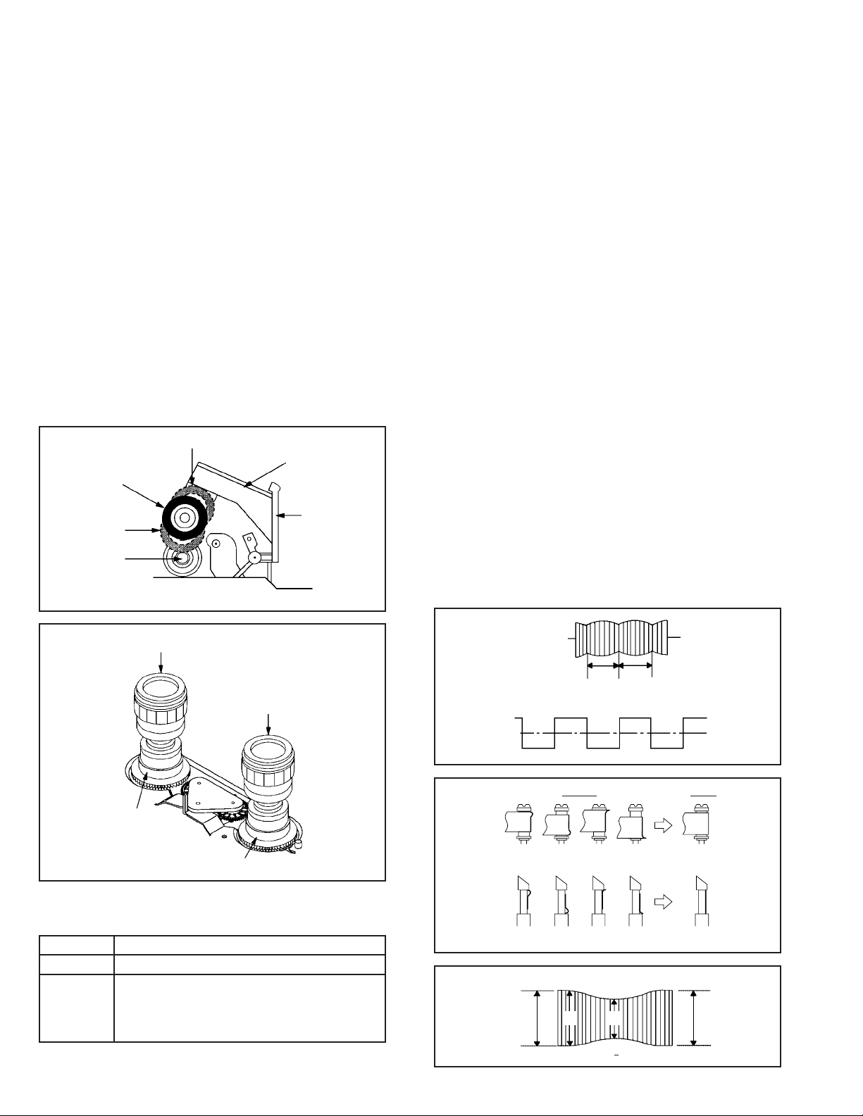
2-2: CONFIRMATION AND ADJUSTMENT OF AUDIO/
CONTROL HEAD
When the Tape Running Mechanism does not work well,
adjust the following items.
1.
Playback the VHS Alignment Tape (MHP).
2.
Confirm that the reflected picture of stamp mark is
appeared on the tape prior to P4 Post as shown in Fig. 2-
2-A.
a)
When the reflected picture is distorted, turn the screw
1 clockwise until the distortion is disappeared.
b)
When the reflected picture is not distorted, turn the
screw 1 counterclockwise until little distortion is
appeared, then adjust the a).
3.
Turn the screw 2 to set the audio level to maximum.
4.
Confirm that the bottom of the Audio/ Control Head and
the bottom of the tape is shown in Fig. 2-2-C.
c)
When the height is not correct, turn the screw 3 to
adjust the height. Then, adjust the 1~3 again.
Audio/Control Head
Reflected picture of
Stamp Mark
P4 Cap
2-3: TAPE RUNNING ADJUSTMENT
(X VALUE ADJUSTMENT)
1.
Confirm and adjust the position of the Tension Post.
(Refer to item 1-1)
2.
Adjust the Guide Roller. (Refer to item 2-1)
3.
Confirm and adjust the Audio/Control Head.
(Refer to item 2-2)
4.
Connect CH-1 of the oscilloscope to TP3002, CH-2 to
TP101 and CH-3 to Audio Out.
5.
Playback the VHS Alignment Tape (MHP).
6.
Press and hold the Tracking-Auto button on the remote
control more than 2 seconds to set tracking to center.
7.
Set the X Value adjustment driver (X-JG153) to the 4 of
Fig. 2-2-B. At first, tur n the Audio/Control Head position
fully toward the capstan side. Then adjust X Value to turn
it back gradually toward the cylinder side and stop on the
second peak point position of the envelope.
Play MHP
Waveform output
X-value adjustment point
Drum side Control head position Capstan side
Audio/Control Head
3
2
Audio/Control Head
Tape
Stamp Mark
1
4
Fig. 2-2-A
Fig. 2-2-B
0.25±0.05mm
Fig. 2-2-C
Maximum
8.
Perfor m tracking operation and confirm the envelope is
maximum on the tracking center position.
9.
Playback the VHS Alignment Tape (MHP-L).
10.
Perfor m tracking operation and confirm the envelope is
maximum on the tracking center position. If envelope is
not maximum, should be fine-tune the X-VALUE.
Fig. 2-3
1-19
Page 24
ELECTRICAL ADJUSTMENTS
Read and perform this adjustment when repairing the
circuits or replacing electrical parts or PCB assemblies.
1. BASIC ADJUSTMENT
CAUTION
When you exchange IC and Transistor for a heat sink,
apply the silicon grease (YG6260M) on the contact section
of the heat sink. Before applying new silicon grease,
remove all the old silicon grease. (Old grease may cause
damages to the IC and Transistor.)
1-1: SWITCHING POINT
CONDITIONS
MODE-PLAYBACK
Input Signal-Alignment Tape (MHP)
INSTRUCTIONS
Connect CH-1 on the oscilloscope to TP3002 and CH-2
1.
to TP8001.
Playback the alignment tape. (MHP)
2.
Press and hold the Tracking-Auto button on the remote
3.
control more than 2 seconds to set tracking to center.
Press both CH UP button on the set and the STOP button
4.
on the set for more than 2 seconds.
CH-2
6.5H
CH-1
Fig. 1-1-A
CH-2
CH-1
6.5H
Fig. 1-1-B
ELECTRICAL ADJUSTMENT PARTS LOCATION GUIDE (Connector Connections)
TU301
TP3001
TP3002
CP103
J8003
TP8001
TP101
J8001
FE HEAD
J8005
J8004
J8007
OS8001
J8006
CP102
CD102
AC HEAD
OPERATION PCB
SW7001
J8008
OS651
VCR/DVD PCB
CP681
V651
CD681
CP2601
CP2301
CP2302
CP651
CD501
CD2302
AC IN
CD2601
CD2301
1-20
TP101
TP3001
TP3002
TP8001
:
Envelope
:
Service Mode
:
Switching Pulse
:
Switching Point
DECK CD
Page 25

IC DESCRIPTIONS
VCR/DVD PCB OEC0132A (IC3001)
No. PORT PIN NAME I/O DESCRIPRION
1 SVSS SVSS - Ground.
2 CTL_REF CTL_REF Output terminal for CTL amp REF (1/2 SVCC)
3 CTL-H(+) CTL-H(+) Input and output terminal of Control Head.
4 CTL-H(-) CTL-H(-) Input terminal of Control Head.
5 CTL_BIAS CTL_BIAS Output terminal for bias.
6 CTL_FB CTL_FB Input terminal for CTL feedback
7 CTL_AMP(O) CTL_AMP(O) Output terminal for amp out.
8 CTL_AMP(I) CTL_AMP(I) Input terminal for CTL shumit amp .
9 CFG CFG Input terminal for CAPSTAN FG signal detection.
10 SVCC SVCC + 5V (Servo)
11 AFC_PC AFC_PC AFC oscilator (external circuit).
12 AFC_OSC AFC_OSC AFC oscilator (external circuit).
13 AFC_LPF AFC_LPF LPF connection for AFC OSC.
14 CSYN/HSYN CSYNC OUT Output terminal for composite SYNC.
15 VLPF/VSYN VSYNC IN Input terminal for composite SYNC.(from 14pin)
16 CV_IN2 CV_IN2 IN Composite Video input terminal.(for data slicer)
17 CV_IN1 CV_IN1 IN Composite Video input terminal.(for OSD)
18 OSD VCC OSDVCC - + 5V
19 CV_OUT CV_OUT OUT Composite Video output.(with OSD)
20 OSD_VSS OSD_VSS - Ground.
21 4/2 FSC_OUT 4/2 FSC_OUT OUT 4 FSC pulse.
22 4/2 FSC_IN 4/2 FSC_IN IN 4 FSC pulse.
23 AVSS AVSS - Ground.
24 AN-B VIDEO_ENV IN Input terminal of video RF envelope.
25 AN-A BOT-H IN Tape start sensor input signal.
26 AN-9 EOT-H IN Tape end sensor input signal.
27 AN8 MS_SEN-B IN Input terminal of mecha state sensor.
28 P07/AN7 MS_SEN-A IN
29 P06/AN6 KEY-B IN Main unit key input.
30 P05/AN5 KEY-A IN
31 P04/AN4 STEREO_SEL IN Input terminal for the judgement of voice reception condition.
32 P03/AN3 HI-FI_ENV IN Input terminal of HiFi RF envelope.
33 P02/AN2 AFT-S_CURVE IN AFT S CURVE input for tuner.
34 P01/AN1 SERVICE IN Input terminal for Service Mode.
35 P00/AN0 TAB SW IN Input terminal for judge the tape if it has TAB or not.
36 AVCC AVCC - ON/OFF control Micon AD section.
37 P10/IRQ0 POWER_FAIL IN Input terminal of Power fail signal.
38 P11/IRQ1 VIDEO MUTE H OUT H for at AUTO_CLOCK in POWER OFF.
39 P12/IRQ2 POWER ON L OUT For control the user power switch ON/OFF.
1-21
Page 26

IC DESCRIPTIONS
VCR/DVD PCB OEC0132A (IC3001)
40 P13/IRQ3 REEL-S IN Input terminal of reel sensor supply.
41 P14/IRQ4 REEL-T IN Input terminal of reel sensor take up.
42 P15/IRQ5 POWER ON-H OUT For control the user power switch ON/OFF.
43 P16/IC REM_IN IN Receive the remote control signal.
44 P17/TMOW DVD RESET OUT For control the DVD RESET.
45 P67/RP7/TMB DVD POWER CTL OUT Output terminal for DVD power CTL.(3.3V/9V)
46 P66/RP6/ADTRG DVD LED OUT The DVD LED light-up/put-off control output.
47 P65/RP5 VCR LED OUT The VCR LED light-up/put-off control output.
48 P64/RP4 1G/T-REC LED OUT LEM(LED Module) control terminal.
49 P63/RP3 2G/REC LED OUT LEM(LED Module) control terminal.
50 P62/RP2 3G/TV/VCR LED OUT LEM(LED Module) control terminal.
51 P61/RP1 4G OUT LEM(LED Module) control terminal.
52 P60/RP0 5G OUT LEM(LED Module) control terminal.
53 P37/TM0 Y/C CLOCK OUT Control terminal for Y/C. (CLOCK).
54 P36/BUZZ Y/C DATA OUT Control terminal for Y/C.(DATA).
55
56 VCC VCC - Power of CPU.
57 VSS VSS - Ground.
58
59
60 P25 SEG4 OUT LEM(LED Module) control terminal.
61 P24/SCL1 IIC CLK OUT CLOCK terminal for IIC BUS communication.
62 P23/SDA1 IIC DATA OUT DATA terminal for IIC BUS communication.
63 P22/SCK1 SEG5 OUT LEM(LED Module) control terminal.
64 P21/SO1 SO1/TX OUT Input terminal for DVD communication.(asynchronous)
65 P20/SI1 SI1/RX IN Output terminal for DVD communication.(asynchronous)
66 P47/RPTRG SEG6 OUT LEM(LED Module) control terminal.
67 P46/FTOB SEG7 OUT LEM(LED Module) control terminal.
68 P45/FTOA SEG8 OUT LEM(LED Module) control terminal.
69 P44/FTID NC OUT Not used.
70 P43/FTIC NC OUT Not used.
71 P42/FTIB SEG9 OUT LEM(LED Module) control terminal.
72 P41/FTIA NC OUT Not used.
73 P40/PWM14 SEG10 OUT LEM(LED Module) control terminal.
74 FEW FEW IN FZTAT Write protect.
75 X2 X2 OUT Subclock pulse(32.768KHz)
76 X1 X1 IN
77 /RESET /RESET IN RESET will be done when the voltage goes to HIGH after the
78 OSC1 OSC1 IN Connect the main crystal(10MHz)
P35 SEG1 OUT
P27 SEG2 OUT
P26 SEG3 OUT
LEM(LED Module) control terminal.
LEM(LED Module) control terminal.
LEM(LED Module) control terminal.
reset signal.
1-22
Page 27

IC DESCRIPTIONS
VCR/DVD PCB OEC0132A (IC3001)
79 VSS VSS - Ground.
80 OSC2 OSC2 OUT Connect the main crystal(10MHz)
81 VCL VCL IN Connect the capacitor
82 MD0 MD0 IN FZTAT Write MODE.
83 P34/PWM2 NC OUT not used.
84 P33/PWM1 CAP_LIMIT OUT Switch the maximum output current of the Capstan Motor.
85 P32/PWM0 TUNER AUDIO MUTE-H OUT Output low at tuner and output high at external input/play.
86 P31/SV2 VCR-H OUT H for at PLAY in VCR MODE. L for except above case.
87 P30/SV1 POWER_MUTE OUT audio mute at POWER ON/OFF.
88 P70/PPG0 SYS_MUTE OUT audio mute for DVD at POWER ON/OFF.
89 P71/PPG1 NC OUT Not used.
90 P72/PPG2 NC OUT Not used.
91 P73/PPG3 AV SW_2 OUT Control rear/front video signal.(at AV X 2)
92 P74/PPG4/RP8 AV SW_1 OUT Control DVD/VCR video/audio signal.
93 P75/PPG5/RP9 Y/C CS OUT Control terminal for Y/C. (CHIP SELECT).
94 P76/PPG6/RPA RF CH SW OUT 3/4 ch Selection for the RF CH.
95 P77/RPG7/RPB AUDIO_MUTE-H OUT L for at AUDIO MUTE and POWER OFF. H for except above case.
96 P80/YCO V_REC_ST-H OUT On control of A/V recording(Whole width erase) circuit.
97 P81/EXCAP/YBO LDM CTL OUT Loading motor control terminal.
98 P82/EXCTL CAP_FWD-H OUT Capstan forward and backward command.
99 P83/C,ROT/R C.ROTARY OUT Color Rotary Control output.
100 P84/H.AMP/SW/G H.AMP.SW OUT Switching output of Head Amp SW.
101 P85/COMP/B COMP IN Comparison results input of Playback Envelope level on SP/LP
heads (4 heads).
102 P85/EZTTRG CAP_FULL OUT Output the HIGH during the acceleration force of capstan motor at
SLOW mode.
103 P87/DPG CYL_SPEED_UP OUT Output terminal for correct cylinder during SLOW.
104 DFG D FG/PG IN Input terminal for DRUM FG signal detection.
105 VIDEO_FF VIDEO_H.SW OUT Output terminal of Video Head SW.
106 AUDIO_FF HI-FI H.SW OUT Output terminal of HI-FI Head SW.
107 DRUM_PWM DRUM_PWM OUT PWM output of Cylinder control.
108 CAP_PWM CAP_PWM OUT PWM output of Capastan control.
109 V-PULSE DUMMY_V-SYNC OUT Virtual V Pulse output.
110 SV VSS SV VSS - Ground.
111 C.SYNC_IN SYNC IN Input terminal for composite SYNC.
112 VCC VCC(SV) - + 5V
1-23
Page 28
VCR/DVD PCB IC3001 (OEC0132A)
DPG 104 PIN
DFG 104 PIN
SERVO TIMING CHART
24 Cycle
H. SW. P 105 PIN
V-SYNC (E-E) 111 PIN
REC CTL (REC)
7 PIN
V-SYNC (TRICK PB)
109 PIN
• WAVEFORM CHANGES DEPENDED ON THE TAPE SPEED
CH 1
CH 2
1-24
Page 29
C
Y
MECHANISM TIMING CHART
Please see the list below for the operational timing and the mode sensor output of the main parts on each mechanism modes.
MECHANISM MODE UNLOAD STOP3
Mode Dealing
Directions
Revolutional Angle of
MAIN CAM
Moving Quantity of
MAIN ROD (mm)
MODE MS-1
SENSOR
HIGH
LOW
EJECT
0
STBY
15
3
206.3100
180
Output
HIGH
MS-2
LOW
INCLINED BASE S/T UNIT
PINCH ROLLER BLOCK
P5 ARM ASS'Y (T BRAKE:LOW)
TENSION LEVER
TENSION ARM ASS'
(S REEL BRAKE)
VSR
S BRAKE:LOW
255
26.5
PRESS
PRESS
P5-ON (T BRAKE HIGH)
BRAKE-ON
PBF.SLOW
S BRAKE:HIGH
FF/REWSTOP2
323.8303.7272.2226.4
38.53529.521.5
TENSION CONNECT
(S REEL BRAKE)
T BRAKE ARM
(T REEL BRAKE)
LUTCH LEVER
LINK UNIT
FLAP LEVER
BRAKE-ON
BRAKE-ON
CLUTCH-ON
UP
BRAKE-ON
DIRECT
PRESS
1-25
Page 30
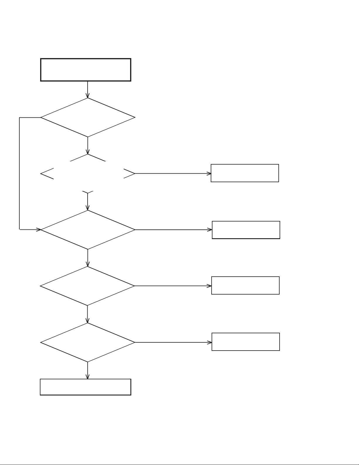
(VCR SECTION)
POWER DOES NOT TURN ON
TROUBLESHOOTING GUIDE
Does display light?
YES
Is the voltage at
pin 30 of IC 3001
0V?
YES
Check of T501
and peripheral circuit.
NO
NO
Is the voltage
linked to L506?
YES
Check of V651
and peripheral circuit.
NO
Check of T501
and peripheral circuit.
Check IC3001.
1-26
Page 31

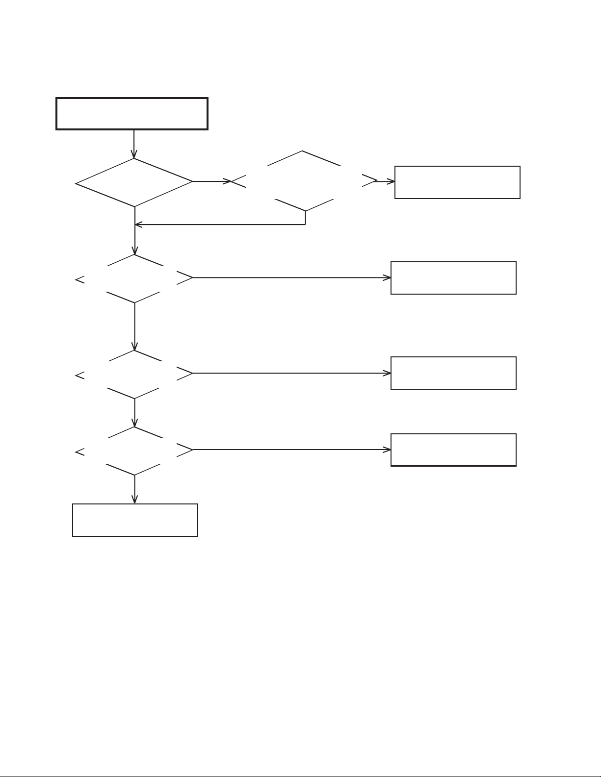
THE POWER SUPPLY CUT
Inserting a casette
and push play button.
TROUBLESHOOTING GUIDE
Does the power cut
after 3 seconds?
NO
Does the power cut
after about 6 seconds?
NO
Check the POWER BLOCK.
YES
YES
Check CAPSTAN DD UNIT
and CYLINDER UNIT.
Check Q3006,Q3008
and CAPSTAN BELT.
1-27
Page 32

AUDIO SHAKES
TROUBLESHOOTING GUIDE
Is AUDIO HEAD
scratched?
NO
At playback,is input about
4.5Vp-p of a rectangular
wave at pin 9 of IC3001?
YES
At playback,is pin 32 of
CP3001 3.5V?
YES
Check AUDIO BLOCK.
YES
NO
NO
Change AUDIO HEAD.
Change CAPSTAN DD UNIT.
Check IC3001.
1-28
Page 33

The CASSETTE TAPE
CAN NOT BE INSERTED
TROUBLESHOOTING GUIDE
Does WORM GEAR of
cassette loading block
move?
YES
When a CASSETTE can
not inserted, is pin 25 of
IC3001 5V ?
YES
When a CASSETTE is
inserted, is pin 8 of
CP3001 12.6V ?
NO
Check circuit of POWER BLOCK.
NO
NO
YES
Check WORM GEAR
of cassette loading block.
Check LED of DECK,
PHOTO SENSOR.
Change
LOADING MOTOR.
1-29
Page 34

CAN NOT FF/REW
TROUBLESHOOTING GUIDE
At FF/REW, does voltage
at pin98 of IC3001
change?
YES
Check DECK MECHANISM.
WHEN INSERTING A CASSETTE,
IT EJECTS IMMEDIATELY
Does another CASSETTE
insert?
YES
NO
NO
Check of IC3001.
Defective CASSETTE
or cassette loading block.
1-30
Does SW3001 and
REC LEVER
correctly set ?
YES
After inserting
CASSETTE, is pin 35
of IC3001 0V ?
YES
Check IC3001.
NO
NO
Correctly SW3001
and REC LEVER set.
Check SW3001.
Page 35

TAPE LOADING IS OK, BUT
UNLOADS IMMEDIATELY
TROUBLESHOOTING GUIDE
Does CYLINDER
rotate?
YES
Is there HEAD SW
PULSE at TP3002.
YES
NO
NO
Is the voltage
at pin 2 of CP3001
12V ?
YES
At play, is the voltage
at pin 12 of CP3001 2.6V ?
YES
Change CYLINDER unit.
NO
Is PG PULSE signal
inputted to pin 104
of IC3001 ?
YES
NO
NO
Check POWER BLOCK.
Check Q3006 and Q3008.
Change IC3001.
1-31
Page 36

AT PLAY, THE PICTURE
JITTERS VERTICAL MINUTELY
TROUBLESHOOTING GUIDE
Is FG wave of CP3001
at pin 11 5V ?
5V
YES
Is pin 12 of CP3001 2.6V ?
YES
Change CYLINDER MOTOR.
AUTO TRACKING
DOES NOT OPERATE
In auto tracking, is the
voltage at pin 24 of IC3001
more than DC 0.2V?
NO
NO
NO
Does the CTL pulse
signal (about 2.5Vp-p)
appear at pin 7 of IC3001.
2.5Vp-p
NO
Change
CYLINDER MOTOR.
Change IC3001.
Check CONTROL HEAD.
Change IC3001.
1-32
YES
YES
Page 37

WHEN PLAYBACK, FF OR REW
MODE IS ACTIVE, UNIT STOPS
IMMEDIATELY
TROUBLESHOOTING GUIDE
Does CAPSTAN DD
MOTOR rotate?
YES
Is there REEL SENSOR
PULSE signal at pin 40
and pin 41 of IC3001.
YES
Change IC3001.
NO
NO
Refer to section "CAPSTAN
DD MOTOR NOT
ROTAING".
Check Q3001 and Q3002.
1-33
Page 38
TROUBLESHOOTING GUIDE
AT PLAY, PICTURE JITTERS
HORIZONTALLY
NO
Does a noise on the picture
appear?
YES
By adjusting the MANUAL
TRACKING UP/DOWN
BUTTONS, will the line
disappear?
YES
Is a height of GUIDE POST
maximum?
YES
Is PG SHIFTER
adjustment 6.5H?
NO
NO
NO
Check P/B ENVELOPE.
The height of GUIDE POST
readjust.
Adjust PG SHIFTER.
1-34
YES
Is a wave of PB-Y unusual?
YES
Change IC101.
NO
Change IC101
and peripheral circuit.
Page 39
AT PLAYBACK, THE PICTUER
DOES NOT APPEAR
TROUBLESHOOTING GUIDE
Does E-E picture
appear?
YES
Is there video signal
of IC101 at pin 26?
YES
Is there video signal
of IC8005 at pin 7?
YES
Is there video signal of
IC101 at pin 26?
NO
NO
NO
NO
Is the voltage of IC101 at
pin 44, 45, 52 and 68 5V?
YES
NO
Check POWER BLOCK.
Change IC101.
Change IC8005.
Change IC101.
YES
Check J8001.
1-35
Page 40

AT PLAYBACK, THE COLER DOES
NOT APPEAR
TROUBLESHOOTING GUIDE
Is there color signal in
video signal at pin 26 of
IC101.
YES
NO COLER DURING SELF
RECORDING AND PLAYBACK
Is there CHROMA signal at
pin 30, 32 of IC101.
YES
NO
NO
Is there video signal at pin
26 of IC101.
YES
Change IC101.
NO
Check TU301, J8003,
circuit around it.
Change X'tal.
Is there CHROMA signal at
pin 26 of IC101.
YES
Check circuit around of J8001.
1-36
NO
Change IC101.
Page 41

AT PLAYBACK AND RECORDING,
CYLINDER MOTOR UNLOAD
TROUBLESHOOTING GUIDE
Is the voltage at pin 8 of
CP3001 about DC12.6V?
YES
In playback,is at pin 12 of
CP3001 about DC2.6V?
YES
Check the DECK BLOCK.
PLAYBACK PICTURE IS NOISY
(EVEN AFTER CLEANING HEADS)
NO
NO
Check IC502.
Check IC3001.
Is noisy a wave of video
signal at pin 26 of IC101?
YES
Is noisy a wave of video signal
of EMITTER of Q8004
NO
Check J8001.
NO
YES
Check CYLINDER.
Check Q8004.
1-37
Page 42

AT PLAY, AUDIO DOES NOT
APPEAR
TROUBLESHOOTING GUIDE
At E-E, does audio appear?
YES
Is the voltage at pin 6 of
IC101 about 2.5V?
YES
Is there audio signal at pin
10 of IC101?
YES
Is there audio signal at pin
22, 24 of IC701?
NO
NO
NO
YES
Refer to section"E-E DOES
NOT APPEAR".
Check A/C HEAD.
Check circuit around at pin
10 of IC101.
Check circuit around at pin
22, 24 of IC701.
NO
Check whether there are not a
damage, dirt in AUDIO HEAD.
1-38
Page 43

THE AUDIO CAN NOT
RECORD
TROUBLESHOOTING GUIDE
Is bias level at L101 OK?
YES
Is there audio signal at
pin 76, 78 and 80 of IC101?
NO
NO
In starting recording,
is there sine wave at
pin 11 of IC101?
YES
Check disconnection
and short of L101.
NO
Check POWER BLOCK and
voltage of base of Q103.
Check IC701 and
the circuit from TUNER
or audio input juck to IC701 .
YES
Is there voltage
of base of Q103
about 5V?
YES
Is there Asine wave
at pin 5 of L101?
YES
Check lead wire of A/C HEAD
and CONNECTOR.
NO
NO
Change Q103.
Change L101.
1-39
Page 44
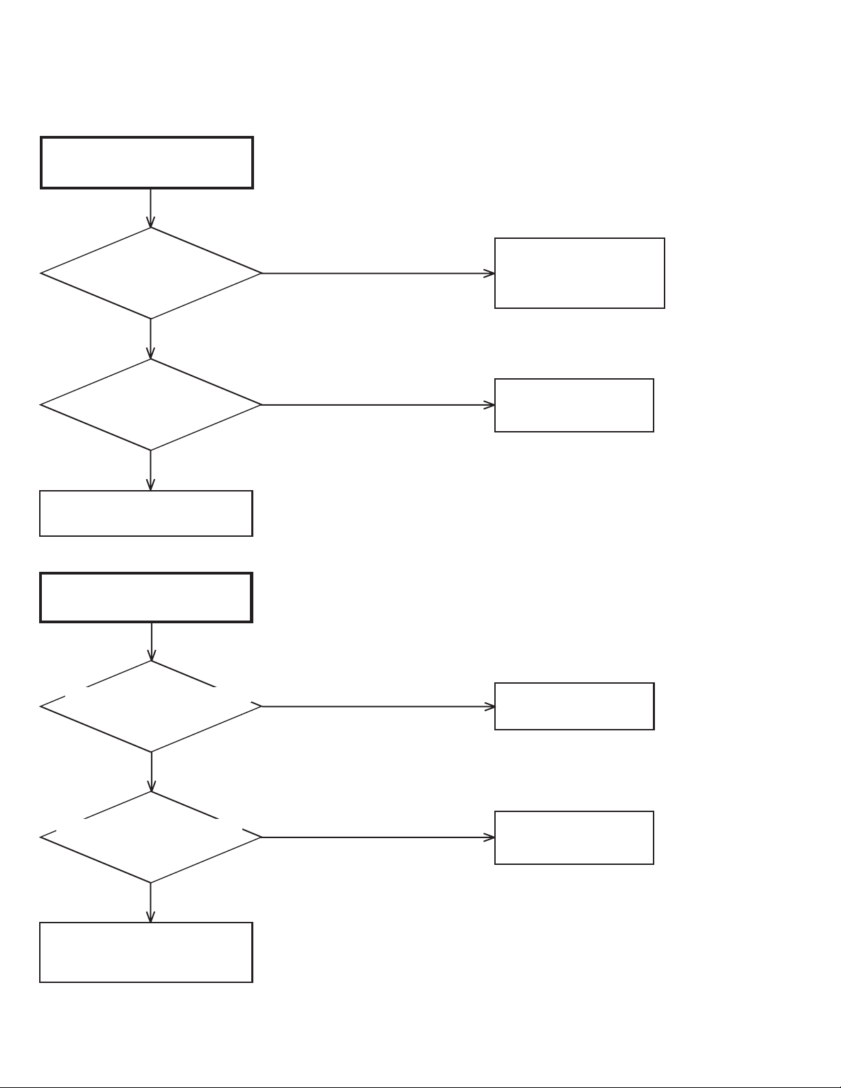
THE CASSETTE INSERT, BUT
THE TAPE DOES NOT MOVE
TROUBLESHOOTING GUIDE
Does the mode
appear at display?
YES
Does operate with
remote control?
YES
Check operation PCB.
CAPSTAN DD MOTOR NOT
ROTATING
NO
NO
Check LOADING MOTOR and
MODE SENSOR
RELATION DEPARTMENT.
Check IC3001.
In playback,is there voltage at
pin 2 of CP3001 12V?
In playback,is there voltage at
pin 78 of IC3001 2.5V?
DD MOTOR rotate now?
If not, replace it.
1-40
YES
YES
NO
NO
Check POWER BLOCK.
Change IC3001.
Page 45

RECORDING MECHANISM WORKS,
BUT NO VIDEO RECORD FROM
INPUT JACK OR TUNER
TROUBLESHOOTING GUIDE
Is there video signal at
pin 30, 32 of IC 101?
YES
Is the BASE of
Q103 5V?
YES
Is there video signal
at pin 26 of IC101?
NO
NO
NO
Is the voltage at pin 96
of IC3001 5V?
YES
NO
Check cricuit of video signal from
VIDEO IN or
TUNER to IC101.
Change IC3001.
Change IC101.
YES
Check CYLINDER UNIT and
circuit around of CP101.
1-41
Page 46

E-E DOES NOT APPEAR
(THE PICTURE DOES NOT
APPEAR FROM TUNER)
TROUBLESHOOTING GUIDE
Does normality AUDIO JACK
CONNECT?
YES
Are there thevoltage
of +B(5V),TU(32V)
of TU301?
YES
Check the picture.
Is there video signal at
pin 18 of TU301?
NO
NO
NO
Connection is done over again.
Check POWER BLOCK.
Change TU301.
YES
Is there video signal
at pin 26 of IC101?
YES
Is there video signal at
pin 19 of IC3001?
YES
Check J8001.
NO
NO
Change IC101.
Change IC3001.
1-42
Page 47
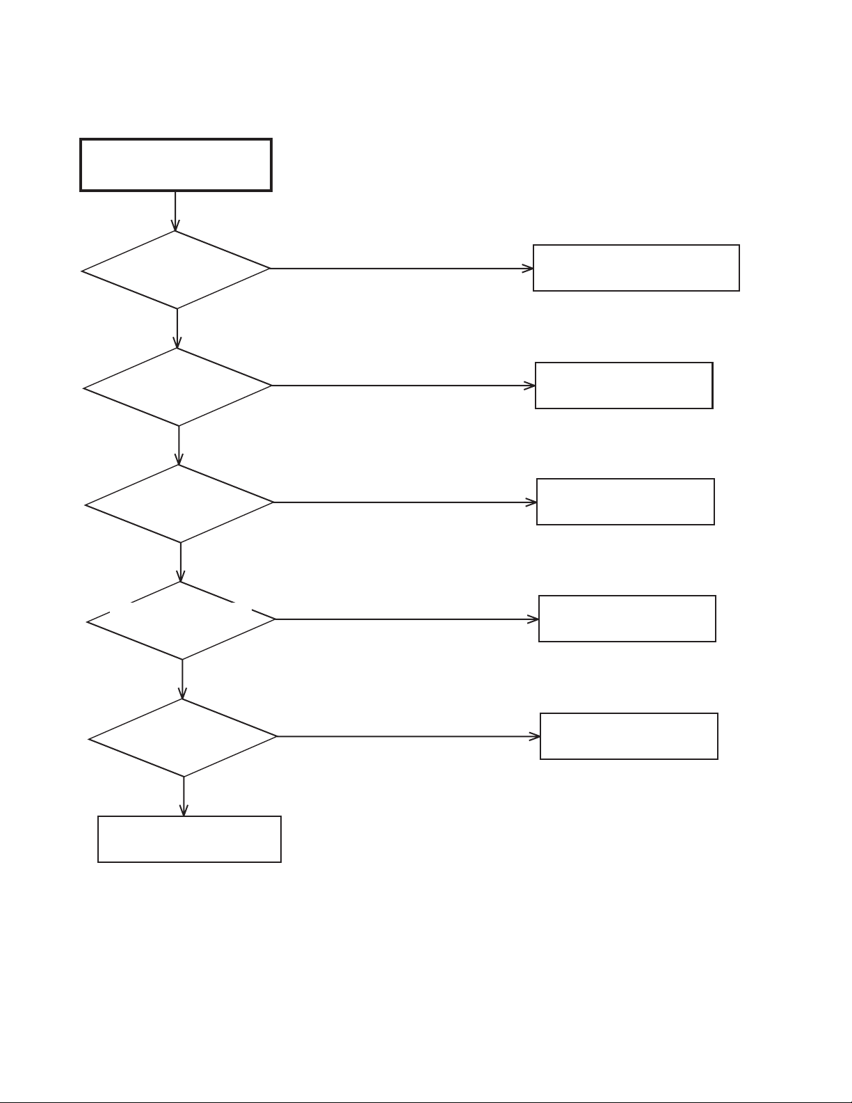
E-E AUDIO (MONO)
DOES NOT APPEAR
TROUBLESHOOTING GUIDE
Does E-E AUDIO
(STEREO) appear?
YES
Is the voltage at pin 7
of IC101 5V?
YES
Is the voltage at pin 95 of
IC3001 5V?
NO
Is there audio signal at
pin 10, 15 of IC701?
NO
NO
YES
NO
Refer to section "E-E AUDIO
(STEREO) DOES NOT APPEAR".
Check POWER BLOCK.
Change IC3001.
Check J8004, J8005.
YES
Is there audio signal at
pin 61 of IC701?
YES
Check circuit around of J8001.
NO
Change IC701.
1-43
Page 48

E-E AUDIO (STEREO)
DOES NOT APPEAR
TROUBLESHOOTING GUIDE
Is the voltage at pin
25,40,51 of IC701 5V?
YES
Is the voltage at pin
58 of IC701 12V?
YES
Is there Audio signal at
pin 10, 15 of IC701?
YES
Is there Audio signal at
pin 53, 57 of IC701.
NO
NO
NO
NO
Check POWER BLOCK.
Check POWER BLOCK.
Check J8004, J8005.
Change IC701.
YES
Check circuit around of J8001.
1-44
Page 49

TUNER AUDIO (MONO)
DOES NOT APPEAR
TROUBLESHOOTING GUIDE
Does E-E AUDIO
(MONO) appear?
YES
Is there signal at pin
48 of IC701?
YES
Is there audio signal at
pin 53, 57 of IC701?
YES
Is there audio signal
a collector of Q8005
and Q8006?
NO
NO
NO
NO
Refer to section "E-E AUDIO
(MONO) DOES NOT APPEAR".
Check circuit around of TU301
at pin 15.
Change IC701.
Check IC701.
YES
Check circuit around of J8001.
1-45
Page 50

TUNER AUDIO (STEREO)
DOES NOT APPEAR
TROUBLESHOOTING GUIDE
Does TUNER AUDIO
(MONO) appear?
YES
Does E-E AUDIO
(STEREO) appear?
YES
At the time of channel
change,does the display of a
stereo come out to the screen?
YES
Is there audio signal at
pin 48 of IC701?
NO
NO
NO
NO
Refer to section "TUNER AUDIO
(MONO) DOES NOT APPEAR".
Refer to section "E-E AUDIO
(STEREO) DOES NOT APPEAR".
Change IC701.
Check ciruit around of TU301.
YES
Is there audio signal at
pin53, 57 of IC701?
YES
Is there audio signal
a collector of
Q8005 and Q8006.
YES
Check circuit around of J8001.
NO
NO
Change IC701.
Check IC701.
1-46
Page 51

PB AUDIO (Hi-Fi)
DOES NOT APPEAR
TROUBLESHOOTING GUIDE
Does E-E AUDIO
(STEREO) appear?
YES
Does NORMAL PB
AUDIO appear?
YES
Is there audio signal at
pin 22, 24 of IC701?
YES
Is there audio signal at
pin 53, 57 of IC701?
NO
NO
NO
NO
Refer to section "E-E AUDIO
(STEREO) DOES NOT APPEAR".
Refer to section "AT PLAY,
AUDIO DOES NOT APPEAR".
Check circuit of HEAD AMP
and CYLINDER UNIT.
Change IC701.
YES
Check circuit around of J8001.
1-47
Page 52
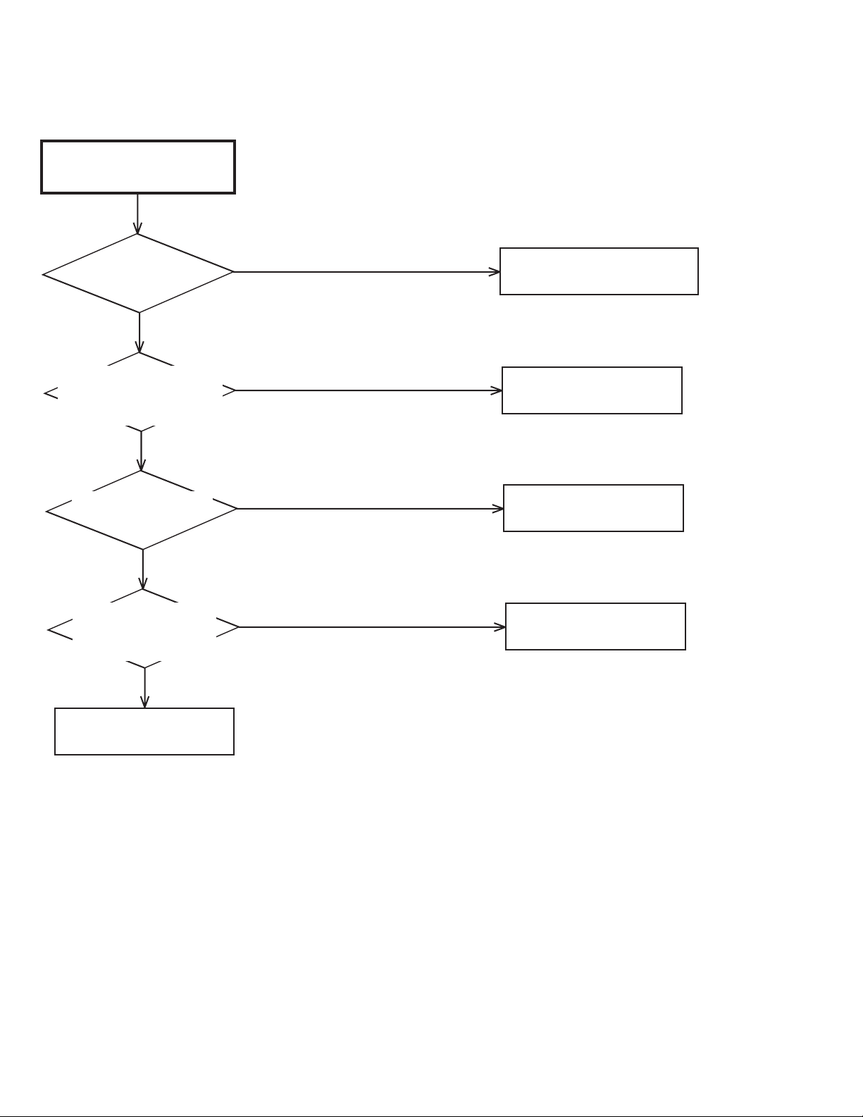
Hi-Fi AUDIO
CAN NOT RECORD
TROUBLESHOOTING GUIDE
Does E-E AUDIO appear?
YES
AT state of video recording,
is there audio signal at
pin 10 and 15 of IC701?
YES
Is there audio signal at
pin 53, 57 of IC701?
YES
At recording and play,is
there signal at pin 7, 8
and 9 of CP101?
NO
NO
NO
NO
Refer to section "E-E AUDIO
(MONO) DOES NOT APPEAR".
Check circuit arounf of J8004,
J8005 and TU301.
Change IC701.
Check CYLINDER UNIT.
YES
Check IC701.
1-48
Page 53

(DVD SECTION)
DECK DOES NOT ACCEPT
OPEN/CLOSE
TROUBLESHOOTING GUIDE
Is the voltage at pin 3 and
14 of IC2301 about DC9V ?
Yes
Is the lose connection
at CD2301 & CD2302 to
DECK ?
No
When AC IN,
DECK MOTOR turn ?
No
Check IC4001 and
peripheral circuit.
No
Yes
Yes
Check P.CON 9V line of
POWER BLOCK.
Check CD2301 & CD2302
connection to DECK.
Check OPEN or SHORT
at Pin 24, 26, 27 and 32
of IC4001.
1-49
Page 54

NO PLAYBACK PICTURE
OF AV JACK
TROUBLESHOOTING GUIDE
Is there VIDEO signal
at pin 170 of IC4001 ?
No
Is the waveform at pins
19~23 of IC4001 ?
Yes
Change IC4001.
NO PLAYBACK PICTURE OF
S-VIDEO JACK
Yes
No
Check IC8005 and peripheral
circuit.
Check IC2001 and peripheral
circuit.
1-50
Is there Y signal at
pin 172 of IC4001 ?
No
Is there VIDEO signal
at pin 170 of IC4001 ?
Yes
Change IC4001.
Yes
No
Check J8006 and peripheral
circuit.
REFER TO "NO PLAYBACK
PICTURE OF AV JACK ".
Page 55

NO COLOR PLAYBACK PICTURE
OF S-VIDEO JACK
TROUBLESHOOTING GUIDE
Is there C signal at
pin 173 of IC4001 ?
No
Is there Y signal at
pin 172 of IC4001?
Yes
Is there VIDEO signal
at pin 170 of IC4001?
No
Is the voltage at pin 28,
83, 130 and 156 of
IC4001 about 1.8V?
Yes
No
Yes
No
Check J8006 and peripheral
circuit.
REFER TO "NO PLAYBACK
PICTURE OF S-VIDEO JACK".
REFER TO "NO PLAYBACK
PICTURE OF AV JACK" .
Check P.CON+3.3V line on
POWER BLOCK.
Yes
Change IC4001.
1-51
Page 56
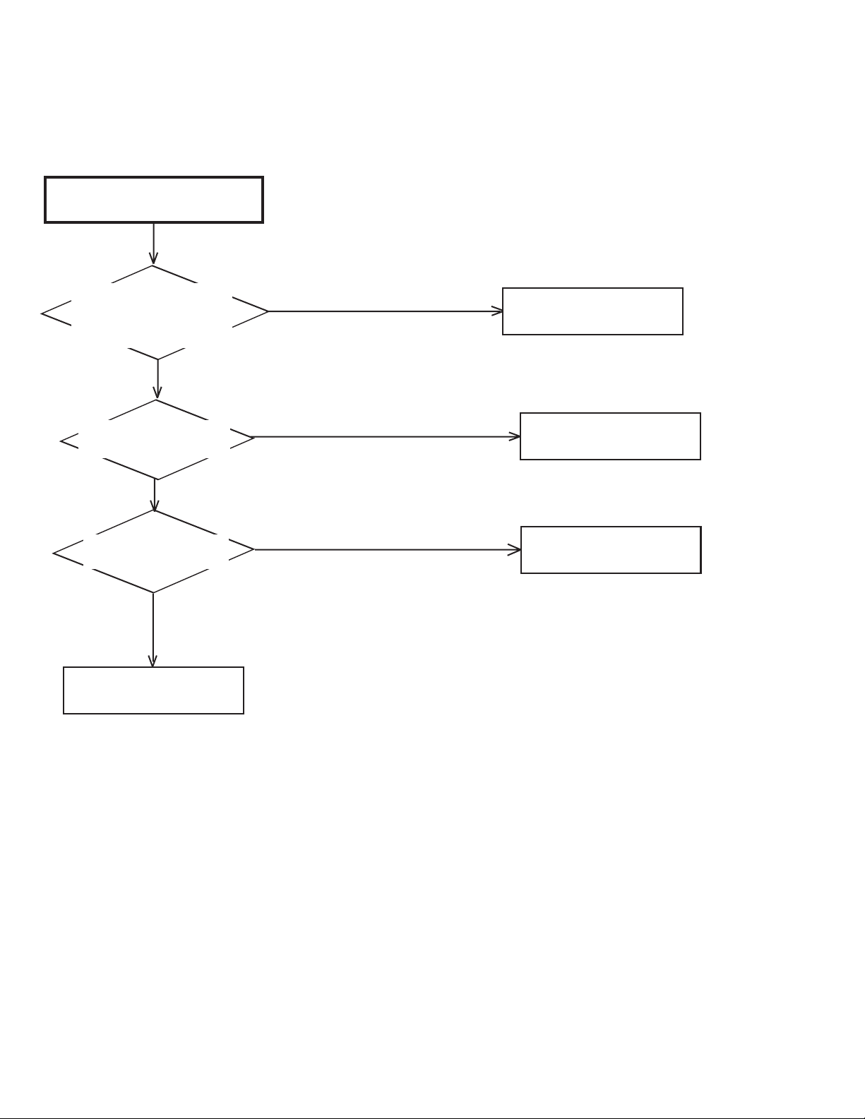
NO AUDIO ON PLAYBACK
TROUBLESHOOTING GUIDE
Is there AUDIO signal at
pin 1 and 7 of IC8003 ?
No
Is there waveform at pin
7 and 8 of IC8004?
No
When DVD Playback , Is
there VIDEO OUTPUT ?
Yes
Change IC4001.
No
Yes
Yes
Check ic8003 and
peripheral circuit.
Check IC8004 and peripheral
circuit.
Check IC2001 and peripheral
circuit.
1-52
Page 57

<Reference>
C
E
C
C
A
SEMICONDUCTOR BASE CONNECTIONS
DIODE
CATHODE
ANODE
1SS133T-77 10ELS6N-TA1B2 1N4005-EIC KDS120RTK MCL4148 LTE-3271T-012A-O
MTZJ13B T-77 21DQ09N-TA2B1 KDS121RTK LTL-1CHGT-002A
MTZJ27B T-77 RGP15J-G23
MTZJ3.0B T-77 RM11C-EIC
MTZJ33B T-77
MTZJ5.1B T-77
MTZJ6.8B T-77
MTZJ9.1B T-77
SARS01-V1
IC
1
1
AN3663FBP LA6560 S-24C02BDP-1A BA10358F-E2 PQ1X251M2ZP KIA431
LA71206M-MPB M11L416256SA-35T S-24C04BFJ-TB NJM2533V(TE2) PS2561L1-1-V(W)
LA9703WL MSM56V16160F-8 NJM4580M PST3231NR
LC78663NRW PCM1742KE/2K
OEC0132A SN74LV4052APW
ZR36742
1 1
1 1
2
3
TRANSISTOR
E
1
4
KIA78R09API PQ070XZ01ZP SST39VF800A-70-4 KTA1241_Y-AT KTC3203_Y-AT 2SA1036KT146
E
C
ST-304L RPI-352C40N STP5NC50FP RPI-303
1
K
E
G
D
S
E
B
KTA1266-AT(Y,GR) KTC3209_Y-AT 2SA1037AKT146
KTA1271_Y-AT KRA101SRTK
G
D
S
B
C
KRA103SRTK
KRC103SRTK
KRC104SRTK
KTA1504S_Y_RTK
KTC3875S_Y_RTK
B
4-1
Page 58

<Reference>
GENERAL SPECIFICATIONS [HR-XVC20US]
G-1 Outline of the product DVD VIDEO PLAYER & VHS Player / Recorder
G-2 DVD System Color System NTSC
G-3 VCR System VHS Player / Recorder
System Video System NTSC
G-4 Tuning Broadcasting System US System M
System Tuner and System 1Tuner
G-5 Power Power Source AC 120V 60Hz
G-6 Regulation Safety UL / CSA
G-7 Temperature Operation 5oC - 40oC
G-8
Operating Humidity
Disc DVD, CD-DA, CD-R/RW, VIDEO CD
Disc Diameter Disc Diameter 120 mm , 80 mm
Deck Disc Loading System Front Disc Loading
Pick up 1-Lens 2-Beams System
Playback time (Max) DVD 1-Layer 135min (4.7GB)
Search speed Fwd 2-20 times / 4 step
Slow speed Fwd 1/7-1/2 times
Hi-Fi STEREO Yes
NTSC PB(PAL60Hz) No
Deck DECK OVD-7
Heads Video Head 4Head
FM Audio Head 2Head
Audio /Control Mono/Yes
T ape Rec P AL Speed NTSC SP/SLP(EP)
Fast Forward / Rewind Time (Approx.) at 25oC FF:1'48"/REW:1'48"
Forward/Reverse NTSC or PAL-M SP/SLP(EP) = 3x,5x / 9x,15x
Picture Search PAL or SECAM Frame Advance Yes
Slow Speed 1/10
Receive CH Destination US (w/CATV)
Intermediate Picture(FP) 45.75 MHz
Frequency Sound(FS) 41.25 MHz
Preset CH RF Converter Output Yes
Stereo/Dual TV Sound US-ST
Tuner Sound Muting Yes
Power Consumption 16 W at 120V 60Hz
Protector Power Fuse Yes
Erase(Full T rac k Erase) Yes
Play PAL -
Channel 3 or 4 ch
Level/Impedance 66 dBu / 75 Ohm
Sound Selector No
Motor 3 Motors
DVD 2-Layer 245min (8.5GB)
CD 74min
VIDEO CD 74min
Actual 2-45 times (DVD, VIDEO CD)
Actual 2-45 times (DVD, VIDEO CD)
Actual -Actual --
Loading System Front
Motor 3
NTSC SP/SLP(EP)
with Cassette T-120
Tuning System F-Synth
Input Impedance VHF/UHF 75 OHM
CH Coverage 2~69,4A,A-5~A-1,A~I
FP-FS 4.50 MHz
DC Stand by 2 W at 120V 60Hz
Per Year -- W
Radiation FCC / IC
Laser DHHS
Storage -20oC - 60oC
4-40 times (CD)
Rev 2-20 times / 4 step
4-40 times (CD)
Rev --
J~W,W+1-W+84
Less than 80% RH
4-2
Page 59

<Reference>
(
)
GENERAL SPECIFICATIONS [HR-XVC20US]
G-9 Signal Video Signal Output Level 1 V p-p/75 ohm (DVD,VCR)
RGB Signal Output Level Audio Signal Input Level Microphone -
Hi-Fi Audio Signal Dynamic Range : More than 90dB
G-10 On Screen
Display (DVD)
Menu
Menu T ype Character
Language Y es
Picture Y es
Sound Y es
Parental Y es
Other Yes
Open Yes
Close Yes
No disc Yes
Reading Yes
Play Yes
Still/Pause Yes
Stop Yes
Prohibit Mark Yes
Step Yes
Next Yes
Back Yes
Random Yes (CD, VIDEO CD, MP3)
Repeat Yes
Slow+ ## Yes
Slow- ## No
Search+ ## Yes
Search- ## Yes
Jump Yes
Resume Yes
Title No. Yes
Chapter No. Yes
Track No. Yes
Time Yes
Sub Title No. Y es
Angle No. Yes
Vocal On/Off Yes
Audio No. Yes
Audio Stereo L/R Yes (VIDEO CD)
Zoom Yes
Marker No. Yes
Spatializer (N-2-2) Yes
Program Play Back Yes (CD, VIDEO CD, MP3)
MP3/WMA/JPEG Folder Name
S/N Ratio (Weighted) 65 dB(DVD) 50 dB(VCR)
Horizontal Resolution 500 Lines (DVD) 230 Lines(VCR Mode)
Input Level Line -8 dBm/ 50k ohm(VCR)
Output Level Line
Digital Output Level 0.5 V p-p / 75 ohm(DVD)
S/N Ratio at (Weighted) 90dB(DVD), 42dB(VCR at SP)
Harmonic Distortion (1KHz) Typical 0.02% (DVD), 1.5% (VCR at SP)
Frequency Response : DVD Mode at DVD 4 Hz - 22 KHz
Frequency Response 20Hz ~20kHz
Wow And Flutter : Less than 0.01 %Wrms
Channel Separation : More than 60 dB
Harmonic Distortion : Less than 0.01
Menu Yes
Sub Title Yes
Audio Y es
TV Screen Size Yes
OSD Display On/Off Yes
Slide Show Yes
Interval Time Y es
DRC (Dynamic Range Control) Yes
dts Decode No
Output (5.1ch/2ch) No
Surround On/Off No
Center On/Off No
Sub Woofer On/Off No
Password Lock/Unlock Yes
Rating Level Yes
OSD Language (Set up Language) Yes
Output (RGB/Composite) No
DVD Mode at VIDEO CD 4 Hz - 20 KHz
DVD Mode at CD 4 Hz - 20 KHz
VCR Mode at SP 100Hz - 10kHz
VCR Mode at LP -
VCR Mode at SLP 100Hz - 4kHz
File Name Yes
File No Yes
Time Yes
Track No Yes
-8 dBm/ 1k ohm (VCR, 0dB=0.775Vrms)
-12dB/ 1k ohm
Yes
Yes
DVD, -20dBFs 0dBFs=2.0Vrms
4-3
Page 60

<Reference>
(Sy
)
,FF(Cue),
),S
GENERAL SPECIFICATIONS [HR-XVC20US]
On Screen Menu Yes
Display(VCR) Menu T ype Character
G-CODE(or SHOWVIEW or PLUSCODE)No. Entry No
Stereo, Audio Output, SAP Yes
G-11 OSD Language DVD OSD Eng Fre Spa
G-12 Clock,Timer Calendar 1990/1/1 ~ 2081/12/31
and Timer Timer Events 8 Program/ 1 Month
Back-up One Touch Recording Max Time 6 Hours
G-13 Display DISPLAY Yes
OTPB Valid Time No
Timer Back-up (at Power Off Mode) 5 sec
Timer Rec Set Yes
Auto Repeat On/Off Yes
SAP On/Off Yes
CH Set-Up Yes
System Set Up Yes
Play/Stop/FF/Rew/Rec/OTR/T-Rec/Pause/Eject/Tape In
VCR OSD Eng Fre Spa
TV/CATV Yes
Auto CH Memory Yes
Add/Delete Yes
Clock Set Yes (Calendar 12H)
Language Yes
No Noise Back Ground Yes
Auto Clock Yes
Standard Time Y es
Daylight Saving Time Yes
mbol Mark
CH/AV Yes
Clock Yes
Repeat Yes
Pin Code No
Tape Counter Yes
Index Yes
Hotel Lock No
Tape Speed Yes
ATR / Manual Tracking Yes
Hi-Fi Yes
Zero Return Yes
DISPLAY type LED Module (Green, "Rec" &Timer symbol = Red)
Clock/Counter,CH,Timer Rec,OTR, Play
Rec
VCR Yes
DVD Yes
CD Yes
Clock
Counter VCR Yes (hour:min)
Eject Yes
Counter Remain No
Play Yes
Stop No
Rec Yes
FF / Cue No
REW /Review No
Pause/Still Yes
OTR No
T-Rec Yes
Chapter No
TITLE No
TRACK Yes
Repeat No
Hi-Fi No
SP No
LP No
SLP No
CH Yes
RF Output CH Yes
Tape In Yes
Remocon Custom Code Yes
Rew(Rev
top,ATR,Eject
DVD Yes (hour:min)
Yes
Yes (12h)
AM
Yes
PM
CD Yes (min:sec)
No
No
4-4
Page 61

<Reference>
GENERAL SPECIFICATIONS [HR-XVC20US]
G-14 Remote Unit RC-GA
Control Glow in Dark Remocon No
Format JVC
Custom Code 43,53,6F,7F
Power Source Voltage(D.C) 3V
Total Keys 50 Keys
Keys Power Yes
Slide SW TV / VCR&DVD Select Yes
UM size x pcs UM-3 x 2 pcs
DISPLAY/CALL Yes
0Yes
1Yes
2Yes
3Yes
4Yes
5Yes
6Yes
7Yes
8Yes
9Yes
UP/CH+ Yes
DOWN/CH- Yes
LEFT/ SET- / TRACKING- / VOL- Yes
RIGHT/ SET+ / TRACKING+ / VOL+ Yes
VCR Yes
DVD Yes
TV/VCR Yes
DVD MENU Yes
TITLE Yes
SET UP MENU/ VCR MENU Yes
SELECT/ENTER Yes
CLEAR/CANCEL Yes
RETURN Yes
PLAY Yes
STOP Yes
PAUSE/STILL/STEP Yes
FF(Cue)/SEARCH+ Yes
REW(Review)/SEARCH- Yes
REC/OTR Yes
SKIP+ / INDEX+ Yes
SKIP- / INDEX- Yes
AUDIO / AUDIO SELECT Yes
ANGLE/COUNTER RESET Yes
SUB TITLE/A TR Yes
PLAY MODE/SPEED Yes
T-REC Yes
CLOCK / COUNTER Yes
JUMP / ZERO RETURN Yes
ZOOM Yes
REPEAT A-B Yes
SLOW (Forward) Yes
MARKER Yes
OPEN/CLOSE Yes
CM SKIP Yes
TV POWER Yes
TV INPUT Yes
TV VOL+ Y es
TV VOL- Y es
4-5
Page 62

<Reference>
GENERAL SPECIFICATIONS [HR-XVC20US]
G-15 Features Auto Power Off No
(DVD) Parental Lock Yes
Features Auto Head Cleaning No
(VCR) Auto T rac king Yes
G-16 Accessories Owner's Manual Language English
Echo No
Mic Mixing No
Video CD Playback Yes
MP3 Playback Yes
WMA Playback Yes
JPEG Playback Yes
Digital Out Dolby Digital Yes
Down Mix Out (Dolby Digital) Yes
Spatializer (N-2-2) Yes
Screen Saver No
Auto Stop No
HQ (VHS Standard High Quality) Yes
Auto Power On, Auto Play, Auto Rewind, Auto Eject Yes
Auto Power Off No
Forward/Reverse Picture Search Yes
VIDEO PLUS+ (SHOWVIEW, G-CODE) No
One T ouch Playback No
Auto CH Memory Yes
AREA CODE No
Auto Clock Set Yes
Index Search Yes
SQPB (Option) Yes
CATV Ye s
Energy Star No
MTS (SAP) Yes
CM Skip (30sec x 6 Times) Yes
Copy Disc to Tape Yes (by Conditioning)
Remote Control Unit Yes
Guarantee Card No
Product Registration Card Yes
Warning Sheet No
Service Station List No
Important Tag No
AC Plug Adapter No
Quick Set-up Sheet No
Battery Yes
AC Cord No
AV Cord (1.2m) Yes
75 Ohm Coaxial Cable (0.9m) Yes
S-Video Cable No
21pin cable No
800 No Sticker No
Toll Free Insert Sheet No
Safety Tip No
MPEG Yes
PCM Yes
DTS Yes
(DTS) No
w/Guarantee Card Yes
UM size x pcs UM-3 x 2 pcs
4-6
Page 63
<Reference>
g
GENERAL SPECIFICATIONS [HR-XVC20US]
G-17 Interface Switch Front Power Yes
Rear Attenuator No
Volume Phones V olume No
Terminals Front Video In RCA x 1 (Black)
Rear Video Output RCA x1 (Yellow)
Indicator LED Power No
G-18 Set Size Approx. W x D x H (mm) 430 x 249 x 99
G-19 Weight Net (Approx.) 3.6kg (7.9lbs)
G-20 Carton Master Carton No
Gift Box Yes
Drop Test Natural Dropping At
G-21 Cabinet Material Cabinet Front PS 94V2 or More / DECABROM
Container Stuffing 1,985 Sets/40' container
PCB Non-Halogen Demand No
Play Yes
Eject (VCR) Yes
Stop Yes
Rec/OTR Yes
Open/Close (DVD) Yes
CH + Yes
CH - Yes
FF/ Search(>>) Yes
Rew/Search(<<) Yes
Still/Pause No
Shuttle (Search/REV/FWD) No
DVD/VCR Yes
Main Power SW No
S-Video/Component Video Selector Yes
RF Out (Slide SW) No
Main Power SW No
CS Easy No
Mic Volume No
Echo Volume No
Rec/OTR No
Audio In RCA x 2(Stereo, Black)
S-Video x 1(DVD Signal Only)
Audio Output RCA x 4(Stereo, Red/White)
Optical Out (Option) Yes (Digital Audio, DVD Signal Only)
Video Input (Option) No
Audio Input (Option) No
RF Input / Output Yes
Euro Scart No
AC Inlet No
Rec No
T-Rec No
TV/VCR No
DVD Yes (GREEN)
VCR Yes (GREEN)
Surround No
Level Meter No
Gross (Approx.) 4.7kg (10.4lbs)
Content --- Sets
Material --- / --Dimensions W x D x H(mm) --Description of Origin ---
Material Single Full Color Carton
W/Color Photo Label No
Dimensions W x D x H(mm) 497 x 360 x 180
Design As Per BUYER 's
Description of Origin Yes
Height (cm) 80 cm
Eyelet Demand No
Component x1 (RCA 3pin, DVD Signal Only)
Coaxial x 1 (Digital Audio, DVD Signal Only)
1 Corner / 3 Ed
es / 6 Surfaces
4-7
Page 64

JVC SERVICE & ENGINEERING COMPANY OF AMERICA
DIVISION OF JVC AMERICAS CORP.
www.jvcservice.com(US Only)
JVC CANADA INC.
Head office
:
21 Finchdene Square Scarborough, Ontario M1X 1A7
(416)293-1311
Printed in Japan
0212 VP
Page 65

SCHEMATIC DIAGRAMS
DVD/CD PLAYER Hi-Fi STEREO VIDEO CASSETTE RECORDER
HR-XVC20US,
SPECIFICATIONS
GENERAL
Power supply:
Power consumption:
Weight:
Dimensions:
Inputs/Outputs:
Video:
Audio:
Antenna:
Hi-Fi Frequency Response:
Hi-Fi Dynamic Range:
AC 120V 60Hz
Operation: 16W
Stand by: 2W
7.9lbs (3.6 kg)
Width : 16-15/16 inches (430 mm)
Height: 3-7/8 inches (99 mm)
Depth : 9-13/16 inches (249 mm)
In: 1Vp-p/75 ohm
Out: 1Vp-p/75 ohm
In:
Out:
UHF/VHF IN/OUT: 75 ohm coaxial
20Hz to 20,000Hz
More than 90dB
HR-XVC21U
C
CD-ROM No.SML200301
(The specifications shown pertain specifically to the model HR-XVC20US.)
DVD section
-
8 dBm/50K ohm
-
8 dBm/1K ohm
Signal system:
Applicable disc:
Audio characteristics:
Frequency response:
S/N Ratio:
Harmonic distortion:
Wow and flutter:
Dynamic range:
Output:
Pickup:
NTSC
DVD (12cm, 8cm), CD (12cm, 8cm)
DVD: 4Hz - 22KHz
CD: 4Hz - 20KHz
90dB
0.02%
Below Measurable Level
90dB
Video : (RCA) 1 Vp-p/75ohm
Audio : (RCA)
Digital Audio : 0.5Vp-p 75 ohm
CD : Wavelength: 775 - 805 nm
Maximum output power: 0.5 mW
DVD : Wavelength: 640 - 660 nm
Maximum output power: 1.0 mW
-
8 dBm/1Kohm
VCR section
Video Head:
Audio Track:
Tuner:
RF Channel Output:
F.FWD/REW Time:
4 Rotary Heads
ACCESSORIES:
Hi-Fi Sound - 2 Tracks / MONO Sound - 1 Track
181 Channel Freq. Synthesized
VHF 2-13
UHF 14-69
CATV 14-36 (A)-(W)
37-59 (AA)-(WW)
60-85 (AAA)-(ZZZ)
86-94 (86)-(94)
95-99 (A-5)-(A-1)
100-125 (100)-(125)
01 (5A)
Channel 3 or 4, Switchable
Approx. 1 minute 48 seconds (with T-120 Cassette Tape) (at+25°C)
This schematic diagrams is printed on 100% recycled paper.
COPYRIGHT © 2002 VICTOR COMPANY OF JAPAN, LTD
Remote control x 1
Batteries (2 x AA)
75 ohm Coaxial Cable x 1
AUDIO/VIDEO Cable x 1
HR-XVC20US, HR-XVC21UC D2VP11
No.82948SCH
2002/12
Page 66

SEC
T
N
4
4
C
4
4GND
GND
V
N
G
CHARTS A
A B C D
INTERCONNE
8
OPE
DVD LED
5
VCR/DVD PCB
PCBB00
VMB282
CD681
CP681
FFC
CP651
5
5
5
DVD LED
7
HNC
H
2
1
E
FRONT AV JACK
VIDEO
CD2601
FFC
6
DVD
DRIVE
OPTICAL PICK-UP
GND-LD
LD-DVD
LD-CD
VR-DVD
VR-CD
(LD-CD)
MD(NC)
CD/DVD
5
LOADING MOTOR
LM
SPINDLE MOTOR
SLED MOTOR
VCC
GND-PD
RF(NC)
HFM
MD
C
D
F
VC
E
A
B
TT+
F+
F-
1
2
3
4
5
6
7
8
9
10
11
12
13
14
15
16
17
18
19
20
21
22
23
24
CP2601
1
1
GND-LD
2
2
LD-DVD
3
3
HFM
4
4
LD-CD
5
5
6
7
8
9
10
11
12
13
14
15
16
17
18
19
20
21
22
23
24
MD
6
VR-DVD
7
VR-CD
8
(LD-CD)
9
MD(NC)
10
CD/DVD
11
C
12
D
13
F
14
VCC
15
VC
16
GND-PD
17
E
18
A
19
B
20
RF(NC)
21
T-
22
T+
23
F+
24
F-
JJ8003
H
2
1
E
FRONT AV JACK
AUDIO IN L
J8004
2 3
1
E
FRONT AV JACK
AUDIO IN R
J8005
4
CD2301
FFC
WHITE
BLACK
CP2302
1
MLD1(-)
2
MLD2(+)
3
CLOSE
4
GND(D)
5
OPEN
CP2301
1
1
SLD1
2
2
SLD2
3
3
SP1+
4
4
SP1-
5
5
6
SP FG
6
7
7
GND
8
LIMIT SW
8
WHITE
S502
BLACK
S501
CONPONENT OUT
J8007
E
1234
H1EH1H2
DANGEREUSES AN POINT DE VUE SECURITE
N’UTILISER QUE CELLS DECRITES
DANS LA NOMENCLATURE DES PIECES
ETANTLES PIECES REPAREES PAR UNATTENTION:
5
SW7001
VIDEO OUT SW
H
L
COMP S/CVBS
1
1112131415161718
2345678
Y/C SEPA
J8006
56
OPT TRN
OS
1
I
12
34
2
3
THIS INOTE:
OF PR
BLADE
WIDE
1
2
3
4
5
6
7
8
CD2302
MLD1(-)
MLD2(+)
CLOSE
GND(D)
OPEN
SLD1
3
SLD2
SP1+
SP1-
D GND D GND
SP FG
GND
LIMIT SW
2
AC120V_60HZ
CD501
1
CRITICAL FOR SAFETY,USE ONES
DESCRIBED IN PARTS LIST ONLY
ARESINCE THESE PARTS MARKED BYCAUTION:
A B C D
2-1
Page 67

CTION 2
FFC
ND DIAGRAMS
EF GH
ECTION DIAGRAM
8
OPERATION PCB
PCB270
VEBA07
COMMAND TRANSMITTER
Vout
TM601
OS601
GND
B+
1
2
3
GND
KEY-A
KEY-B
DVD LED
54321
54321
54321
54321
GND
KEY-A
DVD LED
KEY-B
FULL ERASE HEAD ASS’Y
FE HEAD (GND)
FE HEAD (HOT)
H5002
2
1
2
1
CP103
FE HEAD (GND)
FE HEAD (HOT)
CP3001
1
2
3
4
5
6
7
8
9
10
11
12
CAP FG
CAP VCO
VCC
CAP.M/F/R
I LIMIT
MOTOR GND
GND
LD/CY VCO
CAP CTL
LDM CTL
CYL FG/PG
CYL CTL
HALL
SENSOR
HALL
HALL
IN
VCC
1
2
3
4
5
6
7
8
9
10
11
12
FFC
OUT
SWITCH
LOGIC
MAGNETCOIL
7654321
7654321
7654321
ROTOR
MAIN
MR
FG SENSOR
OGVCC
CAPSTAN DD UNIT
M2001
LM
LOADING MOTOR
M101
WHITERED
7
6
5
T TRNSFORMER
OS8001
1
INPUT
2
VCC
3
GND
DIGITAL OUT
DVD AUDIO OUT
J8001
E
1234
H1EH1H2
5
REAR OUT JACK
J8002
E
1234
H1EH1H2
TUNER,DEMODULATOR
AND RF CONVERTER
TU301
21
22
18
V.OUT
TU 32V
SIF OUT
A.OUT
AFT
DATA
CLOCK
V.IN
CONTROL
+B
CH
A.IN
5
V.OUT
NC
17
NC
TU 32V
16
SIF OUT
15
14
A.OUT
AFT
13
12
DATA
CLOCK
11
10
NC
NC
9
NC
NC
8
NC
NC
6
V.IN
5
CONTROL
4
+B
3
CH
2
A.IN
19
20
*
RF INRF OUT
HF1 (R)
HF COM
HF2 (L)
SP-CH1 (R)
SP COM
SP-CH2 (L)
EP/LP-CH1 (R)
EP/LP COM
EP/LP-CH2 (L)
AUDIO PB
AUDIO REC
CTL+
CTLAE HEAD(-)
AE HEAD(+)
CP101
CP102
FPC
9
9
8
7
6
5
4
3
2
1
6
5
4
3
2
1
9
8
8
7
7
6
6
5
5
4
4
3
3
2
2
1
1
HEAD AUDIO CONTROL ASS’Y
CD102
FFC
6
6
5
4
3
2
1
6
5
5
4
4
3
3
2
2
1
1
D-PG OUT
D-PG GND
H5001
AUDIO PB
AUDIO REC
CTL+
CTLAE HEAD(-)
AE HEAD(+)
M-GND
D-COM
D-V OUT
D-W OUT
D-U OUT
UN4001
CYLINDER UNIT
HI-FI HEAD
SP HEAD
EP/LP HEAD
AUDIO
CONTROL
AE
4
3
2
HIS INTERCONNECTION DIAGRAM IS THE LATEST AT
F PRINTING AND SUBJECT TO CHANGE WITHOUT NOTICE
EF GH
2-2
THE TIME
1
Page 68
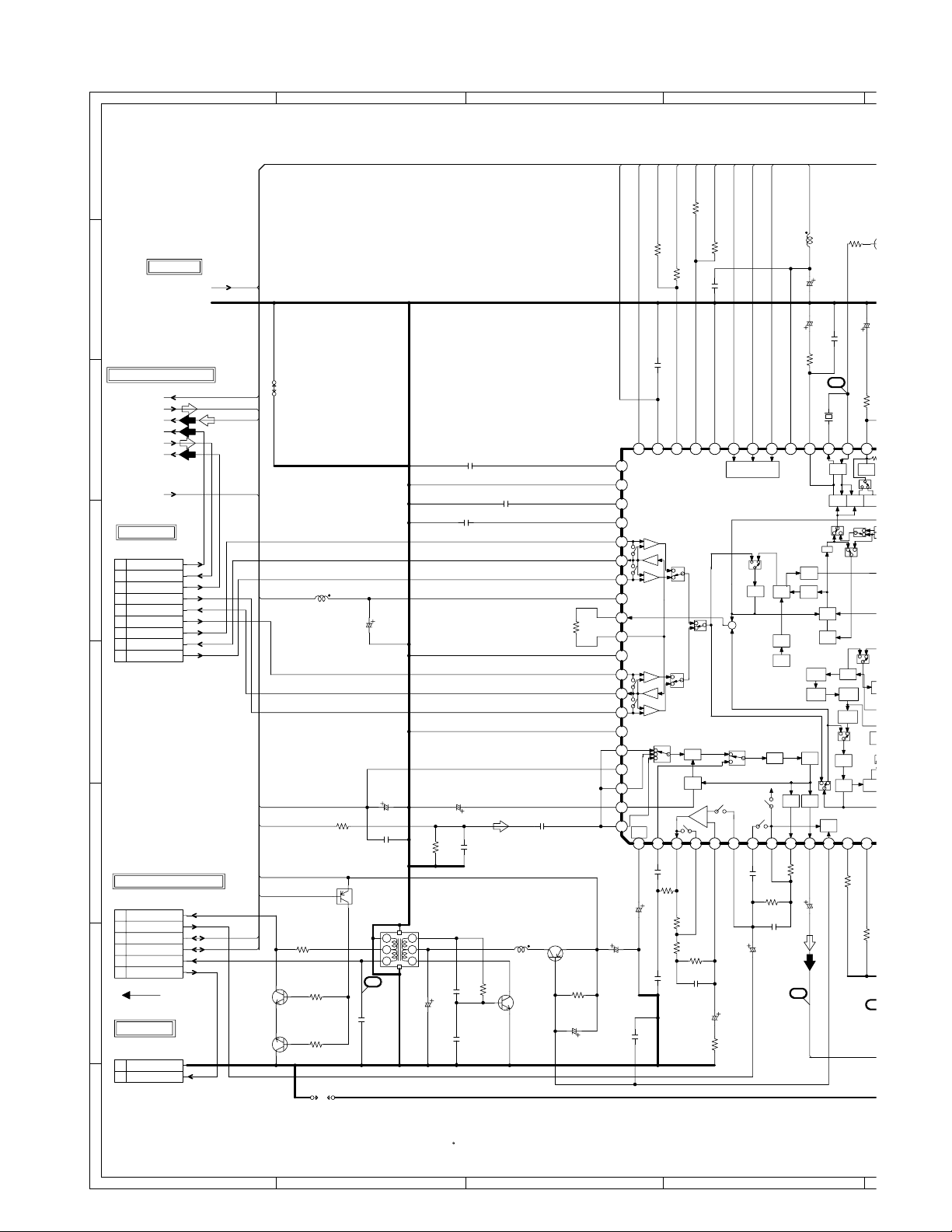
A B C D
K
150V MH7
1.5K
6.8K
R132
C147
8
P
1
3
3
4
C
B
B
-
O
Q
H
Y/C/AUDIO/CCD/HEAD AMP
8
(VCR/DVD
7
FROM/TO HI-FI/DEMODULATOR
TO_NORMAL_A
FROM_NORMAL_A
6
HF_COM
A.VCC
FROM/TO CYL
CP101
TOC-C09X-A1
HF1 (R)
9
5
8
7
6
5
4
EP/LP-CH1 (R)
3
2
EP/LP-CH2 (L)
1
HF_COM
HF2 (L)
SP-CH1 (R)
SP_COM
SP-CH2 (L)
EP/LP COM
4
3
FROM/TO HEAD AUDIO CONTROL
CP102
IMSA-9604S-06Z14
AUDIO REC
6
AUDIO PB
5
CTL+
4
CTL-
3
AE HEAD(+)
2
AE HEAD(-)
1
CD102
FFC
2
2H061504
TO FE HEAD
CP103
B2013H02-2P
FE HEAD(GND)
2
FE HEAD(HOT)
1
FROM/TO POWER
P.CON+5V
FSC
HF1
HF2
GND
GND
HOT
CTL+
CTL-
W845
P.CON+5V
A.VCC
TO_NORMAL_A
P.CON+5V
V.REC_ST-H
AUDIO PB SW
0
KTC3875S_Y_RTK
0.7
0
KTC3875S_Y_RTK
0
0.7
0
L107
22uH
0305
R101
560
Q101
R102
10K
AUDIO PB SW
Q102
R103
10K
S801X S801Y
COMP
ENV.DET
H.AMP_SW
R136
C154
OUT
COMP
2.1
2.9
1.6
1.8
1.9
1.8
5.0
1.8
1K
1.6
1.8
1.8
1.8
2.3
4.9
ENV
DET
KILL
616263646566676869
DET
0
HA
GND
CHROMA
DET
ACC
DET
P
R
P
HA VCC
70717273747576777879
HA
0
PRE GND
P
R
P
0
A-GND
1
2
3
A-VCC
C163
476.3V MH7
C166
0.068 B
C165
0.047 F
C169
0.047 F
R142
2.3
C103
R105
226.3V MH7
C129
1K
1B
5.2
SW
0
Q103
KRA103SRTK
5.3
6
5
20
C101_1
0.022100V MMTS
R106
COIL,BIAS OSC
L101
1626009
1
2
34
C104
2206.3V YK
C105
226.3V MH7
680
C106
C107
C108
C109
0.1 B
0.01 B
R107
0.01 B
3.3K
0
L102
100uH
0305
0
BIAS OSC
0
KTC3203_Y
Y/C/AUDIO/CCD/HEAD AMP IC
BIAS CTL
Q105
KTA1266
0
5.2
Q104
0.015 B
IC101
LA71206M-MPB
5.2
R108
22K
C110
4716V MH7
2.3
C112
22010V MH7
Vref
2.3V
1 101112132 3 4
C116
R109
3310V MH7
C115
C117
0.1 B
C114
0
AUDIO_MUTE-H
R138
22K
R137
12K 1/4W
0.1 B
AUDIO
C-ROT
MUTE
RF-SW
HA SW
H
L
H
L
ALC
ALC
DET
SP,LP
0.1 F
1K
8.2K
R110
8.2K
R111
R112
330K
C118
0.01 B
0.01 B
H.SW
Y/C_CS
C.ROTARY
Y/C_CLK
Y/C_DATA
P.CON+5V
22K
22uH 0305
4716V YK
150V YK
C145
8.2K
17
X101 3.579545MHz
100DT3R528
4.8
4.12.14.8 4.8 0 5.2 0 5.2 5.2 5.2 4.9 3.2
VX01
REC
APC
P
R
BGA
ACC
AMP
PPPR
ACC
DET
R
DETAIL
CLAMP
ENH
NL
EMPHA
EMPHA
R-EQ
TEST
REC
AMP
FM-EQ
FM
R
P
AGC
PHASE
AUTO
BIAS
fo-ADJ
R116
4.750V YK
FROM_NORMAL_A
R129
3.9
1.8K
C146
0.022 B
R131
4849550515253545556575859660
320FH
VCO
R
P
RE
PB
AFC
APC
BEFORE
AFTER
R
P
R
P
Y
NL
FM
MOD
NORMAL
D
PB
FM E
V
PHASE
EQ
EQ
Q-ADJ
1.11.14.80.82.32.3
15K
R117
1
L106_1
C152
C156
R139
12K
0.1 F
C151
R133
SERAIL
DECODER
PR
C-LPF
PB,EE
REC:LP<EP
PB:EP
7
0
C121
VREF
0.0027 B
R114
C122
Main
CONV
4.21M
BPF
Sub
CONV
LPF
8809
20K
C-VCC
R115
3.58M
BPF2
B-UP
AMP
LINE
REC
MUTE
AMP
820
C123
C-GND
IN
+
R
P
PB,EE
EQ
AMP
2.32.32.32.32.32.3
0.0012 B
150V MH7
C120
19
1016V MH7
C119
220
R113
1
NOTE:THIS SCHEMATIC DIAGRAM IS THE LATEST AT THE TIME
OF PRINTING AND SUBJECT TO CHANGE WITHOUT NOTICE
NOTE:THE DC VOLTAGE EACH PART WAS
MEASURED WITH THE DIGITAL TESTER
DURING PLAYBACK.
A B C D
2-3
Page 69

EF GH
C146
R131
R117
15K
3
P
P SCHEMATIC DIAGRAM
PCB)
The Parts Number,value and rated voltage etc. in the Schematic Diagram are for references only.
Note :
When replacing the parts,refer to the Parts List.
8
PB
N.L.
R
150V MH7
ALWAYS
5V
Y-GND
PB-C
DE-EM
R
MAIN
P.CON+5V
L105_1
100uH
0305
C155
1B
FROM/TO AUDIO/VIDEO
DVD_V_OUT[DAC_D]
FSC
C144
0.01 B
C142
4716V MH7
C143
0.1 F
R127
680K
4FscVDD
DRIVER
CCD
VIDEO
AGC
1/2
FBC
R
Y/C
P
MIX
R
P
QV/QH
SUB
LPF
SYNC
V.SYNC
R
P
MAIN
EMPHA
FIL
2.602.01.41.1
NC
AUTO-BIAS
CLAMP
SEP
SEP
4.7K
DET
PLL
CLAMP
S
C141
0.01 B
4142434445464748
CLOCK
0
VSS
1.6
OUTTIMMING
OUT
0
VSS
3.2
IN
2.5
VCA
3.2
VCA
3.3
2.6
VCP
2.6
1
2
3
4.1
REG
4V
2.3
BAL
2.3
TC1
2.1
NC
AGC
1.6
TC2
3.6
6DB
KTA1504S_Y_RTK
C133
1F
C134
1F
C135
0.2250V YK
C136
2235V YK
BUFFER
Q107
1.6
02.2
C137
150V MH7
C140
4.750V NA
R123
C139
0.1 F
4.1
5.0
4.4
Y-VCC
3.2
2.1
B
21 22 23 24 25 26 27 28 29 30 31 32 33 34 35 36 37 38 39 40
2.80.22.6
C131
C132
1006.3V MH7
1F
3.6
R120
220
2.2K
R124
82K
4.2
BUFFER
KTA1504S_Y_RTK
0
R121
Q106
R126
1.8K
4FSC
R122
100K
C138
150V YK
TU/REAR_V_IN
FRONT_V_IN
R143
1K
R141
DVD_V_OUT[DAC_D]
1K
16
Y/C_VIDEO_OUT
C.SYNC
DUMMY_V.SYNC
W809
P.CON+5V
1K
FROM/TO TUNER/JACK
FRONT_V_IN
TU/REAR_V_IN
Y/C_VIDEO_OUT
GND
FROM/TO SYSCON
4FSC
Y/C_CLK
Y/C_DATA
Y/C_CS
DUMMY_V.SYNC
V.REC_ST-H
C.ROTARY
AUDIO_MUTE-H
CTLCTL+
H.AMP_SW
COMP
ENV.DET
H.SW
C.SYNC
7
6
5
4
3
BUFFER
Q109
KTC3875S_Y_RTK
4.9
29
3.9
K
3.3
3.3K
R132
150V MH7
C147
0.022 B
C148
1.5K
NC
.2 4.9 4.9 1.2 2.2 0.8
3.23.3
320FH
SLD
B
VCO
R
P
REC
AFC
C
BEFORE
BGA
BGA
A
MAL
AFTER
P
PHASE
Q-ADJ
CNC
AMP
B.D
P
3.58M
BPF1
PB-C
YNR/COMB
R
DEEM
P
Y-LPF
NC1
R
DOUBBLE
FM
LIM
DEM
PB
S-EQ
P
FM EQ
VHS
SOPB
FM
EQ
AGC
FIL
13 14 15 16 17 18 19 20
C172
22P CH
6.8K
C124
150V MH7
C125
1.8K
R119
390PCH
C126
0.1 B
C127
180P CH
2
V.ENV
18
TP101
NC
CAUTION: DIGITAL TRANSISTOR
2-4
PLAYBACK VIDEO SIGNAL
RECORD COLOR SIGNAL
RECORD LUMINANCE SIGNAL
AUDIO SIGNAL(REC)
AUDIO SIGNAL(PB)
PLAYBACK COLOR SIGNAL
PLAYBACK LUMINANCE SIGNAL
PCBB00
VMB282
1
TUNER VIDEO SIGNAL
EF GH
Page 70

A B C D
O
O
56K
2250V KA
R
G
4
8
FROM/TO POWER
DVD_POWER_CTL
VCR_POWER_ON-L
7
FROM/TO DECK
CP3001
TMC-J12P-B2
6
1
2
3
4
5
6
7
8
9
10
11
12
5
BOT SENSOR
4
Q3008
ST-304L
3
2
CAUTION: DIGITAL TRANSISTOR
1
AT+12.6_V
P.CON+5V
AT+5V[M-CON]
POWER_FAIL
AT+5.2V
GND
MOTOR_GND
CAP FG
CAP VCO
VCC
CAP.M/F/R
I LIMIT
MOTOR GND
GND
LD/CY VCO
CAP CTL
LDM CTL
CYL FG/PG
CYL CTL
5.2
0
270K
R3004
FROM/TO MPEG/MICON
DVD_RESET
TX
RX
FROM/TO AUDIO/VIDEO
SYS_MUTE
R3035
270
R3016
TAB SW
SW3001
LSA-1144EAU
10K1/4W
C3033_1
33035V YK
W906
R3003
5.2
EOT SENSOR
LTE-3271T-012A-O
0
R3026
Q3006
ST-304L
270K
D3001
CAUTION: DIGITAL TRANSISTOR
3.3K
C3040
1F
C3006
(LED_GND)
R3011
AT+12.6_V
CONTROL_IN
CYL_FG/PG
CYL_DRIVE
C3005
0.001 B
47K
TAB_SW
CAP_FG
AT+12.6_V
P.CON+5V
CAP_F/R
CAP_LIMIT
LDM_CTL
AT+5.2V
0.001 B
EOT
BOT
AT+5.2V
AT+5V[M-CON]
AT+5.2V
LDM_CTL
CAP_F/R
CONTROL_IN
CYL_DRIVE
CYL_FG/PG
C3007 0.1 B
AT+5V[M-CON]
P.CON+5V
AT+5.2V
CAP_LIMIT
C3008
0.0047 B
R3001
5.6K
R3024
15K
MS_SEN B
Q3004
RPI-352C40N
24
R3008
1K
23
1
0.9 1.3
VCR SYSCON SCHEMATIC DIA
C3020
0.022 B
R3057
22K
TU_A_MUTE-H
TV/VCR
POWER_MUTE-L
SYS_MUTE
AV_SW1
W835
Y/C_CS
RF_CH_SW
AUDIO_MUTE-H
V.REC_ST-H
C.ROTARY
H.AMP_SW
COMP
R3032
10K
R3031
1M
21
H.SW
HIFI_H.SW
C3004 0.022 B
DUMMY_V.SYNC
C.SYNC
CTL+
R3007
CTL-
MS_SEN-B
MS_SEN A
Q3005
RPI-352C40N
5.15.1
0.9
4
33K
R3083
NOTE:THE DC VOLTAGE EACH PART WAS
R3014 56K
R3017
560
6.8K
0.001 B
R3020
C3010
560
5.1
23
1
4
1.30.4
33K
R3050
100 1/4W
R3087
MEASURED WITH THE DIGITAL TESTER
DURING PLAYBACK.
C3053
R3012
56K
MS_SEN-A
REEL SENS
R3033
0.1 B
NC
NC
NC
2.4
2.5
R3002
1.2
2
34
Q3002 RPI-303
5.2
MD0
10K
0.1 B
C3009
NC
00
3.3
5.0
8586878889
0
5.0
CAP LIMIT
5.1
SYS MUTE
0
FL CLK/VSC CLK
0
FL DATA/VSC DATA
90919293949596979899
5.0
AV SW2
5.0
AV SW1
0.1
Y/C CS
5.1
RF CH SW
0
AUDIO MUTE-H
0
V.REC ST-H
LDM_CTL
0
CAP FWD-L
C.ROTARY
0
H.AMP SW
100
0
COMP
2.7
CAP FULL
0
CYL SPEED UP
3.0
D FG/PG
2.5
VIDEO H.SW
2.5
HIFI H.SW
2.7
DRUM PWM
2.7
CAP PWM
0
DUMMY_V.SYNC
0
VSS (GND)
110 101102103104105106107108109112 111
0.4
5.1
SVSS (GND)
110
C3013
226.3V KA
C3052
REEL-T
47K
120
1/4W
R3006
2.4
1
0
C3025
18P CH
X3001
C3024
18P CH
10MHz
100BT01004
23
R3034
1M
5.1 3.4 2.5 4.9
FL CS/VSC SW
CTL REF
C3016
MD0
CTL(+)
476.3V KA
226.3V KA
REEL-S
VCL
CTL(-)
C3015
820P CH
R3019
27
0 0 5.1 1.4 1.5 0
OSC2
85
86
87
C SYNC
111
VCC (BACK UP)
112
CTL BIAS
67
R3022
C3018
C3019
R3027
C3027
47K
0
2
34
R3062 1K
OSC1
/RESET
VSS (GND)
TUNER L
VCR_H
POWER MUTE-L
CTL SMT(I)
CTL AMP(O)
CTL FB
25
150K
22
150P CH
0.1 B
15K
C3041 0.0015 B
0.1 F
C3029
1.2
1
REEL SENS
Q3001 RPI-303
05.2
RESET
C3050 0.01 B
R3056
C3047
15P CH
X1
CAP FG
9
CAP_FG
KA
476.3V
X3002 32.768KHz
X2
SVCC (P.CON5V)
1K
C3001
C3046
15P CH
R3037 47K
100DA32R01
FWE
AFC PC
11 12 132 3 4 5
R3025
470
L3003
12uH
C3044
12P CH
1B
C3022
NOTE:THIS
FWE
SEG_10
NC
727374757677787988081828384
SEG10
SYSC
AFC OSC
1.52.02.05.12.32.52.60.12.502.500
R3030
C3032
470P CH
OF P
JUST CLOCK
AFC LPF
0.
A B C D
2-5
Page 71

The Parts Number,value and rated voltage etc. in the Schematic Diagram are for references only.
SEG10
Note :
When replacing the parts,refer to the Parts List.
EF GH
GRAM
SEG_8
SEG_7
SEG_9
SEG_10
NC
4.9 0 0 4.8 4.8
SYSCON/TIMER/SERVO
13 14 15 16 17 18 19 20 21 22 23 24 25 26 27 28
R3030
C3032
:THIS SCHEMATIC DIAGRAM IS THE LATEST AT THE TIME
OF PRINTING AND SUBJECT TO CHANGE WITHOUT NOTICE
NCNC
00
SEG9
REC L
JUST CLOCK
IC3001
OEC0132A
AFC LPF
V CYNC
C SYNC/H SYNC
5.6K
C3038
1F
2.250V KA
SW_V_OUT
470P CH
SYSTEM RESET IC
IC3003 PST3231NR
NC
00
NC NC
123
5.0 5.0 0
0.4750V
C3045
SEG_6TXSEG_5
4.8
4.8 0 4.8 4.8
SEG6
SEG8
SEG7
VSC H
CV OUT
OVCC
CV IN2
CV IN1
0.1 F
C3065
470K
R3043
AT+5V[M-CON]
VIDEO_OUT
NC
45
GNDINOUT
KA
(VCR/DVD PCB)
R3028 47K
SCL
SDA
SEG_3
SEG_4
W839
JG3001
W840
0 4.9 5.0 0
SEG5
SEG4
IIC SDA
IIC CLK
4G/TIME SHIFT LED
AVSS (GND)
V ENV
ENV.DET
F
0.1
C3014
C3023
SEG3
5G/CS/BS LED
3G/TV/VCR LED
2G/DUB/REC LED
1G/VCR/T-REC_LED
DVD_POWER_CTL
POWER ON-H
VIDEO_MUTE-H
POWER FAIL
AVCC (BACK UP)
AFT S.CURVE
EOT-H
BOT-H
BOT
EOT
AT+5V[M-CON]
2206.3V YK
SI1/RX
56
55
54
31
30
29
OVSS(GND)
RESET
R3049
47K
D3009
1SS133
SO1/TX
VCC (BACK UP)
SEG1
Y/C DATA
ST SELECT
KEY-A
KEY-B
4FSCIN/2FSCIN
4FSCOUT/2FSCOUT
NC
1F
C3017
4FSC
18K
R3051
1016V KA
C3021
EF GH
2-6
SEG_2
R3044 3.3K
C3061
0.1 F
57585960616263646566676869707172
SEG2
VSS (GND)
Y/C CLK
VCR LED
DVD LED
DVD RESET
REM IN
REEL T
REEL S
POWER ON-L
TAB SW
SERVICE NC
HiFi ENV
MS SEN-B
MS SEN-A
1.31.3002.602.5002.65.12.63.100.41.5
D3007
1SS133
R3010
MS_SEN-B
MS_SEN-A
RX DRIVE
Q3003
KRA103SRTK
W838
0.0015 B
C3034
1K
R3063
R3053
SW_V_OUT
5.2
0
5.3
4.7K
R3009
W837
R3055 22K
R3038 4.7K
1F
R3015
100P CH
C3049
470K
SDA
5.04.9
5678
SDA
VSS
0
0
C3036
0.1 F
SERVICE
TP3001
47K
R30453.3K
5.1
0
4.8
5.0
5.0
5.0
51 52 53 54 55 56
5.0
5.0
5.0
0.3
5.1
0
3.3
4.7
5.0
NC
0
0
0
0.1
5.0
5.1
0
0
2.5
3.7
0
5.2
5.2
29 30 31 32 33 34 35 36 37 38 39 40 41 42 43 44 45 46 47 48 49 50
10K
C3031
4.7K
R3029
3.4
RX
RX DRIVE
Q3007
KRC103SRTK
SEG_1
Y/C_DATA
Y/C_CLK
5G/CS/BS_LED
4G/VSC_LED
3G/TV/VCR_LED
2G/DUB/REC_LED
1G/VCR/T-REC_LED
VCR_LED
DVD_LED
DVD_POWER_CTL
DVD_RESET
REM_IN
REEL-T
REEL-S
VCR_POWER_ON-L
VIDEO_MUTE-H
AT+5.2V
POWER_FAIL
AT+5V[M-CON]
TAB_SW
AFT-S.CURVE
HIFI_ENV.DET
ST_SELECT
KEY-A
KEY-B
10K
R3046
10K
R3047
AT+5.2V
SCL
AT+5.2V
C3030
1F
5.2
0
VCC
SCL
TEST
EEP ROM
A0
A1
A2
1234
0000
AT+5V[M-CON]
IC3099 S-24C02BDP-1A
RECORD LUMINANCE SIGNAL
RECORD COLOR SIGNAL
PLAYBACK LUMINANCE SIGNAL
PLAYBACK COLOR SIGNAL
TX
MD0
RESET
FWE
H.SW
TP3002 H.SW
NC
FROM/TO Y/C/AUDIO/CCD/H.AMP
DUMMY_V.SYNC
C.SYNC
V.REC_ST-H
C.ROTARY
AUDIO_MUTE-H
CTLCTL+
H.AMP_SW
COMP
ENV.DET
H.SW
Y/C_CS
Y/C_DATA
Y/C_CLK
4FSC
FROM/TO TUNER/JACK
RF_CH_SW
SW_V_OUT
AV_SW1
SCL
SDA
AFT-S.CURVE
TV/VCR
VIDEO_OUT
TU_A_MUTE-H
POWER_MUTE-L
VIDEO_MUTE-H
FROM/TO HI-FI/DEMODULATOR
V.REC_ST-H
HIFI_ENV.DET
HIFI_H.SW
AUDIO_MUTE-H
SCL
SDA
ST_SELECT
FROM/TO OPERATION1/DISPLAY
DVD_LED
VCR_LED
KEY-A
KEY-B
REM_IN
1G/VCR/T-REC_LED
2G/DUB/REC_LED
3G/TV/VCR_LED
4G/VSC_LED
5G/CS/BS_LED
SEG_1
SEG_2
SEG_3
SEG_4
SEG_5
SEG_6
SEG_7
SEG_8
SEG_9
SEG_10
JG3006 JG3008JG3007JG3005JG3004JG3003JG3002
PCBB00
VMB282
8
7
6
5
4
3
2
1
Page 72

A B C D
A
4
5
27K
G
8
7
6
5
TU301
115-V-H015AR
19220
A.IN
CH
+B
CONTROL
V.IN
NC
NC
NC
CLOCK
DATA
AFT
A.OUT
SIF OUT
TU 32V
NC
V.OUT
21
1K
Q301
33K
R304
10K
0
C318
1016V
R302
C313
1016V KA
R305
00
RF_CONV_A_OUT
KA
RF_CH_SW
P.CON+5V
TV/VCR
1K1/4W
SCL
SDA
AFT-S.CURVE
+32V
TU_V_OUT
C8013
1050V YK
P.CON+12V
VIDEO MUTE SW
Q8003
KRC103SRTK
VIDEO_MUTE-H
R8009
4701/2W
0
3.3
0
C8015
0
3.3
4706.3V YK
BUFFER
Q8004
KTA1266
2.6
E
1234
5
H1EH1H2
L
V
R
R8010
RF MUTE SW
KTC3875S_Y_RTK
R301
C315
1016V
3
4
5
6
C301
NC
8
NC
9
NC
10
11
12
13
NC
14
15
16
NC
17
18
22
KA
L301
22uH 0305
2206.3V YK
C309
0.01 F
W821
C303
0.1 F
TUNER/JACK SCHEMATIC DIA
REAR OUT JACK
J8001
MSP-213V1-432_PBSN
TP8001
VIDEO OUT
75
R8011
100
C8095
0.022 B
R8014
390
KTC3875S_Y_RTK
R8003
C8010
B8001
R8015
390
MUTE SW
Q8005
68
D AUDIO
DRIVER
Q8001
KTA1504S_Y_RTK
R8004
120
0.1 B
D AUDIO
DRIVER
Q8002
KTC3875S_Y_RTK
FCM2012H-102T04
C8094
MUTE SW
Q8006
KTC3875S_Y_RTK
0
0
0
R8016
2.2K
R8005
0
1.5
1.5
5.1
R8006
0
0
10
10
1.7
1.7
0
476.3V KA
R8017
2.2K
DVD AUDIO OUT
MSP-213V1-732_PB
100
R8007
KRA103SRTK
J8007
R8032
470
MUTE SW
Q8007
E
1
23
H1EH1H2
R8054
R8056
470
05
5.0
C8099
470P CH
C8100
470P CH
AUDIO R
FRONT AV JACK
J8005 MSP-281V2-A
E
1
D8002
23
HNC
MTZJ6.8B
C8019
1016V KA
E
VIDEO
H
FRONT AV JACK
J8003 MSP-281V2-B
75
4
C316
0.1 F
1.2
0
0
TU A MUTE SW
Q303
KRC103SRTK
SIF_OUT
TU_A_MUTE-H
TU/REAR_V_IN
TU_V_OUT
R8019
W810
E
1
2
FRONT AV JACK
AUDIO L
1
2
H
J8004 MSP-281V2-B
3
FRONT_A_IN_L
FRONT_A_IN_R
FRONT_V_IN
2
CAUTION: DIGITAL TRANSISTOR
1
CAUTION: DIGITAL TRANSISTOR
NOTE:THIS SCHEMATIC DIAGRAM IS THE LATEST AT THE TIME
OF PRINTING AND SUBJECT TO CHANGE WITHOUT NOTICE
CAUTION:
SINCE THESE PARTS M
CRITICAL FOR SAFETY,U
DESCRIBED IN PARTS LI
A B C D
2-7
Page 73

GRAM
4
5
H1EH1
T
_PB
34
2.7K
R8055
R8054
8056
470
5.2
5.0
R8065
2.7K
The Parts Number,value and rated voltage etc. in the Schematic Diagram are for references only.
Note :
When replacing the parts,refer to the Parts List.
EF GH
OS8001 GP1FA553TZ
35
470
470
R8067
L8002
100uH
(VCR/DVD PCB)
OPT TRNSFORMER
GND
VCC
INPUT
123
C8096
0.1 F
C8097
100uH
L8007
C8098
0.1 F
Y/C_VIDEO_OUT
DVD_V_OUT[DAC_D]
4716V YK
C8075
Y/C SEPA
J8006
MDC-070V
56
SPDIF
4.750V YK
C8032
32
L8001
0.27uH
12
34
33
L8003
0.27uH
C8031
4.6
4.750V KA
4.8
4.6
0
4.716V KANP
NC NCNC
NC
R8023
R8008
VIDEO SW
1234
BAIAS
2.2
2.2
L
H
S/CVBS COMP
1
2
345678
NCNC
VIDEO OUT SW
SW7001
SK42H0IG9A
R8059
4.7K
IC8005NJM2533V
0
3.8
BUFFER
11.8
VCC
0.8
5678
R8020
1112
131415161718
NC
NCNC
R8078 2.2
D8008
C8057
10K
C8025
1SS133
0.1 F
COMPONENT OUT
J8008
MSP-213V1-652_PBSN
E
1234
33P CH
C8026
33P CH
POWER_MUTE-L
L8004
47uH
2235V YK
C8053
5
H1EH1H2
31
P.CON+5V_DH
AUDIO_OUT_R
AUDIO_OUT_L
AT+5.2V
P.CON+5V
VIDEO_OUT
AV_SW1
SW_V_OUT
P.CON+12V
C8027
33P CH
R8028
2.2
29
R8029
2.2
R8030
2.2
30
FROM/TO Y/C/AUDIO/CCD/H.AMP
FROM/TO HI-FI/DEMODULATOR
C8037
4706.3V YK
C8038
4706.3V YK
C8039
4706.3V YK
TU/REAR_V_IN
FRONT_V_IN
Y/C_VIDEO_OUT
GND
(S801)
FROM/TO SYSCON
SCL
SDA
AV_SW1
TV/VCR
RF_CH_SW
AFT-S.CURVE
POWER_MUTE-L
VIDEO_MUTE-H
TU_A_MUTE-H
VIDEO_OUT
SW_V_OUT
SIF_OUT
FRONT_A_IN_L
FRONT_A_IN_R
AUDIO_OUT_L
AUDIO_OUT_R
RF_CONV_A_OUT
FROM/TO POWER
+32V
AT+5.2V
P.CON+5V
P.CON+12V
P.CON+5V_DH
GND
D8011
D8016
MCL4148
D8012
MCL4148
D8017
MCL4148
D8013
MCL4148
D8018
MCL4148
MCL4148
FROM/TO AUDIO/VIDEO
DVD_Y_VIDEO[DAC_A]
DVD_U[DAC_C]
DVD_V[DAC_B]
SPDIF
DVD_V_OUT[DAC_D]
DVD_A_OUT_R
DVD_A_OUT_L
FROM/TO MPEG/MICON
V_SW
8
7
6
5
4
3
S MARKED BY
ETY,USE ONES
TS LIST ONLY
2-8
2
PLAYBACK VIDEO SIGNAL
TUNER VIDEO SIGNAL
PLAYBACK LUMINANCE SIGNAL
PLAYBACK COLOR SIGNAL
RECORD COLOR SIGNAL
ARE
DANGEREUSES AN POINT DE VUE SECURITE
N’UTILISER QUE CELLS DECRITES
DANS LA NOMENCLATURE DES PIECES
ETANTLES PIECES REPAREES PAR UNATTENTION:
EF GH
RECORD LUMINANCE SIGNAL
AUDIO SIGNAL(REC)
AUDIO SIGNAL(PB)
DIGITAL AUDIO SIGNAL(PB)
PCBB00
VMB282
1
Page 74

A B C D
8
6
8
P
D
OPERATION/DISPLAY S
8
7
6
SEG1 SW
Q664
KRC103SRTK
0
2.0
1.9
1G SW
Q665
KTA1504S_Y_RTK
1.75.2
4.9
820
R675
SEG2 SW
Q663
KRC103SRTK
0
0.4
4.0
R674
180
SEG3 SW
Q662
KRC103SRTK
00.4
2G SW
Q661
4.0
KTA1504S_Y_RTK
5.2 1.7
4.9
R671
R673
180
R672
SEG4 SW
Q660
KRC103SRTK
01.1
4.0
8201/4W
5
180
SEG5 SW
Q658
KRC103SRTK
1.00
3.0
KTA1504S_Y_RTK
5.2 1.7
(VCR/DV
V651 ELF-4M6SDRVGWB
101112131415
9
R670
180
R668
180
3G SW
Q659
SEG6 SW
4.9
Q657
KRC103SRTK
0.40
820
R669
4.0
R6
1
4
3
SEG_1
1G/VCR/T-REC_LED
SEG_2
SEG_3
KEY-A
NC
2G/DUB/REC_LED
R683
560
SEG_4
DVD_LED
0
5.2 5.2
SEG_5
DVD LED SW
KRA103SRTK
W802
3G/TV/VCR_LED
Q666
SEG_6
2
GND
KEY-B
KEY-A
DVD LED
FROM/TO OPERATION1/LED
CAUTION: DIGITAL TRANSISTOR
CAUTION: DIGITAL TRANSISTOR
1
345
1
2
(CP681)
CP651
IMSA-9604S-05Z13
NOTE:THE DC VOLTAGE EACH
MEASURED WITH THE D
DURING PLAYBACK.
A B C D
2-9
Page 75
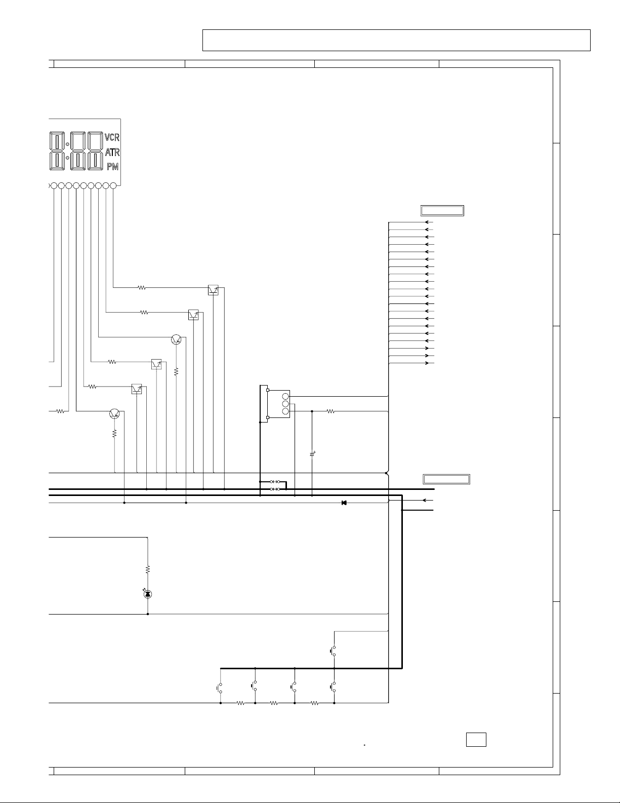
EF GH
A
SCHEMATIC DIAGRAM
VD PCB)
VGWB (ELF-4M6SDRSOWB)
The Parts Number,value and rated voltage etc. in the Schematic Diagram are for references only.
Note :
When replacing the parts,refer to the Parts List.
8
123456789
FROM/TO SYSCON
DVD_LED
VCR_LED
1G/VCR/T-REC_LED
2G/DUB/REC_LED
3G/TV/VCR_LED
4G/VSC_LED
SEG10 SW
Q652
5G SW
Q651
4.9
R661
5G/CS/BS_LED
KRC103SRTK
SEG9 SW
Q653
KRC103SRTK
4.0
5.21.3
820
SEG_9
00.9
4.0
00.4
OS651
PIC-37043LO
SEG_10
Vout
GND
W825
W827
4.9
1
2
0
C652
R651
1001/4W
1006.3V YK
D656
1N4005-EIC
B+
3
5.1
REM_IN
AT+5.2V
AT+5.2V
R662
180
R663
180
KTA1504S_Y_RTK
SEG8 SW
Q655
180
KRC103SRTK
5.2
820
R664
4G/VSC_LED
SEG7 SW
Q656
0
SEG_7
KRC103SRTK
3.5 0
0
03.1
SEG_8
R665
R666
180
4G SW
Q654
K
R667
KTA1504S_Y_RTK
180
1.7
4.9
5G/CS/BS_LED
SEG_1
SEG_2
SEG_3
SEG_4
SEG_5
SEG_6
SEG_7
SEG_8
SEG_9
SEG_10
REM_IN
KEY-B
KEY-A
FROM/TO POWER
MOTOR_GND
AT+5.2V
GND
7
6
5
4
3
R653
D651
VCR_LED
VCR_LED
330
LTL-1CHGT-002A
AT+5.2V
KEY-A
2
SW655
CH DOWN
EVQ21505R
SW652
POWER
SW651
EVQ21505R
VCR EJECT
R657
2.7K
CH PART WAS
HE DIGITAL TESTER
.
NOTE:THIS SCHEMATIC DIAGRAM IS THE LATEST AT THE TIME
OF PRINTING AND SUBJECT TO CHANGE WITHOUT NOTICE
EVQ21505R
R658
1.8K
SW653
VCR/DVD(HDD)
EVQ21505R
R659
1.5K
CH UP
SW654
EVQ21505R
KEY-B
PCBB00
VMB282
1
EF GH
2-10
Page 76

A B C D
L701 1
1050V YK
B
G
G
4
O
D
G
1
B
M
HI-FI/DEMODULATOR SCHEMATIC DIA
8
SCL
SDA
0.001 B
C743
0.2250V MH7
C744
0.1 F
R716
3.3K
SIF_OUT
FSC
C736
7
0.1 B
C734
4.750V YK
C737
4.750V YK
C735
R717
2.2M
6
C752
2216V MH7
C758
2216V MH7
4701/4W
MTZJ5.1B
L702_1
22uH 0305
L703
100uH0305
C754
4716V YK
R718
1K
P.CON+5V
AUDIO_OUT_R
5
4
ST_SELECT
AUDIO_OUT_L
P.CON+12V
RF_CONV_A_OUT
TO_NORMAL_A
FROM_NORMAL_A
A.VCC
R723
D702
C747
1050V YK
C748
0.1 F
C750
2.250V MH7
R719
330
C755
0.022 B
C746
0.1 F
C749
0.1 F
3
HI-FI/AUDIO/HEAD AMP/DEM IC
R720
3.3K
C757
1F
C756
1016V MH7
C751
0.1 F
C759
2235V YK
C760
1F
C701
IC701
AN3663FBP
11.0
0.022 B
3.350V MH7
C702
R721
4.7
0
4.72.32.13.502.2
3.4
DEM_BLK
49
2.7
4.9
2.5
4.2
2.3
0
1.2
4.3
4.3
1.0
2.4
2.3
2.2
0.6
15K
50515253545556575859
6061626364
2.3
R701
MAIN
DEEN
LOG
AMP
USA
AN3663FBP
SW22 L
R
1
0
4.750V YK
C703
C704
1.5K
R702
1.5K
4.5M
CUE
TRAP
BPFAMDEMOD
SUB
SUB
3.5M
BPF
DET
VCO
LOGIC
FM
DEMOD
SUB DEEN
AMP
AMP
RFC
DET
MIX
2 3
2.3 0 2.2 2.4 2.1
C705
4.750V MH7
OUTPUT SW
4
4.750V YK
C706
15K
R722
LR
4.750V MH7
MATRIX
AMP
R
5
C707
LOGIC
95HMz
BPF
COMP
SW17
L
INPUT_SW(R)
VREF1
6
C708
0.1 B
MUTE VC
CTL
MUTE
SW19
R
MUTE
R
INPUT_SW(L)
78
1016V MH7
C709
4142434445464748
A
LO
SW21
FRO
SW
R
L
NORMAL
L
L
FRO
SW2
0.5
C711
1050V YK
C763
C762
680P CH
R703
2
1
NOTE:THE DC VOLTAGE EACH PART WAS
MEASURED WITH THE DIGITAL TESTER
DURING PLAYBACK.
680P CH
10K
10K
R704
DVD_A_OUT_R
DVD_A_OUT_L
NOTE:THIS SCHEMATIC DIA
OF PRINTING AND SU
A B C D
2-11
Page 77

The Parts Number,value and rated voltage etc. in the Schematic Diagram are for references only.
1050V YK
Note :
When replacing the parts,refer to the Parts List.
EF GH
IAGRAM
P.CON+5V
0305
22uH
L701_1
C739
C738
0.01 F
R714
NC
4.90
TE VCO-F0
ADJ
L
LOGIC
PNR RCH
SW21
FROM 1PIN
E
SW18
R
L
MIX
NORMAL
SW16
L
L
BS
FROM 3PIN
SW2
PNR LCH
_SW(L)
)
8
0 0 0 2.0 2.2 0 0 2.4
0.5
1.60
0
ZZ-PROM
S/N
SW NOISE
SW9
AUDIO
LIMIT
BS
PC PB LPF
HIFI
RCH BPF
FM UM
LCH BPF
MIX
HIFI
PC
PB LPF
AUDIO
LIMIT
SW4
SW NOISE
S/N
MIX
REC LPF
LCH VCO
9
10 11 12 13
NC NC
(VCR/DVD PCB)
AUDIO_MUTE-H
4716V YK
1016V MH7
C741
3325V YK
HPF
DET
LINER
SW
HOLD
TIMING
CURR
AMP
1016V MH7
C742
2.40.7
333435363738394041
2.4
2.1
1.8
RECPB
+
-
-
SW11
SW15
1.8
1.8
2.5
0
4.9
0.6
HA1HA2
0
0.7
0
0
H
2.4
L
2.4
0.7
17 18 19 20 21 22 23 24 25 26 27 28 29 30 31 32
27K
0
SW10
SW14
SW13
C740
2.4
SW12
RCH
VCO
REC LPF
NOISE
DET
AGC
14 15 16
C730 0.015 B
C731
0.22 B
D701
1SS133
C732 0.01 F
C729 0.01 B
C722
0.1 B
C723
0.01 F
C724
0.01 F
C725 0.1 B
C726 0.015 B
C727 1016V MH7
C728 1050V YK
HIFI ENV.
TP701
V.REC_ST-H
HIFI_ENV.DET
28
NC
HIFI_H.SW
FROM/TO TUNER/JACK
FRONT_A_IN_R
FRONT_A_IN_L
SIF_OUT
RF_CONV_A_OUT
AUDIO_OUT_L
AUDIO_OUT_R
FRPM/TO AUDIO/VIDEO
DVD_A_OUT_L
DVD_A_OUT_R
FROM/TO Y/C/AUDIO/CCD/H.AMP
HF2
HF1
HF_COM
FSC
FROM_NORMAL_A
TO_NORMAL_A
A.VCC
FROM/TO POWER
P.CON+5V
P.CON+12V
GND
8
7
6
5
4
FROM/TO SYSCON
1016V MH7
C714
1050V YK
C711
DIAGRAM IS THE LATEST AT THE TIME
D SUBJECT TO CHANGE WITHOUT NOTICE
1050V YK
C713
R708
R707
47K
FRONT_A_IN_R
6.8K
C715
1F
C716
680P CH
C720
1050V YK
C719
R712
R711
47K
FRONT_A_IN_L
3350V YK
6.8K
C721
680P CH
V.REC_ST-H
HIFI_ENV.DET
HIFI_H.SW
AUDIO_MUTE-H
SCL
SDA
ST_SELECT
AUDIO SIGNAL(REC)
AUDIO SIGNAL(PB)
PCBB00
VMB282
3
2
1
EF GH
2-12
Page 78

A B C D
5
A
C501
R
D
M
8
7
6
5
4
3
W5T_20*10*10A
BLADE
WIDE
AC120V_60HZ
CD501_4
0R415907
L502
WHITE
BLACK
S502
S501
FH501
EYF-52BC
C525
F501
51MS025L
2.5A 125V
R516
680P2KV RR
R502
D
S
FH502
EYF-52BC
0.22 1W
G
0.5
0.1
SWITCHING
STP5NC50FP
0.82 1W
Q501
R501
C502
W806
+-10%
3.3M 1/2W
12
0.1275V ECQUL
34
0R4A223F20
D510
100
L501
MTZJ27B
HS501
763WAA0186
NC
R508
POWER SCHE
(VCR/DV
D506
RM11C-EIC
D503
RM11C-EIC
R525
C527
10K
0.0082 B
D524
R524
C515
D509
C528_1
0.01500V B
SARS01
1SS133
100
10016V MHE
D530
139.3
NC
142.0
10ELS6N
T501
81260074
8
7
0
6
4
3
2
PHOTO COUPLER
IC503
PS2561L1-1-V(W)
12.5
0.3
C516
0.0047250V KX
34
NC
NC
10
11
0
12
0
13
14
15
5.1
1
4.1
2
0.022 B
R519
C524
1K
D536
MCL4148
D535
1SS133
150
R542
R518
150
D534
1SS133
VOLTAGE CTL
IC501 KIA431
R512
100200V YXF
C511_2
C529
R503
0.1275V ECQUL
1.5M 1/2W
D502
RM11C-EIC
D505
RM11C-EIC
W823
R506
1M1/2W
38
39
R537
220
R504
PROTECT CONTROL
Q502
0.5
KTC3203_Y
0.3
0
D504
1SS133
R538
220
5601/2W
C508
0.0082 B
C509
0.018 M
R507
10K
68K 1W
C513
220P2KV RR
B501
W4BRH3.5X6X1.0X2
D531
MTZJ9.1B
D515
D537
MCL4148
D522
10ELS6N
D507
RGP15J
C531
560P500V B
C519_1
21DQ09N
R528
220010V MHE
R529
2
2.5A 125V
CAUTION:FOR CONTINUED PROTECTION AGAINST FIRE HAZARD,
REPLACE ONLY WITH THE SAME TYPE FUSE
ATTENTION:POUR UNE PROTECTION CONTINUE LES RISQUES D’INCEIE
N’UTOLISER QUE DES FUSIBLE DE MEME TYPE
1
CRITICAL FOR SAFETY,USE ONES
DESCRIBED IN PARTS LIST ONLY
A B C D
ARESINCE THESE PARTS MARKED BYCAUTION:
2.5A 125V(F501).
2.5A 125V(F501).
DANGEREUSES AN POINT DE VUE SECURITE
N’UTILISER QUE CELLS DECRITES
DANS LA NOMENCLATURE DES PIECES
ETANTLES PIECES REPAREES PAR UNATTENTION:
PROTECT
Q530
KTC3875S_Y_RTK
4.1
0
0
100K
R510
NOTE:THIS SCHEMATIC DIAG
OF PRINTING AND SUBJ
GNDOUT IN
02.54.1
2-13
123
PR
Q
2S
Page 79

EF GH
EMATIC DIAGRAM
VD PCB)
07
15J
31
0P B
C501
220016V MHE
3.3V OUT
Q511
KTA1241_Y
3.43.7
3.9K
R528
220010V MHE
1.8 1.8
3.3V CTL
KTC3875S_Y_RTK
2.2K
R529
D511
21DQ09N
D512
21DQ09N
3.2
3.1
1.0 1.0
Q507
D518
1SS133
3.9
KTC3875S_Y_RTK
1/4W
R527
100
C520
820 1/2W
2250V MHE
C522
C510
3.3V CTL
C518_2
560
R517
Q508
1F
22006.3V ZL
D539
R536
R530
2250V MHE
R531
R526
L506
22uH TSL0808
1SS133
D523
33
820
1.2K
R515
MTZJ33B
+-1%
+-1%
6.8K
D538
C506
MCL4148
D513
C521_1
10006.3V
1N4005-EIC
10016V MHE
MHE
L505
22uH
0305
The Parts Number,value and rated voltage etc. in the Schematic Diagram are for references only.
Note :
When replacing the parts,refer to the Parts List.
D525
1N4005-EIC
C533
C505
22016V MHE
9V REG. IC
IC502 KIA78R09API
GNDOUT SWIN
1234
5.2 5.2
5.8
P.CON+5V SW
Q503
KTC3209_Y
M-CON +5V SW
KTA1271_Y
R544
22K
Q504
5.009.011.6
C514_1
33010V MHE
5.2 5.1
0.1
5.1
0
P.CON+12V SW
MHE
22016V
R514
220 1/2W
4.4
R523
6.8K
M-CON POWER SW
Q506
KRC103SRTK
KTC3203_Y
Q510
R535
22K
R533
R534
FROM/TO Y/C/AUDIO/CCD/H.AMP
P.CON+5V
GND
FROM/TO SYSCON
AT+5.2V
DVD_POWER_CTL
VCR_POWER_ON-L
POWER_FAIL
AT+5V[M-CON]
AT+12.6_V
AT+12.6_V
12.4
12.8
220 1/4W
22K
C534
12.2
MTZJ13B
C517
1F
D514
19.1
Q505
KTC3203_Y
P.CON5V SW
R513
390
1/4W
4706.3V MHE
R509
5.9
0
100
P.ON SW
Q509
KRC103SRTK
0
5.2
5.1
P.CON+12V
VCR_POWER_ON-L
MOTOR_GND
W903
W850
DVD_POWER_CTL
P.CON+9V
P.CON+5V_DH
W856
P.CON+3.3V
AT+5.2V
P.CON+5V
AT+5V[M-CON]
POWER_FAIL
GND
GND
GND
+32V
P.CON+5V
GND
MOTOR_GND
FROM/TO TUNER/JACK
P.CON+5V_DH
+32V
AT+5.2V
P.CON+5V
P.CON+12V
GND
FROM/TO OPERATION/DISPLAY
AT+5.2V
GND
MOTOR_GND
FROM/TO HI-FI/DEMODULATOR
P.CON+5V
P.CON+12V
GND
FROM/TO MPEG/MICON
P.CON+5V_DH
P.CON+3.3V
GND
FROM/TOMEMORY
P.CON+3.3V
FROM/TO DSP
P.CON+3.3V
P.CON+9V
GND
FROM/TOMOTOR DRV
P.CON+3.3V
P.CON+9V
GND
MOTOR_GND
FROM/TO READ CHANNEL
P.CON+3.3V
GND
FROM/TO AUDIO/VIDEO
P.CON+5V_DH
P.CON+3.3V
P.CON+12V
AT+5.2V
GND
8
7
6
5
4
3
470
R540
3.3
0
PROTECT
Q531
2SA1037AK
IAGRAM IS THE LATEST AT THE TIME
SUBJECT TO CHANGE WITHOUT NOTICE
100K
R543
3.3
C504_1
2206.3V
R541
YK
D532
MTZJ3.0B
EF GH
2-14
22K1/4W
R521
R520
R522
390
3.3K +-1%
3.3K +-1%
NOTE:THE DC VOLTAGE EACH PART WAS
MEASURED WITH THE DIGITAL TESTER
DURING PLAYBACK.
CAUTION: DIGITAL TRANSISTOR
PCBB00
VMB282
2
1
Page 80

A B C D
4
P
GNDP
GNDADC
9
8
7
FROM/TO AUDIO/VIDEO
6
5
4
3
FROM/TO MOTOR DRV
2
FROM/TO READ CHANNEL
1
FROM/TO TUNER/JACK
DAC_C_VIDEO
DAC_B_VIDEO
DAC_D_VIDEO
DAC_A_VIDEO
CD/DVD
SPDIF-DVD
ASDATA0
ABCLK
ALRCLK
AMCLK
MDI
MC
ML
D_GND
FROM/TO DSP
AMCLK
AVD7
AVD6
AVD5
AVD4
AVD3
AVD2
AVD1
AVD0
DREQ
DACK
DERR
DBGN
DCLK
C2F
LRCK
BCK
CD_DATA
LSI_RST
RDY
INT_DEC
WRQ
TE_BIAS
HD0
HD1
HD2
HD3
HD4
HD5
HD6
HD7
HA0
HA1
HA2
HA3
HA4
HA5
HA6
HA7
HA8
HA9
HA10
HA11
HA12
RD
WR
CS_DVD
SPD_FG
EMPH
OPEN
DMUTE
OPN_SW
CLS_SW
LSW
CLOSE
P.CON+A5V
GUP
P.CON+A5V
V_SW
GND
JG4009
R4058
C4071
0.01 B
0.1 F
4.7K
W900
C4001
W858
JG4011JG4012
JG4008 JG4007
JG4010
P.CON+A5V
R4001
4.7K
R4002
4.7K
R4056
4.7K
R4055
FCM2012H-102T04
C4006
C4076
100P CH
C4005
0.1 F
LSI_RST
TE_BIAS
FP_SEL
FP_CLK
AVD7
AVD6
AVD5
AVD4
AVD3
AVD2
AVD1
AVD0
DREQ
DACK
DERR
DBGN
DCLK
OPEN
DMUTE
OPN_SW
CLS_SW
LSW
RDY
CLOSE
R4013 4.7K
GUP
C2F
LRCK
BCK
CD_DATA
INT_DEC
IRIRQ
WRQ
MDI
MC
SPD_FG
FP_DOUT
FP_DIN
GND
4.7K
B4001
4716V YK
JG4005
R4004
4.7K
R4006
4.7K
R4007
4.7K
R4052 4.7K
R4044 4.7K
C4004
0.1 F
R4049
SO1
SI1
SO2
SI2
R4008
R4003 4.7K
C4072
0.01 B
R4051
4.7K
C4002
0.1 F
R4009
4.7K
C4077
100P CH
R4012
4.7K
C4003
0.1 F
R4014
4.7K
10K
SCHEMATIC DIAGRAMMPEG/MICON
IC4003
V_IN V_C
12
3.23.2
10016V YK
C4012 0.1 F
DAC_B_VIDEO
DAC_D_VIDEO
DAC_A_VIDEO
3.1
1.0
1.600
Y/R/V
CVBS/C
DACVDD
MEMAD_18
MEMAD_19
VDDA
GNDA
VDDIP
RAMDAT_15
VDDP
RAMDAT_0
MEMDA_0
MEMDA_8
MEMDA_1
VDDP
RAMDAT_5
RAMDAT_11
1.9
3.2
1.7
C4018
0.1 F
SD_D11
SD_D4
1.
C4015 0.1 F
0.1 F
C4021
16168169170171172173174175176177178179180181182183184185186187188189190191192193194195196197198199200201202203204205206207208
DACGNDD
CVBS/G/Y
RAMDAT_4
RAMDAT_12
0
1.9
SD_D12
0000
1234
NC NC NC GND
EEPROM
S-24C04BFJ-TB
VCC WP SCL SDA
IC4002
R4016
4.7K
0.1 F
C4007
4.7K
R4017
SI1
SO1
ML
4.7K
V_SW
R4059
SI2
1K
C4069
C4085
SO2
3.200
3.2
4.6
3.2
3.2
2.6
2.9
1.6
1.6
1.6
1.6
1.6
1.6
1.6
3.2
1.6
1.6
2.1
3.3
3.3
1.6
3.2
3.3
1.9
3.3
3.2
3.2
3.3
3.2
4.4
2.7
3.3
3.2
3.2
3.2
0.2
3.2
0.1 F
4.5
110111213141516171819 22021222324
0
0
0
0
0
0
0
0
0
0
0
0
0
0
0
0
JTDI
3
4
GPCIO_14
5
GPCIO_13
GPCIO_12
GPCIO_11
GPCIO_10
ATDD_7
ATDD_8
ATDD_6
ATDD_9
ATDD_5
ATDD_10
GNDP
ATDD_4
VDDP
ATDD_11
ATDD_3
ATDD_12
ATDD_2
ATDD_13
ATDD_1
ATDD_14
2526272829
ATDD_0
ATDD_15
ATIOW
VDDC
ATIOR
GNDC
30313233343536373839
ATIORDY
ATINTRQ
GNDP
ATDA_2
VDDP
ATDA_1
ATDA_0
ATCS_1
ATCS_0
40414243444546474849
GPCIO_0
GPCIO_1
GPCIO_2
GPCIO_3
GPCIO_4
GPCIO_5
GPCIO_6
GPCIO_7
VDDIP
GPCIO_8
50
5152
GNDP
53 545556 57 58 59660 61 62 63 64 65 66 67 68 69770 71 72 73 74 75 76 77 78 79880 81 82 83 84 85 86 87 88 89990 91 92 93 9
0.1
0.1
SD_A4
SD_A3
SD_A5
100P CH
R4062
3.2
3.2
3.20003.203.3
JTCK
JTMS
JTDO
ICETD1
1
2
3
206
207
208
50
51
52
53
54
55
RAMADD_2
RAMADD_6
RAMADD_1
RAMADD_7
0.1
0.1
0.1
0.100.1
SD_A2
SD_A6
SD_A1
SD_A7
1.8V
JG4013
FP_RDY
4.7K
ICETMS
ICETDO
VDDP
DUPRD
GPCIO_19
TEST_MODE
GNDP
DUPTD
GNDP
GPCIO_9
VDDP
RAMADD_4
RAMADD_3
RAMADD_5
RAMADD_0
VDDP
0.1
3.2
C4008
0.1 F
SD_A0
R4018
ICETCK
RAMADD_8
0.1
SD_A8
SD_A10
4.7K
3.20003.2
GPCIO_15
GPCIO_17
GPCIO_16
RAMBA_1
GNDP
RAMADD_10
3.200.1
33
R4019
RAMCS0#
R4020 4.7K
GPCIO_21
GPCIO_20
RAMBA_0
RAMADD_9
0.1
0.1
SD_A9
SD_BA0
R40214.7K
C4010
ABCLK
C4070 0.1 F
R4022
1.601.6
AIN
VDDP
VDDP
RAMADD_11
2.903.2
NC
0.1 F
ALRCLK
R4025
100
GNDP
ABCLK
RAMCS_N
RAMRAS_N
NC
R4024 33
RAMRAS#
C4041
10P
CH
100
0
AOUT2
ALRCLK
GNDP
RAMCAS_N
3.103.0
R4026 33
RAMCAS#
3.203.3 3.2
ASDATA0
1.8V
33
R4028
1.90001.6
0
VDDC
AOUT1
AOUT0
VDDP
RAMWE_N
RAMDQM
3.203.1
C4014
R4027 33
RAMDQM
RAMWE#
C4013 0.1 F
NCNC NC NC NC NCNC
GNDC
GPAIO
MPEG/MICON
PCLK
GNDP
0.1 F
R4029 100
RAMCLK
5678
W849
AMCLK
C4084
SPDIF-DVD
0.1 F
R4030
100
3.2
1.60001.201.4
VDDP2
AMCLK
SPDI/F
IC4001
ZR36742
RAMDAT_8
GNDC
RAMDAT_7
0.701.901.6
SD_D8
SD_D7
C4009_1
2
R4031 100
GNDP2
VDDC
1.8
10016V YK
CD/DVD
R4078 3.3K
COSYNC
RAMDAT_9
3.2
1.8
C4017
SD_D9
C4016
B4009
R4035 390+-1%
RSET
DACGNDP
VDDP
RAMDAT_6
1.6
0.1 F
SD_D10
SD_D6
0.1 F
DACGNDB
RAMDAT_10
C4011_1
DAC_C_VIDEO
FCM2012H-102T04
1.0
C/B/U
154
155
156
157 RESET
158
159
102
103
104
105
106
107
GNDP
1.501.9
SD_D5
A B C D
2-15
Page 81

The Parts Number,value and rated voltage etc. in the Schematic Diagram are for references only.
0
C4021
SD
D4
RAMDAT
4
CVBS/G/Y
1.9
1.6
Note :
When replacing the parts,refer to the Parts List.
EF GH
(VCR/DVD PCB)
8
3 PQ070XZ01ZP
REG+1.8V
V_OUT
V_C
V_ADJ GND
6
2345
C4015 0.1 F
0.1 F
001.0
DACGNDD
_18
_19
T_15
T_0
_0
_8
_1
_
RAMDAT_12
293949596979899
_
SD_D12
C4020
NCNCNC
GNDADC
SERADC0
GNDP
RAMDAT_3
1.801.9
SD_D3
R4032
R4033
4716V YK
C4022
0.8
0.9
SERADC1
RAMDAT_13
3.2
2.0
C4024
SD_D13
510 +-1%
10
X4001
4716V YK
3.2
VDDADC
SERADC2
VDDP
RAMDAT_2
1.9
0.1 F
SD_D2
01.21.9
27MHz
1.4
GCLK1
RAMDAT_14
1.3
SD_D14
R4034 1K +-1%
C4026
W808
R4036
1.4
1.6
X0
GCLK
MEMAD_17
MEMAD_16
MEMAD_15
MEMAD_14
MEMAD_13
MEMAD_12
MEMAD_11
MEMAD_10
MEMAD_9
MEMAD_8
MEMAD_7
MEMAD_6
MEMAD_5
MEMAD_4
MEMAD_3
MEMAD_2
MEMAD_1
MEMAD_0
MEMCS0
MEMCS1
MEMDA_15
MEMDA_7
MEMDA_14
MEMDA_6
MEMDA_13
MEMDA_5
MEMDA_12
MEMDA_4
MEMDA_11
MEMDA_3
MEMDA_10
MEMDA_2
GNDP
RAMDAT_1
100
101102 103104
SD_D1
18P CH
1
1M
3.203.2
VDDP
GNDP
VDDP
GNDP
GNDC
VDDC
MEMWR
MEMRD
VDDP
GNDP
MEMCS2
VDDP
GNDP
MEMDA_9
000
3.2
C4027
SD_D15
15715815916016116216316416516616716869
0.1 F
C4028
1.7
SD_D0
0.1 F
105106 107108109110111112113114115116117 118119 120121 122123 124125 126127 128129 130131132133134135136137138139140 141142 143144 145146 147148 149150 151152 153154 155156
1.9
0.2
1.6
3.2
0.7
0
1.2
1.7
1.0
0.8
1.5
2.5
1.3
1.6
1.5
3.2
1.4
0
1.7
1.6
1.3
1.7
2.5
1.6
0
2.5
1.9
3.2
2.6
3.2
2.6
0
3.2
3.2
0.7
1.9
1.3
1.2
0.6
0.7
3.2
0.8
0
1.6
1.6
1.6
1.3
1.2
1.4
1.4
0.9
1.6
C4075
C4029
0.01 B
R4076
10K
C4033
0.1 F
R4060 2.2
R4038 4.7K
C4034 0.1 F
4716V YK
4716V YK
C4035
0.1 F
C4030
L4002
DVD_RESET
2.2uH
C4032
0.1 F
C4031 0.1 F
R4039
4.7K
C4040
0.1 F
C4038
B4002
FCM2012H-102T04
HA18
HA17
HA16
HA15
HA14
HA13
HA12
HA11
HA10
HA9 SO1
HA8
HA7
HA6
HA5
HA4
HA3
HA2
HA1
HA0
C4042
WR
RD
MEMCS0
CS_DVD
HD15
HD7
HD14
HD6
HD13
HD5
HD12
HD4
HD11
HD3
HD10
HD2
HD9
HD1
HD8
HD0
0.1 F
B4004
1.8V
FCM2012H-102T04
B4005
FCM2012H-102T04
B4006
FCM2012H-102T04
B4003
FCM2012H-102T04
JG4006
2206.3V YK
C4046
C4045_1
FROM/TO MEMORY
SD_A4
SD_A3
SD_A5
SD_A2
SD_A6
SD_A1
SD_A7
SD_A0
SD_A8
SD_A10
RAMCS0#
SD_A9
SD_BA0
RAMRAS#
RAMCAS#
RAMWE#
RAMDQM
RAMCLK
SD_D8
SD_D7
SD_D9
SD_D6
SD_D10
SD_D5
SD_D11
SD_D4
SD_D12
SD_D3
SD_D13
SD_D2
SD_D14
SD_D1
SD_D15
SD_D0
HA18
HA17
HA16
HA15
HA14
HA13
HA12
HA11
HA10
HA9
HA8
HA7
HA6
HA5
HA4
HA3
HA2
HA1
HA0
WR
RD
MEMCS0
HD15
HD7
HD14
HD6
HD13
HD5
HD12
HD4
HD11
HD3
HD10
HD2
HD9
HD1
HD8
HD0
476.3V KA
0.1 F
C4036
P.CON+A5V
0.1 F
JG4001
JG4002
JG4003
JG4004
L4001
2.2uH 0305
SI1
NOTE:THE DC VOLTAGE EACH PART WAS
MEASURED WITH THE DIGITAL TESTER
DURING PLAYBACK.
NOTE:THIS SCHEMATIC DIAGRAM IS THE LATEST AT THE TIME
OF PRINTING AND SUBJECT TO CHANGE WITHOUT NOTICE
W895
W866
FROM/TO POWER
GND
P.CON+5V_DH
P.CON+3.3V
FROM/TO SYSCON
DVD_RESET
TX
RX
PCBB00
VMB282
7
6
5
4
3
2
1
2-16
EF GH
Page 82

A B C D
O
C
A
8
7
6
5
4
3
2
FROM/TO MPEG/MICON
MEMCS0
RD
WR
HD8
HD9
HD10
HD11
HD12
HD13
HD14
HD15
HD7
HD6
HD5
HD4
HD3
HD2
HD1
HD0
HA18
HA17
HA16
HA15
HA14
HA13
HA12
HA11
HA10
HA9
HA8
HA7
HA6
HA5
HA4
HA3
HA2
HA1
HA0
SD_A4
SD_A3
SD_A5
SD_A2
SD_A6
SD_A1
SD_A7
SD_A0
SD_A8
SD_A10
SD_A9
SD_BA0
RAMCS0#
RAMRAS#
RAMCLK
RAMCAS#
RAMWE#
RAMDQM
SD_D8
SD_D7
SD_D9
SD_D6
SD_D10
SD_D5
SD_D11
SD_D4
SD_D12
SD_D3
SD_D13
SD_D2
SD_D14
SD_D1
SD_D15
SD_D0
FROM/TO POWER
P.CON+3.3V
S-DRAM
IC4005 MSM56V16160F-8
0
VSS
50
C4048
0.1 F
C4049
0.1 F
C4055
0.01 B
1.1
I/O15
1.1
I/O14
0
VSSQ
1.9
I/O13
1.6
I/O12
3.3
VCCQ
1.3
I/O11
1.9
I/O10
0
VSSQ
1.9
I/O9
40 41 42 43 44 45 46 47 48 49
1.5
I/O8
3.3
VCCQ
0.1
NC
NC
0
3
C4050
DQMU
1.6
CLK
3.3
CKE
0.1
NC
NC
33 34 35 36 37 38 39
0.1
A9
0.1
A8
0.1
A7
30 31 32
0.1
A6
0.1
A5
0.1
A4
0
VSS VCC
26 27 28 29
10016V YK
SD_D15 SD_D0
SD_D14 SD_D1
SD_D13 SD_D2
SD_D12 SD_D3
SD_D11 SD_D4
SD_D10 SD_D5
SD_D9 SD_D6
SD_D8 SD_D7
RAMDQM RAMWE#
RAMCLK RAMCAS#
SD_A9 SD_BA0
SD_A8 SD_A10
SD_A7 SD_A0
SD_A6 SD_A1
SD_A5 SD_A2
SD_A4 SD_A3
B4007
FCM2012H-102T04
B4008
FCM2012H-102T04
I/O0
I/O1
VSSQ
I/O2
I/O3
VCCQ
I/O4
I/O5
VSSQ
I/O6
I/O7
VCCQ
DQML
110111213141516171819 2202122232425
VCC
3
4
5
6789
3.3
WE
CAS
RAS
CS
A11
A10
A0
A1
A2
A3
C4051
3.3
0.1 F
1.4
1.4
0
1.4
1.4
3.3
1.4
1.6
0
0.6
0.6
3.3
3.0
3.1
3.0
3.0
0.1
0.1
0.1
0.1
0.1
0.1
3.3
C4053
0.1 F
C4052
0.1 F
0
C4054
0.1 F
RAMDQM
RAMRAS#
RAMCS0#
MEMORY SCHEM
(VCR/DVD P
C4043
C4063
0.01 B
4716V YK
1
FROM/TO AUDIO/VIDEO
D_GND
A B C D
NOTE:THIS SCHEMATIC DIAGRAM IS THE LATEST AT THE TI
OF PRINTING AND SUBJECT TO CHANGE WITHOUT N
2-17
Page 83

The Parts Number,value and rated voltage etc. in the Schematic Diagram are for references only.
4716V YK
Note :
When replacing the parts,refer to the Parts List.
EF GH
ATIC DIAGRAM
CB)
FLASH 8M
IC4007 SST39VF800A-70-4C-EK
HA16 HA15
HD15 HA12
HD7 HA11
HD14 HA10
HD6 HA9
HD13 HA8
HD5
HD12
HD4 WR
C4062
0.1 F
HD11
HD3
HD10
HD2 HA18
HD9 HA17
HD1 HA7
HD8 HA6
HD0 HA5
RD HA4
MEMCS0 HA2
HA0 HA1
1.2
A16
3.3
NC
0
VSS
0.7
DQ15
1.9
DQ7
1.3
DQ14
1.2
DQ6
0.6
DQ13
0.7
DQ5
40 41 42 43 44 45 46 47 48
0.8
DQ12
1.6
3.3
VDD
1.6
DQ11
1.6
DQ3
1.3
DQ10
1.2
DQ2
1.4
DQ9
1.4
DQ1
0.9
DQ8
30 31 32 33 34 35 36 37 38 39
1.6
DQ0
2.6
DE#
0
VSS
W804
2.6
CE#
2.5 1.6
A0
25 26 27 28 29
1.7
110111213141516171819 22021222324
A15
1.0
A14
0.8
3
A13
1.5
4
A12
2.5
56789
A11
1.3
A10
1.6
A9
1.5
A8
0
NC
NC
0
NC
NC
3.3
WE#DQ4
0
NC
NC
0.1
NC
NC
0.1
NC
NC
0
NC
NC
1.6
A18
0.7
A17
1.4
A7
1.6
A6
1.6
A5
1.3
A4
1.7
A3
2.5
A2
A1
8
7
HA14
HA13
6
5
4
HA3
3
HE TIME
UT NOTICE
NOTE:THE DC VOLTAGE EACH PART WAS
MEASURED WITH THE DIGITAL TESTER
DURING PLAYBACK.
PCBB00
VMB282
2
1
EF GH
2-18
Page 84

A B C D
4
JG2007
0
8
X16MIO
DSP SCHEMATIC DIAGRAM
8
#MOE
#MCASL
DR_D9
DR_D15
DR_D14
DR_D13
DR_D12
001.0 1.0 1.0 1.0 1.0 1.0 1.0 1.7 13.0 3.0 3.0
1.0
1506.3V ZL
C2021
7
C2022
VSS
I/O 15
I/O 14
I/O 13
0.1 B
VCC
1.0 1.0 1.0 1.0 1.0 1.0 1.0 1.0
I/O 0
I/O 1
I/O 2
DR_D11
VSS
I/O 12
I/O 11
VCC
I/O 4
I/O 3
56789
DR_D10
I/O 10
I/O 5
DR_D8
I/O 9
I/O 8
DRAM
IC2002
M11L416256SA-35T
I/O 7
I/O 6
10
0
32353637383944041424344
13 141 15 16 172
#MCASU
CASH
WE
DR_A8
282933031
OE
A8
NC
RAS
23.13.33.33.33.3
NCNC
NC
CASL
00
NC
MD11
MA9
DR_D10
1.4
MD10
MA10
0.2
JG2005
DR_D9
1.4
MD9
MOEB
2.9
#MOE
DR_D8
C2055
MD8
MCASUB
3.0
3.0
#MCASU
#MCASL
#MWE
SPDIF-CD
10P CH
100
R2007
3.301.4
DVSS
DVDD1
HADR7
MCASLB
1.4
HA7
DOUT
HADR8
1.5
HA8
6
C2032
EFLG
131
132
133
134
87
HADR9
1.8
HA9
#MRAS
4P CH
3.300
88
89
90
1.2
HA10
JG2006
FSX
DVDCKIO
DVDD0
DVSS
DVDD2
XIN
LRSY
DVDD1
DVSS
EMPH
HADR10
HADR11
2.4
HA11
16.9
X2
TEST2
HADR12
2.9
HA12
W
1.600
137138139140141142143144145146147148149150151152153154155156157158159160161162163164165166167168169170171172173174175176
3.3
C2F
DR_D0
DR_D1
DR_D2
DR_D3
DR_D4
DR_D5
DR_D6
DR_D7
6
JG2003
R2004 6.8K
C2018
470P CH
R2003
100K
R2006 4.7K
C2019
0.1 B
TE_BIAS
C2020
C2054
JG2001
0.1 F
10P CH
1.7
1.0
0.3
2.0
2.3
1.3
1.7
1.7
1.7
1.6
1.7
1.7
1.6
1.7
3.3
1.7
1.7
1.7
1.7
1.8
1.7
1.5
1.5
1.7
1.7
1.6
1.7
1.5
1.7
1.7
2.5
3.2
3.2
3.2
3.2
2.6
3.2
3.2
1.6
3.3
FROM/TO READ CANNEL
VR
LDON1
LDON2
XHTR
ADRREC
ADPH
ADBH
ADTE
ADFE
RFP
FOST
TOST
TBAL
FBAL
DVD_CD
DEFECTO
RFN
BHC
WO
TEC
FC
BST
SGC
5
4
FROM/TO MOTOR DRV
VR
SLD
SPD
3
TD
FD
SP+
SP-
SLD
SPD
TD
FD
C2002
VR
KFG
ADJV
ADRREC
ADPH
ADBH
ADTE
ADFE
RFP
RFN
BHC
WO
0.1 F
TEC
FOST
TOST
FC
BST
TBAL
FBAL
SGC
SPD_FG
INT_DEC
RDY
LSI_RST
RD
WR
CS_DVD
HD0
C2006
C2015
470P CH
1006.3V YK
0.1 F
C2009
2
C2003 0.1 F
110111213141516171819 22021222324
3
JV
4
RREC
RF_PH
6
RF_BH
TE
FE
0
9
TEST0
EFMINP
0
TEST1
EFMINN
SLCLPFO
SLCLPFI
SLCO1
SLCO2
AVDD1
0
AVSS
BHC
WO
TEC
VREF
TSTD1
TSTD0
FO
2526272829
BST
TBAL
FBAL
SGC
SLDO
30313233343536373839
SPDO
TDO
FDO
DVDD0
0
DVSS
FG
HIRQB
HWAITB
HRESB
HRDB
4041424344
HWRB
HCSB
45 46 47 48 49550
0
JG2002
0.1 F
C2023
0
2.501.7
HFLIO
HDAT2
1.7
1.6
HD1
HD2
TESIO
HDAT3
1.7
HD3
WRQ
XHTR
LDON2
LDON1
DEFECTO
DVD_CD
3.3
3.3
0
RFP0
RFP1
RFP2
RFP3
1
2
175
176
43
44
45
46
HDAT4
1.4
HD4
DEFECTI
DEFECTO
AD1
AD0
DVDD0
DVSS
HDAT0
DVDD1
DVSS
HDAT1
HDAT5
HDAT7
HADR0
HDAR1
HDAT6
51 52 53 545556 57 58 59
0.7
1.6
1.6
3.2
3.2
HD5
HD6
HD7
HA0
HA1
DR_D15
DR_D14
DR_D13
DR_D12
1.503.3
MD15
DR_A4
0.1
MD14
MA5
1.7
DR_A5
1.5
MD13
MA6
1.5
DR_A6
MD12
MA7
1.6
DR_A7
MA8
1.6
DR_A8
DR_D11
1.401.5
NC
0.1
JG2004
DR_D7
DR_D6
DR_D5
DR_D4
DR_D3
DR_D2
DR_D1
DR_D0
0.1 F
C2024
1.4
3.3
1.4
1.4
1.4
1.4
3.303.202.7
NC
MD5
MD6
MD7
MD4
DVSS
DVDD1
MWEB
HADR6
HADR4
HADR5
MRAS1B
60 61 62 63 64 65 66 67 68 69770 71 72 73 74 75 76 77 78 79880 81 82 83 8
1.4
0.2
1.4
3.1
2.6
1.7
#MRAS
HA4
DR_A0
HA5
HA6
#MWE
0.2
HA2
HADR2
0.2
HA3
HADR3
1.4
1.4
MD1
MD2
MD3
DSP
IC2001
LC78663NRW
MA0
MA1
MA2
1.7
1.7
DR_A1
DR_A2
1.4
MD0
MA3
1.7
C2027
DR_A3
0.1 F
C2028
NC
NC
NCNCMA4
3.301.7
0.1 F
1
NOTE:THIS SCHEMATIC DIAGRAM IS THE LATEST AT THE TIME
OF PRINTING AND SUBJECT TO CHANGE WITHOUT NOTICE
NOTE:THE DC VOLTAGE EACH PART WAS
MEASURED WITH THE DIGITAL TESTER
DURING PLAYBACK.
C2F
A B C D
2-19
Page 85

EF GH
2
JG2006
HADR11
V
V
DVDCKIO
(VCR/DVD PCB)
DR_A8
DR_A7
DR_A6
DR_A5
1.7 1.7 1.7 1.7
A8
A7
NC
A0
17 18 19 20 21 22
NC
DR_A0
DR_A1
DR_A4
0
A6
A5
A4
A3
A2
A1
3.31.81.71.72.6
DR_A2
DR_A3
The Parts Number,value and rated voltage etc. in the Schematic Diagram are for references only.
Note :
When replacing the parts,refer to the Parts List.
SP-
SP+
5.6K
5.6K
R2033
R2031
232425262728
VSS
0 2.5 2.6 0.9
GND +IN1 -IN1 OUT1
DUAL OP-AMP
VCC
+IN2 -IN2 OUT2 VCC
5678
C2047
0.001
B
R2034
4.7K
R2036
10K
1234
IC2003BA10358F-E2
8.91.71.71.7
0.1 F
C2049
R2037
4.7K
R2038
KFG
D2001
18K
MCL4148
C2053
0.01 B
8
7
16.9344MHz
X2001
R2011
W860
JG2007
0
9
DVSS
TEST2
X16MIO
VDD0
SS
DD2
N
EFMOUT
RSY
VDD1
VSS
MPH
C2F
HADR12
ROMXA
83 84 85 86 87 88
000
2.9
3.3
HA12
1M
5
1.6
1.601.6
XOUT
VCOC
VRPFR
VPDO
AVSS
AVDD3
JVRVO
JVAIN
JVAO
JVCPC
JVCPI
AVSS
AVDD2
DVDFR
CDFR
FISET
PISET
PCN
LF3
LF2
LF1
FPDO
PPDO
VCOCTL
DVSS
DVDD0
PCK
AVD7
AVD6
AVD5
AVD4
AVD3
AVD2
AVD1
AVD0
AVERRB
AVSCTB
AVDACK
AVACKO
AVREQI
ROMCK
VR
FROM/TO POWER
7
AMCLK
0.1 F
C2036
3.3
133134135136137138
0
2.5
1.2
1.0
1.2
0
2.5
0
0
0.3
0
1.9
0
3.3
0.3
0
1.3
1.3
0.8
1.6
0
0.4
1.3
1.3
1.3
0
2.5
1.6
1.6
1.6
1.6
1.6
101102 103104105106107108109110111112113 114115 116117 118119 120121 122123 124125 126127128129130131132
1.6
100
1.6
1.6
1.6
1.6
3.3
3.3
1.6
2.2
2.0
0
0
89 90 91 92 93 94 95 96 97 98 99
3.3
C2034
0.1 F
C2039
C2037
R2016 10K
R2015
6.8K
C2038 0.01 B
R2017 10K
R2020
R2018
1.2K
1.8K
JG2008
NC
0.1 F
C2041
C2042
0.1 B
0.1 B
0.1 B
JG2009
JG2010
C2044
R2025
R2026
R2029
5.6K
R2028
0.1 B
220
C2045 0.1 F
ADJV
C2043
560P CH
1.2K
680
AVD7
AVD6
AVD5
AVD4
AVD3
AVD2
AVD1
AVD0
DERR
DBGN
DCLK
DACK
DREQ
EMPH
2.5V
B2001
FCM2012H-102T04
A2.5V
R2032
C2046
123
V_IN GND V_C
V_OUT NR
IC2004 PQ1X251M2ZP
C20501FC2051
22K
R2035
22K
0.1 B
0.1 B
C2048
2.5 1.2
REG+2.5V
C2052
1F
3.303.3
45
0.1 F
P.CON+9V
P.CON+3.3V
GND
FROM/TO MPEG/MICON
WRQ
C2F
CD_DATA
BCK
LRCK
AVD7
AVD6
AVD5
AVD4
AVD3
AVD2
AVD1
AVD0
DERR
DBGN
DCLK
DACK
DREQ
EMPH
AMCLK
TE_BIAS
HD0
HD1
HD2
HD3
HD4
HD5
HD6
HD7
HA0
HA1
HA2
HA3
HA4
HA5
HA6
HA7
HA8
HA9
HA10
HA11
HA12
SPD_FG
INT_DEC
RDY
LSI_RST
RD
WR
CS_DVD
FROM/TO AUDIO/VIDEO
SPDIF-CD
D_GND
PCBB00
VMB282
6
5
4
3
2
LRCK
C2F
BCK
CD_DATA
1
EF GH
2-20
Page 86

A B C D
P
E
O
C
C
O
C
E
8
FROM/TO READ CNANNEL
7
6
5
4
FROM/TO LOADER
2H081301
CD2301
1.0mm RA
00_6232_008_006
CP2301
8
LIMIT SW
7
GND
6
SP FG
5
D GND
4
SP1-
3
SP1+
2
SLD2
1
SLD1
FO+
FOTR+
TR-
1.0mm FFC
C2301
0.1 B
C2304
0.1 B
MOTOR DRV SCH
(VCR/DVD P
P.CON+9V
R2317
12K
MOTOR DRIVE
C2309_1
4716V YK
C2310
0.1 B
TRTR+
FOFO+
IC2301 LA6560
3.2
1101112131415161718
FWD
3.2
2
REV
8.9
3
VCC2
0.2
456789
VLD-
0.2
VLD+
4.0
VD4+
4.3
VD4-
4.3
VD3+
4.1
0
37
5.3
3.1
4.2
4.2
8.9
1.7
0
1.7
22K
R2310
1.7 1.7
VD3-
VD2+
VD2VD1+
VD1VCC1
VIN1
VIN1-A
VIN1+A
VIN1-B
VREF-OUT
S-GND
VCONT
MUTE
VIN4
VIN4-
VIN4+
VREF-IN
VIN1-SW
REG-OUT
REG-IN
VIN3+
VIN3-
VIN3
VIN2+
VIN2-
VIN2
VIN1+B
0
4.0
3.3
1.7
1.7
1.7
1.7
30 31 32 33 34 35 36
5.0
NC
0
38
NC
0.2
NC
1.0
26 27 28 29
1.7
1.7
1.7
1.7
1.7
2.2
20 21 22 23 24 25
19
R2318
15K
R2319
10K
R2320
27K
R2321
10K
HS2301
763WSA0022
P.CON+A5V
R2322
10K
R2323
10K
R2324
10K
3
2
1
CP2302
A2001WR2-5P
1
2
3
4
GND(D)
5
CD2302
CU251403
CORD CONNECTOR
MLD1(-)
MLD2(+)
CLOSE
OPEN
R2302
4.7K
R2305
4.7K
C2306
0.1 B
R2307
4.7K
C2307
0.1 B
R2313
10K
R2311
NOTE:THIS SCHEMATIC DIAGRAM IS THE LATEST AT THE TIME
OF PRINTING AND SUBJECT TO CHANGE WITHOUT NOTICE
R2312
100
100
R2314
100
NOTE:THE DC V
A B C D
2-21
MEASUR
DURING
Page 87

EF GH
EMATIC DIAGRAM
PCB)
The Parts Number,value and rated voltage etc. in the Schematic Diagram are for references only.
Note :
When replacing the parts,refer to the Parts List.
8
CLOSE
OPEN
DMUTE
7
FROM/TO AUDIO/VIDEO
D_GND
FROM/TO POWER
P.CON+9V
P.CON+3.3V
TD
FD
SPD
M_GND
W803
W813
GND
MOTOR_GND
FROM/TO MPEG/MICON
P.CON+A5V
DMUTE
OPEN
CLOSE
LSW
CLS_SW
OPN_SW
6
5
4
FROM/TO DSP
VR
SLD
C2315
0.1 B
SPD
SLD
TD
FD
VR
SPSP+
3
LSW
CLS_SW
OPN_SW
DC VOLTAGE EACH PART WAS
SURED WITH THE DIGITAL TESTER
ING PLAYBACK.
EF GH
2-22
PCBB00
VMB282
2
1
Page 88

A B C D
K
C
C
M
2
8
READ CHANNEL SCHE
(VCR/DVD P
C2618
7
6
5
4
3
DVD LOADER
DVD-KDR777SL
CD2601
2H0O2303
0.5mm RH
CP2601
09-5000-024-001
24
23
22
21
20
19
18
17
16
15
14
13
12
11
10
9
8
7
6
5
4
3
2
1
DK4001
0.5mm FFC
FF+
T+
T-
RF(NC)
B
A
E
GND-PD
VC
VCC
F
D
C
CD/DVD
MD(NC)
(LD-CD)
VR-CD
VR-DVD
MD
LD-CD
HFM
LD-DVD
GND-LD
FROM/TO MOTOR DRV
56P CH
C2619
47P CH
R2647
R2645
330
3.3K
W889
2.6
5.1
3.6
3.6
3.6
3.6
3.6
1.2
2.5
0.4
NC
0.4
NC
2.5
39K
2.5
4.0
0.2
R2639
2.7 5.1 2.7 2.6 2.5
110111213141516
VCC
VCC
3
PDRF
4
PD1
56
PD2
PD3
789
PD4
0
GND
FIN1
FIN2
PIN1
PIN2
TIN1
TIN2
LDD1
LDS2
17 18 19220 21
5.0 0.2 0 0 3.3
1K
0.01 B
C2608
FO- PVR
FO+
TR+
TR-
NC
NC
B2601
FCM2012H-102T04
0.1 F
C2604
0.1 F
C2601
FOFO+
TR+
TR-
C2605
0.1 F
PD1 PD1
PD2
TIN2
TIN1
PD3
PD4
FOFO+
TR+
TR-
PVR
GND
D2601
KDS121RTK
D2602
KDS120RTK
R2611
0.7
Q2605
2SA1036K
18
2.3
0
0.7
0
CD CTL
Q2606
KTC3875
S_Y_RTK
R2609
4.8
0.2
0
10K
C2606
0.001 B
4.2
18
0
C2607
R2614
DPD TE CTL
Q2608
KTC3875
S_Y_RTK
0
0
1050V YK
4.7K
0.6
R2615
R2612
10K
R2616
10K
R2610
3.3K
1K
DPD TE CTL
5.1
Q2604
KTC3875
S_Y_RTK
123
00.2
00.2
123
0
DVD CTL
0
Q2602
KTC3875
S_Y_RTK
0
DVD LD CTL
JG2601
LDTP1 LDTP2
R2605
PD2
PD3
PD4
FOST
TIN1
TIN2
TOST
R2619
2.2M
JG2602
R2620
1.2M
GND
R2624
R2625
R2622
R2621
820K
R2623
CD LD CTL
Q2609
2SA1036K
18
R2617
R2626
2.2M
R2630
8.2K
R2631
47K
820K
10K
0.1
R2629
R2627
8.2K
R2635
8.2K
R2633
47K
R2636
47K
R2634
C2610
10K
R2628 1.2M
C2609
0.001 B
5.1
5.0
C2612
18
8.2K
C2614 56P CH
C2615 56P CH
C2616 56P CH
C2617 56P CH
47K
R2638
470P CH
1050V YK
R2637
39K
VR
R26481KR2652
RFP
CAO
1
CAP
63 CAN
LDS1
16
LDD2
17
GND
LDTH
22
NC
6061626364
LDON1
N/C
LDON1
2
NOTE:THIS SCHEMATIC DIAGRA
1
OF PRINTING AND SUBJE
A B C D
2-23
Page 89

The Parts Number,value and rated voltage etc. in the Schematic Diagram are for references only.
Note :
When replacing the parts,refer to the Parts List.
EF GH
MATIC DIAGRAM
CB)
9
PVR
0.1 F
C2621
R2652
22K
NC NC
.5 2.6 2.6 0.6 0 2.7 2.7
N/C
RFN
PREF
1
2
AGOF
LDON2
LDON1
21 22 23 24 25 26 27 28 29 30 31 32
3.3 00003.23.23.35.103.31.6
RFP
4716V YK
C2622
8.2K
R2653
GND
FSET
READ CHANNEL
IC2601
LA9703WL
BCAGUDVD/CD
RFN
8
C2624
0.2 2.6 1.7 2.7 1.2
N/C
RFON
DPD/TE
WO/PP
LPC
VCC
RFOP
4716V YK
SREF
4849SREFI
BCAI
3233SGC
BST
TH
C2625
C2626 1 B
PHC
XHTR
0.1 F
C2627
R2654
495051525354555657585960
ISET
WOC
PPN
RREC
TEBL
FEBL
8
FROM/TO DSP
ADPH
4716V YK
560P CH
33K
C2638
560P CH
W886W826
R2675
C2640
0.001 B
R2665
33K
R2678
ADPH
56P CH
C2636
BHC
ADBH
WO
33K
39K
RF5
ADTE
ADFE
ADRREC
TBAL
FBAL
FC
BST
TEC
P.CON+3.3V
B2602 FCM2012H-102T04
36K
3.3
W883
2.4
PH
1.4
BH
PP
WO
TE
FE
CP
FC
R2658
1.2
62K
1.7
R2656
1.7
10K
1.7
C2628
1.8
0.0047 B
1.7
R2657 6.8K
1.7
2.5
1.7
1.7
1.7
1.5
1.5
33 34 35 36 37 38 39 40 41 42 43 44 45 46 47 48
R2666
6.8K
C2632
1B
C2631
0.047 B
R265910K
C2629
100P CH
R2660 5.6K
R2661
C2634
0.0047 B
W885
C2643
0.001 B
6.8K
C2635
R2670
0.0015 B
C2633
0.0047 B
6.8K
C2637
R2673
R2671
6.8K
BHC
ADBH
WO
TEC
ADTE
ADFE
ADRREC
TBAL
FBAL
FC
BST
DEFECTO
XHTR
SGC
LDON1
LDON2
VR
RFP
RFN
FOST
TOST
DVD_CD
FROM/TO MPEG/MICON
GUP
P.CON+A5V
FROM/TO POWER
P.CON+3.3V
7
6
5
4
LDON1
LDON2
AGRAM IS THE LATEST AT THE TIME
UBJECT TO CHANGE WITHOUT NOTICE
C2623
EF GH
2-24
100P CH
DEFECTO
XHTR
SGC
C2641_1
2206.3V YK
GND
3
0.1 F
C2642
2
NOTE:THE DC VOLTAGE EACH PART WAS
MEASURED WITH THE DIGITAL TESTER
DURING PLAYBACK.
PCBB00
VMB282
1
Page 90

A B C D
5
5
)
T
8
7
6
5
4
3
FROM/TO POWER
P.CON+3.3V
P.CON+5V_DH
FROM/TO MPEG/MICON
CD/DVD
SPDIF-DVD
AMCLK
ABCLK
ALRCLK
ASDATA0
DAC_A_VIDEO
DAC_B_VIDEO
DAC_C_VIDEO
DAC_D_VIDEO
D_GND
FROM/TO DSP
SPDIF-CD
D_GND
FROM/TO SYSCON
SYS_MUTE
FROM/TO MEMORY
D_GND
FROM/TO MOTIOR DRV
D_GND
D_GND
GND
P.CON+12V
AT+5.2V
MC
MDI
ML
W848 W863 W865
W908
ZERO
B8002
FCM2012H-102T04
C4037
D8006
R8002
MUTE SW
Q8010
KRC104SRTK
C8066
0.1 F
B8003
FCM2012H-102T04
0.1 F
MCL4148
4.7K
3.2
2.6
0
C8067
R8025
1K
10016V YK
KTC3875S_Y_RTK
D8004
MCL4148
R8069
10K
MUTE DET
Q8011
0.6
470K
R8033
R8070
10K
0.3
C8068
C8071
2.2 50VYK
DAC_D_VIDEO
DAC_A_VIDEO
DAC_C_VIDEO
DAC_B_VIDEO
10K
R8026
0
4716V YK
C8070
2.2 50VYK
D8007
C8069
MCL4148
0.1 F
AUDIO/VIDEO SHEMA
(VCR/DVD PCB
L8005
1.8uH
C8012
22P CH
C8020
82 +-1%
R8061
270P CH
L8006
1.8uH
C8028
22P CH
L8010
1.8uH
C8063
22P CH
L8009
1.8uH
C8062
22P CH
R8021
56
C8023
820P CH
C8024
C8029
R8035
10K
R8036
100K
R8037
100K
R8038
820P CH
10K
C8030
C8033
330P CH
330P CH
330P CH
R8039
R8040
R8062
R8063
R8068
75 +-1%
75 +-1%
75 +-1%
C8021
C8064
C8065
270P CH
270P CH
270P CH
47K
47K
C8055
3350V YK
R8060
22 1/4W
C8054
C8041
0.0015 B
C8060
0.0015 B
R8041
10K
2206.3V YK
R8042
10K
5.8
S802X
0
C8043
4
5
A_GND
100P CH
2.6
VCC
VDD
VOUTL
VCOM
AGND VOUTR
2
1
NOTE:THE DC VOLTAGE EACH PART WAS
MEASURED WITH THE DIGITAL TESTER
DURING PLAYBACK.
STEREO DAC
IC8004 PCM1742KE/2K
9
10 11
02.9
2.6 3.0 3.0 3.0 2.9 3.1
1050V YK
C8072_1
ZERO
DGND
MD
ZEROL/NA
ZEROR/ZEROA
12 13 14 15 16
NC
R8071
MDI
NOTE:THIS SCHEMATIC DIAGRAM IS THE LATEST AT THE TIME
3.13.13.103.25.22.6
2345678
1
BCK
LRCK
DATA
SCK
ML
MC
100
R8072
100
100
R8073
MC
ML
AMCLK
ABCLK
ALRCLK
ASDATA0
OF PRINTING AND SUBJECT TO CHANGE WITHOUT NOTICE
3.2 0000000NC
VCC
Y0
DIGITAL AUDIO SW
IC8006 SN74LV4052APW
1
SPDIF-DVD
13141516
X
X2
X1
X0
Y2
Y3
Y1
Y
2345678
SPDIF
SPDIF-CD
CAUTION: DIGITAL TRANSISTOR
X3
Inhibit
101112
9
A
B
GND
VEE
000001.601.6
A B C D
2-25
Page 91
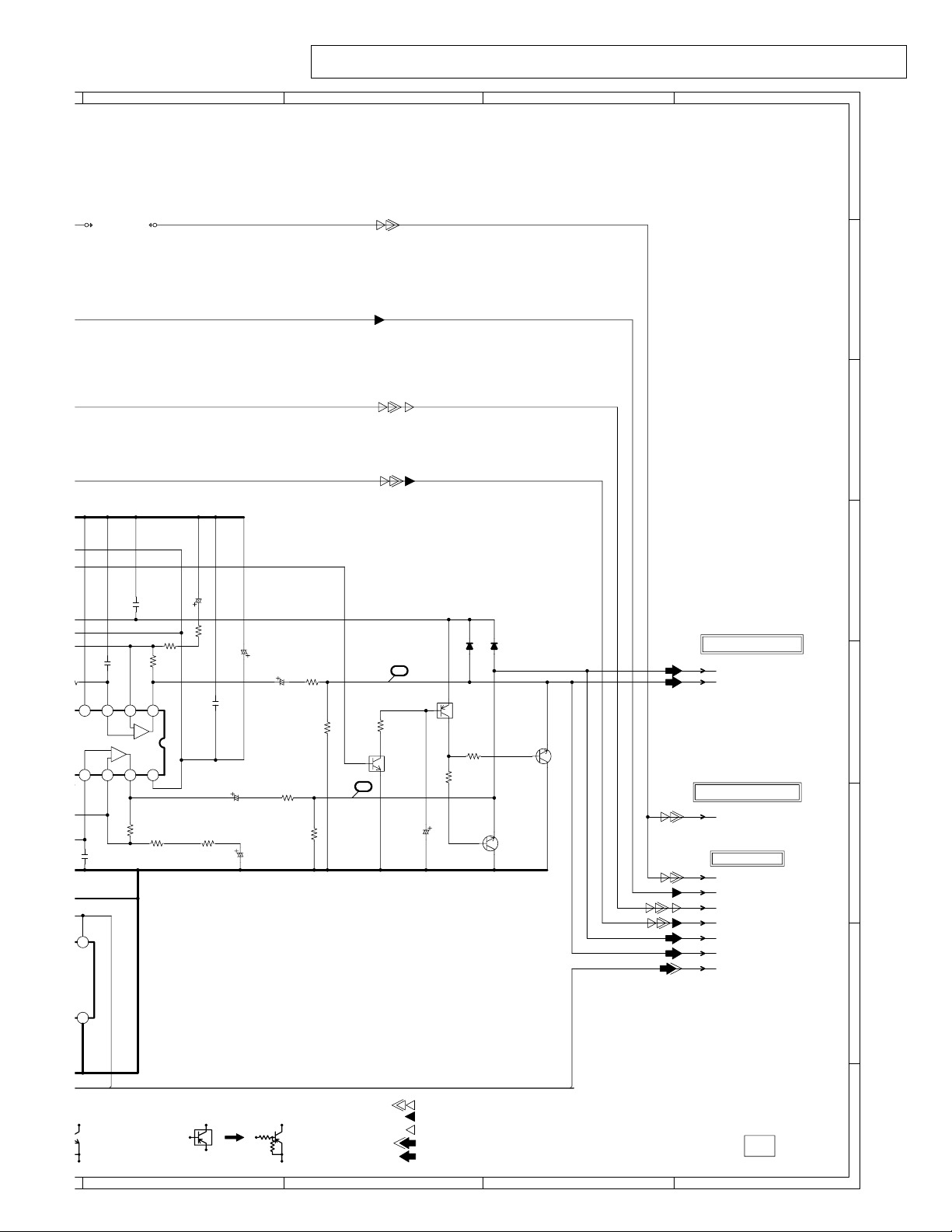
The Parts Number,value and rated voltage etc. in the Schematic Diagram are for references only.
C8043
Note :
When replacing the parts,refer to the Parts List.
EF GH
ATIC DIAGRAM
B)
S802X S802Y
8
DVD_V_OUT[DAC_D]
7
DVD_Y_VIDEO[DAC_A]
DVD_U[DAC_C]
6
DVD_V[DAC_B]
5
C8046
220P CH
C8044
100P CH
42
K
5.8 5.8 5.8
0
-
A_GND
5678
.8
B
0
9
BGND
8
+
+
-
11.65.85.8
12K
R8045
R8043
100P CH
CD/DVD
R8044
1234
VCC
10K
R8046
10K
12K
IC8003 NJM4580MAUDIO_AMP
C8048
R8049
R8050
100
2.250V YK
100
C8049
0.1 F
C8050
2216V MH7
C8051
C8052
D8014
5.0
C8022
5.0
-0.2
R8031
4.750V YK
D8015
MCL4148
MUTE SW.
Q8009
KRA101SRTK
R8024
1K
1K
-0.3
MCL4148
MUTE SW
Q8013
KTC3875S_Y_RTK
-0.3
MUTE SW
Q8012
KTC3875S_Y_RTK
0
0
0
0
10016V YK
C8061
R8027
2216V MH7
470
10K
R8051
R8053
470
10K
2.250V YK
R8034
10
3.3K
R8052
5.0
MUTE SW.
0
Q8008
KRC103SRTK
0
11
FROM/TO HI-FI/DEMODULATOR
DVD_A_OUT_L
DVD_A_OUT_R
FROM/TO Y/C/AUDIO/CCD/H.AMP
DVD_V_OUT[DAC_D]
FROM/TO TUNER/JACK
DVD_V_OUT[DAC_D]
DVD_Y_VIDEO[DAC_A]
DVD_U[DAC_C]
DVD_V[DAC_B]
DVD_A_OUT_L
DVD_A_OUT_R
SPDIF
4
3
2
OR
CAUTION: DIGITAL TRANSISTOR
PLAYBACK VIDEO SIGNAL
PLAYBACK LUMINANCE SIGNAL
PLAYBACK COLOR SIGNAL
DIGITAL AUDIO SIGNAL(PB)
AUDIO SIGNAL(PB)
PCBB00
VMB282
1
EF GH
2-26
Page 92

A B C D
8
9
P
P
8
7
OPERATION SCHEM
(OPERATION
(OPERATION
6
R6
SW685
REW/REV
R685
13K 1/4W
EVQ11L05R
PLAY
SW686
R686
6.8K 1/4W
EVQ11L05R
SW687
FF/CUE
R687
3.9K 1/4W
EVQ11L05R
SW688
REC/OTR
R688
2.7K 1/4W
EVQ11L05R
STOP
SW689
3.3K
EVQ11L05R
5
SW690
EVQ11L05R
OPEN/CLOSE
3.9K
R6
4
PCB270
VEBA07
3
2
NOTE:THE DC VOLTAGE EACH PART WAS
MEASURED WITH THE DIGITAL TESTER
DURING PLAYBACK.
1
A B C D
2-27
Page 93

The Parts Number,value and rated voltage etc. in the Schematic Diagram are for references only.
Note :
When replacing the parts,refer to the Parts List.
EF GH
MATIC DIAGRAM
PCB)
PCB)
DVD LED
R689
3.3K 1/4W
R690
3.9K 1/4W
D685
LTL-1CHGT-002A
FROM/TO OPERATION/DISPLAY
CP681
(CP651)
IMSA-9604S-05Z13
NC
DVD LED
GND
KEY-A
KEY-B
FFC
CD681
2H051202
5
4
3
2
1
8
7
6
5
NOTE:THIS SCHEMATIC DIAGRAM IS THE LATEST AT THE TIME
OF PRINTING AND SUBJECT TO CHANGE WITHOUT NOTICE
4
3
2
1
2-28
EF GH
Page 94

PRINTED CIRCUIT BOARDS
OPERATION
SOLDER SIDE
SW690
SW686
R690
R685
R686
SW689
SW685
R688
R687
SW687
SW688
D685
R689
CP681
2-29
Page 95

COMPONENT PARTS LOCATION GUIDE <VCR/DVD> VMB282A
REF.NO. LOCATION REF.NO. LOCATION REF.NO. LOCATION REF.NO. LOCATION REF.NO. LOCATION REF.NO. LOCATION REF.NO. LOCATION REF.NO. LOCATION REF.NO. LOCATION REF.NO.
CAPACITOR
C101_1 9I
C103 5D
C104 8I
C105 7E
C106 8I
C107 8H
C108 7E
C109 7E
C110 7I
C112 5I
C114 6I
C115 8E
C116 7E
C117 7E
C118 8E
C119 8D
C120 8D
C121 8E
C122 8E
C123 3G
C124 8E
C125 7F
C126 8F
C127 9D
C129 6D
C131 5G
C132 8F
C133 8G
C134 7H
C135 8G
C136 8G
C137 8G
C138 8G
C139 7F
C140 4H
C141 7G
C142 7H
C143 7G
C144 6G
C145 6G
C146 7G
C147 6G
C148 6H
C151 6G
C152 7G
C154 6F
C155 5G
C156 7F
C163 7E
C165 6E
C166 6F
C169 6E
C172 8H
C301 2B
C303 1C
C309 2B
C313 1F
C315 2B
C316 1D
C318 2B
C501 14B
C502 20C
C504_1 12B
C505 13C
C506 12C
C508 17B
C509 19B
C510 12B
C511_2 19E
C513 18C
C514_1 13C
C515 18C
C516 19B
C517 13C
C518_2 14D
C519_1 14C
C520 15E
C521_1 14B
C522 16D
C524 14A
C525 19C
C527 18B
C528_1 19B
C529 20E
C531 14B
C533 17F
C534 11C
C652 12O
C701 2E
C702 3F
C703 3E
C704 3E
C705 2E
C706 3E
C707 3E
C708 3E
C709 3D
C711 3D
C713 3D
C714 4D
C715 3D
C716 4D
C719 4D
C720 4D
C721 4D
C722 6E
C723 5E
C724 6D
C725 5D
C726 5D
C727 5D
C728 4E
C729 5E
C730 5E
C731 6E
C732 6E
C734 4G
C735 4G
C736 4G
C737 4F
C738 5F
C739 5F
C740 5F
C741 5F
C742 5E
C743 4G
C744 4G
C746 3G
C747 3G
C748 3G
C749 3F
C750 3F
C751 4F
C752 2F
C754 3G
C755 2E
C756 2F
C757 2B
C758 2F
C759 3F
C760 3F
C762 3E
C763 3E
C2002 18I
C2003 18I
C2006 17G
C2009 18I
C2015 19I
C2018 19I
C2019 19I
C2020 17I
C2021 19M
C2022 19L
C2023 19I
C2024 19J
C2027 17J
C2028 19J
C2032 20K
C2034 17K
C2036 21I
C2037 19K
C2038 18L
C2039 19L
C2041 17K
C2042 18K
C2043 19L
C2044 19L
C2045 19L
C2046 18L
C2047 21M
C2048 18K
C2049 21M
C2050 17L
C2051 17L
C2052 18L
C2053 21M
C2054 13K
C2055 13I
C2301 22K
C2304 22L
C2306 21L
C2307 22L
C2309_1 19N
C2310 20N
C2315 20M
C2601 21J
C2604 22I
C2605 21J
C2606 21J
C2607 21K
C2608 21G
C2609 21J
C2610 19G
C2612 20K
C2614 21G
C2615 22G
C2616 22G
C2617 22G
C2618 20G
C2619 21G
C2621 20H
C2622 21H
C2623 19H
C2624 21I
C2625 21H
C2626 20H
C2627 21H
C2628 20I
C2629 19H
C2631 20H
C2632 20I
C2633 20H
C2634 20H
C2635 21H
C2636 21I
C2637 20I
C2638 19I
C2640 19I
C2641_1 19G
C2642 19G
C2643 20I
C3001 7L
C3004 7M
C3005 1I
C3006 9K
C3007 8M
C3008 8N
C3009 6M
C3010 7K
C3013 11L
C3014 5N
C3015 7L
C3016 11L
C3017 9M
C3018 7L
C3019 8L
C3020 6M
C3021 5N
C3022 10L
C3023 5N
C3024 6M
C3025 6M
C3027 8L
C3029 12K
C3030 7O
C3031 8M
C3032 11L
C3033_1 15H
C3034 9L
C3036 9M
C3038 9L
C3040 16F
C3041 8L
C3044 8M
C3045 6N
C3046 6O
C3047 6O
C3049 8M
C3050 6M
C3052 12L
C3053 6M
C3061 8M
C3065 9L
C4001 12E
C4002 12E
C4003 11E
C4004 11F
C4005 13F
C4006 16G
C4007 12E
C4008 11F
C4009_1 15H
C4010 11E
C4011_1 16H
C4012 15H
C4013 12F
C4014 11F
C4015 15H
C4016 11G
C4017 11G
C4018 11G
C4020 16G
C4021 14H
C4022 15G
C4024 11G
C4026 13H
C4027 11G
C4028 14H
C4029 15G
C4030 13I
C4031 11H
C4032 12H
C4033 13H
C4034 11H
C4035 16G
C4036 18N
C4037 9E
C4038 14H
C4040 14H
C4041 13G
C4042 12H
C4043 9H
C4045_1 11D
C4046 11E
C4048 9G
C4049 9G
C4050 10E
C4051 10G
C4052 10G
C4053 10G
C4054 10F
C4055 9F
C4062 10H
C4063 10D
C4069 11E
C4070 12F
C4071 16F
C4072 12E
C4075 13G
C4076 12F
C4077 12G
C4084 13G
C4085 13F
C8010 6B
C8012 15F
C8013 4C
C8015 3B
C8019 3N
C8020 15F
C8021 15F
C8022 6C
C8023 7C
C8024 7C
C8025 11B
C8026 11A
C8027 12A
C8028 16F
C8029 16F
C8030 14F
C8031 5L
C8032 4L
C8033 13E
C8037 8B
C8038 9B
C8039 10B
C8041 6C
C8043 6C
C8044 6C
C8046 6B
C8048 8B
C8049 6C
C8050 5C
C8051 7C
C8052 6C
C8053 4L
C8054 6B
C8055 7C
C8057 4L
C8060 7C
C8061 5C
C8062 15F
C8063 14F
C8064 14F
C8065 14F
C8066 10D
C8067 10D
C8068 10D
C8069 10E
C8070 8C
C8071 8C
C8072_1 10D
C8075 3I
C8094 6B
C8095 6B
C8096 7B
C8097 7B
C8098 8A
C8099 3P
C8100 5P
CONNECTOR
CP101 7D
CP102 9D
CP103 1H
CP651 21O
CP2301 22K
CP2302 22L
CP2601 22J
CP3001 14G
DIODE
D502 22F
D503 21F
D504 19C
D505 22E
D506 20E
D507 15B
D509 17D
D510 20C
D511 14E
D512 14E
D513 13B
D514 12D
D515 15D
D518 15D
D522 15D
D523 16E
D524 18B
D525 14D
D530 18B
D531 19B
D532 15A
D534 14B
D535 16A
D536 14C
D537 14C
D538 14B
D539 14D
D651 6P
D656 15N
D701 5E
D702 3G
D2001 21M
D2601 21K
D2602 21K
D3001 9J
D3007 8K
D3009 6N
D8002 3O
D8004 8C
D8006 8C
D8007 7C
D8008 4H
D8011 9C
D8012 9B
D8013 10C
D8014 6B
D8015 5B
D8016 9C
D8017 9B
D8018 9B
FUSE
F501 22D
IC
IC101 8F
IC501 14A
IC502 13B
IC503 18A
IC701 4E
IC2001 18J
IC2002 18L
IC2003 21M
IC2004 17L
IC2301 20N
IC2601 20H
IC3001 8M
IC3003 6N
IC3099 7O
IC4001 12G
IC4002 12E
IC4003 15H
IC4005 9F
IC4007 11I
IC8003 6C
IC8004 10E
IC8005 4L
IC8006 10E
COIL
L101 8I
L102 7I
L105_1 6H
L106_1 6F
L107 6E
L301 1F
L501 20D
L505 13B
L506 14D
L701_1 4G
L702_1 4G
L703 3G
L3003 8L
L4001 16G
L4002 13H
L8001 9B
L8002 7B
L8003 9B
L8004 4L
L8005 15F
L8006 16F
L8007 8B
L8009 15F
L8010 14F
TRANSISTOR
Q101 8D
Q102 8E
Q103 8H
Q104 8H
Q105 5H
Q106 8H
Q107 8G
Q109 6G
Q301 1B
Q303 1E
Q501 18D
Q502 19C
Q503 11B
Q504 11C
Q505 13C
Q506 11C
Q507 13B
Q508 13B
Q509 13D
Q510 13D
Q511 12C
Q530 15A
Q531 15A
Q651 13N
Q652 13O
Q653 13O
Q654 13N
Q655 14O
Q656 14O
Q657 14O
Q658 14O
Q659 14N
Q660 14N
Q661 15O
Q662 14N
Q663 13N
Q664 13N
Q665 15O
Q666 19O
Q2602 21L
Q2604 21L
Q2605 21J
Q2606 21K
Q2608 21L
Q2609 21J
Q3001 6L
Q3002 11M
Q3003 9O
Q3004 14M
Q3005 13M
Q3006 1I
Q3007 9O
Q3008 16I
Q8001 7B
Q8002 7B
Q8003 4C
Q8004 4B
Q8005 5B
Q8006 5B
Q8007 5B
Q8008 6C
Q8009 6B
Q8010 8C
Q8011 7C
Q8012 5C
Q8013 5B
RESISTOR
R101 9H
R102 8E
R103 8D
R105 7D
R106 7E
R107 8I
R108 6H
R109 8E
R110 8E
R111 8E
R112 8E
R113 7E
R114 8E
R115 8E
R116 8E
R117 8E
R119 9D
R120 8H
R121 8H
R122 7F
R123 7G
R124 7G
R126 7H
R127 7G
R129 6G
R131 7G
R132 6G
R133 6G
R136 4I
R137 4H
R138 4K
R139 3K
R141 4I
R142 7E
R143 4I
R301 2B
R302 3C
R304 2B
R305 2B
R501 20B
R502 20D
R503 21E
R504 19B
R506 19E
R507 17B
R508 19C
R509 12C
R510 15A
R512 17D
R513 12D
R514 11C
R515 12C
R516 18C
R517 15E
R518 16B
R519 16B
R520 15B
R521 16B
R522 14A
R523 11C
R524 18B
R525 20B
R526 13B
R527 13B
R528 13B
R529 12B
R530 12B
R531 12B
R533 13D
R534 13D
R535 13D
R536 15E
R537 18C
R538 18C
R540 13B
R541 14D
R542 16A
R543 13B
R544 11C
R651 13O
R653 7P
R657 10P
R658 9P
R659 10O
R661 13N
R662 13O
R663 13O
R664 13N
R665 14O
R666 14O
R667 14O
R668 14O
R669 14N
R670 15O
R671 14N
R672 15P
R673 15O
R674 13N
R675 15N
R683 20O
R701 3E
R702 2D
R703 2E
R704 2D
R707 4D
R708 3D
R711 4D
R712 4D
R714 5F
R716 4G
R717 3G
R718 2F
R719 2E
R720 3F
R721 2E
R722 2D
R723 3H
R2003 18I
R2004 19I
R2006 18I
R2007 19L
R2011 19K
R2015 19K
R2016 19K
R2017 18K
R2018 18L
R2020 18L
R2025 19K
R2026 18L
R2028 17L
R2029 19K
R2031 21M
R2032 18L
R2033 21M
R2034 21M
R2035 18K
R2036 21M
R2037 21M
R2038 21M
R2302 21L
R2305 21L
R2307 21L
R2310 20M
R2311 21L
R2312 21L
R2313 21M
R2314 21L
R2317 20N
R2318 19N
R2319 19N
R2320 19M
R2321 19N
R2322 19N
R2323 19M
R2324 19M
R2605 21J
R2609 21J
R2610 20L
R2611 21K
R2612 21L
R2614 21K
R2615 21J
R2616 21L
R2617 21J
R2619 20G
R2620 20G
R2621 19H
R2622 19G
R2623 19G
R2624 21G
R2625 21G
R2626 19H
R2627 21J
R2628 19G
R2629 19G
R2630 21G
R2631 21G
R2633 22G
R2634 22G
R2635 21G
R2636 21G
R2637 19G
R2638 19G
R2639 21J
R2645 21G
R2647 20G
R2648 21G
R2652 20G
R2653 20H
R2654 21H
R2656 20I
R2657 19I
R2658 20H
R2659 19H
R2660 19H
R2661 21I
R2665 19H
R2666 21I
R2670 20I
R2671 20I
R2673 20I
R2675 20I
R2678 20I
R3001 7M
R3002 12L
R3003 14G
R3004 8K
R3006 12L
R3007 7K
R3008 8N
R3009 9N
R3010 8M
R3011 9N
R3012 7L
R3014 7M
R3015 9M
R3016 8J
R3017 7K
R3019 6L
R3020 7K
R3022 7L
R3024 7L
R3025 8M
R3026 1I
R3027 8L
R3028 8O
R3029 9O
R3030 10L
R3031 7M
R3032 7M
R3033 6M
R3034 6M
R3035 16F
R3037 5O
R3038 9M
R3043 8M
R3044 7O
R3045 8O
R3046 9M
R3047 9M
R3049 6M
R3050 14L
R3051 6N
R3053 8M
R3055 9M
R3056 8L
R3057 6M
R3062 6N
R3063 9L
R3083 14M
R3087 14L
R4001 14F
R4002 14F
R4003 13E
R4004 12E
R4006 11F
R4007 11F
R4008 13E
R4009 12F
R4012 12G
R4013 10H
R4014 11F
R4016 12E
R4017 12E
R4018 14G
R4019 10F
R4020 13F
R4021 13F
R4022 13F
R4024 10F
R4025 13F
R4026 10F
R4027 10F
R4028 13F
R4029 10F
R4030 13G
R4031 13G
R4032 15H
R4033 15H
R4034 15H
R4035 13G
R4036 13H
R4038 11H
R4039 10H
R4044 10H
R4049 11E
R4051 12F
R4052 11F
R4055 14F
R4056 14F
R4058 11E
R4059 13F
R4060 10H
R4062 13F
R4076 13H
R4078 13G
R8002 8C
R8003 6A
R8004 7B
R8005 7A
R8006 7B
R8007 7B
R8008 10B
R8009 4C
R8010 3B
R8011 5C
R8014 5B
R8015 5B
R8016 5C
R8017 5B
R8019 2P
R8020 10A
R8021 5C
R8023 10B
R8024 5B
R8025 9C
R8026 7C
R8027 5C
R8028 9B
R8029 9B
R8030 10B
R8031 5C
R8032 5B
R8033 7B
R8034 4C
R8035 7C
R8036 7C
R8037 7C
R8038 7C
R8039 6C
R8040 7C
R8041 6C
R8042 6C
R8043 7C
R8044 7C
R8045 7C
R8046 7C
R8049 7C
R8050 7C
R8051 4C
R8052 6C
R8053 5C
R8054 5C
R8055 5B
R8056 6B
R8059 3I
R8060 14F
R8061 13G
R8062 15F
R8063 14F
R8065 5B
R8067 5A
R8068 14F
R8069 9D
R8070 10D
R8071 11E
R8072 11E
R8073 11E
R8078 10A
SWITCH
SW651 11P
SW652 1P
SW653 9P
SW654 8P
SW655 7P
SW3001 4O
SW7001 10A
TEST POINT
TP101 2K
TP701 2K
TP3001 2K
TP3002 2K
TP8001 5B
OTHER
B2601 21I
B2602 17G
B4001 16G
B4002 15G
B4003 14H
B4004 16G
B4005 15G
B4006 15H
B4007 10D
B4008 10E
B4009 13H
B501 17C
B8001 6B
B8002 10D
B8003 10D
CD501_4 ?B
FH501 22C
FH502 22D
HS2301 20N
HS501 18E
J8001 5A
J8003 3P
J8004 4P
J8005 5P
J8006 9A
J8007 6A
J8008 12A
JG2001 20J
JG2002 19I
JG2003 19I
JG2004 17J
JG2005 17J
JG2006 20K
JG2007 20K
JG2008 18K
JG2009 18K
JG2010 17K
JG2601 21J
JG2602 21J
JG3001 7N
JG3002 4M
JG3003 11O
JG3004 10O
JG3005 5M
JG3006 4N
JG3007 4N
JG3008 5M
JG4001 13H
JG4002 12H
JG4003 12H
JG4004 12H
JG4005 13E
JG4006 13H
JG4007 11E
JG4008 11E
JG4009 17K
JG4010 11E
JG4011 12E
JG4012 12E
JG4013 14F
OS651 12P
OS8001 7B
S501 21B
S502 20C
S801X 7I
S801Y 3B
S802X 14F
S802Y 9I
T501 17C
TU301 1B
V651 13P
X101 6G
X2001 19K
X3001 6M
X3002 6N
X4001 13G
2-30
Page 96

5
R509
C5 0
C
W821
B
S
1
L301
W810
CP103
C313
TU301
C315
C309
C318
C752
Q3006
C758
W004
R302
C705
C756
C123
L703
C703
C759
S801Y
C709
C706
C702
C754
C750
C747
R723
C711
C704
C8015
C8075
C708
D702
C713
Q8004
C714
L702_1
D8008
C743
R8009
C735
TP8001
C719
R137
C140
C8013
L701_1
Q8007
C720
C728
C737
J8001
C8050
C727
Q8005
R8021
C739
W809
Q105
D701
W837
Q8006
R8016
W002
C741
R8054
W001
W838
R8017
C8061
C103
C740
C742
C112
R8032
R8055
C131
J8007
R8056
W011
W835
D8014
C8022
C8052
W013
W003
L105_1
C8046
L106_1
X101
R8042
C8044
C8043
W014
L107
C8054
R8039
R8004
C8041
IC8003
R8041
CP101
C148
C8094
C151
S801X
R8005
R8006
R8044
R8043
R8045
R8038
C163
Q8002
R8050
R8037
C156
C146
C110
Q8001
L8002
C8060
C142
C8024
W012
C152
R8007
R8046
C108
R106
R123
OS8001
R8049
C8023
C8051
C139
L102
C8097
R8036
C105
C117
C143
C125
R124
R8035
C116
L8007
C8055
C115
R122
Q106
Q104
R109
R110
C121
C172
C8048
C119
L101
R103
R102
R112
C137
R111
R117
R116
C126
C8070
C120
C118
R120
C8037
R114
C138
R121
C104
C122
C136
PRINTED CIRCUIT
VCR/DVD (TOP
IC8004
IC4005
C8072_1
R8070
R4013
SW7001
C8067
C4050
C4051C4052 C4053C4054
W804
C4062
C4063
C8069
R4024
R4026
R4039
R4060
C8071
C124
C135
J8006
R8028
C101_1
C8038
CP102
L8003
L8001
R8069
C4055
C4048C4049
D3001
C8039
IC8006
C8068
R4049
C4045_1
C4069
C4004
IC4007
J8008
R4058
C4007
C4003
C506
R515
C4042
IC4001
IC4002
C4001
R4004
Q503
Q504
R514
R544
W858
R8071
R8072
R8073
53
105
SW652
TP701
TP3001
TP101
TP3002
W007
W006
C8019
D8002
J8003 J8004
C8053
W008
L8004
SW3001
C8032
J8005
C8031
W010
W005
C3023
W009
C3021
Q3001
D3009
D651
C3045
X3001
X3002
W839
W840
IC3099
SW655
C3015
R3022
R3012
C3004
R3032
R3024
R3014
R3031
C3018
C3007
R3001
L3003
R3025
C3044
C3031
C3008
SW654
D3007
R3010
R3053
C3061
R3008
C3041
R3027
R3043
C3049
C3019
R3056
C3065
C3036
R3046
R3047
R3015
R3011
Q3003
R3055
R3038
R3009
SW653
W019
Q3007
R3029
W802
C3032
SW651
1110987654321
C3016
C3013
Q3002
C3029
C3052
OS6
2-31
Page 97
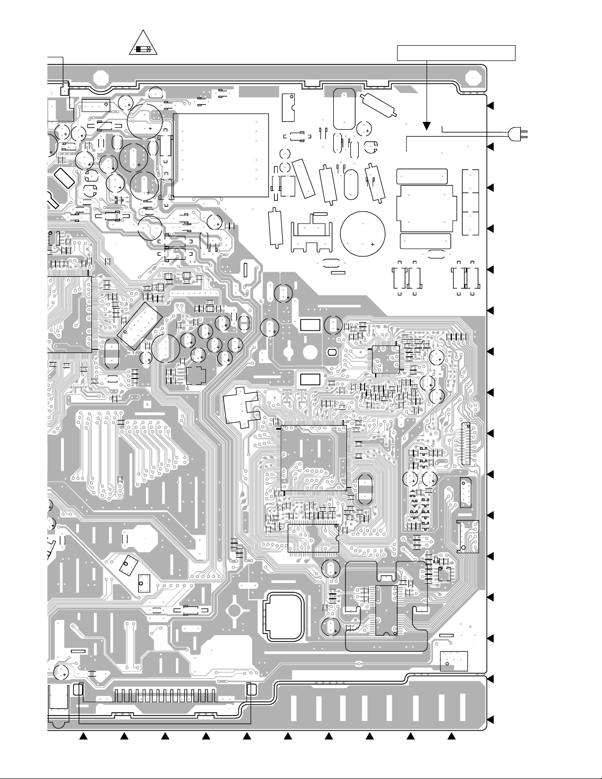
8
BOARDS
P SIDE)
CAUTION :
FOR CONTINUED PROTECTION AGAINST FIRE HAZARD,REPLACE ONLY WITH SAME TYPE AND RATED FUSE(S).
T
ATTENTION :
REPLACER PAR DES FUSIBLE DE MEME TYPE.
DANGEROUS V OL T A GE
C2617
CP2601
CP2301
FH501
F501
FH502
D502
CP2302
A
B
CD501_4
C
D
E
F
G
H
I
J
K
L
M
N
IC501
C521_1
008
07
C4001
042
C3052
2
IC4002
C4001
R509
R4004
C4032
C510
Q511
R4016
R3002
W849
R4017
C4002
D514
C504_1
R533
C4033
R513
R4003
1
157
R528
Q505
Q510
R4008
R4076
IC502
C517
R527
D513
C4085
R4062
L505
C514_1
D525
C8033
R4021
R4059
R4035
R4078
L4002
X4001
C505
C4030
C2055
Q509
R4020
C2054
Q3005
R8061
R3050
C4038
C4028
C4021
C519_1
C501
C531
C518_2
D539
R541
L506
C8030
R8063
C8064
CP3001
R3003
C4040
Q3004
R671 D656
C8063
R8068
L8009
L8010
C8065
D534
D507
D515
C8062
D511
D512
C3033_1
R4033
R4032 R4034
C4012
D522
D518
L8005
C8012
W895
C4029
C4015
D532
C8020
R8062
W866
IC4003
R517
C8028
C8021
C4022
C4009_1
L8006
D523
C522
C4035
D535
C8029
T501
C4020
C4011_1
Q3008
W850
W803
W813
W903
R3035
C4006
W825
W827
W906
L4001
R512
C2006
C2051
C2050
D509
C2020
C2034
R2028
C2041
IC2004
B501
C533
89
IC503
C513
C2042
D530
R2026
C515
HS501
Q501
IC2001
C2048
C2046
R2035
R2032
W806
R2017
R2018
R516
R2020
IC2002
C4036
D524
R2006
R506
R2621
R2003
C2038
R2324
R2323
R2322
W823
C2641_1
C2019
R2015
C2043
C2021
C2309_1
C509
C2018
145
133
D504
R2626
R2029
C516
D531
R2629
C2037
R2016
B2001
C2045
C525
C2023
R2319
R504
C2610
R2638
R2660
R2004
C2024
C2028
C511_2
R2622
R2637
R2628
R2025
R2623
C2629
C2039
R2320
C528_1
Q502
D510
C2638
X2001
C2044
R2657
C2640
R2318
33
W885
R2671
R2673
IC2601
C2634
R2675
R502
C2628
IC2301
R501
C2631
R2656
C2618
117
49
C2315
D506
R2647
R2654
R2658
C2637
W886
W889
C2621
R2653
W826
C2625
R2670
R2605
D2601
R2310
C2633
R2661
R2627
C2612
D2602
Q2602
R2610
R2313
D503
R2645
W883
R2616
R2302
R2307
R2305
C2047
R2034
R2033
R2031
R2037
C502
R2648R2652
C2635
R2666
C2636
Q2605
R2609
R2617
R2614
R2612
C529
Q2609
Q2606
Q2608
Q2604
R2036
L501
R2611
C2619
C2608
C2627
R503
C2606 C2609
C2607
C2622
C2624
R2615
D2001
R2639
C2053
R2038
IC2003
C2614
C2615
D505
C2616
OS651
W021
C652
2-32
R651
V651
HS2301
W023
CP651
O
P
2221201918171615141312
Page 98

C
R4007
4
PRINTED CIRC
U
T
VCR/DVD (BO
R3026
C3005
R8019 C8099
R139
R8059
C8057
R136
IC8005
R138
R141
R143
C8100
C3014
R3037
R3051
C3025
C3050
R3049
R3062
IC3003
C3024
R3033
C114
C3047
C3053
R3019
C3046
C3009
C3020
R108
R3034
R3057
R653
R3044
C3030
R3017
R3007
C3010
C3001
R3020
IC3001
C3027
R3045
R3028
C107
C106
R107
Q103
R3004
R3016
C3034
R3063
C3006
R101
C3038
C3017
S802Y
R658
R657
R659
C3022
R3030
Q303
C316
Q301
C303
C757
R304
R305
R301
C301
R719
C755
R722
R702
C701
R703
R721
R718
R704
C762
C763
C748
R701
C760
C707
R720
R708
C746
R717
C749
C715
R8010
C751
R707
C744
R716
C734
C716
Q8003
IC701
C736
R712
R8051
R711
C721
W845
R8034
R8011
R8053
C726
C155
R132 R127
C738
R714
C730
C731
C729
C722
C723
C725
R8027
Q8012
R8031
Q8013
R8024
D8015
Q8009
R8065
R8015
R8014
R8067
C724
C144
C129
Q109
R129
C732
C166
C165
C145
R8052
C154
C169
C8049
Q8008
B8001
C8010
C147
R133
C8095
R8003
R142
R126
R131
R8026
C8096
C109
Q8011
D8007
R105
C141
R113
R8040
R8033
C134
Q107
IC101
D8004
C8098
Q8010
C133
R115
R8002
Q101
Q102
W908
D8006
C132
R8025
C127
D8012
R8029
R119
C4043
D8011
D8017
D8016
B4008
C4037
C8066
D8018
R8078
R4019
B8002
R8023
R8008
R4029
R4027
D8013
R8030
R8020
B4007
R4044
B8003
C4027
C4024
C4018
C4017
C4016
C4014
C4008
C4010
R4038
R4052
C534
Q506
R523
R401
C4046
C4034
C4031
2-33
1110987654321
Page 99

CUIT BOARDS
OTTOM SIDE)
Q652
R674
Q664
Q651
R661
R664
Q663
Q653
Q654
R662
R663
Q655
R669
R665
P
R672
Q658
R667
R668
R670
Q661
R673
Q665
R675
Q666
R2321
R2317
R683
O
C2310
N
R666
Q656
Q657
Q660Q662
Q659
4052
R4014
C4046
C4034
C4031
R4007
R4006
C4013
W848
R4012
C4077
C4072
W863
R4009
C4070
W865
R3006
R4051
C4076
B4009
C4075
C4084
C4005
C4041
R4031
W808
R4022
R535
R4025
R4028
R534
C4026
R4030
R4036
R4018
R4055
R3087
B4003
R4056
R3083
R4001
S802X
R8060
R4002
R536
B4006
B4005
C520
B4002
B4004
B4001
C4071
C3040
B2602
C2027
C2003
W856
C2052
C2002
C2009
C2015
C2022
W860
R2007
R2011
R2665
R2659
C2623
C2642
C2032
C2643
R2620
R2619
C2632
W900
R2678
C2626
R2312
R2314
R2311
R2631
C2601
C2036
C2605
R2624R2630
R2625
C2049
B2601
R2636
C2306
C2307
C2301
R2633R2635
R2634
C2304
C2604
M
L
K
J
I
H
G
F
E
D
R508
R537
D538
R522
D536
C524
D537
Q530
Q531
R510
R519
R518
R520
R521
R542
R507
C508
506
523
C8025
C8026
C8027
R530
R529
R531
Q507
Q508
R526
R540
R543
C527
R524
R538
R525
C
B
A
22212019181716151413121
DANGEROUS V OL T A GE
2-34
Page 100

WAVEFORMS
MPEG/MICON
2ns
1.0V
1
20ns
500mV
2
MEMORY
500µs
500mV
3
READ CHANNEL
200ns
200mV
8
200ns
200mV
9
AUDIO/VIDEO
PB
500us
1.0V
10
PB
1ms
100mV
18
PB
200ms
500mV
19
REC
5µs
20V
20
DSP
20ns
1.0V
5
20ns
500mV
6
20ns
1.0V
7
PB
500us
1.0V
11
Y/C/AUDIO/CCD/HEAD AMP
PB
10µs
500mV
16
PB
100ns
100mV
17
VCR SYSCON
PB
5ms
1.0V
21
PB
200µs
1.0V
22
POWER ON
50ns
1.0V
23
NOTE: The following waveforms were measured at the point of the
corresponding balloon number in the schematic diagram.
2-35
 Loading...