

Page 1
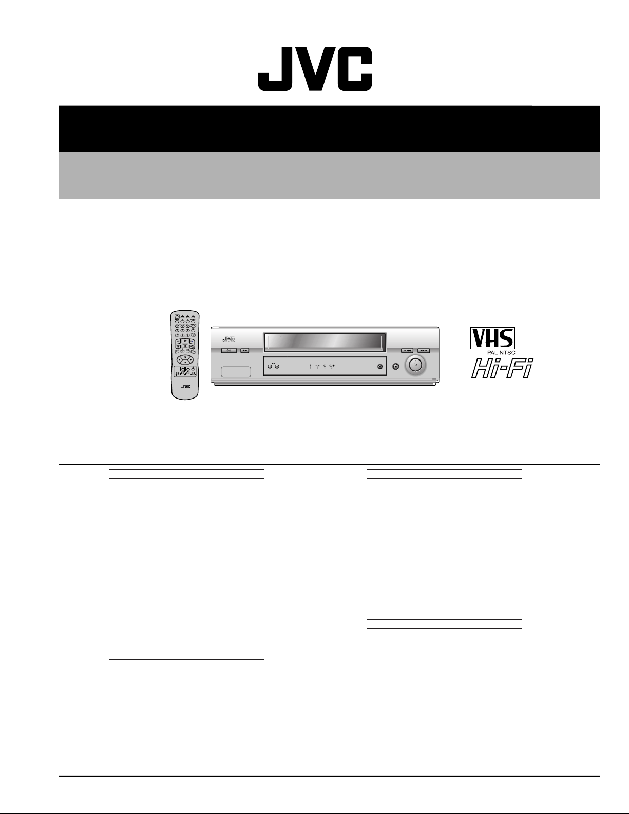
SERVICE MANUAL
VIDEO CASSETTE RECORDER
HR-J291EA, HR-J291MS,
HR-J297MS, HR-J695EA
Regarding service information other than these sections, refer to the service manual No. 82915 (HR-J290EU).
Also, be sure to note important safety precautions provided in the service manual.
SPECIFICATIONS
GENERAL
Power : 110 V – 240 Vd, 50 Hz/60 Hz
Power consumption
Power on : Approx. 12 W
Standby mode : 3.0 W
Video Head system
HR-J695EA : DA4 (Double Azimuth) head helical
HR-J291EA : Rotary two-head helical scan system
Tape speed
(SP) : 23.39 mm/sec
(LP) : 11.69 mm/sec
Tape format : Tape width 1/2"
Maximum recording time
(SP) : 240 min. with E-240 video cassette
(LP) : 480 min. with E-240 video cassette
Rewind time : Approx. 180 (±30) sec. with E-180
Dimensions (W x H x D) : 360 mm x 94.5 mm x 270 mm
Weight : 4.0 kg
Operating temperature : 5°C to 35°C
Operating humidity : Less than 80 %
Timer : 24 hours display type
VIDEO
Signal system : PAL-type colour signal and CCIR
Recording Format : PAL/MESECAM/NTSC 3.58/
RF reception
HR-J695EA : PAL B/G, SECAM D/K
HR-J291EA : PAL B/G
RF OUT : PAL B/G
RF modulator : UHF channels 22 – 68 (Adjustable)
Input level : VIDEO IN (RCA type)
Output level : VIDEO OUT (RCA type)
Signal-to-noise ratio : More than 43 dBm
(The specifications shown pertain specifically to the model HR-J291EA, HR-J695EA.)
AUDIO
scan system
(12.7 mm high density VHS tape)
cassette
monochrome signal, 625 lines
50 fields
NTSC 4.43
1.0 Vp-p, 75 Ω, unbalanced
1.0 Vp-p, 75 Ω, unbalanced
Input level : AUDIO IN (RCA type)
Output level : AUDIO OUT (RCA type)
Audio track
HR-J695EA : Mono track and Hi-Fi track
HR-J291EA : Mono track
Audio frequency response
Normal audio : 100 Hz to 10,000 Hz
Hi-Fi audio* : 20 Hz to 20,000 Hz
* HR-J695EA only
Audio signal to noise ratio
Normal audio : More than 43 dB (JIS A filter)
Hi-Fi audio* : More than 70 dB (JIS A filter)
* HR-J695EA only
Audio dynamic range [HR-J695EA only]
Hi-Fi audio : More than 85 dB (JIS A filter)
ACCESSORIES
Provided accessories : RF cable,
Specifications shown are for SP mode unless specified otherwise.
E. & O.E. Design and specifications subject to change without
notice.
–6.0 dBm, more than 47 kΩ
–6.0 dBm, less than 1 kΩ
(–6/+3 dBm)
(–3/+3 dBm)
Infrared remote control unit,
“R3” battery x 2
HR-J291EA,HR-J291MS,HR-J297MS,HR-J695EA V15A1/A11/D1
This service manual is printed on 100% recycled paper.
COPYRIGHT © 2002 VICTOR COMPANY OF JAPAN, LTD
No.82940
August 2002
Page 2

TABLE OF CONTENTS
SECTION 1
SUMMARY
KEY TO ABBREVIATIONS . . . . . . . . . . . . . . . . 1-1
IMPORTANT SAFETY PRECAUTIONS . . . . . . . . 1-2
PROPOSAL FOR APPL YING SHORT
PROTECTION . . . . . . . . . . . . . . . . . . . . . . . . . . .1-4
SERVICE NOTICE ON REPLACING EEPROM . .1-5
SERVICE INFORMATION FOR EEPROM
IC SETTING . . . . . . . . . . . . . . . . . . . . . . . . . . . .1-6
SPECIFICATIONS . . . . . . . . . . . . . . . . . . . . . . . 1-7
SECTION 2
CABINET & MAIN CHASSIS
SERVICE METHOD . . . . . . . . . . . . . . . . . . . . . 2-1
EXPLODED VIEWS . . . . . . . . . . . . . . . . . . . . . . 2-2
1. Cabinet & Main Frame Section . . . . . . . . . . . . . 2-2
2. Packing & Accessory Section . . . . . . . . . . . . . . 2-3
CIRCUIT DIAGRAMS . . . . . . . . . . . . . . . . . . . .3-30
1. Power Circuit Diagram . . . . . . . . . . . . . . . . . . . .3-30
2. Tuner, NICAM, A2 Circuit Diagram . . . . . . . . . . .3-32
3. A/V Circuit Diagram . . . . . . . . . . . . . . . . . . . . . .3-34
4. System Circuit Diagram . . . . . . . . . . . . . . . . . . .3-36
5. Hi-Fi Circuit Diagram . . . . . . . . . . . . . . . . . . . . .3-38
• WAVEFORM . . . . . . . . . . . . . . . . . . . . . . . . . . . .3-40
• CIRCUIT VOLTAGE CHART . . . . . . . . . . . . . . . .3-42
PRINTED CIRCUIT BOARD DIAGRAMS . . . . .3-46
1. MAIN P.C.Board . . . . . . . . . . . . . . . . . . . . . . . .3-46
SECTION 4
MECHANISM
Refer to the service manual No.82915 (HR-J290EU).
SECTION 5
REPLACEMENT PARTS LIST
SECTION 3
ELECTRICAL
ELECTRICAL ADJUSTMENT POINTS
ARRANGEMENT . . . . . . . . . . . . . . . . . . . . . . . .3-1
ELECTRICAL ADJUSTMENT PROCEDURES . . 3-2
1. Servo Circuit . . . . . . . . . . . . . . . . . . . . . . . . . . . 3-2
ELECTRICAL TROUBLESHOOTING GUIDE . . . 3-4
1. Power Circuit(SMPS) . . . . . . . . . . . . . . . . . . . . . 3-4
2. Servo Circuit . . . . . . . . . . . . . . . . . . . . . . . . . . .3-7
3. System & Front Panel Circuit . . . . . . . . . . . . . . .3-10
4. Y/C Circuit . . . . . . . . . . . . . . . . . . . . . . . . . . . . .3-13
5. Tuner/IF Circuit . . . . . . . . . . . . . . . . . . . . . . . . .3-17
6. Hi-Fi Circuit . . . . . . . . . . . . . . . . . . . . . . . . . . . .3-20
BLOCK DIAGRAMS . . . . . . . . . . . . . . . . . . . . .3-22
1. Power Block Diagram . . . . . . . . . . . . . . . . . . . .3-22
2. Tuner/IF, NICAM & A2 Block Diagram . . . . . . . .3-24
3. Y/C Block Diagram . . . . . . . . . . . . . . . . . . . . . .3-26
4. Hi-Fi Block Diagram . . . . . . . . . . . . . . . . . . . . .3-27
5. System Block Diagram . . . . . . . . . . . . . . . . . . .3-28
5.1 EXPLODED VIEW. . . . . . . . . . . . . . . . . . . . . . . .5-1
5.2 REPLACEMENT PARTS LIST. . . . . . . . . . . . . . .5-4
Page 3

SECTION1 SUMMARY
KEY TO ABBREVIATIONS
A AC :Alternating Current
B B :Base
C C :Capacitor, Chroma, Collector
D D :Drum, Digital, Diode, Drain
E E :Emitter
F F :Fuse
G GEN :Generator
H H :High, Horizontal
I IC :Integrated Circuit
L L :Low, Left, Coil
ACC :Automatic Color Control
ACSS :Automatic Channel Setting System
ADJ :Adjust
A/E :Audio Erase
AFC :Automatic Frequency Control
AFT :Automatic Fine Tuning
AGC :Automatic Gain Control
A.H.SW :Audio Head Switch
ALC :Automatic Level Control
AM :Amplitude Modulation
AMP :Amplifier
ANT :Antenna
APC :Automatic Phase Control
ASS’Y :Assembly
AUX :Auxiliary
BGP :Burst Gate Pulse
BPF :Bandpass Filter
BS :Brodcasting Satellite
BW or B/W :Black and White
CAN :Cancel
CAP :Capstan
CAP.BRK :Capstan Brake
CAP.RVS :Capstan Reverse
CATV :Cable Television
CBA :Circuit Board Assembly
CCD :Charge Coupled Device
C.CTL :Chro Control, Capstan Control
CFG :Capstan Frequency Generator
CHROMA :Chrominance
CNR :Chroma Noise Redution
COMB :Combination
COMP :Comparator
CONV :Converter
C.ROT SW :Color Rotary Switch
CS :Chip Selcet
C.SYNC :Composite Synchronization
CTL DIV :Control Divide
CUR :Current
CYL :Cylinder
D.ADJ :Drum Adjust
DC :Direct Current
D.CTL :Drum Control
DEMOD :Demodulator
DET :Detector
DEV :Deviation
DHP :Double High Pass
DIGITRON :Digital Display Tube
DL :Delay line
DOC :Drop Out Compensator
DUB :Dubbing
D.V SYNC :Dummy Vertical Synchronization
EE :Electric to Eletric
EMPH :Emphasis
ENA :Enable
ENV :Envelope
EP :Extended Play
EQ :Equalizer
EXP :Expander
FB :Feed Back
FBC :Feed Back Clamp
FE :Full Erase
FG :Frequency Generator
FL :Filter
FM :Frequency Modulation
F/R :Front/Rear
FS :Frequency Synthesizer
FSC :Subcarrier Frequency
F/V :Frequency Voltage
IF :Intermediate Frequency
INS :Insert
LD :LED
LD VTG CTL
LECHA :Letter Character
L.M :Level Meter
LP :Long Play
Comb Filter
Composite
Compensation
:Loading Voltage Control
M MAX :Maximum
N NR :Noise Reduction
O OSC :Oscillator
P PB :Playback
Q Q :Transistor
R R :Resistor, Right
S S :Serial
T T :Coil
U UHF :Ultra High Frequency
V V :Volt, Vertical
W W :Watt
X X-TAL :Crystal
Y Y/C :Luminance/Chrominance
Z ZD :Zener Diode
LPF :Low Pass Filter
MD :Modulator
MECHA.CTL
MIC :Microphone
MIN :Minimum
MIX :Mixer, Mixing
M.M. :Monostable, Multivibrator
MMV :Mono Multi Vibrator
MOD :Modulation, Modulator
MODEM :Modulator-Demodulator
MPX :Multiplex
OSD :On Screen Display
PCB :Printed Circuit Board
P.CTL :Power Control
PRE-AMP :Preamplifier
P.F :Power Failure
PG :Pulse Generator
PLL :Phase Locked Loop
PREM.DET :Premire Detect
P.P :Peak-to-Peak
PS :Phase Shift
PWM :Pulse Width Modulation
PWR CTL :Power Control
QH :Quasi Horizontal
QSR :Quick Setting Record
QTR :Quick Timer Record
QV :Quasi Vertical
RE(or RC) :Remocon, Receiver
REC :Recording
REC S ‘H’ :Record Start ‘Hight’
REF :Reference
REG :Regulated, Regulator
REMOCON :Remote Control(unit)
RF :Radio Frequency
R/P :Record/Playback
RTC :Reel Time Counter
S.ACCEL :Slow Accel
SAOP :Second Audio Program
SC :Scart, Simulcast
S.DET :Secam Detect
SH :Shift
SHARP :Sharpness
SIF :Sound Inter mediate Frequency
SLD :Side Locking
S/N :Signal to Noise Ratio
SP :Standard Play
ST :Stereo
SUB :Subtract, Subcarrier
SW or S/W :Switch
SYNC :Synchronization
SYSCON :System Control
TP :Test Point
TR :Transistor
TRK :Tracking
TRANS :Transfor mer
TU :Tuner, Take-up
UNREG :Unregulated
VA :Always Voltage
VCO :Voltage Controlled Oscillator
VGC :Voltage Gain Control
VHF :Very High Frequency
V.H.SW :Video Head Switch
VISS :VHS Index Search
VPS :Video Program System
VR :Variable Resistor or Volume
V-SYNC :Vertical Synchronization
VTG :Voltage
VV :Voltage to Voltage
VXO :Voltage X-tal Oscillator
WHT :White
W/O :With out
YNR :Luminance Noise Reduction
:Mechanism Control
1-1
Page 4
Important Safety Precautions
cut close to connector
Prior to shipment from the factory, JVC products are strictly inspected to conform with the recognized product safety and electrical codes
of the countries in which they are to be sold. However, in order to maintain such compliance, it is equally important to implement the
following precautions when a set is being serviced.
v
Precautions during Servicing
1. Locations requiring special caution are denoted by labels and
inscriptions on the cabinet, chassis and certain parts of the
product. When performing service, be sure to read and comply with these and other cautionary notices appearing in the
operation and service manuals.
2. Parts identified by the symbol and shaded ( ) parts are
critical for safety.
Replace only with specified part numbers.
Note: Parts in this category also include those specified to com-
ply with X-ray emission standards for products using
cathode ray tubes and those specified for compliance
with various regulations regarding spurious radiation
emission.
3. Fuse replacement caution notice.
Caution for continued protection against fire hazard.
Replace only with same type and rated fuse(s) as specified.
4. Use specified internal wiring. Note especially:
1) Wires covered with PVC tubing
2) Double insulated wires
3) High voltage leads
5. Use specified insulating materials for hazardous live parts.
Note especially:
1) Insulation Tape 3) Spacers 5) Barrier
2) PVC tubing 4) Insulation sheets for transistors
6. When replacing AC primary side components (transformers,
power cords, noise blocking capacitors, etc.) wrap ends of
wires securely about the terminals before soldering.
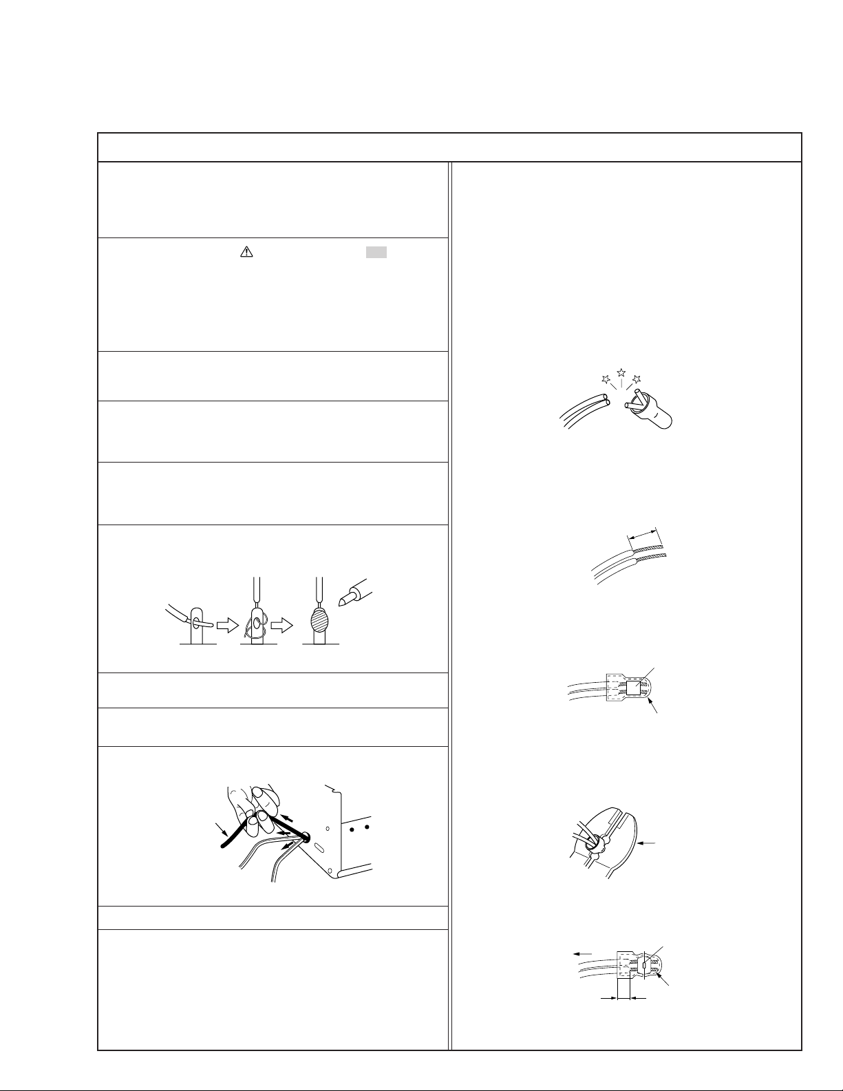
12. Crimp type wire connector
In such cases as when replacing the power transformer in sets
where the connections between the power cord and power
transformer primary lead wires are performed using crimp type
connectors, if replacing the connectors is unavoidable, in order to prevent safety hazards, perform carefully and precisely
according to the following steps.
1) Connector part number : E03830-001
2) Required tool : Connector crimping tool of the proper type
which will not damage insulated parts.
3) Replacement procedure
(1) Remove the old connector by cutting the wires at a point
close to the connector.
Important : Do not reuse a connector (discard it).
Fig.3
(2) Strip about 15 mm of the insulation from the ends of
the wires. If the wires are stranded, twist the strands to
avoid frayed conductors.
15 mm
Fig.1
7. Observe that wires do not contact heat producing parts
(heatsinks, oxide metal film resistors, fusible resistors, etc.)
8. Check that replaced wires do not contact sharp edged or
pointed parts.
9. When a power cord has been replaced, check that 10-15 kg of
force in any direction will not loosen it.
Power cord
Fig.2
10. Also check areas surrounding repaired locations.
11. Products using cathode ray tubes (CRTs)
In regard to such products, the cathode ray tubes themselves,
the high voltage circuits, and related circuits are specified for
compliance with recognized codes pertaining to X-ray emission.
Consequently, when servicing these products, replace the cathode ray tubes and other parts with only the specified parts.
Under no circumstances attempt to modify these circuits.
Unauthorized modification can increase the high voltage value
and cause X-ray emission from the cathode ray tube.
Fig.4
(3) Align the lengths of the wires to be connected. Insert
the wires fully into the connector.
Metal sleeve
Connector
Fig.5
(4) As shown in Fig.6, use the crimping tool to crimp the
metal sleeve at the center position. Be sure to crimp fully
to the complete closure of the tool.
1.25
2.0
5.5
Fig.6
(5) Check the four points noted in Fig.7.
Not easily pulled free
Wire insulation recessed
more than 4 mm
Fig.7
Crimping tool
Crimped at approx. center
of metal sleeve
Conductors extended
1
S40888-01
Page 5
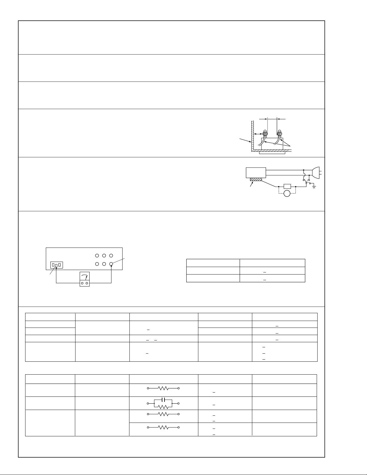
v
Safety Check after Servicing
Examine the area surrounding the repaired location for damage or deterioration. Observe that screws, parts and wires have been
returned to original positions, Afterwards, perform the following tests and confirm the specified values in order to verify compliance with safety standards.
1. Insulation resistance test
Confirm the specified insulation resistance or greater between power cord plug prongs and
externally exposed parts of the set (RF terminals, antenna terminals, video and audio input
and output terminals, microphone jacks, earphone jacks, etc.). See table 1 below.
2. Dielectric strength test
Confirm specified dielectric strength or greater between power cord plug prongs and exposed
accessible parts of the set (RF terminals, antenna terminals, video and audio input and output
terminals, microphone jacks, earphone jacks, etc.). See table 1 below.
3. Clearance distance
When replacing primary circuit components, confirm specified clearance distance (d), (d’) between soldered terminals, and between terminals and surrounding metallic parts. See table 1
below.
Chassis
Fig. 8
4. Leakage current test
Confirm specified or lower leakage current between earth ground/power cord plug prongs
and externally exposed accessible parts (RF terminals, antenna terminals, video and audio
input and output terminals, microphone jacks, earphone jacks, etc.).
Measuring Method : (Power ON)
Insert load Z between earth ground/power cord plug prongs and externally exposed accessible parts. Use an AC voltmeter to measure across both terminals of load Z. See figure 9 and
following table 2.
5. Grounding (Class 1 model only)
Confirm specified or lower grounding impedance between earth pin in AC inlet and externally exposed accessible parts (Video in,
Video out, Audio in, Audio out or Fixing screw etc.).
Measuring Method:
Connect milli ohm meter between earth pin in AC inlet and exposed accessible parts. See figure 10 and grounding specifications.
AC inlet
Earth pin
Exposed accessible part
Grounding Specifications
Region
USA & Canada
Europe & Australia
Externally
exposed
accessible part
Grounding Impedance (Z)
d
d'
≤
Z 0.1 ohm
≤
Z 0.5 ohm
Power cord,
primary wire
Z
V
Fig. 9
ab
c
Milli ohm meter
Fig. 10
AC Line Voltage
100 V
100 to 240 V
110 to 130 V
110 to 130 V
200 to 240 V
100 V
110 to 130 V
110 to 130 V
220 to 240 V
Note: These tables are unofficial and for reference only. Be sure to confirm the precise values for your particular country and locality.
Region
Japan
USA & Canada
Europe & Australia R 10 MΩ/500 V DC
Region Load Z
Japan
USA & Canada
Europe & Australia
Table 2 Leakage current specifications for each region
Insulation Resistance (R)
≤
R 1 MΩ/500 V DC
≥≥
1 MΩ R 12 MΩ/500 V DC
≤
Table 1 Specifications for each region
1 kΩ
0.15 µF
1.5 kΩ
2 kΩ
50 kΩ
Dielectric Strength
AC 1 kV 1 minute
AC 1.5 kV 1 miute
AC 1 kV 1 minute
AC 3 kV 1 minute
AC 1.5 kV 1 minute
i 1 mA rms Exposed accessible parts
i 0.5 mA rms
i 0.7 mA peak
i 2 mA dc
i 0.7 mA peak
i 2 mA dc
2
≤
≤
≤
≤
≤
≤
(Class 2)
(Class 1)
Clearance Distance (d), (d')
≤
d, d' 3 mm
≤
d, d' 4 mm
≤
d, d' 3.2 mm
≤
d 4 mm
≤
d' 8 mm (Power cord)
≤
d' 6 mm (Primary wire)
a, b, cLeakage Current (i)AC Line Voltage
Exposed accessible parts
Antenna earth terminals
Other terminals
S40888-01
Page 6
PROPOSAL FOR APPLYING SHORT PROTECTION
• The Contents of Examination
As all the IC that is applied to VCR is controlled by IIC, mutual communication, if Vcc of IC is short or open
with detecting ‘Acknowledge’ data of the specific IC according to each power(5V, 5VT) µ-COM gets unable to
detect ‘ACK’ data.
µ-COM regards this case as abnormal one and if it can’t detect ‘ACK’ data for a certain time(3.5 sec) the signal of ‘Power Control’ and ‘Timer Control’ are switched to ‘Low’. As a result POWER Switching
generating heat and fire.
Conception
BLOCK Diagram
5V SW
SLAVE with 5V
TIMER
CONTROL
TR is kept from
SLAVE with 5V
• POWER for each IC
5.2V
5.3VA
IIC BUS
5V SW
MASTER
POWER
CONTROL
AVCP IC
Hi-Fi IC
TUNER
A2 IC
Power Control
1-4
Page 7
SERVICE NOTICE ON REPLACING EEPROM
In case that defective EEPROM of PAL models is replaced, to operate these sets from the initial state MP KEY
must be repaired as well before delivering to the customer.
If MP KEY isn’t repaired the setting of RF OUT channel or LANGUAGE might be different from that for custormer’s country.
•MP KEY : In case of PAL VCR if holding the REC button on the front panel and the CLEAR button on the
remote control handset for 5 ~ 7 seconds with power being switch all and no tapes,
OK is displayed at FLD for FLD models and LED becomes on for LED CLOCK models.
This is the state that initializing EEPROM is finished.
(In case of PAL VCP if holding the REC button on the front panel and the MENU button on the
remote control handset for 5 ~ 7 seconds with power being off and no tapes, All the LED DOTs
become on. This is the state that initializing EEPROM is finished.)
•MP KEY's function : MP KEY sets EEPROM's data up to the initial state.
REC
VCR
OK
TIMER
AM
• FLD MODEL:
MP KEY “OK”
• LED CLOCK MODEL:
MP KEY Switch all on a Light
• LED DOT MODEL:
MP KEY Switch all on a Light
1-5
Page 8
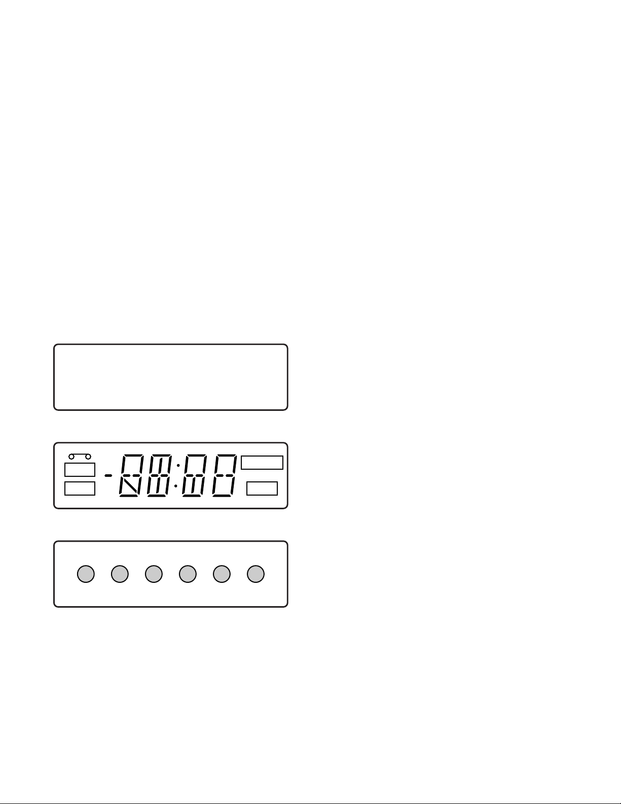
SERVICE INFORMATION FOR EEPROM IC SETTING
EEPROM option code No. setting EEPROM option code No. setting procedure
NAME HEX BINARY
OPT1 00 00000000
OPT2 00 00000000
OPT3 00 00000000
WR : OK I : EXIT MOVE :
EDIT :
MASKROM : R00
EEPROM : R00
LG CODE
MODEL NAME HEX BINARY
HR-J695EA OPTION1 10 00000000
OPTION2 61 00000000
OPTION3 44 00000000
HR-J291EA OPTION1 10 00000000
OPTION2 51 00000000
OPTION3 44 00000000
HR-J291MS OPTION1 00 00000000
OPTION2 50 00000000
OPTION3 44 00000000
HR-J297MS OPTION1 00 00000000
OPTION2 50 00000000
OPTION3 44 00000000
WR : OK I : EXIT MOVE :
EDIT :
1. DETECT NEW EEPROM (OPTION EDIT SCREEN)
- After changing EEPROM, EEPROM EDIT is displayed in the field if pressing “PLAY”key on SET
and “0” Key on Remocon in the status of powering
OFF.
For JVC model, change a remocon key by using
following JIG key.
JVC MODEL : FRONT UP + FRONT FF
(LG/JVC CODE)
Option Screen → Change JVC Code →
Service JVC R/C
- Setup option data using the cursor Up/Down key
of a remote control.
2. EEPROM WRITED COMPLETE SCREEN
- Writes data on EEPROM by using REMOCON
"OK".
- If completing the option data screen with a menu
key, Powering Off is automatically done and the
option edit screen is arranged.
3. PG ADJUST
a) Insert the PAL SP Test Tape and play.
Note) Adjust the distance of X, pressing “PLAY”
key on SET and “0” key on Remocon after
the PALSP TEST TAPE is inseted.
In Initial Mode, “- -” is displayed in CLK and
LED is ON in DOT.
b) Press again “PLAY” key on SET and “0” key on
Remocon.
(“- -” is displayed in CLK and LED is blink in DOT.
Afer adjusting PG, LED is preserved as a).)
c) Connect the CH1 of the oscilloscope to the H/SW
and CD2 to the Video out for the VCR.
d) Trigger the mixed Video Signal of CH2 to the
CH1 H/SW(W714, W715), and then check the
distance (time difference), which is from the
selected A(B) Head point of the H/SW(W714,
W715) signal to the starting point of the vertical
synchronized signal, to 6.5H ± 0.5H (416µs,
1H=30.0µs).
4. EEPROM INITIAL
- SETUP is displayed in the field if pressing the
FRONT REC KEY with the remocon number
"CLEAR" key pressed in the status of powering
Off.
- AUT O SEARCH is done since the initial screen of
ACMS is serviced if powering On.
- Check basic operation (PLAY/RECORD...)
1-6
Page 9

SPECIFICATIONS
General
Power : 100~240V, 50/60Hz
Power consumption : Approx. 12 watts(Energy Saving mode : 3 watts)
Video Head system : Rotary 2heads, helical scanning system
(HR-J291EA/HR-J291MS/HR-J297MS)
Double azimuth 4 heads, helical scanning system
(HR-J695EA)
Tape speed : 23.39 mm/sec (SP mode)11.69 mm/sec(LP mode)
Tape format : Tape width 1/2” (12.7 mm high density VHS tape)
Maximum recording time : 4 hours in SP mode/8 hours in LP mode (with E-240 tape)
Rewind time : Approx. 150 sec. (with E-180 tape)
Dimensions (W X H X D) : 360 x 94.5 x 230 mm
Weight : 9.0 lbs. (4.0 kg)
Operating temperature : 41°F-95°F (5°C-35°C)
Operating humidity : Less than 80%
Timer : 24 hours display type
Video
Input level : VIDEO IN (RCA type)
1.0 Vp-p, 75 ohm, unbalanced
Output level : VIDEO OUT (RCA type)
1.0 Vp-p, 75 ohm, unbalanced
Signal to noise ratio : More than 43 dBm
RF Modulator : UHF 28~68(Adjustable)
Audio
Input level : AUDIO IN (RCA type)
-6.0dBm, more than 47kΩ
Output level : AUDIO OUT (RCA type)
-6.0 dBm, less than 1kΩ
Track Mono track & Hi-Fi track
Frequency response : Normal : 100 Hz - 10 kHz(-6/+3 dB)
Hi-Fi : 20 Hz - 20 kHz(3-/+3 dB)
Signal to noise ratio : Normal : More than 43 dBm(at SP mode)
Dynamic range : Hi-Fi : More than 70 dBm(at SP mode)
Hi-Fi : More than 85 dBm(at SP mode)
• Design and specifications are subject to change without notice.
:HR-J695EA Model only
1-7
Page 10
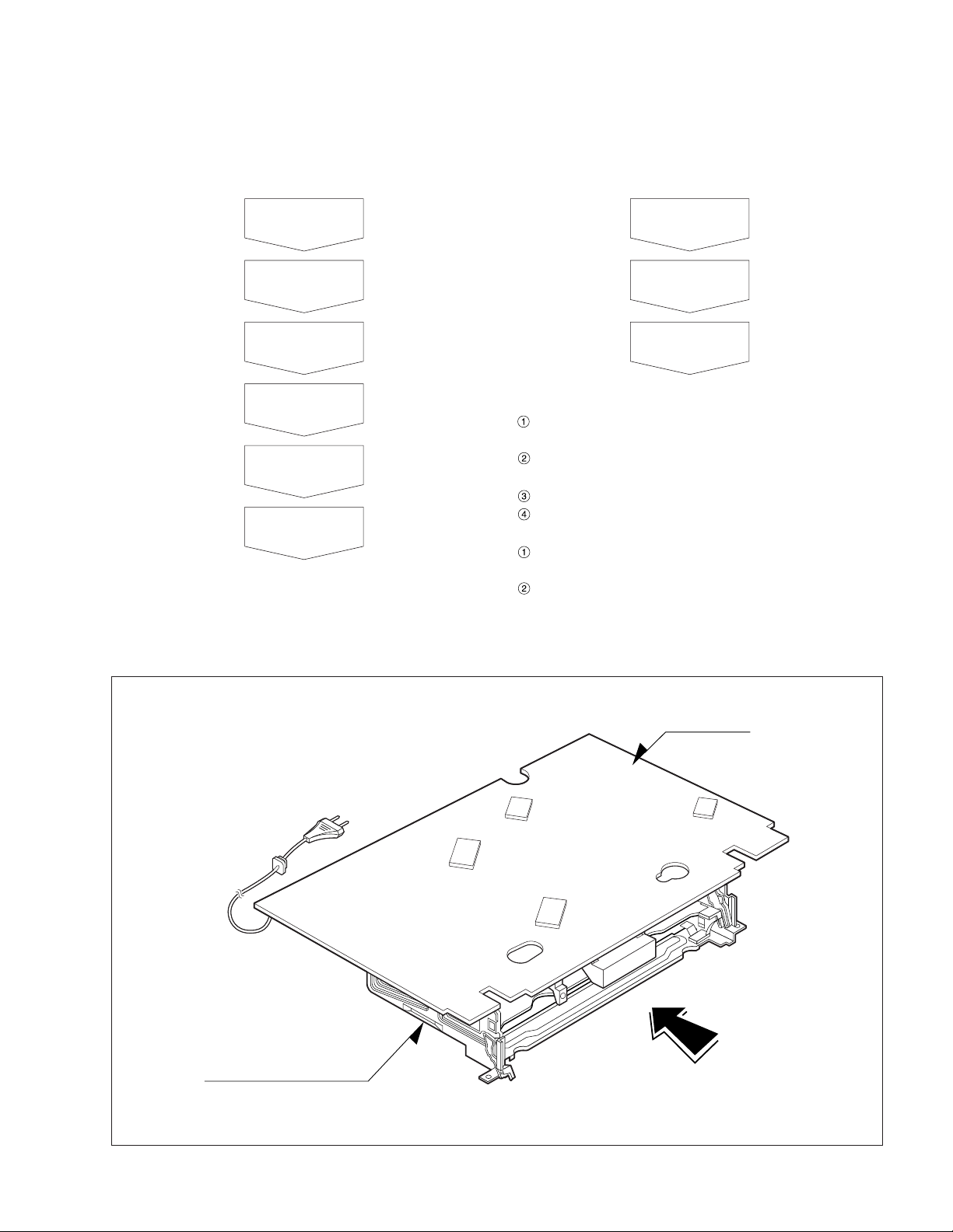
SECTION2 CABINET & MAIN FRAME
SERVICE METHOD
(1) Disassembly Flow
Bottom Cover
Housing & Deck
Top Case
Front Panel
Assembly
Main C.B.A
LED C.B.A
(2)Re-assembly Flow for service like Fig. 2-1
LED C.B.A
Main C.B.A
Housing & Deck
Assembly
(3)To check and replace Electrical parts
1 Disassemble the unit according to
No.1) Disassembly Flow.
2 Re-assemble the unit according to
No.2) Re-assembly Flow.
3 Place the unit like Fig. 2-1
4 Check and replace Electrical par ts.
NOTE :
1 Inser t Video Cassette Tape inversely like Fig. 2-1
to check and replace defective parts.
2 In disassembling and reassembling, be careful not
to damaged CST switch.
(Positioned Upside Down)
Housing y Mecanismo
C.B.A Princioal
Cassette Tape
(Upside Down)
Fig.2-1
2-1
Page 11
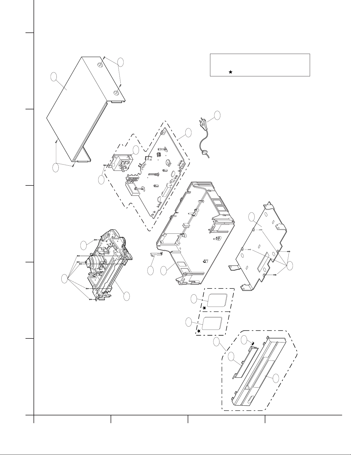
1. Cabinet and Main Frame Section
462
5
250
EXPLODED VIEWS
NOTE) Refer to “SECTION 5 REPLACEMENT
A46
PARTS LIST” in order to look for the
part number of each part.
OPTIONAL PARTS
300
4
462
457
320
330
3
464
261
260
457
2
A00
A49
452
A42
A43
1
A
BCD
284
283
280
2-2
Page 12

2.Packing Accessory Section
CABLE SET ASS'Y
806
(Optional parts)
PLUG ASS'Y 1WAY
811
(Optional parts)
NOTE) Refer to “SECTION REPLACEMENT PARTS LIST
NOTE) in order to look for the part number of each part.
OPTIONAL PARTS
810
PLUG ASS'Y 2WAY
812
(Optional parts)
INSTRUCTION MANUAL801
BATTERY808
PACKING (LF)803
BAG. SOFR SHEET804
PACKING (RF)803
BOX CARTON802
REMOCON900
2-3
Page 13

SECTION 3 ELECTRICAL
ELECTRICAL ADJUSTMENT POINTS ARRANGEMENT
: Measurement point
: Adjustment point
A/V JACK
SMPS
S
M
DECK CNT.
A/V
AVCP
Hi-Fi
TUNER &
MODULATOR
T
U
N
E
R
P
S
SYSTEM
U-COM
DOT DISP
3-1
Page 14

ELECTRICAL ADJUSTMENT PROCEDURES
1. Servo Adjustment
1) PG Adjustment
• Test Equipment
a) OSCILLOSCOPE
b) PALTEST TAPE (VHS SP)
• Adjustment And Specification
MODE
PLAY
MEASUREMENT POINT ADJUSTMENT POINT SPECIFICATION
V.Out
H/SW(W714, W715)
6.5 ± 0.5H
• Adjustment Procedure
a) Insert the PAL SP Test Tape and play.
Note) Adjust the distance of X, pressing “PLAY” key on SET and “0” key on Remocon after the PAL
SP TEST TAPE is inseted.
In Initial Mode, “- -” is displayed in CLK and LED is ON in DOT.
b) Press again “PLAY” key on SET and “0” key on Remocon.
(“- -” is displayed in CLK and LED is blink in DOT.
Afer adjusting PG, LED is preserved as a).)
c) Connect the CH1 of the oscilloscope to the H/SW and CD2 to the Video out for the VCR.
d) Trigger the mixed Video Signal of CH2 to the CH1 H/SW(W714, W715), and then check the distance
(time difference), which is from the selected A(B) Head point of the H/SW(W714, W715) signal to the
starting point of the vertical synchronized signal, to 6.5H ± 0.5H (416µs, 1H=30.0µs).
• CONNECTION
V.Out
H/SW(W714,W715)
3-2
OSCILLOSCOPE
CH1 CH2
H/SW
(W714, W715)
V.out
Page 15

ELECTRICAL ADJUSTMENT PROCEDURES
• WAVEFORM
H/SW
6.5H(416us)
Composite
VIDEO
• Attension and Reference
a) The PG checking must do when RF Level is Maximum and SERVO system is Locking (MTR MODE)
b) V.H/SW Level is 2Vpp.
3-3
Page 16

ELECTRICAL TROUBLESHOOTING GUIDE
1. Power Circuit(SMPS)
(1) No 5.3VA.
No 5.3VA.
YES
Is the F101 normal?
YES
Is the BD101 normal?
YES
Is the R101 normal?
YES
Does the oscillation wavefor m appear at
the IC101 Pin 7?
YES
NO
NO
NO
NO
Replace the F101
(Use the same Fuse).
Replace the BD101.
Replace the R101.
Is Vcc(about 13~15V) permittable at the
IC101 Pin 3?
NO
Check or Replace the D103.
Is there DC voltage at the IC101 Pin 4?
YES
Is there about 2.5V at the IC103 Vref ?
YES
Is the D106 normal?
YES
Check the Main PCB 5.3VA Line short?
NO
NO
NO
Replace the IC102.
Replace the IC103.
Replace the D106.
3-4
Page 17

7. Power Circuit(SMPS)
(2) No 12VA.(Capstan)
No 12VA.
YES
Does 5.3VA work normally? Check whether 5.3VAis out of order.
YES
Is the D109 normal?
YES
Check 12VA Line of the Main PCB short.
(3) No 12V (Hi-Fi, Buffer)
No 12VA.
YES
NO
NO
Replace the D109.
Is Vcc(about 12V) put into the Q152(E)? Replace the Peripheral Circuitry of ZD152.
YES
Is Voltage(about 13V) put into the
Q152(B)?
YES
Check or Replace the Q152.
NO
3-5
Page 18

7. Power Circuit(SMPS)
(4) No 5V
No 5V.
YES
Is 5.3VA put into the Q155(Q157)
collector?
YES
Is the Q156 Base “H”?
YES
Is about 4.7V put into the
Q155(Q157) Base?
YES
Check or Replace the Q155(Q157).
NO
NO
Check the µ-com Control.
Check the Q156
whether it works normally.
3-6
Page 19

2. Servo Circuit
A.
Unstable Video in PB
Mode.
Does the on screen noise
level change periodically?
YES
Do CTL pulses appear at
IC501 pin 97?
YES
Does the CFG divide
wavefor m appear at IC501
pin 87?
YES
Do the CTL pulses move
when TRK is operated?
YES
NO
Is the height of the CTL
Head adjusted correctly?
NO
Adjust the CTL Head.
NO
Does the Video Envelope
wavefor m appear at IC501
Pin 9?
YES
Replace IC501.
Replace IC501.
NO
Check Y/C Block.
3-7
Page 20

B.
Drum Motor stopped.
Does 12V appear at PMC01 PIN8?
YES
Does Drum CTL signal appear at PMC01
PIN12?
Check Connector and Drum Motor Ass’y.
YES
Check the Components and foil Pattern
between IC501 Pin 76 and PMC01
Pin 12 for shorts.
YES
Do DPG/FG Pulses appear at IC501
Pin 90?
YES
Does the Drum PWM wavefor m
appear at IC501 Pin 76?
YES
NO
Check Power.
NO
Does Drum PWM appear at IC501
Pin 76?
NO
Do DPG/FG Pulses appear at PMC01
Pin 11?
NO
Check Drum Monitor Ass’y.
NO
Check the Components and foil pattern
between PMC01 Pin 11 and IC501
Pin 90 for shorts.
NO
Check the Components and foil Pattern
Connected to IC501 Pin 76 PMC01
Pin 12 for shorts.
Replace IC501.
3-8
Page 21

C.
Capstan Motor Stopped.
Does 12VA appear at PMC01 Pin 2?
YES
Does 2.8V appear at PMC01 Pin 9?
YES
Check Connector and Capstan
Motor Ass’y .
YES
Check the Components and foil Patterns
Connected between IC501 Pin 77 and
PMC01 Pin 9 for shorts.
YES
Does the CFG signal appear at IC501
Pin 87?
YES
Does Capstan PWM appear at IC501
Pin 77?
YES
NO
Check Power.
NO
Does PWM wave appear at IC501
Pin 77?
NO
Does the CFG signal appear at PMC01
Pin 1?
NO
Check Capstan Motor Ass’y.
NO
Check Components and foil patter ns
between PMC01 Pin 1 and IC501
Pin 87 for shorts.
NO
Check the components and foil pattern
connected between IC501 Pin 77 and
PMC01 Pin 9 for shorts
Replace IC501.
3-9
Page 22

3. System & Front Panel Circuit
A.
Auto stop.
Does SW30 wavefor m
appear at IC501 Pin 18?
YES
NO
Do Take-up reel pulses
appear at IC501 Pin 80?
YES
Change IC501.
NO
Check the Drum Motor
Signal.
Does 5.3V appear at
RS501.
YES
Replace the Take-Up Reel
Photocoupler on Main
PWB Board(RS501).
NO
Check the Power.
3-10
Page 23

B.
Cassette tape loading is unstable.
Is REG 12V applied to PMC01 Pin 8?
YES
Is High signal applied to IC501 Pin 58
When inserting the CST?
YES
Does Low signal occur form IC501 Pin 60
when inserting the CST?
YES
Check the Deck Mechanism.
NO
NO
NO
Check the power.
Is 5.3V applied to R544?
YES
Check the CST SW and
peripheral circuitry.
Check IC501 Pins 22, 23, 24, 25.
Change IC501.
NO
Check the power.
YES
NOTE : Auto stop may also be caused by lack of lubrication,due to dried grease or oil.
3-11
Page 24

C.
Non working functon buttons.
Is the voltage of IC501 Pin 99, 5V?
D.
YES
Does LED CLOCK, LED DOT display
change when a function button is
pressed?
YES
Replace IC501.
LED CLOCK, LED DOT doesn’t work.
Is 5V applied to IC501 Pins 37 and
IC5F1 Pins 5, 18?
YES
Check the ( OPTION 1)
NO
Check the power.
NO
Replace the defective Switch.
(Function SW)
NO
Check the power circuit.
YES
Do pulse appear at IC501 Pins 65, 66
and 67.
YES
Do oscillation appear at IC5F1 Pin1.
YES
Check the foil patterns between IV5F1
and OPTION2.
YES
Replace OPTION 2
NO
Replace IC501.
NO
Replace IC5F1.
OPTION 1 : D5E4 LED CLOCK
OPTION 2 : LED 501 - LED CLOCK
LED 502 - LED DOT
3-12
Page 25

4. Y/C CIRCUIT
(1) No Video in EE Mode,
No Video in EE Mode
Does the Video signal
appear at the IC301 Pin 48?
YES
Is 5V applied to the IC301
Pins 18, 24, 42, 55, 72, 91?
YES
Does the Video signal
appear at the IC301 Pin 65?
YES
Does the Video signal
appear at the IC501 Pin 50?
YES
Does the Video signal
appear at the Emitter terminal of the Q701?
NO
NO
NO
NO
NO
Check the Video Input
Jack.
(Line In Jack)
Check the 5.2V, 5.4VA
Line. (Power Circuit)
Is I2C BUS signal applied to
the IC301 Pins 68, 69?
YES
Chck the path of the signal
between the IC301 Pin 5
and IC501 Pin 50.
Does the 12V appear at
the Emitter terminal of the
Q701.
NO
NO
Check the System Circuit.
(Refer to ‘SYSTEM I2C BUS
CHECK Trouble Shooting’)
Check C316. (AGC)
YES
Replace the IC301.
YES
Replace the Q701.
3-13
Check the 12V Line.
(Power Circuit)
Page 26

3. Y/C CIRCUIT
(2) When the Y(Luminance) signal doesn’t appear on the screen in PB Mode,
Is 5.2VT, 5.4VAapplied to the
IC301 Pins 24, 42, 55, 72, 91?
YES
Is the I2C Bus siganl applied
to the IC301 Pins 68, 69 ?
YES
Does the normal RF signal
appear at the IC301 Pin 78?
YES
NO
NO
NO
Check the line of the 5.2V
Line. (Power Circuit)
Refer to ‘SYSTEM I2C BUS
CHECK Trouble Shooting’.
Is the V.H.S/W signal
applied to the IC301 Pin 70?
YES
Is V.H.S/W “H” about 3.4V
at the IC301 Pin 70?
YES
Clean the Drum.
NO
NO
NO
Check the System Circuit.
(IC501 Pin 18)
Check the V.H.S/W level.
(Check R303, R304)
Replace the IC301.
Does the Y(Luminance) RF
signal appear at the IC301
Pin 76?
YES
Is the Y(Luminance) Video
wavefor m showed up at
theIC301 Pin 43?
YES
Replace the IC301.
NO
NO
Check the path of the
Y(Luminance) RF signal.
(Check the C312)
Check the path of the
Y(Luminance) RF signal.
(Check C327)
YES
YES
3-14
Page 27

3. Y/C CIRCUIT
(3) When the C(Color) signal doesn’t appear on the screen in PB Mode,
Is 5.2V/5.3VA applied to the
IC301 Pins 24, 42, 55, 72, 91.
YES
Is the Color Rotary signal
applied to the IC301
Pin 70?
YES
Is Color Rotary “H”
about 3.4V?
YES
Does the Color signal
appear at the IC301
Pin 25 ?
YES
NO
NO
NO
NO
Check the line of the 5.2V/
5.3VA Line. (Power Circuit)
Check the Color Rotary
Circuit. (IC501 pin 15)
Check the Color Rotary
level. (Check the R303)
Does the X301(4.43MHZ)
oscillate?
Does the Color signal
appear at the IC301 Pin 21?
NO
NO
Replace the X301.
Check the Color Pass.
Replace the IC301.
YES
Replace the IC301.
3-15
Page 28

3. Y/C CIRCUIT
(4) When the Video signal doesn’t appear on the screen in REC Mode,
Is the EE signal normal?
YES
Is 5.2V/5.3VA applied to the
IC301 Pins 24,42,55,72,91?
YES
Does PB Mdoe operate
normally?
YES
Does the RF signal appear
at the IC301 Pin 78?
YES
NO
NO
NO
NO
Check EE Mode.
Check the line of the 5.2V/
5.3VA Line.(Power Circuit)
Check PB Mode.
Is the REC ‘H’ signal
(about 4V) applied to the
IC301 Pin 80?
YES
Check REC Luminance
Pass & Color Pass.
NO
YES
Check the System of REC
‘H’. (the IC501 Pin 74
/ the D301)
Replace the IC301.
Does the REC RF signal
appear at the IC301
Pins 88,89,94,95?
YES
Check the Drum &
Drum Connector
NO
Check the circuit of the
IC301 Pins 85, 86.
YES
3-16
Page 29

5. Tuner/IF circuit
(1) No picture on the TV screen
No picture on the
TV screen
YES
Does the Video signal at
the TU701 Pin24?
YES
NO
Is +30V applied to
TU701 Pin 16?
YES
Is +5.2V applied to
TU701 Pin 13?
YES
Does the Clock signal
appear at TU701 Pin 11?
YES
Does the data signal
appear at TU701 Pin 12?
YES
Replace Tuner
NO
NO
NO
NO
Check 34V line.
Check 5.2V line.
Check the liC Clock
signal of µ-com Pin 71.
Check the liC Data signal
of µ-com Pin 72.
Does the Video signal at
the IC501 Pin50?
YES
Check the signal flow from
IC501 Pin52 to JK301.
NO
Check the signal flow
from TU701 Pin 24 to
IC301 Pin 48.
3-17
Page 30

(2) No sound (Mono Model)
No sound
YES
Check the Vcc of IC301 Pin 18.
YES
Check the Tuner Audio signal
at IC301 Pin 13.
YES
Check the Audio signal at IC301 Pin 11.
YES
Check the signal flow from IC301
pin 11 to JK301.
NO
NO
NO
Check 5.2V power.
Chekc the signal flow from TU701
Pin21 to IC301 Pin 13.
Replace IC301.
3-18
Page 31

(3) No sound (Hi-Fi Model)
No sound
YES
Check the Vcc of IC751 Pins 1, 19, 33.
YES
Check the Tuner SiF signal at IC751 Pin 2.
YES
Check the oscillator of IC751 Pins 5, 6.
YES
Check the Audio of IC751 Pins 30, 31.
YES
Check the Audio of IC801 Pins 2, 3.
YES
NO
NO
NO
NO
NO
Check 5V power.
Check the Tuner Audio of TU701 Pin 21.
Replace X751.
Check the IIC Clock and Data at
IC751 Pins 12, 13.
Check the signal flow from IC751
Pins 30, 31 to IC801 Pins 2,3.
Check the Audio of IC801 Pins 18, 19.
YES
Check the signal flow from IC801
pins 18, 19 to JK301.
NO
3-19
Check the IIC Clock and Data at
IC801 Pins 42, 43.
Page 32

6. Hi-Fi Circuit (Hi-Fi Model)
A.
Hi-Fi Playback.
No sound
Check the Hi-Fi Selection
Switch and the Tape quality.
YES
Is the RF Envelope at
IC801 Pin 44 over 2Vp-p?
YES
Check IC801 Pin 42(Data),
Pin 43(Clock).
YES
Do Audio signals appear at
IC801 Pin 16(L-CH),
17(R-CH)?
YES
NO
NO
YES
NO
Check the Vcc of
IC801.(Pins 34, 40)
YES
Is the Head switching signal
IC802 Pin 41 O.K?
YES
Check the connection at
P3D01 if good then
Replace IC801.
Check Ports of µ-COM.
NO
NO
Check power.
Check IC501 Pin 19.
(Audio head switch 25)
Check the Signal path
of Audio Output.
Replace IC801.
3-20
Page 33

B.
Hi-Fi REC.
It is impossible to record and playback
Hi-Fi Audio signal.
YES
Check Vcc of IC801. (Pins 34,40)
YES
Check IC801 Pin 42(Data),Pin 43(CLOCK).
YES
Do Audio signals appear at IC801
Pins 16, 17?
YES
Do FM Audio signals appear at IC801
Pin 36?
YES
Check the Contact Points of Drum
Connector if good then Replace the Drum.
NO
Check Power.
NO
Check ports of µ-COM.
NO
Check Audio input signal of IC801
Pins 2, 3(TU.A.), 6, 7(Scart 1)
NO
Replace IC801.
3-21
Page 34

VICTOR COMPANY OF JAPAN, LIMITED
12,3-chome,Moriya-cho,Kanagawa-ku,Yokohama,Kanagawa-prefecture,221-8528,JapanHOME AV NETWORK BUSINESS UNIT.
Printed in Japan
0208 VP
 Loading...