Page 1

SERVICE MANUAL
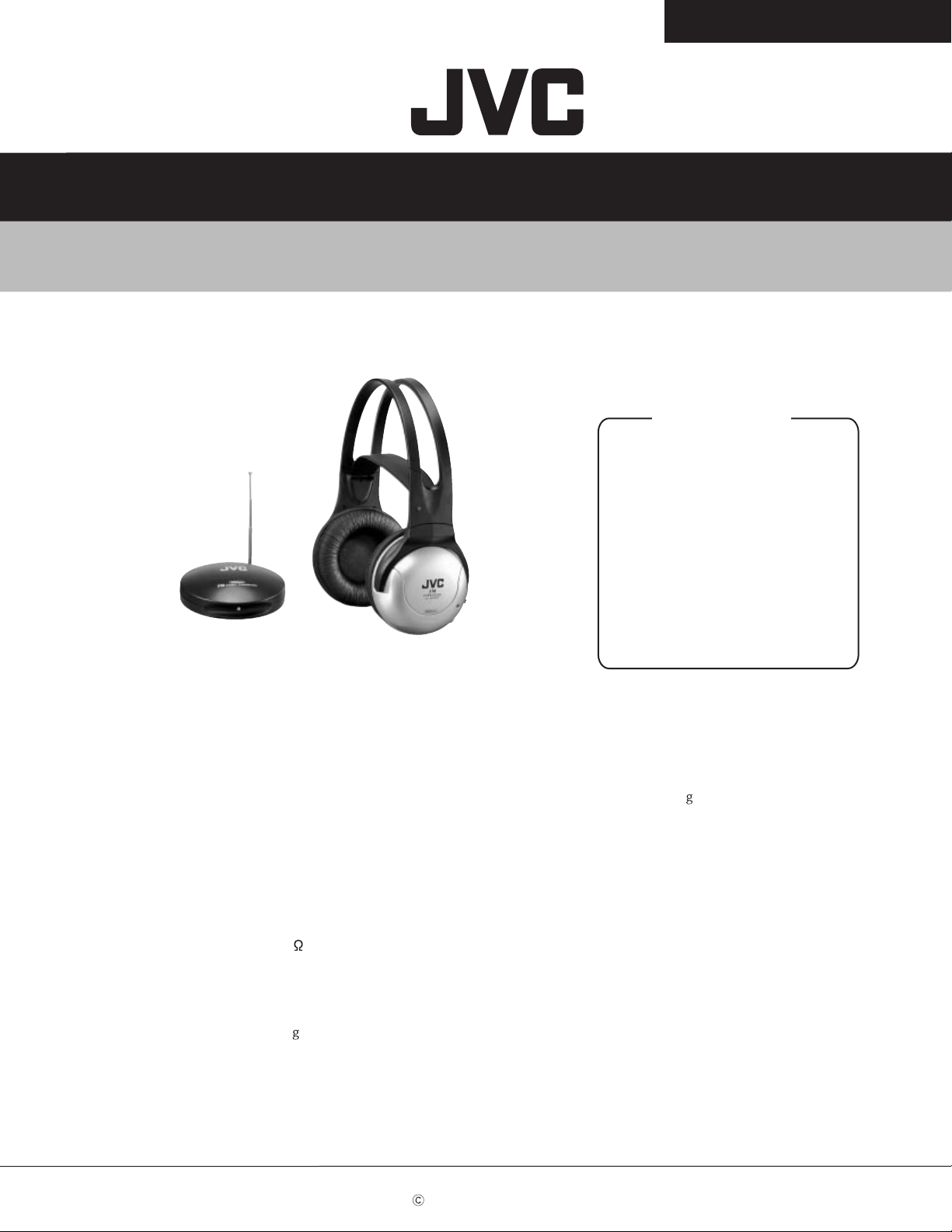
CORDLESS FM STEREO HEADPHONES
HA-W500RF (EG)/(EK)
Specifications
HA-W500RF (EG)/(EK)
Contents
Specifications ------------ Front cover
1. Disassembly ------------------------- 3
2. Schematic Diagram ---------------- 4
3. Measurement Condition --------- 5
4. Print Circuit Board ----------------- 5
5. Wiring Diagram --------------------- 7
6. Block View Inside IC -------------- 7
7. Block Diagram ---------------------- 8
8. Electric Parts List ------------------ 8
9. Exploded view ----------------------- 9
10 .Mechanical Parts List ------------ 9
11. Packing Method ------------------ 10
12. Packing Materials Parts List - 10
13. Accessories List ----------------- 10
General Specifications
System : Radio Frequency (UHF stereo)
Modulation : Frequency modulation
Carrier frequency : 863-865 MHz
Usable area
(distance to reach) : Approx. 100m (328 ft) : using
JVC measurements systems
Frequency response : 30 Hz-15,000 Hz
Distortion : Less than 4 % (at 1 kHz)
Transmitter (J22121-001)
Power requirements : DC 9 V (with the exclusive AC
adaptor J47126-001(EG Model)
/J47127-001(EK Model))
Audio input ter minal : 3.5 mm dia. stereo mini plug
Input impedance : 25 k
Reference input level : 300 mV
Dimensions : 100(W) x 100(D) x 106(H) mm
(3-15/16" x 3-15/16" x 4-3/16")
(Including antenna)
: 115
Mass
(4.1 oz)
(Without connection cord and AC
adaptor)
Headphones (HA-W500RF)
Power requirements : Rechargeable
Ni-Cd batter y (1.2 V) x 2
Battery running time : 20 hours
(When charged for 24 hours)
Mass : 280
Provided Accessories
Instructions x 1
AC adaptor x 1
Connection cord x 1 (3.5 mm dia. stereo mini jack-
Plug adaptor x 1 (converts 3.5 mm dia. stereo
(9.9 oz)
(With installed rechargeable
Ni-Cd batter y x 2)
RCA pin plug x 2 : 0.1 m (0.3 ft))
mini plug to a 6.3 mm dia. standar d
stereo phone plug)
* Design and specifications subject to change without notice.
COPYRIGHT 2002 VICTOR COMPANY OF JAPAN, LTD.
No.70270
Sep. 2002
Page 2

HA-W500RF (EG)/(EK)
Safety Precautions
1. This design of this product contains special hardware and many circuits and components specially
for safety purposes. For continued protection, no changes should be made to the original design
unless authorized in writing by the manufacturer. Replacement parts must be identical to those
used in the original circuits. Services should be performed by qualified personnel only.
2. Alterations of the design or circuitry of the product should not be made. Any design alterations of
the product should not be made. Any design alterations or additions will void the manufacturer`s
warranty and will further relieve the manufacture of responsibility for personal injury or property
damage resulting therefrom.
3. Many electrical and mechanical parts in the products have special safety-related characteristics.
These characteristics are often not evident from visual inspection nor can the protection afforded
by them necessarily be obtained by using replacement components rated for higher voltage,
wattage, etc. Replacement parts which have these special safety characteristics are identified in
the Parts List of Service Manual. Electrical components having such features are identified by
shading on the schematics and by ( ) on the Parts List in the Service Manual. The use of a
substitute replacement which does not have the same safety characteristics as the recommended
replacement parts shown in the Parts List of Service Manual may create shock, fire, or other
hazards.
4. The leads in the products are routed and dressed with ties, clamps, tubings, barriers and the
like to be separated from live parts, high temperature parts, moving parts and/or sharp edges
for the prevention of electric shock and fire hazard. When service is required, the original lead
routing and dress should be observed, and it should be confirmed that they have been returned
to normal, after re-assembling.
5. Leakage currnet check (Electrical shock hazard testing)
After re-assembling the product, always perform an isolation check on the exposed metal parts
of the product (antenna terminals, knobs, metal cabinet, screw heads, headphone jack, control
shafts, etc.) to be sure the product is safe to operate without danger of electrical shock.
Do not use a line isolation transformer during this check.
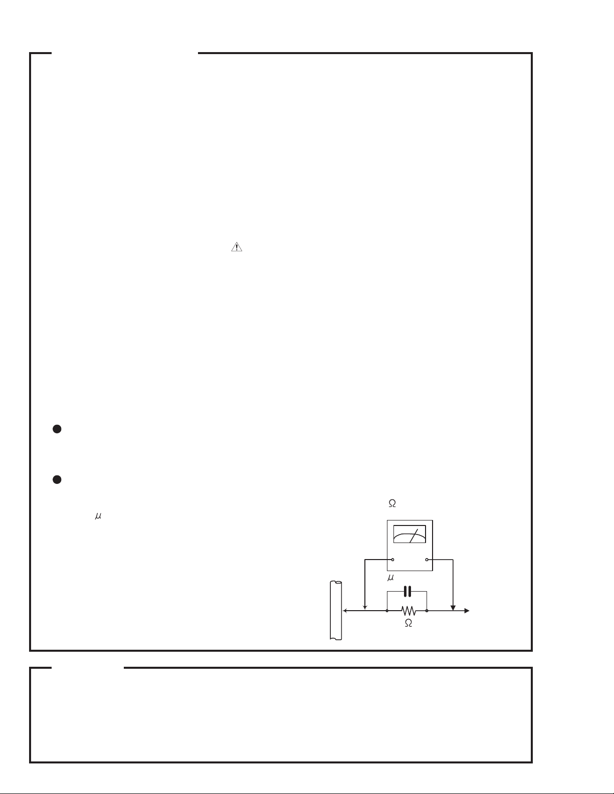
Plug the AC line cord directly into the AC outlet. Using a "Leakage Current Tester", measure
the leakage current from each exposed metal parts of the cabinet , particularly any exposed
metal part having a return path to the chassis, to a known good earth ground. Any leakage
current must not exceed 0.5mA AC (r.m.s.)
Alternate check method
Plug the AC line cord directly into the AC outlet. Use an AC voltmeter having, 1,000 ohms
per volt or more sensitivity in the following manner. Connect a 1,500 10W resistor paralleled by
a 0.15 F AC-type capacitor between an exposed
metal part and a known good earth ground.
Measure the AC voltage across the resistor with the
AC voltmeter.
Move the resistor connection to eachexposed metal
part, particularly any exposed metal part having a
return path to the chassis, and meausre the AC
voltage across the resistor. Now, reverse the plug in
the AC outlet and repeat each measurement. voltage
measured Any must not exceed 0.75 V AC (r.m.s.).
This corresponds to 0.5 mA AC (r.m.s.).
0.15 F AC TYPE
1500 10W
Good earth ground
AC VOLTMETER
(Having 1000
ohms/volts,
or more sensitivity)
Place this
probe on
each exposed
metal part.
Warning
1. This equipment has been designed and manufactured to meet international safety standards.
2. It is the legal responsibility of the repairer to ensure that these safety standards are maintained.
3. Repairs must be made in accordance with the relevant safety standards.
4. It is essential that safety critical components are replaced by approved parts.
5. If mains voltage selector is provided, check setting for local voltage.
2 (No.70270)
Page 3

1.Disassembly
Transmitter
In case of some problems arise in this transmitter unit,
have to change the transmitter unit itself, due to avoid
the law of radio regulation.
Receiver(Headphones)
HA-W500RF (EG)/(EK)
L
10
9
11
12
2
8
7
6
1
5
4
4
15
R
4
1
4
3
13
R
14
R
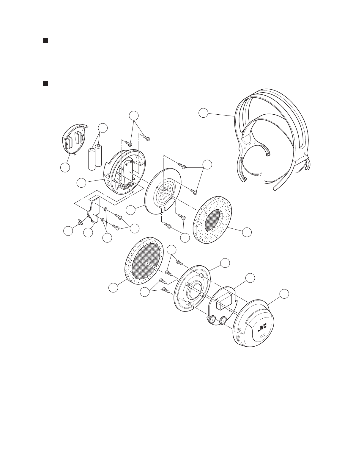
1.Remove the ear pad 1 from the driver unit ass'y (L) 2 and (R) 3.
2.Remove the screw 4 and pull up the driver unit ass'y (L) 2 and (R) 3.
3.At channel L. Remove the screw 5 and insulation washer 6, and pull up the charge print circuit board 7.
4.Remove the switch knob 8.
5.Remove the screw 9 and remove the battery door 10 from the housing ass'y (L) 12.
6.Remove the battery 11 from the housing ass'y (L) 12.
7.At channel R. Remove the main print circuit board 13 from the housing (R) 14
8.Remove the wire with solder from the charge and main print circuit board 7 13, then remove the headband
ass'y 15.
(No.70270) 3
Page 4

HA-W500RF (EG)/(EK)
g
2.Schematic diagram
ANT1
C75
1
Test-1
L3
12nH
IC1 7201-15
3 1
VI VO
GND
2
C1
3p*
X1 C2
D1
V809
Test-10
JX1
CHARGE OUTPUT
TERMINAL
C39
1000p
C48
1000p
!
X4
863MHz
R30
1k
C8
100p
TC1
1.5-3p
C3
5p6
R24
R2
1K
39k
VR4
5k
!
S1a SW SPDT
R50
330
0.01u
L2
C881000p
15nH
C76
9
0
VR2
100k
C5
1u
C52
0.01u
C51
22P
4
R49
27K
C47
1000p
C59
10u
C17
3P*
C46
0.1u
C20
2P(N)
Q9
5508
100p
R28
1k
R27
1k
VR3
5k
R42
50
R40
1M
C78
1p
R29
100
K
L1
15nH
R1
18k
Q1
50
R4
3P*
47
R25
1k
R26
1k
C80
0.01u
R53
27K
C77
1p
R56
0
C45
0.1u
VR3 795.1Mhz
VR4 791.5Mhz
+
BATTERY
-
!
82K
R46
R41
C73
0.1u
75k
Test-11
R54
330
C874p
C81
0.01U
Q11
5508
2.4V
3
2
+
S1bSW SPDT
C44
10u
!
84
+
-
L9
15nH
C83
10p
*
N750
ON
OFF
R37300
R38
100k
IC4A
LM393 or
NJM2903M
1
R39
68k
C41
C19
1u
0.001u
C84
0.01u
Q8
R35
100k
R36
100k
R18
10
R13
1k5
IC4B
84
LM393 or
5
NJM2903M
+
6
-
7
R47 18k
3904
D2A RED
D2B GREEN
D3 4148 Q68550
C60
47u
X3
10.7M
IC5
78L06
L8
0.33uh
R11
100
GND
2
R434k7
Q7
3904
C53
56P
X2
10.7MHz
31
VIVO
C61
10u
Test-3
R12
330
4148
R4510k
R4410k
C21
12p
C49
10
Test-6
Test-7
C22
12
7p
+
R14
100K
15 29
813 9
C30
0.01U
R16
3k3
11
C31
10U
T2
p
C25
+
+
C24
C23
10U
0.1U
Test-1 High RF in
C72
4U7
2
35
6
+
+
Test-3 Low RF in
Test-5 R out
Test-6 L out
Test-7 GND
Test-8 VCC
Test-9 STEREO
Test-10 VT
TEST-11 REF V
VR1b
100k
C38
C36
100u
+
2U2
R19
2k7
R20
2k7
VR1a
100k
+
C37
2U2
4U7
3020
17
Test-9
1
27
R34
2k2
C32
+
0.47u
R33
+
2
2K
R22
27k
R21
100K
1
7
C33
4U7
OUT1
OUT2
8
BY PASSMUTE
4
Rout
Lout
IC3
LM4809
VCC
IN1
IN2
GND
R32
3K3
C54
2u2
+
+
C55
2u2
C73
220u
(C74)
C32
220u
R23
27k
VR5
5K
+
+
T1
C40
1u
C10
10p
21 4
18
26
722
IC2
CXA1538M
216 28
6233
5
25
+
C27
1U
R31
2K2
R15
3k3
D4
C34
0.015u
+
C26
1U
Test-8
C43
220u
+
+
+
C28
C29
4U7
33U
C35
0.015u
Test-5
C42
0.1u
SPK1
32ohm
Rout
SPK2
32ohm
Lout
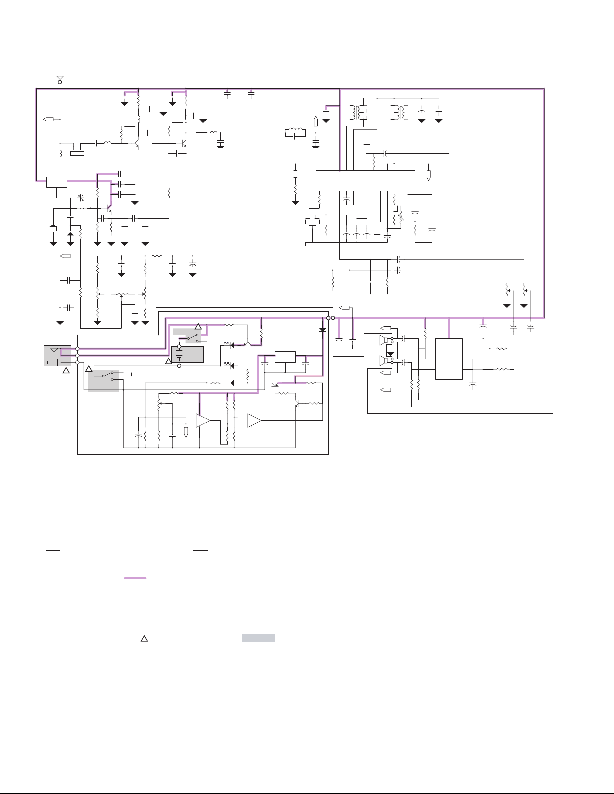
Use of Circuit Diagram
Notes:
1. The thick line ( ) is the B (+) power supply.
2. This circuit diagram is the r eference diagram. Cir cuits and constans ar e subject to change without notice for
improvement.
3. Values printed in r ed show the voltares of each section measur ed by the tester (inter nal resistance 20 kOhms/V),
with the power switch ON.
4. Parts marked with (in the shaded area ) are safety parts.When replacing these, be sure to use only the
nated parts to ensure safety.
desi
4 (No.70270)
!
Page 5

3.Measurement Condition
HA-W500RF (EG)/(EK)
AC IN
Transmitter Receiver (Headphones)
4.Print Circuit Board
Receiver (Headphones)
CHARGE P. C. BOARD
Reference input signal :1kHz 300mVp-p sine wave
Hedaphone volume control : MAX
Distance : 1m (3.28ft)
shows the B(+) power supply
shows the ground
shows others.
Surface
TOP
Back side
(No.70270) 5
Page 6

HA-W500RF (EG)/(EK)
4.Print Circuit Board
Receiver (Headphones)
MAIN P.C.BOARD
TOP
Surface
shows the B(+) power supply
shows the ground
shows others.
D
C
B
A
1234
Back side
Receiver (Headphones)
MAIN P.C.B. LOCATION
Symbol
ICs
IC2
IC3
IC4
IC5
Transistors
Q6
Q7
Q8
Filters
X2
X3
Diodes
D2
D3
D4
Resistors
R1
R2
R3
R4
R5
R6
R7
R8
R9
R10
6 (No.70270)
Location
2B
2A
CHG.PCB
CHG.PCB
CHG.PCB
CHG.PCB
CHG.PCB
3C
2B
CHG.PCB
CHG.PCB
CHG.PCB
Symbol
R11
R12
R13
R14
R15
R16
R17
R18
R19
R20
R21
R22
R23
R24
R25
R26
R27
R28
R29
R30
R31
R32
R33
R34
R35
R36
Location
Resistors Resistors
1B
CHG.PCB
2B
3B
3B
CHG.PCB
2A
2A
2A
3A
2A
3D
4C
4C
4C
4C
3D
3C
2B
2B
2B
CHG.PCB
CHG.PCB
Symbol
R37
R38
R39
R40
R41
R42
R43
R44
R45
R46
R47
R48
R49
R50
VR1
VR2
VR3
VR4
VR5
JP1
JP2
JP3
JP4
Capacitors
C21
C22
Location
CHG.PCB
CHG.PCB
CHG.PCB
CHG.PCB
CHG.PCB
CHG.PCB
CHG.PCB
CHG.PCB
CHG.PCB
CHG.PCB
CHG.PCB
3A
4B
4C
4C
1B
1C
3D
3D
1B
2C
Symbol
C23
C24
C25
C26
C27
C28
C29
C30
C31
C32
C33
C34
C35
C36
C37
C38
C39
C40
C41
C42
C43
C44
C45
C46
C47
C48
Location
Capacitors Capacitors
1C
1C
1B
3B
3B
2B
3B
3C
1B
2B
3B
3B
3B
3A
3A
2A
3D
2D
2D
4D
4C
3C
4B
3D
Symbol
C49
C50
C51
C52
C53
C54
C55
C59
C60
C61
C72
C73
C74
T1
T2
L8
Location
2B
2C
3B
3A
CHG.PCB
CHG.PCB
CHG.PCB
2A
3A
2A
Coils
1B
2C
2C
Page 7

5.Wiring Diagram
Inside of the housing (R)
Antenna
Black
lead
Inside of the
head band
ass'y
HA-W500RF (EG)/(EK)
Inside of the housing (L)
Red lead
Ni-Cd
Battery
Black lead
Speaker
Red lead
(Rch)
Blue lead
6.Block View Inside IC
PLL LPF1
PILOT DET LPF2
PILOT DET LPF2
ST IND/VCO CHECK
Rch OUT
Lch OUT
Vcc
RIPPLE FILTER
AGC AFC 1
AGC AFC 2
GND
TUNE IND
FM IF IN
AM IF IN
BAND SELECT
1
2
3
4
5
6
7
8
9
10
11
12
13
14
15
RX:IC2
CXA1538M
GND
30
PLL LPF2
29
MPX REG
28
VCO
27
FM DISCRI
26
MUTE
25
AM OSC
24
AFC
23
FM OSC
22
REG
21
FM RF
20
AM RF IN
19
FM RF IN
18
FE GND
17
FM/AM FE OUT
16
Natural shielded lead
Red shielded lead
Green shielded lead
Natural shielded lead
Output 1
Input 1
Bypass
Output 1
-Input 1
+Input 1
Inside of the
head band ass'y
1
2
3
4
GND
LM4809
1
2
3
4
GND
NJM2903M
RX:IC3
RX:IC4
LM393
Green
shielded lead
Natural shielded lead
8
Vcc
7
Output 2
6
Input 2
5
Shutdown
8
Vcc
7
Output 2
6
-Input 2
5
+Input 2
Speaker
(Lch)
(No.70270) 7
Page 8

HA-W500RF (EG)/(EK)
7.Block Diagram
Receiver (Headphones)
ANT
TUNING
VT
UHF
Ni-Cd Battery
(1.2V) x 2
ANT
POWER
SW1
MODULE
ON
OFF
ON
OFF
IF
VB
FILTER
POWER INDICATOR
LED RED
VR2
COMPARATOR
IC4:LM393
NJM2903
-
22 20
OSC RF
5
Rch
18
RF IN
7
FM STEREO RADIO
IC2:CXA1538M
13
16
CHARGE INDICATOR
LED GREEN
AF OUT
6
Lch
AF OUT
DISCRIFE OUTIF INVcc
26
CHARGE INPUT
VOLUME
VR1
2
HEADPHONE
6
IC3:LM4809
AMP
8
1
Rch OUT
7
Lch OUT
4
8.Electric Parts List
Transmitter
A Item No. Parts No. Parts Name Description
A
In case of some problem arise in this transmitter unit, have to change the transmitter unit
itself, due to avoid the law of radio regulation.
Parts marked (A ) ave safety parts. When replacing, be sure to use the specified one.
Receiver (Headphones)
A Item No. Parts No. Parts Name Description
A J22133-001 Main P.C.B Ass'y Adjusted
J22134-001 Charge P.C.B Ass'y
D2 J47138-001 LED Power and charge Indicator
VR1 J47139-001 Variable Resistor Volume control, 100 k X 2
VR2 J47140-001 Variable Resistor Tuning control, 100 k X 1
A SW1 J47145-001 Power Switch Slide
A JK1 J47141-001 Charge Jack
Parts marked (A ) are safety parts. When replacing, be sure to use the specified one.
J22121-001 Transmitter Unit
8 (No.70270)
Page 9

9.Exploded View
Receiver(Headphones)
HA-W500RF (EG)/(EK)
L
4
2
7
Charge P.C.B. Ass'y
11
9
10
5
11
10
10
8
10
R
1
R
8
6
Main P.C.B. Ass'y
3
10.Mechanical Parts List
Receiver(Headphones)
A Item No. Parts No. Parts Name Q'ty Description
1 J34073-001 Headband Ass'y 1 with connecting wir e
2 J34074-001 Housing(L) Ass'y 1 with battery terminal
3 J34075-001 Housing(R) Ass'y 1
4 J34076-001 Battery Door 1
5 J34077-001 Driver Unit(L) Ass'y 1
6 J34078-001 Driver Unit(R) Ass'y 1
7 J47146-001 Swihch knob 1
8 J47144-001 Ear Pad 2
9 J46514-001
10 QYSPSPU1411M Screw 8
11 QYSPSFT1403M Screw 4
Parts marked ( A ) are safety parts. When replacing, be sur e to use the specifide one.
Rechargeable Ni-Cd batteries
1
R
with protector
with protector
2pcs/pack
(No.70270) 9
Page 10

HA-W500RF (EG)/(EK)
11.Packing Method
8
1
4
3
5
10
12
2
9
7
6
12.Packing Materials Parts List
A Item No. Parts No. Parts Name Q'ty Description
1 J22110-001 Packing case 1 for (EG) model
1 J22110-002 Packing case 1 for (EK) model
2 J22135-001 Packing Holder 1
3 J47142-001 Sub Packing Holder 1
4 QPA01202005 Poly Bag 1 for transmitter
5 QPA01506005 Poly Bag 1 for receiver(headphones)
6 QPA00500805 Poly Bag 1 for connection cord
7 QPA01202005 Poly Bag 1 for AC Adaptor
Parts marked ( A ) are safety parts. When replacing, be sur e to use the specifide one.
13.Accessories List
A Item No. Parts No. Parts Name Q'ty Description
A 8 J5500-114A Instructions 1 for (EG) model
A 8 J5500-115A Instructions 1 for (EK) model
9 BT-54008-4
A 10 J47126-001 AC Adaptor 1 for (EG) model
A 10 J47127-001 AC Adaptor 1 for (EK) model
11 J47143-001 Connection cor d 1
12 J46517-001 Plug adaptor 1
European Guarantee Certificate
11
1
Parts marked ( A ) are safety parts. When replacing, be sur e to use the specifide one.
10 (No.70270)
Page 11

< MEMO >
HA-W500RF (EG)/(EK)
(No.70270) 11
Page 12

HA-W500RF (EG)/(EK)
VICTOR COMPANY OF JAPAN, LIMITED
COMMUNICATION NETWORK BUSINESS UNIT
AV & MULTIMEDIA COMPANY 1644, Shimotsuruma, Yamato, Kanagawa 242-8514, Japan
No.70270
Printed in Japan
200209
 Loading...