

Page 1

SECTION 8
DESCRIPTION OF NEW CIRCUITRY
8.1 OUTLINE OF DV
8.1.1 Features of DV
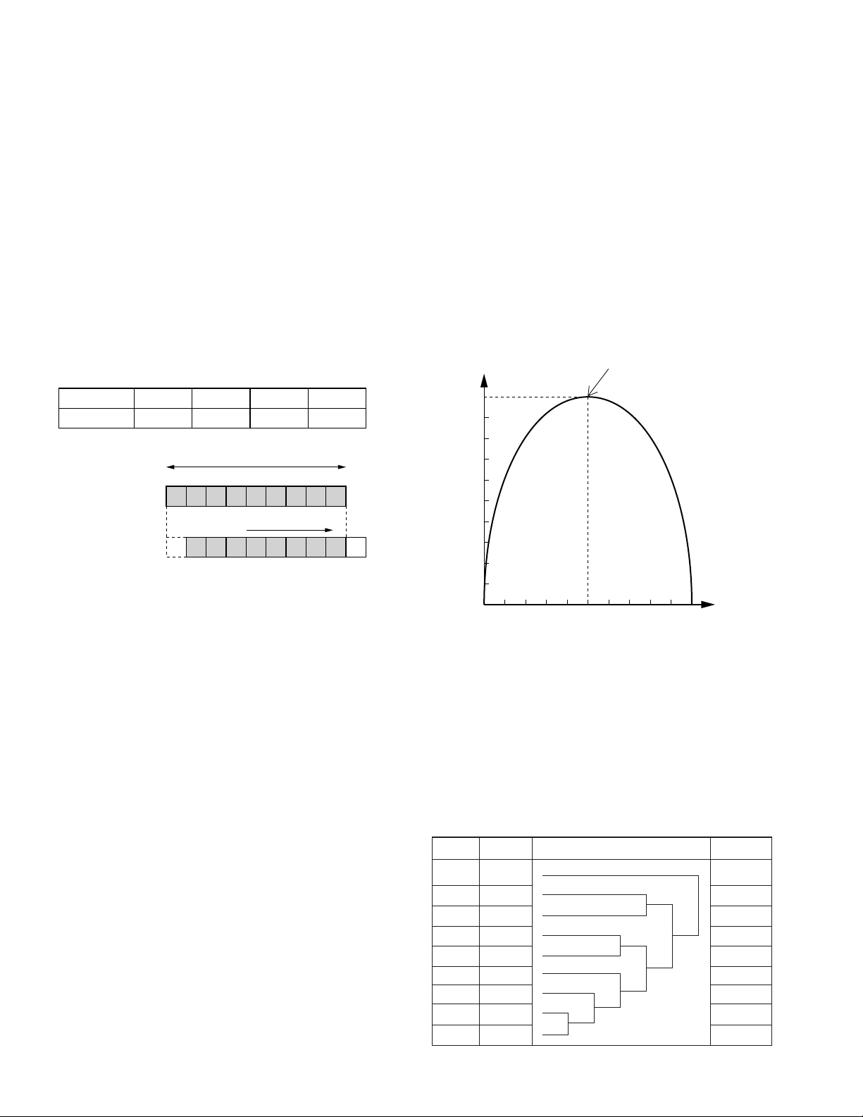
Table 8-1-1 outlines comparisons between DV and other digital VCR formats.
D9 (Digital S) DVC Pro DV CAM DV
Material MP ME
Tape
Sampling frequency
(MHz)
Sampling rate
Width (inch) 1/2 1/4
Track pitch (µm) 20
Y 13.5
R-Y/B-Y 6.75 3.375
NTSC
PAL
4 : 2 : 2
18 15 10
4 : 1 : 1
4 : 2 : 0 (Line Sequential)
Video
Audio
Error correction code
Modulation method
As shown in the above table, the major specifications of the DV
are almost identical to the D9 (Digital S).
Differences lie only in the tape used, sampling rate and number
of executed pixels.
Samples per line
TV lines per frame
Quantization bits
Compression method
Compression
Sampling frequency (kHz)
Quantization bits
Channels
Compression
Y 720
R-Y/B-Y 360 180 : NTSC,360 : PAL
NTSC
PAL
Table 8-1-1 Comparison of Digital VCR Formats
482
578
1/3.3
48
16
4
480
576 : Y , 288 : R-Y/B-Y
8
In-frame DCT
1/5
48(32)
16(12)
2(4)
Non compressed
Reed-Solomon integration code
SI-NRZI , 24/25
(A) Video signal
High video quality thanks to the 4:1:1 (*4:2:0) component digital recording.
(Note) Descriptions marked * in the text and figures are PAL
data.
• Luminance signal
The Y signal is sampled at 13.5 MHz so the Y signal bandwidth
is about half the sampling frequency, or 6.75 MHz. This provides better resolution than S-VHS and current TV broadcasting
(Y bandwidth of about 4.5 MHz).
8-1
Page 2
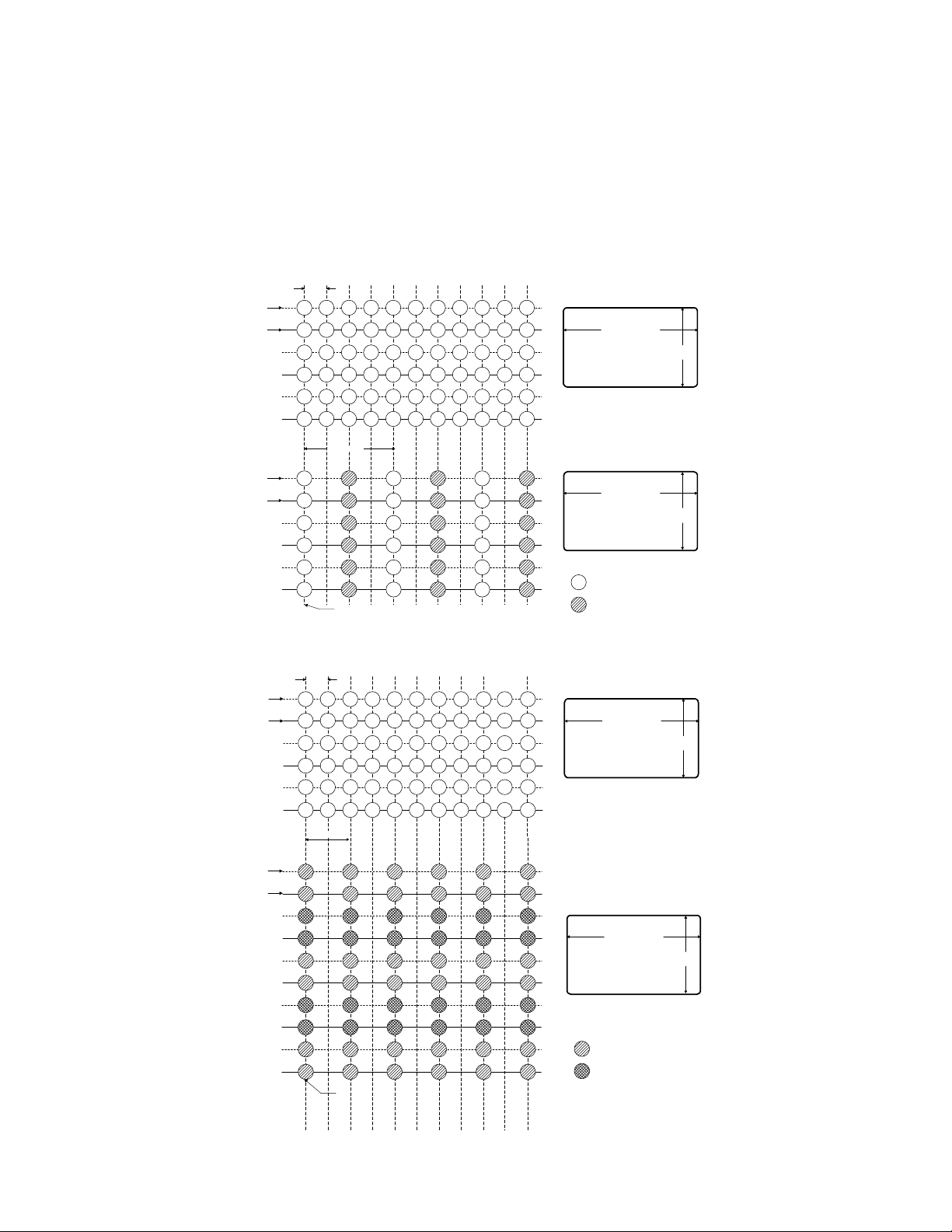
• Chrominance signal
By recording the chrominance signal in a form divided into color
difference signals R-Y and B-Y (component recording method),
recording with excellent color reproduction and little color blur
is achieved.
MHz
Y Signal
First effective line
in each field
Colour difference
Signal (CR, CB)
First effective line
in each field
1/13.5
MHz
1/3.375
First pixel in the effective period
With VHS, the chrominance signal has been converted into a
lower-frequency signal so that its bandwidth has been limited
to 0.5 MHz. The DV has expanded the bandwidth by about 3
times to 1.68 MHz (3.375MHz/2) and records the chrominance
components quite separately from the Y component. The sampling frequency of the R-Y and B-Y signals are 3.375 MHz (*6.75
MHz), which is 1/4 (*1/2) of the Y signal sampling frequency of
13.5 MHz. Based on this ratio, this recording method is referred
to as 4:1:1 (*4:2:0 line sequential) digital component recording.
Line
285
Line
23
Line
286
Line
24
Line
287
Line
25
Line
285
Line
23
Line
286
Line
24
Line
287
Line
25
720 Samples
180 Samples
4:1:1 Sampling
: Effective sample
: Interlaced sample
480 Samples
480 Samples
X2
Y Signal
First effective line
in each field
Colour difference
Signal (CR, CB)
First effective line
in each field
Fig. 8-1-1 4:1:1 Component Digital Recording
MHz
1/13.5
Line
335
Line
23
Line
336
Line
24
Line
337
Line
25
MHz
1/6.75
Line
335
Line
23
Line
336
Line
24
Line
337
Line
25
Line
338
Line
26
Line
339
Line
27
First pixel in the effective period
720 Samples
360 Samples
4:2:0 Sampling
: CR
: CB
576 Samples
288 Samples
X2
8-2
Fig. 8-1-2 *4:2:0 Component Digital Recording
Page 3
(B) Audio signal
The DV format also records the audio digitally. Two recording
formats (48 kHz, 32 kHz) are provided to allow selection according to the purpose. Compatibility with 44.1 kHz sampling is also
provided for use in the reproduction of software tapes.
• 48 kHz, 16-bit high quality stereo mode
This recording mode provides high audio quality equivalent to
the DAT.
Although compression technology is used in video recording,
the audio recording does not use compression.
• 32 kHz, 12-bit mode with a stereo dubbing capability
This mode divides the audio area into two parts and records 12bit stereo audio channels to both of them, or a total of 4 channels. This makes it possible to record 2 audio channels at the
same time as performing video recording and to dub 2 additional audio channels while leaving the original audio channels.
(C) Other features
• Video signal output
The digital signal read out from a tape during playback is fed to
the image memory to arrange the time axis before being output
as the video signal. This makes it possible to reduce wow &
flutter, which may be caused by head rotation irregularities or
tape transport variations.
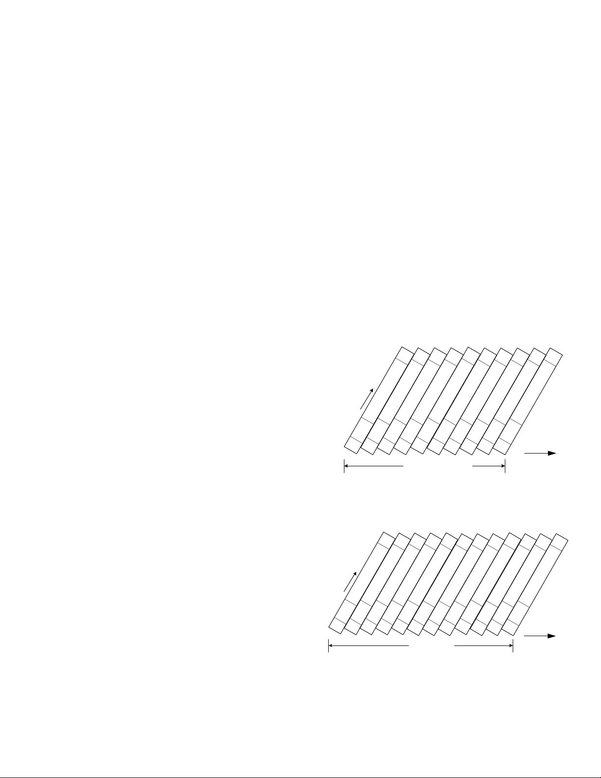
8.1.2 Tape Format of DV
Note) Descriptions marked * in the text and figures are PAL
data.
The DV records the video and audio signals independently, in
the video area and in the audio area respectively. With the video
signal, the data of each frame is divided into 10 tracks (*12 tracks)
before being recorded. Namely, the data of a frame is input to a
memory, divided into 10 (*12), and recorded into 10 tracks (*12
tracks) using a 2-channel head by rotating the drum by 5 turns
(*6 turns) in the period of one frame (33.3 ms/*40 ms) of a
normal NTSC (*PAL) signal. The sub-code area records data including the timecode, recording date, index and absolute track
number, and the ITI area records the reference signal of the
absolute height of track (SSA) ad tracking signals. The DV does
not use the tracking control track. The tracking system of the
DV is called the 3-frequency (F0, F1, F2) digital pilot system,
which records digital pilot signals F0 (0Hz), F1 (465 kHz) or
F2 (697.5 kHz) on every track during recording. When the F0
track is reproduced, the DV controls the tracking servo so that
the crosstalk levels of the pilot signals (F1, F2) in the tracks on
the left and right of the F0 track become identical. The pilot
signals are recorded over all the tracks.
Sub
• Timecode enabling editing
The DV tape has a sub-code area for recording signals for use in
editing. Timecodes are automatically recorded frame by frame
in this area so that the video can later be edited on a per-frame
basis. The sub-code area also includes the recording of index ID
signals, which can be used in search and other operations later.
• AUX data recording information on recording and shooting
The video signal recording area on the tape records the signal
called the AUX data together with the video signal. The AUX
data contains information on the recording date and shooting
conditions such as wide-screen shooting, and is recorded automatically during recording. Parts of the AUX data information
can be displayed on the screen as required. The AUX data on
the record mode, etc. is also recorded in the audio area in a
similar way to the video area.
• Digital interface for digital inputs/outputs (optional)
All track data can be input or output directly without altering the
digital format (IEEE1394 compliant).
DV terminals are provided to enable dubbing and editing using
digital signals.
Video
Head writing
Audio
ITI
F0 F0 F0 F0 F0F1 F2 F1 F1F2
10 tracks/frame
Fig. 8-1-3 NTSC Format DV Tape
Sub
Video
Head writing
Audio
ITI
F0 F0 F0 F0 F0F1 F2 F1 F1F2 F0 F2
12 tracks/frame
Tape travel
Tape travel
Fig. 8-1-4 PAL Format DV Tape
8-3
Page 4
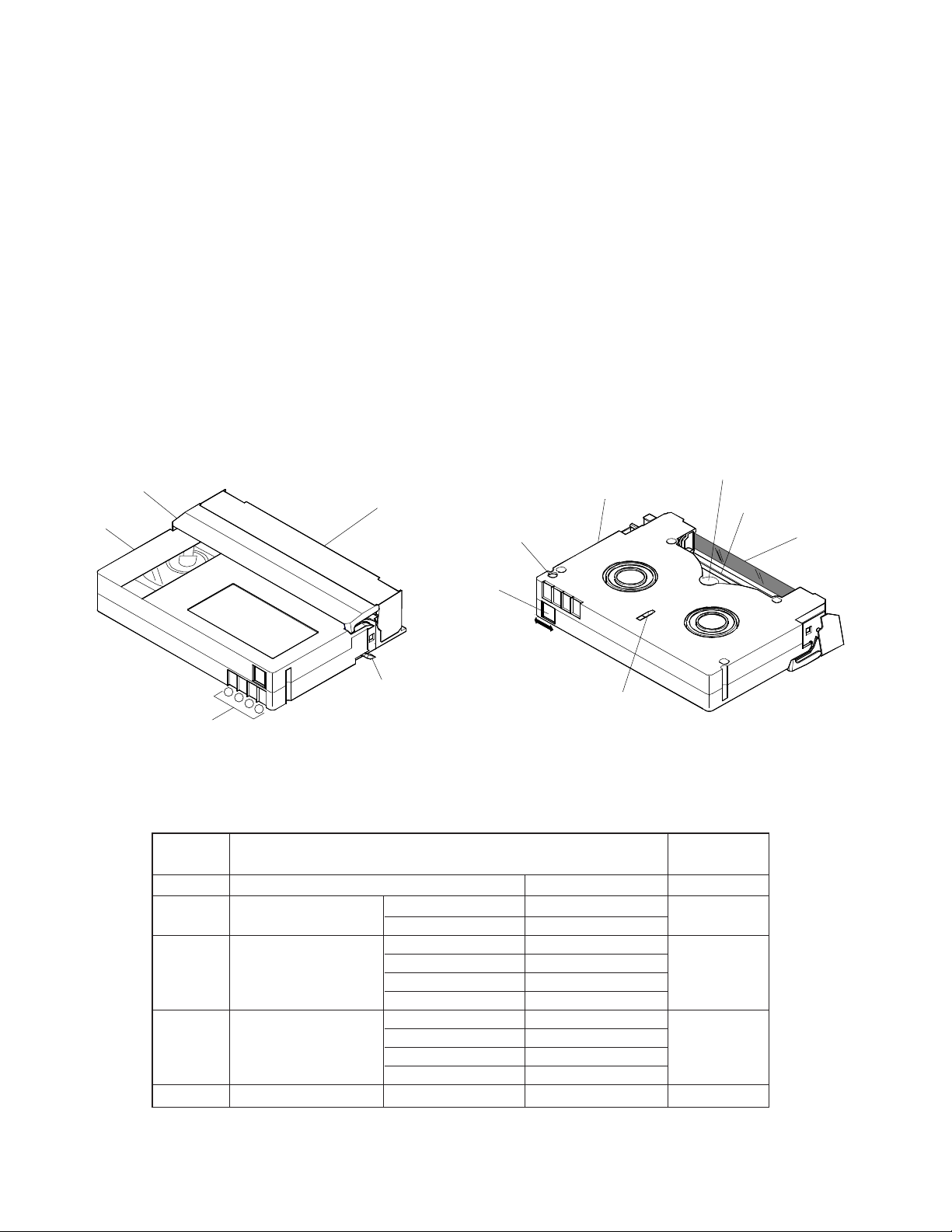
(A) Mini-DV cassette tape
The DV cassette uses metallic magnetic particles so that stable, high-power signals can be obtained from even very thin
tracks. Metal tapes include the metal particle coated (MP) tapes
and metal evaporated (ME) tapes. The Metal tape used with the
DV is the ME tape which features a thin magnetic layer and low
demagnetization.
• ID board and memory-in cassette (MIC)
The DV cassette has 4-contact terminals on the back label side
edge of the shell. These terminals are called the “ID board terminals”, and the values of resistance across the terminals express basic cassette ID (BCID) information such as the tape thickness, tape type and applications. The DV cassette can optionally incorporate a memory for storing the BCID as well as the
content information. In this case, these 4 terminals are used as
the serial communication terminals for the storage and readout
of cassette memory contents.
As described above, the ID board terminals are used in two
ways and the cassettes are available as those with or without
internal memory according to the usage. The GY-DV500 and
BR-DV600 are not avairable with this optional function, so information such as the content information cannot be written or
read even when a cassette with internal memory is used with
them.
All these models do through these terminals is read the BCID of
every cassette.
Upper shell
Top lid
ID board terminal
Terminal
No
1
2
3
4
1
2
3
4
thickness
Tape type
Tape grade
Front lid
Accidental erasure
protection hole
Accidental erasure
protection tab
Open
REC possible : Close
REC impossible: Open
Lid lock
Fig. 8-1-5 External View of Mini-DV Cassette
Contents
Tape
7µm
Reserved
ME
Reserved
For cleaning
MP
For consumer
For professional
Reserved
For PC
–
LED hole
Lower shell
Close
Reel lock
MICID Board
Resistor value Function
Open
1.80kΩ ± 0.09k
VDD
Open
6.80kΩ ± 0.34k
1.80kΩ ± 0.09k
SDA
S/C
Open
6.80kΩ ± 0.34k
1.80kΩ ± 0.09k
SCK
S/C
–
GNDGND
Bottom lid
Tape
8-4
Table 8-1-2 ID Board Terminal Standard
Page 5
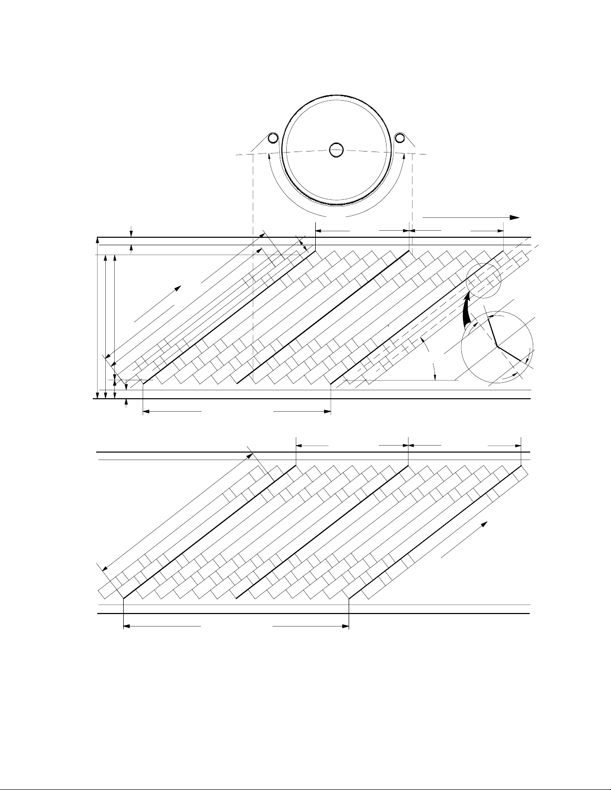
(B) Main Standard of DV Tape Format (SD)
θr
Tape travel (Ts)
A ch 1
(ch 1, 2)
Sub
Code
G3
A ch 1
(ch 1, 2)
MRG
α1
α2
174°
A ch 2
(ch 3, 4)
Video
0
F0
Opt. track 2
Video
G1
ITI
9
F2
(PF1)
A ch 2
(ch 3, 4)
G3
Audio
8
F0
Sub
G2
Code
MRG
MRG
Sub
Code
G3
Video
H2
Head motion
Lr (θe)
Wt
H0
(We)
1
0
F2
F0
He
H1
(PF1)
Effective data area (NTSC: 134975 bit)
G2
Audio
G1
ITI
8
9
F0
F1
6
7
F0
F2
1 Frm (Pilot Frm 0)
525/60
ITI
5
F1
Opt. track 1
G1
Video
4
F0
Audio
ITI
Tp
MRG
Sub
Code
G3
G2
G2
Audio
G1
2
3
F2
1
F0
F1
Opt. track 2
MRG
Sub
Code
G3
MRG
Sub
Code
G3
MRG
Sub
Code
G3
MRG
Sub
Code
G3
1
F1
(PF0)
Effective data area (PAL: 134850 bit)
Audio
G1
ITI
0
11
F0
10
F2
F0
Video
G2
9
8
F1
F0
ITI
6
7
F0
F2
G2
G2
Audio
Audio
G1
G1
ITI
3
4
5
F0
F1
2
F2
F0
Video
1
F1
Video
0
F0
G2
Audio
G1
ITI
11
F2
Video
Opt. track 1
1 Frm (Pilot Frm 0)
625/50
(PF0)
Fig. 8-1-6 Main Standard of DV Tape Format (SD) (Track Pattern)
Head motion
8-5
Page 6
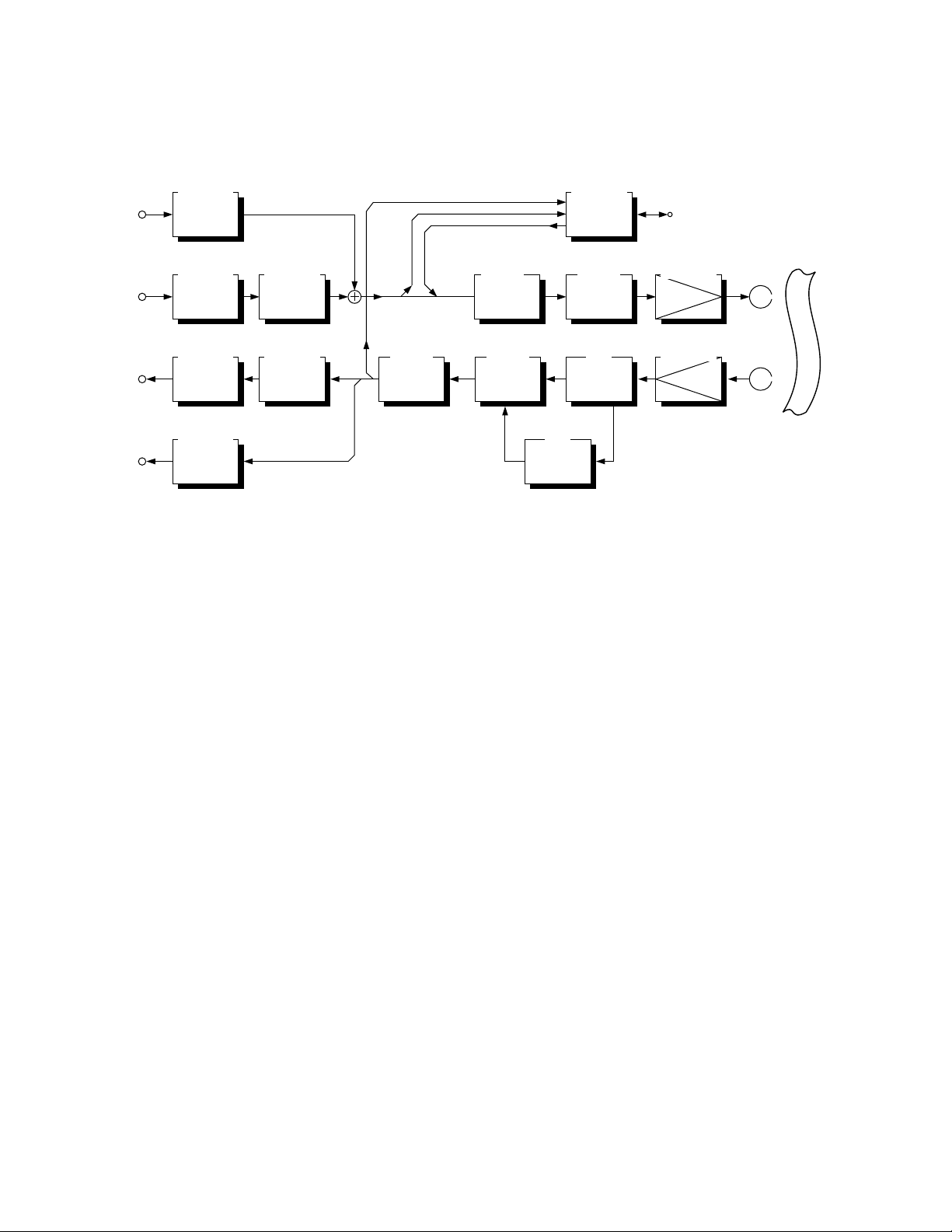
8.2
MAJOR SIGNAL PROCESSING OPERATIONS OF DV
Fig. 8-2-1 shows the basic configuration of the major signal
processing circuitry of the DV in the form of a block diagram.
SHUFFLE
SHUFFLINGAUDIO
VIDEO
VIDEO
AUDIO
SHUFFLE
MACRO BLOCK
SHUFFLING
DESHUF.
DESHUFFLING
DESHUF.
DESHUFFLING
CODING
DCT
VLC
DECODING
I-DCT
VLD
ECC
INNER
OUTER
SHUFFLING
Fig. 8-2-1 Basic Configuration of Major Signal Processing Circuitry of DV
8.2.1 Flow of Video and Audio Signals in Recording Circuitry
The video and audio signal inputs/outputs shown in Fig. 8-2-1
are sampled digital signals.
The input digital video signal is shuffled block by block, so that
deviations in the compression rate of the picture can be prevented. This is achieved by gathering data from various positions in the picture and compressing it. When the video signal is
supplied to the ECC block for error correction later, de-shuffling
is applied to return the data to the original positions in the video
signal. The shuffled video signal is coded. The coding consists
of replacing the image signal in the conversion block composed
of multiple pixels with signals without correlation by means of
discrete cosine transform (DCT).
The DCT operation consists of dividing the picture into blocks
(each composed of 8 x 8 pixels) and obtaining the transform
coefficient, which indicates the amount of components of the
previously determined basic image pattern (64 pixels) in each
block.
The VLC (Variable Length Coding) quantizes the DCT transformed
signal and applies entropy coding to the quantized signal. The
coding technique used here performs Run Length coding first,
then applies Huffman coding.
The audio input signal is also shuffled block by block in the same
way as with the video signal, but the audio signal is not compressed.
The video and audio signals are input to the ECC block, where
error-correcting codes are appended to them. The error-correcting codes use product codes obtained by double coding of the
Reed-Solomon integration codes.
The DCI-R (Digital Channel Interface for Recording) block performs channel coding of the recorded signals. It performs what
IEEE1394
I/F DV TERMINAL
TG
SERVO
DCI-R
SI-NRZI
24/25
Phase &
Amplitude
Compensator
ECC
OUTER
INNER
DESHUFFLING
DCI-P EQ
3 TO 2
1+D
VITERBI
TRACKING
Note : PAL model is not available the signal output.
See note:
REC.AMP. HEAD
PRE-AMP.
HEAD
TAPE
is usually called modulation by transforming a series of digital
data composed of “1” and “0” to match the properties of magnetic recording systems.
8.2.2 Flow of Video and Audio Signals in Playback Circuitry
When a digital VCR plays a recorded signal, the frequency response of the low-frequency and high-frequency components
is degraded. The degradation in the frequency response of the
low-frequency components is because the played signal becomes a differential waveform and a rotary transformer is used.
That in the frequency response of the high-frequency components is caused by the performance of the recording tape itself
and by the gap between the tape and head during recording/
playback.
When a tape in which 1-bit pulses are recorded is played while
the frequency response is degraded, the pulse duration is expanded and intersymbol interference results. The equalizer is
used to suppress the intersymbol interference and reduce code
errors.
The DCI-P (Digital Channel Interface for Playback) block demodulates the signal, which has been coded for recording and turns it
into a signal that can be subjected to error correction.
The ECC (Error Correcting Codes) block corrects errors while
performing shuffling. The audio signal is then de-shuffled and
output. The video signal is sent to the decoding block where
the signal compressed by coding is expanded by means of decoding, and returns to a digital signal. The digital video signal is
then de-shuffled before being output.
8-6
Page 7
8.3 VIDEO/AUDIO SIGNAL PROCESSING IN
RECORDING CIRCUITRY
8.3.1 Division into Blocks
As shown in Fig. 8-3-1, data of each frame is divided into
macroblocks (MBs) (8 x 8 pixels) which are the basis of the DCT
circuitry. Since the luminance signal and two color difference
signals are sampled with different frequencies, 4-luminance signal blocks and each of the color difference signal blocks occupy
the same position and area in the picture. When data of any one
of the 4-luminance signal blocks is lost, the data in other blocks
becomes meaningless. Therefore, the signals of every 6 blocks
are processed as a single processing unit and recorded onto
tape.
(a) With a 525/60 system:
90 (22.5) blocks
(b) With a 625/50 system:
90 (45) blocks
8.3.2 Shuffling (Video)
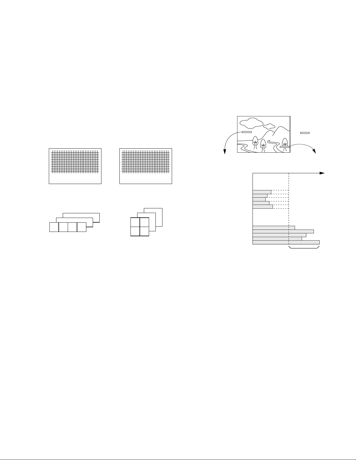
The 5 macroblocks composing a single video segment is collected from a picture by means of shuffling according to a specified rule.
The objective of shuffling lies in making uniform the quantity of
information that is contained in the 5 macroblocks in a video
segment. The image information of a frame is not usually distributed evenly in the picture, but there are segments with a
large amount of information and those with a small amount of
information as shown in Fig. 8-3-2.
5MB
60 (60)
blocks
Figures inside ( ) are the number of color difference (CR, CB) blocks.
Macroblock
CB
CR
Y
8
8
8 8 8
8
8
Six blocks occupying the same position and
area in the picture form a macroblock.
8
72 (36)
blocks
8
Macroblock
CB
8
R
8
C
Y
8
8
8 8
8
8
Fig. 8-3-1 Division into Blocks, Macroblock
The macroblock is a group composed of the 6 blocks.
The data divided into blocks is processed by the DCT coding as
described later, and the video-recording rate is compressed to
25 Mbps. In fact, however, the data of each frame is compressed
to the specified number of bits, which are recorded onto the
specified number of tracks on tape. Namely, when 25 Mbps is
converted into the number of bits per frame, the following
number of bits are recorded onto 10 (NTSC) or 12 (PAL) tracks:
(25 x 10
(25 x 10
6
)/30 = 833333 bits ............ (NTSC)
6
)/25 = 1000000 bits .......... (PAL)
As seen above, the data in each frame is compressed so as not
to exceed the specified number of bits calculated based on the
video-recording rate. This is referred to as length fixation. Although the length of the data of a frame is fixed so as not to
exceed the calculated number of bits, the actual length fixation
is applied per 5 macroblocks. In other words, the length of the
data of 5 macroblocks is fixed so as not to exceed the following
number of bits:
833333 x 5/1350 = 3086 bits ......... (NTSC)
1000000 x 5/1620 = 3086 bits ....... (PAL)
The 5 macroblocks used as the unit of length fixation is referred
to as a video segment.
Video segment A
(Flat, sky section)
Video segment A
(Few information)
Video segment B
(Much information)
MB1
MB2
MB3
MB4
MB5
MB1
MB2
MB3
MB4
MB5
Length fixation information
Video segment B
(Fine branch section)
Coarse quantization for
reducing the amount of
information
Fig. 8-3-2 Distribution of Information in a Picture
As a result, if the fixed-length data obtained from 5 sequential
macroblocks uses the same number of bits for each macroblock,
distortion due to compression or expansion of data would be
noticeable. This would depend on the screen segments (distortion is less noticeable in the segments with little information
but noticeable in segments with much information). To prevent
this by making the information uniform across the video segments and making distortion less noticeable, shuffling is performed in the picture.
The shuffling is performed based on the rule shown in Fig. 8-3-
3.
Each picture is divided vertically into the same number as the
number of macroblocks in a video segment (5), and divided horizontally into the same number as the number of tracks used to
record the data of 1 frame onto tape (NTSC: 10, PAL: 12).
The blocks divided in this way are referred to as superblocks.
8-7
Page 8
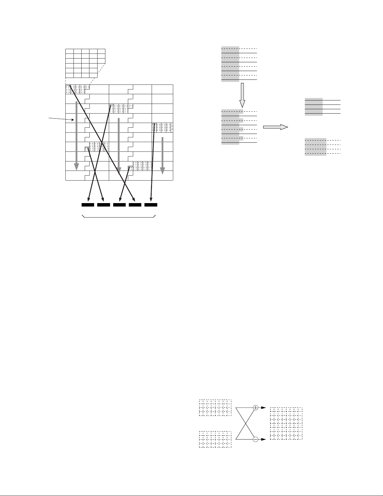
Sequence of MBs in a superblock
No.
0
11
12
23
1
10
2
9
3
8
4
7
5
6
24
13
22
25
14
21
26
15
20
16
19
17
18
8 pixels
2nd Field
1st Field
8 lines
Sequence of
superblocks
Order of shuffling
12 34 5
MB1 MB2 MB3 MB4 MB5
Set at a fixed length of 5 MBs.
Fig. 8-3-3 Shuffling Technique (Example with 525/60)
With shuffling, the first macroblock (No. 0) in each of the 5
superblocks are collected to form a video segment as shown in
Fig. 8-3-3, and the next video segment is formed by collecting
the first macroblocks (No. 1) of the same 5 superblocks. When
all of the macroblocks in the 5 superblocks have been collected,
data collection of the next 5 superblocks starts.
8.3.3 DCT
The video segments formed by shuffling are DCT transformed
per (8 x 8) blocks. There are two DCT transform modes including the stationary mode and the dynamic mode.
(1) Stationary mode (8 x 8 DCT mode)
This is the basic mode, executing (8 x 8) DCT transform to
every (8 x 8) pixels in blocks.
(2) Dynamic mode (2 x 4 x 8 DCT mode)
The (8 x 8) blocks are divided into two (4 x 4) blocks called
fields 1 and 2, and a (4 x 8) DCT transform is applied to every
(4 x 8) pixels.
The following paragraph explains this mode by taking the
case in which an object moves toward the right as an example.
When the object
moves horizontally:
The vertical high-frequency
component increases.
4 lines
(2 x 4 x 8)
4 lines
8 pixels
(1st Field)
8 pixels
(2nd Field)
Fig. 8-3-4 (2 x 4 x 8) DCT Transform in Motion Mode
When the object does not move, the data in the horizontal direction contains the high-frequency component but the data in
the vertical direction contains only the DC current. On the other
hand, when the object moves in the horizontal direction, the
position of the object at the time of 1st field scanning is different from that at the time of 2nd field scanning, so the picture of
the object in a frame appears to have ridged edges. The highfrequency component increases in the vertical direction data as
well as in the horizontal direction data. In such a case, the (8 x 8)
blocks are divided into two pairs of (4 x 8) blocks for fields 1 and
2, and (4 x 8) DCT transform is applied to every (4 x 8) pixels.
This method makes it possible to reduce any increases in the
high-frequency component in the vertical direction data and prevents a drop in the compression rate.
Whether a DCT transform is performed in the stationary mode
or in the dynamic mode is decided by detecting the (8 x 8) blocks
in each video segment by the motion detector circuit located
before the DCT transform circuit.
The data of a block in stationary mode is composed of one DC
component and 63 AC components. But, in dynamic mode each
one of the two (4 x 8) blocks is composed of a DC component
and 31 AC components. To allow the dynamic mode data to be
processed in the same way as the stationary mode data, the
dynamic mode processing calculates the sum and differences
of the factors of the same order and form (8x 8) blocks as shown
in Fig. 8-3-5.
(2 x 4 x 8) DCT factors
8
4
(1st field)
8
4
8
(Sum of factors)
8
(Difference of factors)
8-8
(2nd field)
Fig. 8-3-5 Processing of DCT Transform Factors in Dynamic Mode
Page 9
The above processing allows both the dynamic mode data and
0
0
1
2
4
7
6
5
3
0
0
1
1
2
2
2
1
0
1
1
2
3
2
2
1
1
1
1
2
3
3
2
2
1
1
2
2
3
3
3
2
1
2
2
3
3
3
3
2
2
2
2
3
3
3
3
3
2
2
3
3
3
3
3
3
DC
0
0
1
2
2
1
1
1234567
(8 x 8) DCT
Vertical direction
0
0
1
2
3
0
1
1
2
1
1
2
2
1
2
2
2
1
2
2
3
2
2
3
3
2
3
3
3
3
3
3
3
DC
0
1
1
1234567
(2 x 4 x 8) DCT
Horizontal direction
(Sum)
4
7
6
5
0
2
1
1
1
2
2
1
1
3
2
2
2
3
2
2
2
3
3
2
2
3
3
3
3
3
3
3
0
1
1
0
Vertical direction
(Difference)
Class No. Area No.
0
15
14
13
12
11
10
9
8
7
6
5
4
3
2
1
0
1
15
14
13
12
11
10
9
8
7
6
5
4
3
2
1
0
2
15
14
13
12
11
10
9
8
7
6
5
4
3
2
1
0
3
15
14
13
12
11
10
9
8
7
6
5
4
3
2
1
0
0
1
1
1
1
1
1
1
1
1
1
1
1
2
2
2
2
4
4
4
4
8
8
1
1
1
1
1
1
1
1
1
1
1
2
2
2
2
4
4
4
4
8
8
8
8
2
1
1
1
1
1
1
1
1
2
2
2
2
4
4
4
4
8
8
8
8
16
16
3
1
1
1
1
1
1
1
2
2
2
4
4
4
4
8
8
8
8
16
16
16
16
Quantizer No.
Horizontal direction
stationary mode data to be handled as data composed of one
DC component and 63 AC components in the subsequent
quantization processing.
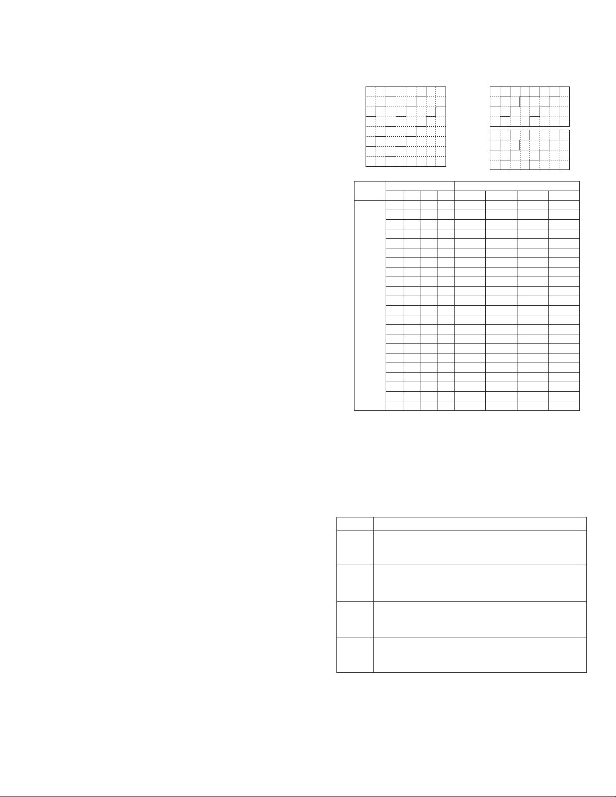
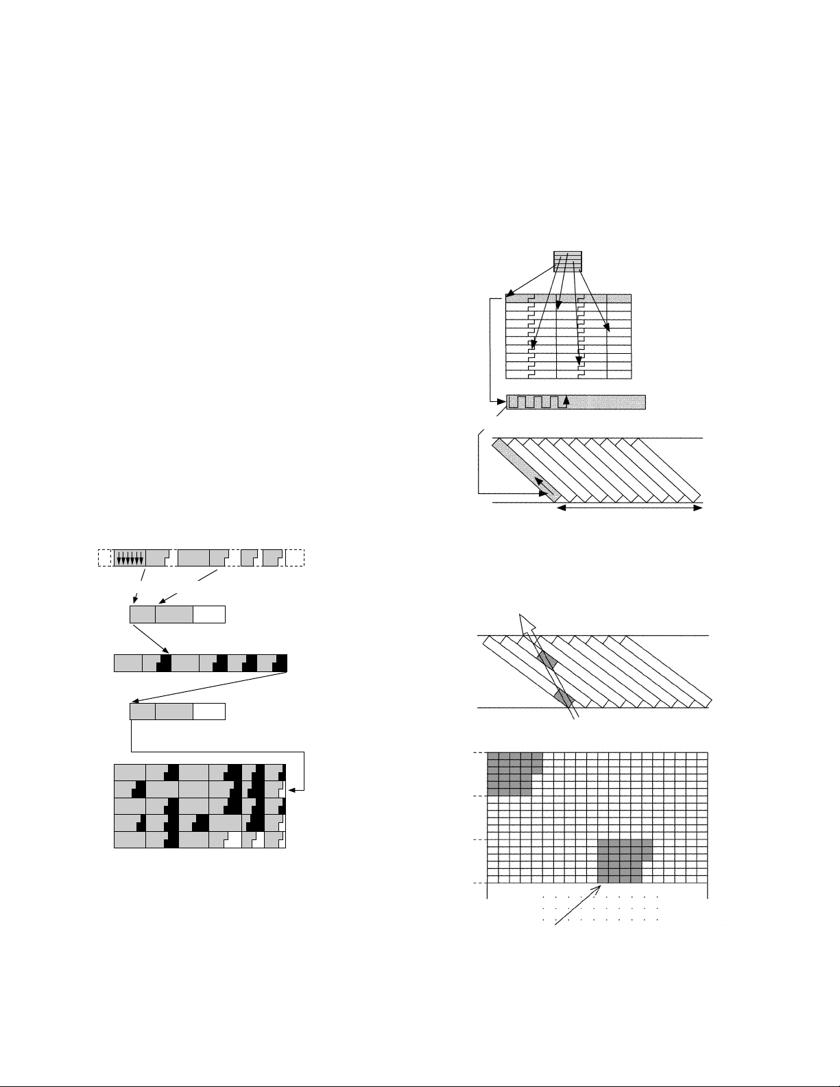
8.3.4 Quantization
(A) Data quantity estimation
After all of the blocks in a video segment have been DCT transformed, the video segment is stored in the buffer. At this time,
the data quantity estimation block selects the quantizer for use
in quantizing the video segment.
With DCT transform, normalization is performed so that the DCT
factors have a 10-bit dynamic range for the 8-bit pixel block. The
DCT factors are divided by an integer called the quantization
step and allocated to a smaller number of bits before being subjected to variable-length coding (VLC). This operation (division)
is referred to as re-quantization, or simply quantization. The
quantization reduces the values of the factors, turning many of
0 in the high frequencies. As the VLC in the subsequent stage
performs code allocation by forming value 0 run lengths and the
non-0 factor after it into a group, so the quantization improves
the coding efficiency. As the VLC consists of simply allocating
codes to factors, the code quantity (number of bits) is controlled by the VLC block.
(B) Quantization
Each quantizer is composed of a set of 4 quantization steps as
shown in Fig. 8-3-6, and the factors in a block are divided into 4
areas. The data is quantized in the 4 areas using different
quantization steps. The factors are shifted from low-frequency
factors to high-frequency factors as the area number increases,
so the quantization of high-frequency factors are coarser than
for low-frequency factors. This utilizes the fact that the distortion of high-frequency factors is less noticeable to human vision
even when they are coarsely quantized.
Fig. 8-3-6
(C) Classification
Each block in a video segment is classified into one of 4 classes
before being quantized. The quantization steps of the quantizers
vary depending on the class numbers (see Fig. 8-3-6). Table 8-31 shows the definitions of the 4 classes.
Class No.
0
1
2
3
Block with which quantization distortion after compression is highly noticeable. The absolute value of the AC
factor should not exceed 225.
Block with which quantization distortion after compression is less noticeable than Class 0. The absolute value of
the AC factor should not exceed 225.
Block with which quantization distortion after compression is less noticeable than Class 1. The absolute value of
the AC factor should not exceed 225.
Block with which quantization distortion after compression is little noticeable or the absolute value of the AC
factor exceeds 225.
Definition
Table 8-3-1 Definitions for Classification
8-9
Page 10
The Table 8-3-1 means that a block with a larger class number
has a more approximate degree of definition (activity). The data
in such a block is quantized relatively roughly to compress the
data quantity. Rather approximate quantization of picture areas
with low activity does not cause odd sensations for the human
vision, but approximate quantization of those with high activity
does cause odd sensations. The blocks with low activity in each
segment are quantized as roughly as possible with a reduced
number of allocated bits, unless the odd sensations are not felt.
However, the blocks with high activity are quantized using an
increased number of allocated bits to improve the picture quality experienced by the human vision.
A block containing factors with a larger absolute AC factor than
255 is classified as Class 3, and subjected to an operation called
initial shifting before quantization. This operation divides an AC
factor over 255 by 2 so that errors do not occur in the VLC operation.
Class No.
Initial shifting
Before initial shifting
MSB=1
(ACmax > 255)
After initial shifting
0
Not applied1Not applied2Not applied
9 bits
MSB LSB
1
1-bit shift
01
The value is accommodated within 8 bits.
3
Applied
Fig. 8-3-7 Initial Shifting
While the AC factor before quantization consists of 10 bits, or 9
bits excluding the sign bit, the VLC in the subsequent stage can
codify a non-0 factor value only into an 8-bit code. Initial shifting
is performed to deal with this. As a result, a factor that has a
value in the 9th bit (SMB) (i.e. a factor over 255) can be accommodated in 8 bits and processed by VLC. Fig. 8-3-6 shows that
an increase in the class No. increases the quantization steps in
the same quantizer No. or that quantization of a larger class No.
is more approximate.
Although the quantization steps of Class 2 look less than for
those of Class 3, this is because the Class 3 data has been
subjected to initial shifting before quantization. The actual
quantization steps of Class 3 are more approximate than in those
of Class 2.
8.3.5 VLC
After division into (8 x 8) blocks by DCT transform, the energy
of pixels are concentrated in the DC component and the vertical
and horizontal vertical factors become almost null. To code these
factors, coding uses a technique for varying the code length
according to the incidence of the factors.
This coding technique varying the code length is referred to as
variable length coding (VLC).
(A) Entropy coding
As the VLC achieves efficient coding by allocating short codes
to data with a high DCT factor incidence and long codes to data
with a low incidence, it is sometimes called the entropy coding.
The entropy coding can be expressed with an entropy function.
H = 1 (max.) when Pn = 0.5 (when 0 and 1
both occur at the same probability)
H
1.0
0.9
0.8
0.7
0.6
0.5
0.4
0.3
0.2
0.1
0 0.1
0.2 0.3 0.4 0.5 0.6 0.7 0.8 0.9 1.0
0
P
Fig. 8-3-8 Entropy Function
When VLC approaches the above function, it is regarded as coding with a high compression rate.
(B) Huffman coding
The DV uses Huffman codes to improve the compression efficiency. The Huffman codes determines the minimum average
code length of information with a known incidence probability.
Table 8-3-2 shows the method of construction of Huffman codes.
The symbols in the table should be regarded as the levels of
pixel values.
Symbol Incidence Code Word
1
0.49
2
0.14
3
0.14
4
0.07
5
0.07
6
0.04
7
0.02
8
0.02
9
0.01
Construction Procedure
0
0
1
0
0
1
0
0
0
1
0
1
1
1
1
0
100
101
1
1100
1101
1110
11110
111110
111111
8-10
Table 8-3-2 Construction of Huffman Codes
Page 11
The Huffman coding uses the following procedure.
Mode Channels Sampling Frequency
48 k
44.1 k
32 k
32 k
2
4
48 kHz
44.1 kHz
32 kHz
32 kHz
16-bit linear
12-bit nonlinear
Quantization
(1) Information source symbols 1 to 9 are arranged in the order
of incidence probability.
(2) For the symbol with the lowest incidence and that with the
second-lowest incidence, “0” is allocated to one and “1” is
allocated to the other. (Which of the two symbols is “0” and
which is “1” can be decided arbitrarily.)
(3) Then, the above two symbols are considered to be joined
together as a single symbol. The incidence probability of the
joined symbols should be equal to the sum of the incidence
probabilities of the two symbols before joining.
(4) By considering the joined symbols as new individual sym-
bols, these symbols and other symbols (which should exclude the two symbols which were joined) are rearranged in
the order of incidence probability.
(5) Steps (2) to (4) are repeated until the number of symbols
becomes 1.
(6) The values (0 or 1) allocated to the original symbols in step
(2) are read in the reverse order. The read values form the
code word for the symbols.
255
15
10
5
Factor Value <Absolute Value>
0
1 2 3 4 5 6 61 62 6378
Order of Zigzag Scanning
Factor series = {0, 12, 5, 0, 0, 0, 4, 3,... 0, 0, 0}
Transform into (0 run length + non-0 factor values)
(1, 12), (0, 5), (3, 4), (0, 3)... (EOB)
A Huffman code constructed in this way can be decoded instantaneously because, by following the bits one by one from
the first bit at the time of decoding, the end of a code word can
be determined without referring to the head of the next code
word.
As the VLC used with the DV is based on Huffman coding combined with run length coding, it is called “modified 2-dimensional Huffman coding”.
Horizontal frequency
Vertical frequency
Fig. 8-3-9 Zigzag Scanning of DCT Factors
Among the factors transformed by 2D DCT, the 63 AC factors
other than the DC component factor are rearranged by zigzag
scanning as shown in Fig. 8-3-9. When the AC factors are rearranged in the order of scanning, the result is as shown in Fig.
8-3-10, where the scanned factor series is divided into a group
of sequential 0 factors followed by a group of non-0 factors. A
code called the EOB (End Of Block) is appended after the last
non-0 factor scanned.
After the factors are transformed into a group of 0-value run
length and a group of non-0 factor values, a Huffman code table
is compiled according to the incidence probabilities of these
groups and VLC is applied based on this.
VLC
(111011s), (100s), (11011s),... (1110)
s: Sign bit
Fig. 8-3-10 2D Huffman Coding
8.3.6 Shuffling (Audio)
Unlike the video signal, the audio signal is not compressed. It is
subjected only to shuffling as preparation for the ECC.
Table 8-3-3 shows the basic modes of the DV.
Table 8-3-3 Basic Audio Modes
In the 2-channel modes, the quantization is 16-bit linear and the
sampling frequency can be selected from 48 kHz, 44.1 kHz or
32 kHz. One of the 2 channels is recorded in the first 5 tracks of
the 10 tracks of an NTSC frame (first 6 tracks of the 12 tracks of
a PAL frame) after shuffling. Therefore, when an error occurs
with a track, 1/5 (or 1/6) interpolation is applied.
8-11
Page 12
8.3.7 De-shuffling
The compressed video data is recorded on tracks on tape. The
video data recording area of each track is divided into sub-units
called the sync blocks (SBs). The number of SBs where video
data is recorded is 135 per track, and the number of SBs per
frame is:
135 x 10 = 1350 ............................. (NTSC)
130 x 12 = 1620 ............................. (PAL)
These values are equal to the number of macroblocks per frame.
Therefore, the compressed video segment data (5 macroblocks)
is packed into 5 SBs and recorded.
Fig. 8-3-11 shows the packing of video segment data into 5 SBs.
<Step 1>
• The macroblock data is packed into the specified area (fixed
area) on a per-DCT block basis.
• Overflow data is stored in the macroblock memory.
• This step is performed for each macroblock.
<Step 2>
• The data in MB memory is packed in the vacant area of
the same SB.
• Overflow data is stored in the VS (Video Segment) memory.
• This step is performed for each macroblock.
<Step 3>
• The data in theVS memory is packed in the vacant areas
in the 5 macroblocks.
The section corresponding to the data area of each SB(unit) is
divided into the number of DCT blocks per macroblock (fixed
areas) and the data in the DCT blocks is packed in priority in the
fixed areas. When data packed in 5 units is recorded, it is not
recorded in 5 sequential SBs.
After the data in each video segment has been packed in 5 units,
the data is de-shuffled before being recorded. The data of a
frame, composed by the de-shuffling, is recorded sequentially
on the SBs on tape as shown in Fig. 8-3-12.
Data of video segment (5 MBs)
De-shuffling
Track 2
Track 3
Track 4
Track 5
Track 6
Track 7
Track 8
Track 9
De-shuffling memory
Data is recorded on the track in this order.
Track 10
Y block 1
Y block 2
Y block 3
Y block 4
CR block
(14 byte)
(14 byte)
(14 byte)
(14 byte)
(10 byte)
CB block
(10 byte)
5B1 8B
Overflow data is stored in the MB memory. (Step 1)
Data of
MB memory 1
block 1
Data of
block 3
Data in the MB memory is packed in the
vacant areas of the same SB. (Step 2)
Overflow data is stored
VS memory
Data of
MB1
Data of
MB3
in the VS memory.
Data in the VS memory is packed in the vacant
areas in the 5 MBs. (Step 3)
MB1
MB2
MB3
MB4
MB5
Fig. 8-3-11 Packing of Compressed Data in SB
1 frame (10 tracks)
Fig. 8-3-12 De-shuffled Recording (NTSC)
The reason why the shuffled data is not recorded on tape but
de-shuffled before being recorded is to make the picture quality
in variable-speed playback easier to view.
Head
Areas updated per head scan
8-12
Areas forming a group on the picture
are updated simultaneously.
Fig. 8-3-13 Picture Updating in Variable-Speed Playback
Fig. 8-3-13 shows the picture updating by data reproduced during variable-speed playback. The picture is easy to see because
the de-shuffling before recording causes the reproduced data
to form a sequential group.
Page 13

8.3.8 Error Correction
Error correction consists of correcting errors occurring in the
data. For this purpose, data is provided with regularity by adding
redundant parts. The error correction codes are the mathematical systematization of how to add the redundant parts, and the
theory of this is referred to as the coding theory.
(A) Principles of error detection and error correction
With the DV, it may happen that data recorded as “0” is reproduced as “1” or data recorded as “1” is reproduced as “0” due
to thermal noise of the recording/playback amplifier or dust or
scratches on the tape surface. The error correction detects and
corrects such code error produced in the process of recording
or playback.
In the following, the principles of error detection and error correction will be explained by using codes composed by adding a
3-bit redundant part to every 2 bits of data as shown below.
Information part Information part Parity check part
(00) → (00 110)
(01) → (10 101)
(10) → (10 011)
(11) → (11 111)
With the coding theory, the part for data is called the information part, the redundant part is called the parity check part, and
the total of information part and parity check part is called the
code word. The operation of transforming the information part
into code word is referred to as coding.
Let us assume that a code word (00110) corresponding to data
(00) has been recorded and is reproduced with an error in 1 bit
(01110). When the reproduced series is compared with previously defined 4 code words, it may be known that the former
coincides with none of the latter. These are the principles of
error detection.
When the above situation is verified in more detail, it can be
established that the reproduced series (01110) is different by 1
bit from the code word (00110) and by 2 or more bits from other
code words.
The fact that a code word is most similar to the reproduced
series means that the probability that it is the recorded code
word is highest. Therefore, coding errors can be corrected by
considering that the most similar code word to the reproduced
series is the recorded code word. These are the principles of
error correction.
The operation of correcting errors in the reproduced series is
referred to as decoding.
(B) Hamming distance
The error detection and correction capabilities of error correction coding can be defined in terms of the hamming distance
between the code words. The hamming distance is the number
of dissimilar components when two code words are compared
component by component. For example, assuming that code
word (00110) is C
tance dH (C
(11111) is C
1 and code word (01101) is C2, hamming dis-
1, C2) is 3. If code word (10011) is C3 and code word
4, hamming distance dH (C3, C4) becomes 2.
Fig. 8-3-14 shows the scheme of the relationship between the
error detection and correction capabilities and the hamming distance.
Min. hamming distance
Code word
Ci
t
S
Code word
Cj
t
2t+1
Fig. 8-3-14 Expressions of Error Detection and Correction
Capabilities by Hamming Distance
To enable error correction coding, detect all of S or more errors,
the minimum value of the hamming distance between code
words (minimum hamming distance) should be S + 1. This is
because, if the minimum hamming distance is less than S, code
word Ci could be turned into another code word Ci if there are
S error items.
Similarly, to correct t or fewer errors, the minimum hamming
distance between code words should be 2t + 1 or more. This is
because, if the minimum hamming distance is less than 2t, code
word Cj which has a shorter hamming distance than Ci would
exist if t error items occur with Ci. The hamming distances between the code words of the above-mentioned code are:
d
H ((00110), (01101)) = 3
d
H ((00110), (10011)) = 3
d
H ((00110), (11111)) = 3
d
H ((01101), (10011)) = 4
d
H ((01101), (11111)) = 2
d
H ((10011), (11111)) = 2
Therefore, the minimum hamming distance between these code
words is 2. Thus, as the number of errors that can be detected
is:
S = 1 (because S + 1 = 2)
This means that the error of a bit can be detected.
It was described above that the error of a bit in code word (00110)
can be corrected. This is because the minimum hamming distance between only code word (00110) and other code words is
3. Therefore:
t = 1 (because 2t + 1 = 3)
However, correction of error of a bit is not possible with other
code words, with which only error detection is possible.
(C) Simple error correction codes
Examples of simple error correction codes will be described in
the following.
(1) Simple parity check code
The parity check code is composed of a k-bit information
part and 1-bit parity check part. The code with which parity
is selected so that the number of “1” contained in a code
word is an even number is referred to as the even parity
code. That with which parity is selected so that the number
of “1” contained in a code word is an odd number is referred to as the odd parity code. For example, a 3-bit code
may have even parity codes as follows:
(00) → (000)
(01) → (011)
(10) → (101)
(11) → (110)
All of the hamming distances between the 4 code words are 2,
so a 1-bit error occurring in any code word can be detected.
8-13
Page 14
(2) Repetition code
The repetition code consists of n times of repetitions of 1bit information parts, and the number of code words is 2.
For instance, a 3-bit code has two repetition codes as follows:
(0) → (000)
(1) → (111)
The minimum hamming distance between these codes is 2,
so a 1-bit error occurring in a code word can be corrected.
(3) (7, 4) hamming code
The (7, 4) hamming code consists of a 4-bit information part
(i
3, i2, i1, i0) and a 3-bit parity check part (P2, P1, P0) which is
determined according to the following rule.
P0 = i3 + i2 + i0
P1 = i2 + i1 + i0
.... (8.3.1)
P2 = i3 + i2 + i1
In expressions (8.3.1), operators “*” represent exclusive OR,
so 0 + 0 = 0, 0 + 1 = 1, 1 + 0 = 1, and 1 + 1 = 0.
The (7, 4) hamming code has 4 information bits, or 2
4
= 16
code words. Table 8-3-4 shows all of the code words.
Information Part
i
3
i
0
1
0
1
0
1
0
1
0
1
0
1
0
1
0
1
i
2
1
0
0
0
0
1
0
1
0
0
1
0
1
1
1
1
1
0
0
0
0
1
0
1
0
0
1
0
1
1
1
1
1
Parity Check Part
i
P
0
2
0
0
0
1
0
1
0
0
0
1
0
0
0
0
0
1
1
0
1
1
1
1
1
0
1
1
1
0
1
0
1
1
P
P
1
0
0
0
0
1
1
1
1
0
1
0
1
1
0
1
0
0
1
1
1
0
0
0
0
1
0
1
0
0
1
0
1
1
Table 8-3-4 List of Code Words of (7, 4) Hamming Code
This table shows that the minimum hamming distance of the
code is 3 and that a 1-bit error can be corrected.
(4) Basic knowledge on algebra
The examples of error correction codes used in the description of the previous section are beginner-type codes, and
their error detection and correction capabilities are insufficient for application in the DV.
The error correction codes with practical error detection and
correction capabilities for use with the DV are constructed
based on abstract algebra. In the following, the minimum
required knowledge on the algebra for understanding the
error correction will be described. If you want to gain more
knowledge, please also refer to books on mathematics.
(a) Galois field
Here, the term “field” refers to the set of elements with
which the four arithmetical operations of addition, subtraction, multiplication and division can be defined.
The term “field” is used because its functions are working
organically, and have come from German word “Körper”.
For example, a real number or complex number is a field.
However, when the term “field” is used with error correction codes, it does not mean a field with an infinite number
of elements such as a real number, but means a finite field
composed of a finite number of elements.
The “element” is what belongs to a set.
For example, if there is “a” which belongs to set “M”, it is
said, “a is an element of M”. The fact that “a” belongs to
“M” is expressed using a symbol as “a ∈ M2”. “∈“ is the
symbol of the initial letter of “element”. If “a” does not belong to “M”, it is expressed as “a ∉ M”.
A finite field is also called the Galois field, after the French
mathematician Evariste Galois (Oct. 25, 1811 - May 31, 1832)
who created one of the basic algebra theories. A Galois field
composed of P elements is expressed as GF(P).
The simplest Galois field is a GF(2) composed of elements
(0, 1). The addition in GF(2) is defined as exclusive OR and
the multiplication can be defined as multiplication of ordinary integers.
Table 8-3-5 shows the operation tables of GF(2).
0
1
0
0
1
1
1
0
0
1
0
0
1
0
0
1
(a) Addition (b) Multiplication
Table 8-3-5 Operation Tables of GF(2)
8-14
(b) Extension field
The complex number field is created by adding root “i” of
2
“x
+ 1 = 0”, the polynomial which cannot be factorized any
more in a real number field (irreducible polynomial) to a real
number field. In the same way, by adding a root of an irreducible polynomial in Galois field GF(P) to GF(P), it is possible to create a field GF(P
is equal to P
m
which is a P’s power. This operation is re-
m
) where the number of elements
ferred to as a field extension. GF(P) is called the ground field
and GF(P
m
) is called the extension field.
Page 15
For example, assume that there is an irreducible cubic polynomial as follows:
3
x
+ x + 1 = 0,
If there is an extension field GF (2
3
) created by a root of the
above polynomial “α“ to GF (2), “0”, “1” and “α“ are the elements of extension field GF (2
3
). Then, since multiplication should
be definable in a field, all of α‘s powers become the elements
of GF (2
nomial x
3
). As for the α‘s powers, since “α“ is the root of poly-
3
+ x + 1 = 0,
3
α
= α + 1
Therefore, this relationship means the following:
0
α
= 1
1
α
= α
2
2
α
= α
α3 = α + 1
4
α
= (α + 1) α = α2 + α
5
α
= (α2 + α) α = α2 + α1 + 1
6
α
= (α2 + α + 1) α = α2 + 1
7
α
= (α2 +1) α = 1
:
(Repeated)
α‘s power after α
7
are repetitions of the above.
Fig. 8-3-15 shows this relationship from a different viewpoint.
In this figure, since the cycle is closed, α‘s power after α
replaced by values of α
α = α
1 = α
6
or below.
2
α
1
8
α
0
7
α
3
α
7
are
element with a period of 2
m
- 1 to GF(2). The hamming code
is a cyclic code which uses a primitive polynomial as the
generation polynomial, and its parameters are as shown
below.
Code length : n = 2
m
- 1
Information amount : k = n - m
Min. hamming distance : d
MIN = 3
A hamming code with code length of n and information
amount of k is called a (n, k) hamming code. Since the minimum hamming distance is 2, any 1-bit error occurring in the
code word can be corrected.
(7) BCH code
The BCH (Bose-Chauduri-Hocgenghem) code extends the
error correction of a Hamming code to 2 bits or more. The
BCH codes with t-bit correction become the cyclic codes of
code table n with which generation polynomial G(x) is a
minimum-order polynomial having α, α
assuming that α is a primitive root of GF(2
m
2
- 1.
2
,... α2t as the roots,
m
) and that n =
(8) Reed-Solomon code
The BCH code described in above (7) is defined on GF(2).
The Reed-Solomon code is an extension of the above to
m
GF(2
). Its error detection and correction are applied per symbol, which is an element of the extension field.
In general, a Reed-Solomon code with code length of n and
information amount of k is called the (n, k) RS code.
(9) Reed-Solomon product code
Assuming that C
1 is (n1, k1) codes and C2 is (n2, k2) codes,
the product code of them can be obtained by coding k
umns, each composed of k
k
2 rows, each composed of k1 symbols with C1. Fig. 8-3-16
2 symbols, with C2, then coding
shows the construction of product code.
1 col-
4
α
6
α
Fig. 8-3-15 Cycle of GF (2
5
α
3
)
(5) Cyclic code
The cyclic codes are important codes that can be coded or
decoded easily.
The cyclic code has the following properties:
• The sum of arbitrary code words is a code word.
• The series obtained by cyclic shifting of code words be-
comes a code word.
(6) Hamming code
When one of the roots of an irreducible m-order polynomial
in GF(2) is assumed to be α, the maximum period until α‘s
power returns to the original number is 2
m
- 1 (see Fig. 8-3-
15).
An irreducible polynomial which has a root α with which the
period is 2
m
- 1 is called the primitive polynomial, and α in
this polynomial is called a primitive element.
m
GF(2
) is an extension field created by adding a primitive
Information part
C2’s parity
check part
C1’s parity
check part
C2’s parity
check part on
C1’s parity
check part
Fig. 8-3-16 Construction of Product Codes
The C2’s parity check part on C1’s parity check part is identical
to the C1’s parity check part on C2’s parity check part. As a
result, the same product code can be obtained by coding C1
before coding C2. The DV uses the Reed-Solomon product code
obtained by a double coding of the Reed-Solomon code.
8-15
Page 16

8.3.9 Data Structure
Random errors and burst errors due to dropouts on tape occur
with the magnetic recording/playback circuitry of the DV. To deal
with this, the DV records data by turning into sync blocks. Fig.
8-3-17 shows the DV data structure.
23
Sync
ID code
area
ID0,ID1,ID
135
23
Sync
ID code
ID0,ID1,ID
area
23
Sync
ID code
area
ID0,ID1,ID
Sync block length: 90 bytes
2
2
VAUX
1
11
2
9
5
2
12
Outer code parity
5
AAUX
58
AAUX
Outer code parity
Sync block length: 12 bytes
52
Sub-code data
52
Sub-code data
85
77 8
Video data
77 8
VAUX
Video data
72 8
Audio data
72
Audio data
7
Inner code
parity
Inner code
parity
Inner code
parity
Inner code
parity
Inner code
parity
Inner code
parity
4
GF (2
)
8
GF (2
)
8
GF (2
)
Unit: Byte
Fig. 8-3-17 Data Structure
The video and audio uses the same sync block configuration to
reduce the scale of hardware. The video or audio data forms a
sync block together with the sync area, the ID code indicating
the data attributes and the inner code parity.
The byte counts of the sync area and ID code in Fig. 8-3-17 are
the values before the 24/25 conversion (by a converter circuit
which produces digitally the pilot signal for use in tracking during playback). In practice, however, they are 24/25-converted
and become scrambled interleaved NRZI-converted signals before being recorded onto tape. The following 17-bit patterns have
been defined as sync patterns.
• Audio/Video sectors
Sync-D : 00011111111110001
Sync-E : 11100000000001110
MSB LSB
• Sub-code sector
Sync-F : 00000111111111101
Sync-G : 11111000000000010
MSB LSB
The ID code is composed of 3 bytes including two ID bytes and
a parity byte.
The ID bytes of a video or audio sector are:
4 bits of sequence number for indicating the continuity of frame,
4 bits of track pair number indicating the track number, and 8
bits of sync block number indicating the arrangement of sync
blocks in each track.
(1) Error correction in the ID code area
In the ID code area, (12, 8, 3) BCH codes are used for common error correction to the audio, video and sub-code sectors.
The configuration is as shown below.
Primitive polynomial: x4 + x + 1
ID
0:C15 C14 C13 C12 C11 C10 C9 C8
ID1:C7 C6 C5 C4 C3 C2 C1 C0
IDP:P7 P6 P5 P4 P3 P2 P1 P0
MSB LSB
ID-CW
0: C14 C12 C10 C8 C6 C4 C2 C0 P6 P4 P2 P0
ID-CW1: C15 C13 C11 C9 C7 C5 C3 C1 P7 P5 P3 P1
The parity can be expressed as follows.
P
7 =C15 +C11 +C7 +C5
P5 =C15 +C13 +C9 +C5 +C3
P3 =C15 +C13 +C11 +C7 +C3 +C1
P1 =+C13 +C9 +C7 +C1
P6 =C14 +C10 +C6 +C4
P4 =C14 +C12 +C8 +C4 +C2
P2 =C14 +C12 +C10 +C6 +C2 +C0
P0 =+C12 +C8 +C6 +C0
As the contents of ID code have regularity (inertia) between
successive sync blocks, it is also possible to apply only the
error detection.
(2) Error correction in the video and audio areas
The video data and audio data are composed of Reed-Solomon product codes of GF (2
8
) as shown in Fig. 8-3-17. With
internal codes, a common code length is used to reduce the
burden on the hardware.
(a) Inner codes: same video and audio (85, 77)
α : Primitive element
Primitive polynomial : x
Generation polynomial : g = (x + 1)(x + α)(x + α
8
+ x4 + x3 + x2 + 1
2
)...(x + α7)
As 8 bytes of parity are added, up to 4 errors can be corrected.
(b) Outer codes: Video (149, 138), audio (14, 9)
Primitive polynomial: x
8
+ x4 + x3 + x2 + 1
Generation polynomials:
Video g = (x + 1)(x + α)(x + α
Audio g = (x + 1)(x + α)(x + α
2
)...(x + α10)
2
)(x + α3) (x + α4)
As 11 parity bytes are added to the video data, the maximum burst error correction length assuming that all random
errors are corrected by inner code is 85 x 11 = 935 bytes,
which corresponds to correction of error due to a defect of
about 0.3 mm in the widthwise direction of tape.
Similarly, 5 parity bytes are added to the audio data so the
maximum burst error correction is 85 x 5 = 425 bytes, which
corresponds to correction of error due to a defect to about
0.14 mm in the widthwise direction of tape.
8-16
Page 17

(3) Error correction in the sub-code area
Errors in the sub-code area in each track are corrected by
using only the inner codes without using the produce codes.
Multiple write in a frame is adopted to improve the reliability.
Sub-code (14,0) GF(2
Primitive polynomial : x
Generation polynomial : g = (x + 1)(x + α)(x + α
4
) Reed-Solomon code
4
+ x + 1
2
)(x + α3)
8.3.10 DCI
Channel coding of recording signals is to convert the digital information signals composed of “1” and “0” according to the
properties of the magnetic recording/playback circuitry. As the
DV transports tape by means of helical scanning of a rotary drum,
the signal processing of the recording/playback circuitry is subject to the following restrictions.
(1) The signal-to-noise ratio (S/N) in playback should be good.
If the S/N is poor, a large number of random errors make
error correction difficult.
(2) The DC and low-frequency components should be small.
The magnetic recording system has a differential wave type
transfer characteristic and a rotary transformer is used in
signal exchange between the magnetic heads and recording/playback circuitry. Therefore, the DC and low-frequency
components (where signal “1” or “0” continues) cannot be
recorded or reproduced.
(3) The timing clock should be reproduced.
If a stable reproduce clock which is synchronized with the
reproduce signal by shortening successive “1” or “0” of
data, jitter may occur.
To deal with the above restrictions, the DV uses the scrambled
interleaved NRZI technique. This technique is called scrambled
interleaved because the bit series of every other bit are identical to the NRZI system and that two NRZI series are alternating.
It is also called PR4 (Partial Response class IV) or PR(1, 0, -1).
(A) Interleaved NRZI
The interleaved NRZI system has a close frequency charac-
teristic to the characteristic of magnetic recording circuitry
and the technique is used with many digital VCRs.
When there is an isolate pulse, inter-code interference pro-
ducing -1 occurs in 2 bits after it. This technique shapes the
reproduced waveform by utilizing the inter-code interference.
Fig. 8-3-18 shows the process in which the input data series
is reproduced by PR4 through tape transport. When a data
series is input to point A it is converted by the Precoder
after signal processing. The data and frequency spectrum
are as shown by B in the figure after conversion. The data is
then turned into a differential waveform according to the
differentiation property of the magnetic recording/playback
circuitry, and the loss in the high-frequency band is compen-
sated by the equalizer to become waveform C. Then, a sig-
nal delayed by 1 clock and the original signal are mixed to
become waveform D. By applying 3-value detection to con-
vert data “-1” into “1”, output data E which is identical to
the input data can be obtained.
Scrambled data
Input
Input data
REC
Delay by 1 clock
ID point
Reproduce
data
Precoder
Comparator
ID point Reproduce
Fig. 8-3-18 Si-NRZI
This signal flow can be expressed using delay parameter D as
follows.
Precoder : 1/(1 - D
2
)
Reproduce circuitry : 1 - D (Differentiation property)
Decoder : 1 + D
Transfer function : (1/(1 - D
2
) · (1 - D2) = 1
The above shows that the input data and output data are identical also in expressions.
(B) 24/25 conversion
To gain advantage of the compatible playback with track linearity, the DV employs 24/25 conversion which turns the
entire track into pilot signals.
The 24/25 conversion generates the low-frequency pilot component by inserting an extra bit (1 bit) to every 24 bits (3
bytes) of scrambled data series. The run length is set to no
more than 9 and the extra bit is added to the recorded data
series as if supplementing the spectra shown in Fig. 8-3-19.
When the recording rate is 41.85 MHz, f1 is 465 kHz and f2
is 697.5 kHz. The spectra shown in Fig. 8-3-19 are recorded
respectively in tracks F0, F1 and F2 shown in Figs. 8-1-3 and
8-1-4. When the play heads scan track F0 during playback,
pilot components f1 and f2 can be obtained as crosstalk signals from the adjacent tracks so that stable tracking is possible.
Track F0 Track F2Track F1
data
Fig. 8-3-19 Recording Signal Spectra
8-17
Page 18

8.4 VIDEO/AUDIO SIGNAL PROCESSING IN PLAYBACK
CIRCUITRY
For the playback signal processing in the initial stage at the head
amp, equalizer and (1+D), see 8.3.10, “DCI”.
8.4.1 Viterbi Decoding
This section describes the concept of Viterbi decoding.
Viterbi decoding is applicable only to the NRZI series signals.
The decoding process of DV divides an interleaved NRZI series
into two NRZI series and applies Viterbi decoding separately to
each of them, then merges them later on to the original data
series. Fig. 8-4-1 shows the concept of the basic principles of
Viterbi decoding of NRZI series.
Recording signal
Reproduce signal
at detection point
Previous detector
(bit-by-bit)
Viterbi decoder
A/D conversion
A
Error
(V) Soft decision
“1”
1V
Recognition level
“0”
Recognition level
“–1”
Selection of the
correct series
8.4.2 Error Correction
The DV corrects errors by decoding the data that has been coded
using Reed-Solomon product codes. The minimum hamming
distance of the product codes is d
ming distances of C
1 and C2 are d1 and d2, thus up to (d1d2 - 1)/2
1 and d2 if the minimum ham-
errors can be corrected from the principles. Nevertheless, in
fact, the maximum number of correctable errors is variable depending on the decoding technique. One of the decoding techniques is the series decoding technique that decodes C
then decodes C
2. Although this is not the best way from the
1 first
viewpoint of error correction capability, the serial connection of
two decoders C
1 and C2 makes it easy to build the hardware so
it is used by many digital VCRs.
With a digital VCR, compound errors in which random errors
and burst errors are mixed are produced (see Fig. 8-4-2).
Fig. 8-4-2 shows the correction of compound errors by product
codes.
C
1
Recording direction
Pointers
2
C
Fig. 8-4-1 Viterbi Decoding
The differential waveform obtained by playing a NRZI-recorded
tape is defined as the ID point for Viterbi decoding (point D in
Fig. 8-3-18). The signal shown in Fig. 8-4-1 contains random
noise. Previous processes (GR-DV1, etc.) without Viterbi decoding have been applying 3-value detection to this signal. In this
case, errors may occur by judging the level at point A in Fig. 8-41 as “0” while it should be “-1”. This technique is referred to as
hard decision because it uses fixed identification levels.
On the other hand, Viterbi decoding uses a soft decision method.
It first A/D converts the reproduce signal and reads the waveform level. For instance, if “1” is read as +1 V, “0” is read as 0
V, “-1” is read as -1 V and the level is -0.4, this leads to the
judgment that the probability of being 0 is higher than that of
being -1. Therefore, the bit series may be either 10010 or 10-
110.
A decision criterion that “this is the recording/playback of NRZI
series” is thus invoked. The differentiation waveform at the ID
point of the reproduce waveform of NRZI series has the following rule.
The rule is that, when there are two positive-going waveforms,
there is always a negative-going waveform between them. In
other words, there is always “-1” between two “1” in the decoded value. This rule means that bit series 10010 above cannot exist, and bit series10-110 is selected.
As described above, the Viterbi decoding corrects errors by utilizing the rule between bits (redundancy of the NRZI series ).
Burst errorsRandom errors
Fig. 8-4-2 Principles of Erasure Correction
Assume that the signal has been recorded in the direction of
the arrow.
Decoding is applied in the common order, i.e. C
With the C
1 decoding, pointers indicating random or burst er-
1 first, then C2.
rors beyond the correction capability are placed to all of the symbols of the code word containing the errors at the same time as
random error correction. The symbols to which a pointer is attached are referred to as erasure symbols.
This decoding technique utilizing pointers is called the erasure
correction, which features an improved error correction capability compared to the decoding techniques without pointers. In
cases when a code error is ignored during C
ent code from the recorded code may be output by the C
1 decoding, a differ-
2 de-
coding. This erroneous correction is one of the most important
causes of video and audio quality deterioration. To prevent erroneous correction, the C
1 decoding prevents error detection mis-
takes by limiting the number of error corrections. Although the
DV is capable of error correction of 2 symbols, the actual number
of symbols subjected to error correction is limited to 1 by the
RS code in GF(2
ror detection mistake probability to about 1/2
8
). This error correction limitation allows the er-
16
of 2-symbol error correction. The error correction technique used in the C
decoding is variable depending on the number of erasure symbols.
2
8-18
Page 19

(1) When the number of erasure symbols is 1 or less:
In this case, the use of a pointer cannot improve the error
correction capability because only one error can be corrected.
Therefore, the same 1-error correction and 2-error detection
as the C1 decoding are used without using a pointer. An
error that cannot be corrected by this technique is subject
to error concealment, which will be described in section 8.4.3.
(2) When the number of erasure symbols is 2 or more:
Error detection is performed and, if errors are found in the
locations with erasure symbols, error correction is also applied.
If errors are found in other locations than those with erasure
symbols, the data is subjected to error concealment.
(3) When the number of erasure symbols is 3 or more:
In this case, error correction making a full use of the error
correction capability is possible. However, as there is no error detection capability, error detection mistakes during C1
decoding will result in erroneous corrections.
To prevent this, verification is applied to see if each erasure
symbol is right or wrong, and error correction is applied only
when the number of right erasure symbols is no more than
2.
This erasure correction technique is referred to as a 2 out of
3, erasure correction.
When it is identified that code errors are found with all of
the 3 errors, error concealment is applied by judging that
code errors beyond the error correction capability have occurred.
(4) When the number of erasure symbols is 4 or more:
In this case, the erasure correction capability is exceeded so
that error concealment is applied to prevent erroneous correction.
8.4.4 De-shuffling (Audio)
The audio data, which has been shuffled before error correction, is de-shuffled and output as the audio signal.
8.4.5 VLD
The video data that has been shuffled before error correction is
processed by VLD (Variable Length Decoding). This consists of
decoding the signal that has been coded with VLC as described
before.
8.4.6 I-DCT
After VLD, the data is processed by I-DCT (Inverse Discrete
Cosine Transform) to expand the compressed data.
8.4.7 De-shuffling (Video)
The expanded data is de-shuffled to restore the video signal.
8.4.3 Error Concealment
Error concealment is a radically different technology from error
correction.
Error correction technology restores errors to their original states
by utilizing the relationship between the information part and
the parity check part. However, error concealment makes errors less noticeable by complementing errors with the surrounding pixels. This means that error concealment can be applied
only when there is a data correlation. The DV can employ error
concealment because the video and audio signals are correlated
between each other. The error concealment is particularly effective when there is a major scratch on the tape or when the
reproduce error rate in slow, still or high-speed playback is too
high to be handled by the error correction technology.
Error concealment is available by using more than one technique. For easy understanding, the techniques can be regarded
as similar to the blemish compensation of still cameras or the
dropout compensation (DOC) of VHS video.
Specifically, each data item containing an error is replaced with
the data of 1 frame before using a frame memory.
8-19
Page 20

8.5 CAPSTAN SERVO
The rotation speed of the capstan motor is controlled in two
ways; by velocity control or by ATF tracking.
8.5.1 Velocity Control
The capstan motor rotation speed is controlled according to the
CAP FG pulse in the same way as the VHS video.
8.5.2 ATF Tracking
The capstan motor rotation speed is controlled based on pulses
f
0, f1 and f2 that have been added by the 24/25 conversion, so
that the crosstalk components from f
track f
0 is traced.
Head scanning
1 and f2 are identical when
Tape transport
The TREB waveform indicates the CH1 tracking condition (see
Fig. 8-5-3).
f0f2
f1
V
2.4 V
1.5 V
0.6 V
CENTER
T
Fig. 8-5-3
1 frame (10 tracks)
NTSC
Tape transport
Head scanning
1 frame (12 tracks)
PAL
Fig. 8-5-1
Assume that the 3 frequencies are respectively f0 = 0 Hz,
f1 = 465 kHz and f2 = 697.5 kHz.
CH1 always records f0, and CH2 records either f1 or f2. When
the CH1 head traces the track during playback, the crosstalk
components from the left and right tracks (tracks recorded for
CH2) are always picked up because the head width is slightly
wider than the track pitch. These crosstalk components are applied to the BPF for extracting the pilot signal frequency components, and the TREB waveform is generated by means of digital
signal processing. (The point A in Fig. 8-5-2.)
Spectrum of f0 Spectrum of f1 Spectrum of f2
HEAD
PRE/REC
465 kHz
PB EQ ATF M/S CPU
f2
f1
697.5 kHz
TREB
A
Crosstalk component
F1
F0
F2
Fig. 8-5-2
Fig. 8-5-3 shows the TREB waveform when the CH1 head tracking is set to the center. Since the crosstalk components from
the channels to the left and right are identical when the tracking
is in the center, the levels of the pilot signals contained in them
should also be identical. At this time, the DC voltage of TREB is
1.5 V.
f2 f0 f1
V
2.4 V
1.5 V
0.6 V
DELAY
f2
f1
T
Fig. 8-5-4 TREB Waveform
Fig. 8-5-4 shows the TREB waveform when the CH1 head tracking is deviated toward the delay direction. As the crosstalk component from the track on the left (f2) is larger than that from the
track on the right (f1) in this case, the pilot signal level of f2 is
larger and the DC voltage of the TREB waveform tends to be
located on the f2 side (higher than the center voltage). At this
time, the upper limit of the variation range becomes 2.4 VDC (+
0.9 V).
8-20
Page 21

(NTSC)
TRP1
TSR
HID
FRP
TRP2
TRP0
890 123456 87901234567
00
0
0
0
1
001
0
00
f2 f0 f1
V
2.4 V
1.5 V
0.6 V
ADVANCE
f2
f1
T
Fig. 8-5-5
Fig. 8-5-5 shows the TREB waveform when the CH1 head tracking is deviated toward the advance direction. As the crosstalk
component from the track on the right (f2) is larger than that
from the track on the left (f2) in this case, the pilot signal level of
f2 is larger and the DC voltage of the TREB waveform tends to
be located on the f1 side (lower than the center voltage). At this
time, the lower limit of the variation range becomes 0.6 VDC
(-0.9 V).
Figs. 8-5-6 and 8-5-7 show the relationship between the FRP
and HID waveforms and the TREB of NTSC and PAL respectively. With the NTSC signal, there are two kinds of order of
pilot signals at the beginning of a frame; one is the order of f0
then f1, and the other is the order of f0 then f2. The former type
of frame is called PF0 (pilot frame) and the latter type of frame
is PF1. With the PAL signal, the pilot frame is always PF0 because it uses 12 tracks per frame. The position relationship between f1 and f2 in TREB is variable depending on the track
number being played by the CH1 head. Therefore, the servo
CPU should be aware of the currently played track number in
the frame (see Figs. 8-5-8 and 8-5-9). The servo CPU identifies
the track number by decoding 4 kinds of signals TRP0 to 2 and
TSR output from the DCI (IC509) during playback. In actual operation, the track number of the previous track to the track being played (NTSC: 0 to 9, PAL: 0 to 11) is output at the edge of
TSR.
Fig. 8-5-8
When a CH1 track is played, the tracking information is indicated by the DC voltage of TREB and is variable by ± 0.9 V according to the tracking error with respect to the 1.5 V DC which
is the voltage in the center tracking condition. A change by 0.3
VDC corresponds to about 2µm. Also, when the CH2 head traces
a track, pilot signal component f1 or f2 is maximized and the DC
voltage of TREB becomes 2.4 V or 0.6 V.
(NTSC)
FRP
TSR
HID
f2
TREB
FRP
TSR
HID
TREB
1.5 V
(PAL)
1.5 V
f0
f2
f0
f2
f0
f1
: Frame pulse
FRP
: Positve----CH1
HID
: Negative---CH2
f2
f0
f1
f0
f0
f2
f0
f0
f1 f1
Fig. 8-5-6
f2
f0
f0
f1 f1
Fig. 8-5-7
(PAL)
FRP
10 11 0 1 2 3 4 5 6 7 8 9 10 11 0 1 2 3 45
TSR
HID
TRP0
TRP1
TRP2
Fig. 8-5-9
f2
f0
f2
f0
8-21
Page 22

8.6 DRUM SERVO
Reference
signal.
Compare
signal
DRUM FG
(900 Hz)
CAPSTAN FG
(897 Hz)
DRUM PG
(150 Hz)
TSR
1.5 VDC TREB
REC
PB
CAPSTAN
DRUM
Phase Control
Speed Control
—
The rotation speed of the drum motor is controlled in two ways;
the velocity control and the phase control.
8.6.1 Velocity Control
The drum motor rotation speed is controlled according to the
Drum FG pulse in the same way as the VHS video.
The drum rotation speed should be:
NTSC : 149.85 [Hz]
PAL : 150 [Hz]
8.6.2 Phase Control
The phase control consists of the control of the start position of
the track tracing by the head. This fine-adjusts the drum motor
rotation speed according to the Drum PG pulse in the same
way as the VHS video.
While the VHS generates the DFF pulse from the Drum PG pulse,
the DV generates the HID (Head IDentity) pulse from the Drum
PG pulse.
Approx.
127 µsec
HID
Table 8-6-1 shows the list of servo control signals.
Table 8-6-1 Servo Control Signal List
SPA
GAP
PB DATA
ITI
AUDIO
VIDEO
SUB CODE
Fig. 8-6-1 PB Switching Point
The data recorded in a track includes ITI, Audio, Video, Subcode, etc. When the DCI has detected 52 SBs (Sync Blocks) in
the SSA (Start Sync Area) in ITI, it outputs the SPA signal to the
servo CPU. The position of the SPA in a track is defined at about
127 µs from the edge of HID (which corresponds to the drum
FF in previous video circuitry).
The PB switching point in the adjustment software adjusts the
positioning automatically. Therefore, when adjusting the PB
switching point, it is required to use an alignment tape in which
track patterns are recorded precisely. If this adjustment is incorrect, the widths of the gaps before and after PB ENV may be
variable, the sub-codes may not be reproduced correctly and
the timecode may not function. The drum phase servo functions to align the drum PG rotation phase with the TSR produced by DCI. TSR has the same period (150 Hz) as HID but the
timing is slightly different.
8-22
Page 23

SECTION 9
CIRCUIT DESCRIPTION
9.1 CAMERA HEAD CIRCUITRY
9.1.1 Outline
The camera head with three 1/2-inch, 380,000-pixel CCDs and a
signal processor block incorporating the same DSP (Digital Signal Processor) IC as that developed for the DY-90 transfers the
signal captured with the camera to the mini-DV recorder block
without spoiling the high video quality.
Most of the setting and adjustment items employ the EVR (Electric VR) system using menus to simplify the circuit design and
improve the stability and reliability of adjustments.
9.1.2 IS and TG Boards
The CCDs are 1/2-inch, 380,000-pixel, IT type CCDs manufactured by Sony. These CCDs feature freedom from the Vsub
adjustments, which used to be necessary with previous CCDs.
This design also freed the CCDs from troubles such as insufficiency in dynamic level or lack of color due to adjustment errors
after a CCD block assembly replacement.
(1) IS board
Each of the IS boards carry the CCD (IC501) and sampleand-hold IC (IC503). The IS board of this unit does not carry
the VCA (Voltage Control Amplifier) which is mounted with
the DY-90.
With this unit, the VCA is located in the video signal processor block on the CAM1 board.
+5V
+5V
-
5V
-
5V
VL
VL
+15V
+15V
GND
CCD RST
Vsub
SHP
S/H G
GND
S/H G
GND
SHP
CCD RST
Vsub
GND
+15V
H1
H2
V1
V2
V3
V4
CP
CP
H1
H2
V1
V2
V3
V4
VL
+5V
-
5V
IC6
Bch
Rch
H1
Drv
IC505
H2
Drv
IC505
SAME
AS Gch
SAME
AS Gch
Pulse
Driver
Rst
OSUB
OV1
OV2
OV3
OV4
+15VVL+20V
H1
H2
IC3
ISUB
V Driver
CH1
CH2
VL
IC5
+15V
Reg
IV1
IV2
IV3
IV4
IC501
CCD
VL
IC7.2
SHP
Pulse
Driver
(2) TG board
The vertical drive pulse is obtained from the V Driver of
MN3112SA (ICs 2, 3, 4) based on the drive signals generated by the TG (Timing Generator) IC1. The horizontal drive
pulse is obtained from 74VHC08 (ICs 6, 7).
The TG IC itself is compatible with both NTSC and PAL, and
detects the signal format by the processing of pin 14. The
IC operates for NTSC when pin 14 is Open and for PAL when
pin 14 is pulled up by R1.
The R/G/B video signals from the IS boards are input through
CN11 (19), CN12 (19) and CN13 (19). These signals are not
processed in this board but output at pins 2 to 6 of CN4 to
the CAM1 board.
9.1.3 CAM1 Board
The CAM1 board includes the analog signal processor circuitry
and microcomputer circuitry.
The ROM (IC901) mounting the microcomputer software is not
located on the CAM1 board but on a sub-board called the ROM
board, which is connected to CN24. The DIP switch (S901) used
in settings is also located on the ROM board.
The circuit diagram of this board is separated into two sections.
The diagram on page 1/2 (in Fig. 9-1-2) shows the microcomputer circuitry and that on page 2/2 (in Fig. 9-1-3) shows the
signal processor circuitry.
IS BOARD
100%
CCD OUT
Q501
Buff
TP501
IC503
Sample
C
cut
Hold
TG BOARD
IC7.1
CP
7MHz
H1
RG
H2
XSUB
XV1
XV2
XV3
XV4
XSG1
XSG2
WENCKHDIN
Q1
VL
-
10V
VL
Reg
IC1
SHP
SHD
TG
CLD
VDIN
ED0
ED1
ED2
D3
1/2
100%
Q504
Amp
&
CN14
S/H B
B GND
TP2
S/H G
G GND
S/H R
R GND
GND
TG HD LOLUX
14MHz
SHUTT CS
IC9
IC15
1/2
HI-RESO
TG SCK
TG SDT
IC14
S P
OP_CS
SHUT_CS
OP_SCK
OP_SDT
OP_HD
OP_CLK
WEN
OP_VD
+20V
-
10V
+20V
+5V
-
10V
5V
FROM/TO
CAM1
CN14
Fig. 9-1-1
9-1
Page 24

POWER_ON
POWER OFF
SW+12V_ON
TG SCK
TG SDT
SHUT US
TG CS
SDT_TX
4094 OE
SW_CS
LENS_DA_CS
FILTER
IRIS POSI
ZOOM POSI
EXT*2
SDT_IF
SCK
CPU
IC911
JOG BOARD
S952
A SIG.
B SIG.
JOG
DIAL
SW. ON/OFF
IC905
SK
DI
CS
DO
E2PROM
IC901
SW. ON/OFF DET
POWER OFF
SW+12V_ON
TG SCK
TG SDT
SHUT US
TG CS
SCK
SDT_TX
SW CS
LENS_AD_CS
FILTER
IRIS POSI
ZOOM POSI
LENS EXT*2
SCKO
PPGO OUT
CS E2P
ATGX IN
IC951
IC952
IC955
CHATTERING
PREVENTIVE
CIRCUIT
SDAT
4MHz
SCLK
APR CS
APR CS
CHARA SDT
CHARA SCK
XO
XI
X'tal
X901
INTERUPT
DERECTIONAL
LOGIC CIRCUIT
RESET
I2C CLK
4094 OE
CHARA CS
CPU
SET
TRG
DIRECTION
IC954
I2C DAT
IF CS
SG CS
_
V
MENU
S951
DSP SCK
VD
DSP SCS
DSP SDO
INT/EXT
DSP SDI
VTR/232C
DISP CS
VER REC
AUDIO1 LEVEL
AUDIO2 LEVEL
P30/ALE
P31/RDX
P32/WRLX
P00/AD00
P01/AD01
P02/AD02
P03/AD03
P04/AD04
P05/AD05
P06/AD06
P07/AD07
P10/AD08/W10
P11/AD09/W11
P12/AD10/W12
P13/AD11/W13
P14/AD12/W14
P15/AD13/W15
P16/AD14/W16
P17/AD15/W17
P20/A16
P21/A17
P22/A18
SINO
SOTO
RSTX
READ
WRITE
DATA
ADDRESS
IC907
IC906
RESET
DATA
ADDRESS
READ
WRITE
3STAGE
BUFF
IC908
IC909
I/00
I/01
I/02
I/03
I/04
I/05
I/06
I/07
A8
A9
A10
A11
A12
A13
A14
OE
WE
CE
IC903
A0
A1
S RAM
A2
A3
A4
A5
A6
A7
232C S IN
232C S OUT
LATCH
SDT_RX
SDT_IF
SW_CS
I2C CLK
I2C DAT
TG_VD
INT/EXT
DSP SCK
DSP SCS
DSP SDO
DSP SDI
CHARA SCK
CHARA SDT
CHARA CS
RESET
SG_CS
SCLK
SDAT
V IF CS
4094 OE
VTR STATUS
CAM CMD
DISP CS
VTR REC
RESET
LATCH
ADDRESS
RDXREAD
ROM CE
ADJ MODE
CHECK MODE
SERVICE MENU
DIP SW4
DIP SW5
DIP SW6
SETUP ON/OFF
I/U
ROM BOARD
RESET
I/01
I/01
I/02
I/03
I/04
DATA
I/05
I/06
I/07
A8
A9
A10
A11
A12
A13
A14
A15
A16
A17
OE
CE
LATCH
AUDIO2 LEVEL
AUDIO1 LEVEL
A0
A7A6A5A4A3A2A1
ROM
IC902
S901
DIP
SW
IC904
LE
Q0
D0
Q1
D1
Q2
D2
Q3
D3
Q4
D4
Q5
SCK
LATCH
Q6
D5
D6
Q7
D7
IC901
P S
DATA
The microcomputer circuitry shown on page 1/2 (in Fig. 9-1-2) is
more simplified than previous circuits. Inputs from most
switches are directly input to the CPU ports, making it unnecessary to use an IC for parallel to serial conversion of inputs. The
character generator IC and associated circuitry are mounted on
the CAM2 board.
About 1/3 of the circuit diagram on page 2/2 (in Fig. 9-1-3) is
occupied by the EVR circuitry, which combines the IC526
APR
FROM/TO
TG CN4
CN14
S/H_B
S/H_G
S/H_R
B_GND
G_GND
R_GND
S/H_B
S/H_G
S/H_R
B_GND
G_GND
R_GND
100%
0.7Vpp
400%
2.8Vpp
IC512
Amp
IC522
IC521.2
OB FB
100%
0.35Vpp
0%
0.00V
adj
400%
1.4Vpp
IC513
AGC
AGC CTL
MIX
TP502
IC524.1
W.BAL(B,R)
GAIN
INGAIN(B,G,R)
100%
0.6Vpp
0%
0VDC
AGC_IN_BLACK(B,G,R)
IC525
IC524.2
SAW
VD
Fig. 9-1-2
400%
2.4Vpp
WH-SH(B,G,R)
IC526
SDAT
SCLK
APR CS
(MB88345) outputs into three control signals and sends them
to their respective control circuitry.
The other part of the diagram is occupied by the signal processor circuitry, which receives the control signals from the EVR
circuitry and performs basic processing of the video signals. Two
analog switches (ICs 511, 514) in the middle are provided for
use in switching the LOLUX filtered signals.
Analog switch IC516 is used for blanking processing (0 V).
TPs 403, 503 and 603 on this board are the points to check the
properly controlled white balance of the R/G/B signals.
400%
3.3Vpp
130%
TP503
1.82Vpp
100%
1.4Vpp
8bit D/A
EVR
BLK CTL
MIX
IC529.2
0%
0.00Vpp
L507
C539
Q511
130%
IC515
KNEE
Amp
IC522
IC521.1
OB FB
BCP
M. BLK
FLARE(R,G,B)
PAINT BAL(B,R)
APR_B
APR_G
APR_R
CN21
FROM/TO
CAM2
CN21
9-2
Fig. 9-1-3
Page 25

9.1.4 CAM2 Board
IC833
APR_G
CHARA
CHARA BACK
AREA 1
DSP CS
DSP SDO
DISP_CS
CHAR SCK
CHAR SDT
CHAR CS
RESET
CLK675
DSP SCK
DSP SDI
AREA 2
AREA 3
S ZONE
ZEBRA COMPA
CS AREA
CLOCK
CLK27
HSYNC
VSYNC
BLANK
RESET
SCLOCK
SDATA
ALSB
ADC_G
ADC_B
BLEMISH COMPENSATION
2H DELAY(Gch,Rch)
IRIS DETECTION
BLACK STRETCH
PRE KNEE
COLOR MATRIX
GAMMA CORRECTION
CONTOUR CORRECTION
Y MATRIX
C MATRIX
KNEE & CLIP
C. BAR GEN.
FROM/TO
CAM1
CN21
ADC_R
FB B
FB G
FB R
CN21
13.5M
RIN
GIN
FBR
BIN
DY
(13.5MHz)
32LSB
H:BIG
L:SMALL
UV
ADCLK
SDOCSSCK
SDI
MCK
CLK27
CLK27
DSP
_
WEN
DSP
_
VD
DSP
_
CP
DSP
_
HD
FIVDCP
HD
BUF
5 3
IC681
IC103
BUF
5 3
IC802.2,3,4
DSP
DPR
EN
IC801
ZEBRA PATERN
2.5V
_
REF
D[9..0]
10bit
A/D
VI
CLK
ADCLK
IC581
D[9..0]
10bit
A/D
VI
REF2V
REF1V
CLK
IC481
IC693.1
IC693.2
D[9..0]
10bit
A/D
VI
CLK
FBG
FBB
Amp
Amp
+5V
REF2.5V
IC691
CHARA
MIX
RESET
CHARA
PCL
CLK
DATA
CS
BACK
CKIN
HSYNC
VSYNC
IC902
IC901
CHARACTOR
GENERATOR
IC901
IC910
IC901
Amp
+5V
R
+3.3V5K+3.3V
5K
+5VR+5V
R
75
P[7..0]
Y ANALOG
DAC D
DAC C
P[15..8]
REF
IC811
IC692.2
BUF
IC825
BUF
IC912
BUF
BUF
IC823
IC824
Y
C
IC826
IC821
REF1.235V
DIGITAL
ENCORDER
75
BUF
IC827
BUF
BUF
TEST
CN34
VF_Y
VF_TALLY
BATT_ALARM
16 : 9 CTL
WIDE CTL
CN32
Q909
D. Tr
Q907
D. Tr
Q810
D. Tr
IC517
OB FB
REF
IC623.2
1.0V
Amp
400%
1.0Vpp
100%
0.43Vpp
The circuit diagram of this board is separated into three sections.
(1) The diagram on page 1/3 shows the major input/output con-
nectors of the board.
CN21 is connected to the CAM1 board, and its pins 6, 8 and
10 input analog R/G/B signals. These signals are subjected
to digital signal processing by the circuitry shown on page 2/
3.
60-pin connectors CN1 and CN2 are board-to-board connectors for connection with the DV MAIN board.
The amplifier circuitry for the microphone installed on the
camera head is shown in the center of the diagram.
This circuitry includes the amp which amplifies the -60 dB
balanced input to -20 dB and the circuit supplying the phantom power (+48 V) (ON/OFF switchable).
(2) The diagram on page 2/3 shows the DSP (Digital Signal Proc-
essor) IC for major processing operations of camera signals
and the associated circuitry.
The R/G/B signals are input in analog, converted into digital
by the 10-bit A/D converter ICs (IC481, 581, 681) then input
to the camera DSP (IC801).
The DSP’s signal level comparator for black lock compares
the value of the signal input to the DSP to see if they are
more or less than 32 (dec). The results are returned as the
black locking feedback signals (FBR, FBG, FBB). These signals are then integrated by IC623.1/2 and IC423.2, and the
result is mixed with the A/D input signal for use in the black
position adjustment.
The Y and U/V signals output from the DSP are supplied to
the D/A converter IC (IC811) for conversion into the analog
luminance (Y) and chrominance (C) signals, which are used
in TEST OUT, VIDEO OUT, etc. At the same time, these signals are also output as the signals to the DV MAIN board.
(3) The diagram on page 3/3 corresponds to the SSG circuitry.
It outputs sync signals from SSG IC IC102 (XC95144X10T).
Fig. 9-1-4
9-3
Page 26

9.2 DV CIRCUIT
The DV MAIN board performs all video and audio processing
operations of the DV format. The video from the camera is input
to the DVIO IC (IC602) which acts as an interface between the
camera head and recorder. With the DVIO used with the BRDV600, the analog input signals are input directly, and then input to the CAS IC (IC301). As the name of CAS (Compression,
Audio, Shuffle) implies, the CAS IC performs compression of
DCT/VLC, input of audio signal into the sync block and the shuffling of video signal with a single IC. The output signal is then
input to the EDA IC (IC303). EDA stands for ECC (Error Correction Code), DCI (Digital Channel Interface) and ATF (Auto Tracking Function), and the IC incorporates these three functions in a
single IC. After the parity addition using the ECC and conversion into recording signal have completed in this IC, the recording signal output from the EDA IC is input to the P/R & MDA
boards and fed to the recording heads through the recording
amp. Only two heads are mounted on the drum and the DV
uses neither a flying erase head nor full erase head. This is because of the overlapped recording capability of digital recording
thanks to the use of very high recording frequency and the concentration of recording magnetic flux in the upper part of magnetic layer. Overwriting a signal results in complete erasure of
the original signal on the videotape.
The DV MAIN board has two CPUs, the DV CPU and MSD CPU.
The DV CPU functions as the master and the MSD CPU functions as the slave. The DV CPU controls the EVR, communicates with the service tool connector and is also connected with
the System CPU on the VIDEO/SYSCON board through a JVC
bus. The MSD CPU is a microcomputer controlling the mechanism controller, servo and Digital IF IC (IC801).
The Digital IF IC (IC801) is the interface IC for the DV terminal
inputs/outputs. IC201 is the Audio ADC/DAC IC, which during
recording converts the analog audio signals from the Audio/LCD
board to a digital signal and supplies it to the CAS IC located
behind IC801, and during playback converts the digital signals
into analog signals and supplies them to the Audio/LCD board.
9.2.1 Input Camera Video Signals
The video signals from the camera are supplied to the recorder
circuitry in the digital format. They are not converted to analog
signals to avoid video quality deterioration. The signals output
from the camera DSP take the 4:2:2 format video data (Y: 8 bits,
R-Y/B-Y: 8 bits, 13.5 MHz) and output from CAM2 board IC801
through DY(1) to DY(8) for the Y signal and UV(1) to UV(8) for
the C (Cr/Cb) signal. The R-Y/B-Y signals are output alternately
in linear sequence. The CAM CLK, INV and INH signals are also
output together with the video signals. Fig. 9-2-2 shows these
signals. CAMCLK is not 13.5 MHz but counted down to 4.5 MHz
before being output. The INH and INV signals use the H and V
timing signals for indicating the start of the data signal (see Figs.
9-2-3 and 9-2-4). The Y/C video data signals are sent through
buffer ICs 828 and 829 on the CAM2 board, input to the DV
MAIN board where they are formatted into the DV format signals. They are also supplied to the D/A converter in IC811 and
output as the Y and chroma signals, which are input to IC5 on
the VIDEO/SYSCON board. IC5 also inputs the PB Y and PB C
signals from the recorder and the switching between the camera output and recorder playback output is performed here.
9.2.2 Digital Video Signal Compression
The signals supplied from the camera head to the recorder consist only of the effective video signals without the blanking signal. It is an 8-bit signal sampled at 13.5 MHz, and has 720 horizontal pixels and 480 vertical lines (PAL: 576 lines). The data
rate per second is as shown below.
NTSC : 720(H) x 480(V) x 2(Y&C) x 8(bits) x 30 (frames)
Mbps
PAL : 810(H) x 576(V) x 2(Y&C) x 8(bits) x 25(frames)
Mbps
In the DVIO IC, this signal is converted from 4:2:2 to 4:1:1 to
reduce the data quantity to 124 Mbps. It is then compressed to
1/5 by the DCT/VLC in the CAS IC and the data quantity becomes about 25 Mbps. This compressed signal is the DV format signal of the DV standard. It can be interfaced with other
components through the DV terminal (IEEE1394 compliant).
166
166
9-4
Clock
166Mbps 124Mbps 25Mbps
Y
C
DVIO
4:2:2→4:1:1
13.5MHz
CAS
DCT/VLC
(4:2:0)
18MHz
Fig. 9-2-1
Page 27

2
Digital Video Data of DV
CAMCLK4.5M
CLK13.5M
Y
Y0 Y719Y1 Y2 Y3 Y4 Y5 Y6 Y7 Y8 Y9
T=1/13.5MHz
BLK period signal = 10 h.
REC_C
122T(525)
132T(625)
Cb0 Cr0 Cb2 Cr2 Cb4 Cr4 Cb6 Cr6 Cb8 Cr8
32T
INH
6T or more
Video
NTSC (Effective lines: 23 ~ 262, 285 ~ 524)
1
Field 1
1525 2 3 4 5 6 7 8 9 10
Video
H
INV
Field 2
Video
263 264 265 266 267 268 269 270 271 272
720T(525/625)
Fig. 9-2-2 Input Data
16T(525)
12T(625)
BLK period signal = 80 h.
1st
H
INV
PAL (Effective lines: 23 ~ 310, 335 ~ 622)
Fields 1/3
622
623 624 625 1 2 3 4 5 6 7
Video
H
INV
Fields 2/4
310 311 312 313 314 315 316 317 318 319
Video
H
INV
2nd
Fig. 9-2-3 H/V Timings (NTSC)
Fig. 9-2-4 H/V Timings (PAL)
9-5
Page 28

9.2.3 DVIO (IC602)
The digital video signals supplied to the DV MAIN board are
input to pins 110 to 117 (Y signal), pins 99 to 106 (C signal), pin
98 (CAM CLK), pin 118 (INH) and pin 119 (INV). The 4:2:2 format video data from the camera (Y: 8 bits, Cr/Cb: 8 bits, 13.5
MHz) is converted into the 4:1:1 (4:2:0 with PAL) format (Y/C: 8
bits, 18 MHz) data, which is output at pins 68 to 75 toward the
Shuffle Memory IC.
With the BR-DV600, the analog Y/C signals output from the AGC
are input. The analog video signals are input directly through pin
157 (Y signal) and pin 165 (C signal) and converted by two A/D
converters on the board. The signal obtained by the sync separation of the input is input to pin 156, then subjected to the
extraction of effective video area signals by eliminating the sync
components. The subsequent processing is identical to the
above.
TEST1
TEST0
VDD2V
VDD3V
VSS
DUMMY7
DUMMY6
DUMMY5
DUMMY4
DUMMY3
DUMMY2
DUMMY1
DUMMY0
INV
INH
YSI7
YSI6
YSI5
During playback, the DV data in the 4:1:1 (4:2:0 with PAL) format is converted into the internal data of the 4:2:2 format and
supplied to the analog video output circuitry. The analog output
circuitry has 4 separate D/A converters for Y, C, Cr and Cb. The
sync components are added to the Y signal and the encoder
and burst addition functions are provided for the C signal.
YSI3
YSI2
YSI1
YSI0
VDD2V
VDD32
VSS
CSI7
CSI6
CSI5
CSI4
CSI3
CSI2
CSI1
CSI0
CAMCLK
REFCLK
PBY7
PBY6
PBY5
PBY4
PBY3
PBY2
PBY1
YSI4
PBY0
TEST2
TEST3
TEST4
TEST5
TEST6
TEST7
TEST8
TEST9
SCAN
VSS
VDD3V
VDD2V
INF
TRST
TMS
TCK
TDI
TDO
VSS
SHORTCUT
VMASK
AFCSYNC
YADJ
AVIFSYNC
YIN
YADVREFH
YADVBSI
AVSS
YADVREFM
YADVREFL
AVDD
AVSS
CIN
CADVREFH
CADVBSI
AVSS
CADVREFM
CADVREFL
AVDD
AVSS
ADVSS
ADVDD
ADVSS
ADVDD
133
134
135
136
137
138
139
140
141
142
143
144
145
146
147
148
149
150
151
152
153
154
155
156
157
158
159
160
161
162
163
164
165
166
167
168
169
170
171
172
173
174
175
176
132
131
SYNC
ADD
Y
DAC
130
129
128
127
126
125
124
123
122
A
D
A
D
BURST
ADD
ENCODER
C
DACCrDACCbDAC
121
120
119
118
117
116
Signal
Selector
Color Bar
Generator
115
114
113
112
111
110
109
108
107
106
105
104
103
102
4:2:2→4:1:1
4:2:2←4:1:1
PLL
1/2
9998979695949392919089
101
100
Clock
Conv.
FRPGEN
1/20
PC
88
87
86
85
84
83
82
81
80
79
78
77
76
75
74
73
72
71
70
69
68
67
66
65
64
63
62
61
60
59
58
57
56
55
54
53
52
51
50
49
48
47
46
45
VDD2V
VDD32
VSS
PBC7
PBC6
PBC5
PBC4
PBC3
PBC2
PBC1
PBC0
PBVS
PBHS
DSF7
DSF6
DSF5
DSF4
DSF3
DSF2
DSF1
DSF0
VDD2V
VDD23
VSS
CLK18M1
CLK450K
CLK18M2
CLK188M
CASVD
CASHD
FRP
SDIO
SCLK
STP
LCDCK
VSS
VDD2V
RST
APCRST
MCVS
VSS
XOUT
XIN
VDD3V
9-6
123456789
AVSS
YOUT
AVDD
COUT
YDABIAS
YDAVREF
CDABIAS
CDAVREF
1011121314151617181920
AVSS
AVDD
ADVSS
ADVDD
CROUT
CRDABIAS
CRDAVREF
CBDABIAS
CBDAVREF
Fig. 9-2-5
AVSS
AVDD
CBOUT
2122232425
PWDNADDA
26272829303132333435363738394041424344
POFF27
POFF18
POFFCG
FILSW27
FILSW18
VBLK
CGHD
EVFHD
VSS
CLK27IN
CLK27OUT
VDD3V
VDD2V
CLK18IN
CLK18OUT
VSS
PC27C
CLKCGIN
CLKCGOUT
PCCG
PC27H
PC18C
CLKCG
Page 29

9.2.4 PLL Operation
The DVIO IC has two PLL circuits, for 18 MHz and 27 MHz. The
18 MHz signal is the reference clock of the DV circuitry and the
27 MHz signal is used as the standard clock for the internal
signal processing by the DVIO IC. First, the configuration of the
18 MHz PLL.
With camera video recording of the GY-DV500, the switch in
PLL IC601 is set to the pin 33 input in both record and play
modes. At this time, the reference signal is set to CAM IN by a
switch in the DVIO IC and locked to CAM CLK.
With the DV terminal input signal (IEEE1394) or the analog input
of the BR-DV600, the switch in the PLL IC is set to 1394REC. At
this time, the 18 MHz clock is locked with the frame pulse of
the DV input (receive) signal from the digital IF (IC801). The PC
(Phase Comparator) used is located in the MSD IC (IC401).
The analog input is synchronized with AFC SYNC obtained by
sync separation by the switch in the DVIO IC. For the reference
signals of the PLL operations, see Table 9-2-1.
IC602DVIO
The 18 MHz reference clock is output at pin 62 of IC602 as
CLK18M1 to the Shuffle Memory (IC302), and at pin 64 as
CLK18M2 to the CAS (IC301), EDA (IC303) and digital IF (IC801).
The 450 Hz signal obtained by dividing the clock is output at pin
63 as CLK450K to the PC of EDA (IC303) and used as the reference for recording clock VCO.
Now let us see the configuration of the 27 MHz PLL. When
CAM IN is set, the video data signal is input to the DVIO IC at
the timing of 27 MHz. As it is necessary to generate 27 MHz
from CAM CLK in the PLL circuit, the signal is generated by the
VCO in IC601. The reference signal becomes CAM CLK.
With recording of the DV terminal input signal or the analog
terminal input signal, the crystal oscillators attached to the DVIO
IC, X602 (27 MHz) and X603 (26.995 MHz) are used. X603 is
used only when recording of analog input (see Table 9-2-1).
(Note) The DV terminal of the GY-D500E does not have a signal
input function.
PLL IC601
CAM CLK
X IN
AFCSYNC
INF
Input
4.5 MHz
98
X' tal 27 MHz
46
18 MHzCLK18 IN
33
154
145
CAM IN
4.5 MHz
1/6
4.5 MHz
1/4
FRPGEN
FRPGEN
1/20
ANALOG IN
1394
PC
62/64
PC18C
58 FRP
MCVS
49
CLK18 M1/M2
63
CLK 450K
LOOP
FIL
IC401MSD
62
94
PC
63
VPLL
LOOP
FIL
33
35
Fig. 9-2-6 Configuration of 18 MHz PLL
18 MHz 27 MHz
Record Play Record Play
CAM REC
1394 REC
ANALOG REC
18 MHz
VCO
25
CAM IN
(GY-DV500)
IEEE1394
ANALOG IN
(BR-DV600)
CAM CLK CAM CLK
INF
(IC801)
INF
(IC801)
AFC SYNC Crystal 27MHz
Table 9-2-1 PLL Reference Signals
CAM CLK CAM CLK
27 MHz
(X602)
26. 995 MHz
(X603)
27 MHz
(X602)
27 MHz
(X602)
9-7
Page 30

IC602DVIO
PLL IC601
CAM CLK
CLK27 IN
4.5 MHz
98
18 MHz
33
31
1/4
1/6
CAM REC
4.5 MHz
1394RECCLK18 IN
4.5 MHz
Fig. 9-2-7 Configuration of 27 MHz PLL
Mode Switching
IC601 can be set to the 18 MHz PLL mode using pins 29 and
30.
30
33
PB/CAMERA REC
1394 REC
35
Power Save
29
H L
L H
L L
Table 9-2-2 Mode Setting Table
27 MHz
E-OR VCO
LOOP
FIL
5PC27C 13
9.2.5 CAS (Compression/Audio/Shuffle)
IC301 executes digital signal processing for providing the video
and audio signals with compliance with the DV format. Its builtin functions include compression, shuffling (respectively decompression and deshuffling in playback) and audio processing.
In recording, the CAS IC performs shuffling of the video signal
by the Shuffle Memory address read/write enable control. It them
processes the video data with discrete cosine transform (DCT),
quantization and variable length coding (VLC) and sync block
storage, and outputs the data to the DV bus.
The processing in playback is reverse to that in recording. The
CAS IC extracts the video sync block data and audio sync block
data from the DV bus and decodes the video and audio data
from them.
The IC incorporates an audio clock PLL for synchronization of
audio signal with the video signal.
It also incorporates the audio muting/fading function with the Vfade capability, which fades out or in the audio before and after
an edit point based on the edit point information recorded on
tape.
9-8
IC301
IC303IC801
D-IF CAS EDA
SSP
DV BUS: BD0-3,SMP
Fig. 9-2-8 DV Bus Connection
SSP: Sector(1-track) Start/Stop Pulse
SMP: DV BUS Start Mark Pulse
Page 31

VSS
FRP
DIBCK
DIMCK
DOBCK
DOMCK
DOLRCK
DODAT
VSSXIXO
VDDE3
VDDE3
VDDI2
AIDAT
RECMUT
VSS
DIDAT
DILACK
LKFRP
SCK
SDA
STP
CLK24
RST
SHM225
HSP
VSP
DFD7
DFD6
DFD5
DFD4
VSS
DFD3
DFD2
DFD1
DFD0
VDDE2
VDDE2
VDDI2
CLK18
VSS
SMADD17
SMADD16
SMADD15
SMADD14
SMADD13
SMADD12
SMADD11
VSS
8988907879776567666857535554424645444334363525
104
97
103
96
87
76
102
86
95
75
64
63
74
94
101
73
84
93
100
72
83
92
99
91
98
81828070697161596062585149504737393840
SMADD9
SMADD8
SMADD10
Compress
DCT/VLC
I-DCT/VLD
Shuffle
Address
SMADD7
SMADD6
SMADD5
ADC/DAC
I/F
VSS
SMADD4
SMADD3
DV BUS I/F
SMADD2
SMADD1
SMADD0
Sample
Conv.
VDDI2
VDDE2
Audio
Video
SMEC
SMRS
VSS
SMWE
m
28
SMWS
SMDIOS
-com I/F
23
2627151716
BD3
BD2
BD1
SMP
24
BD0
14
13
22
33
32
12
21
41
31
20
11
30
10
19
29
18
7
VSS
TDI
6
TMS
TCK
TRST
TDO
PWMO
FS0
FS1
5
VSS
VCOI
VCOO
VDDE3
VDDI2
4
VSS
TINT0
TINT1
TINT2
3
TINT3
TINT4
TINT5
9
TINT6
2
TINT7
8
SSP
1
VSS
Fig. 9-2-9 Pin Layout of CAS IC301
9.2.6 Audio PLL Operation
The audio clocks include DOMCK, DOBCLK and DOLRCLK. The
PLL circuits generating these clocks are IC307, IC306 (recording circuitry) and IC601 (playback circuitry).
The 265Fs audio master clock is generated from CLK18M of
the video circuitry. The Audio PLL also manages the number of
audio data items to be inserted in 1 frame of video data in order
to lock the video and audio.
NTSC (525/60) operation
The number of samples per frame is not an integer in the 48
kHz mode because 48 kHz/30 (1000/1001) Hz = 1601.6. Therefore, the number of samples is assigned per 5 frames as shown
below.
1st frame :1600 samples
2nd to 5th frames: 1602 samples
As the number of samples becomes 8008 per 5 frames, the
audio can be locked with the video.
PAL (625/50) operation
The number of samples per frame becomes an integer because
48 kHz/25 Hz = 1920. Audio samples are simply recorded 1920
samples per frame.
The number of audio samples per frame is recorded in AUDIO
AUX, and the master clock control during playback is performed
based on the sample count information.
The PLL operation in recording starts with the generation of the
24.576 MHz CLK for use as the basis of the FS CLK by IC307
and IC306. Video clock CLK18M is input to IC307 which generates 27 MHz from it. Then, IC306 generates 24.576 MHz which
is supplied to the CAS IC. As DOMCK is equal to 256Fs, it is
12.288 MHz in the 48K mode. DOMCK is divided to obtain
DOBCLK and DOLRCK.
In playback, the FS CLK is generated by the VCO in IC601 based
on FRP. The VCO can vary the clock frequency according to the
mode selection (48K/41.1K/32K modes). The FS CLK is fed back
to PWMO GEN in the CAS IC so that it is locked permanently
with the video clocks.
9-9
Page 32

11
PLL
IC307 PLL IC306
CLK18
FRP
LOOP
FIL
18M 27MHz
9
PC
1
3
24
1
2
18
32K
3
48K
REC
PB
65 81
99
7
6
91
VOC
CAS
1
2
PWMO
GEN
69
1
6
COUNT
LOOP
COUNT
PC
FIL
27MHz 24.576MHz
VOC
IC301
1
8
1
32
COUNT
95
DOMCK
96
DOBCK
94
DOLRCK
17
TO:A/D,D/A
Converter
PWMO
64
95 41
APLL
PC
COUN
TER
Mode Switching
The mode of the audio FS PLL in IC601 can be set using pins 39
and 40.
AUDIO
111
FRD
GEN
110
LOOP
FIL
Fig. 9-2-10 Audio PLL
LKFRP
PLL IC601MSD CPU IC401
BUF VCO
MODE
SELECT
12.3/11.3/8.2MHz
46
FSCLK
12.3M(48K)
11.3M(44.1K)
FSCLK
46
40
H L
L L
39
9-10
8.2M(32K)
Table 9-2-3 Mode Setting Table
H H
Page 33

9.2.7 EDA (ECC/DCI/ATF)
140
141
142
143
144
145
146
147
148
149
150
151
152
153
154
155
156
125
126
127
128
129
130
131
132
133
134
135
136
137
138
139
123456789
1011121314151617181920
2122232425
26272829303132333435363738394041424344
VSSI
CLK450
CLK18
VDDI2
VSSO
VDDO3R
LCAS
UCAS
OE
A8A7A6A5A4A3A2A1A0
RAS
WE
VSSO
VDDO3R
VSSI
VDDI
DQ15
DQ14
DQ13
DQ12
DQ11
DQ10
DQ9
DQ8
DQ7
DQ6
DQ5
DQ4
DQ3
DQ2
DQ1
DQ0
VDDO3R
VSSO
AGND
AGND
69
68
67
66
65
64
63
62
61
60
59
58
57
56
55
54
53
52
51
50
49
48
47
76
75
74
73
72
71
70
78
77
VSSO
ADDAT6
ADDAT5
ADDAT4
ADDAT3
ADDAT2
ADDAT1
ADDAT0
VDDO3
VSSI
HSE
VDDO2
VDDO3
RECCLK
VSSI
VSSO
PBCLK
PBDAT
VDDI3
DVCC3
AVCC3
ATFI
VTOP
NC
VITON
TRICK
MEMP
REFCLK
CKPHASE
VCOCTL
ADSTB
VDDO3
ADDT2
ADDT1
ADDT0
VDDO2M
VDDI
VSSI
VSSO
VDDO3
TSR
SPANCFE
HID1
HID2
HID3
RECI
PBH
RECCTRL
VDDO3NCNCNCNC
VSSI
VSSI
RD
BLW
VSSO
VDDO2M
DT15
ADDT14
ADDT13
ADDT12
ADDT11
ADDT10
ADDT9
ADDT8
VSSO
VDDO2M
ADDT7
ADDT6
ADDT5
ADDT4
ADDT3
105
104
103
102
101
100
99989796959493929190898887868584838281
124
123
122
121
120
119
118
117
116
115
114
113
112
111
110
109
108
107
106
VDDI
TRST
TMS
TDI
TCK
TDO
VDDI3
SSP
VSSO
VDDO2B
BD0
BD1
BD2
BD3
SMP
VDDI2B
VSSI
ALE
VDDI2M
VSSI
VDDI3
VSSI
RST
CYLFG
CYLPG
VSSI
VSSI
VSSI
VSSI
VSSI
VSSI
NC
45
46
DGND
VBTM
VSSI
VSSI
80
79
ECC/DCI
HIDCTL
Viterbi
MSD I/F
SRAM
AUX
SRAM
SUBCODE
A/D
AFTDET
CKCTL
PC
SPCTL
IC303 executes ECC (Error Correction Code) processing, DCI
(Digital Channel Interface) modulation/demodulation processing,
ATF (Auto Tracking Function) error detection, head switch signal generation, viterbi decoding and clock phase correction.
In recording, the EDA IC receives the audio and video data from
the DV bus and AUX and SUB CODE data (TIME CODE) from
the MSD microcomputer (IC401), applies ECC and SI-NRZI/2425 conversion, generates the recorded signal and outputs it to
the REC amp.
In playback, the IC processes the PB signal from the PB equalizer with viterbi decoding, extracts the sync blocks and performs
correction with ECC decoding. After this, the IC outputs the
audio and video data to the DV bus and the AUX and SUB CODE
data to the MSD microcomputer.
• ATFDET
Detects errors for ATF in the DV format, and sends the results
to the MSD I/F.
The ATF signal extracted by PB EQ (IC501) is input from pin 48
and digitized by the 8-bit A/D converter.
• HID CTL
Generates and outputs the head switching signal (HID).
• Viterbi
The A/D converted 7-bit data for the viterbi detection circuit is
input. See 9.2.8, “PB Equalizer”.
Fig. 9-2-11 Pin Layout of EDA IC303
9-11
Page 34

9.2.8 PRE/REC
Although IC901 is originally a 3-channel head amp, this unit uses
only two of these channels. In recording, recording signal HSE
is input from EDA IC303 to the GCA (Gain Control Amp) inside
the PRE/REC IC through pin 7. The GCA receives the recording
current adjustment value from the EVR, input through pin 8,
and adjusts the recording current according to it. The recording
current is then sent through the REC amps and output at pins
29 and 31 toward the recording head.
RCTL
HID3
HID2
HID1
PBH
RECI
RCUR
In playback, the PB signal from the head is sent through Q903
and Q907, and input to this IC through pins 24 and 36. After the
head switching by HSW, the signal is sent through the 3rd amp
and output at pin 61, input to the AGC amp through pin 62, and
finally output at pin 64 toward PV IQ IC304 on the DV MAIN
board. The output from pin 57 is for use by the ATF but is also
supplied to PB IQ IC304, where the ATF signal is extracted. The
output at pin 59 is sent to the jig connector as the ENV OUT
signal.
RECR
HA2DET
HA2FB
HA2ACFB
PBSW2
HA2IN
VCC3V
MON2IN
GND
STAB
PBEN
MMC
INSRH
EQHLD
ENVDET
ENVOUT
TRICKH
ATFOUT
ENVCTL
HAOUT
VCC3V
PBOUT
AGCIN
GND
AGCOUT
49
50
51
52
53
54
55
56
57
58
59
60
61
62
63
64
48
ENV
DET
AGC
DET
47
46
45 44 43 42 41 40 39 38 37 36 35 34 33
LOGIC
HA2
MONITOR
HSW
3rd
AMP
AGC
AMP
LPF
VREF
HA3
GCA
RA2
RA1
HA1
RA3
32
31
30
29
28
27
26
25
24
23
22
21
20
19
18
17
PBH2
RA2OUT
VCC5V
RA1OUT
PBH1
GND
MON1IN
VCC3V
HA1IN
PBSW1
HA1ACFB
HA1FB
HA1DET
VCC5V
RA3OUT
PBH3
9-12
1 2 3 4 5 6 7 8 9 10111213141516
HSE
EVR
HA3FB
HA3DET
PBSW3
HA3ACFB
HA3IN
VCC3V
MON3IN
GND
AGCCTL
AGCDET
VCC3V
RECR1
GND
RECR2
Fig. 9-2-12 Pin Layout of PRE/REC IC901
Page 35

g
g
9.2.9 PB Equalizer
IC501 is the PB equalizer, which equalizes the waveform of the
PB signal in order to correct code errors due to inter-code interference accompanying the magnetic recording/playback of highdensity digital signals. The PLL circuit generates the phase-controlled play clock for use in correct recognition of the playback
data. A BPF for the ATF signal extraction is also mounted to
send the STF signal to EDA IC303. A VCO of the recording clock
(41.85 MHz) for use in recording is also provided and outputs
signal at pin 31.
PB Equalizer/PLL Circuit
The waveform of the PB signal output from the pre-amp is equalized by PRE-EQ and AUTO-EQ and optimized for decoding. After the 1+D characteristic is added, the signal is output at pin 53
as the 1+D OUT signal to be sent to A/D converter IC305 for
viterbi processing. Since the DV uses SI-NRZI modulation, the
1+D OUT signal has an analog waveform with ternary (1, 0, -1)
data. It is converted by the A/D converter into a 7-bit digital signal and input to the viterbi circuit in EDA IC303. The digitized
ternary data is subjected to highly accurate code error correction based on viterbi detection, and converted by the ternarybinary converter into binary (1, 0) PB data.
The 1+D OUT signal is also output at pin 56. It is passed through
the buffer of Q501 and Q503, input again through pin 55, subjected to ternary value detection and binary conversion by the
DATA DET circuit using the conventional fixed threshold method,
and output at pin 33 as PB DATA. This becomes the PB data
when the viterbi circuit is off. However, as the viterbi circuit is
permanently working with this unit, this occurs only when the
viterbi circuit is forced off by the service adjustment software.
It is used in the inherent error rate checking without viterbi detection.
The PB CLK is permanently subjected to phase comparison with
the PB data by the PLL circuit, so it is always output in synchronism with the PB data. One of the PB CLK outputs is output at
pin 36 as A/D CLK and supplied to A/D converter IC305 for viterbi
processing. Another output becomes PB CLK supplied to the
EDA IC303. As the sampling points vary when A/D conversion
based on AD CLK is performed, it is required to execute sampling at the correct position so that the viterbi detection circuit
can function normally. To ensure this, the viterbi circuit outputs
the phase correction information at pin 73 as the CK PHASE
signal for use in fine phase adjustment by PS (Phase Shift) in
the PLL circuit. For the error rate adjustment, the adjustment
data from EVR IC503 is converted from serial to parallel then
input to the adjustment points. First adjust the VCO voltage to
the specified value, then perform the PB EQ adjustments by
adjusting of the other adjustment points in the specified order
to minimize the error rate.
From: PREAMP
AGC IN
62
PB EQ IC501 60
PRE-EQ LPF TFIL
A-EQ ERR DET
15 14
a
ADJb ADJ
Error Timin
ADJ
Slice Level
ADJ
VCO Center
Volta
e
ADJ
54
46
Delay ADJ
1+D
DATA
DET
PC
PS
1+D OUT
53
56
BUFFER
Q501,503
55
LPF
VCO
ADDAT 0:6
IC305
A/D
CONV.
10
AD CLK
LATCH
CK PHASE
7bits
33
35
36
38
VITERBI
73
52
53
EDA IC303
To:ECC/DCI
PB DATA
PB CLK
40
PLL Phase ADJ
Fig. 9-2-13 Configuration of PB EQ Block
9-13
Page 36

9.2.10 DV Interface
(1) IEEE1394
The IEEE1394 data transfer handles both the sync data that
should be sent periodically (isochronous data transfer) and
the unsynchronous data that can be sent or received at any
desired time (unsynchronous data transfer). When transferring data that should be real time such as video and audio
signals, data would be lost and the video or audio would be
interrupted during the transfer unless communication at constant time intervals is not guaranteed. The isochronous data
transfer is capable of real-time data transfer because it reserves the necessary bandwidth for transfer in advance and
sends packets every 125 µs (8000 times per sec.).
IEEE1394 defines three data rates of 98.304 Mbps (S100),
196.608 Mbps (S200) and 393.216 Mbps (S400). By defining that a device capable of a high rate should also support a
slower rate than this, upward compatibility is provided.
The bus is constructed so that multiple devices (up to 63
components) can communicate between each other without switching the cable and be connected without turning
the power off (hot swapping). When the devices are connected, the bus is initialized to form a tree structure in which
one of the devices is the root and the others are the branches
or twigs of the tree, then the IDs of the devices are assigned
automatically (see Fig. 9-2-14).
As seen below, IEEE1394 features a higher degree of freedom in connection than the SCSI standard and the automation of associated settings.
The IEEE1394 standard cable has 6 pins including a pair of
power lines and 2 pairs of signal lines, but by excluding a
pair of power lines the DV terminal (DV cable) is more compact and has only 4 pins. The maximum length of the DV
cable is 4.0 meters and the compatible rate is 100 Mbps
(S100) (see 9.4.2, “DV Terminal”).
A B C
D
E
F
Fig. 9-2-14 Configuration of IEEE1394
B
Root
A C
Branches
F D E
Twigs
9-14
Page 37

(2) AV Protocol
The AV protocol is the format for transferring the digital video
signal using the isochronous communication of IEEE1394.
As the digital video standard defines that audio and video
signal data should be transferred as arrays of 80-byte block
data called the DIF blocks, the isochronous communication
with packet transfer at every 125µs should send six DIF
blocks per packet. As a result, the data of a video frame is
transferred in 250 packets.
DP0
DP1
DP24
DP25
DP49
DP225
DP249
H0 SC0 SC1 VA0 VA1 VA2
A0 V0 V1 V2 V3 V4
V129 V130 V131 V132 V133 V134
H0 SC0 SC1 VA0 VA1 VA2
V129 V130 V131 V132 V133 V134
H0 SC0 SC1 VA0 VA1 VA2
V129 V130 V131 V132 V133 V134
80 byte
480 byte
H0: Sub-Sequence Header
V0 - 134: Video Data
A0 - 8: Audio Data
VAUX0 - 2: Video Auxiliary Data
SC0 - 1: Sub Code
DIF
Sequence 0
DIF
10 Track
Sequence 1
DIF
Sequence 9
A total of 150 blocks, including 1 header block, 135 video
data blocks, 9 audio data blocks, 3 video auxiliary data blocks
and 2 sub-code data blocks in 25 packets from a single DIF
sequence, which corresponds to the data of a track on DV
tape. With NTSC, 10 tracks of data correspond to 1 video
frame.
H0 SC0 SC1 VA0 VA1 VA2
DP0
A0 V0 V1 V2 V3 V4
DP1
V5 V6 V7 V8 V9 V10
DP2
V11 V12 V13 V14 A1 V15
DP3
V16 V17 V18 V19 V20 V21
DP4
V22 V23 V24 V25 V26 V27
DP5
V28 V29 A2 V30 V31 V32
DP6
V33 V34 V35 V36 V37 V38
DP7
V39 V40 V41 V42 V43 V44
DP8
A3 V45 V46 V47 V48 V49
DP9
DP10
DP11
DP12
DP13
DP14
DP15
DP16
DP17
DP18
DP19
DP20
DP21
DP22
DP23
DP24
V50 V51 V52 V53 V54 V55
V56 V57 V58 V59 A4 V60
V61 V62 V63 V64 V65 V66
V67 V68 V69 V70 V71 V72
V73 V74 A5 V75 V76 V77
V78 V79 V80 V81 V82 V83
V84 V85 V86 V87 V88 V89
A6 V90 V91 V92 V93 V94
V95 V96 V97 V98 V99 V100
V101 V102 V103 V104 A7 V105
V106 V107 V108 V109 V110 V111
V112 V113 V114 V115 V116 V117
V118 V119 A8 V120 V121 V122
V123 V124 V125 V126 V127 V128
V129 V130 V131 V132 V133 V134
Fig. 9-2-15 Data of One Video Frame (NTSC)
9-15
Page 38

(3) DV Bus
The DV bus signal after the video compression by DV till the
error correction by ECC includes the audio component and
takes the DV standard data format. This bus is connected to
the Digital I/F, where the signal is converted into an IEEE1394
compliant signal that is output from the DV output terminal.
From
AUDIO
PROCESS
From
SHUFFLE
VIDEO
COMPRESS
DV BUS
Fig. 9-2-16 DV Output Block Diagram
(4) Input/Output Signals
• DS coding
IEEE1394 transfers signals through 2 pairs of twisted cables. One of the pairs is used to transfer data and the other
is used to transfer strobe signals. The receiving party can
reproduce the original signal by XORing the two signals.
This method is referred to as DS (Data-Strobe) coding.
• Connection of twisted pair cables
0111 1000
Data
ECC
IC801
DIGITAL I/F
CONTROL
COM
DV REC/PLAY
HEAD
DCI PRE/REC
IEEE1394 DV OUT
IC401
The signal lines from the DV terminal are connected directly to pins 69 to 72 of IC801.
IC801
F
1
56
m
Ω
Cable
Pair A
TPBIAS
TPA+
TPA-
51
72
71
56
Ω
Strobe
Clock
9-16
Fig. 9-2-17 DS Coding
CablePort
TPB+
70
69
TPB-
56
Ω
250pF
56
5k
Ω
Ω
Fig. 9-2-18 Connection of Twisted Pair Cables
Cable
Pair B
Page 39

LD3
LD2
LD1
LD0
LCTL1
LCTL0
LSYSCLK
VCC
GND
DGND
DVCC
PC0
PC1
PC2
LREQ
CTL0
CTL1
D0
D1
SYSCLK
DVCC
DGND
AGND
AGND
TPBIAS
AGND
AGND
AVCC
AVCC
CPS
R1
R0
TPB-
TPB+
TPA-
TPA+
NTZIHZ
NTOUT
GND
NTCLK
RANEZ
LCNA
LPWRDN
VCC
GND
DVSS
C/LKON
LPS
CNA
TESTM1
TESTM2
/RESET
/ISO
AVCC
PWRDN
PLLFLT
PLLVDD
PLLGND
PLLGND
XI
XO
AD10
AD11
GND
AD12
AD13
AD14
AD15
VCCA(2/3)
VCC
/INTP
CYCLEIN
BD3
BD2
BD1
BD0
VCCB(2/3)
VCC
BCLK
/DC
ALENC/LCNTD
GND
AD0
AD1
AD2
AD3
GND
AD4
AD5
AD6
AD7
VCCA(2/3)
AD8
AD9
SSP
VCC
CLK18
VCCB(2/3)
NCNCNCNCNC
GND
SMP
FRP
TEST0
GND
TEST1
SI/TEST2
SO
SCK
VCC
/SEN
TMS
TCK
/TRST
GND
TDI
TDO
/LISO
LLREQ
VCC
VFRP
GND
NC
NC
NC
NC
VCC
NC
NC
NC
NC
GND
NC
NC
NC
NC
VCC
/RST
com
I/F
VCCB(2/3)
DV
BUS I/F
LINK PHY
LINK Control
(CFR)
ARF
ATF
ISO
Control/
Buffer
1
2
3
4
5
6
7
8
9
10
11
12
13
14
15
16
17
18
19
20
21
22
23
24
25
26
27
28
29
30
31
32
33
34
35
36
1108
107
106
105
104
103
102
101
100
99
98
97
96
95
94
93
92
91
90
89
88
87
86
85
84
83
82
81
80
79
78
77
76
75
74
73
3738394041424344454647484950515253545556575859606162636465666768697071
72
144
143
142
141
140
139
138
137
136
135
134
133
132
131
130
129
128
127
126
125
124
123
122
121
120
119
118
117
116
115
114
113
112
111
110
109
µ
(5) Digital I/F
Digital I/F IC801 is an interface IC for use in DV terminal
input/output(∗), and is compliant with IEEE1394. Digital I/F
IC801 integrates the LINK and PHY blocks and is connected
directly to the DV bus. The MSD IC functions as the control
microcomputer.
DV bus data BD0 to 3 are connected to pins 130 to 133, the
SMP (Start Mark Pulse) is connected to pin 134 and the SSP
(Sector Start Pulse) is connected to pin 144.
Pin Layout of Digital I/F IC801
The internal blocks of the Digital I/F IC include the LINK block,
PHY block and the control microcomputer. The LINK block
processes the IEEE1394 Link layer and AV protocol, the PHY
block processes the bus initialization, bus usage regulation
and relay of signals from other devices, and the control microcomputer processes, the control of LINK and PHY blocks,
acquisition of the isochronous communication band and management of the bus.
(∗)PAL model is output only.
Fig. 9-2-19 Pin Layout of Digital I/F IC801
9-17
Page 40

9.2.11 Audio A/D and D/A
IC201 (AK4518) is a 16-bit A/D & D/A converter IC. The A/D
converter functions in recording and the D/A converter functions in playback.
LRCK
0123 91011121314150123 910111213141501
SCLK (32fs)
To reduce the power consumption, the IC has the facility of shutting down any A/D or D/A converter that is not used.
The audio data is input and output through pins SDT1 and SDT0
according to SCLK and LRCK. Fig. 9-2-20 shows the data format.
SDTO
SDTI
SCLK (64fs)
SDTO
SDTI
Pin No.
1
2
3
4
5
6
7
8
9
10
11
12
13
14
15
16
17
18
15141312 7654321015141312 765432101514
0123 151617 30310123 151617 303101
15 14 13 12 1 0 15 14 13 12 1 0 15 14
15Don't Care Don't Care14 2 1 0 15 14 2 1 0
15:MSB, 0:LSB
Lch Data Rch Data
Fig. 9-2-20 Audio Interface Timing (fs = 48 kHz)
Label
VRDA
VRAD
AINR
VCMR
VCML
AINL
PWAD
PWDA
MCLK
LRCK
SCLK
SDTO
DGND
VD
SDTI
CMODE
In/Out
In
In
In
Out
Out
In
In
In
In
In
In
Out
–
–
In
In
Description
Voltage Reference Input for DAC, VA
Voltage Reference Input for ADC, VA
Analog Input (R-CH)
R-Ch Common Voltage Output
L-Ch Common Voltage Output
Analog Input (L-CH)
ADC Power-Down Mode “L” : Powe down
DAC Power-Down Mode “L” : Powe down
Master Clock Input
L/R CH Clock Input
Audio Serial Data Clock Input
Audio Serial Data Output
Digital GND
Digital Power Inputl
Audio Serial Data Input
Master Clock Select Input
"H": 384 fs or 512 fs, "L": 256 fs.
DEM1
DEM0
In
In
De-emphasis filter switching
DEM1
DEM2
0
0
1
1
0
1
0
1
MODE
44.1kHz
OFF
48kHz
32kHz
9-18
19
20
21
22
23
24
AOUTL
AOUTR
VCOM
AGND
VB
VA
Out
Out
Out
–
–
–
Analog Output (L-CH)
Analog Output (R-CH)
Common Voltage Output
Analog GND
Substrate
Analog Power
Fig. 9-2-21 IC201 Pin Function Table
Page 41

9.2.12 Audio Circuit (Audio/LCD Board)
LINE
CAMERA
ALC ON
ALC/LIMITER OFF
ALC ON
LIMITER ON
ALC ON
LIMITER ON
+4dBs
−60dBs
AUTO/MANUAL
Switch
OperationInput
AUTO
MANUAL
AUTO
MANUAL
AUTO
MANUAL
(1) Limiter/ALC circuit
BA3314F (IC206, IC207) on the Audio/LCD board is a dual
amp incorporating ALC circuitry. This unit uses only one of
the amplifiers. The audio signal input through pin 2 is sent
through the limiter (ALC) amp and output at pin 12. Pin 14 is
the ALC filter, and either the limiter or ALC operation can be
selected by varying the externally connected time constant.
The limiter/ALC operations are switched by changing the
time constant by turning transistors Q203 and Q204 ON and
OFF.
The bases of these transistors are connected to limiter
switches S203 and S204.
(2) Limiter/ALC characteristics
The operational characteristics and attack/recovery time of
the limiter/ALC are as shown below. The limiter is activated
at reference input of +15 dB while the ALC is activated at
the reference level.
+20dB
+15dB
(3) Operation matrix
Table 9-2-5
LIMITER
+10dB
0dB
(–6dB)
–10dB
–10dB
0dB
(STAND INPUT)
+20dB +40dB
Fig. 9-2-22 Limiter/ALC Operation Characteristic
Attack time Recovery time
ALC
Limiter
Approx. 50 ms
Approx. 10 ms
Approx. 10ms.
Approx. 5ms.
Table 9-2-4
ALC
9-19
Page 42

9.3 MECHANISM OPERATION DESCRIPTION
9.3.1 Technology Employed with the Mechanism
1. Outline
The mechanism is based on the mechanism used with the HRDVS1 mini DV & S-VHS recorder for consumer use. After modifications for improvement of reliability, the present mechanism
has been developed as the common mechanism for the GYDV500 professional DV camcorder and the BR-DV600 DV videocassette recorder.
The main features of the mechanism are as follows.
• High rigidity main deck chassis
• High speed mechanism (FF/REW at about 20X speed)
• High response mechanism
• Active head cleaner for prevention of dirt deposition on the
head
2. Main Technologies
(1) High rigidity
To withstand the heavy-duty use by professionals, the main
deck chassis is designed to have a thickness of 0.8 mm
(about 1.3 time that of the consumer-use DV Movie). The
mechanism is damper-mounted on the camcorder body to
reduce effects of external forces and absorb distortion due
to mounting.
(2) High speed mechanism
In FF/REW, the clutch mechanism is improved coupled to
the acceleration mechanism to enable high-speed operations
of 20 times the normal speed.
(3) High response mechanism
The mode transition method is improved by eliminating the
STOP mode during transition between FWD and REV modes.
(4) Active head cleaner
The mechanism is equipped with an active head cleaner,
which is composed of a mechanical head cleaner working
during loading/unloading and its control solenoid. The active
head cleaner can clean the head even when a tape is loaded.
It ensures the reliability for professional use by preventing
video degradation due to dirt on the head before it occurs.
(5) Tape-friendly transport system
Mechanism control software matching the mechanism is
used to handle tape gently and improve the reliability.
9.3.2 Loading Operation
Fig. 9-3-1 shows the flow chart of mechanism operations. The
figures inside [ ] after the name of each part is the number of
description text reference. Please refer to the disassembly diagrams, mechanism parts list and standard circuit diagrams for
the description.
Motor Bracket Assembly
[M6-20]
(Mode Control Motor)
Worm Wheel 2 [M6-3]
Rotary Encoder Assembly
[M6-21]
Tension Control Arm Assembly
[M6-30]
Band Arm
Plate
Tension Band
Guide Rail (SUP) Assembly
SUP Pole Base
SUP Loading
Motor
[M6-22]
Arm Gear 1 Assembly
[M6-25]
Main Cam [M6-8]
Brake Control Arm
Assembly [M6-31]
Control Plate [M6-16]
Main Brake
(SUP) Assembly
[M6-38]
9-20
Band Arm Plate Sub-Assembly
Tension Arm
Sub-Assembly
[M6-40]
[M6-41]
Reel Disk Assembly (SUP) [M6-39]
Page 43

Guide Rail (TU) Assembly [M6-23]
Exit Guide Arm Assembly
[M6-43]
TU Pole Base
TU Loading
Gear
Centering Arm
Assembly [M6-26]
Draw Pole Base
Connect Gear 2
[M6-10
]
Connect Gear 2
[M6-10
]
Pinch Roller Arm Assembly
[M6-44]
Charge Arm Assembly
[M6-29]
Sub-Cam [M6-9]
Clutch Lock Lever
Assembly [M6-28]
Base Plate Assembly
[M6-32]
Push Plate [M6-15]
Cleaner Arm Assembly
Exit Guide Arm
Arm Gear 2 Assembly
[M6-27]
Swing Arm
Assembly [M6-42]
Clutch Lock Gear (2)
[M6-14]
Main Brake
(TU) Assembly
[M6-37]
Reel Base Assembly (TU) [M6-39]
Sub-Brake
Assembly
[M6-36]
Clutch Lock Gear (1)
[M6-12]
Center Gear Assembly
[M6-34]
Fig. 9-3-1 Correlation of Operations of Professional DV Mechanism
Capstan Motor [M6-4]
Reel Drive Pulley
Assembly [M6-33]
Timing Belt [M6-11]
9-21
Page 44

1. Motor Bracket Assembly, Rotary Encoder Assembly
(1) Motor bracket assembly [M6-20]
The motor bracket assembly is composed of a mode control
motor and worm gear. It drives the rotary encoder assembly
[M6-21] by means of worm wheel 2 [M6-3].
The mode control motor controls the mechanism mode transition (loading/unloading) and selection. The motor ON/OFF
status and rotation direction are controlled by the MSD CPU
(DV MAIN IC401). The rotation of the mode control motor is
transmitted through worm wheel 2 to the switchboard of
the rotary encoder for detection and changing of mechanism
mode.
(2) Rotary encoder assembly [M6-21]
The rotary encoder assembly is composed of a switch and
gear. The rotation angle of the gear is detected from the
ON/OFF status of the switch. The ON/OFF status of the
switch is in accordance with the mechanism mode, and the
information is transmitted to the MSD CPU. The MSD CPU
detects the mechanism mode based on this information and
controls the mode control motor, drum and capstan motor.
The gear of the rotary encoder is also used to transmit the
rotation of the mode control motor to the main cam and
sub-cam.
(3) Main cam [M6-8]
The main cam controls the supply and take-up loading mechanism. The control groove on the bottom surface of the main
cam controls the arm gear 1 assembly [M6-25] and centering
arm assembly [M6-26]. The arm gear 1 assembly controls
the loading/unloading of the guide roller by controlling the
loading gear. The centering arm assembly controls the swinging of the swing arm assembly [M6-42].
The groove on the top surface of the main cam controls the
brake control arm assembly [M6-31] and tension control arm
assembly [M6-30]. The brake control arm assembly controls
the main brake assemblies (SP, TU) [M6-38, 37] and subbrake assembly [M6-36], and the tension control arm assembly controls the tension arm sub-assembly [M6-40] and band
arm plate sub-assembly (tension band) [M6-41].
(4) Sub-cam [M6-9]
The sub-cam controls the loading mechanism on the takeup side. The control groove on the bottom surface of the
sub-cam controls the arm gear 2 assembly [M6-27] and clutch
lock lever assembly [M-28]. The arm gear 2 assembly controls the exit guide arm assembly [M6-43] and the clutch
lock lever assembly controls the clutch lock gears 1 and 2
[M6-12, 14] through the base plate assembly [M6-32].
The control groove on the top surface of the sub-cam controls the charge arm assembly [M6-29]. The charge arm assembly controls the pinch roller arm assembly [M6-44].
2. Tension Arm Sub-Assembly, Reel Brake Operation
(1) Tension arm sub-assembly [M6-40]
The tension arm control arm assembly [M6-30] is controlled
from the control groove on the main cam and controls the
tension arm sub-assembly. The tension arm sub-assembly
has the band arm plate sub-assembly (tension band) [M641] attached to it for use in controlling the back tension of
the tape.
(2) Main brake assembly (SUP) [M6-38]
The main brake assembly (SUP) is controlled by the brake
control arm assembly and used to apply the disk brake of
the supply reel so that the tape is not slackened during
standby mode after it has been taken out of the cassette. It
also applies back tension during FF to avoid slack winding.
(3) Main brake assembly (TU) [M6-37]
The main brake assembly (TU) is controlled by the brake
control arm assembly and used to apply the disk brake of
the take-up reel so that the tape is not slackened during
standby mode after it has been taken out of the cassette. It
also applies back tension during REW to avoid slack winding.
(4) Sub-brake assembly [M6-36]
The sub-brake assembly is controlled by the brake control
arm assembly and used to apply the disk brake of the takeup reel so that the tape is not slackened during a reverse
search.
3. Tape Drive Operations
The rotation of the capstan motor is transmitted through the
reel drive pulley assembly [M6-33] and timing belt [M6-11] and
finally to the center gear assembly [M6-34].
(1) Center gear assembly
The center gear assembly has a clutch mechanism and controls the tape winding force. The clutch mechanism is not
the felt contact type used with VHS recorders but is of the
magnetic, non-contact type mechanism. The magnetic clutch
features stable performance because it is less sensitive to
temperature and humidity than the felt-based clutches. When
the magnetic clutch mechanism is worn, the winding force
increases, which is an opposite effect to that of the feltbased clutch mechanisms.
(2) Clutch lock gears (1, 2) [M6-12, 14]
The clutch lock gears (1, 2) are controlled by the clutch lock
lever assembly. They function as the accelerator mechanism
during FF/REW to increase the operation speed.
(3) Swing arm assembly [M6-42]
The swing arm assembly swings under the control of the
centering arm assembly [M6-26], and functions to wind tape
on the SUP/TU reel disk by transmitting the rotation force of
the center gear assembly.
(4) Pinch roller arm assembly [M6-44]
The pinch roller arm assembly is controlled by the charge
arm assembly [M6-26] and functions to keep the tape in tight
contact with the capstan.
(5) Exit guide arm assembly [M6-43]
The exit guide arm assembly is controlled by the arm gear 2
assembly [M6-27] and functions to regulate the tape drawn
from the TU reel and the tape transport. The exit guide arm
assembly has a mechanical head cleaner installed on it for
cleaning the head during loading or unloading.
9-22
Page 45

Mechanism Layout
• Mechanism explowed view M6(for reference)
W3
41
17
38
16
AA
S37
40
S36
37
AA
S36
CC
39
S36
39
S36
S36
S36
35A
S36
45
42
W5
36
S36
S36
S36
23
S36
S36
S36
S36
20
BB
S36
CC
S36
27
24
S36
S36
BB
!
50
AA
BB
W5
43
S38
W5
44
18
S36
19
30
W5
8
S36
S36
21
11
34
S36
32
7
25
28
W5
14
12
AA
AA
15
W6
13
AA
AA
26
31
3
W5
AA
35
S36
S36
10
S36
S36
4
6
5
10
S36
2
W5
33
CC
AA
CC
S36
AA
9
AA
S36
22
43A
29
A
70
9-23
Page 46

9.3.3 Mechanism Operations
1. Outline
The mechanism mode is changed according to the rotation of
the mode control motor. The mode change is managed by the
MSD CPU, which detects the mechanism mode from the 3-bit
signal sent from the rotary encoder assembly. The mechanism
used with this unit has 7 mechanism modes (positions).
2. Mechanism Modes
For detailed operation timing of major parts in each mode, see
the Mechanism Timing Chart.
(6) STANDBY OFF (STOP) mode
The mechanism is in this mode when the mechanism with
tape loaded stands by after a long pause setting period has
elapsed or when the power is OFF.
(7) FF/REW mode
The mechanism is in this mode during FF or REW (pinch
roller off). The tape is transported at about 13X speed in FF
and about 20X speed in REW.
(1) Assembly mode
This mode is used in the mechanism assembly. Before starting disassembly or assembly of the mechanism, set it to
this mode. As the mechanism is usually in the C-IN mode
when no tape is loaded, it can be put into the assembly mode
by applying 3 V DC to the electrode of the mode control
motor. See Chapter 2, “Mechanism Adjustments” for details.
(2) C-IN mode
The mechanism is in this mode when the cassette has been
inserted or ejected. After an eject operation, the mechanism
stands by in this mode until the next time a cassette is loaded.
(3) Short FF mode
This mode is activated when the beginning of a tape is detected. In this mode, the mechanism feeds tape in the FWD
direction at about double speed until the tape beginning detection signal is canceled. This mode is positioned between
the C-IN mode and STANDBY ON (STOP) mode, and the
mechanism feeds tape in the FWD direction to remove tape
slack.
(4) PLAY/REC/FWD/STANDBY ON mode
These modes occur during playback or recording, as well as
during forward search (pinch roller on, max. about 10X speed)
which is initiated by pressing the FF button during playback.
The mechanism usually stands by in this position in the
STANDBY ON (STOP) mode, but enters the STANDBY OFF
mode according to the long pause setting. The mechanism
can be set to enter the STANDBY ON mode in any of the
following cases.
1) When a cassette is loaded: The mechanism mode changes
from C-IN to STANDBY ON automatically.
2) When the STOP button is pressed in PLAY, REC, FWD,
REV, FF or REW mode.
3) When the beginning of the tape is detected during REW
or REV.
9.3.4 Operation of Active Head Cleaner
The STILL or REC PAUSE mode is canceled in 30 minutes (at
above 10°C) or 3 minutes (at below 10°C). However, this time
count is reset when the active head cleaner is turned on. The
active head cleaner operation stops when the mode changes in
the middle of cleaning.
• The active head cleaner is activated in the following cases.
1) Every time after a tape has been loaded.
2) In STOP, STILL or REC PAUSE mode after the PLAY or REC
has continued for more than 15 minutes.
3) In STOP, STILL or REC PAUSE mode after FWD or REV search
has continued for more than 10 minutes.
4) In STOP, STILL or REC PAUSE mode after FF or REW has
continued for more than 10 minutes.
5) When STILL has continued for more than 30 minutes (at above
10oC) or 1 minute (at below 10°C).
6) When REC PAUSE has continued for more than 3 minutes (at
above 10°C) or 10 minutes (at below 10°C).
7) In STOP, STILL or REC PAUSE mode after the error rate above
2K has continued for 5 seconds or more. (Once the active
head cleaner is turned on this reason, it will not turn on again
unless the error rate has dropped to below 500 for more than
5 seconds continuously.)
8) When power is turned ON while a cassette is loaded.
(5) REV mode
The mechanism enters this mode when reverse search
(pinch roller on, max. about 10X speed) is started by pressing the REW button during playback. In addition, when the
mechanism mode changes from C-IN to STANDBY ON
(STOP) after a cassette has been loaded, the mechanism
also enters this mode automatically during a few seconds of
reverse search for the tape winding diameter detection.
9-24
Page 47

Mechanism Timing Chart
MODE
PARTS
36°
1
ROTARY
ENCORDER
2
3
ROTARY ENCODER
MAIN CAM GEAR 0
SUB CAM GEAR
POLE BASE
CTL PLATE
FF/REW
MAIN BRAKET(SUP)
MAIN BRAKET(TU)
SUB BRAKE
ON(REV MODE PRESS UP)
ON(PLAY MODE)
PINCH ROLLER
EXIT GUIDE ARM
HALF LOADING
TENSHION ARM
BAND ARM PLATE
CLUTCH LOCK
SUP CENTRRING
S/REV
PLAY
ON 1
ON 2
ON 1
ON 2
ASSY
OFF 1
OFF 2
OFF 1
OFF 2
OFF
OFF
OFF
OFF
OFF
OFF
OFF
(1)
ASSEMBLY
(2)
17°
-20
0
15
0
ON
ON
ON
ON
ON
(3)
S. FFC-IN
30.33°
33.33
40
4015
36.33°
87°
LOADING END
169.66°
166.66
140
140
(4)
PLAY/REC REV STANDBY OFF FF/REW
190.33°
196.33°
193.33
160
160
(5) (6) (7)
270.33°
276.33°
223.66°
229.66°
226.66
185
185
273.33
220
220
303.66°
306.66
245
245
CENTERRING. ARM
S/REV
Table 9-3-1
9-25
Page 48

9.4 EXPLANATION OF NEW FUNCTIONS
The new functions of the GY-DV500 camcorder are the SSF (Super Scene Finder) and DV terminal. The details of these functions are as described in the following sections.
9.4.1 SSF (Super Scene Finder)
(1) About SSF
The SSF function improves the efficiency of editing by recording the log data (see (3) “About log data” below) required for non-linear editing with the GY-DV500 camcorder
in the beginning of each tape during recording. This function
has been developed newly for use with professional DV.
(2) Features
The features of SSF are as described below. Thanks to these
features, the software built into the camcorder performs all
processing without the need of special tape or a processing
board.
ENG
(a) During recording, stores the log data (for up to 6 cas-
settes) in the camcorder’s EEPROM (Video/SYSCON
IC407)
(b) After recording, writes the log data in the sub-code area
on the beginning of the tape. As the log data cannot be
written once the tape cassette has been ejected, the
camera is provided with a memory space for up to 6 cassettes and can transfer log data to a non-linear editing
system even after the tape recording has completed.
(c) When the camcorder receives a log data transfer request
from the non-linear editing system, the camcorder reads
the log data from the tape or EEPROM and transfers it to
the non-linear editing system.
(d) The video and audio data according to the log data is also
transferred to the non-linear editing system. As the log
data of NG (No Good, or unsuccessful) scenes are not
stored or transferred, it is easy to eliminate NG scenes
later.
SSF log data is stored in
EEPROM of the GY-DV500.
(Data of up to 6 cassettes)
GY-DV500
SSF Log Data Transfer
RS-232C
GY-DV500
Video/Audio Data Transfer
VIDEO/AUDIO
Fig. 9-4-1
mini DV TAPE
NLE
NLEGY-DV500 or BR-DV600
Recorded in the SSF log
data area in the
beginning of tape.
SSF log data transfer
from the GY-DV500/BRDV600 to a NLE system.
Recorded scenes are
loaded in the NLE system.
9-26
Page 49

MIREC
STRT
MO
EEPROM
(DV MAIN IC404)
MSD CPU(DV MAIN IC401)
MS BUS
MI MO MI MO MI MO REC
STOP
JVC BUS
SYSCON CPU
(VIDEO/SYSCON IC401)
(VIDEO/SYSCON
IC407)
RS-232C
EEPROM
DV CPU
(DV MAIN IC101)
SCENE1 SCENE2 SCENE3 SCENE4
Tape
beginning
SSF log
data area
Cassette No.
TAKE
button
TAKE
button
TAKE
button
TAKE
button
TAKE
button
TAKE
button
TAKE
button
TAKE
button
1. Log data transfer to SYSCON CPU
Data of 6 tapes
PC (NLE)
Data of 1 tape
(3) About log data
The SSF creates the following 5 items of log data during
recording.
(a) Cassette number
(b) Scene number
(c) IN time code data (MI)
(d) OUT time code data (MO)
(e) CUE time code data (CUE).
Each of these data items is as described below.
(a) Cassette number
The cassette number is assigned automatically during
recording, and the number is recorded continuously in
the sub-code area of tape during recording. The cassette
number begins with 1 and increments automatically with
every cassette. The maximum count is 9999 and after
this the number returns to 1. As the cassette number
also includes the model discrimination ID code (S.S.F. ID :
memorized on IC407(EEPROM) of VIDEO/SYSCON
board.) of the recorder, overlapping with a cassette recorded with another GY-DV500 unit will hardly ever occur.
(b) Scene number
The scene number begins with 1 and increments automatically with every scene. The scene number of each
scene is recorded in the sub-code area during recording
of the scene. The maximum count is 119 and the subsequent scenes cannot be numbered (the VF shows
“M:” in this case).
(c) IN time code data
Indicates the time code of the start point of a scene.
(d) OUT time code data
Indicates the time code of the end point of a scene.
(e) CUE time code data
Indicates the time code of the point where the TAKE
button is pressed during recording in CUE mode.
(4) MARK mode and CUE mode
The SSF has two operation modes of MARK and CUE. The
log data is registered in either mode.
(a) MARK mode
Pressing the TAKE button on the camcorder body registers IN time code data, and pressing the button again
registers OUT time code data. GY-DV500 can be registered 119 scene maxmum.
Fig. 9-4-2 Example of MARK Mode
9-27
Page 50

(b) CUE mode
The IN time code data is registered at the same time as
the start of recording, the OUT time code data is registered at the same time as the end, and the CUE time
code data is registered every time the TAKE button is
pressed during the recording. GY-DV500 can be registered 237 CUE point maxmum.
Tape
beginning
SSF log
data area
TAKE
button
SCENE1
CUEMI CUE CUE CUE CUE CUE CUE CUE
(5) NG button and CONTINUE button
(a) NG button
The NG button is used to delete a registered scene or IN
time code data from the log data as the NG (No Good, or
unsuccessful) scene at the mark mode. Although the log
data is deleted, the recorded video signal remains intact
on tape. The log data of the scene registered by this operation overwrites the log data of the next scene. The
next scene is renumbered by regarding a the NG scene
TAKE
button
TAKE
button
TAKE
button
Fig. 9-4-3 Example of CUE Mode
as a scene without a number. Since the upper limit of the
scene number is 119, the number of recordable scenes
decreases if the NG button is pressed frequently. If the
NG button is pressed to cancel all recording after registration of the OUT time code data, the log data of the last
scene remains as the log data of an OK scene when the
log data is written in the cassette.
TAKE
button
TAKE
button
TAKE
button
TAKE
button
Cassette No.
TAKE
button
MO
REC
STOP
9-28
Tape
beginning
SSF log
data area
SCENE1 MI
SCENE1 MO
SCENE2 MI
SCENE2 MO
SCENE4 MI
SCENE4 MO
SCENE119 MO
REC
STRT
NG button
TAKE
button
SCENE1 SCENE2 SCENE3 SCENE4
MI MO MO MO MO
TAKE
button
TAKE
button
TAKE
button
TAKE
button
The scene
becomes an NG
scene and the data
is overwritten.
TAKE
button
TAKE
button
MIMI MI
Fig. 9-4-4 Function of NG Button
TAKE
button
REC
STOP
Page 51

(b) CONTINUE button
After interrupting recording in the middle to check the
previously recorded scenes, pressing the LOG + CONTINUE buttons automatically searches the point after
the last recorded scene so that subsequent recording
can be started. (Scene end search function)
(6) Storage of Log Data
The camcorder can store the log data of up to 6 video cassettes. The registered log data is recorded in the SSF log
data area in the beginning of each tape. However, if tape is
rewound every time after recording to record the data, there
is a possibility of missing important scenes during ENG,
for example. It is to avoid this that the camcorder reserves
the storage area for registered log data of up to 6 cassettes.
The log data is recorded in EEPROM (DV MAIN IC404) in
the VTR unit at the same time as in EEPROM (VIDEO/
SYSCON IC407) in the GY-D500 camcorder body.
EEPROM
(DV MAIN IC404)
Data of 1 tape
MS BUS
MSD CPU(DV MAIN IC401)
Log data transfer to SYSCON CPU
JVC BUS
DV CPU
(DV MAIN IC101)
SYSCON CPU
(VIDEO/SYSCON IC401)
Data of 6 tapes
EEPROM
(VIDEO/SYSCON
IC407)
(B) Transfer procedure
• GY-DV500 receives a SSF log data transfer request from
the non-linear editor.
• In the GY-DV500, the cassette number of the SSF log
data that is stored in the memory of the camera and
the cassette number that is registered in the loaded
cassette are compared. If they are found to match, the
SSF log data is transferred to the non- linear editor.
• When the cassette number is not matched, display of
the non-linear editer shows the “INVALID ERROR”.
(9) Transfer of Video/Audio Data
The non-linear editor back-captures the video and audio data
based on the log data transferred as described in (8) “Trans-
fer of SSF Log Data”. Three pieces of equipment are required for this operation, including the cassette used in recording, a non-linear editor and a VCR with SSF function (GYDV500 or BY-DV600).
The non-linear editor captures the video and audio data by
controlling the camcorder according to the SSF log data. At
this time, the camcorder detects if the number of the cassette being loaded matches the cassette number indicated
by the SSF log data, and transfers the data if they coincide
and returns INVALID ERROR if they do not.
Fig. 9-4-5 Log Data Storage
(7) Recording of Log Data
Log data can be recorded in each cassette only with the
method described below. Once the cassette has been
ejected, it is no longer possible to write log data in it.
• Recording method
To write log data in the cassette immediately after completion of recording, press the LOG + REW buttons simultaneously. If it is required to restart recording after the log
data recording, press the LOG + CONTINUE buttons simultaneously in STOP mode; the recorder will automatically advance tape to the recording end point (OUT time
code point) and stands by in REC PAUSE mode.
(8) Transfer of SSF log data
The SSF log data can be transferred to a non-linear editing
system in the following methods.
(A) Required equipment
• Insert the cassette tape to the GY-DV500.
• GY-DV500 used in recording and cassette tape.
• Non-linear editor
9-29
Page 52

9.4.2 DV Terminal
(1) Outline
The DV terminal is a terminal capable of input and output of
information including video, audio and data codes in digital
form.
By connecting another digital video component equipped
with a DV terminal to the camcorder using a DV cable, digital dubbing (in any direction) with little deterioration in video
and audio quality is possible without A/D or D/A conversion
between components.
When a PC equipped with a DV terminal (i. Link compliant)
is connected directly through a DV cable, the video recorded
with the camera can be loaded in the PC (provided that the
circuitry and software of the PC are capable of handling the
DV signal).
As the DV terminal can also send or receive camera control
command data information, the camcorder operations such
as start and stop can be remote controlled by connecting a
piece of non-linear equipment and a camcorder or VCR
equipped with a DV terminal. (However, in this case, the
control software of the connected non-linear equipment
should be IEEE1394 compliant.)
(2) About IEEE1394
This is an interface for the next generation of machines for
use in high-speed data transfer between PC and ancillary
equipment and was adopted officially as an IEEE standard in
1995.
It uses the serial transfer method and accepts up to 63 pieces
of equipment. The transfer rates are as high as 100, 200 or
400 Mbps and suitable for transfer of moving images and
audio data.
To transfer such data in priority, IEEE1394 is provided with
the isochronous transfer function. It is therefore confidently
expected to become a transfer standard for multimedia.
The connector types include the ordinary 6-pin type and a
compact 4-pin type with which the power and GND lines
are omitted. The DV camcorders usually use compact 4-pin
type connectors.
(3) About DV Terminal
The “DV terminal” is the term used by the general public to
indicate “IEEE1394-1995 Specifications and Their Extended
Specifications (usually called IEEE1394)”, which are highspeed serial interface specifications for connection between
a PC and ancillary equipment or audio/visual equipment. Note
that the IEEE1394 interface specifications themselves have
not been designed exclusively for digital video interfacing.
The “DV terminal” is a connector in accordance with the i.
Link (IEEE1394) Specifications but it is exclusively designed
for use with DV equipment. (It uses a 4-pin connector and
the transfer rate is 100 Mbps.)
“i. Link” is a registered trademark of Sony Corporation indicating IEEE1394-1995 and its extended use.
Therefore, the digital data exchanged through the interface called
the DV terminal is the video data compressed according to the
DV standard, and the data can be transferred between DV equipment or between DV equipment and a PC which runs software
handling the DV signal (DV Non-Linear, etc.) and is equipped
with a DV terminal. In other words, with a piece of equipment
handling different formats of video data (a D-VHS machine, for
example), it is not possible to monitor or dub video even if the
equipment is equipped with a DV terminal.
(4) DV Terminal Used with This Unit
This unit is a camcorder incorporating a DV standard recorder.
As a logical consequence, the data sent or received by it is
the DV signal, compatible with DV standard VCRs such as
the consumer-use DV Movie, and can be subjected to digital
dubbing or editing/processing by a DV non-linear PC.
It is also possible to remote control the recorder operations
of this unit from a PC or similar device running DV non-linear
software.
9-30
7.1mm
6542
31
11.0mm
1. Power
2. GND
Fig. 9-4-6
5.4mm
3.4mm
3.
4.
Signal line A
6.3mm
3 456
5.
6.
5.0mm
Signal line B
 Loading...