

Page 1
DIGITAL VIDEO CAMERA
SPECIFICATIONS
VICTOR COMPANY OF JAPAN, LIMITED
VIDEO DIVISION
S40894
GR-DVX8EG/EK/DVX9EG/EK/DVX10EG/EK
/DVX10EG/EK
GR-DVX8EG/EK/DVX9EG/EK
No. 86575
SPECIFICATIONS
For General
Power supply : DC 6.3 V (Using AC Power Adapter/Charger)
Power consumption
LCD monitor off, viewfinder on
GR-DVX10 : Approx. 4.9 W
GR-DVX9 : Approx. 4.6 W
LCD monitor on, viewfinder off
GR-DVX10 : Approx. 5.8 W
GR-DVX9 : Approx. 5.5 W
Dimensions (W x H x D) : 51 mm x 125 mm x 97 mm
Weight : Approx. 515 g (without cassette, MultiMediaCard and battery)
Operating temperature :0°C to 40°C
Operating humidity : 35% to 80%
Storage temperature : –20°C to 50°C
Pickup : 1/4" CCD (Progressive Scan)
Lens : F 1.8, f = 3.8 mm to 38 mm, 10:1 power zoom lens
Filter diameter : ø27 mm
LCD monitor : 2.5" diagonally measured, LCD panel/TFT active matrix system
Viewfinder : Electronic viewfinder with 0.44" colour LCD
Speaker : Monaural
For Digital Video Camera
Format : DV format (SD mode)
Signal format : PAL standard
Recording/Playback format : Video: Digital component recording
Cassette : Mini DV cassette
Tape speed : SP: 18.8 mm/s
Maximum recording time : SP: 80 min.
(using 80 min. cassette) LP: 120 min.
For Digital Still Camera
Storage media : MultiMediaCard
Compression system : JPEG (compatible)
File size : 2 modes (XGA: 1024 x 768 pixels/VGA: 640 x 480 pixels)
Picture quality : 2 modes (FINE/STANDARD)
Approximate number of storable images
(with the provided MultiMediaCard [8 MB], with Sound Effects pre-stored)
FINE : 46 (VGA), 21 (XGA)
STANDARD : 133 (VGA), 64 (XGA)
(with an optional MultiMediaCard [4 MB])
FINE : 26 (VGA), 12 (XGA)
STANDARD : 76 (VGA), 36 (XGA)
(The specifications shown pertain specifically to the model GR-DVX9EG/EK/DVX10EG/EK)
Camcorder
(Using battery pack)
DC 7.2 V
(with the LCD monitor closed and the viewfinder pushed back in)
Approx. 590 g (incl. cassette, MultiMediaCard and battery)
: Audio: PCM digital recording, 32 kHz 4-channel (12-bit),
48 kHz 2-channel (16-bit)
LP: 12.5 mm/s
(with an optional MultiMediaCard [8 MB])
FINE : 54 (VGA), 24 (XGA)
STANDARD : 155 (VGA), 75 (XGA)
For Connectors
Video output :1 V (p-p), 75 Ω, analogue
Audio output : 300 mV (rms), 1 kΩ, analogue, stereo
DV
Input/output (GR-DVX10 only) : 4-pin, IEEE 1394 compliant
Output (GR-DVX9 only) : 4-pin, IEEE 1394 compliant
Headphone output : ø3.5 mm, stereo
AC Power Adapter/Charger AA-V51EG or AA-V51EK
Power requirement : AC 110 V to 240 V`, 50 Hz/60 Hz
Power consumption :23 W
Output
Charge : DC 7.2 V , 0.77 A
VTR : DC 6.3 V
Dimensions (W x H x D) : 68 mm x 45 mm x 110 mm
Weight
AA-V51EG : Approx. 255 g
AA-V51EK : Approx. 330 g
, 1.8 A
Docking Station CU-V502E
For General
Dimensions (W x H x D) : 55 mm x 36 mm x 107 mm
Weight : Approx. 89.9 g
For Connectors
S
Output :Y:1 V
Input (GR-DVX10 only) : Y : 0.8 V
VIDEO
Video output :1 V
Video input (GR-DVX10 only) : 0.8 V
AUDIO
Audio output : 300 mV (rms), 1 kΩ, analogue, stereo
Audio input (GR-DVX10 only) : 300 mV (rms), 50 kΩ, analogue, stereo
JLIP (EDIT) : ø3.5 mm, 4-pole, mini-head jack (compatible with RC-5325 plug)
PC (DIGITAL STILL) : ø2.5 mm, 3-pole
External microphone input :506 µV (rms), high impedance unbalanced with ø3.5 mm (stereo)
PRINTER : For an optional video printer equipped with a PRINT DATA
Specifications shown are for SP mode unless otherwise indicated. E & O.E. Design and specifications
subject to change without notice.
(
p-p), 75 Ω, analogue
(
p-p), 75 Ω, analogue
C : 0.29 V
(
p-p) – 1.2 V (p-p), 75 Ω, analogue
C : 0.2 V
(
p-p) – 0.4 V (p-p), 75 Ω, analogue
(
p-p), 75 Ω, analogue
(
p-p) – 1.2 V (p-p), 75 Ω, analogue
connector
Printed in Japan
This service manual is printed on 100% recycled paper.
COPYRIGHT
© 2000 VICTOR COMPANY OF JAPAN, LTD.
No. 86575
July 2000
Page 2

TABLE OF CONTENTS
Section Title Page
Important Safety Precautions
INSTRUCTIONS
1. DISASSEMBLY
1.1 BEFORE ASSEMBL Y AND DISASSEMBLY................................. 1-1
1.1.1 Precautions..........................................................................1-1
1.1.2 Assembly and disassembly ................................................. 1-1
1.1.3 Destination of connectors .................................................... 1-1
1.1.4 Disconnection of Connectors (Wires) .................................. 1-1
1.2 JIGS AND TOOLS REQUIRED FOR DISASSEMBLY,
ASSEMBL Y AND ADJUSTMENT ................................................. 1-2
1.2.1 Tools required for adjustments.............................................1-2
1.3 DISASSEMBLY/ASSEMBLY OF CABINET PARTS AND
BOARD ASSEMBLY ..................................................................... 1-3
1.3.1 Disassembly flow chart ........................................................ 1-3
1.3.2 Disassembly method (I)....................................................... 1-4
1.4 DISASSEMBLY OF 4 MONITOR ASSEMBL Y............................ 1-8
1.4.1 4 Monitor assembly/Hinge assembly.................................. 1-8
1.4.2 Hinge assembly ................................................................... 1-8
1.5 DISASSEMBLY OF 0 E VF ASSEMBLY ..................................... 1-9
1.5.1 0 E. VF assembly ............................................................... 1-9
1.6 DISASSEMBLY OF 7 OP BLOCK ASSEMBLY/CCD
BOARD ASSEMBLY ................................................................... 1-10
1.6.1 Precautions........................................................................ 1-10
1.6.2 How to remove OP block assembly and CCD board
assembly............................................................................ 1-10
1.6.3 How to install OP block assembly and CCD board
assembly............................................................................ 1-10
1.6.4 Replacement of service parts ............................................ 1-10
1.7 HOW TO TAKE OUT CASSETTE TAPE MANUALLY ................ 1-11
1.7.1 How to remove cassette tape manually from the set......... 1-11
1.8 SERVICE NOTE ......................................................................... 1-12
1.9 EMERGENCY DISPLAY............................................................. 1-13
2. MECHANISM ADJUSTMENT
2.1 PRELIMINARY REMARKS ON ADJUSTMENT AND REPAIR ..... 2-1
2.1.1 Precautions.......................................................................... 2-1
2.1.2 Notes on procedure for disassembly/assembly................... 2-1
2.2 DISASSEMBLY/ASSEMBLY OF MECHANISM ASSEMBLY........ 2-2
2.2.1 General statement ............................................................... 2-2
2.2.2 Explanation of mechanism mode......................................... 2-2
2.2.3 Mechanism timing chart ....................................................... 2-3
2.2.4 Disassembly/assembly of mechanism assembly................. 2-4
2.2.5 Disassembly/assembly ........................................................ 2-7
2.2.6 List of procedures for disassembly .................................... 2-13
2.2.7 Checkup and adjustment of mechanism phase................. 2-14
2.2.8 Assembling slide deck assembly and main deck
assembly............................................................................ 2-15
2.2.9 Locating tension pole......................................................... 2-16
2.3 SERVICE NOTE ......................................................................... 2-17
2.4 JIG CONNECTOR CABLE CONNECTOR ................................. 2-19
3. ELECTRICAL ADJUSTMENT
3.1 PREPARATION ............................................................................ 3-1
3.2 SETUP .......................................................................................... 3-1
3.3 FUSE LOCATION......................................................................... 3-2
3.3.1 MAIN PWB (FOIL SIDE) ...................................................... 3-2
3.3.2 MAIN PWB (COMPONENT SIDE) ...................................... 3-2
3.3.3 MONITOR PWB (COMPONENT SIDE)...............................3-3
4. CHARTS AND DIAGRAMS
NOTES OF SCHEMATIC DIAGRAM ............................................ 4-1
CIRCUIT BOARD NOTES ............................................................ 4-2
4.1 BOARD INTERCONNECTIONS................................................... 4-3
4.2 CPU SCHEMATIC DIAGRAM ......................................................4-5
4.3 MSD CPU SCHEMATIC DIAGRAM ............................................. 4-7
The following table lists the differing points between Models GR-DVX8EG/EK, GR-DVX9EG/EK and GR-DVX10EG/EK in this series.
GR-DVX8EG GR-DVX8EK GR-DVX9EG GR-DVX9EK GR-DVX10EG GR-DVX10EK
FLASH NOT USED USED
DSC MODE NOT USED USED
DUAL MODE NOT USED USED
DIGITAL SOUND NOT USED USED
MULTI MEDIA CARD NOT USED PROVIDE
ANALOG VIDEO INPUT NOT USED USED
DV IN/OUT OUT ONLY IN/OUT
DOCKING STATION CU-V503E CU-V502E
AC POWER ADAPTER AA-V51EG AA-V51EK AA-V51EG AA-V51EK AA-V51EG AA-V51EK
Section Title Page
4.4 A/HP SEL SCHEMATIC DIAGRAM .............................................. 4-9
4.5 DVMAIN SCHEMATIC DIAGRAM .............................................. 4-11
4.6 PHY SCHEMATIC DIAGRAM.....................................................4-13
4.7 DVEQ/DVANA SCHEMATIC DIAGRAM..................................... 4-15
4.8 PRE/REC SCHEMATIC DIAGRAM ............................................ 4-17
4.9 VIDEO OUT SCHEMATIC DIAGRAM ........................................ 4-19
4.10 ANALOG VIDEO I/O SCHEMATIC DIAGRAM ........................... 4-21
4.11 CDS SCHEMATIC DIAGRAM .................................................... 4-23
4.12 DSP SCHEMATIC DIAGRAM ...................................................... 4-25
4.13 TG/VDR SCHEMATIC DIAGRAM .............................................. 4-27
4.14 REG CTL SCHEMATIC DIAGRAM............................................. 4-29
4.15 REGULATOR SCHEMATIC DIAGRAM ...................................... 4-31
4.16 STROBE SUB SCHEMATIC DIAGRAM ..................................... 4-33
4.17 DSC SCHEMATIC DIAGRAM .................................................... 4-35
4.18 AU DSP SCHEMATIC DIAGRAM .............................................. 4-37
4.19 B/W AND IR/TALLY SCHEMATIC DIAGRAMS.......................... 4-39
4.20 MDA SCHEMATIC DIAGRAM .................................................... 4-41
4.21 IRIS & AF/ZOOM SCHEMATIC DIAGRAM ................................ 4-43
4.22 CCD SCHEMATIC DIAGRAM .................................................... 4-45
4.23 MONITOR A SCHEMATIC DIAGRAM........................................ 4-47
4.24 MMC, W/B SENS AND EJECT SCHEMATIC DIAGRAMS......... 4-49
4.25 STROBE SCHEMATIC DIAGRAM ............................................. 4-51
4.26 AUDIO AD/DA SCHEMATIC DIAGRAM ..................................... 4-53
4.27 MAIN AUDIO SCHEMATIC DIAGRAM....................................... 4-55
4.28 AUDIO NR SCHEMATIC DIAGRAM .......................................... 4-57
4.29 VF A SCHEMATIC DIAGRAM .................................................... 4-59
4.30 JACK SCHEMATIC DIAGRAM ................................................... 4-61
4.31 CAMERA OPE UNIT, SUB OPE ASSY, ZOOM UNIT
AND DECK OPE ASSY SCHEMATIC DIAGRAMS................... 4-63
4.32 MAIN CIRCUIT BOARD ............................................................. 4-65
4.33 MDA AND CCD CIRCUIT BOARDS ........................................... 4-71
4.34 MONITOR AND PULL DOWN CIRCUIT BOARDS .................... 4-73
4.35 MONITOR CIRCUIT BOARD ..................................................... 4-75
4.36 MMC AND STROBE CIRCUIT BOARDS ................................... 4-77
4.37 AUDIO VF CIRCUIT BOARD ..................................................... 4-79
4.38 JACK, W/B AND EJECT CIRCUIT BOARDS ............................. 4-81
4.39 POWER SYSTEM BLOCK DIAGRAM ....................................... 4-83
4.40 VIDEO SYSTEM BLOCK DIAGRAM.......................................... 4-85
4.41 REGULATOR SYSTEM BLOCK DIAGRAM ............................... 4-87
4.42 VOLTAGE CHARTS....................................................................4-89
5. PARTS LIST
5.1 PACKING AND ACCESSORY ASSEMBLY <M1> ........................ 5-1
5.2 FINAL ASSEMBLY <M2>.............................................................. 5-3
5.3 MECHANISM ASSEMBLY <M3>.................................................. 5-6
5.4 ELECTRONIC VIEWFINDER ASSEMBLY <M4> ......................... 5-8
5.5 MONITOR ASSEMBL Y <M5>....................................................... 5-9
5.6 ELECTRICAL PARTS LIST ........................................................ 5-10
MAIN BOARD ASSEMBLY <01>................................................ 5-10
MDA BOARD ASSEMBLY <02> ................................................. 5-21
CCD BOARD ASSEMBLY <03>................................................ 5-22
MONITOR BOARD ASSEMBLY <04>........................................ 5-22
MMC BOARD ASSEMBLY <06> ................................................ 5-24
STROBE BOARD ASSEMBLY <07>,C,D,E,F ............................ 5-24
AUDIO VF BOARD ASSEMBLY <08>........................................ 5-25
JACK BOARD ASSEMBLY <09>................................................ 5-27
W/B BOARD ASSEMBLY <11> ................................................. 5-27
EJECT BOARD ASSEMBLY <12>..............................................5-27
6. AC POWER ADAPTER (AA-V51EG/EK)
6.1 CABINET ASSEMBLY <MA> ........................................................ 6-1
6.2 SCHEMATIC DIAGRAM ............................................................... 6-2
6.3 CIRCUIT BOARD ......................................................................... 6-4
6.4 ELECTRICAL PARTS LIST .......................................................... 6-5
Page 3
Important Safety Precautions
Prior to shipment from the factory, JVC products are strictly inspected to conform with the recognized product safety and electrical codes
of the countries in which they are to be sold. However, in order to maintain such compliance, it is equally important to implement the
following precautions when a set is being serviced.
Precautions during Servicing
1. Locations requiring special caution are denoted by labels and
inscriptions on the cabinet, chassis and certain parts of the
product. When performing service, be sure to read and comply with these and other cautionary notices appearing in the
operation and service manuals.
2. Parts identified by the
critical for safety.
Replace only with specified part numbers.
Note: Parts in this category also include those specified to com-
ply with X-ray emission standards for products using
cathode ray tubes and those specified for compliance
with various regulations regarding spurious radiation
emission.
3. Fuse replacement caution notice.
Caution for continued protection against fire hazard.
Replace only with same type and rated fuse(s) as specified.
4. Use specified internal wiring. Note especially:
1) Wires covered with PVC tubing
2) Double insulated wires
3) High voltage leads
5. Use specified insulating materials for hazardous live parts.
Note especially:
1) Insulation Tape 3) Spacers 5) Barrier
2) PVC tubing 4) Insulation sheets for transistors
6. When replacing AC primary side components (transformers,
power cords, noise blocking capacitors, etc.) wrap ends of
wires securely about the terminals before soldering.
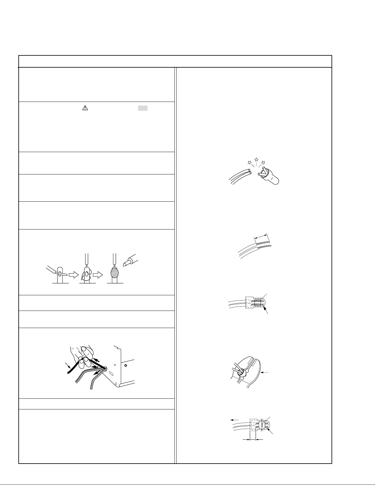
symbol and shaded ( ) parts are
12. Crimp type wire connector
In such cases as when replacing the power transformer in sets
where the connections between the power cord and power
transformer primary lead wires are performed using crimp type
connectors, if replacing the connectors is unavoidable, in order to prevent safety hazards, perform carefully and precisely
according to the following steps.
1) Connector part number : E03830-001
2) Required tool : Connector crimping tool of the proper type
which will not damage insulated parts.
3) Replacement procedure
(1) Remove the old connector by cutting the wires at a point
close to the connector.
Important : Do not reuse a connector (discard it).
cut close to connector
Fig.3
(2) Strip about 15 mm of the insulation from the ends of
the wires. If the wires are stranded, twist the strands to
avoid frayed conductors.
15 mm
Fig.1
7. Observe that wires do not contact heat producing parts
(heatsinks, oxide metal film resistors, fusible resistors, etc.)
8. Check that replaced wires do not contact sharp edged or
pointed parts.
9. When a power cord has been replaced, check that 10-15 kg of
force in any direction will not loosen it.
Power cord
Fig.2
10. Also check areas surrounding repaired locations.
11. Products using cathode ray tubes (CRTs)
In regard to such products, the cathode ray tubes themselves,
the high voltage circuits, and related circuits are specified for
compliance with recognized codes pertaining to X-ray emission.
Consequently, when servicing these products, replace the cathode ray tubes and other parts with only the specified parts.
Under no circumstances attempt to modify these circuits.
Unauthorized modification can increase the high voltage value
and cause X-ray emission from the cathode ray tube.
Fig.4
(3) Align the lengths of the wires to be connected. Insert
the wires fully into the connector.
Metal sleeve
Connector
Fig.5
(4) As shown in Fig.6, use the crimping tool to crimp the
metal sleeve at the center position. Be sure to crimp fully
to the complete closure of the tool.
1.25
2.0
5.5
Fig.6
(5) Check the four points noted in Fig.7.
Not easily pulled free
Wire insulation recessed
more than 4 mm
Fig.7
Crimping tool
Crimped at approx. center
of metal sleeve
Conductors extended
1
S40888-01
Page 4
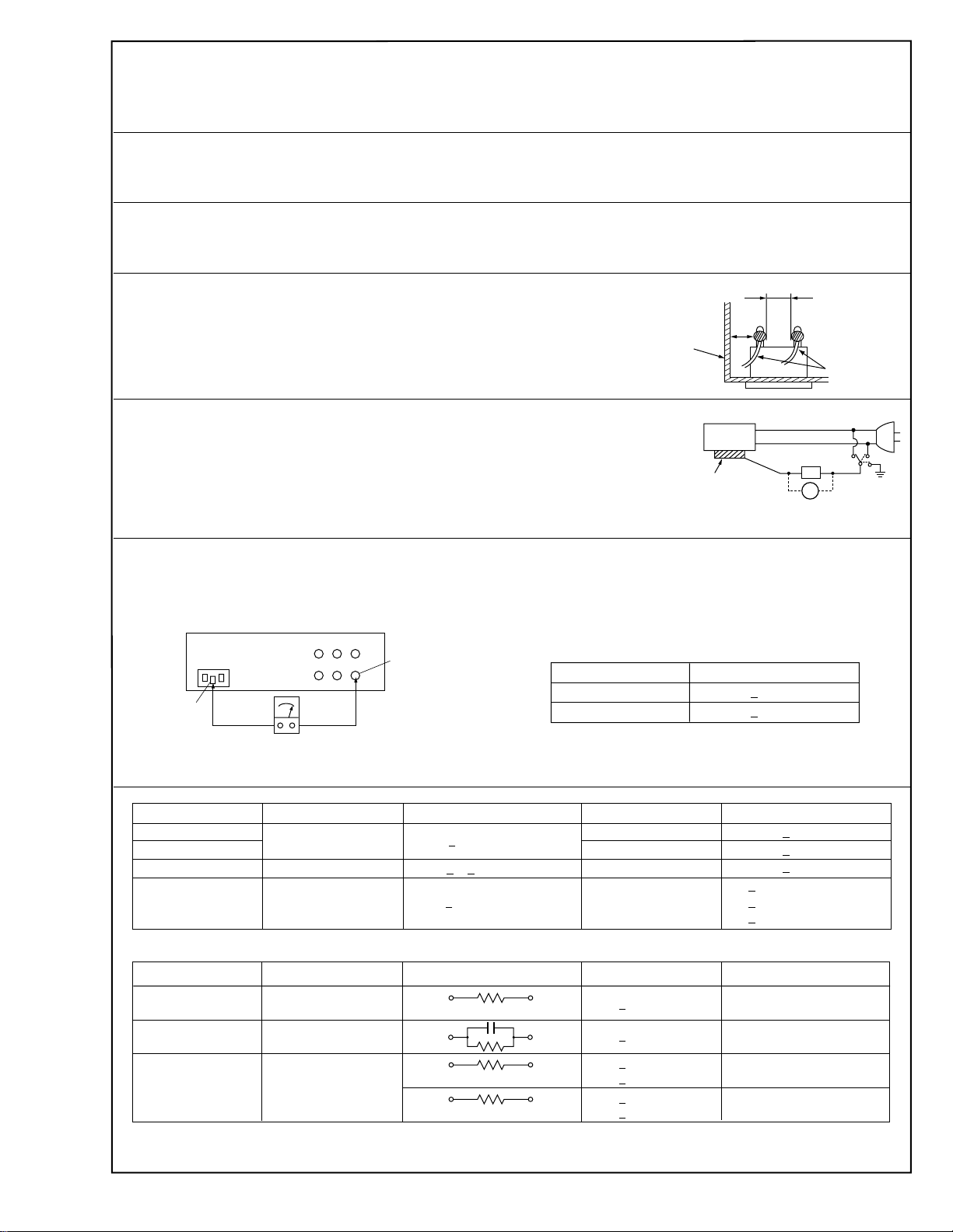
Safety Check after Servicing
Examine the area surrounding the repaired location for damage or deterioration. Observe that screws, parts and wires have been
returned to original positions, Afterwards, perform the following tests and confirm the specified values in order to verify compliance with safety standards.
1. Insulation resistance test
Confirm the specified insulation resistance or greater between power cord plug prongs and
externally exposed parts of the set (RF terminals, antenna terminals, video and audio input
and output terminals, microphone jacks, earphone jacks, etc.). See table 1 below.
2. Dielectric strength test
Confirm specified dielectric strength or greater between power cord plug prongs and exposed
accessible parts of the set (RF terminals, antenna terminals, video and audio input and output
terminals, microphone jacks, earphone jacks, etc.). See table 1 below.
3. Clearance distance
When replacing primary circuit components, confirm specified clearance distance (d), (d’) between soldered terminals, and between terminals and surrounding metallic parts. See table 1
below.
4. Leakage current test
Confirm specified or lower leakage current between earth ground/power cord plug prongs
and externally exposed accessible parts (RF terminals, antenna terminals, video and audio
input and output terminals, microphone jacks, earphone jacks, etc.).
Measuring Method : (Power ON)
Insert load Z between earth ground/power cord plug prongs and externally exposed accessible parts. Use an AC voltmeter to measure across both terminals of load Z. See figure 9 and
following table 2.
5. Grounding (Class 1 model only)
Confirm specified or lower grounding impedance between earth pin in AC inlet and externally exposed accessible parts (Video in,
Video out, Audio in, Audio out or Fixing screw etc.).
Measuring Method:
Connect milli ohm meter between earth pin in AC inlet and exposed accessible parts. See figure 10 and grounding specifications.
AC inlet
Earth pin
Exposed accessible part
Grounding Specifications
Region
USA & Canada
Europe & Australia
Chassis
Fig. 8
Externally
exposed
accessible part
Grounding Impedance (Z)
d
d'
Fig. 9
≤
Z 0.1 ohm
≤
Z 0.5 ohm
Power cord,
primary wire
ab
Z
V
c
Milli ohm meter
Fig. 10
AC Line Voltage
100 V
100 to 240 V
110 to 130 V
110 to 130 V
200 to 240 V
100 V
110 to 130 V
110 to 130 V
220 to 240 V
Note: These tables are unofficial and for reference only. Be sure to confirm the precise values for your particular country and locality.
Region
Japan
USA & Canada
Europe & Australia R 10 MΩ/500 V DC
Region Load Z
Japan
USA & Canada
Europe & Australia
Table 2 Leakage current specifications for each region
Insulation Resistance (R)
≤
R 1 MΩ/500 V DC
≥≥
1 MΩ R 12 MΩ/500 V DC
≤
Table 1 Specifications for each region
1 kΩ
0.15 µF
1.5 kΩ
2 kΩ
50 kΩ
Dielectric Strength
AC 1 kV 1 minute
AC 1.5 kV 1 miute
AC 1 kV 1 minute
AC 3 kV 1 minute
AC 1.5 kV 1 minute
i 1 mA rms Exposed accessible parts
i 0.5 mA rms
i 0.7 mA peak
i 2 mA dc
i 0.7 mA peak
i 2 mA dc
2
≤
≤
≤
≤
≤
≤
(Class 2)
(Class 1)
Clearance Distance (d), (d')
≤
d, d' 3 mm
≤
d, d' 4 mm
≤
d, d' 3.2 mm
≤
d 4 mm
≤
d' 8 mm (Power cord)
≤
d' 6 mm (Primary wire)
a, b, cLeakage Current (i)AC Line Voltage
Exposed accessible parts
Antenna earth terminals
Other terminals
S40888-01
Page 5
SECTION 1
Connector
Flat wire
Connector
DISASSEMBLY
1.1 BEFORE ASSEMBLY AND DISASSEMBLY
1.1.1 Precautions
1. Be sure to remove the power supply unit prior to mounting and soldering of parts.
2. When removing a component part that needs to disconnect
the connector and to remove the screw for removing itself,
first disconnect the connecting wire from the connector and
then remove the screw beforehand.
3. When connecting and disconnecting the connectors, be
careful not to damage the wire.
4. Carefully remove and handle the part to which some
spacer or shield is attached for reinforcement or
insulation.
5. When replacing chip parts (especially IC parts), desolder
completely first (to prevent peeling of the pattern).
6. Tighten screws properly during the procedures.
Unless specified otherwise, tighten screws at a torque
of 0.078N·m (0.8kgf·cm).
1.1.2 Assembly and disassembly
STEP
No.
1
2
PART Fig No. POINT NOTE
DECK OPE ASSY Fig.1-3-1 2(S1), (L1)–
✩CN A
FRONT COVER (S2a), (S2b), 2(S2c), (S2d) –
ASSY (S2e), (S2f), (L2)
✩CN B
▲▲ ▲▲ ▲
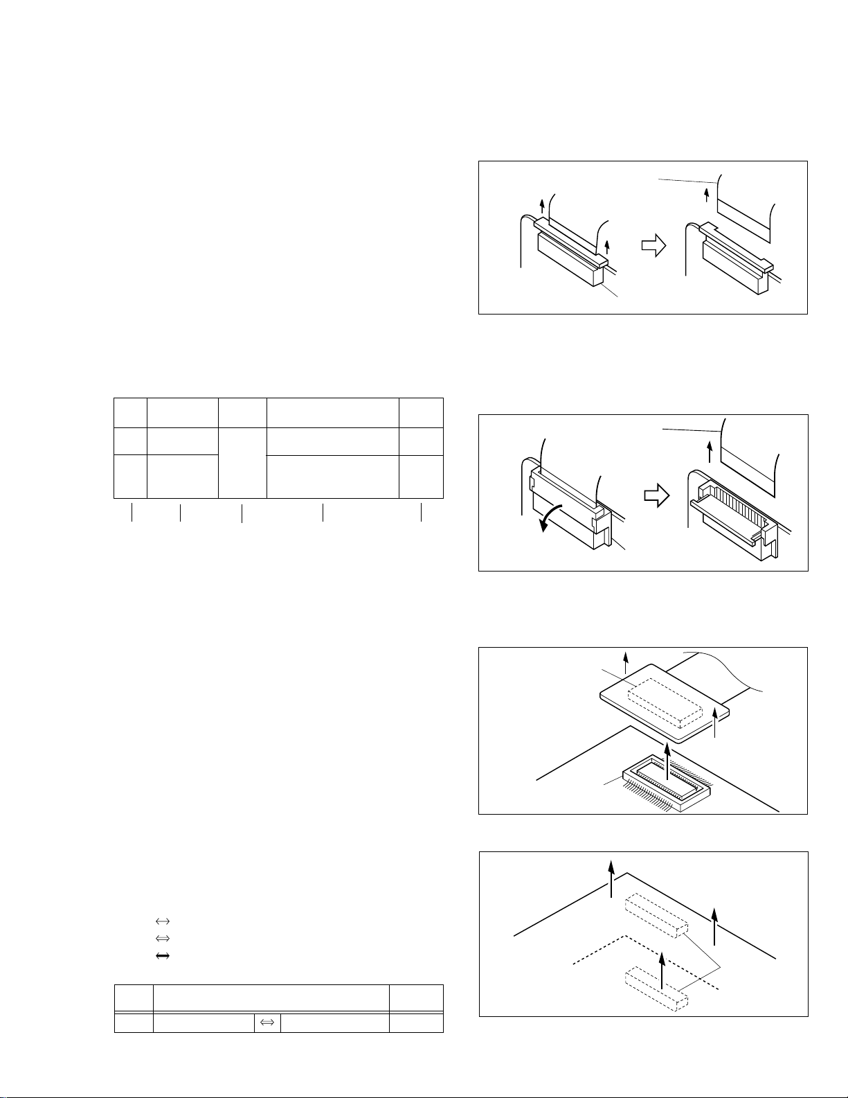
1.1.4 Disconnection of Connectors (Wires)
Connector
Pull both ends of the connector in the arrow direction, remove the lock and disconnect the flat wire.
Flat wire
Connector
Fig. 1-1-1 Connector 1
Extend the locks in the direction of the arrow for unlocking
and then pull out the wire. After removing the wire, immediately restore the locks to their original positions because the
locks are apt to come off the connector.
(1) (2) (3) (4) (5)
(1) Indicate the disassembly steps. When assembling, per-
form in the reverse order of these steps. This number
corresponds to the number in the disassembly diagram.
(2) Indicates the name of disassembly/assembly parts.
(3) Indicates the number in the disassembly diagram.
(4) Indicates parts and points such as screws, washers,
springs which must be removed during disassembly/
assembly.
Symbol Name, Point
S Screw
L Lock, Pawl, Hook
SD Soldering
聽
(Others) Connector, Cover, Bracket, etc.
(Example)
• 2 (S1): Remove the two screws (S1) for removing the
part 1.
• CN A : Disconnect the connector A.
• SD1 : Unsolder at the point SD1.
(5) Precautions on disassembly/assembly.
1.1.3 Destination of connectors
Note:
Three kinds of double-arrows in connection tables respectively show kinds of connector/wires.
: Wire
: Flat wire
: Board to Board connector
[Example]
CONN.
No.
A DECK OPE ASSY – AUDIO VF CN803 6
CONNECTOR Pin No.
Fig. 1-1-2 Connector 2
B-B connector
Pull the board by both the sides in the direction of the arrow for disconnecting the B-B connector
Connector
Connector
Fig. 1-1-3 Connector 3
Fig. 1-1-4 Connector 4
1-1
Page 6
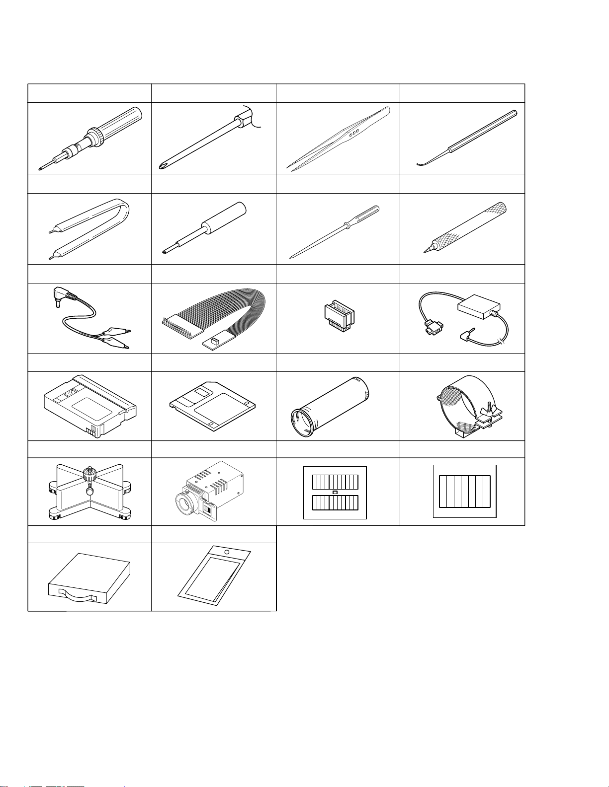
1.2 JIGS AND TOOLS REQUIRED FOR DISASSEMBLY, ASSEMBLY AND ADJUSTMENT
1.2.1 Tools required for adjustments
1
5
9
13 14 15
Torque Driver
YTU94088
Connector Extractor
YTU94036A
Power Supply Jig
YTU94060A
Alignment Tape
MC-2
23
6
10
Bit
YTU94088-003
Guide Driver
YTU94148A
Jig Connector Cable
YTU93091B
Service Support System
YTU94057-48
11 12
Tweezers
P-895
Adjustment Driver
78
YTU94028
Extension connector
YTU94145A
INF Adjustment Lens
YTU92001B
Chip IC Replacement Jig
4
16
PTS40844-2
Slit Washer Installation Jig
YTU94121A
PC Cable
QAM0099-002
INF Adjustment Lens Holder
YTU94087
17
21 22
Camera Stand
YTU93079
Soldering Kit
YTU96016C
Light box Assembly
18
YTU93096A
Cleaning Cloth
KSMM-01
1. Torque driver
Be sure to use to fastening the mechanism and exterior
parts because those parts must strictly be controlled for
tightening torque.
2. Bit
This bit is slightly longer than those set in conventional
torque drivers.
3. Tweezers
To be used for removing and installing parts and wires.
19 20
Gray Scale Chart
YTU94133A
Table 1-2-1
4. Chip IC replacement jig
To be used for adjustment of the camera system.
5. Connector extractor
To be used to release the connector.
6. Guide driver
To be used to turn the guide roller to adjustment of the
linarity of playback envelope.
7. Adjustment driver
To be used for adjustment.
Color Bar Chart
YTU94133C
1-2
Page 7
8. Slit washer installation jig
To be used to install slit washers.
9. Power supply jig
To be used for power supply to the set when the
exclusive DC power cord is not used. Carefully use
this jig, especially not to damage the battery terminal
(+/-).
10. Jig connector cable
Connected to CN1010 of the main board and used
for electrical adjustment, etc.
11. Extension connector
Connect this extension connector to the connector
of the jig connector cable for extending the cable
connector.
Note:
For supplying the power through the coupler
by removing the cover (for jig), use this
extension connector double for connecting
the jig connector cable.
12. PC cable
To be used to connect the VideoMovie and a
personal computer with each other when a personal
computer is used for adjustment.
13. Alignment tape
To be used for check and adjustment of
interchangeability of the mechanism.
14. Service support system
To be used for adjustment with a personal computer.
15. INF adjustment lens
To be used for adjustment of the camera system.
16. INF adjustment lens holder
To be used together with the camera stand for
operating the VideoMovie in the stripped-down
condition such as the status without the exterior
parts or for using commodities that are not yet
conformable to the interchangeable ring.
17. Camera stand
To be used together with the INF adjustment lens
holder.
18. Light box assembly
To be used for adjustment of the camera system.
19. Gray scale chart (for Light box assembly)
To be used for adjustment of the camera system.
20. Color bar chart (for Light box assembly)
To be used for adjustment of the camera system.
21. Soldering kit
Thin head is made so that it can be inserted into
small spaces.
22. Cleaning cloth
Recommended cleaning cloth to wipe down the
video heads, mechanism (tape transport system),
optical lens surface.
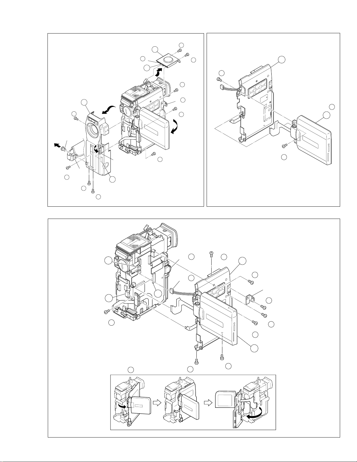
1.3 DISASSEMBLY/ASSEMBLY OF CABINET PARTS AND BOARD ASSEMBLY
1.3.1 Disassembly flow chart
This flowchart indicates the disassembly step for the cabinet parts and board assembly in order to gain access to
item(s) to be serviced. When reassembling, perform the
step(s) in reverse order.
1 DECK OPE ASSY
2 FRONT COVER ASSY
3 UPPER CASE ASSY
(INC. MONITOR, etc.)
4 MONITOR ASSY
5 BASE ASSY
6 LOWER CASE ASSY
(INC. OP BLOCK, E. VF)
7 OP BLOCK ASSY
8 STROBE ASSY
9 MIC
0 E VF ASSY
- AUDIO VF BOARD ASSY
= MDA BOARD ASSY
~ MAIN BOARD ASSY
!
MECHANISM ASSY
1-3
Page 8
1.3.2 Disassembly method (I)
STEP
No.
1
2
3
4
5
6
7
8
9
PART Fig No. POINT NOTE
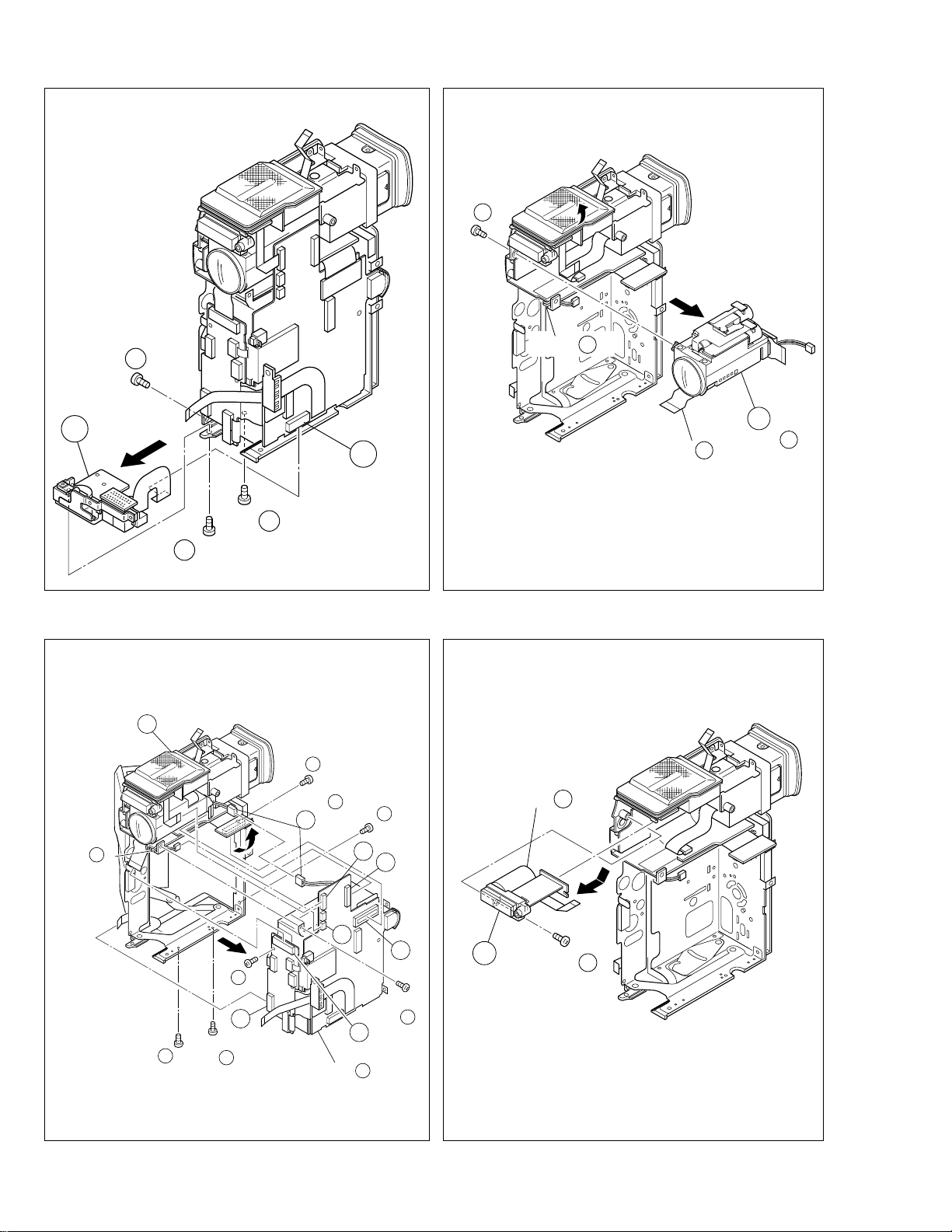
DECK OPE ASSY Fig.1-3-1 2(S1), (L1) –
✩CN A
FRONT COVER (S2a), (S2b), 2(S2c), (S2d) –
ASSY (S2e), (S2f), (L2)
COVER (DV), STUD (HOOK)
✩CN B
U. CASE ASSY Fig. 1-3-2a 2(S3a), (S3b), 2(S3c), 3(S3d) NOTE3a
(Inc. MONITOR LOCK (MONITOR) NOTE3b
ASSY) ✩CN C, D, E
(CN C : DVX9,10 ONLY)
MONITOR ASSY Fig. 1-3-2b (S4a), (S4b) NOTE4
BASE ASSY Fig. 1-3-3 (S5a), (S5b), (S5c) –
✩CN F
L. CASE ASSY Fig. 1-3-4 6(S6) NOTE6a
✩CN G, H, J, K, L, M, N NOTE6b
(CN G, K : DVX9,10 ONLY) NOTE6c
OP BLOCK ASSY Fig. 1-3-5 (S7) NOTE7a
STROBE ASSY Fig. 1-3-6 (S8) NOTE8
(DVX9,10 ONLY)
MIC Fig. 1-3-7 (L9) NOTE9
✩CN O
NOTE7b
CONN.
No.
A DECK OPE ASSY – AUDIO VF CN803 6
B JACK CN901 MAIN CN1008 16
C MDA CN207 SUB OPE ASSY – 7
D MAIN CN1004 W/B SENS – 3
E MAIN CN1007 MONITOR CN7501 45/39
F MAIN CN1014 MULTI PIN – 33
G MDA CN208 MMC CN601 14
H MDA CN205 OP BLOCK ASSY – 24
J MAIN CN1009 EJECT SW – 2
K MAIN CN1011 STROBE CN6501 12
L MAIN CN1003 CCD – 20
M MAIN CN1016 AUDIO VF CN801 100
N MAIN CN1017 CCD CN5203 2
O AUDIO VF CN804 MIC – 5
P VF BL CN501 AUDIO VF CN805 20
Q AUDIO VF CN802 CAMERA OPE UNIT – 12
R MAIN CN1002 MDA CN206 80
S MDA CN202 DRUM MOTOR – 11
T MDA CN201 LOADING MOTOTR – 6
U MDA CN203 CAPSTAN MOTOR – 18
V MDA CN204 SENSOR – 15
W MAIN CN1005 ROTARY ENCODER – 6
X MAIN CN1001 HEAD – 8
CONNECTOR Pin No.
Table 1-3-3
0
E VF ASSY Fig. 1-3-8 (S0a), (S0b), (S0c), 2(L0a) NOTE0a
-
AUDIO VF Fig. 1-3-9 2(S-a), (S-b), 2(L-) –
BOARD ASSY ✩CN Q
=
MDA BOARD Fig. 1-3-10 (S=) NOTE=a
ASSY ✩CN R, S, T, U, V NOTE=b
~
MAIN BOARD (S~a), (S~b), (L~) NOTE~
ASSY SHIELD PLATE
!
MECHANISM 2(S!a), (S!b), 2(L!) –
ASSY BRACKET (MECHA)
(L0b), BRACKET (TOP) NOTE0b
✩CN P NOTE0c
✩CN W, X
Table 1-3-2
Note3a:
Note3b:
Note4:
Note6a:
Note6b:
Note6c:
Note7a:
Note7b:
Note8:
Note9:
Note0a:
Note0b:
Note0c:
Note=a:
Note=b:
Note~:
When removing, be careful not to break the wire.
When removing, be careful not to damage any part.
On removing, slightly open the front side so as to
shift it from the frame.
For disassembling method, refer to Fig. 1-4-1.
When removing, be careful not to break the wire.
Remove the board assembly (MAIN/MDA) and
mechanism assembly together.
When installing, arrange the wire between the OP
block assembly and VF assembly.
When removing, be careful neither to break the wire
nor to damage any part.
For disassembling method, refer to Fig. 1-6-1.
Be careful not to get an electric shock during the
work.
When reassembling, carefully arrange the wire.
When disassembling/reassembling, be careful not
to damage any part.
When reassembling, set the bracket (top) as the VF
unit is pulled out, and secure the installation in order
0
a) and (L0b).
of (L
For disassembling method, refer to Fig. 1-5-1.
When disconnecting the connector, carefully handle
the FPC on the top of the connector.
Disconnect the connector V last, because it is
positioned inside.
When reassembling, carefully locate the FPC so
that it is sandwiched between the mechanism
assembly and MAIN board assembly.
1-4
Page 9
(S b)
STUD
(HOOK)
1
1
1
1
(L )
A
2
4
2
(S )
✽
5
2
(S c)
2
(L )
✽
6
2
(S c)
2
1
(S )
18
4
(S a)
3
4
NOTE
4
3
2
(S a)
HOOK
✽✽
9
2
(S f)
8
2
(S e)
COVER
B
Fig. 1-3-1
D
C
17
3
(S d)
✽
7
2
(S d)
(DV)
✽ 0.118N·m (1.2kgf·cm)
✽✽ 0.098N·m (1.0kgf·cm)
E
NOTE b
NOTE a
3
3
✽
10
3
(S a)
(S b)
Fig. 1-3-2b
✽ 0.118N·m (1.2kgf·cm)
3
✽
11
3
(S a)
LOCK
(MONITOR)
12
3
(S b)
13
3
(S c)
14
3
(S c)
19
4
NOTE b
3
16
3
(S d)
Fig. 1-3-2a
15
3
(S d)
4
1-5
Page 10
✽
29
7
(S )
5
20
5
(S a)
(S b)
6
21
5
(S c)
Fig. 1-3-3
22
5
25
6
(S )
NOTE a
7
7
NOTE b
F
✽ 0.118N·m (1.2kgf·cm)
NOTE a
Fig. 1-3-5
7
7
NOTE a
1-6
NOTE c
N
6
23
6
(S )
G
28
6
(S )
27
6
(S )
Fig. 1-3-4 Fig. 1-3-6
NOTE b
J
(S )
K
H
6
6
L
M
24
(S )
6
26
6
NOTE
8
✽ 0.098N·m (1.0kgf·cm)
8
✽
30
8
(S )
Page 11
NOTE
W
13
12
S
T
U
R
V
W
14
X
(S a)
40
BRACKET
(MECHA)
14
(S b)
39
13
(S b)
42
NOTE 12 b
NOTE 13
14
NOTE a
12
(S a)
41
14
(S a)
38
13
(S )
37
12
(L )
14
(L )
13
SHIELD
PLATE
X
9
9
(L )
✽
35
11
9
(S a)
11
(L )
✽
34
11
Q
(S a)
NOTE
10
(L b)
P
9
31
10
(S a)
✽
NOTE a
O
✽ 0.098N·m (1.0kgf·cm)
Fig. 1-3-7 Fig. 1-3-9
✽ 0.098N·m (1.0kgf·cm)
BRACKET
10
(TOP)
(S b)
10
(L a)
✽
32
10
10
NOTE c
10
✽✽
✽
36
11
(S b)
11
10
NOTE b
10
BRACKET
(TOP)
10
(L
a)
10
(L b)
Fig. 1-3-8 Fig. 1-3-10
FPC
✽
33
10
(S c)
1-7
Page 12
1.4 DISASSEMBLY OF 4 MONITOR ASSEMBLY
1.4.1 4 Monitor assembly/Hinge assembly
1. Remove the four screws (1-4). While opening the monitor
cover assembly as shown by the arrow, release the two
hooks (L4a, L4b) from engagement and remove the
monitor cover assembly.
2. Remove the parts out of the monitor case assembly and
unlock the connector Y. While raising the hinge assembly
upwards, get the two hooks (L4c, L4d) disengaged and
disconnect the FPC by pulling it out. Then, remove the
hinge assembly.
Note4a:
When removing the parts out of the monitor case
assembly, be very careful not to damage the FPC
and parts.
3. Disconnect FPC from the connector Z and then remove
the MONITOR board assembly and backlight.
Note4b:
Remove the MONITOR board assembly and
backlight together unless it is needed to separate
them from each other for part replacement, etc.,
because the two are soldered to each other.
4. Remove the LCD module.
1.4.2 Hinge assembly
1. Remove the two screws (5, 6). While releasing the two
hooks (L4f, L4g) from engagement, remove the hinge
cover (U).
Note4c:
Be careful not to lose any part during the abovementioned process.
2. Draw the FPC assembly out of the hinge cover (L) and
then remove the FPC assembly from the hinge assembly.
Note4d:
When reassembling, wind the FPC assembly
around the hinge assembly by three turns and a
half.
Be careful not to break the FPC wire during the
work.
4
NOTE d
FPC ASSY
HINGE
ASSY
4
(L g)
NOTE a
4
(L c)
HINGE
ASSY
5
4
(S f)
(L f)
HINGE
COVER(U)
4
4
6
4
(S f)
NOTE c
MAGNET
FPC ASSY
NOTE
HINGE
COVER(L)
4
4
(L d)
MONITOR
COVER ASSY
4
(L a)
1
4
(S c)
2
4
(S c)
4
4
d
NOTE b
4
(L b)
Y
Z
4
4
(S e)
3
4
(S d)
MONITOR
BOARD
ASSY
4
(L e)
BACK
LIGHT
LCD
MODULE
1-8
Fig. 1-4-1
4
NOTE a
✽ : 0.098N·m (1.0kgf·cm)
Page 13
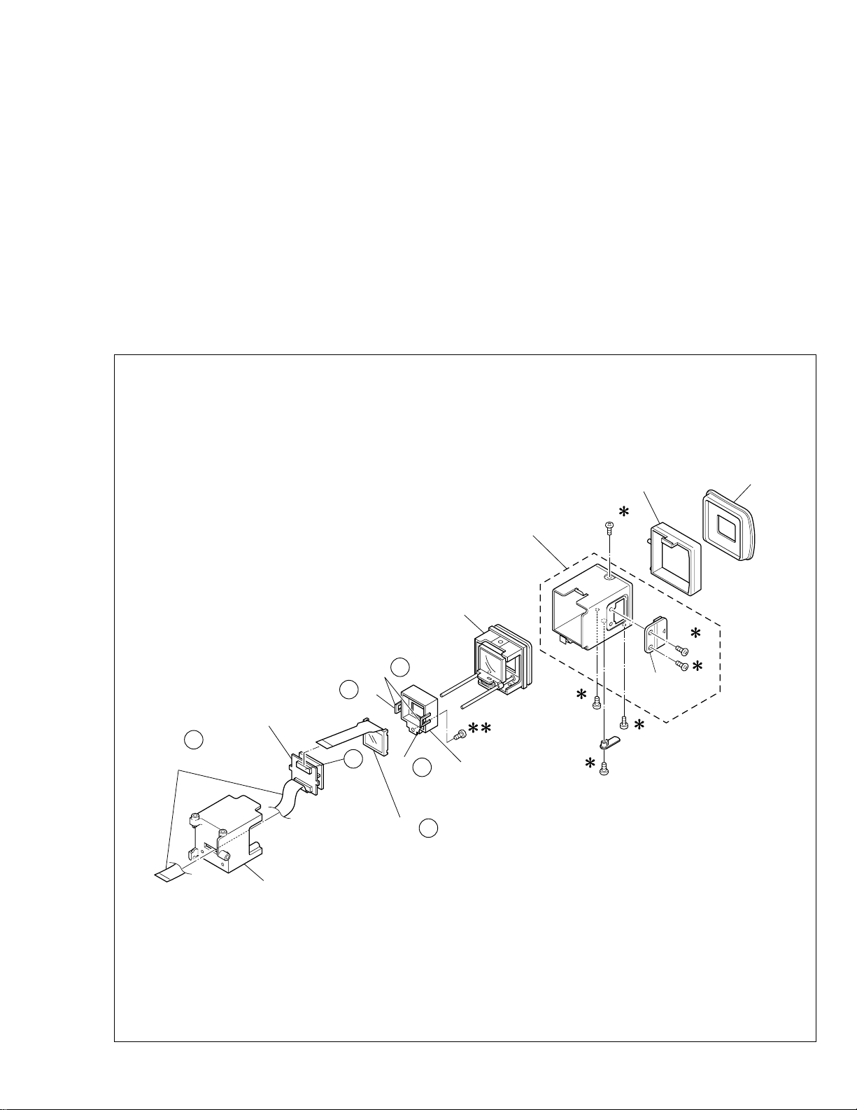
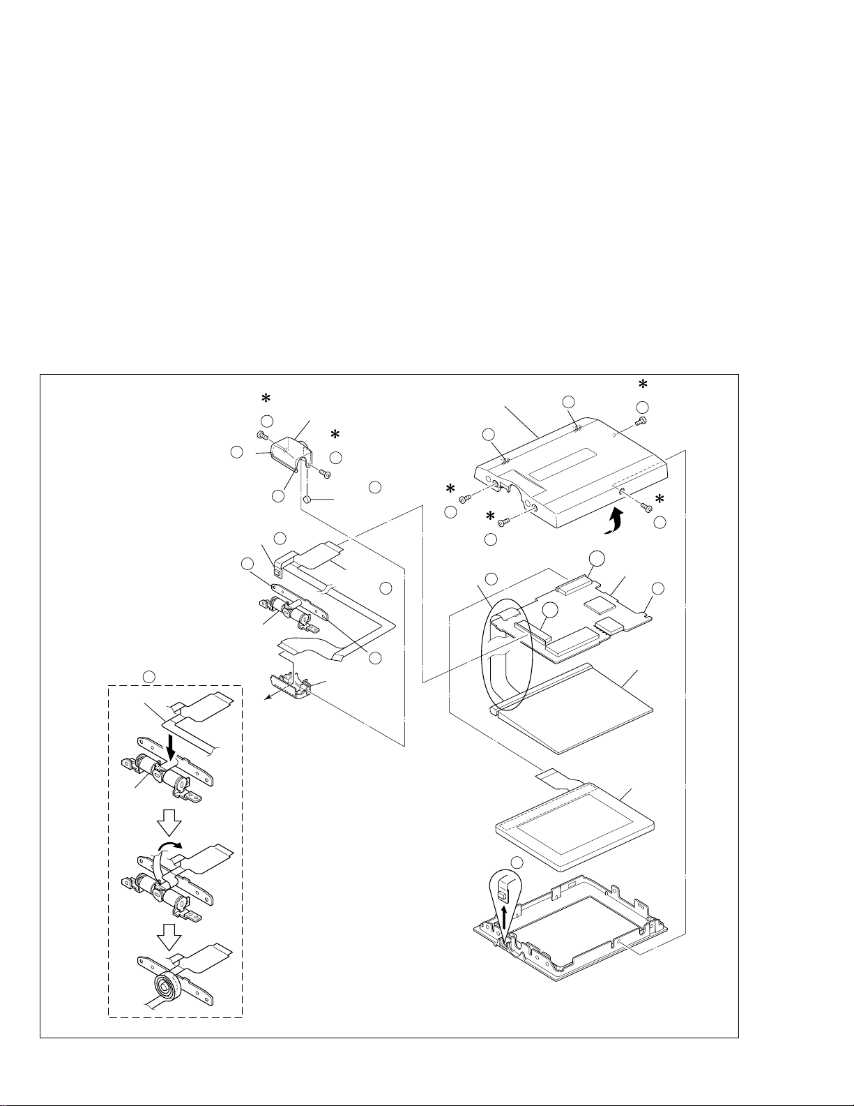
1.5 DISASSEMBLY OF 0 E VF ASSEMBLY
1.5.1 0E VF assembly
Note5a:
Note5b:
Note5c:
1. Remove the eyecup and pull out the guide (VF).
2. Draw the frame (VF) out of the case assembly.
<Case assembly>
3. Remove the screw (1) first and then lever (VF).
4. Remove the three screws (2-4) and draw out the eyepiece
When disassembling the E VF assembly, remove
the frame (VF) from the case assembly depending
on the situation.
Be very careful not to get the inside of the VF soiled
or dusty during and after disassembling the E VF
assembly.
After the screw having the loose-proof tip was once
removed from the E VF assembly, don’t reuse it.
sub assembly.
<Frame (VF)>
5. Remove the screw (5) first and then LCD module/holder
(LCD).
Note5d:
6. Get the two hooks (L5a, L5b) disengaged and then
Note5e:
7. Disconnect the connector (a) and remove the LCD module.
Note5f:
Pay heed to the FFC not to damage it during the
removing work.
remove the holder (LCD).
Carefully proceed with the above-mentioned work
not to damage any part.
Pay heed the parts not to damage any thing.
B/L SUB ASSY
NOTE d
5
FFC
EYE PIECE
SUB ASSY
NOTE e
5
(L a)
a
5
(L b)
NOTE f
LCD MODULE
EYE CUP
CASE/CAP
GUIDE(VF)
2
6
CAP
3
5
5
HOLDER
(LCD)
1
5
(VF)
4
7
FRAME(VF)
✽ : 0.069N·m (0.7kgf·cm)
✽✽ : 0.098N·m (1.0kgf·cm)
Fig. 1-5-1
1-9
Page 14

1.6 DISASSEMBLY OF 7 OP BLOCK ASSEMBLY/CCD BOARD ASSEMBLY
1.6.1 Precautions
1. Carefully handle the CCD image sensor, optical LPF, lens,
etc. during the disassembly work. Pay the most careful
attention to the surface of those parts not to get it soiled,
scratched or dusty. If some of those surfaces gets soiled
with fingerprints, etc., wipe it out with silicone paper, clean
chamois, cleaning cloth or the like.
2. The new CCD image sensor is occasionally shipped from
the factory as a protection seal is applied onto its
transparent glass. If so, leave the protection seal as it is
and remove it just before installing the CCD image sensor
in the OP block assembly.
1.6.2 How to remove OP block assembly and CCD board
assembly
1. Unsolder at the two points (SD1) and remove the shield
case.
2. Unsolder at the sixteen points (SD2) and remove the CCD
board assembly.
3. Remove the two screws (1, 2) and then remove the CCD
base assembly.
Note6a:
Note6b:
Carefully remove the CCD base assembly, because
the space rubber and optical LPF may be removed
together with the CCD image sensor.
When replacing the CCD image sensor, don’t
replace it individually but replace the CCD base
assembly in whole with a new one.
1.6.3 How to install OP block assembly and CCD board
assembly
1. Install the optical LPF with the space rubber fitted to its
CCD side in the OP block assembly.
2. Paying heed to the space rubber not to get it to come off
the setting position, install the CCD base assembly in
place and fasten it together with the space rubber with the
two screws (1, 2).
3. Set the CCD board assembly in the CCD base assembly,
and fasten it by soldering at the fourteen points (SD2).
4. Install the shield case and fasten it by soldering at the two
points (SD1).
1.6.4 Replacement of service parts
Service parts to be supplied for the OP block assembly are as
follows.
When replacing a part, be very careful not to get the FPC wire
broken or damaged by soldering (overheating).
1. Focus motor
2. Zoom motor
3. Iris motor unit
Note6c:
Note6d:
When soldering the FPC wire of the focus motor or
zoom motor during the replacement work, be sure
to keep the tip of a soldering iron approximately 1
mm above the terminal.
The iris motor unit includes one FPC assembly and
two sensors.
✽ : 0.118N·m (1.2kgf·cm)
NOTE6c,d
IRIS MOTOR UNIT
✽
✽
35
OP BLOCK ASSEMBLY
✽
4
NOTE6c
FOCUS MOTOR
✽
✽
7
6
✽
8
OPTICAL LPF
BLUE
OP
SIDE
✽
CCD
SIDE
THIN
9
NOTE6a
OPTICAL LPF
NOTE6c
ZOOM MOTOR
THICK
✽
1
(SD1)
(SD2)
✽
2
CCD
NOTE6a
SHIELD CASE
CCD BOARD
ASSEMBLY
NOTE6a,b
BASE ASSEMBLY
SPACER
1-10
Fig. 1-6-1
Page 15

1.7 HOW TO TAKE OUT CASSETTE TAPE MANUALLY
1.7.1 How to remove cassette tape manually from the set
If the cassette tape is not ejected from the cassette housing
because of some electric trouble, it can be removed from the
set by the temporary measure that is to turn the loading motor
forcibly as mentioned below.
Through the removing work, pay heed to the exterior parts
such as the covers, etc. as well as to the cassette tape to get
nothing damaged.
<Procedure>
1. Disconnect the power supply (battery or DC cord) from
the set.
2. Dismantle the deck ope assy, front cover assembly
referring to the section 1 (page 1-4, 1-5).
Note:
When and after dismantling the front assembly, pay
careful attention to the internal components such as
the OP block assembly (lens), battery terminal, etc.
that are exposed after the front assembly is removed.
3. Open the cassette cover assembly completely and hold
it open through the work.
4. Supply 3 V DC to the terminals (electrodes) on the top
of the loading motor to slide the slide deck assembly
to the front side, and stop the power supply when both
the pole bases are positioned in the unloading status
inside the tape. Since the tape remains as it is not
wound up at that time, pay careful attention to the tape
not to damage it and not to soil it with grease, etc. If
unloading operation is continued after both the pole
bases return to their respective positions inside the tape,
the mechanism enters the eject mode and the cassette
housing assembly is lifted up. If it occures, the pulledout tape may be caught in the cassette lid and the tape
may be resultingly damaged.
5. Turn the center gear assembly with a sharp-pointed thing
(chip IC replacing jig, etc.) in the direction of the arrow
to wind up the tape. Carefully turn the center gear assembly not to damage the tape.
If the tape cannot be wound up by turning the center gear
assembly, it is thinkable that the idler arm assembly is
positioned not to engage with the reel disk assembly. If
so, shift the mechanism mode so that the idler arm
assembly is correctly engaged with the reel disk assembly. After fine adjusting the engagement, try to wond up
the tape is the same manner once more.
In such the event, it is recommended to shift the idler
arm assembly slightly in the loading direction.
6. After confirming that the tape is completely wound up,
proceed with unloading operation until the mechanism
enters the eject mode. Then, take the cassette tape out
of the cassette housing.
7. After removing the cassette tape, check to see if the
manually wound part of the tape is not soiled with grease,
etc. At the same time, check the mechanism assembly,
particularly the tape transport system, whether there is
something abnormal or not.
(DC3V)
DRUM
REEL DISK
(SUP)
1
REEL DISK
CAPSTAN
MOTOR
2
3
4
(TU)
Fig. 1-7-1
1-11
Page 16
1.8 SERVICE NOTE
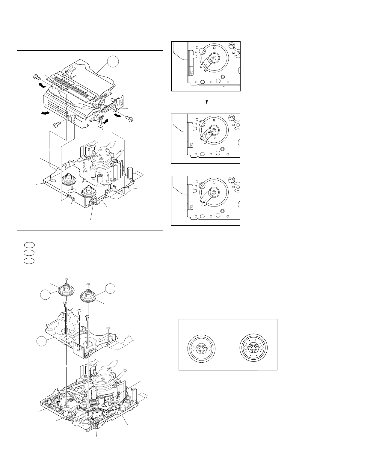
1 2 3 4 5 6 7 8 9 10 11 12 13 14 15 16 17 18 19 20 21 22
1
2
345
✻✻✻✻
✻ ✻
Fig. 1-3-1 Fig. 1-3-2a Fig. 1-3-2b Fig. 1-3-3
I IIII I IIIIII IIVIII II IIII II
23 24 25 26 27 28 29 30 – 31 32 33 34 35 36 37 38 39
8
7
4
MONITOR ASSY
6
!
09-=~
Fig. 1-3-4
Fig. 1-3-5 Fig. 1-3-6 Fig. 1-3-7 Fig. 1-3-8 Fig. 1-3-9 Fig. 1-3-10
I
Fig. 1-3-10
I
IIII III
Fig. 1-4-1
III
IIIII
Symbol No.
Removing order of screw
Place to stick screw
Reference drawing
Screw tightening torque
→
→
→
→
→
Symbol No.
Removing order of screw
Place to stick screw
Reference drawing
Screw tightening torque
→
→
→
→
→
Symbol No.
Removing order of screw
Place to stick screw
Reference drawing
Screw tightening torque
→
→
→
→
→
Removing order of screw
Place to stick screw
Reference drawing
Screw tightening torque
→
→
→
→
Removing order of screw
Place to stick screw
Reference drawing
Screw tightening torque
→
→
→
→
Removing order of screw
Place to stick screw
Reference drawing
Screw tightening torque
→
→
→
→
–
40 41 42
123456
1234567
0
E VF ASSY
V V V V III V V
7
OP BLOCK ASSY
Fig. 1-6-1
II
123456789
< NOTE >
1) ✻ : Dont’t reuse the screw, because screw lock bond was applied to them.
2) Pay careful attention to tightening torque for each screw.
I : 0.078N·m (0.8kgf·cm) II : 0.118N·m (1.2kgf·cm) III : 0.098N·m (1.0kgf·cm)
IV : 0.198N·m (2.0kgf·cm) V : 0.069N·m (0.7kgf·cm)
Fig. 1-5-1
Table 1-8-1
1-12
Page 17

1.9 EMERGENCY DISPLAY
Whenever some abnormal signal is input to the syscon CPU,
an error number (E01, as an example) is displayed on the
LCD monitor or (in the electronic view finder).
In every error status, such the message as shown below
alternately appear over and over.
• In an emergency mode, all operations except turning on/
off the POWER switch are ineffectual.
LCD
display
E01 LOADING
E02 UNLOADING
E03 TU & SUP REEL
Emergency
mode
FG
Details
In the case the encoder position is not shifted
to the next point though the loading motor has
rotated in the loading direction for 4 seconds
or more. This error is defined as [E01].
In the case the encoder position is not shifted
to the next point though the loading motor has
rotated in the unloading direction for 4 seconds
or more. This error is defined as [E02].
In the case no REEL FG is produced for 4 seconds or more in the capstan rotation mode after loading was complete, the mechanism mode
is shifted to STOP with the pinch roller set off.
This error is defined as [E03].
However, no REEL EMG is detected in the
SLOW/STILL mode.
Example (in case of the error number E01):
E01
UNIT IN
SAFEGUARD MODE
E01
REMOVE AND
REATTACH BATTERY
Possible cause
1. The mechanism is locked during mode shift.
2. The mechanism is locked at the mechanism loading
end, because the encoder position is skipped during
mechanism mode shift.
3. No power is supplied to the loading MDA.
1. The mechanism is locked during mode shift.
2. The mechanism is locked at the mechanism loading
end, because the encoder position is skipped during
mechanism mode shift.
1. The idler gear does not engage with the reel disk well.
2. Though the idler gear and reel disk are engaged with
each other, the tape is not wound because of overload to the mechanism.
3. No FG pulse is output from the reel sensor.
4. No power is supplied to the reel sensor.
5. Tape transport operation takes place with a cassette
having no tape inside.
6. The tape slackens and no pulse is produced until the
slack is taken up and the tape comes into the normal
status.
E04 DRUM FG
E05 –
E06 CAPSTAN FG
In the case there is no DRUM FG input in the
drum rotation mode for 4 seconds or more. This
error is defined as [E04], and the mechanism
mode is shifted to STOP with the pinch roller
set off.
1. The drum cannot be started or drum rotation is stopped
because tape transport load is too high.
1) Tape tension is extremely high.
2) The tape is damaged or soiled with grease, etc.
2. The DRUM FG signal is not received by the syscon
CPU.
1) Disconnection in the middle of the signal line.
2) Failure of the DRUM FG pulse generator (hall element).
3. No drum control voltage is supplied to the MDA.
4. No power is supplied to the DRUM MDA.
– –
In the case no CAPSTAN FG is produced in
the capstan rotation mode for 2 seconds or
more. This error is defined as [E06], and the
mechanism mode is shifted to STOP with the
pinch roller set off.
However, no CAPST AN EMG is detected in the
STILL/FF/REW mode.
1. The CAPSTAN FG signal is not received by the syscon
CPU.
1) Disconnection in the middle of the signal line.
2) Failure of the CAPSTAN FG pulse generator (MR
element).
2. No capstan control voltage is supplied to the MDA.
3. No power is supplied to the CAPSTAN MDA.
4. The capstan cannot be started or capstan rotation is
stopped because tape transport load is too high.
1) Tape tension is extremely high. (Mechanical lock-
ing)
2) The tape is damaged or soiled with grease, etc.
(Tape tangling occurs, etc.)
Table 1-9-1
(DVC_03)
1-13
Page 18

SECTION 2
MECHANISM ADJUSTMENT
2.1 PRELIMINARY REMARKS ON ADJUSTMENT AND REPAIR
2.1.1 Precautions
1. When fastening parts, pay careful attention to the tightening
torque of each screw. Unless otherwise specified, tighten a
screw with the torque of 0.039 N·m (0.4 kgf·cm).
2. Be sure to disconnect the set from the power supply before
fastening and soldering parts.
3. When disconnecting/connecting wires, be careful not to get
them and their connectors damaged. (Refer to the Section 1.)
4. When replacing parts, be very careful neither to damage other
parts nor to fit wrong parts by mistake.
2.1.2 Notes on procedure for disassemby/assembly
The disassembling procedure table (Table 2-2-2 on page
2-5, a part of the table is shown below for reference) shows
the procedure to disassemble/reassemble mechanism parts.
Carefully read the following explanation before starting actual disassembling/reassembling work. The item numbers
(circled numbers) in the following explanation correspond to
those appearing under respective columns of the table.
(1) Circled numbers appearing in this column indicate the
order to remove parts. When reassembling, follow these
numbers in the reverse order. Circled numbers in this
column correspond to those appearing in drawings of
this section.
(2) This column shows part names corresponding to circled
numbers in the left column.
(3) The symbol (T or B) appearing in this column shows the
side which the objective part is mounted on.
T = the upper side, B = the lower side
(4) Symbols appearing in this column indicate drawing
numbers.
(5) This column indicates parts and points such as screws,
washers, springs, and others to be removed/fitted for
disassembling/reassembling the mechanism. Besides
such the parts, this column occasionally indicates
working points.
P = Spring
W = Washer
S = Screw
* = Lock (L), soldering (SD), shield, connector (CN),
etc.
Example • Remove (W1) = Washer W1.
• * Remove the solder at (SD1) = Point SD1.
• * Disconnect A = Connector A .
(6) Numbers in this column represent the numbers of notes
in the text. For example, “1” means “Note 1”.
(For parts that need phase adjustment after reassembling, refer to “2.2.7 Check and adjustment of mechanism
phase”.)
(7) This column indicates required after-disassembling/-
reassembling work such as phase adjustment or
mechanism adjustment.
Step
Part Name
Fig.
Point
Note
Remarks
A Cassette housing assembly T Fig. 2-2-12 3(S1),(L1a)-(L1d) 1a, 1b, 1c, 1d Adjustment
2a
2b
2c
3a
5
(1) (2) (3) (4) (5) (6) (7)
2-1
Reel disk (SUP) assembly T Fig. 2-2-13 (W2) 2a, 2b
Reel disk (TU) assembly T Fig. 2-2-13 (W2) 2a, 2b
Reel cover assembly T Fig. 2-2-13 (S2b),2(S2a),(W2) 2c, 2d
Tension arm assembly T Fig. 2-2-14 (W3a) 3b
5
5
5
5 55
Page 19
2.2 DISASSEMBLY/ASSEMBLY OF MECHANISM
<SUB CAM GEAR>
TOP VIEW BOTTOM VIEW
ASSEMBLY
2.2.1 General statement
The mechanism should generally be disassembled/assembled in the EJECT mode (ASSEMBLY mode). (Refer to Fig.
2-2-1.)
However, when the mechanism is removed from the main body,
it is set in the STOP mode. Therefore, after the mechanism is
removed from the main body, supply 3 V DC to the electrode
on the top of the loading motor to enter the mechanism mode
into the EJECT mode compulsory.
<Mechanism assembly/Cassette housing assembly>
DC3V
<EJECT mode>
Fig. 2-2-2
Motor
<Back side of the mechanism assembly>
<C IN mode>
Fig. 2-2-3
<SHORT FF mode>
Fig. 2-2-4
<STOP mode>
Fig. 2-2-5
<REV mode>
2.2.2 Explanation of mechanism mode
The mechanism mode of this model is classified into six
modes as shown in Table 2-2-1. Each mechanism mode can
be distinguished from others by the relative position of “Q”
mark on the sub cam gear to the inner or outer protrusion
on the main deck.
Refer to Fig. 2-2-2 to 2-2-7 below.
The EJECT mode, C IN mode and SHORT FF mode should
be recognized by the relative position of the “Q” mark to
the inner protrusion, while the STOP mode, REV mode and
PLAY mode should be recognized by that to the outer protrusion.
EJECT mode
Back side of deck
Fig. 2-2-1
Fig. 2-2-6
<PLAY mode>
Fig. 2-2-7
2-2
Page 20
2.2.3 Mechanism timing chart
MODE
PARTS
MAIN CAM (ø10.4)
EJECT
0
C IN
31.7
45.6
SHORT FF
49.5
74.04
129.5
156.6
STOP
169.2
REV
211.5
PLAY
280.3
SUB CAM (ø11)
ENCODER (ø10)
1
ROTARY
ENCODER
CAM SW
<SLIDE DECK>
SLIDE
2
3
C
B
A
0
0
30
33
43.1
47.4
46.8
51.5
70
77
122.5
134.7
SLIDE STARTSLIDE END
148.1
162.9
160
176
200
220
265
291.5
POLE BASE
EJECT LEVER
SUP LOADING
BRAKE
RELEASE GUIDE
SUB BRAKE (T)
PINCH ROLLER
TENSION
PAD ARM
MAIN CAM (ø10.4)
SUB CAM (ø11)
ENCODER (ø10)
47.2
44.6
49.1
52.0
49.2
54.1
155.5
147.0
161.7
265.0
250.5
275.6
2-3
Table 2-2-1
Page 21
2.2.4 Disassembly/assembly of mechanism assembly
1. Configuration
Mechanism assembly
A
Cassette housing assembly
2. Procedures for disassembly
A
B
Fig. 2-2-8
Mechanism assembly
Cassette housing assembly
2a 5b
C
Main deck assemblySlide deck assembly
B
Slide deck assembly
7a 8a
7h
C
Fig. 2-2-9
Main deck assembly
11e
2-4
Page 22
3. Disassembling procedure table
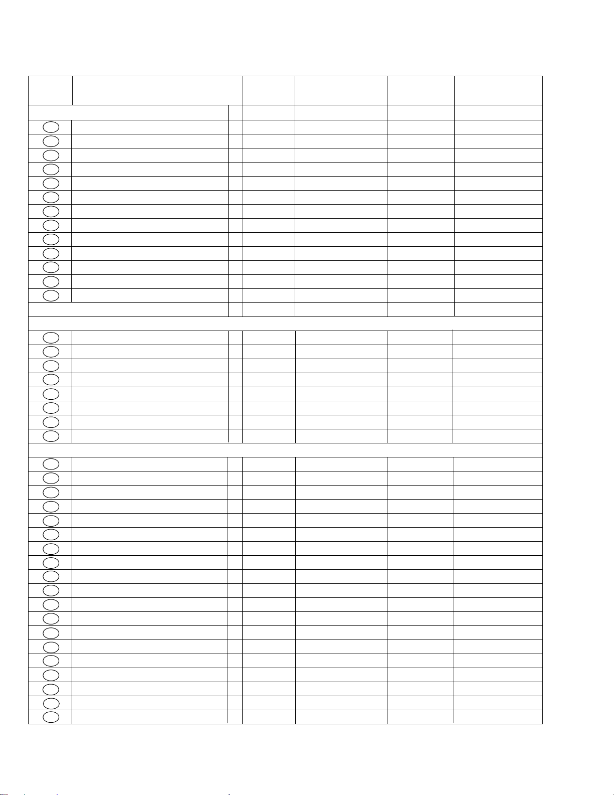
Step
Part Name Fig.
Point
Note
Remarks
A Cassette housing assembly T Fig. 2-2-12 3(S1),(L1a)-(L1d) 1a, 1b, 1c, 1d Adjustment
2a
2b
2c
3a
3b
3c
3d
3e
4a
4b
4c
5a
5b
B
Reel disk (SUP) assembly T Fig. 2-2-13 (W2) 2a, 2b
Reel disk (TU) assembly T Fig. 2-2-13 (W2) 2a, 2b
Reel cover assembly T Fig. 2-2-13 (S2b),2(S2a),(W2) 2c, 2d
Tension arm assembly T Fig. 2-2-14 (W3a) 3b
Release guide assembly T Fig. 2-2-14 - 3a
Idler arm assembly T Fig. 2-2-14 (W3b) Guide arm assembly T Fig. 2-2-14 - 3a
Pinch roller arm assembly T Fig. 2-2-14 (W3a) Cleaner arm assembly T Fig. 2-2-15 (L4a) 4a
Slant pole arm assembly T Fig. 2-2-15 (W4),(L4b),(P4a),(P4b) 4b
Drum assembly T Fig. 2-2-15 3(S4) - Adjustment
Guide roller (S) assembly T Fig. 2-2-16 (P5) 5a, 5b Adjustment
Rail assembly T Fig. 2-2-16 3(W5a), (W5b) 5c, 5d
Slide deck assembly /C Main deck assembly
T Fig. 2-2-17 (W6),(L6a)-(L6d) 6a, 6b (Adjustment)
B Slide deck assembly
7a
7b
7c
7d
7e
7f
7g
7h
Loading brake assembly T Fig. 2-2-18 (W7),(L7a),(P7a) 7e Adjustment
Guide pin (SUPPLY) T Fig. 2-2-18 (S7a) Pad arm assembly T Fig. 2-2-18 (W7),(L7b),(P7b) 7d
Slide guide plate assembly T Fig. 2-2-18 (S7b) 7c Adjustment
Collar T Fig. 2-2-18 - 7a
Collar T Fig. 2-2-18 - 7a
Sub brake assembly T Fig. 2-2-18 (W7),(L7c),(P7c) 7b
Control plate assembly T Fig. 2-2-18 2(W7),(L7d),(P7d) 7b
C Main deck assembly
8a
8b
8c
9a
9b
9c
9d
9e
9f
10a
10b
10c
10d
10e
11a
11b
11c
11d
11e
Tension lever assembly T Fig. 2-2-19 - 8c
Slide lever assembly T Fig. 2-2-19 - 8b
Brake control lever assembly T Fig. 2-2-19 - 8a
Loading guide T Fig. 2-2-20 (S9) Timing belt T Fig. 2-2-20 - 9b
Center gear assembly T Fig. 2-2-20 - Motor bracket assembly T Fig. 2-2-20 2(S9) 9a
Worm wheel T Fig. 2-2-20 (W9) - (Phase adjustment)
Gear holder T Fig. 2-2-20 (S9) Main cam gear T Fig. 2-2-21 (S10) 10b Phase adjustment
Brake control plate T Fig. 2-2-21 (L10) 10b Phase adjustment
Rotary encoder T Fig. 2-2-21 (S10),(W10a) 10a Phase adjustment
Connect gear T Fig. 2-2-21 (W10a) - (Phase adjustment)
Reel drive pulley assembly T Fig. 2-2-21 (W10b) Catcher (T) assembly T Fig. 2-2-22 2(S11) Capstan motor T Fig. 2-2-22 2(S11) Charge arm assembly T Fig. 2-2-22 (W11) 11
Sub cam gear T Fig. 2-2-22 (S11) - Phase adjustment
PWB holder B Fig. 2-2-22 2(S11) -
2-5
Table 2-2-2
Page 23
5b
9e
10c
8a
9f
10d
3a
7c
2a
BSlide deck
assembly
9d 5a 4c 4a 4b
11b 11a
7b 7a 7d 7e 9c 3c 3b 7h 2b
CMain deck
assembly
10e
3d
9a
2c
3e
9b
8c
7f
7g
11e
11d
11c
BSlide deck
assembly
Fig. 2-2-10 Top view
CMain deck
assembly
10a
10b
8b
Fig. 2-2-11 Bottom view
2-6
Page 24
2.2.5 Disassembly/assembly
1.
A Cassette housing assembly
(L1b)
1
(S1)
2
(S1)
(L1b)
(L1d)
(L1c)
Note 1c
Cassette
A
housing
assembly
(L1a)
Note 1b
Slide deck assembly
/Main deck assembly
3
(S1)
(L1a)
<STOP mode>
<EJECT mode>
<PLAY mode>
Note 1a:
Shift the mechanism mode
from the STOP mode to the
EJECT mode.
Note 1b:
Reassemble the cassette
housing assembly to the
mechanism as the cancel lever
is moved in the direction of the
arrow.
Note 1c:
When reassembling the cassette housing to the mechanism, make sure that there is
no deformation in the frame or
no damage to the switches,
etc.
Note 1d:
After reassembling the component parts, check the mechanism operation in the PLAY
mode.
For details of checking method,
refer to “2.2.8 assembling slide
deck assembly and main deck
assembly”.
Fig. 2-2-12
2a
2. Reel disk (SUP) assembly
2b
Reel disk (TU) assembly
2c
Reel cover assembly
(W2)
Note 2b
(W2)
2a
4
(S2a)
6
(S2b)
5
(S2a)
2c
Note 2a
Note 2c
Note 2a
Fig. 2-2-13
2b
Note 2b
(W2)
Note 2c
Slide deck assembly
/Main deck assembly
Note 2a:
When removing the reel disk assembly, be careful not to break
the brake pad which applies lateral pressure to the reel disk.
Note 2b:
Be careful not to make a mistake in installing the reel disk.
The SUP reel disk and TU reel disk can be distinguished from
each other by the appearance as shown below.
(SUP) (TU)
Note 2c:
When removing the reel cover assembly, pay heed to the guide
arm assembly. For, the guide arm assembly is just inserted
into the slide deck assembly from the upside and it is apt to
come off after the reel cover assembly is removed.
Note 2d:
When fitting the reel cover assembly to the set, carefully tighten
the screw with the specified tightening torque of 0.069N·m
(0.7kgf·cm).
2-7
Page 25
3. Tension arm assembly/ Release guide assembly
3c
Idler arm assembly/ Guide arm assembly
3e
Pinch roller arm assembly
3b3a
3d
(W3a)
3d
3a
Note 3a
3b
3c
Note 3a
(W3b)
(W3a)
3e
Note 3b
Note 3a:
When removing the reel cover assembly, pay heed to release
guide assembly and guide arm assembly. For, the guide arm
assembly is just inserted into the slide deck assembly from
the upside and it is apt to come off after the reel cover assembly is removed.
Note 3b:
Reassemble the tension arm assembly to the mechanism as
the pad arm assembly is moved to the extent in the direction
of the arrow.
Fig. 2-2-14
4a
4. Cleaner arm assembly/
4c
Drum assembly
7
(S4)
9
(S4)
4c
4b
Slant pole arm assembly
8
(S4)
4a
(L4a)
Note 4a
Note 4b
(P4b)
(P4a)
(W4)
4b
(L4b)
Note 4a:
When removing the cleaner arm assembly, it is recommended
to remove the slant pole arm assembly together with it except
the case of a single unit replacement, because the hook (L4a)
is hard to disengage.
Note 4b:
How to set the coil spring (P4b).
(P4b)
4a
4b
(P4b)
Fig. 2-2-15
2-8
Page 26

5a 5b
5. Guide roller (SUPPLY) assembly/
Rail assembly
(W5b)
5b
5a
Note 5a
(W5a)
(W5a)
(P5)
Note 5b
Note 5c
(W5a)
Note 5d
Note 5a:
When reassembling, insert the tip
of the guide roller with the coil
spring put on it into the hole on
the main deck. Tighten the guide
roller by about 6 turns so that the
height of the guide roller assembly is 19 mm or so as shown in
the figure.
Note 5b:
Pay careful attention to the spring not to lose it.
Note 5c:
Pay careful attention to the engagement of the rail assembly’s
arm ends because they easily come off the engagement.
Moreover, make sure that there is neither deformation nor
damage observed in them.
Note 5d:
When removing the rail assembly, check to see if the collar is
securely set in the arm groove.
Guide roller
(s) assembly
19mm
Fig. 2-2-16
B Slide deck assembly/ C Main deck assembly
6.
(L6a)
(W6)
BSlide deck assembly
(L6b)
Note 6a
(L6d)
CMain deck
assembly
(L6c)
Note 6b
Note 6a:
When removing the slide deck assembly, pay heed to the three
components of the following because they are apt to come off
after the slide deck assembly is removed.
8a
Tension lever assembly/ Slide lever assembly
Brake control lever assembly
8c
For reassembling those components, refer to Fig. 2-2-19 on
page 2-10.
Note 6b:
When reassembling the slide deck assembly to the main deck
assembly, combine them with each other by the side grooves
and then slide the slide deck assembly by 1 mm or so.
8b
1mm
2-9
Fig. 2-2-17
Page 27

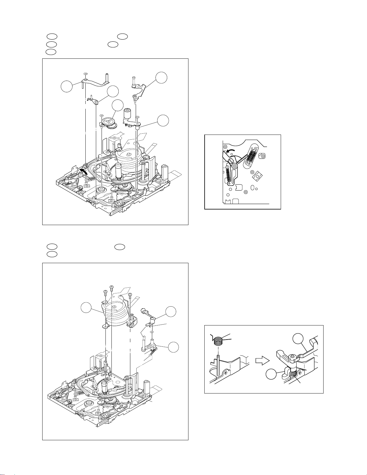
Note 7b
7a
7. Loading brake assembly/ Guide pin (S)
7c
Pad arm assembly/
7e
Collar/ Collar/ Sub brake assembly
7h
Control plate assembly
7f
Slide guide plate assembly
7g
(W7)
(P7b)
10
(S7a)
7b
7d
Note 7d
7c
11
(S7b)
7b
Note 7c
7d
(W7)
7g
Note 7a:
Don’t remove these parts unreasonably. If they are removed
for some reason, be very careful not to lose them.
Note 7b:
When reinstalling the sub brake assembly, set the control plate
assembly so that its hook is set in the
assembly.
‹
part of the sub brake
(P7a)
7a
Note 7e
(P7d)
(L7b)
(W7)
(W7)
7e
7f
Note
7a
(W7)
(P7c)
Note 7b
7h
(L7a)
(L7d)
Fig. 2-2-18
8. Tension lever assembly/ Slide lever assembly
8a
8c
Brake control lever assembly
Note 8c
8a
8b
(L7c)
8c
8b
Note 8a
Note
8b
Note 7c:
Since the slide guide plate assembly controls the slide deck
assembly so that it exactly slides the main deck assembly, it
must exactly be assembled in the PLAY mode. Therefore,
temporarily fix the slide guide plate assembly in this stage.
For details of reassembling procedure, refer to “2.2.8
Assembling slide deck assembly and main deck assembly” on page 2-15.
Note 7d:
The pad arm assembly controls the tension level of the tension arm assembly. For adjustment of the tension arm assembly, refer to page 2-8.
Note 7e:
When reinstalling the load brake assembly, slightly lift the
slide deck assembly upwards because the lower part of the
load brake assembly sticks out of the slide deck assembly.
Note 8a, 8b, 8c:
For refitting the respective parts, refer to the following figures
8a 8b
Tension lever assembly Slide lever assembly
Fig. 2-2-19
Brake control lever
8c
assembly
2-10
Page 28

9a
9. Loading guide/ Timing belt
9c
Center gear assembly/ Motor bracket assembly
9e
Worm wheel/ Gear holder
9b
9b
9f
Note 9b
9d
Note 9a
9d
9c
14
(S9)
13
(S9)
15
(S9)
(W9)
9e
9f
12
(S9)
Note 9a:
Carefully handle the DEW sensor. (Don’t touch the sensor surface in particular.)
Note 9b:
When engaging the timing belt, make sure that it securely engages with the gears of both the center gear assembly and
reel drive pulley assembly.
9a
10a
10. Main cam gear/
10c
Rotary encoder/
10e
Reel drive pulley assembly
(W10a)
16
(S10)
10a
10b
Note
10b
(L10)
Note 10a
Fig. 2-2-20
10b
Brake control plate
10d
Connect gear
17
(S10)
10c
(W10a)
10d
(W10b)
10e
Note 10a:
When removing/refitting parts, pay careful attention to the
flexible board and so on not to damage them.
Note 10b:
When reinstalling the main cam gear and the brake control plate,
first fit them together so that the protrusion on the brake control
plate is set in the slot on the main cam gear as shown below,
next install the two together to the main deck assembly.
10a
10b
2-11
Note 10b
Fig. 2-2-21
Page 29

11. Catcher (T) assembly/ Capstan motor
11a
Charge arm assembly/ Sub cam gear
11c
11e
PWB holder
11b
11d
18
(S11)
19
(S11)
(W11)
Note 11
21
(S11)
11c
20
(S11)
22
(S11)
11d
11b
11a
Note 11:
The following figure shows how to put the charge arm assembly and sub cam gear assembly together.
11d
11c
11e
24
(S11)
Fig. 2-2-22
23
(S11)
2-12
Page 30

2.2.6 List of procedures for disassembly
Cassette housing assembly
A
(L1b)
1
(S1)
(W3b)
3c
(W10b)
5b
(W5a)
(W5a)
5a
(P5)
(W5b)
(W5a)
14
(S9)
13
(S9)
9d
(L1d)
(W6)
7d
11
(S7b)
4
(S2a)
2
(S1)
(P7a)
7b
7a
2a
8b
AA
10b
(S7a)
(W2)
(L1c)
10a
10
(W7)
6
(S2b)
(S10)
(P7b)
7c
(P7d)
5
(S2a)
16
(W7)
AA
(S9)
(W3a)
(W7)
15
7h
AA
(W7)
(W2)
8
9
(S4)
(P4b)
12
22
(S11)
9a
(W11)
7
(S4)
4a
(P4a)
3e
(S4)
4c
(W4)
4b
(W3a)
11c
AA
(L1a)
3
(S1)
(W10a)
10c
8a
9f
3a
BB
2b
(S10)
AA
(W9)
AA
BB
7e
7f
BSlide deck
assembly
9c
7
9e
3b
(W10a)
10d
AA
BB
9b
10e
(S11)
20
(S11)
21
(S11)
CMain deck
assembly
3d
(W7)
7g
(P7c)
19
BB
18
(S11)
11a
11b
(S9)
AA
8c
AA
11d
(W2)
2c
Note 3b
Note)
Classification Part No. Symbol in drawing
Grease KYODO-SH-P AA
Oil YTU94027 BB
2-13
Fig. 2-2-23
24
(S11)
11e
23
(S11)
Page 31

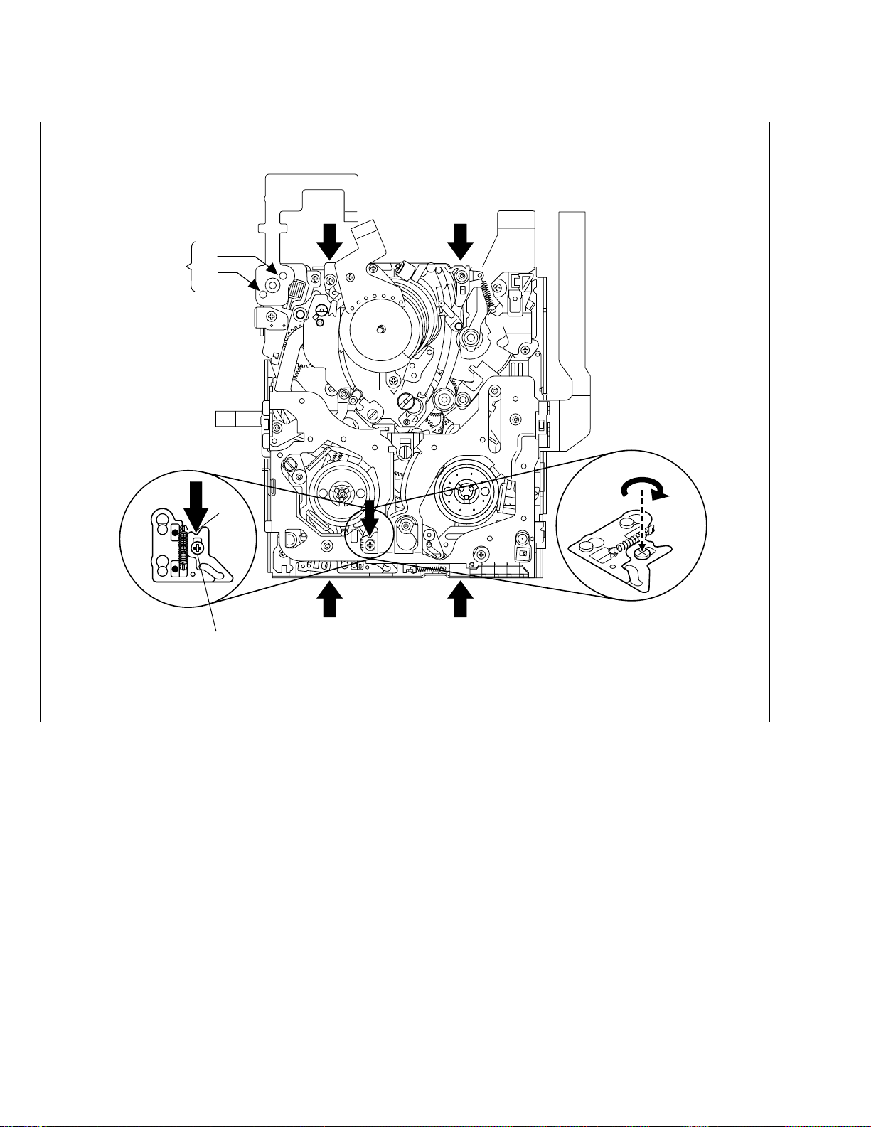
2.2.7 Checkup and adjustment of mechanism phase
<Rotary encoder>
Set the “■” of the rotary
part at the tapped hole
as shown in the figure.
<Worm wheel> (Note 2)
Set the worm wheel so
that its locating hole
meets the hole on the
main deck assembly.
<Main cam gear
/Brake control plate>
After fitting the main cam\
gear and brake control plat
together,set them together
so that their locating holes
meet the hole on the main \
deck assembly.
<Connect gear> (Note 2)
Set the connect gear so
that its locating hole meets
the hole on the main deck
assembly.
Note 1
<Connect gear 2> (Note 2)
Set the connect gear 2 so
that its locating hole meets
the hole on the main deck
assembly.
<Sub cam gear>
Set the sub cam gear
so that its locating hole
meets the hole on the
main deck assembly.
This state represents
that the mechanism is
in the EJECT mode,
which is the “mechanism
assembly mode”.
Note 1:
Since the connect gear 2 is tightly fixed to the main deck
by caulking, adjust its phase with the connect gear and
sub cam gear.
Fig. 2-2-24
Note 2:
The part that needs phase adjustment by the hole on the main
deck assembly must exactly be set as the specified phase.
There is a fear that some part is installed in a wrong phase
because assembling of the mechanism is automated. If so,
set every part in the correct phase whenever the mechanism
is reassembled.
2-14
Page 32
2.2.8 Assembling slide deck assembly and main deck assembly
CC
2
3
œ
Œ
D
A
3
3
3
3
BB
1
Assembling procedure
1. Loosen the screw A.
2. Set the mechanism in the PLAY mode.
(Refer to page 2-2.)
3. Press the end face B of the slide deck assembly (reel
disk side) and the end face C of the main deck assembly (drum assembly side) with uniform force so that the
two assemblies are tightly pressed to each other. Furthermore, press the part D and tighten the screw A.
Note :
Tightening torque for screw A: 0.069 N·m (0.7 kgf·cm)
2-15
Fig. 2-2-25
Page 33
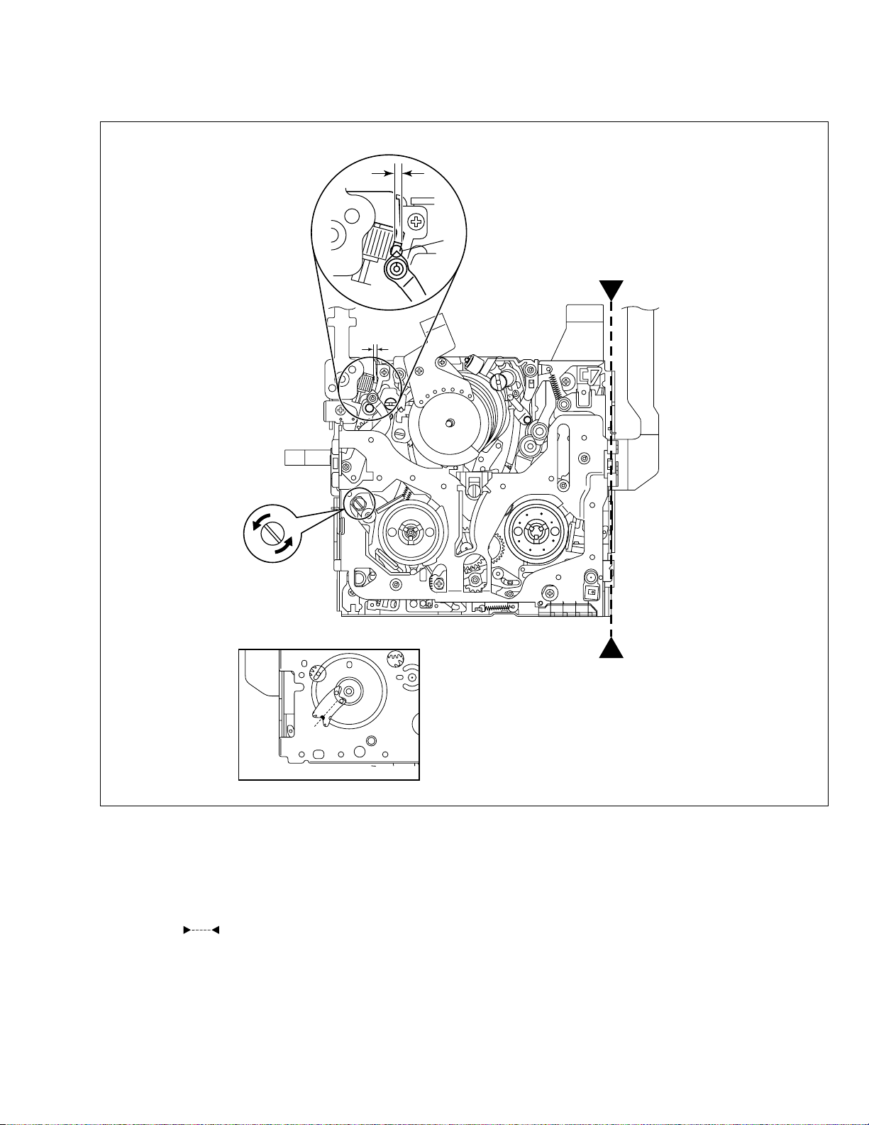
2.2.9 Locating tension pole
b
a
c
<PLAY mode>
Locating procedure
1. Enter the mechanism assembly into the PLAY mode.
(Refer to page 2-2.)
2. When the “
the part “a” of the tension arm assembly is located within
the range of “b”.
3. If the part “a” is out of the range, turn the pin “c” to
adjust the position.
” part is positioned down, make sure that
Fig. 2-2-26
2-16
Page 34
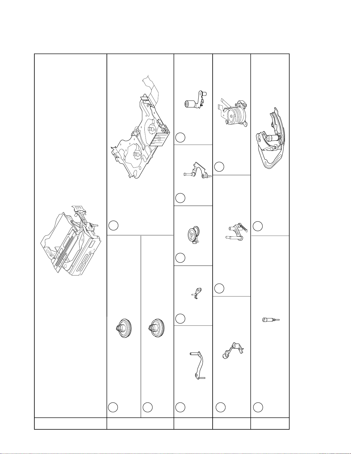
2.3 SERVICE NOTE
1
2
3
4
5
A Cassette housing assembly
S1×3
W2×1
Reel disk (SUP) assembly
W2×1
W3a×1
P5×1
Reel cover assembly
S2a×2
S2b×1
W2×1
Reel disk (TU) assembly
Tension arm assembly
Release guide
assembly
W3b×1
Idler arm assembly
W3a×1
Pinch roller arm assembly
Guide arm assembly
Cleaner arm assembly
W4×1 P4a×1 P4b×1
Slant pole arm assembly
S4×3
Drum assembly
Guide roller (S) assembly
W5a×3 W5b×1
Rail assembly
2a
2b
3a
3b
3c
3d
3e
2c
4b
5b
4a
5a
4c
Use the following chart to manage mechanism parts that are removed for disassembling the mechanism.
Table 2-3-1a
2-17
Page 35
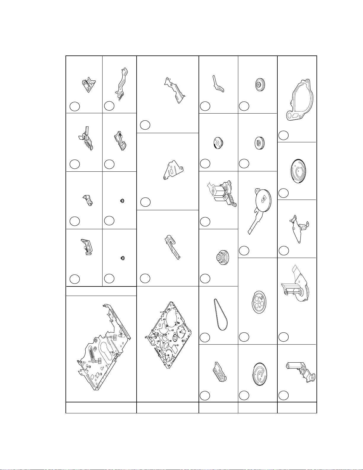
6
8
7
9
10
11
W7×1 P7a×1
S9×1
S10×1
S11×2
Loading brake
assembly
Collar
S7a×1
Guide pin (SUPPLY)
Collar
W7×1 P7b×1
Pad arm assembly
W7×1 P7c×1
Sub brake assembly
S7b×1
Slide guide plate
assembly
Control plate
assembly
W7×2 P7d×1
W7×1
B Slide deck assembly
C Main deck assembly
Tension lever assembly
Slide lever assembly
Brake control lever assembly
Loading guide Timing belt
Center gear
assembly
S9×2
Motor bracket
assembly
W9×1
Worm wheel
S9×1
Gear holder
Main cam gear Brake control plate
S10×1 W10a×1
W6×1
Rotary encoder
W10a×1
Connect gear
W10b×1
Reel drive pulley
assembly
Catcher (T) assembly
S11×2
Capstan motor
W11×1
Charge arm assembly
S11×1
Sub cam gear
S11×2
PWB holder
7a
7b
7e
8b
9c
9d
9e
9f
10d
10c
11c
11d
11e
10b
10a
11b
11a
10e
8a
9b
9a
7f
7c
7g
8c
7d
7h
Table 2-3-1b
2-18
Page 36
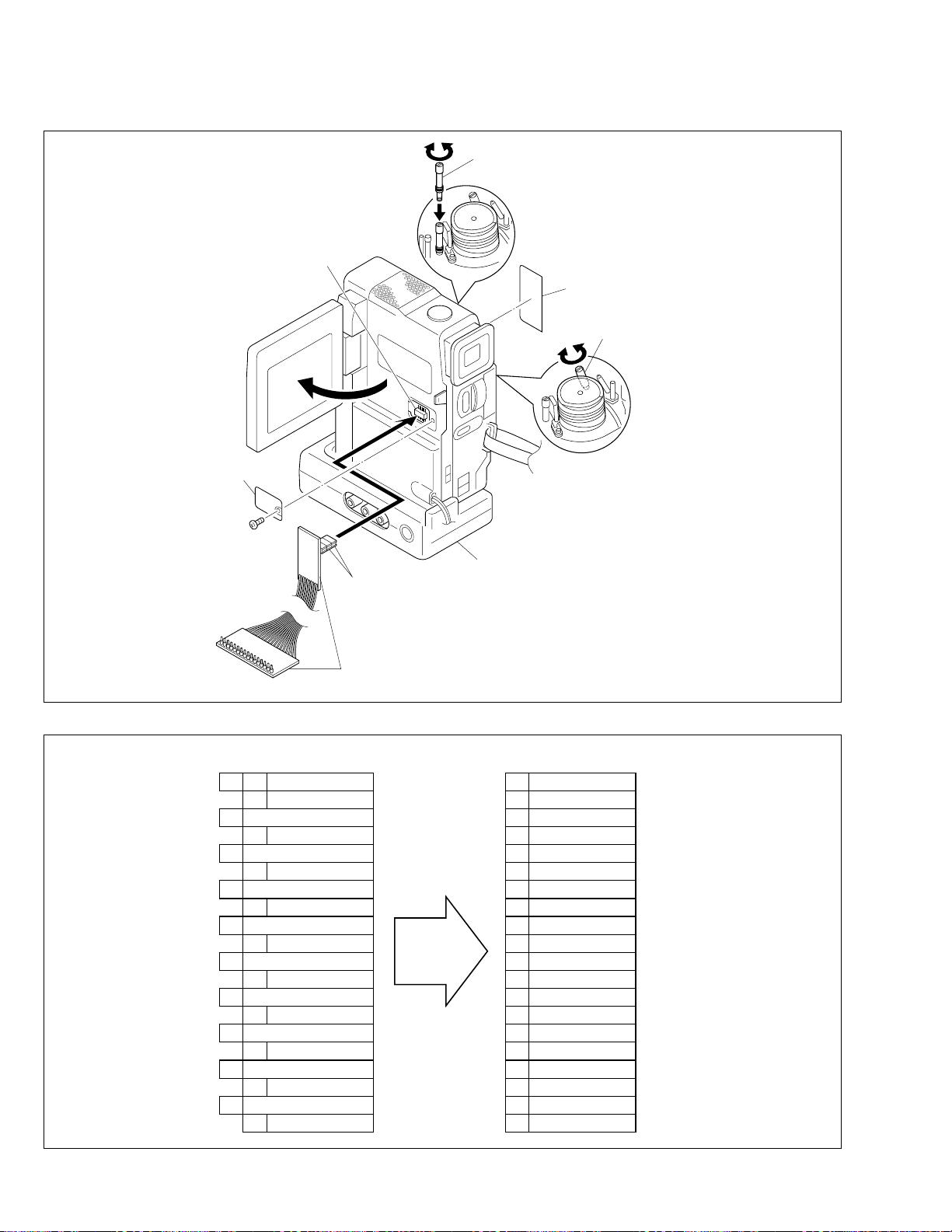
2.4 JIG CONNECTOR CABLE CONNECTOR
Remove one screw (1) first and the cover (JIG) next.
CN1010
COVER
(JIG)
1
GUIDE ROLLER (SUP) ASSY
SHEET
GUIDE ROLLER
(TU) ASSY
DOCKING STATION
EXTENSION
CONNECTOR
For supplying the power through the coupler by
NOTE)
removing the cover (for jig), use this extension
connector double for connecting the jig connector
cable.
JIG CONNECTOR
CABLE
Fig. 2-3-1 Jig connector cable connection
MAIN BOARD ASSEMBLY JIG CONNECTOR CABLE
D_REG2.91
JIG_SPT11
JIG_SCK2
JIG_MOD12
RST3
VPP13
SBD4
SBT14
AL_3VSYS5
PB_VCO15
MAIN_VCO6
ENV_OUT16
ATFI7
FS_PLL17
HID8
SBE18
UNREG9
GND19
UNREG10
GND20
D_REG2.91
JIG_SCK2
RST3
SBD4
AL_3VSYS5
MAIN_VCO6
ATFI7
HID8
UNREG9
UNREG10
JIG_SPT11
JIG_MOD12
VPP13
SBT14
PB_VCO15
ENV_OUT16
FS_PLL17
SBE18
GND19
(GND)20
2-19
Fig. 2-3-2 Jig connector cable schematic diagram
Page 37
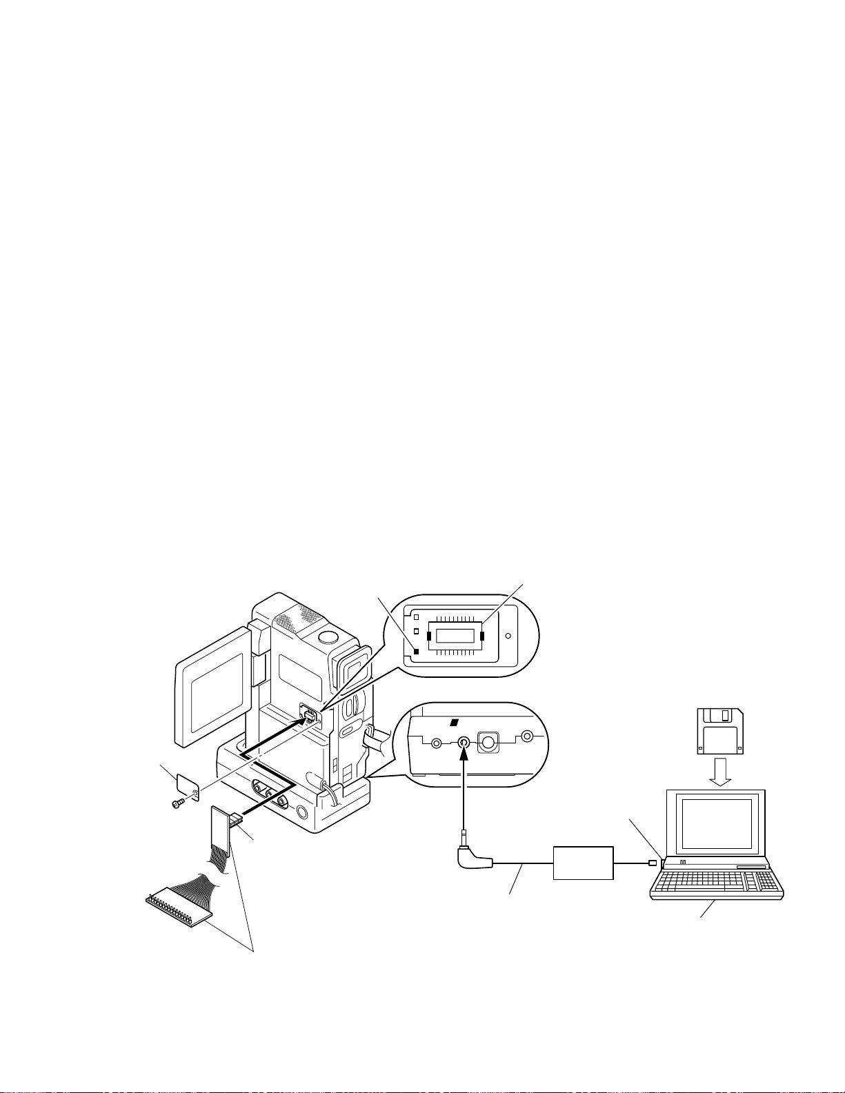
SECTION 3
Service Support
System software
RS232C
COM Port
PC CABLE
EXTENSION CONNECTOR
Personal Computer
MENU
JLIP
/ EDIT
J
10 1
20
CN1010
(JIG CONN.)
TL3501
REC MON
11
JIG CONNECTOR
CABLE
1
COVER
(JIG)
Note) For supplying the power
through the coupler by
removing the cover (for jig),
use this extension connector
double for connecting the
jig connector cable.
ELECTRICAL ADJUSTMENT
3.1 PREPARATION
1. Precaution
Both the camera and deck sections of this model needs a
personal computer for adjustment except simple adjustment with potentiometers. If some of the following parts is
replaced for repair or other reason, the repaired set must
be adjusted with a personal computer.
• OP block
2
• E
PROM (IC1003 of MAIN board)
• MONITOR
2
• E
P ROM (IC7603 of MONITOR board)
In the event of malfunction with electrical circuits, troubleshooting with the aid of proper test instruments most be
done first, and then commence necessary repair, replacement and adjustment, etc.
1. In case of wiring to chip test points for measurement, use
IC clips, etc. to avoid any stress.
2. Since connectors are fragile, carefully handle them in
disconnecting and connecting.
3. Shortcircuit between operation un it and DECK chassis.
3.2 SETUP
1. Setup for electrical adjustment with personal computer
2. Required test equipment
1. Color TV monitor.
2. AC power adapter/charger
3. Oscilloscope (dual-trace type, observable 100 MHz or
higher frequency)
Note:
It is recommended to use one observable 300 MHz or
higher frequency.
4. Digital voltmeter
5. Frequency counter (with threshold level adjuster)
6. Personal computer
3. Required adjustment tools
For detsails of special jigs necessary for adjustment, refer to
page 1-2 and 1-3 of the Section 1.
Fig. 3-2-1 Connection for Service support system
3-1
Page 38
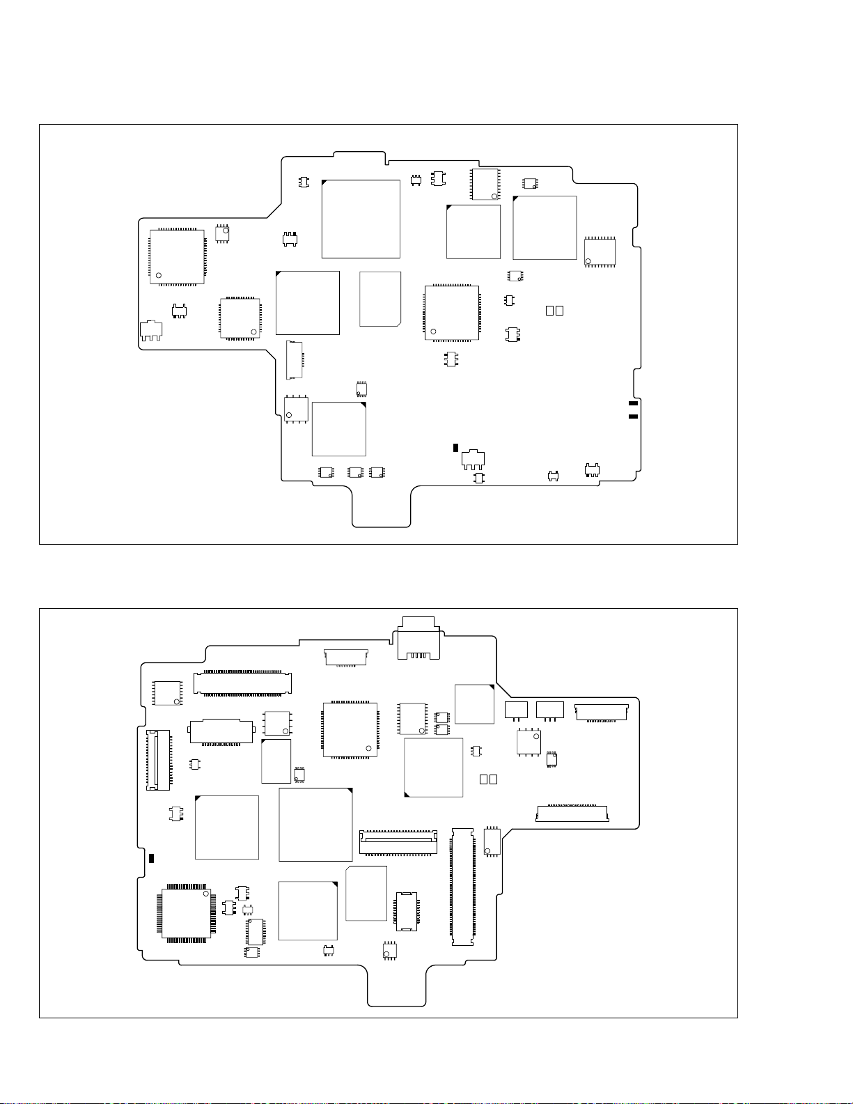
3.3 FUSE LOCATION
3.3.1 MAIN PWB (FOIL SIDE)
49
64 17
1
3348
IC5001
116
4
3
15
IC5002
IC4202
3
32
IC1101
36
14
85
24
IC4201
372548 13
IC4302
112
IC3004
34
113
4
IC4301
CN1005
IC1003
IC3203
11
33
161
20
IC1002
IC3201
32
17
10
IC1402
1
85
5
314
IC3202
IC6401
43
5
58
14
IC1401
41
IC1403
0 1 MAIN PWB
1
20
11
IC3701
110
F6103
F6101
3
1
5
4
IC3005
5
314
5
IC3001
5
48
49
IC3002
16
IC1006
58
41
85
41
64
IC3301
1
6
34
IC3851
IC1001
58
IC1009
41
85
IC1005
85
14
14
IC1008
F6104
1
213
3
4
IC6003
IC6004
2
IC6001
3
4
5
1
3
1
IC6002
4
3.3.2 MAIN PWB (COMPONENT SIDE)
40
81
916
322
21
40
IC2751
CN1014
331
IC3702
5
F6102
20
IC6101
41 60
IC2701
3
314
CN1002
80
CN1008
16 1
541
IC8003
1
80
43
51
IC8007
61
IC8006
4
5
110
IC8008
14
3
IC8005
1
5
4
1
3
IC8102
Fig. 3-3-1 Fuse location for MAIN board assembly
J101
14
IC8009
85
14
33 48
IC8001
IC8101
CN1001
81
32 49
IC8103
43
51
IC3501
17
64
45
IC8002
16 1
CN1007
20 11
85
14
IC1405
11 20
IC4401
CN1010
IC4304
14
41
IC3801
8
5
IC4305
8
5
IC3101
IC4303
135
CN1009
21
41
IC5004
4
10
1
0 1 MAIN PWB
IC1004
244
1
110
85
50
14
CN1016
51100
1
1
41
58
IC1201
IC8004
1120
85
CN1004
IC6601
41
85
5
120
CN1011
13
12 1
8
CN1003
3-2
Fig. 3-3-2 Fuse location for MAIN board assembly
Page 39

3.3.3 MONITOR PWB (COMPONENT SIDE)
33 48
16 1
17
32
64
49
1
CN7502
IC7601
IC7502
F7501
24
18
916
16 9
18
1
2
3
15
4
39
38
14
5
IC7603
IC7501
IC7604
CN7501
8
5
4
1
3
IC7607
IC7608
4
51
3
0 4 MONITOR PWB
Fig. 3-3-3 Fuse location for MONITOR board assembly
3-3
Page 40
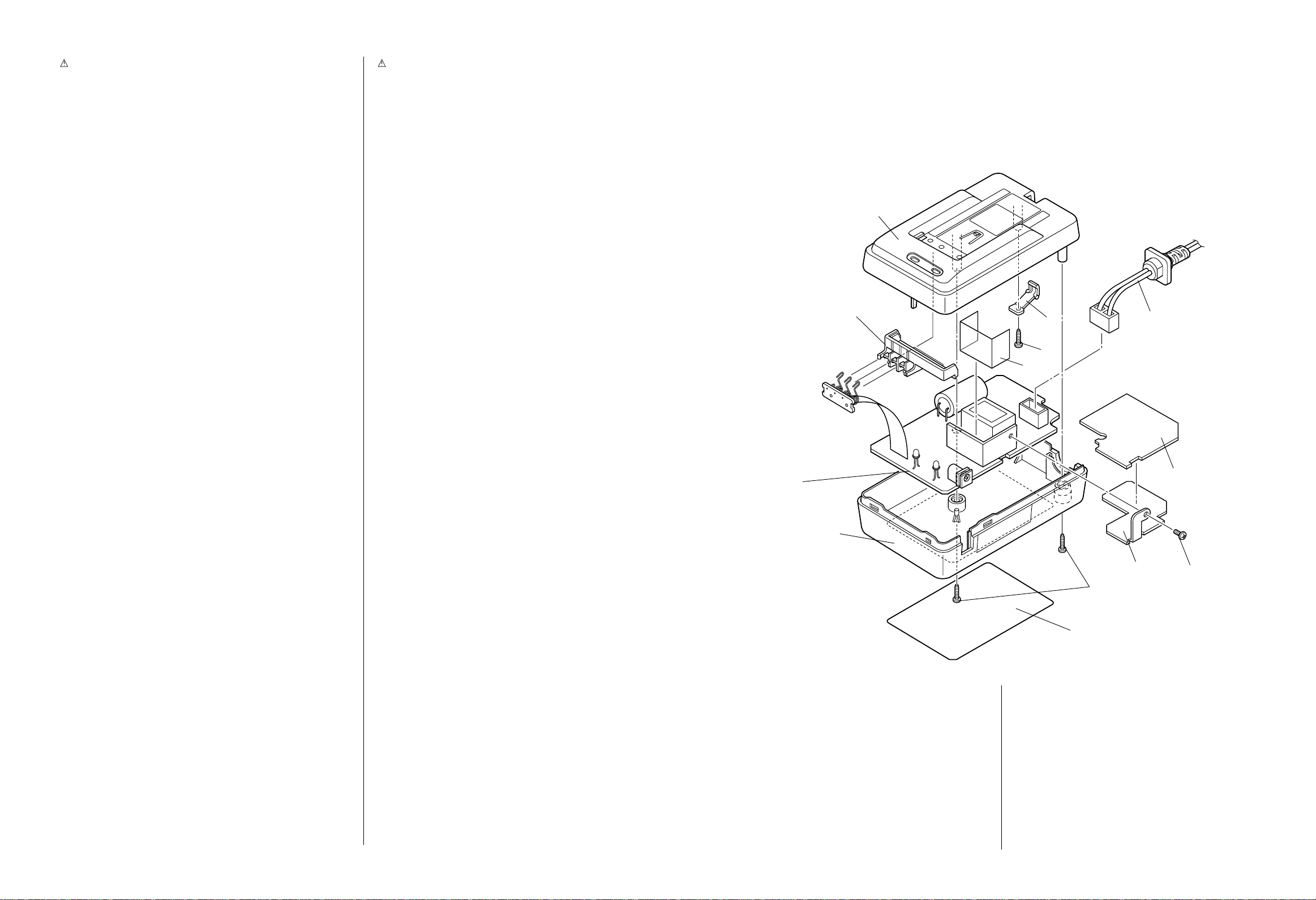
SECTION 6
# REF No. PART No. PART NAME, DESCRIPTION # REF No. PART No. PART NAME, DESCRIPTION
---------------- ----------------------- ----------------------------------------------------- ----------------- ----------------------- -----------------------------------------------------
C2627 NCBA1HK-102W CAPACITOR 0.001µF,50V
C2628 NCBA1HK-102W CAPACITOR 0.001µF,50V
C2629 NBE20GM-336X T CAPACITOR 33µF,4.0V
C2631 NCB31EK-103X CAPACITOR 0.01µF,25V
C2632 NCB31EK-103X CAPACITOR 0.01µF,25V
C2635 NCB30JK-105X CAPACITOR 1µF,6.3V
C2636 NCB30JK-105X CAPACITOR 1µF,6.3V
C2639 NCB31CK-104X CAPACITOR 0.1µF,16V
C2640 NCB31CK-104X CAPACITOR 0.1µF,16V
C2702 NBE90GM-226X T CAPACITOR 22µF,4.0V
C2703 NBE90GM-226X T CAPACITOR 22µF,4.0V
C2753 NCB20JK-225X CAPACITOR 2.2µF,6.3V
C2754 NCB20JK-225X CAPACITOR 2.2µF,6.3V
C2764 NCB20JK-225X CAPACITOR 2.2µF,6.3V
C2765 NCB20JK-225X CAPACITOR 2.2µF,6.3V
C2766 NCB21CK-474X CAPACITOR,E,F 0.47µF,16V
C2767 NCB21CK-474X CAPACITOR,E,F 0.47µF,16V
C2768 NRSA63J-0R0X MG RESISTOR 0Ø,1/16W
C2769 NRSA63J-0R0X MG RESISTOR 0Ø,1/16W
C7427 NBP41DM-106X T CAPACITOR 10µF,20V
C7428 NCB21CK-105X CAPACITOR 1µF,16V
C7429 NBE21AM-106X T CAPACITOR 10µF,10V
C7431 NBE20JM-106X T CAPACITOR 10µF,6.3V
L2101 NQL402M-100X COIL 10µH
L2102 NQL402M-100X COIL,C,D,E,F 10µH
L2131 NQL402M-100X COIL 10µH
L2601 NRSA63J-0R0X MG RESISTOR 0Ø,1/16W
L2602 NRSA63J-0R0X MG RESISTOR 0Ø,1/16W
L2603 NRSA63J-0R0X MG RESISTOR 0Ø,1/16W
L2604 NRSA63J-0R0X MG RESISTOR 0Ø,1/16W
L7403 NQL045K-100X COIL 10µH
L7404 NQL045K-100X COIL 10µH
S7001 NSW0129-001X PUSH SWITCH
CN801 QGB0401L1-A0X CONNECTOR
CN802 QGF0517F2-12X FPC CONNECTOR
CN803 QGF0517F1-06X FPC CONNECTOR
CN804 QGA1001F1-05X CONNECTOR
CN805 QGF0507F1-20X FPC CONNECTOR
OT1 LY42535-001A SHEET(AUD.PWB)
OT2 LY42775-001A S.SHEET(AU/VF)
L2852 NQR0251-004X FERRITE BEAD
L2853 NQR0251-004X FERRITE BEAD
J2851 QNS0078-001 3.5 JACK
CN901 QGF0507F1-16X FPC CONNECTOR
CN902 QGF0517F2-08X FPC CONNECTOR
✽✽✽✽✽✽✽✽✽✽✽✽✽✽✽✽✽✽✽✽✽✽✽✽✽✽✽✽✽✽
W/B BOARD ASSEMBLY <11>
PW3 YB10285A3 W/B BOARD ASSY
Q1151 RPM-22PB PHOTO TRANSISTOR
R1151 NRSA63J-302X MG RESISTOR 3kØ,1/16W
C1151 NBE90JM-106X T CAPACITOR 10µF,6.3V
C1152 NCB21EK-683X-R CAPACITOR 0.068µF,25V
L1151 NQR0265-001X FERRITE BEAD
WR1 WJM0144-001A E-SI C WIRE C-F
✽✽✽✽✽✽✽✽✽✽✽✽✽✽✽✽✽✽✽✽✽✽✽✽✽✽✽✽✽✽
EJECT BOARD ASSEMBLY
PW2 YB10288A2-01 EJECT BOARD ASSY
S1 NSW0120-002X PUSH SWITCH
WR1 WJM0145-001A E-SI C WIRE C-F
<12>
AC POWER ADAPTER (AA-V51EG/EK)
SAFETY PRECAUTION
Parts identified by the ! symbol are critical for safety. Replace only with specified part numbers.
6.1 CABINET ASSEMBLY <MA>
1
11
9
10
5
MAIN&
TERMINAL<91>
2
4
3
6
7
8
✽✽✽✽✽✽✽✽✽✽✽✽✽✽✽✽✽✽✽✽✽✽✽✽✽✽✽✽✽✽
JACK BOARD ASSEMBLY <09>
PW1 YB10288C1 JACK BOARD ASSY
Q2851 2SD1979/S/-X TRANSISTOR
D2852 MA8068 ZENER DIODE
R2851 NRSA63J-183X MG RESISTOR 18kØ,1/16W
R2852 NRSA63J-0R0X MG RESISTOR 0Ø,1/16W
R2853 NRSA63J-0R0X MG RESISTOR 0Ø,1/16W
R2854 NRSA63J-0R0X MG RESISTOR 0Ø,1/16W
R2855 NRSA63J-0R0X MG RESISTOR 0Ø,1/16W
C2854 NCB31EK-223X CAPACITOR 0.022µF,25V
C2856 NCB31EK-153X CAPACITOR 0.015µF,25V
C2859 NCB31HK-332X CAPACITOR 0.0033µF,50V
C2860 NCB31HK-102X CAPACITOR 0.001µF,50V
L2851 NQR0251-004X FERRITE BEAD
5-27
#!REF No. PART No. PART NAME, DESCRIPTION
----------------------- ------------------------------ ----------------------------------------------------------------------------
✽✽✽✽✽✽✽✽✽✽✽✽✽✽✽✽✽✽✽✽✽✽✽✽✽✽✽✽✽✽✽✽✽✽
CABINET ASSEMBL Y <MA>
! 1 PTY20603-013 UPPER CASE ASSY
! 2 PTY20483-023 LOWER CASE
! 3 YQ10531-006 POWER CORD For EG
PTY20080-034 POWER CORD For EK
4 YQ10531-011 SCREW,x2
! 5 PTY20483-078 INSULATOR B
! 6 PTY20483-076 SHILED PLATE
! 7 PTY20483-077 INSULA TOR A
6-1
RATING LABEL
#!REF No. PART No. PART NAME, DESCRIPTION
----------------------- ------------------------------ ----------------------------------------------------------------------------
8 PTY20483-079 SCREW, for shield plate
9 PTY20603-055 LOCK LEVER
10 PTY20545-055 SCREW
11 PTY20603-054 TERMINAL HOLDER
Page 41

6.2 SCHEMATIC DIAGRAM
Safety precautions
NOTE:
When ordering parts, be sure to order according to
the Part Number indicated in the Parts List.
The components identified by the symbol
cal for safety. For continued safety, replace safety
critical components only with manufacturer’s recom-
! are criti-
mended parts.
5
MAIN & TERMINAL
4
AC110
CN1
2200P
2200P
1221304
0.22
C35
0.22
TP16
TP15
CN2
SV
SV
3
PC123YS
R57
10
TERMINAL
2
OPEN
OPEN OPEN
OPEN
C36
0.22
PC123YS
8.45k
Q27
OPEN
OPEN
OPEN OPEN
OPEN
OPEN
R60
OPEN
1
ABCD E F G
6-2 6-3
Page 42

6.3 CIRCUIT BOARD
250V
T1.0A
6-4
Page 43

6.4 ELECTRICAL PARTS LIST
#!REF No. PART No. PART NAME, DESCRIPTION
----------------------- ------------------------------ ----------------------------------------------------------------------------
✽✽✽✽✽✽✽✽✽✽✽✽✽✽✽✽✽✽✽✽✽✽✽✽✽✽✽✽✽✽✽✽✽✽
MAIN & TERMINAL BOARD ASSY <91>
! PW1 PTY20603-503 MAIN & TERMINAL BOARD ASSY
! HS1 PTY20483-071 HEAT SINK A
! HS2 PTY20591-072 HEAT SINK B
OT1 PTY10067-551 SCREW
IC21 M61030AFP CHARGE COTROL IC 24pin SOP
Q1 FS2KM18A MOS FET
Q2 2SD2227 TRANSISTER
Q3 2SD2227 TRANSISTER
Q21 UN2211TX DIG.TRANSISTER
Q22 2SA1037AK/QR/-X CHIP TRANSISTER
Q23 2SB1592 TRANSISTER
Q24 2SA1037AK/QR/-X TRANSISTER
D1 S1WBA60 B.DIODE! 600V 1A
D5 1SS244T77 DIODE 200V 6A
D6 1SS244T77 DIODE 200V 6A
D21 MA7D56 DIODE 60V 10A
ZD1 MTZJ12C-T2 ZENER DIODE 12V
ZD2 MTZJ6.2B-T2 ZENER DIODE 6.2V 500mW
ZD21 MTZJ12C-T2 ZENER DIODE 12V
ZD22 MTZJ12C-T2 ZENER DIODE 12V
ZD23 MTZJ12C-T2 ZENER DIODE 12V
ZD24 MTZJ12C-T2 ZENER DIODE 12V
ZD25 MA4047NM ZENER DIODE 4.7V 500mW
LED1 YQ10531-540 LED RED POWER
LED2 YQ10531-542 LED GREEN CHARGE
R1 QRN141J-105 RESISTOR 1MΩ 1/4W
R3 PTY10067-601 MF RESISTOR 0.62Ω 1W
R4 QRE141J-334Y RESISTOR 330kΩ 1/4W
R5 QRE141J-334Y RESISTOR 330kΩ 1/4W
R7 QRE141J-751Y RESISTOR 750Ω 1/4W
R8 NRSA02J-103X MG RESISTOR 10kΩ 1/10W
R9 NRSA02J-272X MG RESISTOR 2.7kΩ 1/10W
R10 NRSA02J-104X MG RESISTOR 100kΩ 1/10W
R11 NRSA02J-682X MG RESISTOR 6.8kΩ 1/10W
R12 QRE141J-181Y RESISTOR 180Ω 1/4W
R13 QRE141J-334Y RESISTOR 330kΩ 1/4W
R14 QRE141J-334Y RESISTOR 330kΩ 1/4W
R15 NRSA02J-182X MG RESISTOR 1.8kΩ 1/10W
R16 NRSA02J-753X MG RESISTOR 75kΩ 1/10W
R22 NRSA02J-621X MG RESISTOR 620Ω 1/10W
R23 PTY20539-605 MF RESISTOR 0.20Ω 2W
R24 NRSA02J-102X MG RESISTOR 1kΩ 1/10W
R25 NRSA02J-101X MG RESISTOR 100Ω 1/10W
R26 NRSA02J-103X MG RESISTOR 10kΩ 1/10W
R27 NRSA02J-102X MG RESISTOR 1kΩ 1/10W
R28 NRSA02J-151X MG RESISTOR 150Ω 1/10W
R29 PTY20539-601 MG RESISTOR 47.0kΩ 1/10W
R30 PTY20539-601 MG RESISTOR 47.0kΩ 1/10W
R31 PTY20292-227 MG RESISTOR 10.0kΩ 1/10W
R32 NRSA02J-103X MG RESISTOR 10kΩ 1/10W
R33 NRSA02J-333X MG RESISTOR 33kΩ 1/10W
R34 PTY20539-601 MG RESISTOR 47.0kΩ 1/10W
R35 NRSA02F-8451X MG RESISTOR 8.45kΩ 1/10W
R36 NRSA02F-6192X MG RESISTOR 61.9kΩ 1/10W
R37 PTY20539-603 MG RESISTOR 1.0kΩ 1/10W
R38 PTY20539-601 MG RESISTOR 47.0kΩ 1/10W
R39 PTY20539-604 MG RESISTOR 1.3kΩ 1/10W
R40 PTY20450-200 MG RESISTOR 20.0kΩ 1/4W
R41 NRSA02F-1152X MG RESISTOR 11.5kΩ 1/10W
R42 NRSA02F-1152X MG RESISTOR 11.5kΩ 1/10W
#!REF No. PART No. PART NAME, DESCRIPTION
----------------------- ------------------------------ ----------------------------------------------------------------------------
R43 QRE141J-103Y MF RESISTOR 10kΩ 1/4W
R45 NRSA02J-222X MG RESISTOR 2.2kΩ 1/10W
R46 NRSA02J-472X MG RESISTOR 4.7kΩ 1/10W
R47 NRSA02J-221X MG RESISTOR 220Ω 1/10W
R48 NRSA02J-102X MG RESISTOR 1kΩ 1/10W
R49 NRSA02J-473X MG RESISTOR 47kΩ 1/10W
R57 NRSA02J-100X MG RESISTOR 10Ω 1/10W
! C1 QFZ9072-104 CAPACITOR 0.1µF 275V
C2 YQ10626-402 E CAPACITOR 47µF 400V
C3 PTY10067-651 CAPACITOR 1500pF 250V
C4 NCB21CK-224X CAPACITOR 0.22µF 16V
C5 PTY10067-653 CAPACITOR 0.01µF 50V
C6 NCB31HK-391X CAPACITOR 390pF 50V
! C7 PTY20538-611 CAPACITOR 2200pF 250V
! C8 PTY20538-611 CAPACITOR 2200pF 250V
C9 NDC31HJ-680X CAPACITOR 68pF 50V
C10 NDC31HJ-151X CAPACITOR 150pF 50V
C11 NDC31HJ-151X CAPACITOR 150pF 50V
C21 PTY10067-657 CAPACITOR 0.01µF 250V
C22 PTY20292-321 E CAPACITOR 680µF 16V
C23 QETL1CM-227 E CAPACITOR 220µF 16V
C24 PTY20603-601 CAPACITOR 0.22µF 10V
C25 NCF31EZ-104X CAPACITOR 0.1µF 25V
C26 PTY20603-601 CAPACITOR 0.22µF 10V
C27 NCB31CK-473X CAPACITOR 0.047µF 16V
C28 NCB31CK-473X CAPACITOR 0.047µF 16V
C29 NCB31CK-104X CAPACITOR 0.1µF 16V
C30 NCF31EZ-104X CAPACITOR 0.1µF 25V
C31 NCB31HK-222X CAPACITOR 0.0022µF 50V
C32 QEHA1HM-475 E CAPACITOR 4.7µF 50V
C33 NCF31EZ-104X CAPACITOR 0.1µF 25V
C34 NCF31EZ-104X CAPACITOR 0.1µF 25V
C35 QFLA1HJ-224 F CAPACITOR 0.22µF 50V
C36 NCB21CK-224X CAPACITOR 0.22µF 16V
! T1 PTY20538-801 SW TRANS
VR1 PTY20483-101 VOLUME 2kΩ
! F1 PTY20450-041 FUSE 1A 250V
JK1 YQ21032-301 DC JACK
! L1 PTY20450-401 LINE FILTER
L12 PTY10067-702 BEAD INDUCTOR
L21 PTY10067-703 COIL
! PHC1 PC123YS PHOTO COUPLER
TB1 PTY20603-053 TERMINAL, x3
WR1 PTY20603-052 FLAT CABLE, (4P)
CN1 PTY20603-056 CONNECTOR
6-5
 Loading...