

Page 1
SERVICE MANUAL
DIGITAL VIDEO CAMERA
VICTOR COMPANY OF JAPAN, LIMITED
VIDEO DIVISION
S40894
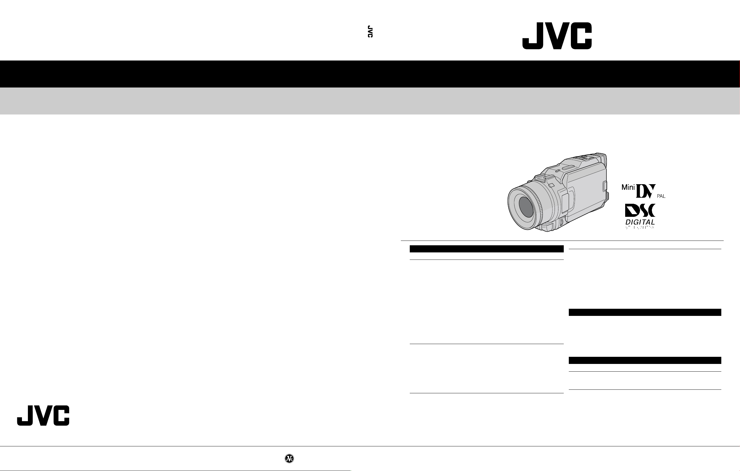
GR-DV1800EG/EK,DV2000EG/EK
GR-DV1800EG/EK,DV2000EG/EK
SPECIFICATIONS
For General
No. 86604
Power supply : DC 6.3 } V (Using AC Power Adapter/Charger)
Power consumption
LCD monitor off, viewfinder on : Approx. 4.4 W
LCD monitor on, viewfinder off : Approx. 5.3 W
Dimensions (W x H x D) : 74 mm x 90 mm x 178 mm
Weight : Approx. 660 g (without cassette, memory card and battery)
Operating temperature : 0°C to 40°C
Operating humidity : 35% to 80%
Storage temperature : –20°C to 50°C
Pickup : 1/4" CCD (Progressive Scan)
Lens : F 1.8, f = 3.8 mm to 38 mm, 10:1 power zoom lens
Filter diameter : ø52 mm
LCD monitor : 3.5" diagonally measured, LCD panel/TFT active matrix system
Viewfinder : Electronic viewfinder with 0.44" colour LCD
Speaker : Monaural
For Digital Video Camera
Format : DV format (SD mode)
Signal format : PAL standard
Recording/Playback format : Video: Digital component recording
Cassette : Mini DV cassette
Tape speed : SP: 18.8 mm/s
Maximum recording time : SP: 80 min.
(using 80 min. cassette) LP: 120 min.
For Digital Still Camera
Storage media : SD Memory Card/MultiMediaCard
Compression system : JPEG (compatible)
File size : 3 modes (UXGA: 1600 x 1200 pixels/XGA: 1024 x 768 pixels/
Picture quality : 2 modes (FINE/STANDARD)
Approximate number of storable images
(with the provided MultiMediaCard [8 MB])
FINE : 50 (VGA), 24 (XGA), 10 (UXGA)
STANDARD : 150 (VGA), 72 (XGA), 30 (UXGA)
(with an optional MultiMediaCard [16 MB])
FINE : 100 (VGA), 48 (XGA), 20 (UXGA)
STANDARD : 300 (VGA), 144 (XGA), 60 (UXGA)
DC 7.2 } V (Using battery pack)
(with the LCD monitor closed and the viewfinder pushed back
in, without the lens hood)
Approx. 740 g (incl. cassette, memory card and battery)
: Audio: PCM digital recording, 32 kHz 4-channel (12-bit),
48 kHz 2-channel (16-bit)
LP: 12.5 mm/s
VGA: 640 x 480 pixels)
Camcorder
For Connectors
AV
Video output : 1 V (p-p), 75 Ω, analogue
Video input (GR-DV2000 only) : 0.5 V (p-p) – 2.0 V (p-p), 75 Ω, analogue
Audio output : 308 mV (rms), 1 kΩ, analogue, stereo
Audio input (GR-DV2000 only) : 308 mV (rms), 50 kΩ, analogue, stereo
DV
Output : 4-pin, IEEE 1394 compliant
Input (GR-DV2000 only) : 4-pin, IEEE 1394 compliant
PHONE
Headphone output : ø3.5 mm, stereo
MIC
External microphone input : 459 µV (rms), high impedance unbalanced, ø3.5 mm (stereo)
PRINTER : For an optional video printer equipped with a PRINT DATA
connector
AC power adapter/charger AA-V40EG or AA-V40EK
Power requirement : AC 110 V to 240 V`, 50 Hz/60 Hz
Power consumption : 23 W
Output
Charge : DC 7.2 } , 1.2 A
VTR : DC 6.3 } , 1.8 A
Dimensions (W x H x D) : 68 mm x 38 mm x 110 mm
Weight
AA-V40EG : Approx. 260 g
AA-V40EK : Approx. 340 g
Jack Box CU-V504U
For General
Dimensions (W x H x D) : 37.5 mm x 18.5 mm x 55 mm
Weight : Approx. 30 g
For Connectors
USB : TYPE B
S-VIDEO : Y: 1 V (p-p), 75 Ω, analogue output
EDIT : ø3.5 mm, 2-pole
Specifications shown are for SP mode unless otherwise indicated. E & O.E. Design and specifications
subject to change without notice.
C: 0.29 V (p-p), 75 Ω, analogue output
Printed in Japan
This service manual is printed on 100% recycled paper.
COPYRIGHT © 2001 VICTOR COMPANY OF JAPAN, LTD.
No. 86604
January 2001
Page 2

TABLE OF CONTENTS
Section Title Page Section Title Page
Important Safety Precautions
INSTRUCTIONS
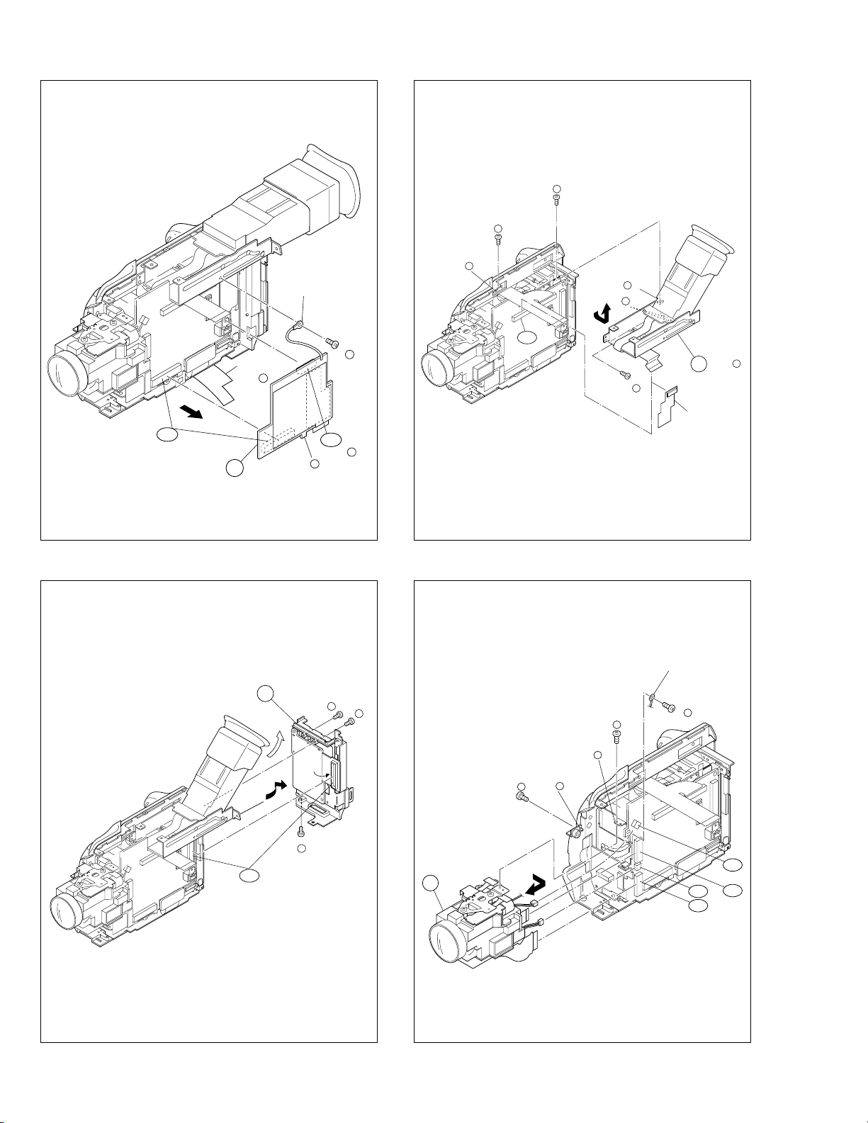
1. DISASSEMBLY
1.1 BEFORE ASSEMBLY AND DISASSEMBLY ......................... 1-1
1.1.1 Precautions..................................................................... 1-1
1.1.2 Assembly and disassembly ............................................ 1-1
1.1.3 Destination of connectors ............................................... 1-1
1.1.4 Disconnection of Connectors (Wires) ............................. 1-1
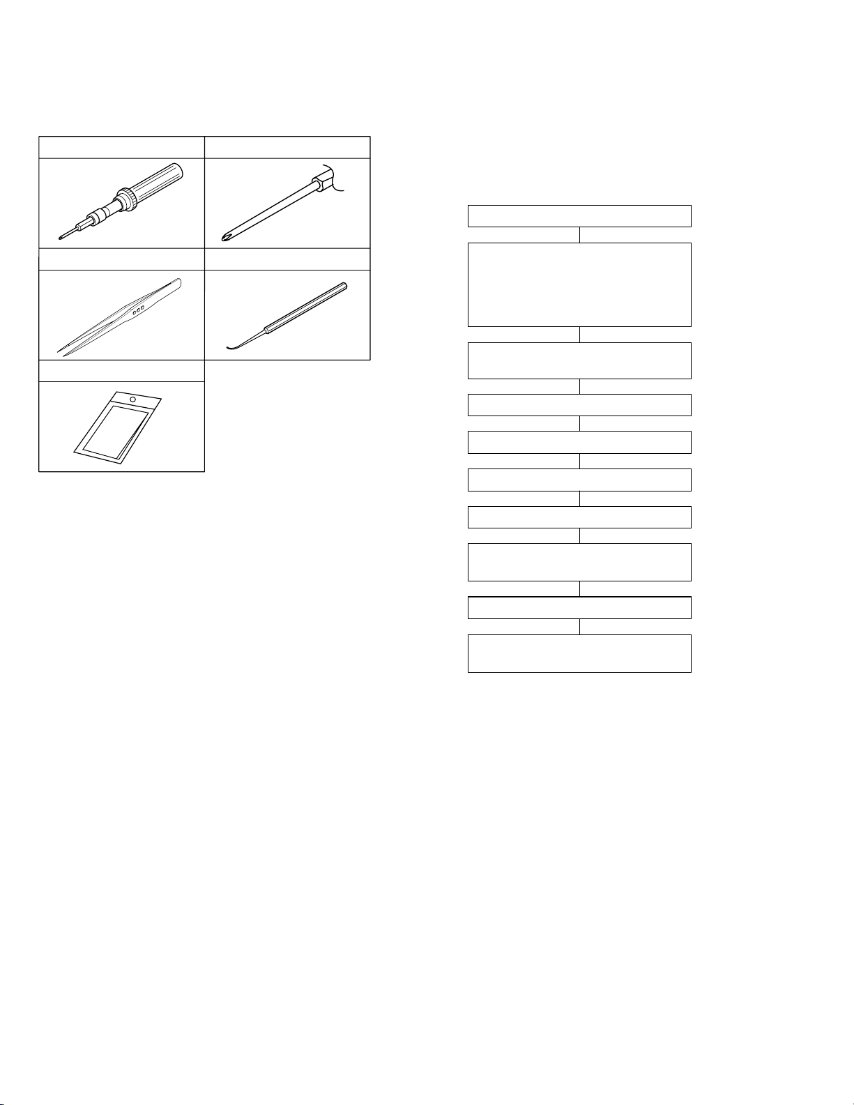
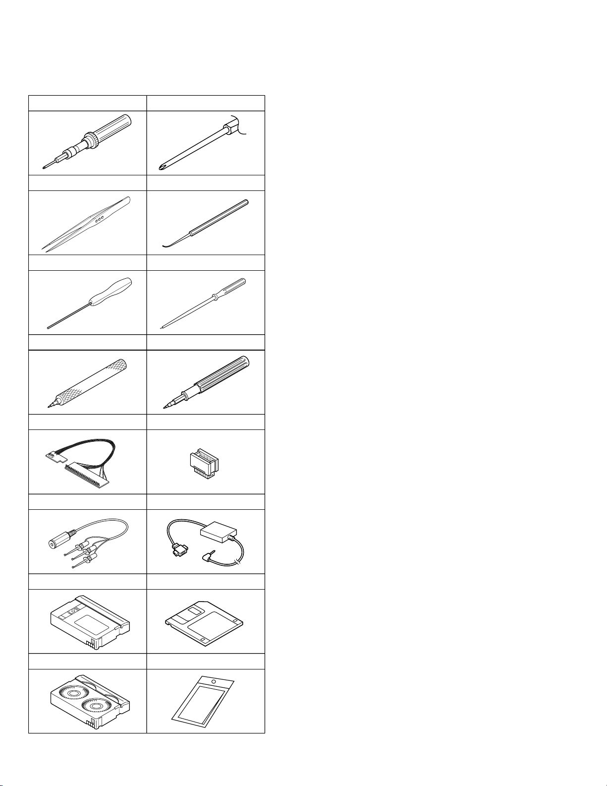
1.2 JIGS AND TOOLS REQUIRED FOR DISASSEMBLY,
ASSEMBLY AND ADJUSTMENT .......................................... 1-2
1.2.1 Tools required for adjustments ....................................... 1-2
1.3 DISASSEMBLY/ASSEMBLY OF CABINET PARTS AND
BOARD ASSEMBLY .............................................................. 1-2
1.3.1 Disassembly flow chart ................................................... 1-2
1.3.2 Disassembly method ...................................................... 1-3
1.4 E.VF(COLOR) ....................................................................... 1-8
1.4.1. Disassembly/Assembly of the 6 E.VF(COLOR) ............ 1-8
DISASSEMBLY OF THE 7 OP BLOCK AND CCD BOARD ASSEMBLIES
1.5
1.5.1 Precautions..................................................................... 1-9
1.5.2 How to remove ............................................................... 1-9
1.5.3 How to install .................................................................. 1-9
1.5.4 Replacement of Service Repair Parts ............................ 1-9
1.6
DISASSEMBLY/ASSEMBLY OF THE @ MONITOR ASSEMBLY ...
1.6.1 @ Monitor Assembly and Hinge Assembly ................... 1-10
1.7 MANUAL EJECTION OF THE CASSETTE TAPE ................ 1-11
1.8 EMERGENCY DISPLAY ...................................................... 1-12
1.9 SERVICE NOTE .................................................................. 1-13
2. MECHANISM ADJUSTMENT
2.1
PRELIMINARY REMARKS ON ADJUSTMENT AND REPAIR ....
2.1.1 Precautions..................................................................... 2-1
2.1.2 Notes on procedure for disassemby/assembly............... 2-1
2.2 JIGS AND TOOLS REQUIRED FOR DISASSEMBLY,
ASSEMBLY AND ADJUSTMENT .......................................... 2-2
2.2.1 Tools required for adjustments ....................................... 2-2
2.3 DISASSEMBLY/ASSEMBLY OF MECHANISM ASSEMBLY . 2-3
2.3.1 General statement .......................................................... 2-3
2.3.2 Explanation of mechanism mode ................................... 2-3
2.3.3 Mechanism timing chart.................................................. 2-4
2.4 DISASSEMBLING PROCEDURE TABLE ............................. 2-5
2.4.1 Disassembly/assembly ................................................... 2-7
2.4.2 List of procedures for disassembly ............................... 2-13
2.5 CHECKUP AND ADJUSTMENT OF MECHANISM PHASE 2-14
2.6 MECHANISM ADJUSTMENTS ........................................... 2-15
2.6.1 Adjustment of the slide guide plate............................... 2-15
2.6.2
Adjustment of the Tension Arm and Pad Arm Assemblies .
2.6.3 Adjustment of the Slide Lever 2.................................... 2-16
2.7 JIG CONNECTOR CABLE CONNECTION ......................... 2-17
2.8 SERVICE NOTE .................................................................. 2-18
3. ELECTRICAL ADJUSTMENT
3.1 PRECAUTION ....................................................................... 3-1
3.2 SETUP ................................................................................... 3-2
3.3 MONITOR ADJUSTMENT ..................................................... 3-3
3.3.1 PLL (MONI)..................................................................... 3-3
3.4 ELECTRONIC VIEWFINDER (E.VF) ADJUSTMENT ............ 3-3
3.4.1 PLL (VF) ......................................................................... 3-3
1-9
1-10
2-1
2-16
4. CHARTS AND DIAGRAMS
NOTES OF SCHEMATIC DIAGRAM .......................................... 4-1
CIRCUIT BOARD NOTES ........................................................... 4-2
4.1 BOARD INTERCONNECTIONS ........................................... 4-3
4.2 MAIN IF SCHEMATIC DIAGRAM (1/2) ................................. 4-5
4.3 MAIN IF SCHEMATIC DIAGRAM (2/2) ................................. 4-7
4.4 CPU SCHEMATIC DIAGRAM ............................................... 4-9
4.5 MSD CPU SCHEMATIC DIAGRAM .................................... 4-11
4.6 DV MAIN SCHEMATIC DIAGRAM ..................................... 4-13
4.7 V OUT SCHEMATIC DIAGRAM ......................................... 4-15
4.8 ANA IN SCHEMATIC DIAGRAM [GR-DV2000EG/EK] ....... 4-17
4.9 TG/VDR SCHEMATIC DIAGRAM ....................................... 4-19
4.10 CDS/AD SCHEMATIC DIAGRAM .................................... 4-21
4.11 DSP SCHEMATIC DIAGRAM .......................................... 4-23
4.12 OP DRIVE SCHEMATIC DIAGRAM ................................ 4-25
4.13 DSC SCHEMATIC DIAGRAM .......................................... 4-27
4.14 P SHIFT SCHEMATIC DIAGRAM ................................... 4-29
4.15 USB SCHEMATIC DIAGRAM .......................................... 4-31
4.16 DSC IF SCHEMATIC DIAGRAM ..................................... 4-33
4.17 MDA SCHEMATIC DIAGRAM ......................................... 4-35
4.18 PRE/REC SCHEMATIC DIAGRAM ................................. 4-37
4.19 AUDIO SCHEMATIC DIAGRAM ...................................... 4-39
4.20 REG SCHEMATIC DIAGRAM .......................................... 4-41
4.21 MONITOR SCHEMATIC DIAGRAM ................................ 4-43
4.22 JACK SCHEMATIC DIAGRAM ........................................ 4-45
4.23 EJECT AND DECK OPE. SCHEMATIC DIAGRAMS ...... 4-47
4.24 CCD SCHEMATIC DIAGRAM .......................................... 4-48
4.25 ZOOM OPE. UNIT, POWER OPE. UNIT,
SUB OPE. UNIT, MENU SW UNIT AND
FRONT FPC UNIT SCHEMATIC DIAGRAMS ................. 4-49
4.26 MAIN CIRCUIT BOARD ................................................... 4-51
4.27 DSC CIRCUIT BOARD .................................................... 4-57
4.28 PRE/MDA CIRCUIT BOARD ............................................ 4-59
4.29 AUDIO CIRCUIT BOARD................................................. 4-61
4.30 REG CIRCUIT BOARD .................................................... 4-63
4.31 MONITOR CIRCUIT BOARD ........................................... 4-65
4.32 JACK CIRCUIT BOARD ................................................... 4-67
4.33 EJECT AND DECK OPE. CIRCUIT BOARDS ................. 4-69
4.34 CCD CIRCUIT BOARD .................................................... 4-71
4.35 VOLTAGE CHARTS ......................................................... 4-72
4.36 POWER SYSTEM BLOCK DIAGRAM ............................. 4-77
4.37 REGULATOR SYSTEM BLOCK DIAGRAM .................... 4-79
4.38 VIDEO SYSTEM BLOCK DIAGRAM ............................... 4-81
4.39 AUDIO SYSTEM BLOCK DIAGRAM ............................... 4-85
5. PARTS LIST
5.1 PACKING AND ACCESSORY ASSEMBLY <M1> ................ 5-1
5.2 FINAL ASSEMBLY <M2> ...................................................... 5-3
5.3 MECHANISM ASSEMBLY <M3>.......................................... 5-6
5.4 ELECTRONIC VIEWFINDER ASSEMBLY <M4> ................. 5-8
5.5 MONITOR ASSEMBLY <M5> ............................................... 5-9
5.6 ELECTRICAL PARTS LIST ................................................. 5-10
MAIN BOARD ASSEMBLY <01> ............................................. 5-10
DSC BOARD ASSEMBLY <02> .............................................. 5-18
PRE/MDA BOARD ASSEMBLY <03> ..................................... 5-20
AUDIO BOARD ASSEMBLY <04> .......................................... 5-21
REG BOARD ASSEMBLY <05> .............................................. 5-23
MONITOR BOARD ASSEMBLY <06> ..................................... 5-24
JACK BOARD ASSEMBLY <07> ............................................ 5-25
EJECT BOARD ASSEMBLY <08> .......................................... 5-26
DECK OPE. BOARD ASSEMBLY <09> .................................. 5-26
CCD BOARD ASSEMBLY <10> .............................................. 5-26
The following table lists the differing points between Models GR-DV1800EG/EK and GR-DV2000EG/EK in this serise.
GR-DV1800EG GR-DV1800EK GR-DV2000EG GR-DV2000EK
AV INPUT NOT USED USED
S INPUT/OUTPUT NOT USED/USED(JACK BOX) USED/USED(JACK BOX)
DV INPUT NOT USED USED
AC ADAPTOR CHARGER AA-V40EG AA-V40EK AA-V40EG AA-V40EK
Page 3
Important Safety Precautions
Prior to shipment from the factory, JVC products are strictly inspected to conform with the recognized product safety and electrical codes of the
countries in which they are to be sold. However, in order to maintain such compliance, it is equally important to implement the following precautions
when a set is being serviced.
Precautions during Servicing
•
1. Locations requiring special caution are denoted by labels and inscriptions on the cabinet, chassis and certain parts of the product.
When performing service, be sure to read and comply with these
and other cautionary notices appearing in the operation and service manuals.
2. Parts identified by the ! symbol and shaded ( ) parts are
critical for safety.
Replace only with specified part numbers.
Note: Parts in this category also include those specified to com-
ply with X-ray emission standards for products using
cathode ray tubes and those specified for compliance
with various regulations regarding spurious radiation
emission.
3. Fuse replacement caution notice.
Caution for continued protection against fire hazard.
Replace only with same type and rated fuse(s) as specified.
4. Use specified internal wiring. Note especially:
1) Wires covered with PVC tubing
2) Double insulated wires
3) High voltage leads
5. Use specified insulating materials for hazardous live parts. Note
especially:
1) Insulation Tape 3) Spacers 5) Barrier
2) PVC tubing 4) Insulation sheets for transistors
6. When replacing AC primary side components (transformers, power
cords, noise blocking capacitors, etc.) wrap ends of wires securely
about the terminals before soldering.
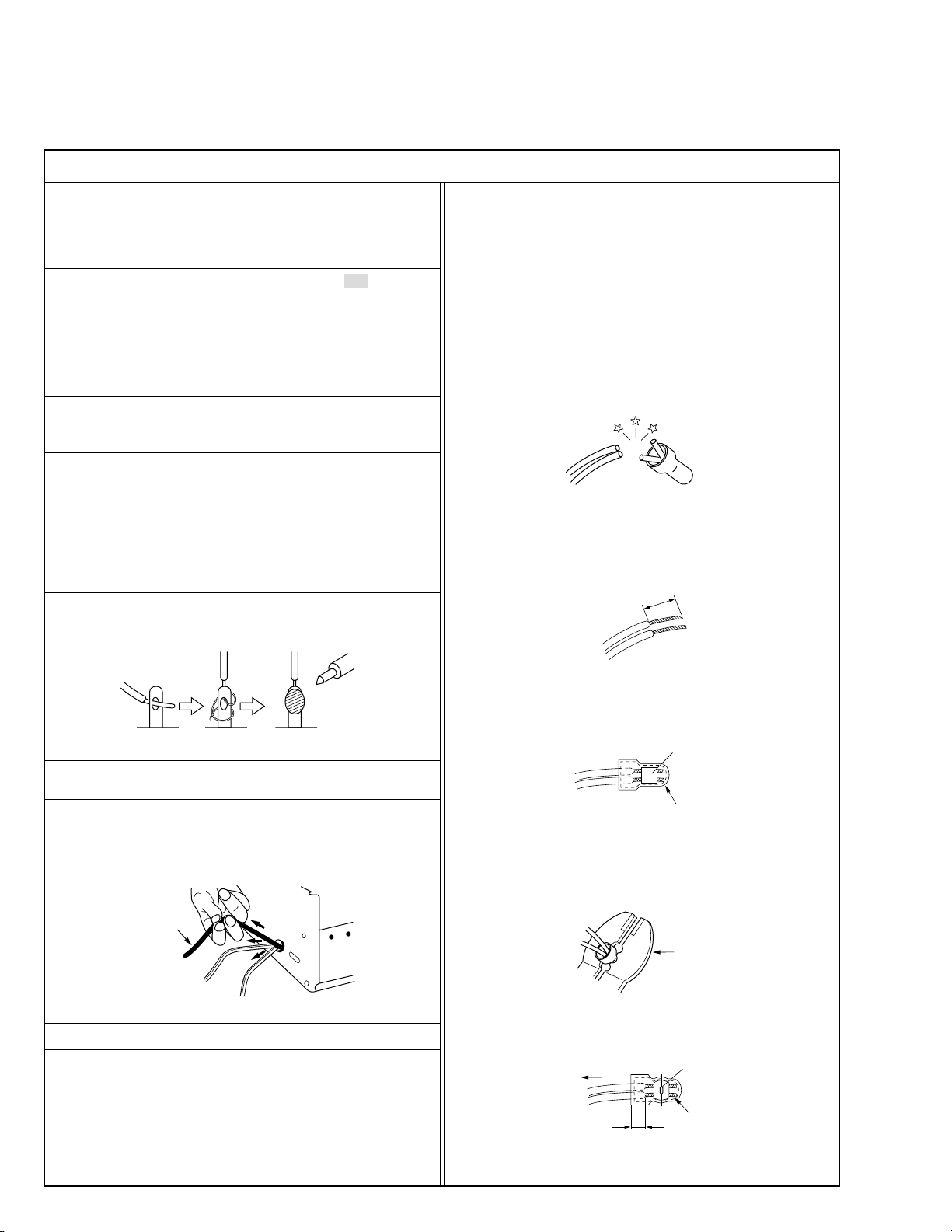
12. Crimp type wire connector
In such cases as when replacing the power transformer in sets
where the connections between the power cord and power transformer primary lead wires are performed using crimp type connectors, if replacing the connectors is unavoidable, in order to prevent
safety hazards, perform carefully and precisely according to the
following steps.
1) Connector part number : E03830-001
2) Required tool : Connector crimping tool of the proper type which
will not damage insulated parts.
3) Replacement procedure
(1) Remove the old connector by cutting the wires at a point
close to the connector.
Important : Do not reuse a connector (discard it).
cut close to connector
Fig.3
(2) Strip about 15 mm of the insulation from the ends of the
wires. If the wires are stranded, twist the strands to avoid
frayed conductors.
15 mm
Fig.1
7. Observe that wires do not contact heat producing parts (heatsinks,
oxide metal film resistors, fusible resistors, etc.)
8. Check that replaced wires do not contact sharp edged or pointed
parts.
9. When a power cord has been replaced, check that 10-15 kg of
force in any direction will not loosen it.
Power cord
Fig.2
10. Also check areas surrounding repaired locations.
11. Products using cathode ray tubes (CRTs)
In regard to such products, the cathode ray tubes themselves, the
high voltage circuits, and related circuits are specified for compliance with recognized codes pertaining to X-ray emission.
Consequently, when servicing these products, replace the cathode ray tubes and other parts with only the specified parts. Under
no circumstances attempt to modify these circuits.
Unauthorized modification can increase the high voltage value and
cause X-ray emission from the cathode ray tube.
Fig.4
(3) Align the lengths of the wires to be connected. Insert the
wires fully into the connector.
Metal sleeve
Connector
Fig.5
(4) As shown in Fig.6, use the crimping tool to crimp the metal
sleeve at the center position. Be sure to crimp fully to the
complete closure of the tool.
1
.2
5
2
.0
5
.5
Fig.6
(5) Check the four points noted in Fig.7.
Not easily pulled free
Wire insulation recessed
more than 4 mm
Fig.7
Crimping tool
Crimped at approx. center
of metal sleeve
Conductors extended
I
S40888-01
Page 4
Safety Check after Servicing
•
Examine the area surrounding the repaired location for damage or deterioration. Observe that screws, parts and wires have been returned
to original positions, Afterwards, perform the following tests and confirm the specified values in order to verify compliance with safety
standards.
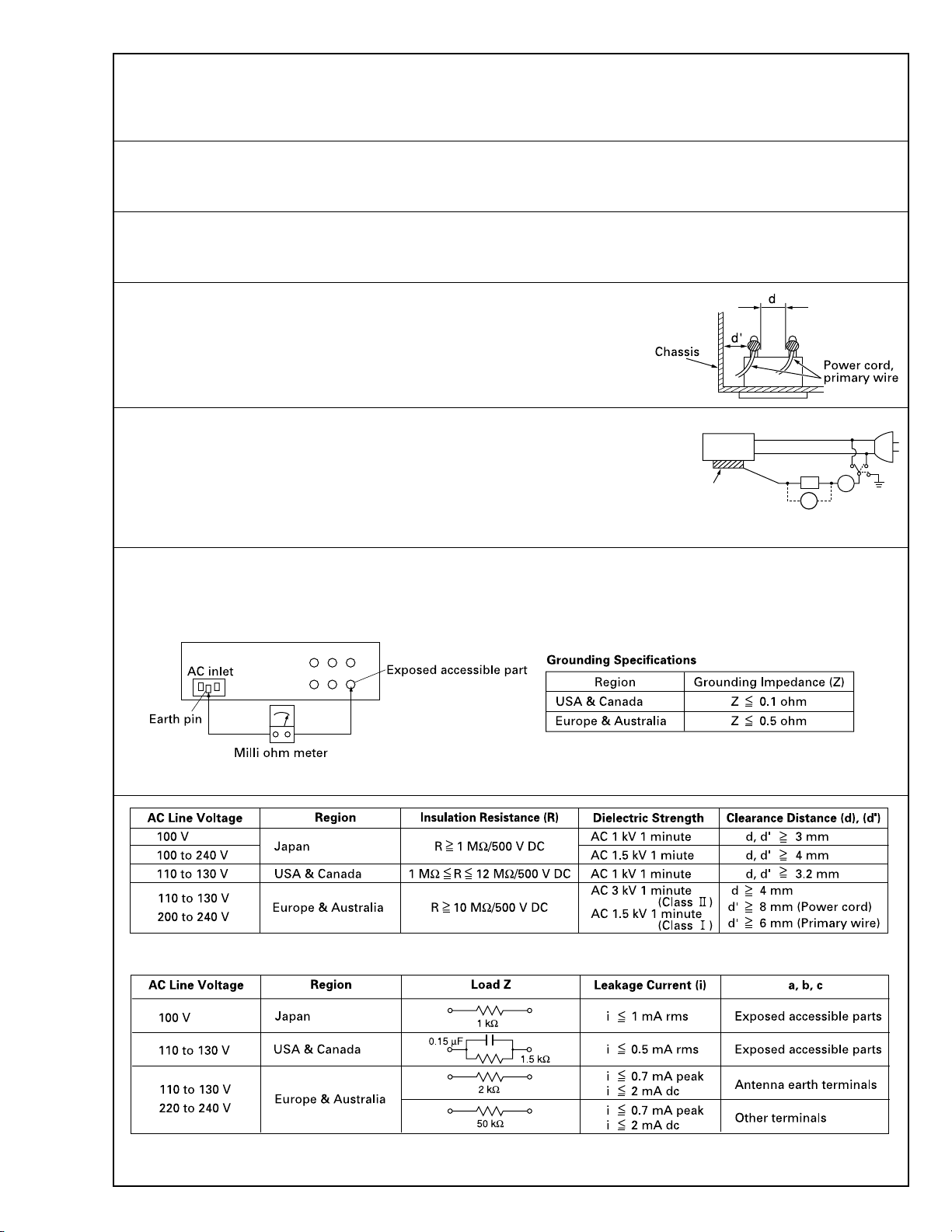
1. Insulation resistance test
Confirm the specified insulation resistance or greater between power cord plug prongs and externally exposed parts of the set (RF terminals, antenna terminals, video and audio input and output
terminals, microphone jacks, earphone jacks, etc.). See table 1 below.
2. Dielectric strength test
Confirm specified dielectric strength or greater between power cord plug prongs and exposed accessible parts of the set (RF terminals, antenna terminals, video and audio input and output terminals,
microphone jacks, earphone jacks, etc.). See table 1 below.
3. Clearance distance
When replacing primary circuit components, confirm specified clearance distance (d), (d’) between soldered terminals, and between terminals and surrounding metallic parts. See table 1
below.
Fig. 8
4. Leakage current test
Confirm specified or lower leakage current between earth ground/power cord plug prongs and
externally exposed accessible parts (RF terminals, antenna terminals, video and audio input and
output terminals, microphone jacks, earphone jacks, etc.).
Measuring Method : (Power ON)
Insert load Z between earth ground/power cord plug prongs and externally exposed accessible
parts. Use an AC voltmeter to measure across both terminals of load Z. See figure 9 and following
table 2.
Externally
exposed
accessible part
Fig. 9
Z
V
ab
A
c
5. Grounding (Class 1 model only)
Confirm specified or lower grounding impedance between earth pin in AC inlet and externally exposed accessible parts (Video in, Video out,
Audio in, Audio out or Fixing screw etc.).
Measuring Method:
Connect milli ohm meter between earth pin in AC inlet and exposed accessible parts. See figure 10 and grounding specifications.
Fig. 10
Table 1 Specifications for each region
Table 2 Leakage current specifications for each region
Note: These tables are unofficial and for reference only. Be sure to confirm the precise values for your particular country and locality.
II
S40888-01
Page 5

Page 6
SECTION 1
DISASSEMBLY
1.1 BEFORE ASSEMBLY AND DISASSEMBLY
1.1.1 Precautions
1. Be sure to remove the power supply unit prior to mounting and soldering of parts.
2. When removing a component part that needs to disconnect the connector and to remove the screw for removing itself, first disconnect the connecting wire from the
connector and then remove the screw beforehand.
3. When connecting and disconnecting the connectors, be
careful not to damage the wire.
4. Carefully remove and handle the part to which some
spacer or shield is attached for reinforcement or insulation.
5. When replacing chip parts (especially IC parts), desolder
completely first (to prevent peeling of the pattern).
6. Tighten screws properly during the procedures.
Unless specified otherwise, tighten screws at a torque
of 0.069N
•
m(0.7kgf•cm).
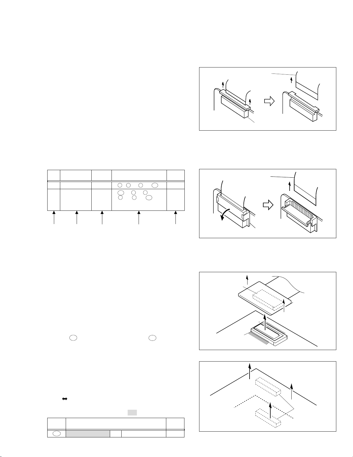
1.1.2 Assembly and disassembly
STEP
No.
1
2
PART
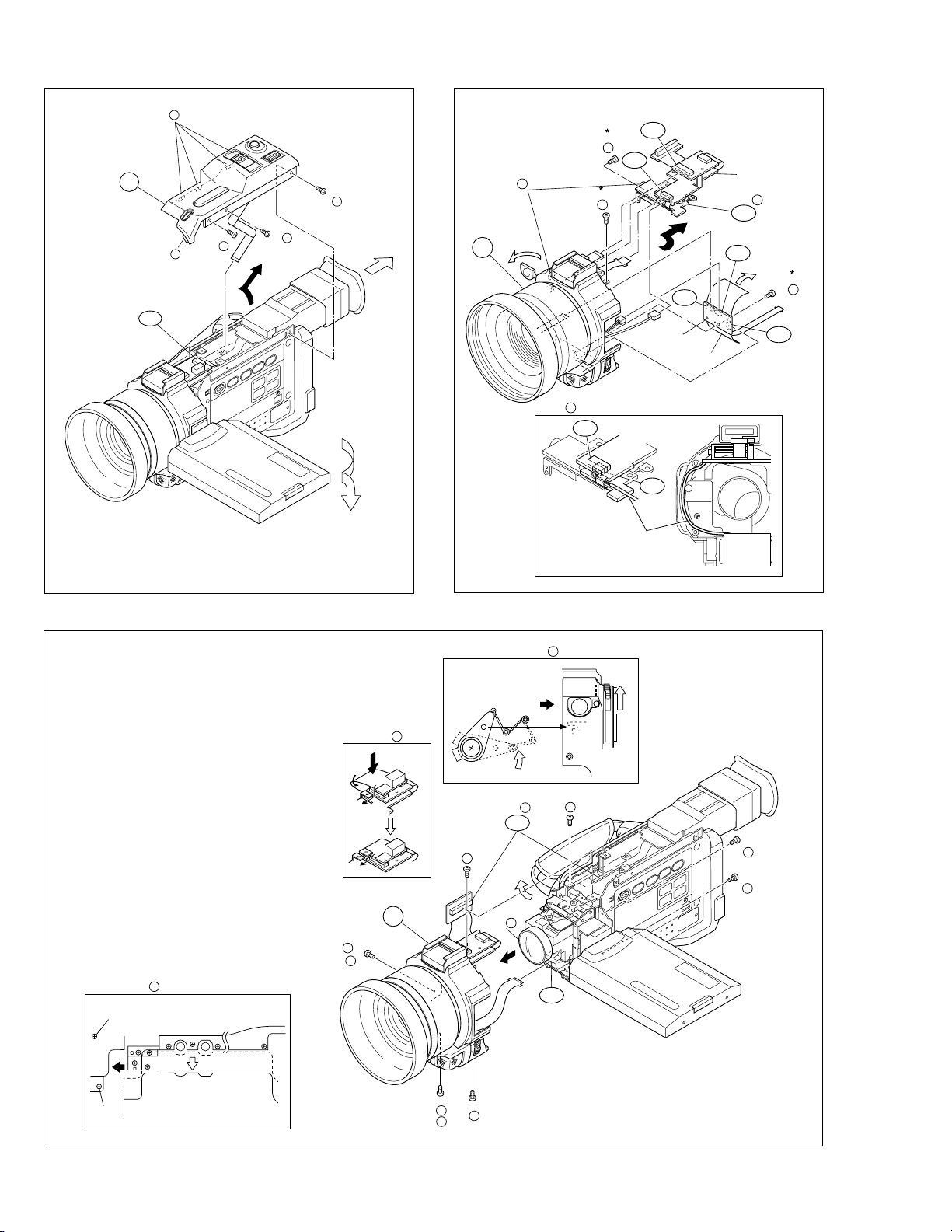
ZOOM OPE UNIT Fig.1-3-1
FRONT COVER Fig.1-3-2 CN 2a ,2(S 2 a),(S 2 b), NOTE2a
ASSY 2(S 2 c),2(S 2 b),CN 2b NOTE2b
Fig.No.
POINT NOTE
3(S 1 ),(L 1 a),4(L 1 b),CN 1a
–
NOTE2c
NOTE2d
1.1.4 Disconnection of Connectors (Wires)
Connector
Pull both ends of the connector in the arrow direction, remove the lock and disconnect the flat wire.
Flat wire
Connector
Fig. 1-1-1 Connector 1
Extend the locks in the direction of the arrow for unlocking
and then pull out the wire. After removing the wire, immediately restore the locks to their original positions because
the locks are apt to come off the connector.
Flat wire
(1) (2) (3) (4) (5)
(1) Indicate the disassembly steps. When assembling, per-
form in the reverse order of these steps. This number
corresponds to the number in the disassembly diagram.
(2) Indicates the name of disassembly/assembly parts.
(3) Indicates the number in the disassembly diagram.
(4) Indicates parts and points such as screws, washers,
springs which must be removed during disassembly/
assembly.
Symbol Name, Point
S Screw
L Lock, Pawl, Hook
SD Soldering
夡(Others) Connector, Cover, Bracket, etc.
(Example)
• 2 (S1) : Remove the two screws (S1) for removing
the part 1.
• CN 1a : Disconnect the connector 1a .
•SD1 : Unsolder at the point SD1.
(5) Precautions on disassembly/assembly.
1.1.3 Destination of connectors
Note:
Three kinds of double-arrows in connection tables respectively show kinds of connector/wires.
↔ : Wire
⇔ : Flat wire
: Board to Board connector
[Example]
Note:
Remove the parts marked in .
CONN.
No.
1a AUDIO CN203 ⇔ ZOOM OPE – 8
CONNECTOR
Pin No.
Connector
Fig. 1-1-2 Connector 2
B-B connector
Pull the board by both the sides in the direction of the arrow for disconnecting the B-B connector.
Connector
Connector
Fig. 1-1-3 Connector 3
Connector
Fig. 1-1-4 Connector 4
1-1
Page 7
1.2 JIGS AND TOOLS REQUIRED FOR DISASSEMBLY, ASSEMBLY AND ADJUSTMENT
1.2.1 Tools required for adjustments
1
Torque Driver
YTU94088
2
Bit
YTU94088-003
1.3 DISASSEMBLY/ASSEMBLY OF CABINET PARTS AND BOARD ASSEMBLY
1.3.1 Disassembly flow chart
This flowchart indicates the disassembly step for the cabinet parts and board assembly in order to gain access to
item(s) to be serviced. When reassembling, perform the
step(s) in reverse order.
3
5
Tweezers
P-895
Cleaning Cloth
KSMM-01
Chip IC Replacement Jig
4
PTS40844-2
Table 1-2-1
1. Torque driver
Be sure to use to fastening the mechanism and exterior
parts because those parts must strictly be controlled for
tightening torque.
2. Bit
This bit is slightly longer than those set in conventional
torque drivers.
3. Tweezers
To be used for removing and installing parts and wires.
4. Chip IC replacement jig
To be used for adjustment of the camera system.
5. Cleaning cloth
Recommended cleaning cloth to wipe down the video
heads, mechanism (tape transport system), optical lens
surface.
1
2
ZOOM OPE UNIT
FRONT COVER ASSY
(Inc. AUDIO BOARD ASSY,
FRONT FPC UNIT,
MICROPHONE,
SHOE ASSY)
3
4
5
6
7
8
9
0
/
!
UPPER CASE ASSY
(Inc.
MONITOR ASSY)
@
DSC BOARD ASSY
REAR COVER ASSY
E. VF(COLOR)
OP BLOCK ASSY
LOWER CASE ASSY
(Inc.JACK,EJECT BOARD ASSY)
MAIN BOARD ASSY
PRE/MDA BOARD ASSY,
MECHANISM ASSY
Table 1-3-1
1-2
Page 8
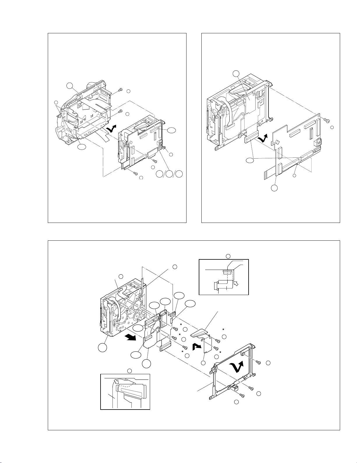
1.3.2 Disassembly method
STEP
No.
1
2
3
4
5
6
7
8
9
0
/ ASSY, 2(S 10 b), NOTE0b
!
PART
ZOOM OPE UNIT Fig.1-3-1
FRONT COVER Fig.1-3-2 CN 2a ,2(S 2 a),(S 2 b), NOTE2a
ASSY 2(S 2 c),2(S 2 b),CN 2b NOTE2b
--------------------------------------------------------
AUDIO BOARD ASSY
-------------- ---------------------------------
FRONT FPC UNIT
--------------------------------------------------------
MICROPHONE Fig.1-3-2c 2(S 2 f),(S 2 g),2(S 2 h),2(L 2 a)
-------------- ---------------------------------
SHOE ASSY SPACER,2(L 2 b) NOTE2j
UPPER CASE ASSY
Inc. MONITOR CN 3a NOTE3b
ASSY NOTE3c
DSC BOARD ASSY
REAR COVER ASSY
E.VF(COLOR) Fig.1-3-6
OP BLOCK ASSY Fig.1-3-7 (S 7 a),LUG WIRE,CN 7a , –
LOWER CASE Fig.1-3-8 CN 8a ,CN 8b ,3(S 8 a), –
ASSY (S 8 b),2(L 8 a),(L 8 b)
MAIN BOARD ASSY
PRE/MDA BOARD
MECHANISM
ASSY CN 10a ,CN 10b ,CN 10c ,
Fig.No.
3(S 1 ),(L 1 a),4(L 1 b),CN 1a
Fig.1-3-2b CN 2c ,(S 2 d),(S 2 e),CN 2d ), NOTE2e
CN 2e ) NOTE2f
SPACER,CN 2f ,CN 2g ,CN 2h ,
(S 2 e)
Fig.1-3-3 3(S 3 a),6(S 3 b),(S 3 c), NOTE3a
Fig.1-3-4 (S 4 ),LUG WIRE,HEAT SINK, NOTE4a
(L 4 ),CN 4a ,CN 4b NOTE4b
Fig.1-3-5 CN 5a ,2(S 5 a),(S 5 b) –
HEAT SINK(MAIN),CN 6a ,(S 6 a),
2(S 6 b),(L 6 a),(L 6 b),2(L 6 c)
CN 7b ,CN 7c ,CN 7d ,2(S 7 b),
(L 7 a),(L 7 b)
Fig.1-3-9 CN 9a ,(S 9 ),(L 9 ) –
Fig.1-3-10 3(S 10 a),BKT(MECHA) ASSY, NOTE0a
(L 10 ),SHIELD COVER(PRE/REC),
CN 10d ,CN 10e ,CN 10f ,
3(S 10 b)
POINT NOTE
Table 1-3-2
Note:
Remove the parts marked in .
CONN.
No.
1a AUDIO CN203 ⇔ ZOOM OPE – 8
2a AUDIO CN201 MAIN CN112 80
2b EJECT CN2421 ⇔ FRONT FPC – 12
2c AUDIO CN202 ⇔ SHOE ASSY – 16
2d AUDIO CN205 ⇔ LENS SHUTTER – 10
2e AUDIO CN204 ↔ MICROPHONE – 3
2f
FRONT FPC UNIT
2g
FRONT FPC UNIT CN2412
2g FRONT FPC UNIT CN2411
3a MAIN CN108 MONITOR – 50
4a DSC CN8401 MAIN CN105 120
4b DSC CN8402 ⇔ JACK CN301 20/45
5a MAIN CN109 REG CN601 80
6a MAIN CN110 ⇔ E.VF(COLOR) CN501 22
7a MAIN CN102 ⇔ CCD – 20
7b MAIN CN101 ↔ CCD – 2
7c MAIN CN103 ↔ OP BLOCK ASSY – 2
7d MAIN CN104 ⇔ OB BLOCK ASSY – 39
8a EJECT CN2422 ⇔ MAIN CN113 13
8b JACK CN301 ⇔ MAIN CN111 24/45
9a MAIN CN106 PRE/MDA CN401 80
10a PRE/MDA CN406 ⇔ SENSOR – 16
10b PRE/MDA CN405 ⇔
10c PRE/MDA CN404 ⇔ DRUM MOTOR – 11
10d PRE/MDA CN402 ⇔ HEAD – 8
10e PRE/MDA CN407 ⇔
10f PRE/MDA CN403 ⇔
CONNECTOR
CN2413 ⇔ FOCUS RING – 6
↔
IR UNIT
⇔
MENU SW UNIT
CAPSTAN .MOTOR
ROTARY ENCODER
LOADING MOTOR
–
–
– 18
– 6
– 6
–
NOTE2c
NOTE2d
–
NOTE2g
NOTE2h
NOTE6
Pin No.
3
6
NOTE 2a:
Open the cassette cover after removing the
screws.
NOTE 2b:
Be careful not to damage the FPC when unplugging it.
NOTE 2c:
As the
result of the above steps, be careful not to damage any of its parts. Take particular care not to
scratch the lens surfaces.
NOTE 2d:
When mounting the parts, set the REC MODE
switch to “video”. Also set the lever to the uppermost position at the same time.
NOTE 2e:
NOTE 2f:
Treat the microphone wire with care.
When mounting, be careful not to damage the
jacks.
NOTE 2g:
When mounting, be careful not to damage the
switches.
NOTE 2h:
When mounting, be careful when handling the
FPC.
NOTE 2j:
When mounting, be careful not to damage the
boss (stud).
NOTE 3a/3b:
NOTE 3c:
For the disassembly of the
bly, see section 1.6, “Disassembly/Assembly of
@
NOTE 4a:
NOTE 4b:
NOTE 6:
NOTE 0a:
NOTE 0b:
Be careful not to damage the CONNECTOR.
Handle the peeled-off heat sink carefully be-
cause it should be reused in the assembly.
For the disassembly of the
1.4, “Disassembly/Assembly of
The FPC of the loading motor should be
mounted by inserting it between the Mechanism
Assembly and the PRE/MDA Board Assembly.
When mounting the shield cover, push down the
FPC of the drum while attaching it.
OP Block Assembly is exposed as a
7
Be sure to confirm the position of the screws.
Monitor Assem-
@
Monitor Assembly”.
E.VF, see section
6
E.VF”.
6
Table 1-3-3
1-3
Page 9
(L b)
NOTE f
2
NOTE e
2
NOTE e
WIRE
(MIC)
2
2d
2d
2
2c
2d
2e
2h
2f
2g
12
(S e)
2
13
(S e)
2
SPACER
FRONT FPC
UNIT
AUDIO BOARD
ASSY
11
(S d)
2
*
: 0.078 N•m (0.8 kgf•cm)
1
1
2
(S )
(L a)
1
1
(S )
1
3
(S )
1
1
1a
Fig. 1-3-1
Fig. 1-3-2b
8
7
NOTE a
2
(BOTTOM)
(S b)
NOTE a
6
2
2
NOTE b
2
2
7
(S c)
2
NOTE a
2
4
(S a)
2
(S c)
NOTE b
NOTE c
8
2
NOTE d
2
2a
2
2
(S a)
2b
VIDEO
XGA/VGA
UXGA
5
2
9
(S d)
2
10
(S d)
2
1-4
Fig. 1-3-2a
Page 10
(
)
NOTE g
2
15
(S f)
2
14
(S f)
2
18
(S h)
2
SWITCH
(S g)
17
(S h)
2
16
2
NOTE h
NOTE j
2
(L b)
2
2
SHOE ASSY
: 0.078 N•m (0.8 kgf•cm)
*
15
(S f)
2
16
(S g)
2
17
(S h)
2
18
(S h)
2
14
(S f)
2
(L a)
2
Fig. 1-3-2c
3a
28
(S c)
3
NOTE 3 b
SPACER
3
NOTE g ,
2
SWITCH
27
(S b)
3
h
2
NOTE 3 b
27
28
15
(S f)
2
FPC
NOTE 3 a
22
20
(S a)
3
21
(S a)
3
22
(S b)
3
NOTE 3 a
19
(S a)
3
(BOTTOM)
25
24
23
26
23
(S b)
3
24
(S b)
3
25
S b
3
12
26
(S b)
3
NOTE 3 c
Fig. 1-3-3
1-5
Page 11
LUG WIRE
(L a)
6
34
(S b)
6
35
(S b)
6
(L b)
(L c)
6
6
4a
Fig. 1-3-4
HEAT SINK
(BASE)
NOTE b
4
29
(S )
4
4
6a
NOTE
6
6
33
(S a)
6
HEAT SINK
(MAIN)
4b
NOTE a
(L )
4
4
Fig. 1-3-6
LUG WIRE
5
30
(S a)
5
31
(S a)
5
38
(S b)
7
36
(S a)
7
1-6
Fig. 1-3-5
(L a)
7
37
(L b)
(S b)
32
(S b)
5
5a
7
7
7
7b
7a
7c
7d
Fig. 1-3-7
Page 12
(
)
(L a)
9
10
9a
43
(S )
9
(L )
9
8
41
(S a)
8
42
(S b)
8
8b
8a
(L b)
8
39
(S a)
8
40
S a
8
9810 11
Fig. 1-3-8 Fig. 1-3-9
NOTE a
10
NOTE a
10
NOTE b
10
10e
10d
10c
10b
11
10a
51
(S b)
10
49
(S b)
10
50
(S b)
10f
10
10
NOTE b
10
FPC
BKT (MECHA) ASSY
CN407
CN403
FPC
SHIELD COVER (PRE/REC)
47
(S b)
10
48
(S b)
10
(L )
10
45
(S a)
10
46
(S a)
10
44
(S a)
10
: 0.078 N•m (0.8 kgf•cm)
*
Fig. 1-3-10
1-7
Page 13
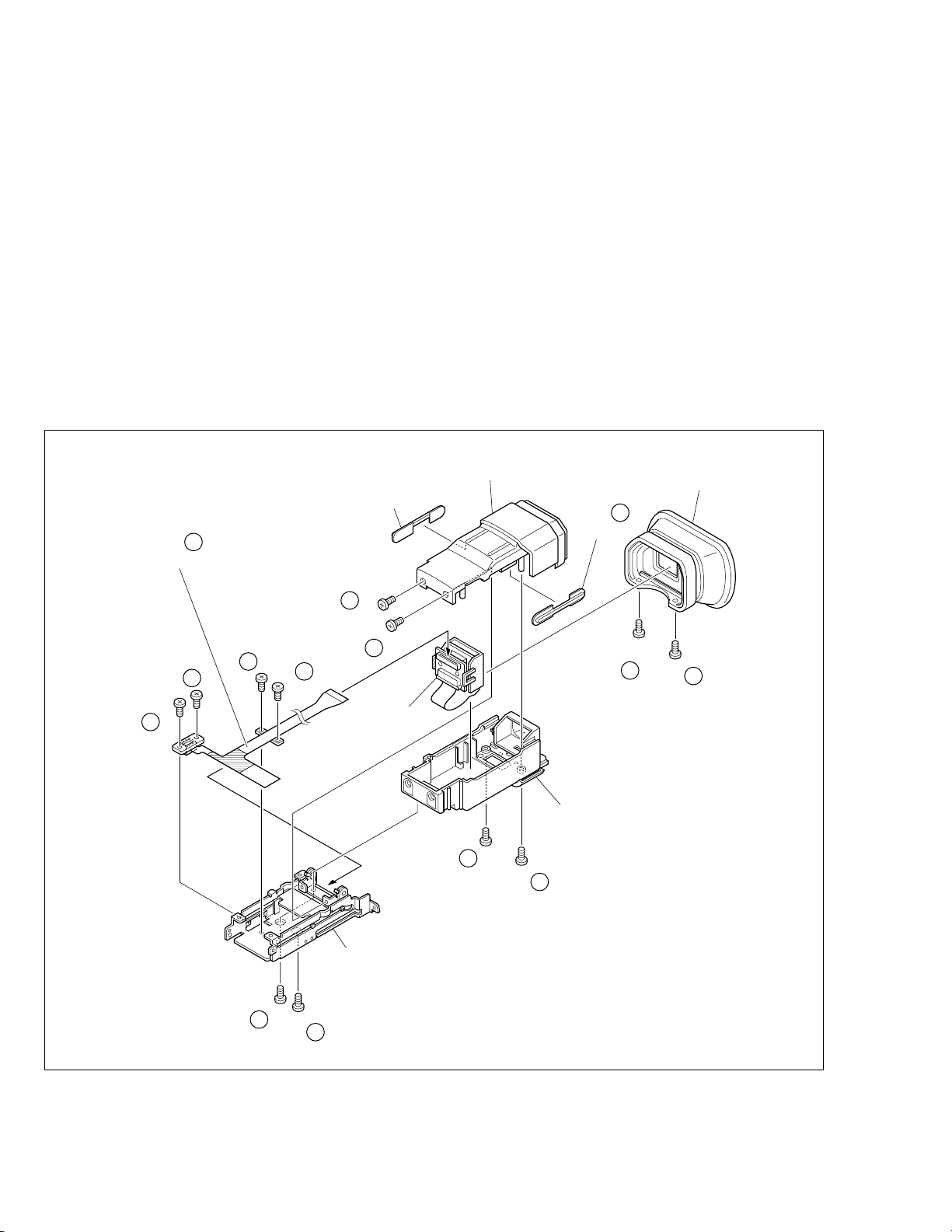
1.46 E.VF(COLOR)
1.4.1. Disassembly/Assembly of the 6 E.VF(COLOR)
1. Remove the 2 screws (1 and 2) and then remove the EYE
CAP.
2. Remove the 2 screws (3 and 4).
3. Pull out the VF assembly and them remove the 4 screws
(5 to 8) to release the FPC ASSY.
4. Remove the 2 screws (9 and 10) then lift the E.VF from
the BRACKET (VF) ASSY and take out the FPC ASSY.
Note
a :
Be careful not to disconnect or break the FPC
6
ASSY wire.
5. Remove the 2 screws (11 and 12) to remove the UPPER
CASE ASSY.
Note
b :
Be careful not to lose any of the parts.
6
6. Remove the LCD UNIT from the BOTTOM CASE ASSY.
NOTE a
FPC ASSY
(S c)
**
5
6
(S c)
**
6
6
6
**
7
6
(S d)
**
8
6
(S d)
**
3
6
(S b)
(S b)
LCD UNIT
**
4
6
RIB
UPPER CASE ASSY
NOTE b
BOTTOM CASE ASSY
**
11
6
(S e)
**
12
6
(S e)
RIB
6
*
1
6
(S a)
EYE CUP
*
2
6
(S a)
1-8
**
9
6
(S e)
BRACKET(VF) ASSY
**
10
6
(S e)
Fig. 1-4-1
: 0.059 N·m (0.6kgf·cm)
*
: 0.078 N·m (0.8kgf·cm)
**
Page 14
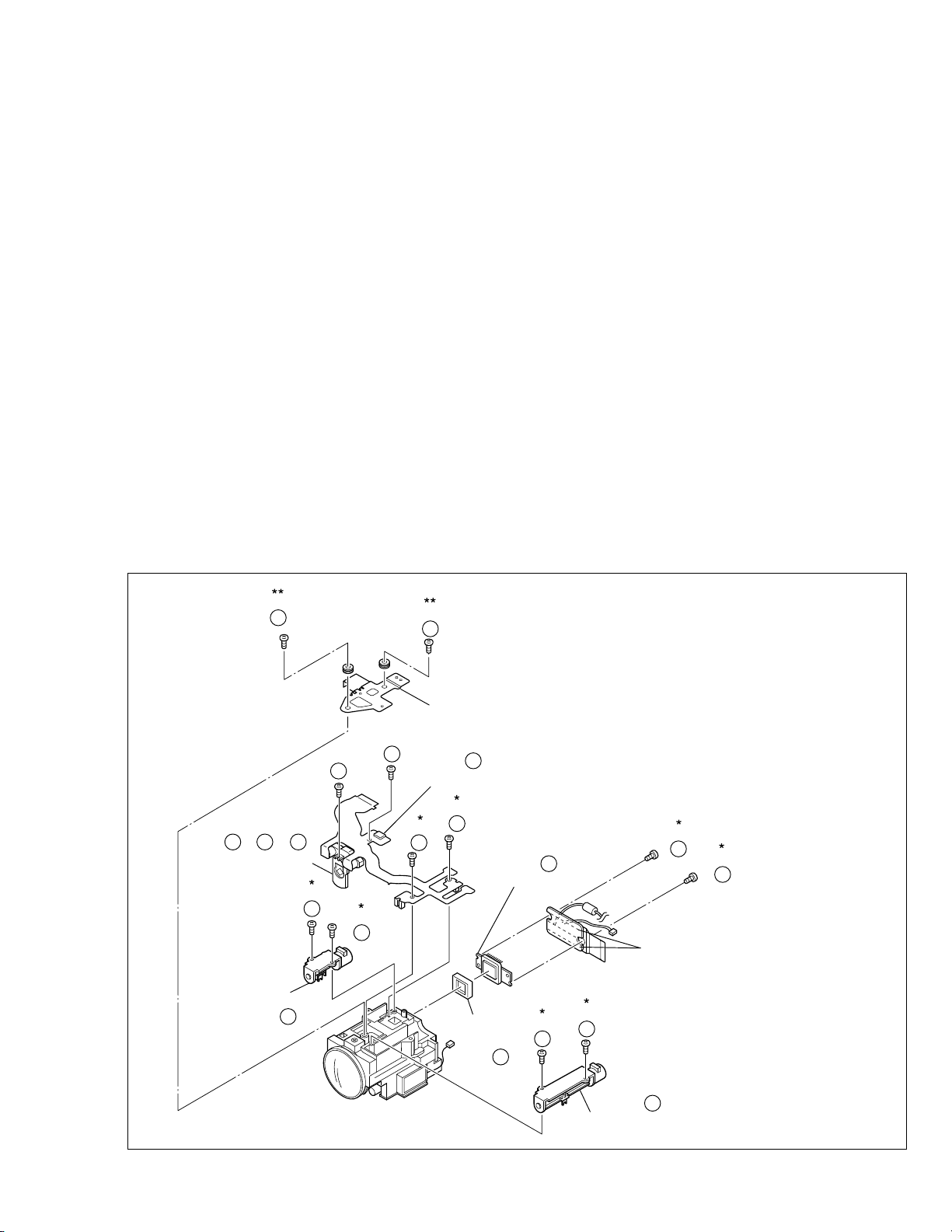
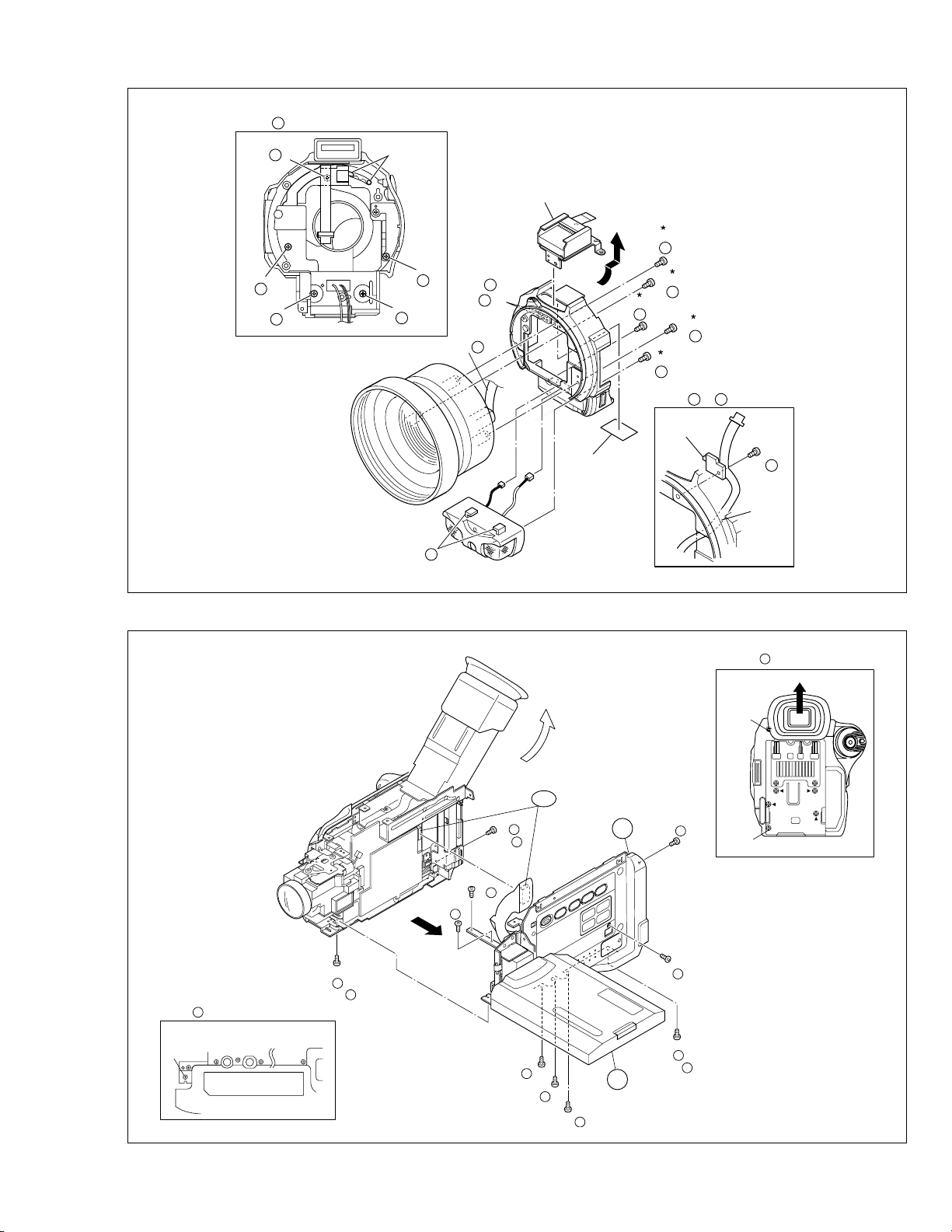
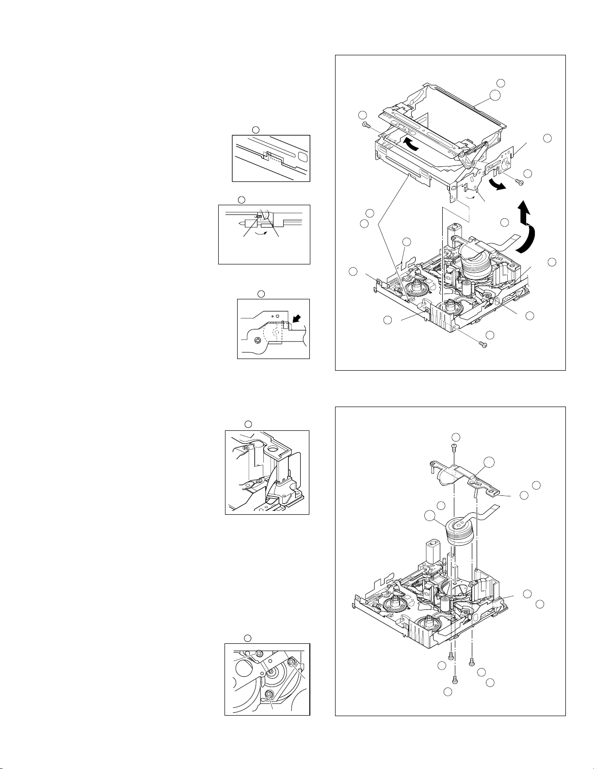
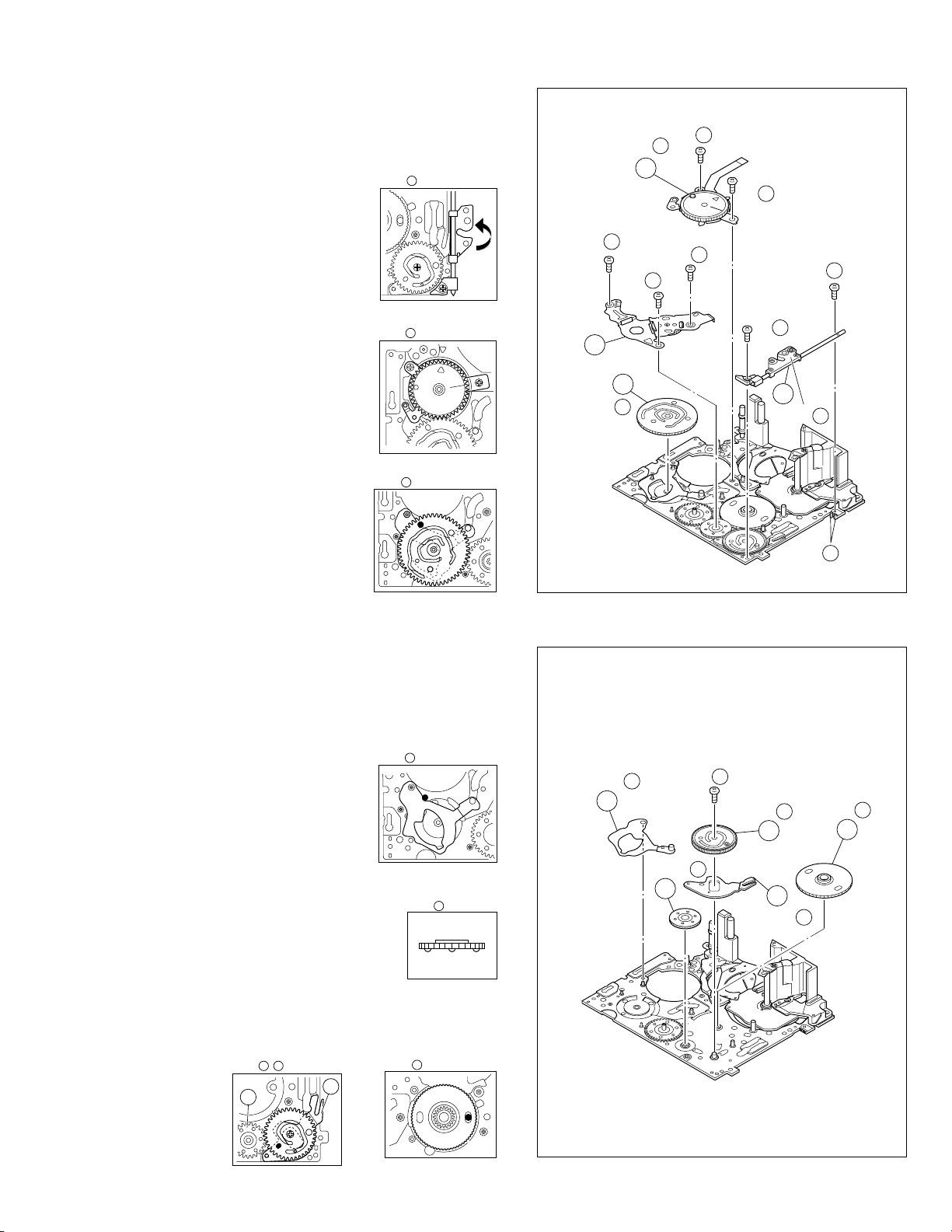
1.5 DISASSEMBLY OF THE 7 OP BLOCK AND CCD BOARD ASSEMBLIES
1.5.1 Precautions
1. Take care in handling the CCD image sensor, optical LPF
and lens components when performing maintenance
etc., especially with regard to surface contamination, attached dust or scratching. If fingerprints are present on
the surface they should be wiped away using either a
silicon paper, clean chamois or the cleaning cloth recommended by the Video Product Division.
2. The CCD image sensor may have been shipped with a
protective sheet attached to the transmitting glass. When
replacing the CCD image sensor, do not peel off this
sheet from the new part until immediately before it is
mounted in the OP Block Assembly.
1.5.3 How to install
1. With the spacer rubbers attached to the CCD base,
mount the CCD base in the OP Block Assembly and
tighten them together using the two screws (1, 2).
2. Mount the CCD Board Assembly and attach solder to
the 16 points (SD1).
1.5.4 Replacement of Service Repair Parts
The service repair parts for the OP Block Assembly are as
listed below.
Before replacement of these parts, remove the bracket (OP
assyembly) as required.
Take special care not to disconnect any of the FPC wires
or cause any damage due to soldering (excessive heating).
1.5.2 How to remove
1. Remove the solder (SD1) from the 16 soldered points
on the CCD Board Assembly and take the assembly out.
2. Remove the two screws (1, 2) and take out the CCD Base
Assembly.
Note
a:
When removing the CCD Base Assembly, be
7
careful not to take out the CCD image sensor together with the spacer rubbers attached to it.
Note 7b:
The CCD image sensor should not be replaced
as a single part but should be replaced together
with the entire CCD Base Assembly.
3
7
(S b)
NOTE 7 c/ 7 d/ 7 e
IRIS MOTOR
UNIT
(S c)
(S c)
9
7
6
7
10
(S c)
(S c)
7
4
7
(S b)
BRACKET (OP) ASSY
5
7
NOTE 7 e
SWITCH
8
7
(S d)
7
7
(S d)
CCD BASE ASSY
1. Focusing motor
2. Zoom motor
3. Iris motor unit
Note
7
Note 7d:
Note 7e:
NOTE 7 b
c:
When replacing the focusing motor or the zoom
motor, solder the FPC at a space of about 1 mm
above the terminal pin.
The iris motor unit includes the FPC Assembly,
switch and two sensors.
Be careful not to damage the switch.
1
7
(S a)
SD1
2
7
(S a)
FOCUS
MOTOR
NOTE 7 c
SPACER
RUBBER
NOTE 7 a
Fig. 1-5-1
11
7
(S c)
12
7
(S c)
NOTE 7 c
ZOOM MOTOR
: 0.118 N·m (1.2kgf·cm)
*
: 0.147 N·m (1.5kgf·cm)
**
1-9
Page 15
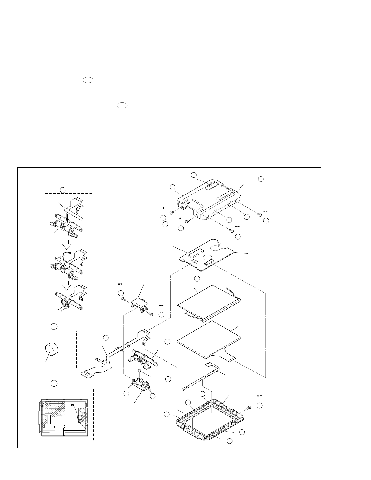
1.6 DISASSEMBLY/ASSEMBLY OF THE @ MONITOR
ASSEMBLY
1.6.1
Monitor Assembly and Hinge Assembly
@
1. Remove the four screws (1 to 4), disengage the four
hooks (L@ a to d) in order, and take out the Monitor Cover
Assembly.
2. Unlock the connector ( 12a ) and, while lifting the Hinge
Assembly, unplug and take out the FPC.
3. Remove the screw (5) and take out the bracket (MONI-
TOR CASE).
4. Unplug the FPC from the connector ( 12b ) and take out
the Monitor Board Assembly and the backlight.
5. Remove the LCD module by disengaging the five hooks
(L@ e to j).
6. Remove the two screws (6, 7) and take out the hinge
covers (U, L) by disengaging the four hooks (L@ k, l) at
both sides of each of the hinge covers.
7. Remove the FPC Assembly from the Hinge Assembly.
12
NOTE f,h
FPC ASSY
(S a)
NOTE a
HINGE
ASSY
(MONITOR CASE)
12
(L a)
1
12
12
(S a)
BRACKET
Note
@
a:
Note @b:
Note @c:
Note @d:
Note @e:
Note @f:
Note @g:
Note @h:
12
(L d)
a
2
12
CN 12b
Don't reuse the screw, because screw lock bond
was applied to them.
Be careful not to damage the FPC or the connector when removing the Monitor Cover Assembly.
Be careful not to damage the parts when removing or mounting the Hinge Assembly.
To unplug the FPC, release only the lock of the
connector and remove the FPC together with the
Hinge Assembly.
As the backlight is soldered at two points on the
Monitor Board Assembly, the solder should be removed when disassembling the backlight as a single part.
Take care when handling the FPC.
Be careful not to lose the magnets and attach
them in the correct orientation.
When mounting the FPC Assembly, wrap it around
the Hinge Assembly by 3-1/2 turns.
12
NOTE b
MONITOR COVER ASSY
4
12
(S b)
MONITOR BOARD ASSY
CN 12a
12
(L b)
(S b)
(L c)
3
12
12
12
NOTE g
MARK (BLACK)
12
NOTE e
WIRE RING
12
NOTE d,f
FPC ASSY
**
HINGE COVER(L)
6
12
(S d)
HINGE ASSY
12
(L k)
HINGE COVER(U)
: 0.118 N·m (1.2kgf·cm)
*
: 0.078 N·m (0.8kgf·cm)
(L l)
7
12
(S d)
12
NOTE c
MAGNETS
NOTE 12 g
12
12
(L j)
12
NOTE e
BACK LIGHT
12
(L g)
12
(L h)
LCD MODULE
BRACKET
(MONI CASE)
MONITOR
CASE ASSY
(L e)
12
(L f)
12
5
12
(S c)
1-10
Fig. 1-6-1
Page 16
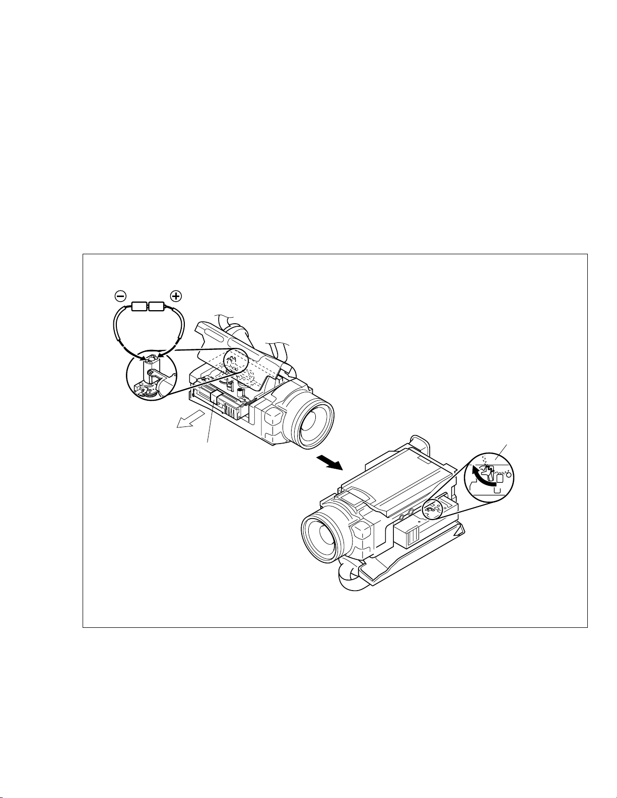
1.7 MANUAL EJECTION OF THE CASSETTE TAPE
Note:
The following procedure describes a simplified method
of ejecting the cassette tape in case it is not possible
to eject it, due to an electrical failure.
Be careful not to damage any of the parts or the tape
when performing repairs or maintenance work.
1. Remove the Power Unit (battery, DC code, etc.) from the
main unit.
2. Open the cassette cover.
3. Attach a piece of PVC tape at the front of the cassette
housing.
Note:
This helps prevent the tape from being damaged when
the Cassette Housing Assembly is moved upward at
the unloading end.
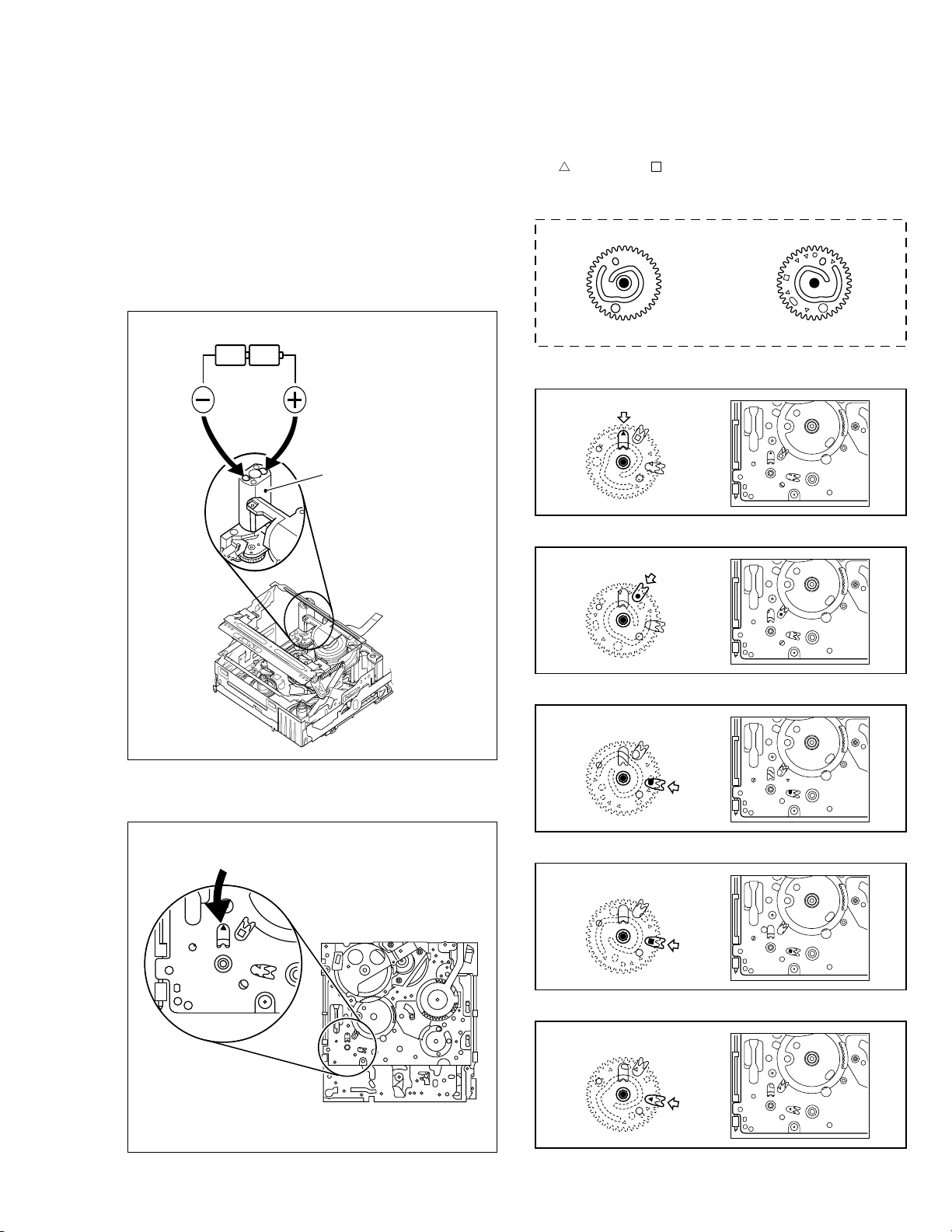
(DC3V)
4. In order to change the mechanism mode at the unloading end apply 3 V, DC to the electrode on the top surface of the Loading Motor Assembly and then set it to
the eject mode.
5. If there is any slack tape in the tape transport system,
wind it inside the cassette tape by turning the Supply
Reel Disk from the backside of the Slide Deck Assembly.
6. Peel off the PVC tape and take out the cassette tape from
the cassette housing.
Note:
Make sure that grease or a similar substance is not
attached to the surface of the tape.
Similarly, also make sure that grease or a similar sub-
stance is not attached on the Mechanism
Assembly.
PVC TAPE
REEL DISK ASSY (SUP)
Fig. 1-7-1
1-11
Page 17

1.8 EMERGENCY DISPLAY
Whenever some abnormal signal is input to the syscon
CPU, an error number (E01, as an example) is displayed
on the LCD monitor or (in the electronic view finder).
In every error status, such the message as shown below
alternately appear over and over.
• In an emergency mode, all operations except turning on/
off the POWER switch are ineffectual.
Example (in case of the error number E01):
UNIT IN
E01
SAFEGUARD MODE
E01
REMOVE AND
REATTACH BATTERY
LCD
display
E01 LOADING
E02 UNLOADING
E03 TU & SUP REEL
E04 DRUM FG
Emergency
mode
FG
Details Possible cause
In the case the encoder position is not shifted
to the next point though the loading motor has
rotated in the loading direction for 4 seconds
or more. This error is defined as [E01].
In the case the encoder position is not shifted
to the next point though the loading motor has
rotated in the unloading direction for 4 seconds or more. This error is defined as [E02].
In the case no REEL FG is produced for 4 seconds or more in the capstan rotation mode after loading was complete, the mechanism
mode is shifted to STOP with the pinch roller
set off.
This error is defined as [E03].
However, no REEL EMG is detected in the
SLOW/STILL mode.
In the case there is no DRUM FG input in the
drum rotation mode for 4 seconds or more.
This error is defined as [E04], and the mechanism mode is shifted to STOP with the pinch
roller set off.
1. The mechanism is locked during mode shift.
2. The mechanism is locked at the mechanism loading end, because the encoder position is skipped
during mechanism mode shift.
3. No power is supplied to the loading MDA.
1. The mechanism is locked during mode shift.
2. The mechanism is locked at the mechanism loading end, because the encoder position is skipped
during mechanism mode shift.
1. The idler gear does not engage with the reel disk
well.
2. Though the idler gear and reel disk are engaged with
each other, the tape is not wound because of overload to the mechanism.
3. No FG pulse is output from the reel sensor.
4. No power is supplied to the reel sensor.
5. Tape transport operation takes place with a cassette
having no tape inside.
6. The tape slackens and no pulse is produced until
the slack is taken up and the tape comes into the
normal status.
1. The drum cannot be started or drum rotation is
stopped because tape transport load is too high.
1) Tape tension is extremely high.
2) The tape is damaged or soiled with grease, etc.
2. The DRUM FG signal is not received by the syscon
CPU.
1) Disconnection in the middle of the signal line.
2) Failure of the DRUM FG pulse generator (hall element).
3. No drum control voltage is supplied to the MDA.
4. No power is supplied to the DRUM MDA.
E05 –
E06 CAPSTAN FG
1-12
– –
In the case no CAPSTAN FG is produced in
the capstan rotation mode for 2 seconds or
more. This error is defined as [E06], and the
mechanism mode is shifted to STOP with the
pinch roller set off.
However, no CAPSTAN EMG is detected in the
STILL/FF/REW mode.
1. The CAPSTAN FG signal is not received by the
syscon CPU.
1) Disconnection in the middle of the signal line.
2) Failure of the CAPSTAN FG pulse generator (MR
element).
2. No capstan control voltage is supplied to the MDA.
3. No power is supplied to the CAPSTAN MDA.
4. The capstan cannot be started or capstan rotation
is stopped because tape transport load is too high.
1) Tape tension is extremely high. (Mechanical
locking)
2) The tape is damaged or soiled with grease, etc.
(Tape tangling occurs, etc.)
Table 1-8-1
(DVC_03)
Page 18
1.9 SERVICE NOTE
1234 5
99 99 9 9 99
6 7 8 9 10 11 12 13 14 15 16 17 18
1
Fig. 1-3-1
Fig. 1-3-2a
Fig. 1-3-2cFig. 1-3-2b
Symbol No.
Removing order of screw
Place to stick screw
Reference drawing
Screw tightening torque
→
→
→
→
Symbol No.
Removing order of screw
Place to stick screw
Reference drawing
Screw tightening torque
→
→
→
→
→
Symbol No.
Removing order of screw
Place to stick screw
Reference drawing
Screw tightening torque
→
→
→
→
→
Removing order of screw
Place to stick screw
Reference drawing
Screw tightening torque
→
→
→
→
12
34 567
MONITOR ASSY
II
7
OP BLOCK ASSY
Fig. 1-5-1
VIV IVIV
12
34
5678
9
10
11 12
< NOTE >
1)
9
;
Don't reuse the screw, because screw lock bond was applied to them.
2) Pay careful attention to tightening torque for each screw.
I
: 0.069N·m (0.7kgf
·cm)
II : 0.078N
·m (0.8kgf·cm)
III : 0.059N
·m (0.6kgf·cm)
IV
: 0.118N·m (1.2kgf
·cm)
V : 0.147N
·m (1.5kgf·cm)
Fig. 1-6-1
→
I
9999
99
III
19 20 21 22 23
99 9 99
24 25 26 27 28 29 30 31 32 33 34 35
3
5
2
64
Fig. 1-3-3
Fig. 1-3-6Fig. 1-3-4 Fig. 1-3-5
IIII
36 37 38 39 40
99
41 42 43 44 45 46 47 48 49 50 51
7
980
@
Fig. 1-3-7
Fig. 1-3-8 Fig. 1-3-9
Fig. 1-3-10
Symbol No.
Removing order of screw
Place to stick screw
Reference drawing
Screw tightening torque
→
→
→
→
→
IIII II
6
Fig. 1-4-1
VF UNIT
III II
12
3
45
6
7
8
9
10
11
12
Table 1-9-1
1-13
Page 19

1-14
Page 20
SECTION 2
MECHANISM ADJUSTMENT
2.1 PRELIMINARY REMARKS ON ADJUSTMENT AND REPAIR
2.1.1 Precautions
1. When fastening parts, pay careful attention to the tight-
ening torque of each screw. Unless otherwise specified,
tighten a screw with the torque of 0.039 N
2. Be sure to disconnect the set from the power supply be-
fore fastening and soldering parts.
3. When disconnecting/connecting wires, be careful not to
get them and their connectors damaged. (Refer to the
Section 1.)
4. When replacing parts, be very careful neither to dam-
age other parts nor to fit wrong parts by mistake.
2.1.2 Notes on procedure for disassemby/assembly
The disassembling procedure table (Table 2-4-1 on page
2-5,a part of the table is shown below for reference)shows
the procedure to disassemble/reassemble mechanism
parts.
Carefully read the following explanation before starting actual disassembling/reassembling work. The item numbers
(circled numbers)in the following explanation correspond
to those appearing under respective columns of the table.
(1) Circled numbers appearing in this column indicate the
order to remove parts. When reassembling, follow these
numbers in the reverse order. Circled numbers in this
column correspond to those appearing in drawings of
this section.
(2) This column shows part names corresponding to circled
numbers in the left column.
(3) The symbol (T or B)appearing in this column shows the
side which the objective part is mounted on.
T =the upper side, B =the lower side
(4) Symbols appearing in this column indicate drawing
numbers.
Step Part Name Fig. Point Note Remarks
•
m (0.4 kgf•cm).
(5) This column indicates parts and points such as screws,
washers,springs,and others to be removed/fitted for disassembling/reassembling the mechanism. Besides such
the parts, this column occasionally indicates working
points.
P = Spring
W = Washer
S = Screw
* = Lock (L),soldering (SD),shield,connector (CN),
etc.
Example • Remove ((W1)=Washer W1.
• **Remove the solder at (SD1)=Point SD1.
• **Disconnect
(6) Numbers in this column represent the numbers of notes
in the text.For example, “1” means “Note 1”.
(For parts that need phase adjustment after reassembling, refer to “2.6 MECHANISM ADJUSTMENTS”.)
(7) This column indicates required after-disassembling/-re-
assembling work such as phase adjustment or mechanism adjustment.
=Connector Å .
Å
NO. PART NAME FIG. POINT NOTE REMARKS
1 CASSETTE HOUSING ASSY T Fig.2-4-3 3(S1),(L1a)-(L1e)
2 UPPER BASE ASSY T Fig.2-4-4 (S2),(L2a),(L2b)
3 DRUM ASSY T (S3a),2(S3b)
4 REEL DISK ASSY(SUP) T Fig.2-4-5 (W4)
5 REEL DISK ASSY(TU) T (W5)
6 REEL COVER ASSY T 2(W6),(S6a),2(S6b)
(1) (2) (3) (4) (5) (6) (7)
NOTE1a,b,c,d
NOTE
2
NOTE3a,b
NOTE4a
NOTE
5
NOTE
6
ADJUSTMENT
ADJUSTMENT
2-1
Page 21
2.2 JIGS AND TOOLS REQUIRED FOR DISASSEMBLY, ASSEMBLY AND ADJUSTMENT
2.2.1 Tools required for adjustments
1
3
5
7
9
11
13
15
Torque Driver
YTU94088
Tweezers
P-895
Guide Driver (Hexagonal)
D-770-1.27
Slit Washer Installation Jig
YTU94121A
Jig Connector cable
YTU93106B
Communication cable
YTU93107A
Alignment Tape
MC-2
Cassette Torque Meter
YTU94151A
2
Chip IC Replacement Jig
4
6
Slit Washer Installation Jig
8
10
12
Service Support System
14
16
Bit
YTU94088-003
PTS40844-2
Adjustment Driver
YTU94028
YTU94121B
Extension connector
YTU94145C-30
PC cable
QAM0099-002
YTU94057-50
Cleaning Cloth
KSMM-01
1. Torque Driver
Be sure to use to fastening the mechanism and exterior
parts because those parts must strictly be controlled for
tightening torque.
2. Bit
This bit is slightly longer than those set in conventional
torque drivers.
3. Tweezers
To be used for removing and installing parts and wires.
4. Chip IC Replacement Jig
To be used for adjustment of the camera system.
5. Guide Driver (Hexagonal)
To be used to turn the guide roller to adjustment of the
linarity of playback envelope.
6. Adjustment Driver
To be used for adjustment.
7. Slit Washer Installation Jig
To be used to install slit washers.
8. Slit Washer Installation Jig (NEW TYPE)
To be used to install slit washers.
9. Jig Connector Cable
Connected to CN107 of the main board and used for
electrical adjustment, etc.
10. Extension Connector
Connect this extension connector to the connector of the
jig connector cable for extending the cable connector.
For supplying the power through the coupler by re-
Note:
moving the cover (for jig), use this extension connector double for connecting the jig connector cable.
11. Communication Cable
Connect the Communication cable between the PC cable and Jig connector cable when performing a PC adjustment.
12. PC Cable
To be used to connect the VideoMovie and a personal
computer with each other when a personal computer is
used for adjustment.
13. Alignment Tape
To be used for check and adjustment of interchangeability of the mechanism.
14. Service Support System
To be used for adjustment with a personal computer.
15. Cassette Torque Meter
This is used to cheek the back tension and play torque
during mechanism adjustment.
When using the cassette torque meter, install the
Note:
service support system software in advance.
•
LED : Forced to ON
•
EJECT SW : OFF (Cancel)
The above setting is required to prevent any tape
damage that may occur because the cassette
torque meter cannot detect the leading/trailing sections of the tape.
16. Cleaning Cloth
Recommended cleaning cloth to wipe down the video
heads, mechanism (tape transport system), optical lens
surface.
2-2
Table 2-2-1
Page 22
2.3 DISASSEMBLY/ASSEMBLY OF MECHANISM AS-
<SUB CAM GEAR>
TOP VIEW BOTTOM VIEW
<C IN mode>
<SHORT FWD mode>
<STOP mode>
<REV mode>
<PLAY mode>
SEMBLY
2.3.1 General statement
The mechanism should generally be disassembled/assembled in the C.IN mode (ASSEMBLY mode). (Refer to Fig.
2-3-1,2.)
However, when the mechanism is removed from the main
body, it is set in the STOP mode. Therefore, after the
mechanism is removed from the main body, supply 3 V DC
to the electrode on the top of the loading motor to enter
the mechanism mode into the C,IN mode compulsory.
<Mechanism assembly/Cassette housing assembly>
DC3V
2.3.2 Explanation of mechanism mode
The mechanism mode of this model is classified into five
modes as shown in Table 2-3-1. Each mechanism mode
can be distinguished from others by the relative position
”, “Q”, “Q” “ ” marks on the sub cam gear to the in-
of “
ner or outer protrusion on the main deck.
Refer to Fig. 2-3-3 to 2-3-8 below.
Fig. 2-3-3
<Back side of the mechanism assembly>
C IN mode
LOADING MOTOR
Fig. 2-3-4
Fig. 2-3-5
Fig. 2-3-1
Fig. 2-3-6
Back side of deck
Fig. 2-3-2
Fig. 2-3-7
Fig. 2-3-8
2-3
Page 23
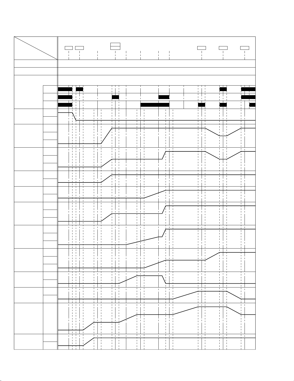
2.3.3 Mechanism timing chart
PARTS
MAIN CAM
SUB CAM
ROTARY
ENCODER
EJECT LEVER
TENSION ARM
TU ARM
SLIDE DECK
BRAKE (S)
BRAKE (T)
MODE
ON
OFF
L. END
LOCK
L. END
OFFPAD ARM
ON
OFF
LOAD
L. END
LOADSUP. L. ARM
L. END
LOADTU. L. ARM
PRESS
LOADP. ROLLER
ON
OFF
ON
OFF
SHORT
EJECT
CAS. IN
-12.40° (22.44°) (69.53°) (80.5°) (150.58°) (153.5°)58.71°0° 177.79° 212.77° 243.94°
-16.97° (30.71°) (95.14°) (110.06°) (206.06°) (210.05°)80.34°0° 243.29° 291.16° 333.82°
-15° (27.14°) (84.08°) (97.35°) (182.10°) (185.63°)71°0°
-13°-3° 3° 68°
a
b
c
UL
UL
UL
UL
UL
UL
R
RELEASE
TU. P. B
START
SLIDE SLIDE
START
TU. P. B
END END
STOP PLAYREVFWD
215°
212° 218°
257.3°
254.3° 260.3°
295°
292° 310°74°
CTL PLATE
RELEASE
LEVER
2-4
C
L
ON
OFF
Table 2-3-1
Page 24

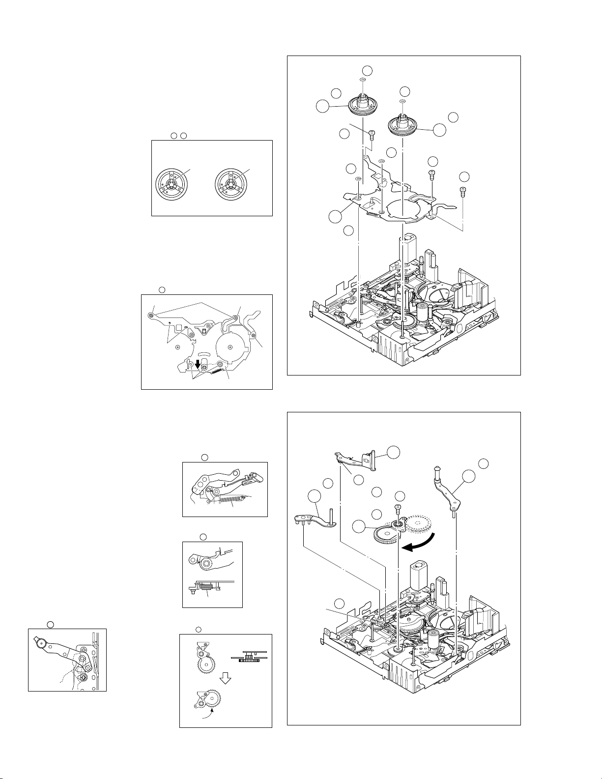
2.4 DISASSEMBLING PROCEDURE TABLE
NO. PART NAME FIG. POINT NOTE REMARKS
1 CASSETTE HOUSING ASSY T Fig.2-4-3 3(S1),(L1a)-(L1e)
2 UPPER BASE ASSY T Fig.2-4-4 (S2),(L2a),(L2b)
3 DRUM ASSY T (S3a),2(S3b)
4 REEL DISK ASSY(SUP) T Fig.2-4-5 (W4)
5 REEL DISK ASSY(TU) T (W5)
6 REEL COVER ASSY T 2(W6),(S6a),2(S6b)
7 TENSION ARM ASSY T Fig.2-4-6 —
8 SLANT POLE ARM ASSY T —
9 TU ARM ASSY T —
10 SWING ARM ASSY T (S0)
11 SLIDE DECK ASSY T Fig.2-4-7a (W
12 PAD ARM ASSY T Fig.2-4-7b (P@),(L@),(W@)
13 SUP BRAKE ASSY T (P#),(L#),(S#)
14 TU BRAKE ASSY T (P$),(L$),(W$)
15 TENSION CTL LEVER ASSY T Fig.2-4-8 —
16 CENTER GEAR T —
17 PINCH ROLLER ARM F. ASSY T (W&)
18 TENSION CTL PLATE ASSY T —
19 BRAKE CTL LEVER ASSY T —
20 MOTOR BRACKET ASSY T Fig.2-4-9 3(S)),(L)a),2(L)b)
21 GUIDE RAIL ASSY T
22 SLIDE LEVER 2 ASSY T —
23 LOADING PLATE ASSY T (W‹)
24 MODE GEAR T —
25 EJECT LEVER T (Wfi)
26 BASE R ASSY T Fig.2-4-10 (Sfla),(Sflb),2(Lfl)
27 ROTARY ENCODER T 2(S‡)
28 GEAR COVER ASSY T (S°a),2(S°b)
29 MAIN CAM ASSY T —
30 SLIDE ARM ASSY T Fig.2-4-11 —
31 CONNECT GEAR 2 T —
32 SUB CAM ASSY T (S™)
33 CONTROL ARM ASSY T —
34 REEL GEAR 1 T —
35 / 36
36 CAPSTAN MOTOR T (S§)
37 MAIN DECK ASSY T —
DRUM BASE ASSY/ T Fig.2-4-12 3(S∞)
CAPSTAN MOTOR
),2(S!a),(S!b),
!
2(L!a),2(L!b),(L!c)
2(W⁄),(S⁄),2(L⁄a),(L⁄b)
NOTE1a,b,c,d
NOTE
2
NOTE3a,b
NOTE
4
NOTE
5
NOTE
6
NOTE
7
NOTE
8
NOTE
9
NOTE
0
NOTE!a,b
NOTE
@
NOTE
#
NOTE
$
NOTE
%
NOTE
^
NOTE
&
NOTE
*
NOTE
(
NOTE
)
NOTE
⁄
NOTE
¤
NOTE
‹
NOTE
›
NOTE
fi
NOTE
fl
NOTE
‡
—
NOTE
·
NOTE
‚
NOTE
¡
NOTE
™
NOTE
£
NOTE
¢
NOTE∞a,b
NOTE
§
—
ADJUSTMENT
ADJUSTMENT
ADJUSTMENT / 夝
ADJUSTMENT
ADJUSTMENT
ADJUSTMENT
ADJUSTMENT / 夝
ADJUSTMENT / 夝
ADJUSTMENT
ADJUSTMENT
ADJUSTMENT
ADJUSTMENT
ADJUSTMENT
ADJUSTMENT
ADJUSTMENT
ADJUSTMENT / 夝
ADJUSTMENT
ADJUSTMENT
ADJUSTMENT
PHASE ADJUSTMENT
PHASE ADJUSTMENT
ADJUSTMENT
PHASE ADJUSTMENT
ADJUSTMENT
ADJUSTMENT
ADJUSTMENT
MARK: 夝 After assembly, perform adjustments.
Table 2-4-1
2-5
Page 25
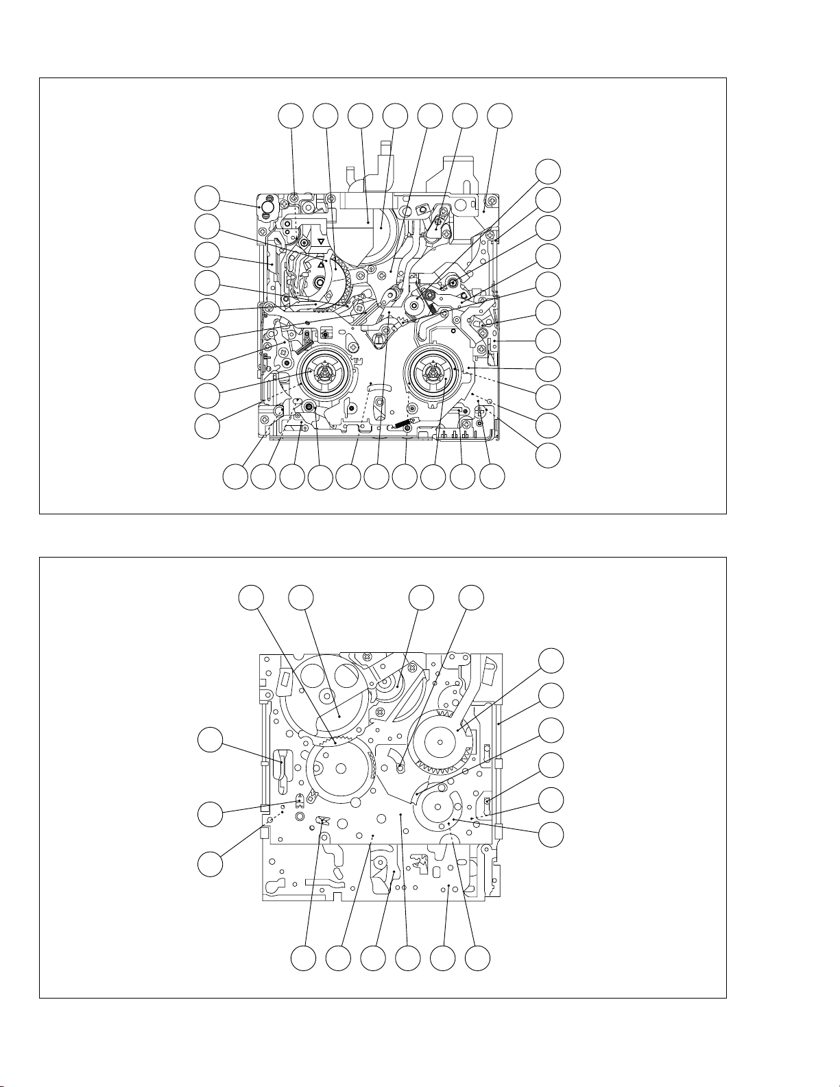
< TOP VIEW >
24 27 2 3 36 3521
17
< BOTTOM VIEW >
20
23
18
8
7
22
12
4
29
19
34
143128161530
13
Fig. 2-4-1
5
36 3 22
26
34
9
10
33
26
6
37
25
32
11
26
32
25
31 16 6
Fig. 2-4-2
37
11
27
20
30
18
19
29
30
2-6
Page 26
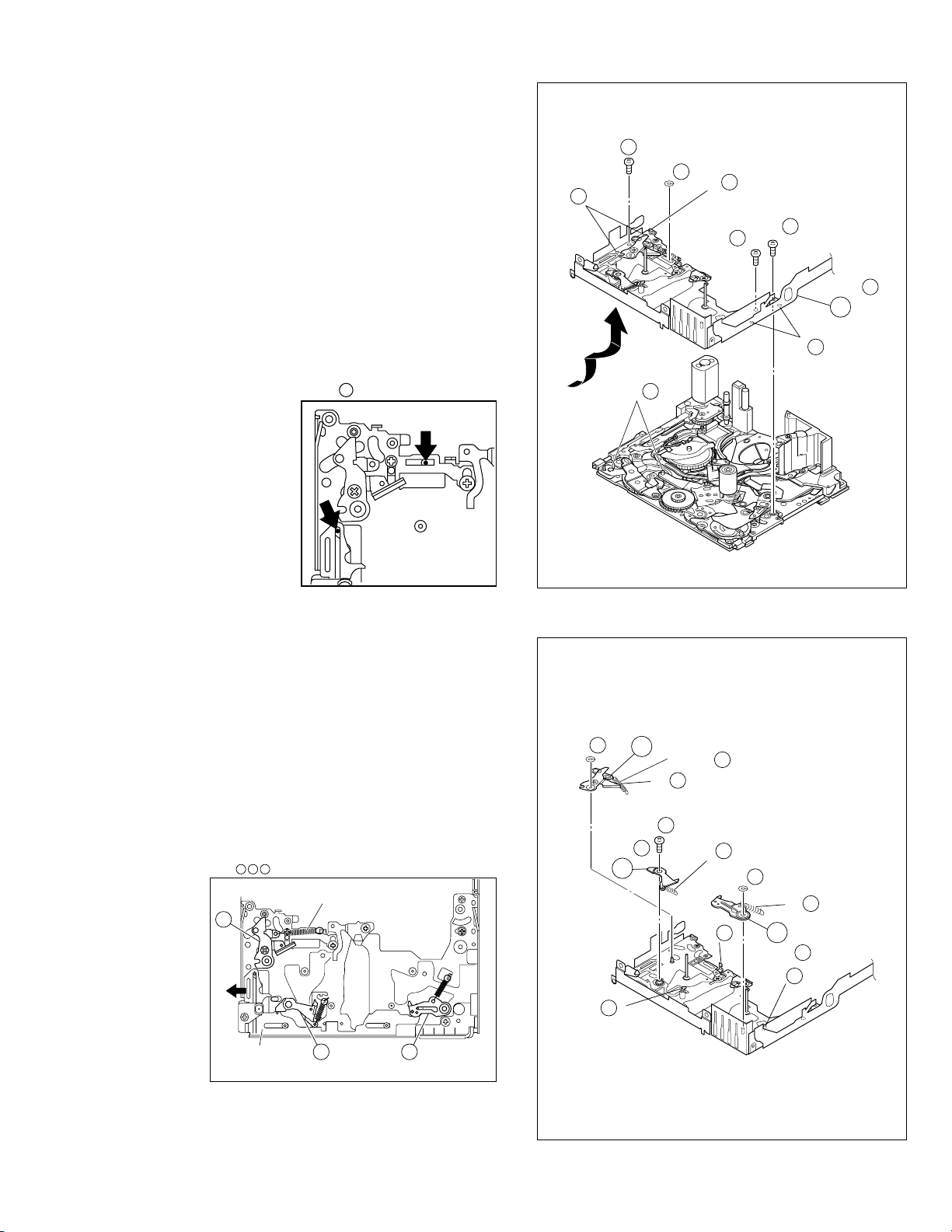
2.4.1 Disassembly/assembly
1
(S )
1
2
(S )
1
1
NOTE d
1
NOTE c
1
NOTE b
1
NOTE a
1
(S )
1
3
(L d)
LOCK
LEVER
1
(L a)
1
(L e)
1
(L c)
1
(L b)
1
NOTE d
1
2
3
(S )
2
4
(S b)
7
3
(S b)
6
3
(S a)
5
3
(L b)
2
(L a)
2
NOTE
2
NOTE
3
NOTE b
3
NOTE
2
a
CASSETTE HOUSING ASSY
1.
1
NOTE1a:
Be careful not to damage any of the
parts during work.
NOTE1b:
Special care is required in mounting.
1
NOTE b
NOTE1c:
NOTE c
When mounting, the CASSETTE
HOUSING ASSY should be attached in the Eject status. Pay
heed to the positions of the LOCK
LEVER and EJECT LEVER during
mounting.
NOTE1d:
When mounting, be sure to locate the
FPC in the gap.
2.
UPPER BASE ASSY
2
DRUM ASSY
3
NOTE
NOTE2:
When mounting, be sure to insert
the FPC reinforcing sheet.
1
EJECT
LEVER
NOTE d
2
LOCK
LEVER
1
Fig. 2-4-3
NOTE3a:
Be mindful of scratches or damage
during work.
NOTE3b:
Be careful not to attach screws incorrectly.
3
NOTE
b
5
7
6
Fig. 2-4-4
2-7
Page 27
REEL DISK ASSY(SUP)
3.
4
REEL DISK ASSY(TU)
5
REEL COVER ASSY
6
NOTE4:
Be careful not to attach the REEL DISK wrongly. The Supply side can be identified by the white color at the center.
4 5
NOTE5:
Be careful not to attach the
REEL DISK wrongly. The
NOTE ,
REEL DISK ASSY
WHITE
BLACK
Take-up side can be identified by the black color at
the center.
SUP
TU
NOTE6:
Perform the following steps for mounting.
1. Move the RELEASE GUIDE back and align the 2 holes
with the pins.
2. Attach the PINCH ROLLER ARM ASSY by aligning the
positions.
3. Attach the SUB DECK
ASSY by aligning the
positions.
NOTE
6
3
5
2
4. Check that the parts
below them are located in the correct
positions.
4
5. Tighten the 2 screws.
6. Tighten the screw.
7. Attach the 2 SLIT
WASHER parts.
1, 7
RELEASE GUIDE
4
(W )
5
NOTE
4
(W )
4
8
6
5
(S b)
5
10
6
9
6
(S a)
6
(W )
6
(W )
NOTE
(S a)
6
NOTE
6
6
Fig. 2-4-5
4.
TENSION ARM ASSY
7
SLANT POLE ARM ASSY
8
TU ARM ASSY
9
SWING ARM ASSY
0
NOTE7:
When detaching, remove the spring
of the @ PAD ARM ASSY in advance.
Pay attention to the attachment position.
NOTE8:
Be careful not to lose any parts
(such as a spring).
NOTE9:
Pay attention to the
mounting position.
9
NOTE
7
NOTE
SPRING
8
NOTE
SPRING
10
NOTE
TOP SIDE
NOTE
7
NOTE
7
(P )
NOTE
NOTE
7
10
8
NOTE
8
8
10
11
10
(S )
9
9
NOTE0:
When detaching, remove the
screw then remove the SWING
ARM ASSY by pulling it up and
turning it.
2-8
Fig. 2-4-6
Page 28
5.
(W )
11
11
(S b)
14
11
(S a)
12
11
(S a)
13
11
(L b)
11
(L a)
11
(L c)
11
NOTE a
11
NOTE b
11
SLIDE DECK ASSY
!
NOTE!a:
Each of the parts on the SLIDE DECK ASSY can be replaced separately.
When detaching the assembly, if there is no need to replace
any of its parts, remove the SLIDE DECK ASSY as it is.
NOTE!b:
When mounting, pay attention to the positions of the
¤
SLIDE LEVER (2) studs to which the SLIT WASHERS are
attached and the BRAKE CONTROL LEVER ASSY.
When mounting, position the CONTROL PLATE on the left
side.
Pay attention to the position of the SLIDE GUIDE PLATE
during mounting.
11
NOTE
b
6.
PAD ARM ASSY
@
SUP BRAKE ASSY
#
TU BRAKE ASSY
$
NOTE@:
The spring may have already been disengaged when the
8
SLANT POLE ARM ASSY was removed.
NOTES#/$:
When mounting, pay attention to the correct positioning.
Mount the CONTROL PLATE by moving it fully toward the
left side.
12 13 14
NOTE
12
SPRING
CONTROL
PLATE
13 14
12
(W )
NOTE
(L )
13
13
12
(P )
15
(S )
13
NOTE
12
13
Fig. 2-4-7a
12
13
(P )
(W )
12
(L )
14
14
NOTE
(L )
14
(P )
14
14
Fig. 2-4-7b
2-9
Page 29
TENSION CTL LEVER ASSY
7.
%
CENTER GEAR
^
PINCH ROLLER ARM F. ASSY
&
TENSION CTL PLATE ASSY
*
BRAKE CTL LEVER ASSY
(
NOTES%/^:
When mounting, pay attention to the correct positioning.
15
NOTE
NOTE
16
(TOP)
(BOTTOM)
NOTES*/(:
When mounting, pay at-
NOTE&:
Take care against grease
attachment during work.
17
NOTE
tention to the correct positioning.
19
NOTE
18
NOTE
NOTE
15
NOTE
19
15
19
NOTE
18
18
NOTE
17
16
17
NOTE
17
(W )
16
MOTOR BRACKET ASSY
8.
)
GUIDE RAIL ASSY
⁄
SLIDE LEVER 2 ASSY
¤
LOADING PLATE ASSY
‹
MODE GEAR
›
EJECT LEVER
fi
NOTE):
When mounting, pay attention to the positioning of the sliding parts.
21
NOTE
NOTE⁄:
When mounting, take care
that no part is allowed to
float or rattle.
NOTES¤/‹/›/fi:
NOTE
When mounting, pay attention to the
correct positioning.
23
NOTE
22
NOTE
NOTE
24
Fig. 2-4-8
20
21
21
21
NOTE
(W )
(W )
23
22
21
NOTE
19
21
(S )
22
(L a)
21
(L b)
21
NOTE
18
20
(S )
20
20
17
20
(S )
NOTE
16
20
(S )
23
23
(L b)
25
(W )
(L a)
20
(W )
20
NOTE
24
24
25
25
NOTE
2-10
NOTE
25
Fig. 2-4-9
Page 30
BASE R ASSY
9.
fl
ROTARY ENCODER
‡
GEAR COVER ASSY
°
MAIN CAM ASSY
·
NOTEfl:
When mounting, fold the sliding
part to the inner side.
NOTE
22
27
(S )
27
NOTE
26
27
23
27
(S )
25
26
28
24
28
(S a)
20
26
(S b)
28
(S b)
(S b)
NOTE‡:
When mounting, pay attention to
the correct positioning and the
FPC layout.
NOTE
·
:
When mounting, pay attention to
the correct positioning.
SLIDE ARM ASSY
10.
‚
CONNECT GEAR 2
¡
SUB CAM ASSY
™
CONTROL ARM ASSY
£
REEL GEAR 1
¢
NOTE
‚
:
When mounting, pay attention to the
correct positioning and the FPC layout.
NOTE
NOTE
NOTE
21
26
27
(S a)
28
29
29
NOTE
29
26
NOTE
26
26
(L )
Fig. 2-4-10
30
30
NOTE
30
27
32
(S )
NOTE
32
32
NOTE
34
34
NOTE¡:
When mounting, pay attention to the position of the front and back.
NOTE
(BOTTOM)
31
(TOP)
NOTES™/£/¢:
When mounting, pay attention to the correct positioning and
the FPC layout.
34
32 33
NOTE /
32
33
NOTE
NOTE
31
31
Fig. 2-4-11
33
NOTE
33
2-11
Page 31

11.
DRUM BASE ASSY
∞
CAPSTAN MOTOR
§
MAIN DECK ASSY
¶
NOTES
∞
a /§:
When detaching, remove them together and then separate
from ∞a.
§
∞
b:
NOTE
When mounting, attach the DRUM BASE ASSY so that the
screw hole is located at the center of the ellipse.
35
NOTE b
35
28
35
(S )
29
35
(S )
31
36
(S )
30
35
(S )
NG
OK
NG
NOTE
36
36
Fig. 2-4-12
37
NOTE
35
a
2-12
(Z27 Ver.1)
Page 32

2.4.2 List of procedures for disassembly
(W )
13
(P )
18
(S )
20
13
13
12
(W )
14
(S )
20
17
12
20
(S b)
8
(P )
14
(W )
14
(P )
14
11
8
2
(S )
12
(P )
16
(S )
1
(W )
4
(S a)
(W )
6
7
(W )
22
(S )
20
18
27
1
4
29
(S )
35
5
3
(S )
35
36
17
2
2
(S )
17
(W )
31
3
35
30
35
(S )
1
1
4
5
(W )
9
6
6
(W )
6
5
8
6
(S a)
(S b)
(S )
9
6
9
21
19
21
28
(S )
35
7
3
(S b)
(S a)
6
3
(S b)
23
27
30
23
(S )
11
10
(S )
(S a)
(S )
23
27
13
11
3
1
34
10
12
11
(S a)
11
21
(W )
22
(W )
(S )
21
25
28
(S b)
15
29
16
31
26
28
(S b)
28
24
28
(S a)
19
24
37
Fig. 2-4-13
20
26
(S a)
26
25
(W )
(S )
25
27
32
32
33
2-13
Page 33

2.5 CHECKUP AND ADJUSTMENT OF MECHANISM PHASE
MODE GEAR
24
Align the MODE GEAR with the Main Deck
Assembly hole.
Note:
The MODE GEAR may
be displaced during the
mechanism operation,
however it can be
checked from the rear
and realigned during
manual assembly.
27
ROTARY ENCODER
Mount the ROTARY ENCODER by aligning its mark ( )
and the mark ( ) of the Main Deck Assembly.
Note:
Be careful when handling the FPC during mounting.
34
REEL GEAR 1
Align the REEL GEAR 1 with
the Main Deck Assembly hole.
Note:
The REEL GEAR 1 may be
displaced during mechanism
operation, however this can
be checked from the rear and
realigned during manual
assembly.
MAIN CAM ASSY/ 30 SLIDE ARM ASSY
29 32
When mounting the SLIDE ARM ASSY align it with the
Main Deck Assembly and MAIN CAM ASSY holes.
Note:
During the mounting procedure, make sure that the 32 .
SUB CAM ASSY is in the correct mounting position.
Fig. 2-5-1
SUB CAM ASSY/ 33 CONTROL ARM ASSY
Mount the SUB CAM ASSY hole to align with the CONTROL
ARM ASSY and Main Deck Assembly holes and then tighten
them all together with a screw.
The screw tightening torque should be 0.039 N•m (0.4 kgf•cm)
Note:
When mounting it, make sure that the 29 MAIN CAM ASSY is
in the correct mounting position.
2-14
Page 34

2.6 MECHANISM ADJUSTMENTS
2.6.1 Adjustment of the slide guide plate
Use Fig. 2-6-1 as the reference unless otherwise specified.
1. Set the PLAY mode.
See Fig. 2-3-8.
2. Loosen the screws A , B ).
3. With the Main Deck Assembly and Slide Deck Assembly pushed inside the unit, tighten the screws ( A , B )
while applying pressure on the slit washers of the slide
guide plate.
The pressure applied should be enough to enable utilization of the rebounding force of the springs.
The tightening torque should be 0.069 N
•
m (0.7 kgf•cm).
4. Check the operation.
Repeat unloading and loading several times and make
sure that these operations can be performed smoothly
without producing rattles.
3
2, 3
SCREW
3
3
3
A
2,3
SCREW
B
3
Fig. 2-6-1
2-15
Page 35

2.6.2 Adjustment of the Tension Arm and Pad Arm Assemblies
Use Fig. 2-6-2 as the reference unless otherwise specified.
1. Set the PLAY mode.
Se Fig. 2-3-8.
2. Loosen the screw A .
3. With the take-up side at the bottom, align the extreme
end of the Tension Arm Assembly with the crossed
grooves on the screw B that retains the Loading Motor
Assembly and then tighten the screw A .
The tightening torque should be 0.069 N
•
m (0.7 kgf•cm).
4. Check the operation.
Repeat unloading and loading several times and make
sure that the Tension Arm Assembly is located within the
normal range.
Note :
With the above checking method, a Torque Meter is not used.
When a Torque meter is used, the following are
the reference values:
2, 3
SCREW
SCREW
A
TENSIOM
ARM ASSY
B
Back Tension : 2.0 to 6.0 g•cm
Play Torque : 8.3 to 12.5 g
•
cm
2.6.3 Adjustment of the Slide Lever 2
Use Fig. 2-6-3 as the reference unless otherwise specified.
1. Set the C IN mode.
See Fig. 2-3-4.
2. Loosen the screw A .
3. Set the Main Deck and Slide Deck Assemblies apart so
that they do not rattle, then tighten the screw A by
screwing it fully toward the Drum Assembly.
The tightening torque should be 0.069 N
•
m (0.7 kgf•cm).
4. Check the operation.
Repeat unloading and loading several times and make
sure that these operations can be performed smoothly
without producing rattles.
2, 3
SCREW
Fig. 2-6-2
3
A
2-16
3
Fig. 2-6-3
Page 36

2.7 JIG CONNECTOR CABLE CONNECTION
Remove one screw (1) first and the cover (JIG) next.
GUIDE ROLLER (TU) ASSY
GUIDE ROLLER (SUP)
ASSY
COMMINICATION CABLE JIG CONNECTOR
to 8 pin
RED
( JLIP_RX )
to 9 pin
( JLIP_TX )
WHITE
to 5 or 23 pin
BLACK
( GND )
JIG CONNECTOR CABLE
COMMUNICATION CABLE
MAIN BOARD ASSY CN107
16
1
17
2
D_REG3V
DJIG.MOD
DJIG_SCL
DJIG.SPT
18
3
19
4
20
5
21
6
MONI_CHG(REC_I)
22
7
CHG_STOP
23
8
24
9
JLIP_RX
PB_CLK
JLIP_TX
25
10
26
ENV_OUT
11
27
12
28
13
PB_VCO
MAIN_VCO
VPPC_5V
AL_3VSYS
29
14
30
15
CJIG_MOD
CJIG_SCK
CJIG_SPT
TDO_F
TDI_F
TCMK
TMS
TRST
GND
SBE
SPA
GND
GND
HID1
ATFI
FS_PLL
COVER
(JIG)
1
Fig. 2-7-1
EXTENSION CONNECTOR
For supplying the power through the coupler by
NOTE:
removing the cover (for jig), use this extension
connector double for connecting the jig connector
cable.
TO PC CABLE
JIG CONNECTOR CABLE
1
2
3
4
5
6
7
8
9
10
11
12
13
14
15
16
17
18
19
20
21
22
23
24
25
26
27
28
29
30
NC
NC
NC
NC
GND
NC
NC
JLIP_RX
JLIP_TX
HID1
NC
MAIN_VCO
NC
NC
NC
NC
NC
NC
NC
NC
NC
MOIN_CHG(REC_I)
GND
NC
NC
ENV_OUT
NC
NC
FS_LL
NC
CN107
Fig. 2-7-2
2-17
Page 37

2.8 SERVICE NOTE
Use the following chart to manage mechanism parts that are removed for disassembling the mechanism.
Fig.
1
CASSETTE HOUSING ASSY UPPER BASE ASSY
Fig.
2
2
I
4
I
3
Fig. Fig.
3
DRUM ASSY
2
I
4
I
4
2
I
4
I
5
REEL DISK ASSY(SUP)
4
REEL DISK ASSY(TU)
5
2
I
4
I
4
REEL COVER ASSY
6
Fig.
TENSION ARM ASSY
7
SLANT POLE ARM ASSY SWING ARM ASSYTU ARM ASSY
8 9
2
I
4
I
6
Fig. Fig.
2
I
4
I
7
a
SLIDE DECK ASSY
11
2
I
4
I
7
b
PAD ARM
ASSY
1312
10
SUP
BRAKE
ASSY
14
TU BRAKE
ASSY
2-18
Table 2-8-1a
Page 38

Fig.
2
I
4
I
8
TENSION CTL
15
LEVER ASSY
CENTER GEAR
16
PINCH ROLLER
17
ARM F. ASSY
TENSION
18
CTL PLATE
ASSY
BRAKE CTL
19
LEVER
ASSY
Fig.
2
I
4
I
9
Fig.
2
I
4
I
10
Fig.
MOTOR
20
BRACKET
ASSY
BASE R ASSY ROTARY
26
SLIDE ARM
30
ASSY
31
27
CONNECT
GEAR 2
GUIDE
21
RAIL ASSY
ENCODER
32
28
SUB CAM
ASSY
SLIDE LEVER 2
22
ASSY
MODE GEAR EJECT LEVER
24
GEAR COVER
ASSY
33
CONTROL
ARM ASSY
23
25
MAIN CAM ASSY
29
34
LOADING
PLATE ASSY
REEL GEAR 1
2
I
4
I
11
Fig.
2
I
4
I
12
DRUM BASE ASSY
35
CAPSTAN MOTOR MAIN DECK ASSY
36
Table 2-8-1b
37
2-19
Page 39

SECTION 3
ELECTRICAL ADJUSTMENT
3.1 PRECAUTION
1. Precaution
Both the camera and deck sections of this model needs a
personal computer for adjustment except simple adjustment
with potentiometers. If some of the following parts is replaced
for repair or other reason, the repaired set must be adjusted
with a personal computer.
• OP block
2
• E
PROM (IC1003 of MAIN board)
• MONITOR
2
• E
PROM (IC7302 of MONITOR board)
In the event of malfunction with electrical circuits, troubleshooting with the aid of proper test instruments most be done
first, and then commence necessary repair, replacement and
adjustment, etc.
1. In case of wiring to chip test points for measurement,
use IC clips, etc. to avoid any stress.
2. Since connectors are fragile, carefully handle them in disconnecting and connecting.
3. Shortcircuit between operation un it and DECK chassis.
Jig Connector Cable
5
Communication Cable
7
9
Alignment Tape
YTU93106B
YTU93107A
MC-2
Extension connector
6
8
10
YTU94145C-30
PC Cable
QAM0099-002
Service Support System
YTU94057-50
2. Required test equipment
1. Color TV monitor.
2. AC power adapter/charger
3. Oscilloscope (dual-trace type, observable 100 MHz or
higher frequency)
Note :
It is recommended to use one observable 300 MHz
or higher frequency.
4. Digital voltmeter
5. Frequency counter (with threshold level adjuster)
6. Personal computer
3. Tools required for adjustments
1
3
Torque Driver
YTU94088
Tweezers
P-895
2
Chip IC Replacement Jig
4
Bit
YTU94088-003
PTS40844-2
INF Adjustment Lens
11
13
15
17
YTU92001B
Camera Stand
YTU93079
Gray Scale Chart
YTU94133A
B to B connector Assy
YTU94153A-120
INF Adjustment Lens Holder
12
14
16
YTU94087
Light box Assembly
YTU93096A
Color Bar Chart
YTU94133C
3-1
Table 3-1-1a
Table 3-1-1b
Page 40

1. Torque driver
Be sure to use to fastening the mechanism and exterior parts because those parts must strictly be controlled for tightening torque.
2. Bit
This bit is slightly longer than those set in conventional
torque drivers.
3. Tweezers
To be used for removing and installing parts and wires.
4. Chip IC replacement jig
To be used for adjustment of the camera system.
5. Jig connector cable
Connected to CN107 of the main board and used for
electrical adjustment, etc.
6. Extension connector
Connect this extension connector to the connector of
the jig connector cable for extending the cable connector.
Note :
For supplying the power through the coupler by
removing the cover (for jig), use this
extension connector double for connecting the
jig connector cable.
7. Communication Cable
Connect the Communication cable between the PC
cable and Jig connector cable when performing a PC
adjustment.
8. PC cable
To be used to connect the VideoMovie and a personal
computer with each other when a personal computer
is used for adjustment.
9. Alignment tape
To be used for check and adjustment of interchangeability of the mechanism.
10. Service support system
To be used for adjustment with a personal computer.
11. INF adjustment lens
To be used for adjustment of the camera system.
12. INF adjustment lens holder
To be used together with the camera stand for operating the VideoMovie in the stripped-down
condition such as the status without the exterior parts
or for using commodities that are not yet conformable
to the interchangeable ring.
13. Camera stand
To be used together with the INF adjustment lens
holder.
14. Light box assembly
To be used for adjustment of the camera system.
15. Gray scale chart (for Light box assembly)
To be used for adjustment of the camera system.
16. Color bar chart (for Light box assembly)
To be used for adjustment of the camera system.
17. B to B Connector
Extension connector for use in the board-to-board connection.
3.2 SETUP
1. Setup for electrical adjustment with personal computer
COMMUNICATION CABLE JIG CONNECTOR
to 8 pin
RED
( JLIP_RX )
to 9 pin
( JLIP_TX )
WHITE
to 5 or 23 pin
BLACK
( GND )
COVER
(JIG)
JIG CONNECTOR CABLE
1
EXTENSION CONNECTOR
For supplying the power
NOTE:
through the coupler byremoving
the cover (for jig), use this
extension connector double
for connecting the jig connector
cable.
Fig. 3-2-1 Connection for Service support system
CN107
(JIG CONN.)
30
16
Service Support
System software
15
1
RS232C
COM Port
MENU
PC CABLE
Personal Computer
3-2
Page 41

3.3 MONITOR ADJUSTMENT
Notes :
Unless otherwise specified, all measurement points
and adjustment parts are located on MONITOR
board.
3.4 ELECTRONIC VIEWFINDER (E.VF) ADJUSTMENT Notes :
Unless otherwise specified, all measurement points
and adjustment parts are located on MONITOR
board.
3.3.1 PLL (MONI)
Subject •Camera picture
•Gray scale
Mode •EE
Equipment •Oscilloscope
Measurement point •
IC7301 pin 24 (RPD) or TL7301 (RPD)
Adjustment part •R7321 (PLL MONI)
Specification
•A = B
1) Observe waveform at pin 24 of the IC7301 or TP7301
(RPD).
2) For the wavefor shown in the waveform chart (Fig. 3-3-
1), equalize the width of A and B with each other by adjusting R7321.
a
H. rate
3.4.1 PLL (VF)
Subject •Camera picture
•Gray scale
Mode •EE
Equipment •Oscilloscope
Measurement point •
IC7401 pin 24 (RPD) or TL7401 (RPD)
Adjustment part •R7421 (PLL VF)
Specification
•A = B
1) Observe waveform at pin 24 of the IC7401 or TL7401
(RPD).
2) For the wavefor shown in the waveform chart (Fig. 3-4-
1), equalize the width of A and B with each other by adjusting R7421.
a
H. rate
< magnification>
a
A = B
AB
Fig. 3-3-1 PLL (MONI)
MONITOR PWB
54 37
55
IC7301
72
81
36
19
(PRD)
IC7401
R7321
PLL(MONI)
24
PLL(VF)
TL7401(PRD)
TL7302
TL7301
(PRD)
R7421
< magnification>
a
A = B
AB
Fig. 3-4-1 PLL (VF)
MONITOR PWB
IC7301
(PRD)
18
24
72 55
1
IC7401
R7321
PLL(MONI)
3619
PLL(VF)
TL7401(PRD)
TL7302
TL7301
(PRD)
54
37
R7421
Fig. 3-3-2 MONITOR board (COMPONENT SIDE)
3-3
Fig. 3-4-2 MONITOR board (COMPONENT SIDE)
Page 42

SECTION 4
CHARTS AND DIAGRAMS
NOTES OF SCHEMATIC DIAGRAM
Safety precautions
The Components identified by the symbol are
critical for safety. For continued safety, replace safety
critical components only with manufacturer's recommended parts.
1. Units of components on the schematic diagram
Unless otherwise specified.
1) All resistance values are in ohm. 1/6 W, 1/8 W (refer to
parts list).
Chip resistors are 1/16 W.
K: KØ (1000Ø), M: MØ (1000KØ)
2) All capacitance values are in µF, (P: PF).
3) All inductance values are in µH, (m: mH).
4) All diodes are 1SS133, MA165 or 1N4148M (refer to parts
list).
2. Indications of control voltage
AUX : Active at high.
AUX or AUX(L) : Active at low.
4. Voltage measurement
1) Regulator (DC/DC CONV) circuits
REC : Colour bar signal.
PB : Alignment tape (Colour bar).
— : Unmeasurable or unnecessary to measure.
4) Indication on schematic diagram
Voltage Indications for REC and PB mode on the schematic diagram are as shown below.
REC mode
12 3
2.5
(5.0)
PB mode
1.8
PB and REC modes
(Voltage of PB and REC modes
are the same)
Note: If the voltages are not indicated on the schematic
diagram, refer to the voltage charts.
5. Signal path Symbols
The arrows indicate the signal path as follows.
NOTE : The arrow is DVC unique object.
Playback signal path
3. Interpreting Connector indications
1
2
Removable connector
3
1
2
Wire soldered directly on board
3
1
Non-removable Board connector
2
3
1
2
4
Board to Board
3
Connected pattern on board
The arrows indicate signal path
Playback and recording signal path
Recording signal path
(including E-E signal path)
Capstan servo path
Drum servo path
(Example)
R-Y
Playback R-Y signal path
Y
Recording Y signal path
6. Indication of the parts for adjustments
The parts for the adjustments are surrounded with the circle as
shown below.
7. Indication of the parts not mounted on the circuit board
“OPEN” is indicated by the parts not mounted on the circuit
board.
S40889-01
R216
OPEN
4-1
Page 43

CIRCUIT BOARD NOTES
1. Foil and Component sides
1) Foil side (B side) :
Parts on the foil side seen from foil face (pattern face)
are indicated.
2) Component side (A side) :
Parts on the component side seen from component face
(parts face) indicated.
2. Parts location guides
Parts location are indicated by guide scale on the circuit board.
LOCATION
IC
Category : IC
Horizontal “A” zone
Vertical “6” zone
(A : Component side)
D : Discrete component)
B : Foil side
C : Chip component
REF No.
IC101 B C 6 A
Note: For general information in service manual, please
refer to the Service Manual of GENERAL INFORMATION Edition 4 No. 82054D (January 1994).
4-2
S40889-01
Page 44

4.1
BOARD INTERCONNECTIONS
YTU94074-8
YTU94077-8
(
Page 4-47
NOTE): The number of patch cords
SUB OPE
)
UNIT
(
Page 4-49
)
are indicated by interconnected.
CN5202
NC
VL
VBLOCK
V3A
YTU94129A-39/YTU94109-39
V3B
V2A
V2B
(
)
YTU94128B-2
1516
VSUB
Page 4-48
ZVCC
YTU94074-6
5
NC
RGT
B
R
G
PSIG
HCK1
HCK2
Cext/Rext
TEST
REF
HST
WIDE
CS
VSSG
HVDD
VSS
VVDD
DWN
EN
VCK
VST
COM
NC
YTU94074-22
YTU94077-22
INFO-SHOE
(
VIDEO LIGHT/FLASH/MIC
FRONT FPC UNIT
(
Page 4-50
YTU94074-6
YTU94077-6
)
4
YTU94077-6
)
YTU94074-8
YTU94077-8
)
Page 4-43
(
CN109
(
Page 4-39
)
PD L
YTU94074-12
YTU94077-12
(
Page 4-47
MENU SW UNIT
(
)
Page 4-50
ZOOM OPE.UNIT
(
)
Page 4-49
)
3
PS VCC
YTU94074-13
YTU94077-13
YTU94074-20
YTU94077-20
)(
Page 4-35
(
PB VCO
VPPC 5V
MAIN VCO
JIG CONN
)
Page 4-37
REEL VCC
J201
SHOE DET
SHOE AD
SHOE PWM
(
2
BATT. TERM.
&
MULTI PIN CONN.
USBSENSE
USB DP
USB DN
JLIP TX
JLIP RX
REM OUT
1
GND
GND
C OUT
S DET
YIN
ABCD EFGH
Page 4-41
)
MAIN IF
(
Page 4-5,4-7
V OUT
(
Page 4-15
)
)
(
Page 4-9
ANA IN
(
Page 4-17
)
)
CPU
MDS CPU
(
Page 4-11
TG/VDR
(
Page 4-19
)
)
DV MAIN
(
Page 4-13
CDS/AD
(
Page 4-21
)
)
ONLY USED FOR
YIN
YTU94153A-120
(
Page 4-27
GR-DV2000EG/EK
DSP
(
Page 4-23
)(
)
Page 4-29
)(
OP DRIVE
(
Page 4-25
)
Page 4-31
YTU94074-24
YTU94077-24
USBDOWN
(
Page 4-45
DSC IF
)
(
Page 4-33
)
YTU94074-20
YTU94077-20
POWER
OPE.UNIT
(
Page 4-50
)
)
HEAD
J303
J302
J301
MMC/SD
y10156001a rev0
4-3 4-4
Page 45

4.2 MAIN IF SCHEMATIC DIAGRAM(1/2
TO AUDIO CN201
)
NOTES :
TO VF UNIT
For the destination of each signal and further line connections that are cut off from
this diagram,refer to "4.1 BOARD INTERCONNECTIONS".
When ordering parts,be sure to order according to the Part Number indicated in the Parts List.
According to the parts which have no values are not used.
TO JACK CN301
5
CPU
TO
MONITOR CN7501
DECK OPE. CN2431
TO CCD
TO CCD
TG/VDR
CDS/AD
CN5201
CN109
SHUTTER
MDA
CN104
DV MAIN
DSP
MAIN(MAIN IF
)
VOUT
ANA IN
TO REG CN601
EMZ6.8N
ANA IN
EMZ6.8N
EMZ6.8N
,
EMZ6.8N
4
TG/VDR
TG/VDR
TG/VDR
TO OP BLOCK
PS DRIV
3
TO OP BLOCK
VOUT
CN112
OP DRIVE
CN108
REG CON
MSD CPU
,
OP BLOCK
Z VCC Z VCC
TO EJECT
CN2422
MSD CPU
MSD CPU
MAIN
DV
,
DV MAIN
CN107
MSD CPU
DV MAIN
2
TO MDA CN401
CN109
CN109
DV MAIN
1
TG/VDR
DSP
REG CON
CN107
TO DSC IF CN8401
NO WEAR
4-5 4-6
TO PRE/REC CN401
CPU
CN109
MSD CPU
CN109
MSD CPU
DSP
DV MAIN
DV MAIN
TG/VDR
TG/VDR
CN112
,
MSD CPU
MSD CPU
DV MAIN
DV MAIN
DV MAIN
MSD CPU
DV MAIN
MSD CPU
TO JIG CONN
y10157001a rev0.1
HGFEDCBA
Page 46

4.3 MAIN IF SCHEMATIC DIAGRAM(2/2
)
NOTES :
For the destination of each signal and further line connections that are cut off from
this diagram,refer to "4.1 BOARD INTERCONNECTIONS".
When ordering parts,be sure to order according to the Part Number indicated in the Parts List.
According to the parts which have no values are not used.
MAIN(MAIN IF
)
5
)
TO MAIN IF(1/2
CN103
PS VCC
TO MAIN IF(1/2
CN109
)
TO MAIN IF(1/2
CN109
)
4
TO CPU
TO CPU
TO MAIN IF(1/2
CN109
TO MAIN IF(1/2
CN111
TO CPU
TO MAIN IF(1/2)CN107
3
TO CPU
TO CPU
MAIN IF(1/2)S1002
)
)
,
TO CPU
TO MAIN IF(1/2)CN109
TO CPU
)
M OUT1
)
M OUT2
TO MAIN IF(1/2
CN112
TO MAIN IF(1/2
CN109
2
TO CPU
TO CPU
TO MAIN IF(1/2
CN107,CN109
)
1
NO WEAR
ABCD EFGH
4-7 4-8
y10157001a reV0.1
Page 47

5
4
4.4 CPU SCHEMATIC DIAGRAM
)
TO MAIN IF(2/2
REG CON
TO MSD CPU
MAIN IF(1/2)CN109
MAIN IF(2/2)REG CON
TO MAIN IF(2/2
REG CON
TO MAIN IF(1/2
CN109
TO MAIN IF(1/2)CN113
TO MAIN IF(1/2
CN112
TO MAIN IF(1/2
CN113
TO MAIN IF(1/2)CN108
TO MAIN IF(1/2
CN113
TO MAIN IF(1/2
CN109
TO MAIN IF(2/2
REG CON
,
,
)
)
)
)
)
)
)
TO ANA IN
MAIN(CPU
NOTES :
For the destination of each signal and further line connections that are cut off from
this diagram,refer to "4.1 BOARD INTERCONNECTIONS".
When ordering parts,be sure to order according to the Part Number indicated in the Parts List.
According to the parts which have no values are not used.
)
TO TG/VDR
TO
MAIN IF(2/2
JLIP IF
)
)
,
,
)
TO MAIN IF(1/2)CN107
C
C
MAIN IF(2/2)JILP IF
MSD CPU
TO V OUT
TO DSP
TO CDS/AD
TO MAIN IF(1/2
CN105
TO MAIN IF(1/2)CN111
TO MAIN IF(1/2
CN105
TO MAIN IF(1/2)CN113
TO MAIN IF(1/2)CN108
TO MAIN IF(1/2)CN110
3
TO MAIN IF(2/2)PS DRIV
TO MAIN IF(1/2)CN112
TO DSP,MAIN IF(1/2)CN105
TO MAIN IF(1/2)CN105
2
1
TO MAIN IF(1/2
CN111
TO MSD CPU
TO MAIN IF(1/2
CN105
TO DSP
TO MAIN IF(2/2
SHUTTER MDA
TO MAIN IF(1/2
CN112
TO MAIN IF(1/2)CN105
TO MAIN IF(1/2
,
CN105
DSP
TO MAIN IF(1/2
,
CN105
DSP
TO MAIN IF(1/2
CN105
TO DSP
TO ANA IN
DSP
TO OP DRIVE
)
TO MAIN IF(1/2
CN112
)
)
)
)
)
)
)
,
CALE
C
MB90097PFV139
TO V OUT
)
TO MAIN IF(1/2
CN111
TO MAIN IF(1/2)CN109
TO MAIN IF(1/2)CN112
)
TO MAIN IF(1/2
CN108
)
TO MAIN IF(1/2
CN112
TO DSP,MAIN IF(1/2)CN112
TO MAIN IF(1/2)CN108,CN112
TO MAIN IF(1/2)CN108
TO MAIN IF(1/2
CN108
TO MAIN IF(1/2
CN109
TO MAIN IF(1/2
S1002
TO ANA IN
)
TO MAIN IF(1/2
CN112
TO MAIN IF(1/2)CN108,CN112
)
TO MSD CPU
)
TO
MAIN IF(1/2
CN107
)
)
TO MAIN IF(1/2
CN108
)
TO MAIN IF(1/2
CN105
)
NO WEAR
EXCHANGE PARTS LIST
SYMBOL
MODEL
GR-DV1800EG/EK
GR-DV2000EG/EK
IC1001
YQ44895A
YQ44893A
L1004
39
C1023
12p
C1024
R1057-R1059
33p 750
1k
R1063-R1065
0
R1060-R1062
4-9 4-10
R1066-R1069
0
y10158001a rev0.1
HGFEDCBA
Page 48

4.5
MSD CPU SCHEMATIC DIAGRAM
NOTES :
For the destination of each signal and further line connections that are cut off from
this diagram,refer to "4.1 BOARD INTERCONNECTIONS".
When ordering parts,be sure to order according to the Part Number indicated in the Parts List.
According to the parts which have no values are not used.
TO MAIN IF(1/2
CN109
5
TO DSP
TO DV MAIN
TO MAIN IF(1/2
CN106,CN107
DV MAIN
TO DV MAIN
,
)
)
MAIN(MSD CPU
4
)
TO MAIN IF(1/2
CN109
TO CPU
)
TO MAIN IF(1/2
CN106
TO MAIN IF(1/2
CN106
)
)
YQ44894A
)
TO MAIN IF(1/2
CN106
3
TO DV MAIN
TO CPU
TO MAIN IF(1/2
CN106,CN107
)
2
TO MAIN IF(1/2
CN109
TO MAIN IF(1/2
CN106
1
)
330
)
47k
330
TO DSP
TO MAIN IF(1/2
CN107
TO MAIN IF(1/2
S1002
)
)
NO WEAR
ABCD EFGH
4-11 4-12
y10159001a rev0.1
Page 49

4.6 DV MAIN SCHEMATIC DIAGRAM
TO DSP,MAIN IF(1/2
CN105,CN107
TO DSP
TO DSP
)
)
TO DSP,MAIN IF(1/2
CN105,CN107
TO MAIN IF(1/2)CN107
NOTES :
For the destination of each signal and further line connections that are cut off from
this diagram,refer to "4.1 BOARD INTERCONNECTIONS".
When ordering parts,be sure to order according to the Part Number indicated in the Parts List.
According to the parts which have no values are not used.
MAIN(DV MAIN
)
5
TO MSD CPU
TO DSP
TO MAIN IF(1/2
CN112
TO DSP,MSD CPU
TO DSP
)
C
C
C
C
)
TO MAIN IF(1/2
CN109
4
Y
Y
Y
Y
C
C
C
C
Y
Y
Y
Y
3
)
TO MAIN IF(1/2
CN107
2
)
TO MAIN IF(1/2
CN106
)
TO MAIN IF(1/2
CN106,CN107
)
TO MAIN IF(1/2
CN106
TO MSD CPU
1
NO WEAR
EXCHANGE PARTS LIST
DOMESTIC US PAL
R3338
22
58 22
y10160001a rev0.1
TO DSP
NNZ0041-001X
TO MSD CPU
TO MSD CPU
MAIN IF(1/2)CN107
TO MSD CPU
,
4-13 4-14
HGFEDCBA
Page 50

4.7 V OUT SCHEMATIC DIAGRAM
NOTES :
For the destination of each signal and further line connections that are cut off from
this diagram,refer to "4.1 BOARD INTERCONNECTIONS".
When ordering parts,be sure to order according to the Part Number indicated in the Parts List.
According to the parts which have no values are not used.
MAIN(V OUT
)
5
C
TO
MAIN IF(1/2
CN109
TO
MAIN IF(1/2)CN109
ANA IN,DSP
4
TO DSP
)
C
,
C
C
TO DSP
3
C
Y
Y
TO CPU
2
TO CPU
C
Y
Y
C
y30106001a rev1
C
TO MAIN IF(1/2)CN109
Y
TO ANA IN
TO
MAIN IF(1/2)CN109
TO
MAIN IF(1/2)CN111
: GR-DV2000EG/EK
: GR-DV1800EG/EK
1
ABCD EFGH
4-15 4-16
Page 51

4.8
ANA IN SCHEMATIC DIAGRAM [GR-DV2000EG/EK]
NOTES :
For the destination of each signal and further line connections that are cut off from
this diagram,refer to "4.1 BOARD INTERCONNECTIONS".
When ordering parts,be sure to order according to the Part Number indicated in the Parts List.
According to the parts which have no values are not used.
5
4
TO V OUT
TO
MAIN IF(1/2
CN111
TO V OUT
3
TO DSP
)
TO
MAIN IF(1/2
CN109
MAIN(ANA IN
R-Y
B-Y
C
Y
Y
Y
C
)
TO CPU
B-Y
C
Y
Y
R-Y
NC VDD
IN
GND OUT
TO CPU
)
Y
C
Y
C
Y
C
Y
Y
2
1
TO
MAIN IF(1/2
CN109
)
NO WEAR
4-17 4-18
C
Y
C
C
C
C
Y
C
C
Y
Y
Y
Y
Y
Y
C
C
C
C
Y
Y
Y
Y
C
C
C
C
TO DSP
TO DSP,CPU
TO DSP
y20132001a rev0
HGFEDCBA
Page 52

4.9 TG/VDR SCHEMATIC DIAGRAM
NOTES :
For the destination of each signal and further line connections that are cut off from
this diagram,refer to "4.1 BOARD INTERCONNECTIONS".
When ordering parts,be sure to order according to the Part Number indicated in the Parts List.
According to the parts which have no values are not used.
TO MAIN IF(1/2
MAIN(TG/VDR
)
5
TO DSP
CN109
TO MAIN IF(1/2)CN109
TO CDS/AD
TO MAIN IF(1/2
CN109
)
)
4
TO MAIN IF(1/2
CN105
)
TO
MAIN IF(1/2
3
CN102
)
TO OP DRIVE
TO CDS/AD
2
1
NO WEAR
ABCD EFGH
4-19 4-20
y20102001a rev1
TO CPU
Page 53

4.10 CDS/AD SCHEMATIC DIAGRAM
NOTES :
5
MAIN(CDS/AD
)
For the destination of each signal and further line connections that are cut off from
this diagram,refer to "4.1 BOARD INTERCONNECTIONS".
When ordering parts,be sure to order according to the Part Number indicated in the Parts List.
According to the parts which have no values are not used.
TO MAIN IF(1/2
CN109
)
4
TO TG/VDR
3
TO MAIN IF(1/2
CN101
)
TO DSP
2
TO CPU
1
NO WEAR
4-21 4-22
y20104001a rev1
HGFEDCBA
Page 54

4.11 DSP SCHEMATIC DIAGRAM
NOTES :
For the destination of each signal and further line connections that are cut off from
this diagram,refer to "4.1 BOARD INTERCONNECTIONS".
When ordering parts,be sure to order according to the Part Number indicated in the Parts List.
According to the parts which have no values are not used.
TO ANA IN
)
MAIN(DSP
5
)
TO MAIN IF(1/2
,
CN105
TG/VDR
TO TG/VDR
)
TO MAIN IF(1/2
,
CN105
TG/VDR
)
TO MAIN IF(1/2
,
CN105
,
CPU,MSD CPU
TG/VDR,OP DRIVE
4
TO CDS/AD
)
Y
Y
C
C
CY
C
C
Y
Y
CY
Y
Y
Y
Y
C
C
C
C
Y
Y
Y
Y
C
C
C
C
YC
TO MAIN IF(1/2
CN105
TO DV MAIN
TO ANA IN
3
2
TO CPU
TO MAIN IF(1/2
CN105
,
TO CPU
MAIN IF(1/2)CN105
,
TO CPU
MAIN IF(1/2)CN105
TO MAIN IF(1/2)CN105
TO MAIN IF(1/2
CN105
TO OP DRIVE
)
)
R4388
R4389
,
TO MSD CPU
DV MAIN
Y
R-Y
Y
Y
R-Y
B-Y
C
TO ANA IN
C
B-Y
TO V OUT
Y
C
)
TO MAIN IF(1/2
CN108
Y
R-Y
B-Y
TO MAIN IF(1/2
CN106
TO MAIN IF(1/2
CN106
TO MAIN IF(1/2)CN106
DV MAIN
TO DV MAIN
TO MAIN IF(1/2)CN112
)
TO V OUT
)
TO CPU
TO OP DRIVE
,
)
TO MAIN IF(1/2
CN109
1
YC
Y
C
NO WEAR
EXCAHNGE PARTS LIST
MODEL
GR-DV1800EG/EK 0 47k 33k 6.2k 16k 75 130 100 27 0 0.1
SYMBOL
R4351-R4354 R4360,R4362 R4384,R4385
R4355 R4356 R44358 R4369 R4371 R4374 R4377 R4383 C4354
y10162001a rev0.1
TO DV MAIN
TO MAIN IF(1/2)CN105
GR-DV2000EG/EK 2.7k 2.7k 2.7k 200 200 200 270
ABCD EFGH
4-23 4-24
Page 55

4.12 OP DRIVE SCHEMATIC DIAGRAM
NOTES :
For the destination of each signal and further line connections that are cut off from
this diagram,refer to "4.1 BOARD INTERCONNECTIONS".
When ordering parts,be sure to order according to the Part Number indicated in the Parts List.
According to the parts which have no values are not used.
MAIN(OP DRIVE
TO DSP
)
5
TO CPU
TO MAIN IF(1/2
CN104
TO CPU
4
TO DSP
TO MAIN IF(1/2
CN109
)
TC7W66FK
)
3
TO CPU
TO TG/VDR
TO MAIN IF(1/2)CN109
2
TO MAIN IF(1/2)CN104
TO DSP
TO MAIN IF(1/2
CN109
TO DSP
TO CPU
TO CPU
)
Z VCC
TO MAIN IF(1/2
CN104
TO MAIN IF(1/2
CN104
TO MAIN IF(1/2
CN104
Z VCC
TO MAIN IF(1/2
CN104
)
)
)
)
1
NO WEAR
4-25 4-26
y20107001a rev1.1
HGFEDCBA
Page 56

DSC SCHEMATIC DIAGRAM4.13
NOTES :
For the destination of each signal and further line connections that are cut off from
this diagram,refer to "4.1 BOARD INTERCONNECTIONS".
When ordering parts,be sure to order according to the Part Number indicated in the Parts List.
According to the parts which have no values are not used.
DSC(DSC
)
5
TO DSC IF
CN8401
TO USB
IC8004
MBV800TA10PTA17
TO USB
TO DSC IF
CN8402
4
TO
P SHIFT
TO USB
TO DSC IF
CN8401
3
TO DSC IF
TO DSC IF
CN8402
TO USB
TO DSC IF
CN8401
CN8401
TO P SHIFT
TO DSC IF
CN8402
TO DSC IF
CN8401
TO DSC IF CN8401
TO P SHIFT
TO DSC IF CN8401
TO P SHIFT
TO DSC IF CN8401
TO USB
2
1
TO P SHIFT
TO DSC IF
CN8401
TO DSC IF
CN8401
TO
DSC IF
CN8402
TO USB
TO DSC IF
CN8401
Y
C
Y
C
NO WEAR
ABCD EFGH
4-27 4-28
y10163001a rev0
Page 57

P SHIFT SCHEMATIC DIAGRAM4.14
NOTES :
For the destination of each signal and further line connections that are cut off from
this diagram,refer to "4.1 BOARD INTERCONNECTIONS".
When ordering parts,be sure to order according to the Part Number indicated in the Parts List.
According to the parts which have no values are not used.
DSC(P SHIFT
)
5
TO DSC IF
CN8401
TO DSC
YCYC
TO DSC
4
C
C
C
C
C
C
C
C
Y
Y
Y
Y
Y
Y
Y
3
TO
DSC IF
CN8401
Y
C
C
C
C
C
C
C
C
Y
2
TO DSC IF
CN8401
1
NO WEAR
4-29 4-30
y10164001a rev0
HGFEDCBA
Page 58

USB SCHEMATIC DIAGRAM4.15
NOTES :
For the destination of each signal and further line connections that are cut off from
this diagram,refer to "4.1 BOARD INTERCONNECTIONS".
When ordering parts,be sure to order according to the Part Number indicated in the Parts List.
According to the parts which have no values are not used.
DSC(USB
TO DSC
)
5
4
TO DSC
L8401
TO DSC IF
CN8401
TO DSC
3
TO DSC IF
CN8401
2
TO DSC
TO DSC
DSC IF CN8401
,
VSS
OUTNCVDD
TO DSC IF
CN8401
TO DSC
TO DSC IF CN8401
TO DSC
1
NO WEAR
ABCD EFGH
4-31 4-32
y20103001a rev0
Page 59

DSC IF SCHEMATIC DIAGRAM4.16
NOTES :
5
TO MAIN IF(1/2
)
For the destination of each signal and further line connections that are cut off from
this diagram,refer to "4.1 BOARD INTERCONNECTIONS".
When ordering parts,be sure to order according to the Part Number indicated in the Parts List.
According to the parts which have no values are not used.
CN105
Y
Y
Y
4
TO DSC
TO
DSC,USB,P SHIFT,CN8402
TO JACK
CN301
3
TO CN8401
TO USB
C
C
CCC
TO
C
P SHIFT
C
Y
C
Y
Y
Y
Y
P SHIFT
USB
,
TO DSC,P SHIFT
TO DSC
TO P SHIFT
TO DSC
TO DSC
,
TO DSC
TO
DSC
TO USB
TO
DSC,P SHIFT
YYYYY
Y
CCC
Y
Y
C
C
TO
P SHIFT
C
C
C
TO DSC
TO DSC,P SHIFT
TO
P SHIFT
P SHIFT
NC
NC
NC
TO DSC
TO CN8401
TO DSC
2
DSC(DSC IF
)
y20105001a rev0
1
4-33 4-34
HGFEDCBA
Page 60

MDA SCHEMATIC DIAGRAM4.17
TO MAIN IF(1/2
CN106
NOTES :
For the destination of each signal and further line connections that are cut off from
this diagram,refer to "4.1 BOARD INTERCONNECTIONS".
When ordering parts,be sure to order according to the Part Number indicated in the Parts List.
)
According to the parts which have no values are not used.
PRE/MDA(MDA
)
5
4
TO
CAPSTAN MOTOR
3
TO PRE/REC
TO SENSOR
2
TO
DRUM MOTOR
VCC
OUT
)
)
-
+
(
(
IN
OUT
IN
)
)
-
+
(
IC1702
(
TA75W393FU
VEE
IN
IN
VCC
OUT
OUT
)
(
IN
)
(
)
+
(
IN
IN
)
+
(
IN
VEE
IC1701
TA75W01FU
TO
ROTARY
ENCODER SW
TO
LOADING
MOTOR
1
NO WEAR
ABCD EFGH
4-35 4-36
y20106001a rev1
Page 61

PRE/REC SCHEMATIC DIAGRAM4.18
NOTES :
For the destination of each signal and further line connections that are cut off from
this diagram,refer to "4.1 BOARD INTERCONNECTIONS".
When ordering parts,be sure to order according to the Part Number indicated in the Parts List.
According to the parts which have no values are not used.
PRE/MDA
TO
MAIN IF(1/2
5
CN106
)
CN401
4
(
PRE/REC
)
TO HEAD
CN402
3
TO MDA
2
1
NO WEAR
4-37 4-38
y20100001a rev0
HGFEDCBA
Page 62

AUDIO SCHEMATIC DIAGRAM4.19
NOTES :
For the destination of each signal and further line connections that are cut off from
this diagram,refer to "4.1 BOARD INTERCONNECTIONS".
When ordering parts,be sure to order according to the Part Number indicated in the Parts List.
According to the parts which have no values are not used.
TO
INFO SHOE
TO
OP BLOCK
5
CN205
TO
ZOOM OPE. UNIT
CN203
4
NC
TO MAIN IF(1/2
CN112
CN201
GND
GND
GND
GND
GND
L
R
R
3
R
L
R
TO
MIC UNIT
IN MIC/R
CN204
IM GND
IN MIC/L
R
L
R
L
L
2
L
L
R
L
R
L
L
L
L
R
R
R
L
L
NC
NC
NC
NC
NC
NC
NC
NC
NC
NC
NC
)
R
1
NO WEAR
ABCD EFGH
R
L
R
R
L
L
GND
GND
GND
GND
GND
R
L
GND
R
R
L
L
y10161001a rev0.1
4-39 4-40
Page 63

REG SCHEMATIC DIAGRAM4.20
NOTES :
For the destination of each signal and further line connections that are cut off from
this diagram,refer to "4.1 BOARD INTERCONNECTIONS".
When ordering parts,be sure to order according to the Part Number indicated in the Parts List.
According to the parts which have no values are not used.
TO
CN602
MULTI CONNECTOR
TO
)
1/2
(
MAIN IF
CN109
CN601
5
YC
YC
4
3
Q6110
2SA1577
/QR/-X
D6107
MA8091/L/-X
Q6114
2SC4617
/QR/-X
Q6111
2SC4617/QR/-X
y20101001a rev0
HGFEDCBA
2
HN1C01FU
/G/-X
1
NO WEAR
4-41 4-42
Q6113
HN1A01FU
/G/-X
Page 64

MONITOR SCHEMATIC DIAGRAM4.21
NOTES :
For the destination of each signal and further line connections that are cut off from
this diagram,refer to "4.1 BOARD INTERCONNECTIONS".
When ordering parts,be sure to order according to the Part Number indicated in the Parts List.
According to the parts which have no values are not used.
B
R
G
5
TO LCD
TO
MAIN IF(1/2
CN108
G
)
R
B
G
R
B
4
B
B-Y
R-Y
R
G
B-Y
R-Y
Y
Y
R7421
)
PLL(VF
B-Y
R-Y
Y
R7321
)
PLL(MONI
G
R
B
3
Y
Y
R-Y
B-Y
R-Y
B-Y
2
NQS0052-001X
NQS0052-001X
1
MONITOR
NO WEAR
ABCD EFGH
4-43 4-44
y10165001a rev0
Page 65

JACK SCHEMATIC DIAGRAM4.22
NOTES :
For the destination of each signal and further line connections that are cut off from
this diagram,refer to "4.1 BOARD INTERCONNECTIONS".
When ordering parts,be sure to order according to the Part Number indicated in the Parts List.
According to the parts which have no values are not used.
TO POWER OPE. UNIT
CN303
5
TO SPEAKER
CN304
J301
MNZ0056-001X
CN301
REAR Side
PRINTER
4
TO
)
TO MMC/SD
MAIN IF(1/2
CN111
CN302
R
3
BT301
R
R
2
HEAD PHONE
1
A/V OUT
J302
J303
L
L
R
L
L
TO
DSC IF
CN8402
R
L
L
R
NO WEAR
4-45 4-46
y30108001a rev0
HGFEDCBA
Page 66

4.23
EJECT AND DECK OPE. SCHEMATIC DIAGRAMS
NOTES :
For the destination of each signal and further line connections that are cut off from
this diagram,refer to "4.1 BOARD INTERCONNECTIONS".
When ordering parts,be sure to order according to the Part Number indicated in the Parts List.
According to the parts which have no values are not used.
5
TO
FRONT FPC UNIT
TO
MAIN IF(1/2
CN113
)
4
NO WEAR
3
MEMORY PLAY
NSW0145-001X
NSW0145-001X
STOPFFREW
BLACK LIGHT
NSW0145-001X
EXPOSURE
PROG. AE
NSW0145-001X
PB
FADE/WIPE
NSW0145-001X
2
GND
FRAME
PRINT
INDEX
BLANK
1
TO
MAIN IF(1/2
)
TO
SUB OPE. UNIT
GND
CN108
y20108001a rev0
ABCD
4-47
Page 67

CCD SCHEMATIC DIAGRAM4.24
NOTES :
)
1/2
(
TO
MAIN IF
)
CN102
CN5201
(
5
For the destination of each signal and further line connections that are cut off from
this diagram,refer to "4.1 BOARD INTERCONNECTIONS".
When ordering parts,be sure to order according to the Part Number indicated in the Parts List.
According to the parts which have no values are not used.
)
1/2
(
CCD OUT
CN101
GND
2
1
TO
MAIN IF
4
NO WEAR
3
2
TO OP BLOCK
1
4-48
y30107001a rev0
ABCD
Page 68

4.25
ZOOM OPE. UNIT,POWER OPE. UNIT,SUB OPE. UNIT,MENU SW UNIT AND FRONT FPC UNIT SCHEMATIC DIAGRAMS
For the destination of each signal and further line connections that are cut off fromNOTES :
this diagram,refer to "4.1 BOARD INTERCONNECTIONS".
The schematic diagram is only for reference. Avoid replacing individual parts.
Replace the entire unit only.
TO AUDIO
CN203
5
ZOOM OPE. UNIT
SNAPSHOT
MENU SW UNIT
TO
FRONT FPC UNIT
0.5mm pitch
FPC Connector
4
MENU WHEEL
CN2411
POWER OPE. UNIT
3
POWER LED(3V
2
TO
DECK OPE.
CN2432
1
TO JACK
CN303
)
0.5mm pitch
FPC Coonector
GND
BLANK
INDEX
PRINT
FRAME
GND
POWER SWITCH
SUB OPE. UNIT
TO M.FOCUS
(
OP BLOCK
TO IR
(
MIC UNIT
TO
MENU SW UNIT
)
)
FRONT FPC UNIT
TO
EJECT
CN2421
y201080001a rev0
ABCD EFGH
4-49 4-50
Page 69

4.26 MAIN CIRCUIT BOARD
41
80
D
1
MAIN
FOIL SIDE(B
1
3
11 20
4
5
1
3
14
23
10
1
4
5
58
5
4
3
1
85
)
4
1
14
80
120
YB10301-01-02
4
6
3
1
1
34
5
61 40
60
11 20
32
33 48
10
1
3
1
17
5
4
16 1
40
C
15
34
1
1
2
14
85
23
4
3
4
8
5
58
14
12
49
64
B
41
21
17
1
4
4
1
8
5
14 8
10 1
11 20
8585
1
34
6
5
8
41
14
14
58
1
4
38 20
4
1
119
8
5
58
15
43
13
4
1
1
85
A
4
1
3
4
4-51 4-52
Page 70

COMPONENT PARTS LOCATION GUIDE MAIN
REF.NO. LOCATION REF.NO. LOCATION REF.NO. LOCATION REF.NO. LOCATION REF.NO. LOCATION REF.NO. LOCATION REF.NO. LOCATION
CAPACITOR
C1001 B C 2C
C1002 B C 2C
C1003 B C 1B
C1004 B C 1B
C1005 B C 1B
C1006 B C 1B
C1007 B C 1B
C1008 A C 2B
C1009 A C 2C
C1010 B C 1A
C1011 B C 2C
C1012 B C 1B
C1013 B C 1B
C1014 B C 1B
C1015 B C 1B
C1016 B C 1B
C1017 B C 1B
C1018 B C 1B
C1019 B C 1B
C1020 B C 1B
C1021 B C 1B
C1022 B C 3C
C1023 A C 3C
C1024 A C 3C
C1025 B C 4C
C1026 B C 1B
C1027 B C 1B
C1028 B C 1B
C1029 B C 1B
C1030 B C 2B
C1031 B C 2B
C1032 B C 2B
C1201 A C 4D
C1202 A C 4C
C1203 A C 4D
C1204 A C 4C
C1301 B C 2C
C1302 B C 2C
C1401 B C 1A
C1402 B C 1A
C1405 B C 1A
C1406 B C 2A
C1407 B C 2A
C1408 B C 2A
C1409 B C 2A
C1410 B C 2A
C1411 B C 2A
C1412 B C 2A
C1413 B C 2A
C1414 B C 2A
C1415 B C 2A
C1416 B C 2A
C1417 B C 2A
C1418 B C 2A
C1419 B C 2A
C1420 B C 2A
C2003 A C 4B
C2004 A C 4A
C2005 A C 4A
C2006 A C 4A
C2007 A C 2A
C2008 A C 2A
C2009 A C 2A
C2010 A C 2A
C2011 A C 2A
C2012 A C 1B
C2013 A C 2B
C2014 A C 1B
C2015 A C 1B
C2016 A C 1B
C2017 A C 1B
C2018 A C 1B
C2019 A C 1B
C2020 A C 1B
C2021 A C 1B
C2022 A C 1B
C2023 A C 1B
C2024 A C 1B
C2025 A C 1B
C2026 A C 1B
C2027 A C 1B
C2028 A C 1C
C2029 A C 1C
C2030 A C 1C
C2031 A C 1C
C2032 A C 2C
C2033 A C 3C
C2034 A C 3C
C2035 A C 3C
C2036 B C 4C
C2037 B C 4C
C2038 B C 4C
C2039 B C 4C
C2040 B C 4C
C2041 B C 4A
C2042 B C 4A
C2043 B C 4A
C3002 A C 2B
C3005 A C 2B
C3006 A C 2B
C3008 A C 2B
C3009 A C 2B
C3010 A C 2B
C3012 A C 3B
C3014 A C 3B
C3015 A C 3B
C3016 A C 2B
C3017 A C 1B
C3018 A C 2B
C3019 A C 1B
C3020 A C 2B
C3021 A C 2B
C3022 A C 3A
C3023 A C 3A
C3024 A C 3B
C3025 A C 3B
C3026 A C 2A
C3027 A C 2A
C3028 A C 2A
C3029 A C 2A
C3030 A C 2A
C3031 A C 2A
C3032 A C 2B
C3033 A C 2B
C3034 A C 2B
C3035 A C 2C
C3036 A C 2A
C3037 A C 2A
C3038 A C 1B
C3039 A C 1B
C3040 A C 1B
C3041 A C 1B
C3042 A C 2A
C3043 A C 2A
C3044 A C 2B
C3045 A C 2B
C3046 A C 2C
C3047 A C 2B
C3048 A C 2B
C3052 A C 2B
C3053 A C 3B
C3318 A C 2B
C3319 A C 2B
C3320 A C 2B
C3325 A C 2B
C3326 A C 2B
C3328 A C 3A
C3329 A C 3A
C3330 A C 2B
C3331 A C 3A
C3332 A C 3A
C3701 B C 1B
C3702 B C 1B
C3703 B C 1C
C3704 B C 1C
C3707 B C 1C
C3708 B C 1C
C3709 B C 1C
C3710 B C 1C
C3711 B C 1C
C3712 B C 1B
C3713 B C 1B
C3714 B C 1B
C3715 B C 2C
C3716 B C 1C
C3721 B C 1C
C3722 B C 1C
C3723 B C 1B
C3724 B C 1B
C3731 B C 1C
C3732 B C 2C
C3733 B C 1C
C3734 B C 1B
C3901 B C 2B
C3902 B C 2B
C3903 B C 2B
C3904 B C 2B
C3905 B C 2B
C3906 B C 2B
C3907 B C 2B
C3908 B C 2B
C3909 B C 2B
C3910 B C 3B
C3911 B C 3B
C3912 B C 3C
C3913 B C 3C
C3914 B C 3C
C3915 B C 2C
C3916 B C 2A
C3917 B C 2B
C3919 B C 3B
C3920 B C 3B
C3921 B C 3B
C3922 B C 3B
C3951 B C 2C
C3952 B C 3C
C3954 B C 3C
C3955 B C 3C
C3956 B C 3C
C3957 B C 3C
C3958 B C 3C
C3959 B C 3C
C3961 B C 3C
C3962 B C 3C
C3963 B C 3C
C3964 B C 3C
C3965 B C 3C
C3966 B C 2C
C3967 B C 2C
C3968 B C 2C
C4101 B C 4C
C4102 B C 4C
C4103 B C 4C
C4104 B C 4C
C4105 B C 4C
C4106 B C 4C
C4107 B C 4B
C4108 B C 4B
C4109 B C 3B
C4110 B C 4C
C4111 B C 4C
C4201 A C 3D
C4202 A C 4D
C4203 A C 4C
C4204 A C 4C
C4205 A C 4C
C4206 A C 4C
C4207 A C 4C
C4208 A C 4C
C4209 A C 4C
C4210 A C 4C
C4211 A C 4C
C4212 A C 4C
C4213 A C 4C
C4214 A C 4C
C4215 A C 4C
C4216 A C 4C
C4217 A C 4C
C4218 A C 4B
C4219 A C 4B
C4220 A C 4B
C4221 A C 4C
C4222 A C 4C
C4223 A C 4C
C4224 A C 4C
C4225 A C 4C
C4226 A C 4C
C4301 A C 4B
C4302 A C 4B
C4303 A C 4B
C4304 A C 4B
C4306 A C 2B
C4307 A C 4B
C4308 A C 4B
C4309 A C 3B
C4310 A C 4B
C4311 A C 3B
C4312 A C 4B
C4313 A C 3B
C4315 A C 3B
C4316 A C 3B
C4317 A C 3B
C4318 A C 4B
C4319 A C 3B
C4320 A C 3B
C4321 A C 4B
C4322 A C 3B
C4323 A C 4C
C4351 A C 3B
C4352 A C 3B
C4353 A C 3B
C4354 A C 3B
C4355 A C 3C
C4357 A C 3C
C4359 A C 3B
C4361 A C 3B
C4362 A C 3B
C4363 A C 3C
C4364 A C 3C
C4365 A C 3C
C4368 A C 3C
C4369 A C 3B
C4370 A C 3B
C4401 B C 2A
C4402 B C 2A
C4801 B C 3A
C4802 B C 3A
C4803 B C 3A
C4804 B C 3A
C4805 B C 3A
C4806 B C 3A
C4807 B C 3A
C4808 B C 2A
C4809 B C 3A
C4810 B C 2A
C4811 B C 2A
C4812 B C 2A
C4813 B C 3A
C4814 B C 3A
C4815 B C 3A
C4816 B C 4A
C4818 B C 3A
C4819 B C 3A
C4820 B C 3A
C4821 B C 3A
C4822 B C 3A
C4823 B C 3A
C4851 B C 3A
C4852 B C 3A
C4853 B C 3A
C4854 B C 3B
C4855 B C 4B
C4858 B C 3A
C4859 B C 3A
C4860 B C 3A
C4861 B C 3A
C4862 B C 3A
C4863 B C 3A
C4864 A C 4A
C4865 A C 4A
C4866 B C 3B
C4901 A C 3A
C4902 A C 3A
C4903 A C 4A
C4904 A C 4A
C4905 A C 4A
C4906 A C 3A
C4907 A C 4A
C4908 A C 3A
C4909 A C 3A
C4910 A C 3A
C4911 A C 3A
C4912 A C 3A
C4913 A C 3A
C4914 A C 3A
C4915 A C 3A
C4916 A C 3A
C4917 A C 3A
C4918 A C 3A
C4919 A C 3A
C4920 A C 3A
C4921 A C 4B
C4922 A C 3A
C4923 A C 4A
C5001 B C 4C
C5002 B C 4C
C5003 B C 4C
C5004 B C 4C
C5005 B C 3C
C5006 B C 4C
C5007 B C 4C
C5008 B C 4C
C5009 B C 4B
C5010 B C 4C
C5011 B C 4B
C5012 B C 4C
C5013 B C 3B
C5014 B C 4C
C5017 B C 4B
C5018 B C 4B
C5019 B C 4B
C5221 B C 4B
C5222 B C 4B
C5223 B C 4B
C5224 B C 4B
C5225 B C 4B
C5226 B C 4B
C5227 B C 4B
C5228 B C 4B
C5229 B C 4B
C5230 B C 4B
C5231 B C 4B
C5232 B C 4B
C5233 B C 4B
C5234 B C 4B
C5235 B C 4B
C6001 B C 1B
C6002 B C 1B
C6003 B C 1B
C6004 B C 1B
C6005 B C 1B
C6006 B C 1B
C6007 B C 1B
C6008 B C 1B
C6009 B C 1B
CONNECTOR
CN101 A C 4C
CN102 A C 4B
CN103 A C 4B
CN104 A C 4A
CN105 A C 4A
CN106 A C 2A
CN107 A C 1A
CN108 A C 1B
CN109 A C 1B
CN110 A C 3C
CN111 A C 1C
CN112 B C 4C
CN113 B C 4A
DIODE
D1002 B C 2C
D1201 A C 4C
D1301 B C 2C
D1302 B C 2C
D2001 A C 1C
D2002 A C 1C
D2003 A C 1C
D2004 A C 1C
D2005 A C 4C
D3002 A C 3B
D3301 A C 3A
D3302 A C 3A
D3701 B C 1C
D4101 B C 4B
D4201 A C 4C
D4801 B C 4A
D4802 B C 4A
D4803 B C 4A
D6001 B C 1B
D6002 B C 1B
IC
IC1001 B C 2B
IC1002 A C 2C
IC1003 B C 1A
IC1004 B C 2C
IC1005 B C 2C
IC1006 B C 1A
IC1007 B C 3C
IC1008 B C 2B
IC1201 A C 4D
IC1301 B C 2C
IC1302 B C 2C
IC1401 B C 2A
IC1402 B C 1A
IC1403 B C 1A
IC3001 A C 2B
IC3002 A C 2B
IC3302 A C 2B
IC3701 B C 1C
IC3702 B C 1C
IC3901 B C 3B
IC3902 B C 3B
IC3903 B C 3C
IC3951 B C 3C
IC4201 A C 4C
IC4202 A C 4D
IC4301 A C 3B
IC4302 A C 4B
IC4401 B C 3A
IC4802 B C 3A
IC4803 B C 3A
IC4804 B C 4A
IC4805 B C 3A
IC4806 B C 3A
IC4807 B C 4A
IC4808 B C 3A
IC4851 B C 3A
IC4901 A C 4A
IC4902 A C 3A
IC4903 A C 3A
IC4904 A C 4A
IC5001 B C 3B
IC5002 B C 4C
IC5004 B C 3B
IC6001 B C 1B
IC6002 B C 1B
IC6003 B C 1B
IC6004 B C 1B
COIL
L1001 B C 2C
L1002 B C 1B
L1003 B C 1B
L1004 A C 3C
L1201 A C 4C
L1401 B C 1A
L1402 B C 1A
L2001 A C 3C
L3001 A C 1B
L3002 A C 2A
L3003 A C 2A
L3004 A C 1B
L3005 A C 2C
L3006 A C 2B
L3009 A C 3B
L3305 A C 2B
L3307 A C 1A
L3308 A C 1A
L3312 A C 3A
L3313 A C 3A
L3701 B C 1C
L3901 B C 2B
L3902 B C 2B
L3903 B C 3B
L3951 B C 2C
L3952 B C 3C
L3953 B C 3C
L4101 B C 4C
L4102 B C 4C
L4103 B C 4C
L4104 B C 4C
L4201 A C 4C
L4202 A C 4C
L4203 A C 4C
L4204 A C 4C
L4301 A C 4B
L4302 A C 4B
L4303 A C 4B
L4305 A C 4B
L4306 A C 3B
L4307 A C 4C
L4351 A C 3C
L4401 B C 3A
L4801 B C 3A
L4802 B C 3A
L4851 B C 3A
L4852 B C 3B
L4853 A C 4A
L4901 A C 3A
L4902 A C 4A
L5001 B C 4C
L5002 B C 4C
L5003 B C 4C
L5004 B C 4C
L5005 B C 4B
L5201 B C 4B
L5202 B C 4B
L5203 B C 4B
L5204 B C 4B
L5205 B C 4B
L5206 B C 4B
L5207 B C 4B
L5208 B C 4B
L6001 B C 1B
TRANSISTOR
Q1001 B C 1B
Q1002 B C 2C
Q1003 B C 2C
Q1301 B C 2C
Q1401 B C 2A
Q1402 B C 2A
Q1403 B C 2A
Q1404 B C 1A
Q2001 A C 4B
Q2002 A C 4B
Q3701 B C 1C
Q3702 B C 1C
Q3731 B C 1C
Q3951 B C 3C
Q3952 B C 3C
Q3953 B C 3C
Q3954 B C 2C
Q4351 A C 3B
Q4352 A C 3B
Q4353 A C 2B
Q4354 A C 2C
Q4801 B C 3A
Q4802 B C 4A
Q4803 B C 4A
Q4804 B C 4A
Q4851 B C 4A
Q4901 A C 3A
Q6001 B C 1B
Q6002 B C 1B
Q6003 B C 1A
Q6004 B C 1A
Q6005 B C 1A
Q6006 B C 1B
Q6007 B C 1B
RESISTOR
R1 A C 4C
R2 A C 4C
R3 A C 4C
R4 A C 4C
R5 A C 4C
R1001 B C 2C
R1002 B C 1B
R1003 B C 2B
4-53
Page 71

REF.NO. LOCATION REF.NO. LOCATION REF.NO. LOCATION REF.NO. LOCATION REF.NO. LOCATION REF.NO. LOCATION REF.NO. LOCATION
R1004 B C 2B
R1005 B C 2B
R1006 B C 1B
R1007 B C 2B
R1008 B C 2B
R1009 B C 2B
R1010 B C 2B
R1011 B C 1B
R1012 B C 2B
R1013 B C 2B
R1014 B C 2B
R1015 B C 2B
R1016 B C 2B
R1017 B C 2B
R1018 B C 2B
R1019 B C 2B
R1020 B C 2B
R1021 B C 2B
R1023 B C 1B
R1024 B C 1A
R1025 B C 1A
R1026 B C 1A
R1027 B C 1A
R1028 B C 1A
R1029 B C 2C
R1030 B C 2C
R1031 B C 2C
R1032 B C 2C
R1033 B C 1B
R1034 B C 1B
R1035 B C 1B
R1036 B C 1B
R1037 B C 1B
R1038 B C 1B
R1039 B C 1B
R1040 B C 2B
R1041 B C 1B
R1042 B C 2B
R1043 B C 1B
R1044 B C 1B
R1045 B C 2B
R1046 B C 1B
R1047 B C 1B
R1048 B C 1B
R1049 B C 2B
R1050 B C 2B
R1051 B C 2B
R1052 B C 1A
R1053 B C 1A
R1054 B C 1A
R1055 B C 1A
R1056 B C 1A
R1057 B C 3C
R1058 B C 3C
R1059 B C 3C
R1060 B C 3C
R1061 B C 3C
R1062 B C 3C
R1063 B C 3C
R1064 B C 3C
R1065 B C 3C
R1066 B C 3C
R1067 B C 3C
R1068 B C 3C
R1069 B C 3C
R1070 B C 3C
R1071 B C 3C
R1072 B C 4C
R1073 B C 4C
R1074 B C 4C
R1075 B C 2B
R1076 B C 2B
R1077 B C 2B
R1078 B C 2B
R1079 B C 1B
R1080 B C 1B
R1081 B C 1B
R1082 B C 1B
R1083 B C 1B
R1084 B C 1B
R1085 B C 1B
R1086 B C 1B
R1087 B C 2B
R1088 B C 2B
R1089 B C 2B
R1090 B C 2B
R1091 B C 2B
R1092 B C 2B
R1093 B C 2B
R1094 B C 2C
R1095 B C 2C
R1096 B C 2B
R1097 B C 2C
R1098 B C 2C
R1099 B C 2C
R1100 B C 2B
R1101 B C 2B
R1102 B C 2B
R1103 B C 2B
R1104 B C 2B
R1105 B C 2B
R1110 B C 2B
R1111 B C 2B
R1112 B C 1A
R1113 B C 2B
R1114 B C 2B
R1115 B C 2B
R1116 B C 1B
R1117 B C 2A
R1201 A C 4D
R1202 A C 4D
R1301 B C 2C
R1302 B C 2C
R1303 B C 2C
R1401 B C 2A
R1402 B C 1A
R1403 B C 1A
R1404 B C 2A
R1407 B C 2A
R1408 B C 2A
R1409 B C 1A
R1410 B C 1A
R1411 B C 1A
R1412 B C 1A
R1413 B C 1A
R1414 B C 2A
R1415 B C 2A
R1416 B C 2A
R1417 B C 2A
R1418 B C 1A
R1419 B C 1A
R1420 B C 1A
R1422 B C 2A
R1423 B C 2A
R1424 B C 2A
R1425 B C 2A
R1426 B C 2A
R1429 B C 2A
R1430 B C 2A
R1433 B C 2A
R1437 B C 1A
R1438 B C 2A
R1439 B C 2A
R1440 B C 2A
R1441 B C 2A
R1442 B C 2A
R1443 B C 1A
R1444 B C 1A
R1445 B C 1A
R2001 A C 4A
R2002 A C 4B
R2003 A C 1A
R2004 A C 1A
R2005 A C 1A
R2006 A C 1A
R2007 A C 1A
R2008 A C 1A
R2009 A C 1A
R2010 A C 1A
R2011 A C 1A
R2012 A C 1A
R2013 B C 4A
R2014 B C 4A
R2015 A C 4C
R2016 A C 1C
R2017 A C 1B
R2018 A C 1B
R2019 A C 1B
R2020 B C 4A
R3001 A C 2B
R3002 A C 2B
R3003 A C 2B
R3004 A C 2A
R3005 A C 2A
R3006 A C 1A
R3007 A C 3B
R3008 A C 3B
R3009 A C 3B
R3010 A C 2B
R3015 A C 1B
R3016 A C 1B
R3017 A C 2B
R3018 A C 1B
R3019
1BC
2BCAR3020
2BCAR3021
1BCAR3022
3ACAR3023
3BCAR3024
1ACAR3025
2BCAR3026
2BCAR3027
2BCAR3029
2BCAR3030
2BCAR3031
2BCAR3032
2CCAR3033
2CCAR3034
3BCAR3044
1ACAR3051
1ACAR3052
1ACAR3053
1ACAR3054
3ACAR3055
3ACAR3058
3ACAR3059
2BCAR3060
1CCAR3061
1CCAR3062
1CCAR3063
1CCAR3064
2BCAR3311
2BCAR3313
2BCAR3314
2BCAR3315
3ACAR3318
3ACAR3319
2BCAR3321
2ACAR3331
2ACAR3332
2ACAR3333
2ACAR3334
2ACAR3335
2BCBR3336
2BCBR3337
3ACAR3338
2BCBR3339
2BCBR3340
2BCAR3341
3ACAR3342
1CCBR3701
1CCBR3702
1BCBR3703
1BCBR3704
1CCBR3706
1CCBR3707
1CCBR3708
1CCBR3709
1CCBR3710
1CCBR3712
2CCBR3713
1CCBR3714
1CCBR3715
2CCBR3716
1CCBR3731
1CCBR3732
1CCBR3733
2BCBR3901
2BCBR3902
2BCBR3903
3CCBR3904
3CCBR3951
3CCBR3952
3CCBR3953
3CCBR3954
3CCBR3955
3CCBR3956
3CCBR3961
3CCBR3962
3CCBR3963
2CCBR3964
3CCBR3965
3CCBR3966
2CCBR3967
2CCBR3968
2CCBR3969
4BCBR4101
4CCAR4203
4CCAR4204
3CCAR4211
3CCAR4212
3CCAR4213
3CCAR4214
3CCAR4215
3CCAR4216
3CCAR4217
3CCAR4218
3CCAR4219
3CCAR4220
3BCAR4301
3BCAR4302
4BCAR4303
3BCAR4304
4BCAR4305
4BCAR4306
3BCAR4307
3BCAR4308
3BCAR4309
3BCAR4310
3BCAR4311
3BCAR4312
3BCAR4313
4BCAR4314
4BCAR4315
3BCAR4316
3BCAR4317
4BCAR4318
4BCAR4319
4BCAR4320
4BCAR4321
3BCAR4322
3BCAR4323
3BCAR4324
4BCAR4325
3BCAR4326
3BCAR4327
3BCAR4328
3BCAR4329
4BCAR4330
4BCAR4331
4BCAR4332
3BCAR4333
3BCAR4334
3BCAR4335
3BCAR4336
3BCAR4337
4BCAR4342
4BCAR4343
4BCAR4344
4BCAR4345
4BCAR4346
4BCAR4347
4BCAR4348
4BCAR4349
3BCAR4351
3BCAR4352
3BCAR4353
3CCAR4354
3CCAR4355
3BCAR4356
3BCAR4358
3BCAR4360
3BCAR4362
3CCAR4363
3CCAR4364
3CCAR4365
3BCAR4366
3BCAR4367
3CCAR4368
2CCAR4369
2CCAR4370
3CCAR4371
3BCAR4372
3CCAR4373
3BCAR4374
3CCAR4375
2CCAR4376
3BCAR4377
2CCAR4378
3CCAR4379
3BCAR4383
4BCAR4384
3BCAR4385
3ACAR4386
3ACAR4387
3ACAR4388
3BCAR4389
3BCAR4390
3ACBR4805
3ACBR4806
3ACBR4807
3ACBR4808
3ACBR4809
3ACBR4810
3ACBR4811
2ACBR4812
3ACBR4813
3ACBR4814
2ACBR4815
3ACBR4816
3ACBR4819
3ACBR4820
3ACBR4821
3ACBR4822
3ACBR4823
3ACBR4824
3ACBR4825
4ACBR4826
3ACBR4828
4ACBR4829
4ACBR4830
4ACBR4831
4ACBR4832
3ACBR4833
4ACBR4834
4ACBR4835
3ACBR4836
4ACBR4837
3ACBR4838
4ACBR4839
4ACBR4840
4ACBR4841
3ACBR4843
4ACBR4844
3ACBR4846
3ACBR4847
3ACBR4848
3BCBR4852
3ACBR4854
3ACBR4855
3ACBR4856
4ACBR4857
4ACBR4858
4ACBR4859
4ACBR4860
4BCBR4862
3BCBR4863
3BCBR4864
3BCBR4865
3BCBR4866
3BCBR4867
3BCBR4868
4ACBR4870
3BCBR4871
4ACBR4872
4ACAR4874
4ACAR4901
3ACAR4902
4ACAR4903
3ACAR4904
3ACAR4905
3ACAR4906
3ACAR4907
3ACAR4908
3ACAR4909
3ACAR4910
3ACAR4911
3ACAR4912
3ACAR4913
3ACAR4914
3ACAR4915
3ACAR4916
3ACAR4917
3ACAR4918
3ACAR4919
3ACAR4920
3ACAR4921
4ACAR4922
4ACAR4923
4ACAR4924
3ACAR4926
4BCBR5001
4BCBR5002
4CCBR5003
4CCBR5004
4CCBR5005
3CCBR5006
3CCBR5007
3CCBR5008
3CCBR5009
3CCBR5010
3CCBR5011
3BCBR5012
3BCBR5013
3BCBR5014
3BCBR5015
3BCBR5016
3BCBR5017
3BCBR5018
3BCBR5019
3BCBR5020
4BCBR5021
3CCBR5022
3BCBR5023
3BCBR5024
3BCBR5025
3BCBR5026
4BCBR5027
4BCBR5028
4BCBR5029
1BCBR6001
1BCBR6002
1BCBR6003
1BCBR6004
1BCBR6005
1BCBR6006
1ACBR6007
1BCBR6008
1BCBR6009
1BCBR6010
1BCBR6011
1BCBR6012
1BCBR6013
1BCBR6017
1BCBR6018
2BCBRA1001
2BCBRA1002
1BCBRA1003
1BCBRA1004
1BCBRA1005
2CCBRA1006
2CCBRA1007
1ACBRA1401
1ACBRA1402
2ACBRA1403
3BCARA4301
3BCARA4302
3BCARA4303
OTHER
3BCARA4304
3BCARA4305
3BCARA4306
4BCARA4307
4BCARA4308
1ADAJ602
2CCAJP3001
3BCBJP3901
5ACAPC08
1ACAS1002
2BCATH3001
1BCBTL1001
2BCBTL1002
2CCBTL1003
2CCBTL1004
1ACBTL1401
1ACBTL1402
1ACBTL1403
2ACBTL1404
1ACBTL1405
2ACBTL1406
2ACBTL1407
2ACBTL1408
2ACBTL1409
2ACBTL1410
2ACBTL1411
1ACBTL1412
2ACBTL1413
2ACBTL1414
2ACBTL1415
2ACBTL1416
4BCATL2001
3ACATL2002
3ACATL2004
3ACATL2005
4CCBTL2007
4CCBTL2008
4CCATL2009
1CCATL2010
2CCATL3002
2CCATL3005
2CCATL3006
2CCATL3008
1ACATL3011
1ACATL3012
2ACATL3013
2ACATL3014
2ACATL3015
2ACATL3016
2ACATL3017
1ACATL3018
2ACATL3019
1ACATL3020
2ACATL3021
2ACATL3022
2ACATL3023
4CCATL4202
3CCATL4203
2CCATL4313
3CCATL4314
3CCATL4315
3CCATL4316
2CCATL4317
3ACBTL4801
4BCBTL5001
4BCBTL5002
3CCBTL5003
3CCBTL5004
1BCBX1001
2CCAX1002
3BCAX3002
2BCAX3301
3BCAX4301
4-54
Page 72

D
5
4
3
C
8
1
1
MAIN
YB10301-01-02
1
2
120
24
25
36
37
13
121
22
48
COMPONENT SIDE(A
)
85
14
85
24
815
11
41
50
25
40
80
B
A
4
3
1
4
5
12
5
1
2
1
4
41
61
8
5
85
8
41
4
1
58
120
41
26
80
1
1
30
41
16
38
1
39
60
1
40
15
1
3
4
4-55 4-56
21
Page 73

4.27 DSC CIRCUIT BOARD
DSC
YB10302-01-02
FOIL SIDE(B
43
44
27
)
3
4
3
1
2
1
4
51
3
5
4
1
86
1
61
120
1
C
B
60
C
24
B
COMPONENT SIDE(A
1
)
DSC
YB10302-01-02
1
5
3
4
3
4
815
20 1
28
41
58
54
1
2
1
5
4
A
A
25
48
1
2
COMPONENT PARTS LOCATION GUIDE DSC
REF.NO. LOCATION REF.NO. LOCATION REF.NO. LOCATION REF.NO. LOCATION REF.NO. LOCATION REF.NO. LOCATION REF.NO. LOCATION REF.NO. LOCATION REF.NO. LOCATION REF.NO. LOCATION REF.NO. LOCATION REF.NO. LOCATION REF.NO. LOCATION REF.NO. LOCATION REF.NO. LOCATION REF.NO. LOCATION REF.NO. LOCATION
CAPACITOR
C8006 B C 2A
C8007 B C 2A
C8008 B C 2A
C8009 B C 2C
C8010 B C 2C
C8011 B C 2C
C8012 B C 1A
C8013 B C 1A
C8017 A C 2A
C8020 A C 2A
C8021 A C 2A
C8022 A C 2A
C8023 A C 2A
C8024 A C 2A
C8025 A C 2A
C8026 A C 2A
C8027 A C 2A
C8028 A C 2A
C8029 A C 2A
C8030 A C 2A
C8031 A C 2A
C8032 A C 2A
C8033 A C 2A
C8034 A C 2A
C8035 A C 2A
C8036 A C 2A
C8037 A C 2A
C8038 A C 2A
C8039 A C 2A
C8040 A C 2A
C8041 A C 2A
C8042 A C 2A
C8043 A C 2A
C8044 B C 2A
C8045 B C 2A
C8046 B C 2A
C8048 B C 1B
C8049 B C 1B
C8050 A C 1A
C8051 A C 1A
C8052 A C 1A
C8053 A C 1A
C8054 A C 1A
C8055 A C 1B
C8056 A C 1A
C8057 A C 1B
C8058 A C 1B
C8059 A C 1A
C8060 A C 1A
C8062 A C 2A
C8063 B C 2A
C8064 B C 1B
C8065 A C 1A
C8201 A C 1C
C8202 A C 1B
C8203 A C 1B
C8204 A C 1B
C8205 A C 2B
C8206 A C 1B
C8207 A C 1B
C8208 A C 1B
C8209 A C 2B
C8210 A C 1C
C8211 A C 1C
C8212 A C 1B
C8213 A C 1B
C8214 A C 1C
C8215 A C 1B
C8216 A C 1B
C8217 A C 1B
C8218 A C 2B
C8219 B C 2C
C8220 B C 2C
C8221 B C 2C
C8222 A C 2C
C8223 A C 2C
C8224 B C 1B
C8225 B C 1B
C8226 B C 1B
C8227 B C 2B
C8228 B C 1B
C8229 B C 1B
C8230 B C 2B
C8231 B C 1B
C8232 A C 1B
C8233 A C 1B
C8401 A C 2C
C8402 A C 3C
C8403 A C 2C
C8404 A C 2C
C8405 A C 2C
C8406 A C 2C
CONNECTOR
CN8401 B C 2C
CN8402 B C 1B
DIODE
D8001 A C 2B
D8401 B C 2C
IC
IC8001 A C 1A
IC8003 A C 2A
IC8004 A C 2B
IC8006 B C 2A
IC8007 B C 2C
IC8008 B C 1A
IC8009 B C 1A
IC8201 A C 1B
IC8202 B C 2C
IC8203 B C 2B
IC8204 B C 2A
IC8205 A C 1B
IC8401 A C 2C
IC8402 B C 2C
COIL
L8001 B C 2C
L8002 B C 2A
L8003 B C 1B
L8005 B C 2A
L8006 B C 2A
L8007 B C 2A
L8008 A C 2A
L8010 A C 1A
L8201 A C 1C
L8202 A C 1B
L8203 B C 2C
L8204 A C 2C
L8205 B C 1B
L8206 B C 1B
L8401 A C 2C
L8402 A C 2C
L8403 A C 2C
TRANSISTOR
Q8401 A C 2C
RESISTOER
R8001 A C 2A
R8002 A C 2A
R8003 A C 2B
R8004 A C 2A
R8005 A C 2B
R8006 A C 2B
R8007 A C 1A
R8008 A C 1B
R8009 A C 1B
R8010 A C 1B
R8011 A C 1B
R8012 B C 1A
R8013 B C 1A
R8014 A C 1A
R8015 A C 1A
R8016 A C 1A
R8017 A C 1A
R8020 A C 1B
R8021 A C 1A
R8022 A C 1A
R8023 A C 1A
R8024 A C 1A
R8025 A C 1A
R8026 A C 1A
R8027 A C 1A
R8028 A C 1A
R8029 A C 1B
R8030 A C 1A
R8031 A C 1A
R8032 A C 1A
R8033 A C 1A
R8034 A C 1A
R8035 A C 2A
R8036 A C 1A
R8037 A C 1A
R8038 A C 1A
R8039 A C 1A
R8040 B C 1A
R8041 A C 2A
R8042 A C 2A
R8043 A C 2A
R8044 A C 2A
R8045 B C 1A
R8046 A C 2A
R8047 A C 2A
R8048 A C 2A
R8049 A C 2A
R8050 A C 2A
R8051 A C 2A
R8052 A C 2A
R8053 A C 2A
R8054 A C 2A
R8055 A C 2A
R8056 A C 2A
R8057 A C 2A
R8058 A C 1A
R8059 A C 1A
R8060 A C 1A
R8061 A C 1B
R8062 A C 1A
R8063 A C 1B
R8064 A C 1B
R8065 A C 1B
R8066 A C 1B
R8067 A C 1B
R8068 A C 1B
R8069 A C 1A
R8070 A C 1A
R8071 A C 1B
R8072 A C 1B
R8073 A C 1B
R8074 B C 1A
R8075 B C 1A
R8076 B C 1A
R8077 B C 1A
R8078 B C 1A
R8079 B C 1A
R8080 B C 1A
R8081 B C 1A
R8082 B C 1A
R8083 B C 1A
R8084 A C 2A
R8085 A C 2A
R8086 A C 2A
R8087 A C 2A
R8221 A C 2B
R8222 A C 2B
R8223 A C 2B
R8224 A C 1B
R8225 A C 1B
R8226 A C 1B
R8227 A C 1B
R8228 A C 1B
R8229 A C 1B
R8230 A C 1B
R8231 A C 1B
R8232 A C 1B
R8233 A C 1B
R8234 A C 1B
R8235 A C 1B
R8238 A C 1B
R8239 A C 1B
R8240 A C 2B
R8241 A C 2B
R8242 A C 2B
R8243 A C 2B
R8244 A C 2B
R8245 A C 2B
R8246 A C 2B
R8247 A C 2B
R8248 B C 2B
R8249 A C 1B
R8401 A C 2C
R8402 A C 2C
R8403 A C 2C
R8404 A C 2C
R8405 B C 2C
R8406 B C 2C
R8407 B C 2C
RA8001 A C 1B
RA8002 A C 1B
RA8003 A C 2A
RA8004 A C 2A
RA8201 A C 1C
RA8202 A C 1C
RA8203 A C 1C
RA8204 A C 1C
RA8222 A C 1B
RA8223 A C 1B
RA8224 A C 1C
RA8225 A C 1B
RA8401 A C 2B
RA8402 A C 2B
RA8403 A C 2C
RA8404 A C 2C
OTHER
TL8001 A C 2A
TL8002 A C 2A
TL8003 A C 2A
TL8004 A C 2A
TL8005 A C 2A
TL8006 A C 1B
TL8007 A C 1A
TL8008 A C 1B
TL8009 A C 2B
TL8010 A C 1A
TL8011 A C 1A
TL8012 A C 2A
TL8013 A C 2A
TL8014 A C 2A
TL8015 A C 1A
TL8016 A C 2A
TL8017 A C 2A
TL8018 A C 3A
TL8019 A C 3A
TL8020 A C 2A
TL8022 A C 1A
TL8023 A C 1A
TL8024 A C 2A
TL8025 A C 2A
TL8026 A C 2A
TL8201 A C 1B
TL8202 A C 2B
TL8401 B C 2B
TL8402 B C 2B
TL8404 B C 2B
TL8405 B C 2B
X8002 B C 1A
X8401 A C 2C
4-57 4-58
Page 74

4.28 PRE/MDA CIRCUIT BOARD
PRE/MDA
YB10303-01-01
FOIL SIDE(B
)
D
C
C
D
CN405
18
CN406
16
21
1
20
1
COMPONENT SIDE(A
CN404
11 11
80
)
CN402
8
32
33
48
49
5
8
85
1
4
1
14
17
16
1
64
PRE/MDA
YB10303-01-01
CN407
3
4
1
5
6
CN403
1
16
B
4
3
A
12
B
40
4
41
61
60
3
A
1
CN401
41
21
COMPONENT PARTS LOCATION GUIDE PRE/MDA
REF.NO. LOCATION REF.NO. LOCATION REF.NO. LOCATION REF.NO. LOCATION REF.NO. LOCATION REF.NO. LOCATION REF.NO. LOCATION REF.NO. LOCATION REF.NO. LOCATION REF.NO. LOCATION REF.NO. LOCATION REF.NO. LOCATION REF.NO. LOCATION REF.NO. LOCATION REF.NO. LOCATION
CAPACITOR
C1601 A C 1C
C1602 A C 3D
C1603 A C 3B
C1605 A C 3B
C1606 A C 3B
C1607 A C 2B
C1610 A C 3B
C1611 A C 3B
C1612 A C 3B
C1613 A C 3B
C1614 A C 1B
C1615 A C 4B
C1616 A C 4B
C1617 A C 4B
C1618 A C 4B
C1619 A C 4B
C1620 A C 4B
C1621 A C 4B
C1622 A C 4B
C1623 A C 4B
C1624 A C 4B
C1625 A C 4B
C1626 A C 3A
C1627 A C 3B
C1628 A C 4B
C1632 A C 1B
C1633 A C 1B
C1635 A C 3A
C1638 A C 3B
C1639 A C 3B
C1640 A C 3B
C1641 A C 3B
C1642 A C 4B
C1701 A C 2B
C1702 A C 2B
C3501 A C 1C
C3502 A C 1C
C3503 A C 1C
C3504 A C 1B
C3505 A C 1C
C3506 A C 1C
C3507 A C 1C
C3508 A C 1B
C3509 A C 1C
C3510 A C 1B
C3511 A C 2C
C3512 A C 2C
C3513 A C 2B
C3514 A C 1C
C3516 A C 1C
C3517 A C 2C
C3519 A C 2C
C3520 A C 2B
C3522 A C 2C
C3523 A C 2C
C3524 A C 2C
C3525 A C 2C
C3526 A C 2C
C3527 A C 2C
C3528 A C 2C
C3529 A C 2C
C3530 A C 2C
C3531 A C 2C
C3532 A C 2C
C3533 A C 1C
CONNECTOR
CN401 A C 2A
CN402 A C 2D
CN403 A C 1C
CN404 A C 2D
CN405 A C 3D
CN406 A C 3B
CN407 A C 1C
DIODE
D1602 A C 1B
D1603 A C 1B
D1604 A C 1B
IC
IC1601 A C 3B
IC1701 A C 2B
IC1702 A C 2B
IC3501 A C 2C
IC3502 A C 1C
COIL
L1601 A C 1B
L1602 A C 1B
L3501 A C 1B
L3502 A C 1B
L3503 A C 1B
L3504 A C 2B
L3505 A C 2B
TRANSISTOR
Q1601 A C 1B
RESISTOR
R1601 A C 3B
R1602 A C 3B
R1603 A C 3B
R1604 A C 3B
R1605 A C 3B
R1606 A C 1B
R1609 A C 3B
R1610 A C 3D
R1611 A C 3D
R1612 A C 4B
R1613 A C 4B
R1614 A C 4B
R1615 A C 4B
R1616 A C 4B
R1617 A C 4B
R1618 A C 4B
R1619 A C 3A
R1620 A C 3B
R1621 A C 3B
R1622 A C 1B
R1624 A C 3B
R1625 A C 3B
R1626 A C 3B
R1627 A C 3B
R1628 A C 3D
R1629 A C 3B
R1630 A C 2B
R1631 A C 2B
R1632 A C 2B
R1633 A C 2B
R1634 A C 1B
R1635 A C 1B
R1636 A C 1B
R1637 A C 1B
R1638 A C 4B
R1639 A C 4B
R1640 A C 4B
R1641 A C 4B
R1642 A C 3D
R1643 A C 3B
R1644 A C 4B
R1645 A C 4B
R1646 A C 3B
R1701 A C 2B
R1702 A C 2B
R1703 A C 2C
R1704 A C 2B
R1705 A C 2C
R1706 A C 2B
R1707 A C 2B
R1708 A C 2B
R1709 A C 2B
R1710 A C 2B
R1711 A C 2B
R1712 A C 2B
R1713 A C 2B
R1714 A C 2B
R1715 A C 2B
R3501 A C 1C
R3502 A C 1C
R3503 A C 1C
R3504 A C 2D
R3505 A C 2D
R3506 A C 2D
R3507 A C 2D
R3508 A C 2C
R3509 A C 1C
R3510 A C 1C
R3511 A C 1C
R3512 A C 1C
R3513 A C 1B
R3514 A C 1B
R3515 A C 2C
R3516 A C 1B
R3517 A C 1B
R3518 A C 1C
OTHER
PC04 A C 1D
PC05 A C 1D
TL1601 A C 3A
TL1602 A C 1B
TL1603 A C 2B
TL1604 A C 2B
TL1605 A C 1B
TL1606 A C 2B
TL1607 A C 2B
TL1608 A C 4B
TL1609 A C 3B
TL1610 A C 3B
TL1611 A C 2B
TL1612 A C 2B
TL1613 A C 3B
TL1614 A C 4D
TL1615 A C 2D
TL1616 A C 2B
TL1617 A C 2B
TL1618 A C 2B
TL1619 A C 2B
40
80
4-59 4-60
Page 75

4.29 AUDIO CIRCUIT BOARD
A
80
40
41
1
FOIL SIDE(B
)
C
COMPONENT PARTS LOCATION GUIDE
REF.NO. LOCATION REF.NO. LOCATION REF.NO. LOCATION REF.NO. LOCATION
CAPACITOR
AUDIO
YB10304-01-01
B
1
CN202
18
16
12 3
13
A
4
6
5
COMPONENT SIDE(A
)
C
AUDIO
YB10304-01-01
B
1
8
5
41
10
48
49
64
116
33
32
17
123
4
6
C1101 A C 5A
C1102 A C 5A
C1103 A C 5A
C1111 A C 5A
C1112 B C 6A
C1113 B C 5A
C1114 A C 5A
C1151 B C 6A
C2201 B C 3A
C2202 B C 3A
C2203 B C 3A
C2204 A C 3A
C2205 A C 3A
C2206 A C 3A
C2207 A C 3A
C2208 A C 3A
C2209 A C 3A
C2210 B C 4A
C2211 B C 3A
C2212 B C 3B
C2213 B C 3B
C2214 A C 3B
C2215 A C 3B
C2216 A C 3B
C2217 A C 3B
C2218 A C 3B
C2219 A C 3B
C2220 B C 3B
C2221 B C 3B
C2222 B C 3B
C2223 B C 3B
C2224 B C 4B
C2225 B C 3B
C2226 B C 3B
C2227 B C 3B
C2228 A C 3B
C2229 B C 3B
C2230 B C 1B
C2231 B C 1B
C2232 A C 1B
C2233 A C 1B
C2234 A C 1B
C2235 B C 1B
C2601 A C 4B
C2602 A C 4B
C2603 A C 4B
C2604 A C 4B
C2605 A C 4B
C2606 A C 4B
C2607 A C 4B
C2608 A C 4B
C2609 B C 4A
C2610 B C 4B
C2611 B C 4A
C2612 B C 4B
C2613 B C 4A
C2614 B C 4A
C2615 B C 4A
C2616 B C 4A
C2617 A C 4B
C2618 A C 4B
C2619 A C 4B
C2620 B C 4B
C2621 A C 4B
C2622 A C 4B
C2623 A C 4B
C2624 B C 4B
C2625 B C 4A
C2626 B C 4B
C2627 A C 3A
C2628 A C 3B
C2629 A C 3A
C2630 A C 4B
C2631 A C 3A
C2632 A C 4B
C2633 B C 3B
C2634 B C 4B
C2635 B C 3A
C2636 B C 4B
C2637 A C 3A
C2638 A C 3B
C2639 A C 3A
C2640 A C 3B
C2641 A C 3A
C2642 A C 3B
C2643 A C 3A
C2644 A C 3B
C2645 A C 4B
C2646 A C 4B
C2647 B C 4B
C2648 B C 4B
C2649 B C 3B
C2701 A C 3A
C2702 A C 3B
C2703 A C 3B
C2704 A C 2B
C2705 A C 2B
C2706 A C 2B
C2707 A C 3B
C2708 A C 3B
C2709 A C 2B
C2710 A C 3B
C2711 B C 2B
C2712 B C 2B
C2901 B C 1B
C2902 B C 1B
C2903 A C 1B
C2904 A C 1A
C2905 A C 1A
C2906 A C 1B
C2907 A C 1B
CONNECTOR
CN201 B C 2C
CN202 B C 1B
CN203 B C 1A
CN204 B C 4A
CN205 A C 4A
DIODE
D2201 A C 3B
D2601 A C 4A
D2602 B C 4A
D2603 B C 3B
D2701 B C 3B
D2702 B C 3B
D2703 B C 3B
D2704 B C 3B
D2705 B C 3B
D2706 B C 2B
D2901 A C 1B
D2902 A C 1B
D2903 A C 1B
IC
IC1101 A C 5A
IC2201 A C 3B
COIL
L1101 B C 5A
L1151 A C 6A
L2201 B C 3B
L2202 A C 3B
L2203 B C 3B
L2204 B C 3B
L2205 B C 3B
L2206 A C 3B
L2601 A C 4B
L2602 A C 4B
L2603 A C 4B
L2604 A C 4A
L2605 B C 4A
L2606 B C 4A
L2607 B C 4A
L2608 B C 4A
L2901 B C 1B
L2902 B C 1B
L2903 B C 1B
L2904 B C 1B
L2905 B C 1B
L2906 A C 1A
L2907 B C 1B
L2908 B C 1B
L2909 B C 1A
L2910 B C 1B
L2911 A C 1A
TRANSISTOR
Q1151 A D 5A
Q2201 A C 2A
Q2202 B C 4A
Q2203 B C 3B
Q2601 B C 4A
Q2602 B C 4B
Q2603 B C 3A
Q2604 B C 4B
Q2605 B C 4B
Q2606 A C 3A
Q2701 B C 3B
Q2702 B C 2B
Q2703 B C 2B
Q2704 B C 2B
Q2901 A C 1B
Q2902 A C 1A
Q2903 B C 1B
Q2904 B C 1A
Q2905 B C 1A
RESISTOR
R1101 A C 6A
R1102 A C 5A
R1104 A C 5A
R1106 A C 5A
R1107 A C 6A
R1108 A C 5A
R1109 A C 5A
R1110 A C 5A
R1111 A C 4A
R1112 A C 1B
R1113 A C 1B
R1151 A C 6A
R2201 A C 3A
R2202 A C 3A
R2203 A C 3A
R2204 A C 3A
R2205 A C 2A
R2206 A C 3A
R2207 B C 4A
R2208 B C 3B
R2209 B C 3B
R2210 B C 3B
R2211 B C 3B
R2212 B C 3B
R2213 B C 3B
R2214 A C 3B
R2215 B C 3B
R2216 B C 3B
R2217 B C 3B
R2218 A C 3B
R2219 B C 3B
R2220 B C 3B
R2221 A C 4A
R2222 A C 1B
R2223 B C 3B
R2601 A C 4B
R2602 A C 4B
R2603 B C 4B
R2604 B C 4B
R2605 B C 4A
R2606 B C 4B
R2607 B C 4A
R2608 B C 4B
R2609 B C 4A
R2610 B C 4B
R2611 B C 4A
R2612 B C 4A
R2613 A C 3B
R2614 B C 4B
R2615 A C 3B
R2616 A C 3B
R2617 A C 3A
R2618 A C 3B
R2619 A C 3A
R2620 A C 4B
R2621 A C 3A
R2622 A C 4B
R2623 A C 3A
R2624 A C 4B
R2625 B C 3B
R2626 B C 4B
R2627 B C 3A
R2628 B C 4B
R2629 B C 3B
R2630 B C 4B
R2631 A C 3A
R2632 B C 4B
R2633 A C 3A
R2634 A C 3B
R2635 A C 3A
R2636 A C 3B
R2637 A C 3A
R2638 A C 3B
R2639 A C 3A
R2640 A C 3B
R2641 B C 3B
R2642 A C 3A
R2643 A C 3A
R2644 A C 4A
R2645 B C 4A
R2646 B C 4B
R2647 B C 4A
R2648 B C 4B
R2649 B C 4A
R2650 A C 4A
R2651 A C 4B
R2652 A C 4A
R2701 A C 2A
R2702 A C 2B
R2703 A C 2A
R2704 A C 2B
R2705 A C 2A
R2706 A C 2B
R2707 A C 2B
R2708 A C 2B
R2709 B C 3B
R2710 B C 2B
AUDIO
R2711 B C 2B
R2712 B C 2B
R2713 B C 3B
R2714 B C 3B
R2901 A C 1B
R2902 A C 1B
R2903 A C 1B
R2904 A C 1B
R2905 A C 1B
R2906 A C 1B
R2907 A C 1A
R2908 A C 1A
R2909 A C 1B
R2910 B C 1B
R2911 B C 1A
R2912 B C 1A
R2913 B C 1A
R2914 A C 1B
R2917 B C 1A
R2918 B C 1A
R2919 A C 1B
R2920 B C 1B
OTHER
J201 A D 4C
TL2201 A C 2B
TL2202 A C 4A
TL2203 A C 1A
TL2204 A C 2A
TL2601 A C 4C
TL2602 A C 4B
TL2603 A C 1A
TL2604 A C 1A
5
4-61 4-62
Page 76

4.30
REG CIRCUIT BOARD
FOIL SIDE(B
)
REG
YB10304-01-01
C
B
C
F6103
B
REG
YB10304-01-01
0.5A
F
COMPONENT SIDE(A
48
1
12
13
2.0A
)
F6102
37
36
25
24
F
F6101
F6102
F6101
3
A
1
CN601
41
40
80
21
A
12
1
12
3
COMPONENT PARTS LOCATION GUIDE REG
REF.NO. LOCATION REF.NO. LOCATION REF.NO. LOCATION REF.NO. LOCATION REF.NO. LOCATION REF.NO. LOCATION REF.NO. LOCATION REF.NO. LOCATION REF.NO. LOCATION REF.NO. LOCATION REF.NO. LOCATION REF.NO. LOCATION REF.NO. LOCATION REF.NO. LOCATION REF.NO. LOCATION
CAPACITOR
C2205 A C 4A
C2206 A C 4A
C2207 A C 4A
C2208 A C 4A
C2209 A C 4A
C2211 B C 4A
C2213 B C 4A
C2214 A C 4A
C2215 A C 4A
C2216 A C 5A
C2217 A C 5A
C2218 A C 5A
C2225 B C 4A
C2228 A C 5A
C2229 B C 5A
C2230 B C 4B
C2231 B C 4B
C2232 A C 4B
C2233 A C 4B
C2234 A C 4B
C2235 B C 4B
C2701 A C 4A
C2702 A C 4A
C2703 A C 4A
C2704 A C 4A
C2705 A C 4A
C2706 A C 4A
C2707 A C 4A
C2708 A C 4A
C2709 A C 4A
C2710 A C 4A
C2711 B C 4A
C2712 B C 4A
C2901 B C 4C
C2902 B C 4B
C2903 A C 4C
C2904 A C 4C
C2905 A C 4C
C2906 A C 4B
C2907 A C 4B
C6101 A C 1B
C6102 B C 1B
C6103 B C 1B
C6104 B C 2B
C6105 B C 2B
C6106 A C 2B
C6107 B C 1B
C6108 B C 1B
C6109 A C 2B
C6110 B C 2B
C6111 B C 2C
C6112 B C 2B
C6113 B C 2B
C6114 B C 1B
C6115 B C 1B
C6116 B C 1B
C6117 B C 1B
C6118 B C 1B
C6119 B C 1B
C6120 B C 1B
C6121 A C 2B
C6122 B C 2B
C6123 B C 2B
C6126 B C 1A
C6127 A C 2C
C6128 B C 2C
C6129 A C 3B
C6130 A C 2B
C6131 B C 3B
C6132 B C 3B
C6133 B C 2B
C6134 A C 2B
C6135 B C 3B
C6136 B C 3B
C6137 B C 2B
C6138 B C 2B
C6139 B C 2B
C6140 B C 2B
C6141 B C 2A
C6142 B C 2B
C6143 A C 2B
C6144 B C 2B
C6145 A C 1B
C6146 B C 1B
C6147 B C 1B
C6148 B C 1B
C6149 A C 2A
C6150 B C 2A
C6151 B C 2B
C6152 B C 2B
C6153 B C 1C
CONNECTOR
CN202 B C 4C
CN203 B C 4B
CN601 A C 2A
CN602 B C 1A
DIODE
D2701 B C 4A
D2702 B C 4A
D2703 B C 4A
D2704 B C 4A
D2705 B C 4A
D2706 B C 4A
D2901 A C 4B
D2902 A C 4B
D2903 A C 4B
D6101 B C 2B
D6102 A C 2C
D6103 B C 2B
D6104 A C 2B
D6105 A C 2A
D6106 A C 2B
D6107 B C 2B
D6108 A C 2A
FUSE
F6101 A C 1C
F6102 A C 1C
F6103 A C 2B
IC
IC6101 A C 1B
COIL
L2201 B C 4A
L2202 A C 4A
L2206 A C 4A
L2901 B C 4C
L2902 B C 4B
L2903 B C 4B
L2904 B C 4B
L2905 B C 4B
L2906 A C 4C
L2907 B C 4B
L2908 B C 4B
L2909 B C 4B
L2910 B C 4B
L2911 A C 4C
L6101 A C 1B
L6102 A C 1B
L6103 B C 2B
L6104 B C 1B
L6107 B C 3B
L6108 A C 3B
L6109 B C 3B
L6110 A C 3B
L6111 B C 2A
L6112 A C 2B
TRANSISTOR
Q2201 A C 4A
Q2701 B C 4A
Q2702 B C 4A
Q2703 B C 4A
Q2704 B C 4A
Q2901 A C 4C
Q2902 A C 4C
Q2903 B C 4B
Q2904 B C 4B
Q2905 B C 4B
Q6101 A C 2B
Q6102 B C 2C
Q6103 A C 2C
Q6105 A C 2B
Q6106 A C 2B
Q6107 B C 2B
Q6108 A C 2B
Q6109 A C 1B
Q6110 B C 2B
Q6111 B C 1B
Q6112 B C 2B
Q6113 A C 2B
Q6114 A C 2B
RESISTOR
R1112 A C 4C
R1113 A C 4C
R2201 A C 4A
R2202 A C 4A
R2203 A C 4A
R2204 A C 4A
R2205 A C 4A
R2206 A C 4A
R2208 B C 4A
R2209 B C 4A
R2210 B C 4A
R2211 B C 4A
R2212 B C 4A
R2214 A C 4A
R2222 A C 4B
R2223 B C 4A
R2701 A C 4A
R2702 A C 4A
R2703 A C 4A
R2704 A C 4A
R2705 A C 4A
R2706 A C 4A
R2707 A C 4A
R2708 A C 4A
R2709 B C 4A
R2710 B C 4A
R2711 B C 4A
R2712 B C 4A
R2713 B C 4A
R2714 B C 4A
R2901 A C 4C
R2902 A C 4C
R2903 A C 4B
R2904 A C 4C
R2905 A C 4C
R2906 A C 4C
R2907 A C 4C
R2908 A C 4C
R2909 A C 4B
R2910 B C 4B
R2911 B C 4B
R2912 B C 4B
R2913 B C 4B
R2914 A C 4B
R2917 B C 4B
R2918 B C 4B
R2919 A C 4B
R2920 B C 4B
R6101 B C 2C
R6102 A C 2C
R6103 A C 2C
R6104 B C 1B
R6105 B C 1B
R6106 B C 1B
R6107 B C 1B
R6108 B C 1C
R6109 A C 1B
R6110 A C 1B
R6111 A C 2C
R6112 B C 2C
R6113 B C 2B
R6114 B C 2B
R6115 B C 2B
R6116 A C 2C
R6118 A C 3B
R6119 A C 3B
R6120 A C 2B
R6121 A C 2B
R6122 B C 2B
R6123 B C 2B
R6124 B C 2B
R6125 A C 2B
R6126 A C 2B
R6127 B C 2C
R6128 B C 2B
R6129 B C 2B
R6130 A C 2B
R6131 B C 2B
R6132 A C 2B
R6133 B C 2C
R6134 B C 2B
R6135 B C 2B
R6136 B C 2B
R6137 A C 2B
R6138 A C 2B
R6139 A C 1B
R6140 A C 1B
R6141 A C 1B
R6142 A C 1B
R6143 B C 1B
R6144 A C 2B
R6145 A C 1B
R6146 A C 1B
R6147 A C 1B
R6148 A C 1B
R6149 B C 1B
R6150 A C 1B
R6151 B C 2B
R6152 A C 2B
R6153 B C 2B
R6154 B C 2B
R6155 B C 2B
R6156 A C 2B
R6157 A C 2B
R6158 A C 2B
R6159 A C 2B
R6160 B C 1B
OTHER
J201 A D 5A
TL2201 A C 4B
TL2203 A C 4B
TL2204 A C 4B
TL2603 A C 4B
TL2604 A C 4B
TL -15V A C 2B
TP1 A C 1C
TP2 A C 1B
TP3 A C 1A
ZP1 A C 1C
ZP3 A C 3B
ZP61-1 A C 2B
ZP61-2 A C 2B
ZP61-4 A C 2A
ZP61-7 A C 2B
ZP61-9 A C 1B
ZP61-11 A C 1A
ZP61-15 A C 1B
ZP61-23 A C 3B
ZP61-27 A C 1B
ZP61-29 A C 1C
ZP61-32 A C 1C
ZP61-41 A C 2B
ZP61-42 A C 2B
ZP61-44 A C 1B
ZP61-46 A C 1B
ZP61-48 A C 2A
ZP61-52 A C 3B
ZP61-53 A C 3B
ZP61-68 A C 1B
ZP61-70 A C 1B
ZP61-71 A C 1C
ZP61-72 A C 1B
4-63 4-64
Page 77

4.31 MONITOR CIRCUIT BOARD
FOIL SIDE(B
)
MONITOR
YB10306-01-01
D
C
D
C
MONITOR
YB10306-01-01
169
1
CN7502
24
COMPONENT SIDE(A
8
1
39 1
51
34
58
4
1
72
55
54
)
F
500mA 32V
238
B
2
A
1
3
B
A
181
19
2
37
36
118
19
36
72
55
5437
31
COMPONENT PARTS LOCATION GUIDE MONITOR
REF.NO. LOCATION REF.NO. LOCATION REF.NO. LOCATION REF.NO. LOCATION REF.NO. LOCATION REF.NO. LOCATION REF.NO. LOCATION REF.NO. LOCATION REF.NO. LOCATION REF.NO. LOCATION REF.NO. LOCATION REF.NO. LOCATION REF.NO. LOCATION REF.NO. LOCATION REF.NO. LOCATION
CAPACITOR
C7301 A C 2C
C7302 A C 3B
C7303 A C 2B
C7304 A C 2B
C7305 A C 2B
C7306 A C 2B
C7307 A C 2B
C7308 A C 2C
C7309 A C 2B
C7310 A C 2B
C7311 A C 2B
C7312 A C 2B
C7313 A C 2C
C7314 A C 2C
C7315 A C 2C
C7316 A C 2C
C7317 A C 2B
C7318 A C 2C
C7319 A C 2B
C7320 A C 3B
C7321 A C 2B
C7322 A C 2B
C7323 A C 2B
C7324 A C 2B
C7330 A C 3B
C7331 A C 2B
C7332 A C 3B
C7333 A C 3C
C7334 A C 3C
C7335 A C 2C
C7336 A C 2B
C7337 A C 3C
C7338 A C 2A
C7401 A C 1B
C7402 A C 2B
C7403 A C 2B
C7404 A C 2A
C7405 A C 2A
C7406 A C 2A
C7407 A C 2A
C7408 A C 2C
C7410 A C 1A
C7411 A C 1A
C7412 A C 1A
C7413 A C 1A
C7414 A C 1A
C7415 A C 1A
C7416 A C 1A
C7417 A C 1B
C7418 A C 1B
C7419 A C 1B
C7420 A C 2B
C7421 A C 2B
C7422 A C 2A
C7423 A C 2B
C7424 A C 2B
C7425 A C 2A
C7501 A C 3D
C7502 A C 3D
C7503 A C 1D
C7504 A C 1C
C7505 A C 2D
C7506 A C 2D
C7507 A C 2D
C7508 A C 3D
C7509 A C 1C
C7510 A C 3D
C7511 A C 2C
CONNECTOR
CN7501 A C 2D
CN7502 A C 3C
DIODE
D7301 A C 2A
D7302 A C 3B
D7303 A C 3C
D7401 A C 2B
D7501 A C 2D
FUSE
F7501 A C 1D
IC
IC7301 A C 2B
IC7302 A C 2C
IC7401 A C 1A
IC7501 A C 2D
IC7502 A C 2C
COIL
L7301 A C 2B
L7302 A C 1B
L7303 A C 1B
L7304 A C 2B
L7401 A C 2B
L7402 A C 1B
L7501 A C 1C
TRANSISTOR
Q7301 A C 1B
Q7302 A C 3B
Q7303 A C 3B
Q7304 A C 3B
Q7305 A C 3B
Q7306 A C 3B
Q7307 A C 3B
Q7401 A C 1B
Q7501 A C 2D
Q7502 A C 2C
Q7503 A C 2D
Q7504 A C 3D
RESISTOR
R7301 A C 2C
R7302 A C 3B
R7303 A C 3B
R7304 A C 2B
R7305 A C 3B
R7306 A C 3B
R7307 A C 3B
R7314 A C 2C
R7315 A C 2C
R7316 A C 1B
R7320 A C 2B
R7321 A C 2B
R7322 A C 2A
R7323 A C 2B
R7324 A C 2A
R7325 A C 2B
R7326 A C 2B
R7330 A C 3B
R7331 A C 3B
R7332 A C 3B
R7333 A C 3B
R7334 A C 3B
R7335 A C 3B
R7336 A C 2C
R7401 A C 1B
R7402 A C 1B
R7403 A C 1B
R7404 A C 1B
R7405 A C 1B
R7406 A C 1B
R7407 A C 1B
R7414 A C 1A
R7415 A C 1A
R7416 A C 1A
R7417 A C 1B
R7418 A C 1B
R7420 A C 2A
R7421 A C 2A
R7422 A C 2A
R7423 A C 2B
R7424 A C 2A
R7425 A C 2A
R7426 A C 2B
R7501 A C 3D
R7502 A C 3D
R7503 A C 3D
R7504 A C 3D
R7505 A C 2D
R7506 A C 3D
R7507 A C 2D
R7508 A C 1D
R7509 A C 1D
R7510 A C 1D
R7511 A C 1B
R7512 A C 2D
R7513 A C 2D
R7514 A C 2D
R7515 A C 3D
R7516 A C 3D
R7517 A C 3D
R7518 A C 3D
R7519 A C 3D
R7520 A C 2D
R7521 A C 2D
R7522 A C 3D
R7523 A C 3D
R7524 A C 3D
R7525 A C 2D
R7526 A C 2C
R7527 A C 3D
R7528 A C 3D
R7529 A C 2C
OTHER
JP7501 A C 1D
JP7502 A C 1B
PC0229 A C 3A
PC0230 A C 3A
T7501 A C 2C
T7502 A C 1C
TL7301 A C 2A
TL7302 A C 2A
TL7303 A C 3C
TL7304 A C 3B
TL7305 A C 3B
TL7306 A C 3A
TL7307 A C 3B
TL7401 A C 2A
TL7402 A C 2A
TL7403 A C 1A
TL7404 A C 1B
TL7405 A C 1B
TL7406 A C 1B
ZP1-1 A C 1B
ZP1-5 A C 1C
ZP1-11 A C 2B
ZP1-13 A C 1B
ZP1-14 A C 1A
ZP1-16 A C 1B
ZP1-17 A C 1B
ZP1-19 A C 1B
ZP1-25 A C 2C
ZP1-26 A C 1B
ZP1-27 A C 2C
ZP1-28 A C 2C
ZP1-29 A C 2C
ZP1-30 A C 2C
ZP1-31 A C 2C
ZP1-33 A C 1B
ZP1-37 A C 1B
4-65 4-66
Page 78

4.32 JACK CIRCUIT BOARD
B
A
1
JACK
YB10305-01-03
FOIL SIDE(B
44
1
5
1
4
3
4
8
5
45
)
2
1
34
2
COMPONENT SIDE(A
)
C
11
1
1012
8
43
CN302
C
JACK
YB10305-01-03
2
1
9
COMPONENT PARTS LOCATION GUIDE
JACK
REF.NO. LOCATION REF.NO. LOCATION
CAPACITOR
C2801 B C 1B
C2802 B C 1B
C2821 B C 2B
C2841 B C 5B
C2842 B C 4B
C2843 B C 4B
C2844 B C 4B
B
A
5
1
1
C2845 B C 4B
C2846 B C 4B
C2847 B C 4B
C2848 B C 4B
C2849 B C 4B
C2881 B C 3C
C2882 B C 3C
C2883 B C 2C
CONNECTOR
CN301 B C 3B
CN302 A C 2A
CN303 A C 3C
CN304 A C 1C
DIODE
D2801 B C 1C
D2821 B C 2B
D2822 B C 2B
D2823 B C 2B
D2824 B C 1B
D2825 B C 2B
D2841 B C 5B
D2842 B C 4B
D2843 B C 4B
D2844 B C 4B
IC
IC2821 B C 2B
IC2822 B C 2B
COIL
L2801 B C 1B
L2821 B C 1C
L2841 B C 4B
L2842 B C 4B
L2843 B C 4B
L2844 B C 3B
L2845 B C 4B
TRANSISTOR
Q2801 B C 1B
Q2821 B C 2B
RESISTOR
R2431 A C 1A
R2435 A C 1A
R2801 B C 1B
R2802 B C 1B
R2803 B C 1B
R2804 B C 1B
R2805 B C 1B
R2806 B C 1B
R2807 B C 1B
R2808 B C 1B
R2809 B C 1B
R2810 B C 1B
R2811 B C 1B
R2812 B C 1B
R2813 B C 1B
R2814 B C 1C
R2815 B C 1C
R2816 B C 1B
R2817 B C 1B
R2818 B C 1B
R2819 B C 1C
R2820 B C 1B
R2821 B C 2B
R2822 B C 2B
R2823 B C 2B
R2824 B C 2B
R2825 B C 2B
R2826 B C 2B
R2827 B C 2B
R2828 B C 2B
R2829 B C 2B
R2830 B C 2B
R2831 B C 2B
R2832 B C 2B
R2833 B C 2B
R2834 A C 4B
R2835 A C 4B
R2841 B C 5B
R2842 B C 5B
R2843 B C 5B
R2844 B C 4B
R2845 B C 4B
R2846 B C 4B
R2847 B C 4B
R2848 B C 4B
R2849 B C 4B
R2861 B C 3B
R2862 B C 3B
R2881 B C 2B
R2882 B C 2C
R2883 B C 3B
R2884 B C 2B
R2885 B C 2C
R2886 B C 2B
OTHER
BT301 A C 1B
J301 A C 5A
J302 A D 5B
J303 A D 5A
PC05 A C 5C
TL2801 B C 1B
TL2821 B C 1B
TL2841 B C 5B
TL2842 B C 5B
TL2843 B C 4B
TL2844 B C 4B
TL2881 B C 2B
TL2882 B C 2C
2
5
4-67 4-68
Page 79

4.33 EJECT AND DECK OPE. CIRCUIT BOARDS
EJECT
FOIL SIDE(B
)
EJECT
YB10305-01-03
EJECT
YB10305-01-03
12
CN2421
COMPONENT SIDE(A
13
1
CN2422
1
)
DECK OPE.
DECK OPE.
YB10305-01-03
FOIL SIDE(B
)
COMPONENT SIDE(A
DECK OPE.
YB10305-01-03
61
CN2432
)
1
8
CN2431
4-69 4-70
Page 80

4.34 CCD CIRCUIT BOARD
CCD
YB10307-01-01
FOIL SIDE(B
)
COMPONENT SIDE(A
CCD
)
YB10307-01-01
3
1
4
5
4-71
Page 81

4.35 VOLTAGE CHARTS
<MAIN IF>
MODE
PIN NO.
IC1201
IC1301
IC1302
IC6001
IC6002
IC6003
IC6004
Q1301
Q2001
Q2002
Q6001
Q6002
REC PLAY
100
2 4.6 4.6
3 4.6 4.6
400
500
6 2.8 2.8
700
800
100
2 2.9 2.9
300
4 3.0 3.0
5 3.0 3.0
1 3.0 3.0
200
300
400
5 3.0 3.0
1 6.6 6.6
2 6.4 6.4
300
400
100
2 6.6 6.6
3 3.3 3.3
400
1 6.6 6.6
200
3 6.6 6.6
400
5 3.0 3.0
1 3.0 3.0
2 3.0 3.0
300
400
E00
C00
B00
D 4.6 4.6
S00
G 4.5 4.5
D00
S 4.5 4.5
G00
D 6.7 6.7
S 6.6 6.6
G00
D00
S00
G 6.6 6.6
MODE
PIN NO.
Q6003
Q6004
Q6005
Q6006
Q6007
<CPU>
MODE
PIN NO.
IC1001 - IC1002 - IC1003
IC1004
IC1005
IC1006
REC PLAY
D 3.7 3.7
S00
G 3.0 3.0
D00
S 6.3 6.3
G00
D00
S00
G 3.0 3.0
D 6.6 6.6
S 6.6 6.6
G00
1(E) 0 0
2(B) 3.0 3.0
3(E) 6.7 6.7
4(C) 6.7 6.7
5(C) 0 0
REC PLAY
1 3.0 3.0
200
3 2.9 2.9
400
5 2.9 2.9
6 3.0 3.0
7 2.9 2.9
8 3.0 3.0
1 2.9 2.9
2 3.0 3.0
3 3.0 3.0
400
5 3.0 3.0
6 2.9 2.9
7 3.0 3.0
8 3.0 3.0
1 2.9 2.9
2 2.9 2.9
3 2.9 2.9
400
5 3.0 3.0
6 3.0 3.0
7 2.9 2.9
8 3.0 3.0
1 3.0 3.0
200
300
400
500
MODE
PIN NO.
IC1007
IC1008
Q1001
Q1002
Q1003
REC PLAY
600
7 3.0 3.0
8 3.0 3.0
1 2.9 2.9
2 2.5 2.5
3 2.9 2.9
4 2.9 2.9
5 2.9 2.9
6 3.0 3.0
7 1.3 1.3
8 1.4 1.4
900
10 0 0
11 0 0
12 0 0
13 0 0
14 0 0
15 0 0
16 0 0
17 0 0
18 0 0
19 2.9 2.9
20 2.7 2.7
1 2.9 2.9
2 2.9 2.9
3 3.0 3.0
4 2.9 2.9
5 2.9 2.9
6 2.9 2.9
700
8 2.9 2.9
9 3.0 3.0
10 3.0 3.0
11 3.0 3.0
12 3.0 3.0
13 2.9 2.9
14 3.0 3.0
E00
C 0.4 0.4
B00
E00
C 3.0 3.0
B 0.5 0.5
E00
C00
B00
<MSD CPU>
MODE
PIN NO.
IC1401 - IC1403 3.0 3.0
Q1401
Q1402
Q1403
Q1404
<DV MAIN>
MODE
PIN NO.
IC3001 - IC3002 - IC3302 - -
<V OUT>
MODE
PIN NO.
IC3701
REC PLAY
100
200
300
400
500
600
7 2.9 2.9
8 2.9 2.9
E 2.9 2.9
C 2.9 2.9
B 2.9 2.9
1(E) 0 0
2(B) 2.9 2.9
3(E) 2.9 2.9
4(C) 2.8 2.8
5(C) 0 0
1(E) 0 0
2(B) 0 0
3(E) 3.0 3.0
4(C) 0 0
5(C) 2.9 2.9
E00
C00
B 3.0 3.0
REC PLAY
REC PLAY
1 1.9 1.9
2 1.3 1.3
3 1.3 1.3
4 1.1 1.1
500
600
700
800
9 2.6 2.6
10 2.6 2.6
11 1.9 1.9
12 2.1 2.1
13 0 0
14 2.0 2.0
15 4.6 4.6
16 3.0 3.0
MODE
PIN NO.
IC3702
Q3701
Q3702
<ANA IN>
[GR-DV2000EG/EK]
MODE
PIN NO.
IC3901
REC PLAY
17 0 0
18 1.2 1.2
19 1.7 1.7
20 1.8 1.8
1 4.6 4.6
200
3 1.2 1.2
4 3.0 3.0
5 4.5 4.5
E00
C 1.1 1.1
B00
E00
C 4.6 4.6
B00
REC PLAY
100
2 2.9 2.9
3 1.1 1.1
4 0.6 0.6
500
6 1.6 1.6
7 0.6 0.6
8 1.1 1.1
900
10 2.9 2.9
11 0.5 0.5
12 0 0
13 0 0
14 2.9 2.9
15 0 0
16 0 0
17 0 0
18 0 0
19 0 0
20 0 0
21 0 0
22 0 0
23 1.7 1.7
24 2.8 2.8
25 1.5 1.5
26 0.9 0.9
27 1.0 1.0
28 1.2 1.2
29 1.3 1.3
30 0 0
31 2.9 2.9
32 1.3 1.3
33 1.3 1.3
34 1.3 1.3
35 1.2 1.2
36 2.7 2.7
37 1.5 1.5
38 1.3 1.3
4-72
Page 82

MODE
PIN NO.
IC3903
IC3951
Q3951
REC PLAY
39 1.2 1.2
40 1.4 1.4
41 1.3 1.3
42 1.3 1.3
43 1.5 1.5
44 1.4 1.4
45 1.5 1.5
46 0 0
47 0 0
48 0 0
49 2.9 2.9
50 2.9 2.9
51 2.9 2.9
52 0 0
53 1.6 1.6
54 1.4 1.4
55 3.0 3.0
56 0 0
57 0 0
58 2.9 2.9
59 2.7 2.7
60 2.8 2.8
61 1.4 1.4
62 0 0
63 2.9 2.9
64 0 0
65 0 0
66 0 0
67 0 0
68 0 0
69 0 0
70 0 0
71 0 0
72 0 0
73 2.9 2.9
74 1.1 1.1
75 0.5 0.5
76 0 0
77 1.6 1.6
78 0.5 0.5
79 1.1 1.1
80 0.5 0.5
100
2 2.7 2.7
300
400
5 2.9 2.9
1 3.0 3.0
2 2.1 2.1
3 4.6 4.6
4 1.7 1.7
500
6 2.4 2.4
1(E) 0 0
2(B) 0.5 0.5
3(C) 0 0
4(E) 2.1 2.1
5(B) 1.5 1.5
6(C) 4.6 4.6
MODE
PIN NO.
Q3952
Q3953
Q3954
<TG/VDR>
MODE
PIN NO.
IC5001
REC PLAY
E00
C00
B 3.0 3.0
1(E) 0 0
2(B) 0.4 0.4
3(C) 0 0
4(E) 4.5 4.5
5(B) 4.6 4.6
6(C) 4.6 4.6
E00
C 4.6 4.6
B00
REC PLAY
100
2 3.0 3.0
300
400
5 3.0 3.0
6 3.0 3.0
700
8 2.9 2.9
9 3.0 3.0
10 3.0 3.0
11 3.4 3.4
12 0 0
13 0 0
14 0 0
15 1.5 0
16 0 0
17 0 0
18 1.1 0
19 3.4 3.4
20 1.9 0
21 2.0 0
22 3.0 3.0
23 0 0
24 0.8 0
25 2.6 0
26 3.0 0
27 3.0 0
28 0 0
29 0 0
30 0 0
31 1.4 0.9
32 0 0
33 3.0 3.0
34 0 0
35 0.8 0
36 1.1 0
37 0.7 0
38 3.0 3.0
39 0 0
40 0 0
41 0 0
MODE
PIN NO.
IC5002
IC5004
<CDS/AD>
MODE
PIN NO.
IC4201
REC PLAY
42 1.4 1.4
43 0 0
44 0.6 0.6
45 0 0
46 0 0
47 1.5 1.5
48 1.5 0
49 1.5 0
50 0 0
51 0 0
52 -7.3 0
53 0 0
54 14.9 14.9
55 0 0
56 0 0
57 0 0
58 0 0
59 0 0
60 -7.3 0
61 -7.6 -7.6
62 -7.3 0
63 -7.6 -7.6
64 0 0
1 4.6 4.6
200
3 1.2 1.2
4 3.4 3.4
5 4.6 4.6
1 0.9 0
2 0.9 0.9
300
400
5 3.0 3.0
6 1.3 1.3
7 3.0 3.0
8 0.5 1.4
REC PLAY
100
2 1.2 0
3 1.2 0
4 1.2 0
5 1.2 0
6 1.0 0
7 1.4 3.1
8 1.3 0
9 0.6 0
10 0.7 0
11 0 0
12 0 0
13 0 0
14 0 0
15 3.1 3.1
16 0.9 0
17 3.0 0
18 1.9 0
MODE
PIN NO.
IC4202
<DSP>
MODE
PIN NO.
IC4301 - IC4302
IC4401
REC PLAY
19 2.0 0
20 2.6 0
21 0 0
22 0 0
23 3.0 3.0
24 0 0
25 0 0
26 2.1 0.7
27 1.5 0
28 2.0 0
29 2.0 0
30 0 0
31 3.0 3.0
32 2.0 1.3
33 1.0 1.2
34 1.5 1.1
35 1.2 0
36 0 0
37 0 0
38 3.0 3.0
39 0 0
40 0 0
41 3.0 3.0
42 0 0
43 3.0 3.0
44 2.9 2.9
45 2.9 2.9
46 3.1 3.1
47 - 48 - -
1 3.0 3.0
2 4.6 4.6
300
REC PLAY
1 2.9 2.9
200
3 1.2 1.2
4 2.5 2.5
5 2.9 2.9
100
2 1.2 1.2
3 1.2 1.2
4 0.6 0.6
5 0.8 0.8
6 1.4 1.4
7 1.1 1.1
8 1.3 1.3
9 1.2 1.2
10 3.0 3.0
11 3.0 3.0
12 1.4 1.4
13 1.4 1.4
14 2.2 1.5
15 0 0
MODE
PIN NO.
Q4351 - Q4352 - Q4353 - Q4354 - -
<OP DRIVE>
MODE
PIN NO.
IC4802
IC4803
IC4804
IC4805
IC4806
REC PLAY
16 2.9 2.9
17 2.9 2.9
18 1.3 1.3
19 1.5 1.5
20 0 0
REC PLAY
1 2.5 2.5
2 2.1 2.1
3 2.0 2.0
400
5 2.1 2.1
6 2.0 2.0
7 2.1 2.1
8 4.6 4.6
1 1.1 1.1
2 0.5 0.5
3 0.4 0.4
400
5 2.1 2.1
6 2.1 2.1
7 1.7 0.5
8 4.6 4.6
1 2.1 0.7
2 2.0 2.3
3 2.0 2.0
400
5 2.1 2.1
6 2.1 1.6
7 2.0 3.9
8 4.6 4.6
1 2.1 0
2 1.8 0.5
3 1.8 0
400
5 1.9 1.9
6 2.1 2.1
7 2.0 2.0
8 4.6 4.6
1 1.8 0
2 1.8 0
3 1.8 0
400
5 3.0 3.0
6 1.2 2.9
7 1.2 2.9
8 3.0 3.0
4-73
Page 83

MODE
PIN NO.
IC4807
IC4808
IC4851
IC4901 - IC4902 - IC4903 - IC4904 - Q4801
REC PLAY
1 2.0 2.0
2 2.0 2.0
3 4.5 4.5
400
5 2.0 2.0
6 2.0 2.0
7 4.5 4.5
8 4.6 4.6
1 2.1 1.6
2 2.0 3.9
300
4 2.1 1.7
5 4.6 4.6
100
2 0.6 0.6
300
400
500
600
700
8 3.0 3.0
9 6.7 6.7
10 0 0
11 0 0
12 0 0
13 6.7 6.7
14 0 0
15 0 0
16 0 0
17 0 0
18 0 0
19 0 0
20 0 0
21 0 0
22 0 0
23 6.7 6.7
24 0 0
25 0 0
26 0 0
27 6.7 6.7
28 0 0
29 0 0
30 0 0
31 3.0 3.0
32 0 0
33 0 0
34 2.8 2.8
35 2.9 2.9
36 1.5 1.5
37 1.4 1.4
38 2.9 2.9
E 0.5 0.5
C 1.6 1.6
B 1.1 1.1
MODE
PIN NO.
Q4802
Q4803
Q4804
Q4851
Q4901 - -
<DSC>
MODE
PIN NO.
IC8001 - IC8003 - IC8004
REC PLAY
E00
C 2.0 3.9
B00
E00
C 4.5 4.5
B00
E 4.6 4.6
C 2.1 1.7
B 4.5 4.5
E00
C 3.5 3.5
B00
REC PLAY
100
200
3 2.9 2.9
4 2.9 2.9
5 3.0 3.0
600
700
800
900
10 0 0
11 2.9 2.9
12 2.9 2.9
13 0 0
14 0 0
15 0 0
16 0 0
17 0 0
18 0 0
19 0 0
20 0 0
21 0 0
22 0 0
23 0 0
24 0 0
25 3.0 3.0
26 2.9 2.9
27 0 0
28 2.9 2.9
29 2.9 2.9
30 2.9 2.9
31 2.9 2.9
32 2.9 2.9
33 2.9 2.9
34 2.9 2.9
35 2.9 2.9
36 2.9 2.9
37 2.9 2.9
MODE
PIN NO.
IC8006 - IC8007 - IC8008 - IC8009 - -
<P SHIFT>
MODE
PIN NO.
IC8201 - IC8202 - IC8203 - IC8204 - -
<USB>
MODE
PIN NO.
IC8401 - IC8402 - Q8401
<MDA>
MODE
PIN NO.
IC1601
REC PLAY
38 2.9 2.9
39 2.9 2.9
40 2.9 2.9
41 2.9 2.9
42 2.9 2.9
43 2.9 2.9
44 2.9 2.9
45 2.9 2.9
46 0 0
47 2.9 2.9
48 0 0
REC PLAY
REC PLAY
E 3.3 3.3
C00
B 3.3 3.3
REC PLAY
100
2 1.1 1.1
3 1.1 1.1
400
5 1.1 1.1
600
700
800
900
10 0 0
11 0 0
12 0 0
13 0 0
14 4.6 4.6
15 0 0
16 0.4 0.4
17 0 0
18 0.4 0.4
19 0 0
MODE
PIN NO.
REC PLAY
20 0.5 0.5
21 0 0
22 0 0
23 0.8 0.8
24 6.6 6.6
25 1.5 1.5
26 1.5 1.5
27 1.5 1.5
28 1.5 1.5
29 1.5 1.5
30 1.5 1.5
31 1.5 1.5
32 1.5 1.5
33 - 34 1.5 1.5
35 3.0 3.0
36 3.0 3.0
37 0.4 0.4
38 0.7 0.7
39 0.7 0.7
40 1.2 1.2
41 1.5 1.5
42 1.5 0.6
43 2.9 2.9
44 0 0
45 0 0
46 0 0
47 2.9 2.9
48 0 0
49 3.0 3.0
50 1.9 1.9
51 0 0
52 1.3 1.3
53 1.0 1.0
54 1.4 0.7
55 0.6 0.6
56 0.7 0.7
57 1.0 1.0
58 0.6 0.6
59 0 0
60 1.0 1.0
61 2.7 2.7
62 1.1 1.1
63 1.5 1.5
64 1.4 1.4
65 1.5 1.5
66 1.4 1.4
67 1.5 1.5
68 0.6 0.6
69 0 0
70 1.1 1.1
71 1.1 1.1
72 1.1 1.1
73 1.1 1.1
74 1.1 1.1
75 0.4 0.4
76 0 0
77 6.7 6.7
78 2.4 2.4
79 0 0
80 0 0
MODE
PIN NO.
IC1701
IC1702
Q1601
<PRE/REC>
MODE
PIN NO.
IC3501
REC PLAY
1-2 1.4 1.4
3 1.4 1.4
400
5 1.4 1.4
6 1.4 1.4
7-8 4.6 4.6
1-2 1.4 1.4
3-400
5-6 1.4 1.4
7-8 4.6 4.6
1(E) 0 0
2(B) 0 0
3(E) 4.6 4.6
4(C) 0 0
5(C) 4.6 4.6
REC PLAY
100
2 1.1 1.1
300
4 0.9 1.6
5 2.5 2.5
6 2.2 1.5
7 1.4 0
800
9 3.7 0
10 1.1 1.1
11 2.9 2.9
12 0 0
13 4.5 4.5
14 0 0
15 0 0
16 0 0
17 0 0
18 3.7 1.6
19 3.7 1.6
20 3.7 1.6
21 3.7 1.6
22 0 0
23 3.7 1.6
24 3.7 1.6
25 3.7 1.6
26 3.7 1.6
27 0 0
28 1.8 1.8
29 3.7 1.7
30 3.7 1.7
31 1.8 1.8
32 0 0
4-74
Page 84

MODE
PIN NO.
IC3502
<AUDIO>
MODE
PIN NO.
IC1101
IC2201
REC PLAY
33 0 0
34 0 0
35 1.8 1.8
36 0.5 0.5
37 2.9 2.9
38 0 2.9
39 3.0 3.0
40 1.5 1.5
41 0 2.9
42 2.9 0
43 4.6 4.6
44 2.9 0
45 0 0
46 0 1.8
47 0 1.8
48 4.4 2.9
49 4.1 2.6
50 0.6 1.6
51 1.4 1.4
52 0.8 1.5
53 0 0
54 2.9 2.6
55 2.5 1.9
56 1.1 1.1
57 2.5 1.9
58 2.5 1.3
59 0 0
60 1.2 1.2
61 2.8 1.9
62 2.5 1.9
63 2.5 1.3
64 2.5 1.9
100
200
300
4 0.8 2.9
500
REC PLAY
1 2.3 2.3
2 2.3 2.3
3 2.3 2.3
400
5 2.3 2.3
6 2.3 2.3
7 1.2 1.6
8 4.6 4.6
1 1.8 3.3
2 1.8 0
3 1.8 3.3
4 1.8 1.8
5 1.4 1.4
6 1.4 1.4
7 1.4 1.4
800
9 2.9 2.9
MODE
PIN NO.
Q1151
Q2201
REC PLAY
10 1.5 1.5
11 1.4 1.4
12 1.4 1.4
13 1.4 1.4
14 1.4 1.4
15 1.4 1.4
16 0 0
17 1.3 1.3
18 1.4 1.4
19 2.3 2.3
20 1.4 1.4
21 2.3 2.3
22 2.3 2.3
23 4.5 4.5
24 0 0
25 0 0
26 0 0
27 2.9 2.9
28 0 0
29 1.4 0
30 1.4 1.4
31 2.9 2.9
32 3.0 3.0
33 2.9 2.9
34 1.4 1.4
35 1.5 1.5
36 1.3 0
37 3.0 3.0
38 0 0
39 0 0
40 0 0
41 0 0
42 0 0
43 4.4 4.4
44 1.5 1.5
45 1.8 1.8
46 1.8 3.3
47 1.8 0.8
48 0 0
49 1.8 0.6
50 1.8 0.9
51 1.8 0.9
52 2.3 0
53 1.8 0
54 1.8 0
55 3.5 3.8
56 1.8 2.0
57 0 0
58 3.6 4.0
59 1.8 0
60 1.8 0
61 1.8 3.3
62 1.8 0
63 1.8 0
64 1.8 0
E00
C 4.1 4.1
E00
C00
B 0.7 0.7
MODE
PIN NO.
Q2202
Q2203
Q2601
Q2602
Q2603
Q2604
Q2605
Q2701
Q2702
Q2703
Q2704
Q2901
Q2902
Q2903
Q2904
REC PLAY
E 3.6 3.6
C 4.6 4.6
B 4.3 4.3
E 4.5 4.5
C 6.7 6.7
B 5.2 5.2
E00
C00
B00
E 0 4.0
C 0 4.6
B 0 4.5
E 2.4 4.0
C 1.4 0
B 1.8 3.3
E 2.4 4.0
C 1.4 1.4
B 1.8 3.3
E 2.9 2.9
C00
B 2.9 2.9
E00
C00
B00
E00
C00
B00
E00
C00
B00
E00
C00
B00
E 6.7 6.7
C00
B 6.7 6.7
E00
C 6.7 6.7
B00
E00
C 0 1.9
B 3.0 0
E00
C00
B 1.7 1.7
MODE
PIN NO.
Q2905
<REG>
MODE
PIN NO.
IC6101
REC PLAY
1(E) 0 0
2(E) 0 0
3(B) 1.7 1.7
4(C) 0 0
5(B) 0 0
6(C) 0.9 0.9
REC PLAY
1 2.2 2.2
2 1.2 1.2
3 2.2 2.2
400
5 6.6 6.6
6 1.0 1.0
7 1.2 1.2
8 2.2 2.2
900
10 0 0
11 0.8 0.8
12 1.0 1.0
13 1.0 1.0
14 0.6 0.6
15 0 0
16 0 0
17 0.6 0.6
18 1.0 1.0
19 1.0 1.0
20 1.0 1.0
21 1.0 1.0
22 0.9 0.9
23 1.0 1.0
24 1.0 1.0
25 1.0 1.0
26 0.7 0.7
27 0 0
28 1.0 1.0
29 0 0
30 2.4 2.4
31 0.7 0.7
32 0.7 0.7
33 6.5 6.5
34 6.5 6.5
35 3.0 3.0
36 2.9 2.9
37 0 0
38 4.2 4.2
39 3.4 3.4
40 2.8 2.8
41 0 0
42 1.9 1.9
43 1.3 1.3
44 5.5 5.5
45 4.7 4.7
46 2.6 2.6
47 0 0
48 2.2 2.2
MODE
PIN NO.
Q6101
Q6103
Q6105
Q6106
Q6107 - Q6108
Q6109
Q6110 - Q6111 - Q6112 - Q6113
Q6114 - -
<JACK>
MODE
PIN NO.
IC2822
Q2801
Q2821
REC PLAY
D 6.6 6.4
S 3.0 3.0
G 3.4 3.2
D 6.6 6.6
S 1.7 1.7
G 4.8 4.8
D 6.6 6.6
S 2.4 2.4
G 4.2 4.2
D 6.6 6.6
S 1.0 1.0
G 5.5 5.5
D 6.6 6.6
S00
G 2.6 2.6
1 4.1 4.1
2 4.7 4.7
3 15.2 15.2
4 4.1 4.1
5 4.6 4.6
6 15.9 15.9
1 -7.1 -7.3
2 -7.7 -7.7
3 -11.9 -15.7
4 -7.2 -7.2
5 -7.6 -7.6
6 -16.2 -16.2
REC PLAY
100
2 3.0 3.0
300
400
5 3.0 3.0
E00
C 2.9 2.9
B00
E00
C 0.5 0.5
B00
<MONITOR>
MODE
PIN NO.
EE
IC7301
10
2 2.4
3 1.7
4 0.4
5 0.3
6 2.9
7 1.5
8 1.1
90
10 0
11 2.9
12 0
13 2.8
14 3.0
15 2.9
16 1.3
17 0.6
18 0
19 2.9
20 2.9
21 1.3
22 1.4
23 0
24 1.4
25 2.8
26 0
27 0
28 0
29 0
30 5.8
31 1.7
32 5.8
33 1.7
34 5.8
35 1.7
36 5.8
37 11.6
38 1.7
39 5.9
40 0
41 11.6
42 5.6
43 0
44 1.5
45 2.9
46 0
47 0
48 0
49 0.9
50 2.9
51 0.9
52 0.9
53 0
54 0
55 0
56 0
57 0
58 0
59 0
60 0
61 1.4
62 1.4
MODE
PIN NO.
EE
63 2.9
64 0
65 2.7
66 1.5
67 0
68 2.9
69 1.3
70 1.8
71 1.8
72 1.8
IC7302
1 2.9
2 1.3
3 2.9
40
5 2.9
6 2.9
7 2.9
8 2.9
IC7401
10
2 2.9
3 2.5
4 2.9
5 2.9
60
70
80
90
10 0
11 0
12 0
13 0
14 2.9
15 2.9
16 1.3
17 0.7
18 0
19 2.9
20 2.9
21 1.4
22 1.4
23 0
24 0
25 2.9
26 0
27 0
28 0
29 0
30 5.8
31 1.3
32 0
33 1.2
34 0
35 1.3
36 0
37 11.6
38 0.4
39 0
40 0
41 11.7
42 0
43 0
MODE
PIN NO.
EE
44 0
45 0
46 0
47 0
48 0
49 0
50 0
51 0
52 0
53 0
54 0
55 2.9
56 0
57 0
58 0
59 0
60 0
61 0
62 0
63 2.9
64 0
65 0
66 0
67 0
68 0
69 0.5
70 0
71 0
72 0
IC7501
1 1.7
2 1.0
3 0.9
4 1.0
5 0.7
6 2.4
70
80
9 6.6
10 2.1
11 0.4
12 1.9
13 14 1.2
15 0
16 2.5
IC7502
10
2 2.9
30
40
5 2.9
Q7301
E 1.2
C0
B 0.6
Q7302
E 11.7
C 11.6
B 10.9
MODE
PIN NO.
EE
Q7303
E0
C0
B 2.9
Q7304
E 5.4
C 11.6
B 5.9
Q7305
E 6.4
C0
B 5.9
Q7306
E 5.9
C 11.7
B 6.4
Q7307
E 5.9
C0
B 5.4
Q7401
E 1.2
C0
B 0.6
Q7501
1(E) 0
2(B) 2.8
3(C) 6.7
4(E) 6.7
5(B) 0
6(C) 0
Q7502
D0
S 6.7
G0
Q7503
E0
C 6.7
B0
Q7504
1(E) 1.8
2(E) 1.9
3(B) 1.3
4(C) 0
5(B) 1.2
6(C) 1.7
<CCD>
MODE
PIN NO.
EE
Q5201
E 11.0
C 14.9
B 11.7
MODE
PIN NO.
EE
4-75 4-76
Page 85

POWER SYSTEM BLOCK DIAGRAM4.36
1
0
05
REG
TO
BATTERY
(
)
TP2
DET
)
TP3(-
)
TP1(+
F6101
5
F6102
L6102
L6101
Q6101
3V
REG
OUT1p
4
3
CN602
2
BATT. TERM.
&
MULTI PIN CONN.
LCD MODULE
1
IC6101
CNT1
VVDD
VSS
HVDD
VSSG
VCC3
VCC1
VCC2
OUT5
OUT3
OUT4
OUT2p
OUT6
CNT3
SUB OPE
UNIT
0
CN7502
18
17
16
15
6
MONITOR
IC7501
T7502
BL
UNIT
Q6103
1.8V
REG
Q6105
UMDR
PWR
Q6106
CAP
PWR
Q6107
4.8V
REG
Q6108
SW
REG
CN2432
VCC
Q7302
Q7304,Q7306
L6111
F6103
Q6110
12V
REG
Q6111
15V
REG
Q6114
CCD 7.5V
REG
DECK OPE
0
9
Q7501
SW
T7501
IC7302
IC7502
IC7301
IC7401
VF UNIT
3V
12V
3V
F7501
4.8V
LCD VDD
CN601
72
29
30
32
27
28
44
45
68
69
11
13
15
17
19
21
23
25
2
3
42
43
48
50
4
5
6
9
10
46
47
7
8
71
74
75
CN2431
1
CN7501
6
7
8
11
12
32
33
CN501
17
16
9
7
12
14
16
18
20
22
24
26
49
51
TT SWBA
SP UNREG
SP UNREG
CHKUNREG
UNREG
UNREG
M UNREG
M UNREG
Z UNREG
Z UNREG
DSC 3V
DSC 3V
A REG3V
A REG3V
D REG3V
D REG3V
REG 1.8V
REG 1.8V
UM PWRDR
UM PWRDR
CAP PWR
CAP PWR
REG 4.8V
REG 4.8V
M REG4.8
M REG4.8
M REG4.8
REG 12V
REG 12V
REG 15V
REG 15V
CCD -7.5V
CCD -7.5V
PWR CTL
USBSENSE
WNUSBDO
D REG3V
UNREG
UNREG
UNREG
A REG3V
A REG3V
REG 12V
REG 12V
REG 4.8V
REG 4.8V
A REG3V
REG 12V
CN109
72
29
30
32
27
28
44
45
68
69
11
13
15
17
19
21
23
25
2
3
42
43
48
50
4
5
6
9
10
46
47
7
8
71
74
75
CN108
16
1
26
27
30
31
24
25
CN110
6
7
14
16
12
14
16
18
20
22
24
26
49
51
01
MAIN
REG 4.8V
REG 4.8V
A REG3V
Z UNREG
M REG4.8
LIT 3V
TT SWBA
TTCHKBA
PWR CTL
AL 3V
D REG3V
A REG3V
SR 3V
A REG3V
REG 1.8V
D REG 3V
M REG4.8V
D REG3V
AL 3VSYS
UNREG
PWR CTL
LITHIUM
CHKUNREG
CDS/AD
IC4202
2
REG
3.1V
IC4201
OP DRIVE
IC4802-IC4805
IC4807,IC1408
IC4901-IC4904
Q4804
IC4806
IC4851
L4853
CPU
IC1002
IC1001
IC1004
IC1005
IC1006
IC1008
IC1003
Q1002
IC1007
DSP
IC4401
IC4301
IC4302
REG
2.5V
X4301
PS DRIV
Q2001
JLIP IF
IC1301
IC1302
REG CON
IC6001,Q6001-Q6005
Q6007
3.1V
3
2.5V
TT DC DETBA
at PWR OFF
CCD 3.1V
ZVCC
Z VCC
F VCC
AL 3VSYS
C 2.9AD
REG 2.5V
PS VCC
IC6003
REG
3V
CCD -7.5V
REG 15V
REG 4.8V
CCD 3.1V
D REG3V
REEL VCC
REG 4.8V
SR 3V
REG 2.5V
D REG3V
REG 1.8V
A REG3V
C 2.9AD
REG 1.8V
A REG3V
SR 3V
D REG3V
REG 4.8V
M REG4.8V
3V
TG/VDR
3.5V
IC5002
REG
3.5V
IC5001
IC5004
MSD CPU
IC1401
IC1403
Q1403
Q1402
V OUT
Q3702
IC3702
REG
3V
IC3701
DV MAIN
IC3001
IC3002
IC3302
ANA IN
IC3901
R3902
IC3903
IC3951
Q3951
Q3953
Q3954
SHUTTER MDA
IC1201
IC6004
AL 3V
LIT 3V
TTCHKBA
CN102
5
12
13
CN104
11
23
CN103
1
CN106
46
7
8
48
42
1
41
19
24
62
23
20
60
22
CN105
4
63
65
66
6
8
12
94
CN112
32
72
30
12
10
8
6
7
CN111
5
13
16
19
21
CN113
5
6
13
12
47
9
2
63
21
61
5
64
67
7
713170
511150
49948
46
47
PS VCC
CCD VL
CCD VHH
CCD VHH
UM PWRDR
UM PWRDR
CAP PWR
CAP PWR
M UNREG
M REG4.8
M REG4.8
REEL VCC
REG 2.5V
REG 4.8V
REG 4.8V
AREG3V
A REG 3V
D REG 3V
DSC 3V
DSC 3V
DSC 3V
REG 4.8V
REG 4.8V
REG 4.8V
USBSENSE
D REG3V
D REG3V
SP UNREG
SP UNREG
REG 15V
REG 4.8V
REG 4.8V
A REG3V
A REG3V
SPK+
SPK-
D REG3V
DSC 3V
LITHIUM
SPK+
SPK-
REG 4.8V
REG 4.8V
D REG3V
CN5201
5
12
13
CN401
46
7
8
48
42
1
41
19
24
62
23
20
60
22
CN8401
4
63
65
66
6
8
12
WNUSBDO
94
CN201
32
72
30
12
10
8
6
7
CN301
6
14
17
20
22
CN2422
5
6
13
CCD
-7.5V
Q5201
ZVCC,FVCC,PS VCC
PRE/MDA
0
3
47
9
2
63
21
61
0
2
5
64
67
7
0
4
713170
511150
49948
46
47
0
7
BT301
0
8
IC1601
IC1701,IC1702
IC3501
IC3502
DSC
IC8008,IC8009,IC8201
REG 2.5V
REG 3.3V
REG 3.3V
IC8402
AUDIO
Q2901
Q2203
Q2202
Q2605
IC2201
JACK
R2862
IC2822
EJECT
3V
Q1601
IC8001,IC8004
IC8006
IC8007
IC8202
CN303
1
CN302
4
CN304
1
2
CN2421
6
7
CN203
2
7
CN204
WER LEDPO
DSC 3V
SPK+
SPK-
REG 4.8V
2.5V
3.3V
3.3V
D REG3V
6
7
CN405
15
CN403
CN404
CN406
3
13
WER OPE.PO
UNIT
MMC/SD
ONT FPC UNITFR
A 2.9MD
P TR 2.9
REEL VCC
IC8003
IC8401
Q8401
IC8203
IC8204
ZOOM OPE.
UNIT
SPEAKER
R2411
CN2412
1
ORTMO
M
ADINGLO
MOTOR
M
UMDR
MOTOR
M
SENSOR
IR VCC
ANCAPST
IR UNIT
4-77 4-78
HGFEDCBA
Page 86

4.37
REGULATOR SYSTEM BLOCK DIAGRAM
05
REG
01
MAIN
5
4
3
2
TO
BATTERY
(+)
(
)
DET
(-)
TP1
TP2
TP3
IC6101
(
DC-DC CONV
CONTROL
OUT1p
OUT2p
)
VCC1
VCC2
VCC3
IN1-
OUT5
IN5-
OUT3
IN3-
IN3+
OUT4
IN4-
IN4+
IN2-
OUT6
IN6-
CNT1
CNT3
F6101
F6102
CN301
17
)
07
JACK
BT301
CN601
32
72
29
30
27
28
44
L6102
L6101
5
33
34
3V
SW. REG
1.8V
SW. REG
DRUM
POWER
CAPSTAN
POWER
4.8V
SW. REG
Q6108
SW. REG
,
,
,
,
,
L6111
F6103
C6143
C6149
D6106
D6108
Q6109
DIF
AMP
Q6113
DIF
AMP
REG
15V
Q6110
REG
12V
Q6111
Q6114
REG
-7.5V
Q6101,L6103
R6113,R6114
39
21
Q6103,L6107
R6118,R6119
45
13
Q6105,L6108
R6122,R6123
38
10
9
44
16
15
42
18
46
24
35
36
Q6106,L6109
R6128,R6129
Q6107,L6110
R6134-R6136
45
68
69
11
12
13
14
15
16
17
18
19
20
21
22
23
24
25
26
2
3
1
42
43
41
4
5
6
48
49
50
51
9
10
46
47
7
8
71
CHKUNREG
BATT SW
SP UNREG
UNREG
M UNREG
Z UNREG
DSC 3V
A REG3V
D REG3V
REG 1.8V
DRUM PWR
DRUM ERR
CAP PWR
CAP ERR
M REG4.8
REG 4.8V
REG 12V
REG 15V
CCD -7.5
PWR CTL
R6003
1
BATT DC DET
at PO WER OFF
Q6002
Q6001
L:ON
IC6001
L6001
L:ON
2
Q6006
R6002
R6005
1
3
C6005
R6006
Q6003
IC6003
3V
REG
POWER OFF/ON
5
IC6002
2
3.3V
REG
Q6004
3
2
IC6004
RESET
Q6007
SW
D6002
R6017
D6001
R6007
POWER ON:H
1
Q6005
R6012
LIT 3V
6
BATT SW
79
PWR CTL
55
RST
AL 3V
199
BATTCHK
IC1002
8
VDD
TO
JIG CONNECT OR
CN107
7
CHG STOP
CN111
LITHIUM
16
CN109
IC1001(CPU
1
ABCD EFGH
4-79 4-80
Page 87

VIDEO SYSTEM BLOCK DIAGRAM4.38
10
MAIN
CN104
N DRIVE-,N DRIVE+
25,30
35,37,39
5
01
CCD
8
VF UNIT
ONLY USED FOR
GR-DV1800EG/EK
62
HCK2
61
HCK1
66
EN
64
HST
68
VCK
11
VST
58
OSD R
59
OSD G
57
OSD B
Q7301
50
REG
Q5201
BUF
A OUTD
B OUT
R OUT
G OUT
STB
COM
SEN
SCK
B/B-Y
R/R-Y
FIL IN,G/Y
IC7401
UFB
V OUT
CN601
78
40
35
J602
V IN/OUTD
80
75
TASD
CN5201
1,2,14
15,17-20
CN501
1-4,8
10-15,18
6
32
34
36
67
42
15
14
16
70
72
69,71
Q7401
C OUT
YIN
Y OUT
USB DP
USB DN
LCDIND R
LCDIND G
LCDIND B
VF COM
UFB
CN111
CN109
78
40
35
CCD
HCK2
HCK1
HST
VCK2
VST
VF ON
VF B
VF R
VF G
STB
VF CS
4
80
75
6
4
3
2
1
EN
OUT2
CN7501
15,17-20
15,19-22
10
9
5
39
38
37
36
35
34
25
22
21
20
19
18
26
31
30
29
28
27
13
14
17
CN5202
OP
BLOCK
4
60
TO
LCD
CN7502
42
23
67
22
66
21
65
20
12
13
64
12
62
8
61
3
2
7
6
5
4
3
2
J303
A/V OUT
36
34
32
68
7
4
5
3
2
1
BATT. TERM. &
MULTI PIN CONN.
1
IC7301
COM
VST
VCK
EN
WIDE
HST
HCK2
HCK1
G OUT
R OUT
B OUT
RGT
IC7302
EEPR
ORMONIT
PSIG OUT
OSD R
OSD G
OSD B
SCK
SDATA
SEN
B/B-Y
R/R-Y
FIL IN
G/Y
SCK
SO
SI
CS
)(
OM
70
Q7304-
6
2
5
1
CKAJ
Q7307
AMP
39
58
59
57
14
16
15
70
72
69,71
CN301
5
CN602
9
11
12
4
5
DUMP-,HGout-,HGout+
N DUMP-/+,N Hout-/+
24,27
29,31
ZOOM
17-20
FOCUS
3-10
CN101
2
CN102
1,2,14
CN110
5,8-13
CN108
29
28
2
18
19
20
21
22
23
44
41
40
39
38
37
45
ULCDCLKA
50
ULCDINA
49
ULCDOUTA
48
MCS
47
OM CSR
46
LCD Y
32
LCD R-Y
33
LCD B-Y
36
IC3951
(
ANA IN
6
4
SINL
ONLY USED FOR
GR-DV2000EG/EK
12
14
9
USB DP
USB DN
φ
14
-
φ
14
-
15,18,51-53
56,60,62
R4377
Q4353
UFB
Q4352
UFB
)
2
LPF
BPF
CLAMP
IC3701(V OUT
5
IC4802-4808
IC4901-4904
(
OP DRIVE
IRIS PWM
IC4851(OP DRIVE
10,12
14,16
C1,D1
C2,D2
24,26
28,30
A1,B1
A2,B2
IC4201(CDS/AD
26
CDSIN
ADCLK
16-20
20,21
24,25
27
42
,
SHDCPOB
PBLK,SHP
IC1003
(
)
CPU
IC5001(TG/VDR
,
SHDSHP
ADCLK,PBLK
CPOB
H1,H2,V1
V2A,V2B
V3A,V3B,V4
CK36IB/
CK72I
IC5004
(
)
TG/VDR
6
DV Y
DV C
80
75
78
12
18
VIDEO AMP
)
)
HALL AD
IRIS O/C
TCHLA
RESET
A
TASD
SCLK
VD
OSCin
SCK
ATASD
CS
D0-D9
SI
SCK
SO
RST
SEN
SSI
SCK
HD
VD
FLD
HDIN
VDIN
CLK0
FBIN
IN
OUT1
R4351,R4353,R4354
COUT
7
YSOUT
4
YCOUT
OUTCR
CBOUT
IC3901
(
ANA IN
VYIN
OUT Y0 - 3
OUT C0 - 3
CIN
TBC DYO0 - 3
TBC DCO0 - 3
TTABPF
TTALPF
)
33
38
34
35
32
36
)
44
45
43
2-11
5
6
2
)
5
8
9
10
43
45
47
44
46
35
1
2
HDOUT
VDOUT
CLKOSD
RST
CS
SDOUT
SDIN
SCLK
)
CLK
18
19
2
Q4354
1
GR-DV1800EG/EK
GR-DV2000EG/EK
F/Z CS
F/Z RST
FZTC DTO
FZTC CLK
CAM VD
CLK4M5
ADIN0 - 9
EEP DT OUT
EEP DT CLK
VR,VG,VB
TG RST
TG CS
TG OUT
TG CLK
CAM HD
CAM VD
CAM FLD
HDIN
VDIN
59
60
61
55
51
48
49
50
54
42-45
38-41
32-35
26-29
UFB
10
OSD HD
OSD VD
DOT CLK
TBC RST
TBC CS
FZTC DTI
FZTC DTO
FZTC CLK
R4352
4
4
C GCTL
DV C
Y GCTL
DV Y
R4351-R4354,R4377
USED
NOT USED
IC4301
(
126,139
172,173,188-190
204-206,218,231
115,133
165,167
147,148
151,152
X4301
(
108MHz
IC1001(CPU
182
HALL AD
49
IRIS O/C
157
TBC RST
153
TBC CS
63
F/Z CS
17
F/Z RST
178
DSP RST 1
235
DSP RST 2
224
DSP RST 3
121
SO
148
TG RST
125
TG CS
123
TG OUT
122
TG CLK
57
FZTC CLK
42
FZTC DTO
28
CDS CS
173
44 45 FLD
190
CAM VD
44
FZTC DTI
15
VF CS
139
AULCDCLK
137
AULCDIN
141
AULCDOUT
3
MCS
29
ROM C S
EEP DT CLK(TG CLK
EEP DT OUT(TG OUT
)
DSP
141
CAM HD
138
HDIN
94
CAM VD
156
CAM FLD
125
VDIN
84
DSP RST 1
2
DSP RST 2
117
DSP RST 3
PWM,CLK45
AIN0 - 9
169
MCK36B
90
CB
89
CR
13
Y+SYNC
41
C
220
OCLK27T
BENCOUT4 - 7
BENCOUT0 - 3
4
CLK108IN
)
4
4
1
2
M32 WKUP
DSC RST
LWE
OSD DATA
OSD CS
OSD CLK
CALE
HWE
M32 CS
M32 CLK
M32 DT IN
M32 DT OUT
M32 STS
PS RST1
PS RST2
PS CS
DAC C S
SRV RST
SRV CS
S CLK
S DT OUT
SDTIN
US0 - 15B
)
)
A0 -15TAADDD
CA0 - 3
CB0 - 3
CDOUT8 - 15
CDOUT0 - 7
CDIN8 -15
CDIN0 - 7
OCLK18
OCLK135
SHD
SVD
SFLD
NRE
NWE
ALE
OCLK27
VTRFCIN0 - 3
VTRFCIN4 - 7
FCVO0 - 3
FCVO4 - 7
IC3002
)(
V MAIN
D
AMP+
AMPO
AMP-
)
RE
8,19,21,32
34,35,48,49
65-67,81,82
97,98,112
4
210
179
24
12
58
60
75
47
38
232
91
92
94
236
193
208
85
45
27
76
89
78
74
8-10,20-23,33
35,36,50-52
66,67,82
163,215
181-183
197-199
39,53,54,69
71,83,86,103
11,23,24,36
38,55,68,70
128,144,160,176
177,192,193,209
145,161,162,178
194,223,224,236
234
233
187
15
171
31
96
64
217
127,143
175,191
159,174
207,208
120,129
132,135
116,130
131,134
IC3302
V MAIN
D
6
VCO
IC1007(CPU
20
OSD HD
19
OSD VD
8
DOT CLK
3
DATA
2
CS
1
CLK
16
VR
17
VG
18
VB
17
DI
A08
16
CLK
A07
15
LD
A04
A03
IC4401(DSP
EEP DT CLK(TG CLK
EEP DT OUT(TG OUT
44 45 HD
44 45 VD
44 45 FLD
CRE
CLWE
CALE
4
DCI0-DCI3
4
4
DCO0-DCO3
4
)(
X3002
(
24.576MHz
2
YI3YI0-DD
O3YO0-DYD
)
RE
LWE
HWE
7
DUMP CTL
GC GAINA
6
TF GAINA
3
2
RECCADJ
)
)
)
39,121
122,193
38,119
120,194
117,118
35,116
189,190
)
3V
IC1008(CPU
13
12
4
5
1
2
(
55
RESET
180
MSELECT
89
SYS CLK
74
SYS OUT
78
SYS IN
109
EEP CLK
108
EEP WRITE
ADM0 - 15
16
BUS0 - 15
8
44 45 CA0 - 3,44 45 CB0 - 3
8
44 45 C0 - 7
8
44 45 Y0 - 7
8
45 44 Y0 - 7
8
45 44 C0 - 7
IC3001
)(
V MAIN
D
AD0 - 15
257
CLK27I
BRSO0
BRSO3
YSO0
36,37
YSO3
BRSI0
BRSI3
YSI0
YSI3
238
OUT1(-
A
236
OUT0(+
A
250
OSC24I
185
OSC24O
90
PBCLKI
229
ATP
80
AXTP
288
TPB
156
XTPB
)
11
6
3
IC1401
MSD CPU
OCLK27
DRE
WSELDR
CLK27SEL
VCSD
V RSTD
CAM VD
8-10,20-23,33
35,36,50-52
66,67,82
69-73,146,147
149,150,213
215-218,276,278
DRE
WSELDR
CLK27SEL
VCSD
V RESETD
TRST
TMS
TCMK
VIN0
VIN1
)
RECDATA
)
RECCLK
OSC4185I
OSC4185O
CLWE
CHWE
CALE
ALED
WED
ALED
WED
CRE
CRE
CLWE
CN105
CN106
68
76
34
36
11
71
31
90
86
27
87
85
26
89
111
52
30
91
32
92
33
93
119
60
120
36-43
95-102
14-17
73-76
18-21
77-80
22-25
81-84
44-47
103-106
48-51
107-110
113
54
114
116
57
117
58
30
IC3501(PRE/REC
CN401
28
30
27
29
2
51
60
10
57
64
7
9
MUSIN EVR
GC CTLA
TF GAINA
REC GAIN
AGC BUFF
OUT
TF OUTA
REC DATA
REC CLK
28
68
30
76
27
29
34
36
REC/PB AMP
IC3502
(
PRE/REC
2
USB DP
USB DN
)
72
24
5
47
12
83
104
99
159
142
66
65
143
178
144
63
47
199
49
DUMP CTL
GC GAINA
TF GAINA
RECCADJ
93
233
175
16
242
99
GC OUTA
REC DATA
REC CLK
X3301
(
41.85MHz
TFIA
)
USB DP
USB DN
M32 WKUP
DSC RST
TRST
TMS
TCMK
OCLK18
OCLK135
CRE
CALE
CHWE
M32 CS
M32 CLK
M32 DT OUT
M32 DT IN
M32 STS
44 45 HD
44 45 VD
44 45 FLD
US0 - 15B
44 45 CA0 - 3
44 45 CB0 - 3
44 45 C0 - 7
44 45 Y0 - 7
45 44 Y0 - 7
45 44 C0 - 7
PS RST1
PS RST2
PS CS
CAM HD
CAM VD
CAM FLD
VDIN
APRE/MD
)
25
X2
24
Y2
20
X1
19
Y1
)
4
1
2
3
4
5
6
7
8
9
10
WECL
11
12
13
14
15
16
17
18
19
20
21
22
23
24
25
26
27
28
29
30
31
32
33
34
VD
CN402
2S
7
2F
6
1S
3
1F
2
HEAD
4-81 4-82
HGFEDCBA
Page 88

20
DSC
)
A05 - A30
D00 - D15
XIN
BCH
BCL
SCLK
R/W
INT
M32R RST
HREQ
CEO
WE
CE1
USB INT
DREQINT17
SRCLK
SDI
XSDEN
TXD1
RXD1
M16ADDR0-11
M16BADDR0
M16BADDR1
A0-15TAM16D
M32ADDR0 - 10
M32BADDR0
M32BADDR1
A0 - 31TAM32D
M32CLK
M32CLKEN
M32DQM
M32XRAS
M32XCAS
M32XWE
M16CLK
M16CLKEN
M16DQML
M16XRAS
M16XCAS
M16XWE
M16XCS
2-7,62,65-69,71
121-126,170-172
208,209,211,242
15-20,77-81
132-134,180
89
127
72
76
14
CS
26
248
86
22
137
CKHA
247
105
23
OE
131
83
28,87,139,141
21
241
207
167
187
251
15,16,18-21
78-82,133-135
23,25,83-86,136-139
181-183,218-220
3,5,61,62,65-67
119-122,168,169
7,9,11,13
68-77,123-132
170-177
178
179
180
217
216
215
185
140
87
186
141
88
27
32 A05 - 32 A30
32 D00 - 32 D15
X8002
6
IC8008(DSC
13
,
32
122-124,126,137
138,140,142,143
154,158,167,169
2
17
)
14
16
22-27
M32A0 - 10,M32BA0,M32BA1
M32D0 - M32D31
60-66
2,4,5,7,8,10,11,13
31,33,34,36,37,39
40,42,45,47,48,50
51,53,54,56,74,76
77,79,80,82,83,85
16,28,59,71
26
16
171,173
43
WKUP
87
TMS
82
TCMK
81
TRST
41
BC0
12
BC1
104
59
96
88
89
44
98
IC8003
CLKIN
CS
R/W
INT
RST
HREQ
CKHA
M16A0 - 11,M16BA0,M16BA1
M16D0 - M16D15
IC8203(P SHIFT
A0 - A10
BA0,BA1
SDRAM
DQ0 - DQ31
68
CLK
67
CKE
DQM0-3
19
RAS
18
CAS
17
WE
(
DSC
32bit×(2M
32 A05 - A30
)
)
16
2,4-7,10,17
23,25,30-34
36,39,46-50
52,53,55,60
)
IC8004
(
DSC
2,4,5,7,8,10
11,13,4244
45,47,48,50
51,53
IC8204
(
P SHIFT
19
32 D00 - 32 D15
29-36
38-45
DQ00 - DQ15
12
RESET
(
512k
)
MEMOR
CE
26
)
DQ0 - DQ15
(
4M
SDRAM
38
CLK
37
CKE
LDQM
RAS
15
18
39
×
×
16bit
WE
11
16bit
CAS
17
WE
16
Y
OE
A0 - A11
28
)
32 A12 - 32 A30
A00 - A18
)
,
1
6
3
BA1
BA0
CS
19
8
,
1-8
16-25,48
IC8009
(
DSC
20-26
29-35
8
32 A23 - 32 A30
32 D08 - 32 D15
10,19,20,23
31,32,35,36
2
D+
12
D-
8
RESET
AD0 - AD7
IC8401
(
USB
WE
7
41,42,44
50-54
A0 - A7
)
RD
INTR
CS
16
18
6
)
7
2
5
70
CKAJ
CN8402
3
4
5
6
MMC CLK
MMC DATA
MMC CMD
M32 MMC CS
CN301
43
42
41
40
CN302
5
7
2
1
MMC/SD
J301
PRINTER
DREQ
15
SRCLK
16
SDI
17
XSDEN
18
M32TXD
19
M32RXD
20
31
30
29
28
27
26
2
D2825
IC2822
5
876
4321
4
MCLR
TRST
TMS
TCMK
CLK18
CLK13
CRE
WECL
CALE
CHWE
M32 CS
M32 CLK
M32 DT OUT
M32 DT IN
M32 STS
AHD1,AHD2
VD2,INT2VD1,AA
FLD1,FLD2
ADR0 - 15
35
SFLD
SVD
SHD
CALE
NEW
NRE
OCLK135
OCLK18
TCK
TMS
A0 - 15TAADDD
DIN16 - 23
DIN8 - 15
DIN0 - 7
DOUT0 - 7
DOUT8 - 15
RESET
FSET
CS
HD
VD
FLD
VDIN
IC8001(DSC
MMC CS,MMC CLK
MMC CMD,MMC DATA
21 45 C0 - 21 45 C7
21 45 Y0 - 21 45 Y7
45 21 C0 - 45 21 C7
45 21 Y0 - 45 21 Y7
45 21 HD,45 21 VD
45 21 FLD
5
USB DP
1
USB DN
2
M32 WKUP
3
DSC RST
4
TRST
5
TMS
6
TCMK
7
OCLK18
8
OCLK135
9
CRE
10
WECL
11
CALE
12
CHWE
13
M32 CS
14
M32 CLK
15
M32 DT OUT
16
4
3
17
18
19
20
21
22
23
24
25
26
27
28
29
30
31
32
33
34
M32 DT IN
M32 STS
44 45 HD
44 45 VD
44 45 FLD
US0-15B
44 45 CA0-3
44 45 CB0-3
44 45 C0-7
44 45 Y0-7
45 44 Y0-7
45 44 C0-7
PS RST1
PS RST2
PS CS
CAM HD
CAM VD
CAM FLD
VDIN
2
1
CN8401
11
31
86
87
26
111
30
32
33
119
120
36-43
95-102
14-17
73-76
18-21
77-80
22-25
81-84
44-47
103-106
48-51
107-110
113
54
114
116
117
71
90
27
85
89
52
91
92
93
60
US0 - 15B
44 45 CA0 - 3,44 45 CB0 - 3
44 45 C0 - 7
44 45 Y0 - 7
45 44 Y0 - 7
45 44 C0 - 7
57
58
140
91
31
188
198
234
56
262
203
236
221
222
27
88
250
212,243
8,173,219
82,136,220
52-55,110
112,113
159-162
200-202
260,261
US0 - 15B
16
8
8
8
8
8
IC8201
(
)
P SHIFT
187
252
142
149
255
98
94
189
145
91
16
8
44 45 CA0 - 3,44 45 CB0 - 3
8
8
8
8
117,118,167,168
207-214,240-243
US0 - 15B
55,112,113,162
203,236,261,262
57,114,163,204
205,237,238,263
44 45 C0 - 7
59,115,116,164
165,206,239,264
44 45 Y0 - 7
111,160,161,201
202,234,235,260
45 44 Y0 - 7
53,110,157,159
200,232,233,259
45 44 C0 - 7
228
222
251
229
256
90
250
ABCD EFGH
4-83 4-84
Page 89

5
4
3
2
OT
MAIN IF CN112
D
OT
INFO SHOE
J201
EXT MIC
MIC UNIT
OT
MAIN IF CN112
(
CPU
AUDIO SYSTEM BLOCK DIAGRAM
4.39
40
UDIOA
)(
V MAIN
)
AIBCK
AILRCK
AIMCK
ZMIC/L
ZMIC/R
R
SW
IN MIC/R
IM GND
IN MIC/L
UZZERB
S MUTE
S SHUT
CN201
TAAID
19
TAODA
59
20
60
21
CN202
15
16
5
4
3
6
L
2
1
7
CN204
3
2
1
CN201
53
14
54
R2616
R2615
SW
PHASE
Q2604
MIX
R2636
48 49
PRE AMP
PRE AMP
PHASE
Q2603
EQ AMP
EQ AMP
641
R2635
MIX
50
51
EXT MIC
53
Rch
INT MIC
54
Rch
INT MIC
59
Lch
EXT MIC
60
Lch
62
63
Q2605
C2640
C2642
47
46
HPF
ON
INT
OFF
EXT
EXT
HPF
INT
OFF
ON
32
C2639
C2641
R2640
HPF AMP
HPF AMP
R2639
C2644
45
C2643
44
LINE
MIC
LINE
54
C2708
LINE IN Rch
MIC
LINE IN Lch
18
20 41
C2707
MIC SEL
IC2201
(
AUDIO PROCESSOR
Rch
ALC AMP
MIX
Lch
ALC AMP
MIX
LINE OUT2
Rch
C2204
SIG
1110
A/D
BEEP
LINE OUT2
)
HPF
Lch
12
C2205
SIG
TAAID
29
OSDT
BEEP
TAODA
30 34
SDTI
UDIOA
I/F CTL
1413
R2202
AIBCK
BCLK
SW
AILRCK
35
LRCK
15
VRA
OUT
Q2201
D/A
BEEPS
MIX
R2206
AIMCK
MCLK
CLOCK
DIVIDER
ALCS
C2209
36
EE/REC
PB
PB
EE/REC
39
37
PD
ND
33
A MUTE
LINE OUT
Rch
LINE OUT
Lch
HP OUT
HP OUT
CCLK
Rch
Lch
SPK+
SPK-
32
CS
31
ATAD
26
21
Q2702
19
Q2701
24
Q2704
25
Q2703
38
40
OLCONTR
RESISTER
I/F
Rch
LINE AMP
Lch LINE AMP
Rch
HP AMP
Lch
HP AMP
1716
CN201
SW
SW
SW
SW
18
56
57
17
16
2
1
42
41
6
46
7
47
PD L
A MUTE
OT
MAIN IF CN112
(
)
CPU
ULCDCLKA
UDIO CSA
ULCDOUTA
0
MAIN
CN112
AU SIG/R
2
AU SIG/L
1
HP SIG/R
42
HP SIG/L
41
6
46
7
47
SPK+
SPK-
70
1
CN111
15
20
17
22
19
21
CN301
16
21
18
23
20
22
CKAJ
J303
A/V OUT
7
4
5
3
2
1
J302
HEAD
PHONE
1
2
3
4
5
SPEAKER
CN304
1
2
1
4-85 4-86
(
Sanwa)-M14D6LE. & O. E. No. 86604
HGFEDCBA
Page 90

SECTION 5
PARTS LIST
SAFETY PRECAUTION
Parts identified by the symbol are critical for safety. Replace only with specified part numbers.
5.1 PACKING AND ACCESSORY ASSEMBLY <M1>
The instruction manual to be provided with this product will differ according to the destination.
# REF No. PART No. PART NAME, DESCRIPTION
---------------- ----------------------- -----------------------------------------------------
******************************
PACKING AND ACCESSORY ASSEMBLY <M1>
8
7
6
5
4
FINAL ASSY
<M2>
2
1
9
12
26
3
27
LABEL
(SERIAL)
30
25
13
18
23
19
11
15 (Refer to MANUAL
No. 86557 sec.6)
24
22
20
16
29
32
1 LY32164-002A PACKING CASE,D
2 LY20666-001B CUSION
3 LY30023-020A POLY BAG
!
4 LYT0736-001A INST.BOOK(EN),B,D
!
!
!
!
!
!
!
!
5 LYT0736-015A INST.BOOK(PRINTER.GE),A,C
!
!
6 LYT0739-001A INST.BOOK(SOFT.5LANG),A,C
7 LYT0162-024A ACC.LEAFLET
8 LYT0378-003A SHEET(AGREMENT)
9 BT-54013-2 WARRANTY CARD,A,C
11 LY20677-002B JACK BOX,CU-V504U
12 LY32210-001A CD ROM
13 PEAC0428-150 CABLE ASSY,EDITING CABLE
!
15 LY20591-003C
!
16 QAM0301-001 DC CORD
18 QAM0322-001 USB CABLE
!
19 LY31587-001A BATTERY PACK,BN-V408U
20 QAM0291-001 CABLE ASSY,AUDIO/VIDEO CABLE
22 LY20186-001A SHOULDER STRAP
23 LY20543-002A REMOTE CONTROL UNIT,RM-V716U
24 – BATTERY,AAA(R03),X2
25 QAM0004-004 S VIDEO CABLE
26 QAM0262-002 MULTIMEDIA CARD
27 LY32003-001B LENS HOOD
29 QQR1081-002 CORE FILTER
30 QPA02003506 POLY BAG,A,C
32 QAM0302-001 CABLE ADAPTOR
LY32164-003A PACKING CASE,B
LY32212-001A PACKING CASE,C
LY32212-002A PACKING CASE,A
LYT0736-002A INST.BOOK(GE),A,C
LYT0736-003A INST.BOOK(FR),A,C
LYT0736-004A INST.BOOK(DU),A,C
LYT0736-005A INST.BOOK(SP),A,C
LYT0736-006A INST.BOOK(IT),A,C
LYT0736-007A INST.BOOK(DA),A,C
LYT0736-008A INST.BOOK(FI),A,C
LYT0736-009A INST.BOOK(SW),A,C
LYT0736-010A INST.BOOK(NO),A,C
LYT0736-011A INST.BOOK(RU),A,C
LYT0736-012A INST.BOOK(CZ),A,C
LYT0736-013A INST.BOOK(PO),A,C
LYT0736-014A INST.BOOK(HU),A,C
LYT0736-016A INST.BOOK(PRINTER.DU),A,C
LYT0736-017A INST.BOOK(PRINTER.IT),A,C
LYT0736-018A INST.BOOK(PRINTER.DA),A,C
LYT0736-019A INST.BOOK(PRINTER.FI),A,C
LYT0736-020A INST.BOOK(PRINTER.SW),A,C
LYT0736-021A INST.BOOK(PRINTER.NO),A,C
LYT0736-022A INST.BOOK(PRINTER.RU),A,C
LYT0736-023A INST.BOOK(PRINTER.CZ),A,C
LYT0736-024A INST.BOOK(PRINTER.PO),A,C
LYT0736-025A INST.BOOK(PRINTER.HU),A,C
LYT0736-028A INST.BOOK(PRINTER.EN),B,D
LYT0736-029A INST.BOOK(PRINTER.FR),A,C
LYT0736-030A INST.BOOK(PRINTER.SP),A,C
LYT0739-002A INST.BOOK(SOFT.5LANG),A,C
LYT0739-003A INST.BOOK(SOFT.RU),A,C
LYT0744-001A INST.BOOK(SOFT.EN),B,D
BT-54008-2 GUARANTY CARD,B,D
LY20591-004B
YQM30061-3 POLY BAG,B,D
AC APOWER DAPTER/CHARGER,AA-V40EG,A,C
AC APOWER DAPTER/CHARGER,AA-V40EK,B,D
MODEL MARK
GR-DV1800EG A
GR-DV1800EK B
GR-DV2000EG C
GR-DV2000EK D
• INSTRUCTIONS
EN ........... ENGLISH
GE ........... GERMANY
FR ........... FRENCH
DU ........... DUTCH
SP ........... SPANISH
IT ............. ITALIAN
DA ........... DANISH
FI ............. FINNISH
SW .......... SWEDISH
NO .......... NORWEGIAN
RU ........... RUSSIAN
CZ ........... CZECH
PO ........... POLISH
HU ........... HUNGARIAN
5-1 5-2
Page 91

5.2 FINAL ASSEMBLY <M2>
248
237
233A
251H
251C
251C
251C
233
233B
233A
251B
251C
w
199
251D
237
134
251D
251F
x
114
106
e
116
110
111
132
OPTICAL BLOCK
SECTION
CCD
<10>
251J
251C
120
120
251
251C
251A
161
239
120
242
u
v
192
130
251G
162
245
a
191
251G
243
AUDIO
<04>
gg
112
184
115
182
j
b
182
ff
163
106F
106C
130
119
186
dd
106G
106E
119
182
106A
106H
106J
106C
117
169
179
244
182
182
170
165
230
113
106J
127
127
RATING LABEL
168
179
179
ee
171
165A
ff
j
183
179
180
127
e
JACK
<07>
cc
128
121
174
ELECTRONIC
VIEWFINDER
216
h
o
p
140C
<M4>
201
216
n
q
194
141
DECK OPE.
<09>
140B
206
155
238
206
REG
<05>
155
k
q
140
140C
206
(FROM
DSC)
y
154
z
235
n
o
p
PRE/MDA
<03>
140B
206
hh
247
249
m
195
151
154
k
238
238
208
140D
140D
r
236
190
154
aa
238
m
215
234
217
218
150B
232A
232A
215
h
150C
238
195
150
150D
232A
144
236
s
150E
150A
203
204
232
dd
u
v
x
w
236
y
(FROM
CCD)
MONITOR
<M5>
152
153
150E
241
MAIN
<01>
t
198
z
jj
r
197
203
bb
153
aa
DSC
<02>
209
109
123
f
121
gg
122
f
g
129
EJECT
<08>
211
176
174
174
123
122
102A
s
160
160D
c
166
160B
102
102A
212
123
118
131
210
b
214
133
102B
105
160C
240
160E
160A
124
131
200
181
d
g
129
125
175
181
177
177
219
195
129
205
180
196
213
126
bb
125
124
231
t
202
126
167
220
172
ee
202
185
216
101
126
193
MECHANISM
<M3>
d
207
178
cc
141
141
hh
207
140A
140B
a
c
173
173
5-3 5-4
143
143
jj
142
142
142
Page 92

# REF No. PART No. PART NAME, DESCRIPTION # REF No. PART No. PART NAME, DESCRIPTION
---------------- ----------------------- ----------------------------------------------------- ----------------- ----------------------- -----------------------------------------------------
******************************
FINAL ASSEMBLY <M2>
101 LY10266-001A LOWER CASE
102 LY31964-001G ARM ASSY
102A LY30002-046B COMPRESSION SPRING,X2
102B LY42814-001A TENSION SPRING
105 LY31984-001B BASE
!
106 LY20657-002C CASSETTE COVER ASSY
106A LY31973-001A JACK COVER
106C LY30018-021A SPECIAL SCREW,X2
106E LY32045-001A HINGE ASSY(C)
106F LY32045-002A HINGE ASSY(C)
106G LY42786-001A KNOB(LOCK)
106H LY42787-001A HOLDER(LOCK)
106J LY30018-037A SPECIAL SCREW,X2
109 LY20653-002A POWER OPE.UNIT
110 LY31977-001A HOLDER(SPK)
111 LY42918-001B SPACER(SPK)
112 LY42788-001B HOOK
113 LY42789-001B BRACKET(GRIP BELT)
114 LY20658-002A GRIP BELT
115 LY43019-001A SHEET(GRIP BELT)
116 QAS0063-001 SPEAKER
117 LY42878-001C SHEET(MMC)
118 LY42881-001C SPACER(JACK)
119 QYSLSF2040D SCREW,X2
120 LY30018-021A SPECIAL SCREW,X3
121 QYSLSF2040D SCREW,X2
122 LY30018-0C7A SPECIAL SCREW,X2
123 LY30018-0B7A SPECIAL SCREW,X3
124 LY30018-005A SPECIAL SCREW,X2
125 LY30018-080A SPECIAL SCREW,X2
126 LY30018-006B SPECIAL SCREW,X3
127 QYSPSPT1720R SCREW,X3
128 QYSPSPT1720R SCREW
129 LY30018-0B7A SPECIAL SCREW,X3
130 LY30018-038A SPECIAL SCREW,X2
131 LY30018-006B SPECIAL SCREW,X2
132 LY30018-032A SPECIAL SCREW
133 LY30018-0B7A SPECIAL SCREW
134 LY40301-001A SPACER(SPK)
!
140 LY20659-003A UPPER CASE ASSY
140A LY31981-001A BRACKET(HINGE)
140B LY30018-0A8A SPECIAL SCREW,X3
140C LY40162-001A BRACKET,X2
140D LY40664-001A SPACER,X2
141 LY30018-020A SPECIAL SCREW,X3
142 LY30018-042A SPECIAL SCREW,X3
143 LY30018-055A SPECIAL SCREW,X2
144 LY32051-002A SUB OPE.UNIT
150 LY31986-002B REAR COVER ASSY
150A LY31988-001D KNOB(B.RELEASE)
150B LY31989-001A BRACKET(B.RELEASE)
150C LY42792-001A SHEET(REAR)
150D LY30002-048A COMPRESSION SPRING
150E LY30018-066A SPECIAL SCREW,X2
151 LY31987-001A BRACKET(TERM)
152 LY20660-001C BATTERY TERMINAL UNIT
153 LY30018-038A SPECIAL SCREW,X2
154 LY30018-019A SPECIAL SCREW,X3
155 LY30018-060A SPECIAL SCREW,X2
160 LY20661-002A FRONT COVER ASSY
160A LY30029-0B1A SPACER(A)
160B LY31992-001A LEVER(P/S)
160C LY31993-001A HOLDER(P/S)
160D LY31995-001A COVER(JACK)
160E LY30018-0A7A SPECIAL SCREW
161 LY32009-001B HOOD
162 LY20654-001A FOCUS UNIT
163 LY31996-002A COVER(OP)
165 LY42840-001B FRAME ASSY
165A LY42841-001B SHEET(EARTH)
166 LY20664-001B MICROPHONE
167 LY31997-002A COVER(MENU)
168 LY42949-001A SHOE ASSY
169 LY31999-001A BRACKET(H.S)
170 LY20665-001A BRACKET(AUDIO)
171 LY42913-001A SHEET(AUDIO)
172 LY42920-001A SHEET(FRONT)
173 LY30018-021A SPECIAL SCREW,X2
174 LY30018-0A1A SPECIAL SCREW,X3
175 LY30018-021A SPECIAL SCREW
176 LY30018-037A SPECIAL SCREW
177 LY30018-037A SPECIAL SCREW,X2
178 LY30018-021A SPECIAL SCREW
179 LY30018-031A SPECIAL SCREW,X4
180 LY30018-052A SPECIAL SCREW,X2
181 LY30018-0C1A SPECIAL SCREW,X2
182 LY30018-032A SPECIAL SCREW,X5
183 LY30018-032A SPECIAL SCREW
184 LY30018-021A SPECIAL SCREW
185 LY10262-002A ZOOM OPE.UNIT
186 LY30029-0D1A SPACER(A)
190 LY41393-004A COVER(JIG CONN)
191 LY42790-001B COVER(CASS)
192 LY32039-001B COVER(CASS.R)
193 LY40699-002A LABEL(PUSH)
194 LY32001-002A LABEL(HOUSING)
195 QYSPSPT1715Z SCREW,X3
196 LY30018-017A SPECIAL SCREW
197 LY42424-001A SPECAL SCREW
198 LY30019-002A SPECIAL SCREW
199 LY30018-006B SPECIAL SCREW
200 LY30018-006B SPECIAL SCREW
201 LY30018-059A SPECIAL SCREW
202 LY30018-006B SPECIAL SCREW,X2
203 LY30018-0C2A SPECIAL SCREW,X2
204 LY30018-011A SPECIAL SCREW
205 LY30018-044A SPECIAL SCREW
206 LY30018-044A SPECIAL SCREW,X4
207 LY30018-006B SPECIAL SCREW,X2
208 LY30018-044A SPECIAL SCREW
209 LY30018-011A SPECIAL SCREW
210 LY30018-044A SPECIAL SCREW
211 LY30018-059A SPECIAL SCREW
212 LY30018-063A SPECIAL SCREW
213 LY30018-006B SPECIAL SCREW
214 LY30018-006B SPECIAL SCREW
215 LY30018-059A SPECIAL SCREW,X2
216 LY30018-006B SPECIAL SCREW,X3
217 LY30018-006B SPECIAL SCREW
218 LY30018-026A SPECIAL SCREW
219 LY32072-001A MENU SW UNIT
220 LY32071-001A FRONT FPC UNIT
230 LY20676-001C LENS SHUTTER ASSY
231 QAL0260-001 FPC,JACK CN301
232 LY32066-001A BRACKET(MECHA)ASSY
232A LY42796-001A BUSH,X3
233 LY32067-001B BRACKET(OP)ASSY
233A LY42796-001A BUSH,X2
233B LY30029-0C6A SPACER(A)
234 LY32012-001A SHIELD COVER(PR)
235 LY42889-001A SHIELD(REG)
236 LY30019-028A SPECIAL SCREW,X3
237 LY30019-029B SPECIAL SCREW,X2
238 QYSPSPT1414M SCREW,X5
239 LY30029-0E6A SPACER(A)
240 LY43002-001A HEAT SINK(BASE)
241 LY42972-001A HEAT SINK(MAIN)
242 LY32194-001B LUG WIRE ASSY
243 LY30029-0C8A SPACER(A)
244 LY42952-001A SHEET(AUDIO)
245 LY42951-001B SHEET(OP)
247 QYSPSPT1712M SCREW
248 LY30029-0F3A SPACER(A)
249 LY42978-001B SPACER(REG PWB)
- OPTICAL BLOCK SECTION -
251 J9C-201A OPTICAL BLOCK ASSY
251A LY31901-001A ZOOM MOTOR
251B LY31902-001A FOCUS MOTOR
251C LY30727-002A SCREW,X6
251D LY30727-001A SCREW,X2
251F LY31900-001A SPACER RUBBER
251G QYSPSGU1750Z SCREW,X2
251H LY31903-001A IRIS MOTOR UNIT
251J LYH40136-002A CCD BASE ASSY
5-5
Page 93

5.3 MECHANISM ASSEMBLY <M3>
400
401
402
430
463
446
406
463
462
406
404
405
432
403
465
463
CC
CC
407
464
433
445
444
459
AA
458
410
410
408
413
414
414
422
425
436B
424
CC
429
AA
435
BB
AA
440
440
438
449
CC
AA
428
437
AA
427
426
436
436B
437
437
431
453
455
AA
453
436A
434
454
452
409
412
413
CC
411
419
423
418
421
420
402
443
439
AA
442
450
441
456
466
402
415
416
417
421
451
451
461
448
447
5-6
457
Classification Part No. Symbol in drawing
Grease KYODO-SH-P AA
Oil YTU94027 BB
Grease
(HANARL)
RX-410R CC
460
NOTE:The section marked in AA and BB, CC indicate
lubrication and greasing areas.
Page 94

# REF No. PART No. PART NAME, DESCRIPTION # REF No. PART No. PART NAME, DESCRIPTION
---------------- ----------------------- ----------------------------------------------------- ----------------- ----------------------- -----------------------------------------------------
******************************
MECHANISM ASSEMBLY <M3>
400 YMA0029A MECHA(A)ASSY
401 LY31543-002B CASSETTE HOUSING ASSY
402 YQ43893-8 MINI SCREW,X3
403 LY31542-001D UPPER BASE ASSY
404 YQ43893 MINI SCREW
405 YDV2096A DRUM ASSY
406 LY42820-001A DAMPER SCREW ASSY,X2
407 LY42820-002A DAMPER SCREW ASSY
408 LY31538-001B REEL DISK ASSY
409 LY31538-002B REEL DISK ASSY
410 YQ44246 SLIT WASHER,X2
411 LY10217-001A REEL COVER ASSY
412 LY42120-001A MINI SCREW
413 LY41945-003A MINI SCREW,X2
414 YQ44246 SLIT WASHER,X2
415 LY42025-001A TENSION ARM ASSY
416 LY31535-001A SLANT POLE ARM ASSY
417 LY42031-001C TU ARM ASSY
418 LY31531-001A SWING ARM ASSY
419 YQ43893 MINI SCREW
420 LY20530-001C SLIDE DECK F.ASSY
421 YQ43893 MINI SCREW,X2
422 LY43023-001A MINI SCREW
423 YQ44246 SLIT WASHER
424 LY31533-001C PAD ARM ASSY
425 YQ44246 SLIT WASHER
426 LY42014-001A SUP BRAKE ASSY
427 YQ43893 MINI SCREW
428 LY42016-001A TU BRAKE ASSY
429 YQ44246 SLIT WASHER
430 LY41959-001A TENSION CONTROL LEVER ASSY
431 LY31525-001A CENTER GEAR
432 LY31516-001B PINCH ROLLER ARM FINAL ASSY
433 YQ44246 SLIT WASHER
434 LY41956-001B TENSION CONTROL PLATE ASSY
435 LY41962-001A BRAKE CONTROL LEVER ASSY
436 LY20525-001D MOTOR BRACKET ASSY
436A QAR0138-001 LOADING MOTOR
436B LY41940-001A TAPPING SCREW,X2
437 YQ43893 MINI SCREW,X3
438 LY20528-001B GUIDE RAIL ASSY
439 YQ43893 MINI SCREW
440 YQ44246 SLIT WASHER,X2
441 LY31498-002B SLIDE LEVER2 ASSY
442 LY41965-001A LOADING PLATE ASSY
443 YQ44246 SLIT WASHER
444 LY31522-001A EJECT LEVER
445 YQ44246 SLIT WASHER
446 LY41929-001A BASE R ASSY
447 YQ43893 MINI SCREW
448 LY41945-001A MINI SCREW
449 LY41930-001A MODE GEAR
450 QSW0876-001 ROTARY ENCODER
451 YQ43893 MINI SCREW,X2
452 LY31524-001A GEAR COVER ASSY
453 YQ43893 MINI SCREW,X2
454 YQ43893-4 MINI SCREW
455 LY41948-001A MAIN CAM ASSY
456 LY41941-001A SLIDE ARM ASSY
457 LY41951-001A CONNECT GEAR 2
458 LY41954-001A SUB CAM ASSY
459 LY42120-001A MINI SCREW
460 LY41952-001A CONTROL ARM ASSY
461 LY31523-001A REEL GEAR 1
462 LY31508-001B DRUM BASE ASSY
463 QYSPSPU1425M SCREW,X3
464 QAR0142-001 CAPSTAN MOTOR
465 YQ43893 MINI SCREW
466 LY10210-001A MAIN DECK ASSY
5-7
Page 95

5.4 ELECTRONIC VIEWFINDER ASSEMBLY <M4>
300
311
311
310
310
305
302
312
308
312
306
304C
303
304
308
307
304A
304B
304D
301
314
314
309
309
304E
313
304E
313
# REF No. PART No. PART NAME, DESCRIPTION # REF No. PART No. PART NAME, DESCRIPTION
--------------- ----------------------- ----------------------------------------------------- ---------------- ----------------------- ------------------------------------------------------
******************************
ELECTRONIC VIEWFINDER ASSEMBLY <M4>
300 LY20671-002C VF UNIT
301 PTY20671-001 EYE CAP
302 PTY20671-011 BRACKET(VF)ASSY
303 PTY20671-021 UPPER CASE ASSY
304 PTY20671-031 BOTTOM CASE ASSY
304A PTY20671-032 LINK(VF)
304B PTY20671-033 WAVE WASHER
304C PTY20671-034 CAP
304D PTY20671-035 COVER(CAP)
304E PTY30018-0C8A SCREW,X2
304F PTY20671-037 LEVER(VF)
304G LY30018-063A SCREW
305 LY32070-001B VF FPC ASSY
306 PTY20671-041 LCD UNIT
307 PTY20671-051 LENS ASSY
308 PTY20671-061 RIB,X2
309 LY30018-084A SCREW,X2
310 LY30018-031A SCREW,X2
311 LY30018-006B SCREW,X2
312 LY30018-067B SCREW,X2
313 LY30018-084A SCREW,X2
314 LY30019-034A SCREW,X2
304F
304G
5-8
Page 96

5.5 MONITOR ASSEMBLY <M5>
500
512
509
501
516
512
514
b
501H
c
MONITOR
<06>
501J
513
501A
501B
a
501G
501F
501E
501C
501D
501E
515
504
503
513
506
517
c
510
508
# REF No. PART No. PART NAME, DESCRIPTION # REF No. PART No. PART NAME, DESCRIPTION
--------------- ----------------------- ----------------------------------------------------- ---------------- ----------------------- ------------------------------------------------------
******************************
MONITOR ASSEMBLY <M5>
507
502B
a
505
511
b
502A
502
502 LY32015-001D MONITOR CASE ASSY
502A LY42801-001B SHEET(EARTH.1)
502B LY42971-001B SHEET(EARTH3)
503 QLD0115-003 LCD MODULE
!
500 LYH20192-003A MONITOR ASSY,C,D
!
!
501 LY32013-003C MONITOR COVER ASSY,C,D
!
LYH20192-004A MONITOR ASSY,A,B
LY32013-004B MONITOR COVER ASSY,A,B
501A LY42883-002A MARK
501B LY42798-001A MARK
501C LY32014-001A KNOB(LOCK)
501D LY42799-001A BRACKET(LOCK)
501E LY30018-019A SPECIAL SCREW,X2
501F LY30002-047A COMPRESSION SPRING
501G LY42800-001A SHEET(LOCK)
501H LY42980-002A STICKER(2),C,D
LY42980-003A STICKER(2),A,B
501J LY42979-002B STICKER(1)
504 QLL0091-001 BACK LIGHT
505 LY32016-001A BRACKET(MONITOR CASE)
506 LY30029-0C4A SPACER(A)
507 LY32017-001C HINGE ASSY
508 LY32018-001A HINGE COVER(U)
509 LY32019-001A HINGE COVER(L)
510 LY42355-001A MAGNET
511 LY30018-053A SPECIAL SCREW
512 LY30018-0A2A SPECIAL SCREW,X2
513 LY30018-053A SPECIAL SCREW,X2
514 LY30018-028A SPECIAL SCREW,X2
515 LY42843-001C MONITOR SHIELD PLATE
516 LY41726-001A PLATE(EARTH)
517 LY20681-001A FPC ASSY(LCD)
5-9
Page 97

MODEL MARK
5.6 ELECTRICAL PARTS LIST
# REF No. PART No. PART NAME, DESCRIPTION # REF No. PART No. PART NAME, DESCRIPTION
---------------- ----------------------- ----------------------------------------------------- ----------------- ----------------------- -----------------------------------------------------
******************************
MAIN BOARD ASSEMBLY <01>
PW YB10301C-03 MAIN BOARD ASSY,C,D
YB10301D-03 MAIN BOARD ASSY,A,B
IC1001 YQ44893A CSP IC ASSY,C,D
YQ44895A CSP IC ASSY,A,B
IC1002 RS5C314 IC
IC1003 X25330S8I-2.5-X IC
or AT25320N-10SI-X IC
or 25LC320-I/SN-X IC
IC1004 TC7W08FU IC(DIGITAL)
IC1005 TC7W66FU IC(DIGITAL)
IC1007 MB90097PFV139 IC(MICRO C ROM)
IC1008 TC74VHC08FT IC(DIGITAL)
IC1201 BA6417F IC
IC1301 TC7SH32FU IC(DIGITAL)
IC1302 TC7S02FU IC(DIGITAL)
IC1401 YQ44894A CSP IC ASSY
IC1403 TC7W53FU IC(DIGITAL)
or SN74AHC2G53T IC
IC3001 JCY0133 IC
IC3002 JCY0136 IC
IC3302 TLC2940IPW IC
IC3701 NJM2538V IC
IC3702 MM1385HN IC
IC3901 JCP8029 IC,C,D
IC3903 SN74AHC1G04K IC,C,D
or TC7S04FU IC(DIGITAL),C,D
IC3951 MM1504XN IC,C,D
IC4201 HD49325BHF IC
IC4202 RH5RZ31CA IC
IC4301 YQ44871A CSP ASSY
IC4302 MM1385NN IC
IC4401 BU2501FV IC
IC4802 TA75W01FU IC
IC4803 TA75W01FU IC
IC4804 NJM3414AV IC
IC4805 MM6564XFBE IC
IC4806 TC7W00FK IC
IC4807 TC7W66FK IC
IC4808 TC7S66FU IC(DIGITAL)
IC4851 UPD16879GS IC
IC4901 TA75W01FU IC
IC4902 TA75W01FU IC
IC4903 MM6564XFBE IC
IC4904 NJM3414AV IC
IC5001 JCY0138 IC
IC5002 MM1385DN IC
IC5004 W194-70G-X IC
IC6001 S-80842ANNP-W IC
IC6002 S-817A33ANB-W IC
IC6003 S-814A30AMC-W IC
IC6004 S-80826ANNP-W IC
Q1001 DTC143EE TRANSISTOR
or RN1101 TRANSISTOR
or UN921LJ TRANSISTOR
Q1002 2SC4617/QR/-X TRANSISTOR
Q1003 DTC124EE TRANSISTOR
or RN1103 TRANSISTOR
or UN9212J TRANSISTOR
Q1301 2SC4617/RS/-X TRANSISTOR
!
GR-DV1800EG A
GR-DV1800EK B
Q1401 DTA114EE TRANSISTOR
or RN2102 TRANSISTOR
or UN9111J TRANSISTOR
Q1402 UMC3N TRANSISTOR
Q1403 UMC3N TRANSISTOR
Q1404 DTC144EE TRANSISTOR
or UN9213J TRANSISTOR
or RN1104 TRANSISTOR
Q2001 NDS352AP MOS FET
Q2002 2SK1830 MOS FET
Q3701 DTC144EE TRANSISTOR
or UN9213J TRANSISTOR
or RN1104 TRANSISTOR
Q3702 2SC4617/RS/-X TRANSISTOR
Q3951 UMZ1N PAIR TRANSISTOR,C,D
Q3952 DTC144EE TRANSISTOR,C,D
or UN9213J TRANSISTOR,C,D
or RN1104 TRANSISTOR,C,D
Q3953 UMZ1N PAIR TRANSISTOR,C,D
Q3954 2SC4617/RS/-X TRANSISTOR,C,D
Q4351 2SA1832FT/G/-X TRANSISTOR
Q4352 UMT2N PAIR TRANSISTOR
Q4353 UMT2N PAIR TRANSISTOR
Q4354 2SA1832FT/G/-X TRANSISTOR
Q4801 2SC4655/BC/-X TRANSISTOR
Q4802 2SC4617/RS/-X TRANSISTOR
Q4803 DTC144EE TRANSISTOR
or UN9213J TRANSISTOR
or RN1104 TRANSISTOR
Q4804 DTA144EE TRANSISTOR
or RN2104 TRANSISTOR
or UN9113J TRANSISTOR
Q4851 2SC4617/RS/-X TRANSISTOR
Q4901 2SC4655/BC/-X TRANSISTOR
Q6001 CPH3304 MOS FET
Q6002 2SK3019 MOS FET
or 2SK1830 MOS FET
Q6003 2SJ347 MOS FET
Q6004 2SK3019 MOS FET
or 2SK1830 MOS FET
Q6005 DTC144EE TRANSISTOR
or UN9213J TRANSISTOR
or RN1104 TRANSISTOR
Q6006 CPH3304 MOS FET
Q6007 RN47A3 TRANSISTOR
D1002 DA221 DIODE
D1201 DAP222 DIODE
D1301 RB715F SB DIODE
D2001 EMZ6.8N ZENER DIODE
D2002 EMZ6.8N ZENER DIODE
D2003 EMZ6.8N ZENER DIODE
D2004 EMZ6.8N ZENER DIODE
D2005 SBS006 SB DIODE
D3002 EC2C01C VARI CAP DIODE
D3301 EC2C01C VARI CAP DIODE
D3302 EC2C01C VARI CAP DIODE
D4101 1SS355 DIODE
D4801 DAN222 DIODE
D4802 DAN222 DIODE
D4803 DAN222 DIODE
D6001 RB706D-40-X SB DIODE
D6002 RB715F SB DIODE
R1001 NRSA6AJ-0R0W MG RESISTOR 0Ø,1/16W
MODEL MARK
GR-DV2000EG C
GR-DV2000EK D
5-10
Page 98

# REF No. PART No. PART NAME, DESCRIPTION # REF No. PART No. PART NAME, DESCRIPTION
---------------- ----------------------- ----------------------------------------------------- ----------------- ----------------------- -----------------------------------------------------
R1002 NRSA6AJ-473W MG RESISTOR 47kØ,1/16W
R1003 NRSA6AJ-102W MG RESISTOR 1kØ,1/16W
R1004 NRSA6AJ-473W MG RESISTOR 47kØ,1/16W
R1005 NRSA6AJ-473W MG RESISTOR 47kØ,1/16W
R1006 NRSA6AJ-104W MG RESISTOR 100kØ,1/16W
R1007 NRSA6AJ-472W MG RESISTOR 4.7kØ,1/16W
R1008 NRSA6AJ-103W MG RESISTOR 10kØ,1/16W
R1009 NRSA6AJ-224W MG RESISTOR 220kØ,1/16W
R1010 NRSA6AJ-334W MG RESISTOR 330kØ,1/16W
R1011 NRSA6AJ-473W MG RESISTOR 47kØ,1/16W
R1012 NRSA6AJ-102W MG RESISTOR 1kØ,1/16W
R1013 NRSA6AJ-0R0W MG RESISTOR 0Ø,1/16W
R1014 NRSA6AJ-473W MG RESISTOR 47kØ,1/16W
R1015 NRSA6AJ-473W MG RESISTOR 47kØ,1/16W
R1016 NRSA6AJ-473W MG RESISTOR 47kØ,1/16W
R1017 NRSA6AJ-102W MG RESISTOR 1kØ,1/16W
R1018 NRSA6AJ-102W MG RESISTOR 1kØ,1/16W
R1019 NRSA6AJ-104W MG RESISTOR 100kØ,1/16W
R1020 NRSA6AJ-102W MG RESISTOR 1kØ,1/16W
R1021 NRSA6AJ-102W MG RESISTOR 1kØ,1/16W
R1023 NRSA6AJ-104W MG RESISTOR 100kØ,1/16W
R1024 NRSA6AJ-102W MG RESISTOR 1kØ,1/16W
R1025 NRSA6AJ-104W MG RESISTOR 100kØ,1/16W
R1026 NRSA6AJ-103W MG RESISTOR 10kØ,1/16W
R1027 NRSA6AJ-102W MG RESISTOR 1kØ,1/16W
R1028 NRSA6AJ-102W MG RESISTOR 1kØ,1/16W
R1029 NRSA6AJ-473W MG RESISTOR 47kØ,1/16W
R1030 NRSA6AJ-472W MG RESISTOR 4.7kØ,1/16W
R1031 NRSA6AJ-0R0W MG RESISTOR 0Ø,1/16W
R1032 NRSA6AJ-0R0W MG RESISTOR 0Ø,1/16W
R1033 NRSA6AJ-103W MG RESISTOR 10kØ,1/16W
R1034 NRSA6AJ-153W MG RESISTOR 15kØ,1/16W
R1035 NRSA6AJ-474W MG RESISTOR 470kØ,1/16W
R1036 NRSA6AJ-474W MG RESISTOR 470kØ,1/16W
R1037 NRSA6AJ-474W MG RESISTOR 470kØ,1/16W
R1038 NRSA6AJ-102W MG RESISTOR 1kØ,1/16W
R1040 NRSA6AJ-0R0W MG RESISTOR 0Ø,1/16W
R1041 NRSA6AJ-103W MG RESISTOR 10kØ,1/16W
R1042 NRSA6AJ-102W MG RESISTOR 1kØ,1/16W
R1043 NRSA6AJ-103W MG RESISTOR 10kØ,1/16W
R1044 NRSA6AJ-103W MG RESISTOR 10kØ,1/16W
R1045 NRSA6AJ-0R0W MG RESISTOR 0Ø,1/16W
R1046 NRSA6AJ-473W MG RESISTOR 47kØ,1/16W
R1047 NRSA6AJ-473W MG RESISTOR 47kØ,1/16W
R1048 NRSA6AJ-103W MG RESISTOR 10kØ,1/16W
R1049 NRSA6AJ-0R0W MG RESISTOR 0Ø,1/16W
R1050 NRSA6AJ-222W MG RESISTOR 2.2kØ,1/16W
R1051 NRSA6AJ-222W MG RESISTOR 2.2kØ,1/16W
R1052 NRSA6AJ-331W MG RESISTOR 330Ø,1/16W
R1056 NRSA6AJ-331W MG RESISTOR 330Ø,1/16W
R1057 NRSA6AJ-751W MG RESISTOR,A,B 750Ø,1/16W
R1058 NRSA6AJ-751W MG RESISTOR,A,B 750Ø,1/16W
R1059 NRSA6AJ-751W MG RESISTOR,A,B 750Ø,1/16W
R1060 NRSA6AJ-102W MG RESISTOR,A,B 1kØ,1/16W
R1061 NRSA6AJ-102W MG RESISTOR,A,B 1kØ,1/16W
R1062 NRSA6AJ-102W MG RESISTOR,A,B 1kØ,1/16W
R1063 NRSA6AJ-0R0W MG RESISTOR,A,B 0Ø ,1/16W
R1064 NRSA6AJ-0R0W MG RESISTOR,A,B 0Ø ,1/16W
R1065 NRSA6AJ-0R0W MG RESISTOR,A,B 0Ø ,1/16W
R1066 NRSA6AJ-0R0W MG RESISTOR,C,D 0Ø,1/16W
R1067 NRSA6AJ-0R0W MG RESISTOR,C,D 0Ø,1/16W
R1068 NRSA6AJ-0R0W MG RESISTOR,C,D 0Ø,1/16W
R1069 NRSA6AJ-0R0W MG RESISTOR,C,D 0Ø,1/16W
R1070 NRSA6AJ-0R0W MG RESISTOR 0Ø,1/16W
R1071 NRSA6AJ-0R0W MG RESISTOR 0Ø,1/16W
R1072 NRSA6AJ-101W MG RESISTOR 100Ø,1/16W
R1073 NRSA6AJ-101W MG RESISTOR 100Ø,1/16W
R1074 NRSA6AJ-0R0W MG RESISTOR 0Ø,1/16W
R1075 NRSA6AJ-102W MG RESISTOR 1kØ,1/16W
R1076 NRSA6AJ-102W MG RESISTOR 1kØ,1/16W
R1077 NRSA6AJ-102W MG RESISTOR 1kØ,1/16W
R1078 NRSA6AJ-0R0W MG RESISTOR 0Ø,1/16W
R1079 NRSA6AJ-103W MG RESISTOR 10kØ,1/16W
R1080 NRSA6AJ-104W MG RESISTOR 100kØ,1/16W
R1081 NRSA6AJ-223W MG RESISTOR 22kØ,1/16W
R1082 NRSA6AJ-393W MG RESISTOR 39kØ,1/16W
R1083 NRSA6AJ-104W MG RESISTOR 100kØ,1/16W
R1084 NRSA6AJ-103W MG RESISTOR 10kØ,1/16W
R1085 NRSA6AJ-822W MG RESISTOR 8.2kØ,1/16W
R1086 NRSA6AJ-123W MG RESISTOR 12kØ,1/16W
R1087 NRSA6AJ-473W MG RESISTOR 47kØ,1/16W
R1088 NRSA6AJ-473W MG RESISTOR 47kØ,1/16W
R1089 NRSA6AJ-473W MG RESISTOR 47kØ,1/16W
R1090 NRSA6AJ-473W MG RESISTOR 47kØ,1/16W
R1091 NRSA6AJ-102W MG RESISTOR 1kØ,1/16W
R1092 NRSA6AJ-222W MG RESISTOR 2.2kØ,1/16W
R1093 NRSA6AJ-0R0W MG RESISTOR 0Ø,1/16W
R1094 NRSA6AJ-154W MG RESISTOR 150kØ,1/16W
R1095 NRSA6AJ-272W MG RESISTOR 2.7kØ,1/16W
R1096 NRSA6AJ-183W MG RESISTOR 18kØ,1/16W
R1097 NRSA6AJ-473W MG RESISTOR 47kØ,1/16W
R1098 NRSA6AJ-103W MG RESISTOR 10kØ,1/16W
R1099 NRSA6AJ-472W MG RESISTOR 4.7kØ,1/16W
R1100 NRSA6AJ-0R0W MG RESISTOR 0Ø,1/16W
R1102 NRSA6AJ-0R0W MG RESISTOR 0Ø,1/16W
R1103 NRSA6AJ-0R0W MG RESISTOR 0Ø,1/16W
R1105 NRSA6AJ-103W MG RESISTOR 10kØ,1/16W
R1110 NRSA6AJ-473W MG RESISTOR 47kØ,1/16W
R1111 NRSA6AJ-473W MG RESISTOR 47kØ,1/16W
R1112 NRSA6AJ-473W MG RESISTOR 47kØ,1/16W
R1113 NRSA6AJ-102W MG RESISTOR 1kØ,1/16W
R1114 NRSA6AJ-102W MG RESISTOR 1kØ,1/16W
R1115 NRSA6AJ-102W MG RESISTOR 1kØ,1/16W
R1116 NRSA6AJ-103W MG RESISTOR 10kØ,1/16W
R1117 NRSA6AJ-0R0W MG RESISTOR 0Ø,1/16W
R1201 NRSA6AJ-103W MG RESISTOR 10kØ,1/16W
R1202 NRSA6AJ-153W MG RESISTOR 15kØ,1/16W
R1301 NRSA6AJ-103W MG RESISTOR 10kØ,1/16W
R1303 NRSA6AJ-472W MG RESISTOR 4.7kØ,1/16W
R1401 NRSA6AJ-102W MG RESISTOR 1kØ,1/16W
R1402 NRSA6AJ-222W MG RESISTOR 2.2kØ,1/16W
R1403 NRSA6AJ-222W MG RESISTOR 2.2kØ,1/16W
R1404 NRSA6AJ-0R0W MG RESISTOR 0Ø,1/16W
R1408 NRSA6AJ-472W MG RESISTOR 4.7kØ,1/16W
R1409 NRSA6AJ-331W MG RESISTOR 330Ø,1/16W
R1413 NRSA6AJ-331W MG RESISTOR 330Ø,1/16W
R1414 NRSA6AJ-102W MG RESISTOR 1kØ,1/16W
R1415 NRSA6AJ-102W MG RESISTOR 1kØ,1/16W
R1416 NRSA6AJ-102W MG RESISTOR 1kØ,1/16W
R1417 NRSA6AJ-102W MG RESISTOR 1kØ,1/16W
R1418 NRSA6AJ-221W MG RESISTOR 220Ø,1/16W
R1419 NRSA6AJ-221W MG RESISTOR 220Ø,1/16W
R1420 NRSA6AJ-473W MG RESISTOR 47kØ,1/16W
R1422 NRSA6AJ-332W MG RESISTOR 3.3kØ,1/16W
5-11
Page 99

# REF No. PART No. PART NAME, DESCRIPTION # REF No. PART No. PART NAME, DESCRIPTION
---------------- ----------------------- ----------------------------------------------------- ----------------- ----------------------- -----------------------------------------------------
R1423 NRSA6AJ-332W MG RESISTOR 3.3kØ,1/16W
R1424 NRSA6AJ-332W MG RESISTOR 3.3kØ,1/16W
R1425 NRVA6AD-753W CMF RESISTOR 75kØ,1/16W
R1426 NRSA6AJ-334W MG RESISTOR 330kØ,1/16W
R1429 NRSA6AJ-102W MG RESISTOR 1kØ,1/16W
R1430 NRSA6AJ-102W MG RESISTOR 1kØ,1/16W
R1437 NRSA6AJ-0R0W MG RESISTOR 0Ø,1/16W
R1438 NRSA6AJ-0R0W MG RESISTOR 0Ø,1/16W
R1439 NRSA6AJ-332W MG RESISTOR 3.3kØ,1/16W
R1440 NRSA6AJ-332W MG RESISTOR 3.3kØ,1/16W
R1441 NRSA6AJ-332W MG RESISTOR 3.3kØ,1/16W
R1442 NRSA6AJ-332W MG RESISTOR 3.3kØ,1/16W
R1443 NRSA6AJ-102W MG RESISTOR 1kØ,1/16W
R1444 NRSA6AJ-102W MG RESISTOR 1kØ,1/16W
R1445 NRSA6AJ-101W MG RESISTOR 100Ø,1/16W
R2001 NRSA6AJ-104W MG RESISTOR 100kØ,1/16W
R2002 NRSA6AJ-0R0W MG RESISTOR 0Ø,1/16W
R2003 NRSA6AJ-0R0W MG RESISTOR 0Ø,1/16W
R2005 NRSA6AJ-0R0W MG RESISTOR 0Ø,1/16W
R2007 NRSA6AJ-0R0W MG RESISTOR 0Ø,1/16W
R2008 NRSA6AJ-0R0W MG RESISTOR 0Ø,1/16W
R2009 NRSA6AJ-103W MG RESISTOR 10kØ,1/16W
R2010 NRSA6AJ-103W MG RESISTOR 10kØ,1/16W
R2011 NRSA6AJ-103W MG RESISTOR 10kØ,1/16W
R2012 NRSA6AJ-0R0W MG RESISTOR 0Ø,1/16W
R2013 NRSA6AJ-103W MG RESISTOR 10kØ,1/16W
R2014 NRSA6AJ-102W MG RESISTOR 1kØ,1/16W
R2015 NRSA63J-0R0X MG RESISTOR 0Ø,1/16W
R2017 NRSA6AJ-103W MG RESISTOR 10kØ,1/16W
R2018 NRSA6AJ-103W MG RESISTOR 10kØ,1/16W
R2019 NRSA6AJ-103W MG RESISTOR 10kØ,1/16W
R2020 NRSA6AJ-103W MG RESISTOR 10kØ,1/16W
R3001 NRSA6AJ-151W MG RESISTOR 150Ø,1/16W
R3002 NRSA6AJ-272W MG RESISTOR 2.7kØ,1/16W
R3003 NRSA6AJ-151W MG RESISTOR 150Ø,1/16W
R3004 NRSA6AJ-562W MG RESISTOR 5.6kØ,1/16W
R3005 NRSA6AJ-222W MG RESISTOR 2.2kØ,1/16W
R3006 NRSA6AJ-222W MG RESISTOR 2.2kØ,1/16W
R3007 NRSA6AJ-224W MG RESISTOR 220kØ,1/16W
R3008 NRSA6AJ-103W MG RESISTOR 10kØ,1/16W
R3009 NRSA6AJ-103W MG RESISTOR 10kØ,1/16W
R3015 NRSA6AJ-242W MG RESISTOR 2.4kØ,1/16W
R3016 NRSA6AJ-392W MG RESISTOR 3.9kØ,1/16W
R3017 NRSA6AJ-392W MG RESISTOR 3.9kØ,1/16W
R3018 NRVA6AD-560W CMF RESISTOR 56Ø,1/16W
R3019 NRVA6AD-560W CMF RESISTOR 56Ø,1/16W
R3020 NRVA6AD-560W CMF RESISTOR 56Ø,1/16W
R3021 NRVA6AD-560W CMF RESISTOR 56Ø,1/16W
R3022 NRVA6AD-512W CMF RESISTOR 5.1kØ,1/16W
R3023 NRSA6AJ-103W MG RESISTOR 10kØ,1/16W
R3024 NRSA6AJ-105W MG RESISTOR 1MØ,1/16W
R3025 NRSA6AJ-222W MG RESISTOR 2.2kØ,1/16W
R3026 NRSA6AJ-102W MG RESISTOR 1kØ,1/16W
R3027 NRSA6AJ-102W MG RESISTOR 1kØ,1/16W
R3029 NRSA6AJ-561W MG RESISTOR 560Ø,1/16W
R3030 NRSA6AJ-392W MG RESISTOR 3.9kØ,1/16W
R3034 NRSA6AJ-0R0W MG RESISTOR 0Ø,1/16W
R3044 NRSA6AJ-0R0W MG RESISTOR 0Ø,1/16W
R3051 NRSA6AJ-0R0W MG RESISTOR 0Ø,1/16W
R3052 NRSA6AJ-0R0W MG RESISTOR 0Ø,1/16W
R3053 NRSA6AJ-0R0W MG RESISTOR 0Ø,1/16W
R3054 NRSA6AJ-0R0W MG RESISTOR 0Ø,1/16W
R3055 NRSA6AJ-0R0W MG RESISTOR 0Ø,1/16W
R3059 NRSA6AJ-103W MG RESISTOR 10kØ,1/16W
R3060 NRSA6AJ-272W MG RESISTOR 2.7kØ,1/16W
R3061 NRSA6AJ-103W MG RESISTOR 10kØ,1/16W
R3062 NRSA6AJ-103W MG RESISTOR 10kØ,1/16W
R3063 NRSA6AJ-103W MG RESISTOR 10kØ,1/16W
R3064 NRSA6AJ-103W MG RESISTOR 10kØ,1/16W
R3311 NRVA6AD-222W CMF RESISTOR 2.2kØ,1/16W
R3313 NRSA6AJ-105W MG RESISTOR 1MØ,1/16W
R3314 NRSA6AJ-101W MG RESISTOR 100Ø,1/16W
R3315 NRSA6AJ-0R0W MG RESISTOR 0Ø,1/16W
R3318 NRSA6AJ-224W MG RESISTOR 220kØ,1/16W
R3319 NRSA6AJ-224W MG RESISTOR 220kØ,1/16W
R3331 NRSA6AJ-103W MG RESISTOR 10kØ,1/16W
R3332 NRSA6AJ-0R0W MG RESISTOR 0Ø,1/16W
R3333 NRSA6AJ-0R0W MG RESISTOR 0Ø,1/16W
R3334 NRSA6AJ-0R0W MG RESISTOR 0Ø,1/16W
R3335 NRSA6AJ-0R0W MG RESISTOR 0Ø,1/16W
R3336 NRSA6AJ-0R0W MG RESISTOR 0Ø,1/16W
R3337 NRSA6AJ-0R0W MG RESISTOR 0Ø,1/16W
R3338 NRSA6AJ-220W MG RESISTOR 22Ø,1/16W
R3339 NRSA6AJ-0R0W MG RESISTOR 0Ø,1/16W
R3340 NRSA6AJ-0R0W MG RESISTOR 0Ø,1/16W
R3341 NRSA6AJ-221W MG RESISTOR 220Ø,1/16W
R3701 NRSA6AJ-225W MG RESISTOR 2.2MØ,1/16W
R3702 NRSA6AJ-103W MG RESISTOR 10kØ,1/16W
R3703 NRSA6AJ-203W MG RESISTOR 20kØ,1/16W
R3704 NRSA6AJ-103W MG RESISTOR 10kØ,1/16W
R3706 NRSA6AJ-121W MG RESISTOR 120Ø,1/16W
R3707 NRSA6AJ-121W MG RESISTOR 120Ø,1/16W
R3708 NRSA6AJ-103W MG RESISTOR 10kØ,1/16W
R3709 NRSA6AJ-224W MG RESISTOR 220kØ,1/16W
R3710 NRSA6AJ-103W MG RESISTOR 10kØ,1/16W
R3712 NRSA6AJ-680W MG RESISTOR 68Ø,1/16W
R3713 NRSA6AJ-680W MG RESISTOR 68Ø,1/16W
R3714 NRSA6AJ-101W MG RESISTOR 100Ø,1/16W
R3715 NRSA6AJ-472W MG RESISTOR 4.7kØ,1/16W
R3716 NRSA6AJ-472W MG RESISTOR 4.7kØ,1/16W
R3901 NRVA6AD-821W CMF RESISTOR,C,D 820Ø,1/16W
R3902 NRVA6AD-273W CMF RESISTOR,C,D 27kØ,1/16W
R3903 NRVA6AD-153W CMF RESISTOR,C,D 15kØ,1/16W
R3904 NRVA6AD-821W CMF RESISTOR,C,D 820Ø,1/16W
R3951 NRVA6AD-561W CMF RESISTOR,C,D 560Ø,1/16W
R3953 NRVA6AD-152W CMF RESISTOR,C,D 1.5kØ,1/16W
R3954 NRSA6AJ-222W MG RESISTOR,C,D 2.2kØ,1/16W
R3955 NRSA6AJ-102W MG RESISTOR,C,D 1kØ,1/16W
R3956 NRSA6AJ-474W MG RESISTOR,C,D 470kØ,1/16W
R3961 NRVA6AD-561W CMF RESISTOR,C,D 560Ø,1/16W
R3962 NRSA6AJ-822W MG RESISTOR,C,D 8.2kØ,1/16W
R3963 NRVA6AD-182W CMF RESISTOR,C,D 1.8kØ,1/16W
R3964 NRSA6AJ-183W MG RESISTOR,C,D 18kØ,1/16W
R3965 NRSA6AJ-183W MG RESISTOR,C,D 18kØ,1/16W
R3966 NRSA6AJ-681W MG RESISTOR,C,D 680Ø,1/16W
R3967 NRSA6AJ-821W MG RESISTOR,C,D 820Ø,1/16W
R3968 NRSA6AJ-821W MG RESISTOR,C,D 820Ø,1/16W
R3969 NRSA6AJ-102W MG RESISTOR,C,D 1kØ,1/16W
R4101 NRSA6AJ-104W MG RESISTOR 100kØ,1/16W
R4203 NRSA6AJ-220W MG RESISTOR 22Ø,1/16W
R4204 NRSA6AJ-223W MG RESISTOR 22kØ,1/16W
R4211 NRSA6AJ-221W MG RESISTOR 220Ø,1/16W
R4212 NRSA6AJ-221W MG RESISTOR 220Ø,1/16W
R4213 NRSA6AJ-221W MG RESISTOR 220Ø,1/16W
R4214 NRSA6AJ-221W MG RESISTOR 220Ø,1/16W
R4215 NRSA6AJ-221W MG RESISTOR 220Ø,1/16W
5-12
Page 100

# REF No. PART No. PART NAME, DESCRIPTION # REF No. PART No. PART NAME, DESCRIPTION
---------------- ----------------------- ----------------------------------------------------- ----------------- ----------------------- -----------------------------------------------------
R4216 NRSA6AJ-221W MG RESISTOR 220Ø,1/16W
R4217 NRSA6AJ-221W MG RESISTOR 220Ø,1/16W
R4218 NRSA6AJ-221W MG RESISTOR 220Ø,1/16W
R4219 NRSA6AJ-221W MG RESISTOR 220Ø,1/16W
R4220 NRSA6AJ-221W MG RESISTOR 220Ø,1/16W
R4302 NRSA6AJ-330W MG RESISTOR 33Ø,1/16W
R4303 NRSA6AJ-101W MG RESISTOR 100Ø,1/16W
R4304 NRSA6AJ-101W MG RESISTOR 100Ø,1/16W
R4305 NRSA6AJ-101W MG RESISTOR 100Ø,1/16W
R4306 NRSA6AJ-101W MG RESISTOR 100Ø,1/16W
R4307 NRSA6AJ-220W MG RESISTOR 22Ø,1/16W
R4308 NRSA6AJ-220W MG RESISTOR 22Ø,1/16W
R4310 NRSA6AJ-0R0W MG RESISTOR 0Ø,1/16W
R4313 NRSA6AJ-0R0W MG RESISTOR 0Ø,1/16W
R4314 NRSA6AJ-0R0W MG RESISTOR 0Ø,1/16W
R4315 NRSA6AJ-0R0W MG RESISTOR 0Ø,1/16W
R4316 NRSA6AJ-0R0W MG RESISTOR 0Ø,1/16W
R4317 NRSA6AJ-0R0W MG RESISTOR 0Ø,1/16W
R4318 NRSA6AJ-101W MG RESISTOR 100Ø,1/16W
R4320 NRSA6AJ-220W MG RESISTOR 22Ø,1/16W
R4321 NRSA6AJ-220W MG RESISTOR 22Ø,1/16W
R4322 NRSA6AJ-333W MG RESISTOR 33kØ,1/16W
R4323 NRSA6AJ-333W MG RESISTOR 33kØ,1/16W
R4328 NRSA6AJ-220W MG RESISTOR 22Ø,1/16W
R4329 NRSA6AJ-220W MG RESISTOR 22Ø,1/16W
R4330 NRSA6AJ-470W MG RESISTOR 47Ø,1/16W
R4331 NRSA6AJ-220W MG RESISTOR 22Ø,1/16W
R4332 NRSA6AJ-220W MG RESISTOR 22Ø,1/16W
R4333 NRSA6AJ-220W MG RESISTOR 22Ø,1/16W
R4334 NRSA6AJ-220W MG RESISTOR 22Ø,1/16W
R4335 NRSA6AJ-220W MG RESISTOR 22Ø,1/16W
R4337 NRSA6AJ-152W MG RESISTOR 1.5kØ,1/16W
R4342 NRSA6AJ-220W MG RESISTOR 22Ø,1/16W
R4343 NRSA6AJ-220W MG RESISTOR 22Ø,1/16W
R4344 NRSA6AJ-220W MG RESISTOR 22Ø,1/16W
R4345 NRSA6AJ-220W MG RESISTOR 22Ø,1/16W
R4346 NRSA6AJ-220W MG RESISTOR 22Ø,1/16W
R4347 NRSA6AJ-220W MG RESISTOR 22Ø,1/16W
R4348 NRSA6AJ-220W MG RESISTOR 22Ø,1/16W
R4349 NRSA6AJ-220W MG RESISTOR 22Ø,1/16W
R4351 NRSA6AJ-0R0W MG RESISTOR,A,B 0Ø,1/16W
R4352 NRSA6AJ-0R0W MG RESISTOR,A,B 0Ø,1/16W
R4353 NRSA6AJ-0R0W MG RESISTOR,A,B 0Ø,1/16W
R4354 NRSA6AJ-0R0W MG RESISTOR,A,B 0Ø,1/16W
R4355 NRVA6AD-473W CMF RESISTOR,A,B 47kØ,1/16W
R4356 NRVA6AD-272W CMF RESISTOR,C,D 2.7kØ,1/16W
NRVA6AD-333W CMF RESISTOR,A,B 33kØ,1/16W
R4358 NRVA6AD-622W CMF RESISTOR,A,B 6.2kØ,1/16W
NRVA6AD-272W CMF RESISTOR,C,D 2.7kØ,1/16W
R4360 NRVA6AD-163W CMF RESISTOR,A,B 16kØ,1/16W
NRVA6AD-272W CMF RESISTOR,C,D 2.7kØ,1/16W
R4362 NRVA6AD-163W CMF RESISTOR,A,B 16kØ,1/16W
NRVA6AD-272W CMF RESISTOR,C,D 2.7kØ,1/16W
R4363 NRSA6AJ-153W MG RESISTOR 15kØ,1/16W
R4364 NRSA6AJ-103W MG RESISTOR 10kØ,1/16W
R4365 NRSA6AJ-0R0W MG RESISTOR 0Ø,1/16W
R4367 NRSA6AJ-102W MG RESISTOR 1kØ,1/16W
R4369 NRVA6AD-750W CMF RESISTOR,A,B 75Ø,1/16W
NRVA6AD-201W CMF RESISTOR,C,D 200Ø,1/16W
R4370 NRSA6AJ-102W MG RESISTOR 1kØ,1/16W
R4371 NRVA6AD-131W CMF RESISTOR,A,B 130Ø,1/16W
NRVA6AD-201W CMF RESISTOR,C,D 200Ø,1/16W
R4372 NRSA6AJ-222W MG RESISTOR 2.2kØ,1/16W
R4373 NRSA6AJ-222W MG RESISTOR 2.2kØ,1/16W
R4374 NRVA6AD-101W CMF RESISTOR,A,B 100Ø,1/16W
NRVA6AD-201W CMF RESISTOR,C,D 200Ø,1/16W
R4375 NRVA6AD-271W CMF RESISTOR 270Ø,1/16W
R4376 NRSA6AJ-222W MG RESISTOR 2.2kØ,1/16W
R4377 NRVA6AD-270W CMF RESISTOR,A,B 27Ø,1/16W
R4378 NRSA6AJ-222W MG RESISTOR 2.2kØ,1/16W
R4379 NRVA6AD-333W CMF RESISTOR 33kØ,1/16W
R4383 NRVA6AD-271W CMF RESISTOR,C,D 270Ø,1/16W
R4384 NRSA6AJ-0R0W MG RESISTOR,A,B 0Ø,1/16W
R4385 NRSA6AJ-0R0W MG RESISTOR,A,B 0Ø,1/16W
R4386 NRSA6AJ-0R0W MG RESISTOR 0Ø,1/16W
R4387 NRSA6AJ-0R0W MG RESISTOR 0Ø,1/16W
R4388 NRSA6AJ-0R0W MG RESISTOR 0Ø,1/16W
R4389 NRSA6AJ-0R0W MG RESISTOR 0Ø,1/16W
R4390 NRSA6AJ-103W MG RESISTOR 10kØ,1/16W
R4805 NRSA6AJ-103W MG RESISTOR 10kØ,1/16W
R4806 NRSA6AJ-823W MG RESISTOR 82kØ,1/16W
R4807 NRSA6AJ-683W MG RESISTOR 68kØ,1/16W
R4808 NRSA6AJ-243W MG RESISTOR 24kØ,1/16W
R4809 NRSA6AJ-561W MG RESISTOR 560Ø,1/16W
R4810 NRSA6AJ-103W MG RESISTOR 10kØ,1/16W
R4811 NRSA6AJ-684W MG RESISTOR 680kØ,1/16W
R4812 NRSA6AJ-153W MG RESISTOR 15kØ,1/16W
R4814 NRSA6AJ-105W MG RESISTOR 1MØ,1/16W
R4815 NRSA6AJ-472W MG RESISTOR 4.7kØ,1/16W
R4816 NRSA6AJ-185W MG RESISTOR 1.8MØ,1/16W
R4819 NRSA6AJ-103W MG RESISTOR 10kØ,1/16W
R4820 NRSA6AJ-104W MG RESISTOR 100kØ,1/16W
R4821 NRSA6AJ-104W MG RESISTOR 100kØ,1/16W
R4822 NRSA6AJ-333W MG RESISTOR 33kØ,1/16W
R4823 NRSA6AJ-102W MG RESISTOR 1kØ,1/16W
R4824 NRSA6AJ-472W MG RESISTOR 4.7kØ,1/16W
R4825 NRSA6AJ-183W MG RESISTOR 18kØ,1/16W
R4826 NRSA6AJ-333W MG RESISTOR 33kØ,1/16W
R4828 NRSA6AJ-122W MG RESISTOR 1.2kØ,1/16W
R4829 NRSA6AJ-0R0W MG RESISTOR 0Ø,1/16W
R4831 NRSA6AJ-472W MG RESISTOR 4.7kØ,1/16W
R4832 NRSA6AJ-103W MG RESISTOR 10kØ,1/16W
R4833 NRSA6AJ-104W MG RESISTOR 100kØ,1/16W
R4834 NRSA6AJ-103W MG RESISTOR 10kØ,1/16W
R4835 NRSA6AJ-103W MG RESISTOR 10kØ,1/16W
R4836 NRSA6AJ-151W MG RESISTOR 150Ø,1/16W
R4837 NRSA6AJ-102W MG RESISTOR 1kØ,1/16W
R4838 NRSA6AJ-470W MG RESISTOR 47Ø,1/16W
R4839 NRSA6AJ-0R0W MG RESISTOR 0Ø,1/16W
R4840 NRSA6AJ-0R0W MG RESISTOR 0Ø,1/16W
R4841 NRSA6AJ-564W MG RESISTOR 560kØ,1/16W
R4844 NRSA6AJ-0R0W MG RESISTOR 0Ø,1/16W
R4846 NRSA6AJ-0R0W MG RESISTOR 0Ø,1/16W
R4854 NRSA6AJ-0R0W MG RESISTOR 0Ø,1/16W
R4856 NRSA6AJ-6R8W MG RESISTOR 6.8Ø,1/16W
R4857 NRSA6AJ-6R8W MG RESISTOR 6.8Ø,1/16W
R4858 NRSA6AJ-333W MG RESISTOR 33kØ,1/16W
R4859 NRSA6AJ-0R0W MG RESISTOR 0Ø,1/16W
R4860 NRSA6AJ-0R0W MG RESISTOR 0Ø,1/16W
R4862 NRSA6AJ-6R8W MG RESISTOR 6.8Ø,1/16W
R4863 NRSA6AJ-6R8W MG RESISTOR 6.8Ø,1/16W
R4864 NRSA6AJ-102W MG RESISTOR 1kØ,1/16W
R4865 NRSA6AJ-102W MG RESISTOR 1kØ,1/16W
R4866 NRSA6AJ-102W MG RESISTOR 1kØ,1/16W
R4867 NRSA6AJ-102W MG RESISTOR 1kØ,1/16W
R4868 NRSA6AJ-0R0W MG RESISTOR 0Ø,1/16W
5-13
 Loading...