

Page 1
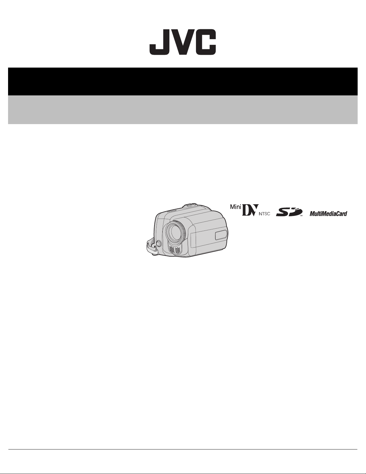
SERVICE MANUAL
DIGITAL VIDEO CAMERA
YF228<Rev.001>20082SERVICE MANUAL
GR-D850UC, GR-D850US,
GR-D870UC, GR-D870US,
GR-D875US
GR-D850UCM,GR-D850USM [M8D523]
GR-D870UCM,GR-D870USM
COPYRIGHT© 2008 Victor Company of Japan, Limited
Lead free solder used in the board (material : Sn-Ag-Cu, melting point : 219 Centigrade)
GR-D875USM [M8D525]
TABLE OF CONTENTS
1 PRECAUTIONS . . . . . . . . . . . . . . . . . . . . . . . . . . . . . . . . . . . . . . . . . . . . . . . . . . . . . . . . . . . . . . . . . . . . . . . 1-3
2 SPECIFIC SERVICE INSTRUCTIONS . . . . . . . . . . . . . . . . . . . . . . . . . . . . . . . . . . . . . . . . . . . . . . . . . . . . . . 1-5
3 DISASSEMBLY . . . . . . . . . . . . . . . . . . . . . . . . . . . . . . . . . . . . . . . . . . . . . . . . . . . . . . . . . . . . . . . . . . . . . . . 1-6
4 ADJUSTMENT . . . . . . . . . . . . . . . . . . . . . . . . . . . . . . . . . . . . . . . . . . . . . . . . . . . . . . . . . . . . . . . . . . . . . . . 1-33
5 TROUBLE SHOOTING. . . . . . . . . . . . . . . . . . . . . . . . . . . . . . . . . . . . . . . . . . . . . . . . . . . . . . . . . . . . . . . . . 1-36
COPYRIGHT© 2008 Victor Company of Japan, Limited
No.YF228<Rev.001>
2008/2
Page 2
SPECIFICATION
Camcorder
For General Power supply DC 11 V (Using AC Adapter)
DC 7.2 V (Using battery pack)
Power consumption Approx. 2.4 W (2.6 W*) (LCD monitor off, viewfinder on)
Approx. 7.5 W (Maximum; when charging the battery pack)
* Using LED Light
** The LCD Backlight is set to [STANDARD] mode.
Dimensions (W × H × D) 68 mm × 74 mm × 118 mm(2.68" × 2.91" × 4.65")
Weight Approx. 420 g (0.93 lbs) (without battery, cassette and lens cap)
GR-D850 Approx. 485 g (1.07lbs) (incl. battery, cassette and lens cap)
GR-D870 Approx. 490 g (1.08lbs) (incl. battery, cassette and lens cap)
Operating temperature 0°C to 40°C (32°F to 104°F)
Operating humidity 35% to 80%
Storage temperature -20°C to 50°C (-4°F to 122°F)
Pickup 1/6" CCD
Lens F1.8 to 4.0, f=2.2 mm to 77 mm, 35:1 power zoom lens
Filter diameter Ø30.5 mm
LCD monitor 2.7" diagonally measured, LCD panel/TFT active matrix system
Viewfinder Electronic viewfinder with 0.16" color LCD
Speaker Monaural
LED Light Effective distance: 1.5 m (5 ft)
For Digital Video
Camera
For Digital Still
Camera
* GR-D870only
For Connectors AV Video output 1.0 V (p-p), 75Ω, analog
Format DV format (SD mode)
Signal format NTSC standard
Recording/Playback
format
Cassette Mini DV cassette
Tape speed SP: 18.8 mm/s, LP: 12.5 mm/s
Maximum recording time
(using 80 min. cassette)
Storage media SD Memory Card/MultiMediaCard
Compression system JPEG (compatible)
File size Still image : 640 × 480 pixels
Picture quality 2 modes (FINE/STANDARD)
DV Input/output 4-pin, IEEE 1394 compliant
USB Mini USB-B type, USB 1.1 compliant
Video Digital component recording
Audio PCM digital recording, 32 kHz 4-channel (12-BIT), 48 kHz 2-channel (16-BIT)
SP: 80 min., LP: 120 min.
Audio output 300 mV (rms), 1 kΩ, analog, stereo
AC Adapter
Power requirement AC 110 V to 240 V, 50 Hz/60 Hz
Output DC 11 V, 1 A
Specifications shown are for SP mode unless otherwise indicated. E & O.E. Design and specifications subject to change without
notice.
1-2 (No.YF228<Rev.001>)
Page 3
SECTION 1
r
PRECAUTIONS
1.1 SAFTY PRECAUTIONS
Prior to shipment from the factory, JVC products are strictly
inspected to conform with the recognized product safety and
electrical codes of the countries in which they are to be
sold.However,in order to maintain such compliance, it is equally
important to implement the following precautions when a set is
being serviced.
1.1.1 Precautions during Servicing
(1) Locations requiring special caution are denoted by labels
and inscriptions on the cabinet, chassis and certain parts of
the product.When performing service, be sure to read and
comply with these and other cautionary notices appearing
in the operation and service manuals.
(2) Parts identified by the symbol and shaded ( ) parts
are critical for safety.
Replace only with specified part numbers.
NOTE :
Parts in this category also include those specified to
comply with X-ray emission standards for products
using cathode ray tubes and those specified for
compliance with various regulations regarding
spurious radiation emission.
(3) Fuse replacement caution notice.
Caution for continued protection against fire hazard.
Replace only with same type and rated fuse(s) as
specified.
(4) Use specified internal wiring. Note especially:
• Wires covered with PVC tubing
• Double insulated wires
• High voltage leads
(5) Use specified insulating materials for hazardous live parts.
Note especially:
• Insulation Tape
• PVC tubing
•Spacers
• Insulation sheets for transistors
•Barrier
(6) When replacing AC primary side components (transformers,
power cords, noise blocking capacitors, etc.) wrap ends of
wires securely about the terminals before soldering.
emission. Consequently, when servicing these products,
replace the cathode ray tubes and other parts with only the
specified parts. Under no circumstances attempt to modify
these circuits.Unauthorized modification can increase the
high voltage value and cause X-ray emission from the
cathode ray tube.
(12) Crimp type wire connectorIn such cases as when replacing
the power transformer in sets where the connections
between the power cord and power trans former primary
lead wires are performed using crimp type connectors, if
replacing the connectors is unavoidable, in order to prevent
safety hazards, perform carefully and precisely according
to the following steps.
• Connector part number :E03830-001
• Required tool : Connector crimping tool of the proper
type which will not damage insulated parts.
• Replacement procedure
a) Remove the old connector by cutting the wires at a
point close to the connector.Important : Do not
reuse a connector (discard it).
cut close to connector
Fig.1-1-3
b) Strip about 15 mm of the insulation from the ends
of the wires. If the wires are stranded, twist the
strands to avoid frayed conductors.
15 mm
Fig.1-1-4
c) Align the lengths of the wires to be connected.
Insert the wires fully into the connector.
Metal sleeve
Fig.1-1-1
(7) Observe that wires do not contact heat producing parts
(heatsinks, oxide metal film resistors, fusible resistors, etc.)
(8) Check that replaced wires do not contact sharp edged or
pointed parts.
(9) When a power cord has been replaced, check that 10-15
kg of force in any direction will not loosen it.
Power cord
Fig.1-1-2
(10) Also check areas surrounding repaired locations.
(11) Products using cathode ray tubes (CRTs)In regard to such
products, the cathode ray tubes themselves, the high
voltage circuits, and related circuits are specified for
compliance with recognized codes pertaining to X-ray
Connector
Fig.1-1-5
d) As shown in Fig.1-1-6, use the crimping tool to crimp
the metal sleeve at the center position. Be sure to
crimp fully to the complete closure of the tool.
1.2
5
2.0
5.5
Crimping tool
Fig.1-1-6
e) Check the four points noted in Fig.1-1-7.
Not easily pulled free
Wire insulation recessed
more than 4 mm
Crimped at approx. cente
of metal sleeve
Conductors extended
Fig.1-1-7
(No.YF228<Rev.001>)1-3
Page 4
1.1.2 Safety Check after Servicing
Examine the area surrounding the repaired location for damage
or deterioration. Observe that screws, parts and wires have been
returned to original positions, Afterwards, perform the following
tests and confirm the specified values in order to verify
compliance with safety standards.
(1) Insulation resistance test
Confirm the specified insulation resistance or greater
between power cord plug prongs and externally exposed
parts of the set (RF terminals, antenna terminals, video and
audio input and output terminals, microphone jacks,
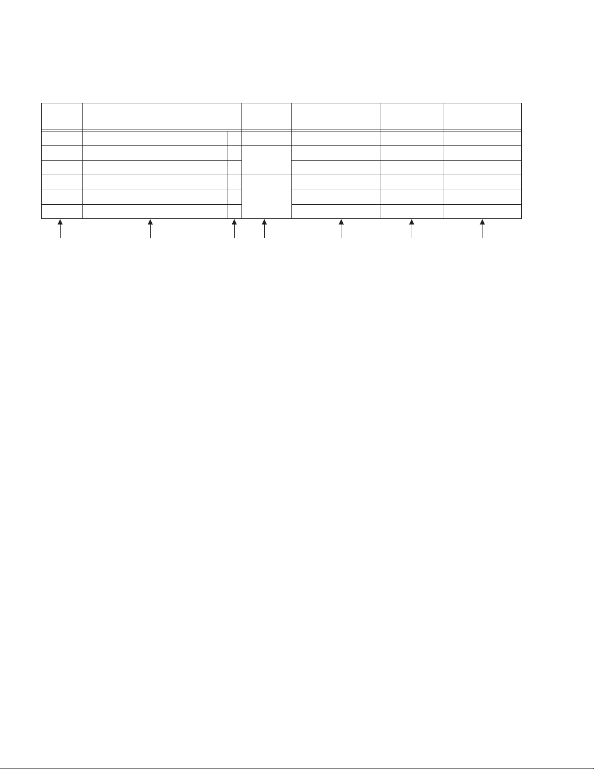
earphone jacks, etc.).See table 1 below.
(2) Dielectric strength test
Confirm specified dielectric strength or greater between
power cord plug prongs and exposed accessible parts of
the set (RF terminals, antenna terminals, video and audio
input and output terminals, microphone jacks, earphone
jacks, etc.). See Fig.1-1-11 below.
(3) Clearance distance
When replacing primary circuit components, confirm
specified clearance distance (d), (d') between soldered
terminals, and between terminals and surrounding metallic
parts. See Fig.1-1-11 below.
d
d'
Chassis
Power cord
primary wire
Fig.1-1-8
(4) Leakage current test
Confirm specified or lower leakage current between earth
ground/power cord plug prongs and externally exposed
accessible parts (RF terminals, antenna terminals, video
and audio input and output terminals, microphone jacks,
earphone jacks, etc.).
Measuring Method : (Power ON)Insert load Z between
earth ground/power cord plug prongs and externally
exposed accessible parts. Use an AC voltmeter to
measure across both terminals of load Z. See Fig.1-1-9
and following Fig.1-1-12.
ab
Externally
exposed
accessible part
Z
V
c
A
Fig.1-1-9
(5) Grounding (Class 1 model only)
Confirm specified or lower grounding impedance between
earth pin in AC inlet and externally exposed accessible
parts (Video in, Video out, Audio in, Audio out or Fixing
screw etc.).Measuring Method:
Connect milli ohm meter between earth pin in AC inlet and
exposed accessible parts. See Fig.1-1-10 and grounding
specifications.
AC inlet
Earth pin
Exposed accessible part
MIlli ohm meter
Grounding Specifications
Region
USA & Canada
Europe & Australia
Grounding Impedance (Z
Z 0.1 ohm
Z 0.5 ohm
)
Fig.1-1-10
AC Line Voltage
100 V
100 to 240 V
110 to 130 V
110 to 130 V
200 to 240 V
Region
Japan
USA & Canada
Europe & Australia
Insulation Resistance (R
R 1 M /500 V DC
1 M R 12 M /500 V DC
R 10 M /500 V DC
)
Dielectric Strength
AC 1 kV 1 minute
AC 1.5 kV 1 minute
AC 1 kV 1 minute
AC 3 kV 1 minute
AC 1.5 kV 1 minute
(
Class
(
Class
Clearance Distance (d), (d'
d, d' 3 mm
d, d' 4 mm
d, d' 3.2 mm
d 4 m m
)
d' 8 m m (Power cord
d' 6 m m (Primary wire
)
Fig.1-1-11
AC Line Voltage
100 V
110 to 130 V
110 to 130 V
220 to 240 V
Region
Japan
USA & Canada
Europe & Australia
Load Z
1
0.15
1.5
2
50
Leakage Current (i)
i 1 mA rms
i 0.5 mA rms
i 0.7 mA peak
i 2 mA dc
i 0.7 mA peak
i 2 mA dc
a, b, c
Exposed accessible parts
Exposed accessible parts
Antenna earth terminals
Other terminals
Fig.1-1-12
NOTE :
These tables are unofficial and for reference only. Be sure to confirm the precise values for your particular country and locality.
)
)
)
1-4 (No.YF228<Rev.001>)
Page 5
SECTION 2
SPECIFIC SERVICE INSTRUCTIONS
2.1 DIFFERENCE LIST
The following table indicate main different points between models GR-D850UC, GR-D850US, GR-D870UC, GR-D870US,
and GR-D875US.
MODEL NAME GR-D850UC GR-D850US GR-D870UC
DSC
CD-ROM NO NO YES
USB CABLE/TERMINAL NO NO YES
REMOTE CONTROL UNIT NO NO NO
MODEL NAME GR-D870US GR-D875US
DSC
CD-ROM YES YES
USB CABLE/TERMINAL YES YES
REMOTE CONTROL UNIT NO YES(RM-V740US)
NO NO YES
YES YES
(No.YF228<Rev.001>)1-5
Page 6
SECTION 3
DISASSEMBLY
3.1 BEFORE ASSEMBLY AND DISASSEMBLY
3.1.1 Precautions
• Be sure to disconnect the power supply unit prior to mounting
and soldering of parts.
• Prior to removing a component part that needs to disconnect
its connector(s) and its screw(s), first disconnect the wire(s)
from the connector(s), and then remove the screw(s).
• When connecting/disconnecting wires, pay enough attention
not to damage the connectors.
• When inserting the flat wire to the connector, pay attention to
the direction of the flat wire.
• Be careful in removing the parts to which some spacer or
shield is attached for reinforcement or insulation.
• When replacing chip parts (especially IC parts), first remove
the solder completely to prevent peeling of the pattern.
• Tighten screws properly during the procedures. Unless
otherwise specified, tighten screws at a torque of 0.088N
·cm). However, as this is a required value at the time of
(0.9kgf
·m
production, use the value as a measuring stick when
proceeding repair services. (See "SERVICE NOTE(1)" as for
tightening torque.)
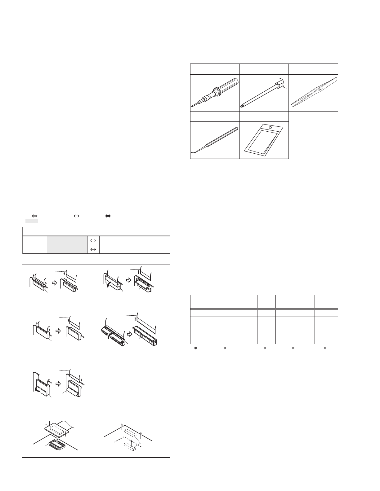
3.1.2 Destination of connectors
Two kinds of double-arrows in connection tables respectively
show kinds of connector/wires.
: Wire: Flat wire : Board to board (B-B)
: The connector of the side to remove
CONN. No. PIN No.CONNECTOR
CN2a
CN2b
MAIN CN101
MAIN CN103
MONI BW CN761
MINI BW CN762
40
10
3.1.3 Disconnection of connectors (Wires)
Wire
· Pull both ends of the connector in the arrow
direction, remove the lock and disconnect the flat
wire.
· Pull the both ends of the board in the direction
of the arrow, and remove the B-B Connector.
· Extend the locks in the direction of the arrow for
unlocking and then pull out the wire. After
removing the wire, immediately restore the locks
to their original positions because the locks are
apt to come off the connector.
B-B Connector
B-B Connector
· Pull the both ends of the board in the direction of the arrow, and remove the B-B Connector.
FPC Connector
Wire
FPC Connector
Wire
Lock
FPC Connector
· Extend the locks in the direction of the arrow for
unlocking and then pull out the wire. After
removing the wire, immediately restore the locks
to their original positions because the locks are
apt to come off the connector.
· Extend the locks in the direction of the arrow for
unlocking and then pull out the wire. After
removing the wire, immediately restore the locks
to their original positions because the locks are
apt to come off the connector.
Wire
FPC Connector
Wire
FPC Connector
Lock
Lock
Lock
B-B Connector
Fig.3-1-1
3.1.4 Tools required for disassembly and assembly
Torque driver
YTU94088
Chip IC replacement jig
PTS40844-2
Bit
YTU94088-003
Cleaning cloth
KSMM-01
Tweezers
P-895
Fig.3-1-2
• Torque driver
Be sure to use to fastening the mechanism and exterior parts because those parts must strictly be controlled for tightening torque.
• Bit
This bit is slightly longer than those set in conventional torque
drivers.
• Tweezers
To be used for removing and installing parts and wires.
• Chip IC replacement jig
To be used for replacement of IC.
• Cleaning cloth
Recommended cleaning cloth to wipe down the video heads,
mechanism (tape transport system), optical lens surface.
3.2 ASSEMBLY AND DISASSEMBLY OF MAIN PARTS
3.2.1 Assembly and disassembly
When reassembling, perform the step(s) in reverse order.
STEP
No.
[1]
[2]
PART
TOP COVER ASSY
UPPER ASSY
(Inc. VF ASSY,
SPEAKER/MONITOR)
[8]
E.VF UNIT(B/W)
(∗1) Order of steps in Procedure
When reassembling, preform the step(s) in the reverseorder.
These numbers are also used as the identification (location)
No. of parts Figures.
(∗2) Part to be removed or installed.
(∗3) Fig. No. showing Procedure or Part Location.
(∗4) Identification of part to be removed, unhooked, unlocked,
released, unplugged, unclamped or unsoldered.
S = Screw L = Lock, Release, Hook
SD = Solder CN = Connector
[Example]
• 4 (S1a) = Remove 4 S1a screws.
• 3 (L1a) = Disengage 3 L1a hooks.
• 2 (SD1a) = Unsolder 2 SD1a points.
• CN1a = Remove a CN1a connector.
(∗5) Adjustment information for installation.
Fig.
No.
4(S1a), 3(L1a),CN1a
C1
(S2a),2(S2b),3(S2c)
C2-1
2(SD1a),
L2,CN2a,b
2(S8),L8,CN8a
C2-2
POINT
( 4) ( 5)( 2) ( 3)( 1)
NOTE
-
-
NOTE 8
1-6 (No.YF228<Rev.001>)
Page 7
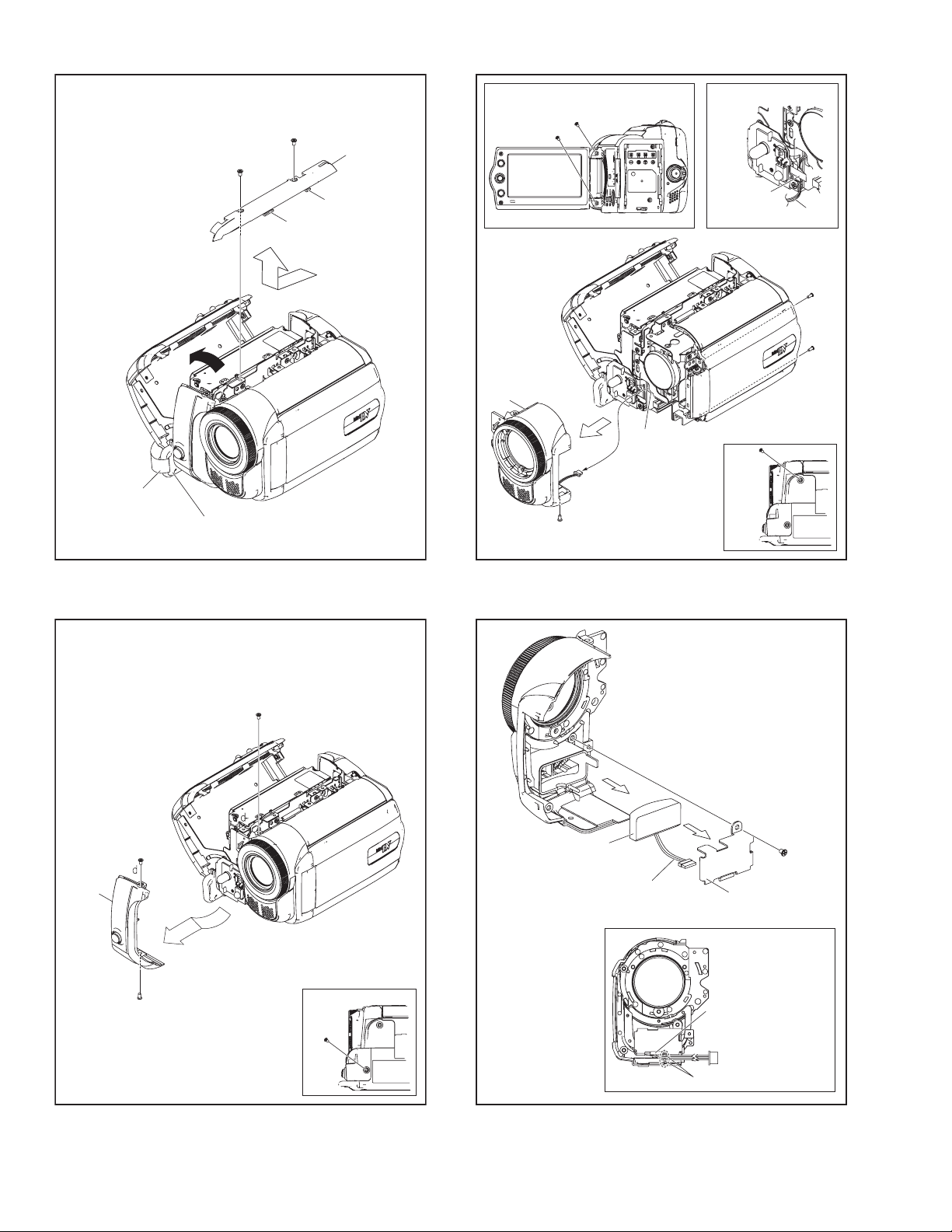
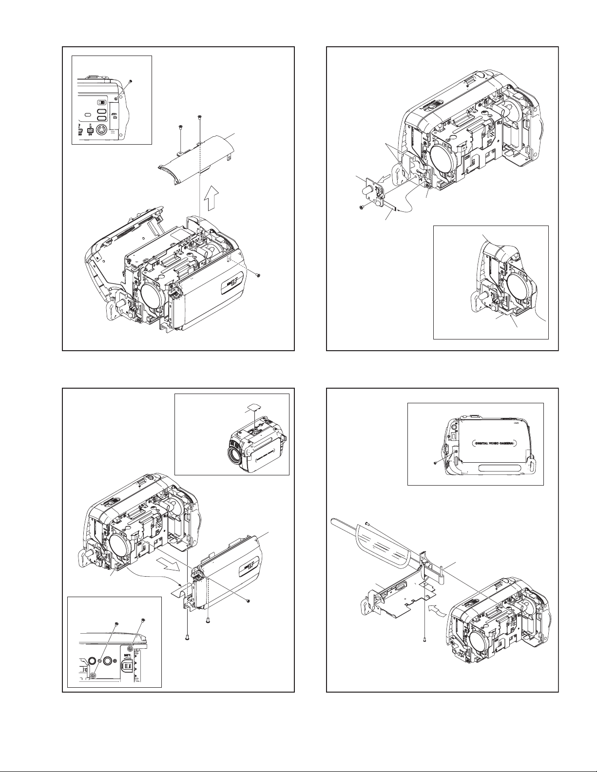
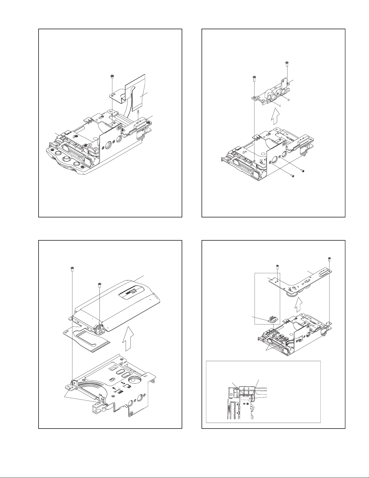
3.2.2 Assembly/Dissambly of cabinet parts and electrical parts
zDisassembly procedure
STEP
PART NAME
No.
[1]
COVER(LAST)
[2]
LOWER CASE(FRO) ASSY
[3]
FRONT CAVER ASSY
[4]
MIC
[5]
TOP COVER ASSY
[6]
UPPER ASSY
[7]
FRONT BOARD ASSY
[8]
LOWER CASE ASSY
[9]
CASSETTE COVER(SIDE)
[10]
CASSETTE COVER(TOP)
[11]
REAR ASSY
[12]
REAR BOARD ASSY
[13]
LOWER CASE(P) ASSY
[14]
OP BLOCK ASSY
[15]
ARM ASSY
[16]
MAIN BOARD ASSY
[17]
MECHANISM ASSY
[18]
MONITOR ASSY
[19]
TRIPOD(BASE)
[20]
JACK BOARD ASSY
Fig.
No.
3-2-1
3-2-2
3-2-3
3-2-4
3-2-5
3-2-6
3-2-7
3-2-8A
3-2-8B
3-2-9
3-2-10A
3-2-10B
3-2-11
3-2-12
3-2-13
3-2-14
3-2-15
3-2-16A
3-2-17
3-2-18A
3-2-18B
3-2-19
3-2-20
POINT NOTE
GRIP BELT,2(S1),L1a,b
3(S2)
2(S3a),S3b,CN3
S4
S5a,2(S5b)
COVER(JIG),S6a,b,c,CN6
S7,2(L7),CN7
S8a,b
-
2(S9),6(L9)
2(S10a)
S10b
2(S11),L11a,b,CN11a,b
S12,CN12
S13,L13a,b
CN14a,3(S14),L14,CN14b
4(S15),L15
CN16a,b,c,d,e,L16a,b
4(S17)
S18a,CN18
2(S18b),2(L18)
S19a,3(S19b)
S20a,b,2(L20)
NOTE1
-
NOTE3
NOTE4
-
NOTE6a,b
NOTE7
NOTE8a
NOTE8b
-
NOTE10a
NOTE10b,c
NOTE11a,b
NOTE12
NOTE13a,b
NOTE14a,b
NOTE15a,b
NOTE16
-
NOTE18a
NOTE18b
-
NOTE20a,b
NOTE1:
Pull out the GRIP BELT from the HOOK first as it interferes
with the procedure.
NOTE3:
When attaching, be careful with the wiring.
After connecting the wire to the connector, locate the wire
behind the FPC.
NOTE4:
When attaching, be careful with the wiring (MIC).
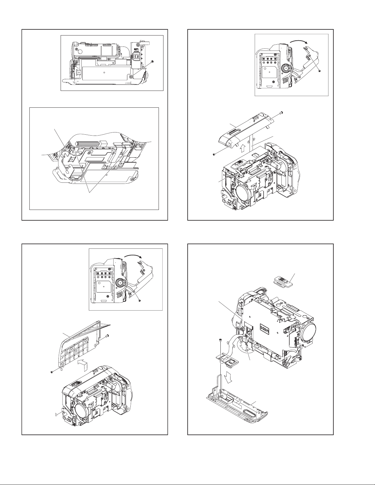
NOTE6a:
When removing, remove the COVER (JIG) first.
NOTE6b:
Please refer to Fig.3-2-18A and the following procedure for
removing the UPPER ASSY.
NOET7:
When attaching, be careful with the wiring.
NOTE8a:
During the procedure, be careful in handling the parts.
When the LOWER CASE ASSY is removed, the SHAFT
may come off.
NOTE8b:
When attaching, be careful with the FPC.
NOET10a:
During the procedure, be careful in handling the parts.
Be careful in handling the FPC as the switch connected to the
FPC is screwed on the back of the CASSETTE COVER (TOP).
NOET10b:
Be careful not to lose the KNOB (EJECT), or remove the
KNOB (EJECT) during the following procedures as it is easily
comes off when the CASSETTE COVER (TOP) is removed.
NOET10c:
When removing, carefully peel off and release the FPC as it
sticks to the ARM ASSY.
NOTE11a:
When attaching, be careful with the FPC.
NOTE11b:
When attaching, close the ARM ASSY.
When attaching, be careful with the wiring.
NOTE12:
When attaching, be careful with the wiring.
NOTE13a:
When removing, remove the screw (No.27) located under
the COVER (JACK) first.
NOTE13b:
When removing, be careful not to damage the HOOK (L13b).
NOTE14a:
When removing, the brackets are attached to the OP
BLOCK ASSY. During the procedure, remove the brackets
if necessary.
NOTE14b:
Refer to 3.2.3 Assembly/Disambly of [14] OP BLOCK ASSY/
CCD BOARD ASSYof OP BLOCK ASSY.
NOTE15a:
When removing, remove the 4 screws (No.31-34), and then
release the HOOK.
NOTE15b:
During the procedure, be careful with the grease applied to
the both sides.
NOTE16:
When attaching, be careful with the FPC.
NOTE18a:
Pay special attention in handling the removed UPPER
ASSY as the FPC is unstable.
NOTE18b:
Refer to 3.2.4 Disassembly of [18] MONITOR ASSY of
MONITOR ASSY.
NOTE20a:
When removing, be careful in handling the KNOB (SLIDE)
as they may come off.
NOTE20b:
When attaching, make sure that the LEVER of the SW interlocks with the KNOB (SLIDE).
zDestination of connectors
CN.
No.
CONNECTOR
PIN
No.
CN3 MAIN CN2601 MIC - 4
CN6 MAIN CN103
JACK/MONITOR
CN401/CN7002 50/24,28
CN7 MAIN CN108 FRONT CN801 8
CN11a MAIN CN101/CN106
CN11b MAIN CN105
REAR
CN501/CN504 40/32
POWER/ZOOM UNIT
- 12
CN14a MAIN CN4201 CCD CN5001 20
CN14b MAIN CN4901 OP BLOCK ASSY
- 25
CN16a MAIN CN1604 SENSOR - 16
CN16b MAIN CN1603 CAPSTAN MOTOR
- 18
CN16c MAIN CN1602 DRUM MOTOR - 11
CN16d MAIN CN3501 HEAD - 8
CN16e MAIN CN1601
/ROTARY ENCODER
LOADING MOTOR
8
-
CN18 JACK CN401 MONITOR CN7002 24
(No.YF228<Rev.001>)1-7
Page 8
1
(S1)
2
(S1)
[1]
7
(S3a)
6
(S3a)
NOTE3
GRIP BELT
NOTE1
HOOK
Fig.3-2-1
L1a
L1b
[3]
8
(S3b)
CN3
NOTE3
Fig.3-2-3
FPC
WIRE
6
(S3a)
7
(S3a)
8
(S3b)
[2]
5
(S2)
3
(S2)
4
(S2)
Fig.3-2-2
3
(S2)
[4]
NOTE4
WIRE(MIC)
9
(S4)
PLATE(MIC)
NOTE4
Slot WIRE(MIC) between
these bosses.
BOSS
Fig.3-2-4
1-8 (No.YF228<Rev.001>)
Page 9
10
(S5a)
11
(S5b)
12
(S5b)
[5]
L7
[7]
Fig.3-2-5
NOTE6a
COVER(JIG)
10
(S5a)
16
(S7)
FPC
NOTE7
CN7
NOTE7
FPC
Dress FPC as shown in figure.
Fig.3-2-7
17
(S8a)
CN6
(S6b)
14
13
(S6a)
13
(S6a)
Fig.3-2-6
14
(S6b)
NOTE6b
[6]
15
(S6c)
17
(S8a)
NOTE8a
SHAFT
[8]
18
(S8b)
Fig.3-2-8A
(No.YF228<Rev.001>)1-9
Page 10
NOTE8b
Ensure this part of LOWER CASE is on top of FRAME ASSY.
18
(S8b)
21
(S10a)
21
(S10a)
[10]
NOTE10a
FPC
Fold the MECHA FPC towards LOWER SIDE
when attaching LOWER CASE ASSY.
Fig.3-2-8B
L9
[9]
19
(S9)
19
(S9)
22
(S10a)
c
c
ARM ASSY
23
(S10b)
Fig.3-2-10A
KNOB(EJECT)
NOTE10b
20
(S9)
1-10 (No.YF228<Rev.001>)
Fig.3-2-9
FPC
NOTE10c
[10]
Fig.3-2-10B
Page 11
24
(S11)
25
(S11)
ARM ASSY
NOTE11a
FPC
L11b
CN11a
CN11b
Fig.3-2-11
[11]
L11a
24
(S11)
(S11)
SW(EJECT)
NOTE11b
CN11a
CN11b
25
27
(S13)
NOTE13a
[13]
Fig.3-2-13
REAR COVER
ASSY
NOTE13b
L13b
L13a
NOTE12
BOSS
[12]
WIRE
NOTE12
CN12
26
(S12)
CN14b
L14
30
(S14)
CN14a
29
(S14)
28
(S14)
[14]
NOTE14a,b
Fig.3-2-12
Fig.3-2-14
(No.YF228<Rev.001>)1-11
Page 12
NOTE15a
[15]
31
(S15)
NOTE16
33
(S15)
34
(S15)
g
32
(S15)
33
(S15)
34
(S15)
NOTE15b
35
(S16)
Fig.3-2-15
NOTE16
[16]
CN16e
g
A
CN16d
CN16a
B
C
CN16c
L16b
E
D
CN16b
L15
CN16a
(S17)
CN16b CN16c CN16d CN16e
Fig.3-2-16B
39
(S17)
36
37
(S17)
38
(S17)
AA
L16a
1-12 (No.YF228<Rev.001>)
E E
C
BB
Fig.3-2-16A
FRAME ASSY
HOOK
DD
[17]
Fig.3-2-17
Page 13
[18]
40
(S18a)
NOTE18a
FPC
CN18
43
(S19a)
44
(S19b)
(S19b)
[19]
45
46
(S19b)
L18
41
(S18b)
Fig.3-2-18A
42
(S18b)
NOTE18b
[18]
NOTE20b
NOTE20a
KNOB(SLIDE)
NOTE20b
LEVER
Fig.3-2-19
47
(S20a)
SW
L20
KNOB(SLIDE)
JACK
BOARD ASSY
48
(S20b)
[20]
Fig.3-2-18B
SW
Fig.3-2-20
(No.YF228<Rev.001>)1-13
Page 14
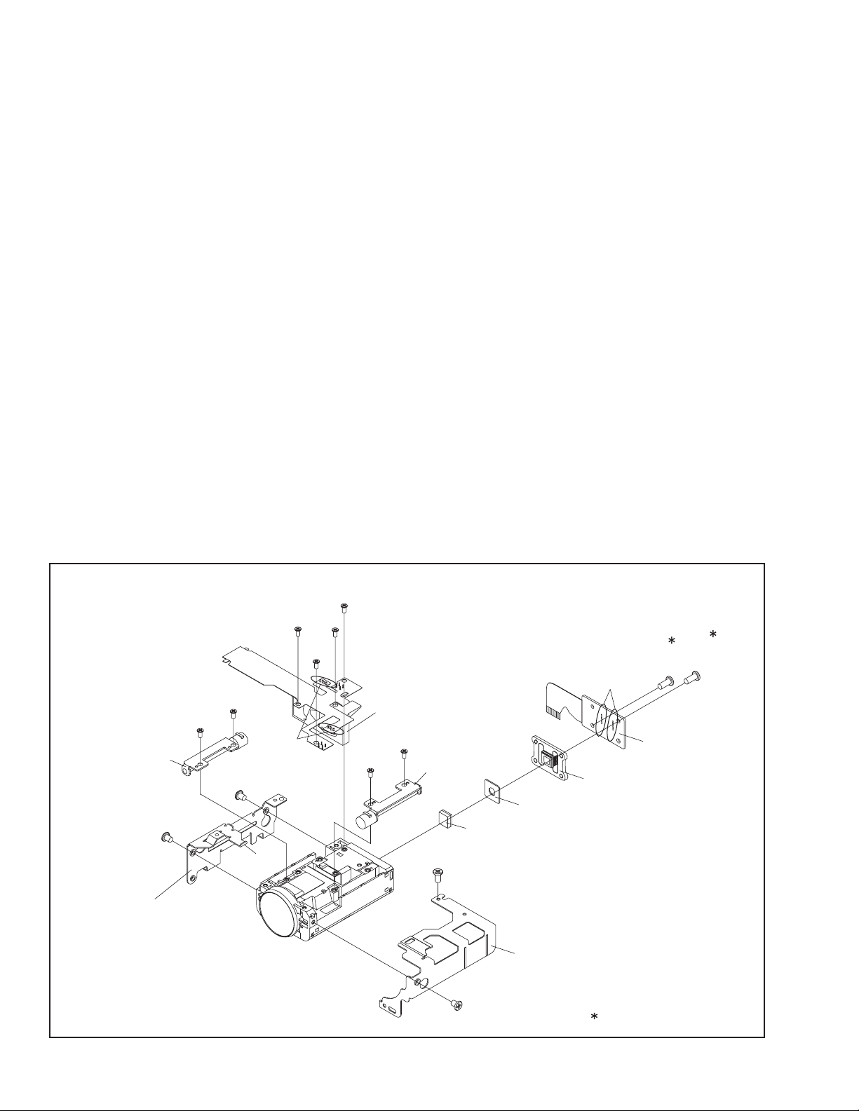
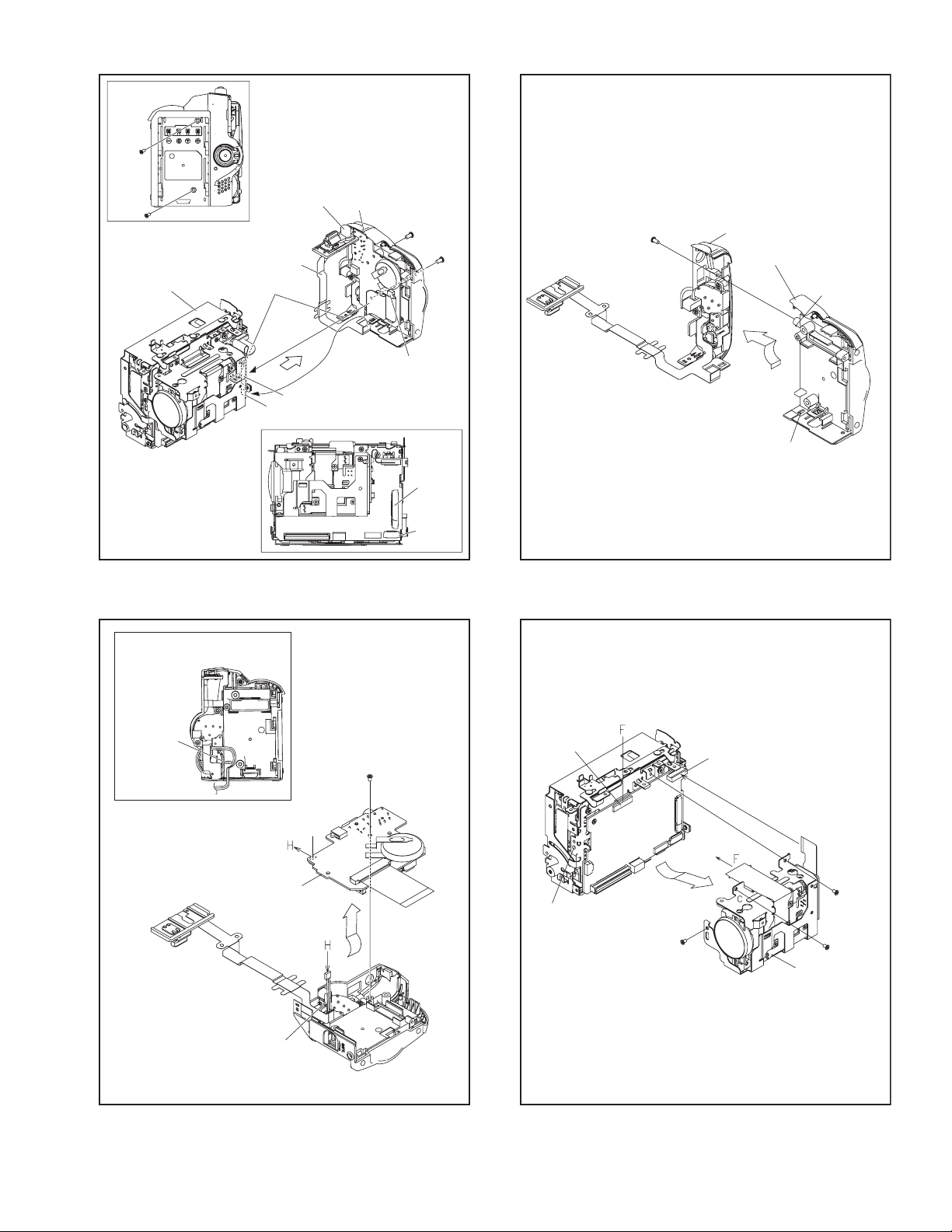
3.2.3 Assembly/Disambly of [14] OP BLOCK ASSY/CCD BOARD ASSY
zPrecautions
(1) Be careful in handling the CCD IMAGE SENSOR, OPTI-
CAL LPF and the LENS components. Pay special attention not to soil or damage the surfaces., especially with
regard to surface contamination, attached dust or
scratching. If fingerprints are present on the surface they
should be wiped away using either a silicon paper, clean
chamois or the cleaning cloth.
(2) The CCD IMAGE SENSOR may have been shipped with
a protective sheet attached to the transmitting glass.
When replacing the CCD IMAGE SENSOR, do not peel
off this sheet from the new part until immediately before
it is mounted in the OP BLOCK ASSY.
(3) As the CUSHION(OP) protects the OP BLOCK ASSY
from scratches or damages, leave the CUSHION as
long as it does not interfere with the procedure.
zDisassembly of OP BLOCK ASSEMBLY / CCD BOARD AS-
SEMBLY
(1) Unsolder the fourteen soldered points (SD11a) of the
CCD BOARD ASSY.
(2) Remove the two screws (1,2), and then remove the CCD
BOARD ASSY and the CCD BASE ASSY.
NOTE11a:
When removing the CCD BASE ASSY, be careful in
handling as the CCD IMAGE SENSOR may be removed together with the SHEET and the OP LPF attached.
NOTE11\b:
Replace the CCD IMAGE SENSOR as a CCD BASE
ASSY, not as a single part replacement.
zAssembly of OP BLOCK ASSEMBLY / CCD BOARD AS-
SEMBLY
(1) Set the OPTICAL LPF first, and then the SHEET to the
(2) Attach the CCD BASE ASSY first, then the CCD BASE
(3) Solder the 14 points (SD11a) on the CCD BOARD AS-
zReplacement of service repair parts
The service repair parts for the OP BLOCK ASSY are as listed
below.
When replacing the parts, remove the BKT OP (1) and (2) first
if necessary.
When replacing parts, be careful not to cut the FPCs or damage any parts by soldering (excessive heat).
(1) FOCUS MOTOR UNIT
(2) ZOOM MOTOR UNIT
(3) AUTO IRIS UNIT
NOTE 13e:
When replacing the FOCUS MOTOR UNIT or the ZOOM
MOTOR UNIT, solder the FPC at a space of about 0.5 mm
above the terminal pin.
NOTE 13f:
The IRIS MOTOR UNIT includes the FPC ASSY and two
sensors.
OP BLOCK ASSY.
NOTE11c:
Be careful with the attachment direction of the OP
LPF.
ASSY so that the SHEET stays in place, and then tighten
with the two screws (1, 2).
SY.
ZOOM MOTOR
UNIT
5
(S14c)
BKT OP(2) ASSY
9
(S14d)
10
(S14d)
6
(S14c)
HOOK
11
(S14d)
SD14b
13
(S14d)
12
(S14d)
14
(S14d)
(S14d)
NOTE14d
AUTO IRIS
UNIT
8
(S14d)
7
FOCUS MOTOR
UNIT
OP LPF
3
(S14c)
NOTE14c
SD14a
CCD BASE ASSY
NOTE14a,b
SHIEET
BKT OP(1) ASSY
1
(S14a)
CCD BOARD
ASSY
2
(S14a)
1-14 (No.YF228<Rev.001>)
Fig.3-2-21
4
(S14c)
:0.147 N・m (1.5kgf・cm)
Page 15

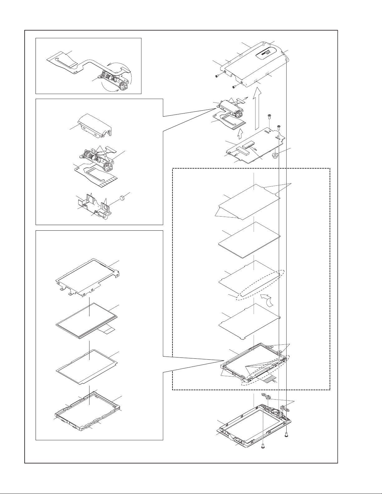
3.2.4 Disassembly of [18] MONITOR ASSY
zCAUTIONS
(1) During the procedure, be careful in handling the LCD
MODULE and other parts. Pay special attention not to
damage or soil the monitor screen.
If fingerprints are left on the screen, wipe them with clean
chamois leather or a cleaning cloth.
zRemoving MONITOR ASSEMBLY
(1) Remove the 2 screws (1 and 2).
(2) Turn the HINGE UNIT ASSY 90º, and remove the two
screws (3 and 4).
(3) Remove the MONITOR COVER ASSY by removing the
6 hooks (L18a-f).
(4) Release the lock of the connector (CN18a), and remove
the HINGE UNIT by lifting it up.
NOTE18a:
During the procedure, be careful in handling the FPC.
(5) Release the lock of the connector (CN18b), and pull out
the FPC.
(6) Remove the 2 screws (5 and 6), and remove the MONI-
TOR BOARD ASSY .
NOTE18b:
Be careful in handling as the parts located below may
be misaligned or removed when the MONITOR
BOARD ASSY is removed.
Attach the MONITOR BOARD ASSY by lifting up the
MONITOR CASE as the KNOB (CURSOR) that is attached to the BOARD sticks out toward the LCD
screen.
NOTE18c:
When replacing the MONITOR CASE or when there is
no need to replace individual parts in the MONITOR
CASE, remove the whole parts from the SHEET
(M.REF) to the LCD SA as a unit.
(7) Remove the SHEET (M.REF), LIGHT GUIDE, SHEET
(M/DIFF), and the SHEET(BEF)1.
NOTE18d:
When attaching, insert one side of the SHEET (M/
DIFF) under the LCD CASE RIB.
NOTE18e:
When attaching, insert each tab on both sides of the
SHEET (M.REF) into the LCD CASE notch.
(8) Remove the SHIELD CASE(MONI), LCD MODULE,
SHEET(COVER) and the LCD CASE.
NOTE18f:
During the procedure, handle the 4 parts (SHIELD
CASE(MONI), LCD MODULE, SHEET(COVER)) together.
zRemoving HINGE UNIT ASSEMBLY
(1) While removing the 6 HOOKs (L18t-w) from one side
and then from the other side, remove the HINGE COVER (U).
NOTE18g:
Be careful in handling the HINGE ASSY as grease is
applied inside.
(2) Remove the HINGE COVER(L).
(3) Remove the MAGNET.
NOTE18h:
During the procedure, be careful in handling the mag-
net.
When attaching, set the negative pole outside as
shown in the figure. Be careful when removing as
there is no marking.
NOTE18j:
During the procedure, be careful in handling the FPC.
NOTE18k:
The FPC is rolled around the axis of rotation of the
HINGE ASSY 2.5 rounds (2.5times).
The connecting side to the MONITOR BOARD ASSY
is placed inside.
(No.YF228<Rev.001>)1-15
Page 16
FPC
LIB
NOTE18d
HINGE ASSY
<HINGE UNIT ASSY>
H.COVER(U)
L18g
NOTE18j
FPC
H.COVER(L)
L18v
L18w
NOTE18k
NOTE18g
HINGE UNIT
NOTE18h
MAGNET
MONITOR COVER
ASSY
3
(S18b)
NOTE18g
HINGE UNIT
ASSY
FPC
NOTE18a
MONITOR
BOARD ASSY
CN18a
NOTE18c
SHEET
(M.REF)
L18a
a
4
(S18b)
L18g
L18h
[18]
L18b
L18f
L18e
L18d
b
C
C
L18c
5
(S18c)
B
CN18b
6
(S18c)
KNOB
(CURSOR)
L18j
NOTE18e
L18t
NOTE18f
<LCD SA>
L18s
L18r
L18q
L18u
SHILD CASE
(MONI)
LCD MODULE
SHEET(COVER)
L18t
LCD CASE
L18p
L18n
L18m
NOTE18e
L18k
LIGHT GUIDE
SHEET
(M/DIFF)
NOTE18d
SHEET
(BEF)1
NOTE18f
LCD SA
NOTE18e
MONITOR CASE
a
NOTE18d
NOTE18d
LIB
LIB
b
(S18a)
NOTE18e
B
BUTTON
(MONI)
NOTE18b
1
2
(S18a)
1-16 (No.YF228<Rev.001>)
Fig.3-2-22
Page 17
3.3 DVC MECHANISM
3.3.1 TOOLS REQUIRED FOR ADJUSTMENTS
1.
Torque driver
YTU94088
2.
Bit
YTU94088-003
1. Torque driver
Be sure to use to fastening the mechanism and exterior parts
because those parts must strictly be controlled for tightening
torque.
Torque setting value of torque driver is limited. At the values
over the maximum torque setting value, fasten a screw manually not to damage the screw thread.
3.
Tweezers
P-895
Chip IC replacement jig
4.
PTS40844-2
2. Bit
This bit is slightly longer than those set in conventional torque
drivers.
3. Tweezers
To be used for removing and installing parts and wires.
4. Chip IC replacement jig
5.
Guide driver
YTU94148A-1
6.
Cleaning cloth
KSMM-01
To be used for replacement of part.
5.Guide driver
To be used for the height adjustment such as the guide rollers.
6. Cleaning cloth
Recommended cleaning cloth to wipe down the video heads,
mechanism (tape transport system), optical lens surface.
3.3.2 Precautions
(1) When fastening parts, pay careful attention to the tightening torque of each screw. Unless otherwise specified, tighten a screw
with the torque of 0.055 N
·m (0.56 kgf·cm).
(2) Be sure to disconnect the set from the power supply before fastening and soldering parts.
(3) When disconnecting/connecting wires, be careful not to get them and their connectors damaged.
(4) When replacing parts, be very careful neither to damage other parts nor to fit wrong parts by mistake.
(No.YF228<Rev.001>)1-17
Page 18
3.3.3 Notes on procedure for disassembly/assembly
The DISASSEMBLY PROCEDURE TABLE shows the procedure to disassemble/reassemble mechanism parts.
Carefully read the following explanation before starting actual disassembling/reassembling work. The item numbers(circled numbers)in the following explanation correspond to those appearing under respective columns of the table.
Example
NO. PART NAME FIG. POINT NOTE REMARKS
[1]
[2]
[3]
[4]
[5]
[6]
*1 *2 *3 *4 *5 *6 *7
*1 Numbers appearing in this column indicate the order to re-
move parts. When reassembling, follow these numbers in
the reverse order. Circled numbers in this column correspond to those appearing in drawings of this section.
*2 This column shows part names corresponding to numbers
in the left column.
*3 The symbol (T or B)appearing in this column shows the
side which the objective part is mounted on.
T =the upper side, B =the lower side
*4 Symbols appearing in this column indicate drawing num-
bers.
*5 This column indicates parts and points such as screws,
washers,springs,and others to be removed/fitted for disassembling/reassembling the mechanism. Besides such the
parts, this column occasionally indicates working points.
P= Spring
W = Washer
S= Screw
* = Lock (L),soldering (SD),shield,connector (CN),etc.
CASSETTE HOUSING ASSY T Fig.2-4-3 3(S1),(L1a)-(L1e)
UPPER BASE ASSY T Fig.2-4-4 (S2),(L2a),(L2b)
DRUM ASSY T (S3a),2(S3b)
REEL DISK ASSY(SUP) T Fig.2-4-5 (W4)
REEL DISK ASSY(TU) T
REEL COVER ASSY T
(W5a),(W5b),(W5c)
(W6),(S6a),2(S6b)
*6 Numbers in this column represent the numbers of notes in
the text.
(For parts that need phase adjustment after reassembling,
refer to “MECHANISM ADJUSTMENTS”.)
*7 This column indicates required after-disassembling/-reas-
sembling work such as phase adjustment or mechanism
adjustment.
NOTE 1 a,b,c,d
NOTE 2
NOTE 3 a,b
NOTE 4 a
NOTE 5 a,b
NOTE 6
ADJUSTMENT
ADJUSTMENT
Example
• Remove (W1)=Washer W1.
• Remove the solder at (SD1)=Point SD1.
• Disconnect A = Connector A.
1-18 (No.YF228<Rev.001>)
Page 19
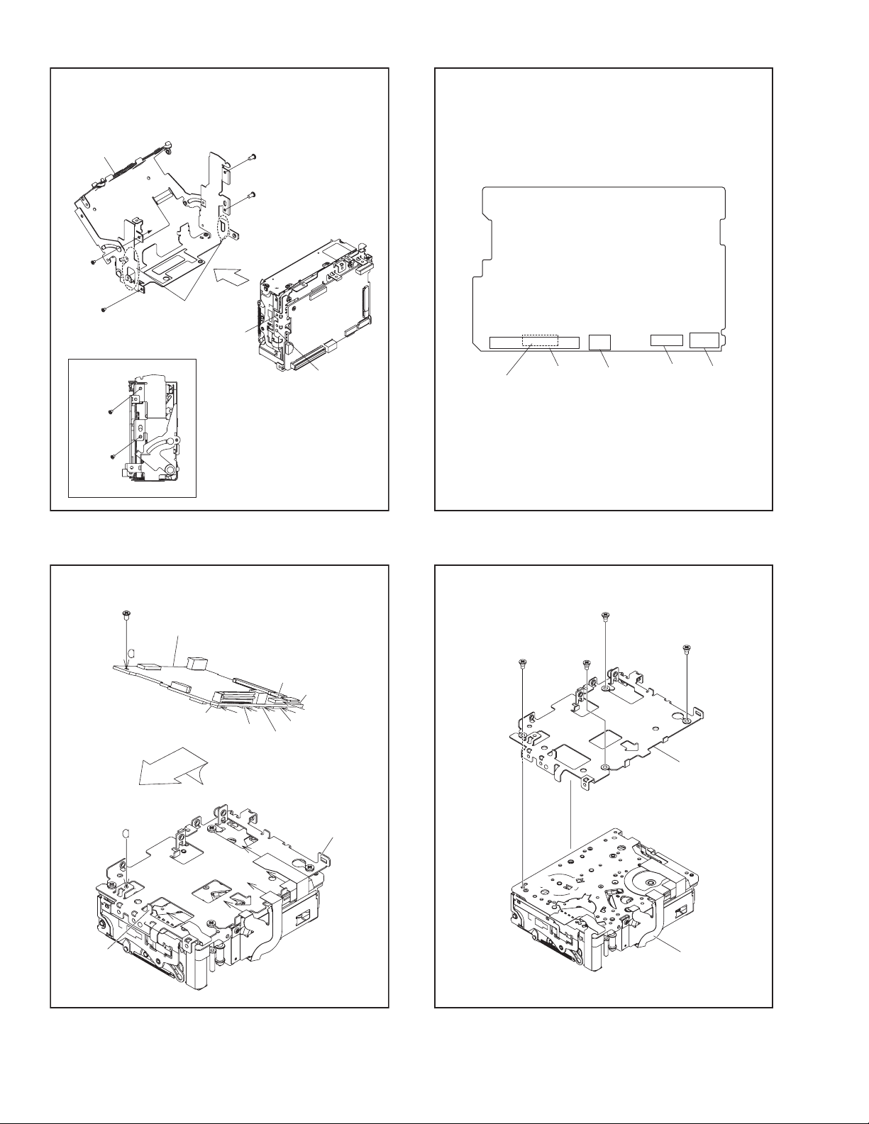
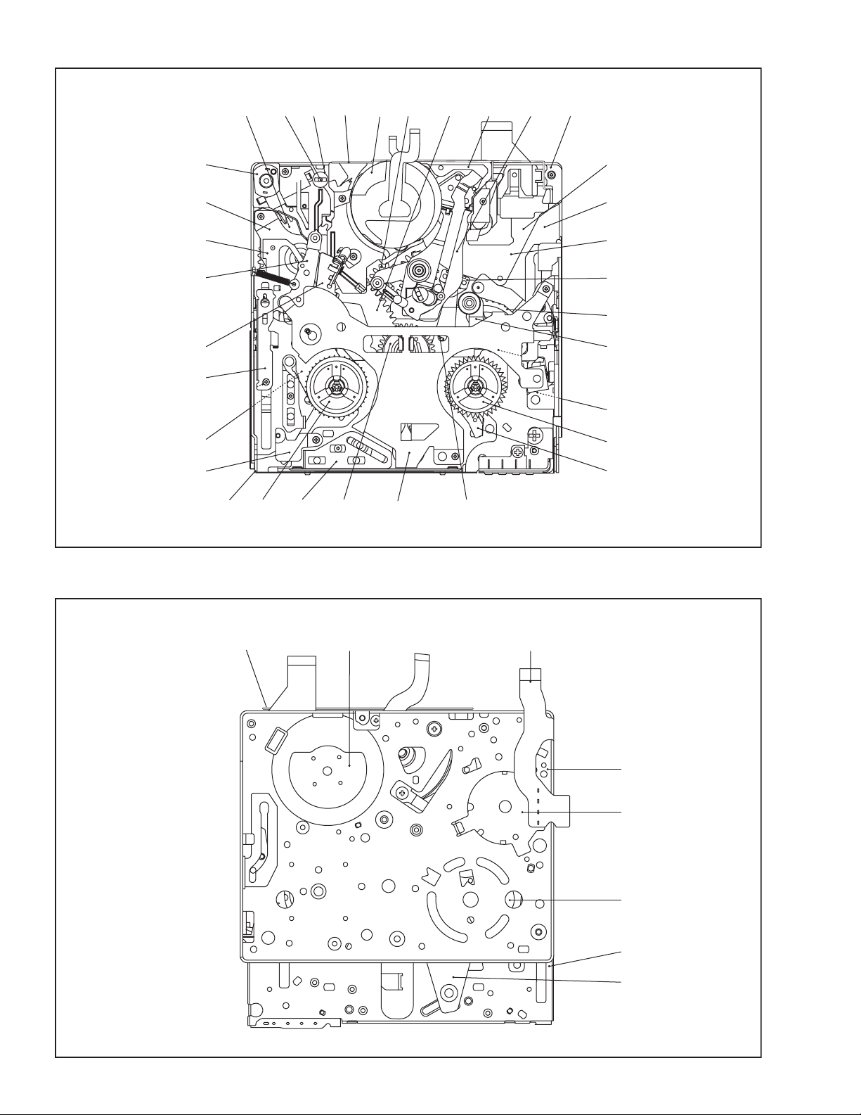
3.3.4 DISASSEMBLY AND ASSEMBLY OF MECHANISM ASSEMBLY
Half Panch
3.3.4.1 General statement
The mechanism should be disassembled/assembled in the
CASS IN mode (ASSEMBLY mode). (Refer to Fig. 3-3-2,3-3-5.)
When the mechanism assembly is removed from the main body,
it is generally set in the STOP mode.
After the mechanism assembly is removed from the main body,
it is required to forcibly supply 3V DC to the LOADING MOTOR
to unload, and then set the CASS IN mode.
<Mechanism assembly/Cassette housing assembly>
3.3.4.2 Mechanism modes
The mechanism mode of this model is classified into five modes
as shown in Fig. 3-3-9. Each mechanism mode can be distinguished from others by the relative position of “ ”, “ ”, “ ”
marks on the sub cam gear to the inner or outer protrusion on the
main deck. Refer to Fig. 3-3-3 to 3-3-8 below.
DC3V
<Confirmation of mode>
LOADING MOTOR
<MAIN CAM GEAR>
TOP VIEW BOTTOM VIEW
Fig.3-3-3
:HOLE(Penetration)
:Half Panch
<EJECT mode>
Fig.3-3-1
<Back side of the mechanism assembly>
CASS INOQFG
HOLE
Half Panch
Half Panch
Fig.3-3-4
<CASS IN mode>
Fig.3-3-5
<SHORT FF mode>
Fig.3-3-6
<STOP mode>
Back side of deck
Fig.3-3-2
Fig.3-3-7
<PLAY mode>
Fig.3-3-8
(No.YF228<Rev.001>)1-19
Page 20
3.3.4.3 Mechanism timing chart
PARTS
ROTARY
ENCODER
MAIN CAM
SUB CAM
PRESS ARM
T.C. PLATE
MODE
-69.2
a
b
c
PRESS
OFF
EJECT
OFF1
OFF2
EJECT CAS. IN
o
-68.4
o
-54.7
(-50
(-65
-40
o
)
-52
o
)
-49.2
o
o
o
o
-6.5
o
-46.3
-5.5
o
0
3.4
TU. P. B
END
182.8
SLIDE
END
187.8
STOP PLAYFWD
o
244.5
254.5
273.6
o
260
o
o
274.5
o
190
(200o)
o
247
(260o)
o
o
205.3
o
o
o
210.8
199.8
o
150
(149o)(126.9o)
o
195
(193.8o)(164.9o)
o
210.5
o
SHORT
SLIDE
49.3
o
START
(49.1
(63.8
o
78.3
90.3o101.3o113.3
o
)
o
)
95.8
70
91
o
o
o
o
CCW
o
o
o
5.5
o
0
o
0
o
TENSION ARM
T5 ARM
SLIDE DECK
S1 ARM
POLE BASE
PINCH ROLLER
ON
LO2
LO1
UL
ON
OFF
LO
UL
PRESS
LO
UL
PRESS
LO
UL
PRESS
SLIDE
OFF
3.4
o
69
o
67.2
o
o
79.6
o
67.2
o
67.2
o
14
o
67.2
o
67.2
127.8
o
o
204
o
204
o
204
o
164.2
TOUCH
173.6
TOUCH
o
204
o
204
o
o
244.5
o
225.5
o
220.2
TOUCH
o
204
Fig.3-3-9
1-20 (No.YF228<Rev.001>)
Page 21
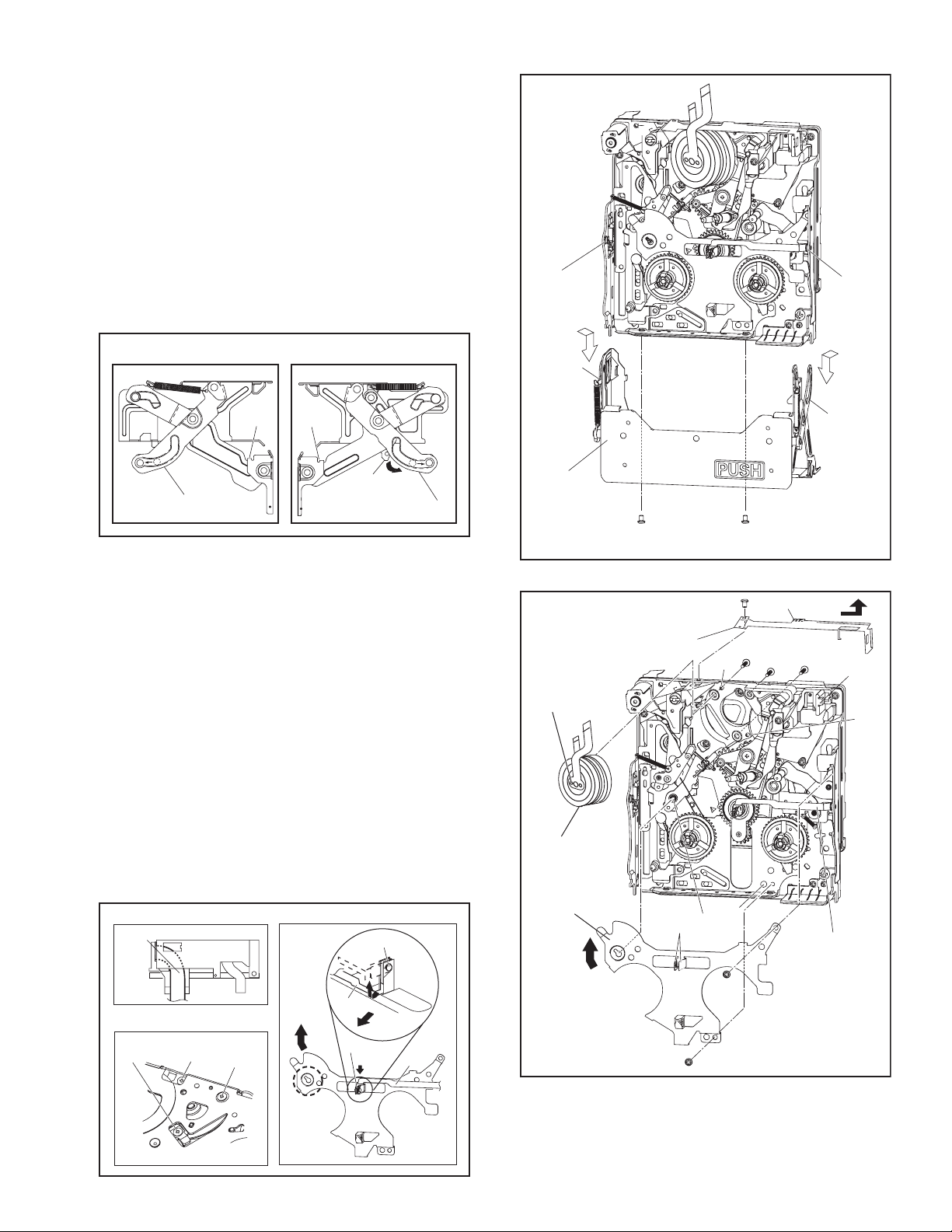
3.3.5 DISASSEMBLY PROCEDURE TABLE
MARK: # After assembly, perform adjustments.
NO. PART NAME FIG. POINT NOTE REMARKS
[1] HOUSING ASSY T 3-3-10 2(S1),L1a,b,c,d NOTE1a,b ADJUSTMENT
[2] DRUM PROTECTOR T 3-3-11 S2,L2a,b NOTE2
[3] DRUM ASSY T 3-3-11 3(S3),L3a,b NOTE3a,b #
[4] REEL COVER ASSY T 3-3-11 2(S4),2(L4a),L4b,c NOTE4
[5] IDLER ARM ASSY T 3-3-12 - -
[6] T5 ARM ASSY T 3-3-12 L6a,b NOTE6a,b ADJUSTMENT
[7] TENSION ARM ASSY T 3-3-12 L7a,S7,L7b,2(L7c) NOTE7a,b,c ADJUSTMENT/#
[8] S1 ARM ASSY T 3-3-13 L8 NOTE8 ADJUSTMENT
[9] SLIDE GUIDE PLATE T 3-3-13 S9,L9 NOTE9a,b ADJUSTMENT/#
[10] GUIDE PLATE T 3-3-13 S10,L10 - ADJUSTMENT
[11] SLIDE DECK ASSY T 3-3-14A 2(L11a),3(L11b),2(L11c) NOTE11a,b ADJUSTMENT/#
[12] CASSETTE GUIDE T 3-3-14B S12,2(L12) -
[13] PINCH ROLLER ARM ASSY T 3-3-14B L13 NOTE13a,b,c
[14] REEL DISK ASSY (SUP) T 3-3-14B L14 NOTE14a,b
[15] REEL DISK ASSY (TU) T 3-3-14B L15 NOTE15a,b,c
[16] BRAKE PLATE T 3-3-14B - NOTE16 ADJUSTMENT
[17] T. C. PLATE ASSY T 3-3-15 L17,SLIDE COLLAR1 NOTE17
[18] DRUM BASE T 3-3-15 3(S18),L18a,2(L18b) NOTE18
[19] DRIVE ARM ASSY T 3-3-15 L19,SLIDE COLLAR2 NOTE19a,b ADJUSTMENT
[20] GUIDE RAIL ASSY T 3-3-16 S20 NOTE20 ADJUSTMENT/#
[21] T5 CATCHER T 3-3-16 S21,L21 -
[22] CAPSTAN MOTOR T 3-3-16 2(S22) NOTE22
[23] REEL PULLEY T 3-3-16 - -
[24] CENTER GEAR T 3-3-16 - -
[25] MOTOR BRACKET ASSY T 3-3-17 S25 NOTE25a,b,c
[26] BELT GUIDE T 3-3-17 S26,2(L26) -
[27] GEAR COVER T 3-3-17 3(S27),L27a,b,c,d NOTE27 ADJUSTMENT
[28] PRESS ARM ASSY T 3-3-17 L28 NOTE28 ADJUSTMENT
[29] SUB CAM T 3-3-18 - NOTE29 PHASE ADJUSTMENT
[30] CONNECT GEAR T 3-3-18 - NOTE30
[31] MAIN CAM T 3-3-18 - NOTE31 PHASE ADJUSTMENT
[32] ROTARY ENCODER T 3-3-19 L32 NOTE32 PHASE ADJUSTMENT
[33] LOADING GEAR 1 T 3-3-19 - -
[34] GUIDE ROLLER (S) ASSY T 3-3-19 - NOTE34a,b #
[35] COMPRESSION SPRING T 3-3-19 - NOTE35
[36] MAIN DECK ASSY T 3-3-19 - - #
[ 1 ]
(No.YF228<Rev.001>)1-21
Page 22
< TOP VIEW >
[34] [35] [ 3 ]
[ 2 ][32] [33] [19] [18] [20] [21]
[25]
[27]
[17]
[ 7 ]
[ 8 ]
[10]
[31]
[12]
[22]
[36]
[ 6 ]
[26]
[29]
[30]
[28]
[15]
[16]
[14][11] [ 9 ] [ 5 ] [ 4 ] [30]
< BOTTOM VIEW >
[25][22][ 2 ]
[36]
[32]
[31]
[11]
[19]
1-22 (No.YF228<Rev.001>)
Page 23
3.3.6 DISASSEMBLY/ASSEMBLY
3.3.6.1 [1] HOUSING ASSY
NOTE1a:
When disassembling/ assembling the MECHANISM ASSY,
make sure to remove the HOUSING ASSY.
When removing the HOUSING ASSY, make sure to bring the
HOUSING ASSY up either by changing the mechanism mode
to the EJECT mode, or by moving the EJECT LEVER to the direction as indicated by the arrow.
During the procedure, make sure to return to the CASS IN
mode if the mode was changed.
NOTE1b:
Be careful not to damage the LEFT ARM2,RIGHT ARM2 during work.
<NOTE1a,b>
L1a L1b
L1c
LEFT
ARM2
NOTE1b
L1d
RIGHT
ARM2
NOTE1b
EJECT
LEFT ARM2
3.3.6.2 [2] DRUM PROTECTOR
[3] DRUM ASSY
[4] REEL COVER ASSY
NOTE2:
During the procedure, be careful in handling the FPC.
NOTE3a:
When removing, carefully hold the top center of the DRUM
ASSY with fingers otherwise it may possibly fall off.
NOTE3b:
Pay extra attention to the soil, dust and scratch on the surface.
During the procedure, be careful not to cut/ damage the FPC.
NOTE4:
During the procedure, remove the LED from the REEL COVER
ASSY first to set the FPC free, remove the two screws (7, 8),
then remove the REEL COVER ASSY by sliding it to the direction as indicated by the arrow.
During the procedure, be careful in handling the FPC.
LEVER
RIGHT ARM2
<NOTE2> <NOTE4>
FPC
LED
[ 1 ]
NOTE1a
NOTE3a
[3]
NOTE3b
[4]
1
(S1)
NOTE2
Fig.3-3-10
[2]
L4c
L4a
3
(S2)
L3a
L4b
2
(S1)
4
(S3)
L2a
5
(S3)
6
(S3)
L2b
L3b
FPC
NOTE4
<NOTE3a>
6
(S3)
(S3)
< bottom side >
7
FPC
DRUM
5
4
(S3)
LED
SIDE
FPC
8
(S4)
(S4)
Fig.3-3-11
(No.YF228<Rev.001>)1-23
Page 24
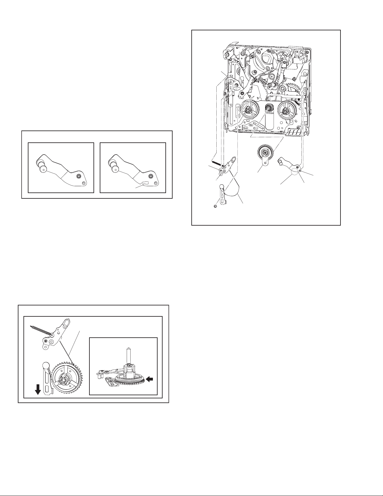
3.3.6.3 [5] IDLER ARM ASSY
L7c
[6] T5 ARM ASSY
[7] TENSION ARM ASSY
NOTE6a:
There are two types of the T5 ARM ASSY. They are different
in shape. The old type is without a hook and the new type is
with a hook.
When an old type is replaced by a new type, replace the
PINCH ROLLER ARM ASSY at the same time as the proper
combination of the parts is required.
When removing, remove the spring from the hook first if there
is a hook.
NOTE6b:
When mounting, pay attention to the correct positioning.
<NOTE6a>
< OLD TYPE > < NEW TYPE >
[7]
L7a
L7c
L7c
L6a
NOTE7a:
During the procedure, be careful in handling the TENSION
BAND.
NOTE7b:
When mounting, attach the TENSION BAND along the groove
of the gear.
NOTE7c:
When mounting, pay attention to the correct positioning.
When mounting, attach the TENSION ARM ASSY with the
plate moved to the direction as indicated by the arrow.
If the plate is moved to the other direction, the TENSION
BAND may break during the operation check as there is too
much tension.
After the mounting, adjust the TENSION ARM ASSY.
<NOTE7b,c>
< TOP >
TENSION BAND
< FRONT >
L7b
(S7)
[5]
NOTE6a
L6b
[6]
NOTE6b
9
TENSION BAND
NOTE7a
Fig.3-3-12
1-24 (No.YF228<Rev.001>)
Page 25
3.3.6.4 [8] S1 ARM ASSY
[9] SLIDE GUIDE PLATE
[10] GUIDE PLATE
NOTE8:
When mounting, pay attention to the correct positioning.
NOTE9a:
When mounting, pay attention to the correct positioning.
NOTE9b:
After attachment, adjust the SLIDE GUIDE PLATE.
L10
[10]
3.3.6.5 [11] SLIDE DECK ASSY
NOTE11a:
When removing, set the FPC free first.
During the procedure, be careful not to cut the FPC.
NOTE11b:
During the procedure, be careful in handling.
<NOTE11a>
L11c
T5 CATCHER
L11a
FPC
(S10)
[11]
11
L8
L11b
L9
[8]
NOTE8
Fig.3-3-13
L11b
FPC
10
(S9)
NOTE9a,b
NOTE11a
[9]
L11a
Fig.3-3-14A
L11c
NOTE11b
MIC SW
(No.YF228<Rev.001>)1-25
Page 26

3.3.6.6 [12]CASSETTE GUIDE
[13] PINCH ROLLER ASSY
[14] REEL DISK ASSY (SUP)
[15] REEL DISK ASSY (TU)
[16] BRAKE PLATE
NOTE13a:
The spring attachment differs according to the types of the T5 ARM
ASSY. The spring is attached either to the hook of the SLIDE
DECK ASSY or to the hook of the T5 ARM ASSY. When an old
type is replaced by a new type, replace the T5 ARM ASSY at the
same time as the proper combination of the parts is required.
When removing, remove the spring only when the spring is attached to the SLIDE DECK ASSY.
Be careful when attaching as the spring has been removed if
it was attached to the T5 ARM ASSY.
NOTE13b:
During the procedure, be careful in handling.
Pay extra attention to the soil, dust and scratch on the ROLLER.
NOTE13c:
Be sure to place this part beneath the SLIDE DECK ASSY.
<NOTE13a>
< OLD TYPE > < NEW TYPE >
12
(S12)
L12
NOTE13b
[13]
NOTE13a
TENSION
SPRING
NOTE13c
[12]
L13
L15L14
L14,L15
L13
NOTE14a:
When removing, be careful not to damage or open too much
the hook as there is only one hook in a narrow part.
NOTE14b:
Be careful not to attach the REEL DISK wrongly. The Supply
side can be identified by the white color at the center.
NOTE 15a:
When removing, be careful not to damage or open too much
the hook as there is only one hook in a narrow part.
NOTE 15b:
Be careful not to attach the REEL DISK wrongly. The Take-up
side can be identified by the black color at the center.
NOTE 15c:
When removing the REEL DISK ASSY, be careful in handling
as the BRAKE PLATE which is located under the REEL DISK
ASSY becomes free.
NOTE 16:
During the procedure, be careful in handling.
WHITE
[14]
BLACK
[16]
Fig.3-3-14B
[15]
NOTE15a,bNOTE16NOTE14a,b
1-26 (No.YF228<Rev.001>)
Page 27

3.3.6.7 [17] T. C. PLATE ASSY
[18] DRUM BASE
[19] DRIVE ARM ASSY
NOTE17:
During the procedure, be careful not to lose the SLIDE
COLLAR1.
NOTE19a:
When mounting, pay attention to the correct positioning.
NOTE19b:
During the procedure, be careful not to lose the SLIDE
COLLAR2.
<NOTE19a>
L18a
(S18)
14
(S18)
[17]
[18]
L18b
13
L18a
15
(S18)
NOTE17
SLIDE COLLAR1
L17
SLIDE COLLAR2
NOTE19b
L19
3.3.6.8 [20] GUIDE RAIL ASSY
[21] T5CATCHER
[22] CAPSTAN MOTOR
[23] REEL PULLEY
[24] CENTER GEAR
NOTE20:
When mounting, pay attention to the correct positioning.
NOTE22:
When attaching the BELT, place the BELT inside the BELT
GUIDE and roll up around the REEL PULLEY.
<NOTE22><NOTE20>
BELT GUIDE
REEL
PULLEY
[21]
L21
17
(S21)
NOTE22
(S22)
19
(S22)
BELT
L19
18
[19]
NOTE19a
Fig.3-3-15
[22]
16
(S20)
[20]
NOTE20
Fig.3-3-16
[24]
(No.YF228<Rev.001>)1-27
[23]
Page 28

3.3.6.9 [25] MOTOR BRACKET ASSY
[26] BELT GUIDE
[27] GEAR COVER
[28] PRESS ARM ASSY
NOTE25a:
When disassembling, remove the four solder points (SD25) on
the ROTARY ENCODER as the MOTOR BRACKET ASSY
and the ROTARY ENCODER are soldered together to one
FPC.
NOTE25b:
During the procedure, be careful in handling the FPC. Pay attention not to leave finger prints etc. on the surface of the DEW
sensor.
NOTE25c:
During the procedure, be careful with the WORM WHEEL
which is attached inside.
When mounting, attach the WORM WHEEL to the MOTOR
BRACKET ASSY before mounting to the MECHANISM DECK
ASSY.
NOTE27:
When removing, remove the three screws (22-24), turn the
GEAR COVER anticlockwise by lifting up the parts with broken
lines.
Remove L27b,c and slide the GEAR COVER by sliding to the
direction shown with arrows.
When mounting, pay attention to the correct positioning.
NOTE28:
When mounting, pay attention to the correct positioning.
NOTE25a,b,c
[25]
20
(S25)
DEW SENSOR
NOTE25b
22
(S27)
23
(S27)
[27]
NOTE27
[26]
24
(S27)
L26
21
(S26)
Fig.3-3-17
NOTE25c
WORM WHEEL
L27d
L27c
L27b
L28
L27a
[28]
NOTE28
<NOTE25a> <NOTE25c>
FPC
SD25
BOTTOM
SIDE
<NOTE27>
L27cL27d
GEAR COVER
L27b
L27a
MOTOR
BRACKET
SIDE
PRESS
ARM
ASSY
1-28 (No.YF228<Rev.001>)
Page 29

3.3.6.10 [29] SUB CAM
[30] CONNECT GEAR
[31] MAIN CAM
NOTE29:
When mounting, pay attention to the correct positioning.
NOTE30:
When mounting, make sure to confirm the correct positioning
of the MAIN CAM, the SUB CAM, and the left and right GEAR
before attachment. Although the positioning adjustment of the
CONNECT GEAR itself is not necessary, the alignment of the
left and right GEARs is very important.
NOTE31:
When mounting, pay attention to the correct positioning.
<NOTE30>
NOTE31
NOTE31
[31]
LOADING
GEAR
MAIN CAM
[30]
SUB
CAM
<NOTE29><NOTE31>
[29]
NOTE29
Fig.3-3-18
(No.YF228<Rev.001>)1-29
Page 30

3.3.6.11 [32] ROTARY ENCODER
[33] LOADING GEAR 1
[34] GUIDE ROLLER (S) ASSY
[35] COMPRESSION SPRING
[36] MAIN DECK ASSY
NOTE32:
When mounting, pay attention to the correct positioning.
<NOTE32> <NOTE34b>
17.1mm
NOTE34a,b
[34]
NOTE35
[35]
[36]
L32
NOTE34a:
During the procedure, be careful in handling.
Pay extra attention to the soil, dust and scratch on the ROLLER.
NOTE34b:
Be sure to perform rough adjustment if the height of the GUIDE
ROLLER (S) ASSY has been adjusted during the procedure.
Otherwise the tape will be damaged when it is run.
For the rough adjustment, fully tighten up the GUIDE ROLLER
(S) ASSY clockwise then rewind it 1.5 revolutions.
The guide measurement for the height is 17.1mm.
NOTE35:
During the procedure,be caraful not to lose any parts.
[32]
NOTE32
[33]
Fig.3-3-19
1-30 (No.YF228<Rev.001>)
Page 31

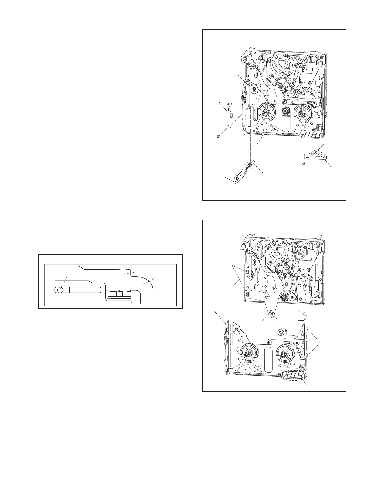
3.3.7 Mechanism adjustment
TENSION ARM
ASSY
3.3.7.1 SLIDE GUIDE PLATE adjustment
This adjustment is required when the SLIDE DECK ASSEMBLY
is removed from the MAIN DECK ASSEMBLY.
The adjustment is also required when the SLIDE GUIDE PLATE
is removed.
Refer to the Fig3-3-20Aunless otherwise instructed.
Adjustment procedure
(1) Set the PLAY mode while the HOUSING ASSEMBLY is
removed. Refer to the Fig. 3-3-8.
(2) Loosen the screw A.
(3) Press both the MAIN DECK ASSEMBLY/ SLIDE DECK
ASSEMBLY inward with an even power from both left
and right. Fully pull up the SLIDE GUIDE PLATE to the
left and tighten the screw A.
NOTE:
When pressing the SLIDE DECK ASSEMBLY, press
near the screw hole for the HOUSING ASSEMBLY attachment. Avoid pressing the sensor as it is fragile.
NOTE:
The tightening torque is 0.078N•m(0.8kgf•cm)
(4) Perform an operation check.
NOTE:
Repeat the operation check of unloading/ loading to
confirm the smooth and steady slide movement without any jam or rattle.
(1) Set the Play mode while the Housing Assembly is re-
moved. Refer to the Fig. 3-3-8.
(2) Loosen the screw B.
(3) Slide the Guide Plate up and down to set the tip of the
Tension Arm Assembly to the edge of the screw groove,
and tighten the screw B.
• The tightening torque is 0.049N•m(0.5kgf•cm)
(4) Perform an operation check.
NOTE:
Repeat loading and unloading, and make sure to
check that the top of the TENSION ARM and the edge
match properly when observed from the straight
above.
NOTE:
The adjustable range is ±0.25mm from the edge.
<NOTE>
0.5mm
EDGE
MAIN DECK ASSY
SENSOR
SLIDE
GUIDE
PLATE
Screw A
TENSION ARM
TENSION ARM
MAIN DECK ASSY
TENSION
ARM
ASSY
EDGE
( 0.25mm)
ASSY
ASSY
SENSOR
Screw B
Fig.3-3-20A
3.3.7.2 Tension Arm Assembly adjustment
This adjustment is required when the Tension Arm Assembly is
replaced.
Refer to the Fig.3-3-20Bunless otherwise instructed.
Adjustment procedure
Fig.3-3-20B
(No.YF228<Rev.001>)1-31
Page 32

3.3.8 REMARKS
3.3.8.1 Cleaning
(1) For cleaning of the upper drum (particularly video heads),
use fine-woven cotton cloth with alcohol soaks through. Do
not move the cloth but turn the upper drum counterclockwise.
NOTE:
Make sure not to move the cloth in the vertical direction
to the video head, since it may cause damage of the video
heads.
(2) For cleaning of parts of the tape transport system except
the upper drum, use fine-woven cotton cloth or cotton swab
soaked alcohol.
(3) After cleaning, confirm that the cleaned parts are complete-
ly dry before loading the deck with cassette tape.
3.3.8.2 Applying oil and grease
(1) Periodical oiling and greasing are not required but should
be done to new parts when replacing. If oil and grease on
the other parts of the other party are old and dirty, wipe
them clean and apply new oil or grease.
(2) For parts and points to apply oil and grease, refer to the
PARTS LIST.
Fig.3-3-21 specifies oil and grease to be used.
(3) When oiling, clean the objective parts with alcohol first and
apply one or two drop(s) of oil. Too much oiling causes rotary parts to slip because of oil leakage.
Classification Part No. Symbol in drawing
Grease KYODO-SH-JB AA
Oil YTU94027 BB
Grease
JVS-306U CC
specifies oil and grease to be used
Fig.3-3-21
1-32 (No.YF228<Rev.001>)
Page 33

SECTION 4
ADJUSTMENT
4.1 PREPARATION
4.1.1 Precaution
Camera system and deck system of this model are specially
adjusted by using PC.
However, if parts such as the following are replaced, an
adjustment is required. The adjustment must be performed in a
Service Center equipped with the concerned facilities.
• EEP ROM (IC1005 of MAIN board)
• OP BLOCK ASSEMBLY
• MONITOR ASSEMBLY
In the event of malfunction with electrical circuits, first find a
defective portion with the aid of proper test instruments as shown
in the following electrical adjustment procedure, and then
commence necessary repair/ replacement/adjustment.
• In observing chip TP, use IC clips, etc. to avoid any stress.
Prior to replacement of chip parts (especially IC), remove the
solder completely to prevent peeling of the pattern.
• Use a patch cord if necessary. As for a patch cord, see the
BOARD INTERCONNECTIONS.
• Since connectors are fragile, carefully handle them in
disconnecting and connecting the FPC.
4.1.2 REQUIRED TEST EQUIPMENT
• Personal computer (for Windows)
• Color TV monitor
• Oscilloscope (dual-trace type, observable 100MHz or higher
frequency). The one observable 300 MHz or higher frequency
is recommended.
• Digital voltmeter
• DC power supply or AC adapter
• Frequency counter (with threshold level adjuster)
4.1.3 Tools required for adjustment
Torque Driver
YTU94088
Chip IC Replacement Jig
PTS40844-2
INF Adjustment Lens
YTU92001B
Light box Assembly
YTU93096B
Focus Chart
YTU92001-018
INF Adjustment Lens Holder
Bit
YTU94088-003
Cleaning Cloth
KSMM-01
YTU94087
Gray Scale Chart
YTU94133A
Alignment Tape
MC-1
Tweezers
P-895
Guide Driver
YTU94148A-1
Mini Stand
YTU93108
Color Bar Chart
YTU94133C
Service Support System
YTU94057-107
PC Cable
QAM0099-002
Jig Connector Cable
YTU93082J
Charing Battery Adjuatment Jig
Communication Cable
YTU93112A
YTU93111-1
• Torque driver
Be sure to use to fastening the mechanism and exterior parts
because those parts must strictly be controlled for tightening
torque.
• Bit
This bit is slightly longer than those set in conventional torque
drivers.
• Tweezers
To be used for removing and installing parts and wires.
(No.YF228<Rev.001>)1-33
Page 34

• Chip IC replacement jig
To be used for adjustment of the camera system.
• Cleaning cloth
Recommended the Cleaning cloth to wipe down the video
heads, mechanism (tape transport system), optical lens surface.
• Guide driver
To be used to turn the guide roller to adjustment of the linarity
of playback envelope.
• INF adjustment lens
To be used for adjustment of the camera system. For the
usage of the INF adjustment lens, refer to the Service Bulletin
No. YA-SB-10035.
• INF adjustment lens holder
To be used together with the Camera stand for operating the
Videocamera in the stripped-down condition such as the status without the exterior parts or for using commodities that are
not yet conformable to the interchangeable ring. For the usage
of the INF lens holder, refer to the Service Bulletin No. YA-SB-
10035.
• Mini stand
To be used together with the INF adjustment lens holder. For
the usage of the Mini stand, refer to the Service Bulletin No.
YA-SB-10035.
• Light box assembly
To be used for adjustment of the camera system. For the
usage of the Light box assembly, refer to the Service Bulletin
No. YA-SB-10035.
• Gray scale chart
To be used for adjustment of the camera system. For the
usage of the INF adjustment lens, refer to the Service Bulletin
No. YA-SB-10035.
• Color bar chart
To be used for adjustment of the camera system. For the
usage of the INF adjustment lens, refer to the Service Bulletin
No. YA-SB-10035.
• Focus chart
To be used for adjustment of the camera system. For the
usage of the INF adjustment lens, refer to the Service Bulletin
No. YA-SB-10035.
• Alignment tape
To be used for check and adjustment of interchangeability of
the mechanism.
• Service support system
To be used for adjustment with a personal computer. Software
can be downloaded also from JS-net.
• PC cable
To be used to connect the Videocamera and a personal computer
with each other when a personal computer issued for adjustment.
• Communication cable
Connect the Communication cable between the PC cable and
Jig connector cable when performing a PC adjustment.
• Jig connector cable
Connected to JIG CONNECTOR of the main board and used
for electrical adjustment, etc.
• Charging Battery Adjustment Jig
This Jig is used for the adjustment of the camcorders that have
Main Body battery charging function.
4.2 JIG CONNECTOR CABLE CONNECTION
4.2.1 Connection procedure
Remove the COVER(JIG), and remove the COVER(ADJ).
GUIDE ROLLER (TU)
GUIDE ROLLER (SUP)
JIG CONNECTOR
CABLE
COMMUNICATION
CABLE
JIG CONNECTOR
TO AL_2.8VSYS
TO IF_RX
TO IF_TX
TO GND
BLUE
RED
WHITE
BLACK
COVER(JIG)
JIG CONNECTOR
COMMUNICATION
CABLE
Fig.4-2-2
RS232C
COM PORT
PC CABLE
TO ENV_OUT
TO HID
COVER(ADJ)
JIG CONNECTOR
CABLE
SERVICE SUPPORT SYSTEM
MENU
PERSONAL COMPUTER
OSCILLOSCOPEJIG CONNECTOR
1-34 (No.YF228<Rev.001>)
Page 35

Jig connector diagrams
ENV_OUT GND
KENTO2
IRU
ATFI
MVD
JIG CONNECTOR CABLE (YTU93082J)
MAIN CN102
612
11
10
9
8
7
KENTO
5
AL_2.8VSYS
4
IF_RXIF_TX
3
HID
2
1
GND
Fig.4-2-3
JIG CONN. BOARD
(PIN NO.)
GND
1
HID
2
GND
3
IF_RX
4
AL_2.8VSYS
5
KENTO
6
MVD
7
ATFI
8
ENV_OUT
9
IF_TX
10
IRU
11
KENTO2
12
4.3 MECHANISM COMPATIBILITY ADJUSTMENT
4.3.1 Tape pattern adjustment
NOTE:
Prior to the adjustment, remove the CASS.COVER.
(1) Play back the compatibility adjustment tape.
While triggering the HID, observe the waveform of ENV_OUT.
(2)
(3) Set the manual tracking mode (ATF OFF).
(4) Confirm that the waveform is entirely parallel and straight,
and free from remarkable level-down, through the tracking
operation.
Make the confirmation as follows if necessary.
If level-down is observed on the left hand side of the waveform,
(5)
straighten the level by turning the GUIDE ROLLER (SUP).
If level-down is observed on the right hand side of the waveform, straighten the level by turning the GUIDE ROLLER (TU).
(6) After the adjustment, try the unloading motion once, and
confirm that the waveform is flat when the tape has been
played back again.
(7) Play back the self-recording.
(8) Confirm that the waveform is flat.
Flatten the waveform.
4.4 ELECTRICAL ADJUSTMENT
Electrical adjustment is performed by using a personal computer
and software for SERVICE SUPPORT SYSTEM. Read
README.TXT file to use the software properly.
As for the connection of cables, see "4.2 JIG CONNECTOR
CABLE CONNECTION".
Misalignment of guide
roller height on the
supply side
ENV_OUT
HID
Misalignment of guide roller
height on the take-up side
Fig.4-3-1
Fig.4-3-2
(No.YF228<Rev.001>)1-35
Page 36

5.1 SERVICE NOTE(1)
SECTION 5
TROUBLE SHOOTING
3-2-12 3-2-13
aa
3-2-8 3-2-9 3-2-10A 3-2-11
3-2-4 3-2-7
3-2-3 3-2-5 3-2-6
3-2-23-2-1
3-2-18A3-2-16A 3-2-18B
3-2-15 3-2-19 3-2-203-2-17
aab
[18]
[11]
a
3-2-22
1 2 3 4 5 6
ac
3-2-21
[1] [2] [4][3] [5] [6] [9] [10] [11] [12] [13][7] [8]
1 2 3 4 5 6 7 8 9 10 11 12 13 14 15 16 17 18 19 20 21 22 23 24 25 26 27
CABINET PARTS AND ELECTRICAL PARTS(1)
Symbol No.
Removing order of screw
1-36 (No.YF228<Rev.001>)
[14] [15] [16] [17] [18] [19] [20]
28 29 30 31 32 33 34 35 36 37 38 39 40 41 42 43 44 45 46 47 48
CABINET PARTS AND ELECTRICAL PARTS(2)
Symbol No.
Place to stick screw
Screw tightening torque
Reference drawing (Fig.No.)
Removing order of screw
3-2-14
1 2 3 4 5 6 7 8 9 10 11 12 13 14
[11]OP BLOCK ASSY/CCD BOARD ASSY [18]MONITOR ASSY
Symbol No.
Place to stick screw
Screw tightening torque
Reference drawing (Fig.No.)
Removing order of screw
Place to stick screw
Screw tightening torque
Reference drawing (Fig.No.)
NOTE:
㧝)㧖and㧖㧖 (This mark shows where to attach the screws) : Do not reuse the screws because the screw lock bond was applied to prevent the screws from loosening.
Prepare the specified screws and use them in place of the removed screws.
㧞)Tightening torque for the screws
There are setting limits of the torque value for the torque driver. If the value exceeds the setting value, take it as a rough measurement (reference value),
and tighten the screw manually.
The specified torque value is a recommended value of the initial assembly. Therefore, set the value below the specified torque value in the assembling procedure.
a㧦 0.088N㨯m (0.9kgf㨯cm)ޓޓb㧦 0.078N㨯m (0.8kgf㨯cm)ޓޓc㧦 0.147N㨯m (1.5kgf㨯cm)
Be careful not to break either the screws or the screw holes.
Page 37

5.2 EMERGENCY DISPLAY
When any abnormal signal is input to the syscon CPU, an error
number is displayed on the LCD monitor. (Shown as examples
01 and 03)
In every error status, the relevant messages as shown in the examples keep appearing alternately.
Proceed with the operation following the messages.
Example (in case of the error number 01):
UNIT IN
SAFEGUARD MODE
01
REMOVE AND REATTACH
BATTERY OR DC PLUG
Example (in case of the error number 03):
01
UNIT IN
SAFEGUARD MODE
03
LCD display Emergencymode Details Possible cause
01 LOADING In the case the encoder position is not
shifted to the next point though the
loading motor has rotated in the
loading direction for 4 seconds or
more. This error is defined as [01].
02 UNLOADING In the case the encoder position is not
shifted to the next point though the
loading motor has rotated in the
unloading direction for 4 seconds or
1. The mechanism is locked during mode shift.
2. The mechanism is locked at the mechanism loading end,
because the encoder position is skipped during mechanism
mode shift.
3. No power is supplied to the loading MDA.
1. The mechanism is locked during mode shift.
2. The mechanism is locked at the mechanism loading end,
because the encoder position is skipped during mechanism
mode shift.
more. This error is defined as [02].
03 REEL FG(TU & SUP) In the case no REEL FG is produced
for seconds shown in the table below
or more in the capstan rotation mode
after loading was complete, the
mechanism mode is shifted to STOP
with the pinch roller set off. This error
is defined as [03].However, no REEL
EMG is detected in the SLW/STILL
mode.
1. The idler gear does not engage with the reel disk well.
2. Though the idler gear and reel disk are engaged with each
other, the tape is not wound because of overload to the
mechanism.
3. No FG pulse is output from the reel sensor.
4. No power is supplied to the reel sensor.
5. Tape transport operation takes place with a cassette having
no tape inside.
6. The tape slackens and no pulse is produced until the slack
is taken up and the tape comes into the normal status.
REEL(SUP) REEL(TU)
PB/REC
S-FWD
S-REW
FF
REW
04 DRUM FG In the case there is no DRUM FG
input in the drum rotation mode for 4
seconds or more. This error is defined
as [04], and the mechanism mode is
shifted to STOP with the pinch roller
set off.
3 SEC
3 SEC
0.3 SEC
3 SEC
0.1 SEC
3 SEC
0.3 SEC
3 SEC
0.1 SEC
3 SEC
1. The drum cannot be started or drum rotation is stopped
because tape transport load is too high.
1) Tape tension is extremely high.
2) The tape is damaged or soiled with grease, etc.
2. The DRUM FG signal is not received by the syscon CPU.
1) Disconnection in the middle of the signal line.
2) Failure of the DRUM FG pulse generator (hall element).
3. No drum control voltage is supplied to the MDA.
4. No power is supplied to the DRUM MDA.
05 - - -
06 CAPSTAN FG In the case no CAPSTAN FG is
produced in the capstan rotation
mode for 2 seconds or more. This
error is defined as [06], and the
mechanism mode is shifted to STOP
with the pinch roller set off.However,
no CAPSTAN EMG is detected in the
STILL/FF/REW mode.
1. The CAPSTAN FG signal is not received by the syscon
CPU.
1) Disconnection in the middle of the signal line.
2) Failure of the CAPSTAN FG pulse generator (MR
element).
2. No capstan control voltage is supplied to the MDA.
3. The capstan cannot be started or capstan rotation is
stopped because tape transport load is too high.
1) Tape tension is extremely high. (Mechanical locking)
2) The tape is damaged or soiled with grease, etc. (Tape
tangling occurs, etc.)
Fig.5-3-1
EJECT AND
REINSERT TAPE
03
(No.YF228<Rev.001>)1-37
Page 38

5.3 TAKING OUT CASSETTE TAPE
If the tape cannot be taken out due to electrical failure, take
out the tape in the following procedure.
Please note that following is a simplified method.
Removing the cabinet parts before taking out the tape is recommended for easy tape removal considering the workability and reliability.
(1) Remove the Power Unit (battery or DC code) from the set.
(2) Remove a cover (ADJ).
NOTE
For more efficient operation, loosen and move the grip
belt prior to the procedure (2).
(3) Open the CASSETTE COVER till it is completely opened
and fixed.
(4) Attach a PVC TAPE as shown in the figure.
NOTE
Be careful of cassette tape damage caused because the
CASSETTE HOUSING ASSEMBLY is moved upward at
the unloading end (EJECT mode).
(5) To set the SLIDE DECK ASSEMBLY to the unloading end,
apply DC 3V to the electrode (terminal) on the top surface
of the LOADING MOTOR ASSEMBLY that is seen through
a hole under the cover removed in the procedure (2).
NOTE
Be careful not to attach grease or a similar substance to
the surface of the cassette tape on the tape transport
system.
(6) Wind the cassette tape by directly turning the CENTER
GEAR from the backside of the SLIDE DECK ASSEMBLY
by using a sharp tool (Chip IC replacement jig).
(7) Confirm that the cassette tape is completely wound, and
then peel off the PVC TAPE from the CASSETTE HOUSING ASSEMBLY and take out the cassette tape.
NOTE
To confirm that the cassette tape is completely wound,
confirm that one REEL DISK ASSEMBLY (SUP) rotates
as you rotate the other REEL DISK ASSEMBLY (TU).
(8) Make sure that grease or a similar substance is not at-
tached to the surface of the tape taken out in the procedure
(7). Similarly, also make sure that grease or a similar substance is not attached on the MECHANISM ASSEMBLY,
especially the tape transport system.
COVER(ADJ)
CASS.COVER
TAPE
CENTER GEAR
(DC3V)
LOADING MOTOR
GRIP BELT
CASS.HOUSEING ASSY
SLIDE DECK ASSY
CHIP IC
REPLACEMENT JIG
TAPE
Fig.5-2-1
1-38 (No.YF228<Rev.001>)
Page 39

5.4 SERVICE NOTE
Use the following chart to manage mechanism parts that are removed for disassembling the mechanism.
[1]
HOUSING ASSY DRUM ASSY
3-3-11
[4]
REEL COVER ASSY
IDLER ARM ASSY T5 ARM ASSY
[5] [6]
DRUM PROTECTOR
[2]
[3]
(NEW TYPE)(OLD TYPE)
or
[7]
3-3-11 3-3-10
[8]
S1 ARM ASSY
[11] [13] [14]
SLIDE DECK ASSY PINCH ROLLER
[9]
SLIDE GUIDE PLATE GUIDE PLATE
3-3-12
TENSION ARM ASSY
[10]
ASSY
[12]
3-3-14B
REEL DISK ASSY
(SUP : WHITE)
CASSETTE
GUIDE
3-3-14A 3-3-13
Fig.5-4-1
3-3-14B
(TU : BLACK)
REEL DISK ASSY
[15] [16]
BRAKE PLATE
(No.YF228<Rev.001>)1-39
Page 40

T.C.PLATE ASSY GUIDE RAIL
[17] [20]
SLIDE
COLLAR1
ASSY
[22]
CAPSTAN MOTOR REEL PULLEY
[23]
[18]
3-3-15
[19]
DRUM ASSY
DRIVE ARM ASSY
SLIDE
COLLAR2
3-3-163-3-17
[21]
T5 CATCHER
MOTOR
[25] [27] [28]
BRACKET ASSY
WORM
WHEEL
[26]
BELT GUIDE
GEAR COVER PRESS ARM
[24]
CENTER GEAR
ASSY
[29]
[30]
3-3-18
[31]
SUB CAM ROTARY
CONNECT GEAR
MAIN CAM
[32] [33]
ENCODER
[36]
MAIN DECK ASSY
3-3-19
Fig.5-4-2
LOADING
GEAR1
[34]
GUIDE ROLLER(S) ASSY
[35]
COMPRESSION SPRING
1-40 (No.YF228<Rev.001>)
Page 41

5.5 SERVICE NOTE(2)
-
-
-
[18] [19]
13 14 15
-
-
[16] [17]
-
-
-
[12] [13] [14] [15]
-
11 12
10
[8] [9] [10] [11]
9-
[7]
-
[6]
3-3-15
-
-
-
-
-
-
---
3-3-14B
-
-
-
-
-
-
-
--
--
-
-
-
-
-
3-3-13
-
-
--
-
ab
-
-
-
aaba/c
2120 22 23 24
[3][2] [4] [5]
[1]
12345678-
b
a
3-3-10
Symbol No.
Place to stick screw
3-3-11 3-3-12
Removing order of screw
Screw tightening torque
Reference drawing (Fig.No.)
-
-
-
-
-
3-3-16 3-3-17 3-3-18 3-3-19
bb
[20] [22] [23] [24] [25] [26] [27] [28] [29] [30] [31] [32] [33] [34] [35] [36][21]
16 17 18 19
a
Symbol No.
Place to stick screw
Removing order of screw
Fig.5-5-1
Screw tightening torque
Reference drawing (Fig.No.)
NOTE:
Pay careful attention to tightening torque for each screw.
Torque setting value of torque driver is limited. At the values over the maximum torque setting value,
fasten a screw manually not to damage the screw thread.
ޓa㧦 0.049N㨯m (0.5kgf㨯cm)ޓޓb㧦 0.039N㨯m (0.4kgf㨯cm)ޓޓc㧦 0.078N㨯m (0.8kgf㨯cm)
The tightening torque of the No.10 screw is 0.049N㨯m(0.5kgf㨯cm) for mounting, and 0.078N㨯m(0.8kgf㨯cm) for adjustment.
For details, refer to the adjustment item "2.1.6.1 Adjustment of the SLIDE GUIDE PLATE"
(No.YF228<Rev.001>)1-41
Page 42

Victor Company of Japan, Limited
Camcorder Category 12, 3-chome, Moriya-cho, Kanagawa-ku, Yokohama-city, Kanagawa-prefecture, 221-8528, Japan
(No.YF228<Rev.001>)
Printed in Japan
VPT
Page 43

SCHEMATIC DAIGRAMS
DIGITAL VIDEO CAMERA
YF228SCH<Rev.001>20082SCHEMATIC DIAGRAMSEverio
GR-D850UC, GR-D850US,
GR-D870UC, GR-D870US,
GR-D875US
CD-ROM No.SML200802
GR-D850UCM,GR-D850USM [M8D523]
GR-D870UCM,GR-D870USM
GR-D875USM [M8D525]
Lead free solder used in the board (material : Sn-Ag-Cu, melting point : 219 Centigrade)
COPYRIGHT© 2008 Victor Company of Japan, Limited
No.YF228SCH<Rev.001>
2008/2
Page 44

CHARTS AND DIAGRAMS
NOTES OF SCHEMATIC DIAGRAM
Safety precautions
The Components indentified by the symbol are
critical for safety. For continued safety, replace safety
critical components only with manufacturer's recommended parts.
1. Units of components on the schematic diagram
Unless otherwise specified.
1) All resistance values are in ohm. 1/6 W, 1/8 W (refer to
parts list).
Chip resistors are 1/16 W.
K: KΩ(1000Ω), M: MΩ (1000KΩ)
2) All capacitance values are in µF, (P: PF).
3) All inductance values are in µH, (m: mH).
4) All diodes are 1SS133, MA165 or 1N4148M (refer to parts
list).
Note: The Parts Number, value and rated voltage etc. in
the Schematic Diagram are for references only.
When replacing the parts, refer to the Parts List.
2. Indications of control voltage
AUX : Active at high.
AUX or AUX(L) : Active at low.
!
4. Voltage measurement
1) Regulator (DC/DC CONV) circuits
REC : Colour bar signal.
PB : Alignment tape (Colour bar).
— : Unmeasurable or unnecessary to measure.
2) Indication on schematic diagram
Voltage indications for REC and PB mode on the schematic diagram are as shown below.
REC mode
12 3
2.5
(5.0)
PB mode
1.8
PB and REC modes
(Voltage of PB and REC modes
are the same)
Note: If the voltages are not indicated on the schematic
diagram, refer to the voltage charts.
5. Signal path Symbols
The arrows indicate the signal path as follows.
NOTE : The arrow is DVC unique object.
Playback signal path
Playback and recording signal path
CIRCUIT BOARD NOTES
1. Foil and Component sides
1) Foil side (B side) :
Parts on the foil side seen from foil face (pattern face)
are indicated.
2) Component side (A side) :
Parts on the component side seen from component face
(parts face) indicated.
rts location are indicated by guide scale on the circuit board.
2. Parts location guides
Parts location are indicated by guide scale on the circuit board.
REF No.
IC101 B C 6 A
(A : Component side)
D : Discrete component)
B : Foil side
C : Chip component
Note: For general information in service manual, please
refer to the Service Manual of GENERAL INFORMATION Edition 4 No. 82054D (January 1994).
LOCATION
IC
Category : IC
Horizontal “A” zone
Vertical “6” zone
3. Interpreting Connector indications
1
2
Removable connector
3
1
2
Wire soldered directly on board
3
1
Non-removable Board connector
2
3
1
2
4
Board to Board
3
Connected pattern on board
The arrows indicate signal path
Note: For the destination of each signal and further line
connections that are cut off from the diagram,
refer to "BOARD INTERCONNECTIONS"
Recording signal path
(including E-E signal path)
Capstan servo path
Drum servo path
(Example)
R-Y
Playback R-Y signal path
Y
Recording Y signal path
6. Indication of the parts for adjustments
The parts for the adjustments are surrounded with the circle
as shown below.
7. Indication of the parts not mounted on the circuit board
“OPEN” is indicated by the parts not mounted on the circuit
board.
R216
OPEN
(No.YF228<Rev.001>)2-1 2-2(No.YF228<Rev.001>)
Page 45

BOARD INTERCONNECTION
OP BLOCK
(K241)
<FPC-M1-501C>
YTU94074-25
YTU94077-25
CN4901
MAIN
10
MAIN IF
(Page2-5)
F_PTR_AD76F_VCC5
ZOOM014
ZOOM043
ZOOM032
ZOOM021
HGVCC+
OPDRV_CS
OP_CLK
DUMP+10
GND9
OP_THRMO8
HGVSS-
HGOUT-
HGOUT+
(Page2-19)
OPDRV_PS
OP_OUT
OP_IN
DRIVE+13
HGOUT+12
HGVCC+11
Z_LED
DRIVE-
DRIVE+
ZOOM01
OP DRV
VD_FZ
OP_RST
DRIVE-14
HGVSS-15
ZOOM04
HGOUT-16
ZOOM03
ZOOM02
OPDRV_VD
GND18
DUMP-17
F_VCC
CLK27OP
VDMDA
FOCUS0219
FOCUS02
FOCUSO4
H_GAIN
FOCUS0421
FOCUS0320
FOCUS03
REG_4.65V
M_REG4.65
H_OFFSET
DUMP-
FOCUS01
REG_2.8V
WB_SENS
GND
Z_LED2423FOCUS0122
DUMP+
<FPC-M1-507>
YTU94074-20
YTU94077-20
YTU94074-16
V41
V32
V23
V14
GND5
GND6
VOUT7
CCD
20
YTU94077-16
YTU94074-18
YTU94077-18
(Page2-26)
VL 11
H2 13
H1 12
RG 9
SUB 10
VDD 8
Z_PTR_AD25
TEST 14
2019181716151413121110
CCD_-7.5V20
CN4201
GND19
H118
GND17
H216
SUB15
RG14
GND13
V412
V311
V210
V1
REG_12V
CDSTG_RST
CDSTG_CS
CAM_CLK
CAM_OUT
VDIN
ADIN0
CLKI
HDIN
CN5001
987654321
V19
GND8
GND7
CCD_OUT6
GND5
GND4
GND3
REG_12V2
REG_12V1
V4
V2
V3
H2
H1
RG
SUB
CCD_-7.5V
CDS/TG MDA
(Page2-17) (Page2-9)
ADIN1
ADIN7
ADIN2
ADIN3
ADIN4
ADIN5
ADIN6
ADIN8
CCD_OUT
REG_-7.5V
REG_2.8V
ADIN10
ADIN9
REG_12V
ADIN11
CN1604
GND
Z32 Mecha
GND15
S_SENS16
MIC313
MECHA_VCC
14
SENSOR CAPSTAN MOTOR DRUM MOTOR HEAD L.MOTOR/R.ENC
C_FG-2
C_FG+3
GND4
C_COIL_V5
C_COIL_V6
HG_W-7
HG_V-8
HG_U-9
HG_BS+10
HG_BS-11
C_COIL_W12
C_COIL_W13
HG_U+14
HG_V+15
HG_W+16
C_COIL_U17
C_COIL_U18
CAS_SW1
TAPE_LED2
GND3
T_RL+4
T_RL-5
S_RL-6
REEL_VCC7
S_RL+8
E_SENS9
MIC110
MIC211
REC_SAFE12
T_RL-
S_RL-
S_RL+
T_REEL
T_RL+
S_REEL
MDA_PS
HG_BS-
L_FRB
HG_BS+
LD_ON
HG_V-
HG_W-
CAP_REF
CAP_FG
HG_U-
C_FRB
HG_V+
HG_W+
DRUM_REF
DRUM_FG
HG_U+
C_COIL_U
DRUM_PG
C_COIL_V
C_COIL_W
C_FG-
C_FG+
MECHA_VCC
D_COIL_V
CAP_PWR
M_UNREG
D_COIL_U
D_COIL_W
DRUM_PWR
CAP_ERR
D_PFG+
COIL_COM
DRUM_ERR
D_FG-
D_PG-
LOAD_FWD
LOAD_REV
M_REG4.65
REG_2.8V
MECHA_VCC
1
GND
D_FG-10
D_PFG+11
YTU94074-11
YTU94077-11
D_COIL_V6
D_COIL_V7
D_COIL_U8
D_COIL_U9
D_COIL_W4
D_COIL_W5
ENV_OUT
D_PG-2
COIL_COM3
ATFI
GND1
(Page2-15)
REC_DATA
VRB_ATF
REC_CLK
YTU94074-8
YTU94077-8
1S6
1F7
GND8
1F
1S
PRE/REC
REC_ADJ
REC_CTL
VRB_AGC
VREF_1.1
AGC_OUT
GND4
GND5
2F
ATF_GAIN
AGC_CTL
YTU94074-8
YTU94077-8
FRONT
60
(Page2-33)
W/B Sensor
IR Sensor LED LIGHT
CN801
YTU94074-8
YTU94077-8
8
GND2
GND1
CAM_SW_C2
CAM_SW_B3
CAM_SW_A4
DEW_SENS5
LOAD_FWD6
LOAD_REV7
GND8
GND1
2S2
2F3
GND1
1234567
REMOTE8
REG_2.8V7
WB_SENS6
REG_4.65V5
REG_4.65V4
LAMP_ONH3
<FPC-06-WR1>
CN108CN1602 CN1601CN3501CN1603
YTU94074-12
YTU94077-12
2S
REG_4.65V
REG_2.8V
GND
HID
PBH
RECH
REG_12V
REG_2.8V
GND
MONI
(Page2-25)
BGR
LCD_G
LCD_R
LCD_B
L.CASE(P)UNIT
(Page2-34)
CN105
PHOTO_F1
GND2
ZOOM_SW3
REG_2.8V4
GND5
AL_2.8V6
PWR_LED7
GND8
TRIG_SW9
DIAL_REC10
DIAL_OFF11
DIAL_PB12
WT
REC
OFF
PLAY
AIDAT
AIBCK
AIMCK
AODAT
AILRCK
AUDIO
(Page2-11)
INT_L
INT_GND
SPK+
INT_R
S_SHUT
SPK-
AU_LV_CLK
AUDIO_CS
AU_LV_OUT
BUZZER
REG_4.65V
REG_2.8V
GND
AU_SIG/L
AU_SIG/R
L_MUTE
PD_L
A_MUTE
INT MIC
1
INT/R
INT_GND 2
INT_GND 3
INT/L
4
CN2601
7
8
<FPC-M1-313>
YTU94074-28
YTU94077-28
CN103
CN7002
REG_8.5V 1
REG_4.65V 2
50
BLUE3
RGT2
TEST21
LED_12V 3
LCD_STV 6
LCD_ENB
REG_2.8V 4
LCD_PSIG 5
LCD_CKV1
MONITOR
(Page2-31)
NRW9
HCK28
HCK17
PSIG6
GREEN5
RED4
LCD_DSG 11
LCD_DWN 9
LCD_XDSG_CPU 10
HST12
REF11
TEST110
CN7001
YTU94074-24
YTU94077-24
NOTES: The number of patch cords ( ) are indicated by interconnected.
( ) indicates the block No. and symbol No. of the WIRE or the FPC.
LCD(MONITOR) MODULE
<FPC or WIRE - 03 -WR1>
Block No.
LCD_STH 12
LCD_COM 13
XSTBY14
PCG13
Symbol No.
17
15
19
18
B
R
G
GND 21
KEY_A
KEY_C 16
M_RVS 14
Hall
device
VSS17
NC16
VSSG15
LCD_CKH1 22
LED_PWM/LCD_CTL 20
10111213141516171819202122232425262728
COM24
CS23
VST22
VCK21
EN20
DWN19
VDO18
GND 29
GND 28
GND 27
GND 26
GND 25
USB_DN 30
LCD_RGT 24
LCD_CKH2 23
123456789
GND 33
V_BUS 31
USB_DP 32
40
MONITOR SW
DSC VIDEO
GND 38
TPB- 37
TPA- 34
TPB+ 36
TPA+ 35
JACK
(Page2-29)
USB
2
1
VBUS
DEV_D-
PSCTL_YC 39
3
DEV_D+
REG_2.8V 41
REG_4.65V 40
101112131415161718192021222324
5ID4
GND
CLKI
CLK27OP
OPDRV_VD
H_OFFSET
H_GAIN
VDMDA
AIBCK
AIMCK
AILRCK
AODAT
AIDAT
S_SHUT
Y_IN
Y_IN 43
C_IN 45
S_DET 44
WIDE_CTL 42
TPA+
TPA-
TPB+
TPB-
7
6
F_GND
F_GND
<FPC-M1-313>
YTU94074-24
YTU94077-24
CN101
SD_WP1
MMC_DOUT2
MMC_CD3
MMC_CLK4
MMC_DIN5
MMC_CS6
DSC_3.1V7
DSC_3.1V8
P_GND9
P_GND10
P_GND11
S_GND12
S_GND13
SPK_-14
SPK_+15
P_GND16
P_GND17
P_GND18
P_GND19
P_GND20
EJT_SW21
D_BATT22
T_BATT23
BATT+24
BATT+25
BATT+26
BATT+27
BATT+28
BATT_CHK29
ADP_DC30
ADP_DC31
ADP_DC32
ADP_DC33
ADP_DC34
ADP_L35
LITHIUM36
V_OUT37
P_DET38
AU_SIG/R39
AU_SIG/L40
CN501
1
2
3
4
5
6
7
8
9
10
11
12
13
14
15
16
17
18
19
20
21
22
23
24
25
26
27
28
29
30
31
32
33
34
35
36
37
38
39
40
SPEAKER
<FPC-03-WR1>
YTU94105-40
YTU94077-40
BATTERY TERMINAL
CN504
1
2
3
4
30
5
(Page2-27)
6
7
8
9
10
MMC_CS1
SD_DATA29
11
12
13
14
15
16
17
18
19
20
21
22
23
24
25
26
27
28
29
30
31
32
SPK-2
SPK+1
REAR
VSS(GND)3
Dat2MMC2
CN503
SD
EJECT SW
LITHIUM
CN502
-CT+
DC
AV
SD_DATA18
Dat2Host7
VSS2/CD6
MMC_CLK5
VDD(DSC_3V)4
SD_WP12
VSS(GND)11
CARD_DET10
13
GND
14
GND
CAS_SW
REC_SAFE
EJT_SW
D_BATT
S_REEL
P_DET
T_REEL
V_BUS
USB_DN
USB_DP
DSC_CLKW
DSY[O0-O7]
DSC[O0-O7]
DSYI[O0-O7]
DSCI[O0-O7]
DSC_HDW
(DSC MODEL ONLY)
DSC_FLDW
DSC_VDW
DSCCLK27
CLK48
L_FRB
C_FRB
LD_ON
CAP_FG
MDA_PS
CAP_REF
D_GAIN
I_MTR
SYS_RSTL
LIT_2.8V
CHRG_EVR
USBIN_L
USBDOWN
DRUM_FG
DRUM_PG
DRUM_REF
REG_ID_CLK
REG_ID_OUT
REG_CS
FLSH_RST
RESET
TDI_DSC
TCK_DSC
TDO_DSC
TMS_DSC
TRST_DSC
DSC
(Page2-23)
DSC_RST
DSC_DT_OUT
DSC_CS
DSC_DT_IN
DSC_CLK
DEW_SENS
CAM_SW_B
CAM_SW_A
CAM_SW_C
MMC_CD
USBIN_L
DSC_WKUP
CAPT_REG
DSC_STS
MXDT_OUT
DSC_CS
DSC_DT_IN
DSC_DT_OUT
DSC_CLK
DSC_RST
FLSH_RST
USBDOWN
HID
PBH
RECH
OCD_SCL
OCD_SDA
REMOTE
LAMP_ONH
AL_2.8V
REG_2.8V
GND
V_BATT
BAT_H
RXD2
EMU1
MXDT_OUT
DSC_STS
TXD2
DSC_DBG
CAPT_REG
DSC_WKUP
DSC_3.1V
REG_1.8V
MMC_CS
MMC_DIN
MMC_CLK
MMC_CD
MMC_DOUT
SD_WP
GND
REG_1.2V
REG_4.65V
M_REG4.65
(Page2-21)
V_BATT
BAT_H
REG_ID_OUT
REG_CS
DSC_3.1V
REG_2.8V
REG
REG_ID_CLK
CHRG_EVR
REG_8.5V
REG_1.8V
LIT_2.8V
REG_12V
I_MTR
SYS_RSTL
AL_2.8V
REG_-7.5V
D_GAIN
M_UNREG
CAP_PWR
CAP_ERR
DRUM_PWR
DRUM_ERR
ADP_DC
BATT_CHK
T_BATT
BATT_+
LITHIUM
GND
<FPC-03-WR1>
CN106
1
2
3
4
5
6
7
8
9
10
11
12
13
14
15
16
17
18
19
20
21
22
23
24
25
26
27
28
29
30
31
32
VDIN
HDIN
ADIN8
ADIN9
ADIN11
ADIN10
WIDE_CTL
C_IN
TPB-
TPA-
TPA+
TPB+
48
GND 46
KEY_C 47
P_MEDIA
MONI_SW 50
DATA_SW 49
CN401
123456789
ADIN7
ADIN6
ADIN5
ADIN4
ADIN3
ADIN2
ADIN1
ADIN0
OMT0
MFLD
REC_ADJ
AGC_CTL
ATF_GAIN
PSCTL
AEBEND
MVD
CDSTG_CS
CDSTG_RST
CAM_OUT
CAM_CLK
OP_THRMO
Z_PTR_AD
F_PTR_AD
OP_CLK
OPDRV_CS
OP_OUT
OP_IN
OPDRV_PS
OP_RST
VD_FZ
A_MUTE
L_MUTE
PD_L
BUZZER
AUDIO_CS
AU_LV_CLK
AU_LV_OUT
DV
ATFI
VRB_ATF
REC_CTL
VREF_1.1
VRB_AGC
AGC_OUT
REC_DATA
PARAGON 4
(Page2-13)
XINT
DSP_RST
TSR
HID
FRP
SPA
AFBEND
KEY_A
DATA_SW
MONI_SW
REC_CLK
TV_SEL
KEY_C
CDAS
M_RVS
DSP_CS
VDIN
LCD_CTL
LED_12V
CDRE
LCD_RGT
LED_PWM
CPU_WAIT
CDWE
P_MEDIA
LCD_COM
LCD_PSIG
LCD_XDSC
ADDT[00-15]
TSR
FRP
S_DET
LCD_DWN
LCD_XDSG_CPU
LCD_ENB
LCD_DSG
SPA
PSCTL
PSCTL_YC
LCD_STV
DSP_CS
LCD_STH
LCD_CKV1
XINT
DSP_RST
EXTRG0
LCD_CKH2
LCD_CKH1
MVD
MFLD
SYS_RSTL
KENTO
OMT0
KENTO2
IF_RX
TV_SEL
IF_TX
LCD_B
LCD_R
LCD_G
DSCCLK27
DSC_VDW
DSC_FLDW
DSC_HDW
DSCI[O0-O7]
DSYI[O0-O7]
DSC[O0-O7]
DSY[O0-O7]
DSC_CLKW
REG_1.2V
DSC_3.1V
REG_2.8V
REG_4.65V
V_OUT
CDAS
AFBEND
AEBEND
CPU_WAIT
CPU
(Page2-7)
AL_2.8VSYS
PHOTO_F
IRU
CLK48
LED_12V
GND
CDRE
CDWE
ZOOM_SW
ADDT[00-15]
DIAL_REC
PWR_LED
E_SENS
S_SENS
DIAL_OFF
DIAL_PB
TAPE_LED
TRIG_SW
MIC3
REEL_VCC
MIC1
MIC2
ADP_L
T_BATT
S
2
CN104 CN102
15
16
17
18
TDI
TCK
TMS
TRST
9
10
11
12
13
14
TDO
TXD2
EMU1
RESET
DSC_3.1V
DSC_DBG
7
8
RXD2
AL_2.8VSYS
6
NRST
5
EXTRG0
3
4
OCD_SCL
OCD_SDA
2
GND1GND
NC
4
IRU 11
KENTO 6
KENTO2 12
AL_2.8VSYS 5
HID
ATFI 8
GND 3
IF_TX 10
IF_RX
ENV_OUT 9
JIG CONNECTOR
MVD 7
GND 1
yf228_y10710001a_rev0.2
(No.YF228<Rev.001>)2-3 2-4(No.YF228<Rev.001>)
Page 46

MAIN(MAIN IF) SCHEMATIC DIAGRAM
To CPU
To OP DRV
To CPU
REMOTE
REG_2.8V
WB_SENS
REG_4.65V
REG_4.65V
LAMP_ONH
To OP DRV
To MDA
To MAIN IF
(CN1603),
MDA
To CPU
To CPU
MIC2
REC_SAFE
GNDBMECHA_VCC
MIC3
S_SENS
CN1604
QGF0543F3-16X
BOTTOM CONTACT NON-ZIF
To FROMT (CN801)
CN108
QGF0543F3-08X
BOTTOM CONTACT NON-ZIF
8
7
6
5
4
3
GND
2
GND
1
To CAPSTAN MOTOR To DRUM MOTOR
CN1603
QGF0543F3-18X
TOP CONTACT NON ZIF
To MIC
CN2601
QGA1001F1-04X
INT_R
1
INT/R
INT_GND 2
INT_GND 3
INT/L
INT_GND
To AUDIO
INT_GND
4
INT_L
To MDA
To CPU
E_SENS
MIC1
S_RL+
T_RL-
S_RL-
T_RL+
REEL_VCC
10111213141516
To PRE/REC
To PRE/REC
GND
GND
GND
1S
2F
2S
1F
1
To MDA
HG_U+
C_COIL_W
HG_BS-
HG_V+
C_COIL_U
HG_W+
C_COIL_W
C_COIL_U
181716151413121110
To CPU
CAS_SW
TAPE_LED
GND
123456789
To HEAD
GND
CN3501
QGF0543F3-08X
TOP CONTACT NON-ZIF
8765432
C_COIL_V
HG_BS+
C_COIL_V
HG_U-
HG_V-
HG_W-
987654321
GND
ZOOM02
CN4901
QGF0543F3-25X
BOTTOM CONTACT NON-ZIF
To MAIN IF
(CN1604),
MDA
C_FG+
MECHA_VCC
C_FG-
ZOOM03
To CPU
ZOOM01
ZOOM04
F_PTR_AD
F_VCC
To MDA
LOAD_REV
DEW_SENS
LOAD_FWD
GND
8765432
CN1602
QGF0543F3-11X
TOP CONTACT NON ZIF
D_PFG+
D_COIL_U
D_COIL_U
D_FG-
987654321
11
10
OP_THRMO
GND
DUMP+
987654321
10
To CPU
CAM_SW_B
CAM_SW_A
To MDA
D_COIL_V
D_COIL_V
HGVCC+
HGOUT+
GND
GND
CAM_SW_C
1
D_COIL_W
D_COIL_W
To CPU
To OP DRV
GND
HGVSS-
DRIVE-
DRIVE+
HGOUT-
TL102 TL103
**
To LOADING MOTOR
AND ROTARY ENCODER
CN1601
QGF0543F3-08X
TOP CONTACT NON ZIF
GND
COIL_COM
D_PG-
To PARAGON4
DUMP-
FOCUS03
FOCUS02
To OP DRV
FOCUS04
FOCUS01
Z_PTR_AD
Z_LED
252423222120191817161514131211
To CPU
TDI_DSC
TRST_DSC
TDI 17
TRST 18
TCK_DSC
TMS_DSC
TCK 15
TMS 16
RESET
TDO_DSC
TDO 14
RESET 13
EMU1
EMU1 12
DSC_3.1V
DSC_DBG
DSC_3.1V 11
DSC_DBG 10
NOT USED
TXD2
AL_2.8VSYS
RXD2
7
TXD2 9
RXD2 8
AL_2.8VSYS
REG_12V
REG_12V
To CCD (CN5001)To OP BLOCK(K241)To SENSOR
CN4201
QGF0565C1-20W
VERTICAL NON ZIF
OCD_SCL
EXTRG0
GND
OCD_SDA
SYS_RSTL
GND 2
NRST 6
EXTRG0 5
OCD_SCL 3
OCD_SDA 4
GND
GND
GND
NOT USED
CN104
QGF0543F3-18X
BOTTOM CONTACT NON ZIF
GND 1
To CDS/TG
GND
CCD_OUT
V1
GND
GND
987654321
To CPU
To CPU
ZOOM_SW
GND
PHOTO_F
REG_2.8V
To L.CASE(P) UNIT
CN105
QGF0534F3-12X
VERTICAL CONTACT NON ZIF
V2
V3
V4
To CPU,REG
AL_2.8V
PWR_LED
GND
GND
GND
SUB
To CPU
DIAL_REC
TRIG_SW
987654321
MECHA SIDE
GND
H2
DIAL_PB
DIAL_OFF
121110
CCD_-7.5V
H1
GND
2019181716151413121110
MAIN(MAIN IF)
10
To REAR(CN501)
#
CN101
QGF0534F2-40X
BOTTOM CONTACT ONE TOUCH
SD_WP1
MMC_DOUT2
MMC_CD3
MMC_CLK4
MMC_DIN5
MMC_CS6
DSC_3.1V7
DSC_3.1V8
P_GND9
P_GND10
P_GND11
S_GND12
S_GND13
SPK_-14
SPK_+
15
P_GND
16
P_GND17
P_GND18
P_GND19
20
P_GND
EJT_SW
21
D_BATT
22
T_BATT23
BATT+
24
BATT+25
BATT+26
BATT+
27
BATT+
28
BATT_CHK
29
ADP_DC
30
ADP_DC
31
ADP_DC
32
ADP_DC33
ADP_DC
34
ADP_L
35
LITHIUM
36
V_OUT37
P_DET
38
AU_SIG/R39
AU_SIG/L
40
To REAR(CN504)
#
CN106
QGF0534F2-32X
P_GND1
P_GND2
P_GND3
S_GND4
S_GND5
SPK_-6
SPK_+7
P_GND8
P_GND9
P_GND10
P_GND11
P_GND12
EJT_SW13
D_BATT14
T_BATT15
BATT+16
BATT+17
BATT+18
BATT+19
BATT+20
BATT_CHK21
ADP_DC22
ADP_DC23
ADP_DC24
ADP_DC25
ADP_DC26
ADP_L27
LITHIUM28
V_OUT29
P_DET30
AU_SIG/R31
AU_SIG/L32
To CPU
To REG
D_BATT
T_BATT
BATT_+
C104
MMC_DOUT
MMC_CD
MMC_CLK
MMC_DIN
MMC_CS
DSC_3.1V
SPK+
EJT_SW
BATT_CHK
ADP_DC
SD_WP
SPK-
To DSC
To CPU,DSC
To DSC
GND
To AUDIO
To CPU
C102
1
*
*
3
2
C103
D101
*
*
To REG
To CPU
To REG
To PARAGON4
To CPU
To AUDIO
ADP_L
LITHIUM
V_OUT
P_DET
AU_SIG/R
AU_SIG/L
To PARAGON4
LCD_STV
LCD_CKV1
LCD_ENB
To PARAGON4
LED_12V
*
LCD_PSIG
REG_2.8V
REG_4.65V
R103
To REG
REG_8.5V
CN103
QGF0566C1-50X
VERTICAL ONE TOUCH
LCD_XDSG_CPU
To CPU
To PARAGON4
LED_PWM
LCD_CTL
To CPU
To PARAGON4
WIDE_CTL
S_DET
Y_IN
REG_2.8V
REG_4.65V
To CPU
GND
PSCTL_YC
To CPU
To PARAGON4
MONI_SW
DATA_SW
P_MEDIA
KEY_C
GND
C_IN
5049484746454443424140393837363534333231302928272625242322212019181716151413121110
To JACK (CN401)
To PARAGON4
TPB+
TPA-
TPA+RGTPB-
GND
USB_DP
To DSC
USB_DN
V_BUS
GND
To CPU
LCD_RGT
To PARAGON4
R101
GND
LCD_CKH2
LCD_CKH1
*
To MONI
KEY_A
To CPU
To PARAGON4
KEY_C
M_RVS
G
R
LCD_STH
LCD_COM
LCD_DSG
To CPUTo CPU
LCD_XDSG
*
R106
To CPU
LCD_DWN
987654321
To MONITOR (CN7002)
NOTES: 1. For the destination of each signal and further line connections that are cut off from this diagram, refer to "BOARD INTERCONNECTIONS".
2. The parts with marked ( ) is not used.
(No.YF228<Rev.001>)2-5 2-6(No.YF228<Rev.001>)
#:Different Parts
CN101
To CPU
To PRE/REC
To CPU,PARAGON4
To PARAGON4,PRE/REC
To CPU,PARAGON4,PRE/REC
ATFI
AL_2.8VSYS
KENTO
IF_RX
IF_TX
KENTO2
IRU
4938271
12611510
NO
YESCN106
DSCNon DSC
YES
NO
GND
ENV_OUT
GND
MVD
HID
To JIG CONNECTOR
CN102
QGB0801K2-12X
BOARD TO BOARD CONNECTOR
yf228_y10705001a_rev0.2
Page 47

MAIN(CPU) SCHEMATIC DIAGRAM
MAIN(CPU)
RA1003
100K
Q1006
2SC4617/QR/-X
R1045
4.7K
R1051 0Ω
R1052 8.2K
R1046
10K
10
876
123
R1053
47K
R1086 100K
5
4
R1036 560
R1047
OPEN
C1047
10K
10K
R1077
R1078
C1051 0.022
C1052 0.022
0.022
C1054
C1053
0.022
OPEN
R1039
OPEN
R1050
180k
Q1007
DTC124EE-X
R1054
39K
RA1004
100K
C1048
OPEN
1
2
3
4
R1048 2.7K
876
123
To MAIN IF(CN105),REG
To MAIN IF(CN102)
To MAIN IF(CN101,CN106)
To MAIN IF(CN101,CN106)
To MAIN IF(CN101,CN106)
To MAIN IF(CN101,CN106),REG
To MAIN IF(CN108)
To MAIN IF(CN105)
JIG CONNECTOR T2R
To MAIN IF(CN102)
JIG CONNECTOR FLASH
To MAIN IF(CN4901)
To MAIN IF(CN101,CN106)
To MAIN IF(CN103)
To MAIN IF(CN101,CN106)
To MAIN IF(CN1604)
To MAIN IF(CN103)
To MAIN IF(CN105)
To MAIN IF(CN103)
To MAIN IF(CN105)
To MAIN IF(CN103)
To REG
To DSC
To DSC
To REG
To DSC
To REG
FRONT UNIT
To DSC
To REG
To AUDIO
To DSC
To MDA
REG
REG
REAR UNIT
REAR UNIT
AUDIO
TO DSC
OPE
AL_2.8VSYS
MXDT_OUT
USBDOWN
CAPT_REQ
FLSH_RST
DSC_WKUP
DSC_DT_IN
DSC_DT_OUT
CHRG_EVR
REG_ID_CLK
REG_ID_OUT
SYS_RSTL
LAMP_ONH
AUDIO_CS
AU_LV_CLK
AU_LV_OUT
OP
OP_THRMO
ZOOM_SW
LCD_XDSG_CPU
LCD_DWN
DRUM_PG
DRUM_FG
DRUM_REF
AL_2.8V
LIT_2.8V
REG_2.8V
MMC_CD
DSC_STS
DSC_RST
BAT_H
DSC_CS
DSC_CLK
D_BATT
V_BATT
I_MTR
D_GAIN
REG_CS
ADP_L
T_BATT
REMOTE
DIAL_REC
DIAL_OFF
DIAL_PB
TRIG_SW
PWR_LED
KENTO
KENTO2
EXTRG0
OCD_SCL
OCD_SDA
SYS_RSTL
A_MUTE
L_MUTE
BUZZER
USBIN_L
Z_PTR_AD
F_PTR_AD
P_DET
S_DET
EJT_SW
CAS_SW
MONI_SW
PHOTO_F
DATA_SW
KEY_A
KEY_C
M_RVS
LCD_CTL
LCD_RGT
P_MEDIA
MDA
T_REEL
S_REEL
LD_ON
MDA_PS
C_FRB
L_FRB
CAP_FG
CAP_REF
GND
IF_RX
PD_L
IRU
IF_TX
Q1005
DTC143XE-X
R1037
OPEN
R1049
68k
C1055 1
5
4
8
7
6
5
AL_2.8VSYS
3
1
RA1002
100K
RA1009
3.3K
1
2
3
4
R1056
22K
876
123
D1001
DA221-X
2
C1050
OPEN
8
7
6
5
MXDT_OUT
MMC_CD
USBDOWN
DSC_STS
CAPT_REQ
FLSH_RST
DSC_WKUP
DSC_RST
BAT_H
DSC_CS
DSC_DT_IN
DSC_CLK
DSC_DT_OUT
D_BATT
V_BATT
I_MTR
D_GAIN
CHRG_EVR
REG_CS
REG_ID_CLK
REG_ID_OUT
SYS_RSTL
ADP_L
T_BATT
REMOTE
LAMP_ONH
DIAL_REC
DIAL_OFF
DIAL_PB
TRIG_SW
CHRG_LON
REMOTE
KENTO
KENTO2
EXTRG0
OCD_SCL
OCD_SDA
SYS_RSTL
A_MUTE
L_MUTE
AUDIO_CS
AU_LV_CLK
AU_LV_OUT
PD_L
BZ_ENV
BZ_FREQ
OP_THRMO
Z_PTR_LV
F_PTR_LV
5
4
P_DET
S_DET
EJT_SW
CAS_SW
MONI_SW
PHOTO_F
DATA_SW
KEY_A
KEY_C
M_RVS
ZOOM_SW
LCD_XDSG_CPU
LCD_CTL
LCD_RGT
LCD_DWN
P_MEDIA
T_REEL
S_REEL
LD_ON
MDA_PS
C_FRB
C_FRB2
RA1006
10K
L_FRB2
L_FRB
CAP_FG
DRUM_PG
DRUM_FG
CAP_PWM
DRUM_PWM
EXTRG0
L1002
REG_2.8V
L1001
C1014
OPEN
C1009
OPEN
C1013
0.01
C1008
10
C1004
22/6.3
REG_2.8V
AL_2.8V
10µ
10µ
R1095
100K
AL_2.8V
AL_2.8VSYS
R1009
TL1021
TL1029
TL1027
TL1030
TL1028
TL1026
TL1031
1K
TL1063
IC1006
S-35190A-G-X
5
6
SCK
7
XOUT
SIO
8
VDD
33
VD_FZ
112
NC
CAP_FG
150
DRUM_FG
8
NC
108
NC
177
L_MUTE
74
A_MUTE
143
NC
173
XINT
105
JLIP_INT
134
BAT_H
230
DSC_CS
24
OMT0
36
NC
103
MFLD
109
P_MEDIA
194
NC
18
CHRG_EVR
159
CAP_PWM
93
DRUM_PWM
92
EEP_CLK
97
EEP_OUT
162
EEP_IN
23
LCD_XDSG_CPU
245
TXD
101
RXD
166
AU_LV_CLK
132
AU_LV_OUT
62
AUDIO_CS
144
MIC_SCL
52
MIC_SDA
122
MIC_CTL
123
NC
192
GND
233
GND
206
NC
83
MXDT_OUT
79
MMC_L
4
USBDOWN
78
DSC_STS
147
CAPT_REQ
146
FLSH_RST
149
DSC_WKUP
5
DSC_RST
80
NC
127
EEP_CS
219
REG_CS
28
NC
126
NC
125
USBIN_L
55
RTC_CS
246
R1002
10K
Dest
Key
Dest
Key
VSS4CS
3
XIN
2
1
X1002
INT
NAX0941-001X
R1006
100K
PD_L
T_REEL
S_REEL
DRUM_PG
12
153
75
13
PD_L
T_REEL
S_REEL
DRUM_PG
L_FRB1
L_FRB2
NMI
LON
222
165
210
9
L_FRB2
L_FRB
R1003
100K
AL_2.8V
Ref
DSC
non_DSC
Ref
DV_IN
non_DV_INNONO
OPEN
R1004
INT
SPA
87
214
SPA
SRVTRK
CAM_SW_B
CAM_SW_C
163
25
CAM_SW_C
CAM_SW_B
TSR
FRP
154
155
TRKREF
FRMREF
DATA_SW
CAM_SW_A
220
98
1K
R1033
DATA_SW
CAM_SW_A
R1067
47K
NO
R1095
100K
C1003
224
183
2P
ADP_L
C1021
84
MVD
ADP_L
136
OPEN
MVD
174
MVD
R1055 1K
R1080
REG_2.8V_L1002
C1006
0.1
100K
1K
R1040
R1038
1K
R1096
OPEN
252
242
58
175
59
GND
GND
VDDL57VDDL
256
GND
GND
247
GND
238
VDD18
239
VDD18
241
Vout
212
VDD18
209
VDD18
213
Vout
211
257
GND
VDDB
IC1001
MN103SD0QEA
MN103SFD0REA
TRCD2
TRCD191TRCD0
TRCST16TRCCLK
158
217
157
90
VDDL
TRCD3
215
R1031
1
47K
244
VDD33
IF_RX1
IF_TX1
VDDL
EXTRG189EXTRG0
C1017
OPEN
C1016
OPEN
C1015
OPEN
R1068
OPEN
190
250
VDDL
VD_FZ
CAP_FG
DRUM_FG
L_MUTE
A_MUTE
XINT
IF_RX1
BAT_H
DSC_CS
OMT0
MFLD
P_MEDIA
CHRG_EVR
CAP_PWM
DRUM_PWM
EEP_CLK
EEP_OUT
EEP_IN
LCD_XDSG_CPU
IF_TX1
IF_RX1
AU_LV_CLK
AU_LV_OUT
AUDIO_CS
MIC3
MIC2
MIC_CTL
MXDT_OUT
MMC_CD
USBDOWN
DSC_STS
CAPT_REQ
FLSH_RST
DSC_WKUP
DSC_RST
EEP_CS
REG_CS
RTC_CS
111
VDDB38VDDB
VDDB39VDDB
RTC_CS
RTC_CLK
RTC_OUT
RTC_IN
40
VDD3376VDD3319VDD3320VDD3321VDD33
R1067 47K
TL1005
R1083 1K
TL1015
TL1004
TL1006
TL1009
TL1010
NC
VDDL
VDDB
VDD33
VREFH
NC
VDD33
VDD33
VDD33
VDD33
VDD33
VDD33
VDD33
R1007
100
15
128
231
2
3
208
94
77
160
218
225
205
145
T
C1005
0.1
LCD_DWN
PSCTL_YC
189
LCD_DWN
PSCTL_YC
DSC_DT_OUT
DSC_CLK95NC
96
DSC_CLK
DSC_DT_OUT
EEP_CS
EEP_OUT
EEP_CLK
REG_ID_IN
REG_ID_OUT
102
167
REG_ID_IN
REG_ID_OUT
DSC_DT_IN
161
DSC_DT_IN
OPEN
R1072
R1083
1K
NO
R1096
NO
100K
EEP_IN
R1008
47K
C1019
OPEN
REG_ID_CLK
29NC54
249NC178
REG_ID_CLK
EJECT_S51MONI_SW
121
184NC240
1K
R1042
MONI_SW
EJT_SW
OPEN
R1073
R1079
10K
INT
INT
CAS_SW
CAS_SW
193
TL1061
RTC_IN
C1043
OPEN
DSP_RST
CDSTG_CS
44
171
DSP_RST
DIAL_REC50RTC_IN
201
1K
RA1005
123
876
DIAL_REC
R1086
100K
OPDRV_PS
106
187NC197
CDSTG_CS
OPDRV_PS
DIAL_PB49TRIG_SW
120
DIAL_PB
TRIG_SW
IC1005
M95640-WDW6P-X
1
CS
2
SO
3
WP
VSS4SI
HID
TL1033
OP_RST
169NC176
HID
OP_RST
IC1001
MN103SD0QEA
MN103SFD0REA
DIAL_OFF
67
4
5
DIAL_OFF
LAMP_ONH
C_FRB
C_FRB2
8
VCC
7
HOLD
6
SCK
5
CDSTG_RST
228NC172
CDSTG_RST
D_GAIN
131
124NC191
TL1012
D_GAIN
C1056
OPEN
LCD_CTL
188NC113NC148NC71
LCD_CTL
TV_SEL7NC
TL1013
TV_SEL
TL1008
RECH35PBH
107NC204
PBH
RECH
NAX0645-001X
X1001
R1001
C1001
7P
C1058
OPEN
TL1066
REMOTE
56NC196
REMOTE
CHRG_LON
110
61
CHRG_LON
BZ_ENV
1M
129
BZ_FREQ
C1002
C1020
OPEN
OP_IN
TL1055
OP_CLK
OP_OUT
31
226
104NC164
OP_IN
OP_CLK
OP_OUT
PSCTL
TAPE_LED
C_FRB299C_FRB126LAMP_ONH
229
65NC53
TLED_ON
PSCTL
130NC81
DBATT_CS
DBATT_RST
CPU_OSCI
CPU_OSCO
7P
C1022
OPEN
TL1072
151
AEBEND
AEBEND
TL1057
YCBCJVSNS8031-X
1
PGM
2
RESET
3
VSS
VCC4CNVSS
VDIN
RTC_CLK
14
133NC142NC60
VDIN
RTC_CLK
NRST86MMOD
GND85NC30OSCO11OSCI10BZ_FREQ37BZ_ENV
152
SYS_RSTL
R1028 100K
IC1009
C1057
OPEN
TL1070
PHOTO_F
1K
R1074
185
156
OCD_SDA
OCD_SCL
1K
R1030
R1029 1K
P10
SDA
SCK
TL1067
186
207
PHOTO_F
PHOTO_H
TL1018
223
GND
ADM1548NC82OCD_SCL17OCD_SDA
119
ADDT15
221
GND
ADDT14
8
7
6
5
GND
ADM1347ADM14
ADDT13
216
118
REG_ID_CLK
227
GND
GND
REC_SAFE
CAM_OUT
CAM_CLK
REEL_ON
S_SENS
E_SENS
DEW_SENS
V_BATT
Z_PTR_AD
F_PTR_AD
OP_THRMO
ZOOM_SW
KEY_C
KEY_A
T_BATT
M_RVS
P_DET
S_DET
D_BATT
DATA_BATT2
MDA_PS
RTC_OUT
LCD_RGT
LD_ON
OPDRV_CS
DSP_CS
AFBEND
KENTO2
KENTO1
CPU_WAIT
ADM10
ADM1146ADM12
ADDT12
ADDT11
REG_ID_IN
MIC3
MIC2
MIC1
NC
NC
I_MTR
NC
NC
CDWE
CDRE
CDAS
ADM0
ADM1
ADM2
ADM3
ADM4
ADM5
ADM6
ADM7
ADM8
ADM9
1K
R1014
ADP_L
REG_ID_OUT
22
32
170
64
68
69
137
199
253
200
72
139
198
251
70
138
254
140
203
73
202
255
141
243
66
135
6
168
27
63
41
100
34
232
88
42
195
248
114
43
115
234
179
235
180
236
181
237
182
116
45
117
R1015
100K
RA1008
TL1002
VIDEO
OP_CLK
OP_OUT
OP_IN
PSCTL
OP_RST
PSCTL_YC
PRE/REC
RECH
PBH
VD_FZ
OPDRV_PS
CDS/TG
CDSTG_RST
CDSTG_CS
CAM_OUT
CAM_CLK
PARAGON
TSR
FRP
SPA
HID
TV_SEL
DSP_CS
DSP_RST
XINT
MVD
MFLD
OMT0
OPDRV_CS
VDIN
AEBEND
AFBEND
CPU_WAIT
CDAS
CDWE
CDRE
ADDT00
ADDT01
ADDT02
ADDT03
ADDT04
ADDT05
ADDT06
ADDT07
ADDT08
ADDT09
ADDT10
ADDT11
ADDT12
ADDT13
ADDT14
ADDT15
SENSOR
S_SENS
E_SENS
TAPE_LED
REEL_VCC
MIC3
MIC2
MIC1
REC_SAFE
ROTARY ENCODER
CAM_SW_C
CAM_SW_B
CAM_SW_A
LOADING MOTOR
DEW_SENS
To OP DRV
To PARAGON4
To OP DRV
To MAIN IF(CN103)
To PRE/REC
To OP DRV
To CDS/TG
To PARAGON4
To MAIN IF(CN102),
PARAGON4,PRE/REC
To PARAGON4
To MAIN IF(CN102),
PARAGON4
To PARAGON4
To OP DRV
To PARAGON4,CDS/TG
To PARAGON4
To MAIN IF(CN1604)
To MAIN IF(CN1601)
OP_CLK
OP_OUT
OP_IN
PSCTL
OP_RST
PSCTL_YC
RECH
R1025
R1041
1.5K
TL1007
TL1017
OPEN
PBH
VD_FZ
OPDRV_PS
CDSTG_RST
CDSTG_CS
CAM_OUT
CAM_CLK
TSR
FRP
SPA
HID
TV_SEL
DSP_CS
DSP_RST
XINT
MVD
MFLD
OMT0
OPDRV_CS
VDIN
AEBEND
AFBEND
CPU_WAIT
CDAS
CDWE
CDRE
ADDT00
ADDT01
ADDT02
ADDT03
ADDT04
ADDT05
ADDT06
ADDT07
ADDT08
ADDT09
ADDT10
ADDT11
ADDT12
ADDT13
ADDT14
ADDT15
S_SENS
E_SENS
TL1003
REC_SAFE
CAM_OUT
CAM_CLK
REEL_ON
S_SENS
E_SENS
DEW_SENS
V_BATT
Z_PTR_LV
F_PTR_LV
OP_THRMO
R1084
ZOOM_SW
1K
R1070
1K
R1024
1K
1
8
T_BATT
1K
2
7
3
6
4
5
D_BATT
OPENR1075
1KR1032
MDA_PS
RTC_OUT
LCD_RGT
OPDRV_CS
DSP_CS
AFBEND
KENTO2
CPU_WAIT
ADDT00
ADDT01
ADDT02
ADDT03
ADDT04
ADDT05
ADDT06
ADDT07
ADDT08
ADDT09
ADDT10
I_MTR
KEY_C
KEY_A
M_RVS
P_DET
S_DET
LD_ON
CDWE
KENTO
CDRE
CDAS
OPEN
C1041
C1023
0.0068
C1024 0.0068
C1025 0.01
MIC3
MIC2
MIC1
TLED_ON
REEL_ON
MIC3
MIC2
MIC1
REC_SAFE
CAM_SW_C
CAM_SW_B
CAM_SW_A
DEW_SENS
MIC_CTL
R1016
75K
C1026
C1027
C1028
C1029 0.1
C1030
C1031
C1032 0.1
C1033 0.1
C1034
C1035 0.1
C1040 0.01
C1037
C1049
C1038 0.1
C1036 0.1
C1039 0.1
TL1036
R1017 330K
R1018 3.3K
OPEN
OPEN
OPEN
OPEN
0.1
OPEN
OPEN
OPEN
C1007
OPEN
L1003
0
Q1003
DTA143XE-X
Q1002
DTA143XE-X
876
5
RA1001
47K
123
4
R1019 3.3K
R1020 3.3K
Q1001
DTA114EE-X
NOTES: 1. For the destination of each signal and further line connections that are cut off from this diagram, refer to "BOARD INTERCONNECTIONS".
2. The parts with marked ( ) is not used.
(No.YF228<Rev.001>)2-7 2-8(No.YF228<Rev.001>)
yf228_y10706001a_rev2.2
Page 48

MAIN(MDA) SCHEMATIC DIAGRAM
MAIN(MDA)
10
DRUM_PG
DRUM_FG
DRUM_REF
To CPU
To MAIN IF(CN1601)
To MAIN IF(CN1602)
C_FRB
CAP_FG
CAP_REF
LD_ON
L_FRB
MDA_PS
LOAD_FWD
LOAD_REV
GND
D_FG-
D_PG-
D_PFG+
COIL_COM
D_COIL_U
D_COIL_V
D_COIL_W
GND
C1601
0.01
D1602
OPEN
OPENC1636
OPENC1635
***
OPENC1634
C1607
0.047
680R1625
C1614
(2125)
DRUM_ERR
DRUM_PWR
C1632
0.47
OPENC1615
OPENR1632
R1617
0.33
D1603
DAP222-X
R1637
150k
OPENC1616
OPENR1633
R1629
560K
T
0.0022C1618
0.0022C1619
0.0022C1620
OPENC1617
OPENR1634
C1633
0.47
C1603
10µ/6.3
R1601
680
R1602
120K
0.1C1702
R171168K
1K
R1708
120K
D.PGIN-
C.HW-
C.HW+
C.HV-
C.HV+
C.HU-
C.HU+
C.W
C.RNF
NC
NC
C.V
C.U
NC
R1635
2.7K
R1636
C1605
0.1
R1603
4.7K
12K
C1602
(2125)
16
15
14
13
12
11
10
9
8
7
6
5
4
3
2
1
10µ
R1621
10K
R1620
68K
18KR1624
0.22C1628
0.0047C1626
D.VS 29
CP152
NC 27
D.VM 28
IC1601
BD6637KV
NC54
CP253
0.22C1630
UNREG 26
GND55
0.0047C1627
D.SL2 25
GDX56
D.SL1 24
PS57
3.9KR1616
Q1601
UMC3N-W
D.ISET 23
C.RCC58
0.01C1624
100pC1625
D.EC 30
D.PCI 31
D.PCV 32
D.COM
33
D.U
34
D.V
35
0.33R1614
10µ
R1612
R1613
1K
C1621
1
D.RNF
36
D.W
37
NC
38
L.FRB
39
L.REF
40
L.FWD
41
NC
42
L.GND
43
L.REV
44
L.VM
45
C.FGIN+
46
C.FGIN-
47
C.FGAMP
48
R1622
68K
VG51
NC50
C.FGSMT49
C1629
0.22
C1606
0.0015
R1604
100K
VCC 21
D.FGIN- 18
D.FGSMT 20
D.FGAMP 19
D.DETECT 22
C.FRB59
D.PFGIN+ 17
D.PGAMP
D.PGSMT
C.PCV64
C.PCI63
C.EC62
C.VS61
C.VM60
0.047C1623
0.022C1622
321
46
R1712
1K
R1710
120K
IC1702
BA2903FVM-W
1
D1604
OPEN
5678
R1709
10K
R1707
10K
C1631
10µ
(2125)
OPEN
C1701
C1637
1
R1701
82K
BA10358FVM-W
R1706
82K
R1705
2.2K
R1702
2.2K
8
IC1701
1
567
432432
R1704
2.2K
R1703
2.2K
10
L1601
NQL382M-100X
10
L1602
NQL382M-100X
R1611
270
R1610
270
NMFZ024-R25X-A
F1601
!
F1602
!
NMFZ024-R50X-A
GND
CAP_ERR
CAP_PWR
R20
M_UNREG
REG_2.8V
R50
M_REG4.65
MECHA_VCC
C_FG+
C_FG-
C_COIL_U
C_COIL_V
C_COIL_W
HG_W-
HG_W+
HG_V-
HG_V+
HG_U-
HG_U+
HG_BS+
HG_BS-
S_REEL
T_REEL
T_RL+
T_RL-
S_RL+
S_RL-
To REG
To OP DRV,REG
To MAIN IF
(CN1603,CN1604)
To MAIN IF(CN1603)
To CPU
To MAIN IF(CN1604)
NOTES: 1. For the destination of each signal and further line connections that are cut off from this diagram, refer to "BOARD INTERCONNECTIONS".
2. The parts with marked ( ) is not used.
(No.YF228<Rev.001>) 2-9 2-10(No.YF228<Rev.001>)
yf228_y20442001a_rev0.1
Page 49

MAIN(AUDIO) SCHEMATIC DIAGRAM
MAIN(AUDIO)
10
MIC_INPUT_BLOCK_A
L2603
NQR0602-001X
R2602
C2602
2.2k
To MAIN IF(CN2601)
INT_R
INT_GND
INT_GND
INT_L
NQR0602-001X
NQR0602-001X
L2602
L2601
OPEN
C2601
OPEN
2.2k
R2601
REG_4.65V_Q2401
0.022C2606
0.022C2605
MIC_INPUT_BLOCK_B
AK4669EN-W
Q2401
2SC4617/QR/-X
C2401
10µ
C2613
IC2201
37
REG_4.85V_Q2403
10µ
C2224
0.1
18
ROUT
17
LIN
16
LOUT
15
MUTE
14
PDN
13
CCLK
12
CSN
11
CDTI
10
DVDD
REG_4.65V_R2407
Q2403
2SC4617/QR/-X
C2404
10µ
C2214
0.1
C2210
C2213
0.1
C2209
AU_LV_CLK
REG_2.8V_R2406
10R2217
1.0
1.0
C2406
10µ
R2402
4.7k
R2403
18k
R2209
22k
R2207
56k
R2208
22k
R2206
56k
TL2008
TL2007
TL2006
TL2005
TL2004
R2406
10
R2407
10
REG_2.8V_L2402
LINE_
OUTPUT_BLOCK
R2702
820
R2701
820
R2703
OPEN
L2402
NQR0602-001X
R2704
OPEN
DATA/CLOCK_
SIGNAL_BLOCK
5
41
2
OPEN
D2701
31
OPEN
63
2
OPEN
Q2701
R2705
L2401
C2407
10µ
C2204
1.0
NQR0602-001X
REG_4.65V_L2401
C2402
R2204
220k
VSS2TVDDSDTOSDTILRCKMCLKBCLKSP1SP0
987654321
R2401
4.7k
R2408
OPEN
R2202
560k
C2223
0.1
R2203
0.1
C2235
OPEN
C2202
IC2201
AK4669EN-W
39k
1
TL2003
C2233
OPEN
AIMCK
C2656
0.01
C2612
27 26 25 24 23 22 21 20 19
EXTR PRENR VSS1 AVDD VCOM BEEP LVCM LVDD RIN
C2604
0.022
1
C2603
0.022
C2655
0.01
C2611
2.2
28
29
30
31
32
33
34
35
36
C2403
10µ
INTR
MVDD
MPWR
MRF
INTL
EXTL
PRENL
VSS3
SVDD
TL2001
TL2002
C2405
2.2
REG_4.65V
REG_2.8V
GND
AU_SIG/R
AU_SIG/L
BUZZER
L_MUTE
A_MUTE
PD_L
AU_LV_CLK
AUDIO_CS
AU_LV_OUT
S_SHUT
AIDAT
AODAT
AILRCK
AIMCK
AIBCK
To REG
To MAIN IF(CN101,CN106)
To CPU
To PARAGON4
To MAIN IF(CN101),REAR
SPK+
SPK-
SPEAKER_OUTPUT_BLOCK
NOTES: 1. For the destination of each signal and further line connections that are cut off from this diagram, refer to "BOARD INTERCONNECTIONS".
2. The parts with marked ( ) is not used.
(No.YF228<Rev.001>)2-11 2-12(No.YF228<Rev.001>)
yf228_y20440001a_rev1.1
Page 50

MAIN(PARAGON4) SCHEMATIC DIAGRAM
MAIN(PARAGON4)
10
OMT0
OMT0
To MAIN IF
To CPU
MVD
MFLD
MFLD
MVD
(CN102),CPU
CLK27OP
OPDRV_VD
CLK27OP
OPDRV_VD
To OP DRV
H_GAIN
H_OFFSET
H_OFFSET
H_GAIN
VDMDA
To CDS/TG
To CPU,
CLKI
VDIN
CLKI
VDIN
HDIN
To CDS/TG
CDS/TG
HDIN
ADIN11
ADIN11
ADIN10
ADIN10
ADIN9
ADIN9
ADIN8
ADIN8
ADIN7
ADIN7
ADIN6
ADIN6
To CDS/TG
ADIN3
ADIN4
ADIN5
ADIN5
ADIN4
ADIN3
ADIN2
ADIN2
ADIN1
ADIN1
ADIN0
ADIN0
S_SHUT
S_SHUT
AODAT
AODAT
To AUDIO
AIDAT
AIDAT
AIMCK
AIMCK
AIBCK
AIBCK
AILRCK
AILRCK
To CPU
PSCTL
PSCTL
To MAIN IF
(CN103)
TL3062
LCD_G
LCD_PSIG
LCD_SC
LCD_G
LCD_PSIG
To MONI
LCD_R
LCD_B
LCD_R
LCD_B
LCD_COM
LCD_COM
LCD_XDSG
LCD_XDSG
LCD_DSG
LCD_DSG
To MAIN IF
LCD_ENB
LCD_ENB
(CN103)
LCD_STV
LCD_STV
LCD_STH
LCD_STH
LCD_CKV1
LCD_CKH2
LCD_CKH2
LCD_CKV1
LCD_CKH1
LCD_CKH1
VDDI=1.2V
PLLAV=1.2V
R3117
OPEN
C3001
1
C3003
10/6.3
L3001
NQR0602-001X
L3002
NQLC32M-100X
To REG
GND
REG_1.2V
REG_2.8V
DSC_3.1V
To DSC
To MAIN IF(CN103)
To MAIN IF(CN103)
DSYIO0
DSYIO1
DSYIO2
DSYIO3
DSYIO4
DSYIO5
DSYIO6
DSYIO7
DSCIO0
DSCIO1
DSCIO2
DSCIO3
DSCIO4
DSCIO5
DSCIO6
DSCIO7
DSYO0
DSYO1
DSYO2
DSYO3
DSYO4
DSYO5
DSYO6
DSYO7
DSCO0
DSCO1
DSCO2
DSCO3
DSCO4
DSCO5
DSCO6
DSCO7
DSC_HDW
DSC_VDW
DSC_FLDW
DSC_CLKW
DSCCLK27
REG_4.65V
LED_12V
REG_2.8V
CLK48
TPA+
TPB+
C3005
C3007
10/6.3
C3011
10/6.3
C3013
10/6.3
VIN
C3138
10/6.3
C3156
10u
L3006
NQR0602-001X
1
L3007
NQLC32M-100X
L3009
NQLC32M-100X
L3011
NQLC32M-100X
2.5V
L3013
NQLC32M-100X
3
OPEN
2
1
C3086
1
OPEN
L3019
NQLC32M-100X
L3020
NQLC32M-100X
T
Y_IN
LED_PWM
AGC_OUT
VRB_AGC
ATFI
VRB_ATF
VREF_1.1
REC_DATA
REC_CLK
REC_CTL
REC_ADJ
ATF_GAIN
AGC_CTL
AEBEND
AFBEND
DSP_RST
XINT
HID
SPA
TSR
FRP
TV_SEL
CDAS
DSP_CS
CDRE
CDWE
CPU_WAIT
ADDT15
ADDT14
ADDT13
ADDT12
ADDT11
ADDT10
ADDT09
ADDT08
ADDT07
ADDT06
ADDT05
ADDT04
ADDT03
ADDT02
ADDT01
ADDT00
R3706
68_0.5%
C_IN
WIDE_CTL
V_OUT
LED_PWM
AGC_OUT
VRB_AGC
ATFI
VRB_ATF
VREF_1.1
REC_DATA
REC_CLK
REC_CTL
REC_ADJ
ATF_GAIN
AGC_CTL
SPA
AEBEND
AFBEND
DSP_RST
XINT
HID
SPA
TSR
FRP
TV_SEL
CDAS
DSP_CS
CDRE
CDWE
CPU_WAIT
ADDT15
ADDT14
ADDT13
ADDT12
ADDT11
ADDT10
ADDT09
ADDT08
ADDT07
ADDT06
ADDT05
ADDT04
ADDT03
ADDT02
ADDT01
ADDT00
To MAIN IF(CN103)
To MAIN IF(CN101,CN106)
To MAIN IF(CN103)
To PRE/REC
To MAIN IF(CN102),
PRE/REC
To PRE/REC
To CPU
To MAIN IF(CN102),
CPU,PRE/REC
To CPU
OPENR3120
OPENR3119
C3087
R3121
R3122
1
OPEN
OPEN
OPENR3118
IC3008
S-1112B25MC-W
NC4STBY
5
VOUT
VRB_ATF
ATFI
VRB_AGC
AGC_OUT
DV_AD/DA=2.8V
EN/DEC=2.8V
GND
R3846
0
REG_2.8V_L3020
IC3702
OPEN
R3041
OPEN
R3006
C3045
OPEN
C3021
OPEN
C3019
OPEN
OPEN
D3003
EC2C01C-TR-X
8
C2
7
NVCC
6
GND
5
VOUT
OPEN
NQL085J-2R2X
L3016
R3004
OPEN
PLLAV=2.8V
C3710
10
C3046
OPEN
2.5V
CLKI
VDIN
OPEN
C3109
5
2
238
NC
PLL1SEL
CLK27OP
BUS1271
BUS11
BUS10
226
152
ADDT12
ADDT11
MFLD
OMT0
74
294
OMT
FLDCPU
BUS14
BUS13
153
ADDT14
ADDT13
MVD
OPDRV_VD
155
307
VDIRS
VDCPU
WE72BUS15
227
350
ADDT15
CDRE
CDWE
403
VSS
RE293
CDAS
3
402
VSS
VSS 401
VDMDA
CPUWAIT
351CS228AS73
C3140
DSP_CS
CPU_WAIT
HDIN
17
VDTG 86
HDTG 165
MCLKI
CPU_VDDE292
CPU_VDDE
349
229
0.1
0.1
C3092
1
311
400
399
NC
VSS
VSS
CCD_VDDE
SPA222
HID
TRKREF
FRREF65CPU_VDDE
221
347
HID
TSR
FRP
SPA
XINT
93
398
VSS
VTG_XV68VTG_XV57VTG_XV495VTG_XV394VTG_XV26VTG_XV1
VTG_VSUB
VDDI
VSS416
VSS
VDDE
VDDE
XINT
231
413
143
167
148
C3116
239
OPENR3841
173
244
VTG_CH4
MODESEL1
MODESEL016VDDI
104
0.1
R3843
TV_SEL
243
172
171
VTG_CH3
VTG_CH2
VTG_CH1
VSS
MODESEL318MODESEL2253
409
0
405
VSS
PWM0
174
ADIN11
404
VSS
PWM1
245
R3236
0
101
ACHI11
PWM2308
R3237
0
OPENC3134
ADIN6
ADIN7
ADIN8
ADIN9
ADIN10
14
100
ACHI9
ACHI813ACHI799ACHI612ACHI598ACHI411ACHI397ACHI210ACHI1
ACHI10
PWM6
PWM5
PWM4
PWM3
247
309
246
175
R3238
R3242
R3240
R3239
R3241
10k
10k
10k
10k
10k
0.1C3124
0.1C3123
0.1C3122
0.1C3121
OPENC3135
ADIN3
ADIN4
ADIN5
IC3001
JCY0235
PARAGON4
PWM9
PWM8
PWM7176
178
249
R3244
R3243
10k
10k
10k
0.1C3125
0.1C3126
AEBEND
ADIN2
PWM11
PWM10
177
248
R3246
R3245
10k
0.1C3128
0.1C3127
AFBEND
ADIN1
ADIN0
96
PWM_VDDE310
0.1
C3129
0.1
C3073
REC_ADJ
9
340
431
VSS
VDDI
ACHI0
VSS
VSS
VSS
373
372
410
ATF_GAIN
LED_PWM
C3090
0.1
C3091
0.1
397
334
335
182
103
VSS
CAM_PLLAVS1
CAM_PLLAVS0
CAM_PLLAVD1
CAM_PLLAVD0
VSS
VSS
VSS375
VSS
377
376
374
0.1
C3118
AGC_CTL
336
430
VSS
VDDI
DTI01218
VSS
371NC129
328
210
134
135
VDDE
AUDLO
AUDRO
AUD_VDDE
DTIO4
DTIO261DTIO5
DTIO3
285
145
220
AIDAT
284
AIDAT0
DTIO6219
AODAT
AODAT0 277
DTIO7
344
AIBCK
60
AIBCK
DTIO0
343
AIMCK
144
AIMCK
VDDE
254
AILRCK
S_SHUT
1k
R3088
217KO216
AILRCK
VSS
417
0.1
C3034
REC_DATA
TL3061
C3068
0.01
0.1
C3108
333
315
429
VSS
VDDI
VDDI
RECCTL
RECCLK
RECDATA62VDDI240
287
146
150 R3008
REF_CLK TL3057
REC_CTL
REC_CLK
428
412
276
VSS
VSS
VDDE
CLK27O64PDV_VDDE147
REFCLK
288
TL3010
VREF_1.1
0.1
C3107
R3129
OPEN
331
125
201
124
CVF_DSG
CVF_COM
CVF_XENB
CVF_XDSG
PBCLKO286
PBC_VDDE
OSCPBCLK
PBCLKI
140
141
139
0.1C3035
330
CVF_STV 269
CVF_ENB
CVF_XSTV 39
VDDE
VSS
DISCRI
142
378
326
CVF_XSTH 200
VSS
379
123
CVF_STH
VSS418
268
199
122
411
VSS
CVF_CKV238CVF_CKV1
CVF_CKH2
CVF_CKH1
DA_VREF_DV0192
DA_VRO_DV0
DA_AOUT_DV0
VDDI
VSS
27
114
242
419
47k R3007
438
394
395
396
VSS
VSS
VSS
VSS
VSS 393
DV_DAAVD1322
DV_DAAVD0
DA_VREF_DV1
DA_VRO_DV1
DA_AOUT_DV1
193
262
29
112
47k R3009
C3031
0.1
120
267
198
VC3
BLK237BLK1
VDOSD
HDOSD 327
CLKOSD 36
LCD_XDSG
LCD_XENB
LCD_XSTV
LCD_XSTH
LCD_CKV2 126
LCD_CKV1
LCD_CKH2
LCD_CKH1
YC_DAAVS1
YC_DAAVS0
YC_DAAVD1
YC_DAAVD0 317
DA_VREF_ENC
DA_VRO_ENC
DA_AOUT_ENC1
DA_AOUT_ENC0
LCD_DAAVS2
LCD_DAAVS1 256
LCD_DAAVS0
LCD_DAAVD2
LCD_DAAVD1
LCD_DAAVD0
DA_VREF_LCD 186
DA_VRO_LCD
DA_AOUT_LCD2
DA_AOUT_LCD1
DA_AOUT_LCD0
CVF_DAAVS2
CVF_DAAVS1
CVF_DAAVS0 260
CVF_DAAVD2
CVF_DAAVD1
CVF_DAAVD0
DA_VREF_CVF
DA_VRO_CVF 28
DA_AOUT_CVF2
DA_AOUT_CVF1
DA_AOUT_CVF0
DV_PLLAVSE4
DV_PLLAVDE4
DV_PLLAVS4 32
DV_PLLAVD4
DV_PLLAVS3
DV_PLLAVD3
DV_PLLAVS2
DV_PLLAVD2 207
DV_PLLAVS1
DV_PLLAVD1
DV_PLLAVS0
DV_PLLAVD0
DAO_VDDE
PWMAUDIO
DV_ADAVS1 263
DV_ADAVS0
DV_ADAVD1
DV_ADAVD0
AD_VRL_DV1
AD_VRH_DV1 32
AD_AIN_DV1
AD_VRL_DV0
AD_VRH_DV0
AD_AIN_DV0 30
VSS
VSS420
VSS
VDDE
DV_DAAVS1
DV_DAAVS0
421
380
136
261
190
0.1
C3033
24.576MHz
121
266
NC 46
VC2
VC1
VC0 197
NC 45
OSC24O
OSC24I
VDDI
VSS
VSS 392
LCD_COM
LCD_DSG
LCD_ENB 42
LCD_STV
LCD_STH
VDDI
VSS 426
VSS
VDDI 305
VSS
VSS
VDDE
VDDI 281
VSS
VDDE
VSS
VSS 389
VDDI
VSS
VSS
VSS
VDDE 180
VSS
VSS
VCI4185 119
LPF41OUT
LPF41IN
PWM27O
OSC27O
OSC27I 57
LPF24OUT
LPF24IN
DV_DAO0
DV_DAO1 215
DV_DAO2
DV_DAO3
DV_DAO4
DV_DAO5
VCXO11O 50
VCXO11I
NC
NC
OSC4185I
VDDI
VDDI
OSC4185O
130
47
270
250
R3018
C3023
OPEN
LCD_SC
LCD_PSIG
VDDI=1.2V
PLLAV=1.2V
VDDE=2.8V
PLLAV=2.8V
DV_AD/DA=2.8V
EN/DEC=2.8V
2.5V
#3
#3
C3076
C3077
8pF
#3
X3002
R3123
1M
#3
131
48
313
427
8
1
332
7
2
272
6
3
203
5
4
128
273
43
204
127
8
1
6
3
202
7
2
41
5
4
40
312
391
185
184
316
105
19
106
107
425
424
275
257
187
318
255
319
21
108
20
110
423
4
259
111
258
320
189
188
26
25
113
390
271
422
388
387
118
117
385
386
195
208
209
206
265
196
264
325
33
34
346
59
51
52
58
R3802
214
R3803
R3804
282
R3805
341
R3806
283
342
49
345
23
22
191
194
321
116
431
323
115
8.2k
8.2kR3016
8.2kR3011
RA3005
RA3006
360
360
360
360
360
C3114
0.1
C3113
OPEN
LCD_COM
OPEN
0.1
OPENC3028
R3017
C3024
120
OPEN
LCD_XDSG
LCD_DSG
LCD_ENB
LCD_STV
LCD_STH
LCD_CKV1
LCD_CKH2
LCD_CKH1
R3079
R3078
18k
27k
C3062
0.1
8.2kR3076
750R3075
750
C3061
0.1
8.2kR3070
LCD_B
910R3069
LCD_R
910R3072
LCD_G
910R3071
OPEN
C3060
0.1C3052
0.1C3054
#2
R3808
180
R3813
360
#2
0.22
C3027
R3809
R3014
1.5k
LCD_PSIG
LCD_SC
#2
#2
#2
R3810
180
180
R3811
180
R3031
OPEN
C3040
47
47
C3064
0.1
R3077
C3063
0.1
C3059
R3066
8.2k
C3111
0.1
#2
#2
#2
#2
#2
C3112
0.1
C3032
C3049
0.1
R3814
OPEN
OPEN
R3044
3.3k
R3029
3.3k
UMT1N-W
330R3043
R3028
330
#2
R3817
360
C3154
OPEN
R3702
1.5k
Q3701
UMT1N-W
C3712
OPEN
0.01
R3704
1.5k
Q3701
5
R3707
2
OPEN
C3155
OPEN
OPENR3839
OPENR3840
C3705
C3047
0.01
C3048
470p
C3037
1u
C3038
0.01
0.01
4
3
C3141
#2
0.001
C3717
1
1
6
R3818
OPEN
R3005
C3042
OPEN
D3001
EC2C01C-TR-X
OPEN
100k
R3821
R3819
OPEN
C3020
OPEN
C3715
1
#2
OPEN
D3002
OPEN
C3716
1
C3709
4.7
1
2
3
4
OPEN
R3820
OPEN
C3043
EC2C01C-TR-X
NQL085J-100X
L3017
OPEN
C3039
OPEN
C1
VCC
VIN
PSCTL
NJW1351RB1-X
R3844
#1
0
OPEN
C3110
85
15
TCK 251
TMS102
TRST
TDI
TDO
VPD360
VDDE
VSS
VSS
VDDI
HB_OUT_1A87
HB_OUT_1B
HB_OUT_2A
HB_OUT_2B
HB_OUT_3A
HB_OUT_3B306
HB_OUT_4A
HB_OUT_4B
VSS
VDDE
VSS361
VSS
VDDI
DSC_YI0
DSC_YI1
DSC_YI2295
DSC_YI3
DSC_YI4
DSC_YI5
DSC_YI6
DSC_YI778
DSC_CI0
DSC_CI1
DSC_CI2
DSC_CI3
DSC_CI4297
DSC_CI5
DSC_CI6
DSC_CI7
VSS
VSS363
VSS
VSS
VDDE
VSS
VSS436
VDDI
DSC_YO0
DSC_YO1
DSC_YO2
DSC_YO3162
DSC_YO4
DSC_YO5
DSC_YO6
DSC_YO7
DSC_CO083
DSC_CO1
DSC_CO2
DSC_CO3
DSC_CO4
DSC_CO5237
DSC_CO6
DSC_CO7
DSC_HDO
DSC_VDO
DSC_FLDO355
DSC_CLK
VDDE
VSS
VDDI
NC44
NC
NC
VSS
VSS
VSS382
VSS
VSS
VSS
VSS
DSC_CLK2776
VSS
DSC_VDDE
DSC_VDDE
DSC_VDDE
DSC_VDDE166
NC
VDDI
VSS
VSS
VDDI150
PHYAVD31H
PHYAVD32H
PHYAVS31H
PHYAVS32H
PHYAVD3H56
PHYAVS3H
PHYAVD12H
PHYAVS12H
PHYTPA
PHYXTPA338
PHYTPB
PHYXTPB
PHYTPBIAS
PHYRF
PHYRO53
VSS
VDDE
VSS
VSS
VDDI
NC
CPU_CDRV
303
NC 89
NC 88
BUS0
CLR
289
359
ADDT01
ADDT00
DSP_RST
NC 68
BUS1
223
ADDT02
NC 67
BUS2290
224
ADDT03
VSS 433
VDDI 356
BUS3
348
ADDT04
VSS 432
BUS569BUS4
ADDT06
ADDT05
406
VSS
VDDE 329
BUS7225
BUS6
151
ADDT07
PLL1I
CLK48O
BUS970BUS8
291
ADDT09
ADDT08
ADDT10
0.1
C3119
181
252
314
274
DSYIO0
DSYIO1
DSYIO2
DSYIO3
DSYIO4
DSYIO5
DSYIO6
DSYIO7
DSCIO0
DSCIO1
DSCIO2
DSCIO3
DSCIO4
DSCIO5
DSCIO6
DSCIO7
R3818
R3128
C3165
OPEN
YESYESPAL
YESYESDV I/O
NONODV out only
YES
NO
DSYO0
DSYO1
DSYO2
DSYO3
DSYO4
DSYO5
DSYO6
DSYO7
DSCO0
DSCO1
DSCO2
DSCO3
DSCO4
DSCO5
DSCO6
DSCO7
DSC_HDW
DSC_VDW
DSC_FLDW
DSC_CLKW
8pF
0Ω
NONO
R3821
C3141
OPEN
YES
0Ω
NO
R3124, R3844
YES
NO
DSYO0
DSYO1
DSYO2
DSYO3
DSYO4
DSYO5
DSYO6
DSYO7
DSCO0
DSCO1
DSCO2
DSCO3
DSCO4
DSCO5
DSCO6
DSCO7
DSC_HDW
DSC_VDW
DSC_FLDW
DSC_CLKW
DSCCLK27
D3009
RSA6.1J4-X
OPEN
GND
TPA-
TPB-
GND
C3160
OPEN
L3022
NQLC32M-100X
OPEN
C3166
OPEN
#:DIFFERENT PARTS
#3
NTSC
#2
#1
with DSC
non DSC
TPA+
TPA-
TPB+
TPB-
IC3002
KAB3403T
OPEN
3
2
1
56
4
321
D3004
MA2SD31-X
OPEN
C3159
OPEN
IC3009
MM3142FN-X
OPEN
NC4STBY
GND
VIN
VOUT
R3802 - R3806,
R3808 - R3811
RA3001 - RA3004
YES
NO
L3021
NQLC32M-100X
OPEN
1.2V
5
C3077,R3123X3002 C3076
R3813, R3817
TPA+
TPATPB+
TPB-
21#1
3
4
21#1
3
4
21#1
3
4
21#1
3
4
DSCCLK27
#1
C3137
1
8
7
6
5
8
7
6
5
8
7
6
5
8
7
6
5
R3621
RA3001
220
RA3002
220
RA3003
220
RA3004
220
r0.5%
56
DSYIO0
DSYIO1
DSYIO2
DSYIO3
DSYIO4
DSYIO5
DSYIO6
DSYIO7
DSCIO0
DSCIO1
DSCIO2
DSCIO3
DSCIO4
DSCIO5
DSCIO6
DSCIO7
0
0R3124
D3008
RSA6.1J4-X
OPEN
r0.5%
R3622
56
C3136
C3103
R3623
220p
C3071
0.1
C3072
0.1
#1
R3128
OPENC3104
0.1
C3070
0.1
D3005
UDZS3.6B-X
1C3163
R3612
0.01C3161
R3619
6.2k
R3620
D3007
EMZ6.8N-X
OPEN
6.2k
0.01C3162
D3006
UDZS3.6B-X
r0.5%
r0.5%
R3624
56
56
r0.5%
R3625
5.1k
434
441
35
304
90
170
241
169
91
415
205
435
63
75
352
230
157
353
296
159
158
77
232
354
79
233
407
364
365
183
362
92
234
299
81
235
82
300
163
357
301
358
236
302
84
161
298
80
179
437
132
24
66
384
383
381
366
367
368
369
156
160
164
149
133
414
439
212
213
339
211
0
54
138
137
337
280
279
278
55
408
168
370
440
154
109
C3164
1
C3030
1
R3022
0Ω
NOTES: 1. For the destination of each signal and further line connections that are cut off from this diagram, refer to "BOARD INTERCONNECTIONS".
2. The parts with marked ( ) is not used.
(No.YF228<Rev.001>)2-13 2-14(No.YF228<Rev.001>)
yf228_y10708001a_rev1.1
Page 51

MAIN(PRE/REC) SCHEMATIC DIAGRAM
MAIN(PRE/REC)
10
To MAIN IF(CN102),
CPU,PARAGON4
To CPU
To MAIN IF(CN102)
To MAIN IF(CN102),
PARAGON4
To PARAGON4
To MAIN IF(CN102),
PARAGON4
To PARAGON4
PBH
RECH
ENV_OUT
ATFI
AGC_CTL
ATF_GAIN
REC_ADJ
REC_CTL
VREF_1.1
AGC_OUT
VRB_AGC
VRB_ATF
ATFI
REC_DATA
REC_CLK
HID
56kR3539
28
VDD
Vcc2.8
9
10C3506
0.01C3505
27
PRE_VCC
REC_GAIN
10
0.01C3503
5.1kR3540
26
DUMP1
REC_MONI
11
25
HID1_INV
HEAD_GND
HEAD_GND
HEAD_VCC
HEAD_GND
HEAD_GND
12
24
23
DX2
22
X2
21
Y2
20
DY2
19
18
17
16
DX1
15
X1
14
Y1
13
DY1
R3509
150
R3508
150
R3507
150
R3506
150
C3504
0.01
GND
1F
1S
GND
GND
2F
2S
GND
To MAIN IF
(CN3501)
To MAIN IF
(CN3501)
C3511
68pF
C3514
0.01
OPEN
C3510
0.01
0.01C3515
OPEN
0.01C3516
0.01C3517
0.01C3518
C3519
0.1
R3535
470k
OPEN
0.1C3507
C3508
470p
C3509
470p
36
35
33
31
30
29
HID1
IC3501
LA70054W-W
REC_CLK
6
7
PB_H
REC_H
REC_CTL
8
10C3502
PB_GND
PB_MONI
PB2CH_IN34PB1CH_IN
0.01C3501
REC_DATA
4
PB1CH_OUT32PB2CH_OUT
REC_GND
5
37
PB_OUT
38
PB_IN
C3512
CH
0.01
39
AGC_CTL
C3513
40
41
42
43
44
45
46
47
48
AGC_DET
Vcc4.8
AGC_OUT
MAIN_GND
REG_1.1V
VRB_AGC
VRB_ATF
ATF_GAIN
REG_FIL
ATF_OUT
1
ATF_GND
2
56kR3537
NOISE_EVR
3
6.2kR3538
0.01
REG_4.65V
REG_2.8V
GND
REG_4.65V
REG_2.8V
NQR0602-001XL3505
OPENL3502
OPENL3504
NQR0602-001XL3501
R3530
0Ω
REG_4.65V_L3505
REG_4.65V_L3504
REG_2.8V_L3501
NOTES: 1. For the destination of each signal and further line connections that are cut off from this diagram, refer to "BOARD INTERCONNECTIONS".
2. The parts with marked ( ) is not used.
(No.YF228<Rev.001>)2-15 2-16(No.YF228<Rev.001>)
0Ω
R3536
REC_CLK REC_CLK_2
R3519
OPEN
R3518
OPEN
yf228_y20441001a_rev0.1
Page 52

MAIN(CDS/TG) SCHEMATIC DIAGRAM
MAIN(CDS/TG)
10
To MAIN IF
(CN4201)
GND
REG_12V
REG_12V
GND
SUB
CCD_-7.5V
GND
GND
CCD_OUT
GND
GND
H2
H1
RG
R4229
NQR0286-009X
C4227
0.1
C4226
0.1
DVss467DVss440DVss45DVss468DVss4
V1
V2
V3
V4
RG
H2
H1
V1
V2
V3
V4
RG
SUB
H2
H1
CCD_OUT
R4226
22
C4212
15p
C4215
C4213
1000p
0.1
R4227
C4211
0.1
C4224
47
C4214
0.1
Vdr VDD38
Vdr VDD65
DVdd16
DVss141
Test_o142
Test_o344
C4216
0.1
0.1
Test_i143
ADC_in8
Bias9
43KR4228
AVdd17
CCD_GND10
CCD_in13
FBC12
SHC11
SHC45
AVss1270
AVss1271
AVss1246
AVss1247
AVss1214
AVdd217
NC28
15
C4210
0.1
VRB16VRT
C4209
0.1
DVdd1
73
66
Test_i2
DVdd1
49
72
NAX0954-001X
4RG3HL39H22H11
DVdd4
OSC_o
OSC_i
69
31
30
C4223
0.1
OSC_I
OSC_O
100
X4201
SUB
R4230
R4231
NQR0286-009X
NQR0286-009X
C4217
0.1
IC4201
R2J45021ABG-X
DVss12
ADCK
Test_o2
25
22
50
C4219
TL4206
R4224
36
DVdd537DVdd5
SDO
DVdd2
48
52
0.1
CAM_CLK
TL4205
D4201
1SS355-X
TL4202
35
29
DVss563DVss564DVss5
CDSTG_CS
ADIN0
CAM_OUT
C4201
1µ/25v
Scan
74
MON
ADIN1
C4218
0.01
34
ADIN2
DLLC
21
Sub
ADIN3
R4202
10
84
ADIN4
R4201
83
VD_I/O
ADIN5
100K
HD_I/O
D555D479D354D224D153D023CS18SDI20SCK
DVss3 33
DVdd3 32
V1 60
V3 80
V2 57
V4 78
V5 77
V6 76
VM 85
VH 82
VHH 19
VL 75
ID 51
CLK_o 62
Reset 61
D11 58
D10 27
D9 81
D8 26
D7 59
D6 56
REG_2.8V_L4203
V1
V2
V3
V4
T
C4204
22/6.3V
C4220
0.1
TL4212
CLKI_R4204
CDSTG_RST
ADIN11
ADIN10
ADIN9
ADIN8
ADIN7
ADIN6
4.7/16V
L4203
C4205
4.7/6.3V
C4221
0.1
C4202
22µ
REG_12V_L4201
L4204
10µ
REG_2.8V_L4204
C4206
4.7/6.3V
C4222
0.1
10µ
L4205
REG_2.8V_L4205
L4201
CCD_-7.5V
C4203
4.7/16V
10µ
L4202
CLKI_R4204
CDSTG_CS
CAM_OUT
CAM_CLK
CDSTG_RST
ADIN1
ADIN0
ADIN3
ADIN2
ADIN5
ADIN4
ADIN6
ADIN8
ADIN9
ADIN10
ADIN11
ADIN7
REG_12V
REG_2.8V
REG_-7.5V
10µ
R4204
TL4216
TL4217
8
7
6
5
8
7
6
5
8
7
6
5
VDIN
HDIN
TL4215
OPEN
RA4201
OPEN
RA4202
OPEN
RA4203
TL4213
TL4214
CLKI
100
TL4218
1
2
3
4
1
2
3
4
1
2
3
4
To REG
REG_12V
REG_2.8V
REG_-7.5V
GND
VDIN
HDIN
CLKI
CDSTG_CS
CAM_OUT
CAM_CLK
CDSTG_RST
ADIN1
ADIN0
ADIN3
ADIN2
ADIN5
ADIN4
ADIN6
ADIN8
ADIN9
ADIN10
ADIN11
ADIN7
To CPU,
PARAGON4
To PARAGON4
To CPU
To PARAGON4
C4208
7p
7p
C4207
NOTES: 1. For the destination of each signal and further line connections that are cut off from this diagram, refer to "BOARD INTERCONNECTIONS".
2. The parts with marked ( ) is not used.
(No.YF228<Rev.001>)2-17 2-18(No.YF228<Rev.001>)
yf228_y30383001a_rev0.1
Page 53

MAIN(OP DRV) SCHEMATIC DIAGRAM
5
4
Vin
C4924
Vout
C4923
OPEN
OPEN
Noise3GND2Cont
IC4902
1
MM1614GN-X
OPEN
C4927
OPEN
C4925
OPEN
IC4903
R1100D311C-X
OPEN
GND3VDD2Vout
1
C4926
OPEN
MAIN(OP DRV)
10
To MDA,REG
To PARAGON4
To CPU
To MAIN IF
(CN108)
REG_4.65V
REG_2.8V
M_REG4.65
H_OFFSET
H_GAIN
OPDRV_VD
CLK27OP
VDMDA
OP_CLK
OPDRV_CS
OP_OUT
OP_IN
OPDRV_PS
OP_RST
VD_FZ
WB_SENS
IC4904
BA10358FVM-W
L4902
C4904
10µ
10u
NQLC32M-100X
L4901
NQR0602-001X
R4901
0Ω
L4904
OPEN
L4903
10u
NQL38DK-100X
CLK27OP
REG_4.65V_L4902
C4902
10u
C4932
10/10
T
C4903
10u
C4935
OPEN
REG_2.8V_L4901REG_2.8V
C4936
OPEN
R4962
120
M_REG4.9_L4903
C4905
TL4911
TL4912
TL4913
R4953
R4925
TL4914
C4941
0.1
R4954
10K
0.1
C4922
R4903
150
R4931
LED2 9
1
N.C.
NT
27
GNDD
0.1
470
OPEN
R4963
OPEN
23
DVDD
52
RETB
21
SCK
56
2
PLS3
PLS4
37
MONI0
20
TEST
29
CS
24
SIN
25
OSCIN
22
VD_IS
53
SOUT
55
PDWNB
58
VD_FZ
54
PLS1
57
PLS2
30
MODESEL
26
Ach Cch
(N2)
MVCCA
N.C.
50A117
10
OPEN
C4940
Bch
(N1)
(N4)
B215A249MGNDA
16
LED1 43
IC4901
AN41904A-X
(W2)
(N3)
C114MVCCB
13
47B148
OPEN
C4934
8.2k
REF 63
SENS 35
GAININ 64
Dch
(W1)
(W4)
D212C246MGNDB
44
C4933
OPEN
REG_4.65V
GND
M_REG4.65
GND
OPEN
R4955
10K
0.1
C4908
R4904
R4905
10k
33k
C4907
0.1
32
61
VREF 60
CREFIN 59
(W3)
D145MVCCC
C4942
0.1
R4906
560k
7
8
VCC
OUT2
OUT11-IN12+IN13VEE
R4961
0Ω
34
6
-IN2
62
TL4917
5
4
R4907
+IN2
1M
R4909
C4911
CH
100p
N.C. 28
RHTRIN
TEST2
MONI1
IRISOUTA
AVDD3
GND5A
AVDD5
GNDA
DMP1
DMP0
1M
C4910
OPEN
C4909
0.01
R4902
10K
C4901
0.1
R4912
10K
33
38
36
51
4
31
3
18
11417540
39
6842
N.C.
19
R4927
C4937
OPEN
OPEN
R4916
R4908
TL4915
R4911
100
TL4916
C4912
0.1
CH
120p
C4915
R4960
OPEN
R4924
120k
ZOOM04
10K
R4951
10k
C4913
0.1
OPEN
C4914
220p
C4916
10K
0.1
R4919
470k
R4917
R4910
0Ω
(1005)
R4950
150K
0.022µ
C4921
R4949
10K
R4920
6.8k
ZOOM03
ZOOM02
ZOOM01
F_VCC
DUMP+
DUMP-
DRIVE+
DRIVE-
HGVCC+
HGOUT+
HGVSS-
HGOUT-
Z_LED
GND
FOCUS01
FOCUS04
FOCUS03
FOCUS02
To MAIN IF
(CN4901)
NOTES: 1. For the destination of each signal and further line connections that are cut off from this diagram, refer to "BOARD INTERCONNECTIONS".
2. The parts with marked ( ) is not used.
(No.YF228<Rev.001>)2-19 2-20(No.YF228<Rev.001>)
yf228_y10709001a_rev0.1
Page 54

MAIN(REG) SCHEMATIC DIAGRAM
MAIN(REG)
10
To MAIN IF(CN101,CN106)
To MAIN IF(CN101,CN106),
CPU
To MAIN IF(CN101,CN106)
To CPU
BATT_CHK
BATT_+
T_BATT
ADP_DC
GND
CHRG_EVR
!
F6001
NMFZ024-2R5X-A
R6713
100k
# DIFFERENCE TABLE
MODEL
DSC
NON-DSC
C6003
OPEN
R6708
D6703
Q6701
L6701
RSR025P03-X
C6701
1
C6103
R6101
47k
220p
R6103
R6102
OPEN
10
IN8-
IC6001
FA7760AF
39k
R6005
R6712
C6704
FB8
!
9
R6104
560
4700p
R6802
C6803
C6104
8
FB1
OPEN
OPEN
OPEN
7
IN1-
18k
100p
C6005
1
R6723
R6715
120k
R6714
470
5.1k
C6705
0.01
16
15
FB7
IN5-
VDD34BAT_H
33
TL6001
220p
C6706
20k
R6716
14
13
12
11
FB6
IN7-
IN6-
IN8+
35
C6009
1
C6703
OPEN
15k
R6709
110k
IC6701
C6708
C6709
3.9k
R6512
0.033
TL6002
C6801
470p
R6013
10k
65
1
C6001
R6720
X
0
X
0
C6509
C6304
0.1
C6404
0.1
TL6003
R6801
0Ω
10µ
L6001
NQL382M-100X
R6007
100k
R6006
120k
IC6001
FA7760F
R6014
27k
C6510
R6502
2.7k
R6301
0Ω
R6401
0Ω
0.1
1C6002
TL6004
FB5
17
OUT10
18
VIN5
19
IN8H-
20
IN8H+
21
IN3+
22
IN3-
23
FB3
24
IN4+
25
IN4-
26
FB4
27
VREF
28
VREG
29
VIO9
30
VCC
31
TBI
32
C6004
1
6
VIN1
DATA43CS42FB941IN9-40RT39GND38CLK37SEL936RSTO
R6203
OPEN
5
OUT12
OUT9
44
R6204
C6204
C6006
100k
220p
4
FB2
PVCC3
45
1
C6203
OPEN
R6202
OPEN
3
IN2-
PGND3
46
TL6005
RB551V-30-X
R6201
OPEN
2
VIN2
OUT6P
47
D6801
1
OUT11
OUT2S
PGND2
OUT2
PVCC2
SWI-2
SWI-1
SW7-2
SW7-1
PVCC5
OUT5
PVCC1
OUT1S
OUT1
PGND1
OUT3P
OUT4P
48
SW6
64
63
C6201
R6205
62
0.1
10
61
D6201
RB521S-30-X
60
59
58
TL6011
57
56
55
54
D6101
RB521S-30-X
53
R6105
10
52
C6101
0.1
51
50
49
L6801
NQL365K-470X
47µ
OPENR6206
1MR6106
1C6007
C6802
GND
L6101
NQL87EN-390X
C6511
1
C6514
OPEN
C6512
TL6009
C6008
1
10
TL6008
1
C6301
1
C6401
OPEN
C6501
1
NQL52EM-221X
REG_ID_CLK
S
C6102
10
G
D
NQL52EM-390X
RB160M-30-X
Q6301
1
G
2
S
3
US5U29-W
Q6401
1
G
2
S
3
US5U29-W
L6501
220µ
D6701
39µ
CA4A
CA4A
5
D
5
D
C6505
C6702
10
L6301
47µ
NQL62EM-470X
C6302
1
L6401
47µ
NQL62EM-470X
C6402
1
C6502
1
1
D6504
1SS355-X
D6505
1SS355-X
D6506
1SS355-X
C6305
OPEN
R6306
OPEN
C6405
OPEN
R6406
OPEN
D6503
1SS355-X
C6503
L6201
NQL87EN-390X
R6307
47k
C6303
R6308
0.068
5.6k
R6407
22k
C6403
R6408
10k
1
L6502
10µ
NQL382M-100X
R6516
68k
R6517
1
43k
R6518
10k
C6506
1
R6702
0.2
0.25W
NRV142F-R20X
C6707
560p
R6718
0Ω
C6504
1
R6717
20k
R6303
100k
R6403
470k
C6513
OPEN
R6514
6.8k
RB160M-30-X
C6202
10
R6719
300k
C6708
#
1
R6304
12k
R6305
10k
R6404
10k
D6507
UDZS8.2B-X
R6515
OPEN
Q6505
2SA1774/QR/-X
R6008
82k
r0.5%
R6009
33k
r0.5%
IC6701
#
S-1112B31MC-W
3
STDBY
2
GND
1
VIN
R6519
150K
VOUT
I_MTR
V_BATT
M_UNREG
REG_1.2V
REG_4.65V
L6702
M_REG4.65
OPEN
R6721
4
5
D6002
OPEN
#
C6709
!
1
R6010
1k
0Ω
DSC_3.1V
0Ω
R6720
#
REG_2.8V
REG_1.8V
REG_8.5V
DRUM_PWR
DRUM_ERR
D_GAIN
CAP_PWR
CAP_ERR
REG_12V
REG_-7.5V
AL_2.8V
LIT_2.8V
LITHIUM
REG_ID_OUT
REG_ID_CLK
REG_CS
SYS_RSTL
BAT_H
GND
NC
To CPU
To MDA
To PARAGON4
To MDA,OP DRV
To MAIN IF(CN101,CN106),
PARAGON4
To DSC
To MAIN IF(CN103)
To MDA
To CPU
To MDA
To CDS/TG
To MAIN IF
(CN105),CPU
To CPU
To MAIN IF(CN101,CN106)
To CPU
NOTES: 1. For the destination of each signal and further line connections that are cut off from this diagram, refer to "BOARD INTERCONNECTIONS".
2. The parts with marked ( ) is not used.
(No.YF228<Rev.001>)2-21 2-22(No.YF228<Rev.001>)
yf228_y10707001a_rev0.1
Page 55

MAIN(DSC) SCHEMATIC DIAGRAM
MAIN(DSC)
10
L8006
NQR0565-001X
C8025
1/25
SDR_DQ0
SDR_DQ1
SDR_DQ2
SDR_DQ3
SDR_DQ4
SDR_DQ5
SDR_DQ6
SDR_DQ7
SDRDQMLL
SDR_WE
SDR_CAS
SDR_RAS
SDR_CS
SDR_A14
SDR_A13
SDR_A10
SDR_A0
SDR_A1
SDR_A2
L8005
OPEN
C8022
OPEN
1
VDD
2
DQ0
3
VDDQ
4
DQ1
5
DQ2
6
VSSQ
7
DQ3
8
DQ4
9
VDDQ
DQ5
10
DQ6
11
VSSQ
12
DQ7
13
VDD
14
LDQM
15
WE
16
CAS
17
RAS
18
CS
19
BA0
20
BA1
21
A10/AP
22
A0
23
A1
24
A2
25
A3
26
VDD
27
IC8002
K4S641632K-UC75
NOT USED
To MAIN IF
(CN103)
DSC_3.1V
REG_1.8V
DSC_DBG
EMU1
TMS_DSC
TCK_DSC
TDI_DSC
TRST_DSC
TDO_DSC
RESET
V_BUS
USB_DN
USB_DP
TXD2
RXD2
L8011
NQR0602-001X
GND
Q8004
EMD2-W
OPEN
R8073
C8029
1
C8036
OPEN
C8035
OPEN
4
1
5
2
3
6
C8034
0
OPEN
R8058
100k
R8059
130k
14
VSS
A12
A13
C8027
OPEN
35
DQ7
DQ15/A-1
A11
D14D7D15
34
A10
R8061
OPEN
D6
12
DQ6
DQ14
SDR_DQ15
SDR_DQ14
SDR_DQ13
SDR_DQ12
SDR_DQ11
SDR_DQ10
SDRDQMLH
C8024
OPEN
D13D5D12D4D11D3D10
45
46
33
DQ5
DQ12
DQ13
IC8003
MR27T1602F303LA
A19A8A9
A20
SDR_DQ9
SDR_DQ8
SDR_CLK
SDR_CKE
SDR_A12
SDR_A11
SDR_A9
SDR_A8
SDR_A7
SDR_A6
SDR_A5
SDR_A4SDR_A3
C8023
OPEN
A16
13
15
16
0Ω
R8060
A16
BYTE
A1517A1418A1320A1219A1136A1037A921A838A1947A2042WE22RESET39NC48WP/ACC40RY/BY23A1841A1725A724A626A527A42A31A23A1
A14
A15
VSS
54
DQ15
53
VSSQ
52
DQ14
51
DQ13
50
VDDQ
49
DQ12
48
DQ11
47
VSSQ
46
DQ10
45
DQ9
44
VDDQ
43
DQ8
42
VSS
41
N.C
40
UDQM
39
CLK
38
CKE
37
A12
36
A11
35
A9
34
A8
33
A7
32
A6
31
A5
30
A4
29
VSS
28
USB_DN
USB_DP
11
EM_WE
TL8023
10K
1.8K
1.8K
10K
1.8K
R8068
R8067
R8069
R8071
MMC_CLK
MMC_DOUT
MMC_DIN
DSCCLK27
CLK48
R8070
DSC_CLK
USBDOWN
FLSH_RST
DSC_RST
DSC_CLK
DSC_DT_OUT
DSC_DT_IN
DSC_CS
MXDT_OUT
DSC_STS
CAPT_REQ
DSC_WKUP
MMC_CLK
MMC_DOUT
MMC_DIN
MMC_CS
MMC_CD
SD_WP
USBIN_L
DSC_CLKW
DSCIO3
DSCIO1
DSCIO0
DSCIO2
DSCIO4
DSCO0
DSCIO5
DSCIO6
DSCIO7
DSCO3
DSCO4
DSCO1
DSCO2
DSCO6
DSCO7
DSCO5
DSYIO0
DSYIO1
DSYIO3
DSYIO2
DSYIO4
DSYO2
DSYIO7
DSYIO5
DSYO6
DSYO4
DSYO5
DSYO1
DSYO0
DSC_HDW
DSC_FLDW
DSYO7
DSC_VDW
DSYO3
DSYIO6
DSCCLK27
CLK48
To CPU
To MAIN IF
(CN101)
To MAIN IF
(CN101),CPU
To MAIN IF
(CN101)
To CPU
To PARAGON4
10k
R8017
R8018
OPEN
DSC_CLK_1
TL8020
TL8024
TL8021
D8
D0
EM_OE
DQ028DQ829DQ19DQ930DQ2
[16M]
L8001
NQR0602-001X
8OE7
FLSH_CS
VSS
A0
5CE6
A0
RA8005
4
A1A2A3A4A5A6A7
TL8018
TL8019
DTA114EE-X
Q8002
1.5k
R8056
R8023
R8025
4.7k
4.7k
567
8
10k
432
1
5
6
7
8
5
6
7
8
5
6
7
8
5
6
7
8
TL8006
TL8007
181
166
31
73
32
14
50
SDR_A14
149
SDR_A13
161
SDR_A12
162
SDR_A11
150
SDR_A10
151
SDR_A9
153
SDR_A8
143
SDR_A7
142
SDR_A6
141
SDR_A5
140
SDR_A4
139
SDR_A3
133
SDR_A2
132
SDR_A1
130
SDR_A0
129
122
1
RA8006
121
2
10K
119
4
120
3
113
2
RA8007
112
3
10K
111
4
109
1
103
3
RA8008
102
2
10K
101
4
99
1
93
4
RA8009
100
3
10K
91
2
76
1
SDR_DQ15
75
SDR_DQ14
90
SDR_DQ13
74
SDR_DQ12
61
SDR_DQ11
60
SDR_DQ10
55
SDR_DQ9
59
SDR_DQ8
54
SDR_DQ7
36
SDR_DQ6
53
SDR_DQ5
35
SDR_DQ4
17
SDR_DQ3
34
SDR_DQ2
16
SDR_DQ1
33
SDR_DQ0
15
195
178
SDRDQMLH
160
SDRDQMLL
180
SDR_WE
193
SDR_CKE
159
SDR_CS
177
SDR_CAS
201
SDR_RAS
200
SDR_CLK
51
10R8031
SDR_CLK_1
C8032
OPEN
C8030
1/25
L8008
NQL402M-100X
10u
100R8022
OPEN
C8021
182
167
71
PWDN
RESET
EMU1
EMU0
TRST
TDO
TDI
TCK
TMS
SDR_A14
SDR_A13
SDR_A12
SDR_A11
SDR_A10
SDR_A9
SDR_A8
SDR_A7
SDR_A6
SDR_A5
SDR_A4
SDR_A3
SDR_A2
SDR_A1
SDR_A0
SDR_DQ31/ARM_D31
SDR_DQ30/ARM_D30
SDR_DQ29/ARM_D29
SDR_DQ28/ARM_D28
SDR_DQ27/ARM_D27
SDR_DQ26/ARM_D26
SDR_DQ25/ARM_D25
SDR_DQ24/ARM_D24
SDR_DQ23/ARM_D23
SDR_DQ22/ARM_D22
SDR_DQ21/ARM_D21
SDR_DQ20/ARM_D20
SDR_DQ19/ARM_D19
SDR_DQ18/ARM_D18
SDR_DQ17/ARM_D17
SDR_DQ16/ARM_D16
SDR_DQ15
SDR_DQ14
SDR_DQ13
SDR_DQ12
SDR_DQ11
SDR_DQ10
SDR_DQ9
SDR_DQ8
SDR_DQ7
SDR_DQ6
SDR_DQ5
SDR_DQ4
SDR_DQ3
SDR_DQ2
SDR_DQ1
SDR_DQ0
SDR_DQMHH
SDR_DQMHL
SDR_DQMLH
SDR_DQMLL
SDR_WE
SDR_CKE
SDR_CS
SDR_CAS
SDR_RAS
SDR_CLK
222
C8037
0.1u
CLK48
1MR8051
FLSH_CS
EM_CS011EM_CS110EM_CS228EM_CS347EM_CS4
EM_WIDTH
USB_DP
M48XO30M48XI49USB_VDD
204
221
1MR8050
C8001
1/25
70
46
EM_BEL
DGND689DGND788DGND86DGND91USB_DM
D2D9D1
43
44
10
31
32
DQ3
DQ4
VCC
DQ10
DQ11
A17
A18
TL8022
EM_OE
EM_WE
69
9
85
27
EM_OE
EM_WE
ARM_A020ARM_A140ARM_A22ARM_A321ARM_A43ARM_A541ARM_A665ARM_A722ARM_A84ARM_A9
EM_BEH
EM_RNW
DGND2
DGND3
DGND4
DGND5
115
240
187
220
152
OPEN
C8003
A2A0A1A6A4A3A5
OPEN
C8004
A8A7A9
A10
A11
42
ARM_A1066ARM_A1123ARM_A125ARM_A1382ARM_A1443ARM_A1524ARM_A1683ARM_A1744ARM_A1825ARM_A197ARM_A2068ARM_A2184ARM_A22
DVDD3
DVDD4
DVDD5
DVDD6
DVDD7
DVDD8
DVDD992DVDD1052DVDD1186DVDD1281DGND1
118
155
242
186
231
194
131
OPEN
OPEN
C8006
C8005
A14
A12
A13
A15
IC8001
TMS320DSC24GHKL
CGND7
CGND829CGND926DVDD164DVDD2
179
123
A16
A17
CGND6
253
CGND5
232
A18
C8002
1/25
A19
CGND4
185
A20
CGND3
168
D3D1D0
D2D7D5D4D6
45
108
ARM_D0
ARM_D177ARM_D297ARM_D378ARM_D479ARM_D562ARM_D663ARM_D798ARM_D880ARM_D9
CVDD6
CVDD7
CVDD8
CVDD987CVDD1048CVDD1167CGND196CGND2
215
238
163
110
OPEN
OPEN
OPEN
C8009
C8007
C8008
CVDD5
226
CVDD4
D9
D8
56
CVDD137CVDD2
CVDD3
107
146
OPEN
C8010
D11
D10
D12
D13
D14
D15
39
ARM_D1057ARM_D1138ARM_D1258ARM_D1318ARM_D1419ARM_D15
TEST0
TEST1
TEST2
TEST3
TEST4
203
183
196
197
202
198
10kR8002
12NC8
RESERVE
DSP_BDR94SCAN
DSP_BDX
116
189
SDEN3
DSP_BFSR
114
220R8021
MMC_CLK_1
173
174
250
SDI3
SCLK3
DSP_BCLKR
DSP_BFSX
106
104
105
10kR8041
470R8019
MMC_DIN_1
169
223
SDO3
SCLK2
DSP_CLKS
DSP_BCLKX
256
95
10kR8042
C8011
1/25
225
206
205
184
SDI2
SDI1
SDO2
SCLK1
GIO19/SDEN2
GIO18/SDEN1
GIO17/CLKOUT2
GIO16/CLKOUT1
MC20_RST
GIO14/DSP_XF
GIO13/DSP_BDX2
GIO12/DSP_BCLKX2
GIO11/DSP_BFSX2
GIO10/DSP_BDR2
GIO9/DSP_BCLKR2
GIO8/DSP_BFSR2
PLLVDD113PLLVDD2
PLLGND172PLLGND2
199
218
0.1C8012
0.1C8013
SDO1
RXD2
TXD2
RXD1
TXD1
RESERVE
GIO20
GIO7/INT7
GIO6/INT6
GIO5/INT5
GIO4/INT4
GIO3/INT3
GIO2/INT2
GIO1/INT1
GIO0/INT0
CIO0
CIO1
CIO2
CIO3
CIO4
CIO5
CIO6
CIO7
YIO0
YIO1
YIO2
YIO3
YIO4
YIO5
YIO6
YIO7
CIN0
CIN1
CIN2
CIN3
CIN4
CIN5
CIN6
CIN7
YIN0
YIN1
YIN2
YIN3
YIN4
YIN5
YIN6
YIN7
FID
HDIN
VDIN
CLKIN1
CLKIN2
MXO
MXI
DSCCLK27_3
L8003
NQR0602-001X
R8015
47k
R8016
10k
241
207
224
243
213
117
124
125
100R8046
126
127
128
134
135
136
138
137
144
145
148
147
154
156
158
164
165
157
DSCIO0_1
188
DSCIO1_1
211
DSCIO2_1
230
DSCIO3_1
248
DSCIO4_1
171
DSCIO5_1
210
DSCIO6_1
229
DSCIO7_1
247
DSYIO0_1
246
DSYIO1_1
228
DSYIO2_1
209
DSYIO3_1
245
DSYIO4_1
227
DSYIO5_1
208
DSYIO6_1
170
DSYIO7_1
244
237
217
255
236
254
216
192
235
191
234
252
175
214
233
251
190
212
172
249
176
DSCCLK27
219
239
DSCCLK27_4
R8009
C8020
OPEN
C8019
OPEN
DSCIO0
5
4
DSCIO1
RA8004
3
2
1
4
3
2
1
4
3
2
1
4
3
2
1
DSC_FLDW
DSC_HDW
DSC_VDW
DSC_CLKW
560
DSCIO2
DSCIO3
DSCIO4
DSCIO5
DSCIO6
DSCIO7
DSYIO0
DSYIO1
DSYIO2
DSYIO3
DSYIO4
DSYIO5
DSYIO6
DSYIO7
DSCO0
DSCO1
DSCO2
DSCO3
DSCO4
DSCO5
DSCO6
DSCO7
DSYO0
DSYO1
DSYO2
DSYO3
DSYO4
DSYO5
DSYO6
DSYO7
100
RA8003
100
RA8002
100
RA8001
100
6
7
8
5
6
7
8
5
6
7
8
5
6
7
8
TL8005
TL8004
TL8003
TL8002
TL8001
1M
R8008
C8018
0.1
180R8062
1KR8063
180R8064
180R8065
1KR8066
TL8017
DSC_CLKW
DSCIO3
DSCIO1
DSCIO0
DSCIO2
DSCIO4
DSCO0
DSCIO5
DSCIO6
DSCIO7
DSCO3
DSCO4
DSCO1
DSCO2
DSCO6
DSCO7
DSCO5
DSYIO0
DSYIO1
DSYIO3
DSYIO2
DSYIO4
DSYO2
DSYIO7
DSYIO5
DSYO6
DSYO4
DSYO5
DSYO1
DSYO0
DSC_HDW
DSC_FLDW
DSYO7
DSC_VDW
DSYO3
DSYIO6
NOTES: 1. For the destination of each signal and further line connections that are cut off from this diagram, refer to "BOARD INTERCONNECTIONS".
2. The parts with marked ( ) is not used.
(No.YF228<Rev.001>)2-23 2-24(No.YF228<Rev.001>)
L8002
NQR0602-001X
yf228_y10711001a_rev0.2
Page 56

MAIN(MONI) SCHEMATIC DIAGRAM
MAIN(MONI)
10
CCD SCHEMATIC DIAGRAM
CCD
20
REG_12V
REG_2.8V
GND
L7801
10u
C7801
OPEN
T
R7812
1K
C7802
2.2
2SC4617/QR/-X
Q7801
C7804
2.2
R7802
OPEN
R7813
10k
R7801
OPEN
R7803
5.6k
36
25
414141
R7809
R7806
3.3k
1.5k
C7803
1
Q7802
PUMX1-W
R7804
5.6k
36
25
R7807
1.5k
Q7803
PUMX1-W
R7810
3.3k
R7805
5.6k
36
25
Q7804
PUMX1-W
R7808
1.5k
R7811
3.3k
G
R
B
To MAIN IF
(CN103)
7
VOUT
6
GND
5
GND
2V23V14
#IC5001
VDD8RG9SUB10VL11H112H213TEST
C5007
2200p
C5004
OPEN
R5005
0.1
Q5001
V41V3
14
T
C5003
3.6k
R5001
2SC3931/CD/-X
C5002
0.1C5006
0.1C5005
OPEN
0.1
R5009
R5008
L5002
C5001
µ
47
22
22
4.7/16
L5001
To MAIN IF(CN4201)
CN5001
QGF0543F3-20X
REG_12V
1
REG_12V
2
GND
3
GND
4
GND
5
CCD_OUT
µ
47
OPEN
R5006
6
GND
7
GND
8
V1
9
V2
10
V3
11
V4
12
GND
13
RG
14
SUB
15
H2
16
GND
17
H1
18
GND
19
CCD_-7.5V
20
To PARAGON4
LCD_G
LCD_R
LCD_B
yf228_y30385001a_rev0.1
NOTES: 1. For the destination of each signal and further line connections that are cut off from this diagram, refer to "BOARD INTERCONNECTIONS".
2. The parts with marked () is not used.
(No.YF228<Rev.001>)2-25 2-26(No.YF228<Rev.001>)
TP_SCREW2
yf228_y40185001a_rev0.1
Dest
Key
NTSC
TP_SCREW1
Ref
IC5001
ICX640UKM-V
ICX641UKM-VPAL
NOTES :1. For the destination of each signal and further line connectionsthat are cut off from this diagram, refer to "BOARD INTERCONNECTIONS".
2. The parts with marked () is not used.
3. IC5001 is incorporated in the CCD base assembly .
When IC5001 needs replacement, replace the CCD base assembly in whole because it cannot be replaced alone.
Page 57

REAR SCHEMATIC DIAGRAM
+
T
C
-
BT502
LY35422-001A
BATTERY TERMINAL
Ref
CN501
CN504
R503 R504
R505 R506
R507 R508
R509 R510
1234
Dest
Key
3
C508
D501
*
W/O_DSCNOWITH_DSC
NO YES
YES
NO
YES
100
SPK+ 1
SPK- 2
1
*
CN502
R511
D507
R502
100
R517
0
*
2
3
*
R513
*
R512
*
R514
*
C518
R515
C510
150pF
S501
NSW0180-001X
EJECT SW
R516
*
12
DSC_3.1V
BATT_+
AU_SIG/L
AU_SIG/R
P_DET
V_OUT
ADP-L
ADP_DC
BT501
QAB0025-001
!
LITHIUM BATTERY
D_BATT
EJT_SW
DSC_3.1V
MMC_CS
MMC_DIN
MMC_CLK
MMC_CD
MMC_DOUT
SD_WP
AU_SIG/L40
AU_SIG/R39
P_DET38
V_OUT37
LITHIUM
36
ADP_L
35
ADP_DC34
ADP_DC33
ADP_DC32
ADP_DC31
ADP_DC
30
BATT_CHK29
BATT+28
BATT+27
BATT+26
BATT+25
BATT+24
T_BATT23
D_BATT22
EJT_SW21
P_GND20
P_GND19
P_GND18
P_GND17
P_GND16
SPK+
15
14
SPK-
S_GND13
S_GND12
P_GND11
P_GND10
9
P_GND
DSC_3.1V8
DSC_3.1V7
MMC_CS6
MMC_DIN5
MMC_CLK4
MMC_CD3
MMC_DOUT2
SD_WP1
#
CN501
QGF0534F2-40X
To MAIN IF(CN101)
To MAIN IF(CN106)
#
CN504
QGF0534F2-32X
32
31
30
29
28
27
26
25
24
23
22
21
20
19
18
17
16
15
14
13
12
11
10
9
8
7
6
5
4
3
2
1
AV_JACK
J501
QNS0147-003
QNS0078-001
DC JACK
J503
QNA0039-001
2
D503
C509
*
1
C514
*
*
SD CARD
#
CN503
NNZ0151-001X
SD_DATA2 9
MMC_CS 1
Dat2MMC 2
VSS(GND) 3
VDD(DSC_3V)
MMC_CLK
VSS2/CD
Dat2Host 7
SD_DATA1 8
CARD_DET 10
VSS(GND) 11
SD_WP 12
#
C506
10/6.3
R507
#
10k
T
R508
#
10k
4
5
C505
#
6
0.01
1
3
2
6
5
4
3
4
2
5
1
R506
#
10k
C502
D502
C515
*
R505
#
10k
L503
#
NQR0006-001X
C507
*
C501
**
*
R504
#
#
10k
L501
NQR0251-004X
NQR0251-004X
D508
*
D506
*
R503
10k
L502
C503
0.01
#
2
1
C504
0.01
R501
C516
C517
**
QGA1001F1-02X
TO SPEAKER
R510
R509
#
100
220
3
D504
*
D504 L503
C505 C506
C507 CN503
YES
NO
GND 14
GND 13
NOTES: 1. For the destination of each signal and further line connections that are cut off from this diagram, refer to "BOARD INTERCONNECTIONS".
2. The parts with marked ( ) is not used.
(No.YF228<Rev.001>)2-27 2-28(No.YF228<Rev.001>)
REAR
30
yf228_y30387001a_rev0.1
Page 58

JACK SCHEMATIC DIAGRAM
JACK
40
#DIFFERENT TABLE 1
Ref
S402
J402
L403
#DIFFERENT TABLE 2
Ref
J403
IC401
C401 C405 C409
C402 C406 C410
C403 C407
C404 C408
D401
D402
D403
R401 R405
R402 R406
R403
R404
#DIFFERENT TABLE 3
Ref
D404
L407
DV JACK
Dest
Key
Dest
Key
Dest
Key
DEVICE CONN.
#
D403
*
1
UMZ6.8N-X
YES
WITH_S_OUT
YES
YES NO
YES
YESL406 NO
YES
YES NOQ401
PAL
YES
YES NO
J401
QNZ0967-001
6
4
3
2
1
5
3
2
DEV_D+
S JACK
#
*
C401
WITHOUT_DSCWITH_DSC
NO
WITHOUT_S_OUT
NO
NO
NO
NTSC
NO
TPA+_1
TPA-_1
TPB+_1
TPB-_1
#
QNZ0617-001
F_GND
VBUS
DEV_D-
ID
GND
F_GND
#
QND0068-001
QND0078-001
QND0087-001
J402
J403
NC6
4
2
RSA6.1J4-W
54
6
1
2
3
4
5
7
USB_DN
USB_DP
#DIFFERENT TABLE 4
Ref
R402
#
L407
NQR0568-005X
6
3
5
4
7
D402
3
4
2
1
#
#
D401
2
#
RA401
6
5
7
8
0Ω
USB_DN_1
USB_DP_1
*
#
C403
0.1
S401
MONI SW
21
NSW0198-001X
DATA
S403
13
13
NSW0198-001X
AUTO
S404
NTSC_WITH_DSC
YES
81
TPA+
TPA-
TPB+
TPB-
NSW0311-001X
V_BUS
USB_DN_1
USB_DP_1
GND
S_DET
Y_OUT
C_OUT
GND
MEMORY VIDEO
#
S402
NSW0099-001X
123
To CN401
To CN401
To IC401
MONI_SW
DATA_SW
KEY_C
P_MEDIA
GND
To CN401
To CN401
TPA+
TPA-
TPB+
TPB-
GND
To CN401
PSCTL_YC
C_IN
Y_IN
#
C407
2.2
To CN401
#
C406
1
8
7
6
5
4
3
2
1
Y-IN
GND
CLK-OUT9ND10-VCC11VCC_NVG12MIX-OUT13VCC_A14Y-OUT15A-GND
#
C408
4.7
WIDE_CTL
100k
R404
RIP-FIL
#
LA73076V-X
*
C409
IC401
#
C-IN
C-MUTE-CTL
C-OUT
P-SAV-CTL
#
Q401
UMZ1N-W
2
16
S-CTL
#
D404
321
RA402
#
0Ω
L403
#
NQR0506-002X
3
2
PAL_WITH_DSC
NO
2
14
4
12
UMZ6.8N-X
1
Dest
3
3
5
3
*
#
C402
1
Key
To MONITOR SW/ DSC VIDEO
#
R405
1M
64
5
31
#
R403
82k
#
C410
0.01
To IC401
To IC401
To IC401
#
T
C404
22/6.3
*
C405
#
R401
68_0.5%
To J403
To J401
To J402
#
L406
NQR315K-001X
R402
#
68_0.5%
#
R406
10k
MONI_SW
DATA_SW
P_MEDIA
KEY_C
GND
C_IN
S_DET
Y_IN
WIDE_CTL
REG_2.8V
REG_4.65V
PSCTL_YC
GND
TPB-
TPB+
TPA+
TPA-
GND
USB_DP_1
V_BUS
USB_DN_1
GND
GND
GND
REG_2.8V
REG_4.65V
GND
Y_OUT
C_OUT
To J403
To MAIN IF(CN103)
CN401
QGF0565C1-24W
1
2
3
4
5
6
7
8
9
10
11
12
13
14
15
16
17
18
19
20
21
22
23
24
RA401
NO
YES
L403
YES
NO
NOTES: 1. For the destination of each signal and further line connections that are cut off from this diagram, refer to "BOARD INTERCONNECTIONS".
2. The parts with marked ( ) is not used.
(No.YF228<Rev.001>)2-29 2-30(No.YF228<Rev.001>)
yf228_y30388001a_rev1.1
Page 59

MONITOR SCHEMATIC DIAGRAM
MONITOR
50
L7701
10u
T
C7702
10/16
To MAIN IF
(CN103)
CN7002
QGF0534F2-28X
REG_8.5V
28
REG_4.65V
27
REG_4.65V 26
REG_2.8V 25
LCD_PSIG 24
LCD_STV 23
LCD_CKV1 22
LCD_ENB 21
LCD_DWN 20
LCD_XDSG_CPU 19
LCD_DSG 18
LCD_STH 17
LCD_COM 16
M_RVS 15
R
14
KEY_C
13
12
G
KEY_A
11
10
B
9
LED_PWM
GND 8
LCD_CKH1 7
LCD_CKH2 6
LCD_RGT 5
GND 4
GND 3
GND 2
GND 1
C7712
OPEN
C7713
0.1
REG_8.5V_L7701
C7701
OPEN
C7703
OPEN
REG_4.65V
2SC4617/QR/-X
R7701
1K
C7704
10
Q7704
C7719
OPEN
C7705
10
LCD_CKH2
LCD_CKH1
IC7701
TC7SZ04FU-F-X
1
32
REG_2.8V
TL7006
C7710
PCG
Q7706
2SC4617/QR/-X
R7703
220
R7733
2.7k
TL7005
XSTBY
1C7709
1
1C7711
R7732
TL7004
3.3k
DWN
TL7003
C7706
10
R7704
R7705
R7714
47K
OPEN
R7706
R7715
47K
OPEN
47K
ENB
GREEN
RED
BLUE
VCK
TL7002
VST
TL7001
R7713
OPEN
R7702
2.2K
54
TL7009
CKH1
Q7705
2SA1774/QR/-X
TL7008
CKH2
TL7007
HST
R7709
3.9K
R7708
R7710
6.8K
10K
Q7701
41
UMT1N-W
2
5
36
D7708
OPEN
D7707
OPEN
R7707
OPEN
C7718
OPEN
C7717
OPEN
C7707
0.1
R7711
C7714
1M
D7701
1
UDZS5.1B-X
R7712
100K
LCD(MONITOR) MODULE
CN7001
QGF0534F2-24X
4.7C7708
C7716
1
COM24
CS23
VST22
VCK21
EN20
DWN19
VDO18
VSS17
NC16
VSSG15
XSTBY14
PCG13
HST12
REF11
TEST110
NRW9
HCK28
HCK17
PSIG6
GREEN5
RED4
BLUE3
RGT2
TEST21
D7705
NSSW008P/T117-X
R7730
OPEN
IC7601
HGDSBN001A-X
R7716
R7723
OPEN
D7702
NSSW008P/T117-X
R7727
OPEN
1K
Q7707
2SC4617/QR/-X
R7722
6.8K
Q7702
PUMX1-W
R7717
D7703
NSSW008P/T117-X
R7728
OPEN
36
25
R7718
22
22
D7704
NSSW008P/T117-X
25
Q7703
PUMX1-W
R7719
22
R7729
OPEN
36
4141
R7720
22
NOTES: 1. For the destination of each signal and further line connections that are cut off from this diagram, refer to "BOARD INTERCONNECTIONS".
2. The parts with marked ( ) is not used.
(No.YF228<Rev.001>)2-31 2-32(No.YF228<Rev.001>)
C7502
OPEN
34
21
C7501
OPEN
R7506
3.3K
NSW0198-001X NSW0198-001X
S7503
MENU
D7706
UDZS5.1B-X
R7501
3.3K
31
R7505
6.8k
S7502
TELL/INDEX
R7502
Q7708
DTA144EE-X
C7715
0.1
6.8K
R7503
22K
R7504
22K
31
S7501
NSW0297-002X
1
2
3
4
5
6
yf228_y20454001a_rev0.1
Page 60

FRONT SCHEMATIC DIAGRAM
L.CASE(P) UNIT SCHEMATIC DIAGRAM
R801
2.2k
RPM-22PB
Q801
FRONT
60
IRU MODEL
Ref
C802
10
#
D801
LW510/DQ/
PUMX1-W
Dest
Key
Q802
#
#
C801
*
#
IC801
IR_SENSOR
KSM-2003SN2E
63
5
22
2
14
#
1.5K
R803
R804
IRU NON_IRU
YESIC 801
3
Vcc
3.3K
2
GND
#
R802
NO
1
OUT
LAMP_ONH
REG_4.65V
REG_4.65V
REG_2.8V
WB_SENS
REMOTE
GND
GND
REMOTE
REG_2.8V
WB_SENS
REG_4.65V
REG_4.65V
LAMP_ONH
GND
GND
To MAIN IF
(CN108)
CN801
QGF0543F3-08X
1
2
3
4
5
6
7
8
To MAIN IF
(CN105)
PHOTO_F
GND
ZOOM_SW
REG_2.8V
GND
AL_2.8V
PWR_LED
GND
TRIG_SW
POWER_REG
POWER_OFF
POWER_PLAY
L.CASE(P) UNIT
1
2
3
4
5
6
7
8
9
10
11
12
PHOTO
ZOOM
PWR_LED
TRIG
POWER
LED MODEL
Dest
Ref
R802
R803
R804
D801 NOYES
Q802
Key
LED
YES
YES
NON_LED
NO
NO
yf228_y40186001a_rev0.1
NOTES: 1. For the destination of each signal and further line connections that are cut off from this diagram, refer to "BOARD INTERCONNECTIONS".
2. The parts with marked () is not used.
(No.YF228<Rev.001>)2-33 2-34(No.YF228<Rev.001>)
yf228_y21724002e_rev0.1
NOTES :1. For the destination of each signal and further line connectionsthat are cut off from this diagram, refer to "BOARD INTERCONNECTIONS".
2.The schematic diagram is only for reference. Avoid replacing individual parts.
Replace the entire unit only.
Page 61

MAIN CIRCUIT BOARD
Lead free solder used in the board (material : Sn-Ag-Cu, melting point : 219 Centigrade)
<01>MAIN
LYB10116-001B
FOIL SIDE(B)
CAUTION :
FOR CONTINUED PROTECTION AGAINST FIRE HAZARD, REPLACE ONLY WITH SAME TYPE AND RATED FUSE(S).
ATTENTION :
POUR UNE PROTECTION PERMANENTE CONTRE LES RISQUE D'INCENDE,
!
REMPLACER LES FUSIBLES PAR UNAAUTRE DE MEME TYPE ET DE MEME TENSION.
TM06
#PC00998
#PC00990
#PC00995
#PC00996
14
CN2601
TM08A
L2603
L2602 L2601
C2602
C2601
R2602
R2601
50
L3007
C3007
R3121
CN1604
L3002
C3003
L6201
GLUE201
C3114
C7802
Q7801
C7804
L3009
Q6401
C3011
C6401
#PC01029
#PC00958
TL4212
TL4205
R7812
C4203
R6713
C7801
R6708
C6102
TL4216
TL4217
C4213
C4206
R6407
C6405
C6305
R6307
R6709
C6703
C4202
R4227
TL4215
TL4202
TL4206
TL4213
TL4214
TL6002
C4214
C4222
R6406
R6306
D6703
R6702
C4211
L4201
L7801
R6408
GLUE101
GLUE501
1
C4215
C4221
R6308
L6101
L6501
2
C4223
C4210
C4209
C104
C4212
C102
R4228
F6001
CN4201
C4227
C4226
C4224
C4216
R4226
IC4201
C4219
D4201
㧍
#PC00707
C6005
C6003
F6001
R6009
C103
R6008
D101
1 32
1 40
112
CN105
R4229
RA4203RA4202RA4201
C4201
R4230
R4231
C4205
R4202
TL4218
CN106
CN101
C4217
C4218
C4220
R4201
19
20
C4204
R4204
#PC00993
#PC00994
R8068
R8063
CN102
C8029
R8067
R8062
Q6301
C6302
C6301
C8005
C8001
L8002
#PC01028
R8016
R8017
L8011
1
7
L8001
C8032
TL3061
R8056
C8021
R8023
C8019
R8066
R8065
R8046
R8015
C8006
L8008
C8010
C8030
C8002
D3005
C3068
R8051
R8050
R8022
R8025
R8071
R8070
R8064
R8041
R8042
L6301
GLUE301
D3006
R3088
C3163
Q8002
R8002
Q8004
C8034
C8020
R8073
R8059
R8058
R8069
C8024 C8023
L8005
F1601
C6701
C6702
C3164
C8035
R3612
C3118
TL8021
TL8017
C3140
C8036
C8022
TL6005
TL8024
IC8003
D6701
TL8020
Q6701
R7801
L6701
C3165
TL8022
5
1
R7813
TL8023
GLUE701
L3022
R3014
C7803
R7802
C3138
L3019
IC3009
C3024
R3017
R7811
4
#PC00864
3
R3022
C3030
C3027
C3028
Q7804
#PC00746
C3166
C3116
C3001
C3064
C3063
C3059
R7809
C3013
Q7802
R7803
R3119
R3120
R3069
R7808
L3006
R7810
C3005
R3118
L3001
R3117
R3071
R7806
R3072
R7807
Q7803
R7804
C3070
L3011
R7805
F1602
㧍
#PC00709
F1602
C6402
L6401
GLUE401
116
TL4916
TL1017
R4961
TL4913
C4942
R4955
TL4914
R4927
C4905
R4963
R4953
R4925
C4908
R4906
54 28
C4910
L4901
C4904
R4905
R4909
R4907
C4911
C4933
C4934
IC4901
C4907
R4904
C4909
C4941
R4903
R4954
C4940
C4902
C4922
TL4912
TL4917
IC8002
C4925
C4921
C4916
R4916
R4951
C4915
1
C4913
R4919
3
IC4903
R4920
R4908
C4912
R4911
2
R4949
R4910
R4902
R4917
R4960
TL4911
C4926
R4950
R4912
C4901
C4937
C4914
R4924
TL4915
C4932
C4903
L4902
CN4901
25
R4931
R4901
L4903
4
C4924
5
C4923
R8008
C8018
TL8018
TL8007
R8061
RA8006
RA8007
RA8008
RA8009
R8031
C8027
TL8006
1 27
R8009
C8004
TL8019
C8025
IC4902
L4904
3
C4927
1
RA8005
L8006
TL8005
C4935
C8013
TL8004
R8060
C4936
R4962
R1053
C8037
C1047
C8007
RA8004
C8003
TL8003
RA8003
IC8001
TL8001
1
TL8002
C8011
RA8001
RA8002
L8003
F1601
R103
㧍
#PC00710
D3009
49
CN103
R101
R106
1
2
6
12
(No.YF228<Rev.001>)2-35 2-36(No.YF228<Rev.001>)
Page 62

MAIN CIRCUIT BOARD
Lead free solder used in the board (material : Sn-Ag-Cu, melting point : 219 Centigrade)
<01>MAIN
LYB10116-001B
COMPONENT SIDE(A)
X4201
TL6004
R6802
C6803
C6801
R6801
R6005
R6014
C6004
D6801
L6801
C6006
C6802
R6010
D6002
14
IC1701
R1706
R1707
R1704
R1712
R1708
R1705
14
TL103
C4207
R4224
C4208
R3706
C3710
85
R6006
L6001
R6007
C6002
32
TL6003
C6009
3348
R6106
49
C6008
D6101
C6101
C1701
85
R6518
R6517
R1702 R1701
R1703
85
IC1702
C1702
R1711
C3715
C3709
C6001
R6013
R6105
D6503
R1709
IC3702
C6404
R6401
C6502
R1710
L4202
L4203
L4204
L4205
L3020
C3156
R3702
14
R6404
C6403
IC6001
C6501
D6504
R6516
C6503
C6504
C3717
R6301
TL6011
TL6009
L6502
6
IC3002
1
34
L3021
C3160
TL3062
R3704
R3075
C3705
C3712
Q3701
R3707
C3716
R3077
R6305
R6304
R6303
R6403
C6304
C6512
C6303
C6201
R6205
D6201
C6505
D6505
C6506
1181
D3004
C3135
R3844
R3237
C3134
17
64
C3104
R3236
C3123
R3240
C3122
R3239
C3103
R3245
C3129 C3128
R3846
R3246
C3124
R3241
C3121
R3238
C3125
R3242
C3072
C3119
R3841
C3071
R3843
R3243
R3244
C3127
C3126
C3062
C3061
C3060
C6509
R3079
R6512
R6502
R3078
C6510
R6714
R6723
TL6001
R6716
R6715
R6712
C6704
C6511
R6206
116
TL6008
4
C6007
C6514
5
C6709
R6519
Q6505
D6506
R6514
R1611
C3159
RA3004RA3003RA3002RA3001
C3073
C3092
C3091
R3076
R3070
C3032
C3049
C3033
R3066
R3018
C6706
R6203
C6705
R6718
C6103
C6204
C6203
R6202
R3122
C6104
R6720
R6102
R6101
IC6701
R6515
D6507
C3023
C6707
R6719
R6201
R1610
R6717
R6104
R6103
R6204
R3016
3
1
1
3
C6513
R3011
IC3008
C3086
C6708
R3007
L3013
L6702
C6202
C3052
5
4
R1622
R6721
R1616
D1604
L1601
C1631
L1602
R3009
C3031
C1629
C1630
C3087
C1607
C1623
R3128
R3124
IC3001
C3048
R3044
C3109
C3054
R3043
49
64
C1615
C1616
C1617
C1622
R3129
C3047
Q1601
R1635
R1613
C1621
C1637
R1612
116
R1632
R1633
R1634
C3110
R1617
TL3057
RA3006RA3005
D1603
R1637
C1614
IC1601
C1620
CN1602
R1636
C1633
C1619
C1618
C1636
TL3010
C3112
C1635
R1602
11
C3113
R3818
R3123
C3077
D3007
C3107
C1634
R1614
R1601
C3034
C3035
R3619
R3620
C3162
C3090
C3108
C3076
3348
R3819
R3820
R1625
C3111
R3821
C3161
R3029
R3840R3839
C3038
C1605
PbF
C3046
L3016
R3623
X3002
32
17
R1621
R1629
C1603
#PC00980
R3041
R3624
D3008
R1624
R1604
C3141
C3039
C1632
C1606
R3006
C3021
C3045
C3136
L3017
C1625
C1624
C1627
C1626
R1620
R1603
C1602
R3028
C3019
C3042
C3043
R3805
R3625
C1628
TL102
C3155
R3622
R3621
D3002
R3804
R3810
R3809
R3811
R3808
R3806
R3817
R3802
R3803
R3813
R3814
C3154
C3137
C3037
D3003
C3040
R3031
R3004
R3005
D3001
C3020
C8009
C8008
R3536
C3518
C3517
R3535
112
R3538
R3537
C3501
L3501
C3502
R3518
R3519
C3503
R3008
C3519
R8021R8019
R8018
X1002
C3516
48
13
R3506
C3515
85
CN104
C1041
TL1005
C1025
R1017
C1020
TL2007
TL2004
TL2006
R2701
C1048
TL1057
TL1055
TL1066
R1051
Q1002
Q2701
C1019
C1031
RA1008
RA1004
R2206
R2703
R1054
R2705
IC1005
R1038
TL1033
TL2005
TL2008
IC1001
C1032
C1023
C1039
C2213
RA1006
R1080
C1034
C1026
R1020
TL2003
C2406
R2208
R2702
D2701
1
4
118
R1046
R1041
Q1007
Q1006
R1048
R1050
R1047
R1045
C1055
RA1003
RA1005
R1033
R1039
RA1002
C1004
L1001
Q1005
R1036
R1004
14
C1003
C8012
C3513
R3507
CN3501CN1603
C3504
IC3501
R3508
C3512
8
C3514
1
R1006
C3511
R1042
R3509
R1049
R1037
R1052
37
24
C3510
R1096
C1050
D1001
R1015
R1009
R1074
TL1009
R1056
R3530
TL1036
TL1061
R1025
C1014
C1015
TL1067
R1095
TL1010
C1005
Q1003
R1007
IC1006
C3509
C3507
2536
IC1009
85
R1014
R1055
TL1070
TL1012
TL1004
TL1013
C1007
L3504
L3502
L3505
C3508
C3505
R3540R3539
C3506
85
TL1007
R1083
C1022
R1086
C1016
L1003
85
#PC00880
14
RA1001
C1017
R1040
C1033
C1024
C1058
C1040
C1030
C1028 C1027
R1019
R1018
Q1001
C2407
R2406
10
C2209
18
C2210
R2207
C2214
R2704
L2401
C1043
IC4904
14
R1068
R1079
R1008
R1067
R1073
R1072
C1054
C1021
C1009
R1030
C1002
R1001
C1001
R1003
TL1063
C1056
C1029
C1049
C1037
R1084
C1057
C1035
R1070
R1024
C1038
R1078
R1077
R2217
C2235
C2233
TL2002
IC2201
1927
C2204
C2202
R2209
#PC00979
C2405
C2402
R2203
RA1009
C1052
C1053
TL1027
TL1015
TL1029
TL1003
X1001
TL1006
R1028
R1002
TL1018
TL1072
TL1008
R1075
C1013
C1008
C1036
R2407
TL2001
19
C2612
R2204
Q2403
C2224
C2223
R2202
C1051
TL1031TL1030
TL1002
TL1026
TL1021
TL1028
R1029
R1032
R1031
C1006
L1002
L2402
C2403
C2611
36
C2655
C2605
C2603
R2402
R1016
C2604
C2606
C2613
Q2401
R2401
C2404
R2403
18
D1602
C1601
CN1601
28
C2656
18
TM04A
R2408
C2401
CN108
TM02
(No.YF228<Rev.001>)2-37 2-38(No.YF228<Rev.001>)
Page 63

CCD,REAR AND JACK CIRCUIT BOARDS
Lead free solder used in the board (material : Sn-Ag-Cu, melting point : 219 Centigrade)
<02>CCD
LYB20044-001A
FOIL SIDE(B) COMPONENT SIDE(A)
2
0
CCD PWB
20
CN5001
LYA20044-
CN5001
R5001
CCD PWB ASS’Y
17
C5006
C5005
R5009
148
R5008
L5002
R5006
Q5001
C5004
<04>JACK
LYB20046-001C
FOIL SIDE(B)
231
R406
Q401
R403
CN401
L406
C404
24
L406
R403
R406
R404
R404
CN401
1
2
C405
Q401
C405
R405
LYB20044
-001A
R5005
C5001
C5007
C5003
L5001
C5002
R405
C409
C409
C404
C407
-
C407
4
0
C408
C408
LYA20046
1
D404
D404
C401
C401
D403
D403
C403
D402
D401
D401
D402
C402
C403
C402
ASS’Y
JACK PWB
<03>REAR
LYB20047-001B
FOIL SIDE(B) COMPONENT SIDE(A)
C502
C503
L501
L501
C515
SMT
R501
R514
R515
PM18
REAR PWB ASS’Y
R511
R511
C502
R513
R513
C515
S501
S501
C503
R514
R515
R501
C508
C508
LYA20047
C505
C507
L503
BT501
C505
C506
R506
COMPONENT SIDE(A)
M4
D507
D507
R512
C510
C510
D502
M3
D503
C509
C514
C514
BT502
BT501
D506
D506
40
M2
D501
D503
D501
C509
R512
D502
L502
C501
L502
C501
R502
C504
R502
C504
BT502
J503
C518
30
CN503
CN503
CN502
CN502
12
REAR
M1
PWB
R508
C506
C507
L503
R506
R505
R505
R508
R504
R504
R503
D504
D504
R507
R507
R503
R509
CN504
CN501
R516
R516
132
R510
1
R509
R510
CN501
J501
J501
J503
M6
C516
L505
C517
D508
J403
R402
S404
-001B
S403
SMT
MI
LYB20047
M5
S402
S402
J403
J401
D404
R402
S404
DATA
J401
RA401
RA401
LYB20046-001C
JAMO PWB
J402
L403
L403
J402
MI
IC401
9
16
8
C406
IC401
C410
R401
1
S401
AUTO
S403
(No.YF228<Rev.001>)2-39 2-40(No.YF228<Rev.001>)
Page 64

MONITOR AND FRONT CIRCUIT BOARDS
Lead free solder used in the board (material : Sn-Ag-Cu, melting point : 219 Centigrade)
<05>MONITOR
LYB20046-001C
FOIL SIDE(B)
S7502
S7502
BOOST
IC7601
PLAY
S7501
S7501
FF
STOP
S7503
S7503
MENU
D7705
MARKUL
LYA20046
-
MONITOR PWB ASS’Y
D7704
D7705
D7704
2
50
D7703
D7703
D7702
D7702
COMPONENT SIDE(A)
R7714
R7706
R7705
R7715
R7718
C7715
R7718
R7727
CN7002
R7716
Q7707
Q7703
R7728
R7713
C7717
D7707
CN7002
R7716
R7722
Q7707
Q7703
R7730
R7727
R7728
R7719
R7719
D7706
IC7601
D7706
C7715
R7722
Q7702
Q7702
R7717
R7717
R7714
C7710
R
R7715
C7709
G
R7713
C7711
B
124
D7707
C7717
1
TL7008
TL7009
TL7007
TL7006
TL7005
TL7003
TL7004
TL7002
TL7001
C7701
C7701
28
L7701
L7701
C7702
C7702
C7713
C7713
R7720
R7723
R7720
R7723
R7730
C7716
C7716
R7705
Q7708
R7711
R7706
Q7708
C7714
R7704
D7701
R7704
CN7001
JAMO PWB
LYB20046-001C
D7708
D7708
C7718
R7712
C7718
R7712
C7708
R7709
C7708
CN7001
R7711
C7714
D7701
Q7701
R7708
R7729
C7707
C7707
R7710
R7709
Q7701
R7708
R7710
Q7705
SMT
MI
R7729
R7707
R7732
R7707
R7733
R7732
C7502
R7733
R7506
C7502
C7706
Q7705
C7706
R7506
R7703
R7504
R7505
R7505
R7703
R7504
Q7706
R7702
C7705
C7703
C7703
Q7706
R7702
C7501
C7719
C7705
C7501
R7501
R7501
4
C7719
IC7701
135
C7712
Q7704
C7704
C7712
IC7701
R7701
R7701
Q7704
C7704
R7503
R7503
R7502
R7502
<06>FRONT
LYB20045-001A
COMPONENT SIDE(A)
R804
R802
Q802
R803
C802
D801
R801
CN801
18
C801
Q801
IC801
(No.YF228<Rev.001>)2-41
Page 65

VOLTAGE CHARTS
<MAIN>
MODE
REC PLAY
PIN NO.
IC1001 - IC1005
1 2.8 2.8
2 0 0
3 2.8 2.8
4 0 0
5 2.8 2.8
6 2.8 2.8
7 2.8 2.8
8 2.8 2.8
IC1006
1 - 2 0.3 0.2
3 0.3 0.2
4 0 0
5 0 0
6 2.8 2.8
7 2.8 2.8
8 3.1 3.1
IC1009
1 2.8 2.8
2 2.8 2.8
3 0 0
4 2.8 2.8
5 0 0
6 2.8 2.8
7 2.8 2.8
8 2.8 2.8
IC1601
1 0 0
2 0.5 0.5
3 0.5 0.4
4 0 0
5 0.5 0.5
6 0 0
7 0 0
8 1.4 1.4
9 1.4 1.4
10 1.4 1.4
11 1.4 1.4
12 1.4 1.4
13 1.4 1.4
14 2.5 2.5
15 1.0 1.1
16 1.4 1.4
17 1.4 1.4
18 1.4 1.4
19 1.4 1.2
20 1.4 1.3
21 2.8 2.8
22 0.6 0.6
23 0.4 0.4
24 1.4 1.4
25 1.4 1.4
26 11.0 11.1
27 0 0
28 2.6 2.7
29 0.7 0.6
30 1.3 1.3
31 0.7 0.7
32 0.9 0.9
33 0 1.2
34 0 1.2
35 0 1.2
36 0 0
37 0 1.2
38 0 0
39 1.4 1.4
40 0 0
41 0 0
42 0 0
43 0 0
44 0 0
45 4.6 4.6
46 1.4 1.4
47 1.3 0.7
48 1.0 1.4
49 2.7 1.3
50 0 1.2
51 10.1 1.2
52 0 0
53 0.4 1.2
54 0 0
55 0 0
56 0 0
57 2.8 2.8
58 2.6 2.6
59 0 0
60 1.2 1.2
61 0.3 0.3
62 1.5 1.5
63 0.7 0.7
64 0.9 0.9
MODE
REC PLAY
PIN NO.
IC1701
1 - 2 1.3 1.3
3 1.3 1.3
4 0 0
5 1.3 1.3
6 1.3 1.3
7 - 8 4.6 4.6
IC1702
1 2.8 2.7
2 1.3 1.3
3 - 4 0 0
5 - 6 1.3 1.3
7 - 8 4.6 4.6
IC2201
1 0.4 1.4
2 0.2 1.4
3 1.4 1.4
4 1.3 1.2
5 1.4 1.4
6 1.4 1.4
7 1.4 1.4
8 2.8 2.7
9 0 0
10 2.9 2.9
11 0 0
12 2.8 2.7
13 2.8 2.8
14 2.8 2.8
15 0 0
16 0.4 0.2
17 1.4 1.1
18 0.3 0.3
19 1.4 1.3
20 4.6 4.6
21 2.3 2.3
22 0.9 1.5
23 1.4 1.5
24 2.8 2.9
25 0 0
26 1.5 1.2
27 1.4 0
28 1.4 0
29 3.9 4.2
30 2.6 0
31 3.8 4.2
32 1.5 0
33 1.4 0
34 1.5 1.3
35 0 0
36 2.8 2.8
IC3001 - IC3008
1 2.7 2.7
2 0 0
3 2.8 2.7
4 0 0
5 2.5 2.4
IC3501
1 0.6 1.9
2 0 0
3 0.5 0.5
4 1.4 2.8
5 0 0
6 1.2 2.7
7 2.8 0
8 2.7 0
9 2.8 2.7
10 1.5 1.5
11 0.3 0.3
12 0 0
13 2.3 2.3
14 2.3 2.3
15 2.4 2.3
16 2.3 2.3
17 0 0
18 4.6 4.6
19 0 0
20 2.3 2.3
21 2.3 2.3
22 2.4 2.3
23 2.4 2.3
24 0 0
25 2.8 2.7
26 0.4 0.4
27 4.6 4.6
28 2.8 2.7
29 1.4 1.4
30 0 2.8
31 3.2 2.3
32 3.2 2.2
33 0.2 3.3
34 0.1 3.3
MODE
REC PLAY
PIN NO.
35 0 0
36 0.5 2.6
37 0.5 2.6
38 0.3 3.1
39 0.9 0.9
40 0 0
41 4.6 4.6
42 0.3 1.9
43 0 0
44 1.1 1.0
45 1.4 1.3
46 1.4 1.4
47 1.2 1.2
48 4.0 3.9
IC3702 - IC4201 - IC4901 - IC6001
1 3.1 3.1
2 1.2 1.2
3 1.0 1.0
4 1.2 1.3
5 1.8 1.8
6 2.8 2.7
7 1.0 1.0
8 1.1 0.8
9 3.0 3.0
10 0 0
11 0 0
12 1.0 1.0
13 1.0 1.0
14 0 0
15 0 0
16 1.0 1.0
17 0.8 0.7
18 8.5 8.5
19 12.3 12.3
20 0 0
21 0 0
22 0.2 0.3
23 0.3 0.3
24 0.8 0.8
25 0.4 0.3
26 0.3 0.3
27 0.7 0.7
28 1.0 1.0
29 3.0 3.0
30 2.8 2.8
31 11.0 11.1
32 1.5 1.4
33 0 1.3
34 2.9 2.8
35 2.8 2.8
36 0 0
37 2.8 2.8
38 0 0
39 1.0 1.0
40 1.0 1.0
41 0.8 0.6
42 2.8 2.8
43 2.8 2.8
44 3.0 3.0
45 0 0
46 0 0
47 6.2 6.3
48 9.7 9.7
49 8.7 11.0
50 0 0
51 2.7 2.7
52 11.0 11.1
53 5.8 5.8
54 0 0
55 11.0 11.1
56 0 0
57 0 0
58 4.8 4.8
59 4.8 4.8
60 4.6 4.7
61 4.1 4.0
62 1.2 1.2
63 0 0
64 11.0 11.1
IC6701
1 4.6 4.6
2 0 0
3 2.8 2.8
4 0 0
5 3.1 3.1
IC8001 - IC8002
1 3.1 3.1
2 0 0
3 3.1 3.1
4 0 0
5 0 0
6 0 0
7 0 0
MODE
REC PLAY
PIN NO.
8 0 0
9 3.1 3.1
10 0 0
11 0 0
12 0 0
13 0 0
14 3.1 3.1
15 0 0
16 3.1 3.1
17 3.1 3.1
18 3.1 3.1
19 3.1 3.1
20 0 0
21 0 0
22 0 0
23 0 0
24 0 0
25 0 0
26 0 0
27 3.1 3.1
28 0 0
29 0 0
30 0 0
31 0 0
32 0 0
33 0 0
34 0 0
35 0 0
36 0 0
37 0 0
38 0 0
39 0 0
40 0 0
41 0 0
42 0 0
43 3.1 3.1
44 0 0
45 0 0
46 0 0
47 0 0
48 0 0
49 3.1 3.1
50 0 0
51 0 0
52 0 0
53 0 0
54 0 0
IC8003 - Q1001
E 2.8 2.7
C 2.8 2.8
B 2.8 2.8
Q1002
E 2.8 2.8
C 2.7 2.6
B 0 0
Q1003
E 2.7 2.7
C -0.2 -0.3
B 2.8 2.8
Q1005
E 0 0
C 0 0
B 2.8 2.7
Q1006
E 0 0
C 2.8 2.7
B 0 0
Q1007
E 0 0
C 0 0
B 0 2.8
Q1601
1 0 0
2 0 0
3 4.6 4.6
4 0 0
5 4.6 4.6
Q2401
E 3.9 4.2
C 4.6 4.6
B 4.5 4.6
Q2403
E 2.9 2.9
C 4.6 4.6
B 3.6 3.6
Q3701 - Q6301 - Q6401 - Q6505 - Q6701
S 6.3 6.3
D 11.0 11.0
G 4.7 4.7
MODE
REC PLAY
PIN NO.
Q7801
E 11.5 11.6
C 12.3 12.3
B 12.2 12.2
Q7802
1 2.1 2.1
2 2.7 2.7
3 11.5 11.5
4 7.7 7.7
5 8.3 8.3
6 8.3 8.3
Q7803
1 2.1 2.1
2 2.7 2.7
3 11.6 11.6
4 7.8 7.8
5 8.4 8.4
6 8.4 8.4
Q7804
1 2.1 2.2
2 2.7 2.7
3 11.6 11.6
4 7.7 7.7
5 8.3 8.3
6 8.3 8.3
Q8002
E 3.0 3.1
C 0 0
B 3.0 3.1
<CCD>
MODE
REC PLAY
PIN NO.
Q5001
E 8.8 7.9
C 12.2 12.2
B 9.5 8.7
<MONITOR>
MODE
REC PLAY
PIN NO.
IC7601
1 0 0
2 0 0
3 2.8 2.8
4 2.8 2.8
IC7701
1 0 0
2 1.4 1.4
3 0 0
4 2.0 2.0
5 3.9 3.9
Q7701
1 1.4 1.4
2 0.8 0.8
3 0 0
4 1.4 1.4
5 0.8 0.8
6 0.8 0.8
Q7702
1 0.6 0.6
2 1.3 1.3
3 1.5 1.5
4 0.5 0.5
5 1.3 1.3
6 1.4 1.4
Q7703
1 0.6 0.6
2 1.3 1.3
3 1.4 1.4
4 0.6 0.6
5 1.3 1.3
6 1.5 1.5
Q7704
E 3.9 3.9
C 4.5 4.5
B 4.5 4.5
Q7705
E 3.1 3.1
C 0 0
B 2.5 2.5
Q7706
E 2.5 2.5
C 3.9 3.8
B 3.1 3.1
Q7707
E 0.7 0.7
C 1.3 1.3
B 1.3 1.3
Q7708
E 0 0
C -4.9 -4.9
B 0 0
<FRONT>
MODE
REC PLAY
PIN NO.
IC801 - Q801 - Q802
1 2.6 2.8
2 0.7 0.8
3 2.5 2.5
4 2.8 2.8
5 0.3 0.3
6 0 0.3
2-42(No.YF228<Rev.001>)
Page 66

POWER SYSTEM BLOCK DIAGRAM
BATTERY
TERMINAL
BT502
DC JACK
J503
SPEAKER
SD
UNIT
CN504
(+)
(T)
(C)
(-)
CN502
SPK+
1
SPK-
2
CN503 CN501 CN101
4
60
BT501
24~28
30~34
FRONT
IC801
29
23
22
36
15
14
CN801
2
BATT_CHK
T_BATT
D_BATT
LITHIUM
BATT+
ADP_DC
ADP_L
SPK+
SPK-
DSC_3.1V
REG_2.8V
REG_4.65V
Q802, D801
CN101/
CN106
29
23
22
36
3535
15
14
CN108
7
24~28
30~34
7,87,8
4,54,5
MAIN10REAR30
REG CPU
D6002
F6001
Q6701
SW
CTL
IC6001
VCC OUT3P
PVCC3
OUT4P
PVCC5
OUT12
OUT6P
SWI-1
SWI-2
OUT10
OUT9
VDD
OUT1
OUT5
OUT2
SW6
CAPSTAN
D6503
D6506
Q6301
DRUM
PWR
Q6401
PWR
IC6701
3.1V
REG
Q6505
-7.5V
REG
V_BATT
T_BATT
D_BATT
BATT+
LIT_2.8V
M_UNREG
DRUM_PWR
CAP_PWR
REG_1.8V
REG_8.5V
AL_2.8V
REG_2.8V
DSC_3.1V
REG_12V
REG_-7.5V
REG_1.2V
REG_4.65
M_REG_4.65
ADP_L
AL_2.8V
ADP_L
D_BATT
V_BATT
T_BATT
LIT_2.8V
REG_2.8V
REG_12V
REG_2.8V
REG_1.8V
JACK40
IC401
CN401
10
11
REG_2.8V
REG_4.65V
CN103
41
40
DSC_3.1V
MONI
DSC
IC1001
IC1005
IC1009
IC1006
Q1001
Q1002
Q1003
Q1006
Q7801
Q7803
Q7804
Q7805
IC8001
IC8002
IC8003
Q8002
Q8004
REG_12V
REG_2.8V
REG_7.5V
REG_4.65V
REG_2.8V
M_REG4.65
REG_4.65V
REG_2.8V
REG_2.8V
REG_4.65V
SPK+
SPK-
CDS/TG
IC4201
OP DRV
IC4901
IC4904
PRE/REC
IC3501
AUDIO
IC2201
Q2403
MECHA_VCC
CN4201
1
2
20
CN4901
5
CN1603
1
REG_15V
REG_15V
CCD-7.5V
CN5001
1
2
20
CCD20
F_VCC
CAPSTAN
MOTOR
M
IC5001
Q5001
OP BLOCK
is not used in some mobels.
Refer to the Parts List for the existence of this part.
Q401
CN7001
18
Q7704
Q7705
Q7706
LCD (MONITOR) MODULE
D7702
D7703
D7704
D7705
IC7601
PARAGON4
MDA
F1601
F1602
CAP_PWR
DRUM_PWR
M_UNREG
REG_2.8V
MECHA_VCC
M_REG4.65
IC1601
IC1701
IC1702
Q1601
MONITOR50
CN7002 CN103
REG_8.5V
28
27
26
25
REG_4.65V
REG_4.65V
REG_2.8V
1
2
3
4
REG_1.2V
REG_2.8V
IC3001
IC3008
IC3702
MECHA_VCC
CN1604
14
SENSOR
MECHA_VCC
(No.YF228<Rev.001>)2-43 2-44(No.YF228<Rev.001>)
Page 67

NON DSC MODEL ONLY
VIDEO SYSTEM BLOCK DIAGRAM
OP BLOCK
IC5001
( CCD Image sensor )
18
CN5001
H1
H2
-
16
12
V4
9
V1
CN5001
6
CN4201
6
16
18
9
12
MAIN10CCD20
CCD_OUT
H1, H2
V1-V4
IC4201
( CDS/TG )
X4201
ADIN (0-11)
REC_DATA
REC_CLK
ATFI
AGC_OUT
IC3501
( PRE/REC AMP )
MONITOR50
CN3501
2S
2F
1S
1F
HEAD
2
3
6
7
SOCKET
DEVICE
CONN.
SD
J402
CN4901
1
4
19
22
10
12
13
14
16
17
CN503
1
7
2
10
5
2
1
3
ZOOM01-ZOOM04
FOCUS01-FOCUS04
DRIVE+, DRIVE-
DUMP+,DUMP-
HGOUT+, HGOUT-
30
REAR
MMC_CS
Dat2Host / MMC_DOUT
Dat2MMC / MMC_DIN
CARD_DET
MMC_CLK
40
JACK
USB_DN_1
V_USB
USB_DP_1
IC4901
( FOCUS DRIVER
& ZOOM DRIVER )
CN101
CN501
6
6
2
2
5
5
3
3
4
4
CN401 CN103
21
30
20
31
19
32
X1002
IC1006
( RTC )
OP_RST
OP_CLK
OPDRV_CS
OPDRV_PS
OP_IN/OUT
IC1005
( EEP ROM )
MMC_CS
MMC_DOUT
MMC_DIN
MMC_CD
MMC_CLK
USB_DN
V_USB
USB_DP
RTC_CS
RTC_CLK
RTC_DATA
EEP_CS
EEP_CLK
EEP_DATA
CDSTG_CS
CAM_OUT
CAM_CLK
CDSTG_RST
IC1001
( CPU )
DSC_DT_IN/OUT
IC8001
( DSC DSP
/ CPU )
DSC_CLK
DSC_RST
DSC_CS
SDR_DQ
(0 -15)
SDR_A
(0 -14)
A (0 -20)
D (0 -15)
DSP_RST
DSP_CS
ADDT (00-15)
IC8002
( SDRAM )
DSYO (0 -7)
DSYIO (0 -7)
DSCO (0 -7)
DSCIO (0 -7)
IC8003
(DSC ROM)
IC3001
( DSP
/PARAGON4 )
IC3702
V IN V OUT
15
17
19
35
34
36
37
43
45
CN101/
CN106
R
G
B
TPA+
TPA-
TPB+
TPB-
Y_IN
C_IN
V OUT
V OUT
14
12
10
CN401
16
17
15
14
8
6
CN504
2937
CN501
3737
RED
GREEN
BLUE
CN7001CN7002CN103
4
5
3
JACK40
4
3
2
1
IC401
( FILTER AMP )
3
4
REAR30
NON DSC MODEL ONLY
NON DSC MODEL ONLY
RED
GREEN
BLUE
LCD MODULE
DV JACK
J401
S JACK
J403
AV JACK
J501
AV JACK
J501
is not used in some mobels.
Refer to the Parts List for the existence of this part.
DSC MODEL ONLY
(No.YF228<Rev.001>)2-45 2-46(No.YF228<Rev.001>)
Page 68

Victor company of Japan, Limited
Camcorder Category 12, 3-chome, Moriya-cho, Kanagawa-ku, Yokohama-city, Kanagawa-prefecture, 221-8528, Japan
(No.YF228<Rev.001>)
Printed in Japan
VPT
Page 69

PARTS LIST
SAFETY PRECAUTION
Parts identified by the symbol are critical for safety. Replace only with specified part numbers.
BEWARE OF BOGUS PARTS
Parts that do not meet specifications may cause trouble in regard to safety and performance. We recommend that genuine
JVC parts be used.
1. EXPLODED VIEW
1.1 FINAL ASSEMBLY<M1>
The instruction manual to be provided with this product will differ according to the destination.
201
141
141
110
FRONT BOARD
ASSEMBLY
<06>
129
112
b
F1
203
134
RATING LABEL
f
128
140
109
127
j
111
127
h
g
h
d
c
139
a
133
139
119
a
127
127
135
135
114
F2
j
f
125
125
e
132
143
138
c
b
118
137
d
142
WR1
g
WR1
115
F1
116
117
136
F2
e
130
131
MODEL
GR-D850UC
GR-D870UC
GR-D870US
GR-D875US
MARK
A
BGR-D850US
C
D
E
(No.YF228<Rev.001>)3-1
Page 70

REAR BOARD ASSEMBLY
<03>
WR2
124
121
MAIN BOARD ASSEMBLY
120
120
<01>
F8
F6
F5
F4
F7
120
120
101
WR2
104
107
105
122
122
103
F8
F7
F6
F5
F4
MECHANISM ASSEMBLY
<M2>
122
122
F3
k
145
F3
k
123
123
123
126
3-2(No.YF228<Rev.001>)
108
509
505
509
501D
501D
501D
501B
501
501D
501D
501D
m
501D
501C
501A
501D
506
502
510
507
511
503
m
509
508
CCD BOARD
ASSEMBLY
<02>
508
Page 71

326
318
326
327
JACK BOARD
ASSEMBLY
<04>
329
322
330
F9
328
319
304
303
313
315
324
317
324
314
316
n
323
323
MONITOR BOARD
F10
311
310
n
309
308
ASSEMBLY
310
F10
<05>
320
325
332
325
F9
331
331
302
301
307
306
305
(No.YF228<Rev.001>)3-3
Page 72

1.2 MECHANISM ASSEMBLY <M2>
982
983
986
987
987
987
987
932
933
937
900
900A
928
995
931
904
926
904
935
922
904
934
a
927
925
938
904
936
904
929
941
a
923
924
920
904
904
904
904
930
918
c
b
909
AA
921
905
AA
BB
CC
906
908
919
AA
AA
BB
907
902
913
914
920
915
913A
901A
913B
901B
904
904
904
c
b
912
904
904
917
910
AA
SIDE VIEW
911
904
901
916
903
904
BOTTOM VIEW
CC
CC
Grease
3-4(No.YF228<Rev.001>)
<NOTE1>
YMA0051B
YMB0051G
Part No.Classification
KYODO-SH-JBGrease
YTU94027Oil
Symbol in drawing
AA
BB
NOTE1: The section marked in AA, BB and CC
indicate lubrication and greasing areas.
CCJVS-306U
Page 73

1.3 PACKING AND ACCESSORY ASSEMBLY <M5>
001
014
FINAL ASSEMBLY
<M1>
051
053
059
004
010
006
003
002
005
058
057
052
055
056
060
061
054
LABEL
(SERIAL)
(No.YF228<Rev.001>)3-5
Page 74

2. PARTS LIST
FINAL ASSEMBLY <M1>
Symbol No.
101 LY36001-001C FRAME ASSY
103 LY21716-001D ARM ASSY
104 LY21724-001E L.CASE(P) UNIT
105 LY36012-001C REAR COVER ASSY
107 LY36004-001A KNOB (EJECT)
108 LY36003-002C C.COVER (TOP) A,B
108 LY36003-001C C.COVER (TOP) C,D,E
109 LY21721-001B C.COVER (SIDE)
110 LY21538-004A GRIP BELT
111 LY44829-001B SHAFT(G.BELT)
112 LY36031-001B LOWER CASE ASSY
114 LY36122-001B T. COVER ASSY
115 LY36121-001C F.COVER ASSY
116 LY45514-001A MICROPHONE SZ.HORN
117 LY36009-001B PLATE(MIC)
118 LY36127-001B L.CASE(FRO)ASSY
119 LY36010-001C COVER(LAST)
120 LY30032-002A SPECIAL SCREW FRM-MECHA(x4)
121 LY30031-0H5A SPECIAL SCREW M.PWB-FRM
122 LY30031-0H5A SPECIAL SCREW FRM-ARML(x4)
123 LY30031-0H5A SPECIAL SCREW BKT.OP-FRM(x3)
124 LY30031-008A SPECIAL SCREW R.PWB-REAR
125 LY30031-081A SPECIAL SCREW R.COVER(x2)
126 LY30031-003A SPECIAL SCREW ZOOM UNIT
127 LY30031-0H5A SPECIAL SCREW
128 LY30031-081A SPECIAL SCREW LOWER-ARML
129 LY30031-0D4A SPECIAL SCREW FRONT PWB
130 LY30031-0D4A SPECIAL SCREW BKT.HINGE
131 LY30031-081A SPECIAL SCREW UPPER-ARML
132 LY30031-008A SPECIAL SCREW REAR-UPPER
133 LY30031-008A SPECIAL SCREW LCASE-REAR
134 LY30031-008A SPECIAL SCREW LOWER-LCAS
135 LY30031-081A SPECIAL SCREW TOP-FRM(x2)
136 LY30031-003A SPECIAL SCREW PLATE MIC
137 LY30031-0H5A SPECIAL SCREW FRONT-B.OP
138 LY30031-0H5A SPECIAL SCREW L.FRO-ARML
139 LY30031-0H5A SPECIAL SCREW
140 LY30031-008A SPECIAL SCREW UPPER-REAR
141 LY30031-008A SPECIAL SCREW
142 LY30031-081A SPECIAL SCREW FRO-B.HING
143 LY30031-0H5A SPECIAL SCREW L.FRO-ARML
145 LY30035-0E1A SPACER(A) PWR CON
201 LY36016-001B COVER(JACK)
203 LY36018-001B COVER(JIG)
301 LY21725-001A LCD CASE
302 LY36124-001A SHEET (COVER)
303 QLD0538-001 LCD MODULE
304 LY21726-001A S.CASE(MONI)
305 LY21727-002C MONITOR CASE A,B
305 LY21727-001C MONITOR CASE C,D,E
306 LY35478-001A SHEET(BEF)1
307 LY35480-001A SHEET(M/DIFF)
308 LY35482-001A LIGHT GUIDE
309 LY35481-001A SHEET(M.REF)
310 LY21555-002A BUTTON(MONI) (x2)
311 LY21564-002A KNOB(CURSL)
313 QAL1046-001 FPC
314 LY21775-001B HINGE UNIT
315 LY36019-001A H.COVER(L)
316 LY45427-001A P.C.MAGNET
317 LY36020-001A H.COVER(U)
318 LY36105-007C M.COVER ASSY A
318 LY36105-002C M.COVER ASSY B
318 LY36105-006C M.COVER ASSY C
318 LY36105-001C M.COVER ASSY D,E
319 LY36024-002B U.CASE ASSY A,B
319 LY36024-001B U.CASE ASSY C,D,E
320 LY36027-001A KNOB(SLIDE) C,D,E
322 LY36011-001A TRIPOD(BASE)
323 LY30031-003A SPECIAL SCREW MONI.PWB(x2)
324 LY30031-0D4A SPECIAL SCREW M.COV-HING(x2)
325 LY30031-008A SPECIAL SCREW M.COV-M.CA(x2)
326 LY30031-081A SPECIAL SCREW M-BKT.HING(x2)
327 LY30031-008A SPECIAL SCREW J.PWB-UPPE
Part No. Part Name Description Local
CASS.COVER(x4)
COVER LAST(x2)
UPPER-FRON(x2)
MODEL MARK
GR-D850UC
GR-D850US
GR-D870UC
Symbol No.
328 LY30031-081A SPECIAL SCREW J.PWB-B.HI
329 LY30031-008A SPECIAL SCREW TRI-UPPER
330 LY30031-081A SPECIAL SCREW TRI-B.HING
331 LY30031-081A SPECIAL SCREW UPPER-TRI(x2)
332 LY30031-0H5A SPECIAL SCREW MONI.FPC
501 LY36126-001B OP BLOCK ASSY
501A PTY36126-101 MOTOR UNIT FOCUS
501B PTY36126-101 MOTOR UNIT ZOOM
501C PTY36126-106 AUTO IRIS UNIT
501D PTY36126-530 SCREW (x8)
502 LY45275-001A OPTICAL LPF
503 LY45175-001A SHEET
505 LY36109-001A BKT OP(2) ASSY
506 LY36110-001A BKT OP(1) ASSY
507 QAL1048-001 FPC CCD FPC
508 LY30031-0J7A SPECIAL SCREW (x2)
509 LY30032-029A SPECIAL SCREW (x3)
510 LY30031-0H5A SPECIAL SCREW
511 LY45541-001A CCD BASE ASSY EMPTY
Part No. Part Name Description Local
A
B
C
MODEL MARK
GR-D870US
GR-D875US
MECHANISM ASSEMBLY <M2>
Symbol No.
900 YMB0051G MECHA(B)ASSY
900A YMA0051B MECHA(A)ASSY
901 LY10525-001N MAIN DECK ASSY
901A LY34314-001A G.ROLLER(S)ASSY
901B LY44734-001B COMP.SPRING
902 LY34335-001B LOADING GEAR 1
903 LY34338-001A BELT GUIDE
904 LY34229-001A MINI SCREW (x16)
905 LY44973-001B SLIDE COLLAR 1
906 LY44974-001B SLIDE COLLAR 2
907 QSW1116-002 ROTARY ENCODER
908 LY21263-001B MAIN CAM
909 LY34319-001A CONNECT GEAR
910 LY34320-001A SUB CAM
911 LY34321-001E PRESS ARM ASSY
912 LY21264-001D GEAR COVER
913 LY34315-005C M.BRACKET ASSY
913A LY34676-004A MOTOR FPC ASSY
913B LY34318-001A WORM WHEEL
914 LY34337-001A CENTER GEAR
915 LY34336-001A REEL PULLEY
916 QAR0338-002 CAPSTAN MOTOR
917 LY21270-001D T5 CATCHER
918 LY21266-001H GUIDE RAIL ASSY
919 LY34325-001D DRIVE ARM ASSY
920 LY10530-001E DRUM BASE
921 LY34326-001G T.C.PLATE ASSY
922 LY21271-014A SLIDE DECK ASSY
923 LY34345-001B P.R.ARM ASSY
924 LY44764-001B TEN.SPRING(P.R)
925 LY34348-001C BRAKE PLATE
926 LY34349-001G REEL DISK ASSY
927 LY34349-002C REEL DISK ASSY
928 LY34342-001B GUIDE PLATE
929 LY34340-001C SLIDE GUIDE PLT
930 LY34229-005A MINI SCREW
931 LY34358-001L S1 ARM ASSY
932 LY21273-001M T.ARM ASSY
933 LY43675-007A MINI SCREW
934 LY34355-001D IDLER ARM ASSY
935 LY34343-001D T5 ARM ASSY
936 LY34341-001B CASSETTE GUIDE
937 LY34365-001G REEL COVER ASSY
938 LY10531-001R HOUSING ASSY
941 LY34229-010A MINI SCREW
982 YDV2104Q-CX DRUM ASSY Y09476-02
983 LY10599-001A PROTECTOR
986 LY44890-001A LABEL(HOUSING)
987 LY34229-006A MINI SCREW (x4)
995 LY34229-010A MINI SCREW
Part No. Part Name Description Local
D
E
3-6(No.YF228<Rev.001>)
Page 75

PACKING AND ACCESSORY ASSEMBLY <M5>
Symbol No.
001 LY34452-001B POLY BAG
002 LYT1806-001A INST BOOK(EN.FR)
002 LYT1803-001A INST BOOK(EN.SP)
002 LYT1805-001A INST BOOK(EN.SP)
003 LYT1804-002A
003 LYT1804-001A
004 LY36165-001A SHEET ACC.GUIDE
005 ------------ WARRANTY CARD BT-51005-9
006 ------------ WARRANTY CARD BT-52008-1 A,C
006 ------------ REGIS. CARD BT-51041-1 B
010 ------------ REGIS. CARD BT-51041-1 D,E
014 LY35273-029A-S CD ROM ASSY C,D,E
051 LY30023-003A POLY BAG
052 LY36157-010A PACKING CASE PRODUCTION A
052 LY36157-008A PACKING CASE PRODUCTION B
052 LY36157-011A PACKING CASE PRODUCTION C
052 LY36157-003A PACKING CASE PRODUCTION D
052 LY36157-009A PACKING CASE PRODUCTION E
053 LY36156-001C CUSHION
054 ------------ LABEL
055 QAM0507-001 A/V CABLE
056 QAM0719-001 USB CABLE USB C,D,E
057 LY21103-001F AC ADAPTER AP-V14U
058 LY34811-001C HOOD CAP ASSY
059 LY35320-002C BATTERY PACK BN-VF808US
060 LY21397-002A SHOULDER STRAP
061 LY21503-002A REMOTE CTL UNIT RM-V740US E
Part No. Part Name Description Local
(ENGLISH FRENCH)
(ENGLISH SPANISH)
INST BOOK(SOFT.EN.FR)
INST BOOK(SOFT.EN.SP)
(ENGLISH SPANISH)
(SOFT.ENGLISH FRENCH)
(SOFT.ENGLISH SPANISH)
MAIN BOARD ASSEMBLY <01>
Symbol No.
PW1 LYA10116-06B MAIN BOARD ASSY 850US/A A,B
PW1 LYA10116-01B MAIN BOARD ASSY 870US C,D,E
IC1001 MN103SFD0REA IC(MICRO C ROM) FLASH(AP)
IC1001 or MN103SD0QEA IC(MICRO C ROM) MP
IC1005 M95640-WDW6P-X IC EEP64
IC1006 S-35190A-G-X IC
IC1009 YCBCJVSNS8031-X IC(MICRO C ROM)
IC1601 BD6308KV IC MDA 64PIN
IC1601 or BD6637KV IC MDA 64PIN
IC1701 BA10358FVM-W IC REELAMP5V
IC1701 or BA2904FVM-W IC REELAMP5V
IC1702 BA2903FVM-W IC REELSMT
IC2201 AK4669EN-W IC 36P
IC3001 JCY0235 IC
IC3008 S-1112B25MC-W IC
IC3501 LA70054W-W IC
IC3702 NJW1351RB1-X IC NJW1351RB1
IC4201 R2J45021ABG-X IC
IC4901 AN41904A-X IC
IC4901 or JCY0233-X IC
IC6001 FA7760AF IC
IC6701 S-1112B31MC-W IC C,D,E
IC8001 TMS320DSC24GHKL IC DSC24 C,D,E
IC8002 K4S641632K-UC75 IC C,D,E
IC8003 MR27T1602F303LA IC(MICRO C ROM) MP C,D,E
IC8003 or SG32A90BFIR4C50 IC(MICRO C ROM) AP C,D,E
IC8003 or SG32A90BFIR4C48 IC(MICRO C ROM) PP C,D,E
IC8003 or SG32A90BFIR4C46 IC(MICRO C ROM) ES C,D,E
Q1001 DTA114EE-X DIGI TRANSISTOR
Q1001 or UN9111J-X DIGI TRANSISTOR
Q1001 or RT1P141U-X DIGI TRANSISTOR
Q1001 or KRA302E-X DIGI TRANSISTOR
Q1002 DTA143XE-X DIGI TRANSISTOR
Q1002 or UN911FJ-X DIGI TRANSISTOR
Q1003 DTA143XE-X DIGI TRANSISTOR
Q1003 or UN911FJ-X DIGI TRANSISTOR
Q1005 DTC143XE-X DIGI TRANSISTOR
Q1005 or UN921FJ-X DIGI TRANSISTOR
Q1005 or RT1N432U-X DIGI TRANSISTOR
Part No. Part Name Description Local
A,C
B,D
D,E
MODEL MARK
GR-D850UC
GR-D850US
GR-D870UC
Symbol No.
Q1005 or KRC419E-X DIGI TRANSISTOR
Q1006 2SC4617/QR/-X TRANSISTOR
Q1006 or 2SD2216J/QR/-X TRANSISTOR
Q1006 or 2SC5383/E/-X TRANSISTOR
Q1007 DTC124EE-X DIGI TRANSISTOR
E
C
Q1007 or UN9212J-X DIGI TRANSISTOR
Q1007 or RT1N241U-X DIGI TRANSISTOR
Q1007 or KRC403E-X DIGI TRANSISTOR
Q1601 XP03311-W DIGI TRANSISTOR
Q1601 or UMC3N-W DIGI TRANSISTOR
Q2401 2SC4617/QR/-X TRANSISTOR
Q2401 or 2SC5383/E/-X TRANSISTOR
Q2401 or 2SD2216J/QR/-X TRANSISTOR
Q2403 2SC4617/QR/-X TRANSISTOR
Q2403 or 2SC5383/E/-X TRANSISTOR
Q2403 or 2SD2216J/QR/-X TRANSISTOR
Q3701 UMT1N-W PAIR TRANSISTOR UMT1N-W
Q3701 or XP4401-W TRANSISTOR
Q3701 or BC856S-X PAIR TRANSISTOR
Q3701 or PUMT1-W PAIR TRANSISTOR
Q6301 US5U29-W MOS FET
Q6401 US5U29-W MOS FET
Q6505 2SA1774/QR/-X TRANSISTOR -VE
Q6505 or 2SB1462J/QR/-X TRANSISTOR -VE
Q6505 or 2SA1989/QR/-X TRANSISTOR -VE
Q6701 RSR025P03-X MOS FET
Q7801 2SC4617/QR/-X TRANSISTOR
Q7801 or 2SC5383/E/-X TRANSISTOR
Q7801 or 2SD2216J/QR/-X TRANSISTOR
Q7802 PUMX1-W PAIR TRANSISTOR
Q7802 or XP4501-W TRANSISTOR
Q7802 or KTC801U/G/-X PAIR TRANSISTOR
Q7802 or RT3CLLM/EF/-X TRANSISTOR
Q7802 or UMX1N-W PAIR TRANSISTOR
Q7803 PUMX1-W PAIR TRANSISTOR
Q7803 or XP4501-W TRANSISTOR
Q7803 or KTC801U/G/-X PAIR TRANSISTOR
Q7803 or RT3CLLM/EF/-X TRANSISTOR
Q7803 or UMX1N-W PAIR TRANSISTOR
Q7804 PUMX1-W PAIR TRANSISTOR
Q7804 or XP4501-W TRANSISTOR
Q7804 or KTC801U/G/-X PAIR TRANSISTOR
Q7804 or RT3CLLM/EF/-X TRANSISTOR
Q7804 or UMX1N-W PAIR TRANSISTOR
Q8002 DTA114EE-X DIGI TRANSISTOR C,D,E
Q8002 or UN9111J-X DIGI TRANSISTOR C,D,E
Q8002 or RT1P141U-X DIGI TRANSISTOR C,D,E
Q8002 or KRA302E-X DIGI TRANSISTOR C,D,E
D1001 DA221-X DIODE ARRAY
D1001 or MA133-X SI DIODE
D1001 or KDS221E-X SI DIODE
D1603 DAP222-X DIODE ARRAY
D1603 or MA132WA-X SI DIODE
D1603 or SDS2836EF-X SI DIODE
D4201 1SS355-X SI DIODE
D4201 or MA111-X SI DIODE
D4201 or 1SS352-X SI DIODE
D4201 or SDS511-X SI DIODE
D6101 RB521S-30-X SB DIODE
D6101 or KDR720E-X SB DIODE
D6101 or MA2SD31-X SB DIODE
D6201 RB521S-30-X SB DIODE
D6201 or KDR720E-X SB DIODE
D6201 or MA2SD31-X SB DIODE
D6503 1SS355-X SI DIODE
D6503 or MA111-X SI DIODE
D6503 or 1SS352-X SI DIODE
D6503 or SDS511-X SI DIODE
D6504 1SS355-X SI DIODE
D6504 or MA111-X SI DIODE
D6504 or 1SS352-X SI DIODE
D6504 or SDS511-X SI DIODE
D6505 1SS355-X SI DIODE
D6505 or MA111-X SI DIODE
D6505 or 1SS352-X SI DIODE
D6505 or SDS511-X SI DIODE
D6506 1SS355-X SI DIODE
Part No. Part Name Description Local
A
B
C
MODEL MARK
GR-D870US
GR-D875US
D
E
(No.YF228<Rev.001>)3-7
Page 76

Symbol No.
Part No. Part Name Description Local
Symbol No.
MODEL MARK
GR-D850UC
GR-D850US
GR-D870UC
A
B
C
MODEL MARK
GR-D870US
GR-D875US
D
E
Part No. Part Name Description Local
D6506 or MA111-X SI DIODE
D6506 or 1SS352-X SI DIODE
D6506 or SDS511-X SI DIODE
D6507 UDZS8.2B-X Z DIODE
D6507 or MA8082/M/-X Z DIODE
D6701 RB160M-30-X SB DIODE
D6701 or MA22D23-X SB DIODE
D6703 RB160M-30-X SB DIODE
D6703 or MA22D23-X SB DIODE
D6801 RB551V-30-X SB DIODE
D6801 or KDR412-X SB DIODE
C1001 NDCA1HJ-7R0W C CAPACITOR 7pF 50V J
C1002 NDCA1HJ-7R0W C CAPACITOR 7pF 50V J
C1003 NDCA1HJ-2R0W C CAPACITOR 2pF 50V J
C1004 NBE20JM-226X TA E CAPACITOR 22uF 6.3V M
C1005 NCBA1AK-104W C CAPACITOR 0.1uF 10V K
C1006 NCBA1AK-104W C CAPACITOR 0.1uF 10V K
C1008 NCJ20JK-106X-D C CAPACITOR 10uF 6.3V K
C1013 NCBA1CK-103W C CAPACITOR 0.01uF 16V K
C1023 NCBA1EK-682W C CAPACITOR 6800pF 25V K
C1024 NCBA1EK-682W C CAPACITOR 6800pF 25V K
C1025 NCBA1CK-103W C CAPACITOR 0.01uF 16V K
C1029 NCBA1AK-104W C CAPACITOR 0.1uF 10V K
C1031 NCBA1AK-104W C CAPACITOR 0.1uF 10V K
C1032 NCBA1AK-104W C CAPACITOR 0.1uF 10V K
C1033 NCBA1AK-104W C CAPACITOR 0.1uF 10V K
C1035 NCBA1AK-104W C CAPACITOR 0.1uF 10V K
C1036 NCBA1AK-104W C CAPACITOR 0.1uF 10V K
C1038 NCBA1AK-104W C CAPACITOR 0.1uF 10V K
C1039 NCBA1AK-104W C CAPACITOR 0.1uF 10V K
C1040 NCBA1CK-103W C CAPACITOR 0.01uF 16V K
C1051 NCBA1CK-223W C CAPACITOR 0.022uF 16V K
C1052 NCBA1CK-223W C CAPACITOR 0.022uF 16V K
C1053 NCBA1CK-223W C CAPACITOR 0.022uF 16V K
C1054 NCBA1CK-223W C CAPACITOR 0.022uF 16V K
C1055 NCB30JK-105X C CAPACITOR 1uF 6.3V K
C1601 NCBA1CK-103W C CAPACITOR 0.01uF 16V K
C1602 NCB20JK-106X C CAPACITOR 10uF 6.3V K
C1603 NBE20JM-106X TA E CAPACITOR 10uF 6.3V M
C1605 NCBA1AK-104W C CAPACITOR 0.1uF 10V K
C1606 NCBA1HK-152W C CAPACITOR 1500pF 50V K
C1607 NCBA1CK-473W C CAPACITOR 0.047uF 16V K
C1614 NCB20JK-106X C CAPACITOR 10uF 6.3V K
C1618 NCBA1HK-222W C CAPACITOR 2200pF 50V K
C1619 NCBA1HK-222W C CAPACITOR 2200pF 50V K
C1620 NCBA1HK-222W C CAPACITOR 2200pF 50V K
C1621 NCB30JK-105X C CAPACITOR 1uF 6.3V K
C1622 NCBA1CK-223W C CAPACITOR 0.022uF 16V K
C1623 NCBA1CK-473W C CAPACITOR 0.047uF 16V K
C1624 NCBA1CK-103W C CAPACITOR 0.01uF 16V K
C1625 NDCA1HJ-101W C CAPACITOR 100pF 50V J
C1626 NCBA1EK-472W C CAPACITOR 4700pF 25V K
C1627 NCBA1EK-472W C CAPACITOR 4700pF 25V K
C1628 NCB31CK-224X C CAPACITOR 0.22uF 16V K
C1629 NCB21EK-224X C CAPACITOR 0.22uF 25V K
C1630 NCB21EK-224X C CAPACITOR 0.22uF 25V K
C1631 NCB20JK-106X C CAPACITOR 10uF 6.3V K
C1632 NCB21CK-474X C CAPACITOR 0.47uF 16V K
C1633 NCB30JK-474X C CAPACITOR 0.47uF 6.3V K
C1637 NCB30JK-105X C CAPACITOR 1uF 6.3V K
C1702 NCBA1AK-104W C CAPACITOR 0.1uF 10V K
C2202 NCB30JK-105X C CAPACITOR 1uF 6.3V K
C2204 NCB30JK-105X C CAPACITOR 1uF 6.3V K
C2209 NCB30JK-105X C CAPACITOR 1uF 6.3V K
C2210 NCB30JK-105X C CAPACITOR 1uF 6.3V K
C2213 NCBA1AK-104W C CAPACITOR 0.1uF 10V K
C2214 NCBA1AK-104W C CAPACITOR 0.1uF 10V K
C2223 NCBA1AK-104W C CAPACITOR 0.1uF 10V K
C2224 NCBA1AK-104W C CAPACITOR 0.1uF 10V K
C2401 NCJ20JK-106X-D C CAPACITOR 10uF 6.3V K
C2402 NCJ20JK-106X-D C CAPACITOR 10uF 6.3V K
C2403 NCJ20JK-106X-D C CAPACITOR 10uF 6.3V K
C2404 NCJ20JK-106X-D C CAPACITOR 10uF 6.3V K
C2405 NCBA1AK-104W C CAPACITOR 0.1uF 10V K
C2406 NCJ20JK-106X-D C CAPACITOR 10uF 6.3V K
C2407 NCJ20JK-106X-D C CAPACITOR 10uF 6.3V K
C2603 NCBA1CK-223W C CAPACITOR 0.022uF 16V K
C2604 NCBA1CK-223W C CAPACITOR 0.022uF 16V K
C2605 NCBA1CK-223W C CAPACITOR 0.022uF 16V K
C2606 NCBA1CK-223W C CAPACITOR 0.022uF 16V K
C2611 NCB30JK-225X C CAPACITOR 2.2uF 6.3V K
C2612 NCB30JK-225X C CAPACITOR 2.2uF 6.3V K
C2613 NCB30JK-105X C CAPACITOR 1uF 6.3V K
C2655 NCBA1CK-103W C CAPACITOR 0.01uF 16V K
C2656 NCBA1CK-103W C CAPACITOR 0.01uF 16V K
C3001 NCB31CK-105X C CAPACITOR 1uF 16V K
C3003 NCJ20JK-106X-D C CAPACITOR 10uF 6.3V K
C3005 NCB31CK-105X C CAPACITOR 1uF 16V K
C3007 NCJ20JK-106X-D C CAPACITOR 10uF 6.3V K
C3011 NCJ20JK-106X-D C CAPACITOR 10uF 6.3V K
C3013 NCJ20JK-106X-D C CAPACITOR 10uF 6.3V K
C3027 NCB31CK-224X C CAPACITOR 0.22uF 16V K
C3030 NCB31CK-103X C CAPACITOR 0.01uF 16V K
C3031 NCBA1AK-104W C CAPACITOR 0.1uF 10V K
C3032 NCBA1AK-104W C CAPACITOR 0.1uF 10V K
C3034 NCBA1AK-104W C CAPACITOR 0.1uF 10V K
C3037 NCB30JK-105X C CAPACITOR 1uF 6.3V K
C3038 NCB31CK-103X C CAPACITOR 0.01uF 16V K
C3047 NCB31CK-103X C CAPACITOR 0.01uF 16V K
C3048 NCBA1HK-471W C CAPACITOR 470pF 50V K
C3049 NCBA1AK-104W C CAPACITOR 0.1uF 10V K
C3052 NCBA1AK-104W C CAPACITOR 0.1uF 10V K
C3054 NCBA1AK-104W C CAPACITOR 0.1uF 10V K
C3061 NCBA1AK-104W C CAPACITOR 0.1uF 10V K
C3062 NCBA1AK-104W C CAPACITOR 0.1uF 10V K
C3063 NCBA1AK-104W C CAPACITOR 0.1uF 10V K
C3064 NCBA1AK-104W C CAPACITOR 0.1uF 10V K
C3071 NCBA1AK-104W C CAPACITOR 0.1uF 10V K
C3072 NCBA1AK-104W C CAPACITOR 0.1uF 10V K
C3076 NRSA6AJ-0R0W MG RESISTOR 0Ω 1/16W J
C3087 NCB30JK-105X C CAPACITOR 1uF 6.3V K
C3090 NCBA1AK-104W C CAPACITOR 0.1uF 10V K
C3092 NCBA1AK-104W C CAPACITOR 0.1uF 10V K
C3103 NCBA1AK-104W C CAPACITOR 0.1uF 10V K
C3107 NCBA1AK-104W C CAPACITOR 0.1uF 10V K
C3108 NCBA1AK-104W C CAPACITOR 0.1uF 10V K
C3111 NCBA1AK-104W C CAPACITOR 0.1uF 10V K
C3112 NCBA1AK-104W C CAPACITOR 0.1uF 10V K
C3114 NCBA1AK-104W C CAPACITOR 0.1uF 10V K
C3116 NCBA1AK-104W C CAPACITOR 0.1uF 10V K
C3118 NCBA1AK-104W C CAPACITOR 0.1uF 10V K
C3119 NCBA1AK-104W C CAPACITOR 0.1uF 10V K
C3121 NCBA1AK-104W C CAPACITOR 0.1uF 10V K
C3122 NCBA1AK-104W C CAPACITOR 0.1uF 10V K
C3123 NCBA1AK-104W C CAPACITOR 0.1uF 10V K
C3124 NCBA1AK-104W C CAPACITOR 0.1uF 10V K
C3125 NCFA1AZ-474W C CAPACITOR 0.47uF 10V Z
C3126 NCBA1AK-104W C CAPACITOR 0.1uF 10V K
C3127 NCBA1AK-104W C CAPACITOR 0.1uF 10V K
C3128 NCBA1AK-104W C CAPACITOR 0.1uF 10V K
C3129 NCBA1AK-104W C CAPACITOR 0.1uF 10V K
C3136 NDCA1EJ-221W C CAPACITOR 220pF 25V J
C3137 NCB30JK-105X C CAPACITOR 1uF 6.3V K
C3138 NCJ20JK-106X-D C CAPACITOR 10uF 6.3V K
C3141 NCB31HK-102X C CAPACITOR 1000pF 50V K
C3156 NCB10JK-106X C CAPACITOR 10uF 6.3V K
C3161 NCBA1CK-103W C CAPACITOR 0.01uF 16V K
C3162 NCBA1CK-103W C CAPACITOR 0.01uF 16V K
C3163 NCB21AK-105X C CAPACITOR 1uF 10V K
C3164 NCB21AK-105X C CAPACITOR 1uF 10V K
C3501 NCBA1CK-103W C CAPACITOR 0.01uF 16V K
C3502 NCJ20JK-106X-D C CAPACITOR 10uF 6.3V K
C3503 NCBA1CK-103W C CAPACITOR 0.01uF 16V K
C3504 NCBA1CK-103W C CAPACITOR 0.01uF 16V K
C3505 NCBA1CK-103W C CAPACITOR 0.01uF 16V K
C3506 NCJ20JK-106X-D C CAPACITOR 10uF 6.3V K
C3507 NCBA1AK-104W C CAPACITOR 0.1uF 10V K
C3508 NCBA1HK-471W C CAPACITOR 470pF 50V K
C3509 NCBA1HK-471W C CAPACITOR 470pF 50V K
C3510 NCBA1CK-103W C CAPACITOR 0.01uF 16V K
C3511 NDCA1HJ-680W C CAPACITOR 68pF 50V J
C3512 NCBA1CK-103W C CAPACITOR 0.01uF 16V K
C3513 NCBA1CK-103W C CAPACITOR 0.01uF 16V K
C3516 NCBA1CK-103W C CAPACITOR 0.01uF 16V K
C3517 NCBA1CK-103W C CAPACITOR 0.01uF 16V K
3-8(No.YF228<Rev.001>)
Page 77

Symbol No.
Part No. Part Name Description Local
Symbol No.
MODEL MARK
GR-D850UC
GR-D850US
GR-D870UC
A
B
C
MODEL MARK
GR-D870US
GR-D875US
D
E
Part No. Part Name Description Local
C3518 NCBA1CK-103W C CAPACITOR 0.01uF 16V K
C3519 NCBA1AK-104W C CAPACITOR 0.1uF 10V K
C3705 NCBA1CK-103W C CAPACITOR 0.01uF 16V K
C3709 NCB30JK-105X C CAPACITOR 1uF 6.3V K
C3710 NCJ20JK-106X-D C CAPACITOR 10uF 6.3V K
C3715 NCB30JK-105X C CAPACITOR 1uF 6.3V K
C3716 NCB30JK-105X C CAPACITOR 1uF 6.3V K
C3717 NCB30JK-105X C CAPACITOR 1uF 6.3V K
C4201 NCB11EK-105X C CAPACITOR 1uF 25V K
C4202 NCB11CK-475X C CAPACITOR 4.7uF 16V K
C4203 NCB11CK-475X C CAPACITOR 4.7uF 16V K
C4204 NBE20JM-226X TA E CAPACITOR 22uF 6.3V M
C4205 NCB20JK-475X C CAPACITOR 4.7uF 6.3V K
C4206 NCB20JK-475X C CAPACITOR 4.7uF 6.3V K
C4207 NDCA1HJ-7R0W C CAPACITOR 7pF 50V J
C4208 NDCA1HJ-7R0W C CAPACITOR 7pF 50V J
C4209 NCBA1AK-104W C CAPACITOR 0.1uF 10V K
C4210 NCBA1AK-104W C CAPACITOR 0.1uF 10V K
C4211 NCBA1AK-104W C CAPACITOR 0.1uF 10V K
C4212 NDCA1HJ-150W C CAPACITOR 15pF 50V J
C4213 NCBA1HK-102W C CAPACITOR 1000pF 50V K
C4214 NCBA1AK-104W C CAPACITOR 0.1uF 10V K
C4215 NCB31CK-104X C CAPACITOR 0.1uF 16V K
C4216 NCBA1AK-104W C CAPACITOR 0.1uF 10V K
C4217 NCBA1AK-104W C CAPACITOR 0.1uF 10V K
C4218 NCBA1CK-103W C CAPACITOR 0.01uF 16V K
C4219 NCBA1AK-104W C CAPACITOR 0.1uF 10V K
C4220 NCBA1AK-104W C CAPACITOR 0.1uF 10V K
C4221 NCBA1AK-104W C CAPACITOR 0.1uF 10V K
C4222 NCBA1AK-104W C CAPACITOR 0.1uF 10V K
C4223 NCBA1AK-104W C CAPACITOR 0.1uF 10V K
C4224 NCBA1AK-104W C CAPACITOR 0.1uF 10V K
C4226 NCBA1AK-104W C CAPACITOR 0.1uF 10V K
C4227 NCBA1AK-104W C CAPACITOR 0.1uF 10V K
C4901 NCBA1AK-104W C CAPACITOR 0.1uF 10V K
C4902 NCJ20JK-106X-D C CAPACITOR 10uF 6.3V K
C4903 NCJ20JK-106X-D C CAPACITOR 10uF 6.3V K
C4904 NCJ20JK-106X-D C CAPACITOR 10uF 6.3V K
C4905 NCBA1AK-104W C CAPACITOR 0.1uF 10V K
C4907 NCBA1AK-104W C CAPACITOR 0.1uF 10V K
C4908 NCBA1AK-104W C CAPACITOR 0.1uF 10V K
C4909 NCBA1CK-103W C CAPACITOR 0.01uF 16V K
C4911 NDCA1HJ-101W C CAPACITOR 100pF 50V J
C4912 NCBA1AK-104W C CAPACITOR 0.1uF 10V K
C4913 NCBA1AK-104W C CAPACITOR 0.1uF 10V K
C4914 NDCA1EJ-221W C CAPACITOR 220pF 25V J
C4915 NDCA1HJ-121W C CAPACITOR 120pF 50V J
C4916 NCBA1AK-104W C CAPACITOR 0.1uF 10V K
C4921 NCBA1CK-223W C CAPACITOR 0.022uF 16V K
C4922 NCBA1AK-104W C CAPACITOR 0.1uF 10V K
C4932 NBE21AM-106X TA E CAPACITOR 10uF 10V M
C4941 NCBA1AK-104W C CAPACITOR 0.1uF 10V K
C4942 NCBA1AK-104W C CAPACITOR 0.1uF 10V K
C6001 NCB31CK-105X C CAPACITOR 1uF 16V K
C6002 NCB31CK-105X C CAPACITOR 1uF 16V K
C6004 NCB31CK-105X C CAPACITOR 1uF 16V K
C6005 NCB21CK-105X C CAPACITOR 1uF 16V K
C6006 NCB31CK-105X C CAPACITOR 1uF 16V K
C6007 NCB31CK-105X C CAPACITOR 1uF 16V K
C6008 NCB31CK-105X C CAPACITOR 1uF 16V K
C6009 NCB31CK-105X C CAPACITOR 1uF 16V K
C6101 NCB31CK-104X C CAPACITOR 0.1uF 16V K
C6102 NCJ20JK-106X-D C CAPACITOR 10uF 6.3V K
C6103 NCBA1HK-221W C CAPACITOR 220pF 50V K
C6201 NCB31CK-104X C CAPACITOR 0.1uF 16V K
C6202 NCJ20JK-106X-D C CAPACITOR 10uF 6.3V K
C6204 NCBA1HK-221W C CAPACITOR 220pF 50V K
C6301 NCB21CK-105X C CAPACITOR 1uF 16V K
C6302 NCB21CK-105X C CAPACITOR 1uF 16V K
C6303 NCBA1AK-104W C CAPACITOR 0.1uF 10V K
C6304 NCBA1AK-104W C CAPACITOR 0.1uF 10V K
C6402 NCB21CK-105X C CAPACITOR 1uF 16V K
C6403 NCB30JK-105X C CAPACITOR 1uF 6.3V K
C6404 NCBA1AK-104W C CAPACITOR 0.1uF 10V K
C6501 NCB21CK-105X C CAPACITOR 1uF 16V K
C6502 NCB21CK-105X C CAPACITOR 1uF 16V K
C6503 NCB21CK-105X C CAPACITOR 1uF 16V K
C6504 NCB31CK-105X C CAPACITOR 1uF 16V K
C6505 NCB21CK-105X C CAPACITOR 1uF 16V K
C6506 NCB21CK-105X C CAPACITOR 1uF 16V K
C6509 NCBA1AK-333W C CAPACITOR 0.033uF 10V K
C6510 NCBA1AK-104W C CAPACITOR 0.1uF 10V K
C6511 NCB21CK-105X C CAPACITOR 1uF 16V K
C6512 NCB21CK-105X C CAPACITOR 1uF 16V K
C6514 NCB21CK-105X C CAPACITOR 1uF 16V K
C6701 NCB21CK-105X C CAPACITOR 1uF 16V K
C6702 NCB41CK-106X C CAPACITOR 10uF 16V K
C6704 NCBA1EK-472W C CAPACITOR 4700pF 25V K
C6705 NCBA1CK-103W C CAPACITOR 0.01uF 16V K
C6706 NCBA1HK-221W C CAPACITOR 220pF 50V K
C6707 NCBA1HK-561W C CAPACITOR 560pF 50V K
C6708 NCB31CK-105X C CAPACITOR 1uF 16V K C,D,E
C6709 NCB31AK-105X C CAPACITOR 1uF 10V K C,D,E
C6801 NCBA1HK-471W C CAPACITOR 470pF 50V K
C6802 NCJ20JK-106X-D C CAPACITOR 10uF 6.3V K
C6803 NCBA1HK-101W C CAPACITOR 100pF 50V K
C7802 NCB11CK-225X-A C CAPACITOR 2.2uF 16V K
C7803 NCB31CK-105X C CAPACITOR 1uF 16V K
C7804 NCB11CK-225X-A C CAPACITOR 2.2uF 16V K
C8001 NCB21CK-105X C CAPACITOR 1uF 16V K C,D,E
C8002 NCB21CK-105X C CAPACITOR 1uF 16V K C,D,E
C8011 NCB21CK-105X C CAPACITOR 1uF 16V K C,D,E
C8012 NCBA1AK-104W C CAPACITOR 0.1uF 10V K C,D,E
C8013 NCBA1AK-104W C CAPACITOR 0.1uF 10V K C,D,E
C8018 NCBA1AK-104W C CAPACITOR 0.1uF 10V K C,D,E
C8025 NCB21CK-105X C CAPACITOR 1uF 16V K C,D,E
C8029 NCB30JK-105X C CAPACITOR 1uF 6.3V K C,D,E
C8030 NCB21CK-105X C CAPACITOR 1uF 16V K C,D,E
R1001 NRSA6AJ-105W MG RESISTOR 1MΩ 1/16W J
R1002 NRSA6AJ-103W MG RESISTOR 10kΩ 1/16W J
R1003 NRSA6AJ-104W MG RESISTOR 100kΩ 1/16W J
R1006 NRSA6AJ-104W MG RESISTOR 100kΩ 1/16W J
R1007 NRSA6AJ-101W MG RESISTOR 100Ω 1/16W J
R1008 NRSA6AJ-473W MG RESISTOR 47kΩ 1/16W J
R1009 NRSA6AJ-102W MG RESISTOR 1kΩ 1/16W J
R1014 NRSA6AJ-102W MG RESISTOR 1kΩ 1/16W J
R1015 NRSA6AJ-104W MG RESISTOR 100kΩ 1/16W J
R1016 NRSA6AJ-753W MG RESISTOR 75kΩ 1/16W J
R1017 NRSA6AJ-334W MG RESISTOR 330kΩ 1/16W J
R1018 NRSA6AJ-332W MG RESISTOR 3.3kΩ 1/16W J
R1019 NRSA6AJ-332W MG RESISTOR 3.3kΩ 1/16W J
R1020 NRSA6AJ-332W MG RESISTOR 3.3kΩ 1/16W J
R1024 NRSA6AJ-102W MG RESISTOR 1kΩ 1/16W J
R1028 NRSA6AJ-104W MG RESISTOR 100kΩ 1/16W J
R1029 NRSA6AJ-102W MG RESISTOR 1kΩ 1/16W J
R1030 NRSA6AJ-102W MG RESISTOR 1kΩ 1/16W J
Ω
R1031 NRSA6AJ-473W MG RESISTOR 47k
1/16W J
R1032 NRSA6AJ-102W MG RESISTOR 1kΩ 1/16W J
R1033 NRSA6AJ-102W MG RESISTOR 1k
R1036 NRSA6AJ-561W MG RESISTOR 560
Ω
1/16W J
Ω
1/16W J
R1038 NRSA6AJ-102W MG RESISTOR 1kΩ 1/16W J
R1040 NRSA6AJ-102W MG RESISTOR 1k
R1041 NRSA6AJ-152W MG RESISTOR 1.5k
Ω
1/16W J
Ω
1/16W J
R1042 NRSA6AJ-102W MG RESISTOR 1kΩ 1/16W J
R1045 NRSA6AJ-472W MG RESISTOR 4.7k
Ω
1/16W J
R1046 NRSA6AJ-103W MG RESISTOR 10kΩ 1/16W J
Ω
R1048 NRSA6AJ-272W MG RESISTOR 2.7k
R1049 NRSA6AJ-683W MG RESISTOR 68k
1/16W J
Ω
1/16W J
R1050 NRSA6AJ-184W MG RESISTOR 180kΩ 1/16W J
Ω
R1051 NRSA6AJ-0R0W MG RESISTOR 0
R1052 NRSA6AJ-822W MG RESISTOR 8.2k
1/16W J
Ω
1/16W J
R1053 NRSA6AJ-473W MG RESISTOR 47kΩ 1/16W J
Ω
R1054 NRSA6AJ-393W MG RESISTOR 39k
R1055 NRSA6AJ-102W MG RESISTOR 1k
R1056 NRSA6AJ-223W MG RESISTOR 22k
R1067 NRSA6AJ-473W MG RESISTOR 47k
1/16W J
Ω
1/16W J
Ω
1/16W J
Ω
1/16W J C,D,E
R1070 NRSA6AJ-102W MG RESISTOR 1kΩ 1/16W J
Ω
R1074 NRSA6AJ-102W MG RESISTOR 1k
R1077 NRSA6AJ-103W MG RESISTOR 10k
1/16W J
Ω
1/16W J
R1078 NRSA6AJ-103W MG RESISTOR 10kΩ 1/16W J
Ω
R1079 NRSA6AJ-103W MG RESISTOR 10k
R1080 NRSA6AJ-104W MG RESISTOR 100k
1/16W J
Ω
1/16W J
R1083 NRSA6AJ-102W MG RESISTOR 1kΩ 1/16W J C,D,E
Ω
R1084 NRSA6AJ-102W MG RESISTOR 1k
R1086 NRSA6AJ-104W MG RESISTOR 100k
1/16W J
Ω
1/16W J C,D,E
(No.YF228<Rev.001>)3-9
Page 78

Symbol No.
Part No. Part Name Description Local
Symbol No.
MODEL MARK
GR-D850UC
GR-D850US
GR-D870UC
A
B
C
MODEL MARK
GR-D870US
GR-D875US
D
E
Part No. Part Name Description Local
R1095 NRSA6AJ-104W MG RESISTOR 100kΩ 1/16W J
R1601 NRSA6AJ-681W MG RESISTOR 680Ω 1/16W J
R1602 NRSA6AJ-124W MG RESISTOR 120kΩ 1/16W J
R1603 NRSA6AJ-472W MG RESISTOR 4.7kΩ 1/16W J
R1604 NRSA6AJ-104W MG RESISTOR 100kΩ 1/16W J
Ω
R1610 NRSA6AJ-271W MG RESISTOR 270
R1611 NRSA6AJ-271W MG RESISTOR 270
1/16W J
Ω
1/16W J
R1612 NRSA6AJ-393W MG RESISTOR 39kΩ 1/16W J
R1613 NRSA6AJ-102W MG RESISTOR 1kΩ 1/16W J
R1614 NRZ0072-R330X MG RESISTOR 0.33Ω 1/4W F
R1616 NRVA6AD-392W CMF RESISTOR 3.9kΩ 1/16W D
R1617 NRZ0072-R330X MG RESISTOR 0.33Ω 1/4W F
R1620 NRSA6AJ-683W MG RESISTOR 68kΩ 1/16W J
R1621 NRSA6AJ-103W MG RESISTOR 10kΩ 1/16W J
R1622 NRSA6AJ-683W MG RESISTOR 68kΩ 1/16W J
R1624 NRVA6AD-183W CMF RESISTOR 18kΩ 1/16W D
R1625 NRVA6AD-681W CMF RESISTOR 680Ω 1/16W D
R1629 NRSA6AJ-564W MG RESISTOR 560kΩ 1/16W J
R1635 NRSA6AJ-272W MG RESISTOR 2.7kΩ 1/16W J
R1636 NRSA6AJ-123W MG RESISTOR 12kΩ 1/16W J
Ω
R1637 NRSA6AJ-154W MG RESISTOR 150k
R1701 NRSA6AJ-823W MG RESISTOR 82k
1/16W J
Ω
1/16W J
R1702 NRSA6AJ-222W MG RESISTOR 2.2kΩ 1/16W J
R1703 NRSA6AJ-222W MG RESISTOR 2.2kΩ 1/16W J
R1704 NRSA6AJ-222W MG RESISTOR 2.2kΩ 1/16W J
R1705 NRSA6AJ-222W MG RESISTOR 2.2kΩ 1/16W J
R1706 NRSA6AJ-823W MG RESISTOR 82kΩ 1/16W J
R1707 NRSA6AJ-103W MG RESISTOR 10kΩ 1/16W J
R1708 NRSA6AJ-124W MG RESISTOR 120kΩ 1/16W J
R1709 NRSA6AJ-103W MG RESISTOR 10kΩ 1/16W J
R1710 NRSA6AJ-124W MG RESISTOR 120kΩ 1/16W J
R1711 NRSA6AJ-102W MG RESISTOR 1kΩ 1/16W J
R1712 NRSA6AJ-102W MG RESISTOR 1kΩ 1/16W J
R2202 NRSA6AJ-564W MG RESISTOR 560kΩ 1/16W J
R2203 NRSA6AJ-393W MG RESISTOR 39kΩ 1/16W J
R2204 NRSA6AJ-224W MG RESISTOR 220kΩ 1/16W J
R2206 NRSA6AJ-563W MG RESISTOR 56kΩ 1/16W J
R2207 NRSA6AJ-563W MG RESISTOR 56kΩ 1/16W J
R2208 NRSA6AJ-223W MG RESISTOR 22kΩ 1/16W J
R2209 NRSA6AJ-223W MG RESISTOR 22kΩ 1/16W J
R2217 NRSA6AJ-100W MG RESISTOR 10Ω 1/16W J
R2401 NRSA6AJ-472W MG RESISTOR 4.7kΩ 1/16W J
R2402 NRSA6AJ-472W MG RESISTOR 4.7kΩ 1/16W J
R2403 NRSA6AJ-183W MG RESISTOR 18kΩ 1/16W J
R2406 NRSA6AJ-100W MG RESISTOR 10Ω 1/16W J
R2407 NRSA6AJ-100W MG RESISTOR 10Ω 1/16W J
R2601 NRSA6AJ-222W MG RESISTOR 2.2kΩ 1/16W J
R2602 NRSA6AJ-222W MG RESISTOR 2.2kΩ 1/16W J
R2701 NRSA6AJ-821W MG RESISTOR 820Ω 1/16W J
Ω
R2702 NRSA6AJ-821W MG RESISTOR 820
1/16W J
R3007 NRSA6AJ-473W MG RESISTOR 47kΩ 1/16W J
R3008 NRSA6AJ-151W MG RESISTOR 150
R3009 NRSA6AJ-473W MG RESISTOR 47k
Ω
1/16W J
Ω
1/16W J
R3011 NRSA6AJ-822W MG RESISTOR 8.2kΩ 1/16W J
R3014 NRSA6AJ-152W MG RESISTOR 1.5k
R3016 NRSA6AJ-822W MG RESISTOR 8.2k
Ω
1/16W J
Ω
1/16W J
R3017 NRSA6AJ-121W MG RESISTOR 120Ω 1/16W J
R3018 NRSA6AJ-822W MG RESISTOR 8.2k
Ω
1/16W J
R3022 NRSA6AJ-0R0W MG RESISTOR 0Ω 1/16W J
Ω
R3028 NRSA6AJ-331W MG RESISTOR 330
R3029 NRSA6AJ-332W MG RESISTOR 3.3k
1/16W J
Ω
1/16W J
R3043 NRSA6AJ-331W MG RESISTOR 330Ω 1/16W J
Ω
R3044 NRSA6AJ-332W MG RESISTOR 3.3k
R3066 NRSA6AD-822W MG RESISTOR 8.2k
1/16W J
Ω
1/16W D
R3069 NRSA6AD-911W MG RESISTOR 910Ω 1/16W D
Ω
R3070 NRSA6AD-822W MG RESISTOR 8.2k
R3071 NRSA6AD-911W MG RESISTOR 910
R3072 NRSA6AD-911W MG RESISTOR 910
R3075 NRSA6AD-751W MG RESISTOR 750
1/16W D
Ω
1/16W D
Ω
1/16W D
Ω
1/16W D
R3076 NRSA6AD-822W MG RESISTOR 8.2kΩ 1/16W D
Ω
R3077 NRSA6AD-751W MG RESISTOR 750
R3078 NRSA6AD-273W MG RESISTOR 27k
1/16W D
Ω
1/16W D
R3079 NRSA6AD-183W MG RESISTOR 18kΩ 1/16W D
Ω
R3088 NRSA6AJ-102W MG RESISTOR 1k
R3124 NRSA6AJ-0R0W MG RESISTOR 0
1/16W J
Ω
1/16W J C,D,E
R3128 NRSA6AJ-0R0W MG RESISTOR 0Ω 1/16W J C,D,E
Ω
R3236 NRSA6AJ-0R0W MG RESISTOR 0
R3237 NRSA6AJ-0R0W MG RESISTOR 0
1/16W J
Ω
1/16W J
R3238 NRSA6AJ-103W MG RESISTOR 10kΩ 1/16W J
R3239 NRSA6AJ-103W MG RESISTOR 10kΩ 1/16W J
R3240 NRSA6AJ-103W MG RESISTOR 10kΩ 1/16W J
R3241 NRSA6AJ-103W MG RESISTOR 10kΩ 1/16W J
R3242 NRSA6AJ-102W MG RESISTOR 1kΩ 1/16W J
Ω
R3243 NRSA6AJ-103W MG RESISTOR 10k
R3244 NRSA6AJ-103W MG RESISTOR 10k
1/16W J
Ω
1/16W J
R3245 NRSA6AJ-103W MG RESISTOR 10kΩ 1/16W J
R3246 NRSA6AJ-103W MG RESISTOR 10kΩ 1/16W J
R3506 NRSA6AD-151W MG RESISTOR 150Ω 1/16W D
R3507 NRSA6AD-151W MG RESISTOR 150Ω 1/16W D
R3508 NRSA6AD-151W MG RESISTOR 150Ω 1/16W D
R3509 NRSA6AD-151W MG RESISTOR 150Ω 1/16W D
R3530 NRSA6AJ-0R0W MG RESISTOR 0Ω 1/16W J
R3536 NRSA6AJ-0R0W MG RESISTOR 0Ω 1/16W J
R3537 NRSA6AJ-563W MG RESISTOR 56kΩ 1/16W J
R3538 NRSA6AJ-622W MG RESISTOR 6.2kΩ 1/16W J
R3539 NRSA6AJ-563W MG RESISTOR 56kΩ 1/16W J
R3540 NRSA6AJ-512W MG RESISTOR 5.1kΩ 1/16W J
R3612 NRSA6AJ-0R0W MG RESISTOR 0Ω 1/16W J
Ω
R3619 NRSA6AD-622W MG RESISTOR 6.2k
R3620 NRSA6AD-622W MG RESISTOR 6.2k
1/16W D
Ω
1/16W D
R3621 NRSA6AD-560W MG RESISTOR 56Ω 1/16W D
R3622 NRSA6AD-560W MG RESISTOR 56Ω 1/16W D
R3623 NRSA6AD-560W MG RESISTOR 56Ω 1/16W D
R3624 NRSA6AD-560W MG RESISTOR 56Ω 1/16W D
R3625 NRSA6AD-512W MG RESISTOR 5.1kΩ 1/16W D
R3702 NRSA6AJ-152W MG RESISTOR 1.5kΩ 1/16W J
R3704 NRSA6AJ-152W MG RESISTOR 1.5kΩ 1/16W J
R3706 NRSA6AD-680W MG RESISTOR 68Ω 1/16W D
R3802 NRSA6AJ-361W MG RESISTOR 360Ω 1/16W J
R3803 NRSA6AJ-361W MG RESISTOR 360Ω 1/16W J
R3804 NRSA6AJ-361W MG RESISTOR 360Ω 1/16W J
R3805 NRSA6AJ-361W MG RESISTOR 360Ω 1/16W J
R3806 NRSA6AJ-361W MG RESISTOR 360Ω 1/16W J
R3808 NRSA6AJ-181W MG RESISTOR 180Ω 1/16W J
R3809 NRSA6AJ-181W MG RESISTOR 180Ω 1/16W J
R3810 NRSA6AJ-181W MG RESISTOR 180Ω 1/16W J
R3811 NRSA6AJ-181W MG RESISTOR 180Ω 1/16W J
R3813 NRSA6AJ-361W MG RESISTOR 360Ω 1/16W J
R3817 NRSA6AJ-361W MG RESISTOR 360Ω 1/16W J
R3818 NRSA6AJ-104W MG RESISTOR 100kΩ 1/16W J
R3843 NRSA6AJ-0R0W MG RESISTOR 0Ω 1/16W J
R3844 NRSA6AJ-0R0W MG RESISTOR 0Ω 1/16W J C,D,E
R3846 NRSA6AJ-0R0W MG RESISTOR 0Ω 1/16W J
R4201 NRSA6AJ-104W MG RESISTOR 100kΩ 1/16W J
R4202 NRSA6AJ-100W MG RESISTOR 10Ω 1/16W J
R4204 NRSA6AD-101W MG RESISTOR 100Ω 1/16W D
R4224 NRSA6AD-101W MG RESISTOR 100Ω 1/16W D
Ω
R4226 NRSA6AJ-220W MG RESISTOR 22
1/16W J
R4227 NRSA6AJ-470W MG RESISTOR 47Ω 1/16W J
R4228 NRSA6AJ-433W MG RESISTOR 43k
Ω
1/16W J
R4229 NQR0286-009X FERRITE BEADS
R4230 NQR0286-009X FERRITE BEADS
R4231 NQR0286-009X FERRITE BEADS
Ω
R4901 NRSA6AJ-0R0W MG RESISTOR 0
1/16W J
R4902 NRSA6AJ-103W MG RESISTOR 10kΩ 1/16W J
R4903 NRSA6AJ-822W MG RESISTOR 8.2k
Ω
1/16W J
R4904 NRSA6AJ-103W MG RESISTOR 10kΩ 1/16W J
Ω
R4905 NRSA6AJ-333W MG RESISTOR 33k
R4906 NRSA6AJ-564W MG RESISTOR 560k
1/16W J
Ω
1/16W J
R4907 NRSA6AJ-105W MG RESISTOR 1MΩ 1/16W J
Ω
R4909 NRSA6AJ-105W MG RESISTOR 1M
R4910 NRSA6AJ-0R0W MG RESISTOR 0
1/16W J
Ω
1/16W J
R4911 NRSA6AJ-101W MG RESISTOR 100Ω 1/16W J
Ω
R4912 NRSA6AJ-103W MG RESISTOR 10k
R4916 NRSA6AJ-103W MG RESISTOR 10k
R4917 NRSA6AJ-474W MG RESISTOR 470k
R4919 NRSA6AJ-103W MG RESISTOR 10k
1/16W J
Ω
1/16W J
Ω
1/16W J
Ω
1/16W J
R4920 NRSA6AJ-682W MG RESISTOR 6.8kΩ 1/16W J
Ω
R4924 NRSA6AJ-124W MG RESISTOR 120k
R4931 NRSA6AJ-151W MG RESISTOR 150
1/16W J
Ω
1/16W J
R4949 NRSA6AJ-103W MG RESISTOR 10kΩ 1/16W J
Ω
R4950 NRSA6AJ-154W MG RESISTOR 150k
R4951 NRSA6AJ-103W MG RESISTOR 10k
1/16W J
Ω
1/16W J
R4953 NRSA6AJ-471W MG RESISTOR 470Ω 1/16W J
Ω
R4954 NRSA6AJ-103W MG RESISTOR 10k
R4955 NRSA6AJ-103W MG RESISTOR 10k
1/16W J
Ω
1/16W J
3-10(No.YF228<Rev.001>)
Page 79

Symbol No.
Part No. Part Name Description Local
Symbol No.
MODEL MARK
GR-D850UC
GR-D850US
GR-D870UC
A
B
C
MODEL MARK
GR-D870US
GR-D875US
D
E
Part No. Part Name Description Local
R4961 NRSA6AJ-0R0W MG RESISTOR 0Ω 1/16W J
R4962 NRSA6AJ-121W MG RESISTOR 120Ω 1/16W J
R6005 NRVA6AD-393W CMF RESISTOR 39kΩ 1/16W D
R6006 NRSA6AJ-124W MG RESISTOR 120kΩ 1/16W J
R6007 NRSA6AJ-104W MG RESISTOR 100kΩ 1/16W J
Ω
R6008 NRVA6AD-823W CMF RESISTOR 82k
R6009 NRVA6AD-333W CMF RESISTOR 33k
R6010 NRSA6AJ-102W MG RESISTOR 1kΩ 1/16W J
1/16W D
Ω
1/16W D
R6013 NRSA6AJ-103W MG RESISTOR 10kΩ 1/16W J
R6014 NRSA6AJ-273W MG RESISTOR 27kΩ 1/16W J
R6101 NRSA6AJ-473W MG RESISTOR 47kΩ 1/16W J
R6105 NRSA6AJ-100W MG RESISTOR 10Ω 1/16W J
R6106 NRSA6AJ-105W MG RESISTOR 1MΩ 1/16W J
R6204 NRSA6AJ-104W MG RESISTOR 100kΩ 1/16W J
R6205 NRSA6AJ-100W MG RESISTOR 10Ω 1/16W J
R6301 NRSA6AJ-0R0W MG RESISTOR 0Ω 1/16W J
R6303 NRSA6AJ-104W MG RESISTOR 100kΩ 1/16W J
R6304 NRSA6AJ-123W MG RESISTOR 12kΩ 1/16W J
R6305 NRSA6AJ-103W MG RESISTOR 10kΩ 1/16W J
R6307 NRSA6AJ-473W MG RESISTOR 47kΩ 1/16W J
Ω
R6308 NRSA6AJ-562W MG RESISTOR 5.6k
R6401 NRSA6AJ-0R0W MG RESISTOR 0
1/16W J
Ω
1/16W J
R6403 NRSA6AJ-474W MG RESISTOR 470kΩ 1/16W J
R6404 NRSA6AJ-103W MG RESISTOR 10kΩ 1/16W J
R6407 NRSA6AJ-223W MG RESISTOR 22kΩ 1/16W J
R6408 NRSA6AJ-103W MG RESISTOR 10kΩ 1/16W J
R6502 NRSA6AJ-102W MG RESISTOR 1kΩ 1/16W J
R6512 NRSA6AJ-392W MG RESISTOR 3.9kΩ 1/16W J
R6514 NRSA6AJ-682W MG RESISTOR 6.8kΩ 1/16W J
R6516 NRSA6AJ-683W MG RESISTOR 68kΩ 1/16W J
R6517 NRSA6AJ-433W MG RESISTOR 43kΩ 1/16W J
R6518 NRSA6AJ-103W MG RESISTOR 10kΩ 1/16W J
R6519 NRSA6AJ-154W MG RESISTOR 150kΩ 1/16W J
R6702 NRV142F-R20X CMF RESISTOR 0.2Ω 1/4W F
R6708 NRSA6AJ-153W MG RESISTOR 15kΩ 1/16W J
R6709 NRSA6AJ-114W MG RESISTOR 110kΩ 1/16W J
R6712 NRSA6AJ-561W MG RESISTOR 560Ω 1/16W J
R6713 NRSA6AJ-104W MG RESISTOR 100kΩ 1/16W J
R6714 NRSA6AJ-471W MG RESISTOR 470Ω 1/16W J
R6715 NRSA6AJ-512W MG RESISTOR 5.1kΩ 1/16W J
R6716 NRSA6AJ-203W MG RESISTOR 20kΩ 1/16W J
R6717 NRSA6AJ-203W MG RESISTOR 20kΩ 1/16W J
R6718 NRSA6AJ-0R0W MG RESISTOR 0Ω 1/16W J
R6719 NRSA6AJ-304W MG RESISTOR 300kΩ 1/16W J
R6720 NRSA6AJ-0R0W MG RESISTOR 0Ω 1/16W J A,B
R6721 NRSA6AJ-0R0W MG RESISTOR 0Ω 1/16W J
R6723 NRSA6AJ-124W MG RESISTOR 120kΩ 1/16W J
R6801 NRSA6AJ-0R0W MG RESISTOR 0Ω 1/16W J
R6802 NRSA6AJ-183W MG RESISTOR 18kΩ 1/16W J
Ω
R7803 NRSA6AJ-562W MG RESISTOR 5.6k
1/16W J
R7804 NRSA6AJ-562W MG RESISTOR 5.6kΩ 1/16W J
R7805 NRSA6AJ-562W MG RESISTOR 5.6k
R7806 NRSA6AJ-152W MG RESISTOR 1.5k
Ω
1/16W J
Ω
1/16W J
R7807 NRSA6AJ-152W MG RESISTOR 1.5kΩ 1/16W J
R7808 NRSA6AJ-152W MG RESISTOR 1.5k
R7809 NRSA6AJ-332W MG RESISTOR 3.3k
Ω
1/16W J
Ω
1/16W J
R7810 NRSA6AJ-332W MG RESISTOR 3.3kΩ 1/16W J
R7811 NRSA6AJ-332W MG RESISTOR 3.3k
Ω
1/16W J
R7812 NRSA6AJ-102W MG RESISTOR 1kΩ 1/16W J
Ω
R7813 NRSA6AJ-103W MG RESISTOR 10k
R8002 NRSA6AJ-103W MG RESISTOR 10k
1/16W J
Ω
1/16W J C,D,E
R8008 NRSA6AJ-561W MG RESISTOR 560Ω 1/16W J C,D,E
Ω
R8009 NRSA6AJ-105W MG RESISTOR 1M
R8015 NRSA6AJ-473W MG RESISTOR 47k
1/16W J C,D,E
Ω
1/16W J C,D,E
R8016 NRSA6AJ-103W MG RESISTOR 10kΩ 1/16W J C,D,E
Ω
R8017 NRSA6AJ-103W MG RESISTOR 10k
R8019 NRSA6AJ-471W MG RESISTOR 470
R8021 NRSA6AJ-221W MG RESISTOR 220
R8022 NRSA6AJ-101W MG RESISTOR 100
1/16W J C,D,E
Ω
1/16W J C,D,E
Ω
1/16W J C,D,E
Ω
1/16W J C,D,E
R8023 NRSA6AJ-472W MG RESISTOR 4.7kΩ 1/16W J C,D,E
Ω
R8025 NRSA6AJ-472W MG RESISTOR 4.7k
R8031 NRSA6AJ-100W MG RESISTOR 10
1/16W J C,D,E
Ω
1/16W J C,D,E
R8041 NRSA6AJ-103W MG RESISTOR 10kΩ 1/16W J C,D,E
Ω
R8042 NRSA6AJ-103W MG RESISTOR 10k
R8046 NRSA6AJ-101W MG RESISTOR 100
1/16W J C,D,E
Ω
1/16W J C,D,E
R8050 NRSA6AJ-105W MG RESISTOR 1MΩ 1/16W J C,D,E
Ω
R8051 NRSA6AJ-105W MG RESISTOR 1M
R8056 NRSA6AJ-152W MG RESISTOR 1.5k
1/16W J C,D,E
Ω
1/16W J C,D,E
R8058 NRSA6AJ-104W MG RESISTOR 100kΩ 1/16W J C,D,E
R8059 NRSA6AJ-134W MG RESISTOR 130kΩ 1/16W J C,D,E
R8060 NRSA6AJ-0R0W MG RESISTOR 0Ω 1/16W J C,D,E
R8062 NRSA6AJ-181W MG RESISTOR 180Ω 1/16W J C,D,E
R8063 NRSA6AJ-102W MG RESISTOR 1kΩ 1/16W J C,D,E
Ω
R8064 NRSA6AJ-181W MG RESISTOR 180
R8065 NRSA6AJ-181W MG RESISTOR 180
1/16W J C,D,E
Ω
1/16W J C,D,E
R8066 NRSA6AJ-102W MG RESISTOR 1kΩ 1/16W J C,D,E
R8067 NRSA6AJ-182W MG RESISTOR 1.8kΩ 1/16W J C,D,E
R8068 NRSA6AJ-103W MG RESISTOR 10kΩ 1/16W J C,D,E
R8069 NRSA6AJ-182W MG RESISTOR 1.8kΩ 1/16W J C,D,E
R8070 NRSA6AJ-182W MG RESISTOR 1.8kΩ 1/16W J C,D,E
R8071 NRSA6AJ-103W MG RESISTOR 10kΩ 1/16W J C,D,E
R8073 NRSA6AJ-0R0W MG RESISTOR 0Ω 1/16W J C,D,E
RA1001 NRZ0034-473W NET RESISTOR 47kΩ 1/32W J x4
RA1002 NRZ0034-104W NET RESISTOR
RA1003 NRZ0034-104W NET RESISTOR
RA1004 NRZ0034-104W NET RESISTOR
100kΩ 1/32W J x4
100kΩ 1/32W J x4
100kΩ 1/32W J x4
RA1005 NRZ0034-102W NET RESISTOR 1kΩ 1/32W J x4
RA1006 NRZ0034-103W NET RESISTOR 10kΩ 1/32W J x4
Ω
RA1008 NRZ0034-102W NET RESISTOR 1k
RA1009 NRZ0034-332W NET RESISTOR 3.3k
1/32W J x4
Ω
1/32W J x4
RA3001 NRZ0034-221W NET RESISTOR 220Ω 1/32W J x4 C,D,E
RA3002 NRZ0034-221W NET RESISTOR 220Ω 1/32W J x4 C,D,E
RA3003 NRZ0034-221W NET RESISTOR 220Ω 1/32W J x4 C,D,E
RA3004 NRZ0034-221W NET RESISTOR 220Ω 1/32W J x4 C,D,E
RA3005 NRZ0034-470W NET RESISTOR 47Ω 1/32W J x4
RA3006 NRZ0034-470W NET RESISTOR 47Ω 1/32W J x4
RA8001 NRZ0034-101W NET RESISTOR 100Ω 1/32W J x4 C,D,E
RA8002 NRZ0034-101W NET RESISTOR 100Ω 1/32W J x4 C,D,E
RA8003 NRZ0034-101W NET RESISTOR 100Ω 1/32W J x4 C,D,E
RA8004 NRZ0034-101W NET RESISTOR 100Ω 1/32W J x4 C,D,E
RA8005 NRZ0034-103W NET RESISTOR 10kΩ 1/32W J x4 C,D,E
RA8006 NRZ0034-103W NET RESISTOR 10kΩ 1/32W J x4 C,D,E
RA8007 NRZ0034-103W NET RESISTOR 10kΩ 1/32W J x4 C,D,E
RA8008 NRZ0034-103W NET RESISTOR 10kΩ 1/32W J x4 C,D,E
RA8009 NRZ0034-103W NET RESISTOR 10kΩ 1/32W J x4 C,D,E
L1001 NQLC32M-100X COIL 10uH M
L1002 NQLC32M-100X COIL 10uH M
L1003 NRSA02J-0R0X MG RESISTOR 0Ω 1/10W J
L1601 NQLC32M-100X COIL 10uH M
L1602 NQLC32M-100X COIL 10uH M
L2401 NQR0602-001X FERRITE BEADS
L2402 NQR0602-001X FERRITE BEADS
L2601 NQR0602-001X FERRITE BEADS
L2602 NQR0602-001X FERRITE BEADS
L2603 NQR0602-001X FERRITE BEADS
L3001 NQR0602-001X FERRITE BEADS
L3002 NQLC32M-100X COIL 10uH M
L3006 NQR0602-001X FERRITE BEADS
L3007 NQLC32M-100X COIL 10uH M
L3009 NQLC32M-100X COIL 10uH M
L3011 NQLC32M-100X COIL 10uH M
L3019 NQLC32M-100X COIL 10uH M
L3020 NQL315K-100X COIL 10uH K
L3501 NQR0602-001X FERRITE BEADS
L3505 NQR0602-001X FERRITE BEADS
L4201 NQL315K-100X COIL 10uH K
L4202 NQL315K-100X COIL 10uH K
L4203 NQL315K-220X COIL 22uH K
L4204 NQL315K-100X COIL 10uH K
L4205 NQL315K-100X COIL 10uH K
L4901 NQR0602-001X FERRITE BEADS
L4902 NQLC32M-100X COIL 10uH M
L4903 NQL38DK-100X P COIL 10uH K
L6001 NQL382M-100X COIL 10uH M
L6101 NQLZ015-390X COIL 39uH
L6201 NQLZ015-390X COIL 39uH
L6301 NQLZ015-470X COIL 47uH
L6401 NQLZ015-470X COIL 47uH
L6501 NQL52EM-221X COIL 220uH M
L6502 NQL382M-100X COIL 10uH M
L6701 NQL52EM-390X COIL 39uH M
L6801 NQL365K-470X COIL 47uH K
L7801 NQLC32M-100X COIL 10uH M
L8001 NQR0602-001X FERRITE BEADS C,D,E
L8002 NQR0602-001X FERRITE BEADS C,D,E
(No.YF228<Rev.001>)3-11
Page 80

Symbol No.
Part No. Part Name Description Local
Symbol No.
MODEL MARK
GR-D850UC
GR-D850US
GR-D870UC
Part No. Part Name Description Local
A
B
C
MODEL MARK
GR-D870US
GR-D875US
D
E
L8003 NQR0602-001X FERRITE BEADS C,D,E
L8006 NQR0565-001X FERRITE BEADS C,D,E
L8008 NQL402M-100X COIL 10uH M C,D,E
L8011 NQR0602-001X FERRITE BEADS C,D,E
CN101 QGF0534F2-40X CONNECTOR
CN102 QGB0801K2-12X CONNECTOR JIG B-B (1-12)
CN103 QGF0566C1-50X CONNECTOR
CN105 QGF0534F3-12X CONNECTOR
CN106 QGF0534F2-32X CONNECTOR
CN108 QGF0543F3-08X CONNECTOR
CN1601 QGF0543F3-08X CONNECTOR
CN1602 QGF0543F3-11X CONNECTOR
CN1603 QGF0543F3-18X CONNECTOR
CN1604 QGF0543F3-16X CONNECTOR
CN2601 QGA1001F1-04X CONNECTOR MIC W-B (1-4)
CN3501 QGF0543F3-08X CONNECTOR
CN4201 QGF0565C1-20W CONNECTOR
CN4901 QGF0543F3-25X CONNECTOR
F1601 NMFZ024-R25X-A FUSE 0.25A
F1602 NMFZ024-R50X-A FUSE 0.5A
F6001 NMFZ024-2R5X-A FUSE 2.5A
X1001 NAX0645-001X CRYSTAL 20.000MHz
X1002 NAX0941-001X CRYSTAL
X4201 NAX0954-001X CRYSTAL
REAR FFC/FPC (1-40)
UPPER FFC/FPC (1-50)
Z/P FFC/FPC (1-12)
REAR FFC/FPC (1-32)
FRONT FFC/FPC (1-8)
LM/E FFC/FPC (1-8)
DRUM FFC/FPC (1-11)
CAPS FFC/FPC (1-18)
SENS FFC/FPC (1-16)
HEAD FFC/FPC (1-8)
CCD FFC/FPC (1-20)
OP FFC/FPC (1-25)
CCD BOARD ASSEMBLY <02>
Symbol No.
PW1 LYA20044-01A CCD BOARD ASSY CCD PWB
Q5001 2SC3931/CD/-X TRANSISTOR
Q5001 or 2SC4265JC07-X TRANSISTOR
C5001 NCB11CK-475X C CAPACITOR 4.7uF 16V K
C5002 NCB31CK-104X C CAPACITOR 0.1uF 16V K
C5004 NCB31CK-104X C CAPACITOR 0.1uF 16V K
C5005 NCB31CK-104X C CAPACITOR 0.1uF 16V K
C5006 NCB31CK-104X C CAPACITOR 0.1uF 16V K
C5007 NCB31EK-222X C CAPACITOR 2200pF 25V K
R5001 NRSA63J-362X MG RESISTOR 3.6kΩ 1/16W J
R5008 NRSA63D-220X MG RESISTOR 22Ω 1/16W D
R5009 NRSA63D-220X MG RESISTOR 22Ω 1/16W D
L5001 NQL315K-470X COIL 47uH K
L5002 NQL315K-470X COIL 47uH K
CN5001 QGF0543F3-20X CONNECTOR FFC/FPC (1-20)
Part No. Part Name Description Local
REAR BOARD ASSEMBLY <03>
Symbol No.
PW1 LYA20047-02B REAR BOARD ASSY NON DSC A,B
PW1 LYA20047-01B REAR BOARD ASSY DSC MODEL C,D,E
D501 EMZ6.8N-X Z DIODE EMZ6.8N-X
C503 NCB31CK-103X C CAPACITOR 0.01uF 16V K
C504 NCB31CK-103X C CAPACITOR 0.01uF 16V K
C506 NCJ20JK-106X-D C CAPACITOR 10uF 6.3V K C,D,E
C508 NCB31CK-105X C CAPACITOR 1uF 16V K
R501 NRSA63J-101X MG RESISTOR 100Ω 1/16W J
R502 NRSA63J-101X MG RESISTOR 100
R503 NRSA63J-103X MG RESISTOR 10k
R504 NRSA63J-103X MG RESISTOR 10kΩ 1/16W J C,D,E
R505 NRSA63J-103X MG RESISTOR 10k
R506 NRSA63J-103X MG RESISTOR 10k
R507 NRSA63J-103X MG RESISTOR 10kΩ 1/16W J C,D,E
R508 NRSA63J-103X MG RESISTOR 10k
Part No. Part Name Description Local
Ω
1/16W J
Ω
1/16W J C,D,E
Ω
1/16W J C,D,E
Ω
1/16W J C,D,E
Ω
1/16W J C,D,E
C,D,E
A,B
R509 NRSA63J-471X MG RESISTOR 470Ω 1/16W J C,D,E
R510 NRSA63J-102X MG RESISTOR 1kΩ 1/16W J C,D,E
L501 NQR0251-004X FERRITE BEADS
L502 NQR0251-004X FERRITE BEADS
L503 NQR0602-001X FERRITE BEADS C,D,E
L505 NRSA02J-0R0X MG RESISTOR 0Ω 1/10W J
BT501 QAB0025-001 LITHIUM BATTERY
BT502 LY35422-001A BATT.TERM.UNIT
CN501 QGF0534F2-40X CONNECTOR
CN502 QGA1001F1-02X CONNECTOR
CN503 NNZ0151-001X SD CARD CONNE NNZ151(SD) C,D,E
CN504 QGF0534F2-32X CONNECTOR
J501 QNS0078-001 3.5 JACK AVJACK
J503 QNA0039-001 DC JACK DCJACK
S501 NSW0180-001X DETECT SWITCH EJECT
WR1 QUQK05-32X3BA-E FFC WIRE
WR1 QUQK05-40X3BA-E FFC WIRE
CR2032/1F4 3V 220mAh
WITH SD FFC/FPC (1-40)
TO SPK W-B (1-2)
QGF534F232 FFC/FPC (1-32)
FFC(40/32) 32pin 3.5cm
FFC(40/32) 40pin 3.5cm
JACK BOARD ASSEMBLY <04>
Symbol No.
PW1 LYA20046-03C1 JACK BOARD ASSY A,B
PW1 LYA20046-01C1 JACK BOARD ASSY C,D,E
RA401 NRZ0034-0R0W NET RESISTOR 0Ω 1/32W J x4
RA402 NRZ0033-0R0W NET RESISTOR 0ΩC,D,E
CN401 QGF0565C1-24W CONNECTOR
J402 QNZ0617-001 USB CONNECTOR USB C,D,E
S401 NSW0311-001X DETECT SWITCH MONISW
S402 NSW0099-001X SLIDE SWITCH VID/MEM SW C,D,E
S403 NSW0198-001X TACT SWITCH DATA
S404 NSW0198-001X TACT SWITCH AUTO
Part No. Part Name Description Local
MAIN FFC/FPC (1-24)
MONITOR BOARD ASSEMBLY <05>
Symbol No.
PW2 LYA20046-01C2 MONITOR BOARD ASSY
IC7601 HGDSBN001A-X IC
IC7701 TC7SZ04FU-F-X IC(DIGITAL) PSIG
Q7701 UMT1N-W PAIR TRANSISTOR
Q7701 or XP4401-W TRANSISTOR
Q7701 or BC856S-X PAIR TRANSISTOR
Q7701 or PUMT1-W PAIR TRANSISTOR
Q7702 PUMX1-W PAIR TRANSISTOR
Q7702 or XP4501-W TRANSISTOR
Q7702 or KTC801U/G/-X PAIR TRANSISTOR
Q7702 or RT3CLLM/EF/-X TRANSISTOR
Q7702 or UMX1N-W PAIR TRANSISTOR
Q7703 PUMX1-W PAIR TRANSISTOR
Q7703 or XP4501-W TRANSISTOR
Q7703 or KTC801U/G/-X PAIR TRANSISTOR
Q7703 or RT3CLLM/EF/-X TRANSISTOR
Q7703 or UMX1N-W PAIR TRANSISTOR
Q7704 2SC4617/QR/-X TRANSISTOR
Q7704 or 2SC5383/E/-X TRANSISTOR
Q7704 or 2SD2216J/QR/-X TRANSISTOR
Q7705 2SA1774/QR/-X TRANSISTOR
Q7705 or 2SB1462J/QR/-X TRANSISTOR
Q7705 or 2SA1989/QR/-X TRANSISTOR
Q7706 2SC4617/QR/-X TRANSISTOR
Q7706 or 2SD2216J/QR/-X TRANSISTOR
Q7706 or 2SC5383/E/-X TRANSISTOR
Q7707 2SC4617/QR/-X TRANSISTOR
Q7707 or 2SC5383/E/-X TRANSISTOR
Q7707 or 2SD2216J/QR/-X TRANSISTOR
Q7708 DTA144EE-X DIGI TRANSISTOR
Part No. Part Name Description Local
C,D,E
A,B
A,B
C,D,E
3-12(No.YF228<Rev.001>)
Page 81

Symbol No.
Part No. Part Name Description Local
Symbol No.
MODEL MARK
GR-D850UC
GR-D850US
GR-D870UC
A
B
C
MODEL MARK
GR-D870US
GR-D875US
D
E
Part No. Part Name Description Local
Q7708 or KRA304E-X DIGI TRANSISTOR
Q7708 or PDTA144EE-X DIGI TRANSISTOR
Q7708 or UN9113J-X DIGI TRANSISTOR
D7701 UDZS5.1B-X Z DIODE
D7701 or MA8051/M/-X Z DIODE
D7702 NSSW008P/T117-X LED LED
D7703 NSSW008P/T117-X LED LED
D7704 NSSW008P/T117-X LED LED
D7705 NSSW008P/T117-X LED LED
D7706 UDZS5.1B-X Z DIODE
D7706 or MA8051/M/-X Z DIODE
C7702 NBP21CM-106X TA E CAPACITOR 10uF 16V M
C7704 NCB20JK-106X C CAPACITOR 10uF 6.3V K
C7705 NCB20JK-106X C CAPACITOR 10uF 6.3V K
C7706 NCB20JK-106X C CAPACITOR 10uF 6.3V K
C7707 NCB21CK-104X C CAPACITOR 0.1uF 16V K
C7708 NCB11CK-475X C CAPACITOR 4.7uF 16V K
C7709 NCB21CK-105X C CAPACITOR 1uF 16V K
C7710 NCB21CK-105X C CAPACITOR 1uF 16V K
C7711 NCB21CK-105X C CAPACITOR 1uF 16V K
C7713 NCB31CK-104X C CAPACITOR 0.1uF 16V K
C7714 NCB31CK-105X C CAPACITOR 1uF 16V K
C7715 NCB31CK-104X C CAPACITOR 0.1uF 16V K
C7716 NCB31CK-105X C CAPACITOR 1uF 16V K
R7501 NRSA63J-332X MG RESISTOR 3.3kΩ 1/16W J
R7502 NRSA63J-682X MG RESISTOR 6.8kΩ 1/16W J
R7503 NRSA63J-223X MG RESISTOR 22kΩ 1/16W J
R7504 NRSA63J-223X MG RESISTOR 22kΩ 1/16W J
R7505 NRSA63J-682X MG RESISTOR 6.8kΩ 1/16W J
R7506 NRSA63J-332X MG RESISTOR 3.3kΩ 1/16W J
R7701 NRSA63J-102X MG RESISTOR 1kΩ 1/16W J
R7702 NRSA63J-222X MG RESISTOR 2.2kΩ 1/16W J
R7703 NRSA63J-221X MG RESISTOR 220Ω 1/16W J
R7704 NRSA63J-473X MG RESISTOR 47kΩ 1/16W J
R7705 NRSA63J-473X MG RESISTOR 47kΩ 1/16W J
R7706 NRSA63J-473X MG RESISTOR 47kΩ 1/16W J
R7708 NRSA63J-682X MG RESISTOR 6.8kΩ 1/16W J
R7709 NRSA63J-392X MG RESISTOR 3.9kΩ 1/16W J
R7710 NRSA63J-103X MG RESISTOR 10kΩ 1/16W J
R7711 NRSA63J-105X MG RESISTOR 1MΩ 1/16W J
R7712 NRSA63J-104X MG RESISTOR 100kΩ 1/16W J
R7716 NRSA63J-102X MG RESISTOR 1kΩ 1/16W J
R7717 NRSA63J-220X MG RESISTOR 22Ω 1/16W J
R7718 NRSA63J-220X MG RESISTOR 22Ω 1/16W J
R7719 NRSA63J-220X MG RESISTOR 22Ω 1/16W J
R7720 NRSA63J-220X MG RESISTOR 22Ω 1/16W J
Ω
R7722 NRSA63J-682X MG RESISTOR 6.8k
1/16W J
R7732 NRSA63J-332X MG RESISTOR 3.3kΩ 1/16W J
R7733 NRSA63J-272X MG RESISTOR 2.7k
Ω
1/16W J
L7701 NQLC32M-100X COIL 10uH M
D801 LW510/DQ/ LED
C802 NCJ20JK-106X-D C CAPACITOR 10uF 6.3V K
R801 NRSA63J-222X MG RESISTOR 2.2kΩ 1/16W J
Ω
R802 NRSA63J-332X MG RESISTOR 3.3k
R803 NRSA63J-152X MG RESISTOR 1.5k
1/16W J
Ω
1/16W J
R804 NRSA63J-220X MG RESISTOR 22Ω 1/16W J
CN801 QGF0543F3-08X CONNECTOR MAIN V
WR1 QUQK05-0803AA-E FFC WIRE 8pin 3cm
CN7001 QGF0534F2-24X CONNECTOR
LCD FFC/FPC (1-24)
S7501 NSW0297-002X TACT SWITCH JOYST
S7502 NSW0198-001X TACT SWITCH MENU
S7503 NSW0198-001X TACT SWITCH TELE/INDEX
FRONT BOARD ASSEMBLY <06>
Symbol No.
PW1 LYA20045-01A FRONT BOARD ASSY A,B,C,D
PW1 LYA20045-02A FRONT BOARD ASSY E
IC801 KSM-2003SN2E IR DETECT UNIT IRU E
Q801 RPM-22PB PHOTO TRANSISTOR
Q802 PUMX1-W PAIR TRANSISTOR
Q802 or XP4501-W TRANSISTOR
Q802 or KTC801U/G/-X PAIR TRANSISTOR
Q802 or RT3CLLM/EF/-X TRANSISTOR
Q802 or UMX1N-W PAIR TRANSISTOR
Part No. Part Name Description Local
(No.YF228<Rev.001>)3-13
 Loading...