

Page 1
SERVICE MANUAL
Self timer
Photo quality
Number of storable photos
(with an 8MB Memory card,
STANDARD/FINE/NO COMP.)
Battery
Printer connector
VIDEO output connector
Digital output connector
: 1 second, 8 seconds
: 3 modes (STANDARD/FINE/NO COMP.)
: 2032 x 1536: approx. 10/8/0
1024 x 768: approx. 43/32/3
640 x 480: approx. 87/65/9
: Lithium ion battery
: Output for optional printer
: Two-pole plug, 3.5 mm diameter (NTSC)
: Mini-USB connector
AC Power Adapter/Charger AA-V37
E. & O. E. Design and specifications subject to change without notice.
: AC 120 V`, 60 Hz
: AC 110 V – 240 V`, 50 Hz/60 Hz
: 23 W
: DC 3.6 V
, 0.77 A
: DC 5.0 V
, 1.5 A
:0°C to 40°C (32°F to 104°C)
[when charging: 10°C to 35°C (50°F to 95°F)]
: 68 (W) mm x 38 (H) mm x 110 (D) mm
(2-11/16" x 1-1/2" x 4-3/8")
: Approx. 230 g (0.51 lbs) (without a DC cord)
Power requirement
U.S.A. and Canada
Other countries
Power consumption
Output
Charge
Camera
Operating temperature
Dimensions
Weight
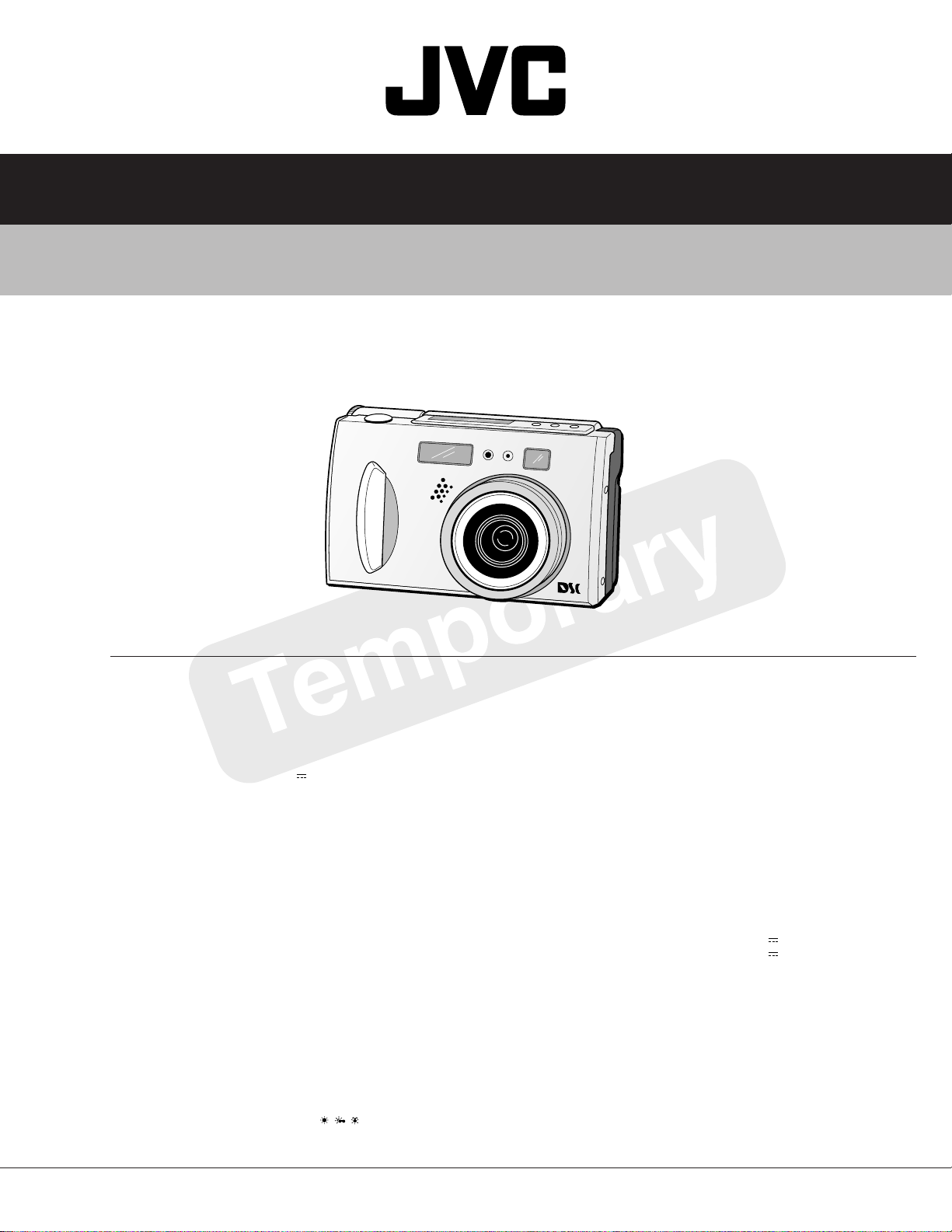
DIGITAL STILL CAMERA
GC-QX3U
SPECIFICATIONS
Dimensions
Power consumption
Weight
Power source
Flash
Recommended distance for flash
LCD screen
Storage media
CCD
Recording pixels
Focal distance
Lens
Video
Recording format
Sensitivity
Iris value (F value)
Exposure control
Exposure compensation
Minimum subject distance
Light measurement system
Shutter type
Shutter speed
White balance
Focus
: 108 (W) mm x 64 (H) mm x 57 (D) mm
(4-5/16" x 2-9/16" x 2-1/4")
: 4.0 W (when the LCD screen is off)
5.6 W (when the LCD screen is on)
: Approx. 290 g (0.64 lbs)
(without a Memory card and battery)
: DC 5 V
: Built-in,
Auto/red-eye prevention/forced/disabled
: 2.3 m to 5.2 m
: 2.0 inch, cool polysilicon TFT, 200,000 pixels
: SmartMedia
: 3.34 million pixels (3.24 million valid pixels),
1/1.8" square pixels, primary color filter,
interlace scan CCD
: 2032 x 1536 (TIFF 9.5MB, FINE 1MB, STD 700KB)
1024 x 768 (TIFF 2.4MB, FINE 500KB, STD 300KB)
640 x 480 (TIFF 980KB, FINE 150KB, STD 80KB)
: 7.5 mm to 17.5 mm
(equivalent to 37mm to 86 mm on a 35 mm still camera)
: 2.3X optical zoom lens
: 160 x 120, 20 seconds (80KB – 200KB) JVC original
: Exif Ver. 2.1 (DCF compliant), TIFF (Uncompressed),
DPOF-compatible
: 80/160/320 (ISO compliant)
: F2.8/3.8, 5.6, 8, 11
: Program AE, iris priority AE
: +/–2EV (0.5EV steps)
: Approx. 2 cm to 50 cm (in Macro mode)
: Multi, spot
: Electronic shutter
: Auto (Program AE: 1/8 – 1/750, Iris priority AE: 1/4 – 1/750)
: Auto/Manual (
: Auto/Manual
TM
3.3V (up to 64MB)
, , , MWB)
This service manual is made from all recycled paper.
COPYRIGHT © 2000 VICTOR COMPANY OF JAPAN, LTD
No.XXXXX
XXXXX 2000
Page 2
SECTION 1
DISASSEMBLY
1.1 BEFORE ASSEMBLY AND DISASSEMBLY
1.1.1 Precautions
1. Be sure to remove the power supply unit prior to mounting and soldering of parts.
2. When connecting and disconnecting the connectors, be
careful not to damage the wire.
3. When replacing chip parts (especially IC parts), desolder
completely first (to prevent peeling of the pattern).
4. Tighten screws properly during the procedures.
Unless specified otherwise, tighten screws at a torque
of 0.1N•m (1.0 kgf•cm).
CAUTION!!
RISK OF ELECTRIC SHOCK
When disassembling the unit, electric hazards may
occur in some cases if the capacitor for strobe
emission (STROBE board C6512) has been charged.
Therefore be also very careful when performing repairs
and inspections.
It is recommended that operations be carried out after
waiting for more than ten minutes with the power
supply removed or after discharging the capacitor
forcibly.
Discharge the capacitor according to <NOTE 2> on
Page 1-3.
C6512 is located behind the STROBE board.
1.1.2 Assembly and disassembly
STEP
PART NAME
1 FRONT CASE Remove screws
REAR CASE
2 OPERATION UNIT Remove the Connector Remove screws NOTE 1
12 3 4 5
FIG.
NO.
Fig
1-2-1
r MAIN CN4001 OPERATION UNIT
Remove the TOP COVER 2 (115)
POINT
2(115), 3(156), 4(114), 1(116)
3 (116)
1 : Indicate the disassembly steps. When assembling,
perform in the reverse order of these steps. This
number corresponds to the number in the disassem-
bly diagram.
2 : Indicates the name of disassembly/assembly parts.
3 : Indicates the number in the disassembly diagram.
4 : Indicates parts and points such as screws, washers,
springs which must be removed during disassembly/
assembly.
Lock (L), soldering (SD), shield, connector, etc.
[Example]
• (115) = Remove the parts No 115 screw.
• (SD1) = Desoldering at the point SD1.
• a = Disconnect the connector/ML a .
5 : Precautions on disassembly/assembly.
PRECAUTIONS ON HANDLING
THE LITHIUM SECONDARY BATTERY
This unit is equipped with a coin type lithium secondary
battery.
Improper handling of this battery may cause heat to
be generated, damage, fires, or leakage. Always follow
the precautions below.
1 Do not short-circuit, disassemble, distort, nor heat
the battery.
2 Load the battery with its + and - poles connected
correctly.
3 Do not solder the battery itself.
4 When replacing parts, also refer to the numbers
listed in the Parts List of the manual.
5 Do not store the battery in direct sunlight and hot
and humid places.
6 When replacing the battery, handle it with care and
do not attempt to hold it with tweezers as it may
short-circuit.
7 When disposing the battery, wind tape around the
terminal to insulate the battery, and dispose the
battery according to the method prescribed.
1.1.3 Screws used in assembly of cabinet parts and
boards
The following Table 1-1-1 shows the symbols, shapes, and
parts numbers of the screws used in the disassembly and
assembly diagrams of cabinet parts and board assemblies.
Prior to assembly, check the following table and be sure to
use the correct screw.
SHAPE PARTS NO.SYMBOL COLOR
101E
114
115
116
117
153F
155
156
LY30018-019A Black
LY30018-060A Silver
LY30018-010A Black
LY30018-023A Black
LY30019-025A Gold
QYSPSGT1740Z Gold
LY30018-056A Silver
LY30018-059A Silver
Table 1-1-1
1-1
Page 3
1.1.4 Disconnection of Connectors (Wires)
FRONT CASE
REAR CASE
OPERATION UNIT
STROBE BOARD ASSEMBLY
JACK BOARD ASSEMBLY
LCD MODULE
MAIN BOARD ASSEMBLY
MONI/REG BOARD ASSEMBLY
OP UNIT
1
2
3
4
5
6
7
Torque driver
YTU94088
12
Clip IC replacement jig
PTS40844-2
Connector catcher
YTU94036A
34
Soldering kit
YTU96016B
Connector
Pull both ends of the connector in the arrow direction, remove the lock and disconnect the flat wire.
Flat wire
Connector 1
Fig. 1-1-1 Connector 1
Flat wire
Connector 2
Fig. 1-1-2 Connector 2
Extend the locks in the direction of the arrow for unlocking
and then pull out the wire. After removing the wire,
immediately restore the locks to their original positions
because the locks are apt to come off the connector.
1.2 TOOLS AND EQUIPMENTS REQUIRED FOR
ADJUSTMENTS
1.2.1 Tools required for adjustments
1.3 DISASSEMBLY/ASSEMBLY OF CABINET PARTS
1.3.1 Disassembly flow chart
The following flow chart shows the steps for disassembling
the cabinet parts. To assemble, perform the steps of the flow
chart in the reverse order.
The encircled numbers indicate the order for disas-
Note:
sembling the cabinet parts.
The screw numbers indicate the disassembling order.
Flat wire
Connector 3
Fig. 1-1-3 Connector 3
B-B connector
Pull the board by both the sides in the direction of the arrow
for disconnecting the B-B connector.
Fig. 1-1-4 Connector 4
Connector 4
1-2
Page 4
1.3.2 Disassembly method
STEP
1 FRONT CASE Remove screws
REAR CASE 2 (115), 3 (156), 4 (114), 1 (116)
2 OPERATION UNIT Remove the Connector Remove screws NOTE 1
3 STROBE BOARD ASSEMBLY Remove the Connector Remove screw NOTE 1
JACK BOARD ASSEMBLY Remove the Connector Remove screws
4 LCD MODULE Remove the Connector Remove screws NOTE 1
5 MAIN BOARD ASSEMBLY Remove the Connector NOTE 1
MONI/REG BOARD ASSEMBLY Remove the PWB HOLDER Remove screws 2 (114)
6 OP UNIT Remove from the Frame Assy Remove screws 3 (117)
PART NAME
Fig
1-2-1
Fig
1-2-1
Fig
1-2-2
r MAIN CN4001
Remove the TOP COVER 2 (115)
n MAIN CN6601
p MAIN CN5501
m LCD MODULE (BL)
k MAIN CN3002
Remove from the Frame Assy
Remove from the LCD Holder
h MAIN CN501
c MAIN CN3001
d MON/REG TL9001
Remove from the CCD BOARD CN1001 20Pin (SD2)
OPERATION UNIT 3 (116)
STROBE CN6501 1 (114) NOTE 2
JACK CN101 2 (114)
LCD MODULE (LCD) 2 (114)
OP UNIT
MON/REG CN9001
Frame Assy d (SD1)
POINTFIG. NO.
JACK CN701 e (SD3), f (SD4), g (SD5)
CONNEC- NO.OF
TOR/HL PINS
c
80 MAIN Board CN3001
d
1 MONI/REG Board TL9001
e
1 JACK Board TP3
f 1 JACK Board TP2
g
1 JACK Board TP1
h
22 MAIN Board CN501
j
2 MAIN Board CN502
k
24 MAIN Board CN3002
m 2 JACK Board CN701
n
14 MAIN Board CN6601
p 38 MAIN Board CN5501
q
28 MAIN Board CN2001
r 12 MAIN Board CN4001
s
t
STROBE UNIT WIRE (ORANGE)
1
STROBE UNIT WIRE (BROWN)
1
CONNECTION
MONI/REG Board CN9001
MAIN FRAME (RED)
MAIN FRAME (BROWN)
MONI/REG Board J9001 (BLACK)
MONI/REG Board J9002 (RED)
OP UNIT
OP UNIT
LCD MODULE (LCD)
LCD MODULE (BL)
STROBE Board CN6501
JACK Board CN101
CCD Board CN1001
OPERATION UNIT
STROBE Board J6501 (Through hole)
STROBE Board J6502 (Through hole)
<NOTE 1>
Destination of connectors
Three kinds of double-arrows in connection tables
Note:
respectively show kinds of connector/wires.
: Board to Board connector
: Flat wire
: Wire
<NOTE2>
Be careful from electric shock hazard because the capacitor
(C6512) for the strobe is exposed. Be sure to positively discharge the capacitor if it is energized by short-circuiting a
resistor (10 - 22 kΩ ) connected at both capacitor terminals.
Please be very careful when doing this job.
1-3
u
1 STROBE UNIT WIRE (RED)
v
w
x
STROBE UNIT WIRE (BLACK)
1
STROBE UNIT WIRE (Red, Thin wire) STROBE Board J6505 (Through hole)
1
STROBE UNIT WIRE (BLACK, Thin wire)
1
STROBE Board J6503 (Through hole)
STROBE Board J6504 (Through hole)
STROBE Board J6506 (Through hole)
Page 5
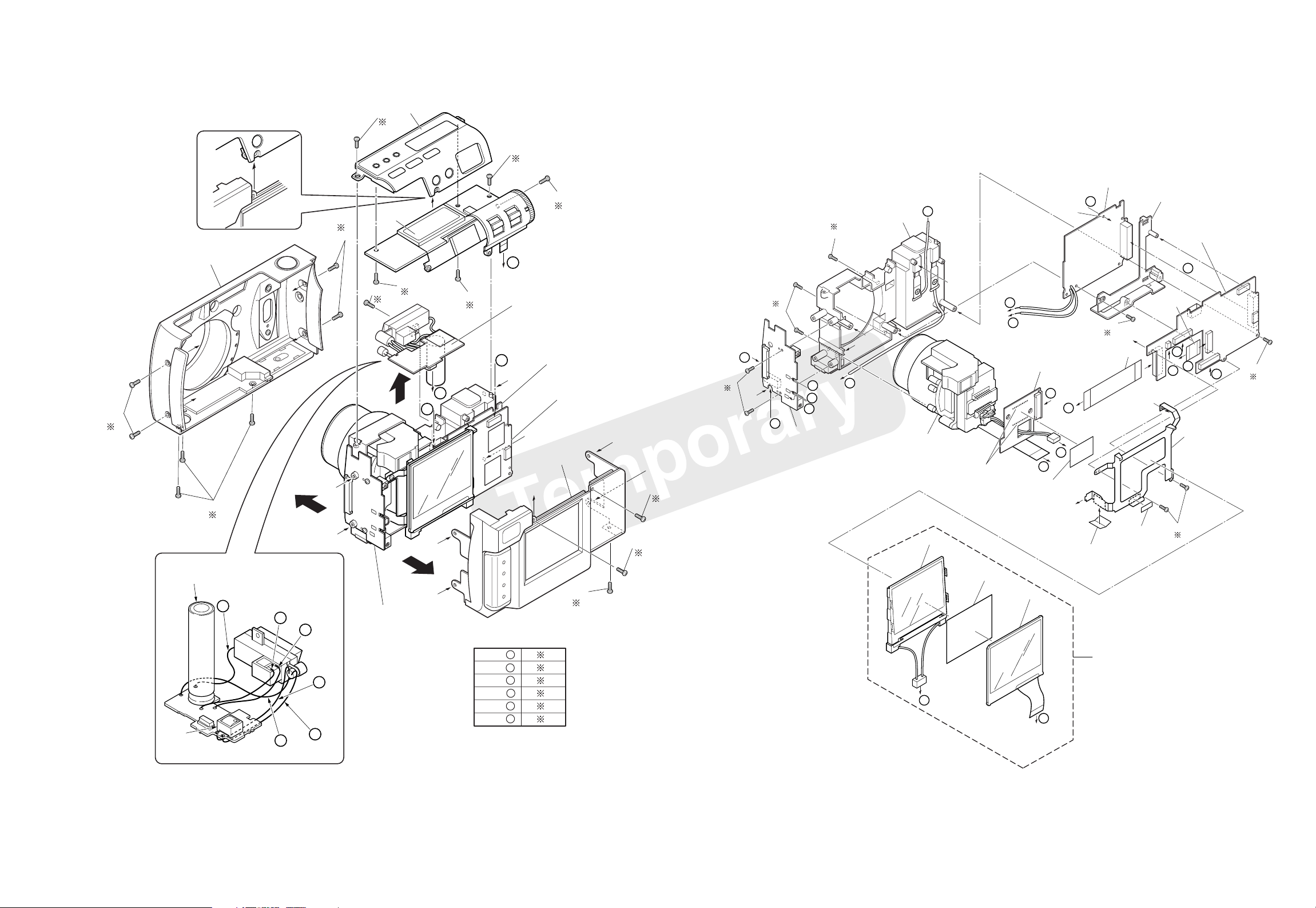
116
114
117
117
F
101
103
114
B
A
C
j
p
p
q
g
e
e
d
B
C
m
f
g
f
j
h
q
k
c
CCD BOARD ASSY
< 03 >
MAIN BOARD ASSY
< 01 >
MONI/REG BOARD ASSY
< 02 >
JACK BOARD ASSY
< 04 >
114
109
107B
105
107C
107A
107
104
106
113
(SD2)
(SD1)
(SD3)
(SD4)
(SD5)
102
A
108
114
k
m
h
d
5
5
6
6
3
4
110
2
116
2
D
116
2
111
1
155
153
G
114
H
E
F
156
1
C6512
L6501
114
E
u
t
v
F
x
JACK BOARD ASSY
< 04 >
w
1
s
115
2
3
n
n
E
F
115
2
Remove screw marks
r
STEP 1
STEP 2
STEP 3
STEP 4
STEP 5
STEP 6
r
STROBE
BOARD ASSY
< 05 >
MONI/REG BOARD ASSY
< 02 >
G
MAIN BOARD ASSY
< 01 >
H
152
D
114
1
1
2
3
4
5
6
G
H
116
1
156
1
Fig.1-3-1
1-4
1-5
Fig.1-3-2
Page 6
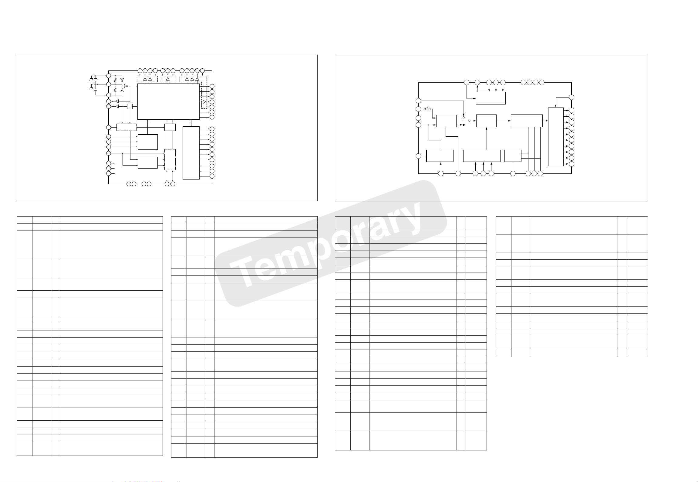
1.4 IC BLOCK DIAGRAM
1.4.1 IC 1002 (CXD2497R)
1.4.2 IC 2001 (CDS/AGL)
3
DD
V
OSCI
28
OSCO
27
CKI
26
25
CKO
MCKO
SNCSL
SSI
SCK
SEN
SSGSL
RST
TEST1
TEST2
30
3
31
32
33
6
2
37
48
Selctor
1/2
Register
1
5
DD
DD
V
V
Pin Descriptions
Pin No. Pin Name I/O Description
1VSS1 - GND
2 RST I System reset input terminal H: Reset released L: Reset
activated
(Should be activated at power ON, normally.)
(Schmitt trigger input/without protection diode on power
supply side)
3 SNCSL I Sync system switching control input terminal
(with pull-down resistor)
H: CKI sync L: MCKO sync
4 ID O Line identification pulse output terminal in the vertical
direction
5 WEN O Memory write timing pulse output terminal
6 SSGSL I Built-in SSG enable input terminal (with pull-down
resistor)
H: Built-in SSG is effective. L: External sync is effective.
7VDD1 - 3.3V power (for common logic section)
8VDD2 - 3.3V power (for RG terminal)
9 RG O Reset gate pulse output terminal for CCD
10 VSS2 - GND
11 VSS3 - GND
12 H1 O Clock output terminal for CCD horizontal register
13 H2 O Clock output terminal for CCD horizontal register
14 VDD3 - 3.3V to 5.0V power (for H1 and H2 terminals)
15 VDD4 - 3.3V power (for CDS system terminals)
16 XSHP O CCD pre-charge level sample/hold pulse output terminal
17 XSHD O CCD data level sample/hold pulse output terminal
18 XRS O Sample/hold pulse output terminal for phase matching in
analog-to-digital conversion
19 PBLK O Pulse output terminal for pulse cleaning during
horizontal and vertical blanking period
20 CLPDM O Pulse output terminal for CCD dummy signal clamping
21 VSS4 - GND
22 OBCLP O Pulse output terminal for CCD optical black signal
23 ADCLK O Clock output terminal for analog-to-digital conversion IC
Logical phase is adjustable with the serial interface data
H1H2V
SSG
1
5
SS
SS
V
V
2
3
DD
SS
V
11
Pulse Generator
35361297
Latch
HD
RG
Selector
34
VD
4
2
DD
SS
V
V
XSHP
V Driver
XSHD
181716151098 21131214
XRS
4
SS
V
19
PBLK
CLPDM
20
22
OBCLP
23
ADCLK
24
SS
5
V
4
ID
5
WEN
41
V1A
43
V1B
39
V2
44
V3A
46
V3B
40
V4
47
SUB
VH
42
VM
38
VL
45
24 VSS5 - GND
25 CKO O Inverter output terminal
26 CKI I Inverter input terminal
27 OSCO O Inverter output terminal for oscillation (If not used,
should be opened or connected to GND through a
capacitor.)
28 OSCI I Inverter input terminal for oscillation (If not used, should
be fixed to "Low".)
29 VDD5 - 3.3V power (for common logic section)
30 MCKO O System clock output terminal for signal processing IC
31 SSI I Serial interface data input terminal for setting each IC
mode (Schmitt trigger input/without protection diode on
power supply side)
32 SCK I Serial interface clock input terminal for setting each IC
mode (Schmitt trigger input/without protection diode on
power supply side)
33 SEN I Serial interface strobe input terminal for setting each IC
mode (Schmitt trigger input/without protection diode on
power supply side)
34 VD I/O Vertical sync signal input/output terminal
35 HD I/O Horizontal sync signal input/output terminal
36 VSS6 - GND
37 TEST1 I IC test terminal 1 with pull-down resistor (Should be
fixed to GND normally.)
38 VM - GND (for vertical drivers)
39 V2 O Clock output terminal for CCD vertical register
40 V4 O Clock output terminal for CCD vertical register
41 V1A O Clock output terminal for CCD vertical register
42 VH - 15.0V power (for vertical drivers)
43 V1B O Clock output terminal for CCD vertical register
44 V3A O Clock output terminal for CCD vertical register
45 VL - -7.5V power (for vertical drivers)
46 V3B O Clock output terminal for CCD vertical register
47 SUB O Pulse output terminal for CCD electronic shutter
48 TEST2 I IC test terminal 2 with pull-down resistor (Should be
fixed to GND normally.)
21
27
ADCIN
25
CDSSW
26
CDSIN
BLKSH
BLKFB
28
29
CDS PGA
DC offset
compensatory
17
20
OBP
PBLK
Pin Descriptions
Pin No. Pin Name Description I/O
Analog (A) or
1 NC No internal connection - 2 D0 Digital output terminal (LSB) O D
3-10 D1-D8 Digital output terminals O D
11 D9 Digital output terminal (MSB) O D
12 NC No internal connection - 13 OADCLK Latch clock output terminal for D0 to D9 O D
14 DVSS Digital GND (0V) - D
15 DV
DD Power for digital 3.0V system - D
(Should be connected to AVDD outside the IC.)
16 ADCLK Analog-to-digital conversion clock input terminal I D
17 OBP Optical black pulse input terminal I D
18 SPBLK Black level sampling clock input terminal I D
19 SPSIG Signal level sampling clock input terminal I D
20 PBLK Pre-blanking signal input terminal I D
21 OADSW OADCLK enable input terminal I D
22 AVSS Analog GND (0V) - A
23 AVDD Power for analog 3.0V system - A
24 NC No internal connection - 25 CDSSW Signal level sampling output terminal O A
26 CDSIN CDS input terminal I A
27 ADCIN ADC input terminal I A
28 BLKSH Black level sample/hold terminal - A
29 BLKFB Black level feedback terminal - A
30 AVSS Analog GND (0V) - A
31 AVDD Power for analog 3.0V system - A
(Should be connected to DVDD outside the IC.)
32 VRT Reference voltage terminal 3 - A
(Ceramic capacitor of 0.1µF or more should be
connected between this terminal and AVss.)
33 VRB Reference voltage terminal 2 - A
(Ceramic capacitor of 0.1µF or more should be
connected between this terminal and AVss.)
OADSW
OADCLK
13 16 18 19
Serial
Interface
44
SCK
Digital (D)
ADCLK
SPBLK
TIMING
gen
43CS45
SDATA
SPSIG
Occurrence
Bias
35
BIAS
41
AVDDDVDD
46
10bit
ADC
33
VRT
AVSS
DVSS
40
48
42 OEB
11 D9
10 D8
9D7
Output
Latch
circuit
32
34
VRB
VRM
8D6
7D5
6D4
5D3
4D2
3D1
D0
2
34 VRM Reference voltage terminal 1 - A
(Ceramic capacitor of 0.1µF or more should
be connected between this terminal and AVss.)
35 BIAS Internal bias terminal - A
(A 24-Kohm resistor should be connected
between this terminal and AVss.)
36 NC No internal connection - 37 AVSS Analog GND (0V) - A
38 AV
DD Power for analog 3.0V system - A
(Should be connected to DVDD outside the IC.)
39 NC No internal connection - 40 AVSS Analog GND (0V) - A
41 AVDD Power for analog 3.0V system - A
(Should be connected to DVDD outside the IC.)
42 OEB Digital output enable control input terminal I D
43 CS Serial interface control input terminal I D
44 SCK Serial clock input terminal I D
45 SDATA Serial data input terminal I D
46 DVDD Power for digital 3.0V system - D
(Should be connected to AVDD outside the IC.)
47,48 DVSS Digital GND - D
1-6
1-7
Page 7
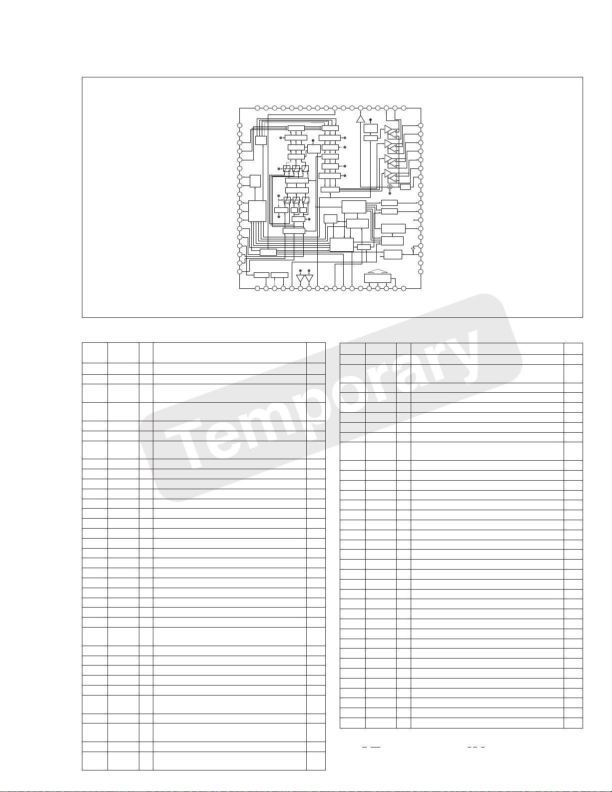
1.4.3 IC 7302 (CXA3268AR)
VSSVSSTST10
TST9
51 38 37
V
SSVSS
+3.0V
55
V
DD
56
TST11
OSD B
OSD R
OSD G
HCK1
HCK2
VCC1
FIL IN
B/B-Y
R/R-Y
57
58
59
60
NC
61
HCK
GEN
62
+3.0V
63
64
HST
HCOUNTER
HPULSE
65
EN
GEN
66
VCK
67
VST
67
RGT
69
70
71
G/Y
72
H.FILTER SYNC SEP
SS
V
CONTRAST
S/H
CONT
GEN
GR
MODE
PIC-G
PIC-F
MODE
SS
V
FIL OUT
SYNC IN
SYNC OUT
Pin Descriptions
Pin No. Pin Name I/O Description
1 Vss - GND terminal for digital 3.0V system
2 FIL OUT O H filter output terminal (for internal sync separator use)
3 SYNC IN I Sync input terminal for sync separator circuit
(for internal sync separator use)
4
SYNC OUT
O Sync output terminal for sync separator circuit
(for internal sync separator use)
5
CSYNC/HD
I CSYNC/horizontal sync signal input terminal
6 DA OUT O DAC output terminal
7 REF O Level shifter circuit reference voltage output terminal for
LCD panel
8 F ADJ O f0 adjust resistor connecting terminal for TRAP
9 GND1 - GND terminal for analog 3.0V system
10 VD I Vertical sync signal input terminal
11 DWN O Up/Down switching signal output terminal
12 WIDE O 16:9 wide display switching pulse output terminal
13 TST1 - Test terminal (Should be opened.)
14 SCK I Serial clock input terminal
15 SEN I Serial load input terminal
16 SDAT I Serial data input terminal
17 R INJECT O Resistor connecting terminal for serial block current control
18 VSS - GND terminal for digital 3.0V system
19 VDD - Power for digital 3.0V system
20 VDD - Power for digital 3.0V system
21 CKO O Oscillation cell output terminal
22 CKI I Oscillation cell input terminal
23 Vss - GND terminal for digital 3.0V system
24 RPD O Phase comparison output terminal
25 XCLR I Capacitor connecting terminal for power-on reset (for
timing generating system)
26 VDO O VDO pulse output terminal
27 HDO O HDO pulse output terminal
28 TST2 - Test terminal (Should be connected to GND.)
29 GND2 - GND terminal for analog 12.0V system
30 SIG.C I DC voltage adjust terminal for R, G, B and PSIG outputs
31 B DC DET O Capacitor connecting terminal for B signal's DC voltage
feedback circuit
32 B OUT O B signal output terminal
33 R DC DET O Capacitor connecting terminal for R signal's DC voltage
feedback circuit
34 R OUT O R signal output terminal
35 G DC DET O Capacitor connecting terminal for G signal's DC voltage
feedback circuit
TST8
OSD RGB
TRAP
LPF
CLAMP
MATRIX
DL1PICTURE
HUE
CLAM[P
SYNC/HD
TST7
DL1
COLOR
DA
Buf Buf
DA OUT
FILTER
FILTER
B
BGR
HUE
CLP
REF
Input
TST6
LPF
BIAS
REF
Res.
L
H
TST5NCPOF
S/H
USER-BRIGHT
GAMMAM
CLAMP
BLK-LIM
SUB-BRIGHT
POL SW
PULSE
ELM
V COUNTER
GND1
F ADJ
GND1
VD
U-GRT
γ1γ2
WHITLIM
SUB-CONT R
SUB-CONT B
BLKLIM
SUB-BRT R
SUB-BRT B
TST4
GND3
PLL
COUNTER
V CONTROL
V POSITION
DWN
GND3
WIDE
COM
Buf
V SEP
TST1
3
CC
V
+12.0V +12.0V
PSIGBRT
PSIGBRIGHT
POL SW
S/P CONV
REGISTER DAC
SCK
TST3
394041424344454647484950525354
Buf
Buf
Buf
Buf
COM-DC
HDO GEN
VDO GEN
COMPARATOR
HSYNC DET
H SKEW DET
CLK
1615141312111098765321 4 17 18
SEN
PSIG OUT
PHASE
CK
CONTROL
SDAT
2
CC
PSIG DC DET
V
SIG.C
MCK
V
SS
SS
V
R INJECT
+3.0V
+3.0V
GND2
V
36
G OUT
35
G DC OUT
34
R OUT
33
R DC DET
32
B OUT
31
B DC DET
30
SIG. C
29
GND2
28
TST2
27
HDO
26
VFO
25
XCLR
24
RPD
23
SS
SS
V
22
CKI
21
CKO
20
DD
V
19
V
DD
36 G OUT O G signal output terminal
37 VCC2 - Power for analog 12.0V system
38 PSIG DC O Capacitor connecting terminal for G signal's DC voltage
DET feedback circuit
39 PSIG OUT O PSIG output terminal
40 TST3 - Test terminal (Should be opened.)
41 VCC3 - Power for analog 12.0V system COM (CS)
42 COM O
Common electrode voltage output terminal (CS) for LCD panel
43 GND3 - GND terminal for analog 12.0V system COM (CS)
44 TST4 - Test terminal (Should be opened.)
45 POF O LCD panel power ON/OFF terminal
(Open, if this function is not used.)
46 NC - No internal connection
47 TST5 - Test terminal (Should be connected to GND.)
48 TST6 - Test terminal (Should be connected to GND.)
49 TST7 - Test terminal (Should be opened.)
50 TST8 - Test terminal (Should be opened.)
51 TST9 - Test terminal (Should be opened.)
52 TST10 - Test terminal (Should be opened.)
53 VSS - GND terminal for digital 3.0V system
54 VSS - GND terminal for digital 3.0V system
55 VDD - Power for digital 3.0V system
56 TST11 - Test terminal (Should be connected to GND.)
57 OSD B I OSD B input terminal
58 OSD R I OSD R input terminal
59 OSD G I OSD G input terminal
60 NC - No internal connection
61 HCK1 O H clock pulse 1 output terminal
62 HCK2 O H clock pulse 2 output terminal
63 VCC1 - Power for analog 3.0V system
64 HST O H start pulse output terminal
65 EN O EN pulse output terminal
66 VCK O V clock pulse output terminal
67 VST O V start pulse output terminal
68 RGT O Right/Left switching signal output terminal
69 FIL IN I H FILTER input terminal (for internal sync separator use)
70 B/B-Y I B/B-Y signal input terminal
71 G/Y I G/Y signal input terminal
72 R/R-Y I R/R-Y signal input terminal
* DWN:
DOWN SCAN and UP SCAN RGT: RIGHT SCAN and LEFT SCAN
H: Pull-up resistor incorporated L: Pull-down resistor incorporated
1-8
Page 8
1.4.4 LCD (ACX301AK)
BGRBRG
RBGRGB
RBGRGB
BGRBRG
RBGRGB
V shift register
COM
V Level shifter
Electrode
1 2 3 4 5 6 7 8 9 10 11 12 13 14 15 16 17 18 19 20 21 22 23 24
TESTL
Pin Descriptions
Pin No. Pin Name Description
1 TESTL Panel testing terminal (Should be opened.)
2 COM Common electrode voltage input terminal for panel
3 VST Start pulse input terminal for V shift register drive
4 VCK Clock input terminal for V shift register drive
5 EN Enable signal input terminal for gate select pulse
6 DWN Drive direction signal input terminal for V shift register
7VVDD Power for V driver
8VSS GND for H and V drivers
9HVDD Power for H driver
10 VSSG Negative voltage setting terminal for V driver
11 TEST2 Connected to GND through a 1-Mohm resistor in the panel
12 WIDE Pulse input terminal for 16:9 mode
13 HST Start pulse input terminal for H shift register drive
14 REF Level shifter circuit reference voltage input terminal
15 TEST Panel testing terminal (Should be opened.)
16 Cext/Rext Power input terminal for setting H shift register drive time
constant
17 HCK2 Clock input terminal for H shift register drive
18 HCK1 Clock input terminal for H shift register drive
19 PSIG Uniformity improving signal input terminal
20 GREEN Video signal (G) input terminal for the panel
21 RED Video signal (R) input terminal for the panel
22 BLUE Video signal (B) input terminal for the panel
23 RGT Drive direction signal input terminal for H shift register
24 TESTR Panel testing terminal (Should be opened.)
COM
EN
VST
VCK
DWN
H Level shifter & Shift register
LCCs
Negative
Voltage
Occurence
Circuit
VSS
VVDD
VSSQ
HVDD
TEST2
COM
HST
WIDE
REF
TEST
HCK2
Cext/Rext
HCK1
PSIG
GREEN
RED
BLUE
RTG
TESTR
Features
• Device Structure
- Active matrix panel with internal driver using lowtemperature polysilicon transistors
- Pixels
Total dots: 896 (H) x 230 (V) =206,080
Display dots: 880 (H) x 228 (V) =200,640 (2.0 in.)
• Total dots: 200,000 dots 5.1cm diagonal (2.0 in.)
• Horizontal resolution: 440 TV scanning lines
• Light permeability: 5.6% (standard)
• Smooth screen image with RGB delta array
• NTSC/PAL compatible
• High image quality internal circuitry
• 16:9 screen display function
• Low-reflection screen display processing assures easy
viewing even outdoors
• Anti-grime display
Delta array
1-9
Page 9
1.4.5 CCD (ICX262AQ)
11
V
DD
10
V
OUT
12
ØRG
9
GND
13
H
Ø2
8
TEST
14
H
Ø1
7
TEST
15
GND
6
V
Ø1B
16
5
V
Ø1A
17
C
SUB
4
V
Ø2
18
V
L
3
V
Ø3B
19
H
Ø1
2
V
Ø3A
20
H
Ø2
1
V
Ø4
B
Gr
B
Gr
B
Gr
Gb
R
Gb
R
Gb
Gb
B
Gr
B
Gr
B
Gr
Gb
R
Gb
R
Gb
R
Vertical register
Horizontal register
(NOTE)
(NOTE)
: Photo Sensor
Pin Descriptions
Pin No. Pin Name Description
1Vø4 Vertical register transfer clock
2Vø3A Vertical register transfer clock
3Vø3B Vertical register transfer clock
4Vø2 Vertical register transfer clock
5Vø1A Vertical register transfer clock
6Vø3B Vertical register transfer clock
7 TEST Test terminal*
8 TEST Test terminal*
1
1
9 GND GND
10 VOUT Signal output
11 VDD Circuit power
12 øRG Reset gate clock
13 Hø2 Horizontal register transfer clock
14 Hø1 Horizontal register transfer clock
15 GND GND
16 øSUB PCB clock
17 CSUB PCB bias*
2
18 VL Protection transistor bias
19 Hø1 Horizontal register transfer clock
20 V
ø2 Horizontal register transfer clock
*1: Terminal should be opened.
*2: A 0.1µF capacitor should be connected between the pin and GND, since the
DC bias is generated inside the CCD.
Features
• Field period readout system
• Interline CCD image sensor
• Total number of pixels: 2140 (H) x 1560 (V) approx. 3340k
pixels
• Number of effective pixels: 2088 (H) x 1550 (V) approx.
3240k pixels
• Effective number of pixels: 2080 (H) x 1542 (V) approx.
3210k pixels (1.18in)
• Chip size: 8.10mm (H) x 6.64mm (V)
• Unit cell size: 3.45µ␣ m (H) x 3.45µ␣ m (V)
• Optical black:
Horizontal (H) direction : front 4 pixels, rear 48 pixels
Vertical (V) direction : front 8 pixels, rear 2 pixels
• Number of dummy bits: Horizontal 28 Vertical 1 (even fields
only)
• Square pixels
• Horizontal drive frequency: 18kHz
• RGB basic color mosaic on-chip color filter
• High sensitivity
• Cyclic, variable speed shutter
• Excellent anti-blooming characteristics
1pin
2
V
8
4
11pin
H
48
Optical black wiring diagram
(Top View)
1-10
Page 10

SECTION 2
ELECTRICAL ADJUSTMENT
2.1 ELECTRICAL ADJUSTMENT
2.1.1 Precautions
Both the camera section and deck section of this model
are designed and manufactured to be adjustment-free.
However, if both or either of the following parts is replaced,
it needs special adjustment with a personal computer at a
JVC service equipment after the part replacement
• OP block assembly
• EEPROM (on the MAIN board)
When there is some trouble in the electric circuit, it is required
to detect the faulty part with specified test instruments first
and then to proceed to repair, replacement and adjustment.
1. When cheking a signal at a chip test point, be sure to use
an IC clip or the like not to apply any stress to the test point.
When replacing a chip part (IC in particular), completely
remove solder chips from it and its periphery before
proceeding to part replacement (in order to avoid exfoliation
of the pattern).
2. Carefully disconnect/connect connectors because they
are apt to get damaged.
2.1.2 Test instruments 0required for electrical
adjustment
12
34
Patch cord
YTU93099A
Service support system
YTU94057-47
Jig connector cable
YTU93102A
PC cable
QAM0099-002
12
14
Gray scale chart
YTU94133A
Cleaning cloth
KSMM-01
Smart media card
16MB
Light box assembly
910
11
13
YTU93096A
Color bar chart
YTU94133C
USB
QAM0252-001
2.1.3 Required test equipment
1. Color TV monitor.
2. AC power adapter (AA-V37 or equivalent)
3. Oscilloscope (dual-trace type, for more than 20 MHz).
4. Digital voltmeter
5. Frequency counter (with threshold level adjuster)
6. Personal computer
2.1.4 Setup (LCD ADJUSTMENT)
Setup for electrical adjustment with personal computer
Note 1:
As a general rule for adjustment with a personal
computer, connect a personal computer to its
PRINTER terminal.
Note 2:
Use DC cord to supply the power.
Jig connector cable
5
78
YTU93091B
INF adjustment lens
YTU92001B
Extension connector
6
Camera stand
YTU94145A
YTU93079
2-1
PRINTER
PC cable
QAM0099-002
Service support system
YTU94057-47
RS-232C
port
MENU
Personal computer
Fig. 2-1-1 Setup for electrical adjustment with
personal computer (I)
Page 11

Extension connector
Personal computer
USB
port
Service support system
YTU94057-47
16MB
Smart media
Card
MENU
USB
Note) It is needs to connect
the extension
double for use the DC
cord(coupler)
Jig connector cable
(YTU93091B)
Fig. 2-1-2 Setup for electrical adjustment with
personal computer (II)
Pin No. FUNCTION
1 135TMS
2 135TDI
3 nTRST
4 AL_3.3V
5 32DBI
6 GND
7 M_COM
8 M_SIG_C
9 M_RED
10 M_SIG_GND
11 JTAGMODE
12 135TDO
13 135TCK
14 AL_3.3V
15 32RST
16 M_BLUE
17 RPD
18 M_PSIG
19 M_GREEN
20 NC
connector
2.1.5 Setup (CCD ADJUSTMENT)
Setup for electrical adjustment with personal computer
Note 1:
As a general rule for adjustment with a personal
computer, connect a personal computer to its
USB terminal.
Note 2:
Use DC cord to supply the power.
Fig. 2-1-3 Setup for electrical adjustment with
personal computer (I)
Table 2-1-1 Jig Connector Function
2-2
Page 12

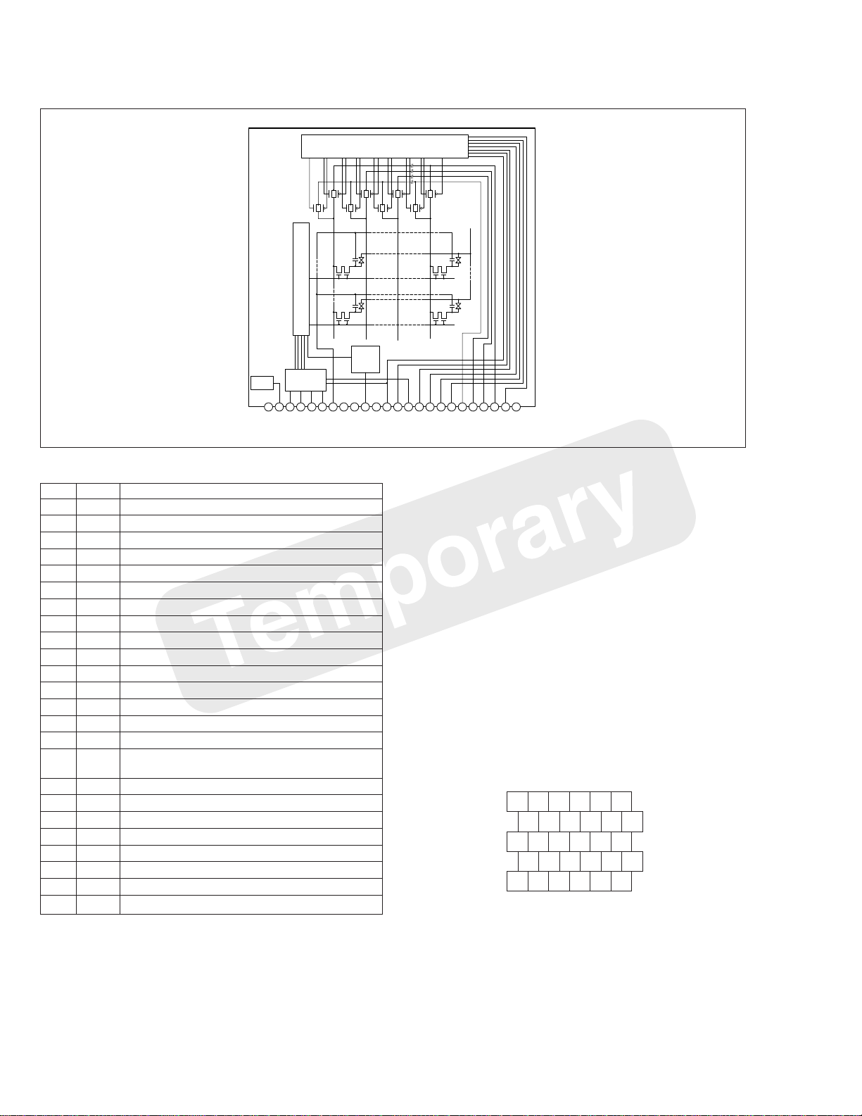
3.2 BOARD INTERCONNECTION
NOTE : When ordering parts, be sure to order according
to the Part Number indicated in the Parts List.
3-3 3-4
Page 13

3.3 MAIN (SYSCON) SCHEMATIC DIAGRAM
NOTE : When ordering parts, be sure to order according
to the Part Number indicated in the Parts List.
3-5 3-6
❈ MARK IS NOT USED
Page 14

3.4 MAIN (DSP96) SCHEMATIC DIAGRAM
NOTE : When ordering parts, be sure to order according
to the Part Number indicated in the Parts List.
3-7 3-8
❈ MARK IS NOT USED
Page 15

3.5 MAIN (DSP97) SCHEMATIC DIAGRAM
NOTE : When ordering parts, be sure to order according
to the Part Number indicated in the Parts List.
3-9 3-10
❈ MARK IS NOT USED
Page 16

3.6 MAIN (G/A JCY0148) AND MAIN (SD SUB) SCHEMATIC DIAGRAM
3.7 MAIN (F/Z MDA) ANDMAIN (IRIS) SCHEMATIC DIAGRAMS
NOTE : When ordering parts, be sure to order according
to the Part Number indicated in the Parts List.
NOTE : When ordering parts, be sure to order according
to the Part Number indicated in the Parts List.
❈ MARK IS NOT USED
❈ MARK IS NOT USED
3-11 3-12
Page 17

3.8 MAIN (CCD AGC A/D AND ARM ROM) SCHEMATIC DIAGRAM
3.9 MAIN (STROBE CONTROL AND STROBE FLASH) SCHEMATIC DIAGRAM
NOTE : When ordering parts, be sure to order according
to the Part Number indicated in the Parts List.
NOTE : When ordering parts, be sure to order according
to the Part Number indicated in the Parts List.
❈ MARK IS NOT USED
3-13 3-14
❈ MARK IS NOT USED
Page 18

3.10 CCD SCHEMATIC DIAGRAM
3.11 MONI REG (MONITOR) SCHEMATIC DIAGRAMS
NOTE : When ordering parts, be sure to order according
to the Part Number indicated in the Parts List.
NOTE : When ordering parts, be sure to order according
to the Part Number indicated in the Parts List.
❈ MARK IS NOT USED
❈ MARK IS NOT USED
3-15 3-16
Page 19

3.12 MONITOR REG (DC/DC) SCHEMATIC DIAGRAMS
NOTE : When ordering parts, be sure to order according
to the Part Number indicated in the Parts List.
3-17 3-18
❈ MARK IS NOT USED
Page 20

3.13 JACK(VIDEO OUT/USB/PRINTER/DC JACK) AND MONITOR BACK LIGHT SCHEMATIC DIAGRAM
NOTE : When ordering parts, be sure to order according
to the Part Number indicated in the Parts List.
- WAVEFORM -
(Page 3-19)
❈ MARK IS NOT USED
3-19 3-20
Page 21

SECTION 4
5
PARTS LIST
SAFETY PRECAUTION
Parts identified by the symbol are critical for safety. Replace only with specified part numbers.
4.1 PACKING AND ACCESSORY ASSEMBLY <M1>
The instruction manual to be provided with this product will differ according to the destination.
17
AC POWER ADAPTER
AA-V37U
(Refer to Sec.5)
8
18
FINAL ASSY <M2>
(GC-QX3U)
6
16
BATTERY PACK
(BN-V37U)
5A
2
7
4
3
25
9
10
27
21
24
26
28
35
31
32
33
1
LABEL
(SERIAL)
# REF No. PART No. PART NAME, DESCRIPTION # REF No. PART No. PART NAME, DESCRIPTION
--------------- ----------------------- ----------------------------------------------------- ---------------- ----------------------- ------------------------------------------------------
✽✽✽✽✽✽✽✽✽✽✽✽✽✽✽✽✽✽✽✽✽✽✽✽✽✽✽✽✽✽
PACKING AND ACCESSORY ASSEMBLY <M1>
1 LY31465-002A PACKING CASE
2 LY30023-016A POLY BAG
3 LY31466-001A CUSHION
4 LY42548-001A SHEET
5 LY31822-001A HOOD(OP)
5A QPA01001505 POLY BAG
6 PEAC0449 DC PLUG CORD
7 PEAC0496 VIDEO CABLE
8 QAM0252-001 USB CABLE
9 LY31074-007A CD ROM ASSEMBLY
10 BT-51020-2 REGIST.CARD
16 QQR0491-002 CORE FILTER
17 QQR0491-001 CORE FILTER,x2
18 QQR0917-002 CORE FILTER
21 QPA02003006 POLY BAG
24 LY30663-001A HAND STRAP
25 LY31468-002A LENS CAP
26 LY42313-001A STRING
27 LY31737-001A MEDIA CARD ASSEMBLY
28 BT-51005-4 WARRANTY INF.
31 LYT0543-001A INST.BOOK(EN)
32 LYT0543-002A INST.BOOK(FR)
33 LYT0543-003A INST.BOOK(SP)
35 LYT0543-005A SHEET(HOOD)
4-1
4-2
Page 22

FINAL ASSEMBLY
153
<M2>
153C
116
110
111
BEWARE OF BOGUS PARTS
Parts that do not meet specifications may cause trouble
in regard to safety and performance. We recommend that
116
116
D
genuine JVC parts be used.
156
153B
E
153D
153A
112
115
G
H
F
114
114
116
E
p
F
m
155
116
153E
116
117
e
f
g
JACK BOARD ASSY
< 04 >
114
117
e
n
101A
A
C
115
101D
B
102
r
STROBE
BOARD ASSY
< 05 >
d
101C
G
H
CCD BOARD ASSY
< 03 >
101B
101E
101E
f
g
h
113
101
MONI/REG BOARD ASSY
< 02 >
d
114
A
108
q
p
j
103
c
n
109
h
q
j
B
104
k
r
107B
MAIN BOARD ASSY
< 01 >
114
E
F
107C
107A
G
152
D
152A
H
116
156
114
4-3
4-4
C
107
106
105
114
m
k
Page 23

# REF No. PART No. PART NAME, DESCRIPTION # REF No. PART No. PART NAME, DESCRIPTION
--------------- ----------------------- ----------------------------------------------------- ---------------- ----------------------- ------------------------------------------------------
✽✽✽✽✽✽✽✽✽✽✽✽✽✽✽✽✽✽✽✽✽✽✽✽✽✽✽✽✽✽
CABINET AND CHASSIS ASSEMBLY <M2>
101 LY31451-001B FRAME ASSY
101A LY20518-001A FRAME
101B LY41858-001A BRAKET(STOPPER)
101C LY41860-001A TERMINAL(BATTERY)
101D LY41861-001A SPRING(BATTERY)
101E LY30018-019A SPECIAL SCREW
102 LY31490-001B OP ASSEMBLY
103 LY31457-002A PWB HOLDER ASSEMBLY
104 LY31467-001A HOLDER(LCD)
105 LY30029-031A SPACER(A)
106 LY30016-085A SPACER-A
107A QLD0131-001 LCD MODULE
107B QLL0084-001 BACK LIGHT
107C LY42322-001A SHEET
108 QUQ105-3805AA FFC WIRE,MAIN-JACK
109 QAL0234-001 FPC,MAIN-CCD
110 LY31460-003A TOP COVER ASSY
111 LY20521-002B OPERATION UNIT
112 LY30016-078A SPACER-A
113 LY30029-016A SPACER(A)
114 LY30018-060A SPECIAL SCREW
115 LY30018-010A SPECIAL SCREW
116 LY30018-023A SPECIAL SCREW
117 LY30019-025A SPECIAL SCREW
152 LY20519-003B REAR COVER ASSEMBLY
152A LY31456-001A COVER(JACK)
153A LY20516-003A FRONT COVER
153B LY42320-001A GRIP ASSEMBLY
153C LY41854-001A KNOB(SHUTTER)
153D LY30002-042B COMPRES. SPRING
153E LY31446-001A HOOD
155 LY30018-056A SPECIAL SCREW
156 LY30018-059A SPECIAL SCREW
4-5
Page 24

SECTION 5
AC POWER ADAPTER (AA-V37U)
SAFETY PRECAUTION
Parts identified by the ! symbol are critical for safety. Replace only with specified part numbers.
6.1 CABINET ASSEMBLY <MA>
1
4
MAIN&TERMINAL <91>
6
RATING LABEL
#!REF No. PART No. PART NAME, DESCRIPTION
----------------------- ------------------------------ ----------------------------------------------------------------------------
✽✽✽✽✽✽✽✽✽✽✽✽✽✽✽✽✽✽✽✽✽✽✽✽✽✽✽✽✽✽✽✽✽✽
3
2
5
5
CABINET ASSEMBLY <MA>
! 1 PTY20545-012 UPPER CASE ASSY
! 2 PTY20483-021 LOWER CASE
! 3 PTY20290-040 POWER CORD
4 PTY20545-054 SWITCH COVER
5 YQ10531-011 TAP SCREW, x2
6 PTY20545-055 TAP SCREW, x3
Page 25

6.2 SCHEMATIC DIAGRAM
NOTE:
91 MAIN & TERMINAL
5
!
AC110
240V
50/60Hz
When ordering parts, be sure to order according to
the Part Number indicated in the Parts List.
!
S1WBA60
!
0.068
!
Safety precautions
The components identified by the symbol ! are critical
for safety . For continued safety , replace safety critical components only with manufacturer’s recommended parts.
!
!
!
Q26
2SC2925
!!
4
!
FS2KM18A
Q2
25D2227
!
2SB1413
DTC114YU
Q22
SW21
3
!
2
121.0K
0.001µ
1
0.001µ
DTC114YU
DTC114YU
TERMINAL
ABCD E F G
Page 26

6.4 ELECTRICAL PARTS LIST
#!REF No. PART No. PART NAME, DESCRIPTION
----------------------- ------------------------------ ----------------------------------------------------------------------------
✽✽✽✽✽✽✽✽✽✽✽✽✽✽✽✽✽✽✽✽✽✽✽✽✽✽✽✽✽✽✽✽✽✽✽✽
MAIN & TERMINAL BOARD ASSEMBLY <91>
PW1 PTY20545-502 MAIN&TERMINAL BOARD ASSY
IC1 AN8167K CHARGER IC
Q1 FS2KM18A MOS FET
Q2 2SD2227 TRANSISTER
Q3 2SD2227 TRANSISTER
Q21 DTC114YU-X TRANSISTER
Q22 2SB1434 TRANSISTOR
Q23 UN5114TX TRANSISTOR
Q24 DTC114YU-X TRANSISTOR
Q25 DTC114YU-X TRANSISTOR
Q26 2SC2925TTA TRANSISTOR
D1 S1WBA60 B DIODE 600V 1A
D2 1SS244T77 DIODE 200V 6A
D3 1SS244T77 DIODE 200V 6A
D21 MA7D56 DIODE 60V 10A
D22 ERB83004V1 DIODE 40V 1.7A
D23 1SS244T77 DIODE 200V 6A
D24 1SS244T77 DIODE 200V 6A
D25 1SS244T77 DIODE 200V 6A
D26 1SS244T77 DIODE 200V 6A
ZD1 MTZJ12C-T2 ZENER DIODE 12V 500mW
ZD2 MTZJ9.1B ZENER DIODE 9.1V500mW
ZD21 MTZJ7.5B-T2 ZENER DIODE 7.5V500mW
ZD22 MTZJ12C-T2 ZENER DIODE 12V 500mW
ZD23 MTZJ2.2A-T2 ZENER DIODE 2.2V 500mW
ZD24 MTZJ16T-77 ZENER DIODE 16V 500mW
ZD26 MTZJ11A-T2 ZENER DIODE 11V 500mW
ZD27 MA4047N/M/T2 ZENER DIODE 4.7V 0.37W
ZD28 MTZJ7.5B-T2 ZENER DIODE 7.5V 500mW
ZD29 MTZJ24C-T2 ZENER DIODE 24V 500mW
LED21
PTY20545-641 LED(RED)
LED22
PTY20545-642 LED(ORANGE)
LED23
PTY20545-643 LED(GREEN)
R1 QRN141J-105Y RESISTOR 1MΩ 1/4W
R2 NRSA02J-753X MG RESISTOR 75kΩ 1/10W
R3 PTY20545-601 MF RESISTOR 0.56Ω1W
R4 QRE141J-334Y RESISTOR 330kΩ 1/4W
R5 QRE141J-334Y RESISTOR 330kΩ 1/4W
R7 PTY20545-602 MG RESISTOR 910Ω1/2W
R8 NRSA02J-163X MG RESISTOR 16kΩ 1/10W
R9 NRSA02J-392X MG RESISTOR 3.9kΩ 1/10W
R10 NRSA02J-104X MG RESISTOR 100kΩ 1/10W
R11 NRSA02J-752X MG RESISTOR 7.5kΩ 1/10W
R12 QRE141J-470Y RESISTOR 47Ω 1/4W
R13 QRE141J-334Y RESISTOR 330kΩ 1/4W
R14 QRE141J-334Y RESISTOR 330kΩ 1/4W
R15 NRSA02J-182X MG RESISTOR 1.8kΩ 1/10W
R21 NRSA02J-470X MG RESISTOR 47Ω 1/10W
R22 PTY20545-603 MF RESISTOR 0.47Ω 2W
R23 NRSA02J-472X MG RESISTOR 4.7kΩ 1/10W
R24 NRSA02F-4752X MG RESISTOR 47.5kΩ 1/10W
R25 NRSA02J-472X MG RESISTOR 4.7kΩ 1/10W
R26 NRSA02F-1213X MG RESISTOR 121kΩ 1/10W
R27 NRSA02J-101X MG RESISTOR 100Ω 1/10W
R28 NRSA02J-362X MG RESISTOR 3.6kΩ 1/10W
R29 NRSA02J-103X MG RESISTOR 10kΩ 1/10W
R30 NRSA02J-181X MG RESISTOR 180Ω 1/10W
R31 NRSA02J-242X MG RESISTOR 2.4kΩ 1/10W
#!REF No. PART No. PART NAME, DESCRIPTION
----------------------- ------------------------------ ----------------------------------------------------------------------------
R32 NRSA02J-331X MG RESISTOR 330Ω 1/10W
R33 NRSA02J-273X MG RESISTOR 27kΩ 1/10W
R41 NRSA02F-5621X MG RESISTOR 5.62kΩ 1/10W
R42 NRSA02J-103X MG RESISTOR 10kΩ 1/10W
R43 NRSA02F-681X MG RESISTOR 680Ω 1/10W
R44 NRSA02F-1961X MG RESISTOR 1.96kΩ 1/10W
R45 NRSA02J-472X MG RESISTOR 4.7kΩ 1/10W
R46 NRSA02J-563X MG RESISTOR 56kΩ 1/10W
R47 NRSA02F-822X MG RESISTOR 8.2kΩ 1/10W
R48 NRSA02F-183X MG RESISTOR 18kΩ 1/10W
R49 NRSA02J-0R0X MG RESISTOR 0Ω 1/10W
R50 NRSA02F-2151X MG RESISTOR 2.15kΩ 1/10W
R51 NRSA02J-471X MG RESISTOR 470Ω 1/10W
R52 NRSA02J-471X MG RESISTOR 470Ω 1/10W
R53 NRSA02F-204X MG RESISTOR 200kΩ 1/10W
R54 NRSA02J-274X MG RESISTOR 270kΩ 1/10W
R55 NRSA02J-221X MG RESISTOR 220Ω 1/10W
R56 NRSA02J-181X MG RESISTOR 180Ω 1/10W
R57 NRSA02J-102X MG RESISTOR 1kΩ 1/10W
! C1 PTY20292-303 CAPACITOR 0.068µF 275V
C2 YQ10626-402 E CAPACITOR 47µF 400V
C4 NCB21CK-224X CAPACITOR 0.22µF 16V
C5 PTY10067-653 CAPACITOR 0.01µF 50V
C6 NCB21HK-102X CAPACITOR 0.001µF 50V
! C7 PTY20292-358 CAPACITOR 1000pF 250V
C10 NDC21HJ-151X CAPACITOR 150pF 50V
C11 NDC21HJ-151X CAPACITOR 150pF 50V
C21 PTY10067-657 CAPACITOR 0.01µF 250V
C22 PTY20545-621 E CAPACITOR 330µF 35V
C23 PTY20545-622 E CAPACITOR 220µF 10V
C24 NCF21EZ-104X CAPACITOR 0.1µF 25V
C25 PTY20545-623 E CAPACITOR 220µF 25V
C26 NCF21EZ-104X CAPACITOR 0.1µF 25V
C40 QCBB1HK-104Y CAPACITOR 0.1µF 50V
C43 QEHA1HM-475 E CAPACITOR 4.7µF 50V
C44 NCB21CK-224X CAPACITOR 0.22µF 16V
C45 NCB21CK-224X CAPACITOR 0.22µF 16V
C46 PTY20545-624 E CAPACITOR 47µF 16V
C47 NCB21HK-102X CAPACITOR 0.001µF 50V
C48 NCB21HK-102X CAPACITOR 0.001µF 50V
C49 NCB21EK-104X CAPACITOR 0.1µF 25V
C50 NCB21HK-103X CAPACITOR 0.01µF 50V
C51 NCB21EK-104X CAPACITOR 0.1µF 25V
C52 NCF21HZ-104X CAPACITOR 0.1µF 50V
C60 PTY20545-625 CAPACITOR 0.22µF 25V
C61 PTY20545-625 CAPACITOR 0.22µF 25V
C62 NCF21EZ-104X CAPACITOR 0.1µF 25V
C63 NCF21EZ-104X CAPACITOR 0.1µF 25V
C64 NCF21EZ-104X CAPACITOR 0.1µF 25V
C65 NCB21CK-224X CAPACITOR 0.22µF 16V
! L1 PTY20450-401 LINE FILTER
L21 PTY10067-703 COIL
L22 PTY20545-651 B INDUCTOR
L23 PTY10067-707 B INDUCTOR 120mH
! HS1 PTY20483-071 HEAT SINK A
! HS2 PTY20545-072 HEAT SINK B
OT1 PTY10067-551 TAP SCREW,X2(HEAT SINK)
! F1 PTY20450-40 FUSE 2A 250V
JK21 YQ21032-301 DC JACK
! T1 PTY20545-661 SW TRANS
SW21 PTY20545-662 SWITCH
WR1 PTY20545-052 FLAT CABLE(9PIN),CN21
LS1 PTY20545-053 LED SPACER,X3(LED21,LED22,LED23)
TB1 PTY20545-051 TERMINAL,X4 (CN21, + – )
VR41 PTY20483-101 VOLUME 2kΩ
! PHC1 PC817A PHOTO COUPLER
! orPC817X1 PHOTO COUPLER
Page 27

JVC SERVICE & ENGINEERING COMPANY OF AMERICA
DIVISION OF JVC AMERICAS CORP.
Head office
East Coast
Midwest
West Coast
Atlanta
Hawaii
Head office
Montreal
Vancouver
1700 Valley Road Wayne, New Jersey 07470-9976
:
10 New Maple Avenue Pine Brook, New Jersey 07058-9641
:
705 Enterprise Street Aurora, Illinois 60504-8149
:
5665 Corporate Avenue Cypress, California 90630-0024
:
:
1500 Lakes Parkway Lawrenceville, Georgia 30043-5857
:
2969 Mapunapuna Place Honolulu, Hawaii 96819-2040
JVC CANADA INC.
:
21 Finchdene Square Scarborough, Ontario M1X 1A7
:
16800 Rte Trans-Canadienne, Kirkland. Quebec H9H 5G7
:
13040 Worster Court Richmond B.C. V6V 2B3
(973)315-5000
(973)396-1000
(630)851-7855
(714)229-8011
(770)339-2582
(808)833-5828
(416)293-1311
(514)871-1311
(604)270-1311
S40895-03
Printed in Japan
 Loading...