

Page 1
FS-SD58V / FS-SD78V / FS-SD98V
SERVICE MANUAL
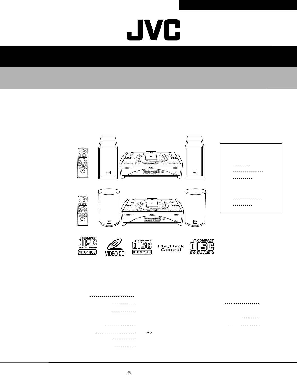
COMPACT COMPONENT SYSTEM
FS-SD58V
FS-SD78V / FS-SD98V
Contents
REMOTE CONTROL
DIMMER SLEEP
FM MODE
DISPLAY DOOR SLIDE
MPX
TONE
CLOCK
AHB PRO
CONTROL
/
TIMER
PLAY MODE REPEAT CANCEL
HIGHLIGHT
VIDEO INTRO STILL
PBC ON
/
OFF
ON SCREEN
VCD NUMBER
UP
NEXTPREV
SELECT
SET
DOWN
VCD NUMBER
FADE MUTING
CD
MD / AUX
FM / AM
VOLUME
CA-SD58V
REMOTE CONTROL
DIMMER SLEEP
FM MODE
DISPLAY DOOR SLIDE
MPX
TONE
CLOCK
AHB PRO
CONTROL
/
TIMER
PLAY MODE REPEAT CANCEL
HIGHLIGHT
VIDEO INTRO STILL
PBC ON
/
OFF
ON SCREEN
VCD NUMBER
UP
NEXTPREV
SELECT
SET
DOWN
VCD NUMBER
FADE MUTING
CD
MD / AUX
FM / AM
VOLUME
SP-SD78V, SD98V SP-SD78V, SD98V
CA-SD78V, CA-SD98V
These models are different only speaker systems.
FS-SD78V and FS-SD98V are different only speaker cabinet.
These models not have adjustment.
NTSC / PAL COMPATIBILITY
NTSC / PAL COMPATIBILITY
Area Suffix
FS-SD58V
UB
UF
SP-SD58VSP-SD58V
US
FS-SD78V / FS-SD98V
UF
US
Hong Kong
China
Singapore
China
Singapore
Safety Precautions
Important for laser products
Preventing static electricity
Dismantling and assembling
the traverse unit
Disassembly method
Maintenance of laser pickup
Replacement of laser pickup
This service manual is printed on 100% recycled paper.
COPYRIGHT 2000 VICTOR COMPANY OF JAPAN, LTD.
1-2
1-3
1-4
1-5
1-6 14
1-15
1-15
Flow of functional operation
unit TOC read
Method of connecting
treatment device wire
Description of major ICs
1-16
1-17
1-18
No.20882
Nov. 2000
Page 2

FS-SD58V/FS-SD78V/FS-SD98V
1. This design of this product contains special hardware and many circuits and components specially
for safety purposes. For continued protection, no changes should be made to the original design
unless authorized in writing by the manufacturer. Replacement parts must be identical to those
used in the original circuits. Services should be performed by qualified personnel only.
2. Alterations of the design or circuitry of the product should not be made. Any design alterations of
the product should not be made. Any design alterations or additions will void the manufacturer`s
warranty and will further relieve the manufacture of responsibility for personal injury or property
damage resulting therefrom.
3. Many electrical and mechanical parts in the products have special safety-related characteristics.
These characteristics are often not evident from visual inspection nor can the protection afforded
by them necessarily be obtained by using replacement components rated for higher voltage,
wattage, etc. Replacement parts which have these special safety characteristics are identified in
the Parts List of Service Manual. Electrical components having such features are identified by
shading on the schematics and by ( ) on the Parts List in the Service Manual. The use of a
substitute replacement which does not have the same safety characteristics as the recommended
replacement parts shown in the Parts List of Service Manual may create shock, fire, or other
hazards.
4. The leads in the products are routed and dressed with ties, clamps, tubings, barriers and the
like to be separated from live parts, high temperature parts, moving parts and/or sharp edges
for the prevention of electric shock and fire hazard. When service is required, the original lead
routing and dress should be observed, and it should be confirmed that they have been returned
to normal, after re-assembling.
5. Leakage currnet check (Electrical shock hazard testing)
After re-assembling the product, always perform an isolation check on the exposed metal parts
of the product (antenna terminals, knobs, metal cabinet, screw heads, headphone jack, control
shafts, etc.) to be sure the product is safe to operate without danger of electrical shock.
Do not use a line isolation transformer during this check.
Plug the AC line cord directly into the AC outlet. Using a "Leakage Current Tester", measure
the leakage current from each exposed metal parts of the cabinet , particularly any exposed
metal part having a return path to the chassis, to a known good earth ground. Any leakage
current must not exceed 0.5mA AC (r.m.s.)
Alternate check method
Plug the AC line cord directly into the AC outlet. Use an AC voltmeter having, 1,000 ohms
per volt or more sensitivity in the following manner. Connect a 1,500 10W resistor paralleled by
a 0.15 F AC-type capacitor between an exposed
metal part and a known good earth ground.
Measure the AC voltage across the resistor with the
AC voltmeter.
AC VOLTMETER
(Having 1000
ohms/volts,
or more sensitivity)
Move the resistor connection to eachexposed metal
part, particularly any exposed metal part having a
return path to the chassis, and meausre the AC
voltage across the resistor. Now, reverse the plug in
the AC outlet and repeat each measurement. voltage
measured Any must not exceed 0.75 V AC (r.m.s.).
0.15 F AC TYPE
1500 10W
Place this
probe on
each exposed
metal part.
This corresponds to 0.5 mA AC (r.m.s.).
Good earth ground
1-2
1. This equipment has been designed and manufactured to meet international safety standards.
2. It is the legal responsibility of the repairer to ensure that these safety standards are maintained.
3. Repairs must be made in accordance with the relevant safety standards.
4. It is essential that safety critical components are replaced by approved parts.
5. If mains voltage selector is provided, check setting for local voltage.
!
Burrs formed during molding may be left over on some parts of the chassis. Therefore,
pay attention to such burrs in the case of preforming repair of this system.
Page 3
Important for Laser Products
1.CLASS 1 LASER PRODUCT
2.DANGER : Invisible laser radiation when open and inter
lock failed or defeated. Avoid direct exposure to beam.
3.CAUTION : There are no serviceable parts inside the
Laser Unit. Do not disassemble the Laser Unit. Replace
the complete Laser Unit if it malfunctions.
4.CAUTION : The compact disc player uses invisible
laserradiation and is equipped with safety switches
whichprevent emission of radiation when the drawer is
open and the safety interlocks have failed or are de
feated. It is dangerous to defeat the safety switches.
5.CAUTION : If safety switches malfunction, the laser is able
to function.
6.CAUTION : Use of controls, adjustments or performance of
procedures other than those specified herein may result in
hazardous radiation exposure.
VARNING : Osynlig laserstrålning är denna del är öppnad
och spårren är urkopplad. Betrakta ej strålen.
VARO : Avattaessa ja suojalukitus ohitettaessa olet
alttiina näkymättömälle lasersäteilylle.Älä katso
säteeseen.
ADVARSEL : Usynlig laserstråling ved åbning , når
sikkerhedsafbrydere er ude af funktion. Undgå
udsættelse for stråling.
ADVARSEL : Usynlig laserstråling ved åpning,når
sikkerhetsbryteren er avslott. unngå utsettelse
for stråling.
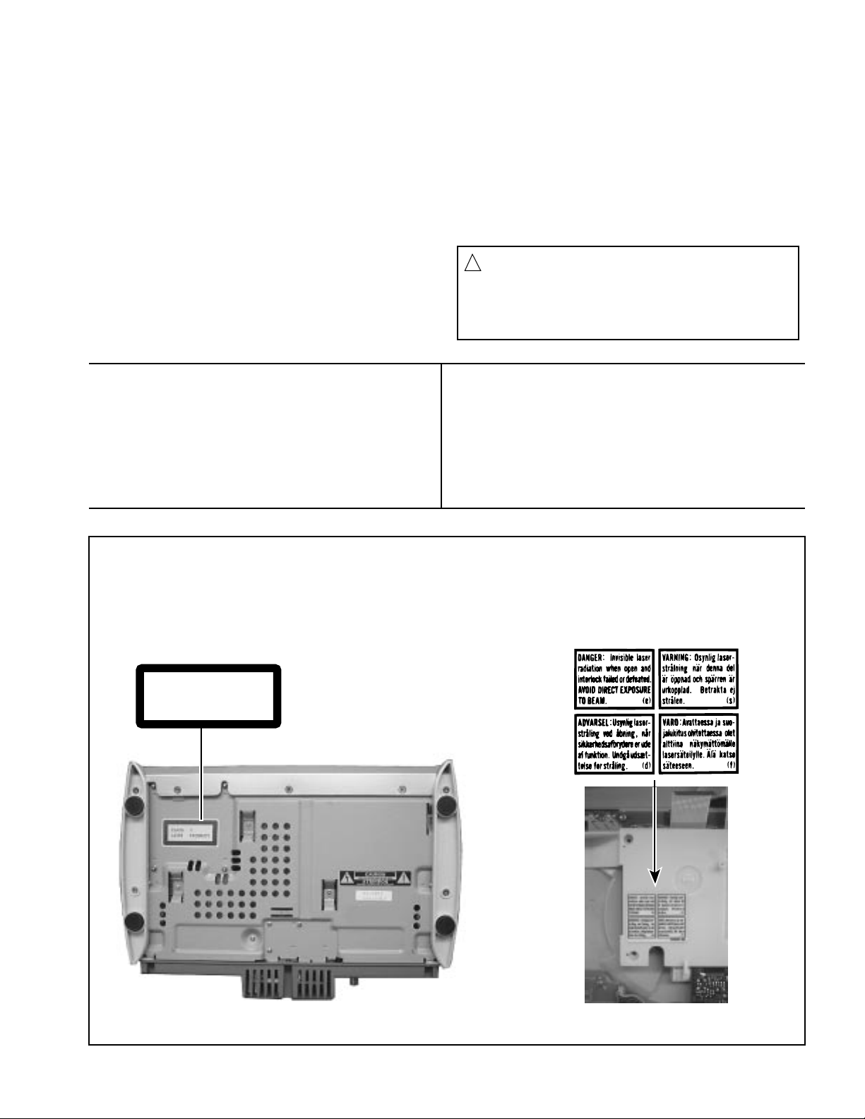
REPRODUCTION AND POSITION OF LABELS
WARNING LABEL
CLASS 1
LASER PRODUCT
!
CAUTION
Please use enough caution not to
see the beam directly or touch it
in case of an adjustment or operation
check.
FS-SD58V/FS-SD78V/FS-SD98V
1-3
Page 4
FS-SD58V/FS-SD78V/FS-SD98V
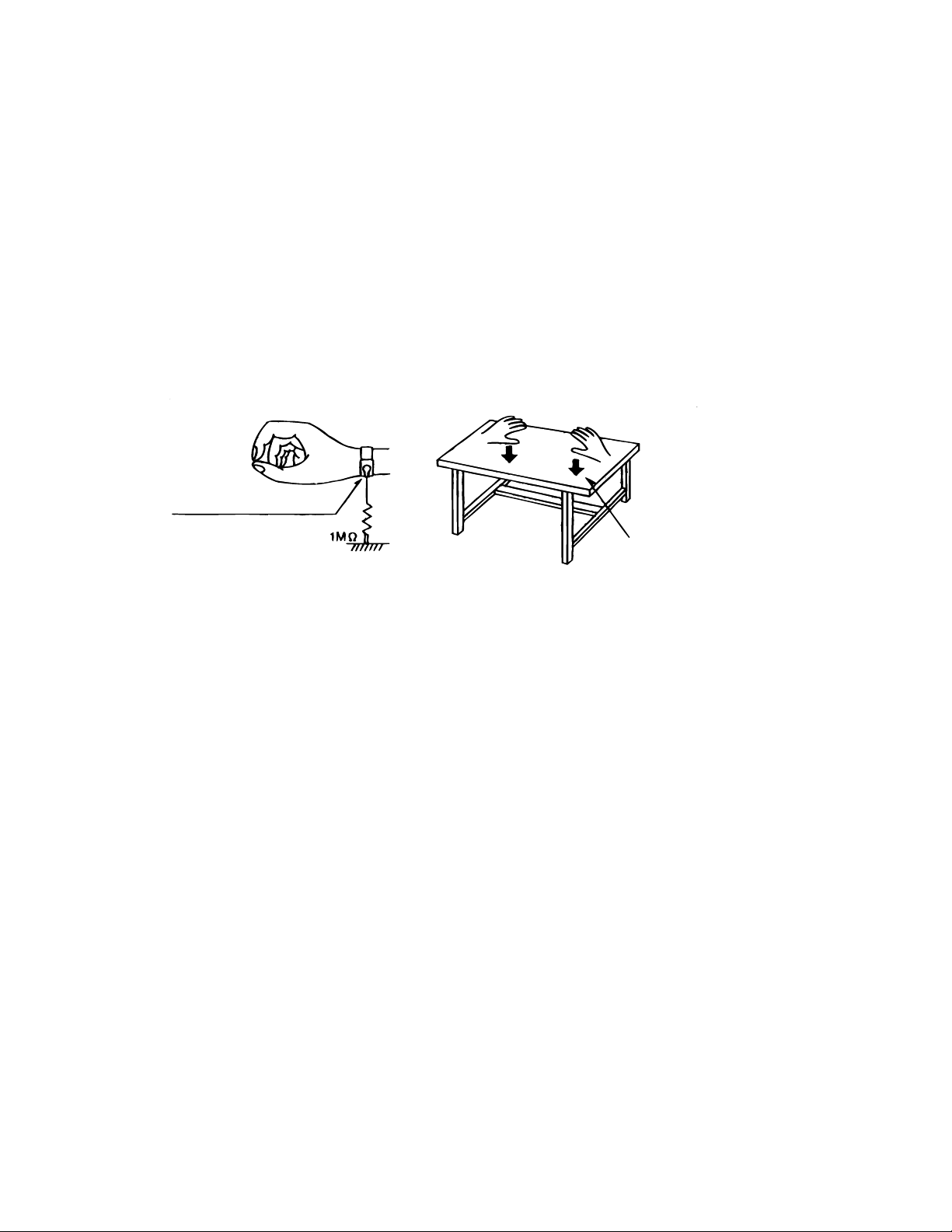
Preventing static electricity
Electrostatic discharge (ESD), which occurs when static electricity stored in the body, fabric, etc. is discharged,
can destroy the laser diode in the traverse unit (optical pickup). Take care to prevent this when performing repairs.
1.1. Grounding to prevent damage by static electricity
Static electricity in the work area can destroy the optical pickup (laser diode) in devices such as DVD players.
Be careful to use proper grounding in the area where repairs are being performed.
1.1.1. Ground the workbench
1. Ground the workbench by laying conductive material (such as a conductive sheet) or an iron plate over
it before placing the traverse unit (optical pickup) on it.
1.1.2. Ground yourself
1. Use an anti-static wrist strap to release any static electricity built up in your body.
(caption)
Anti-static wrist strap
Conductive material
(conductive sheet) or iron plate
1.1.3. Handling the optical pickup
1. In order to maintain quality during transport and before installation, both sides of the laser diode on the
replacement optical pickup are shorted. After replacement, return the shorted parts to their original condition.
(Refer to the text.)
2. Do not use a tester to check the condition of the laser diode in the optical pickup. The tester's internal power
source can easily destroy the laser diode.
1.2. Handling the traverse unit (optical pickup)
1. Do not subject the traverse unit (optical pickup) to strong shocks, as it is a sensitive, complex unit.
2. Cut off the shorted part of the flexible cable using nippers, etc. after replacing the optical pickup. For specific
details, refer to the replacement procedure in the text. Remove the anti-static pin when replacing the traverse
unit. Be careful not to take too long a time when attaching it to the connector.
3. Handle the flexible cable carefully as it may break when subjected to strong force.
4. It is not possible to adjust the semi-fixed resistor that adjusts the laser power. Do not turn it
1-4
Page 5
FS-SD58V/FS-SD78V/FS-SD98V
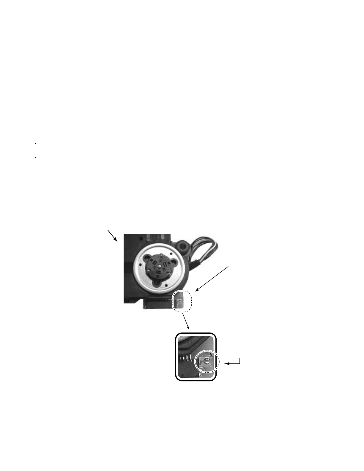
Dismantling and assembling the traverse unit
Notice regarding replacement of optical pickup
Electrostatic discharge (ESD), which occurs when static electricity stored in the body, fabric, etc. is discharged,
can destroy the laser diode in the traverse unit (optical pickup). Take care to prevent this when performing
repairs to the optical pickup or connected devices.
1. Do not touch the area around the laser diode and actuator.
2. Do not check the laser diode using a tester, as the diode may easily be destroyed.
3. It is recommended that you use a grounded soldering iron when shorting or removing the laser diode.
Recommended soldering iron: HAKKO ESD-compatible product
4. Solder the land on the optical pickup's flexible cable.
Note : Short the land after shorting the terminal on the flexible cable using a clip, etc., when using an
ungrounded soldering iron.
Note : After shorting the laser diode according to the procedure above, remove the solder according
to the text explanation.
Laser pick-up unit
KSM-770ABA
Shorting
Short circuit land
1-5
Page 6
FS-SD58V/FS-SD78V/FS-SD98V
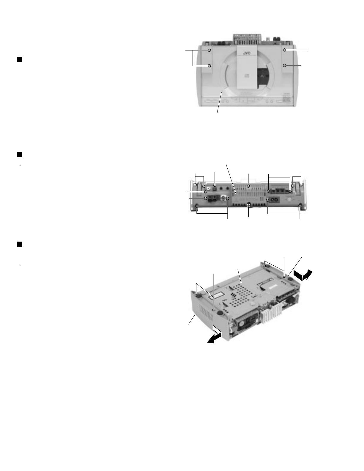
Disassembly method
<Main body>
Removing the CD door (See Fig.1)
1.
Remove the four screws A attaching the CD door on
the upper side of the body.
Removing the rear cover (See Fig.2)
Piro to performing the following procedure, remove
the CD door.
1.
Remove the ten screws B and the five screws C
attaching the rear cover on the back of the body.
B
C
CD door
Rear cover
B
Fig.1
C
B
AA
C
Removing the right and left covers
(See Fig.3)
Prior to performing the following procedure, remove
the CD door, the rear cover.
1.
Remove the four screws D attaching the side covers
on the bottom of the body.
2.
Move the left cover backward and remove outward.
Also remove the right cover in the same way.
Left cover
D
B
Bottom
B
Fig.2
Fig.3
Right cover
D
B
1-6
Page 7
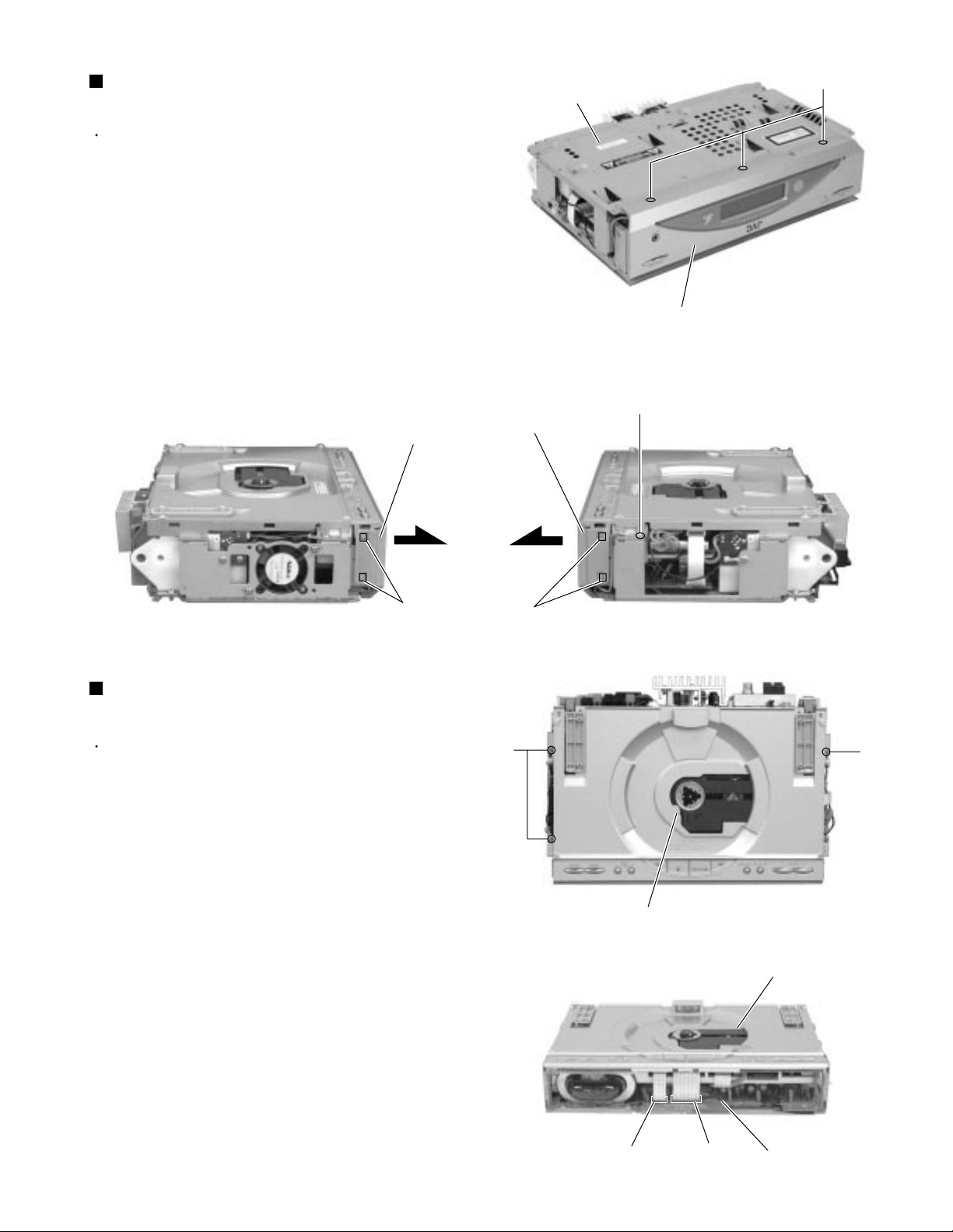
FS-SD58V/FS-SD78V/FS-SD98V
Removing the front panel assembly
(See Fig.4 to 6)
Prior to performing the following procedure, remove
the CD door, the rear cover and the side covers.
1.
Remove the three screws E on the bottom of the
body.
2.
Release two joints a and two joints b on both sides
of the body using a screwdriver and remove the front
panel assembly toward the front.
If necessary, remove the screw F which retains the
wire extending from the front panel assembly.
Left side
Front panel assembly
Bottom
Front panel assembly
Front panel assembly
E
Fig.4
F
Right side
Joints a
Removing the CD mechanism base
assembly (See Fig.7 to 14)
Prior to performing the following procedure, remove
the CD door, the rear cover, the side covers and the
front panel assembly.
1.
Disconnect the card wire from connector CN104 and
CN105 of the main board in the front part of the
body. Disconnect the card wire from CN101 of the
main board on the right side, and the wire from
CN705 of the CD mechanism base assembly
respectively.
2.
Remove the four screws F attaching the CD
mechanism base assembly on the upper side of the
body. Remove the screw I attaching the earth
terminal on the right side.
Joints b
F
CD door
Fig.6Fig.5
F
Fig.7
CD mechanism base assembly
CN104
CN105
Fig.8
Main bard
1-7
Page 8
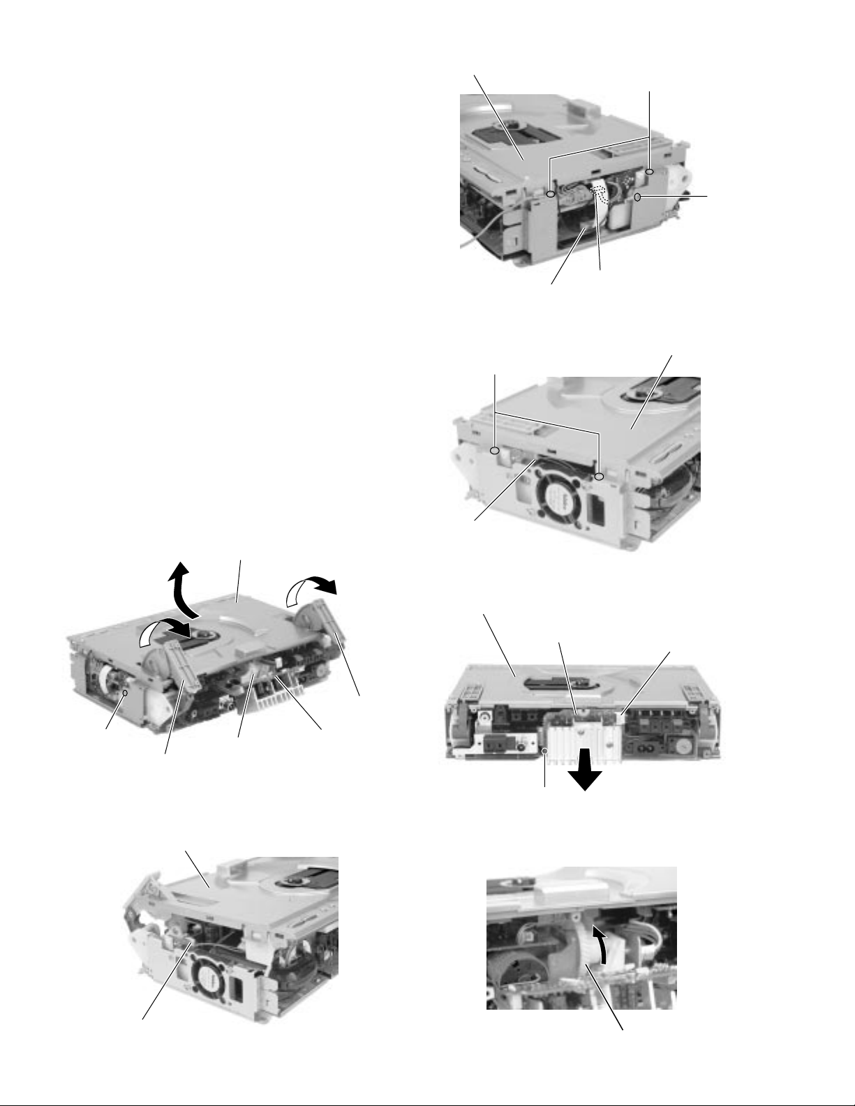
FS-SD58V/FS-SD78V/FS-SD98V
3.
Remove the screw G attaching the heat sink board
on the back of the body. Disconnect the wire from
connector CN301 and pull the heat sink board fully
outward.
4.
Raise the right and left door arms by turning the gear
a in the rear of the heat sink board.
5.
After the CD mechanism base assembly is detached
from the door arms, pull the CD mechanism base
assembly toward the front and disconnect the wire
from connector CN804 on the left side of the door
arm board.
6.
Pull out the CD mechanism base assembly toward
the front.
CD mechanism base assembly
F
I
CN705
Main board
CN101
Fig.9
CD mechanism base assembly
F
CD mechanism base assembly
I
Door arm
CD mechanism base assembly
Gear a
Fig.12
Door arm
Heat sink board
CN804
Fig.10
CD mechanism base assembly
Heat sink board
G
Fig.11
CN301
Door arm board (L)
1-8
CN804
Fig.14
Gear a
Fig.13
Page 9
FS-SD58V/FS-SD78V/FS-SD98V
Removing the door arm assembly / the
door arm board (R) and (L)
(See Fig.15 to 20)
Prior to performing the following procedure, remove
the rear cover, the side covers, the front panel
assembly and the CD mechanism base assembly.
1.
In case that the upper parts of the door arms
attached to the CD door are not level, let down them
to the level position by turning the gear a in the
direction of the arrow.
ATTENTION:
2.
Remove the four screws H on the upper side and
the one screw I on the left side of the body.
3.
Remove the four screws J attaching the door arm
board (L) and (R) on both sides of the door arm
assembly.
When the door arms incline, the door
arm assembly and the door arm board
(R) and (L) may not be removed.
Door arm
Door arm
Door arm board (L)
Fan motor
Fig.15
Door arms (Attached to the CD door)
Door arm board (R)
Door arm assembly
H
Fig.17
J
Door arm assembly
Fig.16
Door arm assembly
Fig.18
J
Door arm board (R)
H
J
Door arm board (L)
I
J
Fig.19
Fig.20
1-9
Page 10
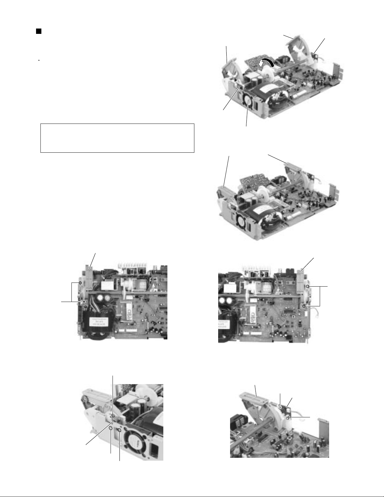
FS-SD58V/FS-SD78V/FS-SD98V
Removing the power amplifier board
(See Fig.21 and 22)
Prior to performing the following procedure, remove
the CD mechanism base assembly.
1.
Disconnect the wires from connector CN102 and
CN193 on the main board and release them from the
cord stopper respectively.
2.
Remove the two screws K and the two screws L
attaching the heat sink and the power amplifier
board.
Removing the transformer assembly
(See Fig.21)
Prior to performing the following procedure, remove
the CD mechanism base assembly.
1.
Disconnect the wires from connector CN191 and
CN192 on the main board and release them from the
cord stopper respectively.
Door arm assembly
CN191
Cord stopper
M
Cord stopper
Transformer assembly
Heat sink board
CN193
M
CN192
CN181
Fig.21
CN106
CN102
Heat sink board
Cord
stopper
Main board
Cord stopper
2.
Remove the four screws M attaching the transformer
assembly.
Removing the gear motor assembly
(See Fig.23 and 24)
Prior to performing the following procedure, remove
the CD mechanism base assembly and the door arm
assembly.
1.
Disconnect the wires from connector CN106 on the
main board and release it from the cord stopper.
2.
Remove the three screws N attaching the gear
motor assembly. Remove the gear motor assembly
with the gear motor stopper.
3.
Remove the belt from the gear motor assembly.
4.
Remove the two screws O from the gear motor
assembly.
Heat sink
Gear motor stopper
L
N
N
Motor
K
Fig.22
Gear motor assembly
CN106
Fig.23
Cord stopper
1-10
O
Belt
Fig.24
Page 11
Removing the fan motor assembly
(See Fig.25 and 26)
Prior to performing the following procedure, remove
the CD mechanism base assembly.
1.
Disconnect the wires from connector CN181 on the
main board.
2.
Remove the two screws P on the left side of the
body. Move the fan motor assembly upward to
remove it from the base chassis.
3.
Remove the two screws Q and the fan motor from
the fan bracket.
Fan motor
P
FS-SD58V/FS-SD78V/FS-SD98V
Main bard
CN181
Fig.25
Q
Removing the main board (See Fig.27)
Prior to performing the following procedure, remove
the CD mechanism base assembly and the door arm
assembly.
To facilitate operation process, remove the gear
motor assembly before performing the following
procedure.
1.
Disconnect the wires from connector CN102, CN106,
CN191, CN192, CN193 and CN181 on the main
board.
2.
Remove the five screws R attaching the main board
with the cord clamp.
<Front panel assembly>
Removing the front panel board
(See Fig.28)
Prior to performing the following procedure, remove
the front panel assembly.
1.
Remove the seven screws S attaching the front
panel board inside the front panel assembly.
Fan bracket
CN191
R
S
Fan motor
R
CN106
CN193
CN192
R
Front panel assembly
Fig.26
Gear motor assembly
Main board
R
CN102
CN181
Fig.27
S
S
S
Fig.28
1-11
Page 12
FS-SD58V/FS-SD78V/FS-SD98V
<CD mechanism base assembly>
Prior to performing the following procedure, remove
the CD mechanism base assembly.
Removing the speaker terminal board
(See Fig.29)
1.
Remove the screws T attaching the speaker terminal
board on the underside of the CD mechanism base
assembly.
Removing the VCD CB assembly
(See Fig.30 to 33)
1.
Disconnect the card wire from connector CN711 on
the CD mechanism board attached to the CD
mechanism base.
2.
Disconnect the wires from connector CN102 and
CN103 on the VCD CB assembly.
CD mechanism board
VCD CB assembly
VCD CB assembly
Card wire
Speaker terminal board
T
CD mechanism cover
Fig.29
3.
Unjoint the six joints (f) with the VCD shield (L) and
the VCD shield (U). Remove the VCD shield (L) in
the direction of the arrow.
4.
Remove the VCD CB assembly from the VCD shield
(L).
VCD CB board
CD mechanism board
CN711
Fig.30
f
f
CN103
f
CN102
f
Fig.31
f
VCD shield (L)
f
f
1-12
VCD shield (L)
f
VCD shield (U)
f
Fig.32Fig.33
Page 13

FS-SD58V/FS-SD78V/FS-SD98V
Removing the CD mechanism board /
mechanism assembly (See Fig.34 to 38)
Prior to performing the following procedure, remove
the VCD CB assembly.
1.
Turn over the CD mechanism assembly and remove
the screw X which retains the wire extending from
the CD mechanism board.
2.
Remove the seven screws U attaching the CD
mechanism cover and the CD mechanism board.
3.
Disconnect the wire from connector CN703 and
CN706 on the CD mechanism board respectively.
4.
Turn back the CD mechanism assembly and detach
the CD mechanism cover while pulling the CD
mechanism assembly outward to release the two
joint tabs marked c.
5.
Disconnect the card wire from the connector of the
CD mechanism assembly inside the CD mechanism
cover. Disconnect the wire from CN605 on the CD
mechanism board. Pull the CD mechanism assembly
out of the three shaft of the CD mechanism cover.
CD mechanism board
CN706
U
CN703
X
U
CD mechanism assembly
CD mechanism cover
U
U
Fig.34
ATTENTION:
6.
Remove the CD mechanism board from the CD
mechanism cover.
When reassembling, confirm that the
cushion of the CD mechanism assembly
is reattached to the three shafts.
Shafts
CD mechanism cover
Joint c
CD mechanism cover
Cushion
CD mechanism assembly
Tab
CD mechanism cover
Fig.35
CD mechanism assembly
Joint c
Tab
Fig.36
Cushion
CD mechanism
cover
CD mechanism board
CD mechanism board
CN605
Fig.37Fig.38
1-13
Page 14

FS-SD58V/FS-SD78V/FS-SD98V
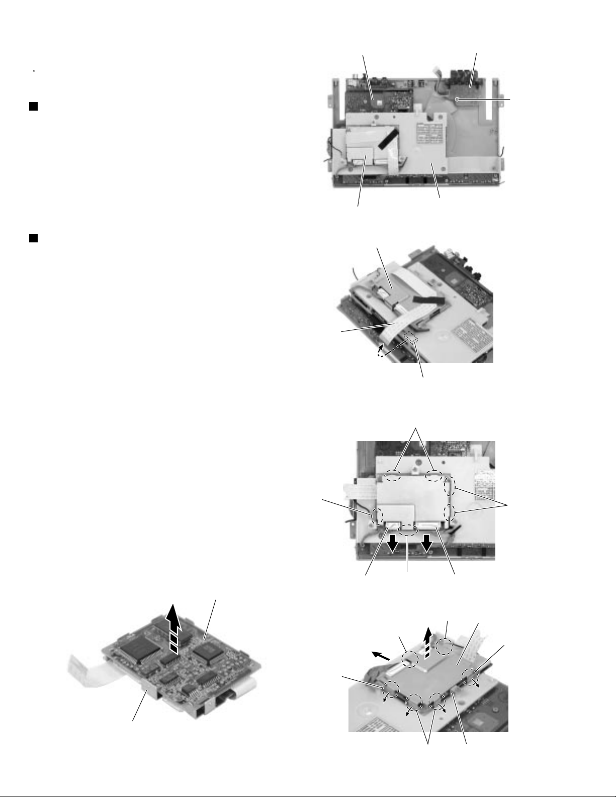
Removing the jack board (See Fig.39)
Prior to performing following procedure, remove the
CD mechanism board.
1.
Disconnect the wire from connector CN502 on the
jack board.
2.
Remove the two screws V attaching the jack board.
Removing the switch board (See Fig.39)
Prior to performing following procedure, remove the
CD mechanism board.
1.
Disconnect the wire from connector CN502 on the
jack board.
2.
Remove the six screws W attaching the switch
board.
Jack board
V
W
CD mechanism board
CN502
V
Fig.39
Tabs d
W
W
Switch board
Removing the LED board
(See Fig.40 and 41)
1.
Disconnect the wire from connector CN706 on the
CD mechanism board on the underside of the CD
mechanism base assembly.
2.
Push inward the two tabs d attaching the LED board
case and release them.
3.
Pull out the LED board from the LED board case.
Fig.40
LED board
Fig.41
LED board case
1-14
Page 15
FS-SD58V/FS-SD78V/FS-SD98V
Maintenance of laser pickup
(1) Cleaning the pick up lens
Before you replace the pick up, please try to
clean the lens with a alcohol soaked cotton
swab.
(2) Life of the laser diode
When the life of the laser diode has expired,
the following symptoms will appear.
1. The level of RF output (EFM output:amplitude
of eye pattern) will below.
Is the level of
RFOUT under
1.25V 0.22Vp-p?
YES
O.K
NO
Replace it.
Replacement of laser pickup
Turn off the power switch and,disconnect the
power cord from the ac outlet.
Replace the pickup with a normal one.(Refer
to "Pickup Removal" on the previous page)
Plug the power cord in,and turn the power on.
At this time,check that the laser emits for
about 3seconds and the objective lens moves
up and down.
Note: Do not observe the laser beam directly.
Play a disc.
Check the eye-pattern at TP1.
Finish.
(3) Semi-fixed resistor on the APC PC board The semi-fixed resistor on the APC printed circuit board which is
attached to the pickup is used to adjust the laser power.Since this adjustment should be performed to match the
characteristics of the whole optical block, do not touch the semi-fixed resistor.
If the laser power is lower than the specified value,the laser diode is almost worn out, and the laser pickup should
be replaced.
If the semi-fixed resistor is adjusted while the pickup is functioning normally,the laser pickup may be damaged
due to excessive current.
1-15
Page 16

FS-SD58V/FS-SD78V/FS-SD98V
Flow of functional operation until TOC read
Power ON
Play Key
Slider turns REST
SW ON.
Automatic tuning
of TE offset
Check Point
Confirm that the voltage at the pin4
of CN605 is "H"/"L"/"H".
Tracking error waveform at TOC reading
Approx.3sec
Tracking
servo
off states
Automatic measurement
of TE amplitude and
automatic tuning of
TE balance
VREF
pin 25 of
IC601(TE)
Approx
1.8V
Disc states
to rotate
Tracking
servo
on states
Disc to be
braked to stop
TOC reading
finishes
500mv/div
2ms/div
Fig.1
Laser ON
Detection of disc
Automatic tuning of
Focus offset
Automatic measurement of
Focus S-curve amplitude
Disc is rotated
Focus servo ON
(Tracking servo ON)
Automatic measurement of
Tracking error amplitude
Automatic tuning of
Tracking error balance
Check that the voltage at the
pin40 of IC603 is + 5V?
Confirm that the Focus error
S-cuve signal at the pin28 of
IC603 is approx.2Vp-p
Confirm that the signal from
pin24 IC603 is 0V as a
accelerated pulse during
approx.400ms.
Confirm the waveform of
the Tracking error signal.
at the pin 25 of IC601 (R6009)
(See fig-1)
1-16
Automatic tuning of
Focus error balance
Automatic tuning of
Focus error gain
Automatic tuning of
Tracking error gain
TOC reading
Play a disc
Confirm the eys-pattern
at the lead of TP602
Page 17

FS-SD58V/FS-SD78V/FS-SD98V
Method of connecting treatment device wire
When the KSM-770ABA mechanism is used, the expansion cable is used as follows.
EXTFSSD5-JIG
extension wire
QUQB12-0840CJ
8pin card wire
QUQB12-0940DJ
9pin card wire
QUQB12-1840DJ
18pin card wire
QUQB12-1640DJ
16pin card wire
First short-circuit the pickup circuit before removing the pickup.Then carry out the replacement.
Refer to "Dismantling and assembling the traverse unit" on page 1-5.
KSM-770ABA
Laser pick-up unit
Shorting
Short circuit land
1-17
Page 18
FS-SD58V/FS-SD78V/FS-SD98V
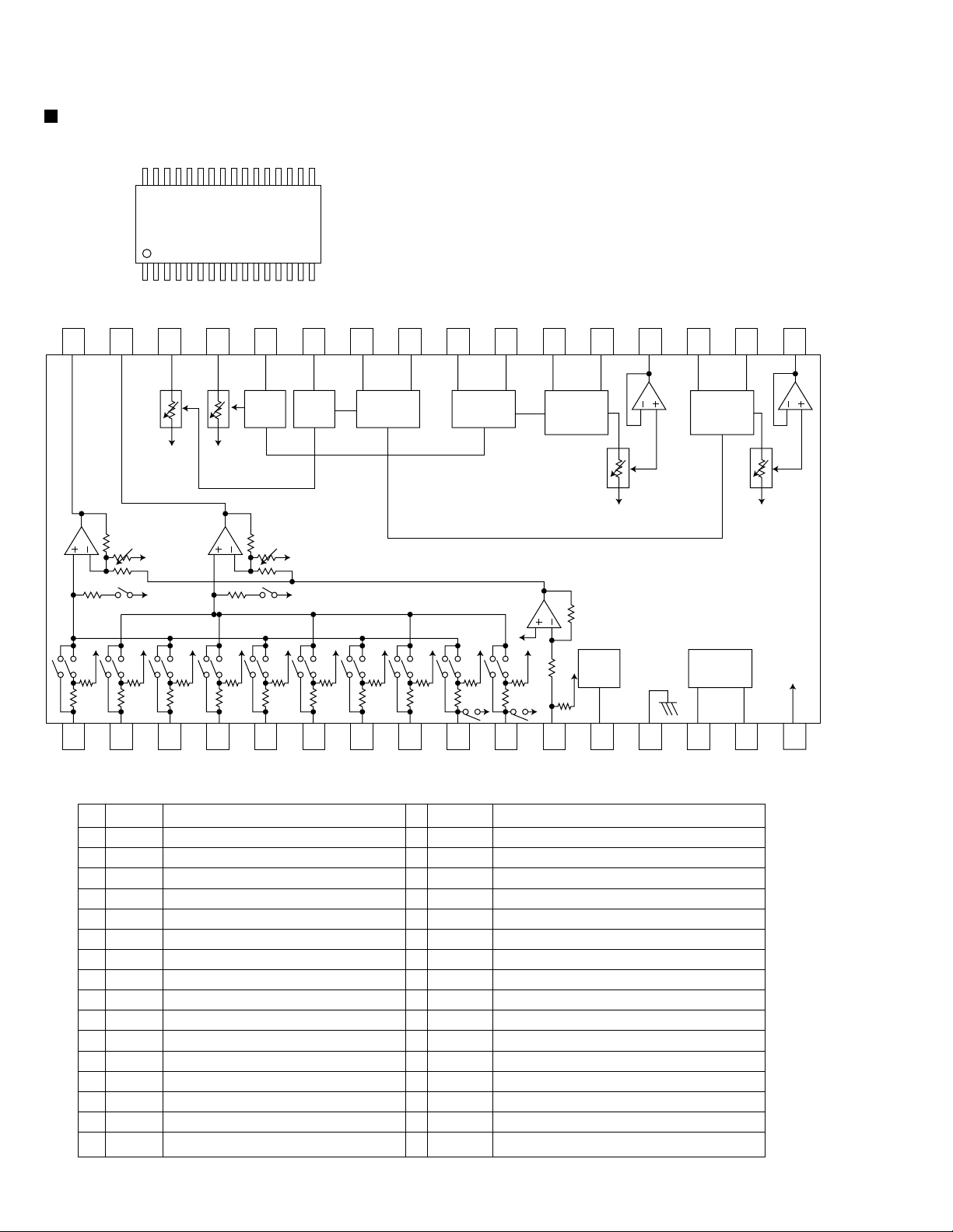
Description of major ICs
BD3861FS-X (IC501) : Audio sound control
1. Pin layout
32 18
117
2. Block diagram
32 31 30 29 28 27 26 25 24 23 22 21 20 19 18 17
0dB~
-70dB
Vcc/2 Vcc/2
Vcc/2
Vcc/2
25k
25k
12345678910111213141516
25k
25k
25k
25k
25k
25k
Treble1
f0=10kHz
25k
25k
Treble2
f0=10kHz
Vcc/2
Vcc/2
25k
25k
Middle2
f0=1kHz
25k
25k
25k
25k
Middle1
f0=1kHz
25k
25k
25k
25k
Bass1
f0=90Hz
12k
100k
0dB~
-59dB
24k
Vcc/2
Vcc/2
Bass2
f0=90Hz
0dB~
-59dB
Vcc/2
Vcc/2
Logic
3. Pin function
Pin
Symbol SymbolFunction Function
No.
1
2
3
4
5
6
7
8
9
10
11
12
13
14
15
16
A1
A2
B1
B2
C1
C2
D1
D2
E1
E2
MIC
FIL
GND
DATA
CLK
Vcc
CH1 input pin A
CH2 input pin A
CH1 input pin B
CH2 input pin B
CH1 input pin C
CH2 input pin C
CH1 input pin D
CH2 input pin D
CH1 input pin E
CH2 input pin E
Microphone input pin
Filter pin
Ground pin
Serial data latch receiving pin
Serial clock receiving pin
Power supply pin
17
18
BASS21
19
BASS22
20
21
BASS11
22
BASS12
23
24
25
26
27
28
29
30
31
32
OUT2
OUT1
MID11
MID12
MID21
MID22
TRE2
TRE1
VOL1
VOL2
GOUT2
GOUT1
CH2 output pin
CH2 bass filter setting pin
CH2 bass filter setting pin
CH1 output pin
CH1 bass filter setting pin
CH1 bass filter setting pin
CH1 middle filter setting pin
CH1 middle filter setting pin
CH2 middle filter setting pin
CH2 middle filter setting pin
CH2 treble filter setting pin
CH1 treble filter setting pin
CH1 input volume input pin
CH2 input volume input pin
CH2 input gain output pin
CH1 input gain output pin
1-18
Page 19

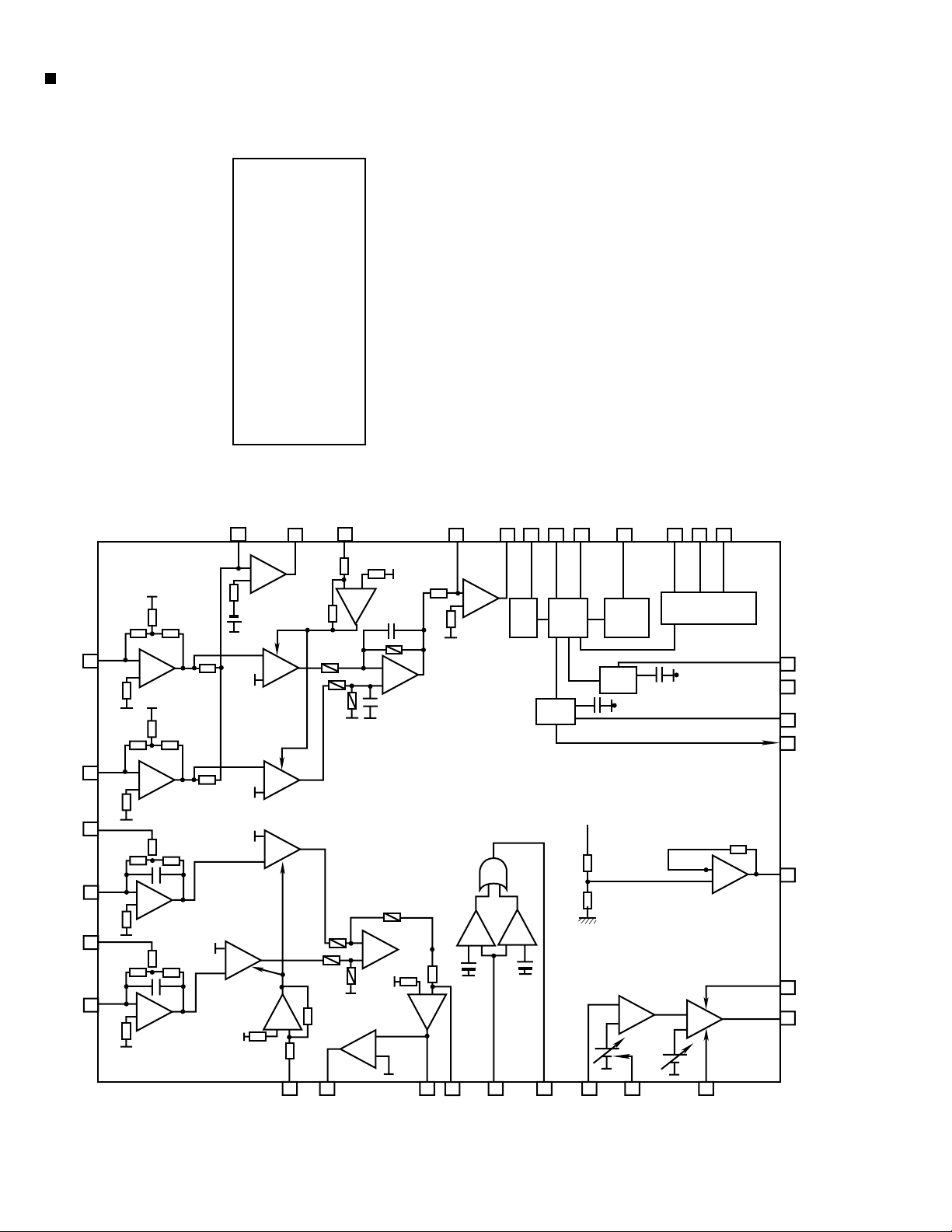
LA6541-X(IC602) : Servo Driver
1. Pin Layout & Block Diagram
FS-SD58V/FS-SD78V/FS-SD98V
Vcc Vref Vin4 Vg4 Vo8 Vo7
24 23
22
21
20
19
11k
Vcc
Gnd
Vo6 Vo5 Vg3 Vin3 Cd Res
18
17 16
ohm
- +
- +
Level
shift
Level
shift
B T L
driver
B T L
driver
B T L
driver
B T L
driver
Level
shift
Level
shift
11k
ohm
1
2
Vcc Mute Vin1 Vg1 Vo1 Vo2 Vo3 Vo4 Vg2 Vin2 Reg
3456
Gnd
7 8 9101112
2. Pin functions
Pin
Symbol Function
No.
1
10
11
12
13
14
15
16
17
18
19
20
21
22
23
24
2
3
4
5
6
7
8
9
Vcc
Mute
Vin1
Vg1
Vo1
Vo2
Vo3
Vo4
Vg2
Vin2
Reg Out
Reg In
Res
Cd
Vin3
Vg3
Vo5
Vo6
Vo7
Vo8
Vg4
Vin4
Vref
Vcc
Power supply (Shorted to pin 24)
All BTL amplifier outputs ON/OFF
BTL AMP 1 input pin
BTL AMP 1 input pin (For gain adjustment)
BTL AMP 1 input pin (Non inverting side)
BTL AMP 1 input pin (Inverting side)
BTL AMP 2 input pin (Inverting side)
BTL AMP 2 input pin (Non inverting side)
BTL AMP 2 input pin (For gain adjustment)
BTL AMP 2 input pin
External transistor collector (PNP) connection. 5V power supply output
External transistor (PNP) base connection
Reset output
Reset output delay time setting (Capacitor connected externally)
BTL AMP 3 input pin
BTL AMP 3 input pin (For gain adjustment)
BTL AMP 3 output pin (Non inverting side)
BTL AMP 3 output pin (Inverting side)
BTL AMP 4 output pin (Inverting side)
BTL AMP 4 output pin (Non inverting side)
BTL AMP 4 output pin (For gain adjustment)
BTL AMP 4 output pin
Level shift circuit's reference voltage application
Power supply (Shorted to pin 1)
15
14
13
11k
ohm
RESET
Regulator
11k
ohm
Reg
out
In
1-19
Page 20

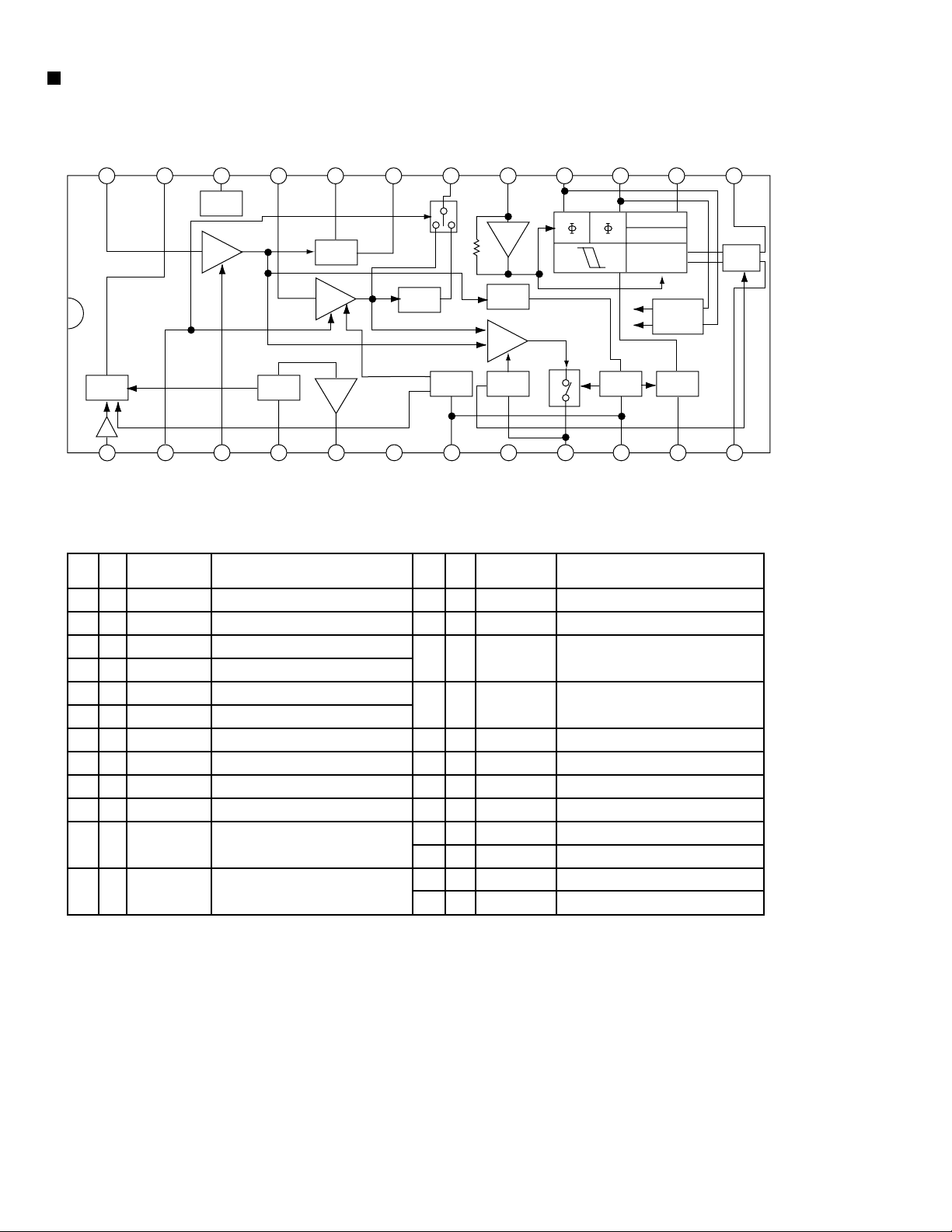
FS-SD58V/FS-SD78V/FS-SD98V
LA4905 (IC301) : 2ch BTL power IC
1. Pinlayput
123
2. Block diagram
STBY
D.C
PRE GND
IN 1
21
20
2
3
Standby SW
Ripple
filter
Input amplifier
Vcc Vcc(SW)
10
Switching
regulator block
H.L.S.
ABCD
H.L.S. :
Higher
Level signal
selector
Nonlinear/output stage
CH 1
11
Amplifier output stage
SW
drive
8
9
SW B
15
SW E
14
SW OUT1
12
SW OUT2
13
SW GND
16
A
+OUT 1
7
PWR GND 1
5
B
1-20
BEEP
IN 2
ON TIME
4
1
23
BEEP
amplifier
Input amplifier
ON MUTE
muting circuit
Power supply/ground shorting
protection circuit
Overvoltage/thermal protection
circuit
CH 2
Nonlinear amplifier/output stage
Pop noise
prevention circuit
-OUT 1
6
C
D
18
19
17
22
-OUT 2
PWR GND 2
+OUT 2
N.C.
Page 21

LC72136N (IC2) : PLL Frequency synthesizer
1. Pin layout
FM/AM
CLOCK
FM/ST/VCO
AM/FM
2. Block
XT
CE
DI
DO
SDIN
1
2
3
4
5
6
7
8
9
10
11
22
21
20
19
18
17
16
15
14
13
12
XT
GND
LPFOUT
LPFIN
PD
VCC
FMIN
AMIN
IFCONT
IFIN
FS-SD58V/FS-SD78V/FS-SD98V
3. Function
Pin
Symbol
No.
1
FM/AM
2
3
4
CLOCK
5
6
FM/ST/VCO
7
AM/FM
8
9
10
11
1
22
16
15
3
4
5
6
17
21
XT
CE
DI
DO
LW
MW
SDIN
Reference
Driver
Swallow Counter
1/2
C
2
B
I/F
Powe r
on
Reset
Function
I/O
X'tal oscillator connect (75kHz)
I
LOW:FM mode
O
When data output/input for 4pin(input) and
I
Swallow Counter
1/16,1/17 4bit
1/16,1/17 4bit
12bit
Programmable
Drivers
Data Shift Register & Latch
7821113
6pin(output): H
Input for receive the serial data from
I
controller
Sync signal input use
I
Data output for Controller
O
Output port
"Low": MW mode
O
Open state after the power on reset
O
Input/output port
I/O
Input/output port
I/O
Data input/output
I/O
Phase
Detector
Charge Pump
Unlock
Detector
Universal
Counter
Pin
No.
12
13
14
15
16
17
18
19
20
21
22
Symbol
IFIN
IFCONT
AMIN
FMIN
VCC
PD
LPFIN
LPFOUT
GND
XT
18
19
20
12
I/O
Function
IF counter signal input
I
IF signal output
O
Not use
-
AM Local OSC signal output
I
FM Local OSC signal input
I
Power suplly(VDD=4.5-5.5V)
When power ON:Reset circuit move
PLL charge pump output(H: Local OSC
O
frequency Height than Reference frequency.
L: Low Agreement: Height impedance)
Input for active lowpassfilter of PLL
I
Output for active lowpassfilter of PLL
O
Connected to GND
X'tal oscillator(75KHz)
I
1-21
Page 22

FS-SD58V/FS-SD78V/FS-SD98V
UPD780024AGKB09 (IC701) : CPU
1. Pin layout
64 ~ 49
1
48
2. Block diagram
~
16
17 ~ 32
16-bit TIMER/
EVENT COUNTER
8-bit TIMER/
EVENT COUNTER50
8-bit TIMER/
EVENT COUNTER51
WATCHDOG TIMER
WATCH TIMER
SERIAL
INTERFACE30
33
~
PORT0
PORT1
PORT2
PORT3
78K/0
CPU
CORE
ROM
(32K
BYTE)
PORT4
PORT5
SERIAL
INTERFACE31
UART0
A/D CONVERTER
INTERRUPT
CONTROL
BUZZER OUTPUT
CLOCK OUTPUT
CONTROL
RAM
(1024
BYTE)
VDD0 VDD1 Vss0 Vss1 IC
PORT6
PORT7
EXTERNAL
ACCESS
SYSTEM
CONTROL
1-22
Page 23

FS-SD58V/FS-SD78V/FS-SD98V
3. Pin function
Pin
No.
10
11
12
13
14
15
16
17
18
19
20
21
22
23
24
25
26
27
28
29
30
31
32
33
34
35
36
37
38
39
40
41
42
43
44
45
46
47
48
49
50
51
52
53
54
55
56
57
58
59
60
61
62
63
64
1
2
3
4
5
6
7
8
9
Symbol I/O Function
MT0
MT1
MTS
BLCTL
AHB
SMUTE
TUST
CDLED
VSS0
VDD0
MPX
RDSDI
DRMUTE
SCD
TUDATA(I)
TUDATA(O)
TUCK
SUBQ
XRST
SQCK
MLD
M DATA
MCLK
VDD1
AVSS
S TAT
REST
KEY1
KEY2
KEY3
SAFETY
LDCK
VERSION
AVREF
AVDD
RESET
XT2
XT1
IC
X2
X1
VSS1
REM
RDSCK
XKILL
BEAT
BUP
+BCTL
V DATA
VCLK
DOOR1
DOOR2
DOOR3
LOMUTE
RS
E
D84
D85
D86
D87
DIMMER
POUT
FTU
FCD
O
CD door motor control signal 0 output
O
CD door motor control signal 1 output
O
Motor speed control output (L:Normal, H:Slow)
O
Back light power supply control output
O
AHB ON/OFF control signal output (L:ON, H:OFF)
O
System mute control signal output
O
Tuner control strove output
O
CD LED control signal output (L:OFF, H:ON)
-
Ground at port section
-
Power supply at port section
I
Stereo indicator control signal input (L:Stereo)
I
RDS data input
O
Driver mute output
I
Voltage detection for safety of CD
I
Tuner control data input
O
Tuner control data output
O
Tuner control clock output
I
CD control Q code input
O
CD control reset signal output
O
CD control Q code clock signal output
O
CD control command load signal output
O
CD control command data signal output
O
CD control command clock signal output
-
Power supply without port section
-
Ground of A/D converter
I
CD control status signal input
I
CD rest switch detection signal input
I
Main body top section tact switch detection signal input
I
Main body top section tact switch detection signal input
I
Main body front section tact switch detection signal input
I
Voltage detection for safety
I
CD door motor lock detection signal input
I
Version detection
I
Reference voltage input for A/D converter
-
Analog power supply for A/D converter
I
System reset signal input
-
Sub clock
I
Sub clock signal input 32.768kHz
I
Connect to VSS0 or VSS1
-
Main clock
I
Main clock signal input 4.19MHz
-
Ground without port section
I
Remote controller signal input
I
RDS clock signal input
O
Sub clock OSC control signal output
O
Main clock shift control signal output
I
Back up detection signal input
O
Power supply control at back up operating
O
BD3861FS (VOL & FUNC IC) control data signal output
O
BD3861FS (VOL & FUNC IC) control clock signal output
I
Cd door position detection switch input
I
CD door position detection switch input
I
CD door position detection switch input
O
LINE OUT muting control signal output
O
LCD driver control resistor select signal output
O
LCD driver control enable signal output
O
LCD driver control data bus signal output
O
LCD driver control data bus signal output
O
LCD driver control data bus signal output
O
LCD driver control data bus signal output
O
Back light DIMMER control signal output
O
Power supply control signal output for amp section
O
Power supply control signal output for TUNER function
O
Power supply control signal output for CD function
UPD780024AGKB09
1-23
Page 24
FS-SD58V/FS-SD78V/FS-SD98V
AN8806SB-W(IC601) :RF&SERVO AMP
1.Pin layout
PD 1
LD 2
LDON 3
LDP 4
VCC 5
RF- 6
RF OUT 7
RF IN 8
C.AGC 9
ARF 10
C.ENV 11
C.EA 12
CS BDO 13
BDO 14
CS BRT 15
OFTR 16
/NRFDET 17
GND 18
2.Block diagram
36 PDAC
35 PDBD
34 PDF
33 PDE
32 PDER
31 PDFR
30 TBAL
29 FBAL
28 EF27 EF OUT
26 TE25 TE OUT
24 CROSS
23 TE BPF
22 VDET
21 LD OFF
20 VREF
19 ENV
6
29
728
27
910 17
8
11
12 19
+
- +
+
EQ
AGC
RF
DET
ENV CURCUIT
36
+
35
+
31
34
-
+
VCBA
-
+
VCBA
-
-
VCBA
+
+
OFTR
BDO
+
13
14
15
16
20
+
- +
32
33
+
-
VCBA
+
+ -
+
- +
21
2
+
-
24 25
30
23
26
22
14
3
1-24
Page 25

FS-SD58V/FS-SD78V/FS-SD98V
3. Pin function
Pin No.
1
2
3
4
5
6
7
8
9
10
11
12
13
14
15
16
17
18
19
20
21
22
23
24
25
26
27
28
29
30
31
32
33
34
35
36
symbol
/NRFDET
PD
LD
LD ON
LDP
VCC
RF-
RF OUT
RF IN
C.AGC
ARF
C.ENV
C.EA
CS BDO
BDO
CS BRT
OFTR
GND
ENV
VREF
LD OFF
VDET
TE BPF
CROSS
TE OUT
TE-
FE OUT
FE-
FBAL
TBAL
PDFR
PDER
PDF
PDE
PD BD
PD AC
I/O
I
APC amp . Input terminal
APC amp . Output terminal
O
LD ON/OFF control terminal
I
Connect to GND
-Power supply
-RF amp . Reversing input terminal
I
RFamp . Output terminal
O
AGC input terminal
I
AGC loop filter connection terminal
I/O
ARF output terminal
O
RF detection capacity connection terminal
I/O
HPF-amp capacity connection terminal
I/O
Capacity connection terminal for RF discernment side envelope detection
I/O
BDO output terminal
O
Capacity connection terminal for RF discernment side envelope detection
I/O
O
OFTR output terminal
RFDET output terminal
O
--
Connect to GND
O
3TENV output terminal
O
VREF output terminal
--
APC OFF control terminal
O
VDET output terminal
I
VDET input terminal
O
CROSS output terminal
O
TE amp . Output terminal
I
FE amp . Reversing input terminal
O
FE amp . output terminal
I
FE amp . Reversing input terminal
I
F.BAL control terminal
I
T.BAL control terminal
I/O
I-V amp conversion resistance adjustment terminal
I/O
I-V amp conversion resistance adjustment terminal
I
I-V amp input terminal
I-V amp input terminal
I
I
I-V amp input terminal
I
I-V amp input terminal
Function
AN8806SB-W
1-25
Page 26

FS-SD58V/FS-SD78V/FS-SD98V
MN35510(IC603):Digital servo & Digital signal processer
1. Terminal Layout
20 ~ 1
2.Block Diagram
LRCKIN(MSEL)
BCLK(SSEL)
SRDATAIN
(PSEL)
IOSEL
CLVS
CRC
BLKCK
CLDCK
SBCK
SUBC
DEMPH
RESY
FLAG6(RESY)
SSEL
SQCK
SUBQ
AVDD2
AVDD2
PCK
EFM
PLLF
DSLF
IREF
DRF
ARF
RSEL
PSEL
MLD
MCLK
MDATA
CK384(EFM)
VCOF
BYTCK
SMCK
FCLK
CSEL
MSEL
X2
X1
ÊSTAT
DIGITAL
DEEMPHSIS
SUB
CODE
BUFFER
DSL.
PLL
VCO
VCO
ITUNING
GENERATION
PITCH
CONTROL
21
~
40
41 ~ 60
8TIMES
OVER SAMPUNC
DIGITAL FILTER
EFM
DEMODULATION
SYNC
INTERPOLATION
SUBCODE
DEMODULATION
MICRO
COMPUTER
INTERFACE
CONVERTER
A/D
80
~
61
1BIT
DAC
LOGIC
S
16k
SRAM
CIRC
ERROR
CORRECTION
DEINTERLEVE
CLV
SERVO
INPUT
PEM
(R)
PEM
(L)
D/A
CONVERTER
OUTPUT
DIGITAL
AUDIO
INTERFASE
DIGITAL
AUDIO
INTERFASE
INTER POLATION
SOFT MUTING DIGITAL
ATTENUATION
PEAK DETECTIVE
AUTO CUE
PORT
SERVO
TIMING GENERATOR
AVSS1
AVDD1
OUTR
OUTL
FLAG
IPFLAG
TX
ECM
PC
LRCK
SRDATA
BCLK
DMUTE
TRKV
KICK
VREF
TRVSTR
ECS
TVD
TRD
FOD
TBAL
FBAL
TOFS
TES
/TLOCK
/FLOCK
PLAY
LDON
WVEL
SENSE
1-26
D
/
D
V
V
V
S
D
D
S
D
D
1
/
R
V
T
S
S
E
T
S
S
1
T
F
E
R
T
F
E
E
N
V
T
R
C
R
S
B
V
D
D
O
E
T
/
R
F
D
E
O
F
T
Page 27

FS-SD58V/FS-SD78V/FS-SD98V
3. Description
Pin
No.
1
2
3
4
5
6
7
8
9
10
11
12
13
14
15
16
17
18
19
20
21
22
23
24
25
26
27
28
29
30
31
32
33
34
35
36
37
38
39
40
symbol
BCLK
LRCK
SRDATA
DVDD1
DVSS1
TX
MCLK
MDATA
MLD
SENSE
FLOCK
TLOCK
BLKCK
SQCK
SUBQ
DMUTE
STATUS
RST
SMCK
PMCK
TRV
TVD
PC
ECM
ECS
KICK
TRD
FOD
VREF
FBAL
TBAL
FE
TE
RF ENV
VDET
OFT
TRCRS
RFDET
BDO
LDON
I/O
O
O
O
O
O
Description
Not used
Not used
Not used
I
Power supply (Digital)
I
Connected to GND
Digital audio interface output
Micom command clock signal input
I
(Data is latched at signal's rising point)
Micom command data input
I
I
Micom command load signal input
Sence signal output
O
Focus lock signal output Active :Low
O
Tracking lock signal output Active :Low
sub-code - block - clock signal output
O
I
Outside clock for sub-code Q resister input
Sub-code Q -code output
O
I
Connected to GND
Status signal
O
(CRC,CUE,CLVS,TTSTOP,ECLV,SQOK)
Reset signal input (L:Reset)
I
I
Not used
I
Not used
O
Traverse enforced output
O
Traverse drive output
I
Not used
Spindle motor drive signal (Enforced
O
mode output) 3-State
Spindle motor drive signal (Servo error
O
signal output)
Kick pulse output
O
Tracking drive output
O
O
Focus drive output
Reference voltage input pin for D/A
I
output block (TVD,FOD,FBA,TBAL)
Focus Balance adjust signal output
O
O
Tracking Balance adjust signal output
Focus error signal input(Analog input)
I
Tracking error signal input(Analog input)
I
I
RF envelope signal input(Analog input)
Vibration detect signal input(H:detect)
I
Off track signal input(H:off track)
I
Track cross signal input
I
RF detect signal input(L:detect)
I
BDO input pin(L:detect)
I
Laser ON signal output(H:on)
O
Pin
No.
41
42
43
44
45
46
47
48
49
50
51
52
53
54
55
56
57
58
59
60
61
62
63
64
65
66
67
68
69
70
71
72
73
74
75
76
77
78
79
80
symbol
TES
PLAY
WVEL
ARF
IREF
DRF
DSLF
PLLF
VCOF
AVDD2
AVSS2
EFM
PCK
PDO
SUBC
SBCK
VSS
XI
X2
VDD
BYTCK
CLDCK
FLAG
IPPLAG
FLAG
CLVS
CRC
DEMPH
RESY
IOSEL
TEST
AVDD1
OUT L
AVSS1
OUT R
RSEL
CSEL
PSEL
MSEL
SSEL
I/O
Tracking error shunt signal output(H:shunt)
O
I
Not used
I
Not used
I
RF signal input
Reference current input pin
I
Bias pin for DSL
I
I/O
Loop filter pin for DSL
Loop filter pin for PLL
I/O
I
Not used
I
Power supply(Analog)
Connected to GND(Analog)
Not used
II I
Not used
I
Not used
I
Not used
I
Not used
Connected to GND(for X'tal oscillation
I
circuit)
Input of 16.9344MHz X'tal oscillation circuit
I
Output of X'tal oscillation circuit
O
I
Power supply(for X'tal cscillation circuit)
I
Not used
I
Not used
I
Not used
I
Not used
I
Not used
I
Not used
I
Not used
Not used
I
Not used
III
pull up
pull up
Power supply(Digital)
Lch audio output
O
I
Connected to GND
Rch audio output
O
II
pull up
Connected to GND
I
Connected to GND
I
Connected to GND
I
Pull up
Description
MN35510
1-27
Page 28
FS-SD58V/FS-SD78V/FS-SD98V
TA2057N (IC1) : FM/AM IF AMP & Detector
1.Block Diagrams
FM
IF IN
24 23 22 21 20 19 18 17 16 15 14 13
AM
MIX
OUT Vstb QUAD FM OUT AM OUT MPX IN LPF 1 LPF 2 VCO L OUT
AM
IF IN
AM
MIX
123456789 1110 12
AM
RF IN
2.Pin Function
Pin
No.
I/O
1
I
2
3
4
5
6
7
8
9
10
11
12
AM S.SENS
FM S.SENS
-
AM OSC OUT
O
-
I
-
O
O
O
O
REG
FM
IF
S.SENSFMS.SENS
Symbol
AM RF
AM OSC
VCC
AGC
GND
IF OUT
TU IND
ST IND
Rch OUT
AMRF signal input
AM local oscillation circuit
AM local oscillation signal output
Power supply
AGC voltage input terminal
Connect to GND
IF REQ signal output to IC2
Indicator drive output when tuning
Stereo indicator output
"H"mono . "L"stereo
Output Rch
DECODE
TUN
LED
TUN
LED
VCO
DIVIDE
LEVEL
SW
IF
BUFF
IF REQ
SW
Lch OUT
O
O
O
O
MPX IN
I
AM OUT
O
FM OUT
O
FM QUAD
I
AM IF IN
I
-
AM MIX OUT
O
FM IF IN
I
AM
Symbol
VCO
LPF2
LPF1
Vst
/REQ
Output Lch
Voltage controlled terminal
When voltage of terminal is MONO
at "H" and ST at "L"
When voltage of terminal is AM at
"H" and FM at "L"
Multi plex signal input
AM detection signal output
FM detection signal output
Bypass to FMIF
Input of AMIF signal
Fixed voltage output terminal
Output terminal for AM mixer
Input of FMIF signal
FM
DET
AM
IF
AM
OSC
AM
OSCAMOSC
BUFF
OUT
Function Function
AM
DET
AGC
Vcc AGC GND IF OUT
Pin
No.
I/O
13
14
15
16
17
18
19
20
21
22
23
24
AM/FM
MONO
SW
ST
LED
ST
LED
MUTE
R OUTAM
1-28
Page 29

UPD780053GC-031(IC711):CD/VCD Control
1. Terminal layout
40 21
41
20
FS-SD58V/FS-SD78V/FS-SD98V
2Pin function
Pin
No.
1
2
3
4
5
6
7
8
9
10
11
12
13
14
15
16
17
18
19 32
33
34 39
40
41
42
43
44 59
60
61
62
63
64 66
67
68
69
70
71
72
73
74
75
76 78
79
80
VCDEMP
CDMRST
DRMUTE
60
61 80
Symbol I/O Function
MLD
M DATA
MCLK
AVSS
REST
XRST
A-REF1
SUBQ
NC
SQCK
KCMD
M S TAT
KCLK
OSOFF
MRDY
NC
SRDATA
SRCLK
NC
VSS1
NC
FCD
MREQ
VCDRST
NC
S TAT
HREC
HRDY
NC
V3S0
VDD1
X2
X1
IC
XT2
XT1
VDD0
AVREF0
NC
DMUTE
1
Micon command load signal output
O
Micon command data output
O
Micon command clock signal output(Data is latched at signal's rising point)
O
GND
Rest switch input
I
Reset signal input (L:Reset)
O
Connect to Vdd
Sub Q code input
I
Non connection
Outside clock for sub-code Q resister output
O
GND
GND
CD Micon control commend clock (Tuner:L)
O
OSD Input of deletion demand signal of display(L:OSD Off)
I
CD Micon control Detection of state of command possible reception
I
Non connection
Serial data output terminal
O
Serial clock output terminal
O
Non connection
GND
Non connection
Function CD output terminal
O
Transfer request data to IC111
O
VCD Reset signal output terminal
O
VCD empty signal output terminal
O
Non connection
CD Mechanism reset signal output terminal
O
CD Status signal input terminal
I
Non connection
GND
Connect to Vdd
Input of X'tal oscillation circuit
I
Output of 16.9344MHz X'tal oscillation circuit
O
GND
Non connection
Connect to Vdd
Connect to Vdd
GND
Non connection
Connected to GND
All BTL amplifiel outputs ON/OFF
O
UPD780053GC-031
1-29
Page 30
FS-SD58V/FS-SD78V/FS-SD98V
KIA78S06P-T (IC702) : Regulator
1. Pin layout 2. Block diagram
3 INPUT
Q14
Q1
R9
1 2 3
Z1
Q16
R1
Q2 Q7
R11 R10
TA8409F-W (IC108) : Bridge driver
Q4
Q3
Q6
R3
R2
Q8
C1
R4
Q9
Q5
Q10
Q11
Q12
R8
Q13
R7R5R6
1 OUTPUT
2 COMMON
1. Pin layout 2. Pin function
Pin
No.
1
10
1
2
3
4
5
5
6
6
7
8
9
10
3. Block diagram
Vcc
2/2
STANDBY
CIRCUIT
9/10
IN1
1/1
IN2
SYMBOL
IN2
Vcc
OUT2
NC
GND
NC
Vs
OUT1
Vref
IN1
FUNCTION
INput terminal
Supply voltage terminal for logic
Output terminal
Non connection
GND terminal
Non connection
Supply voltage terminal for motor driver
Output terminal
Reference voltage terminal for control circuit
Input terminal
Vs
6/7
Vref
CIRCUIT
Vref
8/9
OUT1
7/8
M
3/3
OUT2
1-30
THERMAL
SHUTDOWN
CIRCUIT
5/5
GND
Page 31

FS-SD58V/FS-SD78V/FS-SD98V
BA15218F-W (IC102) : Dual ope. amp.
1. Pin layout & Block diagram
OUT1 1
- IN1 2
-
8 Vcc
7 OUT2
1
+ IN1 3
+
-
6 - IN2
2
VEE 4
+
5 + IN2
GP1U271X (IC801) : Receiver for remote
NJM4580D-D (IC101) : Dual ope amp.
1. Pin layout & Block diagram
A OUT 1
A -IN 2
AB
A +IN 3
V- 4
8 V+
7 B OUT
6 B -IN
5 B +IN
+
–
Amp.
Limiter Integrator Comparator
UPD78L5J-T (IC191) : Regulator
1. Pin layout 2. Block diagram
R13
Q10
R14
R15
D1
OUTPUT INPUT
GND
R16
Q15
Q11
B.P.F
R17 R9
Q8 Q9
Q5
Q6
Q4
R4
R1 R2
Q1
Demodulator
R5
C1
Q2
R3
Q3
R6
Q13
GND
D2
R13
Q7
VCC Vout
Q12
R14
R12
R11
R4
R7
INPUT
Q14
R10
OUTPUT
GND
1-31
Page 32

FS-SD58V/FS-SD78V/FS-SD98V
MN171601AK8J2(IC111):HOST Micro computer
1.Terminal layout
6464
1
16
2.Pin function
Pin No. Symbol I/O Function
1
2
3
4
5
6
7
8
9
10
11
12
13 15
16
17 24
25 39
40
41 48
49
50
51
52
53
54
55
56
57
58
59
60
61
62
63
64
48
33
3217
480RST
MREQ
ACTINT
GDET
GND
DTACK
GND
GND
DIR
N/PAL
ENCRST
W/R
HA0 2
DS
HD0 7
SA0 14
SCS
SD1 18
SR/W
PAL60
RESET
X1
X2
VSS
OSC2
OSC1
VDD
HREQ
SRCLK
M2HDT
M2MDT
HRDY
VCD/G
PALCDG
O
-
-
-
I/O
-
O
I/O
O
O
I/O
O
O
I/O
I/O
-
-
-
-
-
O
O
O
O
O
O
Reset signal output.
I
Input the transfer request data signal.
I
Interact 2 signal input.
I
CD-G detect terminal H:CD-G
Connected to GND.
I
Acknowledge signal input.
Connect to GND.
Connect to GND.
Input/Output control for IC114.
Not use.
Encoder riset signal output terminal.
Read/Write signal input/output.
Address signal output for MPEG LSI.
Data strobe signal output.
Data terminal for MPEG LSI.
SRAM address signal output.
SRAM chip select signal output.
SRAM data Input /Output terminal .
SRAM read/write signal input/output.
Not use.
I
Reset signal input.
Non connect.
Non connect.
Connect to GND.
Non connect.
I
Clock input terminal.
Power supply.
Communication signal output.
Clock signal for data request.
Serial data output.
I
Serial data input.
Communication signal output.
Video swith swiching signal output.
CD-G PAL/NTSC clock select terminal.
1-32
Page 33

CL480-F1(IC101):MPEG-1 AUDIO/VIDEO DECODER
FS-SD58V/FS-SD78V/FS-SD98V
1.Terminal layout
2.Pin function
1
2
3
4
5
6
7
8,9
10
11 15
16
17
18
19
20
21
22
23 28
29
30,31
32,33
34 37
38
39 42
43
44
45
46
47
48
49
50
51,52
53 57
58
59 63
64
65
66 72
73
74 76
77
Symbol
HA2
DS
W/R
IRQ
DTACK
HD0
IO VDD
HD1,2
CKT VSS
HD3 7
IOVSS
TEST
XTLVSS
XTLIN
XTLOUT
XTLVDD
CKTVDD
MD0 5
IOVDD
MD6,7
MCE01
MD8 11
IOVSS
MD12 15
5VVDD
LCAS
LCASIN
CKTVSS
MWE
UCAS
IOVDD
UCASIN
RAS0,1
MA9 5
IOVSS
MA4 0
PIO0
IOVDD
VD0 6
IOVSS
VD7 9
CKTVDD
Pin No.
96 65
97
128
1 32
I/O
Host address.
I
Data strobe terminal.
I
I/O read terminal.
I
Interact terminal.
O
Acknowledge data output.
O
Host data terminal.
I/O
Power supply for input/output.
Host data terminal.
I/O
Connected to GND.
Date data terminal.
I/O
Ground terminal for Input/Output.
Test terminal.
I
Oscillator ground terminal.
I
Oscillator input terminal.
I
Oscillator output terminal.
O
Power supply for oscillator.
Power supply.
DRAM data / ROM data terminal.
I/O
Power supply for Input/Output.
DRAM data/ROM data terminal.
I/O
Chip enable output for ROM bank.
O
DRAM data/ROM data terminal.
I/O
Ground terminal for Input/Output.
DRAM data/ROM address terminal.
I/O
Power supply(+5V).
DRAM LCAS/ROM address terminal.
O
DRAM LCAS input.
I
Connect to GND.
DRAM write enable signal output.
O
DRAM UCAS/ROM address terminal.
O
Power supply for Input/Output.
-
64
31
Function
DRAM UCAS input terminal.
O
DRAM RAS0,1 terminal.
O
DRAM data/ROM address terminal.
-
Ground terminal for Input/Output.
O
DRAM data/ROM address terminal.
O
ROM address extension terminal.
-
Power supply for Input/output.
O
Video data terminal
(R6/CrCb6/YCrCb066)
-
Ground terminal for Input/Output.
O
Video data terminal
(R7/CrCb7/YCrCb7)(G0,1/Y0,1)
-
Power supply.
Pin No.
78 80
81
82 84
85
86 89
90
91 94
95
96
97
98
99
100
101
102
103
104
105
106
107
108
109
110
111
112
113
114
115
116
117
118
119
120
121
122
123
124
125
126
127
128
Symbol
VD10 12
IOVDD
VD13 15
CKTVSS
VD16 19
IOVSS
VD20 23
VSYNC
HSYNC
VOE
VCOVDD
VCLK
VCOVSS
RESET
IOVSS
C2PO
CDLRCK
CDDATA
CDBCK
DALRCK
DADATA
DABCK
IOVDD
XCK
CKTVDD
PIO12
PIO11
PIO10
PIO9
PIO8
PIO7
PIO6
PIO5
PIO4
PIO3
5VVDD
PIO2
IOVSS
PIO1
HA0
HA1
I/O
Video data terminal(G24/Y24)
O
Power supply for Input/Output.
Video data terminal(G57/Y57)
O
Connect to GND.
Video data terminal(B0B3)
O
Ground terminal for Input/Output.
Video data terminal(B47)
O
Vertical comparator/Composite
I/O
Function
comparator output.
Horizonatall synchronizing signal.
I/O
Video output enable signal.
I
Power supply of VCO.
Video clock terminal.
I/O
Ground of VCO.
Reset signal input.
I
Ground terminal for Input/Output.
Data error flag input.
I
L/R word clock input.
I
Bit serial data input.
I
Bit clock output.
I
L/R clock output.
O
Bit serial PCM audio signal output.
O
Bit clock output.
O
Power supply for Input/Output.
Bit clock input terminal.
I
Power supply.
Interact 2 signal output.
O
Non connect.
O
Host enable signal input.
I
Boot ROM enable signal input.
I
Non connect.
O
DAC emphasis signal output.
O
CD-DA emphasis signal output.
I
Non connect.
O
FMV detect signal output.
O
CD-DA video CD select signal
O
output Low:Video CD.
Power supply (+5V).
Non connect.
O
Ground for Input/Output.
Non connect.
O
Host address input.
Host address input.
-
1-33
Page 34

FS-SD58V/FS-SD78V/FS-SD98V
UPD6461GS-635(IC06):OSD
1.Terminal layout
2.Block diagram
TEST
V
DD
GND
PCL
CLK
CS
DATA
PCL
V
CK
OSC
OSC
TEST
GND
1
2
3
4
5
DD
6
OUT
7
OUT
8
IN
9
10
Video RAM
20
19
18
17
16
15
14
13
12
11
Display
Back-
Out-
Re-
Blink
Color
Hsync
Vsync
V
E
V
G
V
R
V
BLK(BBLK
VC2(G
BLK2(R
VC1
BLK1
control
data
ground
control
put
speci-
verse
data
data
1 bit
data
3 bits
)
BLK
)
BLK
)
register
data
register
fication
data
1 bit
x 288
x 288
words
x 288
words
1 bit
words
x 288
words
Output controller
BLK2
C2
BLK1 V
C1
V
BLK
V
B
V
G
V
R
V
Control signals
Instruction decoder
Data input shift
register
Data selector
Write address
counter
Horizontal address
register for
display position
Character size
register
Char-
acter
data
8 bits
x 288
words
Horizontal address
counter
Horizontal
position counter
Horizontal size
counter
Character
generator
ROM
Vertical address
register for
display position
12 x 18 bits
x 256 words
Vertical address
counter
Veritical position
counter
Veritical size
counter
1-34
DATA
CLK
CS
OUT
CK
IN
OSC
Oscil-
lator
OUT
OSC
Synchro
nization
protaction
Hsync
circuit
Vsync
Page 35

FS-SD58V/FS-SD78V/FS-SD98V
3.Pin function
Pin
Symbol Function Description
No.
1
CLK
Clock input
Input pin for the data read clock.The data input to the DATA
UPD6461GS-635
pin is read at rising edges of the clock.
2
CS
3
DATA
Chip select input
Serial data input
Serial transfer is accepted when this pin is low.
Input pin for control cata. Data is read in synchronization
with the clock input to the CLK pin.
4
PCL
Power-on clear
Pin used for the power-on clear function.After power-on.set
this pin from low to high to initialize the IC.
5
6
VDD
CKOUT
Power supply
Clock output
Power supply pin.
N-ch open-drain output pin used to check the oscillation
frequency
7
8
OSCout
OSCin
LC oscillator input/output
(OSCin:External clock
input)
Input and output pins for the oscillator for generating a dot
clock. Connect the oscillation coil and capacitors to these pins
(When an external clock input is selected by specifying a mask
option, input an external clock(synchronized with Hsync) to the
OSC
IN
pin, Leave OSC
9
TEST
Test
Pin used for testing the IC.Usually, connect this pin to ground.
OUT
pin open.)
The IC cannot enter test mode while this pin is connected to
ground.
10
11
GND
BLK1
Ground
Blanking signal output 1
Connect this pin to the system ground.
Pin used to output the blanking signal for the video signal
output from the V
C1
pin. The blanking signal is high active.
(When RGB separate blanking has been selected by specifying a
12
VC1
Character signal output1
mask option, This pin outputs the logical OR of R
B
BLK
.)
Pin used to output the blanking signal for the video signal
BLK
, G
BLK
,and
output from the VC1 pin. The blanking signal is high active.
(When RGB separate blanking has been selected by specifying a
mask option,this pin outputs the logical OR of VR, VG and VB.)
13
BLK2
BLK
(R
Blanking signal output2
(Blanking R)
)
Pin used to output the blanking signal for the video signal
output from the VC2 pin. The blanking signal is high active.
(This pin outputs the blanking signal for the video signal
output from the VR pin, The blanking signal is high active.)
14
VC2
(G
BLK
Character signal output2
(Blanking G)
)
Pin used to output a high-active character signal.
(This pin outputs the blanking signal for the video signal
output from the VG pin. The blanking signal is high active.)
15
VBLK
(B
BLK
Blanking signal output2
(Blanking B)
)
Pin used to output the blanking signal for the video signals
output from the VR,VG,and VB pins. The blanking signal is high
active.
(This pin outputs the blanking signal for the video signal
output from the VB pin, The blanking signal is high active.)
16
V
R
17
18
19
V
G
V
B
Vsync
Character signal output
Vertical synchronizing
Pins used to output high-active character signals.
Input a low-active vertical synchronizing signal to this pin.
signal input
20
Hsync
Horizontal synchronizing
Input a low-active horizontal synchronizing signal to this pin
signal input
Symbols and functions indicated in parentheses for pins 13 to 15 apply when RGB separate blanking is selected
with a mask option.
1-35
Page 36

FS-SD58V/FS-SD78V/FS-SD98V
BU1424K(IC104):DIGITAL RGB ENCODER
1.Terminal layout
16 1
17
32
33 48
2.Block diagram
64
49
GOSD
ROSD
BOSD
OSD PALLET
OSDSW
RGB 24BITS
RD
GD/Y
BD/UV
VCLK
RSTB
LATCH
RGB
to
YUV
SUB CARRIER BURST GENERATOR
UV
FILTER
VIDEO TIMING CONTROL
Y-LEVEL SHIFT
CHROMA GEN
MODE CONTROL FIELD / FLAME CONTROL
NTB
PAL60B
CDCSWB
GIFSC
YFILONB(1.0)
IM(1.0)
INT
ADDH
TEST12
Y-FILTER
C-FILTER
CLKSW
MIX SIG
and
sync
burst
SYNC BLANK
BURST
DAC
V,
Y,
C
VOUT
YOUT
COUT
PIXCLK
HSY
VSY
BCLK
1-36
Page 37

3.Pin function
No.
NAME FUNCTION No. NAME FUNCTION
BOSD
1
GD0/Y0
2
GD1/Y1
3
GD2/Y2
4
GD3/Y3
5
GD4/Y4
6
GD5/Y5
7
GD6/Y6
8
GND
9
GD7/Y7
10
BD0/UV0
11
BD1/UV1
12
BD2/UV2
13
BD3/UV3
14
OSDSW
15
CDGSWB
16
BD4/UV4
17
BD5/UV5
18
BD6/UV6
19
BD7/UV7
20
GND
21
NTB
22
IM0
23
IM1
24
TEST1
25
TEST2
26
VSY
27
HSY
28
PIXCLK
29
BCLK
30
VDD
31
INT
32
OSD BLUE DATA INPUT
GREEN DATA Bit0(LSB)
GREEN DATA Bit1
GREEN DATA Bit2
GREEN DATA Bit3
GREEN DATA Bit4
GREEN DATA Bit5
GREEN DATA Bit6
DIGITAL GROUND
GREEN DATA Bit7(MSB)
BLUE DATA Bit0(LSB)
BLUE DATA Bit1
BLUE DATA Bit2
BLUE DATA Bit3
OSD ENABLE/DISABLE
SELECT Video-CD/CD-G
BLUE DATA Bit4
BLUE DATA Bit5
BLUE DATA Bit6
BLUE DATA Bit7(MSB)
DIGITAL GROUND
SELECT NISC/PAL MODE
SELECT YUV/RGB
SELECT DAC/NORMAL
normally pull down to GND
SELECT U/V TIMING
V-SYNC INPUT or OUTPUT
H-SYNC INPUT or OUTPUT
1/2freq of BCLK
INTERNAL CLOCK OUTPUT
DIGITAL VDD
Interface /Non-interface
33
34
35
36
37
38
39
40
41
42
43
44
45
46
47
48
49
50
51
52
53
54
55
56
57
58
59
60
61
62
63
64
SLABEB
ADDH
VREF-C
CGND
COUT
VGND
VOUT
AVSS
AVDD
IR
AVDD
YGND
YOUT
G4FSC
YFILON2B
YCOFF
YFILON1B
PAL60B
VCLK
RSTB
CLKSW
RD0
RD1
RD2
ROSD
RD3
RD4
RD5
VDD
RD6
RD7
GOSD
FS-SD58V/FS-SD78V/FS-SD98V
BU1424K
SELECT MASTER/SLAVE
+0.5/-0.5LINE at NON-INTER
DAC BIAS
CHROMA OUTPUTGROUND
CHROMA OUTPUT
Composite Output Ground
COMPOSITE OUTPUT
Analog Ground (DAC,VREF)
ANALOG(DAC) VDD
REFERENCE RESISTOR
ANALOG(VREF) VDD
Luminance Output Ground
Luminance Output
4FSC/32FSC at PALCD-G
Y-FILSEL THROU/FILON2
DAC(YOUT,COUT)OFF
Y-FILSEL THROU/FILON1
NORMAL/PAL60 at PALMODE
Video Clock Input
NORMAL/RESET
SEL 1CLK/ 2CLK
RED DATA Bit(LSB)
RED DATA Bit1
RED DATA Bit2
OSD RED DATA INPUT
RED DATA Bit3
RED DATA Bit4
RED DATA Bit5
DIGITAL VDD
RED DATA Bit6
RED DATA Bit7
OSDGREEN DATA INPUT
The pin built-in pull-down resistor
The pin built-in pull-up resistor
1-37
Page 38

FS-SD58V/FS-SD78V/FS-SD98V
BU2173F(IC105):VCO
1.Terminal layout
TSTO
XTALI
XTALO
CTRLA
CTRLB
CTRLC
TSTI
2.Block diagram
XTALI
XTALO
13.5MHz
VDD
VSS
XTAL
OSC
DATA1A
DATA1B
mux
AVDD
FOUT4
VDDIO
FOUT1
TEST
FOUT2
VSSIO
FOUT3
AVSS
PLL1
1/4
1/2
FOUT4
3.375MHz
FOUT1
40.5MHz
CTRLC
CTRLB
CTRLA
DATA2A
1/3
DATA2B
mux
PLL2
1/2
mux
DATA2C
DATA2D
VREF
AVDD AVSS VDD VSS VDDIO VSSIO TEST TST1 TSTO FOUT3
FOUT2
27.0MHz
or
28.636MHz
or
28.375MHz
1-38
Page 39

3.Function
Pin No. Symbol Function
1
2
3
4
5
6
7
8
9
10
11
12
13
14
15
16
17
18
VDD
TSTO
XTALI
XTALO
CTRLA
CTRLB
CTRLC
TSTI
VSS
AVSS
FOUT3
VSSIO
FOUT2
TEST
FOUT1
VDDIO
FOUT4
AVDD
Digital VDD
Use open this Pin for NORMAL OPERATION
Reference oscillation input
Reference oscillation output
Frequency select for V-CD / CD-G
Force H for NORMAL OPERATION
RAL / NTSC select for CD-G MODE
Force L for NORMAL OPERATION
Digital GND
Analog GND
Use open this Pin for NORMAL OPERATION
I / O GND
CLOCK OUTPUT (2)
Force L for NORMAL OPERATION
CLOCK OUTPUT (1)
I / O VDD
CLOCK OUTPUT (4)
Analog VDD
FS-SD58V/FS-SD78V/FS-SD98V
BU2173F(IC105)
PQ20VZ11(IC107):Reguratpr
1.Terminal layout 2.Block daigram
1 3
Vin
1 2 3 4 5
Vc Vadj
2
Vo
IC
4
5
GND
1-39
Page 40

FS-SD58V/FS-SD78V/FS-SD98V
V53C16258HK40(IC103):4M DRAM
1.Terminal layout 2.Pin function
A0
A1
A2
A3
1
2
3
4
5
6
7
8
9
10
11
12
13
14
15
16
17
18
19
20
Vcc
DQ1
DQ2
DQ3
DQ4
Vcc
DQ5
DQ6
DQ7
DQ8
NC
NC
WE
RAS
NC
Vcc
3.Block diagram
40
39
38
37
36
35
34
33
32
31
30
29
28
27
26
25
24
23
22
21
Vss
DQ16
DQ15
DQ14
DQ13
Vss
DQ12
DQ11
DQ10
DQ9
NC
LCAS
UCAS
OE
A8
A7
A6
A5
A4
Vss
Symbol Function
A0-A8
RAS
UCAS
LCAS
WE
OE
DQ1-DQ16
Vcc
Vss
NC
256K x 16
Adress Inputs
Row Address Strobe
Column Address Strobe / Upper Byte Control
Column Address Streobe / Lower Byte Control
Write Enable
Output Enable
Data Input, Output
+5V Supply
0V Supply
No Connect
OE
WE
UCAS
LCAS
RAS
Vcc
Vss
A0
A1
A7
A8
RAS CLOCK
GENERATOR
REFRESH
COUNTER
9
ADDRESS BUFFERS
AND PREDECODERS
X0-X8
CAS CLOCK
GENERATOR
Y0-Y8
512
ROW DECODERS
WE CLOCK
GENERATOR
DATA I/O BUS
COLUMN DECODERS
SENSE AMPLIFIERS
512 x 16
MEMORY
ARRAY
256K x 16
OE CLOCK
GENERATOR
I/O
BUFFER
I/O1
I/O2
I/O3
I/O4
I/O5
I/O6
I/O7
I/O8
I/O9
I/O10
I/O11
I/O12
I/O13
I/O14
I/O15
I/O16
1-40
Page 41

LH531HEG(IC102)
1.Terminal Layout
VPP
A16
A15
A12
A7
A6
A5
A4
A3
A2
A1
A0
D0
D1
D2
GND
1
2
3
4
5
6
7
8
9
10
11
12
13
14
15
16
32
31
30
29
28
27
26
25
24
23
22
21
20
19
18
17
VCC
A18
A17
A14
A13
A8
A9
A11
CE
A10
CE
D7
D6
D5
D4
D3
2.Block diagram
2
A16
3
A15
29
A14
28
A13
4
A12
25
A11
23
A10
26
A9
27
A8
5
A7
6
A6
7
A5
8
A4
9
A3
10
A2
11
A1
12
A0
22
CE
BUFFER
ADDRESS/BUFFER
CE
FS-SD58V/FS-SD78V/FS-SD98V
ADDRESS/DECODER
TIMING
GENERATOR
MEMORY
MATRIX
(131,072 8bit)
CORAM
SELECTOR
SENS AMP.
3.Pin Function
Pin No.
Symbol
1
2
3
4
5 12
13 15
16
17 21
22
23
24
25
26,27
28,29
30,31
A13,A14
D17,D18
32
VPP
A16
A15
A12
A7A0
D0D2
GND
D3D7
CE
A10
CE
A11
A9,A8
VCC
I/O
I
I
I
I
O
-
O
I
I
I
I
I
I
O
-
OE
BUFFER
24
CE
Function
Power supply.
Adress input.
Adress input.
Adress input.
Adress input.
Data output.
Connect to GND
Data output.
Chip enable input.
Adress input.
Chip enable input.
Adress input.
Adress input.
Adress input.
Data output.
Power supply.
BUFFER
OUTPUT
32
16
GNDVCC
13 1415 17 18 19 20 21
D0 D1 D2 D3 D4 D5 D6 D7
1-41
Page 42

FS-SD58V/FS-SD78V/FS-SD98V
HD74HCT245FP(IC114):EEP ROM
2.Pin function1.Terminal layout
DIR
A1
A2
A3
A4
A5
A6
A7
A8
GND
Vcc
Enable G
B1
B2
B3
B4
B5
B6
B7
B8
ENABLE
G
L
L
H
H : High level
L : Low level
X : Irrelevant
HD74HCT244FP(IC113):EEP ROM
1.Terminal layout 2.Pin function
1G
1A1
2Y4
1A2
2Y3
1A3
2Y2
1A4
2Y1
GND
Vcc
2G
1Y1
2A4
1Y2
2A3
1Y3
2A2
1Y4
2A1
1G,2G A Y
L
L
H
H : High Level
L : Low Level
X : Irrelevant
Z : High Impedance
DIRECTION
CONTROL
DIR
L
H
X
OPERATION
B data to A bus
A data to B bus
Isolation
INPUTS OUTPUT
L
H
X
L
H
Z
TC55257DFL85L(IC112):256 Bit Static RAM
1.Terminal layout 2.Pin function
A14
A12
A7
A6
A5
A4
A3
A2
A1
A0
I/01
I/02
I/I03
GND
1
2
3
4
5
6
7
8
9
10
11
12
13
14
28
VCC
27
WE
26
A13
25
A8
24
A9
23
A11
22
OE
21
A10
20
CE
19
I/08
18
I/07
17
I/06
16
I/05
15
I/04
1-42
Pin No.
1 10
11 13
14
15 19
20
21
22
23 26
7
28
Symbol I/O Function
I
A14,12,17 0
I/O1 I/O3
GND
I/O4 I/O8
CE
A10
OE
A11,9,8,13
WE
VCC
Address input terminal
I/O
Data input / output terminal
-
Connected to GND
I/O
Data input / output terminal
I
Chip enable terminal
I
Address input terminal
I
Output enable terminal
I
Address input terminal
I
Write enabale terminal
-
Power supply
Page 43
FS-SD58V / FS-SD78V / FS-SD98V
VICTOR COMPANY OF JAPAN, LIMITED
AUDIO & COMMUNICATION BUSINESS DIVISION
PERSONAL & MOBILE NETWORK BUSINESS UNIT. 10-1,1Chome,Ohwatari-machi,Maebashi-city,371-8543,Japan
No.20882
Printed in Japan
200011(V)
 Loading...