

Page 1
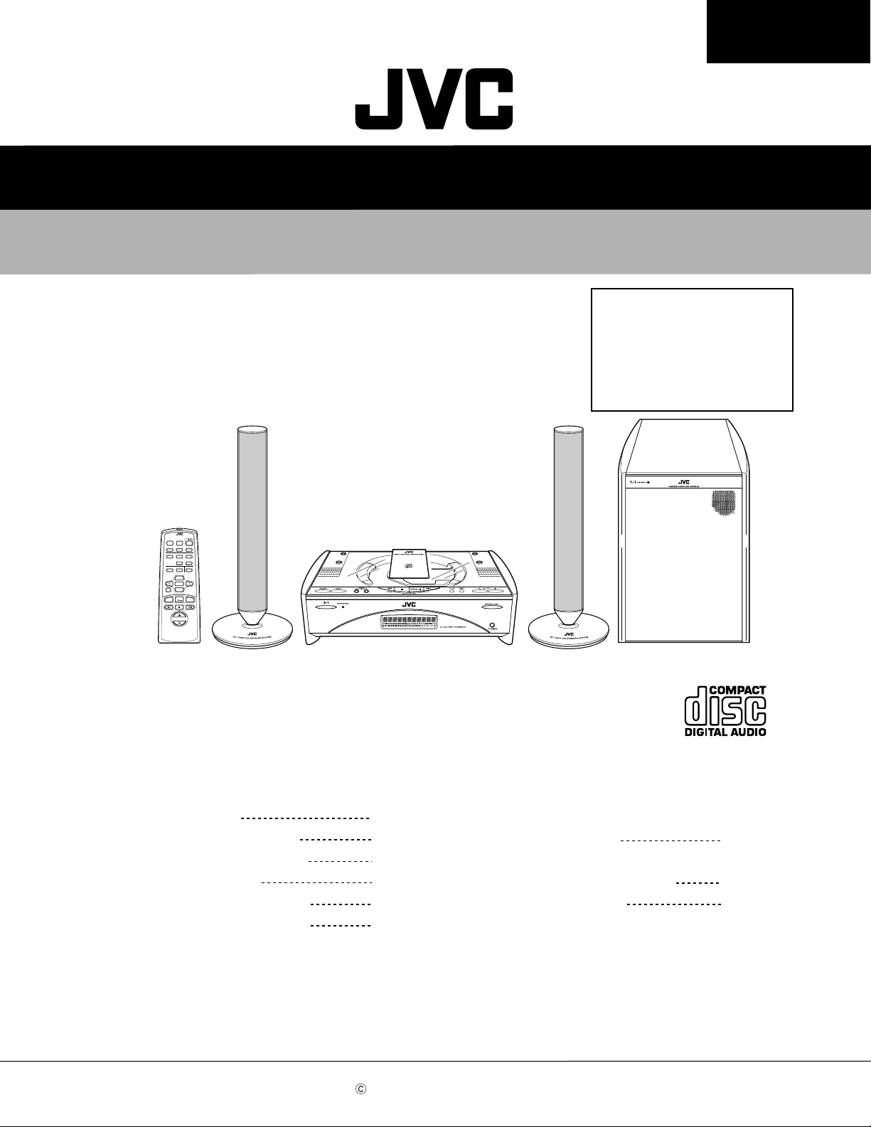
SERVICE MANUAL
COMPACT COMPONENT SYSTEM
Area suffix
UF --------------------------- China
UP --------------------------- Korea
FS-SD1000
US --------------------- Singapore
UT -------------------------- Taiwan
UW --------- Brazil,Mexico,Peru
FS-SD1000
REMOTE CONTROL RM-SFSSD1000J
STANDBY/ON
DIMMER SLEEP
AUTO
DISPLAY FM MODE
PRESET
PR
REPEATRANDOM
OGRAM
DOOR
CD
SLIDE
BASS TREBLE CANCEL
UP
SET
DOWN
FADE MUTING
CD
MD/AUX FM /AM
VOLUME
Contents
This model not have adjustment.
Safety Precautions
Preventing static electricity
Important for laser products
Disassembly method
Maintenance of laser pickup
Replacement of laser pickup
1-2
1-3
1-4
1-5
1-16
1-16
SP-PW1000SP-FSSD1000CA-FSSD1000SP-FSSD1000
Flow of functional operation
unit TOC read
Method of connecting
treatment device wire
Description of major ICs
1-17
1-18
1-19~31
COPYRIGHT 2001 VICTOR COMPANY OF JAPAN, LTD.
No.21011
Jul. 2001
Page 2
FS-SD1000
1. This design of this product contains special hardware and many circuits and components specially for safety
purposes. For continued protection, no changes should be made to the original design unless authorized in
writing by the manufacturer. Replacement parts must be identical to those used in the original circuits. Services
should be performed by qualified personnel only.
2. Alterations of the design or circuitry of the product should not be made. Any design alterations of the product
should not be made. Any design alterations or additions will void the manufacturer`s warranty and will further
relieve the manufacture of responsibility for personal injury or property damage resulting therefrom.
3. Many electrical and mechanical parts in the products have special safety-related characteristics. These
characteristics are often not evident from visual inspection nor can the protection afforded by them necessarily
be obtained by using replacement components rated for higher voltage, wattage, etc. Replacement parts which
have these special safety characteristics are identified in the Parts List of Service Manual. Electrical
components having such features are identified by shading on the schematics and by ( ) on the Parts List in
the Service Manual. The use of a substitute replacement which does not have the same safety characteristics
as the recommended replacement parts shown in the Parts List of Service Manual may create shock, fire, or
other hazards.
4. The leads in the products are routed and dressed with ties, clamps, tubings, barriers and the like to be
separated from live parts, high temperature parts, moving parts and/or sharp edges for the prevention of
electric shock and fire hazard. When service is required, the original lead routing and dress should be
observed, and it should be confirmed that they have been returned to normal, after re-assembling.
5. Leakage currnet check (Electrical shock hazard testing)
After re-assembling the product, always perform an isolation check on the exposed metal parts of the product
(antenna terminals, knobs, metal cabinet, screw heads, headphone jack, control shafts, etc.) to be sure the
product is safe to operate without danger of electrical shock.
Do not use a line isolation transformer during this check.
Plug the AC line cord directly into the AC outlet. Using a "Leakage Current Tester", measure the leakage
current from each exposed metal parts of the cabinet, particularly any exposed metal part having a return
path to the chassis, to a known good earth ground. Any leakage current must not exceed 0.5mA AC (r.m.s.).
Alternate check method
Plug the AC line cord directly into the AC outlet. Use an AC voltmeter having, 1,000 ohms per volt or more
sensitivity in the following manner. Connect a 1,500 10W resistor paralleled by a 0.15 F AC-type capacitor
between an exposed metal part and a known good earth ground.
Measure the AC voltage across the resistor with the AC
voltmeter.
Move the resistor connection to eachexposed metal part,
particularly any exposed metal part having a return path to
the chassis, and meausre the AC voltage across the resistor.
Now, reverse the plug in the AC outlet and repeat each
measurement. voltage measured Any must not exceed 0.75 V
AC (r.m.s.). This corresponds to 0.5 mA AC (r.m.s.).
0.15 F AC TYPE
1500 10W
Good earth ground
AC VOLTMETER
(Having 1000
ohms/volts,
or more sensitivity)
Place this
probe on
each exposed
metal part.
!
1. This equipment has been designed and manufactured to meet international safety standards.
2. It is the legal responsibility of the repairer to ensure that these safety standards are maintained.
3. Repairs must be made in accordance with the relevant safety standards.
4. It is essential that safety critical components are replaced by approved parts.
5. If mains voltage selector is provided, check setting for local voltage.
Burrs formed during molding may
be left over on some parts of the
chassis. Therefore, pay attention to
such burrs in the case of
preforming repair of this system.
In regard with component parts appearing on the silk-screen printed side (parts side) of the PWB diagrams, the
parts that are printed over with black such as the resistor ( ), diode ( ) and ICP ( ) or identified by the " "
mark nearby are critical for safety.
When replacing them, be sure to use the parts of the same type and rating as specified by the manufacturer.
(Except the JC version)
1-2
Page 3
FS-SD1000
Preventing static electricity
1.Grounding to prevent damage by static electricity
Electrostatic discharge (ESD), which occurs when static electricity stored in the body, fabric, etc. is discharged,
can destroy the laser diode in the traverse unit (optical pickup). Take care to prevent this when performing repairs.
2.About the earth processing for the destruction prevention by static electricity
Static electricity in the work area can destroy the optical pickup (laser diode) in devices such as CD players.
Be careful to use proper grounding in the area where repairs are being performed.
2-1 Ground the workbench
Ground the workbench by laying conductive material (such as a conductive sheet) or an iron plate over
it before placing the traverse unit (optical pickup) on it.
2-2 Ground yourself
Use an anti-static wrist strap to release any static electricity built up in your body.
(caption)
Anti-static wrist strap
Conductive material
(conductive sheet) or iron plate
3. Handling the optical pickup
1. In order to maintain quality during transport and before installation, both sides of the laser diode on the
replacement optical pickup are shorted. After replacement, return the shorted parts to their original condition.
(Refer to the text.)
2. Do not use a tester to check the condition of the laser diode in the optical pickup. The tester's internal power
source can easily destroy the laser diode.
4.Handling the traverse unit (optical pickup)
1. Do not subject the traverse unit (optical pickup) to strong shocks, as it is a sensitive, complex unit.
2. Cut off the shorted part of the flexible cable using nippers, etc. after replacing the optical pickup. For specific
details, refer to the replacement procedure in the text. Remove the anti-static pin when replacing the traverse
unit. Be careful not to take too long a time when attaching it to the connector.
3. Handle the flexible cable carefully as it may break when subjected to strong force.
4. It is not possible to adjust the semi-fixed resistor that adjusts the laser power. Do not turn it
Sub board
Attention when traverse unit is decomposed
*Please refer to "Disassembly method" in the text for pick-up and how to
detach the substrate.
1.Solder is put up before the card wire is removed from connector on
the CD substrate as shown in Figure.
(When the wire is removed without putting up solder, the CD pick-up
assembly might destroy.)
2.Please remove solder after connecting the card wire with
when you install picking up in the substrate.
Shorting
(Reverse side)
Flexible cable
1-3
Page 4
FS-SD1000
Important for laser products
1.CLASS 1 LASER PRODUCT
2.DANGER : Invisible laser radiation when open and inter
lock failed or defeated. Avoid direct exposure to beam.
3.CAUTION : There are no serviceable parts inside the
Laser Unit. Do not disassemble the Laser Unit. Replace
the complete Laser Unit if it malfunctions.
4.CAUTION : The compact disc player uses invisible laser
radiation and is equipped with safety switches which
prevent emission of radiation when the drawer is open and
the safety interlocks have failed or are
defeated. It is dangerous to defeat the safety switches.
VARNING : Osynlig laserstrålning är denna del är öppnad
och spårren är urkopplad. Betrakta ej strålen.
VARO : Avattaessa ja suojalukitus ohitettaessa olet
alttiina näkymättömälle lasersäteilylle.Älä katso
säteeseen.
5.CAUTION : If safety switches malfunction, the laser is able
to function.
6.CAUTION : Use of controls, adjustments or performance of
procedures other than those specified herein may result in
hazardous radiation exposure.
CAUTION
!
Please use enough caution not to
see the beam directly or touch it
in case of an adjustment or operation
check.
ADVARSEL : Usynlig laserstråling ved åbning , når
sikkerhedsafbrydere er ude af funktion. Undgå
udsættelse for stråling.
ADVARSEL : Usynlig laserstråling ved åpning,når
sikkerhetsbryteren er avslott. unngå utsettelse
for stråling.
REPRODUCTION AND POSITION OF LABELS
WARNING LABEL
CLASS 1
LASER PRODUCT
DANGER : Invisible laser radiation
when open and interlock or
defeated.
AVOID DIRECT EXPOSURE TO
BEAM (e)
VARO : Avattaessa ja suojalukitus
ohitettaessa olet alttiina
näkymättömälle lasersäteilylle.Älä
katso säteeseen. (d)
VARNING : Osynlig laserstrålning är
denna del är öppnad och spårren är
urkopplad. Betrakta ej strålen. (s)
ADVARSEL :Usynlig laserstråling
ved åbning , når
sikkerhedsafbrydere er ude af
funktion. Undgå udsættelse for
stråling. (f)
1-4
Page 5
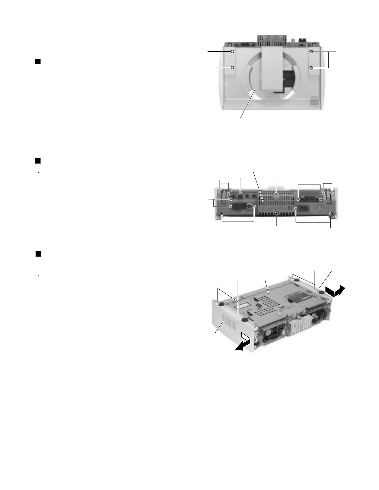
Disassembly method
FS-SD1000
<Main body>
Removing the CD door (See Fig.1)
1.
Remove the four screws A attaching the CD door on
the upper side of the body.
Removing the rear cover (See Fig.2)
Piror to performing the following procedure, remove
the CD door.
1.
Remove the ten screws B and the five screws C
attaching the rear cover on the back of the body.
A
B
C
CD door
Rear cover
B
Fig.1
C
B
A
C
Removing the right and left covers
(See Fig.3)
Prior to performing the following procedure, remove
the CD door, the rear cover.
1.
Remove the four screws D attaching the side covers
on the bottom of the body.
2.
Move the left cover backward and remove outward.
Also remove the right cover in the same way.
Left cover
D
B
Bottom
B
Fig.2
Fig.3
Right cover
D
B
1-5
Page 6
FS-SD1000
Removing the front panel assembly
(See Fig.4 to 6)
Prior to performing the following procedure, remove
the CD door, the rear cover and the side covers.
1.
Remove the three screws E on the bottom of the
body.
2.
Release two joints a and two joints b on both sides
of the body using a screwdriver and remove the front
panel assembly toward the front.
Front panel assembly
(Left side)
E
Bottom
Front panel assembly
Fig.4
Front panel assembly
(Right side)
Joints a
Removing the CD mechanism base
assembly (See Fig.7 to 14)
Prior to performing the following procedure, remove
the CD door, the rear cover, the side covers and the
front panel assembly.
1.
Disconnect the card wire from connector CN104 and
CN105 of the main board in the front part of the
body. Disconnect the card wire from CN101 of the
main board on the right side, and the wire from
CN705 and CN708 of the CD mechanism base
assembly respectively.
2.
Remove the four screws F attaching the CD
mechanism base assembly on the upper side of the
body. Remove the screw I attaching the earth
terminal on the right side.
Joints b
F
CD mechanism base assembly
Fig.6Fig.5
F
Fig.7
CD mechanism base assembly
1-6
CN104
CN105
Fig.8
Main bard
Page 7
FS-SD1000
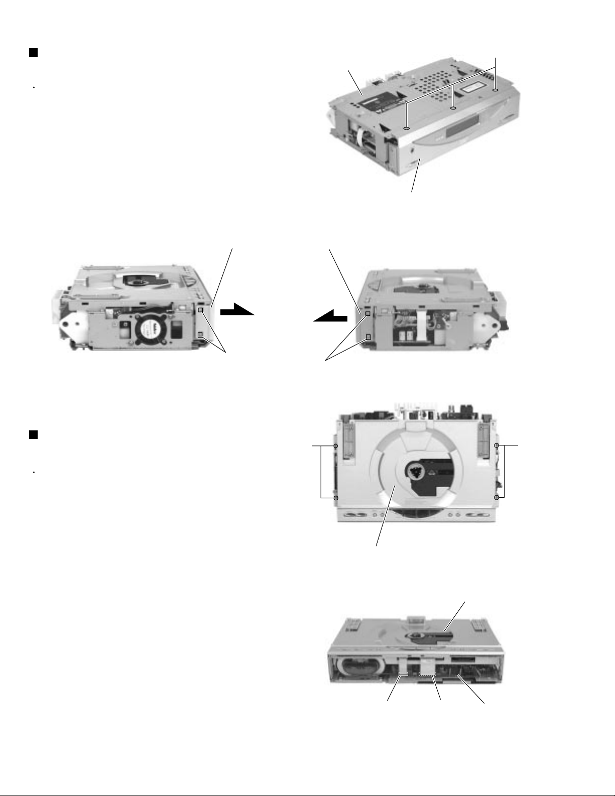
3.
Remove the screw G attaching the power amplifier
board on the back of the body. Disconnect the wire
from connector CN301 and pull the power amplifier
board fully outward.
4.
Raise the right and left door arms by turning the gear
a in the rear of the power amplifier board.
5.
After the CD mechanism base assembly is detached
from the door arms, pull the CD mechanism base
assembly toward the front and disconnect the wire
from connector CN804 on the left side of the door
arm board.
6.
Pull out the CD mechanism base assembly toward
the front.
CD mechanism base assembly
Main board
CN101
F
F
I
CN705
CN708
Fig.9
CD mechanism base assembly
CD mechanism base assembly
I
Door arm
CD mechanism base assembly
Gear a
Fig.12
Door arm
Power amplifier board
CN804
CD mechanism base assembly
Power amplifier board
G
Fig.10
CN301
Fig.11
Door arm board (L)
CN804
Fig.14
Gear a
Fig.13
1-7
Page 8
FS-SD1000
Removing the door arm assembly / the
door arm board (R) and (L)
(See Fig.15 to 20)
Prior to performing the following procedure, remove
the rear cover, the side covers, the front panel
assembly and the CD mechanism base assembly.
1.
In case that the upper parts of the door arms
attached to the CD door are not level, let down them
to the level position by turning the gear a in the
direction of the arrow.
ATTENTION:
2.
Remove the four screws H on the upper side and
the one screw I on the left side of the body.
3.
Remove the four screws J attaching the door arm
board (L) and (R) on both sides of the door arm
assembly.
When the door arms incline, the door
arm assembly and the door arm board
(R) and (L) may not be removed.
Door arm
Door arm
Door arm board (L)
Fan motor
Fig.15
Door arms (Attached to the CD door)
Door arm board (R)
Door arm assembly
H
Fig.17
J
Door arm assembly
Fig.16
Door arm assembly
Fig.18
J
Door arm board (R)
H
Door arm board (L)
1-8
I
J
Fig.19
J
Fig.20
Page 9
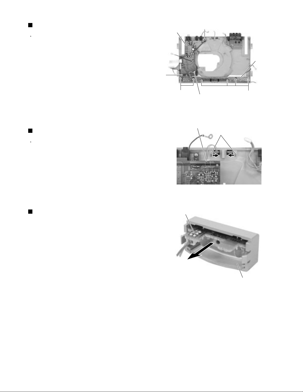
FS-SD1000
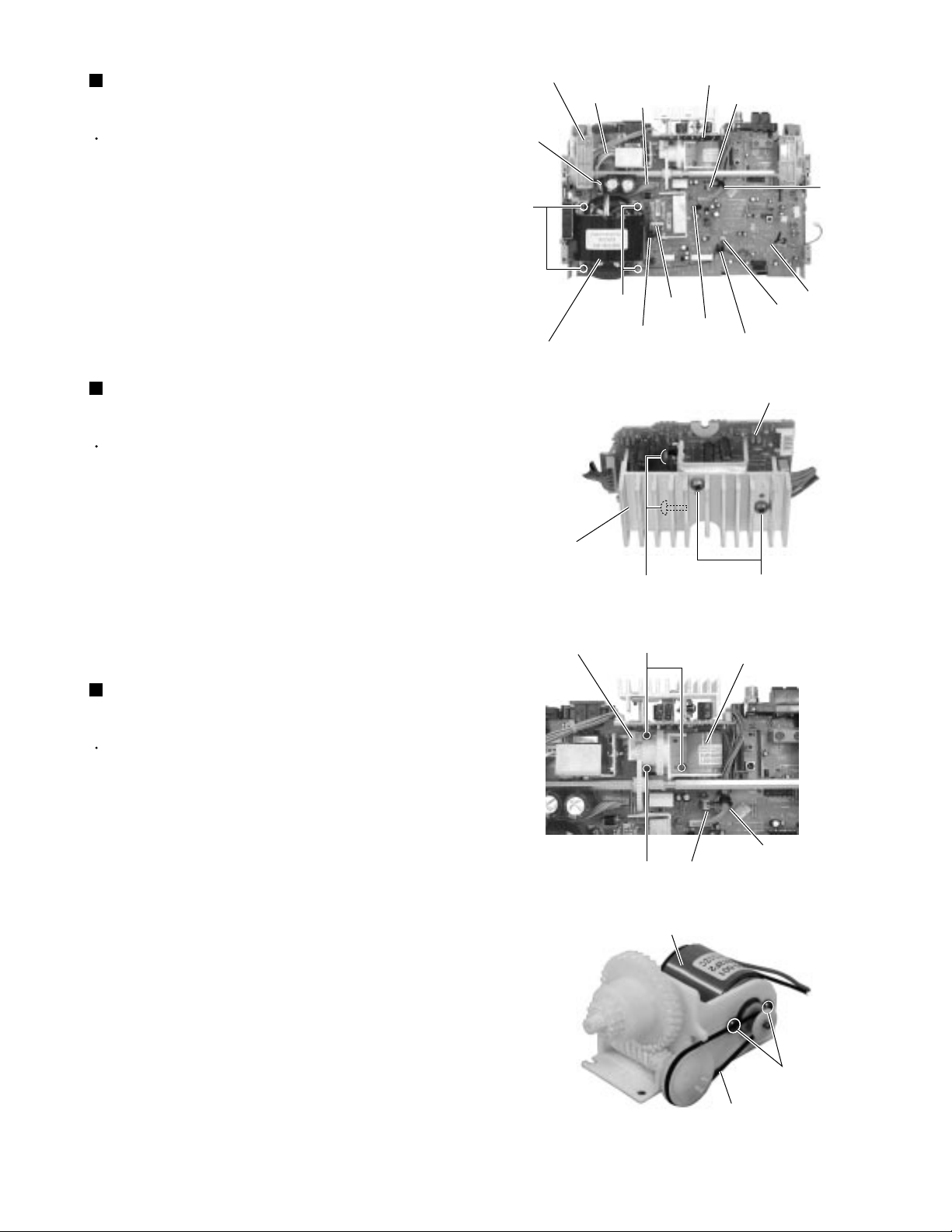
Removing the power amplifier board
(See Fig.21 and 22)
Prior to performing the following procedure, remove
the CD mechanism base assembly.
1.
Disconnect the wires from connector CN102 and
CN193 on the main board and release them from the
cord stopper respectively.
2.
Remove the two screws K and the two screws L
attaching the heat sink and the power amplifier
board.
Removing the transformer assembly
(See Fig.21)
Prior to performing the following procedure, remove
the CD mechanism base assembly.
1.
Disconnect the wires from connector CN191 and
CN192 on the main board and release them from the
cord stopper respectively.
Door arm assembly
CN191
Cord stopper
M
Cord stopper
Transformer assembly
Heat sink
Power amplifier board
CN193
CN192
M
CN102
Fig.21
CN106
Cord
stopper
Main board
CN181
Cord stopper
Power amplifier board
2.
Remove the four screws M attaching the transformer
assembly.
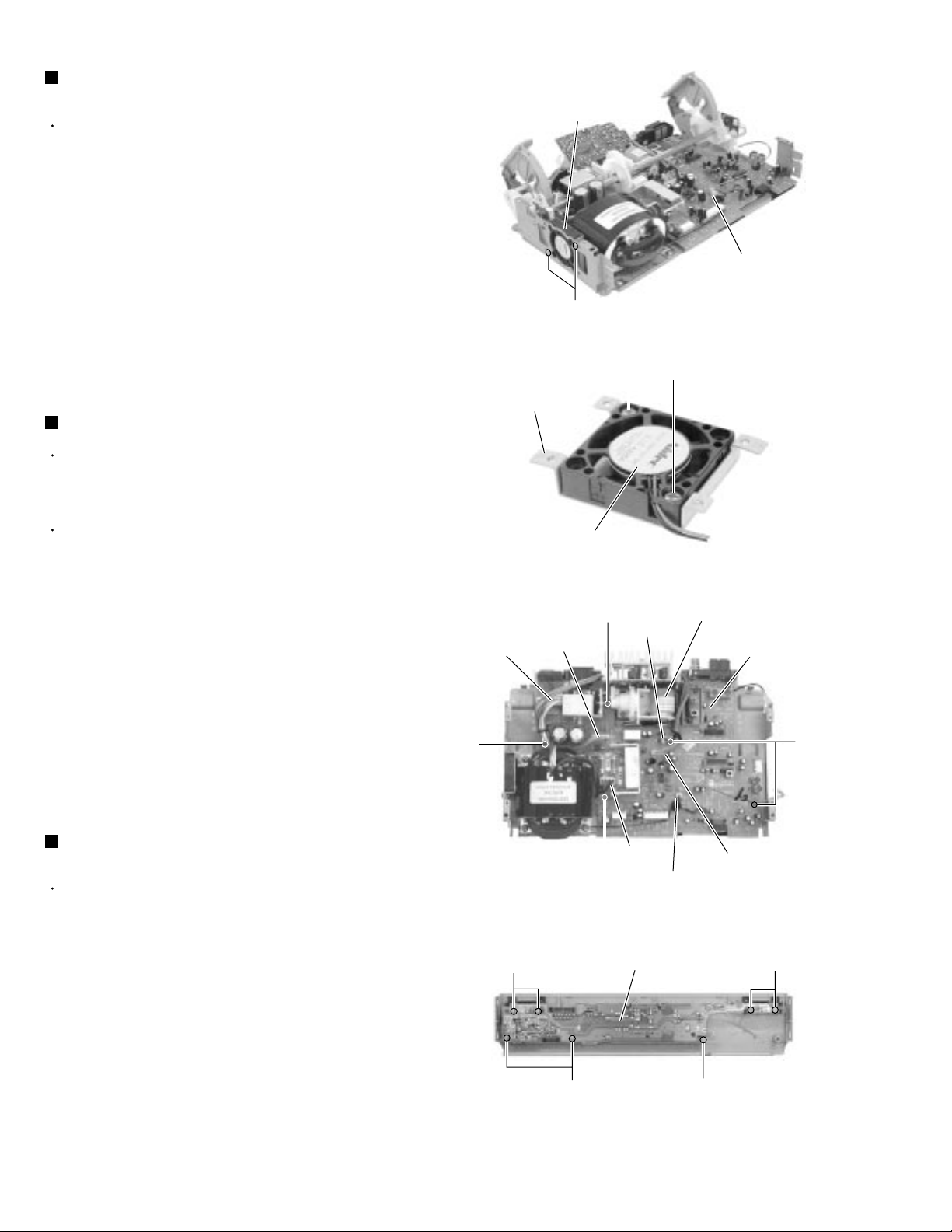
Removing the gear motor assembly
(See Fig.23 and 24)
Prior to performing the following procedure, remove
the CD mechanism base assembly and the door arm
assembly.
1.
Disconnect the wires from connector CN106 on the
main board and release it from the cord stopper.
2.
Remove the three screws N attaching the gear
motor assembly. Remove the gear motor assembly
with the gear motor stopper.
3.
Remove the belt from the gear motor assembly.
4.
Remove the two screws O from the gear motor
assembly.
Gear motor stopper
L
N
N
Motor
K
Fig.22
Gear motor assembly
Cord stopper
CN106
Fig.23
Fig.24
O
Belt
1-9
Page 10
FS-SD1000
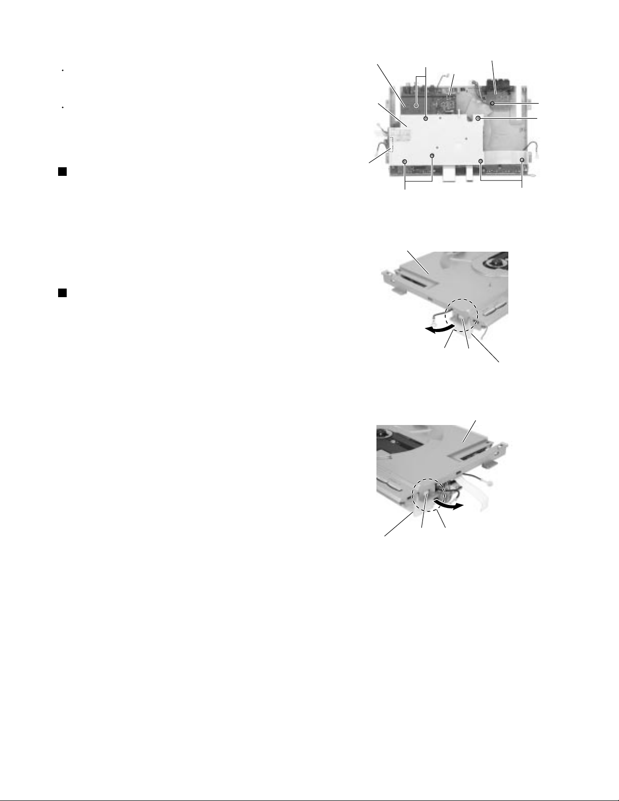
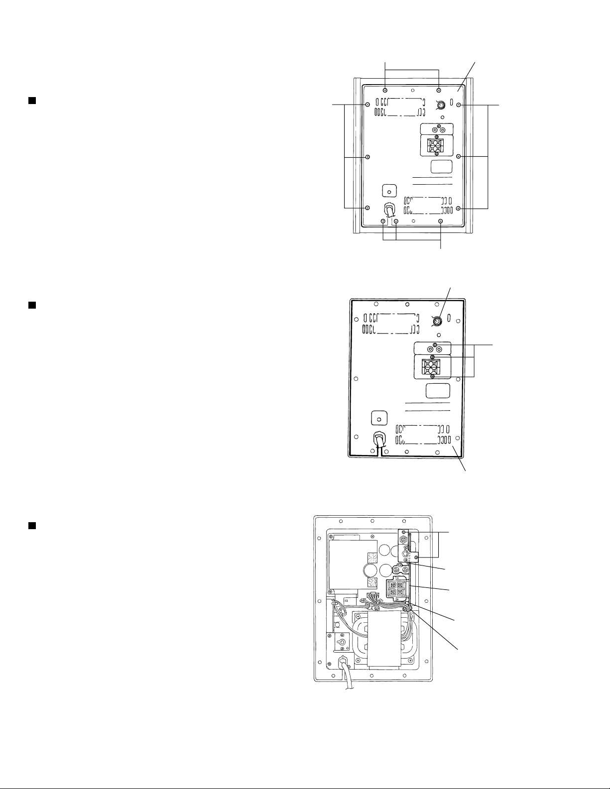
Removing the fan motor assembly
(See Fig.25 and 26)
Prior to performing the following procedure, remove
the CD mechanism base assembly.
1.
Disconnect the wires from connector CN181 on the
main board.
2.
Remove the two screws P on the left side of the
body. Move the fan motor assembly upward to
remove it from the base chassis.
3.
Remove the two screws Q and the fan motor from
the fan bracket.
Removing the main board (See Fig.27)
Prior to performing the following procedure, remove
the CD mechanism base assembly and the door arm
assembly.
Fan bracket
Fan motor
P
Fig.25
Q
Main board
CN181
To facilitate operation process, remove the gear
motor assembly before performing the following
procedure.
1.
Disconnect the wires from connector CN102, CN106,
CN191, CN192, CN193 and CN181 on the main
board.
2.
Remove the five screws R attaching the main board
with the cord stopper.
<Front panel assembly>
Removing the front panel board
(See Fig.28)
Prior to performing the following procedure, remove
the front panel assembly.
1.
Remove the seven screws S attaching the front
panel board inside the front panel assembly.
CN191
R
S
Fan motor
CN193
Front panel board
R
R
Fig.26
Gear motor assembly
CN106
CN192
CN181
Fig.27
Main board
R
CN102
S
1-10
S
S
Fig.28
Page 11
FS-SD1000
<CD mechanism base assembly>
Prior to performing the following procedure, remove
the CD mechanism base assembly.
Refer to "Dismantling and assembling the CD
mechanism assembly" on page 1-5 for the treatment
of optical pickup.
Removing the speaker terminal board
(See Fig.29)
1.
Remove the screw T attaching the speaker terminal
board on the underside of the CD mechanism base
assembly.
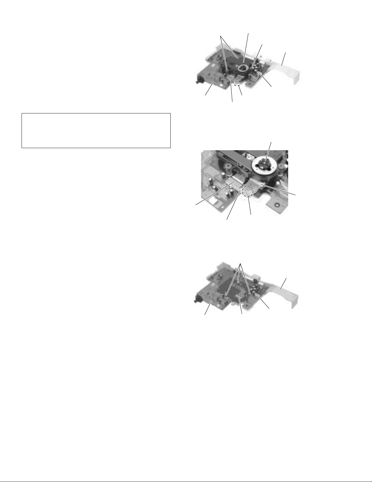
Removing the CD mechanism board / CD
mechanism assembly (See Fig.29 to 34)
1.
Turn over the CD mechanism base assembly and
disconnect the wires from connector CN703 and
CN706 on the CD mechanism board.
2.
Remove the seven screws U attaching the CD
mechanism cover and the CD mechanism board.
CD mechanism board
CD mechanism
cover
CN703
U
CD mechanism assembly
U
Joint c
Speaker terminal board
CN706
T
U
U
Fig.29
Tab
CD mechanism cover
Fig.30
3.
Turn back the CD mechanism assembly and detach
the CD mechanism cover while pulling the CD
mechanism assembly outward to release the two
joint tabs marked c.
CD mechanism cover
Tab
CD mechanism assembly
Joint c
Fig.31
1-11
Page 12
FS-SD1000
4.
Solder the short circuit land on the sub board.
5.
Disconnect the wire from connector CN605 on the
main board.
Disconnect the sub board from connector CN603 on
the main board while peeling off the adhesive tape
on the underside of the sub board.
6.
Remove the CD mechanism assembly from the three
shafts of the CD mechanism
cover.
Cushion
CD mechanism board
Sub board
CD mechanism assembly
Cushion
CD mechanism cover
CN605
Short circuit land
ATTENTION:
When reassembling, confirm that the
cushion of the CD mechanism
assembly is reattached to the three
shafts.
7.
Remove the CD mechanism board from the CD
mechanism cover.
CN606
Sub board
Fig.32
CD mechanism assembly
Main board
CN603
Short circuit land
Fig.33
Shafts
CD mechanism cover
1-12
CD mechanism board
CN603
CN605
Fig.34
Page 13
FS-SD1000
Removing the jack board (See Fig.35)
Prior to performing following procedure, remove the
CD mechanism board.
1.
Disconnect the wire from connector CN502 on the
jack board.
2.
Remove the two screws V attaching the jack board.
Removing the switch board (See Fig.35)
Prior to performing following procedure, remove the
CD mechanism board.
1.
Disconnect the wire from connector CN502 on the
jack board.
Jack board
V
W
CD mechanism board
CN502
CN706
V
Switch board
W
Fig.35
Tabs d
2.
Remove the six screws W attaching the switch
board.
Removing the LED board
(See Fig.36 and 37)
1.
Disconnect the harness from connector CN706 on
the CD mechanism board on the underside of the
CD mechanism base assembly.
2.
Push inward the two tabs d attaching the LED board
case and release them.
3.
Pull out the LED board from the LED board case.
Fig.36
LED board
LED board case
Fig.37
1-13
Page 14
FS-SD1000
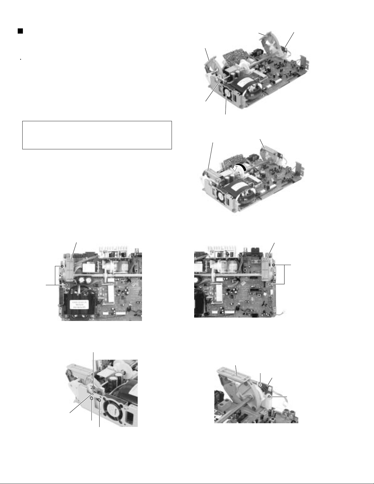
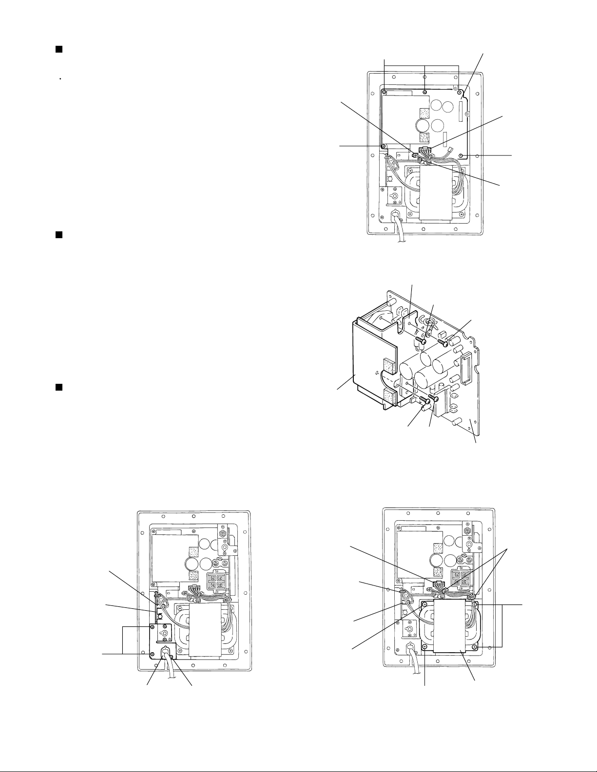
Power woofer section
<Main body>
Removing the amplifier assembly
(See Fig.1)
1.
Remove the eleven screws A attaching the amplifier
assembly on the back of the body.
2.
Disconnect each relay harness connected to the
speaker and the LED indicator board.
<Amplifier>
Removing the cover (See Fig.2)
1.
Pull out the volume knob from the amplifier.
A
A
Fig.1
Amplifier board
A
A
Volume knob
2.
Remove the three screws B on the amplifier.
Removing the Input amplifier / filter
board assembly (See Fig.3)
1.
Cut off the band under the input amplifier / filter
board assembly.
2.
Disconnect the harness from connector CN251.
3.
Remove the two screws C attaching the input
amplifier / filter board assembly. Pull and disconnect
connector CN211 from the body.
B
Cover
Fig.2
C
CN211
Input amplifier / filter
board assembly
CN251
Band
1-14
Fig.3
Page 15
FS-SD1000
Removing the amplifier board assembly
(See Fig.4 and 5)
Prior to performing procedure, remove the input
amplifier / filter board assembly.
1.
Disconnect the harness from connector CN291 and
CN281 on the amplifier board assembly.
2.
Remove the six screws D attaching the amplifier
board assembly.
3.
Remove the two screws E attaching the heat sink 1
and the two screws F attaching the heat sink 2
respectively.
Removing the transformer assembly
(See Fig.6)
1.
Cut off the three bands fastening the harnesses
extending from the transformer assembly.
2.
Disconnect the harness from connector CN291 on
the amplifier board assembly and from CN299 on the
power board assembly.
CN281
D
D
Heat sink 2
Amplifier board assembly
CN291
D
D
Fig.4
E
F
3.
Remove the four screws G attaching the transformer
assembly.
Removing the power board assembly
(See Fig.7)
1.
Disconnect the harness from connector CN299 on
the power board assembly and cut off the band.
2.
Remove the three screws H assembly.
3.
Remove the cord stopper.
CN299
Power board
assembly
Heat sink 1
Amplifier board
assembly
CN291
Band
Power board
assembly
CN299
E
F
Amplifier board assembly
Fig.5
Bands
G
H
Cord stopper
Fig.7
H
G
Transformer assembly
G
Fig.6
1-15
Page 16
FS-SD1000
Maintenance of laser pickup
(1) Cleaning the pick up lens
Before you replace the pick up, please try to
clean the lens with a alcohol soaked cotton
swab.
(2) Life of the laser diode
When the life of the laser diode has expired,
the following symptoms will appear.
1. The level of RF output (EFM output:amplitude
of eye pattern) will below.
Is the level of
RFOUT under
1.25V 0.22Vp-p?
YES
O.K
NO
Replace it.
Replacement of laser pickup
Turn off the power switch and,disconnect the
power cord from the ac outlet.
Replace the pickup with a normal one.(Refer
to "Pickup Removal" on the previous page)
Plug the power cord in,and turn the power on.
At this time,check that the laser emits for
about 3seconds and the objective lens moves
up and down.
Note: Do not observe the laser beam directly.
Play a disc.
Check the eye-pattern at TP1.
Finish.
(3) Semi-fixed resistor on the APC PC board The semi-fixed resistor on the APC printed circuit board which is
attached to the pickup is used to adjust the laser power.Since this adjustment should be performed to match the
characteristics of the whole optical block, do not touch the semi-fixed resistor.
If the laser power is lower than the specified value,the laser diode is almost worn out, and the laser pickup should
be replaced.
If the semi-fixed resistor is adjusted while the pickup is functioning normally,the laser pickup may be damaged
due to excessive current.
1-16
Page 17
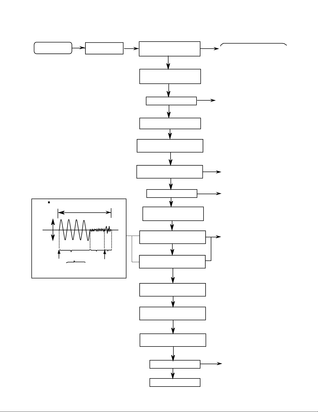
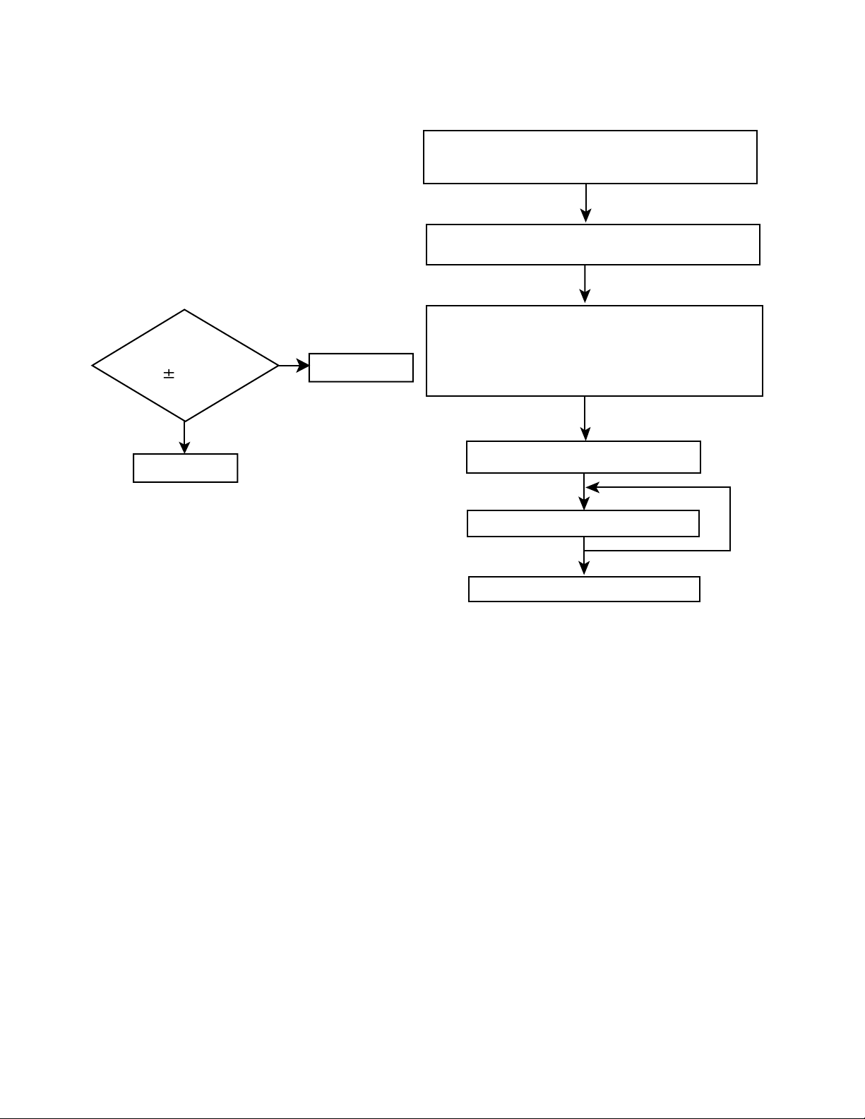
Flow of functional operation until TOC read
Power ON
Play Key
Slider turns REST
SW ON.
Automatic tuning
of TE offset
Confirm that the voltage at the pin4
of CN605 is "H"/"L"/"H".
FS-SD1000
Check Point
Tracking error waveform at TOC reading
Approx.3sec
Tracking
servo
off states
Automatic measurement
of TE amplitude and
automatic tuning of
TE balance
VREF
pin 25 of
IC601(TE)
Approx
1.8V
Disc states
to rotate
Tracking
servo
on states
Disc to be
braked to stop
TOC reading
finishes
500mv/div
2ms/div
Fig.1
Laser ON
Detection of disc
Automatic tuning of
Focus offset
Automatic measurement of
Focus S-curve amplitude
Disc is rotated
Focus servo ON
(Tracking servo ON)
Automatic measurement of
Tracking error amplitude
Automatic tuning of
Tracking error balance
Check that the voltage at the
pin40 of IC603 is + 5V?
Confirm that the Focus error
S-cuve signal at the pin28 of
IC603 is approx.2Vp-p
Confirm that the signal from
pin24 IC603 is 0V as a
accelerated pulse during
approx.400ms.
Confirm the waveform of
the Tracking error signal.
at the pin 25 of IC601 (R6009)
(See fig-1)
Automatic tuning of
Focus error balance
Automatic tuning of
Focus error gain
Automatic tuning of
Tracking error gain
TOC reading
Play a disc
Confirm the eys-pattern
at the lead of TP602
1-17
Page 18
FS-SD1000
Method of connecting treatment device wire
First short-circuit the pickup circuit before removing the pickup. Then carry out the replacement.
Refer to "Disassembling and assembling the traverse unit".
KSM-900AAH
Sub board
(Reverse side)
Shorting
Flexible cable
When the KSM-900AAH mechanism is used, the expansion cable is used as follows.
EXTFSSD5-JIG
extension wire
QUQB12-0840CJ
8pin card wire
QUQB12-0940DJ
9pin card wire
QUQB12-1840DJ
18pin card wire
1-18
QUQB12-1640DJ
16pin card wire
EXTKSM900-JIG
Sub board
Page 19
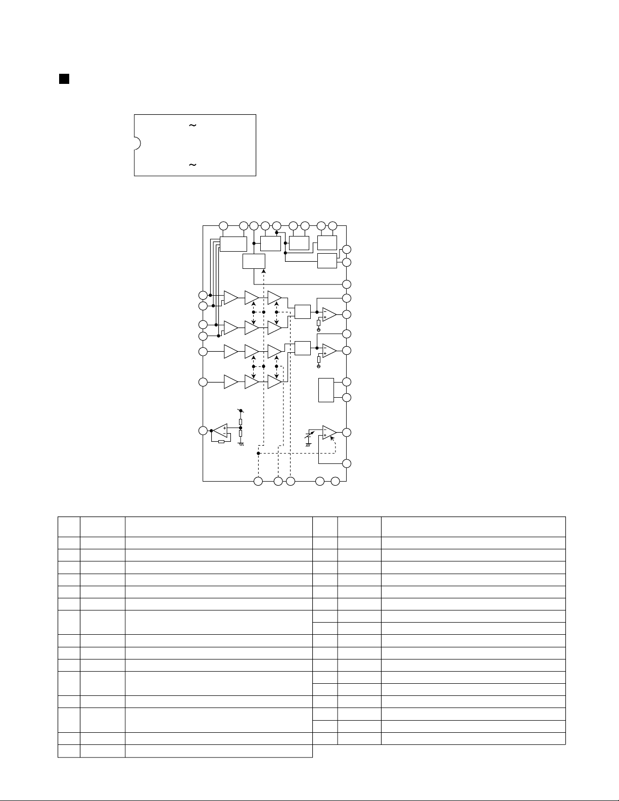
Description of major ICs
AN22000A (IC601) : RF & Servo amp
1. Pin layout
32 17
116
FS-SD1000
2. Block
3. Function
VREF
ARF
RF IN
C.AGC
RF OUT
RFN
RF_EQ AGC BDO
32
A
C
B
D
E
F
AMP
31
30
AMP
29
27
AMP
AMP
28
17
7654
NRFDET
BCA
GCA
BCA
GCA
BCA
GCA
BCA
GCA
24
GCTL TBAL FBAL
BDO
CBDO
8
SUBT
SUBT
26 25 16 3
OFTR
COFTR
14131211
OFTR
3TENV
VDET
CDDG VCC
9
10
15
22
23
21
20
19
18
2
1
CEA
3TOUT
NRFDET
FEN
FEOUT
TEN
TEOUT
TEBPF
VDET
LD
PD
Pin
Symbol Function
No.
1
2
3
4
5
6
7
PD
LD
VCC
RFN
RF OUT
RF IN
C.AGC
APC Amp. Input terminal
APC Amp.Output terminal
Power supply terminal
RF addition Amp.Reversing input terminal
RF addition Amp.Output terminal
AGC input terminal
Terminal of connection of capacity of AGC loop
filter.
8
10
11
ARF
9
CEA
3TOUT
CBDO
AGC output terminal
Capacity connection terminal for HPF-Amp.
3TENV output terminal
Capacity connection terminal for RF shade side
envelope detection
12
13
BDO
COFTR
BDO output terminal
Capacity connection terminal for RF discernment
side envelope detection
14
15
OFTR
NRFDET
OFTR output terminal
NRFDET output terminal
Pin
Symbol Function
No.
16
17
18
19
20
21
22
23
24
25
26
27
28
29
30
31
32
CDDG
VREF
VDET
TEBPF
TEOUT
TEN
FEN
FEOUT
GCTL
FBAL
TBAL
E
F
D
B
C
A
Earth terminal
VREF output terminal
VDET output terminal
VDET input terminal
TE Amp. output terminal
TE Amp. reversing input terminal
FE Amp. reversing input terminal
FE Amp. output terminal
Terminal GCTL & APC
FBAL control terminal
TBAL control terminal
Tracking signal input terminal 1
Tracking signal input terminal 2
Focus signal input terminal 4
Focus signal input terminal 2
Focus signal input terminal 3
Focus signal input terminal 1
1-19
Page 20

FS-SD1000
UPD780024AGKB19 (IC701) : CPU
1. Pin layout
64 ~ 49
1
48
2. Block diagram
~
16
17 ~ 32
16-bit TIMER/
EVENT COUNTER
8-bit TIMER/
EVENT COUNTER50
8-bit TIMER/
EVENT COUNTER51
WATCHDOG TIMER
WATCH TIMER
SERIAL
INTERFACE30
33
~
PORT0
PORT1
PORT2
PORT3
78K/0
CPU
CORE
ROM
(32K
BYTE)
PORT4
PORT5
SERIAL
INTERFACE31
UART0
A/D CONVERTER
INTERRUPT
CONTROL
BUZZER OUTPUT
CLOCK OUTPUT
CONTROL
RAM
(1024
BYTE)
VDD0 VDD1 Vss0 Vss1 IC
PORT6
PORT7
EXTERNAL
ACCESS
SYSTEM
CONTROL
1-20
Page 21

FS-SD1000
3. Pin function
Pin
No.
10
11
12
13
14
15
16
17
18
19
20
21
22
23
24
25
26
27
28
29
30
31
32
33
34
35
36
37
38
39
40
41
42
43
44
45
46
47
48
49
50
51
52
53
54
55
56
57
58
59
60
61
62
63
64
1
2
3
4
5
6
7
8
9
Symbol I/O Function
MT0
MT1
MTS
BLCTL
AHB
SMUTE
TUST
CDLED
VSS0
VDD0
MPX
RDSDI
DRMUTE
SCD
TUDATA(I)
TUDATA(O)
TUCK
SUBQ
XRST
SQCK
MLD
M DATA
MCLK
VDD1
AVSS
S TAT
REST
KEY1
KEY2
KEY3
SAFETY
LDCK
VERSION
AVREF
AVDD
RESET
XT2
XT1
IC
X2
X1
VSS1
REM
RDSCK
XKILL
BEAT
BUP
+BCTL
V DATA
VCLK
DOOR1
DOOR2
DOOR3
LOMUTE
RS
E
D84
D85
D86
D87
DIMMER
POUT
FTU
FCD
O
CD door motor control signal 0 output
O
CD door motor control signal 1 output
O
Motor speed control output (L:Normal, H:Slow)
O
Back light power supply control output
O
AHB ON/OFF control signal output (L:ON, H:OFF)
O
System mute control signal output
O
Tuner control strove output
O
CD LED control signal output (L:OFF, H:ON)
-
Ground at port section
-
Power supply at port section
I
Stereo indicator control signal input (L:Stereo)
I
RDS data input
O
Driver mute output
I
Voltage detection for safety of CD
I
Tuner control data input
O
Tuner control data output
O
Tuner control clock output
I
CD control Q code input
O
CD control reset signal output
O
CD control Q code clock signal output
O
CD control command load signal output
O
CD control command data signal output
O
CD control command clock signal output
-
Power supply without port section
-
Ground of A/D converter
I
CD control status signal input
I
CD rest switch detection signal input
I
Main body top section tact switch detection signal input
I
Main body top section tact switch detection signal input
I
Main body front section tact switch detection signal input
I
Voltage detection for safety
I
CD door motor lock detection signal input
I
Version detection
I
Reference voltage input for A/D converter
-
Analog power supply for A/D converter
I
System reset signal input
-
Sub clock
I
Sub clock signal input 32.768kHz
I
Connect to VSS0 or VSS1
-
Main clock
I
Main clock signal input 4.19MHz
-
Ground without port section
I
Remote controller signal input
I
RDS clock signal input
O
Sub clock OSC control signal output
O
Main clock shift control signal output
I
Back up detection signal input
O
Power supply control at back up operating
O
BD3861FS (VOL & FUNC IC) control data signal output
O
BD3861FS (VOL & FUNC IC) control clock signal output
I
Cd door position detection switch input
I
CD door position detection switch input
I
CD door position detection switch input
O
LINE OUT muting control signal output
O
LCD driver control resistor select signal output
O
LCD driver control enable signal output
O
LCD driver control data bus signal output
O
LCD driver control data bus signal output
O
LCD driver control data bus signal output
O
LCD driver control data bus signal output
O
Back light DIMMER control signal output
O
Power supply control signal output for amp section
O
Power supply control signal output for TUNER function
O
Power supply control signal output for CD function
UPD780024AGKB19
1-21
Page 22

FS-SD1000
BA15218F-XE (IC102) : Dual operation amplifier
1. Pin layout
OUT1 1
-IN1 2
+IN1 3
VEE 4
2. Block diagram
Vcc
-IN
+IN
1
2
R1
Q5
Q1
Q2
D1
Q3 Q4
8 Vcc
7 OUT2
6 -IN2
5 +IN2
C2
R5
Q6
Q9
Q8
Q10
Q7
R7
Q11
R6
Q12
R8
Q18Q13
OTHER
CH
Q19
Q17Q16
C1
R3R2
R4
VEE
GP1U271X (IC801) : Receiver for remote controller
+
–
Amp.
Limiter
B.P.F
Demodulator
OUTPUT
Integrator
GND
Q14 Q15Q114
Comparator
VCC
R9
Vout
1-22
Page 23

BD3861FS-X (IC501) : Audio sound control
1. Pin layout
32 18
117
2. Block diagram
32 31 30 29 28 27 26 25 24 23 22 21 20 19 18 17
FS-SD1000
0dB~
-70dB
Vcc/2 Vcc/2
Vcc/2
Vcc/2
25k
25k
12345678910111213141516
25k
25k
25k
25k
25k
25k
Treble1
f0=10kHz
25k
25k
Treble2
f0=10kHz
Vcc/2
Vcc/2
25k
25k
Middle2
f0=1kHz
25k
25k
25k
25k
Middle1
f0=1kHz
25k
25k
25k
25k
Bass1
f0=90Hz
12k
100k
0dB~
-59dB
24k
Vcc/2
Vcc/2
Bass2
f0=90Hz
0dB~
-59dB
Vcc/2
Vcc/2
Logic
3. Pin function
Pin
Symbol SymbolFunction Function
No.
1
2
3
4
5
6
7
8
9
10
11
12
13
14
15
16
A1
A2
B1
B2
C1
C2
D1
D2
E1
E2
MIC
FIL
GND
DATA
CLK
Vcc
CH1 input pin A
CH2 input pin A
CH1 input pin B
CH2 input pin B
CH1 input pin C
CH2 input pin C
CH1 input pin D
CH2 input pin D
CH1 input pin E
CH2 input pin E
Microphone input pin
Filter pin
Ground pin
Serial data latch receiving pin
Serial clock receiving pin
Power supply pin
17
18
BASS21
19
BASS22
20
21
BASS11
22
BASS12
23
24
25
26
27
28
29
30
31
32
OUT2
OUT1
MID11
MID12
MID21
MID22
TRE2
TRE1
VOL1
VOL2
GOUT2
GOUT1
CH2 output pin
CH2 bass filter setting pin
CH2 bass filter setting pin
CH1 output pin
CH1 bass filter setting pin
CH1 bass filter settingpin
CH1 middle filter setting pin
CH1 middle filter setting pin
CH2 middle filter setting pin
CH2 middle filter setting pin
CH2 treble filter setting pin
CH1 treble filter setting pin
CH1 input volume input pin
CH2 input volume input pin
CH2 input gain output pin
CH1 input gain output pin
1-23
Page 24

FS-SD1000
KIA78S06P-T (IC702) : Regulator
1. Pin layout 2. Block diagram
3 INPUT
1 2 3
Z1
Q14
Q1
R9
Q16
Q2 Q7
R11 R10
R1
Q4
Q3
Q6
C1
R2
Q8
R3
NJM4580D-D (IC101,IC211,IC213) : Dual ope amp.
1. Pin layout & Block diagram
A OUT 1
8 V+
R4
Q9
Q5
Q10
Q11
Q12
R8
Q13
R7R5R6
1 OUTPUT
2 COMMON
A -IN 2
7 B OUT
AB
A +IN 3
V- 4
6 B -IN
5 B +IN
TC74HCU04AP (IC251) : 2ch NOR gate
1. Pin layout & Block diagram 2.True table
1A
1Y
2A
2Y
3A
3Y
GND
1
2
3
4
5
6
7
14
13
12
11
10
9
8
VCC
6A
6Y
5A
5Y
4A
4Y
A
L
H
Y
H
L
1-24
Page 25

LA4905 (IC301) : 2ch BTL power IC
1. Pinlayput
123
FS-SD1000
2. Block diagram
STBY
D.C
PRE GND
IN 1
21
20
2
3
Standby SW
Ripple
filter
Input amplifier
Vcc Vcc(SW)
10
Switching
regulator block
H.L.S.
ABCD
H.L.S. :
Higher
Level signal
selector
Nonlinear/output stage
CH 1
11
Amplifier output stage
SW
drive
8
9
SW B
15
SW E
14
SW OUT1
12
SW OUT2
13
SW GND
16
A
+OUT 1
7
PWR GND 1
5
B
BEEP
IN 2
ON TIME
4
1
23
BEEP
amplifier
Input amplifier
ON MUTE
muting circuit
Power supply/ground shorting
protection circuit
Overvoltage/thermal protection
circuit
CH 2
Nonlinear amplifier/output stage
Pop noise
prevention circuit
-OUT 1
6
C
D
18
19
17
22
-OUT 2
PWR GND 2
+OUT 2
N.C.
1-25
Page 26

FS-SD1000
LA6541-X (IC601) : Servo driver
1. Pin layout & Block diagram
Vcc Vref Vin4 Vg4 Vo8 Vo7
24 23
11k
ohm
22
21
20
19
Vcc
Gnd
Vo6 Vo5 Vg3 Vin3 Cd Res
18
17 16
- +
- +
Level
shift
Level
shift
11k
ohm
1
2
3456
Vcc Mute Vin1 Vg1 Vo1 Vo2 Vo3 Vo4 Vg2 Vin2 Reg
B T L
driver
B T L
driver
Gnd
B T L
driver
B T L
driver
7 8 9101112
Level
shift
Level
shift
2. Pin function
Pin
Symbol Function
No.
1
10
11
12
13
14
15
16
17
18
19
20
21
22
23
24
2
3
4
5
6
7
8
9
Vcc
Mute
Vin1
Vg1
Vo1
Vo2
Vo3
Vo4
Vg2
Vin2
Reg Out
Reg In
Res
Cd
Vin3
Vg3
Vo5
Vo6
Vo7
Vo8
Vg4
Vin4
Vref
Vcc
Power supply (Shorted to pin 24)
All BTL amplifier outputs ON/OFF
BTL AMP 1 input pin
BTL AMP 1 input pin (For gain adjustment)
BTL AMP 1 input pin (Non inverting side)
BTL AMP 1 input pin (Inverting side)
BTL AMP 2 input pin (Inverting side)
BTL AMP 2 input pin (Non inverting side)
BTL AMP 2 input pin (For gain adjustment)
BTL AMP 2 input pin
External transistor collector (PNP) connection. 5V power supply output
External transistor (PNP) base connection
Reset output
Reset output delay time setting (Capacitor connected externally)
BTL AMP 3 input pin
BTL AMP 3 input pin (For gain adjustment)
BTL AMP 3 output pin (Non inverting side)
BTL AMP 3 output pin (Inverting side)
BTL AMP 4 output pin (Inverting side)
BTL AMP 4 output pin (Non inverting side)
BTL AMP 4 output pin (For gain adjustment)
BTL AMP 4 output pin
Level shift circuit's reference voltage application
Power supply (Shorted to pin 1)
15
11k
ohm
14
13
RESET
Regulator
11k
ohm
out
Reg
In
1-26
Page 27

LC72136N (IC2) : PLL frequency synthesizer
1. Pin layout
FM/AM
CLOCK
FM/ST/VCO
AM/FM
2. Block diagram
XT
CE
DI
DO
SDIN
1
2
3
4
5
6
7
8
9
10
11
22
21
20
19
18
17
16
15
14
13
12
XT
GND
LPFOUT
LPFIN
PD
VCC
FMIN
AMIN
IFCONT
IFIN
FS-SD1000
1
22
16
15
3
4
5
6
17
21
3. Pin function
Pin
Symbol
No.
1
2
3
4
5
6
7
8
9
10
11
XT
FM/AM
CE
DI
CLOCK
DO
FM/ST/VCO
AM/FM
LW
MW
SDIN
Reference
Driver
Swallow Counter
1/2
C
2
B
I/F
Powe r
on
Reset
Function
I/O
X'tal oscillator connect (75kHz)
I
LOW:FM mode
O
When data output/input for 4pin(input) and
I
Swallow Counter
1/16,1/17 4bit
1/16,1/17 4bit
12bit
Programmable
DriverS
Data Shift Register & Latch
7821113
6pin(output): H
Input for receive the serial data from
I
controller
Sync signal input use
I
Data output for Controller
O
Output port
"Low": MW mode
O
Open state after the power on reset
O
Input/output port
I/O
Input/output port
I/O
Data input/output
I/O
Phase
Detector
Charge Pump
Unlock
Detector
Universal
Counter
Pin
No.
12
IFCONT
13
14
15
16
17
18
19
LPFOUT
20
21
22
Symbol
IFIN
AMIN
FMIN
VCC
PD
LPFIN
GND
XT
18
19
20
12
I/O
Function
IF counter signal input
I
IF signal output
O
Not use
-
AM Local OSC signal output
I
FM Local OSC signal input
I
Power suplly(VDD=4.5-5.5V)
When power ON:Reset circuit move
PLL charge pump output(H: Local OSC
O
frequency Height than Reference frequency.
L: Low Agreement: Height impedance)
Input for active lowpassfilter of PLL
I
Output for active lowpassfilter of PLL
O
Connected to GND
X'tal oscillator(75KHz)
I
1-27
Page 28

FS-SD1000
MN662748RPMFA (IC603) : Digital servo & Digital signal processer
1. Pin layout
21
20 ~ 1
80
2.Pin functions
Pin
Symbol
No.
BCLK
1
LRCK
2
SRDATA
3
4
DVDD1
DVSS1
5
TX
6
MCLK
7
MDATA
8
MLD
9
10
SENSE
11
FLOCK
12
TLOCK
13
BLKCK
14
SQCK
15
SUBQ
16
DMUTE
STATUS
17
RST
18
19
SMCK
20
PMCK
21
TRV
22
TVD
23
PC
ECM
24
ECS
25
26
KICK
TRD
27
28
FOD
29
VREF
30
FBAL
31
TBAL
FE
32
TE
33
34
RF ENV
35
VDET
OFT
36
37
TRCRS
38
RFDET
BDO
39
LDON
40
~
40
~
61
41 ~ 60
I/O
O
Not used
Not used
O
O
Not used
II
Power supply (Digital)
Connected to GND
Digital audio interface output
O
CPU command clock signal input
I
CPU command data input
I
I
CPU command load signal input
Sense signal output
O
O
Focus lock signal output Active :Low
O
Tracking lock signal output Active :Low
sub-code/block/clock signal output
O
I
Outside clock for sub-code Q resister input
Sub-code Q -code output
O
III
Connected to GND
Status signal
O
Reset signal input (L:Reset)
I
Not used
Not used
O
Traverse enforced output
O
Traverse drive output
I
Not used
Spindle motor drive signal
O
Spindle motor drive signal
O
Kick pulse output
O
Tracking drive output
O
O
Focus drive output
Reference voltage input pin for D/A
I
output block (TVD,FOD,FBA,TBAL)
Focus Balance adjust signal output
O
O
Tracking Balance adjust signal output
Focus error signal input (Analog input)
I
Tracking error signal input (Analog input)
I
I
RF envelope signal input (Analog input)
Vibration detect signal input (H:detect)
I
Off track signal input (H:off track)
I
Track cross signal input
I
RF detect signal input (L:detect)
I
BDO input pin (L:detect)
I
Laser ON signal output (H:on)
O
Function
Pin
No.
41
42
43
44
45
46
47
48
49
50
51
52
53
54
55
56
57
58
59
60
61
62
63
64
65
66
67
68
69
70
71
72
73
74
75
76
77
78
79
80
Symbol
TES
PLAY
WVEL
ARF
IREF
DRF
DSLF
PLLF
VCOF
AVDD2
AVSS2
EFM
PCK
PDO
SUBC
SBCK
VSS
XI
X2
VDD
BYTCK
CLDCK
FLAG
IPPLAG
FLAG
CLVS
CRC
DEMPH
RESY
IOSEL
TEST
AVDD1
OUT L
AVSS1
OUT R
RSEL
CSEL
PSEL
MSEL
SSEL
I/O
Tracking error shunt signal output (H:shunt)
O
II
Not used
Not used
I
RF signal input
I
Reference current input pin
Bias pin for DSL
I
I/O
Loop filter pin for DSL
Loop filter pin for PLL
I/O
IIIIII
Not used
Power supply (Analog)
Connected to GND (Analog)
Not used
Not used
Not used
Not used
Not used
Connected to GND (for X'tal oscillation circuit)
Input of 16.9344MHz X'tal oscillation circuit
I
Output of X'tal oscillation circuit
O
IIII
Power supply (for X'tal oscillation circuit)
I
Not used
IIIIIIIIIIIIIIII
Not used
Not used
Not used
Not used
Not used
Not used
Not used
Not used
pull up
pull up
Power supply (Digital)
Lch audio output
O
Connected to GND
Rch audio output
O
pull up
Connected to GND
Connected to GND
Connected to GND
Pull up
Function
1-28
Page 29

STK411-210E (IC221) : Power amplifier
1.Block diagram
1
3
5
FS-SD1000
4
2
7
SUB
6
8
R31
TR31
Comparator
TR14 TR13
R14
TR21
D7
D35
R16
D33
D31
R12
C3
R19
TR15
TR16
TR20
R15
D32
R16
D34
R17
TR19
TR17
C6
D36
Comparator
R32
TR32
916
22
21
R13
R18
17
D6
R4
TR9
TR1 TR2
TR11 TR23
TR6
C2
C1
R2
R9
18
TR24
R5
TR4
TR3
TR12
TR8
19
R6
TR22
TR10
20
TR7
R7
C5
TR5
11
15
14
10
R8
R51
12 13
D1
R3
1-29
Page 30

FS-SD1000
TA2057N (IC1) : FM / AM IF amp & Detector
1.Block d iagrams
FM
IF IN
24 23 22 21 20 19 18 17 16 15 14 13
AM
MIX
OUT Vstb QUAD FM OUT AM OUT MPX IN LPF 1 LPF 2 VCO L OUT
AM
IF IN
AM
MIX
123456789 1110 12
AM
RF IN
2.Pin function
Pin
No.
I/O
1
I
2
3
4
-
5
O
6
-
7
I
8
-
9
O
10
O
11
O
12
O
FM
IF
S.SENSFMS.SENS
Symbol
AM RF
AM S.SENS
FM S.SENS
AM OSC
AM OSC OUT
VCC
AGC
GND
IF OUT
TU IND
ST IND
Rch OUT
REG
FM
DET
AM
IF
AM
OSC
AM
OSCAMOSC
AMRF signal input
AM local oscillation circuit
AM local oscillation signal output
Power supply
AGC voltage input terminal
Connect to GND
IF REQ signal output to IC2
Indicator drive output when tuning
Stereo indicator output
"H"mono . "L"stereo
Output Rch
BUFF
OUT
Function Function
AM
I/O
O
O
O
O
I
O
O
I
I
-
AM MIX OUT
O
I
LEVEL
SW
IF
BUFF
IF REQ
SW
Symbol
Lch OUT
VCO
LPF2
LPF1
MPX IN
AM OUT
FM OUT
FM QUAD
AM IF IN
Vst
FM IF IN
/REQ
Output Lch
Voltage controlled terminal
When voltage of terminal is MONO
at "H" and ST at "L"
When voltage of terminal is AM at
"H" and FM at "L"
Multi plex signal input
AM detection signal output
FM detection signal output
Bypass to FMIF
Input of AMIF signal
Fixed voltage output terminal
Output terminal for AM mixer
Input of FMIF signal
AM
DET
AGC
Vcc AGC GND IF OUT
Pin
No.
13
14
15
16
17
18
19
20
21
22
23
24
TUN
LED
TUN
LED
VCO
DIVIDE
DECODE
AM/FM
MONO
SW
ST
LED
ST
LED
MUTE
R OUTAM
1-30
Page 31

TA8409F-W (IC108) : Motor driver
1.Block diagram
Vcc
2
Standby
circuit
IN1
10
IN2
1
Heat
interception
FS-SD1000
Vs
7
Vref
9
OUT1
8
M
3
OUT2
5
GND
2.Pin function
IN1
0
1
0
1
Input Output Mode
IN2
0
0
1
1
OUT1
H
L
L
OUT2
L
H
L
MOTOR
STOP
CW/CCW
CCW/CW
BRAKE
1-31
Page 32

FS-SD1000
VICTOR COMPANY OF JAPAN, LIMITED
AUDIO & COMMUNICATION BUSINESS DIVISION
PERSONAL & MOBILE NETWORK BUSINESS UNIT. 10-1,1chome,Ohwatari-machi,Maebashi-city,371-8543,Japan
(No.21011)
200107
Page 33

Block diagram
FS-SD1000
W3001
AMOSC
IFOUT
AMOSCOUT
IFCONT
OUT1
SWOUT
OPE AMP
CN215
CN261
CN281
SPEAKER
CN291
IC501
FUNC /
VOL AMP
J2102J2101
IC213
LED
S.W.
T209
IC1
FM IF/DET/MPX
AM RF/IF/DET
Lch,Rch
DOOR3
DOOR3 A+C,B+D
CN299
AC IN
CN101
CN501
TUNERL
TUNERR
SIGL
SIGR
DOOR3
KEY1,KEY2
CN502
W8002
W8003
W8004
CD DOOR
SWITCH
CDL
CDR
DATA
CLOCK
KEY1
KEY2
KEY
MATRIX
SIGL,SIGR
W5081
KSM-
900AAH
CN703
CN606
SMUTE
CDL
CDR
CN603 CN605
E,F,PD,LD
F+,FT+,T-
SM+,SMFM+,FM-
IC101
OPE AMP
MT0,MT1
MTS,LOCK
SIGL
SIGR
POUT,FTU,FCD
MT0,MT1,MTS
BLCTL,AHB
SMUTE,TUST
MPX,TUDATA
TUCK,SAFETY
LOCK
KEY1
KEY2
COMUTE
DOOR3
CONTROL
IC601
RF & SERVO
AMP
IC602
BTL
DRIVER
SIGL,SIGR
POUT,SMUTE
IC108
DOOR MOTOR
DRIVER
IC102
H.P.
AMP
REG
CN104CN105
CN701CN702
REG FAN
POUT,DIMMER
KEY3,REM
DB4~DB7
ENA,RS
IC701
SYSTEM
TBAL,FBAL
TE,FE
VDET1
ARF,RFENV
BDO,OFT
RFDET
DRMUTE
REST
AUX
IN
AUX
+
-
J5031
J5302
PRI1,PRI2
L1
MW RF
TU1
OSCOUT
IC2
PLL
E1,E2
J5303
AM
ANT
FM
5
ANT
4
OUT
3
IC211
OPE AMP
IC212
OPE AMP
2
VOLOUT
CN211
CN221
VOLOUT
IC221
POWER
AMP
1
REG
CN102
CN708
FAN+B
CONTROL
REST,SCD
DRMUTE,XRST
STAT,SQCK
MCLK,MLD
IC603
DSP
SIGL,SIGR
POUT,SMUTE
CN181W1801
FAN
CN704
CN802
J6001
OPT OUT
DO
KEY3
IC301
POWER
W3901
CN193
CN103
CN801
REMOCON
REM
S8001
S8002
AMP
REG
IC801
DOOR1
DOOR2
CDLED
TXDO
RXDO
RESET
+OUT1,-OUT1
+OUT2,-OUT2
MUTING
DIMMER
CN705
CN706
CN707
REG
H.P.
LCD
RS,ENADB4~DB7
DIMMER
CONTROL
W8004
DOOR1
DOOR2
W8005
LED+B
ROM WRITER
CN301
CN192
CN106
STANDBY
BL+B
CD DOOR
DRIVER
CD
LED
W3002
T1901
M
HPL,HPR
JACKSW
POWER
LED
POUT
CN803
W8001
BACK
LIGHT
J3001
SPEAKER
J1901
AC IN
J8301
H.P.OUT
ABCD E F G
2-1
Page 34

Standard schematic diagrams
FS-SD1000 FS-SD1000
Power supply section
470
470
LF111
QQR0590-001
C1110
R1118
2.2K
0.0027
R1103
0.0027
R1203
C1210
6.8K
6.8K
R1218
2.2K
2.7K 2.7K
R1204 R1104
1.2K
R1101
1.2K
R1201
5
TUCK
TUDATA
TUST
RDSCK
RDSI
MPX
LF121
QQR0590-001
C1101
C1201
0.0056
0.0056
5.6K5.6K
R1102R1202
100/16
C1924
2SA1037AK/R/-X
D1915D1916
Q1914
1K
R1930
R1931
39
D1914
MTZJ3.9B-T2
Q1915
2SC2412K/R/-X
4.7/50
C1923
27K
R1929
1.2K
R1928
FTU
C1103
0.012
C1203
0.012 0.012
R1313
R1312
R1108
27K
C1104
0.012
47/25 470
C1302 R1302
C1204
11
R1206 R1106
R1208
27K
4
C1802
100/35
10
R1804
Q1102
2SC2412K/R/-X
Q1202
2SC2412K/R/-X
IC108
TA8409F-W
R1801
R1807
R1808
Q1801
2SC2412K/R/-X
C1107
4.7/50
C1207
4.7/50
IC102
BA15218F-W
R1215
560
R1310
1K
Q1301
FCD
BLCTL
SMUTE
MT0
MT1
MTS
LOCK
POUT
SAFETY
DTA123EKA-X
1K
R1311
D1305
C1308
10/50
10
R1805
R1116
2.2K
R1112
3.3K
R1212
3.3K
R1216 R1214
2.2K 1K
D1304
CN101
QGF1201F3-08
CN501
QGF1201F3-08
J5302
QNS0047-001
1K
C5308
CN502
QGA2001C1-04
3
K5302
0.001
C5304
C5309
C5310
0.001
R5304
1K
0.01
WR501
C5307
0.01
47K
R5303
QQR0779-001Z
150P
C5111
R5109
R5209
Q5302
2SD2114K/VW/-X
W5001
WR502
J5301
QNS0047-001
2
J5303
QNN0198-001
R5101
R5201
C5211
R5302
2.2K
22K
22K
150P
C5303
R5103
R5203
10K
10K
Q5301
DTA114EKA-X
1/50
3K
3K
68K
R5202
R5102
22K
R5301
0.001
0.001
C5212
C5112
0.01
R5107
1K
Q5101
2SD2114K/VW/-X
R5108
2.2K
R5208
2.2K
C5102
4.7/50
C5202
4.7/50
C5103
4.7/50
C5203
4.7/50
C5101
4.7/50
C5201
C5302
R5305
C5301
100/16
4.7/50
47/35
1.5
BD3861FS-X
68K
R5106
R5206R5207
2SD2114K/VW/-X
IC501
3.9K
Q5201
3.9K
R5105
47K
R5205
C5108
C5208
C5110
C5109
C5107
C5210
C5209
C5207
47K
10/16
10/16
C5205
C5105
C5104
10/35
C5204
10/35
R5204
1
R5104
1
0.0033
0.0033
R5110
0.15
3.3K
0.15
22/16
R5210
0.15
3.3K
0.15
22/16
470
470
470
R1806
18K
R1115
560
C1209
DTA123EKA-X
C1109
Q1302
R1110
82K
R1210
82K
C1307
10/50
R1802
47K
R1803
0.0022
0.0022
C1208
150P
1KMTZJ5.1A-T2
R1303D1302
IC101
NJM4580D-D
15K
C1108
150P
C1106
22/16
C1206
22/16
47/16
C1303
D1801
L1801
C1801
R1114
R1113
DSK10C-T1QQL25CK-221Z
10/50
1K
56K56K
R1213
Q1907
2SD2144S/VW/-T
D1907
C1915
9.1K
R1307
10K
47/16
R1308
C1306
C1305
22/16
R1309
10
100/35
1K
R1920
D1906
CN102
QGA2501C1-06
D1905
47/50
C1914
560
MTZJ11A-T2
R1912
MTZJ10A-T2
R1913
2.7K
5.6K
R1937
W3001
0.01
C1913
R1914
470
C1912
220P
Q1903
2SC2412K/R/-X
D1909
47/25
0.022
C1918
C1925
R3101
6.8K
R3201
6.8K
Q3301
DTA143TKA-X
2SD2114K/VW/-X 2SD2114K/VW/-X
R1911
470
2SC2412K/R/-X
4.7K
R1910
0.01
MTZJ6.8B-T2
C1917
C1916
220P
R1935
2.7K
150
R1936
D1908
10K
R1924
R3107
2.2K
R3207
2.2K
Q3101 Q3201
Q1901
2SA1359/OY/
Q1902
1K
1K1K1K
R1907
R1909
R1908
R1938
Q1909
2SC2412K/R/-X
R1933
680
Q1910
1.5K
R1934
MTZJ6.8B-T2
D1913
3.3K
R3102
DTA144TKA-X
8.2K1K1.2K
R1915R1916R1917
DTC144TKA-X
Q1908
2SA1359/OY/
2SC2412K/R/-X
330
R1932
IC191
UPC78L05J-T
0.1
10/25
C1921
C1922
10/35
C3201
Q1905
Q1906
C3101
10/35
3.3K
R3202
R1923
680P
680P
C3102
C3202
R1902
R1903
R1904
Q1904
2SA1037AK/R/-X
D1904
MTZJ5.6C-T2
4.7
4.7
R1922
10/16
C3301
1
1
1
15K
R1918
5.1K
R1919
MTZJ10A-T2
D1912
0.1
C3204
2.2
R3204
C3320
0.001
22/25
C1920
0.1
C3203
2.2
R3203
R1905R1906
D1903
1501K
R1926
10K
R1927
0.0015
C3302
12K10/16
C1919
D1911
IC301
LA4905
0.1
C3303
2SA1175/FE/-T
MTZJ6.8A-T2
4.7/50
C3304
0.01
C1928
Q1912
R1925
QGA2501C1-07
RY191
QSK0116-001
D1910
6A10E2
Q1913
560
0.1
0.1
C3103
C3104
2.2
2.2
R3103
R3104
W3901
CN193
D1917
R1921
4.7
2SC2412K/R/-X
47/25
C3306
10K
R3303
0.01
C1929
33/16
C3308
0.01
C1927
8200/25
C1910
CN301
QGA2501F1-04
D1901 D1902
D5SBA20-S1 D3SBA20-S1
C1903 C1904 C1905
0.1 0.1 0.1
C1901
C1902
0.1
C1907 C1908
0.1 0.1 0.1
0.01
C1911
6800/25
C1926
W3002
C1906
QGA7901C1-02
QGA7901C1-02
S1901
CN191
VMZ0126-003
QGA7901C1-04
LF311
QQR0797-002
LF321
QQR0797-002
0.1
QQR0799-001
R1901
3.3M
LF191
QQR0799-001
C3105
C3205
0.0033
0.0033
QNB0092-002
CN181
QGA2001C1-02
W1801
CN192
QGA3901C1-04
EP131
QNZ0136-001Z
J1901
QNC0030-001
J1901
QNC0052-001
EP191
QNZ0136-001Z
J1901
QNC0030-001
J3001
C1803
K1801
0.001
CN106
QQR0779-001Z
CN105
1
TUNER SIGNAL
QGF1201F3-18
LOCK
SAFETY
RDSCK
TUCK
TUST
MPX
RDSI
TUDATA
SMUTE
BLCTL
MT0
MT1
MTS
FTU
FCD
QGA2501C1-02
POUT
CD SIGNAL
SUBWOOFER SIGNAL
HEADPHONE SIGNAL
MAIN SIGNAL
Parts are safety assurance parts.
When replacing those parts make
sure to use the specified one.
2-2
CN104
QGF1201F3-09
CN103
QGB1216J1-08S
QGA7901C1-02
J1901
QNC0030-001
HABC DEFG
Page 35

FS-SD1000
CD servo control section
J6001
0.1
150P
R6056
C6158
MLD
MDATA
0
01K0
R6058
R6057
GP1FA550TZ
MCLK
470
R6060
6P
C6058
C6055
0.047
C6080
220/10
22
1SS355-X
R6068
D6063
REST
DRMUTE
SCD
MLD
MDATA
MCLK
SUBQ
SQCK
XRST
STAT
C6015
0.022
C6016
0.022
R6025
10K
F
R6024
10K
5
E
A+C
B+D
R6026
R6028
2.2K
C6022
C6006
2.2K
0.0022
47/6.3
C6007
0.0022
R6007
39K
C6019
470P
R6005
R6006
R6009
C6020
330P
47K
180k
270k
R6010C6018
NI
C6030
R6012
150K0.0022
C6017
0.022
0.1
C6009
8.2K
R6008
390K
100/6.3
C6001
C6021
1500P
VDET
TBAL
FBAL
FE
TE
39K 62K
R6205 R6204
C6053
C6154
0.022
100P
XRST
R6051
STAT
1K
R6052
SUBQ
100
R6053
SQCK
1K
R6054
C6159
150P
C6156
150P
C6157
CN606
4
QGF1006F1-16W
CN603
QGF1008F1-16
R6016
91
E
F
A+C
B+D
FTT+
F+
3
CN605
QGA2001C1-06
SM-
2
1
SM+
FMFM+
C6199
D6500
1.5
R6500
120
R6013
LA6541-X
IC602
C6140
NI
MTZJ8.2B-T2
Q6500
DTD123TK-X
2.7K
AN22000A
IC601
12
R6015
10
R6014
1K
R6031
R6032
C6033
C6014
R6203
2SA1037AK/R/-X
C6003
Q6001
R6001
6.8K
10/16
C6002
C6201
68P
T-
C6096
390P
SM+
SM-
C6097
390P
2SC2060/QR/-T
1K
Q6031
1K
R6033
D6031
10/16
0.22
ARF
0
C6203
NI
NI
R6201
4.7K
2.2K
R6202
C6202
NI
Q6201
NI
F+
F-
C6098
390P
FM-
FM+
C6099
0.01
C6034
MTZJ5.6C-T2
RFENV
390P
C6032
BDO
C6089
100/6.3
0.027
C6010
0.0047
R6040
1K
NI
R6145
OFT
1/50
C6008
R6050
NI
R6146
RFDET
0.0022
C6011
3.3K
C6094
C6005
0.01
C6012
1/50
C6091
0.1
R6048
2.7K
R6045
R6046
R6043
R6044
C6023
NI
R6002
R6042
R6041
0.0068
C6090
330P
4.7k
180K
0.027
C6028
R6021
C6031
220/10
R6049
C6092
R6047
4.7K
43K
3.9K
9.1K
39K
0.047
33
1K
R6251
C6251
WVEL
WVEL
ARF
D6033
1SR35-400A-T5
B6001
0.1
R6252
NI
1M
C6029
100/6.3
D6001
1SS355-X
TRD
KICK
NI
NI
FOD
ECM
ECS
TVD
TRV
R6067
22
D6062
1SS355-X
C6081
TRV
TVD
ECM
ECS
KICK
TRD
FOD
FBAL
TBAL
FE
TE
RFENV
VDET
OFT
RFDET
BDO
220/10
C6061
470P
1.5M
NI
R6253
R6069
QQR0601-001Z
R6061
C6063
IC603
R6254
0
R6257
R6063
100K
C6064
0.022
C6076
0.001
K6051
MN662748RPMFA
100K
NINI
R6255C6252
120K
0.47
0.15 330
C6062
C6065 R6064
0.022
CDMG
CDDGT+CDR
C6075
0.001
C6073
220/10
1K
1K
C6072
0.0033
R6071
R6072
C6071
0.0033
C6083
560K
R6256
2.7K
R6258
NI
C6254
0.33
C6253
CDL
AG
0.022
R6059
X6051
QAX0413-001Z
C6051
C6052
12P
15P
470
R6066
47
D6061
1SS355-X
CD SIGNAL
ABCD E F G
2-3
Page 36

FS-SD1000 FS-SD1000
LCD & Key
control section
2.2K2.2K
R8102R8202
22K
R8303
Q8101C8101
2SD2114K/VW/-X220/10
R8103
Q8201
2SD2114K/VW/-X
R8203
S8001
2.7K
330
Q8001
DTC114TKA-X
R8003
330
R8004
D8002
1SS133-T2
D8001
SPR-39MVWF
IC801
100/10
C8002
GP1U271X
0.01
C8001
2.7K
R8010
100K
R8001R8002
1K10K
QGB1216K1-14S
CN802
DIMMER
DB7
DB6
DB5
DB4
ENA
RS
CN704
REM
DB7
QGB1216J1-14S
DB6
DB5
DB4
ENA
RS
DI801
QLD0120-001
C8004
100P
DB7
DB6
DB5
DB4
ENA
RS
4.3K
R8007
NI
R8008
C8003
0.022
R8101
22
5
CN801
QGB1216K1-08S
C8201
220/10
R8201
22
S8002
4
KEY2
KEY1
LOMUTE
DOOR3
VCLK
VDATA
CDL
AG
CDR
CN707
QGF1201F3-06
TXD0
RXD0
3
2
RESET
POUT
FTU
FCD
MT0
MT1
MTS
BLCTL
AHB
SMUTE
TUST
MPX
RDSDI
TUDATA
TUCK
RDSCK
SAFETY
LOCK
QGF1201F3-18QGF1201F3-09 QGA2001F1-11
CN702CN701 CN703
C7120
C7119
C7114
C7112
0.1
C7014
D7008
1SS133-T2
IC702
KIA78S06P-T
1SS133-T2
D7005
MTZJ8.2B-T2
100/16
C7013
D7009
1SS133-T2
D7004
D7007
33K
R7052
MTZJ5.1C-T2
R7051
47K
2SC2412K/R/-X
4.7/50
C7020
10K
R7044
Q7006
D7003
1SS133-T2
D7006
100K
R7050
R7043
10K
1SS355-X
R7042
2SC2412K/R/-X
10K
Q7005
NI
Q7004
R7041
R7020
2.2K
R7021
1K
R7022
1K
R7023
100
R7024
1K
R7025
1K
R7026
1K
10K
10K
10K
10K
R7029
R7035
R7033
R7031
Q7003
DTA114TKA-X
10K
330
R7005
D7002
2.2/50
C7012
QEZ0229-479Z
C7019
R7027
R7028
R7030
R7032
R7034
R7036
R7037
L7002
QQL244K-100Z
R7047
R7049
R7040
L7001
QQL244K-100Z
1SS355-X
K7001
QQR0601-001Z
C7017
100P
R7075
10K
100P
C7016
1K
2.2K
2.2K
2.2K
2.2K
2.2K
2.2K
1K
1K
0.01
100/10
C7009
C7010
R7074
0.01
C7022
10K
TUCK
SUBQ
XRST
SQCK
MLD
MDATA
MCLK
STAT
REST
KEY1
KEY2
SAFETY
LOCK
C7021
R7018
R7038R7039
0
R7019
RXD0
TXD0
0.01
C7018
1K
2.2K
R7017
TUDATA
SCD
0.1
C7011
18P
C7002
X7001
QAX0401-001
10K
2.2K
R7014
R7015
R7016
RDSDI
DRMUTE
UPD78F0034GKB19
RESET
2.2K
R7045
18P
C7001
MPX
C7015
2.2K
1K
R7012
R7013
IC701
IC
2.2K
2.2K
2.2K
2.2K
2.2K
2.2K
R7007
R7008
R7009
R7010
R7011
R7006
MT0
MT1
MTS
AHB
TUST
BLCTL
SMUTE
DIMMER
LOMUTE
DOOR3
VDATA
RDSCK
REM
2.2K
2.2K
1SS355-X
D7001
R7046
R7053
R7048
1K
36P
10K
R7004
C7004
8.2K
R7002
0.001
C7008
Q7002 Q7001X7002
2SC2814/4-5/-X 2SC2814/4-5/-XQAX0410-001
POUT
ENA
VCLK
1K
R7071
R7073
22P
C7005
R7072
R7070
R7069
R7068
R7067
R7066
R7065
R7064
R7063
R7062
R7060
R7058
R7056
R7055
R7054
8.2K
R7001
C7003
1K
2.2K
1K
2.2K
2.2K
2.2K
2.2K
2.2K
470
2.2K
2.2K
10K
10K
10K
2.2K
2.2K
10K
10K
10K
R7061
R7059
R7057
39P
10K
R7003
0.001
C7007
FCD
FTU
DB7
DB6
DB5
DB4
RS
20P
C7006
Q8002
DTC114EKA-X
C7023
10/16
Q7009
2SA1037AK/R/-X
TH701
10K
D7010
R7079
R7080
NI
R8302
R8301
L8101
L8201
QQR0601-001Z
R8005
R8006
R7076
10K
NI
R7081
1SS355-X
Q7011
2SA1037AK/R/-X
DTA114EKA-X
Q7007
DTC114EKA-X
2.2K
2.2K
QQL231K-470Y
QQL231K-470Y
K8301
560
NI
Q8003
DTA114EKA-X
Q7010
DTC144EKA-X
R7077
R7078
Q7008
J8301
QNS0162-001
0.01
0.01
C8102
C8202
R8022R8031
W8003
QSW0851-001
QSW0851-001
R8032
S8003S8009
S8004
S8005
S8006
S8008
S8022
S8021
D8031D8032
R8021
D8021D8022
D8025
R8057
R8051
2.7K3.3K5.6K12K39K
R8052R8053R8054R8055R8056
CN804
QGA2001F1-02
D8035
100
100
W8002
W8004W8005
W8001
2.7K3.3K5.6K12K39K
R8058R8059R8060R8061R8062
S8010
S8011
S8012
S8013 S8007
S8014
CN803
QGA2001C1-02
CN708
QGA2001F1-02
10K
10K
CN705CN706
QGA2001F1-03QGA2001F1-02
1
AG
CDL
2-4
STAT
XRST
SQCK
SUBQ
MCLK
MDATA
MLD
REST
SCD
CDR
DRMUTE
CD SIGNAL
HABC DE FG
Page 37

FS-SD1000
Tuner section
C14
J1
QNB0014-001
5
4
3
2
0.01
D1
D2
D3
D4
C9
0.001
C2
0.001
L1
QQR0796-001
QAU0037-001
C6
0.001
C91
TU1
R12
1K
820
R2
10/16
C5
0.01
0.0470.022
C3C1
R69
C63
0.047
C61
12P
C62
R1
1K
CF1
QAX0419-001
R54
4.7K
C71
R43
R55
LC72136N
1K
0.0039
3.3/50
R56
3.3K
C70
1.8K
R52
1K
R44
0.001
C35
C69
2.2/50
4.7K
1K
R45
R57
1K
C32
0.001
R66
2.2K
0.001
100/10
0.001
2.2K
L4
QQL231K-221Y
X1
12P
R68
R46
C65
C72
QAX0402-001
22K
47K
C60
IC2
C4
0.01
DTA114YS
330
R20
220K
R21
R22
330
Q6
10P
100K
C21
0.047
R13
C12
27
R23
Q1
CF2
QAX0419-001
T1
QQR0793-001
R36
TA2057N
0.047
C13
0.047
0.047
C37
10K
R37
4.7K
IC1
CF3
R24
270
R32
C30
C39
47/16
QAX0418-001
0.01
C47
47K
C44
220P
0.022
C46
10/16
100/10
C33
C34
C36
47K
R25
C45
3.3/50
C40
0.01
10K
47K
R29
R31
R30
15P
1K
R48
C41
0.1/50
R27
22K 10K
C42
CF4
QAX0409-001
0.47/50
R38
3.9K
C49
0.018
R39
3.9K
C50
0.018
R42
1K
Q7
R34
33K
Q8
R35
33K
C52
C51
4.7/50
4.7/50
C67
NI
C68
NI
C66
150P
1
TUNER SIGNAL
ABCD E F G
2-5
Page 38

FS-SD1000 FS-SD1000
Sub woofer amp section
5
10
R2201
S2101
QSW0834-001
C2101
C2114
1000P
C2115
150P
1000P
R2101
R2102
10/50
470K470K
C2102
10/50
R2118
150K
R2119
150K
R2120
150K
R2121
150K
R2104
56K
R2124
8.2K
J2101
QNN0090-001
4
1K1K
R2128R2127
C8118
J2102
QNB0095-002
150P
C8117
R2122
5.6K
C2103
C2112
R2123
C2113
0.01
R2105R2103
68K56K
0.0056
IC211
NJM4580D-D
0.01
5.6K
IC213
NJM4580D-D
C2104
0.082
R2107 R2109
2.2K 3.3K
C2105
27K
R2108
Q2102
KTC3199/GL/-T
R2106
0.082
330K
R2110
Q2101
KTC3199/GL/-T
1K
IC211
NJM4580D-D
1/50
C2116
R2126
220K
0.27
C2106
R2111 R2112
5.6K 5.6K
C2107
0.047
R2113
15K
150K
R2125
R2115
10K
R2116
39K
C2108
R2114
12K
C2109
0.047
IC212
NJM4580D-D
0.033
IC212
NJM4580D-D
R2117
3.9K
C2121
22/50
3
R2504
Q2501
1K
KTC3199/GL/-T
1K
TC74HCU04AP
12K
R2502
1SS133-T2
1SS133-T2
D2502
IC251
C2505
100P
1M
R2514
IC251
TC74HCU04AP
R2503
100K
C2506
10/50
QSW0838-001
CN299
QGA7901C1-04
R2501
D2501
1SS133-T2
2
R2512
4.7K
C2504
10/50
T2901
QQT0265-004
D2505
1SS133-T2
D2506
1
D2503
1SS133-T2
IC251 IC251
TC74HCU04AP TC74HCU04AP
R2515
4.7K
S2902
F2902
R2505
100K
C2501
22/25 100/25
560K47K
R2517R2516
C2507
0.01
QSW0632-001
R2518
S2901
C2901
0.0047
R2506
1M
TC74HCU04AP
D2507
R2519
22
Q2502
KTC3199/GL/-T
F2901
IC251
1SS133-T2
1SS133-T2
510K
IC251
TC74HCU04AP
C2508
470/6.3
PP291
PP292
R2507
2.2K
D2504
R2521
1K
R2520
D2510
1SS133-T2
C2502
100/10
MTZJ6.8B-T2
4.7K
IC261
UPC78L05J-T
D2511
IC213
NJM4580D-D
1SS133-T2
C2503
R2522
D2508
180
1SS133-T2
D2509
R2523
1SS133-T2
22
CN251
QGA2501C1-02
CN261
D2601
D2603
SPR-325MVW
D2602
R2601
180
1SS133-T2
C2111
22/50
C2110
C2122
150P
VR211
10KB
0.0033
CN211
QGB2016J1-15
R2209
D2207
CN221
QGB2016K1-15
C2233
150P/50
R2921
C2206
100K
R2208
33K
C2928
2.2/50
2.2/50
8.2K
1SS133-T2
C2234
150P/50
D2924
DSK10C-T1
R2922
4.7
R2233
0.01/16
C2253
C2911C2912
4700/504700/50
4.7K
IC221
STK411-290E
D2201
MTZJ8.2C-T2
C2218 C2217
10/35 10/35
R2204
D2205 D2206
MTZJ33C-T2 MTZJ33C-T2
R2217
100K
100/16
1N5402M-20
1N5402M-20
D2212
D2211
C2212
10
R2705
D2911
D5SBA20-S1
C2914
0.1/100
C2917
0.1/100
MTZJ8.2C-T2
2.7K
Q2202
KTA1267/YG/-T
2SD400MP/EF/-T
C2703C2704
100/25
100/25
D2202
2.7K
R2205
47/25
C2211
R2222
82K
Q2701
47/25
C2701C2702
47/25
Q2702
2SB544MP/EF/-T
C2915
0.1/100
C2921C2922
6800/256800/25
R2203
100
R2202
100
C2203
100/50
R2219
100K
R2221
D2701
MTZJ10B-T2
D2702
MTZJ10B-T2
D5SBA20-S1
C2924
0.1
C2927
100K
R2701
R2703
1.5K
R2704
1.5K
R2702
D2921
10
Q2203
KTC3199/GL/-T
10
0.1
C2202
100/50
D2209
C2925
0.1
R2223
56K
R2206
R2220
1SS133-T2
C2201
100P/50
R2224
56K
C2213
8.2P/50
C2204
10/35
C2205
470P/50
Q2201
KTC3199/GL/-T
10K 56K
C2210
10/25
Q2801
2SC945/PK/-T
R2811
6.2K
1K
R2207
R2218
R2812
4.7K
R2228
C2215
10K
F2911
F2921
R2225
1K
100/25
C2208
C2209
R2803
1.8K
R2802
1.8K
R2801
1.8K
0.22
0.22
C2232
560
33K
R2226
0.1
C2214
10
R2216
QQLZ005-R45
CN291
QGA3901C1-05
100P/50
C2219
220P/50
C2207
150P/50
C2231
0.33
R2210
RY281
QSK0190-001
1/50
C2801
1/50
R2252
0.33
R2211
Q2204
10K
KTA1267/YG/-T
R2214
QGA3901C1-02
QSW0632-001
S2901
C2901
0.0047
CN299
QGA7901C1-02
T2901
C2252
0.1
10
R2215
R2212
1.2K22K
D2208
1SS133-T2
CN281
F2901
56K
R2227
0.33
R2229
R2213
10
L2201
D2801
1SS133-T2
Parts are safety assurance parts.
When replacing those parts make
sure to use the specified one.
PP292
PP291
2-6
SUBWOOFER SIGNAL
HABC DE FG
Page 39

FS-SD1000
Printed circuit boards
5
D3302
R3305
C3311
R3103
C3103
R3105
CN301
C3104
R3104
R3106
4
3
LCD lamp board
R8032
R8031
D8032
D8031
D8035
W8005
2
Switch board
S8003 S8004
Power IC board Main board
C3101
C3310
EP131
S1901
C3102
D3303
R3304
C3309
R3206
C3312
C3204
CN191
Q3101
C3202
W8002
R3101
R3102
C3302
R8051
R8052
R3107
Q3201
R3202
R3204
C1906
R3203
R3205
C1908
W3001
C3203
R3207
C1911
R8053
R3201
C3201
IC301
HVCC
B1021
Q3301
C3303
HVCC
C3301
LVCC
LVCCPGPG
W3901
C1905
R3303
C3306
C3308
R3301
R3302
C3304
AG
C1907
D1902
Z1901
Z1902
S8005 S8006
C1910
LF191
J1901
R8054
C1902
C1927
C1904
C1926
D1901
R1901
D1910
R8055
CN193
C1917
T3A
D1908
R1937
C1918
C1925
R1936
D1909
R1934
C1901
C1916
R1935
Q1910
Q1908
CN192
Z1906
Z1905
C1903
EP191
S8007 S8008 S8009 S8010
R1933
R1932
R8056
CN104
R1923
Q1903
Z1903 Z1904
C1801
Q1909
R1938
R1807
R1924
R1907
R1908
R1909
R1906
R1808
R1910
R1911
C1802
D1903
C1914
D1904
R1915
R1905
R1902
R1903
R1904
R1921
R1918
R1919
R1917
R1916
C1913
C1912
D1913
C1921
R1922
IC191
C1922
C1915
D1906
R1920
D1907
Q1907
C1928
RY191
J3001
R1912
Q1902
Q1904
D1801
C1929
Q1906
R1218
C1210 C1110
R1203
B1002
R1204
Q1905
C1202
D1905
R1913
R1914
R1206
R1208
R1209
Q1901
R1211
R1313
R1312
R1302
B1052
L1801
D1917
Q1801
B1003
R1801
IC108
C1205
R1803
R1207
R1806
R1205
C1203
R1802
D1302
R1210
C1204
Q1201
C1206
Speaker jack board
R8057 R8058 R8059
C1302
R1805
R1804
C1303
CN102
K1801
R1303
IC101
C1803
R1926
R1927
CN105
D1305
R1118
R1104
C1102
R1110
D1303
LF311LF321
C3105C3205
R1108
Q1101
C1105
C1106
CN106
R1105
C1103
C1104
R1304
R1305
C1304
R1109
C1301
R1107
R1111
D1301
R1103
R1106
R1306
CN181
R1301
R1925
B1001
B1051
W1801
C91
Q8
R39
C50
R42
IC2
1
22
C16
C15
WR1
C7
IC102
R1215
R1115
Q1913
D1911
C1920
C1919
Q7
R84
R46
R69
L4
C65
11
12
D1
D2
S8011 S8012 S8013 S8014
D1912
Q1912
R34
R35
Q14
L10
R75
C41
R27
CF4
R38
C49
R30
C68
C67
C66
R68
C63
C62
X1
C61
C60
CF1
B134
R20
C4
R1
R99
C9
R3
C19
R8060
CN103
C1308
C89
R83
C80
R82
R80
X2
C81
B137
C53
R74
C42
13
C46
C40
C37
C44
C47
12
R31
C33
R29
R43
R44
R45
B111
B109
C72
B114
R52
B115
C3
R21
Q2
E
C1
C5
B120
R11
R10
C6
C13
D3
D4
R1311
Q1301
1
B138
R91
IC4
16
C90
R26
C43
R32
R24
CF3
C45
R25
C18
C35
C36
R48
C55
C34
B110
R65
R60
C69
R56
R55
C70
Q1
R22
R2
R23
B118
Q4
R12
B119
C21
C8
C12
R13
L11
R98
C2
R8061 R8062
C1209
C1109
C1305
R1309
D1304
Q1302
R1310
C86
C84
24
C71
8
C85
C83
9
C82
L5
T1
C92
CF2
IC1
C30
1
C39
C31
R37
B131
Q6
R61
B132
B112
B113
R66
C32
B133
R57
R54
C95
B117
R15
Q3
L12
R16
C17
WR2
C11
C14
C1208
C1307
R76
C93
R36
B1004
R1929
R1930
C1923
C1924
D1916
R1216
R1928
R1217
R1307
R1214
C1207
R1201
D1915
R1213
R1212
R1202
Q1202
R1116
C1101
R1102
C1201
C1108
R1101
R1113
R1114
R1112
CN101
Q1914
Q1915
D1914
R1308
C1306
Q1102
R1117
C1107
LF111
LF121
R1931
Lamp board
D8021D8022
R8021
R8022
D8025
W8001
W8003
R8203
K8301
R8103
C8201
R8301
C8102
C8202
R8001
IC801
1
S8002
R8303
LCD board
R8002
D8001
Q8001
R8004
R8003
D8002
C8001
C8002
R8010
C8004
DI801
R8007
C8003
R8008
R8006
R8005
CN803
Q8002
Q8003
CN801
CN802
ABCD E F G
L8101
L8201
R8302
S8001
R8101
Q8101
R8201
R8102
C8101
Q8201
R8202
2-7
Page 40

FS-SD1000 FS-SD1000
Line board (Forward side)
W8004
S8021
5
S8022
CN804
CN502
4
CD servo board (Forward side) CD servo board (Reverse side)
K5301
W5001
K5302
WR502
CN501
PP502
PP501
C5102
C5202
C5207
C5203
C5103
C5107
C5301
J6001
C5209
C5210
C5302
C5109
D5301
C5110
C5208
C5201
C5108
C5101
C5106
C5204
C5205
C5206
C5303
WR501
C5105
J5303
C5104
J5302
J5301
Line board (Forward side)
R5104
R5204
C5206
R5211
C5108
C5110
C5208
C5106
IC501
R5111
C5104
C5204
R5303
C5105
C5205
R5301
Q5301
R5208
R5108
C5303
C5101
R5101
C5201
R5102
R5201
R5105
R5202
Q5101
R5206R5207
Q5201
C5212
R5205
J5302
J5301
C5307
J5303
C5112
C5308
R5106
Q5302
R5107
R5302
C5309
R5304
C5111
C5211
C5304
WR501
C5302
J6001
C5109
D5301
R5110
C6159
C5210
C5209
C5301
R5210
C5103
C5203
R5305
C5107
R5109
R5209
R5203
C5102
R5103
C5207
C5202
PP501
PP502
C5310
CN501
CN706
C5306
C5305
K5302
K5301
W5001
CN502
S8022
S8021
W8004
CN804
CN706
C6002
3
C6022
C6091
CN603
C6008
2
C6092
C6033
D6031
K6051
C7014
Q6031
C6031
C6080
C6081
C6032
C6073
C6034
D7009
IC702
D7008
CN701 CN702
C7013
D7003
C7020
D7007
C7019
C7012
R6071
R6072
CN707
CN605
B6001
D6032 D6033D6500
C6199
1
C6001
X6051
C6029
CN704
TH701
D7004
D7005
L7002
X7001
L7001
X7002
C7010
K7001
C7023
CN705
CN708
CN703
CN705
CN708
CN703
R7004
R7003
C7022
R7049
R7055
C7007 C7008
C7004
C7003
Q7001 Q7002
C7023
R7001 R7002
K7001
R7056
Q7003
R7058
X7002
R7057
R7059
R7061
R7060
D7001
C7006
C7005
L7001
R7062
D7010
R7079
R7080
R7078
R7081
R7077
Q7009
Q7011
R7076
Q7010
TH701
R7027
R7028
R7030
R7032
R7034
R7036
R7037
C7021
R7074
R7038
R7039
R7065
R7066
C7009
R7046
R7067
R7068
C7011
C7018
L7002
R7047
R7040
R7031
R7033
R7035
C7017
R7007 R7008
D7004
D7005
R7006
R7069
C7016
R7016
R7070
R7029
R7013
R7071
R7048
C7001
C7002
X7001
R7045
C7010
R7053R7054
R7063
R7064
R7018
C7015
R7075
CN704
R7073
R6002
R7072
C6012
C6011
C6010
C6063
R6069
C6064
C6065
C6252
D6001
R6021
R6202
C6017
R6257
R7015
R7014
R7012
R7011
R7010
R7009
R6203
R7026
R7025
R7020
C6018
R7019
R7017
R6201
R7022
R7021
C6020
R6001
R6009
R6253
R6061
R6063
R6064
R6255
R7024
R7023
C6028
R6007
C6019
C6254
C6253
R6254
C6001
C6009
C6023
R6258
C6051C6052
Q7007
C6006
C6007
C6061
C6008
C6029
R6256
X6051
CN707
R6024
R6025
C6021
C6072
R6005
R6006
R6059
R6072
C6071
C6158
R6060
C6157
C6203
C6030
C6154C6156
C6083
Q7008
R6071
C6062
C6005
R6010
R6008
R6012
R6251
C7114
C7112
C6014
Q6201
R6204
C6075
R6205
C6003
C6202
C6201
C7120
C6251
R6252
C7119
Q6001
C6022
C6015
C6016
C6055
IC601
C6058
R6014
R7052
C6002
R6041
R6015
R6026
R6028
Q7006
C6090
R6013
R6049
R7050
C7019
C6053
C6089
R7051
R6043
R6044
Q7004
C7012
R6016
R6050
R6047 R6048
D7007
R7042
Q7005
R7044
R7005
C6098
R6051
R6052
R6053
R6054
R6056
R6057
R6058
C7020
CN603
R6040
D7006
R7043
C6073
R7041
D7002
C6096
C6081
D6061
D7003
R6046
R6045
R6067
D6063
C6080
R6042
D6062
C6076
R6145
C6031
C6094
R6066
C7013
D7009
CN701CN702
R6146
R6068
C6091
C6092
C6034
C6140
C6097
R6031
IC702
R6032
Q6031
C6032
D7008
R6033
Q6500
C7014
CN605
D6031
K6051
C6199
IC602
R6500
C6033
C6099
D6033
B6001
D6032
D6500
2-8
HABC DE FG
Page 41

Subwoofer ipower amp board
FS-SD1000
B7003
C2204
C2801
B7203
R2206
C2203
R2212
C2217
C2218
R2207
C2202
C2208
C2209
C2214
R2801
R2802
R2803
C2254
R2228
C2213
R2229
R2211
R2212
R2210
D2202
R2205
R2204
D2201
B7952
R2213
L2201
R2224
R2254
C2219
R2216
R2225
C2201
R2227
B7951
C2207
C2232
R2226
IC221
B7010
W2951
C2237
R2223
B7009
B7011
B7008
B7001
C2255
R2233
D2911
B7401
D2801
Q2801
R2812
R2811
B7201
R2252
C2215
C2205
R2201
B7202
D2205
B7012
B7013
C2252
Q2204
B7004
RY281
C2222
R2202
C2231
D2206
W2801
EP281
D2211
D2212
D2208
C2253
R2214
R2215
B7007
C2223
R2203
C2914
B7851
C2916
C2917
C2915
C2913
15
2
CN281
C2216
1
R2222
D2207
C2235
B7208
R2703
C2921C2922
Z294Z295
R2208
R2217
WC281
W2912
R2701
B7304
B7206
F2911
B7301
R2209
B7014
B7303
W2931
B7205
W2911
C2206
B7502
CN291
B7501
B7701
B7702
B7953
C2911C2912
B7204
Q2701
D2701
C2703
Q2702
B7016
D2924
R2220
C2210
Q2203
R2221
B7852
C2701
R2704
R2702
C2236
B7402
W2921
B7403
B7404
Z292
F2921
Z293
D2921
R2922
C2212
R2705
5
C2233
CN221
B7020
4
T2B
C2234
B7017
R2218
D2209
Q2202
B7018
R2255
3
R2921
D2702
C2702
C2704
B7210
B7211
Q2201
R2219
C2211
C2924
C2926
B7207
C2927
C2925
C2923
C2928
2
Sub board (Forward side)
Subwoofer LED board
16
GND
PD2
F
PD1
E
CN261
D2601
D2603
D2602
R2601
1
VC
VCC
NC
F+
T+
TF-
1
LDCD
LDGND
LDPD
VR
S1A
LDSHORT
LVA10225-01A1
CN606
16
1
16
Sub board (Reverse side)
ABC
2-9
Page 42

FS-SD1000
5
C2111
4
C2108
R2117
4
C2110
C2122
Subwoofer input board
B8008
1
B8009
IC212
C2107
B8201
R2112
C2106
R2115
C2109
R2114
B8006
1
VR211
R2113
R2116
C2121
S2101
B8007
Q2102
C2116
R2108
Q2101
R2125
R2106
R2101
CN211
15
R2126
C2101
R2104
C2503
R2103
R2111
C2114
R2109
IC211
R2107
C2102
J2101
IC261
R2105
C2105
C2115
D2510
C2103
R2102
C8117
B8202
C2502
R2110
R2124
C2104
B8005
R2121
R2512
R2120
D2511
B8004
R2127
C2504
R2119
R2513
D2504
B8003
R2521
R2507
C2112
R2118
8
B8301
7
R2128
R2520
IC213
C2113
R2123
R2501
R2506
D2503
R2122
R2505
B8601
R2504
R2523
Q2501
C2501
D2502
C2506
D2501
R2502
R2514
D2507
R2519
C2508
R2522
D2508
IC251
1
C2505
14
B8002
D2509
D2505
B8001
R2515
12
R2503
C2509
D2506
R2518
Q2502
C2507
R2516
R2517
CN251
Subwoofer power supply board
3
B6302
Z296Z299
2
F2902
CN299
S2902
B6301
Z298
Z297
C2901
S2901
PP291
F2901
PP292
1
2-10
ABC
Page 43

PARTS LIST
[ FS-SD1000 ]
* All printed circuit boards and its assemblies are not available as service parts.
FS-SD1000
Area suffix
US ---------------------- Singapore
UF ---------------------------- China
UP ---------------------------- Korea
UT --------------------------- Taiwan
UW ---------- Brazil,Mexico,Peru
- Contents -
Exploded view of general assembly and parts list
CA- FSSD1000 (Block No.M1)
SP-PW1000(Block No.M2)
Electrical parts list (Block No.01~04)
Packing materials and accessories parts list (Block No.M3,M5)
3- 3
3- 6
3- 9
3-18
3-1
Page 44

FS-SD1000
< MEMO >
3-2
Page 45

Exploded view of general assembly and parts list
(CA-FSSD1000)
47
44
49
5
86
89
91
89
74
65
76
66
74
75
70
72
69
67
4
68
3
2
65
70
91
1
64
46
67
50
71
48
65
70
73
49
48
79
65
74
77
77
2
5
7
8
78
74
3
Block No.
42
33
44
11
13
112
10
3
DI1801
41
12
M
10
27
3
FS-SD1000
M
1
M
93
38
105
23
84
28
94
40
16
95
22
41
17
21
94
44
93
38
41
95
32
22
30
18
94
90
20
93
94
95
41
35
42
44
102
15
9
11
10
26
29
41
14
39
34
11
38
54
41
10
34
40
54
31
98
38
36
101
63
45
100
54
43
111
86
104
82
110
57
25
58
83
103
24
80
99
34
57
43
83
81
39
37
57
55
85
87
34
26
22
57
19
6
4
56
2
59
62
53
51
58
1
56
52
60
61
53
106
97
96
107
108
91
89
AB CD E F G
88
91
89
3-3
Page 46

FS-SD1000
)
)
)
)
)
)
)
)
)
)
)
)
)
)
FS-SD1000
Parts list (General assembly) CA-FSSD1000
Item Parts number Parts name Area
A
1 LV10325-001A FRONT PANEL 1 MIPS/PAINT/SILK
2 LV31677-001A PUSH BUTTON 1 2 ABS/PLATING
3 QYSDSF2608Z SCREW 7 FRONT+SW PWB+BT
4 GN30001-002A LENS 1 PMMA/HOT STAMP
5 LV31679-001A LCD CASE 1 ABS
6 LV41519-001A SHEET 1 LCD FILTER
7 LV31680-001A REFLECTOR 1 PMMA/MILKY
8 LV41520-001A INDICATOR 1 STANDBY LED
9 KSM-900AAH CD MECHA 1 CD MECHA
10 QYSDSF2608Z SCREW 7 CD CHASSIS+TOP
11 LV40770-002A INSULATOR 3
12 LV30064-008A SPACER 1
13 LV10326-002A CD CHASSIS 1 MIPS
14 LV42035-001A LASER CAUTION 1 MIPS
15 LV31687-001A MOTOR BASE 1 ABS
16 LV41522-002A WORM GEAR 1 POM
17 LV41523-001A WORM WHEEL 1 POM
18 LV41536-001A PULLEY 1 POM
19 LV41598-001A BELT 1
20 QAR0100-001 DC MOTOR 1
21 QYSPSP3004Z SCREW 2 DC MOTOR+M.BASE
22 QYSBST3006Z T.SCREW 3 MOTER.B+BOTTOM.
23 LV31688-001A WHEEL STOPPER 1 ABS
24 LV41524-001A MAIN GEAR 1 POM
25 LV31689-002A SHAFT 1 1 COST DOWN
26 LV31690-001A ARM 2 ABS
27 LV31691-001A G.WHEEL(L
28 LV31692-001A G.WHEEL(R
29 LV31693-001A G.GEAR(L
30 LV31694-001A G.GEAR(R
31 LV31695-001A ARM GEAR(L
32 LV31696-001A ARM GEAR(R
33 LV31697-002A GEAR BASE(L
34 QYSBST3006Z T.SCREW 4 GEAR.B+BOTTOM
35 LV31698-002A GEAR BASE(R
36 LV32127-001A GEAR BKT(L
37 LV32128-001A GEAR BKT(R
38 LV41929-001A SHAFT 4 4 PBT
39 LV41930-001A SHAFT 5 2 PBT
40 LV31701-001A DOOR BASE 2 ABS
41 QYSPSFG2605N SCREW 6 DOOR BASE+ARM
42 QYSPSPG3006Z SCREW 2 SAFT 1+G.BASE
43 QYSDSF2606Z SCREW 6 G.BKT+G.BASE
44 QYSDSF2606Z SCREW 4 SW.PWB+G.BASE
45 QYREE6000X E RING 2
46 LV10328-003A CD DOOR 1 PMMA/SILK*2
47 LV31702-017A DOOR COVER 1 PS/PAINT/SILK*2
48 LV41758-001A CUSTOM SCREW 4 D.C.BKT+D.COVER
Q'ty Description
1 POM
1 POM
1 PBT
1 PBT
1 PBT
1 PBT
1 PBT
1 PBT
1 EGC T1
1 EGC T1
Block No. M1MM
Parts list (General assembly) CA-FSSD1000
Item Parts number Parts name Area
A
49 LV41587-001A SPECIAL SCREW 4 CD DOOR+D.BASE
50 LV41819-002A CAUTION LABEL UF1
LV41819-001A CAUTION LABEL 1
51 LV10329-001A BOTTOM CHASSIS 1 EGC T1.0
52 LV30064-068A SPACER 1
53 LV30064-075A SPACER 2 BOTTOM
54 QYSBST4006Z T.SCREW 4 BOTTOM.C+TRANS
55 QYSBST3006Z T.SCREW 1 BOTTOM.C+AMP PW
56 QYSSST3006Z SCREW 3 BOTTOM+FRONT.P
57 QYSBST3006E T.SCREW 5 BOTTOM+MAIN PWB
58 QYSDSF2606Z SCREW 2 BOTTOM+G.BASE
59 LV31901-002A BURRER 1 BETW.AC&BTM
60 QAR0148-001 FAN MOTOR 1
61 LV41799-001A FAN BRACKET 1
62 QYSPST3012Z T.SCREW 2 FAN+F.BKT
63 QYSBST3006Z T.SCREW 2 F.BKT+BOTTOM
64 LV10440-007A TOP COVER 1 MIPS/PAINT/SILK
65 LV41821-001A FELT 4 TOP(CD DOOR º½Ú
66 LV31681-003A PUSH BUTTON 3 1 ABS/PLATING
67 QYSDSF2608Z SCREW 6 P.BTN3+PWB+TOP
68 LV41826-001A SHIELID(A
69 LV41828-002A PROTECTOR 1 FOR TOP
70 LV30226-015A SPACER 4
71 LV31682-003A PUSH BUTTON 2 1 ABS/PLATINGR
72 LV30226-015A SPACER 2
73 LV41827-001A SHIELD(R
74 QYSBST3006Z T.SCREW 4 BOTTOM.C+TOP
75 GN30008-003A FUNC BTN ASSY 1
76 QYSDSF2606Z SCREW 1 SPK.PWB+TOP
77 QYSDSF2606Z SCREW 2 JACK PWB+TOP
78 LV31686-001A LED BOX 1 MIPS/SPRAY
79 LV41521-001A LED COVER 1 ABS
80 LV31704-001A IC HOLDER 1 AL T2
81 QYSBSF3010Z SCREW 2 IC+IC HOLDER
82 LV31849-001A HEAT SINK2 1 AL T2
83 QYSBSF3010Z SCREW 2 DIODE+H.SINK2
84 LV31705-002A HEAT SINK 1 AL
85 LV31850-001A HEAT SINK3 1 AL T2
86 QYSBSF3010Z SCREW 2 TR+H.SINK3
87 QYSBSF3008E SCREW 2 IC HOLDER+H.SIN
88 LV10330-001A SIDE PANEL(L
89 QYSSST3006Z SCREW 4 S.PANEL+BOTTOM
90 LV10331-001A SIDE PANEL(R
91 LV41832-001A FOOT 4 SIDE PANEL
92 LV10332-001A REAR PANEL 1 ABS/EMBOSS
LV10332-003A REAR PANEL 1 ABS/EMBOSS
93 QYSDSF2608N SCREW 5 REAR+TOP
94 QYSDSG3008N T.SCREW 7 REAR+JACK
Q'ty Description
1
1
1 MIPS/PAINT
1 MIPS/PAINT
Block No. M1MM
UP US UT UW
UF UP
US UT UW
3-4
Page 47

Parts list (General assebmly) CA-FSSD1000
Block No.
M1MM
A
A
A
A
A
A
A
US UT UW
US UT UW
US UT UW
US UT UW
US UT UW
US UT UW
Item Parts number Parts name Area
A
95 QYSDSG3008N T.SCREW 3 REAR+BOTTOM
96 LV32654-005A RATING LABEL 1 SD1000J
LV32654-008A RATING LABEL UF1
LV30262-005A UP LABEL UP1
97 LV41772-001A CAUTION LABEL 1
98 QQT0286-004 POWER TRANSF
QQT0286-006 POWER TRANSF
99 QMF51E2-1R0-J1 FUSE
QMF51E2-R50-J1 FUSE
100 QMF51E2-6R3-J1 FUSE
QMF51E2-5R0-J1 FUSE
101 QMF51E2-3R15-J1 FUSE
102 WJM0133-001A E-SI C WIRE C-F 1
103 QUQB12-1805BJ FFC WIRE 1
104 QUQB12-0905BJ FFC WIRE 1
105 QUQB12-0806AJ FFC WIRE 1
106 LV32158-009A UT LABEL UT1
107 LV41768-001A CCIB LABEL UF1
108 E409372-001 CCEE LABEL UF1
110 LV31865-001A HOLDER 1 FOR VOL SEL
111 QYSBSF3008Z SCREW 1 HOLDER+PWB
112 LV41918-001A HEAT PLATE US1
DI801 QLD0120-001 LCD 1
Q'ty Description
1 FOR T1901
1 FOR T1901
1 FOR F1901
1 FOR F1901
1 FOR F1902
1 FOR F1902
1 FOR F1903
FS-SD1000
UF UP
UF UP
UF UP
3-5
Page 48

FS-SD1000
Exploded view of general assembly and parts list
(SP-PW1000)
26
19
18
37
38
36
35
39
34
34
19
12
6
Block No.
M
M
2
M
14
25
14
28
4
13
16
15
24
15
16
27
11
8
7
22
5
2
25
20
31
3
30
17
21
48
17
23
20
29
40
3-6
43
41
44
32
33
45
C
V
J
46
47
1
10
42
9
10
9
Page 49

Item Parts number Parts name Area
Parts list (General assembly) SP-PW1000
M2MM
A
A
A
US UT UW
UF UP
US UT UW
US UW
UF UP
US UT UW
UF UP
US UT UW
US UT UW
UF UP
US UT UW
A
1 LV10253-002A COVER 1
2 LV20470-012A BACK PANEL 1
LV20470-010A BACK PANEL UF1
A
A
A
A
A
A
A
A
A
A
LV20470-011A BACK PANEL UP1
3 LV41146-001A VOLUME BRACKET 1
4 LV41147-001A AC BRACKET 1
5 LV31303-002A HEAT SINK
6 LV41211-001A HEAT SINK
7 LV41148-002A CORD COVER 1
8 LV30225-025A SPACER 1
9 LV30225-026A SPACER 2
10 LV30225-027A SPACER 2
11 LV30225-028A SPACER 1
12 LV30225-029A SPACER 2
13 LV30225-030A SPACER 1
14 QYSBSF3008Z SCREW 5 FOR AC BRACKET
15 QYSBSF4016Z SCREW 4 FOR TRANS
16 QYWLS417610Z WASHER 4
17 QYSBSF3008Z SCREW 6 FOR PCB
18 QYSBSGY3008E SPECIAL SCREW 3 FOR SPK TERMINA
19 QYSDSA4020M TAP SCREW 11
20 QYSBST3006Z T.SCREW 4 FOR POWER SW
21 QYSBSG3016Z T.SCREW 2 FOR POWER IC
22 QYSBSF4012Z SCREW 2
23 QYSBSG3010Z T.SCREW 2
24 QHS3771-108 CORD STOPPER
25 E407321-002SM PUSH BUTTON 2
26 LV30734-002A KNOB 1
27 QQT0265-005 POWER TRANS
QQT0265-004 POWER TRANS
28 EMP7000-200 POWER CORD UP
QMPK090-205-JN POWER CORD
QMPR100-200-JC POWER CORD UF
QMPR110-200-JN POWER CORD UT
29 QMF51E2-1R0-J1 FUSE
QMF51E2-1R6-J1 FUSE
30 QMF51E2-1R6-J1 FUSE
QMF51E2-1R25-J1 FUSE
31 QMF51E2-1R25-J1 FUSE
QMF51E2-1R6-J1 FUSE
32 WJJ0097-001A E-SI C WIRE C-C 1
33 WJJ0098-001A E-SI C WIRE C-C 1
34 QYSBSF2608M SCREW 2 FOR VOL TAGE SW
35 LV30262-004A UP LABEL UP1
36 LV30092-0B1A UF LABEL UF1
37 LV41768-001A CCIB LABEL UF1
38 E409372-001 CCEE LABEL UF1
39 LV32158-008A UT LABEL UT1
Q'ty Description
1
1
1
1 FOR T2901
1 FOR T2901
1
1
1
1
1 FOR F2901
1 FOR F2901
1 FOR F2911
1 FOR F2911
1 FOR F2921
1 FOR F2921
FS-SD1000
Block No.
3-7
Page 50

FS-SD1000
Parts list (General assembly) SP-PW1000
Item Parts number Parts name Area
A
40 QMF51E2-R80-J1 FUSE
A
41 AA000023-01 ORNAMENT WINDOW 1
42 99-160-105-01 SARAN NET 1
43 7004690801 TAPPING SCREW 2
44 LV41212-001A L.E.D.INDICATOR 1
45 61-000-632-01 CONN.WIRE ASSY 1
46 70-059-416-02 SCREW 4
47 KK160004-01 CONE SPEAKER 1
48 AA000022-02 SPEAKER CABINET 1
Q'ty Description
1 FOR F2902
Block No. M2MM
US UT UW
3-8
Page 51

FS-SD1000
e
e
Electrical parts list (Main board)
Item
A
C 1 NCB21HK-223X C CAPACITOR
C 2 NCB21HK-102X C CAPACITOR
C 3 NCB21EK-473X C CAPACITOR
C 4 NCB21HK-103X C CAPACITOR
C 5 QEKC1CM-106Z E CAPACITOR 10MF 20% 16V
C 6 NCB21HK-102X C CAPACITOR
C 9 NCB21HK-102X C CAPACITOR
C 12 NDU21HJ-100X C CAPACITOR
C 13 NCB21EK-473X C CAPACITOR
C 14 NCB21HK-103X C CAPACITOR
C 21 NCB21EK-473X C CAPACITOR
C 30 QEKC1CM-476Z E CAPACITOR 47MF 20% 16V
C 32 NCB21HK-102X C CAPACITOR
C 33 QEKC1AM-107Z E CAPACITOR 100MF 20% 10V
C 34 NCS21HJ-150X C CAPACITOR
C 35 NCB21HK-102X C CAPACITOR
C 36 QEKC1CM-106Z E CAPACITOR 10MF 20% 16V
C 37 NCB21EK-473X C CAPACITOR
C 39 NCB21EK-473X C CAPACITOR
C 40 NCB21HK-103X C CAPACITOR
C 41 QEKC1HM-104Z E CAPACITOR .10MF 20% 50V
C 42 QEKC1HM-474Z E CAPACITOR .47MF 20% 50V
C 44 NCS21HJ-221X C CAPACITOR
C 45 QEKC1HM-335Z E CAPACITOR 3.3MF 20% 50V
C 46 NCB21HK-223X C CAPACITOR
C 47 NCB21HK-103X C CAPACITOR
C 49 NCB21HK-183X C CAPACITOR
C 50 NCB21HK-183X C CAPACITOR
C 51 QETN1HM-475Z E CAPACITOR 4.7MF 20% 50V
C 52 QETN1HM-475Z E CAPACITOR 4.7MF 20% 50V
C 60 QEKC1AM-107Z E CAPACITOR 100MF 20% 10V
C 61 NCS21HJ-120X C CAPACITOR
C 62 NCS21HJ-120X C CAPACITOR
C 63 NCB21EK-473X C CAPACITOR
C 65 NCB21HK-102X C CAPACITOR
C 66 NCS21HJ-151X C CAPACITOR
C 69 QEKC1HM-225Z E CAPACITOR 2.2MF 20% 50V
C 70 NCB21HK-392X C CAPACITOR
C 71 QEKC1HM-335Z E CAPACITOR 3.3MF 20% 50V
C 72 NCB21HK-102X C CAPACITOR
C 91 NCB21HK-103X C CAPACITOR
CF 1 QAX0419-001Z C FILTER FM IF
CF 2 QAX0419-001Z C FILTER FM IF
CF 3 QAX0418-001Z C FILTER
CF 4 QAX0409-001 CERA LOCK
CN101 QGF1201F3-08 CONNECTOR TO.FUNC.
CN102 QGA2501C1-06 6P CONNECTOR TO.PO.
CN103 QGB1216J1-08S CONNECTOR TO.FRONT
CN104 QGF1201F3-09 CONNECTOR TO.MICOM
CN105 QGF1201F3-18 CONNECTOR TO.MICOM
CN106 QGA2501C1-02 2P CONNECTOR TO.MOTOR
CN181 QGA2001C1-02 2P PLUG ASSY
CN191 QGA7901C1-04 CONNECTOR US,UT,UWPRI.
CN191 QGA7901C1-02 CONN.TERMINAL UF,UPPRI.
CN192 QGA3901C1-04 4P CONNECTOR SEC.
CN193 QGA2501C1-07 7P CONNECTOR TO.PO.
CN301 QGA2501F1-04 CONNECTOR FROM SP.JACK
CN801 QGB1216K1-08S CONNECTOR TO AMP/TUNER
CN802 QGB1216K1-14S CONNECTOR TO MICON/CD
CN803 QGA2001C1-02 2P PLUG ASSY TO BACK LIGHT
C1101 QFN31HJ-562Z M CAPACITOR MPX
C1103 QFZ0160-123Z M CAPACITOR AHB
C1104 QFZ0160-123Z M CAPACITOR AHB
Parts number Parts name Ar
Block No. 01
Remarks
Item
a
A
C1106 QTE1C06-226Z E CAPACITOR AHB
C1107 QETN1HM-475Z E CAPACITOR HP
C1108 NCS21HJ-151X C CAPACITOR HP
C1109 NCS21HJ-222X C CAPACITOR HP
C1110 NFV41HJ-272X M CAPACITOR
C1201 QFN31HJ-562Z M CAPACITOR MPX
C1203 QFZ0160-123Z M CAPACITOR AHB
C1204 QFZ0160-123Z M CAPACITOR AHB
C1206 QTE1C06-226Z E CAPACITOR AHB
C1207 QETN1HM-475Z E CAPACITOR HP
C1208 NCS21HJ-151X C CAPACITOR HP
C1209 NCS21HJ-222X C CAPACITOR HP
C1210 NFV41HJ-272X M CAPACITOR
C1302 QTE1E28-476Z E CAPACITOR AHB
C1303 QTE1C06-476Z E CAPACITOR AHB
C1305 QETN1VM-107Z E CAPACITOR HP
C1306 QETN1CM-476Z E CAPACITOR HP
C1307 QETN1HM-106Z E CAPACITOR HP.MUTE.D
C1308 QETN1HM-106Z E CAPACITOR S.MUTE.D
C1801 QETN1HM-106Z E CAPACITOR M.DRIVE
C1802 QETN1VM-107Z E CAPACITOR M.DRIVE
C1803 QFN31HJ-102Z M CAPACITOR M.DRIVE
C1901 QFG32AJ-223Z PP CAPACITOR
A
C1902 QFG32AJ-223Z PP CAPACITOR
A
C1903 QFG32AJ-223Z PP CAPACITOR
A
C1904 QFG32AJ-223Z PP CAPACITOR
A
C1905 QFG32AJ-223Z PP CAPACITOR
A
C1906 QFG32AJ-223Z PP CAPACITOR
A
C1907 QFG32AJ-223Z PP CAPACITOR
A
C1908 QFG32AJ-223Z PP CAPACITOR
A
C1910 QEZ0536-828 E CAPACITOR
A
C1911 QTE1E23-688 E CAPACITOR
A
C1912 NFV41HJ-221X M CAPACITOR SW10
C1913 NFV41CJ-103X M CAPACITOR SW10
C1914 QTE1E28-476Z E CAPACITOR SW10
C1915 QTE1C06-226Z E CAPACITOR L.FIL
C1916 NCS21HJ-221X C CAPACITOR CD6.5
C1917 NCB21HK-103X C CAPACITOR CD6.5
C1918 QTE1E06-476Z E CAPACITOR CD6.5
C1919 QETN1CM-106Z E CAPACITOR BL7
C1920 QETN1EM-226Z E CAPACITOR BL7
C1921 QFVJ1HJ-104Z MF CAPACITOR US5
C1922 QETN1EM-106Z E CAPACITOR US5
C1923 QETN1HM-475Z E CAPACITOR TU5
C1924 QETN1CM-107Z E CAPACITOR TU5
C1925 QFZ0160-223Z PP CAPACITOR CD6.5
C1926 QCBB1HK-103Y C CAPACITOR LV
C1927 QCBB1HK-103Y C CAPACITOR HV
C1928 QCBB1HK-103Y C CAPACITOR RY
C1929 NCB21HK-103X C CAPACITOR RY
C3101 QTE1V06-106Z E CAPACITOR IN
C3102 QCBB1HK-681Y C CAPACITOR IN
C3103 QCBB1HK-104Y TF CAPACITOR OUT
C3104 QCBB1HK-104Y TF CAPACITOR OUT
C3201 QTE1V06-106Z E CAPACITOR IN
C3202 QCBB1HK-681Y C CAPACITOR IN
C3203 QCBB1HK-104Y TF CAPACITOR OUT
C3204 QCBB1HK-104Y TF CAPACITOR OUT
C3301 QETN1CM-106Z E CAPACITOR BEEP
C3302 NCS21HJ-152X C CAPACITOR
C3303 QCBB1HK-104Y TF CAPACITOR HV
C3304 QTE1H06-475Z E CAPACITOR
C3306 QTE1E06-476Z E CAPACITOR R.FILTOR
Parts number Parts name Ar
HV
HV
HV
HV
LV
LV
LV
LV
HV
LV
Remarks
a
3-9
Page 52

FS-SD1000
e
Q
Q
Q
Q
Q
Q
Q
Q
Q
Q
Q
Q
Q
Q
Q
Q
Q
Q
Q
Q
Q
Q
Q
Q
Q
Q
Q
Q
Q
Q
Q
e
Electrical parts list (Main board)
Item
A
C3308 QETN1CM-336Z E CAPACITOR ON.TIME
C8001 NCB21HK-103X C CAPACITOR
C8002 QER61AM-107Z E CAPACITOR 100MF 20% 10V
C8003 NCB21HK-223X C CAPACITOR
C8004 NCS21HJ-101X C CAPACITOR
C8101 QER61AM-227Z E CAPACITOR 220MF 20% 10V
C8102 NCB21HK-103X C CAPACITOR
C8201 QER61AM-227Z E CAPACITOR 220MF 20% 10V
C8202 NCB21HK-103X C CAPACITOR
D 1 1SS133-T2 SI DIODE
D 2 1SS133-T2 SI DIODE
D 3 1SS133-T2 SI DIODE
D 4 1SS133-T2 SI DIODE
D1302 MTZJ5.1A-T2 ZENER DIODE AHB
D1304 1SS133-T2 SI DIODE HP.MUTE
D1305 1SS133-T2 SI DIODE S.MUTE
D1801 DSK10C-T1 DIODE M.DRIV
D1901 D5SBA20-S1 SI DIODE
A
D1902 D3SBA20-S1 DIODE
A
D1903 1SS133-T2 SI DIODE SW10
D1904 MTZJ5.6C-T2 ZENER DIODE SW10
D1905 MTZJ10A-T2 ZENER DIODE SW10
D1906 MTZJ11A-T2 ZENER DIODE L.FIL
D1907 1SS133-T2 SI DIODE L.FIL
D1908 1SS133-T2 SI DIODE CD6.5
D1909 MTZJ6.8B-T2 ZENER DIODE CD6.5
D1910 6A10E2 SI DIODE
A
D1911 MTZJ6.8A-T2 ZENER DIODE BL8
D1912 MTZJ10A-T2 ZENER DIODE
A
D1913 MTZJ6.8B-T2 ZENER DIODE
A
D1914 MTZJ3.9B-T2 ZENER DIODE TU5
D1915 1SS133-T2 SI DIODE TU5
D1916 1SS133-T2 SI DIODE TU5
D1917 1SS133-T2 SI DIODE RY
D8001 SPR-39MVWF LED POWER/STANDBY
D8002 1SS133-T2 SI DIODE
D8021 SELU1E50CM LED
D8022 SELU1E50CM LED
D8025 MTZJ10C-T2 Z.DIODE
D8031 SELU1E56BM LED
D8032 SELU1E56BM LED
D8035 MA3100/M/-X ZENER DIODE
EP131 QNZ0136-001Z EARTH PLATE
IC 1 TA2057N IC
IC 2 LC72136N IC
IC101 NJM4580D-D IC AHB
IC102 BA15218F-XE IC HP
IC108 TA8409F-W IC M.DRIVE
IC191 UPC78L05J-T IC
A
IC301 LA4905 IC
A
IC801 GP1U271X RM RECIVER
J 1 QNB0014-001 ANT TERMINAL AM/FM ANT COAX
J1901 QNC0030-001 AC INLET
A
J3001 QNB0092-001 SPK TERMINAL
J8301 QNS0162-001 JACK HP.JACK
K1801 QQR0779-001Z INDUCTOR
K8301 QQR0601-001Z FERRITE BEADS
L 1 QQR0796-001 COIL BLOCK MW RF/OSC
L 4 QQL231K-221Y INDUCTOR
LF111 QQR0590-001 FILTER MPX.FILTER
LF121 QQR0590-001 FILTER MPX.FILTER
LF191 QQR1145-001 LINE FILTER
A
L1801 QQL25CK-221Z INDUCTOR M.DRIVER
Parts number Parts name Ar
Block No. 01
Remarks
HV
LV
LV
BL8
US5V
US5
EXCEPT J
Item
a
A
L8101 QQL231K-470Y INDUCTOR
L8201 QQL231K-470Y INDUCTOR
PP101 QZW0038-001 WIRE CLAMP
PP102 QZW0038-001 WIRE CLAMP
PP103 QZW0038-001 WIRE CLAMP
PP104 QZW0038-001 WIRE CLAMP
A
A
A
R 1 NRSA02J-102X MG RESISTOR
R 2 NRSA02J-821X MG RESISTOR
R 12 NRSA02J-102X MG RESISTOR
R 13 NRSA02J-104X MG RESISTOR
R 20 NRSA02J-331X MG RESISTOR
R 21 NRSA02J-224X MG RESISTOR
R 22 NRSA02J-331X MG RESISTOR
R 23 NRSA02J-270X MG RESISTOR
R 24 NRSA02J-271X MG RESISTOR
R 25 NRSA02J-473X MG RESISTOR
R 27 NRSA02J-223X MG RESISTOR
R 29 NRSA02J-473X MG RESISTOR
R 30 NRSA02J-103X MG RESISTOR
R 31 NRSA02J-103X MG RESISTOR
R 32 NRSA02J-473X MG RESISTOR
R 34 NRSA02J-333X MG RESISTOR
R 35 NRSA02J-333X MG RESISTOR
R 36 NRSA02J-103X MG RESISTOR
R 37 NRSA02J-472X MG RESISTOR
R 38 NRSA02J-392X MG RESISTOR
R 39 NRSA02J-392X MG RESISTOR
R 42 NRSA02J-102X MG RESISTOR
R 43 NRSA02J-102X MG RESISTOR
R 44 NRSA02J-102X MG RESISTOR
R 45 NRSA02J-102X MG RESISTOR
R 46 NRSA02J-473X MG RESISTOR
Parts number Parts name Ar
1 2SC2668/O/-T TRANSISTOR
6 DTA114YKA-X TRANSISTOR
7 2SA1037AK/R/-X TRANSISTOR
8 2SA1037AK/R/-X TRANSISTOR
1102 2SC2412K/R/-X TRANSISTOR HP.MUTE
1202 2SC2412K/R/-X TRANSISTOR HP.MUTE
1301 DTA123EKA-X DIGITAL.TR S.MUTE.D
1302 DTA123EKA-X DIGITAL.TR HP.MUTE.D
1801 2SC2412K/R/-X TRANSISTOR M.DRIV
1901 2SA1359/OY/ TRANSISTOR
1902 2SC2412K/R/-X TRANSISTOR SW10
1903 2SC2412K/R/-X TRANSISTOR SW10
1904 2SA1037AK/R/-X TRANSISTOR SW10
1905 DTA144TKA-X TRANSISTOR SW10
1906 DTC144TKA-X TRANSISTOR SW10
1907 2SD2144S/VW/-T TRANSISTOR L.FIL
1908 2SA1359/OY/ TRANSISTOR
1909 2SC2412K/R/-X TRANSISTOR CD6.5
1910 2SC2412K/R/-X TRANSISTOR CD6.5
1912 2SA1175/FE/-T TRANSISTOR
1913 2SC2412K/R/-X TRANSISTOR BL7
1914 2SA1037AK/R/-X TRANSISTOR TU5
1915 2SC2412K/R/-X TRANSISTOR TU5
3101 2SD2114K/VW/-X CHIP TRANSISTOR S.MUTE
3201 2SD2114K/VW/-X CHIP TRANSISTOR S.MUTE
3301 DTA143TKA-X TRANSISTOR S.MUTE BUFF
8001 DTC114TKA-X TRANSISTOR
8002 DTC114EKA-X TRANSISTOR
8003 DTA114EKA-X DIGITAL.TRANSIS
8101 2SD2114K/VW/-X CHIP TRANSISTOR
8201 2SD2114K/VW/-X CHIP TRANSISTOR
SW10
CD6.5
BL7
Remarks
a
3-10
Page 53

FS-SD1000
e
Electrical parts list (Main board)
Item
A
R 48 NRSA02J-102X MG RESISTOR
R 52 NRSA02J-472X MG RESISTOR
R 54 NRSA02J-472X MG RESISTOR
R 55 NRSA02J-182X MG RESISTOR
R 56 NRSA02J-332X MG RESISTOR
R 57 NRSA02J-102X MG RESISTOR
R 66 NRSA02J-222X MG RESISTOR
R 68 NRSA02J-223X MG RESISTOR
R 69 NRSA02J-222X MG RESISTOR
RY191 QSK0116-001 RELAY
A
R1101 NRSA02J-122X MG RESISTOR TU
R1102 NRSA02J-562X MG RESISTOR TU
R1103 NRSA02J-682X MG RESISTOR AHB
R1104 NRSA02J-272X MG RESISTOR LPF
R1106 NRSA02J-1R0X MG RESISTOR AHB
R1108 NRSA02J-273X MG RESISTOR AHB
R1110 NRSA02J-823X MG RESISTOR AHB
R1112 NRSA02J-332X MG RESISTOR HP
R1113 NRSA02J-563X MG RESISTOR HP
R1114 NRSA02J-102X MG RESISTOR HP
R1115 NRSA02J-561X MG RESISTOR HP
R1116 NRSA02J-222X MG RESISTOR HP.MUTE
R1118 NRSA02J-222X MG RESISTOR
R1201 NRSA02J-122X MG RESISTOR TU
R1202 NRSA02J-562X MG RESISTOR TU
R1203 NRSA02J-682X MG RESISTOR AHB
R1204 NRSA02J-272X MG RESISTOR LPF
R1206 NRSA02J-1R0X MG RESISTOR AHB
R1208 NRSA02J-273X MG RESISTOR AHB
R1210 NRSA02J-823X MG RESISTOR AHB
R1212 NRSA02J-332X MG RESISTOR HP
R1213 NRSA02J-563X MG RESISTOR HP
R1214 NRSA02J-102X MG RESISTOR HP
R1215 NRSA02J-561X MG RESISTOR HP
R1216 NRSA02J-222X MG RESISTOR HP.MUTE
R1218 NRSA02J-222X MG RESISTOR
R1302 NRSA02J-471X MG RESISTOR AHB
R1303 NRSA02J-102X MG RESISTOR AHB
R1307 NRSA02J-912X MG RESISTOR HP
R1308 NRSA02J-103X MG RESISTOR HP
R1309 NRSA02J-100X MG RESISTOR HP
R1310 NRSA02J-102X MG RESISTOR HP.MUTE.D
R1311 NRSA02J-102X MG RESISTOR S.MUTE.D
R1312 NRSA02J-471X MG RESISTOR
R1313 NRSA02J-471X MG RESISTOR
R1801 NRSA02J-471X MG RESISTOR M.DRIVER
R1802 NRSA02J-153X MG RESISTOR M.DRIVER
R1803 NRSA02J-473X MG RESISTOR M.DRIVER
R1804 NRSA02J-100X MG RESISTOR M.DRIVER
R1805 NRSA02J-100X MG RESISTOR M.DRIVER
R1806 NRSA02J-183X MG RESISTOR M.DRIVER
R1807 NRSA02J-471X MG RESISTOR
R1808 NRSA02J-471X MG RESISTOR
R1902 NRSA02J-1R0X MG RESISTOR
A
R1903 NRSA02J-1R0X MG RESISTOR
A
R1904 NRSA02J-1R0X MG RESISTOR
A
R1905 NRSA02J-151X MG RESISTOR SW10
R1906 NRSA02J-102X MG RESISTOR SW10
R1907 NRSA02J-102X MG RESISTOR
A
R1908 NRSA02J-102X MG RESISTOR SW10
R1909 NRSA02J-102X MG RESISTOR SW10
R1910 NRSA02J-472X MG RESISTOR SW10
R1911 NRSA02J-471X MG RESISTOR SW10
Parts number Parts name Ar
Block No. 01
Remarks
VH
SW10
SW10
SW10
SW10
a
Item
A
R1912 NRSA02J-561X MG RESISTOR SW10
R1913 NRSA02J-272X MG RESISTOR SW10
R1914 NRSA02J-471X MG RESISTOR SW10
R1915 NRSA02J-822X MG RESISTOR SW10
R1916 NRSA02J-102X MG RESISTOR SW10
R1917 NRSA02J-122X MG RESISTOR SW10
R1918 NRSA02J-153X MG RESISTOR SW10
R1919 NRSA02J-512X MG RESISTOR SW10
R1920 NRSA02J-102X MG RESISTOR R.FIL
R1921 QRZ9006-4R7X F RESISTOR
A
R1922 QRZ9006-4R7X F RESISTOR
A
R1923 QRZ9006-4R7X F RESISTOR
A
R1924 NRSA02J-103X MG RESISTOR CD6.5
R1925 NRSA02J-561X MG RESISTOR BL7
R1926 NRSA02J-123X MG RESISTOR BL7
R1927 NRSA02J-103X MG RESISTOR BL7
R1928 NRSA02J-122X MG RESISTOR TU5
R1929 NRSA02J-273X MG RESISTOR TU5
R1930 NRSA02J-102X MG RESISTOR TU5
R1931 NRSA02J-390X MG RESISTOR TU5
R1932 NRSA02J-331X MG RESISTOR
A
R1933 NRSA02J-681X MG RESISTOR CD6.5
R1934 NRSA02J-152X MG RESISTOR CD6.5
R1935 NRSA02J-272X MG RESISTOR CD6.5
R1936 NRSA02J-151X MG RESISTOR CD6.5
R1937 NRSA02J-562X MG RESISTOR CD REG
R1938 NRSA02J-102X MG RESISTOR
A
R3101 QRE141J-682Y C RESISTOR IN
R3102 QRE141J-332Y C RESISTOR IN
R3103 QRE141J-2R2Y C RESISTOR OUT
R3104 QRE141J-2R2Y C RESISTOR OUT
R3107 QRE141J-222Y C RESISTOR S.MUTE
R3201 QRE141J-682Y C RESISTOR IN
R3202 QRE141J-332Y C RESISTOR IN
R3203 QRE141J-2R2Y C RESISTOR OUT
R3204 QRE141J-2R2Y C RESISTOR OUT
R3207 QRE141J-222Y C RESISTOR S.MUTE
R3303 QRE141J-103Y C RESISTOR ST.BY
R8001 NRSA02J-102X MG RESISTOR
R8002 NRSA02J-103X MG RESISTOR
R8003 NRSA02J-331X MG RESISTOR
R8004 NRSA02J-331X MG RESISTOR
R8005 NRSA02J-561X MG RESISTOR
R8007 NRSA02J-432X MG RESISTOR
R8010 NRSA02J-104X MG RESISTOR
R8021 NRSA02J-101X MG RESISTOR
R8022 NRSA02J-101X MG RESISTOR
R8031 NRSA02J-431X MG RESISTOR
R8032 NRSA02J-431X MG RESISTOR
R8051 NRSA02J-101X MG RESISTOR
R8052 NRSA02J-272X MG RESISTOR
R8053 NRSA02J-332X MG RESISTOR
R8054 NRSA02J-562X MG RESISTOR
R8055 NRSA02J-123X MG RESISTOR
R8056 NRSA02J-393X MG RESISTOR
R8057 NRSA02J-101X MG RESISTOR
R8058 NRSA02J-272X MG RESISTOR
R8059 NRSA02J-332X MG RESISTOR
R8060 NRSA02J-562X MG RESISTOR
R8061 NRSA02J-123X MG RESISTOR
R8062 NRSA02J-393X MG RESISTOR
R8101 NRSA02J-220X MG RESISTOR
R8102 NRSA02J-222X MG RESISTOR
Parts number Parts name Ar
Remarks
BL7
US5V
TO.MICOM+B
CD6.5
SW10
a
3-11
Page 54

FS-SD1000
Electrical parts list (Main board)
Item
A
R8103 NRSA02J-272X MG RESISTOR
R8201 NRSA02J-220X MG RESISTOR
R8202 NRSA02J-222X MG RESISTOR
R8203 NRSA02J-272X MG RESISTOR
R8301 NRSA02J-222X MG RESISTOR
R8302 NRSA02J-222X MG RESISTOR
R8303 NRSA02J-223X MG RESISTOR VER SD1000
S1901 VMZ0126-003 VOLTAGE SELCTOR US,UT,UW
A
S8001 QSW0683-001Z PUSH SWITCH OP/CL
S8002 QSW0683-001Z PUSH SWITCH POWER
S8003 QSW0683-001Z PUSH SWITCH VOL+
S8004 QSW0683-001Z PUSH SWITCH VOLS8005 QSW0683-001Z PUSH SWITCH TIMER
S8006 QSW0683-001Z PUSH SWITCH CLOCK
S8007 QSW0683-001Z PUSH SWITCH UP
S8008 QSW0683-001Z PUSH SWITCH CD
S8009 QSW0683-001Z PUSH SWITCH STOP
S8010 QSW0683-001Z PUSH SWITCH DOWN
S8011 QSW0683-001Z PUSH SWITCH AHB
S8012 QSW0683-001Z PUSH SWITCH PRESET TU
S8013 QSW0683-001Z PUSH SWITCH TUNER
S8014 QSW0683-001Z PUSH SWITCH AUX
T 1 QQR0793-001 IFT
TU 1 QAU0037-001 FRONT END FM TU
X 1 QAX0402-001 CRYSTAL
Z1901 QNG0003-001Z FUSE CLIP FOR F1901
Z1902 QNG0003-001Z FUSE CLIP FOR F1901
Z1903 QNG0003-001Z FUSE CLIP FOR F1902
Z1904 QNG0003-001Z FUSE CLIP FOR F1902
Z1905 QNG0003-001Z FUSE CLIP FOR F1903
Z1906 QNG0003-001Z FUSE CLIP FOR F1903
Parts number Parts name Ar
Block No. 01
Remarks
U.ONLY
a
3-12
Page 55

FS-SD1000
e
e
Electrical parts list (CD board)
Item
A
CN501 QGF1201F3-08 CONNECTOR TO MAIN
CN502 QGA2001C1-04 4P PLUG ASSY TO TOPKEY
CN603 QGF1008F1-16 16PIN CONNECTOR
CN605 QGA2001C1-06 6P PLUG ASSY
CN701 QGF1201F3-09 CONNECTOR TO AMP/TUNER
CN702 QGF1201F3-18 CONNECTOR TO AMP/TUNER
CN703 QGA2001F1-11 11P CN RIG TO FUNCTION
CN704 QGB1216J1-14S CONNECTOR TO LCD
CN705 QGA2001F1-03 CONNECTOR TO CD DOOR DT1
CN706 QGA2001F1-02 2P CONNECTOR TO DISC LED
CN708 QGA2001F1-02 2P CONNECTOR TO FAN
CN804 QGA2001F1-02 2P CONNECTOR
C5101 QETN1HM-475Z E CAPACITOR LINE IN
C5102 QETN1HM-475Z E CAPACITOR TU IN
C5103 QTE1H06-475Z E CAPACITOR CD IN
C5104 QTE1V06-106Z E CAPACITOR FUC.OUT
C5105 QETN1CM-106Z E CAPACITOR LINE OUT
C5107 QTE1C06-226Z E CAPACITOR VOL OUT
C5108 QFN31HJ-332Z M CAPACITOR TRE.
C5109 QFVJ1HJ-154Z MF CAPACITOR BASS
C5110 QFVJ1HJ-154Z MF CAPACITOR BASS
C5111 NDC31HJ-151X C CAPACITOR LINE IN
C5112 NCB31HK-102X C CAPACITOR LINE OUT
C5201 QETN1HM-475Z E CAPACITOR LINE IN
C5202 QETN1HM-475Z E CAPACITOR TU IN
C5203 QTE1H06-475Z E CAPACITOR CD IN
C5204 QTE1V06-106Z E CAPACITOR FUC.OUT
C5205 QETN1CM-106Z E CAPACITOR LINE OUT
C5207 QTE1C06-226Z E CAPACITOR VOL OUT
C5208 QFN31HJ-332Z M CAPACITOR TRE.
C5209 QFVJ1HJ-154Z MF CAPACITOR BASS
C5210 QFVJ1HJ-154Z MF CAPACITOR BASS
C5211 NDC31HJ-151X C CAPACITOR LINE IN
C5212 NCB31HK-102X C CAPACITOR LINE OUT
C5301 QETN1CM-107Z-S E CAPACITOR VCC
C5302 QTE1V06-476Z E CAPACITOR 1/2VCC
C5303 QETN1HM-105Z E CAPACITOR L/O MUTE.D
C5304 NCB31HK-102X C CAPACITOR S.W.OUT
C5307 NCB31HK-103X C CAPACITOR
C5308 NCB31HK-103X C CAPACITOR
C5309 NCB31HK-103X C CAPACITOR
C5310 NCB31HK-102X C CAPACITOR
C6001 QEKC0JM-107Z E CAPACITOR 100MF 20% 6.3V
C6002 QEKC1CM-106Z E CAPACITOR 10MF 20% 16V
C6005 NDC31HJ-331X C CAPACITOR
C6006 NCB31HK-222X C CAPACITOR
C6007 NCB31HK-222X C CAPACITOR
C6008 QEKC1HM-105Z E CAPACITOR 1.0MF 20% 50V
C6009 NCB31CK-104X C CAPACITOR
C6010 NCB31CK-273X C CAPACITOR
C6011 NCB31HK-222X C CAPACITOR
C6012 NCB31HK-103X C CAPACITOR
C6014 NCB21CK-224X C CAPACITOR
C6015 NCB31HK-223X C CAPACITOR
C6016 NCB31HK-223X C CAPACITOR
C6017 NCB31HK-223X C CAPACITOR
C6018 NCB31HK-222X C CAPACITOR
C6019 NDC31HJ-471X C CAPACITOR
C6020 NDC31HJ-331X C CAPACITOR
C6021 NCB31HK-152X C CAPACITOR
C6022 QEKC0JM-476Z E CAPACITOR 47MF 20% 6.3V
C6023 NCB31CK-273X C CAPACITOR
C6028 NCB31CK-473X C CAPACITOR
Parts number Parts name Ar
Block No. 02
Remarks
Item
a
A
C6029 QEKC0JM-107Z E CAPACITOR 100MF 20% 6.3V
C6031 QEKC1AM-227Z E CAPACITOR 220MF 20% 10V
C6032 QEKC0JM-107Z E CAPACITOR 100MF 20% 6.3V
C6033 QEKC1CM-106Z E CAPACITOR 10MF 20% 16V
C6034 QFN31HJ-103Z M CAPACITOR .010MF 5% 50V
C6051 NDC31HJ-120X C CAPACITOR
C6052 NDC31HJ-150X C CAPACITOR
C6053 NCB31HK-223X C CAPACITOR
C6055 NCB31CK-473X C CAPACITOR
C6058 NDC31HJ-6R0X C CAPACITOR
C6061 NDC31HJ-471X C CAPACITOR
C6062 NCB21CK-474X C CAPACITOR
C6063 NCB31HK-223X C CAPACITOR
C6064 NCB31HK-223X C CAPACITOR
C6065 NCB21CK-154X C CAPACITOR
C6071 NFV41CJ-332X M CAPACITOR
C6072 NFV41CJ-332X M CAPACITOR
C6073 QTE1A15-227Z E CAPACITOR
C6075 NCB31HK-102X C CAPACITOR
C6076 NCB31HK-102X C CAPACITOR
C6080 QEKC1AM-227Z E CAPACITOR 220MF 20% 10V
C6081 QEKC1AM-227Z E CAPACITOR 220MF 20% 10V
C6083 NCB31HK-223X C CAPACITOR
C6089 NCB31HK-472X C CAPACITOR
C6090 NCB31HK-682X C CAPACITOR
C6091 QENC1HM-105Z NP E CAPACITOR 1.0MF 20% 50V
C6094 NCB31CK-104X C CAPACITOR
C6096 NDC31HJ-391X C CAPACITOR
C6097 NDC31HJ-391X C CAPACITOR
C6098 NDC31HJ-391X C CAPACITOR
C6099 NDC31HJ-391X C CAPACITOR
C6154 NDC31HJ-101X C CAPACITOR
C6156 NDC31HJ-151X C CAPACITOR
C6157 NDC31HJ-151X C CAPACITOR
C6158 NDC31HJ-151X C CAPACITOR
C6159 NCB31CK-104X C CAPACITOR
C6199 QCZ0205-155Z ML C CAPACITOR 1.5MF
C6201 NDC31HJ-680X C CAPACITOR
C6251 NCB31CK-104X C CAPACITOR
C6253 NCB21CK-334X C CAPACITOR
C7001 NDC31HJ-180X C CAPACITOR
C7002 NDC31HJ-180X C CAPACITOR
C7003 NDC31HJ-390X C CAPACITOR
C7004 NCS21HJ-360X C CAPACITOR
C7005 NDC31HJ-220X C CAPACITOR
C7006 NCS21HJ-200X C CAPACITOR
C7007 NCB31HK-102X C CAPACITOR
C7008 NCB31HK-102X C CAPACITOR
C7009 NCB31HK-103X C CAPACITOR
C7010 QEKC1AM-107Z E CAPACITOR 100MF 20% 10V
C7011 NCB31CK-104X C CAPACITOR
C7012 QEZ0229-479Z EDL.CAPACITOR 47000MF
C7013 QEKC1CM-107Z E CAPACITOR 100MF 20% 16V
C7014 QFN31HJ-104Z M CAPACITOR .10MF 5% 50V
C7016 NDC31HJ-101X C CAPACITOR
C7017 NDC31HJ-101X C CAPACITOR
C7018 NCB31HK-103X C CAPACITOR
C7019 QEKC1HM-225Z E CAPACITOR 2.2MF 20% 50V
C7020 QEKC1HM-475Z E CAPACITOR 4.7MF 20% 50V
C7022 NCB31HK-103X C CAPACITOR
C7023 QEKC1CM-106Z E CAPACITOR 10MF 20% 16V
C7112 NDC31HJ-101X C CAPACITOR
C7114 NDC31HJ-101X C CAPACITOR
Parts number Parts name Ar
Remarks
a
3-13
Page 56

FS-SD1000
e
Q
Q
Q
Q
Q
Q
Q
Q
Q
Q
Q
Q
Q
Q
Q
Q
Q
e
Electrical parts list (CD board)
Item
A
C7119 NDC31HJ-101X C CAPACITOR
C7120 NDC31HJ-101X C CAPACITOR
D6001 1SS355-X DIODE
D6031 MTZJ5.6C-T2 ZENER DIODE
D6033 1SR35-400A-T5 DIODE
D6061 1SS355-X DIODE
D6062 1SS355-X DIODE
D6063 1SS355-X DIODE
D6500 MTZJ8.2B-T2 DIODE
D7001 1SS355-X DIODE
D7002 1SS355-X DIODE
D7003 1SS133-T2 SI DIODE
D7004 1SS133-T2 SI DIODE
D7005 1SS133-T2 SI DIODE
D7006 1SS355-X DIODE
D7007 MTZJ5.1C-T2 ZENER DIODE
D7008 1SS133-T2 SI DIODE
D7009 MTZJ8.2B-T2 DIODE
D7010 1SS355-X DIODE
IC501 BD3861FS-X IC FUNC/VOL
IC601 AN22000A-W IC
IC602 LA6541-X IC
IC603 MN662748RPMFA IC
IC701 UPD780024AGKB19 IC
IC702 KIA78S06P-T IC
J5301 QNS0047-001 JACK LINE IN
J5302 QNS0047-001 JACK LINE OUT
J5303 QNN0198-001 1PIN PINJ BLACK S.W. OUT
J6001 GP1FA550TZ OPT TRANSMITTER
K5302 QQR0601-001Z FERRITE BEADS DG
K6051 QQR0601-001Z FERRITE BEADS
K7001 QQR0601-001Z FERRITE BEADS
L7001 QQL244K-100Z INDUCTOR
L7002 QQL244K-100Z INDUCTOR
R5101 NRSA63J-223X MG RESISTOR LINE IN
R5102 NRSA63J-683X MG RESISTOR LINE IN
R5103 NRSA63J-302X MG RESISTOR CD IN
R5104 NRSA63J-1R0X MG RESISTOR FUC.OUT
R5105 NRSA63J-473X MG RESISTOR LINE OUT
R5106 NRSA63J-392X MG RESISTOR LINE OUT
R5107 NRSA63J-102X MG RESISTOR LINE OUT
R5108 NRSA63J-222X MG RESISTOR L/O MUTE
R5109 NRSA63J-103X MG RESISTOR S.W.OUT
R5110 NRSA63J-332X MG RESISTOR BASS
R5201 NRSA63J-223X MG RESISTOR LINE IN
R5202 NRSA63J-683X MG RESISTOR LINE IN
Parts number Parts name Ar
5101 2SD2114K/VW/-X CHIP TRANSISTOR L/O MUTE
5201 2SD2114K/VW/-X CHIP TRANSISTOR L/O MUTE
5301 DTA114EKA-X DIGITAL.TR L/O MUTE.D
5302 2SD2114K/VW/-X CHIP TRANSISTOR S.W.MUTE
6001 2SA1037AK/R/-X TRANSISTOR
6031 2SC2060/QR/-T TRANSISTOR
6500 DTD123TK-X CHIP D.TR
7001 2SC2814/4-5/-X TRANSISTOR
7002 2SC2814/4-5/-X TRANSISTOR
7003 DTA114TKA-X DIGITAL.TR
7004 2SC2412K/R/-X TRANSISTOR
7006 2SC2412K/R/-X TRANSISTOR
7007 DTC114EKA-X TRANSISTOR
7008 DTA114EKA-X DIGITAL.TR
7009 2SA1037AK/R/-X TRANSISTOR
7010 DTC144EKA-X TRANSISTOR
7011 2SA1037AK/R/-X TRANSISTOR
Block No. 02
Remarks
Item
a
A
R5203 NRSA63J-302X MG RESISTOR CD IN
R5204 NRSA63J-1R0X MG RESISTOR FUC.OUT
R5205 NRSA63J-473X MG RESISTOR LINE OUT
R5206 NRSA63J-392X MG RESISTOR LINE OUT
R5207 NRSA63J-102X MG RESISTOR LINE OUT
R5208 NRSA63J-222X MG RESISTOR L/O MUTE
R5209 NRSA63J-103X MG RESISTOR S.W.OUT
R5210 NRSA63J-332X MG RESISTOR BASS
R5301 NRSA63J-223X MG RESISTOR L/O MUTE D
R5302 NRSA63J-222X MG RESISTOR S.W.MUTE
R5303 NRSA63J-473X MG RESISTOR S.W.OUT
R5304 NRSA63J-102X MG RESISTOR S.W.OUT
R5305 NRSA63J-1R5X MG RESISTOR VCC
R6001 NRSA63J-682X MG RESISTOR
R6005 NRSA63J-184X MG RESISTOR
R6006 NRSA63J-274X MG RESISTOR
R6007 NRSA63J-393X MG RESISTOR
R6008 NRSA63J-394X MG RESISTOR
R6009 NRSA63J-473X MG RESISTOR
R6010 NRSA63J-154X MG RESISTOR
R6012 NRSA63J-822X MG RESISTOR
R6013 NRSA63J-121X MG RESISTOR
R6014 NRSA63J-100X MG RESISTOR
R6015 NRSA63J-120X MG RESISTOR
R6016 NRSA63J-910X MG RESISTOR
R6021 NRSA63J-330X MG RESISTOR
R6024 NRSA63J-103X MG RESISTOR
R6025 NRSA63J-103X MG RESISTOR
R6026 NRSA63J-222X MG RESISTOR
R6028 NRSA63J-222X MG RESISTOR
R6031 NRSA63J-102X MG RESISTOR
R6032 NRSA63J-102X MG RESISTOR
R6033 NRSA63J-102X MG RESISTOR
R6040 NRSA63J-102X MG RESISTOR
R6041 NRSA63J-184X MG RESISTOR
R6042 NRSA63J-472X MG RESISTOR
R6043 NRSA63J-912X MG RESISTOR
R6044 NRSA63J-393X MG RESISTOR
R6045 NRSA63J-433X MG RESISTOR
R6046 NRSA63J-392X MG RESISTOR
R6047 NRSA63J-472X MG RESISTOR
R6048 NRSA63J-272X MG RESISTOR
R6050 NRSA63J-332X MG RESISTOR
R6051 NRSA63J-102X MG RESISTOR
R6052 NRSA63J-102X MG RESISTOR
R6053 NRSA63J-101X MG RESISTOR
R6054 NRSA63J-102X MG RESISTOR
R6056 NRSA63J-0R0X MG RESISTOR
R6057 NRSA63J-0R0X MG RESISTOR
R6058 NRSA63J-0R0X MG RESISTOR
R6059 NRSA63J-471X MG RESISTOR
R6060 NRSA63J-471X MG RESISTOR
R6061 NRSA63J-104X MG RESISTOR
R6063 NRSA63J-124X MG RESISTOR
R6064 NRSA63J-331X MG RESISTOR
R6066 NRSA63J-470X MG RESISTOR
R6067 NRSA63J-220X MG RESISTOR
R6068 NRSA63J-220X MG RESISTOR
R6069 NRSA63J-155X MG RESISTOR
R6071 QRE141J-102Y C RESISTOR 1.0K 5% 1/4W
R6072 QRE141J-102Y C RESISTOR 1.0K 5% 1/4W
R6201 NRSA63J-472X MG RESISTOR
R6202 NRSA63J-222X MG RESISTOR
Parts number Parts name Ar
Remarks
a
3-14
Page 57

FS-SD1000
e
Electrical parts list (CD board)
Item
A
R6203 NRSA63J-0R0X MG RESISTOR
R6204 NRSA63J-623X MG RESISTOR
R6205 NRSA63J-393X MG RESISTOR
R6251 NRSA63J-102X MG RESISTOR
R6252 NRSA63J-105X MG RESISTOR
R6254 NRSA63J-104X MG RESISTOR
R6256 NRSA63J-564X MG RESISTOR
R6257 NRSA63J-0R0X MG RESISTOR
R6258 NRSA63J-272X MG RESISTOR
R6500 NRSA63J-272X MG RESISTOR
R7001 NRSA63J-822X MG RESISTOR
R7002 NRSA63J-822X MG RESISTOR
R7003 NRSA63J-103X MG RESISTOR
R7004 NRSA63J-103X MG RESISTOR
R7005 NRSA63J-331X MG RESISTOR
R7006 NRSA63J-222X MG RESISTOR
R7007 NRSA63J-222X MG RESISTOR
R7008 NRSA63J-222X MG RESISTOR
R7009 NRSA63J-222X MG RESISTOR
R7010 NRSA63J-222X MG RESISTOR
R7011 NRSA63J-222X MG RESISTOR
R7012 NRSA63J-222X MG RESISTOR
R7013 NRSA63J-102X MG RESISTOR
R7014 NRSA63J-103X MG RESISTOR
R7016 NRSA63J-222X MG RESISTOR
R7017 NRSA63J-222X MG RESISTOR
R7018 NRSA63J-0R0X MG RESISTOR
R7019 NRSA63J-102X MG RESISTOR
R7020 NRSA63J-222X MG RESISTOR
R7021 NRSA63J-102X MG RESISTOR
R7022 NRSA63J-102X MG RESISTOR
R7023 NRSA63J-101X MG RESISTOR
R7024 NRSA63J-102X MG RESISTOR
R7025 NRSA63J-102X MG RESISTOR
R7026 NRSA63J-102X MG RESISTOR
R7027 NRSA63J-102X MG RESISTOR
R7028 NRSA63J-222X MG RESISTOR
R7029 NRSA63J-103X MG RESISTOR
R7030 NRSA63J-222X MG RESISTOR
R7031 NRSA63J-103X MG RESISTOR
R7032 NRSA63J-222X MG RESISTOR
R7033 NRSA63J-103X MG RESISTOR
R7034 NRSA63J-222X MG RESISTOR
R7035 NRSA63J-103X MG RESISTOR
R7036 NRSA63J-222X MG RESISTOR
R7037 NRSA63J-222X MG RESISTOR
R7038 NRSA63J-273X MG RESISTOR UF,US,UTVERSION
R7038 NRSA63J-273X MG RESISTOR UPVERSION
R7038 NRSA63J-683X MG RESISTOR UWVERSION
R7039 NRSA63J-472X MG RESISTOR VERSION
R7039 NRSA63J-472X MG RESISTOR UPVERSION
R7039 NRSA63J-273X MG RESISTOR UWVERSION
R7040 NRSA63J-102X MG RESISTOR
R7041 NRSA63J-103X MG RESISTOR
R7042 NRSA63J-103X MG RESISTOR
R7043 NRSA63J-103X MG RESISTOR
R7044 NRSA63J-103X MG RESISTOR
R7045 NRSA63J-222X MG RESISTOR
R7046 NRSA63J-222X MG RESISTOR
R7048 NRSA63J-102X MG RESISTOR
R7049 NRSA63J-102X MG RESISTOR
R7050 NRSA63J-104X MG RESISTOR
R7051 NRSA63J-473X MG RESISTOR
Parts number Parts name Ar
Block No. 02
Remarks
a
UF,US,UT
Item
A
R7052 NRSA63J-333X MG RESISTOR
R7053 NRSA63J-222X MG RESISTOR
R7054 NRSA63J-222X MG RESISTOR
R7055 NRSA63J-222X MG RESISTOR
R7056 NRSA63J-103X MG RESISTOR
R7057 NRSA63J-103X MG RESISTOR
R7058 NRSA63J-103X MG RESISTOR
R7059 NRSA63J-103X MG RESISTOR
R7060 NRSA63J-103X MG RESISTOR
R7061 NRSA63J-103X MG RESISTOR
R7062 NRSA63J-222X MG RESISTOR
R7063 NRSA63J-222X MG RESISTOR
R7064 NRSA63J-471X MG RESISTOR
R7065 NRSA63J-222X MG RESISTOR
R7066 NRSA63J-222X MG RESISTOR
R7067 NRSA63J-222X MG RESISTOR
R7068 NRSA63J-222X MG RESISTOR
R7069 NRSA63J-222X MG RESISTOR
R7070 NRSA63J-102X MG RESISTOR
R7071 NRSA63J-102X MG RESISTOR
R7072 NRSA63J-222X MG RESISTOR
R7073 NRSA63J-102X MG RESISTOR
R7074 NRSA63J-103X MG RESISTOR
R7075 NRSA63J-103X MG RESISTOR
R7076 NRSA63J-103X MG RESISTOR
R7077 NRSA63J-103X MG RESISTOR
R7078 NRSA63J-103X MG RESISTOR
R7079 NRSA63J-682X MG RESISTOR US
R7079 NRSA63J-512X MG RESISTOR UF,UP,UT
R7079 NRSA63J-512X MG RESISTOR UW
S8021 QSW0851-001 DETECT SWITCH
S8022 QSW0851-001 DETECT SWITCH
TH701 QAD0015-103Z THERMISTOR
X6051 QAX0413-001Z CRYSTAL
X7001 QAX0401-001 CRYSTAL
X7002 QAX0410-001 CERA LOCK
Parts number Parts name Ar
Electrical parts list (Sub board)
Item
A
CN606 QGF1006F1-16W CONNECTOR
Parts number Parts name Ar
Remarks
Block No. 03
Remarks
a
a
3-15
Page 58

FS-SD1000
e
e
Q
Q
Q
Q
Q
Q
Q
Q
Q
Q
Q
Electrical parts list (Sub woofer board )
Item
A
CN211 QGB2016J1-15 CONNECTOR TO WOOF.PWB
CN221 QGB2016K1-15 B TO B CONNE TO CONT.PWB
CN251 QGA2501C1-02 2P CONNECTOR
CN281 QGA3901C1-02 CONNECTOR FOR SPK
CN291 QGA3901C1-05 5P CONNECTOR FOR SEC.POWER
CN299 QGA7901C1-02 CONNECTOR UF,UP
A
CN299 QGA7901C1-04 CONNECTOR US,UT,UW
A
C2101 QTE1H28-106Z E CAPACITOR
C2102 QTE1H28-106Z E CAPACITOR
C2103 QDXB1CM-562Y C CAPACITOR
C2104 QFN31HJ-823Z M CAPACITOR .082MF 5% 50V
C2105 QFN31HJ-823Z M CAPACITOR .082MF 5% 50V
C2106 QFVJ1HJ-274Z MF CAPACITOR .27MF 5% 50V
C2107 QFN31HJ-473Z M CAPACITOR .047MF 5% 50V
C2108 QFN31HJ-333Z M CAPACITOR .033MF 5% 50V
C2109 QFN31HJ-473Z M CAPACITOR .047MF 5% 50V
C2110 QFN31HJ-332Z M CAPACITOR 3300PF 5% 50V
C2111 QTE1H28-226Z E CAPACITOR
C2112 QCBB1HK-103Y C CAPACITOR .010MF 10% 50V
C2113 QCBB1HK-103Y C CAPACITOR .010MF 10% 50V
C2114 QDGB1HK-102Y C CAPACITOR
C2115 QDGB1HK-102Y C CAPACITOR
C2116 QETN1HM-105Z E CAPACITOR 1.0MF 20% 50V
C2121 QTE1H28-226Z E CAPACITOR
C2122 QCBB1HK-151Y C CAPACITOR 150PF 10% 50V
C2201 QCBB1HK-101Y C CAPACITOR 100PF 10% 50V
C2202 QTE1H28-107Z E CAPACITOR
C2203 QTE1H28-107Z E CAPACITOR
C2204 QTE1V06-106Z E CAPACITOR
C2205 QCBB1HK-471Y C CAPACITOR 470PF 10% 50V
C2206 QENC1HM-225Z NP E CAPACITOR 2.2MF 20% 50V
C2207 QCBB1HK-221Y C CAPACITOR 220PF 10% 50V
C2208 QFVJ1HJ-224Z MF CAPACITOR .22MF 5% 50V
C2209 QFVJ1HJ-224Z MF CAPACITOR .22MF 5% 50V
C2210 QETN1EM-106Z E CAPACITOR 10MF 20% 25V
C2211 QETN1EM-476Z E CAPACITOR 47MF 20% 25V
C2212 QETN1CM-107Z E CAPACITOR 100MF 20% 16V
C2213 QDCB1HK-8R2Y C CAPACITOR
C2214 QFVJ1HJ-104Z MF CAPACITOR .10MF 5% 50V
C2215 QTE1E28-107Z E CAPACITOR
C2217 QTE1V06-106Z E CAPACITOR
C2218 QTE1V06-106Z E CAPACITOR
C2219 QETN1HM-105Z E CAPACITOR 1.0MF 20% 50V
C2231 QCBB1HK-151Y C CAPACITOR 150PF 10% 50V
C2232 QCBB1HK-101Y C CAPACITOR 100PF 10% 50V
C2233 QCBB1HK-151Y C CAPACITOR 150PF 10% 50V
C2234 QCBB1HK-151Y C CAPACITOR 150PF 10% 50V
C2252 QFVJ1HJ-104Z MF CAPACITOR .10MF 5% 50V
C2253 QDYB1CM-103Y C CAPACITOR
C2501 QETN1EM-226Z E CAPACITOR 22MF 20% 25V
C2502 QETN1AM-107Z E CAPACITOR 100MF 20% 10V
C2503 QETN1EM-107Z E CAPACITOR 100MF 20% 25V
C2504 QETN1HM-106Z E CAPACITOR 10MF 20% 50V
C2505 QCBB1HK-101Y C CAPACITOR 100PF 10% 50V
C2506 QETN1HM-106Z E CAPACITOR 10MF 20% 50V
C2507 QDYB1CM-103Y C CAPACITOR
C2508 QETN0JM-477Z E CAPACITOR 470MF 20% 6.3V
C2701 QTE1C06-476Z E CAPACITOR
C2702 QTE1C06-476Z E CAPACITOR
C2703 QTE1E28-107Z E CAPACITOR
C2704 QTE1E28-107Z E CAPACITOR
C2801 QETN1HM-105Z E CAPACITOR 1.0MF 20% 50V
C2901 QCZ9104-472 C CAPACITOR
A
Parts number Parts name Ar
Block No. 04
Remarks
4700PF
Item
a
A
C2911 QEZ0223-478 E CAPACITER
A
C2912 QEZ0223-478 E CAPACITER
A
C2914 QFG32AJ-223Z PP CAPACITOR .022MF 5% 100V
C2915 QFG32AJ-223Z PP CAPACITOR .022MF 5% 100V
C2917 QFG32AJ-223Z PP CAPACITOR .022MF 5% 100V
C2921 QETM1EM-688 E CAPACITOR
A
C2922 QETM1EM-688 E CAPACITOR
A
C2924 QFG32AJ-223Z PP CAPACITOR .022MF 5% 100V
C2925 QFG32AJ-223Z PP CAPACITOR .022MF 5% 100V
C2927 QFG32AJ-223Z PP CAPACITOR .022MF 5% 100V
C2928 QETN1HM-225Z E CAPACITOR 2.2MF 20% 50V
C8117 QCBB1HK-151Y C CAPACITOR 150PF 10% 50V
C8118 QCBB1HK-151Y C CAPACITOR 150PF 10% 50V
D2201 MTZJ8.2C-T2 ZENER DIODE
D2202 MTZJ8.2C-T2 ZENER DIODE
D2205 MTZJ33C-T2 Z DIODE
D2206 MTZJ33C-T2 Z DIODE
D2207 1SS133-T2 SI DIODE
D2208 1SS133-T2 SI DIODE
D2209 1SS133-T2 SI DIODE
D2211 1N5402M-20 DIODE
A
D2212 1N5402M-20 DIODE
A
D2501 1SS133-T2 SI DIODE
D2502 1SS133-T2 SI DIODE
D2503 1SS133-T2 SI DIODE
D2504 1SS133-T2 SI DIODE
D2505 1SS133-T2 SI DIODE
D2506 1SS133-T2 SI DIODE
D2507 1SS133-T2 SI DIODE
D2508 1SS133-T2 SI DIODE
D2509 1SS133-T2 SI DIODE
D2510 1SS133-T2 SI DIODE
D2511 MTZJ6.8B-T2 ZENER DIODE
D2701 MTZJ10B-T2 ZENER DIODE
D2702 MTZJ10B-T2 ZENER DIODE
D2801 1SS133-T2 SI DIODE
D2911 D5SBA20-S1 SI DIODE
A
D2921 D5SBA20-S1 SI DIODE
A
D2924 DSK10C-T1 DIODE
A
IC211 NJM4580D-D IC
IC212 NJM4580D-D IC
IC213 NJM4580D-D IC
IC221 STK411-290E IC
A
IC251 TC74HCU04AP IC
IC261 UPC78L05J-T IC
J2101 QNN0090-001 PIN JACK
J2102 QNB0095-002 SPK TERMINAL
L2201 QQLZ005-R45 INDUCTOR
PP291 QNZ0079-001Z TAB
PP292 QNZ0079-001Z TAB
A
A
A
RY281 QSK0109-001 RELAY
A
R2101 QRE141J-474Y C RESISTOR 470K 5% 1/4W
Parts number Parts name Ar
2101 KTC3199/GL/-T TRANSISTOR
2102 KTC3199/GL/-T TRANSISTOR
2201 KTC3199/GL/-T TRANSISTOR
2202 KTA1267/YG/-T TRANSISTOR
2203 KTC3199/GL/-T TRANSISTOR
2204 KTA1267/YG/-T TRANSISTOR
2501 KTC3199/GL/-T TRANSISTOR
2502 KTC3199/GL/-T TRANSISTOR
2701 2SD400MP/EF/-T TRANSISTOR
2702 2SB544MP/EF/-T TRANSISTOR
2801 2SC945/PK/-T TRANSISTOR
Remarks
4700MF
4700MF
6800MF 20% 25V
6800MF 20% 25V
+/-35V
+/-15V
WOOFER AMP
a
3-16
Page 59

FS-SD1000
Electrical parts list (Sub woofer board)
Item
A
R2102 QRE141J-474Y C RESISTOR 470K 5% 1/4W
R2103 QRE141J-563Y C RESISTOR 56K 5% 1/4W
R2104 QRE141J-563Y C RESISTOR 56K 5% 1/4W
R2105 QRE141J-683Y C RESISTOR 68K 5% 1/4W
R2106 QRE141J-102Y C RESISTOR 1.0K 5% 1/4W
R2107 QRE141J-222Y C RESISTOR 2.2K 5% 1/4W
R2108 QRE141J-273Y C RESISTOR 27K 5% 1/4W
R2109 QRE141J-332Y C RESISTOR 3.3K 5% 1/4W
R2110 QRE141J-334Y C RESISTOR 330K 5% 1/4W
R2111 QRE141J-562Y C RESISTOR 5.6K 5% 1/4W
R2112 QRE141J-562Y C RESISTOR 5.6K 5% 1/4W
R2113 QRE141J-153Y C RESISTOR 15K 5% 1/4W
R2114 QRE141J-123Y C RESISTOR 12K 5% 1/4W
R2115 QRE141J-103Y C RESISTOR 10K 5% 1/4W
R2116 QRE141J-393Y C RESISTOR 39K 5% 1/4W
R2117 QRE141J-332Y C RESISTOR 3.3K 5% 1/4W
R2118 QRE141J-154Y C RESISTOR 150K 5% 1/4W
R2119 QRE141J-154Y C RESISTOR 150K 5% 1/4W
R2120 QRE141J-154Y C RESISTOR 150K 5% 1/4W
R2121 QRE141J-154Y C RESISTOR 150K 5% 1/4W
R2122 QRE141J-562Y C RESISTOR 5.6K 5% 1/4W
R2123 QRE141J-562Y C RESISTOR 5.6K 5% 1/4W
R2124 QRE141J-822Y C RESISTOR 8.2K 5% 1/4W
R2125 QRE141J-154Y C RESISTOR 150K 5% 1/4W
R2126 QRE141J-224Y C RESISTOR 220K 5% 1/4W
R2127 QRE141J-102Y C RESISTOR 1.0K 5% 1/4W
R2128 QRE141J-102Y C RESISTOR 1.0K 5% 1/4W
R2201 QRZ9005-100X F RESISTOR
A
R2202 QRZ9015-101X F RESISTOR
A
R2203 QRZ9015-101X F RESISTOR
A
R2204 QRE141J-272Y C RESISTOR 2.7K 5% 1/4W
R2205 QRE141J-272Y C RESISTOR 2.7K 5% 1/4W
R2206 QRE141J-563Y C RESISTOR 56K 5% 1/4W
R2207 QRE141J-102Y C RESISTOR 1.0K 5% 1/4W
R2208 QRE141J-822Y C RESISTOR 8.2K 5% 1/4W
R2209 QRE141J-104Y C RESISTOR 100K 5% 1/4W
R2210 QRT01DJ-R33X UNF.MF.RESISTORA 5% 1/1W
R2211 QRT01DJ-R33X UNF.MF.RESISTORA 5% 1/1W
R2212 QRE141J-122Y C RESISTOR 1.2K 5% 1/4W
R2213 QRJ146J-100X UNF.C RESISTORA10 5% 1/4W
R2214 QRE141J-103Y C RESISTOR 10K 5% 1/4W
R2215 QRE141J-223Y C RESISTOR 22K 5% 1/4W
R2216 QRZ9005-100X F RESISTOR
A
R2217 QRE141J-104Y C RESISTOR 100K 5% 1/4W
R2218 QRE141J-103Y C RESISTOR 10K 5% 1/4W
R2219 QRE141J-104Y C RESISTOR 100K 5% 1/4W
R2220 QRE141J-103Y C RESISTOR 10K 5% 1/4W
R2221 QRE141J-104Y C RESISTOR 100K 5% 1/4W
R2222 QRE141J-823Y C RESISTOR 82K 5% 1/4W
R2223 QRE141J-563Y C RESISTOR 56K 5% 1/4W
R2224 QRE141J-563Y C RESISTOR 56K 5% 1/4W
R2225 QRE141J-333Y C RESISTOR 33K 5% 1/4W
R2226 QRE141J-561Y C RESISTOR 560 5% 1/4W
R2227 QRE141J-563Y C RESISTOR 56K 5% 1/4W
R2228 QRE141J-102Y C RESISTOR 1.0K 5% 1/4W
R2229 QRT01DJ-R33X UNF.MF.RESISTORA 5% 1/1W
R2233 QRE141J-472Y C RESISTOR 4.7K 5% 1/4W
R2252 QRE141J-100Y C RESISTOR 10 5% 1/4W
R2501 QRE141J-102Y C RESISTOR 1.0K 5% 1/4W
R2502 QRE141J-123Y C RESISTOR 12K 5% 1/4W
R2503 QRE141J-104Y C RESISTOR 100K 5% 1/4W
R2504 QRE141J-102Y C RESISTOR 1.0K 5% 1/4W
R2505 QRE141J-104Y C RESISTOR 100K 5% 1/4W
Parts number Parts name Ar
10 1/4W
100 1/4W
100 1/4W
10 1/4W
Block No. 04
Remarks
Item
a
A
R2506 QRE141J-105Y C RESISTOR 1.0M 5% 1/4W
R2507 QRE141J-222Y C RESISTOR 2.2K 5% 1/4W
R2512 QRE141J-472Y C RESISTOR 4.7K 5% 1/4W
R2514 QRE141J-105Y C RESISTOR 1.0M 5% 1/4W
R2515 QRE141J-472Y C RESISTOR 4.7K 5% 1/4W
R2516 QRE141J-473Y C RESISTOR 47K 5% 1/4W
R2517 QRE141J-564Y C RESISTOR 560K 5% 1/4W
R2518 QRE141J-220Y C RESISTOR 22 5% 1/4W
R2519 QRE141J-514Y C RESISTOR 510K 5% 1/4W
R2520 QRE141J-472Y C RESISTOR 4.7K 5% 1/4W
R2521 QRE141J-102Y C RESISTOR 1.0K 5% 1/4W
R2522 QRE141J-181Y C RESISTOR 180 5% 1/4W
R2523 QRE141J-220Y C RESISTOR 22 5% 1/4W
R2701 QRZ9005-100X F RESISTOR
A
R2702 QRZ9005-100X F RESISTOR
A
R2703 QRE141J-152Y C RESISTOR 1.5K 5% 1/4W
R2704 QRE141J-152Y C RESISTOR 1.5K 5% 1/4W
R2705 QRZ9005-100X F RESISTOR
A
R2801 QRJ146J-182X UNF C RESISTORA1.8K 5% 1/4W
R2802 QRJ146J-182X UNF C RESISTORA1.8K 5% 1/4W
R2803 QRJ146J-182X UNF C RESISTORA1.8K 5% 1/4W
R2811 QRE141J-622Y C RESISTOR 6.2K 5% 1/4W
R2812 QRE141J-472Y C RESISTOR 4.7K 5% 1/4W
R2921 QRE141J-333Y C RESISTOR 33K 5% 1/4W
R2922 QRZ9006-4R7X F RESISTOR
A
S2101 QSW0834-001 PUSH SW PHASE CHANGE
S2901 QSW0632-001 PUSH SWITCH
A
S2902 QSW0838-001 VOLTAGE SWITCH US,UT,UW
A
VR211 QVQ0021-B14 V RESISTOR
WC281 QZW0038-001 WIRE CLAMP
WR 1 QUB220-07HPDM SIN TWIST WIRE ANT GND - BOTTO
WR 2 QUB220-05HPDM SIN TWIST WIRE ANT GND-BOTTOM
WR501 QUB270-07HPDM SIN TWIST WIRE FUNCTION - BOTT
WR502 QUB220-08HPDM SIN TWIST WIRE EMC TAISAKU
W1801 QJK021-021502 SIN CR C-B WIRE MAIN - MICOM
W3001 QJK002-061201 SIN CR C-B WIRE POWER - MAIN
W3002 QJK019-040704 SIN CR C-B WIRE SPK - POWER
W3901 QJK019-072002 SIN CR C-B WIREAPOWER - MAIN
W5001 QJK018-110501 SIN CR C-B WIRE FUNCTION - MICO
W8001 QJK018-020502 SIN CR C-B WIRE LCD BACKLIGHT -
W8002 QJK018-040504 SIN CR C-B WIRE TOPKEY - FUNCTI
W8003 QJK018-021202 SIN CR C-B WIRE TOPKEY - DOOR D
W8004 QJK018-030503 SIN CR C-B WIRE DOOR DT1 - MICO
W8005 QJK018-020502 SIN CR C-B WIRE DISC LED - MICO
Z 292 QNG0003-001Z FUSE CLIP
Z 293 QNG0003-001Z FUSE CLIP
Z 294 QNG0003-001Z FUSE CLIP
Z 295 QNG0003-001Z FUSE CLIP
Z 296 QNG0003-001Z FUSE CLIP
Z 297 QNG0003-001Z FUSE CLIP
Z 298 QNG0003-001Z FUSE CLIP
Z 299 QNG0003-001Z FUSE CLIP
Parts number Parts name Ar
Remarks
10 1/4W
10 1/4W
10 1/4W
4.7 1/4W
a
US,UT,UW
3-17
Page 60

FS-SD1000
Packing materials and accessories parts list
P11
A1,A2,A3,
P1
A10,A11
P3
A6
Block No.
Block No.
M
M
3
M
M
5
M
M
A13
A12
P8
P10
A7
A8
P20
P4
P2
P7
P9
P5
P18
P12
A9
A5
A4
P16
P13
A16
A14
A15
P22
P20
P19
P21
P22
P21
P15
P14
P17
P6
3-18
Page 61

A
Parts list(Packing)
M3MM
)
)
)
)
)
)
)
)
Parts list (Accessories)
M5MM
FS-SD1000
Block No.
Item Parts number Parts name Area
P 1 QPA02503503P POLY BAG 1 FOR INST
P 2 QPA01503503 POLY BAG 1 FOR P.CORD
P 3 QPA01702503P POLY BAG 1 FOR AM ANT
P 4 QPF02604415 SHEET 1
P 5 QPC04504515P POLY BAG 1 FOR SET
P 6 LV32723-003A CARTON 1
LV32723-004A CARTON UF1
P 7 LV20760-001A CUSHION TOP(L
P 8 LV20760-002A CUSHION TOP(R
P 9 LV20761-001A CUSHION BTM (L
P 10 LV20761-002A CUSHION BTM (R
P 11 LV32773-001A CARTON SPACER 1
P 12 LV32774-001A PARTING CARTON 1
P 13 LV32781-001A CARTON SHEET 1 SP-PW1000
P 14 85-000-353-41 MIRROR MAT 1 SP-PW1000
P 15 85-000-377-41 POLY BAG 1 SP-PW1000
P 16 80-000-450-01 TOP CUSHION 1 SP-PW1000
P 17 80-000-450-11 BOTTOM CUSHION 1 SP-PW1000
P 18 80-000-455-01 TOP CUSHION 1 SP-FSSD1000
P 19 80-000-455-11 BOTTOM CUSHION 1 SP-FSSD1000
P 20 85-000-416-11 POLY BAG 1 SP-FSSD1000
P 21 85-000-357-31 POLY BAG 1 SP-FSSD1000
P 22 85-000-357-51 POLY BAG 1 SP-FSSD1000
Q'ty Description
UP US UT UW
1 TOP (L
1 TOP (R
1 BOTTOM (L
1 BOTTOM (R
Item Parts number Parts name Area
A
A 1 QAM0199-001 PIN CABLE 1
A 2 LVT0685-003A INST BOOK UF1 CHI
A 3 LV42286-001A FOOT 1
A 4 QMP7350-150 POWER CORD UT
A
A
A
A
A 5 EWP503-001C ANT.WIRE 1 FM ANT
A 6 QAL0014-001 AM LOOP ANT 1 AM ANT
A 7 RM-SFSSD1000U REMOCON UNIT 1
A 8 --------------- BATTERY 1 FOR REMOCON
A 9 QAM0112-001 AC PLUG ADAPTER
A
A
A 10 BT-59007-2 WARRANTY CARD UF1 SP-FSSD1000
A 11 BT-59009-1 SERVICE NETWORK UF1 SP-FSSD1000
A 12 FSSD1000K-SPBOX SPEAKER BOX 2 SP-FSSD1000
A 13 55-100-047-01 SPEAKER NET 2 SP-FSSD1000
A 14 90-000-064-01 TERMINAL COVER 2 SP-FSSD1000
A 15 62-000-409-01 SPEAKER CORD 2 SP-FSSD1000
A 16 60-001-841-01 CAUTION LABEL 1 SP-PW1000
Block No.
Q'ty Description
LVT0685-004A INST BOOK UP1 KOR
LVT0685-005A INST BOOK UT1 CHI
LVT0685-002A INST BOOK 1 ENG SPA POR CHI
1
VMP0121-001 POWER CORD UP
QMPS020-183-JC POWER CORD UF
QMPL080-183-JC POWER CORD
QAM0027-001 AC PLUG ADAPTER UT
BT-56010-1 WARRANTY CARD UP1 SP-FSSD1000
1
1
1
2
2
US UW
US UW
US UW
3-19
 Loading...