

Page 1
AV-N29320
STANDARD CIRCU IT DIAGRAM
NOTE ON USING CIRCUIT DIAGRAMS
1.SAFETY
The components identified by the symbol and shading are
critical for safety. For continued safety replace safety critical
components only with ma nu factures recommended parts.
2.SPECIFIED VOLTAGE AND WAVEFORM VALUES
The voltage and waveform values have been measured under the
following conditions.
(1)Input signal : Colour bar signal
(2)Setting positions of
each knob/button and
variable resistor
(3)Internal resistance of tester
:DC 20k
/V
(4)Oscilloscope sweeping time
:H
20µS/div
:V
5mS/div
:Others
Sweeping time is
specified
(5)Voltage values
:All DC voltage values
Since the voltage values of sign al circuit vary to some extent
according to adjustments, use them as reference values.
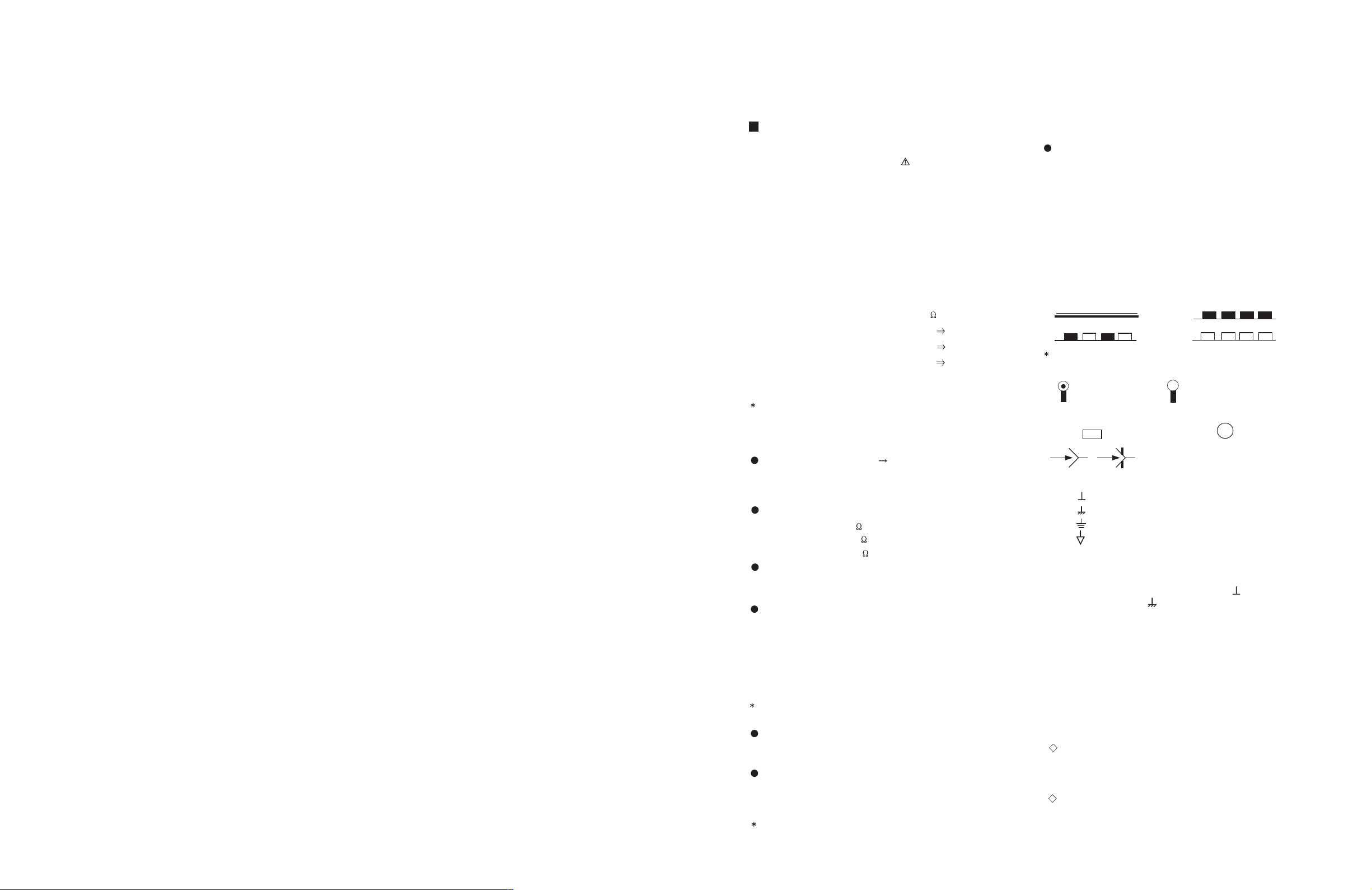
3.INDICATION OF PARTS S YMBOL [EXAMPLE]
In the PW board
:R1209
R209
4.INDICATIONS ON THE CIRCUIT DIAGRAM
(1)Resistors
Resistance value
No unit :[
]
K
:[K
]
M
Rated allowable power
No indication :1/ 16 [W]
Others :As specified
Type
No indication
:Carbon resistor
OMR
:Oxide metal fil m r esistor
MFR
:Metal film resistor
MPR
:Metal plate resistor
UNFR
:Uninflammable resistor
FR
:Fusible resistor
Composition resistor 1/2 [W] is specif ied a s 1/2S or Co mp.
(2)Capacitors
: Original setting position
when shipped
5.NOTE FOR REPAIR ING S ERVI CE
This model's power cir cuit is partly different in the GND. The
difference of the GND is shown by the LIVE : ( ) side GND and the
ISOLATED(NEUTRAL) : ( ) side GND.Therefore, care must be
taken for the following points.
(1)Do not touch the LIVE side GND or the LIVE side GN D and the
ISOLATED(NEUTRAL) side GND simultaneously. If the above
caution is not respected, an electric shock may be caused.
Therefore, make sure that the power cord is surely removed from
the receptacle when, for example, the chassis is pulled out.
(2)Do not short between the LIVE side GND a nd ISOLATED(NEUT RAL)
side GND or never measure with a measuring apparatus measure
with a measuring apparatus ( oscilloscope, etc.) the LIVE side GND
and ISOLATED(NEUTRAL) side GND at the same time.
If the above precaution is not respected , a fuse or any parts will be broken.
Since the circuit diagram is a standard one, the ci rcuit and
circuit constants may be subject to change for i mprovement
without any notice.
NOTE
Due improvement in performance, some part numbers show
in th e ci rcui t diag ram may not ag ree w ith th ose i ndi cate d i n
the part list.
When ordering parts, pl ease use t he numbers t hat appear
in the Pa rts List.
Type
MM
:M eta lized my lar capa ci to r
PP
:Polypropylene capacitor
MPP
:Metalized polypropylene capacitor
MF
:Metal ized film capacitor
TF
:Thin film capacitor
BP
:Bipolar electrolytic capacitor
TAN
:Tantalum capacitor
(3)Coils
No unit
:[
µ
H]
Others
:As specified
(4)Power Supply
:B1
:9V
:5V
Respective voltage values are indicated
(5)Test point
:T est point
:Only test point display
(6)Connecting me thod
:Connector
:Wrapping or soldering
:Receptacle
(7)Ground symbol
:LIVE side ground
:ISOLATED(NEUTRAL) side groun d
:EARTH ground
:DIGITAL ground
:[M ]
Capacitance value
1 or higher :[pF]
less than 1
:[µF]
Withstand voltage
No indication :DC50[V]
Others :DC withstand voltage [V]
AC indicated
:AC withstand voltage [V]
Electrolytic Capacitors
47/50[Example]:Capacitance value [µF]/withstand voltage[V]
No indication
:Ceramic capacitor
:B2 (12V)
AV-N29320
/S/R
AV-N29320
2-12
No.52009
VP0205
DP6060
May 2002 No. 52009
Page 2
AV-N29320
CHANNEL CHART
MODE CHANNEL
TV CATV
BAND
DISP
.
TUNER
BAND
02
03
VL 04
05
06
07
08
09
VH 10
11
12
13
MID
SUPER Q
HYPER
ULTRA
MODE CHANNEL
TUNER
TV CATV
DISP
.
BAND
ULTRA
SUB
MID
14
UHF
69
TOTAL 180CH
VHF 124CH
UHF 56CH
NOTE:
TO RECEIVE THE SUBSCRIPTION OR
PREMIUM PROGRAMMING FROM CERTAIN
CABLE COMPANIES.
SPECIAL ADAPTERS MAY BE REQUIRED.
BAND
14
15
16
17
18
19
20
21
22
23
24
25
26
27
28
29
30
31
32
33
34
35
36
37
38
39
40
41
42
43
44
45
46
47
48
49
50
51
52
53
54
55
56
57
58
59
60
61
62
63
64
65
66
67
68
69
70
71
72
73
74
75
76
77
78
79
80
81
82
83
84
85
86
87
88
89
90
91
92
93
94
100
101
102
103
104
105
106
107
108
109
110
111
112
113
114
115
116
117
118
119
120
121
122
123
124
125
01
96
97
98
99
CONTENTS
AV-N29320
SEMICONDUCTOR SHAPES
BLOCK D IAGRAM
CIRCUIT DIAGRAMS
MAIN PWB CIRCUIT DIAGRA M
MAIN & CRT SOCKET PWB CIRCUIT DIAGRAM
P ATTERN DIAGRAMS
MAIN & CRT SOCKET PWB PATTERN
CHANNEL CHART
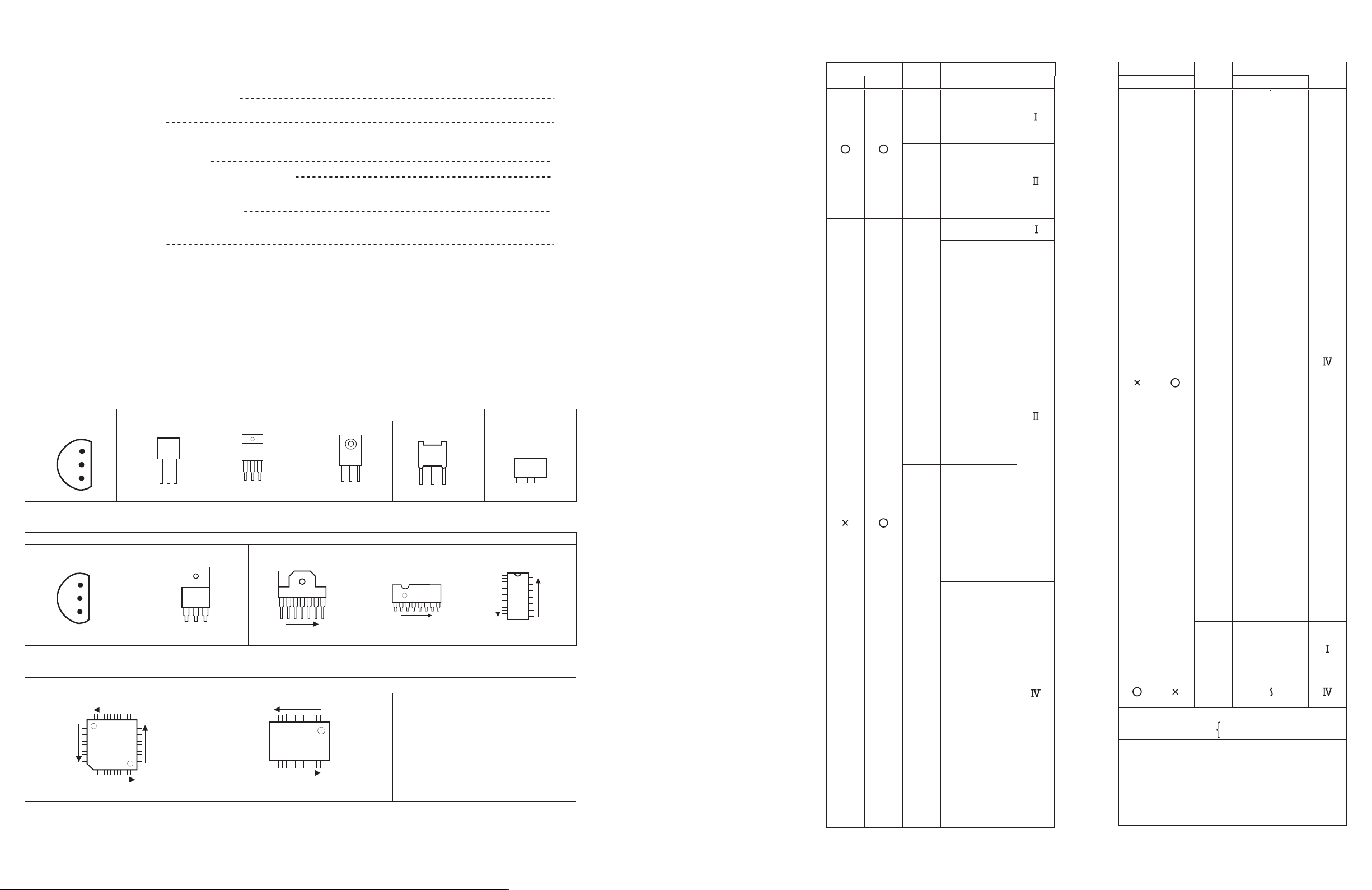
SEMICONDUCTOR SHAPES
TRANSISTOR
BOTTOM VIE W
IC
B O TT OM VI EW F R O NT VIEW TO P VI EW
CHIP IC
2-2
E
C
B
OUT
E
IN
N
N
N
N
1
ECB
IN OUTE
BCE
(G)(D)(S)
FRONT VIEW
1 N
TO P VI EW
ECB
1
N
ECB
1 N
CHIP TR
1
TO P VI EW
C
BE
N
2-2
2-3
2-5
2-7
2-9
2-11
No.52009No.52009
2-11
Page 3

BLOCK DIAGRAM
AV-N29320
AV-N29320
VIDEO
AUDIO
INPUT 1
COMPO-
-NENT
INPUT
AUDIO
OUT
Y
L1
R1
Pb
Pr
L
R
Y/C
Y/Pb/Pr
TU001
TUNER
IF
Y/C
L1/R1
V2
L2/R2
VTV
IC101
IF DET
IC851
AV SW
MPX
IC603
V
Y
C
Y/C OUT
SW
L/R OUT
IC251
Y/C SEP
L/R
Y/C
RM SW
V2
L2
R2
Y
C
R/G/B
L/R
R/G/B
Q301
Q321
CRT
INPUT 2
VIDEO
AUDIO
RGB DRV
CRT SOCKET
PWB
(Within MAIN PWB)
AC IN
MAIN PWB
LF901
D901
IC901
POWER IC
IC702
MEMORY
Y/Pb/Pr
T921
SW.
TRANSF.
IC201
MICOM/V/C/DEF
B1
IC602
AUDIO AMP
L , R
HV
L R
L
SP L
R
SP R
Q521
H.OUT
IC421
VERT OUT
H
V
DY01
T521
HVT
FOCUS
SCREEN
(ITC)
No.52009
2-3 2-4
No.52009
Page 4

CIRCUIT DIAGRAMS MAIN PWB CIRCUIT DIAGRAMS
AV-N29320
AV-N29320
R656
12k
R655
C658
10k
10/50
C657
10/50
4V
1.2V
1.2V
15
14
13
VGR
PLINT
PCINT2
PCINT1
MAIN OUT
MAIN IN
DG GND
SCL
SDA
LSOUT-L
LSOUT-R
BASS-L
TOUT-L
4700p
C677
48
COMP IN
VOLIN-L
4V
IREF
TRE-LNCBASS-R
46474544
0V0V
C676
C656
3.4V
1/50
12
C655
0.012
4V
11
4V
R654
10
100k
C654
R653
1M
5600p
4V
9
N
C653
4.7/50
4V
8
7
R652
100
LOT
ROT
R651
100
W603
QRE141J-101Y
W605
QRE141J-101Y
C652
0.1
C651
4.7/50
4.5V
6
4.5V
5
4V
4
0V
3
0V
2
4V
1
N
SCL0
SDA0
MAIN PWB
D661
MTZJ3.3A-T2
C659
4.7/50
R657
62k
0V
3V 4V 3.8V
17
18
16
NC
GND
SAPTC
IC603
CXA2134AQ-X
TOUT-R
VOLIN-RNCTRE-R
434241
4V
4V
0V
N
C675
0.1
4.7/50
C660
47/25
0V
19
20
NC
VCC
4V4V4V 4V
0V
C674
4700p
C661
0.01
0V 0V
SUB OUT
SURRTC
40
C673
2200p
C662
4.7/50
J007
QNN0282-001
R616
12K
C612
10/50
C131
0.01
AFT
AGC_ADJ
AGC_MUTE
Q001
*4
0V
1
3
R687
220
C687
10/50
D687
*6
ER3
IN
CH1
0V
C616
10/50
C627
47/25
R627
100
Q602
*4
R625
SWITCH
33k
C629
X
R135
1k
1.1V
1.7V
Q131
*1
BUFFER
1.8V
C608
OPT
R_OUTPUT
L_OUTPUT
R605
OPT
IC251 4
1
IC251 17
0.5
IC251 20
1
QSW0619-003Z
C609
C610
OPT
OPT
4.3V4.4V 8.8V
VCC
VREF
L_BOOST
H_BOOST
8
9
8.8V4.3V 8.8V 0V
R607
OPT
R608
X
R606
X
MENU
S756
IC601
GND
BBE
ON_OFF
10
R609
OPT
BBE_SW
IC751
GP1UM281QK
REMOCON
OUT
Vcc
GND
1
2
3
R758
100
C751
47/25
R757
100
C752
X
OPT
REMOCON
BBE
R617
3.3k
R618
3.3k
R615
12K
A_MUTING
C611
10/50
VTV
C607
OPT
F_V
CH+
POWER
R201
2.3V
37
fsc_OUT
Chroma Proc.
C-BPF
NTSC
TINT
Y Proc.
C-Trap
Black stretch
Sharpness
X-RAY
20
R505
150k
0.47
C505
2V
1.5V
2.6V
2.1V
0V
1.6V
2.1V
C272
0.01
0V
0V
S751
QSW0619-003Z
R751
1k
KEY1
22k
1/50
C202
2.4V
36
APC_FIL
Ys
21
C278
C277
R264
0.0015
C203
C276
C274
820
0.01
0.01
C275
0.01
4.7/50
C247
35
APL_FIL
Cb_IN
100
R834
CMP_PB
D353
0.01
X
*5
100k
10k
C354
33
24
100
R836
CMP_PR
R506
470
R263
100
D501
C221
10/50
32
BLACK_DET.
MONITOR_OUT
TV_DVcc
4.2V
MTZJ3.3A-T2
C507
0.01
R507
R359
5.7V
31
ABCL
262725
1.8V
560
K256
BUFFER
V3IN/CIN
C237
0.01
Q281
1.9V2V0V
30
V1_IN
C506
47/25
*1
BUFFER
2.1V
0.01
C241
EHT_IN
Q291
R241
R227
1.4V
34
SVM_OUT
Y_IN
Cr_IN
2322
1.9V 1.8V
100
R835
CMP_Y
K254
QQR0582
-001Z
47/25
180p
C273
0.01
IC201 41
5
SDA1
SCL1
3
IC702
MEMORY
AT24C04-27D303
SDA
SCL
5
67
4.9V
4.9V
*5
RESET IC
2
1
3
R257
2.2k
21
8
IC201
R707
10k
C807
0.01
VDD
4.9V
C701
0.001
56
COMPULINK
10 I/O port
14-bit PWM x1
7-bit PWM x1
8-bit ADC Ext. x3
Remote preprocessor
16-bit int. timerx2
8-bit int. timerx2
Watchdog timer
Interrupt
Ext.x5 Int.x11
IIC bus interface
Ext.x1 Int.x1
AFT2
1
R706
4.7k
R821
120k
C815
0.01
4.2V
R251
3.3k
Q251
*2
3.1V
BUFFER
2.5V
R254
180
R252
R253
10k
1k
4
C663
4.7/50
232221
NOISETC
TVOUT-R
38
R662
100
24
SAPOUT
SAP IN
VEWGT
VETC
VEOUT
VCAIN
VCATC
VCAWGT
AUX1-R
AUX1-L
AUX2-R
AUX2-L
37
4V
R720
821/2W
VE
NC
C664
4.7/50
10.6V
N
4V
25
4V
26
4V
27
2V
28
4V
29
4V
30
1.9V
31
4V
32
4V
33
0V
34
0V
35
0V
36
C665
2700p
C666
0.047
C667
3.3/50
N
C668
4.7/50
C669
10/50
C670
1/50
C671
10/50
C672
10/50
IC704
5V REGULATOR
1
3
C702
10/50
R658
3.3k
R659
3k
R661
3.9k
R664
100
R665
100
AN78L05-T
2
ER3
EL3
R
L
5V
C703
10/50
TM8812CSANG3PF2
D705
R703
10k
IC703
S-80840CNY-T
N
ST IN
TVOUT-L
39
R663
100
AGC
_ADJ
LED
R716
22k
*5
REMOCON
D702
R718
22k
R705
4.7k
4.7k
100
100
R701
4.9V0V4.9V
55
REMOCON
I/O
AFT1
2
1.9V
R714
82k
AFT
R255
1.5k
R704
100
1k
R709
R708
R721
4.9V
1.7V
53 52
54
51
LED
SCL1
SDA1
AGC
ADJUST
ROM:64kB
RAM:2kB
ROM:corre
870X CPU core
Int. x1
STOP/IDLE mode
XO
RESET
KEY
uP_DVSS
8MHzOUT
8MHzIN
4
5
3
6
4.9V 0V
2.2V
R702
100
X701
C709
KEY1
22p
QQR0582-001Z
K255 BW
BW
C253
BUFFER
47p
Q252
*2
2.5V
L251
4.7
C254
C252
180p
100p
IC201 40 IC201 39
4
SDA0
SCL0
R768
6.8k
C716
6V
10/50
4.7k
4.7k
0.01
C712
R734
R733
100
100
R740
100
R732
R731
4.6V
4.5V0V0.2V5V0V
47
50
SCL0
7
C708
K701
OSD R/G/B/Ys/I
Font:16 x 18
Display:32C x 8L
Color:8
Character:256
Half-tone
Transparent
2V
22p
49
SDA0
TEST
8
0V
48
HAZARD
MAIN_POWER
AGC_MUTE
uP_DVDD
9
10
0V
R739
C705
0.01
C704
47/25
QQR0582-001Z
K251
QQR0582-001Z
46
CCD
2.7k
AGC_MUTE
4.2V
1.9V
.47/50
R256
1.5k
K252
BW
Y251
0
K253
QQR0582-001Z
SDA0
SCL0
SCL0
1.4V
C711
uP_AVdd
uP_VVSS
0V 0V
K702
47/25
C265
C266
0.01
C267
0.01
C269
0.01
K257
C261
C262
C263
C264
R769
1k
Q701
*1
1.3V
R770
10k
47/25
0V
45
44
TV_AGND
uP_AGND
Hor. proc.
Sync. sepa
Hor. VCO HAFC-1
HAFC-2 H-shift
TV_HGND
FBP_SCP
131211
0.8V
R501
4.7k
FBP
0.01
0.01
0.01
C268
47/25
C270
47/25
R261
100
R262
100
X
5
D367
*5
D366
*5
D365
*5
X
0.01
47/25
0
R363
C362
C361
R360
8.7V
2.3V
41
43 42
IK_IN
B_OUT
Cut-off Drive
RGB_Vcc
RGB switch
Brightness
Half-tone
Transparent
Base Band Proc.
Int/Ext switch
Color Uni-color
RGB Matrix
0V
HAFC_1
HOUT
H_Vcc
15
14
16 17
8.8V
1.8V
6.4V3V3.8V 0V 1.8V
2.2/50
C504
X
680
R502
R504
3.9K
R503
HD
C502
C501
0.01
47/25
IC251
TC90A49P
4.2V
1
VDD2 YOUT
1.2V
BIAS
2
2.5V
VRT
3
2V
VIN
4
1.5V
5
VRB
4.2V
6
VDD3
0V
VSS2
7
4.2V
VDD4
8
4.6V
9
SDA
4.5V
10
SCL
G
100R366
XR362
C503
R
2.2V 2.5V
40
G_OUT
AKB
Vsaw
0.01
B
9V
100
100
R365
R364
X
R361
39
R_OUT
Vert. proc.
V.C /D
V.r am p
V.geometry
V.D ri ve
VOUT
18
R401
0.47
C401
V-OUT
C402
1000p
DAVRB
DAVRT
COUT
VSS1
VDD1
APCFIL
FSC
KILLER
TEST
GND
47/25
C243
1k
CN00T
D370
*5
D369
*5
D368
*5
38
YC_Vcc
EW_OUT
19
18
16
14
12
11
0.01
C244
20
19
17
4.2V
15
13
LED
29
28
2.1V
C222
R282
2.2k
2V
R292
2.2k
*1
YC_GND
V2_IN/Y_IN
0.1
2.6V
2.7V
R293
Q751
*3
R756
1.2k
D751
SLR-342VR3F
RED
(LED HOLDER:LC30190-001B-A)
0.5
0.8
R290
1K
C282
X
R284
R283
X
820
L281
QQL244K
C281
-150Z
X
C292
X
R294
470
L291
QQL244K
C291
-150Z
X
IC201 26
IC201 28
IC201 14
5
IC201 18
2
R299
C295
Cout
X
1K
0.01
C283
33p
BUFFER
C293
15p
QSW0619-003Z
R289
1K
C285
R280
47/25
1K
Yout
Q283
R285
330
4.2V
2.6V
Q282
*2
BUFFER
2V
R287
R286
1K
1k
R295
330
Q292
4.2V
*2
Q293
2.7V
2V
R297
R296
1k
VOL-
VOL+
S753
S752
QSW0619-003Z
R753
R752
1.5k
1k
ROT
LOT
C615
C602
OPT
4.3V 4.3V
20 19 18 1617 15 14 13 12 11
R_INPUT
L_INPUT
1
4.3V 4.3V
N
C601
OPT
C613
X
Q352
8.7V
5.2V
R356
C352
12k
47/25
R288
0
*1
AMP
C284
X
R298
C294
0
X
*1
AMP
1K
X
R602
N
HPF_R
HPF_L
2
R601
BUFFER
*2
OPT
OPT
S754
QSW0619-003Z
R754
2.7k
Y602
0
C604
OPT
4.3V 4.3V 4.3V
CR1_R
CR1_L
4.3V 4.3V 4.3V
C603
OPT
Y601
5.8V
R604
OPT
BPF_R
BPF_L
R603
0
OPT
D352
*6
C606
OPT
CR_R
CR2_L
543
C605
OPT
R354
330
CH-
S755
QSW0619-003Z
R755
5.6k
4.3V
LPF_R
LPF_L
67
4.3V
J006
QNN0281-002
2
R688
220
C688
10/50
IC602
MUTE
2
16
.8V
R134
680
R133
820
IC101
M52342SP
IFDET
R117
27k
2
1
D688
*6
EL3
C804
10/50
LA4446!AUDIO
LNF
POGND
3
4
1V
0V 15
C617
220/16
R619
390
100/16
QRL039J-100
QRX029J-3R3
L131
QQL244K-220Z
QAX0639-001Z
150k
R112
150k
J005
QNN0281-003
R805
100
LBS
5
.7V
C618
CF131
C121
X
L114
R119
R111
R115
100
R113
100
C113
0.01
4
6
POGND
101
0V 1V 0V
A_GND
47/25
C117
1617
VREG.OUT
VIFIN
1
R628
OPT
RNF
Y605
BW
C623
220/16
R620
390
T111
4V
VCOCOIL
VIFIN
3
2
127
4.1V 4.7V
151413 12 1120 19
VCOCOIL
GND
GND
0V 0V
R629
OPT
PRGND
C625
470/16
R164
0.01C107
VCC
QIFDETIN
7
13IN11
1k
47/25C106
5
8
CH2
0V
C116
9
C622
10/50
C163
47p
2.2V 3.1V
QIFOUT
IFAGCFILTER
2.4V 2V
0.22
C161
10/50
J008
OPT
Y603
BW
Y604
BW
C619
470/16
C620
R621
QAX0642-001Z
CF161
C164
47p
L161
QQL244K-220Z
22K
10K
R171
R163
LIMITERINAUDIOOUT
AFTSW/NPSW
NFB
109867554433221
3.3k
R161
!
CEBSS09D-03KJ2
STEREO
SP01
L
1
2
3
4
SP02
A_VCC
A_GND
V-OU T
FBP
R
A_VCC
A_GND
V-OU T
HD
HD
FBP
ABCL
MAIN_PW
9V
CN00S
S
QGA2501C5-04Z
0.1
4.7
C626
0.1
R622
4.7
R167
R165
1K
22K
Q161
*2
BUFFER
R166
R168
10K
100
R169
560
C165
0.01
Y161
X
C166
0.01
2V
IC101 18
2
4.4V
C162
10/50
VLR
2
1
R804
75
D804
*6
OUT
OUT
CH1
CH2
RBS
Vcc
6
8
9
8.8V
8.8V
16
15
.8V
.7V
C624
100/16
C614
470/16
R614
W602
A_VCC
R132
220
R131
1k
QQR0907-001
C119
680p
0.01
.47/50
C118
C120
X
R116
68
X
2.1V 4.9V
1.5V
3.5V
18
EQF/B
VIDEOOUT
APCFILTER
RFAGCOUT
AFTOUT
RFAGCDELAY
1.7V
5.6V
1.7V 1.3V 1.4V
C114
C124
0.01
0.01
SFE-1010A-M2
[AV-N29320/S]
SFE-1011A-M2
[AV-N29320/R]
1
R101
5.6k
QAX0349-001
C101
0.01
R008
82
K001
C004
220/10
SF101
F072FPL
!
TU001
QAU0275-001
CF001
0V
IF
33.1V
C003
47/25
R005
0
R006
22k
BT
C005
0.01
4.2V
5V
C002
0.01
C006
4.6V
X
SDA
R004
4.4V
220
SCL
R003
4.2V
220
ADRS
C007
X
1.8V
AGC
C001
4.7/50
QQR0582-001Z
NOTE
*1
:
:
*3
:
*4
:
*5
:
*6
:
*7
:
*8
:
*9
:
K101
2SA1037AK/QR/-X
2SC2412K/QR/-X
DTA124EKA-X
DTC124EKA-X
1SS133-T2
MTZJ9.1C-T2
MTZJ5.6A-T2
RGP10J-5025-T3
1SR35-400A-T2
OR
OR
2SB709A/QR/-X
2SD601A/QR/-X
BW
X
0
*
:
BUS WIRE
:
NON-MOUNT(OPEN)
:
SAFETY PARTS
:*20 RESISTOR
Ω
DIFFERENCE
:
BT
PART S
5V
STBVCC
BBE_SW
IC851 10 38
1
0.1V
IC851 34
0.5
IC851 36
1
FIX_L
FIX_R
VOUT2
LOUT2
1
IC851
TA1218AN
Y852
5
TOUT2
2
X
No.52009 No.52009
L
R
Yout
Cout
47/25
V1
36
YOUT
VINTV
V1
3.6V
7
C851
0.01
3.8V 3.6V
35
ROUT1
LINV1
8
C852
0.01
34
COUT
RINV1
9
10/50
0.01
C861
C860
8.7V 5V 5V 5V 5V
32
33
CIN
VCC
VINV1
LINS1
11
10
5V
5V 5V 5V
C853
C854
0.01
VTV
R778
10k
C862
10/50
3.3V 3.8V
37
40 39
38
LOUT1
VOUT1
LOUTTV
ROUTTV
DET_IN
DET_SELECT
LINTV
RINTV
5
4
6
3
5V 5V 5V 5V
R851
R852
R853
100
100
100
EL1
ER1
0.01
C859
0.01
C858
31
RINV2
Y/VINS1
12
C855
R854
0.01
100
R855
15K
Y1
Y851
0
F_V
100
0.01
C857
C856
R861
10/50
5V 0V 4.6V
27
29
304142
28
YIN
LINV2
VINV2
ADDRESS
RINS1
CINS1
LINS2
Y/VINS2
14
15
13
16
5V 1.7V 5V 5V 5V
OPTR858
OPT
R859
R856
100
.01
C864
EL2
C1
26
SYNC_OUT
RINS2
17
OPT
R860
.01
C863
CMP_Y2
100
100
R776
R777
R775
10k
4.6V 0V
4.2V
22
25
23
24
SCL
SDA
GND
CINS2
I/01
I/02
I/03 I/04
21
20
19
18
4.2V 0V 0V
1.7V
15k
R771
C865
ER2
R774
10k
R772
R773
10k
10k
.01
R862
A_MUTING
R857
10k
Q851
SWITCH
100k
*1
R863
47k
FIX_L
FIX_R
R683
R685
22K
SWITCH
22K
Q681
Q682
*1
SWITCH
C681
10/50
D681
R691
*6
C682
10/50
D682
*6
Q683
Q684
*1
SWITCH
SWITCH
C1
D803
*6
C803
1/50
R684
R803
22K
J002
*2
QNN0348-001
R681
220
1
4
82K
2
R682
220
R692
22K
R686
22K
*2
D807
J001
QNZ0531-001
10 9
75
87
2
VIDEO
L
3
R
5
Y855
X
Y1
V1
ER1
EL1
D801
*6
*6
C801
10/50
R801
68
C802
1
10/50
R802
75
3
6
C683
10/50
Y
4
C684
10/50
J003
QNN0349-002
2
D802
*6
5
D683
*6
D684
*6
CMP_Y2
C834
D834
*6
10/50
C831
0.1
1
3
6
4
CMP_Y
D831
R831
*6
75
C832
0.1
CMP_PB
D832
R832
*6
75
C833
0.1
CMP_PR
D833
R833
*6
75
EL2
ER2
D686
D685
*6
*6
Y852
X
C686
C685
10/50
10/50
L
4
R
J004
OPT
Y856
X
Y854
0
CN00C
QGA2501F1-06
QQLZ014-R39
L101
R103
QRE121J
-101Y
C104
0.01
Q101
2SC5083/
L-P/-T
0.7V
1.6V
C105
0.01
8.7V
R104
18
R102
C102
1.8k
0.01
R105
27
QQR0582-001Z
SCL0
SDA0
SCL1
SDA1
470
470
470
470
R765
R764
R766
R767
2211334
56
SDA0
SCL0
2-5 2-6
Page 5

MAIN & CRT SOCKET PWB CIRCUIT DIAGRAM
AV-N29320
AV-N29320
CN0PW
QMPD390-200-JS
POWER CORD
AC120V
60HZ
L01
DEG. COIL.
CE41329-00DJB
CNDEG
QGA7901C1-02
NOTE
*1
2SA1037AK/QR/-X BUS WIRE
:
*2
:
2SC2412K/QR/-X
DTA124EKA-X
*3
:
*4
DTC124EKA-X
:
*5
:
1SS133-T2
*6 MTZJ9.1C-T2
:
MTZJ5.6A-T2
*7
:
:
*8
RGP10J-5025-T3
*9
1SR35-400A-T2
:
F901
QMF51N1-5R0-J5
125V
5.0A
DEG
2
1
PW
2
1
IC901
STR-G5624/F8
ERZV10V621CS
QRZ9041-275
.22 2W
QRT029J-R22
K903
POWER IC
1
D907
2
3
4
5
R904
R991
BW
X
C910
470p
CH
VA901
R908
QRK126J-681X
D908
BW
:
X
:
:
0
:
*
1N4003-T2or
C901
.1 AC275V
QFZ9072-104 QFZ9072-104
231
QQR0527-003
C904
.001 AC250V
QCZ9054-102
TH901
QAD0129-3R0
R901
UNFR .47 7W
QRF074K-R47
R905
.22 2W
QRT029J
-R22
K904
BW
QQR0582-001Z
K901
K902
QQR0582-001Z
D904
R907
*8
4.7K
C909
1000p
CH
47/50
MTZJ15C-T2
NON-MOUNT(OPEN)
SAFETY PARTS
0 RESISTOR
Ω
:
DIFFERENCE PARTS
C902
.1 AC275V
4
LF901
GSIB460-S1
.001 AC250V
QCZ9054-102
C903
QEZ0169-477
C908
QCZ0340-102
C911
*
R902
47K
1/2W
SARS01-T2
R903
47K
1/2W
D902
*8
1/2W
D903
*8
C907
D906
X
D901
C905
D905
LIVE
( )
QQT0355-001
.01 AC250V
QCZ9074-103
QQS0158-001
R910
680K
1/2W
R911
47
1W
R906
2.2
1/2W
T901
D922
*9
RELAY
RY901
QSK0085-001
1
2
34
C922
100/16
0.1V
C991
T921
D921
*9
D924
D923
*9
D925
*5
R921
10
1/2W
QRE121J
-100Y
SWITCH
0.6V
Q921
2SD1383K/AB/-X
C992
.01 AC250V
QCZ9074-103
K921
QQR0582-001Z
K924
QQR0582-001Z
QCB32HK-102Z
K922
QQR0582-001Z
R925
1 1W
QRX01GJ-1R0
K923
QQR0582-001Z
ISOLATED
( )
MAIN PWB
SFE-1010A-M2
SFE-1011A-M2
C921
*9
470/25
R934
27K
R933
10.6V
D931
*5
Q922
2SC2785/JH/-T
CN0B1
123
D926
RU3AM-LFC4
L921
QQL26AK-470Z
C923
QEZ0203-107
1 1W
L922
QQL26AK-470Z
C925
470/16
C927
470/16
C946
0.01
12K
R935
R922
4.7K
R923
47K
C929
QCZ0340-102
C930
QRX01GJ-1R0
D927
RU3YX-LFC4
C931
QCB32HK-102Z
D928
RU3YX-LFC4
CH41169-R03Y
R924
10.7V
0V
33K
C926
100/16
[AV-N29320/S]
[AV-N29320/R]
10.7V
Q923
*1
0V
R932
12K
C935
R938
10K
1/2W
47/16
R939
10K
1/2W
R937
X
133.6V
133.2V
Q924
R929
2SA1208/ST/Z1-T
22K
1/2W
R930
47K
1/2W
C924
47/160
11.4V
1
IC921
AN7809F
C940
0.01
REGULATOR
R936
10K
1/2W
100/6.3
D929
C933
47/10
18R941 2WOMR
3
R926
C932
X
R926,R927
1.2
2
9V
100/16
[1/2]
R927
R928
2.7K
2W
C943
0.01
C941
D933
1N4002G-T2
D932
MTZJ33B-T2
1/2W
D930
R931
X
QRT029J-1R2
8.8V
R942
5.6
1/2W
C942
100/16
STBVCC
STB-GND
B1
MAIN_PW
IC922
AN7805F
REGULATOR
5.9V
Q301 C
130
R302
12K
2WOMR
170.5V
6
5
1
2
3
4
1
3
2.3V
R304
10K
2WOMR
2.6V
R314
10K
2WOMR
2.2V
R324
10K
CN0HV
V
CN00U
HB
R312
12K
R322
12K
1.9V
2.2V
18V
DEF. Y OKE
!
U
HEATER
DEF. Y OKE
!
Q301
2SC4544-LB
B.OUT
R305
330
1.5k
161.4V
Q311
2SC4544-LB
R.OUT
R315
330
175.3V
Q321
2SC4544-LB
G.OUT
R325
330
DY01
DY01
150
Q311 C
C331
D331
X
R331
X
R332
Q331
X
X
R333
R301
150
C301
Q332
X
X
X
X
Q321 C
120
C341
47/25
MAIN
PWB
CN10T
T
GND
5
4
9V
3
B
G
R
CRT SOCKET
QRE121J-681Y
C409
C410
R411
12k
C412
2.2/50
X
QCB32HK-102Z
R526
R527
!
QRX01GJ-1R0
1 1W
L522
QQLZ026-880
D521
1SR35-400A-T2
[2/2]
IC421 3 6
30
R407
C411
2200/35
R409
QRX01GJ-1R0
C532
D522
RH1S-T3
FOCUS
SCREEN
DEFFERENCE LIST
SFE-1010A-M2 SFE-1011A-M2
A68QDN891X001V01 A68ADT25X881
.01 400V
C911
QFP32GJ-103Z
OPT
IC421 AN5522! V.OUT
PWB
SFE-1010A-M2
SFE-1011A-M2
IC421 5
60
UPPUMP
4
5
0V
C413
X
C407
100/35
R528
QRE121J-472Y
C531
D524
-1R5
R523
QRL039J-152
QRE121J-184Y
12
.1V
D402
D401
*9
D523
QCB32HK
RGP10J
-5025-T3
R525
AMP
6
2.8V
MTZJ75-T2
R414
10K
1SR35-400A-T2
-102Z
QEZ0203-107
711223
3.2V
C406
1000p
K401
QQR0582-001Z
R415
X
T521
!
QQH0129-001
8
7
6
10
9
C525
R541
QRE121J-683Y
R524
220K 1/2W
QFLC2AK-104Z
R413
X
R412
15K
3
2
1
QFLC2AK-104Z
R410
QRK129J-150
C526
0.082
MY
or RGP10J-5025-T3
BT
5V
4.2V
C945
0.01
GND
A_VCC
A_GND
ABCL
9V
BT-GND
82R943 1/2W
5V
1
2
3
C944
100/16
HD-GND
HD
FBP
FBP-GND
Q501 B
1
2SC4212/Z1/
0.2V
R508
100
R509
270
Y501
Q501
0
V-GND
VP
V-OUT
Q501 C
200
QRE121J-103Y
64.9V
C508
QCB32HK
R535
-151Z
VP-GND
X
R510
QCB32HK
R403
10k
R404
X
R405
10k
D526
MA4068N/Z1/-T2
R534
R511
1.8K 2W
R512
1.8K 2W
CE42034-002
1
3
C510
2.2/250
C509
-331Z
X
T501
R406
4
X
5
C403
10/16
N
123
!
!
R533
2.94K 1/10W
NRZ0032-2914X
Q521
2SD2634-YD
-0.1V
R521
QRE121J
-220Y
Q521 B
2
C405
10/50
R402
4.7K
CNHHS
R532
X
R531
7.15K 1/10W
NRZ0032-7151X
C521
OPT
.013 1.5KVH
QFZ0198-133
D525
C522
MPP
2200P
*7
!
3.2V
C408
10P
C404
47/35
C529
L521
QQR1027-004
QCB32HK-561Z
OPTY521
OPTY522
.62 250V
QFZ0197-624
27
.2V
R529
QRK126J-4R7X
C530
QFLC2AJ-103Z
!
R530
C528
470/35
C524
R522
!
C523
MPP
1.8V
1.5 2W
QRX029J
QRE121J-681Y
R311
150
C311
X
R321
150
C321
Y341
X
(Within MAIN PWB ASS'Y)
R408
QRE121J-681Y
R416
QRE121J-102Y
S401
QSL4A13-C02
C527
10/250
EHT
FOCUS
SCREEN
CN0HV
H
R303
1.5k1/2W
C302
330p5
R313
1/2W
R323
1.5k
1/2W
C322X
(ITC)
(ITC)
270p5
(V)
(H)
270p5C312
R306
100
R316
100
R326
100
CRT SOCKET
SK351
!
QNZ0537-001
BK
L341
C342
X
NC
123
4
11
RK
8
GK
6
H
10
9
Y342
X
TP-E
QQL03BJ-390Z
CN10U
U
23
28
7
250
10
1200
V01
*
B
R
G
G1 G2 G3
412 571
Y343
X
!
C343
0.001
3KV
QCZ0121-102
T521
100
8
60
E1
No.52009
2-7 2-8
No.52009
Page 6

PATTERN DIAGRAMS MAIN PWB PATTERN
E
MARK
E
C
B
B
C
5
1
T
C311
C312
C321
C331
C341
Y341
W351
L341
Q311
R302
R306
R314
R315
R316
R321
R323
R331
R332
Y342
TP-E
W412
MARK
TP-R
E
BK
H
HE
RK
G2
G1
GK
C
E
B
1
4
E1
U
Q321
C301
C302
C322
C343
D331
Q331
Q332
R301
R304
R305
R311
R322
R324
R325
R326
R333
C342
Y343
W352
SK351
SCREEN
Q301
C
KF1662
/2!
0
R
3
0
3
R
3
1
2
R
3
1
3
UL MARK
MLKJIH
9
9
C909
R907
8
8
7
7
6
6
5
5
4
4
3
D904
R908
C910
IC901
D908
3
1
K901
K902
C903
W901
C904
R901
LF901
C901
VA901
CL003
2
2
WHT
1
0
D901
125V 5A
45
2
C991
C905
C902
F901
CL002
HS009
R991
D903
D902
W903
D907
S751
R904
R906
W902
D906
C907
K903
K904
D905
C908
R911
R905
R910
C911
C992
R937
W905
W904
DEG
R934
Q923
R932 R933
Q922
R935
C935
D930
D929
W918
PW
C682
C681
D681
POWER
L
W911
R931
C672
2
1
C932
RY901
TH901
W912
R661
R921
R662
R663
T901
C922
D931
C671
D682
L131
R501
C244
C247
D369
D368
D370
R860
R117
C124
C120
C121
R111
W831
C203
R625
C607
C118
R603
R604
C609
MENUCH -CH +
AV-N29320
FEDCBA
R006
R005
C007
C006
C002
C005
R008
W833
R241
BT
IF
C853
1
20
CF131
W254
W272
C507
R227
2935
R359
C202
R102
R119
C354
Q602
C629
C605
C606
C102
CF001
R112
R134
W835
W255
W291
D501
C241
TU001
AGC
ADRS
R003
SCL
SDA
5V
R105
C101
R113R115
R116
W111
W281
C506
R201
C221
R627
R605
R607
R004
R936
R101
C104
T111
R133
R354
W206
D353
C627
2
F
1
SF101
5
R161
R171
R164
Q131
C131
R135
W834
C616
C001
C004
C003
Q101
L161
W954
W207
R356
R614
D687
C687
1
R103
L101
C107
C163
W953
Q352
6
D932
C161
C116
11
C164
D352
C352
3
C
NC
R104
W102
10
C166
R163
W963
SDA2
C162
K101
W962
W952
Y605
R618
R615
R687
SCL2
C105
IC101
CF161
W101
W705
W951
R620
C106
R167
W104
W704
W961
R506
R619
D688
C688
1
2
J006J007
SDA1
R939
R938
K001
W703
R507
SCL1
Y161
R165
C622
GND
R767
R166
R169
C165
W103
C617
C614
C623
R688
1
1
R766
W702
R765
R530
Q161
R168
H602
1
5
10
13
R805
R764
C528
W701
IC602
J005
E
S401
C804
C531
D524
R528
C618
W401
D401
W404
W353
2
4
1
W403
C530
D525
C624
R622
D804
1
U
W505
C626
R804
24.FEB.02
W506
R
409
R404 R405
R403
R406
HS004
W409
R942
R621
C619
C625
W622
J008
JIM
R402
C405
1
4
R410
R413
C404
IC421
C406
C403
W507
W405
C620
Y604
5
6
7
C412
426
W406
C942
Y603
14
R628
R629
2
96
D
5
GND
28V
R415
35 71
W408
GND
IC922
R943
W621
8
Heater
8
C407
3
7
CKF1662-BU1-1
4
NC
FBP B1
R416
R414
R412
R411
C408
K401
W402
C413
W407
C945
5V9V
2
1
0
/2!
UL MARK
23
1
ABLNCHB
T521
COL
910
C411
D402
R407
R408
C409
C944
CA
D522
C522
L521
Y521
Y522
C410
R508 R509
C521
H002
C524
Q501
TOP
AV-N29320
JKLM
31
8
7
6
5
4
3
Q924
R929
C669
C670
C673
POWER
D751
K
R928
C668
C666
Q921
C674
C675
R903
R902
T921
R926
D923
D924
D925
W909
W908
R923
R922
C665
R659
C667
30
35
40
45
C676
C677
R756
25
IC751
3
10
11
12
13
14
15
16
D922
D933
R658
48
C651
W920
9
K921
C924
C664
R927
2
R941
C752
K924
C923
R930
W917
W928
W927
W926
W923
W922
W925
W924
C663
1
K923
1
C652
B1
C929
20
C751
R925
K922
L921
D921
IC921
W907
C941
C943
C662
15
5
IN
W910
C661
IC603
10
C654
R924
C660
R653
R757
D927D928
C921
W803
W611
C659
R657
R758
D926
C933
C926
C940
OUT
W202
W614
R655
Q751
C925
L922
GND
W201
C658
R656
W919
C927
C930
C946
W804
W814
C703
W713
R664
C656
C655
R654
C653
R652
R651
R254
C702
C657
Q682
Q683
Q681
R685
R252
R720
R665
C931
R682
R692
Q684
Q251
IC704
VOL +
R684
R257
R251
W718
S752
R686
C294
R706
W717
W607
R691
C252
R255
C254
R256
W711
C701
W608
W609
W610
2
J002
W251
W813
W613
W716
3
R681
R683
D807
W681
Q851
R863
R862
R852
C253
K254
W811
IC703
D705
W715
W719
W942
W941
W601
W602
W604
W916
W915
C684
W810
W709
W603
W605
D684
D803
R253
K255
K256
R702
R701
R721
W732
W710
4
R295
R292
W205
1
W815
C859
R298
Q293
C862
R263
W253
R714
C815
R821
W714
5
24
1
R803
8
J001
C803
15
W812
R296R297
Q292
R293
R294
L251
Q252
C276
C274
Y251
R261
R262
W204
W203
C704
C711
IC201
1
C807
IC702
W612
R751
R752
Y854Y855
D683
314
R802
IC851
C292
Q291
C266
C602
2
6
J004
3
9
R801
C293
C291
C273
X701
C705
R707
50
4
58
C860
C270
K253
C613
C615
D802
R853
C851
C858
R264
K701
R705
C716
R716
W913
7
W271
C272
C709
R718
R708
W914
R753
W801
10
35
C708
R704
R731
IC601
S754S753
C802
R854
C852
W808
L291
C268
R739
R733
D702
R732
C683
W802
R857
C854
C861
C275
C267
R734
R740
Y601
R601
1
R602
Y602
510
K702
20
C855
45
R768
C801
R855
W809
C265
W707
C502
R503
C712
Q701
R769
W256
W501
R770
121110
W805
R851
R861
R778
402242
K257
11 15
C269
15 10
R703
56
R709
C601
VOL -
Y852
C864C865
C361
No.52009 No.52009
G
254
6
R831
1
R833
D686
J003
Y856
C686
C833
D832
D685
C831
D801
W836
Y851
C863
W807
C857
IC251
K252
W252
R504
R360
40
C362
W361
D834
C685
R771
C856
30
20
C263
C264
1
K251
C501
W706
R363
R366
D366
D365
D367
W362
C612
C611
S755
R754 R755
D831
Q001
C834
W131
15
R856
21
R773
R772
R774
R776
R777
25
W132
R287
R285
C284
Q282
Q283
R286
C283
R288
L281
C282
C281
R283
R284
R282
C278
Q281
C277
C261
C262
R834
R835
W708
W112
W113
R502
C401
C504
R401
251520
C503
R505
C505
R361
R362
R364
R365
C243
51
R616
R617
R608
R606
R609
105
C610
15
C608
GHI J
W001
R858
R775
W002
C119
R132
C402
11
S756
2-9 2-10
R832
3
D833
C832
R859
C113
C117
L114
R131
R836
W832
C603
C604
C114
C237
C222
C527
R522
Y501
B
R526
C523
C532
C509
C508
R523
T501
D523
R525
Q521
R521
L522
W503
R510
R529
R527
W509
R524
W502
C529
C525
R534
R531
D526
R541
W504
C510
X
R535
W508
D521
C526
W510
R533
R532
R511
R512
1
3
9
8
7
TP-91
6
5
4
3 3
TP-E
FRONT
TP-E
(B1)
CRT SOCKET
PWB PATTERN
 Loading...