

Page 1
SCHEMATIC DIAGRAMS
COLOR TELEVISION
52104200304
BASIC CHASSIS
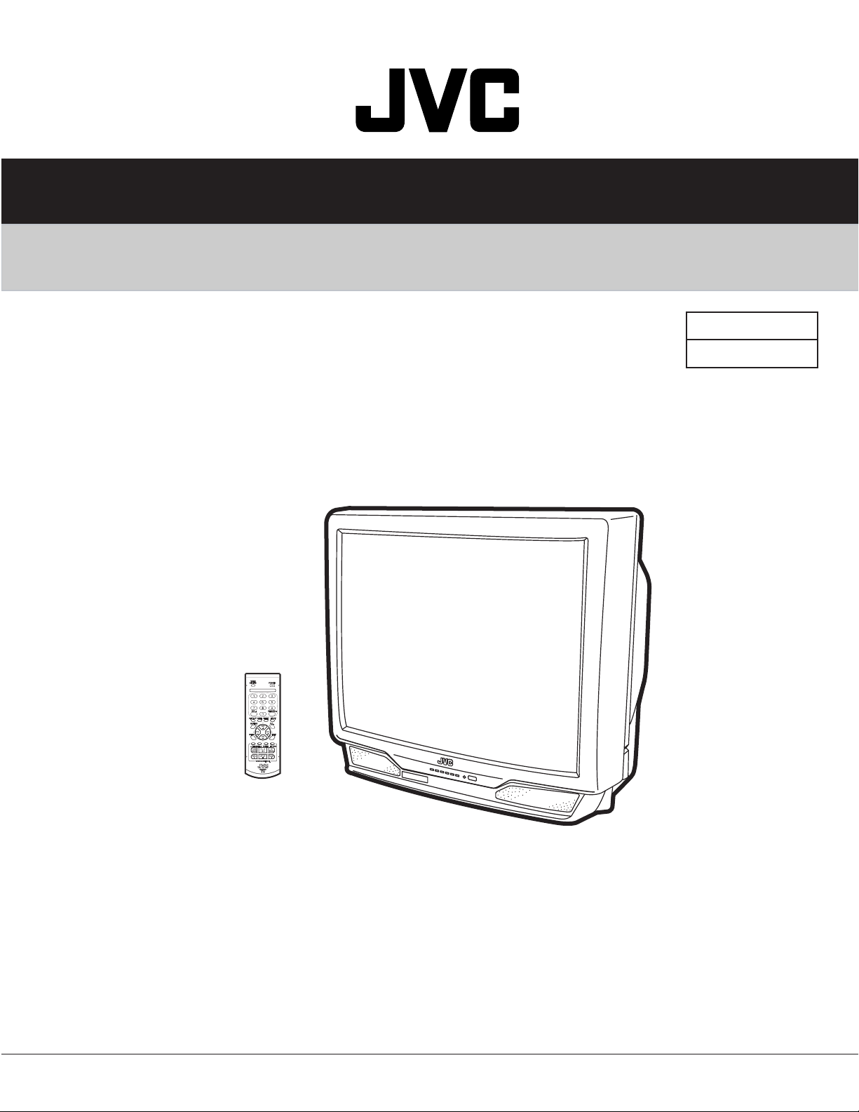
AV-32430/M, AV-32432/M,
AV-32430/R, AV-32432/R,
AV-32430/Y, AV-32432/Y
AV-32430
AV-32432
GE2
CD-ROM No.SML200306
COPYRIGHT © 2003 VICTOR COMPANY OF JAPAN, LTD.
No.52104
2003/04
Page 2
A V-32430
A V-32432
AV-32430/MA, AV-32430/RA, AV-32430/YA
AV-32432/MA, AV-32432/RA, AV-32432/YA
STANDARD CIRCUIT DIAGRAM
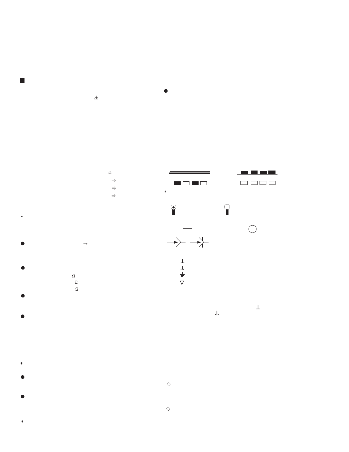
NOTE ON USING CIRCUIT DIAGRAMS
1.SAFETY
The components identified by the symbol and shading are
critical for safety. For continued safety replace safety critical
components only with manufac tures recommended parts.
2.SPECIFIED VOLTAGE AND WAVEFORM VALUES
The voltage and waveform values have been measured under the
following condit ions.
(1)Input signal : Co lour bar signal
(2)Setting positions of
each knob/button and
variable resistor
(3)Internal resistance of tester
(4)Oscilloscope sweeping time
(5)Voltage values
Since the vol tage values o f signal cir cuit vary to some extent
according to adjustments, use them as reference values.
: Original setting position
when shipped
:DC 20k
:H
:V
:Others
:All DC voltage values
/V
20µs/div
5ms/div
Sweeping time is
specified
3.INDICATION OF PARTS SYMBOL [EXAMPLE]
In the PW board
:R1209
R209
Type
No indication
MM
PP
MPP
MF
TF
BP
TAN
(3) Coils
No unit
Others
(4)Power Supply
Respective voltage values are indicated
(5) Tes t po i nt
:T est point
(6)Connecting method
:Ceramic capacitor
:M etal ized my lar cap ac i tor
:Polypropylen e ca pacitor
:Metalized polypropylene capacitor
:Metal ized film capacitor
:Thin film capacitor
:Bipolar electrolytic capacitor
:Tantalum capacitor
µ
:[
H]
:As specified
:B1
:9V
:Only test point display
:Connector
:Receptacle
:Wrapping or soldering
:B2 (12V)
:5V
4.INDICATIONS ON THE CIRCUIT DIAGRAM
(1)Resistors
Resistance value
No unit :[
K
M
Rated allowable power
No indication :1/ 16 [W]
Others :As specified
Type
No indication
OMR
MFR
MPR
UNFR
FR
Composition resistor 1/2 [W] is specified as 1/2S or Comp.
(2) Ca pa citors
Capacitance value
1 or higher :[pF]
less than 1
Withstand voltage
No indication :DC50[V]
Others :DC withstand voltage [V]
AC indicated
Electrolytic Capacitors
47/50[Example]:Capacitance value [µF]/withstand voltage[V]
]
]
:[ k
:[M ]
:Carbon resistor
:Oxide metal film resistor
:Metal film resistor
:Metal plate resistor
:Uninflammable resistor
:Fusible resistor
:[µF]
:AC withstand voltage [V]
(7)Ground symbol
:LIVE side ground
:ISOLA TED( NEUTRAL) side ground
:EARTH ground
:DIGITAL ground
5.NOTE FOR REPAIRING SERVI CE
This mode l's p ower circu it is p artly diff erent in the GND. The
difference of the GND is shown by the LIVE : ( ) side GND and the
ISOLATED(NEUTRAL) : ( ) side GND.Therefore, care must be
taken for the following points.
(1)Do not touch the LIVE side GND or the LIVE side GND and the
ISOLATED(NEUTRAL) side GND simultaneously. If the above
caution is not respected, an electric shock may be caused.
Therefore, make sure that the power cord is surely removed from
the receptacle when, for example, the chassis is pulled out.
(2)Do not short between the LIVE side GND and ISOLATED(NEUTRAL )
side GND or never measure with a measuring apparatus measure
with a measuring apparatus ( oscilloscope, etc.) the LIVE side GND
and ISOLATED(NEUTRAL) side GND at the same time.
If the above precaution is not respected , a fuse or any parts will be broken.
Since the circuit diagram is a standard one, the circuit and
circuit constants may be subject to change for improvement
without any notice.
NOTE
Due improvement in performance, some part numbers show
in th e circui t diag ram may not agree wi th those i ndi cate d in
the part list.
When ordering parts, please use the numbers that appear
in th e Parts List .
2-1
No.52104
Page 3
A V-32430
A V-32432
CONTENTS
SEMICONDUCTOR SHAPES ......................................................................2-2
BLOCK DIAGRAM........................................................................................2-3
CIRCUIT DIAGRAMS....................................................................................2-5
MAIN PWB CIRCUIT DIAGRAM ................................................................................................................ 2-5
AV SELECTOR PWB CIRCUIT DIAGRAM ................................................................................................. 2-9
CRT SOCKET PWB CIRCUIT DIAGRAM..................................................................................................2-11
FRONT CONTROL PWB CIRCUIT DIAGRAM ......................................................................................... 2-13
FRONT TERMINAL PWB CIRCUIT DIAGRAM ........................................................................................ 2-15
PATTERN DIAGRAMS .............................................................................. 2-17
MAIN PWB P ATTERN .............................................................................................................................. 2-17
CRT SOCKET PWB P ATTERN................................................................................................................. 2-19
FRONT CONTROL PWB PA TTERN ......................................................................................................... 2-19
FRONT TERMINAL PWB P ATTERN ........................................................................................................ 2-20
AV SELECTOR PWB PA TTERN............................................................................................................... 2-20
CHANNEL CHART (US)............................................................................. 2-21
CHANNEL CHART (CA)............................................................................. 2-22
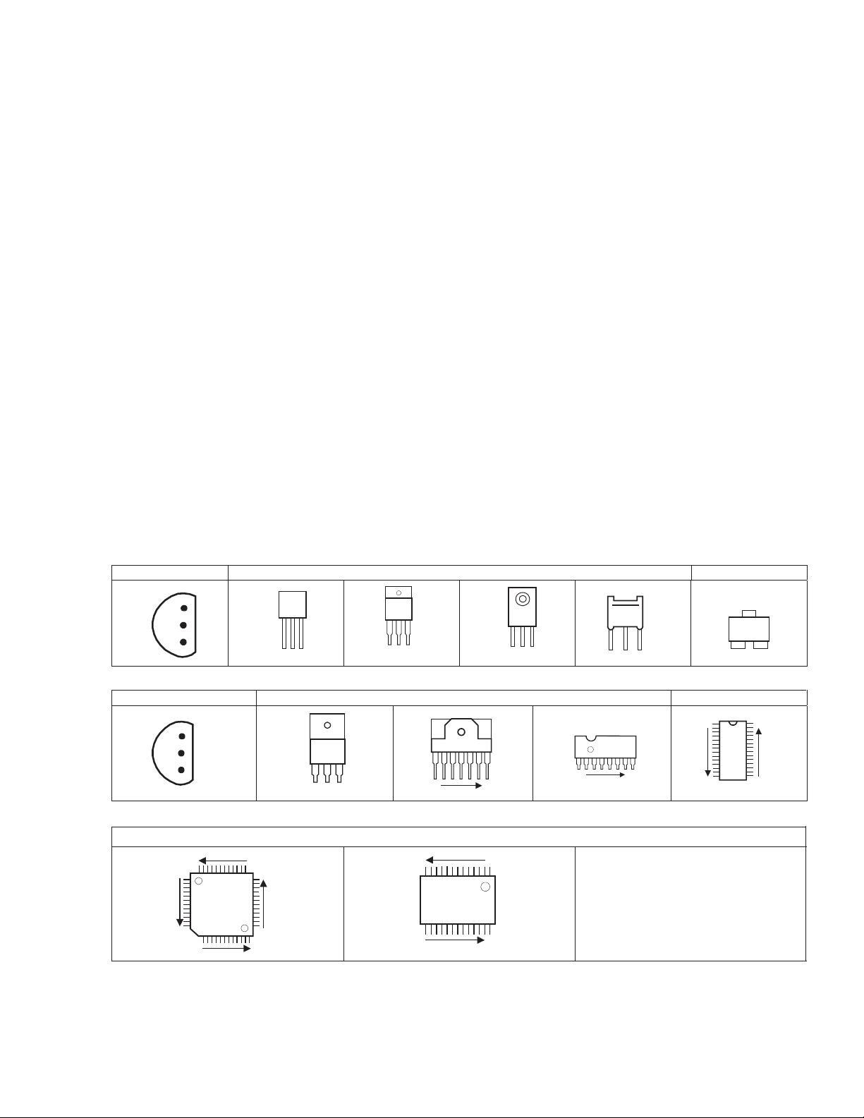
SEMICONDUCTOR SHAPES
TRANSISTOR
BOTTOM VIE W
E
C
B
ECB
BCE
(G)(D)(S)
FR ONT VI EW
ECB
ECB
IC
BOTTOM VIEW FRONT VIEW TOP VIEW
OUT
E
IN
IN OUTE
1 N
1 N
CHIP IC
TOP VIEW
N
N
1
TOP VIEW
CHIP TR
1
C
BE
N
N
1
N
No.52104
N
2-2
Page 4
A V-32430
S
L
P
N
C
C
A V-32432
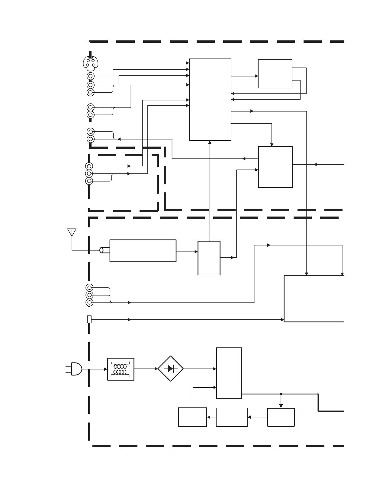
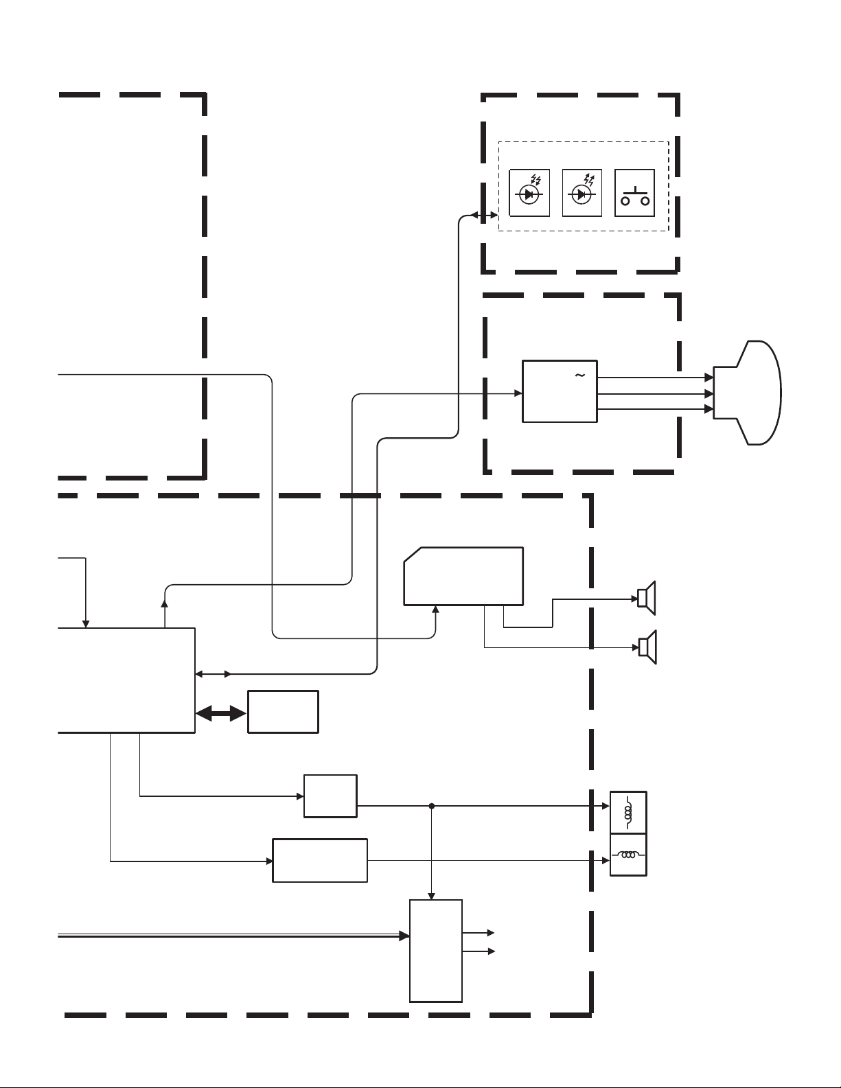
BLOCK DIAGRAM
INPUT 1
(S,V,L,R)
INPUT 2
(L,R)
AUDIO
OUT
INPUT 3
Y/C
V1
L1
R1
L2
R2
L
R
V3
L3
R3
TERMINAL
FRONT
PWB
Y/C
V1
L1/R1
L2/R2
V3
L3/R3
IC5501
AV SW
VTV
VTV
Y/C OUT
L/R OUT
MON L/R
Y
C
MPX
V
IC5201
3LINE
YC SEP
IC5001
MULTI
SOUND
PROCESS
&
AUDIO
CONTROL
Y
C
AV
INPUT 2
(Y,Pb,Pr)
AV
COMPULINK
TU001
TUNER
IF
IC101
MPX
Y/Pb/Pr
IF DET
Y/C OUT
Y
Pb
Pr
IC201
MICRO COM
CLOSED CAPTIO
VIDEO PRO
COMP LINK
DEF. PRO
MAIN PWB
T921
SW.
TRANSF.
LF901
D901
IC911
POWER IC
PC921
VOLTAGE
FEED BACK
IC921
ERROR
AMP
B1
2-3
No.52104
Page 5
V SELECTOR
PWB
A V-32430
A V-32432
FRONT CONTROL
PWB
RM LED SW
CRT SOCKET
PWB
L/R
b/Pr
201
COMPUTER/
PTION DECODER/
PROCESS./
PROCESS
V
H
R/G/B
IC702
MEMORY
L , R
L/R
IC621
AUDIO AMP
L R
R/G/B
Q3351
Q3353
RGB OUT
R
L
CRT
SP R
SP L
B1
Q511
H.OUT
IC421
VERT OUT
T502
HVT
No.52104
DY01
(ITC)
H
V
FOCUS
SCREEN
2-4
Page 6
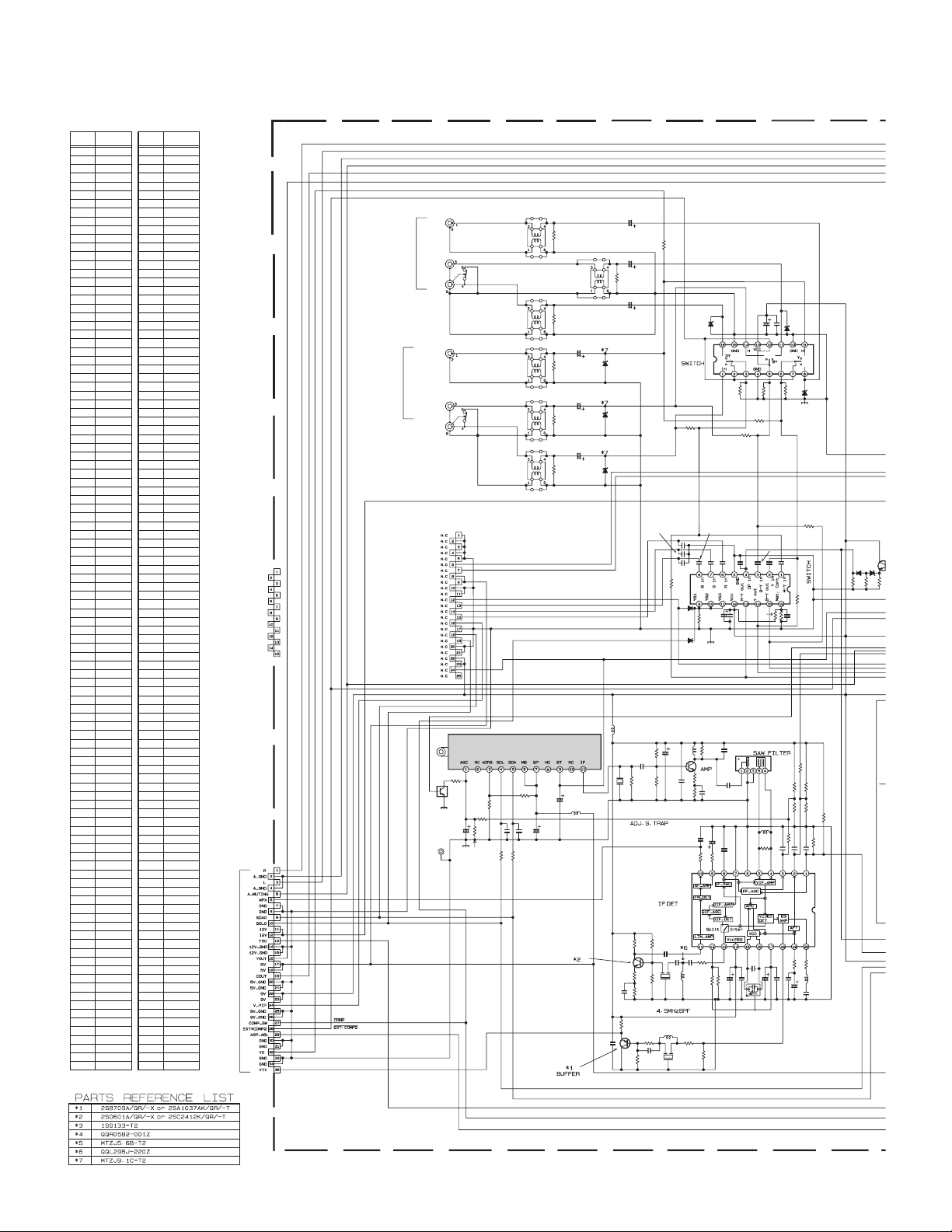
A V-32430
2
6
6
P
O
A V-32432
CIRCUIT DIAGRAMS
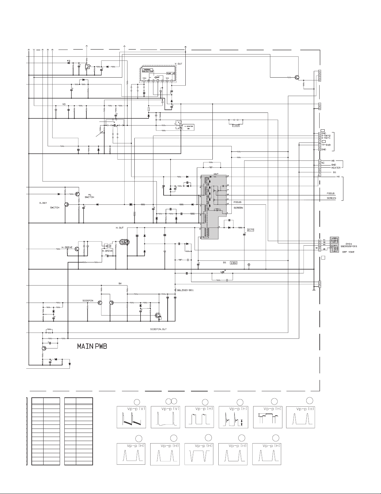
MAIN PWB CIRCUIT DIAGRAM (1/2) SHEET 1
VOLTAGE (V
)
28 0
IC601
1 6.1
2 6.1
3 6.1
4 0
5 0
6 6.1
7 6.1
8 6.1
9 0
10 0
11 0
12 9
13 4.8
14 0
15 4.8
16 2.9
IC621
1 1.2
2 1.3
3 0
4
5
6 11
7 22.2
8 22.3
9 1.8
10 0
11 10.6
12 0
13 10.6
IC702
1 0
2 0
3 0
4 0
5 4.7
6 4.8
7 0
8 5
IC703
1 5
2 5
3 0
IC704
1 5
2 11.5
3 0
IC852
1 13.6
2 9
3 0
IC853
1 9.4
2 4.8
3 0
TU001
1 1
2
3 4.7
4 3.9
5 4.2
6 4.7
7 4.7
8
9 31.3
10
11 0
Q101
E 1.8
C 9
B 1
Q131
E 1.6
C 0
B 0.9
Q161
E 5.8
C 2
B 2.6
Q211
E 3.8
C 9
B 4.5
Q232
E 0
C 0
B 0.5
Q233
E 3.4
C 9
B 4
Q701
E 3.6
C 2.4
B 3
Q352
E 5.4
C 9
B 6
Q623
E 0
C 13.7
B 0.1
PIN NO. PIN NO.
IC101
1 2.5
2 4.8
3 1.4
4 1.4
5 0
6 0
7 0
8 3.2
9 2.3
10 5.5
11 2. 1
12 3.3
13 2.1
14 9
15 3.9
16 3.9
17 4.8
18 2
19 3.4
20 1.5
IC201
1 2.8
2 2.1
3 4.7
4 0
5 5
6 2.2
7
8 0
9 5
10 0
11 0
12 0
13 1.1
14 1.9
15 9
16 6.6
17 3.4
18 4.1
19 3.2
20 0
21 0
22 2.1
23 2.2
24 2
25 5.1
26 2.1
27 2
28 2.3
29 0
30 2.1
31 5.9
32 0.1
33 2.5
34 3.8
35 1.6
36 2.5
37 2.8
38 4.7
39 1.8
40 1.9
41 1.9
42 9
43 0
44 0
45 0
46 5
47 0
48 0
49 4.6
50 4.6
51 4.7
52 2.5
53 4.8
54 0
55 4.9
56 0.4
IC501
1 2.3
2 2.3
3 0.8
4 4.9
5 9
6 2.2
7 4.8
8 0
9 11.5
10 0
11 3. 3
12 0.5
13 8.7
14 3.7
15 12
16 4.7
17 4.7
18 4
19 0.6
20 2.8
21 8
22 2.4
23 1.1
24 7.1
25 11.7
26 2.5
27 0
VOLTAGE (V
)
SELECTOR
(SHEET 3)
CN003
CN001
AV
PWB
INPUT 2
OPEN
QNN0349-002
Q001
UN2212-X
OPEN
NQR0169-001X
NQR0169-001X
NQR0169-001X
TUNER
0
C010 C011
OPEN OPEN
R003
100
Y607
C612
*
R613
*
*
R008
82
1k
R166
R169C165
560.01
1k
C657 C656
OPEN OPEN
R101
5.6k
.01
R102
1.8k
M52342SP
R165
22k
C166
.01
10k
CF161
QAX0642-001Z
QQL29BJ-150Z
R134
CH
C132
OPEN
QAX0639-001Z
4.5MHz TRAP
IC101
L131
CF131
0
C658
OPEN
100
R612
C006
C105
.01
2SC5083/L-P/-T
L161
15
IC602
OPEN
R653
D653
D654
OPEN
QQLZ014-R22
/25
47
R105
C162
OPEN
R162
22
47p
C164
R132
R131
0
OPEN
27
0
D606
OPEN
C604 C605 C606
OPEN OPEN OPEN
C607
OPEN
R655
OPEN
L101
.22
R103
100
R1/2
Q101
R104
18
C102
.01
C161
/50
R164
1k
47p
R171
10k
C163
330560
1k
R618 R617 R616
OPEN OPEN OPEN
C608 R615
OPEN
C103
OPEN
C104
.01
10
R161
3.3k
22k
R163
C106 C107
/25
47 .01
OPEN
Y609
C613
R605
OPEN
OPEN
Y610
C614
D601
/25
D602
/25
D603
/25
L113
4.7
QQL29BJ-4R7Z
C101
CF001 R112
QAX0349-001
R167
R168
100
R135
C131
.01
R133
820
R652
C651
OPEN
TF
.22
C116
QQR0907-001
0
T111
C615
OPEN
R651
QAX0723-001
L102
R114
C122
C616
OPEN
D605
OPEN
D604
OPEN
0
COM_Y
R611
100
C653C652
C654
OPENOPEN
OPEN
OPEN
IC601
R610
100
R614
OPEN
SF101
R117
27k
R118
22k
OPENOPEN OPEN
100
R113
C124
/25
C118
C117
.01
47
C119
C655
OPEN
OPEN
R115
100
R111
390K
330K
R120
OPEN
R121
OPEN
.01
.01
.01
C114
C113
R119
/50
OPEN
68
R116
L114
.47
OPEN
C121
C120
OPEN
680p
CH
D354
MTZJ5.1B-T2
Q2
OP
D651
D652
OPEN
OPEN
R
R608R609
OPENOPEN
R
O
C22
.
/16
.01
C287
C288
100
R004
Y608
Y611
Y602
Y603
Y604
Y605
Y606
R002
100
0
R604
OPEN
OPEN
OPEN
R606
OPEN
R601
75
OPEN
OPEN
R602
75
OPEN
OPEN
R603
75
OPEN
C003
/50
10 56
QQL29BJ-560Z
C004
1000
/16
Q131
LC605
OPEN
C601
47
C602
47
C603
47
L001
Q161
LC604
OPEN
LC606
OPEN
OPEN
Y612
Y601
OPEN
LC601
LC602
LC603
J602
J602
J601
J601
OPEN
CN002
TU001
QAU0305-001
R009
6.8K
R001
OPEN
GND
R005
C001
/50
4.7
CN0E4
R006
OPEN
2-5
No.52104
Page 7
A V-32430
9
MTZJ5
1B T2
A V-32432
Q131
E
SGE-1061A-M2 : AV-32432
SGE-1062A-M2 : AV-32432
SGE-1063A-M2 : AV-32432
MAIN PWB
IC621
LA4485
1.0
C622
NCF21CZ-105X
C636
1
/50
R623
6.8k
C637
R638
1
/50
C621 C623
.001 .001
R622
680 680
R637
OPEN
Y631
OPEN
C633
OPEN
C635
OPEN
Q211
C212
10p
CH
R215C211
R212
/16
2.7k
N
C213
OPEN
Q261
OPEN
D651
D652
OPEN
OPEN
R607
OPEN
R608
N
OPEN
R291
OPEN
C222
.1
/16
.01
C287
C288
.
100
CH
R213
OPEN
C214
OPEN
CH
R654
OPEN
R214
OPEN
R293
220k
560
470
R290
R288
R292
120k
.01
C237
100k
C221
.01
.01
10k
C241
C354
R359
R227
D353
Y201
0
R319
C302
C219
R219
5.6k10
OPEN
OPEN
CH
R220
R216
OPEN
Q212
5.6k
OPEN
0
R222
C218
OPEN
R218 R221
R217
1k
OPEN OPEN
CH
C609
R657
OPEN
.1
150k
.01
.22
C610
OPEN
R656
C203
R318
OPEN
/50
10
/50
C242
2.2
.47
C402
C281
C285
R289
10
/50
100
.1
100
R287
C611
C286
R281
IC201
TM8812CSANG3PF2
MICOM/V/C/DEF
.0015
/50
/16
.01
1
C202
C244
C243
100
OPEN
100
100
2.2
22k
R201
L241
22
R202
R304
R305
R301
D308
D305
D309
D306
D310
D307
R231
C223
1.8k
.01
Q213
OPEN
/16
3.9k
100
C282
R282
2.2k
R302
NCB31HK-103X
100
R303
2.2k
R306
1k
R728
L232
QQL29BJ-560Z
TV
R238
47k
C283
C284
680
OPEN
2.2/50
R283
R284
4.7k
R739
R286
.01
C392
L391
22
C712
/16
/16
C711
L704
22
C391
100
100
D700
R360
L705
4.7k
4.7k
100
100
100
R733
R734
R731
R732
R708
C233 C234
68p
CH
56
.01
/16
100
C704
0
.01
C705
.01
22k
R729
D701
22
6.8k
R769
R740
10k
R237
3.9k
OPEN
R241
3.3k
Q232
R243
1.5k
L701
22
L702
22
22p
C708
X701
QAX0717-001Z
4.7k
/50
1
C706
D704
D703
R704
C716
10
Q701
R827
1k
OPEN
R772
10k
D710
D709
D708
C625R621
1.0
1006.8k
/16
C624
0
0
NCF21CZ-105X
R639
R624
Q624
D621
OPEN
OPEN
R633
OPEN
Q623
UN2212-X
Q233
R816
120K
R706
4.7k
22p
1k
C709
D723
.01
C728
R702
1k
100
4.7k
R721
OPENOPEN
.001
C700
R717
R705
R709
R716
OPEN
/50
D716
OPEN
220
220
220
220
R768
R767
R766
R765
R764
1000
D622
OPEN
R821
R700
R812
CN00C
C626
R707
10k
R822
4.7k
180K
C815
0.01
R714
100
1k
R811
OPEN
R718
22k
D706D707
NOT USED
/25
47k
C813
R715
AU_VCC
C634
OPEN
R632
22k
R631
33k
R630
OPEN
IC703
S-80840CNY-T
Q700
OPEN
OPEN
10k
22k
R626
10
R754
OPEN
R737
OPEN
Q705
OPEN
R776
OPEN
C807
470
AT24C04W-32430
C703
IC702
C627
R701
10k
MEMORY
C630
OPEN
/50
/50
/MA
SGE-1064A-M2 : AV-32430
/YA
SGE-1065A-M2 : AV-32430
/RA
SGE-1066A-M2 : AV-32430
HS001
C629
1000
/25
D625
AN78L05-T
C702
/50
IC704
R629
OPEN
OPEN
D624
R628
OPEN
OPEN
C628
1000
/25
C701
10
/50
J810
OPEN
FRONT CONTROL
PWB
(SHEET 5)
D810
OPEN
22k
R627
/50
.47
A_MUTING
Q621
OPEN
Q622
D705
10
OPEN
D721
OPEN
R755
R756
OPEN
R775
C726
OPEN
OPEN
D722
OPEN
CN007
QGA2501C5-04Z
SPEAKER
R859
BW
D855
BW
V_OUT
H_OUT
FBP
EW
X_RAY
R358
OPEN
R353
OPEN
CEHT11B-002Q
R354
0
CN0SS
C854
220
R857
QRG029J-330
/16
HS006
QRG029J-180
D352
R352
10K
Q353
OPEN
/MA
1
/YA
/RA
18
IC101
2
OPEN
CN0L1
14
IC201
5
AU_VCC
AU_GND
IC201
18
1.4
IC201
28
12.0V
IC851
R856
OPEN
OPEN
C851C852
OPENOPEN
AN7809F
AN7805F
220470
Q352
9V_VC
IC852
C853
220
/16
R855
10
STB_VCC
IC853
C856C857
/16/16
5V
GND
V_OUT
H_OUT
FBP
EW
STB_5V
X_RAY
VP2
BT
ABL
OCP
EHT
MAIN_POW
SCL0
SDA0
33
2W
QRG039J-100
R858
18
2W
HS007
OPEN
C352
33
/16
R355
0
R356
12k
1
12V
IC201
39
3
IC201
40
3
41
IC201
3
QGA2501C5-05Z
CN004
CRT
SOCKET
PWB
(SHEET 4)
No.52104
2-6
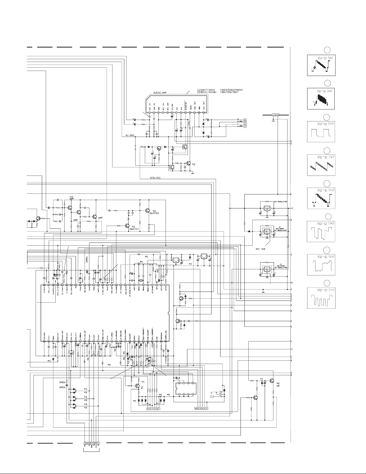
Page 8
A V-32430
O
A V-32432
MAIN PWB CIRCUIT DIAGRAM (2/2) SHEET 2
QGA7901C1-02
CNDEG
POWER
CORD
CN0PW
F901
QMF51N1-5R0-J5
QMF0007-5R0J1
VA901
ERZV10V621CS
C901
QFZ9072-104
QFZ9075-104
LF901
QQR0527-003
QQR1085-003
C902
QFZ9072-473
QFZ9075-473
LF902
OPEN
BW
BW
Y901
Y902
C903
OPEN
TH901
QAD0132-3R0
C909
OPEN
R902
OPEN
RGP10J-5025-T3
IC911
STR-G6624/F8
D918
MTZJ5.1C-T2
QCZ9054-102
100
D910
MA700A-T2
TH902
OPEN
C905
D911
R911
22k
1/2w
R901
R930
22k
QRF074K-R47
1/2w
K917
*4
K916
C914
/50
*4
K918
K912
D917
MTZJ30A-T2
R913
.22
C913
R912
.22
470p
1/2W
MY,5%
R914
680
D912
RGP10J-5025-T3
C920
OPEN
D914
*3
C917
.0018
D913
RGP10J-5025-T3
Y903
R917
3.3k
BW
QCZ9054-102
GSIB460-S1
QCZ9054-102
QCZ9054-102
QFP32GJ-103
QRG01GJ-470
QCZ0340-2222WMFR
2WMFR
BW
Y904
C906
D901
C908
C904
C907
/200
470
F905
QMFZ034-5R0Z-J1
C919
R909
47
D915
SARS01-T2
C912
2200p
R918
2.2K
1/2W
C916
330p
D920
*3
R915
1/2W
2KV
6.8
C918
.1
B2
R998
QRZ9041-275
C997
QCZ9052-102
K914
QCZ9074-103
R999
T951
QQT0372-001
QQT0355-001
RY951
QSK0085-001
QSK0086-001
QSK0130-001
Y918 Y919
OPEN BW
R919
680k
R1/2
K920
Y916
BW
Y917
BW
BW
T921
QQS0138-001
PC921
TLP421F/D4-GR/
QCZ9074-103
C998
C999
MAIN_POW
AU_GND
AU_VCC
MAIN_POW
Y914Y910
OPEN
AU_VCC
Y913
AU_GND
1000P
BW
QCB32HK-102Z
C937
D931
RU30A-F1
R581
C551
OPEN
STB_VCC
STB_VCC
RU3YX-LFC4
RU3YX-LFC4
OPEN
MTZJ9.1B-T2
C941
.001
D935
C939
QCB32HK-152Z
D933
2kV
C931
100
OPEN
R582
OPEN
R583
D945
1500P
/160
IC501
R589
OPEN
CN0E3
K935
*4
BW
K933
*4
Y912
OPEN
K932
Y909
*4
OPEN
K931
*4
R924
2.2k
1/2W
GND
GND
D957D954
1N4002G-T21N4002G-T2
D955
1N4002G-T2
R954
BW
C922
OPEN
OPEN
OPEN
OPEN
R586
OPEN
R585
R584
R590
OPEN
D956
1N4002G-T2
Q951
2SD1383K/AB/-X
R951
47k
CP936
ICP-N70-T
CP
CP932
ICP-N70-T
CP
C933
1000
/16
L940
OPEN
R587
C925
OPEN
IC921
SE135N
R591
OPEN
OPEN
R588
R594
OPEN
OPEN
OPEN
Q551
OPEN
C553
C552
BT
BT
D953
*3
R953
82
1/2W
GND
Q552
OPEN
12V
12V
C951
470
/16
R950
0
C935
1000
/25
C934
150p
L933
47
QQL26AK-470Z
L931
47
QQL26AK-470Z
12.0V 5V
R595
OPEN
R592
OPEN
R593
OPEN
STB_VCC
R940
1/2W
180
D952
*3
MAIN_POW
C952
/16
220
R952
1k
C950
OPEN
Y905
OPEN
AU_VCC
R939
2.2
3W
AU_GND
12V
C938
470
/16
GND
R941
BT
18
2WMFR
D941
MTZJ33A-T2
K936
OPEN
OPEN
OPEN
C561
C562
R558
OPEN
R510
R559
OPEN
GND
OPEN
OPEN
SCL0
SDA0
R542
R507
OPEN
OPEN
OPEN
OPEN
R508
R506
R515
R509
IC502
OPEN
R514
OCP
H_OUT
EW
GND
9V_VC
V_OUT
H_OUT
EW
V_OUT
GND
C973
10
/50
C942
1
/50
OPEN
R540
R541
R972
OPEN
C971
100
/16
R975
22k
1/2W
R977
47k
1/2W
2-7
CN0SN
OPEN
No.52104
PIN NO.
VOLTAGE (V
IC421
1 0
2 15.2
3 30.3
4 2.6
5 2.6
6 29.3
7 3.3
IC501
1 2.3
2 2.3
3 0.8
4 4.9
5 9
6 2.2
)
PIN NO. PIN N
VOLTAGE (V
7 4.8
8 0
9 11.5
10 0
11 3 .3
12 0.5
13 8.7
14 3.7
15 12
16 4.7
17 4.7
18 4
19 0.6
20 2.8
21 8
)
22
23
24
25
26
27
28
IC911
1
2
3
4
5
IC921
1
Page 9
A V-32430
A V-32432
R446
OPEN
R423
39k
Y412
OPEN
Y414
OPEN
Y413 Y415
BW BW
R523
33k.82
MA4068N/Z1/-T2
NRVA02D-222X
Q511
2SD2634-YD
R511
1/2W
X_RAY
HS003
IC421
V_NECK
R430
0
BW
BW47BW
Y401
Y402
Y405
R424
39k
R441
0
C427
1
/50
Y411
OPEN
22
R544
3.9K1.2K
1/2W
R548
1.5K
1/2W
C430
OPEN
K401
QQR0621-002Z
MY
D422
MTZJ75-T2
C431
.056
100V
R537
NRVA02D-752X
D531
R535
C525
100
/25
MTZJ5.1C-T2
C510
D501
*
RH3G-F1
D502
R545
*
R550
R549
OPEN
OPEN
R551
D542
OPEN
OPEN
C542 R552
OPEN OPEN
2SD1408/OY/-LB
VP2
LA7841
VP2
C424
10p
100
/35
C422
C440
.01
D529
Q543
/MA
/YA
/RA
D421
C524
OPEN
1SR35-400A-T2
R529
330
R522
OPEN
C514
.18
QFP32GJ-183
R553
C508
4.7
/50
R434
180
2WOMR
R435
1k
R453
OPEN
1N4003-T2
C425
4702.7k.018
/35
1/2W
R555
3.3
2W
RGP10J-5025-T3
C523
QEHR1VM-108Z
D537
FR525
4.7
QRZ9017-4R7
C528
OPEN
C527
.01
R526
2.7k
1/2W
D526
1SS81-T5
C513
13000p
/1400
N
C505
OPEN
L513
OPEN
PP
/400
*
QQLZ027-821
N
N
4.7
S421
D524R556
OPENOPEN
D523
FR527
QRZ9011-470
D507
OPEN
R513
OPENRU3AM-LFC4
C517
OPEN
C515
L512
C507
1/2W
1SS81-T5
*
/50
C531
.001
D525
QSL4A13-C02
47
Vcc
VDY
C504
100
SGE-1064A-M2 : AV-32430
SGE-1065A-M2 : AV-32430
SGE-1066A-M2 : AV-32430
Q451
R451
OPEN
OPEN
R452
OPEN
Y404
BW
CN00A
R527
1/2W
150k
R528
1/2W
R557
OPEN
L521
T502
/160
680
150k
*
C522
OPEN
R554
FR
D521
RH1S-T3
L511
R512
1/2W
C516
560p
QRK126J-150X
C521
10
/250
CN0E1
/500
OPEN
CN00K
OPEN
CN009
QJB003-033626
CN0S1
S1
FOR TEST
B1
CN0B1
CN005
QGA2501C5-06Z
CRT SOCKET
(SHEET 4)
CNDAF
CRT SOCKET
(SHEET 4)
CN0HV
CHC802T-05N-J
HV
GND
OPEN
CN008
WJM0212-003A
/MA
/YA
/RA
R431
1.5k
C433
47
/25
R421
8.2k
R429C435
C526
R533
12k
R534
12k
R538 C533
33k 10
D973
*3
STB_5V
R449
Q431
UN2212-X
10k
R432
TF
C502
330p
R503
10k
R505
QRL039J-102
/25
C432
100
QETM1EM-228
1SR124-400A-T2
1/2W
D431
R447
OPEN
100k
C429
R448
OPEN
47k
D423
OPEN
R433
680
R426
R422
18k
OPEN
C428
2200
/25
R428
OPEN
R427
1.0
/2W
D527
R524
56K
QRJ146J-333X
FBP
Q532
BW
D534
/50
T501
CE42034-002
/500
C503
QEHR2CM-105Z
C501
.01
R504
3WMFR
3WMFR
QRL039J-102
R543
1/2W
Q541 Q542
R547
*1 *1
100K
SGE-1061A-M2 : AV-32432
SGE-1062A-M2 : AV-32432
EHT
FBP
GND
ABL
V_OUT
D432
R450
OPEN
ABL
V_OUT
C403
OPEN
CH
GND
2SC2785/JH/-T
R572
OPEN
R573
OPEN
QRT029J-1R2
QRT029J-1R2
R972
OPEN
C971
100
/16
R975
2SA1208/ST/Z1-T
22k
1/2W
MTZJ15C-T2
R977
47k
1/2W
B2
VGND
R531
QRJ146J-391X
ABL
R532
27K
D535
*3
Q531
Q501
2SC4212/Z1/
R502
R501
0
270
R546
330
R570R571
OPENOPEN
D543
OPEN
C543
OPEN
R979
R980
R973
2.7k
1/2W
Q971
D972
R978
C972
33k
47
/25
SGE-1063A-M2 : AV-32432
PIN NO.
VOLTAGE (V
22 2.4
23 1.1
24 7.1
25 11.7
26 2.5
27 0
28 0
IC911
1 152.2
2 0
3 288
4 17.8
5 1.5
IC921
1 135.2
)
PIN NO.
2 11.5
3 0
PC921
1 12.5
2 11.5
3 1.5
4 16.1
Q501
E 0
C 75.1
B 0.3
Q511
E 0
C 130
B -0.1
VOLTAGE (V
)
IC421 5
60
T502
85
IC421 3 7
30
4
2
T502
35
0.9
250
Q501 B
T502
6
140
0.9
Q501 C
T502
78
80
Q511 B
2
T502
1100
No.52104
Q511
C
2-8
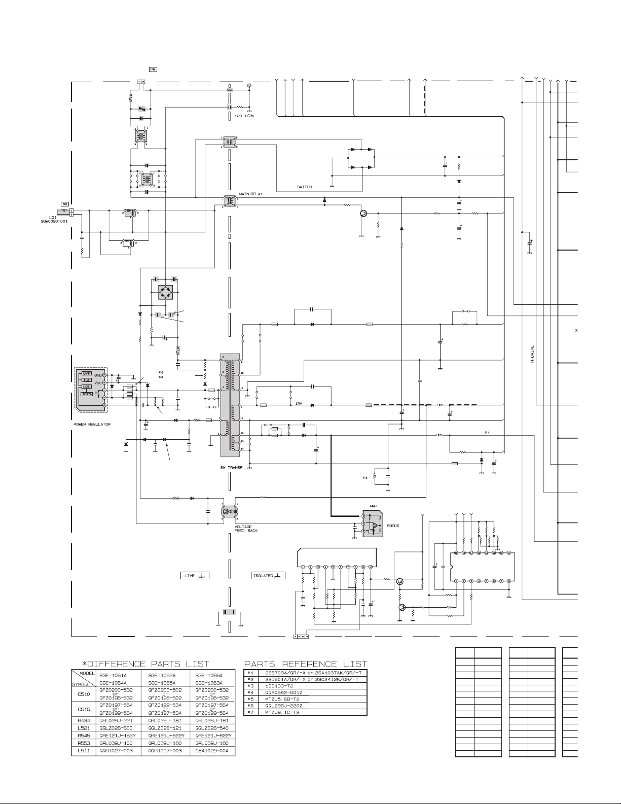
Page 10
A V-32430
0
A V-32432
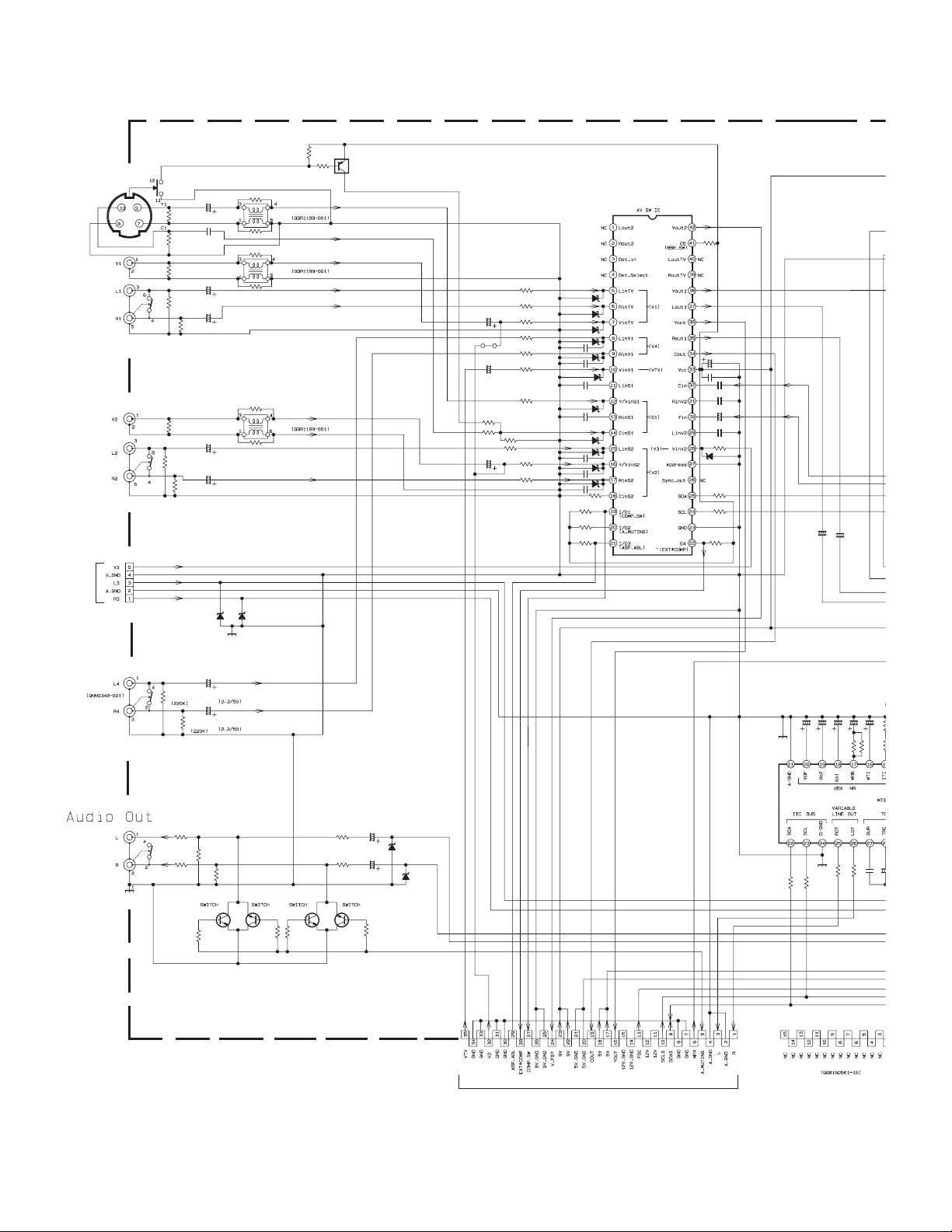
A V SELECTOR PWB CIRCUIT DIAGRAM SHEET 3
R5524
10k
R5526
10k
Q5501
0
0
LC5501
C1
LC5502
LC5503
Y1
OPEN
V1
OPEN
OPEN
DTA114TSA-T
INPUT 1
QNZ0454-001
INPUT 3
FRONT
TERMINAL
PWB
(SHEET 6)
J5501
J5502
QNN0348-001
CN5006
QGA2501C5-05Z
R5521
R5558
C5508
R5519
/50
10
75
R5520
C5509
75
.01
75
R5522
C5501
220k
R5523
C5502
220k
R5527
75
C5520
2.2/50
LV2
R5532
220k
C5521
2.2/50
RV2
R5533
220k
D5011
*7
0
R5559
0
R5560
0
R5561
0
/50
2.2
/50
2.2
R5564
R5565
D5012
*7
Y5501
R5507
R5509
C5506
C5503
10/50
OPEN
220
OPEN
C5504
N
IC5501
TA1218AN
R5517
10k
R5501
220
D5501
15k
220
D5514
C5537
D5515
C5538
D5508
OPEN
D5509
OPEN
D5510
OPEN
OPEN
OPEN
OPEN
OPEN
D5502
D5503
D5504
D5505
D5507
C5541
OPEN
C5542
OPEN
C5543
OPEN
R5513
*7
*7
R5514
10k
R5515
10k
R5516
10k
*7
C5532
/25
*7
C5539
OPEN
*7
C5540
OPEN
*7
15k
C5533
C5535
C5534
C5536
R5543
R5544
R5545
R5546
10k
C5531
D5513
47
.01
.01
OPEN
/16
10
N
OPEN
220
*7
330
330
C5027
C5028
/50
1
/50
1
N
N
R5502
220
R5503
220
OPEN
R5568
OPEN
R5569
/16
10
R5504
220
R5505
220
10k
R5508
R5510
220
R5511
220
R5512
J5504
OPEN
J5503
QNN0348-001
R5566
OPEN
R5396
R5395
C5544
OPEN
C5545
R5567
OPEN
OPEN
C5391
R5391
/50
.47
220
R5393
82k
R5394
220
82k
Q5387
R5387
22k
R5386
DTC323TK-XDTC323TK-X DTC323TK-XDTC323TK-X
22k
Q5385Q5386 Q5384
R5385
220
R5392
220
22k
R5384
D5391
*7
C5392
/50
.47
22k
D5392
*7
CN5001
QGB1505K1-35
MAIN PWB
(SHEET 1)
R5011
/50
C5018
1331
100 100
R5012
C5017
/50
/50
C5016
CN5003
OPEN
R5010
R5019
C5015
1
5.6K
100
/50
IC5001
R5020
C5019
100
56K
R5009
.022
R50
C5014
R5008
1.
/50
10
C5020
15K
/50
2.2
2-9
No.52104
Page 11
A V-32430
R5009
022
56K
A V-32432
VOLTAGE (V
)
34 3.7
35 3.9
36 3.7
37 3.9
38 4.4
39
40
41 0.1
42 4.4
IC5151
1 4.5
2 4.5
3 4.5
4 4.5
5 4.5
6 4.5
7 4.5
8 9
9 9
10 0.1
11 0
12 9
13 4.5
14 4.5
15 4.4
16 4.5
17 4.5
18 4.5
19 4.5
20 4.5
IC5201
1 4.8
2 1.3
3 3
4 2.3
5 1.4
6 4.8
7 0
8 4.8
9 4.2
10 3.6
11 0
12 0
13 2.4
14 1.6
15 4.8
16 0
17 2.3
18 3
19 1.7
20 2.3
Q5211
E 6
C 9
B 6.7
Q5212
E 5.4
C 9
B 6
Q5251
E 2.3
C 8.4
B 2.9
Q5252
E 9
C 3.7
B 8.4
Q5253
E 2.9
C 0
B 2.3
Q5261
E 2.9
C 0
B 2.3
Q5262
E 2.3
C 8.4
B 2.9
Q5263
E 9
C 3.7
B 8.4
PIN NO. PIN NO.
IC5001
1 4.1
2 4.1
3 4.1
4 4.1
L5251
L5201
.01 47
C5213
R5215
*2
1.5k
L5211
4.7
180
QQL29BJ-4R7Z
Q5218
OPEN
R5231
OPEN
R5233
Y5202
0
R5003
4.7K
/50
C5009
.47
BW
C5204 C5203
.01 47
47p
C5214
180p
R5216
1.8k
C5245
OPEN
R5235R5232R5229
OPENOPENOPEN
R5234
OPEN
OPEN
R5002
15K
C5007
2.2
C5008
.047
1K
R5001
R5014
100
Q5212
*2
L5246
OPEN
QQL29BJ-4R7Z
Q5219
OPEN
/50
N
N
R5013
100
/25
QQL29BJ-4R7Z
L5242
BW
C5244
OPEN
L5243
4.7
/50
C5004
C5006C5005
4.71
0.1
/50
100
R5017
R5018
L5241
100
IC5201
C5233
0.01
C5234
0.01
0.01
C5001
/16
C5215
C5235
.01
C5237
0.01
C5239
R5243
100
R5242
100
C5002
C5026
TC90A49P
C5232
0.01
C5240
0.01
C5241
OPEN
0.01
C5243
0.01
QQL29BJ-4R7Z
R5241
820
C5226C5223
.01
R5236
OPEN
C5242
100
C5246
.47
/50
0.01
L5245
Y5201
0
/16
100
1
/50
C5231
100
4.7
C5236
100
/16
C5238
100
/16
/25
C5003
47
R5016
100
100
R5015
R5210
0
EF5201
OPEN
C5208 C5206C5209 C5205
OPENOPEN /25
R5211
3.3k
C5211
R5217
2.2k
33K
R5005
0.1
C5011
0.1
C5012
C5023
/50
3.3
/50
2.2
R5213R5212
1k10k
OPEN
R5021 R5004
3.3M 68K
0.1
C5010
UPC1851BCU
C5024
.0022
Q5211
R5214
C5212
R5230
OPEN
C5025
100p
0.1
10
/16
N
R5007
C5013
1
1.5K
/50
/50
C5014
10
3.3K
R5006
15K
R5008
01
/50
2.2
C5022
C5020
.
C5021
.0022
BW
C5251
47
/25 OPEN
R5258
100
/16
L5244
4.7
180p
C5247
0.01
C5248
OPEN
R5240
0
R5261
100
SGE-5061A-M2 : AV-32432
SGE-5062A-M2 : AV-32430
C5252
.01
Q5253
R5262
2.2k
Q5261
0.9
R5259
2.2k
R5251
470
C5253
82P
R5263
470
OPEN
QQL29BJ-150Z
IC5201 4
C5254
R5252
C5262
OPEN
R5264
L5261
OPEN
L5202
OPEN
15
Q5251
*2
15
C5255
47P
QQL29BJ-150Z
R5269
680
Q5262
*2
C5263C5261
15p
Q5252R5255
*1680
R5254
1k
R5253
1k
Q5263
*1
R5270
1k
R5265
1k
IC5501 10
0.8
/MA,
AV-32432
/MA,
AV-32430
/RA,
/RA,
AV-32432
AV-32430
5 4.1
6 3.8
7 0
8 4.1
9 3.9
10 4.1
11 4
12 4.5
13 4.1
14 1.2
15 1.2
16
17 0
18 3
19 9
20
21 4.1
22 4
23 4.7
24 3.8
25 4.1
26 4
27 4
28 2
29 4
30 4
31 2
32 4
33 4
34 4
35 0
36 4
37 4
38 4.1
39 4
40 4.1
41 4.1
42 0
43 4
44 4.1
45 4.1
46 0
47 4.1
48 4
IC5501
1
2
3
4
5 5.2
6 5.2
7 5.2
8 5.2
9 5.2
10 5.1
11 5.2
12 5.1
13 5.2
14 1.7
15 5.2
16 5.2
17 5.2
18 1.7
19 4.2
20 3.3
21 0.1
22 7.5
23 0
24 3.7
25 4.2
26
27 0
28 5.2
29 5.2
30 5.1
31 5.2
32 5.1
33 9
/YA
/YA
VOLTAGE (V
)
AV SELECTOR PWB
No.52104
2-10
Page 12
A V-32430
3
0
A V-32432
CRT SOCKET PWB CIRCUIT DIAGRAM SHEET 4
MAIN PWB
(SHEET 1)
CN3004
QJB003-054610
100 110
1k
1k
R3393
R3394
*3 1k
*3
*3
D3395 R3395
D3394
D3393
100
220
R3372
220
R3373
D3389
MTZJ5.1A-T2
D3390
R3374
220
C3357
100
/16
Q3353 CQ3352 CQ3351 C
Y3003
OPEN
R3365
10k
OMR2
R3368
2.2K
C3361
OPEN
R3364
OMR2
R3367
2.2K
C3362
R3366
2.2K
C3363
OPEN
Q3353
2SC4075/DE/YA11
R3356 R3359
10K
Q3352
2SC4075/DE/YA11
R3355
180
OPEN
R3363
10k
OMR2
180 100
R3362
1.5k
R1/2
QRZ0111-152
C3356
390p
5%
R3361
1.5k
R1/2
QRZ0111-152
C3355
330p
5%
R3358
100
R3360
1.5k
R1/2
QRZ0111-152
Q3351
2SC4075/DE/YA11
C3354
330p
5%
R3354
180
R3357
100
C3381
OPEN
R3381
390k
R1/2
QNZ0464-
SK3
Y3002
L3381
100
QQL29BJ-101Z
TP
2-11
R3391
1.5k
2SA933AS/QR/-T
Q3391
D3391
*3
3.9k
R3392
No.52104
C3391
220
/10
Y3001
C3392
100p
OPEN
5%
MAIN PWB
(SHEET 2)
CN3005
WJA0027-003A
Page 13
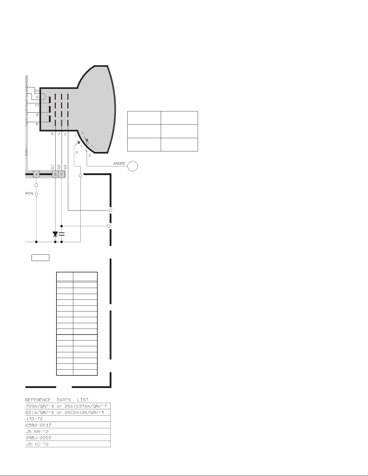
CRT SOCKET PWB ASS'Y
A V-32430
A V-32432
0464-001
SK3351
3002
SGE-3061A-M2 : AV-32432
AV-32430
SGE-3062A-M2 : AV-32432
B
R
G
CN30E2
V01
PICTURE TUBE
AV-32430/MA
AV-32432/MA
AV-32430/RA
AV-32432/RA
AV-32430/YA
AV-32432/YA
FOCUS
SCREEN
CN30SC
M80JUA061X06
A80AEJ15X01
A80AKB50X04
/MA,
AV-32432
/MA,
AV-32430
/YA,
AV-32430
/RA
/RA
/YA
-101Z
03A
TP-E
C3382
D3381
QCZ0121-102
BW
PIN NO.
Q3353
E 1.4
C 159.2
B 1.9
Q3352
E 1.5
C 157.3
B 1.9
Q3351
E 1.4
C 163.1
B 1.8
Q3391
E 8.4
C 1.9
B 9
VOLTAGE (V
)
No.52104
2-12
Page 14
A V-32430
7
7
P
W
7
A V-32432
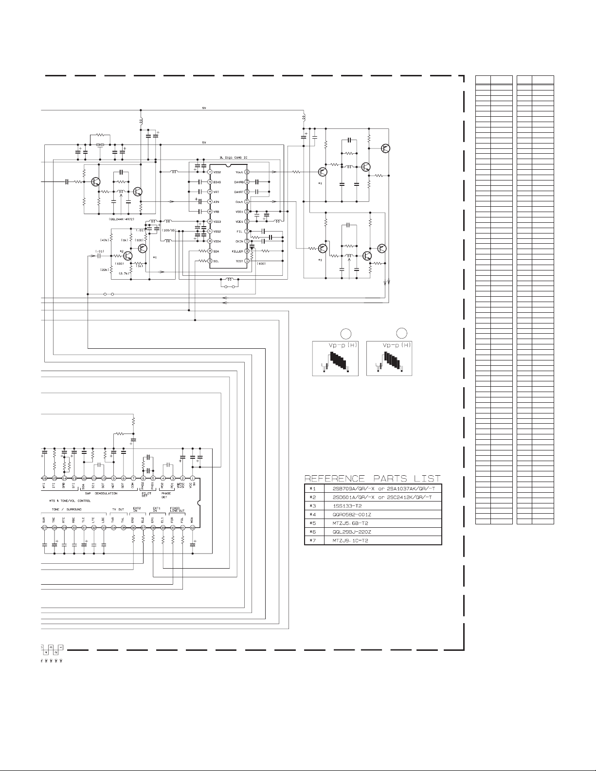
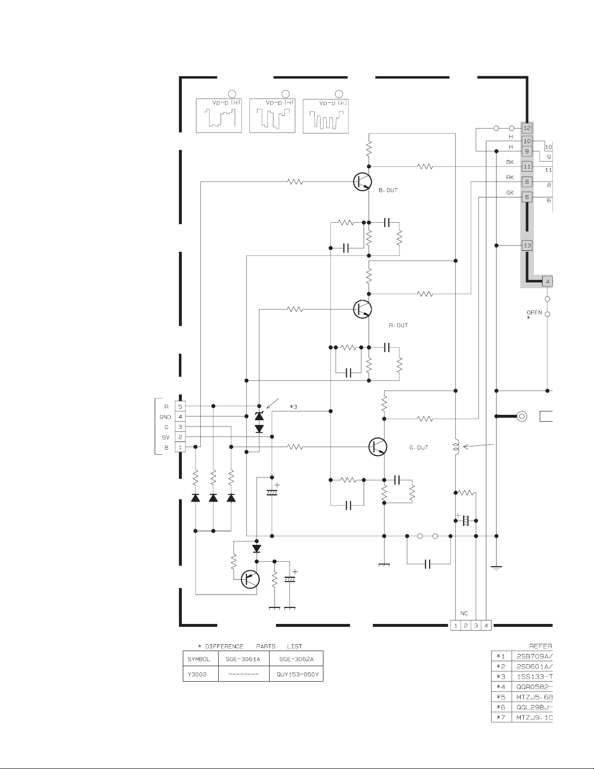
FRONT CONTROL PWB CIRCUIT DIAGRAM SHEET 5
CN7007
MAIN PWB
(SHEET 1)
REMOCON
KEY
P_LED
STB5V
GND
C7701
47
/25
IC7701
GP1UM281QK
R7711
100
R7709
560
R7710
100
D7701
GL2EG6
R7708
1.5k
Q7702
UN2112-X
S7
QS
R
O
SGE-
2-13
No.52104
Page 15
A V-32430
A V-32432
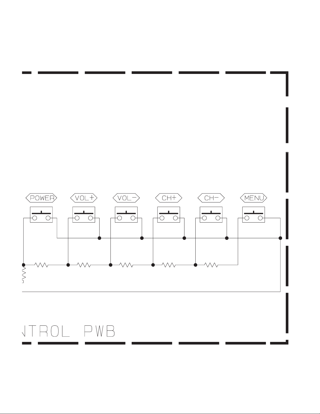
S7701 S7706 S7705 S7704 S7703 S7702
QSW0707-001Z QSW0707-001Z QSW0707-001Z QSW0707-001Z QSW0707-001Z QSW0707-001Z
R7706R7705R7704R7703R7702
5.6k2.7k1.5k1k1k
R7701
OPEN
-7061A-M2
No.52104
2-14
Page 16

A V-32430
A V-32432
FRONT TERMINAL PWB CIRCUIT DIAGRAM SHEET 6
CN6006
SELECTOR
AV
PWB
(SHEET 3)
V3
V3_GND
L3
A_GND
R3
QJB003-055620
OPEN
0
K6401
Y6001
C6401
2.2
C6403
2.2
/50
10
C6402
/50
/50
2-15
SGE-6061A-M2
No.52104
Page 17

Y6401
OPEN
A V-32430
A V-32432
1
0
02
3
R6401
75
R6402
220k
R6403
220k
LC6401
QQR1199-001
Y6402
J6401
QNN0417-001
INPUT3
OPEN
No.52104
2-16
Page 18

A V-32430
R538
Y
9
C403
W424
Q
W
A V-32432
PATTERN DIAGRAMS MAIN PWB PATTERN
W28
R623
R638
R639
R624
R621
HS001
W261
C624
Y612
D606
Y606
D603
Y604
D602
CN001
W27
W26
W24
CN003
C637
C623
TU001
D810
Y611
W252
R606
Y605
J810
W256
Y610
R603
W253
Y603
W492
R602
W491
W259
W497
W257
W258
W496
W490
W495
W494
W487
W486
W489
W488
R816 W431
R714
R822
R702
W485
W661
R739
C402
R429
C435
R283
R286
R281
R360
R302
R303
C392
C712
W29
W16
W480
W479
W478
W481
W483
W484
W23
W22
W255
W254
W659
C701
C621
C625
C626
R627
Q621
C627
Q622
R632
C630
R630
R631
D625
C629
W482
LC605
CN002
C815
R821
W251
R287
C244
R202
R301
C203
IC704
W250
C634
D624
C615
R653
R318
D622
R618
W249
R227
Q623
C628
Q261
Q624
R629
C606
C605
C656
C657
C633
Y609
R605
R651
R617
R637
W657
C635
R607
R654
W476
W658
W644
W643
W654
W653
W652
W651
W650
W649
W648
W647
W646
W645
W656
W655
W469
C702
D621
R715
W475
R812
W467
R628
C613
W474
W477
C604
W247
W244
W471
W21
R706
R721
W472
C658
W473
W246
W248
W468
W470
R655
C703
D723
W466
W463
Y631
R633
W462
R652
W465
R701
R716
W642
R855
R595
Y608
D605
W464
C608
D653
W461
R705
R709
J602
D651
L701
D705
R718
R708
W243
Q551
W241
LC604
C616
R608
C651
R609
IC601
W245
W641
R515
Q552
R593
D716
W242
W20
C856
R591
C652
R614
R707
C813
R811
R558
R592
Y607
D652
R704
CN007 SS
W19
Y602
R509
R594
W460
IC703
R731
IC702
W640
C561
W239
R559
R510
R604
IC201
R508
C562
W237
IC602
W459
C653
C704
W236
IC853
R858
R507
W240
D601
D654
C728
D703 D704
C601
D604
C612
R613
Y201
C709
C700
R700
W453
HS008
R542
R540
R514
W235
W238
C655
X701
R732
R506
R541
R589
W457
C654
R611
R615
R733
W454
C857
W232
Y601
LC601
R169
C165
R165
W234
L702
C807
IC502
R584
R601
R168
Q161
L113
C705
W456
R583
R167
C607
W233
R610
C708
W449
W230
L704
W458
J601
C162
R734
R582
W17
W452
W231
W262
C716
W660
W455
C106
R616
C282
R728
W450
CF161
IC501
L1
R612
C283
R585
W447
C164
R166
C166
W229
W227
R282
C706
D701
R772
W639
C853
IC852
C553
W228
R657
L705
HS007
R587
R586
R581
R162
W15
R656
R827
Q701
W638
R857
R588
R590
L161
C161
C285
C281
D700
C163
R163
R288
C284
R171
R161
R290
C854
W226
C551
R164
Q131
C107
C116
R291
C286
R289
C391
C711
R769
R740
W446
C552
SN
W225
R292
C131
L102
C288
C611
W445
C122
R135
T111
R114
SF101
R243
C237
R293
W637
C243
L241
R306
W632
W631
W444
D855
R133
C124
IC101
C610
W224
W223
C118
C132
C117
W13
W636
W14
L391
R134
C114
R218
R217
R221
W635
C609
C851
IC851
R131
R116
W222
R112
R222
C202
R305
W443
HS006
R859
CF131
W634
C222
D308
L131
R120
R121
C104
C241
D952
R119
W12
R201
C302
W221
D309
C951
C113
W633
W220
R304
D310
C852
L114
C121
R111
R103
C354
C120
R132
C119
W11
C102
Q211
Q212
Q213
R220
C234
D354
L232
R359
R319
C221
C242
R353
Q353
CN004
W630
R940
R115
C218
R118
R113
R117
L101
W442
C103
C287
R352
D305
R856
Q101
R237
D306
W629
R105
R104
D353
Q352
R358
W219
D307
W440
R005
R002
R101
Q233
W260
W25
C622
W493
R284
R717
C636
R622
IC621
R626
LC606
C614
LC603
C603
LC602
C602
W18
R729
R215
W441
R356
W218
R102
C006
C233
D956
R212
W628
R354
W437
T951
R008
R241
R355
W439
C105
C212
R231
R238
C352
D957
R006
C101
C952
R001
W438
W9
D352
W10
D954
D955
C010
W627
C011
W7
R216
R531
Q232
W434
W433
R009
R754
C211
W626
W625
W217
R003
R004
W6
W8
E3
L001
C003
W436
W435
CF001
W215
W214
W216
C223
C001
C004
R737
W623
R999
W622
W621
W619
W213
W212
W430
W429
W428
C997
E4
W618
W617
W620
R219
C219
W427
Q001
W616
W5
W432
W624
R213
C213
R768
R756
R214
C214
D709
Q700
W211
R998
C903
R767
R776
D721
R766
W426
R765
C433
D432
C533
W425
R764
D710
W20
R449
W423
VA901
D534
Y904
2-17
No.52104
Page 19

R767
R776
D721
4
211
R766
W426
R765
C433
D432
C533
R764
D710
W423
W209
R449
D534
Q705
C403
R421
W4
Y401
R755
W422
R543
R546
R571
W615
R538
CN009
W424
W613
W208
C440
HS005
Q531
D722
Y402
R544
R533
W421
Y405
W210
C430
D543
D706
W420
W611
IC421
R570
D708
D707
R534
R422
C726
R431
Q541
R572
Q532
D535
W614
R775
Y413
R532
C
W610
W612
R423
Q431
D423
R547
R573
W207
C422
R548
Q542
Q543
Q451
D531
C424
D421
HS003
R450
W206
W419
R451
R452
C543
C508
S421
R446
R549
R545
R427
C432
R448
D431
R433
R432
D542
R441
R550
R447
W418
R551
C507
S1
R428
C427
L512
R426
C542
R435
R424
W415
R552
R553
K
W416
C429
R430
R522
R526
R535 R537
E1
K401
D537
D529
C528
Y414
D422
CN008
C425
C428
C431
L513
W413
C524
Y412
C525
C517
Y415
R529
W414
Y411
R434
CN005
C521
FR525
W3
C523
D526
R453
Y404
C516
R512
R513
D507
W2
R556
A
C515
D527
A V-32430
A V-32432
D501
C
5
R528
R527
CP
W408
W407
W204
C513
D521
W203
HS004
C510
Q511
T502
T502
W405
R511
T501
C504
W402
DAF
W401
B1
R505
FRONT
R554
C522
R523
C526
R524
D525
W1
R557
L521
D523
D524
R
5
5
5
C527
C531
7
52
R
F
HV
L511
D
5
C505
0
2
1
4
W425
VA901
Y904
PW
C901
LF902
C902
Y903
Y902
FC901
F901
FC902
LF901
Y901
C950
R951
Q951
RY951
W609
R954
C904
W608
D945
W607
R952
R950
C
W417
W606
W605
9
0
W205
R501
D953
C938
L933
C909
TH901
R953
C934
W603
Y905
C933
R902
W604
TH902
R939
D933
L940
W409
CP932
C925
C939
C935
K936
C942
D941
CP936
Y914
Y910
C
9
9
8
C
999
DEG
F905
W411
W410
C906
D901
5
R901
C908
C907
K933
C919
R919
R909
R941
D935
C941
W602
R502
D915
Y918
C912
Q501
C973
K935
Y909
Y919
Y917
IC911
K920
K917
C502
R503
C931
Y916
K916
K931
K914
Y913
K932
C501
R915
R914
W202
C503
Y912
R978
C913
D931
C916
C920
R918
D912
T921
C937
C972
L931
D972
R504
D913
R917
IC921
D973
D914
C922
R977
C917
K918
R979
Q971
D918
R924
1
3
R973
R980
R972
C971
R975
W201
PC921
C918
W601
D920
R
9
R912
K912
D911
R911
R930
No.52104
C914
D917
W406
HS002
W404
W403
D910
2-18
Page 20

A V-32430
A V-32432
CRT SOCKET PWB P A TTERN
C3357
W3204
CN3004
W3401
R3366
C3363
C3354
R3354
R3357
Q3351
R3393
R3395
W3202
W3205
D3393
D3395
D3394
CN30SC
R3374
R3360
R3363
Q3391
R3394
C3391
C3382
R3392
R3391
R3361
D3381
D3391
Y3002
TP-E
W3402
Y3001
C3355
D3389
D3390
C3392
R3358
R3355
CN30E2
W3001
Q3352
R3362
SK3351
CN3005
C3381
Y3003
R3364
L3381
C3362
R3373
R3372
R3365
C3361
R3368
R3359 R3367
C3356
R3356
R3381
Q3353
TOP
FRONT CONTROL PWB P A TTERN
S7702
2-19
R7706
S7703
S7704
R7705
FRONT
S7705
R7704
R7702
R7708
R7703
S7706
R7701
CN7007
No.52104
W7401
S7701
Q7702
D7701
IC7701
R7709
R7710
R7711
C7701
Page 21

FRONT TERMINAL PWB P ATTERN
A V SELECTOR PWB PATTERN
R5264
R5269
L5261
R5262
R5230
C5223
Y5202
R5229
C5244
R5387
R5231
Q5218
Q5219
R5235
C5245
R5232
W5407
W5408
W5202
Q5387
Q5386
R5393
R5263
C5261 C5262
C5247
R5233
R5234
R5236
C5226
W5603
W5604
W5404
D5508
D5509
D5510
J5503
W5203
L5246
W5409
W5605
W5410
R5546
R5516
W5204
W5205
R5512
W5206
C5544
W5001
R5392
D5391
D5392
R5384
Q5384
Q5385
CN5003
W5401
W5402
CN5001
C5392
R5385
R5394
W5201
R5386
C5391
R5391
R5396
R5395
R5242
R5210
R5514
C5263
R5243
L5243
C5209
R5545
R5515
R5510
R5511
J5504
R5265
L5245
W5212
W5209
C5545
R5566
Q5262
W5411
W5211
D5504
D5505
D5507
C5504
R5567
C5238
C5208
R5544
C5543
R6403
D5513
C5535
C5536
R5270
C5237
EF5201
W5414
R5543
W5412
C6403
W5213
Q5263
C5236
C5206
W5413
Q5261
W5416
C5534
R5504
C5520 C5521
W5006
R5261
L5202
C5242
R5241
C5203
C5531
D5514
R5505
C5506
R6402
L5242
C5205
C5533
W5415
R5564
R5532
C6402
C5204
W5419
C5532
D5515
W5417
W5418
W5215
IC5201
C5215
R5216
L5201
W5420
W5433
LC5503
R5565
Q5212
C5542
R5513
C5538
C5537
W5214
R5569
Y6001
W5421
C5541
R5568
W5219
W5220
C5213
R5215
R5508
W5003
W5002
R5527
J5502
L5244
W5221
C5231
C5214
W5216
C5540
W5218
D5502
D5501
D5503
Y5501
R5558
C5508
R5519
R5522
R5533
R5252
L5241
L5211
C5539
R5507
J6401
C5254
C5255
R5253
L5251
Q5211
R5211
Y6402
LC6401
Q5251
R5255
C5252
C5251
C5253
R5240
IC5501
R5509
R5524
Q5252
R5251
C5248
W5422
W5424
W5423
LC5501
R5526
R5254
R5258
C5246
C5212
R5503
Q5253
C5239
Y5201
C5211
R5517
R5502
Y6401
C5243
R5214
R5217
C5501
R6401
R5259
C5241
C5235
R5213
R5212
Q5501
R5523
J5501
C5234
W5222
W5004
R5501
W5608
R5559
C5509
C6401
FRONT
C5240
C5232
C5233
W5425
W5610
W5609
C5027
R5020
R5019
C5503
LC5502
R5560
R5520
R5521
K6401
CN6006
W5012
W5428
W5431
R5561
C5502
W5611
R5007
R5008
W5430
R5009
C5017
C5018
R5005
R5006
C5028
R5010
W5009
C5015
R5018
R5017
R5011
R5012
FRONT
D5012
W5011
W5010
C5013
C5016
C5012
C5019
D5011
CN5006
R5004
C5009
C5010
IC5001
C5021
C5020
C5022
R5002
R5003
C5008
C5023
C5024
C5007
C5005
C5025
C5011
R5021
C5006
R5001
C5004
C5026
W5008
W5007
C5003
C5001
C5002
TOP
R5016
R5015
R5013
R5014
A V-32430
A V-32432
No.52104
2-20
Page 22

A V-32430
A V-32432
CHANNEL CHART (US)
MODE
CATV
TV REAL DISP.
BAND
VL
VH
MID
SUPER
HYPER
ULTRA
CHANNEL
02
03
04
05
06
07
08
09
10
11
12
13
A
B
C
D
E
F
G
H
I
J
K
L
M
N
O
P
Q
R
S
T
U
V
W
W+1
W+2
W+3
W+4
W+5
W+6
W+7
W+8
W+9
W+10
W+11
W+12
W+13
W+14
W+15
W+16
W+17
W+18
W+19
W+20
W+21
W+22
W+23
W+24
W+25
W+26
W+27
W+28
W+29
W+30
W+31
W+32
W+33
W+34
14
15
16
17
18
19
20
21
22
23
24
25
26
27
28
29
30
31
32
33
34
35
36
37
38
39
40
41
42
43
44
45
46
47
48
49
50
51
52
53
54
55
56
57
58
59
60
61
62
63
64
65
66
67
68
69
70
TUNER
BAND
I
II
I
II
IV
MODE
TV REAL DISP.
CATV
NOTE:
TO RECEIVE THE SUBSCRIPTION OR PREMIUM
PROGRAMMING FROM CERTAIN
CABLE COMPANIES.
SPECIAL ADAPTERS MAY BE REQUIRED.
BAND
ULTRA
SUB
MID
UHF
TOTAL 180CH
VHF 124CH
UHF 56CH
CHANNEL
W+35
W+36
W+37
W+38
W+39
W+40
W+41
W+42
W+43
W+44
W+45
W+46
W+47
W+48
W+49
W+50
W+51
W+52
W+53
W+54
W+55
W+56
W+57
W+58
W+59
W+60
W+61
W+62
W+63
W+64
W+65
W+66
W+67
W+68
W+69
W+70
W+71
W+72
W+73
W+74
W+75
W+76
W+77
W+78
W+79
W+80
W+81
W+82
W+83
W+84
A-8
A-4
A-3
A-2
A-1
14
69
71
72
73
74
75
76
77
78
79
80
81
82
83
84
85
86
87
88
89
90
91
92
93
94
100
101
102
103
104
105
106
107
108
109
110
111
112
113
114
115
116
117
118
119
120
121
122
123
124
125
01
96
97
98
99
TUNER
BAND
IV
I
IV
2-21
No.52104
Page 23

CHANNEL CHART (CA)
A V-32430
A V-32432
MODE
TV REAL DISP.
CATV
BAND
VL
VH
MID
SUPER
HYPER
ULTRA
CHANNEL
02
03
04
05
06
07
08
09
10
11
12
13
A
B
C
D
E
F
G
H
I
J
K
L
M
N
O
P
Q
R
S
T
U
V
W
W+1
W+2
W+3
W+4
W+5
W+6
W+7
W+8
W+9
W+10
W+11
W+12
W+13
W+14
W+15
W+16
W+17
W+18
W+19
W+20
W+21
W+22
W+23
W+24
W+25
W+26
W+27
W+28
W+29
W+30
W+31
W+32
W+33
W+34
14
15
16
17
18
19
20
21
22
23
24
25
26
27
28
29
30
31
32
33
34
35
36
37
38
39
40
41
42
43
44
45
46
47
48
49
50
51
52
53
54
55
56
57
58
59
60
61
62
63
64
65
66
67
68
69
70
TUNER
BAND
I
II
III
IV
MODE
TV REAL DISP.
CATV
NOTE:
TO RECEIVE THE SUBSCRIPTION OR PREMIUM
PROGRAMMING FROM CERTAIN
CABLE COMPANIES.
SPECIAL ADAPTERS MAY BE REQUIRED.
BAND
ULTRA
SUB
MID
UHF
TOTAL 180CH
VHF 124CH
UHF 56CH
CHANNEL
W+35
W+36
W+37
W+38
W+39
W+40
W+41
W+42
W+43
W+44
W+45
W+46
W+47
W+48
W+49
W+50
W+51
W+52
W+53
W+54
W+55
W+56
W+57
W+58
W+59
W+60
W+61
W+62
W+63
W+64
W+65
W+66
W+67
W+68
W+69
W+70
W+71
W+72
W+73
W+74
W+75
W+76
W+77
W+78
W+79
W+80
W+81
W+82
W+83
W+84
A-8
A-4
A-3
A-2
A-1
14
69
71
72
73
74
75
76
77
78
79
80
81
82
83
84
85
86
87
88
89
90
91
92
93
94
100
101
102
103
104
105
106
107
108
109
110
111
112
113
114
115
116
117
118
119
120
121
122
123
124
125
01
96
97
98
99
TUNER
BAND
IV
I
II
IV
No.52104
2-22
Page 24

AV-32430
AV-32432
JVC SERVICE & ENGINEERING COMPANY OF AMERICA
DIVISION OF JVC AMERICAS CORP.
www.jvcservice.com(US Only)
JVC CANADA INC.
Head office : 21 Finchdene Square Scarborough, Ontario M1X 1A7 (416)293-1311
(No.52104)
Printed in Japan
200304WPC
Page 25

52104200304
AV-32430
AV-32432
SERVICE MANUAL
COLOR TELEVISION
BASIC CHASSIS
AV-32430/M, AV-32432/M,
GE2
AV-32430
AV-32430
/R, AV-32432/R,
/Y, AV-32432/Y
TABLE OF CONTENTS
1 PRECAUTIONS . . . . . . . . . . . . . . . . . . . . . . . . . . . . . . . . . . . . . . . . . . . . . . . . . . . . . . . . . . . . . . . . . . . . . . . 1-3
2 SPECIFIC SERVICE INSTRUCTIONS. . . . . . . . . . . . . . . . . . . . . . . . . . . . . . . . . . . . . . . . . . . . . . . . . . . . . . 1-4
3 ADJUSTMENT . . . . . . . . . . . . . . . . . . . . . . . . . . . . . . . . . . . . . . . . . . . . . . . . . . . . . . . . . . . . . . . . . . . . . . . 1-12
COPYRIGHT © 2003 VICTOR COMPANY OF JAPAN, LTD.
No.52104
2003/04
Page 26

AV-32430
AV-32432
SPECIFICATION
Items Contents
Dimensions (W x H x D) 76.8cm x 66.7cm x 54.7cm (30-1/4” x 26-1/4” x 21-1/2”)
Mass 51.0kg (112.2 Ibs)
TV RF System CCIR (M)
Color Sound System NTSC, BTSC System (Multi Channel Sound)
TV Receiving Channels and Frequency
VHF LOW
VHF HIGH
TV/CATV Total Channel 180 Channels
Intermediate Frequency
Video IF Carrier
Sound IF Carrier
Color Sub Carrier 3.58MHz
Power Input AC 120V, 60Hz
Power Consumption 128W
Picture Tube 32” (80cm) Measured diagonally H:65.6cm x V:49.6cm
High Voltage 31kV±1.3kV (at zero beam current)
Speaker 8 x 12cm (3-1/4” x 4-3/4”) Oval type x 2
Audio Power Output 3W + 3W
Antenna Terminal (VHF/UHF) F-type connector, 75ohm
Video / Audio Input (1 / 2 / 3)
Video (1 / 3)
Audio (1 / 2 / 3)
S-Video (1)
Component video (2)
Audio Output (Fix) 500mV(rms), low impedance, (1kHz when modulated 100%) (RCA pin jack x 2)
AV Compulink lll 3.5mm mini jack x 1
Remote Control Unit RM-C203 (Lithium cell battery x 1)
02ch~06ch : 54MHz~88MHz
07ch~13ch : 174MHz~216MHz
UHF
14ch~69ch : 470MHz~806MHz
CATV
54MHz~804MHz
Low Band : 02~06, A-8 by 02~06&01
High Band : 07~13 by 07~13
Mid Band : A~1 by 14~22
Super Band : J~W by 23~36
Hyper Band : W+1~W+28 by 37~64
Ultra Band : W+29~W+84 by 65~125
Sub Mid Band : A8, A4~A1 by 01, 96~99
45.75MHz
41.25MHz (4.5MHz)
1V(p-p), 75ohm (RCA pin jack x 2)
500mV(rms) (-4dBs), high impedance (RCA pin jack x 8)
Mini DIN 4pin x 1
Y : 1V(p-p) positive (negative sync provided, when terminated with 75ohm)
C : 0.286V(p-p) (burst signal when terminated with 75ohm)
RCA pin jack x 3
Y : 1V(p-p) positive (negative sync provided, when terminated with 75ohm)
Pb/Pr : 0.7V(p-p) 75ohm
Design & specifications are subject to change without notice.
1-2 (No.52104)
Page 27

SECTION 1
PRECAUTIONS
AV-32430
AV-32432
1.1 SAFETY PRECAUTIONS
(1) The design of this product contains special hardware, many circuits
and components specially for safety purposes. For continued
protection, no changes should be made to the original design unless
authorized in writing by the manufacturer. Replacem ent parts must
be identical to those used in the original circuits. Service should be
performed by qualified personnel only.
(2) Alterations of the design or circuitry of the products should not be
made. Any design alterations or additions will void the manufacturer's
warranty and will further relieve the manufacturer of responsibility for
personal injury or property damage resulting therefrom.
(3) Many electrical and mechanical parts in the products have special
safety-related characteristics. These characteristics are often not
evident from visual inspection nor can the protection afforded by them
necessarily be obtained by using replacement components rated for
higher voltage, wattage, etc. Replacement parts that have these
special safety characteristics are identified in the parts list of Service
manual. Electrical components having such features are
identified by shading on the schematic s and by ( ) on the parts
list in Service manual. The use of a substitute replacement which
does not have the same safety characteristics as the recommended
replacement part shown in the pa rts list of Service manual ma y cause
shock, fire, or other hazards.
(4) Use isolation transformer when hot chassis.
The chassis and any sub-chassis contained in some products ar e
connected to one side of the AC power line. An isolation transformer
of adequate capacity should be inserted between the product and the
AC power supply point while performing any service on some
products when the HOT chassis is exposed.
(5) Don't short between the LIVE side ground and ISOLATED
(NEUTRAL) side ground or EARTH side ground when repairing.
Some model's power circuit is partly different in the GND. The
difference of the GND is shown by the LIVE : ( ) side GND, the
ISOLATED(NEUTRAL) : ( ) side GND and EARTH : ( ) side GND.
Don't short between the LIVE side GND and I SOLATED (NEUTRAL )
side GND or EARTH side GND and never measure with a measuring
apparatus (oscilloscope etc.) the LIVE side GND and
ISOLATED(NEUTRAL) side GND or EARTH side GND at the same
time.
If above note will not be kept, a fuse or any parts will be broken.
(6) The high voltage applied to the picture tube must conform with that
specified in Service manual. Excessive high voltage can cause an
increase in X-Ray emission, arcing and possible component damage,
therefore operation under excessive high voltage con ditions should
be kept to a minimum, or should be prevented. If severe arcing
occurs, remove the AC power immediately and determine the cause
by visual inspection (incorrect installation, cracked or melted high
voltage harness, poor soldering, etc.). To maintain the proper
minimum level of soft X-Ray emission, components in the high
voltage circuitry including the picture tube must be the exact
replacements or alternatives approved by the manufact urer of the
complete product.
(7) If any repair has been made to the chassis, it is recommended tha t
the B1 setting should be checked or adjusted (See ADJUSTMENT
OF B1 POWER SUPPLY).
(8) Do not check high voltage by drawing an arc. Use a high vo ltage
meter or a high voltage probe with a VTVM. Discharge the picture
tube before attempting meter connection, by connecting a clip lead to
the ground frame and connecting the other end of the lead through a
10kΩ 2W resistor to the anode button.
(9) When service is required, observe the original lead dress. Extra
precaution should be given to assure correct lead dress in the hig h
voltage circuit area. Where a short circuit has occurred, those
components that indicate evidence of overheating should be
replaced. Always use the manufacturer's replacement components.
(10) Isolation Check
(Safety for Electrical Shock Hazard)After re-assembling the
product, always perform an isolation check on the exposed metal
parts of the cabinet (antenna terminals, video/audio input and output
terminals, Control knobs, metal cabinet, screwheads, earphone jack,
control shafts, etc.) to be sure the pro duct is saf e to operat e with out
danger of electrical shock.
a) Dielectric Strength Test
The isolation between the AC primary circuit and all metal
parts exposed to the user, particularly any exposed metal part
having a return path to the chassis should withstand a voltage
of 1100V AC (r.m.s.) for a period of one second.
(. . . . Withstand a voltage of 1100V AC (r.m.s.) to an appliance
rated up to 120V, and 3000V AC (r.m.s.) to an appliance rated
200V or more, for a period of one second.)
This method of test requires test equipment not generally
found in the service trade.
b) Leakage Current Check
Plug the AC line cord directly into the AC outlet (do not use a
line isolation transformer during this check.). Using a "Leakage
Current Tester", measure the leakage current from each
exposed metal part of the cabinet, particularly any exposed
metal part having a return path to the chassis, to a known good
earth ground (water pipe, etc.). Any leakage current must not
exceed 0.5mA AC (r.m.s.). However, in tropical area, this must
not exceed 0.2mA AC (r.m.s).
• Alternate Check Method
Plug the AC line cord directly into the A C ou tle t ( do not use
a line isolation transformer during this check.). Use an AC
voltmeter having 1000 ohms per volt or more sensitivity in
the following manner. Connect a 1500ohm 10W resistor
paralleled by a 0.15µF AC-type capacitor between an
exposed metal part and a known good earth ground (water
pipe, etc.). Measure the AC voltage across the resistor with
the AC voltmeter. Move the resistor connection to each
exposed metal part, particularly any exposed metal part
having a return path to the chassis, and measure the AC
voltage across the resistor. Now, reverse the plug in the AC
outlet and repeat each measurement. Any voltage
measured must not exceed 0.75V AC (r.m.s.). This
corresponds to 0.5mA AC (r.m.s.).
However, in tropical area, this must not exce ed 0.3V AC
(r.m.s.). This corresponds to 0 .2mA AC (r .m.s .).
AC VOLTMETER
(HAVING 1000 /V,
OR MORE SENSITIVITY)
0.15 F AC-TYPE
PLACE THIS PROBE
(11) High voltage hold down circuit check.
GOOD EARTH GROUND
1500 10W
ON EACH EXPOSED
METAL PART
After repair of the high voltage hold down circui t, this circuit shall b e
checked to operate correctly.
See item "How to check the high voltage hold down circuit".
This mark shows a fast
operating fuse, the
letters indicated below
show the rating.
A V
POWER CORD
REPLACEMENT WARNING.
Connecting the white line side of power
cord to "WHT" character side.
PWB
White line side
WHT
PW
(No.52104)1-3
Page 28

AV-32430
AV-32432
SECTION 2
SPECIFIC SERVICE INSTRUCTIONS
2.1 FEATURES
TELETEXT (CLOSED CAPTION) Title TELETEXT broadcast of C1~C4 and T1~T4 formula is receivable.
DIGITAL COMB FILTER By the three-line digital comb filter, the refreshed image can be seen.
VIDEO STATUS Expression of a favorite screen can be chosen by the VIDEO STATUS function
(STANDARD / DYNAMIC / SPORTS / GAME).
V-CHIP Since the V chip is built in, it can choose, view and listen to a healthy program.
COMPONENT VIDEO INPUT TERMINAL Since the component signal input terminal is equipped, it reappears direct without
deteriorating the signal from DVD.
MTS STEREO SYSTEM The voice multiplex function of the MTS system is built in. (MTS = Multi channel TV
Sound system)
EZ SURF By the EZ SURF function, channel ID and a program name are displayed in the screen
automatically.
RETURN PLUS you program a specific channel to return to while scanning through the channels using
the CH+ and CH- buttons.
AV COMPULINK lll By the AV COMPULINK lll function, operation interlocked with the DVD deck can be
performed from remote control.
ON / OFF & SLEEP TIMER The on/off timer lets you progr am your television to turn itself on or off. You can use it as
an alarm to wake up, to help you remember important programs, or as a decoy when
you're not home.
HYPER SCAN A quick favorite program can be looked for by the HYPER SCAN function.
FRONT PANEL LOCK This allows you to lock the keys on the front of the TV, so that a child may not accidentally
change your viewing preferences.
NOISE MUTING This feature inserts a blank blue screen over channels which are not broadcasting or are
too weak to be received clearly.
2.2 MAIN DIFFERENCE LIST
• The difference between MA models, RA model, and YA models is in the PICTURE TUBE. As the result of the difference in PICTURE
TUBE, the MAIN PWB also differ.
• The difference between AV-32430 series models and AV-32432 series models are in the FRONT CABINET color.
PART NAME AV-32430/MA AV-32430/RA AV-32430/YA
FRONT CABINET (BLACK) CM12914-010-MA
MAIN P.W.B. ASSY SGE-1064A-M2 SGE-1066A-M2 SGE-1065A-M2
CRT SOCKET P.W.B. ASSY SGE-3061A-M2 SGE-3062A-M2
AV SELECT P.W.B. ASSY SGE-5062A-M2
PICTURE TUBE (ITC) M80JUA061X06 A80AEJ15X01 A80AKB50X04
PART NAME AV-32432/MA AV-32432/RA AV-32432/YA
FRONT CABINET (SILVER) CM12914-012-MA
MAIN P.W.B. ASSY SGE-1061A-M2 SGE-1063A-M2 SGE-1062A-M2
CRT SOCKET P.W.B. ASSY SGE-3061A-M2 SGE-3062A-M2
AV SELECT P.W.B. ASSY SGE-5061A-M2
PICTURE TUBE (ITC) M80JUA061X06 A80AEJ15X01 A80AKB50X04
1-4 (No.52104)
Page 29

2.3 HOW TO IDENTIFY MODELS
How to recognize from the appearance of the model concerned is written below.
Please distinguish from several contents printed on the rating label.
Indicated model name
AV-32430
AV-32432
2.4 FUNCTIONS
FRONT CONTROL PANEL
INPUT-3 (V, L, R)
REAR TERMINAL
INPUT-1
(S, V, L, R)
INPUT-2
(L, R)
AUDIO OUT
(L, R)
Indicated /M, /R or /Y model
MENU
CHANNEL -/+
VOLUME -/+
POWER SW
REMOCON
WINDOW
REMOTE CONTROL UNIT
VIDEO
STATUS
DISPLAY
MUTING
MENU
POWER
BUTTON
NUMBER
KEYS
GAME
SLEEP
C.C
EXIT
INPUT
INPUT-2
(Y, Pb, Pr)
ANTENNA
TERMINAL
VCR
CONTROL
KEYS
(No.52104)1-5
Page 30

AV-32430
AV-32432
2.5 DISASSEMBLY PROCEDURE
2.5.1 REMOVING THE REAR COVER
• Unplug the power plug.
(1) Remove the 11 screws [A], as shown in Fig.1.
(2) Remove the rear cover toward you.
NOTE:
When reinstalling the REAR COVER, carefully push it inward
after inserting the chassis into the rear cover groo ve .
2.5.2 REMOVING THE TERMINAL BOARD
• Remove the REAR COVER.
(1) Remove the 4 screws [E] as shown in Fig.2.
(2) When you pull out the TERMINAL BOARD, it can be
removed.
2.5.3 REMOVING THE MAIN PWB
• Remove the REAR COVER.
(1) Slightly raise the both sides of the CHASSIS BASE by
hand, and remove the 2 claws [B] (Fig.1 and Fig.2) under
the both sides of the chassis from the chassis rail.
(2) Draw the CHASSIS BASE backward along the chassis rail
[C] in the arrow direction [D] as shown in Fig.1 and Fig.2.
(If necessary, detach the wire clamp, connector's etc.)
NOTE:
When conducting a check with power supplied, be sure to
confirm that the CRT earth wire is connected to the CRT
SOCKET PWB and the MAIN PWB.
FRONT CABINET
2.5.4 REMOVING THE FRONT CONTROL PWB
• Remove the REAR COVER.
• Remove the MAIN PWB.
(1) Remove the 2 screws [F] attached the FRONT CONTROL
PWB with the front cabinet as shown in Fig.2.
(2) T hen remove the FRONT CONTROL PWB.
2.5.5 REMOVING THE FRONT TERMINAL PWB
• Remove the REAR COVER.
• Remove the CHASSIS BASE.
(1) Remove the 2 screws [G], as shown in Fig.2.
(2) Then remove the FRONT AV IN PWB.
2.5.6 REMOVING THE SPEAKER
• Remove the REAR COVER.
• Remove the CHASSIS BASE.
(1) Remove the 2 screws [H], as shown in Fig.2.
(2) Follow the same steps when removing the other hand
speaker.
2.5.7 CHECKING THE MAIN PWB
(1) Pull out the CHASSIS BASE. (Refer to REMOVING THE
CHASSIS BASE).
(2) Erect the chassis vertically so that you can easi ly check
from the backside of the MAIN PWB.
2.5.8 CAUTION
(1) W hen erecting the chassis, be careful so that there will be
no contacting with other PWB.
(2) Before turning on power, make sure that the CRT earth
wire and other connectors are properly connected.
2.5.9 WIRE CLAMPING AND CABLE TYING
(1) Be sure to clamp the wire.
(2) Never remove the cable tie used for tying the wires
together. Should it be inadvertently removed, be sure to tie
MAIN PWB
the wires with a new cable tie.
C
B
Fig.1
1-6 (No.52104)
Page 31

AV-32430
AV-32432
FRONT CABINET
SPEAKER
CRT
CRT SOCKET PWB
SPEAKER
H
POWER CORD
FRONT TERMINAL
PWB
G
B
CLAW
F
FRONT
H
CONTROL
PWB
MAIN PWB
HVT
TERMINAL
BOARD
REAR COVER
CLAW
B
AV SELECTOR
PWB
A
CHASSIS BASE
D
E
Fig.2
(No.52104)1-7
Page 32

AV-32430
AV-32432
2.6 REMOVING THE CRT NOTE:
• Replacement of the CRT should be performed by 2 or more
persons.
• After removing the REAR COVER, CHASSIS etc.,
(1) Putting the CRT change table on soft cloth, the CRT
change table should also be covered with such soft clo th
(shown in Fig. 3).
(2) While keeping the surface of CRT down, mount the TV set
on the CRT change table balanced will as shown in Fig. 3.
(3) Remove 4 screws marked by arrows with a box type screw-
driver as shown in Fig. 4.
NOTE:
Since the cabinet will drop when screws have been removed, be sure to support the cabinet with hands.
(4) Afte r 4 screws have been removed, put the cabinet slow ly
on cloth (At this time, be carefully so as not to damage the
front
surface of the cabinet) shown in Fig. 5.
NOTE:
• The CRT should be assembled according to the opposite sequence of its dismounting steps.
• The CRT change tab le should preferably be smaller
that the CRT surface, and its height be about 35cm.
CRT CHANGE TABLE
CLOTH
CRT
CHANGE
TABLE
Fig.3
CRT
Fig.4
APPROX.
35cm
BOX
TYPE
SCREW
DRIVER
CABINET
Fig.5
COATING OF SILICON GREASE FOR ELECTRICAL INSULATION ON THE CRT ANODE CAP SECTION.
Subsequent to replacement of the CRT and HV transformer or
repair of the anode cap, etc. by dismounting them, be sure to
coat silicon grease for electrical insulation as shown in Fig.6.
Wipe around the anode button with clean and dry cloth. (Fig.6)
Coat silicon grease on the section around the anode button. At
this time, take care so that any silicon greases dose not sticks
to the anode button. (Fig.7)
Silicon grease product No. KS - 650N
CRT
Anode button
Approx.
20mm (Do not
coat grease on
this section
CRT
CRT
CHANGE T ABLE
Silicon grease
should be coated
by 5mm or more
from the outside
diameter of anode
cap.
1-8 (No.52104)
Silicon grease
coating
Fig.6
Anode button
(No sticking of
silicon grease)
Fig.7
Coating position
of silicon grease
Anode cap
Page 33

2.7 MEMORY IC REPLACEMENT
2.7.1 MEMORY IC
This TV use memory IC.
In the memory IC, there are memorized data for correctly operating the video and deflection circuits.
When replacing the memory IC, be sure to use IC written with the initial values of data.
2.7.2 PROCEDURE FOR REPLACING MEMORY IC
(1) Power off
Switch the power off and unplug the power plug.
(2) Replace IC
Be sure to use a memory IC written with the initial setting data.
(3) Power on
Connect the power plug and switch the power on.
(4) Setting of receive channels
Set the receive channels. For setting, refer to the OPERATING INSTRUCTIONS.
(6) User settings
Check the user setting items according to TABLE 2, and if these are different, set the correct value.
(7) SERVICE MENU setting
Verify what to set in the SERVICE MENU, and set whatever is necessary. Refer to the SERVICE ADJUSTMENT for setting.
AV-32430
AV-32432
SERVICE MENU
SERVICE MENU
1.V/C(S)
3.SOUND(A)
7.LOW LIGHT
9.VCO
11.I2C BUS
SELECT BY
OPERATE BY
2.DEF(D)
4.OT HERS(F)
8.HIGH LIGHT
EXIT BY
EXIT
(No.52104)1-9
Page 34

AV-32430
AV-32432
2.7.3 USER SETTING VALUES
Setting item Setting value Setting item Setting value
REMOTE CONTROL UNIT KEY
POWER OFF DISPLAY OFF
CHANNEL CH-02 VIDEO STATUS DYNAMIC
VOLUME 15 SLEEP TIMER 0
TV/VIDEO TV
SETTING OF MENU
PICTURE MODE INITIAL SETUP MODE
TINT Center LANGUAGE ENG
COLOR Center FRONT PANEL LOCK OFF
PICTURE +8 V2 COMPONENT-IN NO
BRIGHT Center AUTO SHUT OFF OFF
DETAIL +10 CLOSED CAPTION OFF
NOISE MUTING ON AUTO TUNER SETUP AIR
SOUND MODE CHANNEL SUMMARY Unnecessary to set
BASS Center V-CHIP OFF
TREBLE Center SET LOCK CODE (0000) Unnecessary to set
BALANCE Center XDS ID ON
MTS STEREO
CLOCK / TIMERS MODE
SET CLOCK MANUAL
TIME ZONE : PACIFIC
D.S.T. : OFF
ON / OFF TIMER OFF
TABLE 2
1-10 (No.52104)
Page 35

2.8 REPLACEMENT OF CHIP COMPONENT
2.8.1 CAUTIONS
(1) Avoid heating for more than 3 seconds.
(2) Do not rub the electrodes and the resist parts of the pattern.
(3) When removing a chip part, melt the solder adequately.
(4) Do not reuse a chip part after removing it.
2.8.2 SOLDERING IRON
(1) Use a high insulation soldering iron with a thin pointed end of it.
(2) A 30w soldering iron is recommended for easily removing parts.
2.8.3 REPLACEMENT STEPS
1. How to remove Chip parts
[Resistors, capacitors, etc.]
(1) As shown in the figure, push the part with tweezers and
alternately melt the solder at each end.
AV-32430
AV-32432
2. How to install Chip parts
[Resistors, capacitors, etc.]
(1) Apply solder to the pattern as indicated in the figure.
(2) Shift with the tweezers and remove the chip part.
[Transistors, diodes, variable resistors, etc.]
(1) Apply extra solder to each lead.
SOLDER
SOLDER
(2) As shown in the figure, push the part with tweezers and
alternately melt the solder at each lead. Shift and remove
the chip part.
(2) Grasp the chip part with tweezers and place it on the
solder. Then heat and melt the solder at both ends of the
chip part.
[Transistors, diodes, variable resistors, etc.]
(1) Apply solder to the pattern as indicated in the figure.
(2) Grasp the chip part with tweezers and place it on the
solder.
(3) First solder lead A as indicated in the figure.
A
B
C
(4) Then solder leads B and C.
Note :
After removing the part, remove remaining solder from the
pattern.
A
B
C
(No.52104)1-11
Page 36

AV-32430
AV-32432
SECTION 3
ADJUSTMENT
3.1 ADJUSTMENT PREPARATION
(1) T here are 2 ways of adjusting this TV : One is with the REMOTE CONTROL UNIT and the other is the conventional method
using adjustment parts and components.
(2) The adjustment using the REMOTE CONTROL UNIT is made on the basis of the initial setting values. The setting values which
adjust the screen to the optimum condition can be different from the initial setting values.
(3) Make sure that connection is correctly made AC to AC power source.
(4) T urn on the power of the TV and measuring instruments for warming up for at least 30 minutes before starting adjustments.
(5) I f the receive or input signal is not specified, use the most appropriate signal for adjustment.
(6) Never touch the parts (such as variable resistors, transformers and condensers) not shown in the adjustment items of this service
adjustment.
(7) Preparation for adjustment. Unless otherwise specified in the adjustment items, preset the following functions with the REMOTE
CONTROL UNIT.
Item Preset value
VIDEO STATUS DYNAMIC
TINT, COLOR, PICTURE, BRIGHT, DETAIL Center
NOISE MUTING OFF
BASS, TREBLE, BALANCE Center
MTS STEREO
3.2 MEASURING INSTRUMENT AND FIXTURES
(1) DC voltmeter (or digital voltmeter)
(2) Oscilloscope
(3) Frequency counter
(4) Signal generator (Pattern generator) [NTSC]
(5) TV audio multiplex signal generator
(6) Remote control unit
1-12 (No.52104)
Page 37

3.3 ADJUSTMENT LOCATIONS
HVT
3.1 5A
V C ENT ER SW
VCO
CRT SOCKET PWB
(SOLDER SIDE)
AV-32430
AV-32432
TOP
TP-R
CN3004
TP-G
TP-E( )
FRONT CONTROL PWB
IC7701
CN7007
TP-B
CN30E2
POWER MENUVOL CH
CN3005
CRT EARTH
(BRAIDED ASS'Y)
FRONT
FRONT
FRONT AV IN PWB
F
FRONT
MAIN PWB
SS
AV SELECTOR PWB
CN001
CN003
T
T111
CN007
MEMORY IC
IC101
VCO
IC702
IC201
CN004
TUNER
3.15A
PW
V CENTER SW
U
F901
S421
DEG.
1:TP-91(B1)
2:NC
3:TP-E( )
HV
CRT EARTH
(BRAIDED ASS'Y)
1
3
B1
HVT
E1
UPPER : FOCUS
LOWER : SCREEN
(No.52104)1-13
Page 38

AV-32430
AV-32432
3.4 BASIC OPERATION OF SERVICE MENU
3.4.1 TOOL OF SERVICE MENU OPERATION
Operate the SERVICE MENU with the REMOTE CONTROL UNIT.
3.4.2 SERVICE MENU ITEMS
With the SERVICE MENU, various adjustments can be made, and they are broadly classified in the following items of settings.
(1) V/C (S) This mode adjusts the VIDEO and CHROMA control circuit.
(2) DEF (D) This mode adjusts the DEFLECTION control circuit.
(3) SOUND (A) This mode adjusts the SOUND control circuit.
(4) OTHERS (F) This mode adjusts the display setting and the other settings (Do not change the values).
(7) LOW LIGHT This mode adjusts the WHITE BALANCE (LOW LIGHT) control circuit.
(8) HIGH LIGHT This mode adjusts the WHITE BALANCE (HIGH LIGHT) control circuit.
(9) VCO This mode adjusts the VCO control circuit.
2
(11) I2C BUS This mode adjusts the I
C BUS control circuit (They are fixed).
3.4.3 BASIC OPERATION IN SERVICE MENU
3.4.3.1 HOW TO ENTER THE SERVICE MENU
Press the [SLEEP TIMER] key and set the SLEEP TIMER for "0
MIN".
SERVICE MENU
Then press the [DISPLAY] key and [VIDEO STATUS] key of the
remote control unit at the same time to enter the SERVICE
MENU screen.
SERVICE MENU
1.V/C(S)
3.SOUND(A)
2.DEF(D)
4.OT HERS(F)
7.LOW LIGHT
8.HIGH LIGHT
9.VCO
11.I2C BUS
3.4.3.2 SUB MENU SCREEN SELECTION
Press [VOLUME (-/+)] keys of the REMOTE CONTROL UNIT,
and select the SUB MENU SCREEN from SERVICE MENU.
In SERVICE MENU, press the [CHANNEL (-/+)] key to select any
of the SUB MENU items. The letters of the selected items are
displayed in yellow.
1.V/C(S) 2.DEF(D)
3.SOUND(A) 4.OTHERS(F)
7.LOW LIGHT 8.HIGH LIGHT
9.VCO
11.I2C BUS
SELECT BY
OPERATE BY
VIDEO
STATUS
DISPLAY
VOLUME
- / +
EXIT BY
EXIT
SLEEP
TIMER
CHANNEL
+ / -
EXIT
1-14 (No.52104)
Page 39

3.4.3.3 SETTING METHOD
[1.V/C(S), 2.DEF(D) AND 3.SOUND(A) ADJUSTMENT MODE]
1) Press the [CHANNEL (-/+)] keys to select the one of setting item from S01 BRIGHT to S21 AGC ADJ.
2) Press the [VOLUME (-/+)] keys to change the setting value. The setting value will be stored automatically when release
the REMOTE CONTROL UNIT keys.
It can adjust the items 2.DEF(D) and 3.SOUND(A) in the same procedure.
[7.LOW LIGHT, 8.HIGH LIGHT AND 9.VCO ADJUSTMENT MODE]
Since the key operation in this mode is peculiar, please refer to the clause of the "ADJUSTMENT PROCEDURE".
[4.OTHERS AND 11.I2C BUS ADJUSTMENT MODE]
These are no requirement for adjustment. Don't change these values.
3.4.3.4 Release of SERVICE MENU
When adjustment is completed, press the [EXIT] key twice. Then return to the normal screen.
AV-32430
AV-32432
(No.52104)1-15
Page 40

AV-32430
AV-32432
3.4.4 SERVICE MENU FLOW CHART
SERVICE MENU (MAIN MENU)
SERVICE MENU
1.V/C(S) 2.DEF(D)
3.SOUND(A) 4.OTHERS
7.LOW LIGHT 8.HIGH LIGHT
9.VCO
2
11.I
C BUS
1.V/C(S)
RF 4 : 3 STD LO W
SELECT BY
OPERATE BY EXIT BY
EXIT
S01 BRIGHT
2.DEF(D)
RF 4 : 3 STD LO W
D01 V FREQ
3.SOUND(A)
A01 IN LEVEL
4.OTHERS(F)
1-16 (No.52104)
[Do not adjust]
9. VCO MAIN
TUNER MAIN
HIGH LEVE L
REFERENCE L EVEL
LOW LEVEL
SYNC NO
11.I2C BUS
I2
C BUS ON
F01 OSD POSI
7.LOW LIGHT
BRIGHT
8.HIGH LIGHT
Page 41

3.5 INITIAL SETTING VALUE OF SERVICE MENU
(1) Adjustment of the SERVICE MENU is made on the basis of the initial setting values. However, the new setting values which
displays on the screen in its optimum condition may differ from the initial setting value.
(2) Do not change the initial setting values of the items not listed in "ADJUSTMENT PROCEDURE".
(3) "---" is impossible to adjust.
3.5.1 [1.V / C]
Initial setting value
No. Setting item Variable range
STANDARD THEATER STANDARD THEATER STANDARD THEATER
S01 BRIGHT 0~127 64 --- --- --- --- --S02 PICTURE 0~127 55 --- --- --- --- --S03 COLOR 0~127 50 --- --- --- 55 --S04 TINT 0~127 60 --- --- --- 78 --S05 DETAIL 0~63 37 --- 35 --- 40 --S06 BRIGHT +- -128~+127 --- 1 -2 --- 0 --S07 PICT+- -128~+127 --- -10 0 --- 0 --S08 COLOR +- -128~+127 --- -3 -2 --- --- --S09 TINT+- -128~+127 --- -3 2 --- --- --S10 DETAIL+- -128~+127 --- 0 --- --- --- ---
RF EXTERNAL (SV,CV) COMPONENT
AV-32430
AV-32432
Initial setting value
No. Setting item Variable range
S11 R CUT OFF 0~255 30 --- --- --- --- --- --- --S12 G CUT OFF 0~255 30 --- --- --- --- --- --- --S13 B CUT OFF 0~255 30 --- --- --- --- --- --- --S14 R DRIVE 0~127 64 --- --- --- --- --- --- --S15 B DRIVE 0~127 64 --- --- --- --- --- --- --S16 R CUT+- -128~+127 --- 0 0 0 -10 --- --- --S17 G CUT+- -128~+127 --- 0 0 0 0 --- --- --S18 B CUT+- -128~+127 --- 0 0 0 -10 --- --- --S19 R DRV+- -128~+127 --- 0 7 7 0 --- --- --S20 B DRV+- -128~+127 --- 0 -9 -9 0 --- --- ---
No. Setting item Variable range Initial setting value
S21 AGC ADJUST 0~127 80
STANDARD THEATER STANDARD THEATER
LOW HIGH LOW HIGH LOW HIGH LOW HIGH
RF/EXT (SV,CV) COMPONENT
(No.52104)1-17
Page 42

AV-32430
AV-32432
3.5.2 [2.DEF]
Initial setting value
AV-32430 /M
No. Setting item Variable range
D01AFC GAIN0~3020202
D02 H POSI 0~31 20 20 20 20 20 20
D03 V SIZE 0~125 63 63 7 0 70 70 70
D04V S CORR0~15555555
D05V LIN 0~15121212121212
D06 H SIZE 0~63 17 17 26 26 27 27
D07WVMT TOP0~3000000
D08WVMT BTM0~3000000
D09EWCR TOP0~31121212121212
D10EWCR BTM0~31151515151515
D11EW PARA0~63303036363636
D12BLANK SW0~1000000
3.5.3 [3.SOUND]
No. Setting item Variable range Initial setting value
A01 IN LEVEL 0~63 36
A02 FH MON 0~1 0
A03 ST VCO 0~63 43
A04 PIL CAN 0~1 0
A05 FILTER 0~63 35
A06 LOW SEP 0~63 8
A07 HI SEP 0~63 26
A08 5FH MON 0~1 0
A09 SAP VCO 0~63 44
AV-32432 /M
RF
EXTERNAL
(SV, CV)
AV-32430 /Y
AV-32432 /Y
RF
EXTERNAL
(SV, CV)
AV-32430 /R
AV-32432 /R
RF
EXTERNAL
(SV, CV)
3.5.4 [4.OTHERS]
No. Setting item Variable range Initial setting value
F01 OSD POSI 0~255 40
F02 OSD PREQ 0~255 90
F03 CCD POSI 0~63 47
F04 CCD FREQ 0~255 93
F05 CCD CONT 0~63 7
F06 PUR CONT 0~255 2
F07 VNR CHK 0~255 3
F08 VCSN TM 0~255 5
F09 CCD PCHK 0~1 1
3.5.5 [7.LOW LIGHT]
No. Setting item Variable range Initial setting value
1 RED 0~255 30
2 GREEN 0~255 30
3 BLUE 0~255 30
3.5.6 [8.HIGH LIGHT]
No. Setting item Variable range Initial setting value
1 RED 0~255 64
2 BLUE 0~255 64
1-18 (No.52104)
Page 43

3.6 ADJUSTMENT PROCEDURE
3.6.1 CHECK ITEM
Item
B1 POWER
Measuring
instrument
DC voltmeter
SUPPLY
check
Signal
generator
3.6.2 IF VCO
Test point Adjustment part Description
B1 Connector
TP-91, TP-E
[MAIN PWB]
(1) Receive the black-and-white signal. (color off)
(2) Connect the DC voltmeter to TP-91 (B1 connector 1
pin) and TP-E (B1 connector 3 pin).
(3) Confirm that the voltage is DC134V
AV-32430
AV-32432
±2V.
Item
Measuring
instrument
IF VCO Remote
control unit
3.6.3 RF AGC
Item
Measuring
instrument
RF AGC Signal
generator
Remote
control unit
No.
S21
Setting item
AGC ADJ 0~127
Test point Adjustment part Description
[9.VCO]
CW transf. (T111)
[MAIN PWB]
TOO HIGH GOOD TOO LOW
SYNC: YES
AFC ON
FINE 0
Test point Adjustment part Description
[1.V/C(S)]
S21 : AGC ADJ
Variable
range
Initial setting
value
80
• It must not adjust without inputting the RF signal.
(1) Receive a broadcast.
(2) Select 9.VCO.
(3) Change the [AFC] to OFF and [FINE] to 0.
(4) Confirm that the color change from "TOO HIGH" to
"TOO LOW" by CW transf. on MAIN PWB, and
check the [SYNC] is YES.
(5) Adjust CW transf. until "GOOD" letters turns green.
And then confirm that the [SYNC] is YES again.
Adjustment can be done in this statement.
(6) It return the [AFC] to ON.
(7) Push the [EXIT] key to exit the [9.VCO] mode.
(1) Receive a black-and-white signal (colour off).
(2) Select 1.V/C.
(3) Select <S21>(AGC ADJ).
(4) Press the [MUTING] key and turn the picture color
off.
(5) With the [VOLUME (-)] key to get the noise in the
screen picture (zero side of setting value).
(6) Press the [VOLUME (+)] key several times and step
when noise disappears from the screen (at that time,
not to increase the value too much).
(7) Change to other channels and make sure that there
is no irregularity.
(8) Press the [MUTING] key and get color out.
3.6.4 FOCUS
Item
Measuring
instrument
FOCUS Signal
generator
Test point Adjustment part Description
FOCUS VR
[In HVT]
(1) Receive the crosshatch signal.
(2) While looking at the screen, adjust the FOCUS VR
to the vertical and horizontal lines will be clear and in
fine detail.
(3) Make sure that the picture is in focus even when the
screen gets darkened.
(No.52104)1-19
Page 44

AV-32430
AV-32432
3.6.5 DEFLECTION CIRCUIT
Item
V. SIZE &
V. CENTER
Signal
generator
Remote
control unit
Measuring
instrument
Test point Adjustment part Description
[2.DEF(D)]
D03 : V SIZE
(1) Receive the crosshatch signal.
(2) Select 2.DEF(D).
(3) Select the <D03>(V SIZE).
V. CENTER SW(S421)
[MAIN PWB]
(4) Adjust the <D03> so that the vertical screen size
becomes 92.0%.
(5) Adjust the V. CENTER SW to agree the vertical
center with display center.
H. SIZE /
H. CENTER /
SIDEPIN
Screen
size
Model Name D03 V SIZE Initial setting value
AV-32430 /M
AV-32432 /M
AV-32430 /Y
AV-32432 /Y
AV-32430 /R
AV-32432 /R
Signal
generator
Picture
size
(100%)
63
70
70
[2.DEF(D)]
D02 : H POSI
D06 : H SIZE
Remote
control unit
D16 : EW PARA
D09 : EWCR TOP
D10 : EWCR BTM
Straight Straight
(1) Receive the crosshatch signal.
(2) Select 2.DEF(D).
(3) Select <D02>(H POSI).
(4) Adjust <D02> so that left width and right width of the
crosshatch screen becomes equal.
(5) Adjust <D06>(H SIZE) so that screen horizontal
width becomes 92.0%.
(6) Adjust <D16>(EW PARA) so that vertical line
becomes straight at both top and bottom edge.
(7) Wh en vertical lines o f four corner does not turn in to
straight, adjust with <D09>(EWCR TOP) and
<D10>(EWCR BTM) to correctly.
1-20 (No.52104)
SIDE PINCUSHION ADJUSTMENT
Screen size
Picture size 100%
HORIZONTAL SIZE ADJUSTMENT
Page 45

3.6.6 VIDEO CIRCUIT
Item
WHITE
BALANCE
Measuring
instrument
Signal
generator
(LOW LIGHT)
Remote
control unit
No.
S11
S12 G CUT OFF 0~255 30
S13 B CUT OFF 0~255 30
S01 BRIGHT 0~127 64
Setting item
R CUT OFF 0~255
H LINE ON
Test point Adjustment part Description
[7.LOW LIGHT]
(1) Receive the black-and-white signal (color off).
(2) Select 7.LOW LIGHT.
[1.V/C(S)]
S11 : R CUTOFF
S12 : G CUTOFF
S13 : B CUTOFF
S01 : BRIGHT
(3) Set the initial setting value of <S11>(R CUTOFF),
<S12>(G CUTOFF), <S13>(B CUTOFF) and
<S01>(BRIGHT).
(4) Display a single horizontal line by pressing the [1]
key.
(5) Turn the SCREEN VR all the way to the left.
SCREEN VR
[in HVT]
(6) Turn the SCREEN VR gradually to the right from the
left until either one of the red, blue or green color
appears faintly.
R CUTOFF
H LINE OFF
G CUTOFF
(7) Adjust the two colors which did not appear until the
single horizontal line that is displayed becomes
white using the [4] to [9] keys.
(8) Turn the SCREEN VR until the single horizontal line
is displayed faintly.
EXIT
B CUTOFF
B CUTOFF
(9) Press the [2] key to cancel the single horizontal line
mode.
(10) Adjust the <S01> level to become the black
component shines white slightly by [VOLUME (-/+)]
key.
(11) Confirm that whether the color ingredient of R,G,or B
G CUTOFF
R CUTOFF
is visible to the black component, which shines white
slightly.
(12) When the color ingredient can be seen, two colors
other than a visible color is adjusted, and it is made
Variable
range
Initial setting
value
30
to look white.
(13) Return the value of <S01> to initial setting value.
If [3] key is pressed, it can escape from WHITE BALANCE
adjustment mode.
AV-32430
AV-32432
WHITE
BALANCE
(HIGH LIGHT)
No.
S14
S15 G DRIVE 0~127 64
Signal
generator
Remote
control unit
R DRIVE
R DRIVE
Setting item
R DRIVE 0~127
Variable
range
[8.HIGH LIGHT]
S14 : R DRIVE
S15 : B DRIVE
EXIT
B DRIVE
B DRIVE
Initial setting
value
64
(1) Receive the black-and-white signal (color off).
(2) Select the 8.HIGH LI GHT.
(3) Set the initial setting value of <S14>(R DRIVE) and
<S15>(B DRIVE) with the [4], [6], [7] and [9] keys of
the remote control unit.
(4) Adjust the screen until it becomes white using the
[4], [6], [7] and [9] keys of the remote control unit.
If [3] key is pressed, it can escape from WHITE BALANCE
adjustment mode.
(No.52104)1-21
Page 46

AV-32430
AV-32432
Item
Measuring
instrument
SUB BRIGHT Remote
control unit
No.
S01
SUB
CONTRAST
No.
S02
Setting item
BRIGHT 0~127
Remote
control unit
Setting item
PICTURE 0~127
SUB COLOR Signal
generator
Remote
control unit
No.
Setting item
Test point Adjustment part Description
[1.V/C(S)]
S01 : BRIGHT
(1) Re ce ive the broadcast.
(2) Select 1.V/C(S).
(3) Select <S01>(BRIGHT).
(4) Set the initial setting value of the <S01> with the
Variable
range
Initial setting
value
[VOLUME (-/+)] key.
(5) If the brightness is not the best with the initial setting
value, make fine adjustment of the <S01> until you
64
[1.V/C(S)]
S02 : PICTURE
get the optimum brightness.
(1) Re ce ive the broadcast.
(2) Select 1.V/C(S).
(3) Select <S02>(PICTURE).
(4) Set the initial setting value of the <S02> with the
Variable
range
Initial setting
value
[VOLUME (-/+)] key.
(5) I f the contrast is not the best with the initial setting
value, make fine adjustment of the <S02> until you
65
[1.V/C(S)]
S03 : COLOR
get the optimum contrast.
(1) Re ce ive the broadcast.
(2) Select 1.V/C(S).
(3) Select <S03>(COLOR).
(4) Set the initial setting value of the <S03> with the
[VOLUME (-/+)] key.
If the color is not the best with the Initial setting value,
make fine adjustment of the <S03> until you get the
optimum color.
Variable
range
Initial setting
value
S03
COLOR 0~127
SUB TINT Signal
generator
Remote
control unit
No.
S04
Setting item
TINT 0~127
Variable
range
50
[1.V/C(S)]
S04 : TINT
Initial setting
value
60
(1) Re ce ive the broadcast.
(2) Select 1.V/C(S).
(3) Select <S04>(TINT).
(4) Set the initial setting value of the <S04> with the
[VOLUME (-/+)] key.
If the tint is not the best with the Initial setting value, make
fine adjustment of the <S04> until you get the optimum
tint.
1-22 (No.52104)
Page 47

3.6.7 MTS CIRCUIT
Item
MTS INPUT
LEVEL
instrument
Remote
control unit
check
Measuring
Test point Adjustment part Description
[3.SOUND(A)]
A01 : IN LEVEL
(1) Select the <A01>(IN LEVEL).
(2) Verify that the <A01> is set at its initial setting value.
AV-32430
AV-32432
No.
A01
MTS
STEREO VCO
No.
A02
A03 ST VCO 0㨪63 043
MTS SAP
VCO
No.
Setting item
IN LEVEL 0~63
Frequency
counter
R OUT
[AUDIO OUT]
Signal
generator
Remote
control unit
Setting item
FH MON 0
Frequency
counter
R OUT
[AUDIO OUT]
Signal
generator
Remote
control unit
Setting item
Variable
range
Variable
range
㨪63
Variable
range
Initial setting
value
036
[3. SOUND(A)]
A02 : FH MON
A03 : ST VCO
Initial setting
value
0
[3. SOUND(A)]
A08 : 5FH MON
A09 : SAP VCO
Initial setting
value
(1) Receive the RF signal (no modulated sound signal)
from the antenna terminal.
(2) Select 3.SOUND(A).
(3) Select the <A02>(FH MON) and change the setting
value from 0 to 1.
(4) Connect the frequency counter to R OUT of the
AUDIO OUT.
(5) Select the <A03>(ST VCO).
(6) Set the initial setting value of the <A03>.
(7) Adjust the <A03> so that the frequency counter will
display 15.73kHz
±0.1kHz.
(8) Select the <A02> of the SOUND mode, and reset the
setting value from 1 to 0.
(1) Receive the RF signal (non modulated sound signal)
from the antenna terminal.
(2) Select 3.SOUND(A).
(3) Select the <A08> (SFH MON) and reset the setting
value from 0 to 1.
(4) Connect the frequency counter to R out of the
AUDIO OUT.
(5) Select the <A09> (SAP VCO).
(6) Set the initial setting value of <A09>.
(7) Adjust the <A09> so that the frequency counter will
display 78.67kHz
±0.5kHz.
(8) Select the <A08>, and reset the setting value from 1
to 0.
A08
A09 SAP VCO 0㨪63 044
5FH MON 0㨪1
MTS FILTER Remote
control unit
No.
A04
A05 FILTER 0㨪63 035
Setting item
PIL CAN 0㨪1
Variable
range
0
[3. SOUND(A)]
A04 : PILOT CAN
A05 : FILTER
Initial setting
value
0
(1) Select 3.SOUND(A).
(2) Select the <A05> (FILTER).
(3) Select the <A04> (PILOT CAN) and reset the setting
value from 0 to 1.
(4) Verify that the <A05> is set at its initial setting value.
(No.52104)1-23
Page 48

AV-32430
AV-32432
Item
MTS
SEPARATION
1 cycle
No.
Measuring
instrument
TV audio
multiplex
signal
generator
Oscilloscope
Remote
control unit
L-Channel
signal waveform
Setting item
Test point Adjustment part Description
R OUT
L OUT
[AUDIO OUT]
[3.SOUND(A)]
A06 : LOW SEP
A07 : HI SEP
(1) I nput the stereo L si gnal (300Hz) fro m the TV au dio
multiplex signal generator to the antenna terminal.
(2) Connect an oscilloscope to R OUT pin of the AUDIO
OUT, and display one cycle portion of the 300Hz
signal.
(3) Select 3.SOUND(A).
(4) Select the <A06> (LOW SEP).
(5) Set the initial setting value of the <A06> with the
[VOLUME (-/+)] key.
(6) Adj ust the <A06> so that the stroke element of the
300Hz signal will become minimum.
(7) Change the connection of the oscilloscope to L OUT
pin of the AUDIO OUT, and enlarge the voltage axis.
R-Channel
crosstalk portion
Minimum
Variable
range
Initial setting
value
(8) Ch ange the signal to 3kHz, and similarly adjust the
<A07> (HI SEP).
A06
A07 HI SEP 0~63 026
LOW SEP 0~63
008
1-24 (No.52104)
Page 49

3.6.8 HOW TO CHECK THE HIGH VOLTAGE HOLD DOWN CIRCUIT
3.6.8.1 HIGH VOLTAGE HOLD DOWN CIRCUIT
After repairing the high voltage hold down circuit.
This circuit shall be checked to operate correctly.
3.6.8.2 CHECKING OF THE HIGH VOLTAGE HOLD DOWN CIRCUIT
(1) Turn the power switch to on.
(2) Refer to the following figure, set the resistor between X connector 1 and 3 .
(3) Make sure that the screen picture disappears.
(4) Temporarily unplug the power plug.
(5) Remove the resistor replaced X connector 1 and 3 .
(6) Again plug the power plug, make sure that the normal picture is displayed on the screen.
RESISTOR
22.8 k 0.5% 1/4W
AV-32430
AV-32432
Fig.3-5-9
CONNECTOR
S13 2 1
(No.52104)1-25
Page 50

AV-32430
AV-32432
JVC SERVICE & ENGINEERING COMPANY OF AMERICA
DIVISION OF JVC AMERICAS CORP.
www.jvcservice.com(US Only)
JVC CANADA INC.
Head office : 21 Finchdene Square Scarborough, Ontario M1X 1A7 (416)293-1311
(No.52104)
Printed in Japan
200304WPC
 Loading...