

Page 1
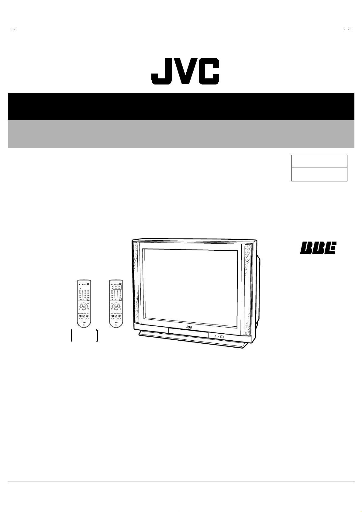
SERVICE MANUAL
COLOR TELEVISION
AV-27F703
AV-27F713
AV-27F803
BASIC CHASSIS
RM-C 326G
RM-C326
AV -2 7F70 3
AV -2 7F71 3
[RM-C 325G]
AV -2 7F80 3
AV-27F703
AV-27F713
AV-27F803
/S
/S
/S
GJ
(No.A111)
CONTENTS
! SPECIFICATIONS ・・・・・・・・・・・・・・・・・・・・・・・・・・・・・・・・
!
SAFETY PRECAUT IONS
!
FEATURES・・・・・・・・・・・・・・・・・・・・・・・・・・・・・・・・
! HOW TO IDENTIFY MODELS ・・・・・・・・・・・・・・・・・・・・・・・・・・・・・・・・
!
MAIN DIFFERENCE LIST
! FUNCTIONS ・・・・・・・・・・・・・・・・・・・・・・・・・・・・・・・・
! SPECIFIC SERVICE INSTRUCTIONS ・・・・・・・・・・・・・・・・・・・・・・・・・・・・・・・・
!
SERVICE ADJUSTMENTS ・・・・・・・・・・・・・・・・・・・・・・・・・・・・・・・・
! PARTS LIST ・・・・・・・・・・・・・・・・・・・・・・・・・・・・・・・・
★ OPERAT ING INSTRUCTIONS
★ STAND ARD CIRCUIT DIAGRAM ・・・・・・・・・・・・・・・・・・・・・・・・・・・・・・・・
1
・・・・・・・・・・・・・・・・・・・・・・・・・・・・・・・・・・・・・・・・・・・・・・・・・・・・・・・・・・・・・・・・
・・・・・・・・・・・・・・・・・・・・・・・・・・・・・・・・・・・・・・・・・・・・・・・・・・・・・・・・・・・・・・・・
・・・・・・・・・・・・・・・・・・・・・・・・・・・・・・・・・・・・・・・・・・・・・・・・・・・・・・・・・・・・・
・・・・・・・・・・・・・・・・・・・・・・・・・・・・・・・・・・・・・・・・・・・・・・・・・・・・・・・・・・・・・・・・
・・・・・・・・・・・・・・・・・・・・・・・・・・・・・・・・
・・・・・・・・・・・・・・・・・・・・・・・・・・・・・・・・・・・・・・・・・・・・・・・・・・・・・・・
・・・・・・・・・・・・・・・・・・・・・・・・・・・・・・・・・・・・・・・・・・・・・・・・・・・・・・・・・・・・・・・・
・・・・・・・・・・・・・・・・・・・・・・・・・・・・・・・・・・・
・・・・・・・・・・・・・・・・・・・・・・・・・・・・・・・・・・・・・・・・・・・・・・・・・・・・・・・・・・・・・・・・
・・・・・・・・・・・・・・・・・・・・・・・・・・・・・・・・・・・・・・・・・・・・・・・・・・・・
・・・・・・・・・・・・・・・・・・・・・・・・・・・・・・・・・・・・・・・・・・・・・・・・・・・・・・・・・・・・・・・・
・・・・・・・・・・・・・・・・・・・・・・・・・・・・・・・・
・・・・・・・・・・・・・・・・・・・・・・・・・・・・・・・・・・・・・・・・・・・・・・・・・・・・・・・
・・・・・・・・・・・・・・・・・・・・・・・・・・・・・・・・・・・・・・・・・・・・・・・・・・・・・・・・・・・・・・・・
・・・・・・・・・・・・・・・・・・・・・・・・・・・・・・・・・・・・・・・・・・・・・・・・・・・・・・・・・・・・・・・・
・・・・・・・・・・・・・・・・・・・・・・・・・・・・・・・・・・・・・・・・・・・・・・・・・・・・・・・・・・・・・・・・
・・・・・・・・・・・・・・・・・・・・・・・・・・・・・・・・・・・・・・・・・・・・・
・・・・・・・・・・・・・・・・・・・・・・・・・・・・・・・・・・・・・・・・・・・・・・・・・・・・・・・・・・・・・・・・
・・・・・・・・・・・・・・・・・・・・・・・・・・・・・・・・・・・・・・・・・・・・・・・・・・・・・
・・・・・・・・・・・・・・・・・・・・・・・・・・・・・・・・・・・・・・・・・・・・・・・・・・・・・・・・・・・・・・・・
・・・・・・・・・・・・・・・・・・・・・・・・・・・・・・・・・・・・・・・・・・・・・・・・・・・・・・・・・・・・・・・・
・・・・・・・・・・・・・・・・・・・・・・・・・・・・・・・・・・・・・・・・・・・・・・・・・・・・・・・・・・・・・・・・
・・・・・・・・・・・・・・・・・・・・・・・・・・・・・・・・・・・・・・・・・・・・・・・・
・・・・・・・・・・・・・・・・・・・・・・・・・・・・・・・・・・・・・・・・・・・・・・・・・・・・・・・・・・・・・・・・
COPYRIGHT © 2002 VICTOR COMPANY OF JAPAN, LTD.
・・・・・・・・・・・・・・・・・・・・・・・・・・・・・ 2
・・・・・・・・・・・・・・・・・・・・・・・・・・・・・・・・・・・・・・・・・・・・・・・・・・・・・・・・・・
・・・・・・・・・・・・・・・・・・・・・・・
・・・・・・・・・・・・・・・・・・・・・・・・・・・・・・・・・・・・・・・・・・・・・・
・・・・・・・・・・・・・・・・・・・・ 4
・・・・・・・・・・・・・・・・・・・・・・・・・・・・・・・・・・・・・・・・
・・・・・・・・・・・・・・・・・・・・・・・
・・・・・・・・・・・・・・・・・・・・・・・・・・・・・・・・・・・・・・・・・・・・・・
・・・・・・・・・・・・・・・・・・・・・・・・・・・・・・・・・・
・・・・・・・・・・・・・・・・・・・・・・・・・・・・・・・・・・・・・・・・・・・・・・・・・・・・・・・・・・・・・・・・
・・・・・・・・・・・・・・・・・・・・・ 12
・・・・・・・・・・・・・・・・・・・・・・・・・・・・・・・・・・・・・・・・・・
・・・・・・・・・・・・・・・・・・・・・・・・・・・・・・・・・・・・ 33
・・・・・・・・・・・・・・・・・・・・・・・・・・・・・・・・・・・・・・・・・・・・・・・・・・・・・・・・・・・・・・・・
・・・・・・・・・・・・・・・・2- 1
・・・・・・・・・・・・・・・・・・・・・・・・・・・・・・・・
・・・ 4
・・・・・・
・・ 6
・・・・
・・・・・・・・・・・・・ 8
・・・・・・・・・・・・・・・・・・・・・・・・・・
3
5
No.520 05
Jun. 2002
Jun. 2002
Page 2
A
V-27F703
A
A
V-27F713
V-27F803
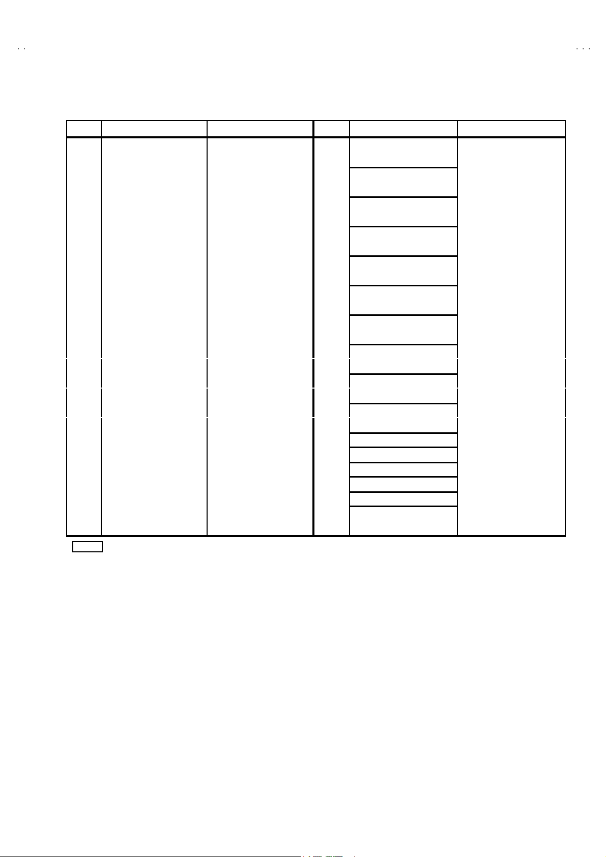
SPECIFICATIONS
Items Cont e nts
Dimensions (W
Mass 94.6 Ibs (4 3.0 kg)
TV System
and C olor S yste m
TV Receiving Channels
and Frequency
CATV Receiving Channels
and Frequency
Intermediate Fr equency Vide o IF Car rier
Color Sub Carrier 3.58MHz
Power Input 12 0V AC , 60H z
Power Consumption 14 0W
Pictur e Tube 27 ” (6 8cm ) M ea sured Diag on al l y
Hi gh Vo l t ag e
Speake r
Audio Power Out put 5W + 5W
Input terminals
Fix Audio Output 50 0m V( r ms) , ( -4dBs ), LOW Im pe dance ( 400 H z when mod ul a ted 100%)
AV compulink ⅢⅢⅢⅢ Input 3.5 m m mi ni jac k
Antenna terminal 75Ω(VHF/UHF) Terminal, F-Type Connector
Remote Control Unit RM-C 32 6G(AV-27F703) / R M- C32 6( AV- 27 F71 3) /R M-C32 5G (AV -27F8 03 )
××××H××××
D) 29 - 7/8 ”×23”-3/8”×19-3/4” (758mm×59 3m m×5 00m m)
TV RF Syste m
Color System
Sound System
VL B a nd
VH B and
UHF Band
Low Band
High Band
Mid Band
Super Band
Hy p er Band
Ul tr a B an d
Sub Mid Band
TV/CATV Total Channel 18 0 Cha nn el s
Sound IF Carrier
Input 1 (Rear) S-Video
Vide o
Audio (L/MON O, R)
Input 2 (Rear) Video
Component video
Audio (L/MON O, R)
Input 3 (Front) Video
Audio (L/MON O, R)
Input 4 (Rear)
(For AV-27F8 03)
Component video
Audio (L/MON O, R)
CCIR(M)
NTSC
BTS C S ys tem ( M ul ti -Ch an nel S ound )
(02~06) 54 MHz ~88MHz
(07~13) 17 4M H z~21 6M Hz
(14~69) 47 0M H z~80 6M Hz
(02~06, A-8) by (02~06&0 1)
(07~13) by (07~13)
(A~1) b y (14~22)
(J~W) by (23~36)
(W +1~W+28) b y (37~64)
(W +29 ~W +84) b y ( 65 ~1 25)
(A8, A4~A1) by (01, 96~99 )
45 .75 MHz
41.25 MHz ( 4 .5MH z)
30 .0 kV±1.3kV (at zero beam current)
2“×4 -3/ 4” ( 5×12 cm ) Oval t ype×2
Y : 1V(p -p ) P ositive ( N eg ativ e s ync p rovided, w h en term i nat ed with 75 Ω)
C : 0 .28 6V(
1V (p- p ), 75 Ω
50 0m V( r ms) ( - 4d Bs ), High Im pe dance
1V p- p, 75 Ω
Y : 1 V( p- p) P ositive ( N eg ati ve sync provide d, when ter m i na ted with 7 5Ω)
PB, PR : 0.7V(p-p), 75Ω
50 0m V( r ms) ( - 4d Bs ), High Im pe dance
1V (p -p ), 75 Ω
50 0m V( r ms) ( - 4dB s ), High Im pe dance
Y : 1 V( p- p) P ositive ( N eg ati ve sync provide d, when ter m i na ted with 7 5Ω)
PB, PR : 0.7V(p-p), 75Ω
50 0m V( r ms) ( - 4d Bs ), High Im pe dance
(AA/R 6 /UM- 3 bat ter y×2)
p-p
) (Burst si g nal , wh en te rmina ted with 7 5 Ω)
(54MHz~ 80 4MH z)
De sign & speci f icat ions ar e su bject to chang e wi th ou t notice.
2
No.52005
Page 3
A
3
A
3
A
3
SAFETY PRECAUTIONS
V-27F70
V-27F71
V-27F80
1. The d esi gn of t hi s p ro du ct c ont ai ns spec i al h ar dw ar e, man y
ci rcu its and co mp on ent s s pecial l y for saf ety purp oses. For
continued protection, no changes should be made to the
origi na l des ig n unl ess a uthor ized in wr iti ng by t he m an ufac tu re r.
Replacem en t parts must be ident ic al t o thos e us ed in th e
origi na l c ircui t s . S ervic e sho ul d be perf or me d b y qu al i fi ed
p ers onnel o nl y.
2. Alte r ati on s of th e des i g n o r circu i tr y of the p rodu cts s hou ld n ot
b e m ad e. A ny desi gn al te rations or ad di tio ns will vo id th e
manufacturer's warranty and will further relieve the
manu fact ur er of resp ons ib ilit y for pers ona l in ju r y or p rope rt y
d am age r esu lt in g t heref rom .
3. M an y electr i cal an d m ech an ic al pa rt s in th e produ cts h ave
sp ecial saf ety- r el at ed charact eris tic s. These charac teri stics ar e
oft en n ot e vid en t fr om v isu al in spe ction no r can t he prote ction
aff or de d by them n ecess ar ily be obtained b y usi ng
replac ement c o mp on ents ra ted for h ig her vo ltag e, wa ttag e, etc.
Replacem en t pa rt s whic h h av e t hes e sp ecial s afet y
ch aracteristi c s a re i d entified in th e par ts l ist of S ervic e m an ual.
Electrical components having such features a re identified
by shading on the schematics and by (!!!!) on the parts list
in S erv ice manual . The u se of a subst itute re plac emen t whi ch
does not have the same saf ety characteristics as the
reco mm en de d replac em en t pa rt s ho wn in the pa rts l ist of
Se rvi ce ma nu al m ay c ause sh ock, f ire, or o ther hazards.
4. Use iso la tio n tr an sf orme r when hot chassis .
The chassis and any sub-chassis contained in s ome products
are c on nect ed to one si de of th e AC p ower l i ne . An i sol a tion
tr ansf or m er of ad equ ate c ap ac ity sh ou ld be ins er t ed bet we en
th e p r odu ct and t he AC p ow er su pp ly p oint while p erfor ming
an y s er vic e on so me pr o duc ts when th e HOT c h assis is
exp ose d.
5. Don't shor t between the LIVE side ground and I SOLATED
(NE UTRAL) side ground or EARTH side ground when
repairing.
So m e m od el 's p ower c irc uit is par t ly di f feren t in t he GND. Th e
diff er enc e of t he GND is sh ow n by th e LI VE : (") side GND,
th e ISO LATED( N EUTRA L) : (#) s ide GN D an d EAR TH : ( $)
si de GND . Don 't sho rt be tween t he LIVE s id e GN D a nd
ISO LATE D(N EUTRAL) side GND or EARTH si de GND and
never measure with a measuring apparatus (oscilloscope etc.)
th e LI VE side GND a nd ISO LATED(N EU TRA L) si d e G ND or
EARTH side GND at the s ame time.
If above note will not be kept, a fuse or any parts will be broken.
6. If any repa ir h as b een m ade to th e chass is, it is re c ommend ed
th at t he B1 se ttin g sh ou ld b e chec ked or adjuste d (S ee
ADJUST M ENT OF B 1 POW E R SUPPL Y).
7. The hig h volt ag e app lied t o the pictu re tube mu st co nform wi th
that specified in Service manual. Excessive high voltage can
cau s e an incr ea se i n X-Ra y emi ssi on , a rci n g and p ossi bl e
com po ne nt d am ag e, th er ef ore op er ati o n un der excess i ve hi gh
vol ta ge c ond it i ons sh ou ld be k e pt to a m in imum, or sh ould be
preve nt ed. I f s evere arc in g occu rs, r em ov e th e AC p ower
immediately and determine the cause by visual inspection
(inc or r ect installa tion , crac ked o r melte d hi gh voltag e h ar nes s,
p oor s olde rin g, etc. ). T o mainta in the pr op er minim um le vel of
soft X-Ra y emission, components in the high voltage circuitry
incl ud i ng the picture tu be mus t be the ex a ct r ep l acemen ts or
alte rn at ives appr o ved b y th e manuf actu r er of th e co mp l ete
prod uct.
8. Do n ot c hec k hi gh vol ta ge by d r aw in g a n ar c . U s e a hi gh
vol ta ge m ete r or a hi gh volt age pro be wi th a VT VM . Di sc h ar ge
th e p ictu r e tu be bef or e a tte mp ting meter co nne cti on , b y
con nec ting a c lip lead t o th e gr ou nd fr am e a nd con n ecti ng t he
oth er e nd of t he lead th roug h a 10kΩ 2W resist or to t he anode
bu tto n.
9. W hen s e rvi c e i s required, ob s er ve th e o rig in al l ea d dr es s.
Extra p r ecau tion sh ould be given t o assu re cor re ct lea d dr es s
in the h i gh v olta ge c ircu it ar ea . W her e a sh ort cir c ui t ha s
occu rre d, th ose c omp on en ts th at i nd ic ate ev iden ce of
overheating should be replaced. Always use the
manu fact ur er 's replace m ent compon ents .
10 . Isolation Check
(Safety for Electrical Shock Hazard)
Af ter re-a ssem bl ing th e pr od uct , always pe rf or m an iso lation
ch ec k on th e expo s ed m etal p ar ts of the c abin et ( ant en na
ter m ina ls, vi de o/a ud i o in pu t and out put t er mi n al s, Con tr ol
knobs, metal cabinet, screwheads, earphone jack, control
sh afts, etc .) to be sure th e pr o duct is saf e t o op er at e w i th out
d ang er of elect rica l shoc k.
(1) Di electric Strength Test
The is olat ion b etwe en the AC pri ma r y cir cu it and al l m eta l parts
exp osed t o th e us er, par ticu larly an y expo sed m etal p art h aving
a re tur n pat h to the ch assi s sh ou ld w i ths t and a volta ge of
11 00V AC ( r .m.s.) f or a p eriod of one s ec ond.
(. . . . Withstand a voltage of 11 00V AC (r.m. s.) to an applian ce
rate d up to 120V , a nd 3 000V AC ( r .m. s.) t o an appl i anc e ra ted
200V or more, for a period of one second.)
Thi s meth od of tes t re qu ires a t est eq uip me nt n ot g en er al l y
fou nd in t he servi ce t ra de.
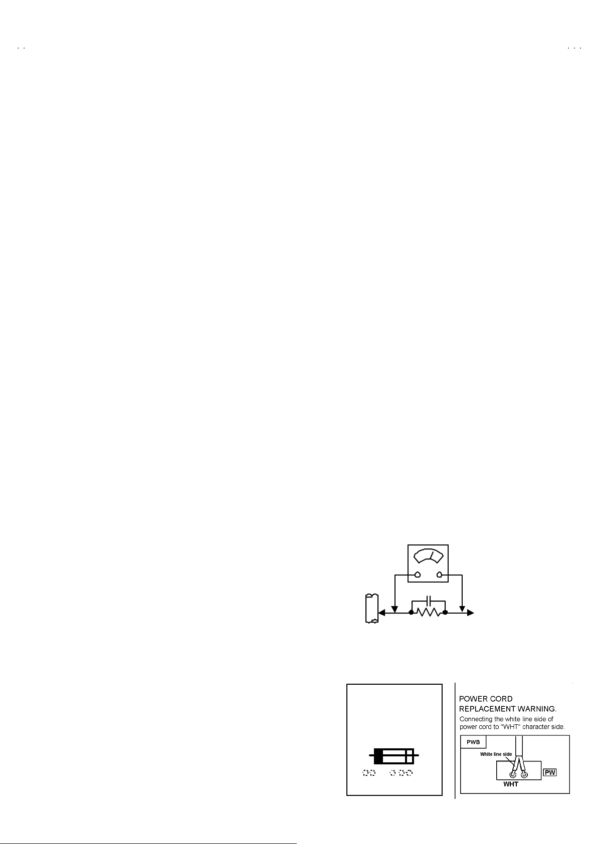
(2) Leakage Current Check
Plug t he A C line c ord direct ly int o th e AC ou tl et ( do not u s e a
line is olation tra nsf orm er dur i ng t his che ck.) . Using a " L eakage
Curr ent Tes t er", mea sure t he lea kag e cur r en t fr om each
exp os e d m etal part of th e ca bine t, partic ul ar l y an y expo s ed
metal part having a retur n path to the ch assis, to a known good
ea rt h gr o und (water p ipe, etc.). A ny lea kag e cur r en t must not
exce ed 0. 5mA AC ( r.m. s.).
Howev e r, i n t ropical a r ea, thi s m us t not e xc eed 0 .2m A AC
(r.m.s.).
"""" Altern at e Che ck M ethod
Plug t he A C line c ord direct ly int o th e AC ou tl et ( do not u s e a
line isolation transformer during this check.). Use an AC
vol tm et er h aving 100 0 o hm s per vol t or more sen s iti vit y in the
follo win g manner. C on nec t a 150 0Ω 1 0W r esistor pa ralle l ed
by a 0.15μ F AC-typ e cap ac i tor b etween an exp ose d meta l
p art and a kno wn g o od ear th gr ou nd (wate r pipe, et c.).
Measu r e th e A C voltag e ac r oss th e resi st or w it h t he AC
voltmeter. Move the res istor connection to each exposed metal
part, particularly any exposed metal part having a return path to
th e ch assis , an d m ea s ur e t he A C vol ta ge acr os s th e r esis to r.
Now, reve rs e th e pl u g in t he A C out let a nd r ep e at e ach
measu r em en t. An y volta ge me as u re d m ust not exce ed 0.7 5V
AC (r.m. s.) . This corresp on ds t o 0 .5mA AC (r.m. s.) .
Howev e r, in tropic al ar ea, this m ust n ot exc ee d 0 .3V AC
(r.m.s.). T his corr esponds to 0.2m A AC ( r.m.s.).
AC VOLT METER
(HAVING 1000 Ω/V,
GOOD
EARTH
GR OUND
11 . High voltage hold down circuit check.
Af ter rep air of the hi gh volt ag e h old down ci r cuit, th is circu i t
sh all be c hecked to op er ate corr ectly.
See ite m "Ho w to check the high voltage hold down
cir cuit".
This mark shows a fast
operating fuse, the
letters indicated below
show the r ati ng.
0.15μF AC-T YPE
1500Ω 10W
OR MOR E SENSIT IVITY)
PLACE THIS PROBE
ON E A C H EX PO SE D
ME T AL PA RT
A V
No. 52005
3
Page 4
A
V-27F703
A
A
V-27F713
V-27F803
FEATURES
New chas s is design en abl es use of a si ngl e boar d with si mp lif ied
"
circuit ry.
User s can make f un to co nnect the D VD pl ayer wit h the compon ent
"
vid eo signal i npu t termi na l.
Provid ed w ith miniatu re tuner (TV/C ATV ).
"
Multif unct ional rem ote con tro l p erm its pic tu re a djustment.
"
Ad opti on of the CHANN EL GUAR D fu ncti on pr events th e s peci fic
"
chan nels from being selected, unl ess th e “ID nu mbe r” is k ey in.
2
"
I
C bus control utilizes single chip ICs.
"
Adoption of the VIDEO STATUS / TH EA TER PRO. fu nction.
"
Adoption of the ON /OFF TIM ER and SLE EP TI MER fu nction .
Built-in V-CHIP system.
"
Clos ed- caption b roadcas ts can be view ed.
"
Built- in MTS sys tem , B BE / HYPER- SU RROUND system.
"
"
S-VIDEO in put termi nal for tak i ng best advantag e of S uper VH S .
"
Dig it al Com b fil ter Improved pictur e quality.
"
Bu ilt-in EZ SURF system.(AV-27F8 03)
By pus h in g the E Z SURF key, B ack Pro gra m Inf ormation can be
displ ayed in written fr om pr ogr am Inf ormation us es a CAL L
LE TTER (br oadca sting stati on ID ) , a Netw or k name and a
Program name of XD S d ata, an d collec t’ s tu ni ng of the tune r f or
PIP one by one.
HOW TO IDENTIFY MODELS
• How to recognize from the appearance of the model concerned is written below. Please distinguish from several contents
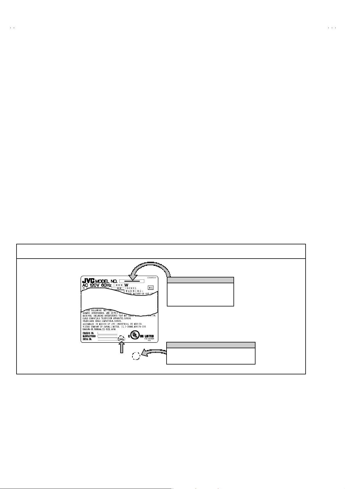
curre ntly prin ted on the r ating label.
[RATING LABEL]
Indicated
AV -27 F703
AV -27 F713
AV -27 F803
Distinguish
INDICATED “S”
Please d ist in gui sh fr om sev era l conten ts
cur r entl y printed on t he Rati ng Label .
4
No.52005
Page 5
A
A
A
MAIN DIFFERENCE LIST
V-27F703
V-27F713
V-27F803
!!!!
Parts Name
MAIN PW B SGJ -1004A -M2 SGJ -1003A -M2 SGJ -1002A -M2
PIP PW B ××SGJ -4001A -M 2
AV SEL PWB SGJ -5002A -M2 ← SGJ -5001A -M 2
3D Y/C S EP M OD ULE PWB
! FR ON T CABI. A SSY LC10878 -0 03B- A LC10878 -0 04A- A LC10 878 -0 03B- A
JVC M AR K CM48006 -008- C C M4 8006 -0 09- C CM48006 -008- C
! DOOR LC20628 -0 01C -A LC20628 -0 02A- A LC20628 -0 01C -A
!
KNOB (P OWER) LC31 237 -0 01A- A LC31 237 -0 02A- A LC 31 237 -0 01A- A
OPE RATION SH EE T LC31 238-0 04A- A LC 31 238 -0 05A- A LC31238 -0 04A- A
!
CONTR OL K NOB LC20217 -0 04B- A LC20217 -0 06A- A LC20 217 -0 04B- A
!
TERM INA L BOARD LC20899 -0 04A- A LC20899 -0 04A- A LC20 899 -0 05A- A
REMO CO N UNIT RM-C 326 G-1A RM-C 326 -1 A RM- C 325 G-1A
INPUT TER MINAL INPUT1~INPUT3 ← INPUT1~INPUT4
Model name
AV-2 7F 70 3/S AV-2 7F 71 3/S AV-2 7F 80 3/S
××
SGJ 0Y001A-M2
No.52005
5
Page 6
A
V-27F703
A
A
)
(Y,
,
)
V-27F713
V-27F803
FUNCTIONS
■■■■
FRONT PANEL CONTROL
2
1
3 6
5 8
4
1INPUT3 VIDEO termi nal 6VOLUME -/+ buttons
7 9
2
INPUT3 AUDIO L / MONO terminal
7
SENSO R RE M OT E CON TR OL
3INPUT3 AUDIO R ter minal 8ON TIMER LED
4
MENU button (▼)
5
CHANNEL -/+ buttons
OPERATE / butt ons (use MENU screen)
■
REAR TERMINAL
[[[[
AV -2 7F7 03 /S, AV-27F713/S ]
1
2
3
4 5
9
POWER button
1
2
3
4
[[[[
AV -2 7F8 03 /S ]
5 6
AV-27F703/S, AV-2 7F 713/S ]
[[[[
1
INPUT 1 (S-VIDEO, V, L/MONO, R) terminals
2INPUT 2 (V, L / MONO, R) terminals
/ COMPONENT VIDEO(Y, P
3
AUDIO OUT(L, R) terminals
4
AV CO MPULIN K
Ⅲ
B
, PR) terminals
5 VHF / UHF terminal
6
No.52005
AV-27F803/S ]
[[[[
1
INPUT 1 (S-VIDEO, V, L/MONO, R
terminals
2
INPUT 2 (V, L / MONO, R) terminals
/ COMPONENT VIDEO(Y, P
3
INPUT 4 (L, R) terminals
/ COMPONENT VIDEO
B
, PR) terminals
B
R
P
P
terminals
4AUDIO OUT(L, R) terminals
5
AV CO MPULIN K
6
VHF / UHF termi nal
Ⅲ
Page 7

AV-27F703
AV-27F713
AV-27F803
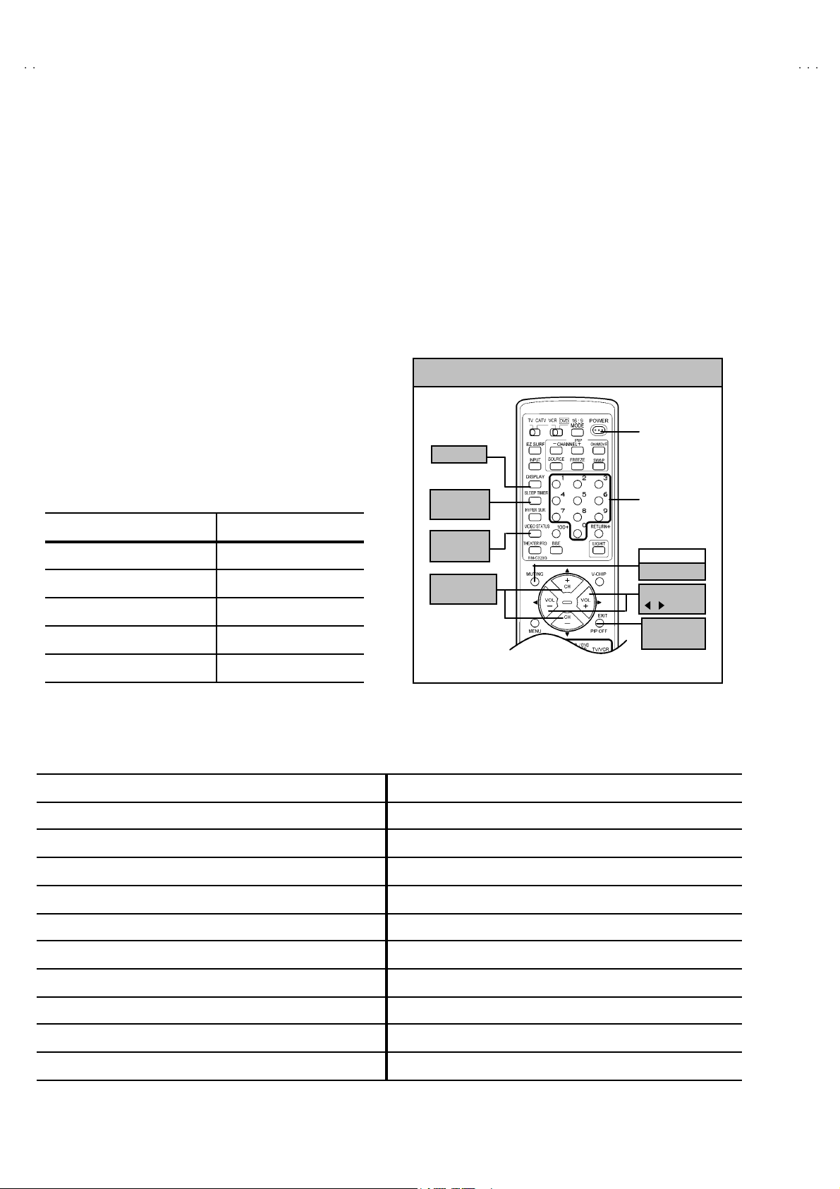
■REMOTE CONTROL UNIT
RM-C326G : AV-27F703
RM-C326 : AV-27F713
1 2 3 4
5
6
7
8
9
10
11
12
13
14
/S
/S
15
18
19
20
21
17
16
1TV / CATV switch
2VCR / DVD switch
316 : 9 MODE Key
4POWER Key
TV VIDEO1 VIDEO2 VIDEO3
5INPUT Key
( )
6DISPLAY Key
0 15 30 ……165 180
7SLEEP TIMER Key
( )
8HYPER SUR. Key ( Can be changed ON / OFF )
9VIDEO STATUS Key
ATHEATER PRO key
BBBE key ( Can be changed ON / OFF )
CMUTING Key
DFUNCTION Key ( CH -/+ / VOL -/+ )
The FUNCTION keys operate CHANNEL and VOLUME normally.
These keys are also used to navigate MENU system.
EMENU Key
FNUMBERS Key
G100+ Key
HRETURN+ Key
ILIGHT Key
JV-CHIP Key
KEXIT Key
LVCR / DVD Keys
[RM-C325G : AV-27F803/S]
1 2 3 4
23
5
6
7
8
9
10
11
12
13
14
22
16
18
19
20
21
15
17
1TV / CATV switch
2VCR / DVD switch
316 : 9 MODE Key
4POWER Key
TV VIDEO1 VIDEO2 VIDEO3 VIDEO4
5INPUT Key(
)
6DISPLAY key
0 15 30 ……165 180
7SLEEP TIMER Key
( )
8HYPER SUR. Key ( Can be changed ON / OFF )
9VIDEO STATUS Key
ATHEATER PRO key
BBBE key( Can be changed ON / OFF )
CMUTING Key
DFUNCTION Key ( CH -/+ / VOL -/+ )
The FUNCTION keys operate CHANNEL and VOLUME normally.
These keys are also used to navigate MENU system.
EMENU Key
FNUMBERS Key
G100+ Key
HRETURN+ Key
ILIGHT Key
JV-CHIP Key
KEXIT / PIP OFF Key
LVCR / DVD Keys
MPIP Key
NEZ SURF Key (Back Program Information can be displayed.)
No.52005
7
Page 8

A
V-27F703
A
A
V-27F713
V-27F803
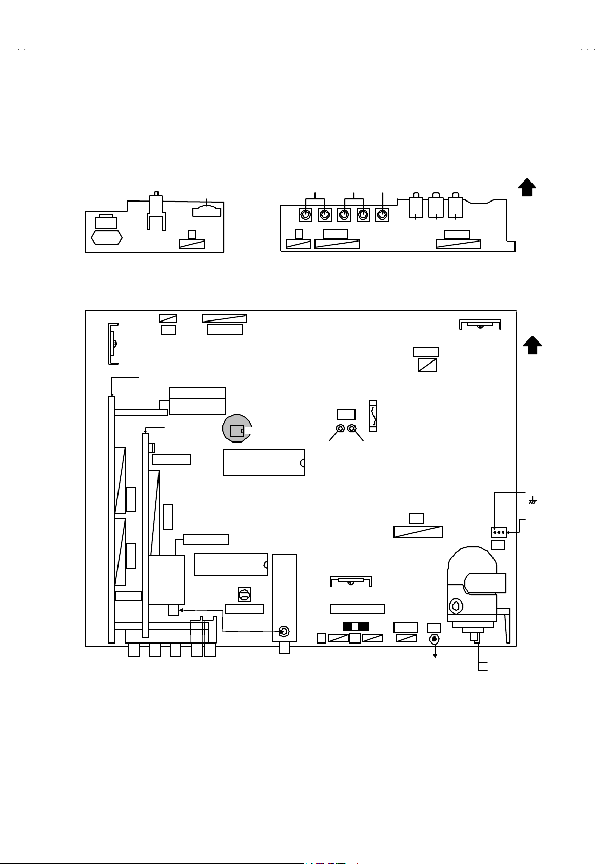
SPECIFIC SERVICE INSTRUCTIONS
DISASSEMBLY PROCEDURE
REMOVING THE REAR COVER
1. D isc onnect t he po w er plu g f ro m wa ll out le t.
2. As s hown i n th e Fig .1, rem o ve th e 12 screws marked
3. W i thdr a w t he r ear c over b ackw ar d.
!!!!
.
CHECKIN G THE CHASSIS
To check the PW Board fro m back side.
1. Pu ll out the ch assis (re fer t o REM OVI NG THE CHA SSIS) .
2. Erect th e c has sis ver ti ca lly so th at y ou can ea sil y check th e bac k
si de of the PW Boar d.
REMOVING THE TERMINAL BOARD
" After removing the rear cover.
1. As s hown i n Fig.1 , r emo ve t he scre ws ma rked
2. Withdraw the terminal board toward you.
""""
.
REMOVING THE CHASSIS
" After r emovi ng the rear c over / terminal board .
1. Sl i ght ly r ai se t he both si d es of c h assi s b y hand an d r em o ve th e
claws u nder th e both sid e of th e ch assis from th e front cabi net.
2
2. W i thdr a w t he c hass is backw a rd .
(If n ecess ary , r em ove t he wire clamp, c onnec t ors etc.)
REMOVING THE SPEAKER
" After removing the rear cover.
1. A s shown i n Fig. 1 , re mo v i ng th e 4 scr ews m ar k ed
remove the sp eaker.
2. Follow th e s ame st eps wh en r em oving th e oth er ha nd sp eak er.
NOTE : When removing the 4 screws mark ed
remove t he lower si de s cr ew f irs t, and th en remove th e
up per one .
####
####,
of th e s p eak e r ,
REMOVING THE LED & POWER SW PWB
"
After removing the rear cover & terminal board.
1. R em ove t h e 2 screws ma rked
2. Withdra w t he LE D & P OW ER SW PW B t oward yo u .
* If nec essary, remo ve th e wire clamp, connecto r etc.
as s hown in Fig. 1.
$$$$
then
[CAUT ION]
"
When e r ec ti ng th e ch assis, be car ef ul so tha t there will b e no
contacting with other PW Board.
"
Be for e tu rn ing o n p ower , make s ur e th at t he w i r e connec tor is
prop er ly c on nec ted .
"
When conducting a check with power supplied, be sure to
confirm that the CRT EARTH WIRE (BRAIDED ASS’Y) is
connected to the CRT SOCKET PW board.
WIRE CLAMPIN G AND CABLE TYING
1. Be sure t o clamp th e wire.
2. Never remove the c able tie use d f or tying th e wi res togethe r.
Should it b e inadverte ntly removed, be sure to tie the wir es with a
new cable tie.
REMOVING THE FRONT CONTROL PWB
" After removing the rear cover & terminal board.
1. R em ove t h e 2 screws ma rked
2. Withdraw the FRONT CONTROL PWB toward you.
* If nec essary, remo ve th e wire clamp, connecto r etc.
8
as s hown in Fig. 1.
%%%%
No.52005
Page 9

A
3
A
3
A
3
FRONT CABINET
SP EAKER
CRT SOCKET
PWB
FRONT CONTROL
Thi s e xplod ed v i ew describe s a bout th e AV -27F 8 03/S.
Yo u c an use the explo ded view for d i sasse mb ling t he
AV -2 7F70 3
this one .
/S
AV -2 7F71 3/S in t he s ame st ep a s f or
C
(×4)
PWB
V-27F70
V-27F71
V-27F80
LED & POWER SW
PWB
3D Y/C SE P MODULE
REAR COVER
AV-27F803
PIP PW B
AV-27F803
E
(×2)
/S
CHASSIS
CLAW
MAIN PWB
D
(×2)
POWER CORD
/S
CLAW
AV SE LEC TOR
PWB
TERMINAL
BOARD
B
(××××6)
AV-27F803
(××××4) AV-27F703
AV-27F713
/S
/S
/S
A
(×12)
Fig .1
No.52005
9
Page 10
A
V-27F703
A
A
)
S
▼/
S
US
V-27F713
V-27F803
MEMORY IC REPLACEMENT
1. Memory IC
This TV uses memory IC.
Thi s memory IC s t ores dat a for prop er o pera ti on of the vide o and deflecti o n cir cuits.
When r ep la cing t he m em or y IC , be sure to use an IC c o nta ini ng th is (initia l value ) d ata.
2. Memory IC replacement procedure
(1) Power off
Switch off th e p ow er a nd disc onn ect t he power co rd from t he w al l
ou tl et.
(2) Replace the memory IC
Be sure t o use a memory I C wri tte n with the initi al settin g data.
(3) Power on
Con nect the power cor d to the wall outle t a nd switc h o n the power.
SE RVICE M EN U
SERVICE MENU
1. V/C(S ) 2. DEF(D)
3. SOUND(A) 4. OTHERS (F)
5.PIP(PIP) 6.3L Y/C(LYC)
7. LOW LI GHT 8. HIGH LIG HT
9.RF AFC 10.VCO
2
C BUS 12.SYSTEM(SYS)
11. I
AV-27F803
6.3D Y/C(DYC)
Verified
/S
(4) Co nfir m the syst em const ant value
"
12 .S YSTEM (SYS ) do not a dj ust normally .
"
The adjustment should not be done without signal.
! Ho w to enter the SERVICE MENU.
1) Press the SLE EP TIM ER key and set SLE EP TIME R for 「0 m i n」.
2) Be for e di sap pe ar the dis pla y of SLE EP TIMER settings,
si mu lt an eously pr ess the DISPLA Y key and VI DE O STAT US key o f
the remote c ontrol unit.
3) The SERVICE MENU screen will be displayed as shown Fig. 1.
!
Ho w to enter the 12. SYSTEM(SYS).
1) While the SERVICE MENU is displayed, select the
12.SYSTEM(SYS) item with FUNCTION (▼/▲) keys, and the
FUNCTION ( / ) keys is pressed, the screen will be displayed as
sh own i n F i g.2 .
5) R efe r to t he SY STEM ( SY STEM CONSTANT) TABL E 1 an d ch eck
the setting ite ms. If the value is d ifferent, select the s etting it em w ith
the FUNCTION ( ▼ / ▲) keys and adjust the setting with the
FU NCTION( / ) k eys . (Th e l ett ers of t he s elect ed ite m ar e
displayed in yellow. )
6) W hen ad jus tm ent has com pl et ed, th e va lu es st ore int o m em or y IC
automatically
7) Press the EXIT key to return the SERV ICE MENU screen.
8) T he n p ress th e EXIT key ag ai n to r eturn the n orm al scr een .
ELECT BY
OPERATE BY EXIT BY
EXIT
Fig.1
12.S YSTEM(SY S
SETTING ITE M
***SYS0 1 VID EO I N
SETTING No SETTING V ALUE
Fig. 2
KEY ASSIGNMENT OF REMOTE CONTROL UNIT
(RM-C325G)
POWE R
DISPLA Y
(5) Receive the channel setting
Refer to the OPERATING INSTRUCTIONS (USER'S GUIDE) and
SLEEP
TIMER
NUMBER
set the rece ive c h ann els ( Cha nn el s Prese t) as desc ribe d.
VIDEO
(6) User se tt in gs
Check th e us er sett in g it ems acc ordi ng to TABL E 2 .
Where thes e do no t agr ee , refer to th e O PE RA TIN G
INSTRUCTIONS (USER'S GUIDE) a nd set the ite ms as d escrib ed .
TAT
FUNCTION
▲
MUTIN G
ME MO RY
FUNCTION
/
EX IT
(7) SERVICE MENU setting
PIP OFF
Verify what to set in the SERVICE MENU, and set whatever is
necessary( Fig.1) .
Refe r to t he SERVI CE ADJ USTM ENT f or s etting.
NOTE
Alth ou gh des ign i s d i ffer ent, eac h r em ot e c ontr oller
has the same control function.
10
No. 52005
Page 11
A
3
A
3
A
3
12.SYS TEM(S YS) 【Syst em Con stant se tting】
Initial set ting v al ue Initial set ting v al ue
No. Setting item
AV-27F803
/S
AV-27F703
AV-27F713
/S
No. Setting item
/S
AV-27F803
/S
AV-27F703
AV-27F713
SY S01 VIDEO IN 04 03 SY S13 HYP SU RR 01 01
SY S02 PIP 01 00 SY S14 16:9 MD 01 01
SY S03 3D Y/ C 01 00 SY S15 HYP S CA N 01 01
SY S04 Y CV 01 01 SY S16 EZ SU RF 01 00
SY S05 CCD P CHK 01 01 SY S17 ID DISP 01 01
SY S06 PURIT Y 00 00 SY S18 C OMP ULINK 01 01
SY S07 VM 01 01 SY S19 C CD 01 01
SY S08 NOISE CR 01 00 SYS20 VCHIP 01 01
SY S09 CLR TEMP 01 01 SY S21 VC H IP CA 01 01
SY S10 TH EATE R 01 01 SY S22 JVC L OGO 01 01
SY S11 TH EATE R PRO 01 01 SY S23 CMP IN 01 01
SY S12 BB E 01 01 SYS24 CXA1 87 5 00 00
Table 1
User setting
Setting item Setting value Setting item Setting value
Use remo t e control ler keys
POWE R
CHANNEL
VOL UME
TV/V IDEO
OFF
Cable-02
10
TV
DISPLA Y
VIDEO STAT US
H YP E R S U RROU N D
BB E
PIP SOURCE
Settings of MENU
PICTURE MENU INITIAL SETUP MENU
STANDARD
LA NG U AGE
TIN T CEN TER FR ONT PAN EL LO CK OFF
COLOR CEN TER V2 COMPONEN T-IN NO
PICTURE CENTER+14 AUTO SHUT O FF OFF
BRIGHT CENTER CLOSED CAPTIO N OFF (CC1 / T1)
DETAIL CENTER AUTO TUNER SET UP Unnecessary to set
+ 14 (A V-27 F8 03/S)
+ 10 (A V-27 F7 03
/ AV-2 7F713/S)
/S
COLOR TEMPERATURE LOW CHANNEL SUMMARY
NOISE MUTING ON V-CHIP OFF
SOUND ADJUST MENU SE T LOC K C OD E (000 0) Unn eces sary to set
BA SS
TR EBL E
BALANCE
MTS
CENTER
CENTER
CENTER
STEREO
XDS I D
CLOCK / TIMERS MENU
SE T CL OC K
MA NUA L
TIME ZONE : PA CI FIC
D.S.T. : OFF
ON / O FF TIMER
OFF
Table 2
OFF
DYNAMIC
OFF
ON
Cable-04
(A V-27 F803/S)
ENG
Se tting Ch ann el
Gu ar d ch an ne l : All OFF
ON
V-27F70
V-27F71
V-27F80
/S
/S
No. 52005
11
Page 12
A
V-27F703
A
A
Y
▼/
/
V-27F713
V-27F803
SERVICE ADJUSTMENTS
ADJUSTMENT PREPARATION
1. You ca n ma ke the n e ce ssa ry ad ju st me nts f or th is u n it with
either the Remote Control Unit or with the adjustment tools
and parts as given below.
2. Ad justment with the Remote Control Unit i s made on the
basis of the initial setting values, however, the new setting
values which set the screen to its optimum condition may
differ f rom th e initial settings.
3. Make sur e that AC power is tu rned o n correc tly.
4. T ur n on the pow er for s et an d tes t eq ui p ment bef or e use , and
start t he adj ustm en t proced ures aft er w ai ti ng at least 30 min ut es.
5. U nl ess o the r wis e s pec ified, pr ep ar e t he mo st su itab le r ecep tion
or inp ut si gn al for adj ust m ent.
6. Never touch any adjustment part w hi ch ar e not spe cified in th e
list for t his adjustment - variable res istors, transformers, initial
set ti ng val u e, etc.
7. Pres etti ng b efore adj ustm en t.
Unles s ot her wise spec ified in t he a dj ustme nt i nstr uct i ons, p r es e t
th e f ollo wing f un ctions with th e re mo te c ont ro l un it :
User menu preset value
MENU ITEM PR ES ET
VIDEO STAT US STA NDAR D
BA SS, TREB LE, BA LANCE C EN TER
HYPER SURROUND OFF
TINT, COLOR,
PICTURE, BRIGHT , DETAIL
MTS ST ERE O
CENTER
ADJUSTMENT EQUIPMENT
1. DC voltmet er (or digital voltmeter)
2. Oscilloscope
3. Si gn al g en er at or (P attern g en er at or)[NTSC
4. Remote control unit
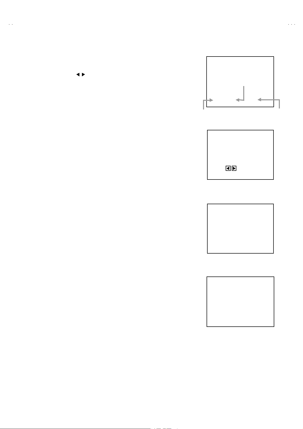
5. T V a ud io m ulti ple x si gn al ge ne rator .
6. F r equ enc y c ou nte r
FUNCTION
]
KEY ASSIGNMENT OF REMOTE CONTROL UNIT
(RM-C325G)
POWE R
DISPLA
SLEEP
TIMER
VIDEO
STA TUS
▲
NUMBER
MUTIN G
ME MO RY
FUNCTION
EX IT
PIP OFF
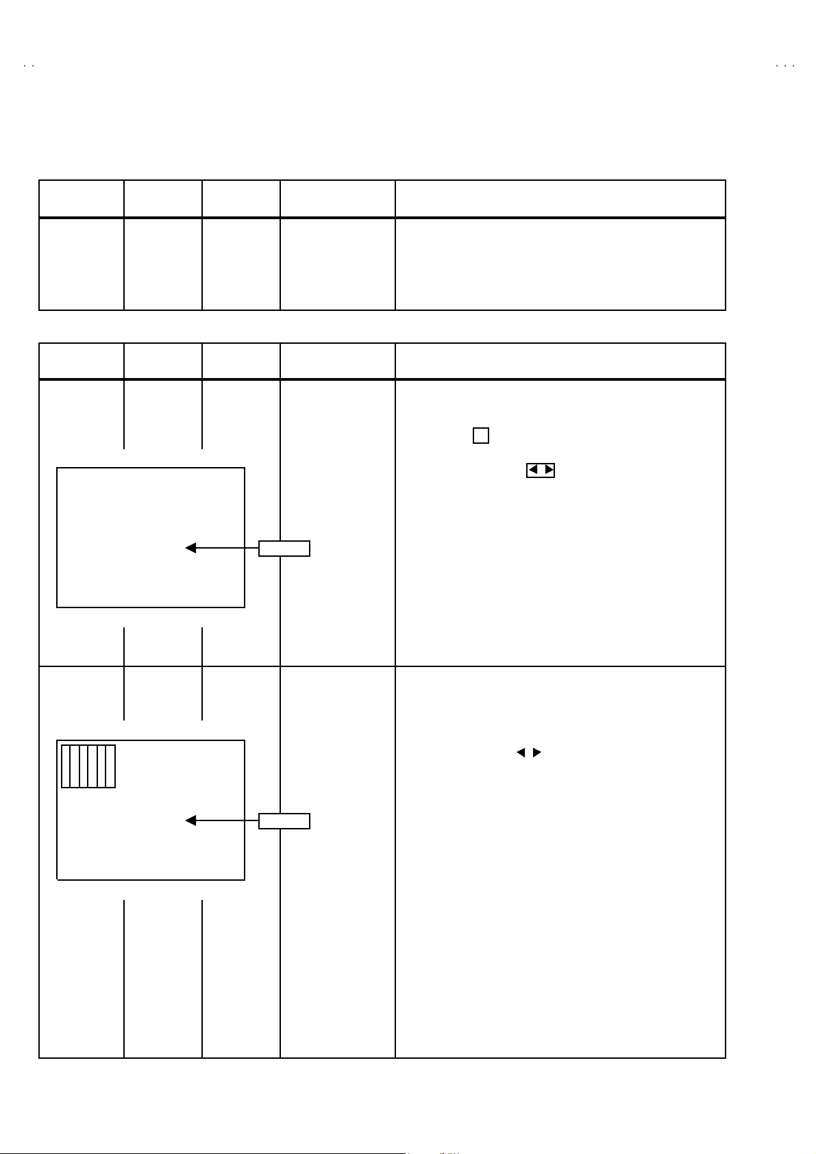
ADJUSTMENT ITEMS
%
C HECK OF B1 POW ER SUPPL Y
ADJU ST M EN T OF VCO WHITE BA LAN C E( H ig h Li ght & Lo w L igh t) ad ju s tm ent
%
MAIN VC O adj ust me nt PIP W HITE BALA NCE ( H igh Light ) adju stmen t
SUB VC O ad ju stm ent SUB B RI GHT adjust me nt
RF. AGC adjustment SUB CONTRAST adjustment
FOCUS adjustment SUB COLOR adjustment
%
ADJUSTMENT DEF CIRCUIT SUB TINT adjustment
%
V. HE IGH T / V. CENTER(4:3) adjustment
V. HE IGHT / L. LIN ( 1 6:9) adju stm ent MTS INPU T L EVE L adj us t me nt
H. POS I, H . SIZ E & S IDE P IN [ ( 4: 3) &(16: 9 ) ] a djustm e nt MTS SEP ARATIO N adjustment
PIP DISP LAY POS I adjus tm ent
12
%
ADJUSTMENT OF VIDEO / CHROMA CIRCUIT
%
ADJUSTMENT OF MTS CIRCUIT
HOW TO CHECK THE HIGH VOLTAGE HOLD DOWN CIRCUIT
%
No. 52005
Page 13
A
3
A
3
A
3
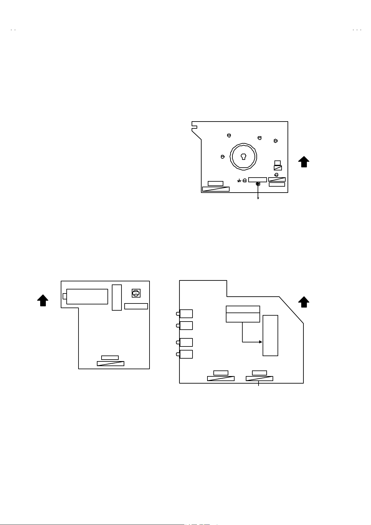
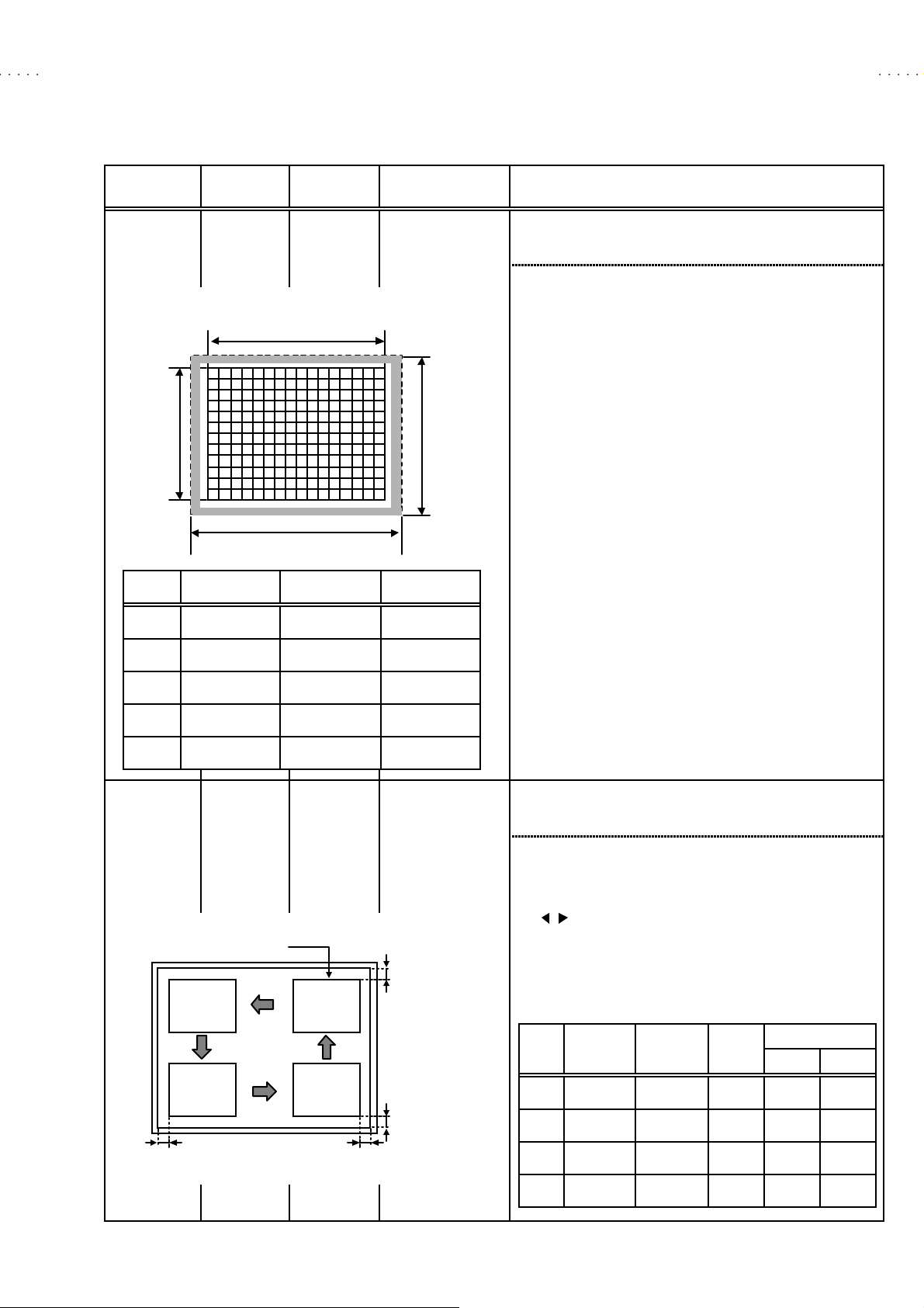
ADJUSTMENT LOCATIONS
V-27F70
V-27F71
V-27F80
LED & PW SW PWB
POWER
LED
SS
AV- 27F 803
3D Y/C SEP
MODULE
PI P P W B
(AV -2 7F803
B B
POWER
SW
S7701
D 770 1
IC62 1
AV SE LEC TOR PWB
T41 1
only)
/S
SUB VC O
SENSOR
I C7701
ONLY
/S
only)
/S
CN 007
IC70 2
MAIN PWB
me mo ry IC
IC20 1
FRONT AV IN PWB
CN 600 7
PW
WHT BL K
MENUVOL CH
F90 1
J6 403 J6 402 J6 401
CN 600 6
DEG
IC91 1
FRONT
FRONT
CN 003
(AV -2 7F803
CN 500 1 CN 500 3
CN 400 2
PIP T UNER/IF
IC10 1
T11 1
MAIN VCO
TUNE R
C
IC42 1
V CENTER SW
S421
S1
HV
CN 005
CR T EAR TH
(BRAIDED ASS'Y)
TP-E
( )
B1
(TP-91)
13
B1
HVT
HVT
HVTHVT
E1
UPPER : FOC US
LOWER : SCREEN
No. 52005
13
Page 14
A
V-27F703
A
A
(
)
V-27F713
V-27F803
CRT SOCKET PWB
TOP
PIP PWB
PIP T UNER
AV-2 7F80 3
IC
/S
T41 11
SUB VC O
CN 300 4
TP-G
71
TP-R
TP-E( )
TP-B
CN 30E2
CRT EARTH
(BRAIDED ASS'Y)
AV SELECTOR PWB
J5 501
J5 502
AV- 27F 803
3D Y/C SEP
MODULE
ONLY
/S
TP-E2
1
TP-E1
V
CN 300 5
TOP
6
TOP
14
CN 400 2
No. 52005
J5 504
(AV -2 7F803
J5 503
)
/S
CN 500 1 CN 500 2
(AV -2 7F803
)
/S
Page 15

A
V-27F70
3
A
3
A
3
5
/C(LYC)
Y
S
US
/
V-27F71
V-27F80
BASIC OPERATION OF SERVICE MENU
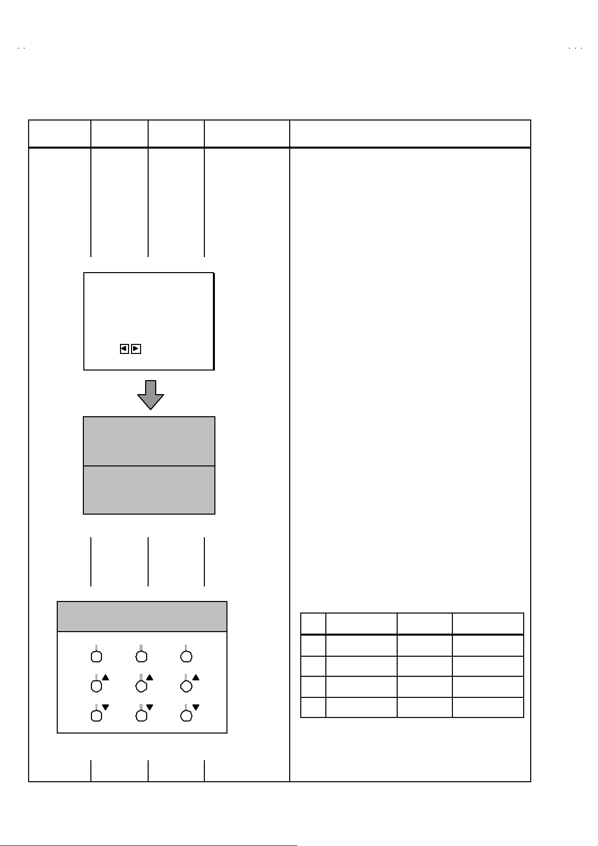
1. TOOL OF SERVICE M ENU OPERATION
Operate the SERVICE MENU with the REMOTE CONTROL UNIT.
2. In general, basic setting (adjustments) items or verifications are performed in the SERVICE MENU.
(1) V/C (S) ・・・・・・・・・・・・・・・・・・・・ ・・・・・・・・・・・・ ・・・・ This set the s ettin g values (a djustm e nt values) of th e VIDEO/ CHROMA circuits.
(2) DEF (D)
(3) SOUND (A) ・・・・・・・・・・・・・・・・・・・・ ・・・・・・・・・・・・ This set th e s etting valu es (adjustment va lues) of the AUDIO circuit.
(4) OTHERS (F)
(5) PIP (PIP) ・・・・・・・・・・・・・・・・・・・・・・・・・・・・・・・・ ・・ This set the s ettin g values(ad justment valu es) of th e PICTURE-IN-PIC TURE circuit.
(6) 3LY/C(LYC) / 3DY/C(DYC) ・・・・・・・・・・・・・・・・・・・ Thi s is us ed when the 3 L( or 3D ) Y/C MOD E is ver ifi ed. [Do not adjust]
(7) LOW LIGHT・・・・・・・ ・・・・・・・・・・・・・ ・・・・・・・・・・・・ Thi s se ts th e setti ng v a lu es (adjust ment val ues ) of t he W HITE BAL ANC E circui t.
(8) HIGH LI GHT ・・・・・・・・・・・・・・・・・・・・ ・・・・・・・・・・・ This s e ts th e s etti ng va lues ( a djust ment values ) of the WH IT E B ALANC E c ircui t
(9) RF AFC・・・・・・・ ・・・・・・・・・・・・・ ・・・・・・・・・・・・ ・・・・ This i s us ed w hen th e R F AF C MOD E is verif ied. [Do not adjust]
(10) VCO ・・・・・・・ ・・・・・・・・・・・・・ ・・・・・・・・・・・・・・・・・・ This i s us ed w hen the I F VC O i s adjus ted.
(11) I2C BU S ・・・・・・・ ・・・・・・・・・・・・・ ・・・・・・・・・・・・・・・ T his i s us ed w hen ON/O FF of t he I2C BUS CTRL is set. [ Fixe d ON ]
(12) SY STEM (SYS) ・・・・・・・・・・・・・・・・・・・・ ・・・・・・・・・ This i s us ed w hen the S YSTE M is ve r if i ed. [Fixed va lue]
3. Basi c Op era tions of the SERVI CE M EN U
(1) Ho w to enter the SERVICE MENU.
Press th e SLE EP T IM E R key a nd s et th e SLE EP T IM ER for
「 0 MIN」.
Then press the DI SPLAY key and VI DE O S TAT U S key of the
remote contr ol unit at the sam e time to ent er the SERV IC E
ME NU s c re en .(FiG .1)
(2) SERVICE MENU screen selection
・・・・・・・ ・・・・・・・・・・・・・ ・・・・・・・・・・・・ ・・・
・・・・・・・ ・・・・・・・・・・・・・ ・・・・・・・・・・・
This se t th e s ettin g valu es ( a djustm e nt values) of the DEFLECTIO N circuit.
This is us ed when th e OTH ERS MODE is veri fied. [Do not adjust]
(PIP i s me ans as P i cture In Pictu re ) [ AV- 27F803/S]
[3L Y/C(LYC) =AV-27F703/S, AV-27F 71 3/S / 3D Y/ C( DYC )=AV-2 7F 803/S]
In SERVI CE M ENU, press th e FUNCTION (▼/▲) key to
sel ect an y of th e SUB MEN U it em s.
(The l e tters of t he s elec t ed it em s are di sp la yed in ye llo w. )
SE RVICE M EN U
SERVICE MENU
1.V/C(S) 2.DEF(D)
3. SOUND(A) 4. OT HERS( F)
.PIP(PIP) 6.3L Y
7. LOW LIGHT 8.HI GH L IG HT
9. RF AF C 10.V CO
2
C BUS 12.SYSTEM(SYS)
11. 1
SELECT BY
OPERATE BY EXIT BY
Fig.1
AV-27F803
6. 3D Y/C(DYC)
EXI T
(3) Enter the any setting ( adjustment ) mode
1. V/C(S), 2. DEF(D), 3. SO UND( A), 4. OTHERS(F),
%
5. PI P( PIP) , 6 . 3L Y/C(L YC)
3D Y/C(DYC)
[AV -2 7F803/S]
[AV-27 F7 03/S / AV-2 7F713/S]
, 7. LOW LIG HT, 8. HIGH LIGHT,
9. RF AFC, 1 0. VCO, 1 1. I2C BUS an d 12 . SY ST EM(SYS)
mode.
1) If selec t an y of 1. V/C (S ) / 2. DE F ( D) / 3. SO UN D ( A)
/ 4. OTHERS(F) / 5. PIP(PIP) / 6. 3L Y /C(LYC)
[AV -27 F7 03/S / AV-2 7F713/S]
, 3D Y/C(DYC)
[AV -2 7F803/S]
7. LOW LIG HT / 8 . HIGH LIGHT / 9. RF AF C /
10. VCO / 11. I2C BUS / 1 2. SYSTEM(SY S) items, and
the FUNCTION ( / ) key is p ressed from SERVICE
MENU (MAIN MENU), the each screens will be
displayed as shown in figure page later.
2) T he n t he s ett ings or verificati on s ca n be p erfor m ed
KEY ASSIGNMENT OF REMOTE CONTROL UNIT
/
(RM-C325G)
POWE R
DISPLA
/
SLEEP
TIMER
NUMBER
VIDEO
TAT
MUTIN G
ME MO RY
FUNCTION
▼/▲
FUNCTION
EX IT
PIP OFF
Alth ou gh des ign i s d i ffer ent, eac h r em ot e c ontr oller
NOTE
has the same control function.
No. 52005
15
Page 16
A
V-27F703
A
A
V-27F713
V-27F803
1.V/C(S)
R F 4 : 3 S T D L O W
S0 1 BR IG H T
2.DEF(D)
R F 4 : 3 S T D L O W
D 01 V F RE Q
3.SOUND(A)
A 01 IN L E VE L
***
***
***
SERVICE MENU (MAIN MENU)
SE RV ICE M E NU
1 .V/ C( S ) 2 .DE F (D )
3 .SO U N D(A ) 4 .O T HE RS (F )
5 .PI P (P IP) 6 .3 L Y / C( LY C )
7.LOW LIGHT 8.H IGH LIGHT
9 .RF AF C 1 0. VC O
2
C BUS 1 2. SYSTE M(S YS)
11.1
SEL ECT BY
O PE R AT E BY EX IT B Y EXI T
7.LO W L IGH T
BRIGHT
*** ***
***
***
8.HIGH L IGHT
***
***
Do not ad just
9.RF AFC
TOO HIGH GOOD TOO LOW
T U NE R MA IN
A F G ON
FIN E
***
4.OTH ERS(F)
F01
***
5.P IP( PI P)
PIP01 BRIGHT
***
6.3L Y /C(LYC) / 6.3D Y/C(DYC)
10.VCO
T U NE R MA IN
HIGH LEV EL
REFERENCE LEVEL
LOW LEVEL
SY N C N O
Do not ad just
11.I2C BUS
I2 C BU S O N
12.SYSTEM(SYS)
LYC01
***
SY S01 VIDE O IN
***
or DYC 01=AV -27F803
16
No. 52005
Page 17
A
3
A
3
A
3
(4) Setting method
1) FUNCTION (▼/▲) key.
Select t he SETTIN G IT EM.
2) F UNCTION ( / ) key
Setti ng (ad just) th e SE TTING VA LUE of the SETT ING ITEM.
When the key is released the SETTING VALUE will be stored (memorized).
V-27F70
V-27F71
V-27F80
RF 4 : 3 STD LOW
SETTING ITEM
3) EX IT key
Retu rn s to th e pre vious scr een .
(5) Releasing SERVICE MENU
1) After returning to the SERVICE MENU up on completion of the setting
(adjus tm ent) wo rk, press t he EXI T key agai n.
★ The sett in gs for LO W LIG HT and H IGH L IGHT ar e descri b ed in th e
WHIT E BA LAN CE page of ADJ USTM ENT.
★ The set ti ng for MA IN VC O ar e d escr ib ed i n t he VCO p age of A DJ US T MENT .
SETTING N o
1.V/C (S)
BRIGHT
** * *** * **
***
7.LOW LIGHT
***S01 BRI GHT
SETTING VAL UE
** * ***
8.HIGH LIGHT
TUNER MAIN
HIGH LEVEL
REFERENCE LEVEL
LOW LEVEL
SYNC NO
10 .VC O
No. 52005
17
Page 18
A
V-27F703
A
A
V-27F713
V-27F803
INITIAL SETTING VALUE OF SERVICE MENU
1. Adjustment of the SERVICE MENU is made on the basis of the initial setting values ; ho wev er, the new setting values whic h
set the screen in its optimum condition may differ from the initial setting.
2. Do not change the initial setting values of the setting (adjustment) items not listed in “ADJUSTMENT”.
"
V / C M ODE
--- c an n ot be adjust m ent
RF STANDARD(4:3)
No . S e tti ng ite m
AV-27F803
STD(4: 3) STD(16:9)
/S
THE ATE R
(4: 3)
AV-27F703/S,AV-27F713/
STD(4: 3) STD(16:9)
S
THE ATE R
(4: 3)
EXTERNAL
AV-27F803
(S,CV)
AV-27F703
/S
AV-27F713
COMPONENT
/S
AV-27F803
/S
/S
S01 BRIGHT 64 --- --- 64 --- --- --- --- --- ---
S02 PICTURE 60 --- --- 60 --- --- --- --- --- ---
S03 COLO R 50 --- - -- 50 --- - -- - -- --- 46 46
S04 TIN T 68 - -- --- 68 - -- - -- --- --- 72 72
S05 DET AIL 38 - -- --- 33 - -- --- 40 35 45 40
S06 BRIGHT +- ---
±±±±
00 +01 - --
±±±±
00 +01 -01 -02
±±±±
00
S07 PICT + - --- -08 -10 --- -08 -10 ±±±± 00 ±±±± 00 ±±±± 00 ±±±±00
S08 COLOR +- ---
±±±±
00 -03 - --
±±±±
00 -03 -02 -02 --- ---
S09 TIN T+- --- ±±±± 00 - 03 --- ±±±± 00 -03 +11 +05 - -- - --
S10 DET AIL + - --- ---
±±±±
00 - -- - --
±±±±
00 --- --- --- ---
Initial set ting v al ue
RF/EXT (S,CV ) COMPONENT
No . S e tti ng ite m
STANDARD THEATER STANDARD THEATER
LOW HI GH LOW HIGH L OW HIGH LOW HI GH
S11 R CUT OFF 30 --- --- --- --- --- --- ---
S12 G CUT OFF 30 --- --- --- --- --- --- ---
S13 B CUT OFF 30 --- --- --- --- --- --- ---
S14 R D RI VE 64 --- --- --- --- --- --- ---
S15 B DR IVE 64 --- --- --- --- --- --- ---
S16 R C UT +- ---
±±±±
00
±±±±
00
±±±±
00 -10 --- --- ---
S17 G CUT +- --- ±±±± 00 ±±±± 00 ±±±± 00 ±±±± 00 --- --- ---
S18 B CUT +- ---
±±±±
00
±±±±
00
±±±±
00 -10 --- --- ---
S19 R D RV+- - -- + 05 + 13 + 07 ±±±± 00 --- --- ---
S20 B DRV +- --- +06 -25 -09
±±±±
00 --- --- ---
S21 N TSC MA T 03 03 01 01 02 02 01 01
S22 BL ACK S T 02 --- 02 --- --- --- --- ---
S23 D CRE ST 01 --- 01 --- --- --- --- ---
S24 D CRSW 01 --- 01 --- --- --- --- ---
AV-27F703
AV-27F713
±±±±
00
/S
/S
No . S ett ing ite m
RF EXTERNAL COMPONENT
S25 AS Y SHRP 04 04 04
S26 BP F FO 00 00 ---
S27 KILR OFF 00 00 - --
S28 KIL R SEN 01 01 ---
Initial set ting v al ue
18
No. 52005
Page 19
A
V-27F70
3
A
3
A
3
V-27F71
V-27F80
No. Setting ite m Initial se tting v alue No. Setting ite m Initial se tting v alue
S29 RGB MUTE 00 S39 Y MUT E 00
S30 BL UE B 00 S40 SV M G AIN 03
S31 VID EO SW 03 S41 SV M PH 01
S32 C MP AB CL 00 S4 2 W PL 00
S33 OSD AB CL 00 S4 3 COL GMM 00
S34 OSD C ONT 07 S4 4 V1 GAI N 04
S35 SUB CONT 05 S4 5 AGC ADJ 63
S36 ABL GAIN 00 S46 VMOFF DE +03
S37 AB L PNT 03 S47 AP C CLK 01
S38 Y G AMMA 01
"
DE F M OD E
Initial set ting v al ue Initial set ting v al ue
AV-27F803/S,AV-27F703
No. Setting item
RF
(4:3)
D01 V FREQ 00 00 03 D18 WVMT BTM 00 01 00
D02 AFC GAIN 00 00 02 D19 EWCR TOP 12 --- 12
D03 H POSI 20 - -- 20 D20 EWCR T+- --- 00 ---
D04 H POSI+- --- 00 --- D21 EWCR BTM 14 - -- 14
D05 V PHASE 00 - -- 00 D22 EWCR B+- --- 00 ---
D06 V PH+- --- 00 --- D23 EW PARA 36 --- 36
D07 V SIZE 75 - -- 75 D24 EW PARA+- --- -15 ---
D08 V SIZE+- --- -30 --- D25 V EHT 00 --- 00
D09 V CENTER 32 - -- 32 D26 V EHT+- --- 00 ---
D10 V CENT+- --- 00 --- D27 H EHT 00 --- 00
D11 V S CORR 09 - -- 09 D28 H EHT+- --- 00 ---
D12 V S CO+- --- 00 --- D29 TRAPEZ 31 --- 31
D13 V LIN 10 - -- 10 D30 TRAPEZ+- --- 00 ---
D14 V LIN+- --- 00 --- D31 V AGC 00 00 00
D15 H SIZE 33 - -- 33 D32 BLANK SW 00 00 00
D16 H SIZE+- --- 00 --- D33 VRMP BI 00 00 00
D17 WVMT TOP 00 01 00
AV-27F713
RF
(16:9)
/S
/S
EX T
(4:3)
No. Setting item
RF
(4:3)
--- c an n ot be adjust m ent
AV-27F803/S,AV-27F703
AV-27F713
/S
RF
(16:9)
/S
EX T
(4:3)
" SOUND MODE
No. Se tting item Initial se tting v al ue
A01 IN LE VEL 10
A02 LOW SEP 32
A03 H I SE P 32
A04 SA PC 00
A05 BB E BASS ±±±±00
A06 BB E TRE -03
No. 52005
19
Page 20
A
V-27F703
A
A
V-27F713
V-27F803
" OTHERS MODE (Do not adjust)
Setti ng ite m do not displa y
Initial set ting v al ue Initial set ting v al ue
No. Setting item
AV-27F803
/S
AV-27F703
AV-27F713
/S
No. Setting item
/S
AV-27F803
/S
F01 OSD POSI 37 37 F15 VCSN 1 00 00
F02 OSD PR EQ 90 90 F16 VCSN 2 10 10
F03 CCD POSI 39 39 F17 VCSN 3 20 20
F04 CCD FREQ 91 91 F18 VCSN STP 02 02
F05 CCD CONT 04 04 F19 VN DAT A +08 +08
F06 PUR WBCK 00 00 F20 VM D AT B -08 -08
F07 PUR CONT 02 02 F21 VM DAT C -20 -20
F08 SN TYP E 01 02 F22 VM D AT D -32 -32
F09 YCSN TM 05 05 F23 VM D AT E 01 01
F10 YCSN E 05 05 F24 VMOFF TY 02 02
F11 YCSN F 16 16 F25 YC VM OF F 25 5 25 5
F12 YCSN G 32 32 F26 EZSF T M 40 40
F13 VNR CHK 03 03 F27 XDSID T M 15 15
F14 VCSN TM 05 05 F28 FM TRAP 01 01
"
3L Y / C MODE (Do not adjust)
No. Setting item
Initial set ting v al ue
AV-27F703/S,AV-27F713
/S
LYC01 MO DE 04
LYC02 VE NH 01
LYC03 PDSO FF 00
LYC04 CB 00
LYC05 VNLR 02
LYC06 GSE L0 00
LYC07 GSE L1 01
LYC08 COR 00
LYC09 TRAP 01
LYC10 CHT RAP 00
LYC11 CBPF 00
LYC12 ENHOFF 00
AV-27F703
AV-27F713
/S
/S
"
3DY / C MODE [AV-27F803/S]
No. Se tting it e m Initial se tting v al ue No . Setting it e m Init ial setting value
DYC01 D7-0 21 DYC15 D7-0 09
DYC02 D7-4 00 DYC16 D7-0 24 1
DYC03 D1-0 00 DYC17 D7-0 37
DYC04 D7-0 193 DYC18 D7-0 08
DYC05 D7-3 04 DYC19 D7-0 68
DYC06 RF CDL 02 DYC20 D7-0 48
DYC07 EXT CDL 02 DYC21 D7-0 08
DYC08 D7-0 42 DYC22 D7-0 51
DYC09 D7-0 36 DYC23 D7-0 20 0
DYC10 D7-0 34 DYC24 D7-0 74
DYC11 D7-0 01 DYC25 D7-0 23 6
DYC12 D5-0 22 DYC26 D7-0 00
DYC13 D7-0 00 DYC27 D7-0 00
DYC14 D7-0 15 DYC28 3DYC 01
20
No. 52005
Page 21
A
V-27F70
3
A
3
A
3
V-27F71
V-27F80
" PIP M OD E ( D o not ad ju st )[AV-2 7F803/S]
No. Setting item Initial se tting v al ue No. Se tting item Initial set ting v al ue
PIP01 BRIGHT 00 PIP27 UVPO LAR 00
PIP02 PICTURE 30 PIP28 MAT 01
PIP 03 T INTI 42 PIP 29 YCOR 01
PIP 04 C OLO R 06 PIP 30 XFR EQF 01
PIP 05 R CUTO FF 00 PIP31 WTCHDG 01
PIP06 G CUTOFF 00 PIP32 COLO N 00
PIP07 B CUTOFF 00 PIP33 ACQNEW 00
PIP 08 R DRIVE 63 PIP 34 D STDET 01
PIP 09 G DR IVE 65 PIP 35 CRI BEOK 00
PIP 10 B D RIVE 65 PIP 36 FC BEOK 00
PIP 11 L POS I 22 PIP 37 NOC RI D 00
PIP 12 R POS I 15 PIP 38 NON SED 00
PIP 13 U PR POS I 12 PIP 39 PIP ADJ 04
PIP 14 LW R POS I 11 PIP 40 BRI EXT 00
PIP 15 PICT LCK 01 PIP 41 PCT EXT 00
PIP16 SELDEL 00 PIP 42 TNT EXT 00
PIP 17 AGCFIX 01 PIP 43 COR EX T 00
PIP18 AGCADST 00 PIP 44 R-D EX T 00
PIP 19 AGC 07 PIP 45 G-D EX T 00
PIP 20 BL KINVB 00 PIP46 B-D EX T 00
PIP 21 BL KINVR 00 PIP47 BRT COMP 00
PIP22 VSPDEL 00 PIP48 PCT COMP 00
PIP23 VSPISQ 01 PIP49 TNT COMP 40
PIP24 RGBIN 00 PIP50 COR COMP 05
PIP 25 F RSEL 01 PIP51 R-D COMP 00
PIP26 OUTFOR 00 PIP 52 G-D COMP 00
PIP53 B-D COMP 00
NOTE The AV-27F703/S, AV-27F71 3/S mod el d o n ot ha ve P IP f unct ion, But, if me mo r y dat a is o ut of variabl e rang e, occ as iona lly s ome
prob lems h appen . Th en we n eed to inp ut t hes e d ata
.
No. 52005
21
Page 22
A
V-27F703
A
A
(p
)
)
C
V-27F713
V-27F803
■
ADJUSTMENTS
B1 POWER SUPPLY
Item
Check of
B1 POWER
SUPP LY
Measuring
instrume nt
DC Vo lt met er 【【【【B1 】】】】
ADJUS TMENT OF VCO
Test point Adjustment part Description
1. Recei ve th e blac k- a nd -w hit e sign al. (colo r off )
Connector
in1 & pin3
TP-9 1(p in1)
TP-E (#):( pin3)
2. Connect th e DC vol tm et er to 【B1】co nnector pin【1 】( TP-91)
an d TP -E (#) ( B1 con nect or pi n 【3】).
3. Confirm that the voltage is DC134.5V±2V.
Item
MAIN VCO
adjust ment
SUB VCO
adjus tment
(AV-27 F8 03 O NL Y)
Measuring
instrume nt
Signal
generator
TUNE R
HIGH LEVEL
REFERE N
LOW LEVEL
SYNC :
TUNE R
HIGH LEVEL
REFERE NCE L EVEL
LOW LEVEL
SYNC :
MAIN
E LEVEL
YES
Signal
generator
SUB
YES
Test point Adjustment part Description
10 :V C O M AI N
CW TRANSF.(T111
[MAIN PWB]
GREE N
10 :V C O " It mus t n ot adjust witho ut sig na l
GREE N
"
It mus t n ot adjust wit ho ut signal
1. Recei ve col o r bar s ig nal.
2. Enter the SERVICE ME NU mo de .
3. Pr es s the ▲ key, and select the 10:VCO mode from the
SERVICE MENU.
4. Push the FUNCTION / key, and select MAIN.
5. Conf ir m th at th e co l or cha ng e f rom HIGH LE VEL to LOW
LEVE L by CW TRAN SF T1 11 at MA IN PW B, and ch eck the
SY NC : Y ES.
6. Adjust until REFERENCE LEVEL mark turns green.
And th en confir m that th e SY NC : Y ES again.
7. Press the EX IT key t o get out SE RVICE MENU.
1. Recei ve col o r bar s ig nal.
2. Enter the SERVICE ME NU mo de .
1. Press th e F U NCT IO N (▲) k e y, a nd s el ect th e 10 :VCO m od e
from the SERVICE ME NU.
4. Pu sh t he left / right ( / ) key, and select S UB.
5. Conf irm th at the ch ange f rom HI GH L EVEL to LOW LEVE L by
CW tr ansf or m er T4111 at P IP P W B, and c heck th e SY NC :
YE S.
6. Adjust until REFERENCE LEVEL mark turns green.
And th en confir m that th e SY NC : Y ES again.
7. Press the EX IT key t o get out SE RVICE MENU scr een.
22
No. 52005
Page 23
A
3
A
3
A
3
ADJUS TMENT OF RF AGC
g
)
(
)
g
Item
RF. AGC
adjust ment
No. Setting item
S45 AGC ADJ
Measuring
instrume nt
ADJUS TMENT OF FOCUS
Item
FOCUS
adjus tment
Measuring
instrume nt
Signal
generator
Test point Ad justment part Description
S45:AG C ADJ 1. Rec ei ve a bl ac k and w hi t e signal (col or of f).
2. Select S45:AGC ADJ of th e V /C MODE.
3. Pr ess the MUT IN G k e y an d t urn of f c ol or .
4. Wi th th e FU NCTION key t o ge t th e n oise i n t he s cre en
pictu re ( zero s id e of s etting va lue).
Variabl e
range
0~127
Test point Ad justment part Description
Initial set tin
value
63
FOCUS VR
[In HVT]
5. Press the FUNCTIO N ke y several times and st ep when
n ois e d is appears f rom th e scr ee n ( a t th at time , not to in creas e
th e va lu e too much).
6. Cha nge t o ot her c han n els an d m ak e sure th at the r e i s n o
irregularity.
7. Press the MUTING key and get color out.
1. Receive the cross-hatch signal.
2. Whi le loo ki ng at t he scree n, adj u st th e FOC US VR to the
vertical and horizontal lines will be thinnest and sharpest
cen ter h ori zont al l ine .
3. Make s ur e t hat th e p ict ur e is in f oc us even w he n t he s cr ee n
g ets d ar kened.
V-27F70
V-27F71
V-27F80
ADJUS TMENT OF DEFLECTION CIRCUIT
Item
V. HE IGH T
V. CENTER
adjust ment
(4:3)
Sc re en
size
90. 0%
Measuring
instrume nt
Signal
generator
Screen size
Picture size (100 %
Test point Ad justment part Description
D05 :V PHASE
D07:V SIZE
V. CENTER SW
(S14 21 )
[MAIN PWB]
Pi ct ur e
size
( 100%)
1. Recei ve th e c r oss -hatch si gn al.
2. Enter the SERVICE ME NU.
3. Se lec t t he D 05 :V PHAS E of the 2 .DEF (D ) i te m, an d it check s
th at t he val u e of D05:V PHASE is 0.
4. Ad just the vertical scre en size of the visible screen top t o
90.0% wit h th e D0 7: V S I Z E and V CE NTER SW S1421 .
*
Bottom is t o be loc ate d with 85%~95% range.
* It adjust it by DEF SERVICE D13: V LIN. And D11: VS CORR.
when vertical linearity is not even.
No. Setting item
D05 V PHASE 0~7 00
D07 V SIZE 0~127 75
Variabl e
range
Initial set tin
value
No. 52005
23
Page 24
A
V-27F703
A
A
V-27F713
V-27F803
Item
V. HEIGHT
V. LINEARITY
adj ust ment
(16:9)
[B=B]
Ad j .
point
B
Measuring
instrument
Signal
generator
B
B
Item
No.
D08 V. SIZ E+- - 128~127
D14 V. LIN+-
Test point Adj ust ment p art D escription
Setting
item
Vari able
range
-128~127
D18:V. S IZE+ D14:V. LINE+ -
Setting value
(mm)
50mm
* Regular (4:3) size V. HEIGHT / V. CENTER adjust ment should
be fi nis he d.
1. Recei ve a blac k - an d- w hi te sign al ( col or of f).
2. Select 16:9 as pect mode wit h r e mo te c ontr ol unit .
3. Confirm t ha t th e widt h o f V. BLANKING is equal t o adj us tment
val ue (B).
4. If the a dj ust ment is not c or r ect, enter the SERVIC E MENU .
5. Then adj ust t he D 08:V. SIZ E+- a nd D 14: V. LIN+- to be sa m e
to a djustment value (B).
6. Press th e EXIT ke y to t wice t o ret urn t he nor mal sc r e en.
(NOTE)
* Whe n you c ha nge th e V ERTICAL adj ustment valu e of t he
reg ular mode (4 :3) , Re vi ew th e adjust ment of 16: 9 mo de
ag ain.
H. POSITI ON
H. SIZE &
SIDE PIN
adj ust ment
(4:3)
Scr e en
size
(90.0%)
No. Setting item
D03 H . POSI 0~31 20
D15 H. SIZE
Signal
generator
Screen size ( 90.0%)
Picture size ( 100%)
Vari able
range
0~63
D03: H.POSI .
D15:H . SIZE
D23: EW PARA
D19:EW CR TOP
D21:EW CR BMT
Pi ct ur e
size
(100%)
Initial setting
value
33
* V. HEIGHT / V. POS ITION a djust me nt s ho uld be fi nished.
1. Recei ve a cross - ha tc h sig nal.
2. Enter the SERV ICE MENU .
3. Sel ect th e D03: H. POS I from 2.DEF (D) item.
4. Adjust by H. POSIT ION to be same size at both side.
5. Then adj ust t he hor i zo ntal si ze of th e vis ible scr een at bo th
si ze to 90% wit h t he D 15:H .SIZE .
6. And adj ust t he ver tic al line at both s i de t o bec o m e l ine ar l ine b y
D23: EW PARA.
7. Confirm t he l inearit y of v er ti cal l i ne and h orizon tal size/
8. If it is necessary, readjust 1.~ 7.
9. Press th e EXIT ke y t wice t o ret urn t he nor mal sc r e en.
(NOTE)
* If it i s n ot str ai g ht th e vertic al up per an d b ott om cor n er li ne
adjust ment the upper an d bott om cor n er pin by D19:EW CR
TOP and D21:EWCR BTM.
D23 EW PARA
D19 EW CR TOP
D21 EW CR BMT
0~63
0~31
0~31
24
36
12
14
No. 52005
Page 25
A
V-27F703
A
A
V-27F713
V-27F803
Item
H. POSITI ON
H. SIZE &
SIDE PIN
adj ust ment
(16:9)
(V)
Scr e en
size
90 .0 %
No. Setting item
D04 H . POSI+ - -128~+127 00
Measuring
instrument
Signal
generator
Screen size 9 0.0%
Pict ur e si ze 10 0%
Test point Adj ust ment p art D escription
(H)
Vari able
range
D04: H.POSI+ D16:H . SIZE+ -
D20:EW CR T+D22:EW CR B+D24: EW PARA+-
Pi ct ur e
size
10 0%
Setting
value
* V. HEIGHT / V. POS ITION a djust me nt s ho uld be fi nished.
* H. SIZE, H. PO SI and SIDE PIN adjustment should be
finishe d. (R eg ul ar size( 4: 3)) .
1. Recei ve t he cr oss - hatc h si g nal .
2. Select 16:9 as pect mode wit h r e mo te c ontr ol unit .
3. Enter the SERV ICE MENU .
4. Confir m bot h si d es o f c r oss- ha tch to be the a dj ust me nt v al ue
90% .
5. If i t not c orr ect, adj ust to be valu e 90% at the D16:H . S IZ E +-
and D 04:H .PO SI+- .
6. Confir m the verti cal 2nd line fro m lift and ri ght to be str aig ht.
7. If it is n ot str aight, a djust to be straight at D 2 4:EW PARA+- ,
D20:EW CR T+- and D22:EW CR B+-.
(NOTE)
* R evie w th e adjust ment of 16: 9 m od e ag ain wh en you c ha ng e
the SID E PIN a dj ust me nt value of r eg ul ar (4:3) mo de.
D16 H. SIZE+-
D20 EWCR T+-
D22 EWCR B+-
D24 EW PARA+-
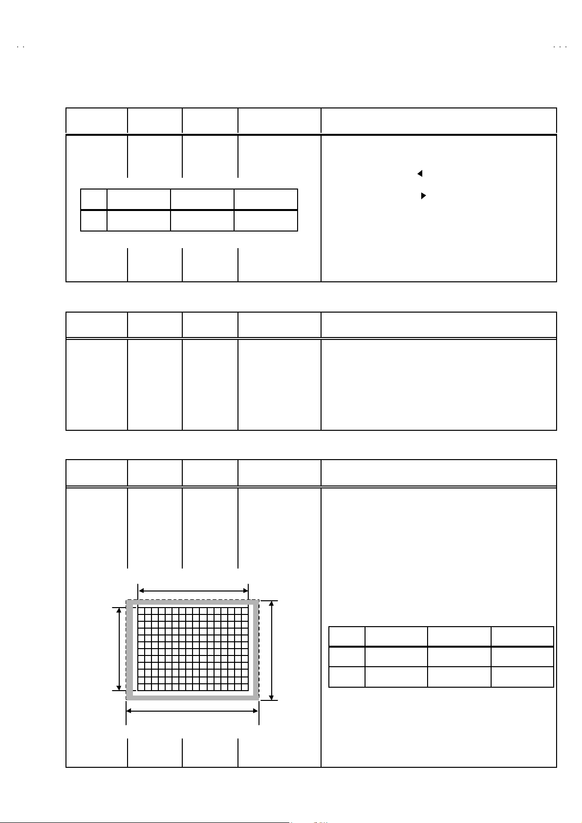
PIP DIS PLA Y
POSITION
adj ust ment
(AV-27F 80 3/S)
Signal
generator
PI P scre en
-128~+127
-128~+127
-128~+127
-128~+127
00
00
00
00
PIP1 1:L POS I.
PIP1 2:R POS I.
PIP1 3:UPR POS I.
PIP1 4:LW R POSI.
X1
(UPPER POSI.)
* Main pictur e’s V. HE IGHT, V . PO SI, H. SIZE , H. POSI. Shoul d
be fi nis he d.
* Set t he VIDEO STATU S to STAND ARD.
1. Recei ve a blac k - an d- w hi te sign al ( col or of f)
2. Enter the SERV ICE MENU .
3. Sel ect th e 5:PI P(PIP) fr om SERVIC E MEN U.
4. Set t he initial setting value of the PIP13:UPR P OSI. with the
( / ) key of the remote control unit.
5. Adj ust th e PI P1 3: UPR POSI . so th at he posi ti o n of t he PIP
screen edg e of upp er will be at X1 as sh o wn.
6. Adjus t the cor r es p on di ng mod es o f PI P14, PIP11, PIP 12 wi t h
the s ame st eps as 3~5 abo ve.
Item
PIP1 3 UPR POSI 0~127 12 X1 80
No.
Setting
item
Vari able
range
setting
value
Setting position
POSI. (%)
PIP1 4 LW R POSI
PIP1 1 L. POSI
PIP1 2 R. POSI
0~127
0~255
0~255
Y1
(LEFT POSI.)
X2
(LOWE R PO SI. )
Y2
(RIGHT POSI.)
No. 52005
11 X2 80
22 Y1 80
15 Y2 80
25
Page 26
A
V-27F703
A
A
V-27F713
V-27F803
ADJUS TMENT OF VIDEO / CHROMA CIRCUIT
Item
WHITE
BALANCE
(Low Light)
adjus tment
Measuring
instrume nt
Signal
generator
Test point Ad justment part Description
[LOW LIGHT]
BRIGHT
** * *** * **
***
S01:B RIG HT
S11:R CUTOFF
S12:G CUTOFF
S13:B CUTOFF
SCREEN VR
[ in HVT]
1. Recei ve th e blac k an d wh it e signal ( col or o ff ) .
2. Se lec t t he LOW LIGHT mode from the SERVICE MENU.
3. Confirm the initial setting value of R CUTOFF, G CUTOFF,
B CUT OFF and BRI G HT .
0. Display a sing le ho rizo nta l lin e by p r es sing t he ①①①① key of the
remote control unit.
5. Tur n the scr een VR a l l the way t o t he l eft.
6. Turn th e scr een V R g ra du al ly to the righ t from th e left u nti l
eith er o ne of the r ed, blu e o r g reen co lors ap pears f aintly.
7. Adju st th e two col or s which d id no t a ppe ar u ntil th e sing le
h oriz o nt al lin e t hat is disp la yed bec omes white usin g th e ④④④④
⑨⑨⑨⑨
to
keys of th e r em ot e contr o l un it.
8. Tur n th e scr ee n VR u ntil the si ng le h or i zon tal li n e i s displ a y ed
fain tly.
9. Pr es s the
10 . Ad jus t the BR IG HT lev el to b ecome th e bl ac k c omp on en t
shines white slightly.
11 . Conf ir m th at wh eth er the color i ng redie nt of R, G, o r B is visi bl e
to th e bl ac k c o mp one nt, which shine s whi te sl ig htl y
12 . When th e col o r in gr ed ient can be s een , t wo c olors o ther tha n a
visible color are adjusted, and it is made to look white.
13. Return the va lue of BRIGHT to initi al s etting value.
②②②②
key to cancel the single horizontal line mode.
[H.LINE SCREEN ]
REMOTE CONTROL UNIT
H.LINE ON EXITH.L IN E OFF
1
R C UTOF F B C UTOF FG CUTOFF
4
R C UTOF F B C UTOF FG CUTOFF
7
2
5
8
●
③③③③
The
EX IT key is the cancel key for the WHIT E BALANCE.
No. Setting item
S11 R CUT OFF
Variabl e
range
0~255
Initial set ting
value
30
3
S12 G CUT OFF 0~255 30
6
S13 B CUT OFF 0~255 30
S01 BRIG HT 0~127 64
9
26
No.52005
Page 27

A
V-27F70
3
A
3
A
3
V-27F71
V-27F80
Item
WHITE
BALANCE
(High Light)
adjus tment
Measuring
instrume nt
Signal
generator
*** ***
[WHITE SCREEN]
REMOTE CONTROL UNIT
H.LINE ON EXITH.L IN E OFF
1
R D RI VE
Test point Ad justment part Description
2
3
B D RI VE
S14:R DRIVE
S15:B DRI VE
1. Recei ve th e blac k- a nd -w hit e sign al ( col o r off ).
2. Se lec t t he HIGH LIGHT mode in the SERVICE MENU.
3. Se t the ini ti a l se tting val u e of R DR I V E an d B DRIVE with the
④④④④ , ⑥⑥⑥⑥, ⑦⑦⑦⑦and ⑨⑨⑨⑨ keys of th e r em ot e contr o l uni t.
4. Ad just t he s cr ee n u nti l it b ec om es wh ite usi ng the ④④④④ , ⑥⑥⑥⑥, ⑦⑦⑦⑦
an d ⑨⑨⑨⑨ keys of th e r em ot e contr o l uni t.
●The ③③③③ EX IT key is the cancel key for the WHIT E BALANCE.
No. Setting item
S14 R DRI VE 0~127 64
S15 B DRIVE 0~127 64
Variabl e
range
Initial set ting
value
PIP W HI TE
BALANCE
(High Light)
adjus tment
(AV-27 F8 03 O NL Y)
4
R DRIVE B DRIVE
7
Signal
generator
5
8
6
9
PIP08:R DRIVE
PIP10:B DRIVE
1. Recei ve th e blac k- a nd -w hit e sign al ( col o r off ).
2. Se lec t t he PI P08: R DR IVE, PIP10 :B DR IVE, of t he 5.PIP( PIP)
SERVICE MENU.
3. Set th e corresp onding initial sett in g va lues with th e
FUNCTION ( / ) key of t he remote contr ol un it.
4. Ad jus t t he PIP08:R DRIV E, PI P10:B DRIVE un ti l th e s cr een
becomes white.
No. Setting item
PIP 08 R DRI VE 0~255 63
PIP10 B DRIVE 0~255 65
Variabl e
range
Initial set ting
value
No.52005
27
Page 28

A
V-27F703
A
A
(A)
g
(-)
V-27F713
V-27F803
Item
SUB BRI GHT
adjus tment
No. Setting item
S01 BRIG HT
SUB
CONT RAST
adjus tment
No. Setting item
S02 PIC TU RE 0~127 60
SUB COLOR
adjus tment
No. Setting item Variable
S03 COLOR 0~127 50
Measuring
instrume nt
Signal
generator
Remote
control unit
Test point Ad justment part Description
Variabl e
range
0~127 64
Variabl e
range
range
S01:BRI GHT
Initial set ting
value
S02:PICTURE
Initial set ting
value
S03:C OL OR
Initial set ting
value
1. Receive the broadcast and set the STANDARD mode.
2. Enter the SERVICE ME NU.
3. Select S01:BRIGHT of the V/C(S) m ode.
4. Se t the init i al s ettin g value of the S0 1. BRIGH T with the
FUNCTION / key.
5. If the brightness is not the best with the initial s etting value,
make fi ne a djustmen t of th e S01. BRIGHT until you get the
op ti mu m bright ness .
1. Receive the broadcast and set the STANDARD mode.
2. Enter the SERVICE ME NU.
3. Select S02:PICTURE of the V/C (S) m ode.
4. Se t the ini ti a l se tting val ue of the S02:PICTURE with the
FUNCTION / key.
5. If the contrast is not the best with the initial setting value, make
fin e adjustm ent of the S02:PICTURE u ntil you get the optim um
contrast.
[ Method of adjustment without measuring instr ument ]
1. Recei ve th e b road c ast.
2. Enter the SERVICE ME NU.
3. Select S03:COLOR of the V/C( S) mod e.
4. Se t the in it ial s etti ng value of the S0 3: COLOR with the
FUNCTION / key.
5. If the c ol or is no t th e b est with t he Initia l s etti n g value, m a k e
fin e adj us tm ent of th e S0 3:COLOR unt i l yo u g et the op ti mu m
color.
generator
Oscilloscope
Remote
control unit
Y
W
TP-B
TP-E(#### )
[CRT
SOCKET
PWB]
G
Cy
S03:C OL OR
R
M
0V
(+)
[ Method of adjustment using measuring instrum ent ]Signal
1. Inp ut th e ful l fi el d c olor b ar si gn al ( 7 5% whi t e).
2. Enter the SERVICE ME NU.
3. Set th e RFAFC to OFF.
4. Select S03:COLOR of the V/C( S) mod e.
5. Set the initial setting value of the S0 3:COLOR with the
FUNCTION / key.
6. Con nect th e osc illosc ope be tw ee n TP-B and TP-E.
7. Ad ju st COL OR a nd br ing th e value of (A) in the illustration to
th e vo lt ag e shown in the t abl e be ll o w.
8. Reset the RFAF C set ti ng positio n from OFF to ON .
Models
AV-27F703
AV-27F713
AV-27F803
W-B
/S
/S
/S
[A]Voltage
+13V
B
28
No.52005
Page 29

A
V-27F70
3
A
3
A
3
y
g
g
V-27F71
V-27F80
Item
adjus tment
Measuring
instrume nt
Signal
generator
Remote
control unit
generator
Oscilloscope
Remote
control unit
Test point Ad justment part Description
[ Method of adjustment without measuring instr ument ]SUB TINT
1. Recei ve th e b road c ast.
2. Enter the SERVICE ME NU.
3. Select S04:T INT of th e V /C(S) mod e.
4. Se t t he ini t ial se tti ng va l ue of t he S04:TIN T with the
FUNCTION / key.
5. If the tint i s n ot the bes t w ith the ini tia l set ting v al u e, m ak e fi ne
ad justmen t of the S0 4:TIN T until you get t he optimum ti nt.
No. Setting item
S04 TINT
[ Method of adjustment using measuring instrum ent ]Signal
1. Inp ut th e ful l fi el d c olor b ar si gn al ( 7 5% whi t e).
2. Enter the SERVICE ME NU.
3. Set th e RFAFC to OFF.
4. Select S04:TINT of th e V/C( S) mod e.
5. Set th e i ni t ia l se tti ng val u e of th e S0 4:TINT with the
FUNCTION / key.
6. Con nect th e osc illosc ope be tw ee n TP-B and TP-E.
7. Ad ju st TINT and br ing th e valu e of (B) i n the illu str ation to the
voltage shown in the table bellow.
8. Reset the RFAFC set ting pos itio n f rom OF F to ON.
Variabl e
range
0~127
TP-B
TP-E(#### )
[CRT
SOCKET
PWB]
S04:T INT
S04:T INT
Initial set ting
value
68
W
Y
G
C
R
AV-27F703
AV-27F713
(B)
B
(-)
0V
(+)
AV-27F803
W-M
[B]Voltage
/S
/S
/S
+26V
M
No.52005
29
Page 30

A
V-27F703
A
A
V-27F713
V-27F803
ADJUS TMENT OF MTS CIRCU IT
Item
MTS IN PUT
LEVE L
Ad j ust men t
Measuring
instrume nt
Sopho meter AUDIO
Test point Ad justment part Description
OUT R pin
A01 :IN LE VEL 1. Rec ei ve the cr os s- hatc h sign al (c ros s-h atch / 400H z)
2. Enter the SERVICE ME NU.
3. Se lec t t he A 01: IN L EV EL of the 3:SOUND(A) MODE.
4. Verif y that th e A01:IN LEVEL is set at its initial setting value.
5. Connect th e sopho m ete r t o AUDIO OUT R pi n .
6. Ad just th e MTS i npu t l eve l to 5 00 mV(r ms) b y A01 : IN LEVEL
with remote control unit.
7. Press the EXIT key to return to the SERVICE MENU screen.
MTS
SE PARATIO N
adjust ment
TV audio
mult iplex
signal
generator
Oscilloscope
R OUT
L OUT
[AUDIO OUT]
A02 : LOW SE P.
A03:HI SEP.
No. Setting item
A01 IN LEVEL 0~15 01 0
1. Inp ut th e ster e o L sign al (300 Hz) fr om the TV au dio multiple x
si gn al g ener ator to th e ant enna ter m in al.
2. Connect an oscilloscope to R OUT pin of th e A UDIO OUT, a nd
disp l ay on e c ycle port ion of t he 300H z s i g nal .
3. Enter the SERVICE ME NU.
4. Se lec t t he A 02:L OW SE P. of the 3:SOUND(A) mode.
5. Set th e i ni ti al s etti ng valu e of t he A02:LOW SEP. wit h the
FUNCTION ( / ) ke y.
6. Ad jus t t he A02:LOW SE P. so that the stroke element of the
300Hz signal will become minimum.
7. Change the connection of the oscilloscope to L O UT pin of the
AUDIO O UT , and en lar ge th e volt age axis.
8. C ha nge th e s ign al to 3 kH z, an d s imil ar l y adjust th e
A03:HI SEP.
9. Press the EXIT key to return to the SERVICE MENU screen.
Variabl e
range
Initial set ting
value
Setting item
L- Chann el
signal wave for m
1 c ycle
30
R-C hannel
crosstalk por ti on
Mi n i m u m
No.52005
No .
A02 LOW SEP.
A03 HI SE P.
Variabl e
range
0~63
0~63
Initial set ting
value
03 2
03 2
Page 31

A
3
A
3
A
3
HOW TO CHECK THE HIGH VOLTAGE HOLD DOWN CIRCUIT
CO
S1Q53
53 5
Q532Q95
95 0
ONO
93 5D525D53
1. HIGH VOLTAGE HOLD DOWN CIRCUIT
After repairing the high voltage hold down circuit shown in Fig. 1.
Thi s ci r cuit sh all b e ch ecked to op er at e co rrect ly.
2. CHECKING OF THE HIGH VOLTAGE HOLD DOWN CIRCUIT
(1) Turn the power switch to on.
(2) As s h ow n i n Fig. 1, set t he r esistor b etwee n S1 c on nect or 2 an d 3 .
(3) Make sure t hat th e scr ee n pic ture disappe ar s.
(4) Temporarily unplug the power plug.
(5) Remove the resistor replac ed S1 connec tor 2 an d 3 .
(6) Ag ai n pl ug the p ow er plu g , make s u re th at t he no rm al pi ctur e is displ a yed on th e scr ee n.
RESISTOR
Ω±
Ω±
ΩΩΩΩ
Ω±Ω±
V-27F70
V-27F71
V-27F80
1
R
NNECTOR
FF
D
1
R
4
Fig. 1
4
No.52005
31
Page 32

A
V-27F703
A
A
V-27F713
V-27F803
REPLACEMENT OF CHIP COMPONENT
!
CAUT IONS
1. Avoid heating for more than 3 seconds.
2. Do not ru b t he el ect ro des and t he resi st p ar ts of the p att ern.
3. W hen r em oving a c hi p par t, mel t th e s older adequ ately .
4. Do not reuse a ch ip p ar t afte r re mo vi ng it .
! SOLDERING IRON
1. Use a hig h ins ulati o n solder ing i r on with a t hin po in ted e nd of it .
2. A 3 0 w s older ing i r on is r ec ommended for easily r em ovi ng par ts.
! REPLACEMENT STEPS
1. How to remove Chip parts
#### Resi st o rs, capacitor s , et c
(1) As s h own in t he f igur e, pu sh th e pa rt wi th tw ee zer s and
alte rn at ely m el t the s ol de r at each en d.
(2) Sh if t w i th tweez e rs and r emo ve th e ch i p p ar t.
#### T ran s istors, d io des , va ria bl e r esistors, et c
(1) Ap pl y e xt ra s o ld er to each le ad .
SOLDE R SO LD ER
2. How to install Chip parts
####
Resi st ors, ca pacitors , et c
(1) Apply sold er to the patt ern as ind icated in the fi g ure.
(2) Gr asp t he c h i p p art with twee zer s and pl ac e it on the s older.
The n hea t and me lt th e so lder a t b oth ends of t he chip part.
#### Tran s istors, d io des , va ria bl e r esistors, et c
(1) Apply sold er to the patt ern as ind icated in the fi g ure.
(2) Grasp the c h ip p art wit h t we ez e rs and p lace it on th e so l der .
(3) First s older lead A as indicated i n t he figu re.
A
(2) As s h own in t he f igur e, pu sh th e pa rt wi th tw ee zer s and
alte rn at ely m el t th e sol d er at each le ad . S hi ft an d r em ove t he
chip part.
(4) The n solder le ads B and C.
Note : A fte r re moving t he part , remove r emaining solder fr o m the
pattern.
32
No.52005
C
A
C
B
B
Page 33

SCHEMATIC DIAGRAMS
COLOR TELEVISION
AV-27F703
AV-27F713
AV-27F803
AV-27F703/S
AV-27F713/S
AV-27F803/S
CD-ROM No.SML200207
BASIC CHASSIS
GJ
TV TV
RM-C326G
[ ]
RM-C326
AV-27F703
AV-27F713
[RM-C325G]
AV-27F803
CONTENTS
NOTE ON USING CIRCUIT DIAGRAMS
SEMICONDUCTOR SHAPES
BLOCK DIAGRAM
CIRCUIT DIAGRAMS
PATTERN DIAGRAMS
CHANNEL CHART
COPYRIGHT 2002 VICTOR COMPANY OF JAPAN, LTD.
2-1
2-2
2-3
2-7
2-21
2-29
No.52005
Jun. 2002
Page 34

Page 35

AV-27F703
STA NDARD CIRCUIT DIAGRAM
NOTE ON USING CIRCUIT DIAGRAMS
1.SAFETY
The components identified by the symbol and shading are
critical for safety. For continued safety replace safety critical
components only with manu factures recommended parts.
2.SPECIFIED VOLTAGE AND WAVEFORM VALUES
The voltage and waveform values have been measured under the
following conditions.
(1)Input signal : Colour bar signal
(2)Setting positions of
each knob/button and
variable resistor
(3)Internal resistance of tester
:DC 20k
/V
(4)Oscilloscope sweeping time
:H
20µS/div
:V
5mS/div
:Others
Sweeping time is
specified
(5)Voltage values
:All DC voltage values
Since the vol tage values o f signal cir cuit vary to some extent
according to adjustments, use them as reference values.
3.INDICATION OF PARTS SYMBOL [EXAMPLE]
In the PW board
:R1209
R209
4.INDICATIONS ON THE CIRCUIT DIAGRAM
(1)Resistors
Resistance value
No unit :[
]
K
:[K
]
M
Rated allowable power
No indication :1/ 1 6 [W]
Others :As specified
Type
No indication
:Carbon resistor
OMR
:Oxid e metal film res istor
MFR
:Metal film resistor
MPR
:Metal plate resistor
UNFR
:Uninflammable resistor
FR
:Fusible resistor
Composition resi stor 1/2 [W] is spe cified as 1/ 2S or Comp.
(2)Capacitors
: Original setting position
when shipped
5.NOTE FOR RE PAIRI N G S ERVI CE
This mod el's power cir cuit is pa rtly diffe rent in the GND. The
difference of the GND is shown by the LIVE : ( ) side GND and the
ISOLATED(NEUTRAL) : ( ) side GND.Therefore, care must be
taken for the following points.
(1)Do not touch the LIVE sid e GND or the LIVE side GND and the
ISOLATED(NEUTRAL) side GND simultaneously. If the above
caution is not respected, an electric shock may be caused.
Therefore, make sure that the power cord is surely removed from
the receptacle when, for example, the chassis is pulled out.
(2)Do not short between the LIVE side GND an d ISOLATED(NEUTRAL)
side GND or never measure with a measuring apparatus measure
with a measuring apparatus ( oscilloscope, etc.) the LIVE side GND
and ISOLATED(NEUTRAL) side GND at the same time.
If the above precaution is not respected , a fuse or any parts will be broken.
Since the circuit diagram is a standard one, the ci rcuit an d
circuit constants may be subject to change for improvement
without any n otice.
NOTE
Due improvement in performance, some part numbers show
in th e ci rcui t diag ram may not ag ree wi th th ose ind ica ted in
the part list.
When ordering parts, pl ease use the numbers t hat appear
in the Parts List.
Type
MM
:Metalized mylar capacitor
PP
:Polypropylene capacitor
MPP
:Metalized polypropylene capacitor
MF
:Metalized film capacit or
TF
:Thin film capacitor
BP
:Bipolar electrolytic capacitor
TAN
:Tantalum ca pacitor
(3)Coils
No unit
:[
µ
H]
Others
:As specified
(4)Power Supp ly
:B1
:9V
:5V
Respective voltage values are indicated
(5)Test point
:T est point
:Only test point display
(6)Conn ecting method
:Connector
:Wrapp ing or sold eri ng
:Receptacle
(7)Ground symbol
:LIVE side ground
:ISOLATED(NEUTRAL) side ground
:EARTH ground
:DIGITAL ground
:[M ]
Capacitance value
1 or higher :[pF]
less than 1
:[µF]
Withstand voltage
No indication :DC50[V]
Others :DC withstand voltage [V]
AC indicated
:AC withstand voltage [V]
Electrolytic Capacitors
47/50[Example]:Capacitance value [µF]/withstand voltage[V]
No indication
:Ceramic capacitor
:B2 (12V)
AV-27F703/S,AV-27F713/S,AV-27F803
/S
AV-27F713
AV-27F803
Jun. 2002 No. 52005
Page 36

AV-27F703
STA NDARD CIRCUIT DIAGRAM
NOTE ON USING CIRCUIT DIAGRAMS
1.SAFETY
The components identified by the symbol and shading are
critical for safety. For continued safety replace safety critical
components only with manu factures recommended parts.
2.SPECIFIED VOLTAGE AND WAVEFORM VALUES
The voltage and waveform values have been measured under the
following conditions.
(1)Input signal : Colour bar signal
(2)Setting positions of
each knob/button and
variable resistor
(3)Internal resistance of tester
:DC 20k
/V
(4)Oscilloscope sweeping time
:H
20µS/div
:V
5mS/div
:Others
Sweeping time is
specified
(5)Voltage values
:All DC voltage values
Since the vol tage values o f signal cir cuit vary to some extent
according to adjustments, use them as reference values.
3.INDICATION OF PARTS SYMBOL [EXAMPLE]
In the PW board
:R1209
R209
4.INDICATIONS ON THE CIRCUIT DIAGRAM
(1)Resistors
Resistance value
No unit :[
]
K
:[K
]
M
Rated allowable power
No indication :1/ 1 6 [W]
Others :As specified
Type
No indication
:Carbon resistor
OMR
:Oxid e metal film res istor
MFR
:Metal film resistor
MPR
:Metal plate resistor
UNFR
:Uninflammable resistor
FR
:Fusible resistor
Composition resi stor 1/2 [W] is spe cified as 1/ 2S or Comp.
(2)Capacitors
: Original setting position
when shipped
5.NOTE FOR RE PAIRI N G S ERVI CE
This mod el's power cir cuit is pa rtly diffe rent in the GND. The
difference of the GND is shown by the LIVE : ( ) side GND and the
ISOLATED(NEUTRAL) : ( ) side GND.Therefore, care must be
taken for the following points.
(1)Do not touch the LIVE sid e GND or the LIVE side GND and the
ISOLATED(NEUTRAL) side GND simultaneously. If the above
caution is not respected, an electric shock may be caused.
Therefore, make sure that the power cord is surely removed from
the receptacle when, for example, the chassis is pulled out.
(2)Do not short between the LIVE side GND an d ISOLATED(NEUTRAL)
side GND or never measure with a measuring apparatus measure
with a measuring apparatus ( oscilloscope, etc.) the LIVE side GND
and ISOLATED(NEUTRAL) side GND at the same time.
If the above precaution is not respected , a fuse or any parts will be broken.
Since the circuit diagram is a standard one, the ci rcuit an d
circuit constants may be subject to change for improvement
without any n otice.
NOTE
Due improvement in performance, some part numbers show
in th e ci rcui t diag ram may not ag ree wi th th ose ind ica ted in
the part list.
When ordering parts, pl ease use the numbers t hat appear
in the Parts List.
Type
MM
:Metalized mylar capacitor
PP
:Polypropylene capacitor
MPP
:Metalized polypropylene capacitor
MF
:Metalized film capacit or
TF
:Thin film capacitor
BP
:Bipolar electrolytic capacitor
TAN
:Tantalum ca pacitor
(3)Coils
No unit
:[
µ
H]
Others
:As specified
(4)Power Supp ly
:B1
:9V
:5V
Respective voltage values are indicated
(5)Test point
:T est point
:Only test point display
(6)Conn ecting method
:Connector
:Wrapp ing or sold eri ng
:Receptacle
(7)Ground symbol
:LIVE side ground
:ISOLATED(NEUTRAL) side ground
:EARTH ground
:DIGITAL ground
:[M ]
Capacitance value
1 or higher :[pF]
less than 1
:[µF]
Withstand voltage
No indication :DC50[V]
Others :DC withstand voltage [V]
AC indicated
:AC withstand voltage [V]
Electrolytic Capacitors
47/50[Example]:Capacitance value [µF]/withstand voltage[V]
No indication
:Ceramic capacitor
:B2 (12V)
AV-27F703/S,AV-27F713/S,AV-27F803
/S
AV-27F713
AV-27F803
CONTENTS
SEMICONDUCTOR SHAPES
BLOCK DIAGRA M
CIRCUIT DIAGRAMS
MAIN P W B CIRCUIT DIAGRAM
CRT SOCKET PWB CIRCUIT DIAG RAM
AV SEL PWB CIRCUIT DIAG RAM
FRONT CONTROL PWB CIRCUIT DIAG RAM
LED & POWER SW PWB CIRCUIT DIAGRAM
PIP PWB CIRCUIT DIAGRAM
P ATTERN DIAGRAMS
MAIN PWB PATTERN
AV SEL
PIP PW B PATTERN
CRT SOCKET PWB PATTERN
FRONT CONTROL PWB PATTERN
LED & POWER SW PWB PATTERN
CHANNEL CHART
CHANNEL CHART
SEMICONDUCTOR SHAPES
TRANSISTOR
BOTTOM VIE W
IC
CHIP IC
2-2
PWB PATTERN
(US)
(CA)
ECB
IN OUTE
BCE
(G)(D)(S)
E
C
B
B O TT OM VI EW F R O NT VIEW TO P VI EW
OUT
E
IN
N
N
N
1
N
FRONT VIEW
ECB
ECB
1 N
TO P VI EW
1
N
No.52005
1 N
TO P VI EW
CHIP TR
1
C
BE
N
2-2
2-3
2-7
2-11
2-13
2-17
2-18
2-19
2-21
2-23
2-25
2-27
2-28
2-28
2-29
2-30
Page 37

Page 38

2
2
2
BLOCK DIAGRAM [AV-27F703,AV-27F713]
TU001
VIDEO
INPUT 1
PC921
VOLTAGE
FEED BACK
IC921
ERROR
AMP
D901
IC911
POWER IC
B1
IC201
MICOM/V/C/DEF
IF
Y/C
V1
L1
R1
V2
L2
R2
L
R
VIDEO
INPUT 2
AUDIO
OUT
COMPU
LINK EX
T921
SW.
TRANSF.
MAIN PWB
IC101
IF DET
TUNER
IC5501
IC5151
IC5001
IC5201
BBE
MTSIC
3L DIGI
AV SW
AV SEL PWB
MON L/R
Y/C
V1
V2
V3
L1/R1
L2/R2
L3/R3
V
Y
Y
C
C
Y/C OUT
L/R OUT
L/R
L/R
VTV
MPX
MPX
VTV
Y/C OUT
Y
R-Y
B-Y
R/G/B
COMP LINK
H
V
LF901
COMPO-
-NENT
INPUT 2
Y
Pb
Pr
Y/Pb/Pr
S VM
AV-
AV-27F703
AV-27F713
AV-27F803
AV-
AV-
No.52005
2-3 2-4
Page 39

27F703
27F713
27F803
AV-27F703
AV-27F713
AV-27F803
FRONT
CONTROL
PWB
RM LED SW
SW
V3
L3
R3
VIDEO
INPUT 3
IC5151
Y
R-Y
B-Y
01
/V/C/DEF
BBE
S VM
L/R
R/G/B
IC702
MEMORY
IC621
AUDIO AMP
L , R
L/R
L R
LED& POWER SW PWB
R/G/B
Q3351
Q3353
RGB DRV
VM AMP
CRT SOCKET PWB
L
R
SP L
SP R
CRT
VM COIL
H
MAIN PWB
2-3 2-4
Q511
H.OUT
IC421
VERT OUT
B1
T502
HVT
FOCUS
SCREEN
DY01
(ITC)
H
V
No.52005
Page 40

BLOCK DIAGRAM [AV-27F803]
E
P
Y/C
VIDEO
INPUT 1
VIDEO
INPUT 2
V1
L1
R1
V2
L2
R2
Y/C
V1
L1/R1
V2
L2/R2
L4/R4
V3
L3/R3
IC5501
AV SW
Y
C
Y/C OUT
L/R OUT
AV-27F703
AV-27F713
AV-27F803
V
IC5301
V
REG.
Y
C
3D Y/C SE
AV-27F
AV-27F
AV-27F
3D Y/C
SEP
PWB
VIDEO
INPUT 4
AUDIO
OUT
COMPO-
-NENT
INPUT 2
COMPO-
-NENT
INPUT 4
L4
R4
AV SEL PWB
L
R
Y
Pb
Pr
Y
Pb
Pr
TU001
TUNER
IF
IC602
SW
VTV
VTV
IC101
IF DET
Y/Pb/Pr
MON L/R
MPX
MPX
IC5001
MTSIC
Y/Pb/Pr
Y/C OUT
L/R
IC601
IC5151
SW
Y
R-Y
B-Y
IC201
MICOM/V/C/DEF
BBE
PIP
R/G/B
L/R
R/G/B
S VM
COMPU
LINK EX
LF901
D901
No.52005
IC911
POWER IC
COMP LINK
T921
SW.
TRANSF.
PC921
VOLTAGE
FEED BACK
IC921
ERROR
AMP
B1
V
H
V
MAIN PWB
2-5 2-6
Page 41

F703
F713
F803
Y
AV-27F703
AV-27F713
AV-27F803
3D Y/C
SEP
PIP PWB
TU4001
TUNER
IF
FRONT
CONTROL
PWB
V3
L3
R3
VIDEO
INPUT 3
1
Y
Y
C
3D Y/C SEP
PWB
IC5151
BBE
PIP
R/G/B
S VM
L/R
R/G/B
IC4101
IF DET
V PIP
IC4301
PIP
CONTROLER
PIP
R/G/B
IC621
AUDIO AMP
L , R
L R
SW
RM LED SW
LED& POWER SW PWB
R/G/B
Q3351
Q3353
RGB DRV
VM AMP
CRT SOCKET PWB
L
SP L
CRT
VM COIL
1
/C/DEF
MAIN PWB
2-5 2-6
MEMORY
Q511
H.OUT
IC421
VERT OUT
IC702
B1
T502
HVT
L/R
FOCUS
SCREEN
R
No.52005
SP R
DY01
(ITC)
H
V
Page 42

2
2
2
CIRCUIT DIAGRAMS MAIN PWB CIRCUIT DIAGRAMS
6.1V
6.1V
6.1V
6.1V
6.1V
6.1V
0V
0V
0V
9V
4.8V
0V
4.8V
2.9V
9V
4.5V
3.8V
1V
4.7V
3.9V
4.2V
4.7V
31.3V
0V
1V
9V
1.8V
5.5V
2.3V
3.2V
0V
0V
0V
1.4V
1.4V
4.8V
2.5V
5.8V
2V
2.6V
2.1V
3.3V
2.1V
9V
3.9V
3.9V
4.8V
2V
3.4V
1.5V
1.6V
0.9V
2.3V 2V
2.1V 5.1V 2V
2.2V
2.1V
0V
0V
3.2V 4.1V
3.4V
0V
2.1V
5.9V
0.1V
2.5V 3.8V
1.6V
2.5V
2.8V
4.7V
1.8V 1.9V
1
2
IC201
14
18
28
39
40
41
5
1.8
0.9
3.5
3
3
4.6V
4.5V
8.9V
6.1V 4.5V
4.5V
4.5V
6.1V
3.1V
4.6V
6.1V
3.1V
3.1V
26
0.3
CRT SOCKET P
AV SW PWB
PIP PWB
!
COMPONENT
INPUT 4
COMPONENT
INPUT 2
4
.7
k
R
3
1
8
1k
R319
.1
C222
CN002
1
2
0
k
R
2
9
2
5.6k
R215
10
/16
N
C211
OPEN
R291
1SS133-T2
D307
C402
OPEN
Y601
OPENY602
OPENY603
OPEN
Y604
OPEN
Y605
OPEN
Y606
M
T
Z
J
3
.3
B
-T
2
D
3
5
4
220k
R293
.01
C237
.1
C609
.1
C610
.1
C611
10
/50
C286
*
R610
1
5
0
k
R
2
8
9
1
0
0
R
2
8
7
1
0
0
R
2
8
1
.01
C241
.0
1
C
3
5
4
C203
.0
1
C
2
4
4
1
0
0
R
3
0
4
1
0
0
R
3
0
5
R
3
0
6
10k
R359
100k
R227
22k
R201
*
R611
*
R612
10
/50
C221
2.2/50
C242
1
/5
0
C
2
0
2
1
0
0
/1
6
C
2
4
3
22
L241
1SS133-T2
D353
*
C604
*
C605
.*
C606
TM
M
IC201
.4
7
C
2
8
1
OPEN
Y607
OPENY608
OPEN
Y609
OPEN
Y610
47/25
C603
*
IC601
75
R601
75
R602
NQR0169-001X
LC601
NQR0169-001X
LC602
75
R603
47/25
C601
47/25
C602
NQR0169-001X
LC603
.0082
C285
O
P
E
N
R
2
0
2
*
C654
OPEN
R607
OPEN
R608
OPEN
R609
MTZJ9.1C-T2
D603
MTZJ9.1C-T2
D602
100
/16
C287
MTZJ9.1C-T2
D601
*
C607
*
C608
1SS133-T2
D306
.01
C288
1SS133-T2
D305
1SS133-T2
D310
1SS133-T2
D309
1SS133-T2
D308
0
R222
*
R615
*
R614
*
R613
CH
OPEN
C214
10p
C
H
C212
OPEN
R213
OPEN
R214
2.7k
R212
5.6k
R216
2SD601A/QR/-X
Q211
1k
R217
CH
OPEN
C213
OPEN
R219
OPEN
Q212
OPEN
Q213
OPEN
R218
OPEN
R221
OPEN
R220
CH
OPEN
C218
CH
OPEN
C219
OPEN
Y611
OPENY612
R651
R652
R653
.1
C302
5
6
0
R
2
9
0
4
7
0
R
2
8
8
CN001
*
C653
*
C652
*
C655
QNN0349-002
J601
2SB709A/QR/-X
Q131
QQR0907-001
CW TRANSF
T111
1
0
0
R
1
1
5
4.7
QQL244K-4R7Z
L113
O
P
E
N
L
1
0
2
1k
R164
3
.3
k
R
1
6
1
1
0
/5
0
C
1
6
1
.0
1
C
1
2
4
.0
1
C
1
1
4
.0
1
C
1
1
3
O
P
E
N
R
1
2
0
OPEN
R121
2
2
0
k
R
1
1
1
QAX0349-001
CF001
O
P
E
N
R
1
1
2
CH
OPEN
C132
4.7
/50
C001
O
P
E
N
C
1
2
2
10
/50
C003
OPEN
C103
56
L001
1
0
0
R
1
1
3
0
R002
0
R162
100
R004
0
R005
100
R003
OPEN
R001
OPEN
R006
OPEN
C010
OPEN
C011
2
2
k
R
1
1
8
OPEN
C162
2
7
k
R
1
1
7
330
R132
O
P
E
N
R
1
1
4
560
R134
.2
2
T
F
C
1
1
6
5.6k
R101
82
R008
1.8k
R102
1
0
k
R
1
7
1
2
2
k
R
1
6
3
100
R1/2
R103
47/25
C006
18
R104
.01
C166
.4
7
/5
0
C
1
2
0
820
R133
.01
C131
47
/25
C106
4
7
/2
5
C
1
1
7
.01
C107
.22 QQLZ014-R22L101
15
L131
680p
CH
C119
1k
R131
27
R105
*
C614
6
8
R
1
1
6
*
IC602
*
R604
QAX0639-001Z
4.5MHz TRAP
CF131
.0
1
C
1
1
8
.01C101
2SC5083/L-P/-T
Q101
.01
C102
.01
C104
*
R605
QAX0723-001
SF101
47p
C16347p
C164
22
QQL244K-220Z
L161
QAX0642-001Z
CF161
22k
R165
10k
R166100
R168
1k
R167
560
R169
.01
C165
2SB709A/QR/-X
Q161
*
LC604
1000/16
C004
*
LC605
*
R606
*
C612
OPEN
L114
OPEN
R119
OPEN
C121
.01
C105
1k
R135
QAU0272-001
QAU0274-001
TUNERTU001
M52342SP
IC101
*
C613
*
LC606
*
R618
*
R617
*
R616
*
D606
*
D605
*
D604
*
C615
*
C616
O
P
E
N
R
3
0
1
*
J602
O
P
E
N
R
3
0
2
CN0E4
OPEN
C651
OPEN
Q261
OPEN
R654
OPEN
D651
OPEN
D652
*
Y201
C
2
8
4
*
D
6
5
3
*
D654
*
R655
UN2212-X
Q001
6.8k
R009
R294
R295
C656
C657
C658
OPEN
C355
C
O
M
_
Y
COMP
BSR_BY2
V
s
a
w
V
o
u
t
E
W
_
o
u
t
X
ra
y
Y
s
C
b
_
in
p
u
t
Y
_
in
p
u
t
C
r_
in
p
u
t
D
v
c
c
_
3
.3
V
V
in
3
/C
in
E
H
T
_
in
V
in
2
/Y
Y
C
D
_
G
N
D
V
in
1
A
B
C
L
M
o
n
ito
r
B
la
c
k
_
D
e
t
S
V
M
_
o
u
t
A
P
L
_
F
il
A
P
C
_
F
il
3
.5
8
M
H
z
Y
C
_
V
c
c
_
5
V
R
_
o
u
t
G
_
o
u
t
R
A_GND
AMP
AMP
SWITCH
GND
GND
GND
GND
GND
HP
VP
5V
5V
5V_GND
5V_GND
YS_PiP
PB_PiP
Y_PiP
PR_PiP
V_PiP
VPiP_GND
SDA0
SCL0
9V_GND
9V_GND
9V
9V
30V
AFT2
L
A_GND
A_MUTING
MPX
GND
V
c
c
G
N
D
Y
in
B
-Y
in
C
P
in
R
in
G
in
B
in
M
a
t. C
o
n
t
B
-
Y
o
u
t
MB
AFT
EQ
AMP
BUFFER
VIDEO
DET
VCO
AMP
SAW
APC
RF_AGC
FILTER
ADJ S TRAP
4.5MHzBPF
VIF_AMP
[AV-27F803/S]
[AV-27F713/S,AV-27F703/S]
IF_AGC
QIF_AMP
QIF_DET
QIF_AGC
VccREG
LIM_AMP
FM_DET
AF_AMP
InterSplit
IF DET
NC BP 30vAGC IFSCL SDAADRS NCNC
Q101
GND
SDA0
SCL0
12V
12V
FSC
12V_GND
12V_GND
YOUT
5V
5V
COUT
5V_GND
5V_GND
9V
9V
V_PIP
9V_GND
9V_GND
COMP_SW
EXT.COMP2
ASP_ABL
GND
GND
V2
GND
GND
VTV
SWITCH
Vcc
GND
GND GND
H
H
H
RY
BY
Y
G
N
D
G
V
c
c
R
V
M
R
-Y
in
Y
o
u
t
R
-
Y
o
u
t
Y
S
3
Y
S
2
Y
S
1
*
*
*
**
*
[1/2]
AV-
AV-27F703
AV-27F713
AV-27F803
AV-
AV-
No.52005
2-7 2-8
Page 43

27F703
27F713
27F803
C211
/16
10
N
R213
261
PEN
OPEN
R654
R214
PEN
OPEN
607
PEN
R293
91
4
EN
220k
5
3
D
k
C287
0
100
2
1
/16
22
C237
2
9
.1
.01
2
R
2.3V 2V
in
/Y
_
2
T
in
H
V
E
D
N
G
_
1
D
C
in
Y
V
0V
2.1V
R359
C241
10k
.01
D353
1SS133-T2
5
1.8
0.9
0.3
H
C
C212
10p
R212
2.7k
CH
C213
OPEN
C214
OPEN
2
-T
B
0
6
.3
5
3
J
0
Z
9
T
2
M
R
R294
2.1V 5.1V 2V
V
in
.3
3
/C
3
c_
in
c
v
V
D
r
L
ito
n
C
o
B
A
M
5.9V
0.1V
1
.0
R227
4
100k
5
3
C
Y201
*
C302
26
CH
0
7
4
8
8
2
R
10
R319
1k
.1
14
18
28
.01
C288
C609
.1
R295
t
u
p
in
_
r
C
t
e
D
_
k
c
la
B
2.5V 3.8V
C221
/50
R215
5.6k
4.5V
R216
5.6k
R217
IC201
1k
C610
.1
2.2V
t
u
p
in
_
Y
t
u
o
_
M
V
S
C203
8
k
1
.7
3
4
R
C242
2.2/50
3.5
3
3
2SD601A/QR/-X
Q211
9V
R219
OPEN
AMP
3.8V
Q212
OPEN
AMP
C218
OPEN
CH
/50
10
C611
C286
.1
2.1V
0V
t
u
s
p
Y
in
_
b
C
il
il
F
F
_
_
C
L
P
P
A
A
2.5V
1.6V
N
2
2
E
0
0
P
2
2
O
R
C
R201
22k
D308
D305
D309
D306
D310
D307
AV-27F703
AV-27F713
AV-27F803
39
40
41
C219
OPEN
CH
Q213
R220
OPEN
OPEN
R222
0
R218
R221
OPEN
OPEN
k
C285
0
C402
5
.0082
1
9
0
0
8
0
7
0
2
1
.4
1
R
1
7
1
8
8
8
2
2
2
R
R
C
3.2V 4.1V
3.4V 6.6V
0V
t
u
t
y
w
o
u
a
ra
_
o
s
V
X
V
W
E
TM8812CSBNG3U68
IC201
MICOM/V/C/DEF
V
5
_
z
c
H
c
t
t
M
V
u
u
8
_
o
o
_
_
C
.5
G
Y
R
3
1.8V 1.9V 1.9V 9V
2.8V
4.7V
N
1
E
0
0
1
P
3
0
0
.0
R
O
1
4
6
3
/5
4
0
4
4
/1
1
2
0
0
2
0
1
C
3
0
C
R
1
5
0
3
L241
R
22
1SS133-T2
1SS133-T2
1SS133-T2
1SS133-T2
1SS133-T2
1SS133-T2
CN0L1
*
DIFFERENCE
MAIN PWB
AUDIO_AMP
LA4485
IC621
T
U
R
IN
IN
1
H
C
/50
R621
R623
6.8k
Y631
OPEN
R237
3.9k
C234
OPEN
R241
3.3k
L701
QQL244K-220Z
L702
22
100
C708
/16
22p
X
7
.01
0V
z
T
H
S
E
M
T
8
C621
.001
R637
OPEN
22
0
C622
4V
R243
1.5k
C709
1
2.2V
1.0
6.8k
R638
OPEN
22p
z
H
M
8
0
R622
C633
1.2V
680
D621
OPEN
9V
Q233
2SD601A/QR/-X
BUFFER
3.4V
8
2
7
C
5V
t
e
s
e
R
C636
1
R
L
C637
1/50
AU_GND
STB_VCC
A_MUTING
C223
R231
.01
1.8k
C233
EXT.COMP2
.01
4
8
2
680
R
R283
1.9V
t
V
u
9
o
_
c
H
c
V
_
H
R238
47k
2SD601A/QR/-X
N
k
E
.7
P
4
O
6
8
2
R
0V
1.1V
D
P
N
C
S
G
_
H
P
_
B
V
F
T
56p
CH
L232
56
0V
0.5V
Q232
SWICTH
Z
0
2
2
K
4
4
2
L
Q
2
Q
2.7k
2
C704
3
0
7
L
R739
C705
5V
0V
0V
V
E
5
s
T
s
_
U
V
D
V
M
D
_
_
V
P
C
D
u
_
G
P
A
u
AMP
C283
C282
100
/16
4
8
2
k
C
2
8
.2
2
8
R
9V
1
_
C
F
A
H
(64K)
)
Y
R
T
S
O
U
M
J
E
D
R
A
Z
A
H
2
T
-
0
B
0
.6
7
5
D
J
Z
T
M
k
1
10k
Q701
D
A
(M
_
0
1
0
C
L
A
A
D
C
D
G
S
S
S
A
0V
4.6V
4.6V
2.5V
4.7V
2
2
9
2
7
R
6
0
7
C
8
2
7
R
N
T
T
k
-
-
E
4
2
3
k
B
B
P
0
2
0
7
.7
.6
.6
7
O
7
4
5
D
5
D
1
J
J
4
7
Z
0
Z
0
R
T
T
7
/5
1
R
M
M
k
0
k
0
0
0
.7
.7
0
1
0
4
4
1
1
4
3
2
1
8
3
3
3
3
0
7
7
7
7
7
R
R
R
R
R
D716
C716
10/50
R827
R769
1k
6.8k
3.6V
2
3V
N
T
-
E
B
P
2.4V
.6
O
5
8
R772
N
J
6
E
10k
Z
7
T
P
R
O
M
2
0
8
9
-T
1
0
0
B
7
7
7
.6
D
D
D
5
J
Z
T
M
0V0V5V
0
L704
D
N
G
D
_
V
T
22
L705
22
D
D
N
D
G
V
A
A
P
P
M
M
_
_
P
P
u
u
C712
.01
C711
100
/16
2SB709A/QR/-X
R
E
W
O
P
_
IN
A
M
0V
2
T
1
-
0
3
7
3
1
D
S
S
1
R740
V
9
_
c
c
V
t
_
u
B
o
in
G
_
Ik
R
B
0V
N
3
N
0
E
E
3
P
P
R
R360
O
O
2
0
6
1
2
3
1
/1
9
9
R
.0
0
3
3
0
C
C
1
6
0
0
0
3
1
R
L391
22
1.3V
R624
0V
C635
OPEN
R706
1
.0
0V 4.7V
s
s
v
D
_
P
u
)
Y
R
O
M
E
M
(
1
L
C
S
4.8V
0
0
1
9
0
7
R
OPEN
0
0
2
2
2
2
6
7
6
6
7
7
R
R
IN
2
H
C
R639
0
680
R816
82k
1k
R702
D
N
G
.0
1
4
2
6
C
C623
Q624
OPEN
4.7k
3
2
7
D
Y
E
K
D
E
L
0V
R721
k
1k
.7
4
5
0
7
R
R716
OPEN
R718
22k
0
0
2
2
2
2
4
5
6
6
7
7
R
R
L
T
B
.001
13.4V
D622
OPEN
R633
OPEN
0.1V
R714
R707
*
10k
k
0
2
0.01
1
1
2
8
R
C815
2.1V 2.8V
1
2
T
T
F
F
A
A
K
N
IN
O
L
C
U
P
O
M
M
E
O
R
C
0.4V
4.9V
R811
R700
47k
1k
0
1
0
0
7
.0
C
R812
1k
C807
220
D707
MTZJ5.6B-T2
D706
MTZJ5.6B-T2
O
E
T
L
T
IL
B
F
11V
C625
100/16
C626
1000/25
C
C
V
_
U
A
C634
OPEN
R632
22k
13.7V
Q623
IC703
S-80840CNY-T
5V
*
*
2
1
2
2
8
7
R
C
R754
C813
.001
R715
10k
/10
c
c
V
22.2V
22.3V
6
2
6
R
Q621
OPEN
R631
33k
*5
R630
OPEN
*
R737
*
Q705
R776
*
5V
IC702
AT24C08-32F803
(1/2)
SGJ-1004A-M2
SGJ-1003A-M2
SGJ-1002A-M2
Y
B
D
E
T
N
c
A
U
T
c
M
S
V
0V
1.8V
10.1V
k
k
7
2
2
2
2
2
6
R
0
/5
7
7
.4
2
6
C
0V
0.6V
Q622
2SD601A/QR/-X
C630
OPEN
R701
5V
10k
D705
5V
1SS133-T2
C703
10/50
*
Q700
*
D721
R755
*
R756
*
*
R775
C726
*
D722
*
4.7V
4.8V
0V
T
U
O
2
H
C
0V
C702
10
*
D
N
G
10V
IC704
AN78L05-T
/50
10/50
T
U
O
1
H
C
D625
OPEN
D624
OPEN
C701
C628
11.5V
[AV-27F703/S]
[AV-27F713/S]
[AV-27F803/S]
C629
/25
1000
R629
OPEN
R628
OPEN
1000 /25
D810
MTZJ5.6B-T2
J810
QNS0001-001
CN0SS
QGA2501C5-04Z
R
R_GND
L
L_GND
ASP_ABL
C852
100 /16
R859
OPEN
D855
OPEN
C857
470/16
V_OUT
H_OUT
FBP
EW
R354
Q353
2SD601A/QR/-X
R358
33k
R353
OPEN
12V
R857
8.9V
C854
220/16
4.8V
0
MTZJ9.1C-T2
R352
10k
0.1V
R856
OPEN
12V
82 2W
QRG029J-820
9V
R858
*
5V
Q352
2SD601A/QR/-X
D352
6.3V
0V
12V REGULATOR
IC851
AN7812F
BA17812T
13.7V
C851
100/25
9V REGULATOR
IC852
AN7809F
13.7V
C853
220
2W
5V REGULATOR
IC853
AN7805F
BA17805T
9.1V
AMP
8.9V
8.3V
C352
47/16
R355
0
BA17809T
/16
R855
C856
220/16
X_RAY
9V
R356
12k
Q700
Q705
D721
D722
R754
R755
R756
R737
R775
R776
C726
R714
R822
C721
Y201
IC601
D653
D654
R610
R611
R612
R614
R615
R655
C604
C605
C606
AU_VCC
AU_GND
12V
15V
9V_VC
or
*
STB_VCC
or
8V
5V
GND
V_OUT
H_OUT
FBP
EW
STB_5V
X_RAY
VP2
BT
ABL
OCP
EHT
MAIN_POW
SCL0
SDA0
C607
C608
C652
C653
C654
C655
C656
C657
C658
IC602
D604
D605
D606
R604
R605
R606
R613
R616
R617
R618
R651
R652
R653
C612
R855
R858
C613
C614
C615
C616
L604
L605
L606
J602
SGJ-1002A-M2
2SD601A/QR/-X
2SD601A/QR/-X
1SS133-T2
1SS133-T2
4.7k
15k
10k
4.7k
47k
10k
560p
82k
120k
0.01
0
TA1287F-X
1SS133-T2
1SS133-T2
OPEN
OPEN
OPEN
6.8k
3.3k
15k
0.1
0.1
0.1
470/10
0.01
0.1
0.1
0.1
0.01
15p
15p
15p
M52055FP-X
MTZJ9.1C-T2
MTZJ9.1C-T2
MTZJ9.1C-T2
75
75
75
OPEN
3.3K
3.3K
3.3K
OPEN
OPEN
OPEN
47/25
47/25
47/25
470/16
0.01
NQR0169-001X
NQR0169-001X
NQR0169-001X
QNN0349-002
6.8 3W
18 2W
LIST
SGJ-1003A-M2
SGJ-1004A-M2
OPEN
OPEN
OPEN
OPEN
OPEN
OPEN
OPEN
OPEN
OPEN
OPEN
OPEN
OPEN
0
OPEN
OPEN
OPEN
OPEN
OPEN
0
0
OPEN
OPEN
OPEN
OPEN
OPEN
OPEN
OPEN
OPEN
OPEN
OPEN
OPEN
OPEN
OPEN
OPEN
OPEN
OPEN
OPEN
OPEN
OPEN
OPEN
OPEN
OPEN
OPEN
OPEN
OPEN
OPEN
OPEN
0
0
0
OPEN
OPEN
OPEN
OPEN
OPEN
OPEN
OPEN
OPEN
OPEN
6.8 3W
OPEN
M
R
V
CRT SOCKET PWB
2-7 2-8
c
D
c
B
CN004
G
N
V
QGA2501C5-05Z
G
CN00C
CN007
FRONT CONTROL PWB
No.52005
Page 44

MAIN PWB CIRCUIT DIAGRAM [2/2]
/
H
C
R
0
5
P
5
5
P
4
P
5
5
2
-
3
5
QGA7901C1-02
CNDEG
DEG
L01
!
QQW0090-001
C909
OPEN
R902
OPEN
OVP
TSD
OSC
DRIVE
!
IC911
STR-G6624/F8
POWER REGULATOR
!
POWER CORD
QMPD200-200-JC
QMF51U1-5R0-J8
QQR0527-004
GND
Vcc
MTZJ5.1C-T2
!
F901
!
.1 AC275V
QFZ9075-104
MPD
!
QQR1159-001
!
LF902
!
TH901
QAD0132-3R0
RGP10J-5025-T3
C914
100/50
QETN1HM-107Z
152.2V
K918
0V
*4
K912
1.5V
!
QRK126J-681X
D910
MA700A-T2
D918
C901
17.8V
LF901
!
22k
22k
*4
R914
6801/2W*
N
E
P
O
1
0
9
Y
R911
R930
D911
1/2w
1/2w
TH902
OPEN
VA901
N
2
E
0
9
P
Y
O
!
K917
K916
PW
CN0PW
!
ERZV10V621CS
!
C902
C903
.1 AC275V
QFZ9075-104
!
C905
.001 AC250V
QCZ9054-102
!
C904
.001 AC250V
QCZ9054-102
!
.047 7W
QRF074K-R47
!
QEZ0169-477
QMFZ049-5R0Z-E
QFP32GJ-103
*4
*4
D917
MTZJ30A-T2
R912
C913
.22
470p
MY,5%
C920
OPEN
D914
*3
C917
.0018
.047 AC275V
QFZ9072-473
N
E
P
N
3
O
0
E
9
4
P
0
Y
O
9
Y
C906
R901 UNFR
C907
470
/200
!
F905
C919
/400
.01
R913
2WMFR
.22
2WMFR
D912
!
RGP10J-5025-T3
!
D913
RGP10J-5025-T3
!
R917
3.3k
QRK126J-332X
LIVE
!
.001 AC250V
QCZ9054-102
!
D901
GSIB460-S1
!
C908
.001 AC250V
QCZ9054-102
QRE121J-684Y
QRG01GJ-470
C912
2200p
QCZ0340-222
1/2W*
R919
680kR1/2
R909
!
47 1W
D915
SARS01-T2
2KV
R915
QRK129J-6R8
R918
2.2K
1/2W*
C916
330p
NDC31HJ-331X
D920
C918
.1
B2
(
QCZ9074-103
*3
)
!
.01 AC250V
!
R998
2.7M 1/2W
QRZ9041-275
!
C997
.001 AC125V
QCZ9052-102
!
K920
Y916
BW
Y917
BW
K914
BW
16.1V
1.5V
C999
!
T951
MAIN
RY951
!
QSK0085-001
T921
QQS0138-001
SW TRANSF
Y918
CN0E3
R999
120 1/2W
QRE121J-121Y
QQT0372-001
RELAY
D945
MTZJ9.1B-T2
K935
*4
Y919
*
*
Y910
BW
K933
Y912
Y909
OPEN
R924
2.2k
12.5V
!
PC921
TLP421F/D4-GR/
VOLTAGE
FEED
BACK
11.5V
ISOLATED
!
C998
.01 AC250V
QCZ9074-103
RU3YX-LFC4
Y914
OPEN
*4
BW
K931
*4
1/2W*
C922
OPEN
W
O
P
_
IN
A
M
W
O
P
_
IN
A
M
R954
BW
C941
.001
D935
RU3YX-LFC4
135.2V
(
C
C
V
_
U
A
D
C
N
C
V
G
_
_
U
U
A
A
D954
1N4002G-T2
1N4002G-T2
!
ICP-N70-T
QETN1EM-108Z
C939
D933
QCZ0340-102
*4K932
Y913
OPEN
RU30A-F1
C931
100
QEZ0203-107
QQR0582-001Z
)
R581
OPEN
C551
OPEN
C
D
C
N
V
G
_
_
B
U
T
A
S
C
C
V
_
B
T
S
D955
1N4002G-T2
Q951
2SD1383K/AB/-X
SWITCH
CP936
CP
C935
1000 /25
1500P
QCB32HK-152Z
!
12V
QETN1CM-108Z
C937
2kV
D931
/160
L940
SE135N
ERROR
R582
OPEN
D956
ICP-N70-T
1000P
!
IC921
AMP
R951
47k
CP932
CP
1000 /16
R583
OPEN
R589
OPEN
D957
1N4002G-T2
QETN1EM-477Z
C933
C951
470/16
D953
1SS133-T2
R953
82
C925
OPEN
N
E
P
O
4
8
5
R
5
8
5
R
R590
OPEN
AV-27F703
AV-27F713
AV-27F803
T
R541
OPEN
U
P
O
C
_
W
O
C973
10/50
E
H
T
U
O
_
W
H
E
E
IV
R
.D
H
B1
D
N
G
D
N
G
R940
1801/2W
QRE121J-181Y
D952
1SS133-T2
C952
220/16
R952
R950
0
1/2W
c934
150p
OPENIC501
N
E
P
O
7
8
5
R
N
E
P
O
R586
OPEN
1k
C950
OPEN
Y905
BW
R939
OPEN
L933
47
C938
2200/25
L931
47
K936
OPEN
N
Q552
E
R591
P
OPEN
OPEN
O
8
8
5
R
R594
Q551
OPEN
OPEN
C553
OPEN
C552
OPEN
12.0V
R941
18 2WMFR
R595
OPEN
R592
OPEN
R593
OPEN
V
T
2
B
1
V
T
2
1
B
STB_VCC
GND
MAIN_POW
AU_VCC
AU_GND
12V
GND
OPEN
5V
SCL0
BT
C942
1
/50
QEHR1HM-105Z
SDA0
OPEN
R507
N
N
N
E
E
E
P
P
P
O
O
O
9
5
0
1
5
5
R
R
R514
OPEN
R542
OPEN
N
R540
E
OPEN
P
O
6
8
0
0
5
5
R
R
OPENIC502
D941
MTZJ33A-T2
OPEN
MY
C562
R510
C561
R558
OPEN
R559
OPEN
OPEN
AV-27F
AV-27F
AV-27F
T
C
U
V
D
O
_
N
_
V
V
9
G
T
U
O
_
V
L
B
A
L
B
A
X_RAY
Q501 B
0.9
R571
OPEN
R572
OPEN
R573
OPEN
R979
QRT029J-1R2
R980
QRT029J-1R2
R972
Q971
2SA1208/ST
R975
22k
1/2W*
R977
47k
1/2W
P
B
F
140
C971
100/16
T
H
E
1SS133
2SC278
Q501
OPEN
MTZJ1
C972
47/25
C
O
VGN
Q
D5
SWI
R
R
3
R
O
D5
O
C
O
D97
CN0SN
No.52005
2-9 2-10
Page 45

F703
0
F713
F803
AV-27F703
AV-27F713
AV-27F803
V
C526
R533
12k
Q501
0.3V
D973
1SS133-T2
C432
47
R431
1.5k
C433
47
/25
R429
2.7k
.82
R534
12k
R538
33k
5
_
B
T
S
R449
/25
R432
100
R421
8.2k
R422
OPEN
TF
Q532
2SB709A/QR/-X
SWITCH
C533
10 /50
C502
330p/500
QCB32HK-331Z
75.1V
QCB32HK-151Z
10k
R503
1/2W*
R505
1.5K
3WMFR
QRL039J-152
2SB709A/QR/-X
SIDEPIN
10k
Q431
UN2212-X
R447
100k
R448
47k
D423
OPEN
R433
680
R428
OPEN
D527
1SR124-400A-T2
D534
C501
150p/500
R504
1.5K
QRL039J-152
Q541
R547
100k
1SR35-400A-T2
C429
OPEN
R426
18k
QRE141J-563Y
BW
H.DRIVE
T501
CE42034-002
QEHR2CM-105Z
3WMFR
R543
1.2k
D431
Y412
Y414
OPEN
R427
1.0
C503
T
U
O
_
W
E
H
T
U
O
_
W
H
E
3
E
IV
R
.D
H
B1
T
C
U
V
D
O
_
N
_
V
V
9
G
T
U
O
_
V
L
B
A
L
B
A
X_RAY
Q501 B
0.9
R571
OPEN
R572
OPEN
R573
OPEN
QRT029J-1R2
R980
QRT029J-1R2
R972
Q971
2SA1208/ST/Z1-T
R975
22k
1/2W*
R977
47k
1/2W
T
P
H
B
E
F
1SS133-T2
2SC2785/JH/-T
Q501 C
140
R979
OPEN
C971
100/16
MTZJ15C-T2
C972
47/25
CH
C403
OPEN
VGND
R531
QRJ146J-391X
R532
D535
Q531
SWITCH
R501
0
R546
330
R570
OPEN
D543
OPEN
C543
OPEN
2.7k
D972
C435
.018
ABL
27K
R502
R973
1SS133-T2
VD
B2
390
H.DRIVE
270
1/2W*
R978
33k
D432
R450
OPEN
QFV21HJ-824Z
2SC4212/Z1/
R446
2.7K
R423
39k
0
1000
/2W
Y413
0
R523
56k
.T
1/2W*
Q542
2SB709A/QR/-X
1/2W
R424
R441
C427
1/50
C428
/35
Y411
OPEN
MA4068N/Z1/-T2
!
2SD2645-YD
-0.1V
R511
22
1/2W
9V
Y
A
R
_
X
!
THERMAL
K
PROTECTION
C
E
N
_
V
-Vcc
R430
OPEN
0V
Y405
BW
C430
OPEN
D422
MTZJ75-T2
QFLC2AK-563Z
!
R537
7.15k 1/10W
NRZ0032-7151X
QFZ0196-582 MPP
!
D502
RU3AM-LFC4
Q511 B
2
R545
8.2k 1/2W
R550
OPEN
D542
OPEN
C542
OPEN
Y402
R552
OPEN
BW
C525
100/25
D501
RH3G-F1
15.2V
K401
QQR0621-002Z
C431
.056
100V
Q543
SIDEPIN_OUT
39k
0
Y415
BW
!
D531
!
2.2k 1/10W
NRVA020-222X
H.OUT
Q511
W
B
1
0
4
Y
R535
C510 .0058 1.5KVH
!
R544
8.2k
1/2W
R549
OPEN
R548
1.5k
1/2W
MAIN PWB
LA7841IC421
V.OUT
PUMP UP
AMP
Vcc
2.6V
29.3V
2.6V
C422
10p
C440
.01
MY
R434
180
R435
1k 1/2W
C524
OPEN
1SR35-400A-T2
2WOMR
QSL4A13-C02
D537
3.3V
C424
100/35
D421
1N4003-T2
C425
470
S421
R556
R555
QRX029J-1R0
30.3V
!
C528
OPEN
R526
R529
2.7k
1/2W*
330
R522
OPEN
D529
MTZJ5.1C-T2
!
C513 MPP
.011
1.5KVH
QFZ0196-113
!
C514
.018
400V
QFP32GJ-183
PP
R553
18
QRL039J-180
N
C508
4.7/50
QEM61HK-475Z
R551
OPEN
OPEN
SGJ-1004A-M2
SGJ-1003A-M2
SGJ-1002A-M2
/35
V.CENTER
OPEN
1.0
2W
RGP10J-5025-T3
C523
/25
1000
QEHR1EM-108Z
FR525
FR
4.7
1/4W
QRZ9017-4R7
.01C527
D526
1SS81-T5
N
OPEN
C505
OPEN
OPEN
C517
L513
OPEN
OPEN
C515
!
.4 250V
QFZ0197-654
L521
QQLZ027-821
or
QQLZ036-821
N
C507
4.7/50
QEM61HK-475Z
(2/2)
2
P
V
2
P
V
SW
D524
OPEN
C531
OPEN
D523
D525
1SS81-T5
!
FR527
47 1/2W
QRZ9011-470
D507
R513
CN00Q
IC421 5
50
Vcc
P
B
F
VDY
OPENR557
!
L521
QQR1333-001
!
T502
QQH0121-001
C504
100 /160
QEZ0203-107
L511
!
R512
680
1/2W
2
85
7
0.9 80
[AV-27F703/S]
[AV-27F713/S]
[AV-27F803/S]
FBT
C516
560p
C522
D521
RH1S-T3
QETN2EM-106Z
B1
135V
QQR0065-001
/500
T502
4
35
8
IC421 3 7
30
Y404
BW
CN00A
R527
120k 1/2W
R528
150k 1/2W
FOCUS
SCREEN
!
R554
15FR1/2W
QRK126J-150X
C521
10/250
250
1200
CN00K
R451
Q451
OPEN
OPEN
217V
CN0E1
TP-91(B1)
R452
OPEN
TP-E
HEATER
HB
GND
QGA2501C5-04Z
NC
CN009
QJB003-033626
CN0S1
S1
X-RAY1
GND
X-RAY2
B1
TP-91B
GND
NC
CN005
HV
FOCUS
SCREEN
V1
V2
H3
H5
HV
CN0HV
CHC802T-05N-J
CN008
WJM0212-003A
CN0B1
DY01 (ITC)
!
(H)
CRT SOCKET PWB
TO CRT
(V)
DEF YOKE
6
10
2-9 2-10
No.52005
Page 46

2
2
2
2
CRT SOCKET PWB CIRCUIT DIAGRAM
R
S
0
k
k
V
AV-27F703
AV-27F713
AV-27F803
AV-
AV-
AV-
Y_VM
MAIN PWB
B1(135V)
HEATER
MAIN PWB
WJA0029-002A
GND
12V
CN3004
NC
GND
NC
HB
Ys
R
G
B
CN3005
C3323
100/16
Y3004
TP-G
120
HB
R3310
15k
QRG029J-153
C3321
1 /250
12V
D3304
1SS82-T2
R3301
150
1.9V
D3301
NDC31HJ-561X
R3303
R
G
B
D3311
GND
BW
MTZJ3.6B-T2
D3312
*3
150
R3302
150
R3352
R3353
R3351
D3313
MTZJ4.3A-T2
D3314
*3
C3101
10 /50
R3142
120k
R3136
R3199
OPEN
R3137
OPEN
1k
33k
1.3V
*3
C3301
560p
R3304
120
R3307
47
1k
1k
2.4V
R3139
680
D3107
OPEN
R3138
OPEN
120
161V
Q3304
2SC5147/CDE/F43
B DRIVE
11.5V
Q3301
2SC5083/L-P/-T
*3D3352
*3D3353
*3D3354
2SA933AS/QR/-T
11.3V
1.8V
Q3110
OPEN
TP-B
L3304
QQL244K-470Z
R3313
18k
QRG029J-183
R3336
0
C3331
OPEN
R3331
2.7k
D3331
*3
R3354
1K
12V
Q3351
SPOT
KILLA
R3143
680
2SA933AS/QR/-T
Q3109
2SC1740S/QR/-T
R3144
OPEN
VM STOP
R3316
R3319
OPEN
R3334
1.5k
R3335
270
47
0
C3127
OPEN
11.5V
2V
Q3103
R3134
2.2K
D3351
*3
C3125
L3106
R3141
OPEN
OPEN
Q3307
OPEN
R3322
OPEN
0
R3355
56k
12V
R3325
1k
QRC121K-102Z
QRG029J-153
Q3310
OPEN
L3301
18
QQL244K-180Z
D3305
1SS82-T2
D3302
*3
C3302
390p
NDC31HJ-391X
R3308
47
C3351
100/16
12V
4.5V
C3107
OPEN
12V
1.9V
R3311
15k
1.3V
R3110
OPEN
R3108
VM AMP
1.8V
R3109
OPEN
160.6V
Q3305
2SC5147/CDE/F43
G DRIVE
11.5V
Q3302
2SC5083/L-P/-T
R3305
120
R3111
3.3k
D3101
*3
0
D3102
OPEN
Q3104
OPEN
1.1V
C3108
OPEN
L3305
QQL244K-470Z
R3314
18k
QRG029J-183
R3337
0
C3332
OPEN
R3332
2.7k
NOTE
BW :
X :
*1 :
*2 :
*3 :
VM DRIVE
6.5V
R3112
OPEN
R3113
OPEN
NDC31HJ-5R0X
47
Q3311
OPEN
R3317
0
R3320
OPEN
Q3308
OPEN
R3323
OPEN
BUS WIRE
NON MOUNT(OPEN)
2SC1740S/QR/-T
2SA933AS/QR/-T
1SS133-T2
K3102
CE41492-001Z
Q3105
2SC1740S/QR/-T
5.2V
R3118
OPEN
R3119
120
R3114
10
QRJ146J-100X
Q3106
2SA933AS/QR/-T
44V
K3103
CE41492-001Z
R3117
1K
C3122
5p
R3326
1k
QRC121K-102Z
L3302
18
QQL244K-180Z
D3306
1SS82-T2
D3303
NDC31HJ-561X
(0`)
12V
4.6V
QRG029J-153
*3
C3303
560p
R3309
47
4.6V
VM DRIVE
4.6V
R3312
12V
2V
12V
2SA933A
15k
1.4V
!
R315
47
4.
Q3151
2SC1740
Q3152
6.9
R315
68
C3151
.1
NCB21EK-1
1
1
No.52005
2-11 2-1
Page 47

27F703
27F713
27F803
47
305
44K-470Z
4
29J-183
337
0
R3317
0
R3320
OPEN
E/F43
/-T
Q3311
OPEN
Q3308
OPEN
R3323
OPEN
R3326
1k
QRC121K-102Z
QRG029J-153
L3302
18
QQL244K-180Z
D3306
1SS82-T2
D3303
*3
C3303
560p
NDC31HJ-561X
R3309
47
AV-27F703
AV-27F713
AV-27F803
R3312
15k
159.7V
Q3306
12V
2SC5147/CDE/F43
R DRIVE
11.5V
Q3303
2V
2SC5083/L-P/-T
1.4V
R3306
120
TP-G
L3306
QQL244K-470Z
R3315
18k
QRG029J-183
R3338
0
C3333
OPEN
R3333
2.7k
R3318
R3321
OPEN
SK3001
HEATER
GND
CRT
!
A68QCP893X001
TP-B
B
G
R
CRT SOCKET
R3327
Q3312
OPEN
Q3309
OPEN
R3324
OPEN
1k
QRC121K-102Z
L3303
18
QQL244K-180Z
C3322
1 /250
47
0
SK3001
!
QNZ0464-001
C3361
OPEN
R3361
OPEN
R3364
BW
R3362
BW
D3361
BW
C3363
.001
C3362
BW
1
G
3
2
G
G
R3363
470k
QRC121K-474Z
QCZ0324-102
SK3001
N
E
P
Y3002
O
1
0
0
3
Y
PICTURE TUBE
BW
GND
V01
CN30E2
B
G
CN30SC
SCREEN
CN30SC
TP-E1
TP-E1
CRT
EARTH
HV
FBT
FOCUS
SCREEN
Q3306 C
140
R3041
OPEN
R3040
OPEN
Y3003
OPEN
B
FOCUS ADJ.
G
BUS WIRE
NON MOUNT(OPEN)
2SC1740S/QR/-T
2SA933AS/QR/-T
1SS133-T2
2SC1740S/QR/-T
DRIVE
R3118
OPEN
R3119
120
QRJ146J-100X
5V
2SA933AS/QR/-T
3112
OPEN
3113
OPEN
C3122
5p
NDC31HJ-5R0X
(0`)
K3102
CE41492-001Z
Q3105
5.2V
R3114
10
Q3106
44V
K3103
CE41492-001Z
R3117
1K
12V
4.6V
4.6V
VM DRIVE
12V
4.6V
2SA933AS/QR/-T
CRT SOCKET PWB
SGJ-3002A-M2
R3122
!
560
1W_FR
QRZ9021-561
220p
220p
C3114
.0047
C3115
.0047
C3117
10 /160
112V
R3123
1.2k
124.2V
R3126
56k
R3127
56k
3.1V
R3128
1.2k
R3151
47k
4.9V
Q3151
2SC1740S/QR/-T
Q3152
6.9V
R3153
68k
C3151
.1
NCB21EK-104X
R3152
C3113
10 /160
C3109
100 /16
68k
QCB32HK-472Z
R3115
47
C3111
NDC31HJ-221X
R3116
47
QCB32HK-472Z
C3110
R3154
47k
NDC31HJ-221X
C3152
.1
NCB21EK-104X
R3124
39
R3125
124.8V
R3129
R3130
39
R3131
120
5.6
5.6
R3145
5.6
Q3107
2SA1964/DE/
64.3V
K3104
CE41492-001Z
64.3V
Q3108
2SC5248/DE/
2.5V
R3146
5.6
C3118
100 /6.3
D3105
RH1S-T3
VM OUT
K3105
CE41492-001Z
VM OUT
D3106
RH1S-T3
C3119
100 /10
C3120
330 /10
R3132
390
QRL029J-391
C3121
150p
QCS32HJ-151Z
CN300V
NC
V
VM COIL
(TO CRT NECK)
2-11 2-12
No.52005
Page 48

AV SEL PWB CIRCUIT DIAGRAM [AV-27F703,AV-27F713]
V
AV-27F703
AV-27F713
AV-27F803
AV-27F
AV-27F
AV-27F
Video1
V1
J5501
QNZ0454-001
L1
R1
Video2
V2
J5502
QNN0349-001
L2
R2
Video3
V3
V_GND
L3
A_GND
R3
FRONT AV IN PWB
QGA2501C5-05Z
Video4
L4
J5504
OPEN
R4
Audio Out
L
J5503
QNN0348-001
R
CN5006
R5521
R5517
IC5501 10
0.8
10k
4.4V
3.9V
3.7V
3.9V
3.7V
C5532
47 /25
9V
.01C5531
C5533
.01
C5535
OPEN
C5534
N
10 /16
C5536
OPEN
R5543
220
D5513
*6
R5544
330
R5545
330
C5017
C5018
1/50
1/50
N
R5542
220
C5019
.022
C5020
.0047
C5021
4.7 /50
C5022
.1 /50
C5023
.0047
VOLIN-L
*6D5512
C5024
4.7 /50
N
220R5541
*6
D5511
0
4V
-R
2
C
X
N
U
4V
A
AUX2-L
4.1V
TVOUT-R
4V
TVOUT-L
4.1V
SURRTC
4.1V
TRE-R
0V
NC
4V
VOLIN-R
N
4.1V
TOUT-R
4.1V
BASS-R
0V
NC
TRE-L
4.1V
C5025
.1 /50
L
-
L
-
S
T
S
U
A
O
B
T
4.14.1V
4V
N
R5546
10k
Y5151
OPEN
C5151
1/50
N
4.5V
4.5V
L
T
_
U
F
P
P
IN
H
_
L
IC5151
NJM2150AD
T
U
BBE IC
R
P
_
F
IN
_
P
R
H
C5152
4.5V
1/50
4.5V
N
Y5152
22k
OPEN
Y5153
OPEN
R5524
10k
R5526
C5520
2.2 /50
C5521
2.2 /50
2.2 /50C5501
2.2 /50C5502
*8Q5387
C5544
OPEN
C5545
OPEN
0R5558
SWITCH
Y1
OPENLC5501
(QQR1199-001)
C1
0R5559
0R5560
V1
OPENLC5502
(QQR1199-001)
0R5561
0R5564
OPENLC5503
(QQR1199-001)
0R5565
10/50C5031
C5032
OPEN
R5034
2.7k
Q5002
*2
C5391
R5391
.47 /50
220
*6D5391
R5392
C5392
R5386
220
*8Q5385*8Q5386 *8Q5384
R5385
22k
22k
R5384
22k
.47 /50
D5392
*6
C5508
Y1
R5519
75
10 /50
C1
R5520
C5509
75
.01
75
R5522
220k
R5523
220k
R5527
75
LV2
R5532
220k
RV2
R5533
220k
R5566
OPEN
R5567
OPEN
R5395
220
R5393
82k
R5396
R5394
220
82k
SWITCH SWITCH SWITCH
R5387
22k
10k
Q5001
R5033
2.7k
*2
R5032
100
R5031
100
Q5501
*2
IC5501
TA1218AN
R5509
C5506
AV SW IC
Lout2
NC
Rout2
NC
Det_in
NC
Det_Select
NC
C5157
10 /50
C5539
C5540
OPEN
C5541
C5542
C5543
R5513
OPEN
OPEN
OPEN
OPEN
R5159
GND
10k
C5160
*6D5501
*6D5502
*6D5503
*6D5504
*6D5505
*6D5507
15k
R5514
10k
R5515
10k
0.1V
R5516
10k
0.1V9V9V
E
B
B
D
N
G
0.1
B2
5.2V
LinTV
5.2V
RinTV
5.2V
VinTV
5.2V
LinV1
5.2V
RinV1
5.1V
VinV1
5.2V
LinS1
5.1V
Y/VinS1
5.2V
RinS1
1.7V
CinS1
5.2V
LinS2
5.2V
Y/VinS2
5.2V
RinS2
1.7V
CinS2
4.2V
I/O1
(COMP_SW)
3.3V
I/O2
(A_MUTING)
I/O3 O4
(ASP_ABL) (TV/EXT)
R5157
0
R5156
R5158
OPEN
OPEN
F
T
F
S
O
O
_
O
N
B
O
_
H
C
C
V
9V
C5159
47 /25
T
S
O
O
B
_
L
F
E
R
V
4.5V
C5158
10 /50
R5155
(V1)
(V4)
(VTV)
(S1)
(V3)
(V2)
0
C5155
.033
B2
4.5V
4.4V
L
T
_
U
F
P
P
T
L
U
O
_
L
T
U
P
T
R
U
_
O
F
_
P
R
L
4.5V
4.4V
C5156
.033 B2
220R5501
220R5502
10 /50C5503
220R5503
OPENR5568
OPENY5501
C5504
10 /16
N
33kR5507
220
10 /50
D5514
OPEN
C5537
OPENR5569
OPEN
D5515
OPEN
220R5504
C5538
OPEN
220R5505
15kR5508
220R5510
D5508
*6
220R5511
D5509
*6
220R5512
D5510
*6
Vout2
(BBE_SW)
LoutTV
RoutTV
Vout1
Lout1
Yout
Rout1
Cout
Vcc
RinV2
LinV2
VinV2
Address
Sync_out
SDA
SCL
GND
R5153
22k
4.5V 4.5V
L
_
2
R
C
R
_
R
C
4.5V
R5154
22k
4.4V
0.1V
O5
NC
NC
5.1V
Cin
5.2V
5.1V
Yin
5.2V
5.2V
0V
NC
4.2V
3.7V
7.5V
C5153
R5151
.0033
22k
4.5V
L
L
_
_
1
F
R
P
B
C
R
R
_
_
1
F
R
P
C
B
4.5V
4.5V
R5152
C5154
.0033
No.52005
CN5001
QGB1505K1-35
2
L
V
D
T
N
V
G
T
D
D
D
V
N
N
G
G
D
D
W
B
X
N
N
N
S
A
_
G
G
G
/E
_
_
_
P
V
P
V
V
T
M
S
9
9
O
A
C
T
T
V
V
V
V
D
D
IP
9
P
_
V
5
5
9
U
U
N
N
O
O
G
G
Y
_
_
C
V
V
5
5
0
0
V
V
C
D
D
L
2
2
A
S
N
N
1
1
C
D
F
G
G
S
S
_
_
V
V
2
2
1
1
L
X
D
D
N
N
G
G
R
D
D
G
P
N
N
IN
M
G
G
T
_
_
U
A
A
M
_
A
MAIN PWB
2-13 2-14
Page 49

F703
F713
F803
IC5501 10
0.8
7 /25
.01
33
1
35
EN
34
/16
36
PEN
43
0
*6
AV-27F703
AV-27F713
AV-27F803
C5211
10 /16
N
C5209
OPEN
R5217
2.2k
R5212
9V
L5201
R5231
100
R5215
1.5k
L5211
4.7
Q5218
R5232
*1
R5233
2.7K
BW
C5204
.01
C5205
47 /25
47pC5213
6V
C5214
180p
R5216
1.8k
QQL244K-4R7Z
1K
R5235
R5234
C5245
100
1K
C5203
47 /25
L5241
4.7
QQL244K-4R7Z
9V
Q5212
*1
5.4V
L5246
L5242
4.7
BW
C5244
.01
100 /16
L5243
4.7
QQL244K-4R7Z
Q5219
*2
4.8V
C5236
100 /16
C5238
100 /16
C5231
100 /16
4.8V
C5215
.47
C5235
C5233
0.01
C5234
0.01
0.01
0.01
0.01
R5243
100
5V
C5232
0.01
1.3V
3V
2.3V
/50
1.4V
C5237
0V
4.8V
C5239
4.2V
3.6V
R5242
100
R5210
0
EF5201
OPEN
C5206
C5208
.01
OPEN
9V
R5211
3.3k
Q5211
*1
6.7V
R5214
180
6V
C5212
R5213
100p
1k
10k
QQL244K-4R7Z
R5229
47K
C5223
.01
R5230
22K
Y5202
0
IC5201
TC90A49P
3L Digi Comb IC
VDD2
BIAS
VRT
AIN
VRB
VDD3
VSS2
VDD4
SDA
SCL
IC5201 4
0.9
Yout
DAVRB
DAVRT
Cout
VSS1
VDD1
FIL
CKIN
KILLER
TEST
OPENL5245
0Y5201
2.3V
1.7V
3V
4.8V
1.6V
2.3V
0V
R5241
2.4V
0V
C5226
0V
R5236
C5240
0.01
C5241
0.01
C5243
0.01
QQL244K-4R7Z
820
.01
100
C5242
100/16
C5248
R5240
L5244
C5247
0.01
OPEN
0
L5251
BW
C5252
C5251
.01
47 /25
R5259
2.2k
R5258
100
2.3V
Q5253
R5261
*2 =>
*6 =>
R5262
2.2k
100
2.3V
Q5261
4.7
180pC5246
2.9V
R5251
470
*2
C5253
82P
NPN Tr. ; 2SD601A/QR/-X*1 =>
PNP Tr. ; 2SB709A/QR/-X
MTZJ9.1C-T2
2.9V
R5263
470
*2
C5261
OPEN
C5254
OPEN
R5252
OPEN
L5202
15
QQL244K-150Z
C5262
OPEN
R5264
OPEN
L5261
15
QQL244K-150Z
Q5252
R5255
*2
680
Q5251
*1
2.9V
C5255
47P
9V
3.7V
8.4V
R5254
1k
2.3V
R5253
1k
9V
R5269
Q5263
680
*2
8.4V
Q5262
*1
2.9V
3.7V
R5270
1k
2.3V
R5265
C5263
1k
15p
0
0
C5017
C5018
1/50
1/50
N
N
3D Y/C SEP MODULE PWB
OPEN
IC5301
Regulator
in
V
C5301
OPEN
OPENCN5MD1
D
D
D
L
A
t
D
u
N
c
o
G
V
V
R5301
C5302
OPEN
OPEN
A
N
N
N
D
C
V
G
5
G
S
G
S
R5302
OPEN
AV SEL PWB
V
N
N
.0
G
3
G
O
O
N
N
N
-
.0
G
G
G
C
Y
3
T
T
U
U
D
D
D
D
D
V
SGJ-5002A-M2
V
V
.0
.0
3
3
>
>
D
D
V
V
N
N
.3
.3
G
G
3
3
W
D
D
D
D
D
D
S
-IN
N
N
N
N
N
N
R
V
G
G
G
G
G
G
G
[AV-27F713/S]
[AV-27F703/S]
NOTE
*1 : 2SD601A/QR/-X
*2 : 2SB709A/QR/-X
*6 : MTZJ9.1C-T2
*8 : DTC323TK-X
D
N
N
-IN
G
G
C
V
V
O
N
N
N
2
2
V
V
5
5
R
G
1
1
G
G
G
T
U
D
D
D
D
C5026
OPENR5009
8
0
k
0
3
5
R5007
R
6
3.3k
3
/1
1
C5012
7
0
.3
4
5
3
.0027
.0
C
2V
C
T
E
V
T
U
O
IN
A
M
4.1V
3.9V
1
0
M
0
1
5
R
C5002
.0056
R5002
100k
C5011
4.7 /50
4V
4V
4.1V
T
E
V
G
W
E
V
1
T
IN
C
P
C5003
.012
N
IN
P
A
S
2
T
IN
C
P
4V
SAPOUT
NOISETC
STIN
SUBOUT
Vcc
SAPTC
GND
IREF
VGR
COMPIN
T
IN
L
P
3.8V
C5010
4.7 /50
4.1V
4V
C5009
4.7 /50
N
4.1V
C5008
NC
100 /16
9V
C5007
4.7 /50
3V
R5005
1%
NRSA63F-623X
62k
NC
R5006
OPEN
1.2V
C5006
10 /50
1.2V
4.1V
C5005
4.7 /50
4.5V
C5004
1/50
R5003
6.8k
R5004
6.8k
0
k
220R5541
*6
D5511
R5542
220
4V
*6D5512
-R
2
C
X
N
U
4V
A
AUX2-L
4.1V
TVOUT-R
4V
TVOUT-L
C5019
.022
4.1V
SURRTC
4.1V
C5023
C5024
4.7 /50
TRE-R
0V
NC
4V
VOLIN-R
N
4.1V
TOUT-R
4.1V
BASS-R
0V
NC
TRE-L
4.1V
4V
L
T
U
O
T
N
C5025
.1 /50
C5020
.0047
C5021
4.7 /50
C5022
Y5151
OPEN
C5151
1/50
N
4.5V
T
U
P
IN
_
L
IC5151
NJM2150AD
T
U
BBE IC
P
IN
_
R
C5152
1/50
4.5V
N
Y5152
OPEN
Y5153
OPEN
.1 /50
.0047
VOLIN-L
1
0
.9
5
3
R
C5015
10 /16
6
0
1
/5
0
C5014
TAN
5
1
4.7 /50
C
4V
4V
0V
4V
T
R
L
-
-
G
1
1
W
X
X
A
U
U
C
A
A
V
SW
SUR
BASS
IC5001
CXA2134Q-X
MTSIC
TRE
2V
C
T
A
C
V
MATRIX
N
4V
4V
T
U
IN
A
O
C
E
V
V
dbx
SW
ST
SAP
VOL
-L
-R
-L
T
T
S
U
U
S
A
B
4.1V4.1V
A
O
O
D
S
S
S
L
L
4.1V
4.1V
4.1V
2
0
1
2
0
2
5
R
IN
D
IN
N
L
A
G
C
M
D
S
4.1V
3.8V
C5001
4.7 /50
N
1
0
1
2
0
2
5
R
CN5001
QGB1505K1-35
R
2-13 2-14
No.52005
Page 50

2
2
2
6
AV SEL PWB CIRCUIT DIAGRAM [AV-27F803]
V
AV-27F703
AV-27F713
AV-27F803
AV-
AV-
AV-
Video1
V1
J5501
QNZ0454-001
L1
R1
V2
J5502
QNN0349-001
L2
R2
Video3
V3
V_GND
L3
A_GND
R3
FRONT AV IN PWB
Video4
L4
J5504
QNN0348-001
R4
Audio Out
L
J5503
QNN0348-001
R
R5521
75
Video2
CN5006
QGA2501C5-05Z
C5520
2.2 /50
C5521
2.2 /50
2.2 /50C5501
2.2 /50C5502
*8Q5387
C5544
2.2 /50
C5545
2.2 /50
0R5558
SWITCH
0R5559
0R5560
0R5561
0R5564
0R5565
R5386
22k
C5508
Y1
R5519
75
10 /50
C1
R5520
C5509
75
.01
R5522
220k
R5523
220k
R5527
75
LV2
R5532
220k
RV2
R5533
220k
R5566
220K
R5567
220K
R5395
220
R5393
82k
R5396
R5394
220
82k
SWITCH SWITCH SWITCH
R5387
22k
C1
Y1
OPENLC5501
(QQR1199-001)
V1
OPENLC5502
(QQR1199-001)
OPENLC5503
(QQR1199-001)
R5385
22k
R5391
220
R5392
220
*8Q5385*8Q5386 *8Q5384
R5384
R5524
10k
10/50C5031
C5032
OPEN
R5034
2.7k
Q5002
*2
C5391
.47 /50
*6D5391
C5392
D5392
.47 /50
*6
22k
R5526
10k
Q5001
R5033
2.7k
*2
R5032
100
R5031
100
Q5501
*2
IC5501
TA1218AN
R5509
C5506
AV SW IC
Lout2
NC
Rout2
NC
Det_in
NC
Det_Select
C5541
C5542
C5543
OPEN
OPEN
OPEN
R5159
GND
10k
C5160
0.1
R5514
10k
R5515
10k
R5516
10k
B2
*6D5501
*6D5502
*6D5503
*6D5504
C5539
OPEN
*6D5505
C5540
OPEN
*6D5507
15kR5513
3.3V
0.1V
R5157
R5158
0.1V9V9V
F
F
E
O
B
_
B
N
O
D
N
G
OPEN
NC
5.2V
LinTV
5.2V
RinTV
5.2V
VinTV
5.2V
LinV1
5.2V
RinV1
5.1V
VinV1
5.2V
LinS1
5.1V
Y/VinS1
5.2V
RinS1
1.7V
CinS1
5.2V
LinS2
5.2V
Y/VinS2
5.2V
RinS2
1.7V
CinS2
4.2V
I/O1
(COMP_SW)
I/O2
(A_MUTING)
I/O3 O4
(ASP_ABL) (TV/EXT)
0
R5156
OPEN
T
T
S
S
O
O
O
O
B
B
_
_
L
H
F
C
E
C
R
V
V
9V
4.5V
C5158
10 /50
C5159
47 /25
R5155
(V1)
(V4)
(VTV)
(S1)
(V3)
(V2)
0
C5155
.033
B2
4.5V
L
T
_
U
F
P
P
T
L
U
O
_
L
T
U
P
T
R
U
_
O
F
_
P
L
R
4.5V
4.4V
C5156
.033 B2
220R5501
220R5502
10 /50C5503
220R5503
220R5568
D5514
OPENY5501
C5504
10 /16
N
33kR5507
220
10 /50
*6
C5537
220R5569
OPEN
D5515
*6
220R5504
C5538
OPEN
220R5505
15kR5508
220R5510
D5508
*6
220R5511
D5509
*6
220R5512
D5510
*6
C5157
10 /50
4.4V
Vout 2
(BBE_SW)
LoutTV
RoutTV
Vout 1
Lout1
Rout1
RinV2
LinV2
VinV2
Address
Sync_out
R5153
22k
4.5V 4.5V
L
_
2
R
C
R
_
R
C
4.5V
R5154
22k
4.4V
O5
0.1V
NC
NC
You t
Cout
Vcc
5.1V
Cin
5.2V
5.1V
Yin
5.2V
5.2V
0V
NC
SDA
4.2V
SCL
3.7V
GND
7.5V
C5153
R5151
.0033
22k
4.5V
L
L
_
_
1
F
P
R
B
C
R
R
_
_
1
F
R
P
C
B
4.5V
4.5V
R5152
C5154
.0033
IC5501 10
1
10kR5517
4.4V
3.9V
3.7V
3.9V
3.7V
47 /25
C5532
9V
.01
C5531
C5533
.01
C5535
OPEN
C5534
N
10 /16
C5536
OPEN
R5543
220
D5513
*6
R5544
330
R5545
330
R5546
10k
R5542
220
*6D5512
C5019
.022
C5020
.0047
C5021
4.7 /50
C5022
VOLIN-L
.0047
.1 /50
C5023
C5024
4.7 /50
Y5151
OPEN
C5151
1/50
N
4.5V
4.5V
L
T
_
U
F
P
P
IN
H
_
IC5151
L
NJM2150AD
T
U
BBE IC
R
P
_
F
IN
_
P
R
H
C5152
4.5V
1/50
N
4.5V
Y5152
OPEN
22k
Y5153
OPEN
C5018
1/50
220R5541
D5511
C5017
1/50
N
N
*6
0V
4V
-R
2
X
C
U
N
A
4V
AUX2-L
TVOUT-R
4.1V
TVOUT-L
4V
4.1V
SURRTC
4.1V
TRE-R
0V
NC
VOLIN-R
4V
N
4.1V
TOUT-R
4.1V
BASS-R
0V
NC
TRE-L
4.1V
C5025
.1 /50
L
-
L
-
S
T
S
U
A
O
B
T
4.1
4.1V
4V
N
No.52005
CN5001
L
2
V
D
T
N
V
G
T
V
V
D
D
D
D
D
N
G
W
IP
B
V
N
N
A
G
G
_
P
S
A
9
X
/E
V
T
9
N
N
S
P
_
_
G
G
_
_
P
V
V
V
M
9
9
O
C
T
T
V
V
D
D
D
5
5
U
U
N
N
N
O
O
G
G
G
Y
_
_
_
C
V
V
V
5
5
2
1
0
0
V
D
C
2
S
N
1
F
G
_
V
2
1
X
V
D
D
L
A
2
P
N
N
1
C
D
M
G
G
S
S
QGB1505K1-35
L
D
D
R
G
N
N
IN
G
G
T
_
_
U
A
A
M
_
A
C
C
C
C
C
N
N
N
N
N
MAIN PWB
C
C
C
C
C
C
N
N
N
N
N
N
MAIN PWB
2-15 2-1
Page 51

27F703
27F713
27F803
IC5501 10
1
7/25
1
AV-27F703
AV-27F713
AV-27F803
C5211
OPEN
N
C5209
OPEN
R5217
R5212
OPEN
OPEN
R5211
OPEN
R5213
C5208
OPEN
OPEN
R5210
EF5201
OPEN
C5223
OPEN
Y5202
OPEN
OPEN
Q5211
R5214
C5212
R5229
OPEN
R5230
OPEN
C5206
OPEN
OPEN
OPEN
OPEN
R5231
OPEN
R5215
OPEN
L5211
OPEN
Q5218
R5232
OPEN
OPEN
R5233
OPEN
9V
L5201
OPEN
C5204
OPEN
C5205
OPEN
OPENC5213
C5214
OPEN
R5216
OPEN
R5235
R5234
C5245
OPEN
OPEN
OPEN
Q5212
OPEN
L5246
OPEN
Q5219
OPEN
C5203
OPEN
L5242
C5244
OPEN
L5243
OPEN
OPEN
L5241
OPEN
C5236
OPEN
C5238
OPEN
C5231
OPEN
C5239
C5237
OPEN
OPEN
R5243
OPEN
R5242
OPEN
OPENC5233
OPENC5234
OPENC5215
OPENC5235
5V
C5232
OPEN
IC5201
OPEN
3L Digi Comb IC
VDD2
BIAS
VRT
AIN
VRB
VDD3
VSS2
VDD4
SDA
SCL
You t
OPENC5240
DAVRB
OPENC5241
DAVRT
Cout
VSS1
VDD1
CKIN
KILLER
TEST
OPENY5201
C5242
C5243
OPEN
OPEN
FIL
R5241
OPEN
C5226
OPEN
R5236
OPEN
OPENL5245
C5248
OPEN
R5240
OPEN
L5244
C5247
OPEN
OPEN
L5251
OPEN
C5252
C5251
OPEN
OPEN
R5259
OPEN
R5258
OPEN
Q5253
OPEN
*2 =>
R5261
OPEN
*6 =>
R5262
OPEN
Q5261
OPEN
OPENC5246
C5254
OPEN
R5252
OPEN
R5251
L5202
OPEN
OPEN
C5253
OPEN
NPN Tr. ; 2SD601A/QR/-X*1 =>
PNP Tr. ; 2SB709A/QR/-X
MTZJ9.1C-T2
C5262
OPEN
R5264
OPEN
R5263
L5261
OPEN
OPEN
C5261
OPEN
R5255
OPEN
Q5251
C5255
OPEN
R5269
Q5262
C5263
OPEN
OPEN
OPEN
OPEN
R5253
OPEN
R5270
R5265
R5254
Q5263
OPEN
OPEN
OPEN
OPEN
Q5252
OPEN
CN5MD1 17
2
CN5MD1 24
1
CN5MD1 27
1.8
.5V
.5V
Y5151
OPEN
Y5152
Y5153
N
C5152
OPEN
OPEN
C5151
1/50
IC5151
NJM2150AD
BBE IC
1/50
N
R5542
220
VOLIN-L
C5019
.022
C5020
.0047
C5021
4.7 /50
C5022
.1 /50
C5023
.0047
4.7 /50
C5024
*6D5512
C5018
220R5541
1/50
D5511
4.1V
4.1V
N
4.1V
C5017
1/50
N
N
3D Y/C SEP MODULE PWB
IC5301
PQ3RD13
Regulator
4.8V
C5301
CN5MD1
QGC2505C2-38
c
V
4.8V
/10
D
N
G
R53010R5302
0
t
D
u
N
in
o
G
V
V
3.2V
C5302
220
/25
47
D
D
D
D
L
A
D
C
S
S
3.6V
3.9V
V
A
N
N
N
N
.0
V
3
5
G
G
G
G
4.8V
3.2V
AV SEL PWB
C5026
OPENR5009
8
R5007
0
6
k
0
3
3.3k
/1
5
R
.3
C5012
3
.0027
3
1
7
0
4
5
.0
C
4V
2V
T
C
G
T
W
E
E
V
V
T
U
1
O
T
IN
IN
A
C
P
M
4.1V
3.9V
1
0
M
0
1
5
R
C5002
.0056
R5002
100k
C5003
.012
C5011
4.7 /50
4V
4.1V
N
IN
P
A
E
S
V
2
T
IN
C
P
4V
SAPOUT
NOISETC
SUBOUT
SAPTC
COMPIN
T
IN
L
P
3.8V
C5010
4.7 /50
4.1V
4V
C5009
STIN
4.7 /50
N
4.1V
C5008
100 /16
NC
9V
Vcc
C5007
4.7 /50
3V
GND
R5005
1% NRSA63F-623X
62k
NC
R5006
OPEN
IREF
1.2V
C5006
VGR
10 /50
1.2V
4.1V
C5005
4.7 /50
4.5V
C5004
1/50
R5003
6.8k
R5004
6.8k
0
k
C5015
*6
4V
-R
2
X
U
A
4V
AUX2-L
TVOUT-R
TVOUT-L
4V
4.1V
SURRTC
TRE-R
0V
NC
VOLIN-R
4V
TOUT-R
4.1V
BASS-R
0V
NC
TRE-L
4.1V
4V
L
T
U
O
T
N
C5025
.1 /50
1
0
.9
10 /16
5
3
R
TAN
C5014
4.7 /50
6
0
1
/5
0
5
1
C
4V
4V
0V
C
N
4V
T
-L
-R
G
1
1
W
X
X
A
U
U
C
A
A
V
SW
SUR
BASS
IC5001
CXA2134Q-X
MTSIC
TRE
2V
C
T
A
C
V
MATRIX
N
4V
4V
T
U
IN
A
O
E
C
V
V
dbx
SW
ST
SAP
VOL
L
R
-
-
-L
T
T
S
U
U
S
A
B
4.1V4.1V
A
O
O
D
S
S
S
L
L
4.1V
4.1V
4.1V
2
0
1
2
0
2
5
R
IN
D
IN
N
L
A
G
C
M
D
S
4.1V
3.8V
1
1
0
5
R
N
0
2
C5001
2
4.7 /50
SGJ0Y001A-M2
V
.0V
.0
3
3
T
T
U
D
D
V
N
N
.0
-O
Y
3
G
G
SGJ-5001A-M2
>
>
U
D
D
D
D
N
-O
C
G
D
V
V
N
N
N
N
.3
.3
3
3
G
G
G
G
3.2V
[AV-27F803/S]
W
S
D
D
D
-IN
R
N
N
N
V
G
G
G
G
4.4V
NOTE
*1 : 2SD601A/QR/-X
*2 : 2SB709A/QR/-X
*6 : MTZJ9.1C-T2
*8 : DTC323TK-X
T
D
D
D
N
N
N
-IN
V
V
5
5
C
G
G
G
4.8V
U
D
D
D
V
V
O
N
N
N
2
2
R
G
G
G
1
1
G
2.3V
11.9V
CN5001
QGB1505K1-35
C
C
C
C
C
C
C
N
N
C
N
N
N
N
N
N
MAIN PWB
2-15 2-16
C
C
C
N
N
N
CN5003
C
C
C
C
QGB1505K1-15
N
N
N
N
No.52005
Page 52

8
FRONT CONTROL PWB CIRCUIT DIAGRAM
2
0
0
0
AV-27F703
AV-27F713
AV-27F803
OPENY6401
AV-27F
AV-27F
AV-27F
V3
V3_GND
L3
A_GND
AV SEL PWB
R3
QJB003-054010
CN60L1
OPEN
12V
NC
GND
CN6006
R6925
OPEN
R6926
OPEN
Y6907
OPEN
Y6001
C6401
10 /50
K6401
0
OPEN
C6402
2.2 /50
C6403
2.2 /50
Y6905
OPEN
Y6906
OPEN
C
N
S6901
OPEN
LC6401
QQR1199-001
R6401
75
OPENY6402
R6402
220k
R6403
220k
FRONT CONTROL
SGJ-6001A-M
V
J6401
QNN0281-
L
J6402
QNN0281-
R
J6403
QNN0282-
REMOCON
MAIN PWB
SW PWB
LED & POWER
REMOCON
CN600L
OPEN
NC
NC
KEY
LED_P
STB_5V
GND
KEY
GND
LED_P
STB_5V
CN6007
CN600B
VA6901
OPEN
R6927
OPEN
R6702
R6701
OPEN
C
N
Y6904
OPEN
VOL+ VOL- CH+ CH- MENU
S6706
QSW0619-003Z
R6703
1k
1k
S6705
QSW0619-003Z
R6704
1.5k
S6704
QSW0619-003Z
R6705
2.7k
S6703
QSW0619-003Z
R6706
5.6k
S6702
QSW0619-003Z
No.52005
2-17 2-18
Page 53

F703
F713
F803
OPEN
OPEN
AV-27F703
AV-27F713
AV-27F803
V
J6401
QNN0281-003
L
J6402
QNN0281-002
R
J6403
QNN0282-001
LED & POWER SW PWB CIRCUIT DIAGRAM
IC7701
GP1UM281QK
REMOCON
RECEIVER
S7701
FRPNT
CONTROL
PWB
QSW0847-001
POWER
CN700B
QGA2501C5-05Z
GND
LED_P
STB5V
REMOCON
GND
C7701
47 /25
R7711KEY
100
Vcc
OUT
R7709
560
R7710
100
R7708
1.5k
Q7702
UN2112-X
SWITCH
D7701
LH22440
J-6001A-M2
- MENU
S6702
19-003Z QSW0619-003Z
6
LED & POWER SW PWB
SGJ-7001A-M2
2-17 2-18
No.52005
Page 54

2
2
2
0
PIP PWB CIRCUIT DIAGRAM
4
O
4
W
9
2
L
AFT2
9V_VC
30V
PIP5V
PIP PWB
SGJ-4001A-M2
C4302
R4304
R4301
47k
C4301
VP
HP
AV-
AV-27F703
AV-27F713
AV-27F803
!
TU4001
SANYO
QAU0273-001
TUNER
BTAGC MBSCL SDAADRS
4V 2.1V
NC
C4001
R4001
10k
R4005
GND
R40060C4010
OPEN
0
R4003
100
Y4005
BW
Y4006 OPEN
OPEN
R4007
OPENY4003
C4008
OPEN
56
L4001
QQL244K-560Z
IN OUT
IC4001
5V REGULATOR
OPEN
C4004
100 /16
4.7 /50
[AV-27F803/S]
*2Q4302
INVERTER
C4303
0
R4305
OPEN
0
OPEN
D4301
R430247k
Y4351
OPEN
R4351
OPEN
*5
22K
R4306
2.2k
0.6V
D4302
OPEN
0.5V
INVERTER
5V REGULATOR
IN OUT
C4351
OPEN
0V
1V
1V
Q4301
*2
IC4351
OPEN
R4303
2.2k
Y4302
C4353
OPEN
VP
HP
R4310
OPEN
0
Q4304
OPEN
C4331
.1
B2
C4329
2.2 /50
5V
C4352
OPEN
L4305
OPEN
X4301
QAX0521-001Z
27MHz X-TAL
IC4301
SDA9389X-X
PIP CONTROLER
C4325
C4326
.01
.1
B2
C4327
2.2 /50
BUFFER
Q4303
*2
C4313
27p
CH
1.6V
C4330
.01
.)
T
X
E
(
IP
P
_
V
CH
1.8V
C4312
27p
IN
X
1
S
B
V
C
1.6V
4.1V
1V
P
Q
C
X
S
2
H
F
S
E
B
V
R
V
C
3.7V
C4328
.01
)
V
T
(
IP
P
_
V
0
0
L
A
D
C
S
S
0
0
0
0
1
1
3
1
1
1
3
3
4
4
R
R
0.1V
1.9V
3.8V
A
P
D
C
S
/S
P
V
3
L
S
F
B
E
V
R
C
V
0V
0V
2.1V
GND2
QQL244J-6R8Z
L4302
QQL244J-6R8Z
C4314
10 /50
1
.0
5
1
3
4
C
4.8V
0V
L
D
C
D
S
V
1
1
A
A
D
S
S
D
V
V
4.8V0V4.8V
4.8V
L4303
6.8
3.6V
0
L
C
S
6.8
Y4301
0
0
4
1
3
4
R
0V
0.5V
0V
T
S
Q
S
E
V
R
F
X
2
2
F
A
A
E
D
S
R
S
D
U
V
V
0.5V
T
U
O
R
L4304
6.8
QQL244J-6R8Z
0
A
D
S
0.5V
IN
R
T
U
O
R
0.5V
C4323
10 /50
C4324
R4004
100
R
T
U
O
G
.01
4.2V
IN
G
T
U
O
G
0.5V
G
0.5V
T
U
O
B
R4002
C4011
IN
B
T
U
O
B
GND1
AV-
AV-
BP
4.6V
10k
0
C4316
.01
B2
B
S
Y
R
0V
IN
S
Y
T
U
O
S
Y
R4317
0
0V
C4332
OPEN
R4316
330
C4321
1/50
C4322
.01
9V_VC
No.52005
C4304
OPEN
R4307
3.3K
C4305
OPEN
R4308
3.3K
Y4356
OPEN
QGB1505K1-25
R4309
1k
CN4002
V_PIP
(EXT.)
V
5
IP
P
2
V
V
T
9
0
F
3
A
0
0
V
D
D
L
9
A
N
N
C
D
G
G
S
S
_
_
V
V
9
9
2-19 2-2
4
5
3
4
Y
D
N
G
IP
P
_
V
N
E
P
O
)
IP
R
_
P
2
_
V
IP
IX
P
M
_
(
R
P
MAIN PWB
MIX
Y
Y4
B
)
)
)
S
D
B
G
Y
N
_
_
_
2
2
G
2
_
IX
IX
IX
V
IP
IP
M
IP
M
5
P
M
P
P
_
(
(
(
_
_
B
S
Y
P
Y
Page 55

27F703
1
9V
0V
V
R
E
F
L
V
P
/
C
P
27F713
27F803
4V 2.1V
NC
R4001
10k
R4005
0
R40060C4010
OPEN
R4003
100
3.6V
R4004
100
4.2V
AV-27F703
AV-27F713
AV-27F803
MB IFSCL SDAADRS
BP
4.6V
R4002
10k
C4011
0
30vBT
LOCK NC
NC
30.8V
C4003
10 /50
NC
4.7
L4113
QQL244K-4R7Z
0V
CF4001
OPEN
R4008
.22 QQLZ014-R22L4101
C4103
R4103
Q4101
AMP
R4104
R4105
2SC5083/L-P/-T
C4161
10 /50
R4161
NC
18
27
3.3k
R1/2
100
C4102
.01
C4104
.01
1.9V 3.5V
R4101
C4101
.01
R4102
1.8k
82
C4006
47 /25
5.6k
C4105
.01
Y4101
OPEN
2
.2
6
1
1
4
C
SF4101
OPEN
QAX0726-001
F
T
0V 1.4V
R4115
100
R4117
27k
R4118
22k
N
2
E
0
P
1
4
3
O
L
1
0
1
0
4
1
R
4
1
0
1
3
4
3
R
4
2
1
1
.0
4
C
1.4V 4V
R4111
220k
R4112
OPEN
R4120
27k
3
4
R4121
1
1
1
1
10k
1
1
.0
.0
4
4
C
C
4.6V
2.4V
0
0
L
A
D
C
S
S
0
0
0
0
1
1
3
1
1
1
3
3
4
4
R
R
.
3.8V
A
D
S
3
S
B
V
C
0V
28
GND2
L244J-6R8Z
L4302
QQL244J-6R8Z
C4314
10 /50
1
.0
5
1
3
4
C
4.8V
0V
L
D
C
D
S
V
1
1
A
A
D
S
S
D
V
V
4.8V0V4.8V
4.8V
L4303
6.8
0
0
L
A
C
D
S
S
6.8
Y4301
0
0
4
1
3
4
R
0V
0.5V
0V
T
S
Q
S
E
V
R
F
X
2
2
F
A
A
E
D
S
R
S
D
U
V
V
0.5V
T
U
O
R
L4304
6.8
QQL244J-6R8Z
IN
R
T
U
O
R
R
0.5V
0.5V
T
U
O
G
C4323
10 /50
C4324
.01
C4107
9V
.01
RF_AGC
APC
VCO
3.9V 3.9V
2
2
1
4
C
T4111
QQR0907-001
CW TRANSF
VIF_AMP
VIDEO
DET
N
E
P
O
EQ
AMP
AFT
4.8V
3.5V 1.0V
2.8V
7
8
1
1
5
1
1
/2
4
4
6
680p
CH
OPENY4901
OPENY4902
BWY4906
OPENY4908
OPENY4903
OPENY4904
BWY4907
BWY4913
BWY4914
BWY4915
BWY4905
BWY4910
R4119
1
8
OPEN
1
6
4
R
0
/5
7
L4114
.4
OPEN
0
2
1
4
C4121
C
OPEN
(CHIP)
(CHIP)
(CHIP)
(CHIP)
1
7
C
C
4
.0
C4119
IF_AGC
AF_AMP
FM_DET
R4131
1k
QIF_AGC
LIM_AMP
2.1V
3.3V
k
0
1
1
7
1
4
R
QIF_AMP
QIF_DET
NC
R4163
22k
C4106
47 /25
InterSplit
VccREG
IC4101
M52342SP
C4316
C4317
R4315
OPEN
C4333
GND1
10 /50
OPEN
C4319
C4320
.01
C4318
.01
.01
B2
B2
R4135
1k
BUFFER
Q4131
C4131
.01
R4133
820
S
Y
_
2
IX
M
ROUT
BOUT
Y4331
Y4332
OPEN
R4331
220
OPEN
R4337
0.5V
0.5V
220
*1
1.2V
1.2V
0V
R4332
1k
BUFFER
0V
R4338
1k
Q4332
BUFFER
Q4331
QQL244K-150Z
L4131
R4134
560
C4132
180p CH
QAX0639-001Z
4.5MHz TRAP
.01
B2
G
B
S
Y
0V
0.5V
IN
IN
IN
B
S
G
Y
T
T
T
U
U
U
O
O
O
S
G
Y
B
R4317
0
0V
0.5V
C4332
OPEN
T
U
R4316
GND1
O
B
330
C4321
1 /50
C4322
.01
IF DET
C4168
.01
15
R4132
330
CF4131
MIX2_R
MIX2_B
(EXT.)
V
5
IP
P
V
V
D
9
9
N
G
_
V
9
N
4
E
5
P
3
4
O
Y
)
0
0
D
D
IP
L
N
C
G
S
_
V
9
R
A
N
_
P
D
2
_
G
S
V
IP
IX
IP
P
M
P
_
_
(
R
V
P
MAIN PWB
2-19 2-20
OPEN
R4343
220
)
S
Y
(
D
N
G
0.5V
R4344
1k
1.2V
Q4333
BUFFER
0V
D
N
G
MIX2_G
NOTE
2SB709A/QR/-X
:
*1
2SD601A/QR/-X
:
*2
DTA124EKA-X
:
*3
DTC124EKA-X
:
*4
:
*5*61SS133-T2
:
MTZJ9.1C-T2
*7 MTZJ5.6B-T2:
*8 : DTC323TK-X
BUS WIRE
BW
:
NON MOUNT (OPEN)
OPT
:
CHIP BUS WIRE
:
0
(0 )
(0 )
MIX2_YS
BWY4358
V
5
IP
P
Y4909
BW
)
)
)
G
_
2
IX
IP
M
P
(
_
Y
V
V
S
B
Y
_
_
2
2
IX
IX
IP
IP
M
P
M
P
_
(
(
_
B
S
P
Y
P
D
D
5
5
V
N
N
G
G
_
_
V
V
5
5
Y4333
GOUT
BWY4357
)
)
)
P
H
B
R
G
(
(
(
D
D
D
N
N
N
G
G
G
No.52005
Page 56

5
R
Q
4
0
4
C
Q543
PATTERN DIAGRAMS MAIN PWB PATTERN
AV-27F703
AV-27F713
AV-27F803
AV-27F
AV-27F
AV-27F
FRONT
R623
R639
34
30
20
10
W28
2
14
10
2
R638
R624
VIDEO/CHROMA
R621
HS001
& MICON
W261
C624
D606
D603
Y604
D602
C623
Y606
Y612
35
25
15
5
1
15
5
1
C637
CN001
W27
W26
CN003
W24
W25
C622
1
5
10
13
W493
W260
R622
IC621
C121
R111
R103
C302
R132
C119
C102
D354
L232
R319
R357
W630
R940
MAIN VCO
C120
W11
R118
R113
R117
R115
L101
Q211
Q212
Q213
C218
R220
C234
R359
C242
R353
CN004
W442
C103
C287
D305
R856
1
R237
R105
R104
Q101
D353
C221
R358
D306
W629
W219
D307
W440
TU001
R005
R002
R101
Q233
R356
W218
REG
Y602
C561
R594
2
W460
IC703
IC702
W640
W239
R510
R731
R508
C562
R559
R604
16
C704
IC201
W237
9
IC602
8
W459
C653
1
W236
IC853
R858
R507
W240
D601
D654
C728
MICON
16
5
4
6
3
R601
Y601
LC601
R169
C165
C601
R168
D604
Q161
C612
R165
R167
R613
L113
W457
W235
C654
C607
R611
W233
W234
W238
Y201
C655
R615
L702
C705
C709
X701
C813
C700
R700
R811
R717
R729
D703 D704
R733
W454
W453
C807
8
W449
1
R732
C857
W456
C
OUTCIN
HS008
R540
R542
R506
R541
W232
1
IC502
R583
R584
R514
R589
R610
C708
W230
L704
W458
9
8
R582
J601
C162
R734
W660
W17
L703
W455
1
R616
W452
W231
C282
C716
R728
10
C106
C712
IC501
W450
CF161
R612
C283
R585
L1
W447
C164
R166
C166
W229
W227
C706
D701
R772
W639
C853
IC852
C553
R282
R587
W228
R288
L705
HS007
R586
R581
R162
W15
D700
R827
Q701
W638
R857
R588
R590
L161
10
C161
R290
C285
C163
R163
C284
C281
TUNER/IF
R164
C118
C122
CF131
R133
C132
R134
R135
R291
C551
R171
R161
C854
W226
Q131
C107
C116
R292
C391
C711
R740
SN
W225
C288
C286
R289
A
R769
W446
OUT
C552
5
C611
W445
C131
T111
L102
SF101
R243
C237
R293
R114
W637
C243
L241
14
L131
C117
R131
R116
L114
R119
2011
W222
C124
1
R120
IC101
R121
C113
C114
R112
1
W13
C104
R218
R217
R221
R222
W633
W636
W635
W634
C222
C609
C610
28
W12
C241
W220
C354
29
C202
W224
R201
R306
W632
W631
71
W223
W444
IN
D855
SN CANCELL
L391
W14
C851
IC851
W443
C
HS006
R859
D308
D309
D952
C951
W221
D310
OUT
R305
C852
R304
C613
C604
W244
R706
R721
2
W472
W471
W473
W246
W248
C658
W470
R655
C703
D723
W463
R633
W462
4
W468
W21
W466
R652
Y631
D605
R701
R716
R705
R709
W642
R855
R595
Y608
D653
W461
J602
16
W464
D651
W465
C608
L701
D705
R718
W243
1
R708
R515
Q552
E
Q551
W241
5
6
LC604
C616
R608
C651
R609
IC601
8
W245
9
W641
BBE
R593
3
D716
W242
W20
56
5
4
C856
R591
C652
R707
Y607
R614
1
R558
R592
W19
D652
R704
IN
R509
CN007SS
D810
Y611
3
W252
R606
Y605
W256
W482
Y610
R603
W253
Y603
W492
R602
W491
W259
W257
W258
W496
W490
W495
W494
W487
W486
W489
W488
R816 W431
R822
C721
R714
R702
W485
R286
R739
R283
R284
R630
C625
W16W18
R627
C627
C701
C435
R360
W659
W484
W23
W22
C630
C402
C392
W481
W483
R429
R303
W480
W479
W478
C626
Q621
D625
R281
R302
R631
W255
W254
R632
C629
R287
R301
C634
1
2
J810
Y609
W475
LC605
R605
W474
C615
VIDEO
R618 R651
R617
R653
R607
R654
Q261
25
24
20 10
2
CN002
R821
A
C203
C244
AUDIO
C815
W251
IC704
W250
D624
W477
C606
C605
C656
15
C657
W476
W247
5
W658
1
W249
W644
W643
R202
R318
R227
R715
R812
W654
W653
W652
W651
W650
W649
W648
W647
W646
W645
W656
W655
W469
C702
C633
D621
D622
R637
Q624
Q623
W657
C635
W467
C628
R629
R628
416 1 13
C636
R626
LC606
C614
LC603
C603
LC602
C602
W497
C621
Q622
ADRS
SCL
SDA
R215
W441
C006
D956
AGC
NC
MB
BP
NC
BT
NC
IF
R102
W628
C233
6
T951
R008
R212
R354
Q353
W437
W439
C212
R231
R241
R355
Q352
C105
R238
C352
D957
C101
C952
7
R006
D352
R001
C010
W438
W9
W10
D954
D955
W627
W7
R216
C011
C211
R531
Q232
W434
W433
8
R009
R754
W626
W625
W217
R003
W6
W8
R004
E3
L001
W436
W435
CF001
C223
C001
C003
W215
W214
W216
C004
R737
W623
W622
W621
W619
R999
4
W213
W212
W430
W429
W428
C997
E4
W618
W617
W427
Q001
W620
R219
C219
W616
W5
W432
R213
C213
R768
R767
R764
R765
R766
61
W426
Q705
C403
R776
D721
SIDEPIN
D432
C533
W425
C433
D710
W209
V.DEF
W423
MARK
2
VA901
R449
D534
Y904
Y401
W615
R538
W424
W4
R755
R546
R571
CN009
R421
R543
3
PW
LF902
W613
W422
W208
C440
1
HS005
Q531
C
B
C901
C902
Y903
D722
W421
Y405
Y402
C430
R544
R570
D543
R533
E
1
W210
1
D709
R756
Q700
W624
W211
R214
C214
R998
C903
D708
D706
D707
W420
W611
IC421
Y902
R431
R534
R422
C726
Q541
R572
W614
FC901
R775
Y413
Q532
D535
R532
POWE
W61
E
W612
F901
FC902
C
R
D
R547
B
R573
LF901
No.52005
2-21 2-22
Page 57

F703
W
F713
F803
001
W213
W212
C004
03
36
35
E4
W618
W617
01
737
623
W622
W621
W619
215
214
W431
W430
W429
16
W427
W428
W620
R219
C219
Q001
W432
R213
C213
W616
W5
W624
AV-27F703
AV-27F713
AV-27F803
R768
R767
R764
R765
R766
61
W426
Q705
C403
R421
D709
D710
C433
C533
V.DEF
W423
MARK
W209
R449
D534
W4
Y401
W615
R538
W424
R755
R546
R571
CN009
3
W422
R543
W613
W208
C440
1
HS005
Q531
E
C
B
D722
Y402
R533
W421
Y405
R544
C430
D543
1
W210
R570
W611
IC421
R756
R214
C214
R776
Q700
D721
D432
W211
SIDEPIN
D708
D706
D707
W420
R431
R534
R422
C726
Q541
R572
W614
Q532
D535
R775
Y413
R532
W610
E
W612
B
C
R547
R423
Q431
D423
R573
5
C422
R548
Q542
C
Q543
Q451
W207
C424
D531
R450
D421
HS003
R451
R452
S421
V.CENTER
R446
7
W206
R549
W419
C543
C508
R545
R427
R448
D431
C432
R433
R432
D542
R441
R550
R551
C507
R447
R428
W418
S1
C427
5
L512
R426
C542
R435
R424
W415
R552
R553
K
W416
R526
C429
R430
R522
R535R537
E1
K401
D537
Y414
1
C528
CN008
D422
1
D529
6
C425
C428
C431
WHT
RED
BRN
L513
W413
Y412
C524
C525
5
C517
Y415
R529
W414
Y411
FR525
R434
3
1
15
CN005
C521
W3
C523
D526
3
Y404
65
C516
R512
R513
D507
R554
R523
D527
W1
W2
L521
D523
R556
R555
Q
1
13
C527
A
4
C505
C515
C522
C526
D525
R557
D524
FR527
32
HV
L511
C531
1
D502
D501
C514
R528
R527
D521
W408
W407
11
GND
T502
H.DEF
W204
CP
W203
4
5
HEATER
GND
6
E+14
T502
E-14
7
HP
8
3
ABL
B1
9
15
2
GND
HB
LCB10011 -001B
MAIN PWB
1 0
LCA10011
MAIN PB ASS'Y
COL
DAF
1
10
W402
DAF
W401
TP-91
(B1)
3
1
C513
HS004
C510
Q511
C
E
B
R511
W405
T501
45
C504
B1
R505
TP-E
W602
6
B
D915
D917
R502
Y918
C912
Q501
C973
K935
Y909
5
Y919
C
Y917
IC911
E
4
K920
W406
K917
HS002
C502
R503
C931
Y916
K916
K931
2
K914
Y913
K932
161514131211109
W404
W403
C501
R915
1
Y912
C913
R914
W202
C503
R978
D931
C916
C920
32
C937
C972
T921
R918
D912
D910
D972
L931
R504
D913
R917
IC921
D914
D973
E
C922
R977
Q971
IN
C917
K918
1
R979
D918
R924
C
R913
R980
R972
W601
K912
R975
1
4
C918
R912
E
C
D920
C
W201
PC921
R973
C971
E
B
2
3
R901
C909
2
C908
D911
R953
C934
W603
Y905
W205
C933
R902
W425
POWER
PW
LF902
C901
C902
Y903
1
FC901
F901
FC902
LF901
Y902
2
R998
VA901
C997
Y904
C903
4
Y901
C950
R951
RY951
Q951
R954
C904
W609
W608
W607
R952
D945
R950
C905
W417
W606
W605
D953
R501
C938
L933
TH901
C906
LIVE
TH902
D901
W604
R939
D933
R911
L940
W409
CP932
ISOLATED
H.OUT
DEG
1
W411
W410
C925
C939
C935
C999
C907
Y914
C942
R930
K936
C998
F905
Y910
D941
CP936
K933
R941
D935
C941
8
7
C919
R919
R909
C914
2-21 2-22
No.52005
Page 58

2
2
2
1
4
W
W
6
4
AV SEL PWB PATTERN
5
1
W5607
W5606
CN5006
R5301
R5302
W5403
C5154
C5152
W5436
W5435
W5429
W5426
R5254
38
37
C5254
R5252
30
25
15
CN5MD1
535
W5207
W5215
W5213
R5270
10 20
W5210
2
1
C5158
R5255
Q5251
R5253
C5255
W5220
W5217
W5006
R5265
C5263
W5208
R5269
R5264
W5223
Q5252
R5261
Q5262
2
Y5152
L5202
L5261
R5262
R5263
C5261C5262
C5156
C5159
W5434
L5251
Q5263
Y5153
20
Q5261
C5247
IC5151
11
C5160
C5252
C5251
R5233
10
R5156
R5234
R5236
R5231
Q5218
R5152
R5154
R5155
R5157
R5158
C5226
Q5219
C5302
1
R5151
R5153
10
C5253
L5244
C5242
IC5301
1
R5259
R5258
R5251
W5221
20
R5241
L5245
C5153
Q5253
11
4
C5151
Y5151
C5157
C5301
R5230
TOP
C5155
R5159
W5427
C5232
C5233
C5240
C5234
C5241
C5235
C5243
Y5201
C5239
C5246
C5248
R5240
R5242
R5232
R5235
R5229
C5223
Y5202
L5241
C5231
110
C5238
L5246
W5422
IC5201
L5242
R5243
C5245
C5244
C5215
C5236
C5237
W5212
L5243
W5405
AV-27F703
AV-27F713
AV-27F803
LCB90019 -001B
AV SEL PWB
R5213
R5214
C5212
R5216
C5214
Q5212
C5203
C5205
C5206
R5210
C5209
W5409
W5604
W5603
2
R5212
R5217
W5416
EF5201
C5208
L5211
C5204
L5201
W5205
10
W5437
W5222
Q5211
C5213
R5215
W5414
W5203
C5032
W5611
W5425
C5211
R5211
W5404
W5421
W5419
C5533
C5534
R5034
C5031
R5033
W5610
W5609
W5424
R5543
R5544
W5605
R5541
R5542
Q5002
W5410
AV-
AV-
AV-
C50
Q5001
W521
D5513
R55
20
No.52005
5
1
CN5003
15
W5601
W5602
W5401
W5402
5
1
2-23 2-2
15
CN5001
Page 59

27F703
R5213
W5604
9
27F713
27F803
AV-27F703
AV-27F713
AV-27F803
-001B
SEL PWB
R5212
C5203
W5416
5206
EF5201
C5208
R5217
C5204
W5205
L5211
L5201
10
W5437
Q5211
R5215
C5213
W5414
W5203
C5032
W5611
W5425
C5211
R5211
C5533
W5404
C5016
R5541
R5542
Q5002
R5034
C5031
R5033
W5610
W5609
W5424
W5421
W5419
C5534
R5543
R5544
W5605
15 25
CN5001
R5032
Q5001
W5431
W5430
W5428
R5517
W5216
C5532
D5513
R5545
W5410
20 30 34
R5010
R5031
22
C5015
W5007
42
W5420
R5546
W5407
W5008
C5017
C5018
C5535
C5536
W5411
C5013
D5511
D5512
C5019
C5539
C5540
R5508
C5541
C5542
R5513
C5531
W5408
C5026
C5012
C5014
36
37
C5020
R5516
W5202
R5009
30
40
IC5501
R5008
C5021
C5022
R5515
R5514
35
25
W5406
R5007
C5011
48
C5024 C5025
C5023
W5004W5222
R5502
1
W5218
D5502
C5537
C5538
W5214
D5514
R5504
C5543
W5211
W5209
21
W5432
W5608
R5501
D5501
D5504
R5510
D5508
C5010
C5009
24
1
C5501
R5503
D5503
D5505
D5509
C5006
20
IC5001
Y5501
D5515
W5224
C5008
R5006
10
R5012
W5003
W5433
R5505
D5507
R5511
D5510
C5007
13
12
C5002
R5011
C5503
W5423
R5509
W5417
R5512
W5201
R5005
R5001
R5559
Q5501
LC5501
R5507
R5568
R5569
W5418
W5204
R5387
R5386
D5391
C5001
R5561
LC5502
R5560
C5509
R5558
W5002
W5415
W5412
C5504
W5206
D5392
W5005
R5003
C5005
C5004
C5003
R5002
R5526
C5506
W5413
C5391
C5392
R5004
R5524
C5508
W5219
LC5503
C5545
C5544
Q5387
C5502
12
7
R5564
R5393
Q5386
W5001
R5520
11
R5385
R5384
R5392
10
9
R5519
R5565
R5566
R5391
8
R5522
R5527
1
3
R5532
R5395
1
R5567
1
Q5384
R5521
C5520C5521
4
1
J5503
Q5385
2
R5523
J5501
4
5
6
3
2
R5533
J5502
5
6
2
4
J5504
3
24
3
R5396
R5394
2-23 2-24
No.52005
Page 60

C
C
4
4
3
4
PIP PWB PATTERN [AV-27F803]
AV-27F703
AV-27F713
AV-27F803
AV-27F
AV-27F
AV-27F
TOP
C4121
C4113
C4114
C4124
C4122
C4107
IP4008
IP4013
R4306
R4310
R4131
Q4131
R4135
Y4906
W4216
R4303
Y4302
IP4004
C4117
C4132
R4134
C4120
R4116
R4171
SUB VCO
W4217
A
CF4131
L4302
W4409
R4313
C4119
C4118
T4111
4
IP4005
C4131
R4311
W4408
C4314
D4301
Q4301
W4411
Y4905
R4119
R4132
L4131
R4133
W4002
W4410
20
1
15
R4163
C4168
W4001
C4312
C4315
Q4304
Y4301
R4314
R4315
11
IC4301
Q4302
L4114
C4106
C4116
X4301
1
IP4009
14
C4318
IP4006
IP4007
D4302
C4301
R4302
R4301
5
A
C4326
C4313
C4325
C4317
W4219
R4305
C4303
IP4021
W4202
IP4001
R4161
IP4002
IP4003
IP4010
C4316
C4302
IP4022
1
IC4101
10
C4161
Y4907
R4317
C4333
R4304
IP4015
R4114
R4103
C4105
IP4011
C4330
IP4012
15
W4415
W4201
IP4016
L4102
SF4101
C4104
IP4017
28
R4331
Y4331
IP4018
R4316
C4332
W4602
L4101
C4327
C4329
C4322
R4343
Y4333
IP4019
R4337
Y4332
IP4020
C4102
R4105
R4104
W4215
C4006
C4328
C4324
W4209
R4332
W4203
L4113
C4331
W4214
C4320
Q4331
Q4333
Q4332
R4344
R4338
Y4913
Q4101
E
B
C4323
C4319
R4008
C4321
L4303
L4304
W4412
R4102
C4103
C4101
R4101
11
W4218
Y4358
W4417
R4121
R4118
R4112
IF
W4211
Y4101
NC
C4003
CF4001
Y4915
E
R4113
BT
W4406
Q4303
C4353
Y4356
R
R
NC
R4309
L4
C
No.52005
W4212
W4414
PIP PWB
W4413
LCB10031 -001A
Y4357
Y4910
CN4002
Y4909
10
1
5
Y4354
15
W4003
IP4023
2-25
W4604
20
25
W4004
2-26
Page 61

F703
W4214
F713
F803
AV-27F703
AV-27F713
AV-27F803
W4203
2
5
4
215
L4113
C4331
C4320
4209
Q4331
Q4333
Q4101
E
B
C4323
L4304
C4319
R4008
C4321
L4303
R4102
C4103
C4101
R4101
11
W4218
Y4358
IF
R4121
R4118
R4112
Y4101
NC
C4003
CF4001
BT
Y4915
R4120
R4113
R4115
W4406
R4309
L4305
C4352
Q4303
R4111
NC
C4004
W4404
CL4001
R4308
C4305
W4605
R4117
BP
Y4908
Y4914
R4307
W4401
W4402
W4403
R4004
MB
C4008
C4304
C4011
SDA
W4210
R4003
SCL
E
IC4001
W4407
C4010
ADRS
W4204
R4001
C4001
W4405
Y4003
R4007
NC
R4002
OUTIN
L4001
R4005
1
TU4001
AGC
R4006
Q4332
W4417
E
W4211
R4344
W4412
R4338
Y4913
Y4354
15
W4003
IP4023
Y4356
W4604
20
W4004
2-25 2-26
C4353
25
C4351
OUT
IN
IC4351
Y4351
W4416
Y4901
Y4902
Y4006
R4351
Y4904
W4603
W4213
Y4005
Y4903
No.52005
Page 62

2
2
2
CRT SOCKET PWB PATTERN
8
B
R3355
R3332
Q3351
E
D3351
HS3011
Q3305
R3354
W3208
C3351
Y3004
D3352 D3353
D3354
LCB90016 -001B
W3210
B
C3332
D3302
W3603
R3305
R3308
C3323
W3207
D3312
R3351
CN3004
Y3003
R3041
FOCUS ADJ.
R3040
B
G
TOP
R3307
E
G12VB
W3204
R3301
R3361
SCREEN
TP-G
R3362
R3337
R3317
R3309
R3302
W3601
C3301
R3331
C3331
E
C3303
D3314
D3313
W3407
C3321
CN30SC
R3311
R3314
B
L3302
D3306
R3333
E
R
R3334
R3335
D3331
R3304
W3206
D3361
C3361
CRT SKT PWB
W3209
R3323
Q3308
C
B
C
R3320
E
B
R3306
Q3302
W3408
D3305
E
C3302
W3205
MARK 1
D3311
17
W3602
B
E
D3301
Q3311
C
Q3303
Y
HS3010
W3406
Q3306
R3303
BE
Q3304
G
R3363
L3305
HS3012
C
B
D3303
Q3309
W3405
R3326
C3322
C3333
BE
Q3301
W3007
W3008
C3363
R3324
R3353
C
BE
C
D3304
EB
W3604
C3362
GND
R
SC
G
G1
IC
B
Y3001
R3327
R3312
R3315
R3321
L3303
R3318
R3352
W3006
Q3307
R3322
R3364
R3338
C
R3319
SK3001
B
R3336
H
L3306
MARK
E
Q3312
B
R3316
C
R3310
R3313
E
B
CN3005
BH
L3301
C
L3304
Q3310
TP-B
IC
W3404
HB1
CL002
R3325
Y3002
13
C3121
W3005
CRT
AV-
R3141
AV-
AV-
AV-27F703
AV-27F713
AV-27F803
W3403
C3113
C3118
C3117
R3145
TP-E1
R3132
E4
R3130
R108
R111
V
R3199
C3127
W3004
W3003
6
E2
EARTH
R3125
D3105
Q3108
HS3014
C3119
R3131
W3402
Q3110
C3110
E
K3105
B
R3139
R3123
R3124
HS3013
EB
C
R3126
R3116
K3104
R3127
C3115
C
R3146
R3129
D3106
R3128
D3102
D3101
C3120
R3138
D3107
E
R3144
R3136
R3142
Q3107
C3151
C3114
R3151
B
Q3151
EB
R3114
R3152
B
R3115
K3102
E
R3119
R3112
W3002
W3202
B
C3125
Q3109
R3134
R3137
W3401
R3122
W3203
C3111
B
R3113
Q3105
B
E
R3118
R3143
E
K3103
R3153
Q3152
E
C3152
R3154
C3109
Q3104
R3110
W3001
Q3106
W3201
B
Q3103
E
C3101
R3117
C3108
C3107
R3109
L3106
C3122
BE
No.52005
TP-E
2-27 2-2
Page 63

27F703
C3125
R3134
K3102
2
POWER
51
LED & PW SW PWB
1
3
POWER LED
LCB90018 -001B
D7701
S7701
IC7701
C7701
R7709
R7708
Q7702
B
R7710
R7711
27F713
27F803
AV-27F703
AV-27F713
AV-27F803
FRONT CONTROL PWB PATTERN LED & POWER SW PWB PATTERN
MARK
15
B
W6201
R6703
VOL+
W6401
MARK
R6702
HS3013
Q3107
C
R3151
115
B
R3115
E
8
W3202
W3203
C3114
R3114
R3119
B
Q3109
R3137
W3401
R3152
B
R3112
W3002
R3117
K3103
R3153
B
Q3152
E
B
R3143
Q3106
C3152
R3154
C3109
Q3104
R3110
W3001
W3201
R3109
B
Q3103
E
C3101
C3122
BE
C3108
C3107
R3141
L3106
B
C3111
C3151
Q3151
EB
R3113
Q3105R3118
E
E
R3122
FRONT
R6701
61
CN6007
S6901
2
R6403
3
UPPER
DOWN
Y6905
C6403
R6402
C6402
RIGHT
LEFT
Y6904
R6704
R6705
R6706
MARK
1
5
R6927
CL6001
R6925
R6926
Y6907
VA6901
CN6006
MARK
1
L1
3
L
Y6001
K6401
13
FRONT
S6705S6706
VOL-
S6704
CH+
S6703
CH-
S6702
MENU
10
5
Y6906
6
1
1
2
2-27 2-28
J6401J6402J6403
R6401
C6401
Y6401
2
11
LC6401
Y6402
CONTROL PWB
LCB90017 -001B
No.52005
Page 64

CHANNEL CHART (US)
MODE CHANNEL
TV CATV
BAND
MID E 18
SUPER Q 30
HYPER W+15 51
ULTRA W+31 67
REAL DISP
02
03
VL 04
05
06
07
08
09
VH 10
11
12
13
A14
B15
C16
D17
F19
G20
H21
I22
J23
K24
L25
M26
N27
O28
P29
R31
S32
T33
U34
V35
W36
W+1 37
W+2 38
W+3 39
W+4 40
W+5 41
W+6 42
W+7 43
W+8 44
W+9 45
W+10 46
W+11 47
W+12 48
W+13 49
W+14 50
W+16 52
W+17 53
W+18 54
W+19 55
W+20 56
W+21 57
W+22 58
W+23 59
W+24 60
W+25 61
W+26 62
W+27 63
W+28 64
W+29 65
W+30 66
W+32 68
W+33 69
W+34 70
.
TUNER
BAND
MODE CHANNEL
TV CATV REAL DISP
NOTE:
TO RECEIVE THE SUBSCRIPTION OR
PREMIUM PROGRAMMING FROM CERTAIN
CABLE COMPANIES.
SPECIAL ADAPTERS MAY BE REQUIRED.
BAND
W+35 71
W+36 72
W+37 73
W+38 74
W+39 75
W+40 76
W+41 77
W+42 78
W+43 79
W+44 80
W+45 81
W+46 82
W+47 83
W+48 84
W+49 85
W+50 86
W+51 87
W+52 88
W+53 89
W+54 90
W+55 91
W+56 92
W+57 93
W+58 94
W+59 100
ULTRA W+60 101
W+61 102
W+62 103
W+63 104
W+64 105
W+65 106
W+66 107
W+67 108
W+68 109
W+69 110
W+70 111
W+71 112
W+72 113
W+73 114
W+74 115
W+75 116
W+76 117
W+77 118
W+78 119
W+79 120
W+80 121
W+81 122
W+82 123
W+83 124
W+84 125
A-8 01
A-4 96
SUB A-3 97
MID A-2 98
A-1 99
14
UHF
69
TOTAL 180CH
VHF 124CH
UHF 56CH
.
AV-27F703
AV-27F713
AV-27F803
TUNER
BAND
AV-27F
AV-27F
AV-27F
No.52005
2-29 2-30
Page 65

F703
F713
F803
AV-27F703
AV-27F713
AV-27F803
CHANNEL CHART (CA)
MODE CHANNEL
TV CATV
BAND
MID E 18
SUPER P 29
HYPER W+15 51
ULTRA W+31 67
REAL DISP
02
03
VL 04
05
06
07
08
09
VH 10
11
12
13
A14
B15
C16
D17
F19
G20
H21
I22
J23
K24
L25
M26
N27
O28
Q30
R31
S32
T33
U34
V35
W36
W+1 37
W+2 38
W+3 39
W+4 40
W+5 41
W+6 42
W+7 43
W+8 44
W+9 45
W+10 46
W+11 47
W+12 48
W+13 49
W+14 50
W+16 52
W+17 53
W+18 54
W+19 55
W+20 56
W+21 57
W+22 58
W+23 59
W+24 60
W+25 61
W+26 62
W+27 63
W+28 64
W+29 65
W+30 66
W+32 68
W+33 69
W+34 70
.
TUNER
BAND
MODE CHANNEL
TV CATV REAL DISP
NOTE:
TO RECEIVE THE SUBSCRIPTION OR
PREMIUM PROGRAMMING FROM CERTAIN
CABLE COMPANIES.
SPECIAL ADAPTERS MAY BE REQUIRED.
BAND
W+35 71
W+36 72
W+37 73
W+38 74
W+39 75
W+40 76
W+41 77
W+42 78
W+43 79
W+44 80
W+45 81
W+46 82
W+47 83
W+48 84
W+49 85
W+50 86
W+51 87
W+52 88
W+53 89
W+54 90
W+55 91
W+56 92
W+57 93
W+58 94
ULTRA W+60 101
SUB
MID
UHF
TOTAL 180CH
W+59 100
W+61 102
W+62 103
W+63 104
W+64 105
W+65 106
W+66 107
W+67 108
W+68 109
W+69 110
W+70 111
W+71 112
W+72 113
W+73 114
W+74 115
W+75 116
W+76 117
W+77 118
W+78 119
W+79 120
W+80 121
W+81 122
W+82 123
W+83 124
W+84 125
A-8 01
A-4 96
A-3 97
A-2 98
A-1 99
14
69
VHF 124CH
UHF 56CH
.
TUNER
BAND
2-29 2-30
No.52005
VP0206
DP6060
Page 66

Page 67

Page 68

JVC SERVICE & ENGINEERING COMPANY OF AMERICA
.DIVISION OF JVC AMERICAS CORP
Head office
East Coast
Midwest
West Coast
Southwest
Hawaii
Southeast
:
10 New Maple Avenue, Pine Brook, New Jersey 07058
:
705 Enterprise St. Aurora, Illinois 60504
:
5665 Corporate Avenue, Cypress, California 90630
:
10700 Hammerly, Suite 105, Houston,Texas 77043
:
2969 Mapunapuna Place, Honolulu, Hawaii 96819
:
1500 Lakes Parkway, Lawrenceville, Georgia 30243
:
(973)315-5000
(973)396-1000
(630)851-7855
(714)229-8011
(713)935-9331
(808)833-5828
(770)339-2582
1700 Valley Road, Wayne, New Jersey 07470
JVC CANADA INC.
Head office
Vancouver
21 Finchdene Square Scarborough, Ontario M1X 1A7
:
13040 Worster Court Richmond B.C. V6V 2B3
:
(416)293-1311
(604)270-1311
Printed in Japan
VP 0206
DP 6060
Page 69

A
V-27F70
3
A
3
A
3
V-27F71
V-27F80
PARTS LIST
CAUTION
! The pa rts identified by the ! symbol are import ant for t he s afety. Wh ene ver rep laci ng thes e par ts, be s ur e t o use s pec if i ed o nes to se cure
the safety .
!
T he pa rts n ot i nd ic ated in th is P arts L ist and tho se whic h ar e fil led with lines in the Parts No. c olumns will not be supplied.
! P. W. Board Ass'y will not be supplied, but those which are filled with the Parts No. in the Parts No. columns will be s upplied.
ABBREVIATIONS OF RESISTOR S, CAPACITORS AND TOLERANCES
RESISTORS CAPACITORS
C R Carbon Resistor C CAP. Ceramic Capacitor
F R Fusible Resistor E CAP. Electrolytic Capacitor
P R Plate Resist or M CAP. Mylar Capacitor
V R Variable Resisto
HV R High Voltage Resistor MF CAP. Metalized Film Capacitor
MF R Metal Film Resistor MM CAP. Metalized Mylar Capacitor
MG R Metal Glazed Resistor MP CAP. Metalized Polystyrol Capacitor
MP R M etal Plate Resi sto r PP CA P. Po lyp ropyl en e Ca pa citor
OM R Metal Ox i de F ilm R esistor PS CAP. Polyst yrol Capacitor
CMF R Coating Metal Film Resistor TF CAP. Thin Film Capacitor
UNF R N on- F lammable Resi sto r MP P CAP . M etali ze d Poly pr op ylene Cap acito r
CH V R Chip Variable Resistor TAN. CAP. Tantalum Capacitor
CH MG R Chip Metal Glazed Resistor CH C CAP. Chip Ceramic Capacitor
COMP . R C omposi t ion Re sist or BP E C AP . Bi - Pol a r E lectroly ti c Ca pacit or
LP TC R
Linear P ositive T emperat ur e C o eff ici e nt
Resistor
r
HV CAP. High Voltage Capacitor
CH AL E CAP. Chip Aluminum Electrolytic Capacitor
CH AL BP CAP.
CH TAN. E CAP.
Chip A lum i num B i- Po l ar C ap acitor
Chip T ant alum Elec trol ytic C ap acitor
CH AL BP E C AP.
Chip T ant alum Bi-Po l ar El ectro lytic Ca pac it or
TOLERANCES
FGJ KMNRHZ P
±1% ±2% ±5% ±10 % ±20 % ±30%
+30%
-10%
No.52005
+50%
-10%
+80%
-20%
+100 %
-0%
33
Page 70

A
V-27F703
A
A
] [
]
V-27F713
V-27F803
CONTENTS
! USING P W BOARD & RE MOTE CONTROL UNIT ・・・・・・・ ・・・・・・・・・・・・・ ・・・・・・・・・・・・・・・・・・・ ・・・・・・・・・・・・・ ・・・・・・・ 34
[ AV-2 7F70 3/S ] [AV - 2 7 F 7 1 3
!
EXPLODED VIEW PARTS LIST・・・・・・・・・・・・・・・ ・・・・・・・・・・・・・・・・・・・・・・・・・・・・・・・・ ・・・・・・・・・・・・・・ 35 , 36
/S
AV-2 7F80 3
/S
!!!! EXPLODED VIEW・・・・・・・・・・・・・・・ ・・・・・・・・・・・・・・・・・・・・・・・・・・・・・・・・ ・・・・・・・・・・・・・・・・・・・・・・・・・・ 35 , 37
! PRINTED WIRING BOARD PARTS LIST
" MAIN PW BOARD ASS’Y ・・・・・・・ ・・・・・・・・・・・・・ ・・・・・・・・・・・・・・・・・・・ ・・・・・・・・・・・・・ ・・・・・・・・・・・・ ・・・・・・・ ・・・・・・・・・・・・・ ・・ 38
"
CRT SOCKET PW BOARD ASS’Y
"
PIP PW BOARD ASS’Y [ AV-27F803
"
AV SEL PW BOARD ASS’Y [ AV-27F803
"
AV SEL PW BOARD ASS’Y [ AV-27F703
"
FRONT CONTRO L PW BOARD ASS’Y
"
LED & POWER SW PW BOARD ASS’Y
・・・・・・・ ・・・・・・・・・・・・・ ・・・・・・・・・・・・ ・・・・・・・ ・・・・・・・・・・・・・ ・・・・・・・・・・・・・・・・・・・ ・・・・・・ 41
/S ] ・・・・・・・ ・・・・・・・・・・・・・ ・・・・・・・・・・・・・・・・・・・ ・・・・・・・・・・・・・・・・・・・・・・・・・ ・・・・・・・ ・ 42
/S ] ・・・・・・・ ・・・・・・・・・・・・・ ・・・・・・・・・・・・ ・・・・・・・・・・・・・・・・・・・・ ・・・・・・・・・・・・・・・・ 43
/S ] [ AV-27 F713/S ] ・・・・・・・ ・・・・・・・・・・・・・ ・・・・・・・・・・・・ ・・・・・・・・・・・・・・・・・・・・ 44
・・・・・・・ ・・・・・・・・・・・・・ ・・・・・・・・・・・・・・・・・・・ ・・・・・・・・・・・・・ ・・・・・・・・・・・・ ・・・・・・・ ・・ 46
・・・・・・・ ・・・・・・・・・・・・・ ・・・・・・・・・・・・・・・・・・・ ・・・・・・・・・・・・・ ・・・・・・・・・・・・ ・・・・・・・ ・ 46
" 3D Y/C SEP MODULE PW BOARD ASS’Y [ AV-27F803/S ] ・・・・・・・ ・・・・・・・・・・・・・ ・・・・・・・・・・・・ ・・・・・・・ ・・・・・・・・・・・・・ ・ 46
!
REMOTE CONTROL UNIT PARTS LIST
!
PACKING
・・・・・・・・・・・・・・・・・・・・・・・・・・・・・・・・・・・・・・・・・・・・・・・ ・・・・・・・・・・・・・・・・・・・・・・・・・・・・・・・・ ・・・・
・・・・・・・・・・・・・・・・・・・・・・・・・・・・・・・・・・・・・・・・・・・・・・・・・・・・・・・・
46
47
! PACKING PARTS LIST ・・・・・・・・・・・・・・・ ・・・・・・・・・・・・・・・・・・・・・・・・・・・・・・・・ ・・・・・・・・・・・・・・・・・・・・・・・・ 47
USING P.W. BOARD & REMOTE CONTROL UNIT
Model
P.W.B ASS’Y
MAIN PWB
CRT SOCKET PWB
PIP PWB
AV SEL PWB SGJ-5002A-M2
FRONT CON TROL PWB SGJ-6001A-M2
LED & POWER SW PWB
3D Y/C SEP MODULE PWB
REM OTE CO NTROL U NI T RM -C326G-1A RM-C326-1A
AV-2 7F 70 3/S AV-27F 713/S AV-2 7F 803/S
SGJ-1004A-M2 SGJ-1003A-M2
SGJ-3002A-M2
SGJ-7001A-M2
SGJ-1002A-M2
SGJ-4001A-M2
SGJ-5001A-M2
SGJ0Y001A-M2
RM-C325G-1A
34
No.52005
Page 71

A
3
A
3
A
3
EXPLODE D VIEW PARTS LIST(1)
V-27F70
V-27F71
V-27F80
[ AV-27F703
Ref.No. Part No. Part Name Description
!
1 CM48006-008-C JVC MARK
2 LC30191-003A-A REMOCON LENS
3 GQ40020-004A-A CORNER STICKER
100 LC10878-003B-A FRONT CABI ASSY Inc.No.101~105
!
!
101 LC20628-001C-A DOOR
102 CM48229-00A-C DOOR LATCH
103 LC31237-001A-A KNOB(POWER)
!
104 CM36481-002A-A SPRING
105 LC31238-004A-A OPERATION SHEET
[ AV-27F713
!
Ref.No. Part No. Part Name Description
1 CM48006-009-C JVC MARK
2 LC30191-003A-A REMOCON LENS
3 GQ40020-005A-A CORNER STICKER
!
100 LC10878-004A-A FRONT CABI ASSY Inc.No.101~105
101 LC20628-002A-A DOOR
!
102 CM48229-00A-C DOOR LATCH
!
103 LC31237-002A-A KNOB(POWER)
104 CM36481-002A-A SPRING
105 LC31238-005A-A OPERATION SHEET
[ AV-27F803
Ref.No. Part No. Part Name Description
!
1 CM48006-008-C JVC MARK
2 LC30191-003A-A REMOCON LENS
3 GQ40020-006A-A CORNER STICKER
!
100 LC10878-003B-A FRONT CABI ASSY Inc.No.101~105
!
101 LC20628-001C-A DOOR
102 CM48229-00A-C DOOR LATCH
!
103 LC31237-001A-A KNOB(POWER)
104 CM36481-002A-A SPRING
105 LC31238-004A-A OPERATION SHEET
/S
/S
/S
]
]
]
EXPLODE D VIEW (1)
102
3
1
!
101
105
2
!
100
103
!
104
No. 52005
35
Page 72

A
V-27F703
A
A
V-27F713
V-27F803
EXPLODE D VIEW PARTS LIST(2)
[ AV-27F703
Ref.No. Part No. Part Name Description
!
!
V01 A68QCP893X001 ITC Inc.DY,PC MAGNET,WEDGE
!
L01 QQW0090-001 DEGAUSSING COIL
T502 QQH0121-001 FB TRANSF
!
4 A 48 45 7 -4 -S S PR IN G
5 WJY0016-001A E-BRAIDED ASSY
6 WJY0013-003A E-BRAIDED SUB ASSY
!
7 LC20217-004B-A CONTROL KNOB
8 QAS0101-001 SPEAKER (x2)SP01-02
9 LC10883-001C-A CHASSIS BASE
!
10 LC20899-004A-A TERMINAL BOARD
!
11 QYSBSB3010Z SCREW (x4)
!
12 QMPD200-200-JC POWER CORD or QMPD390-200-JS Within MAIN PWB(CN0PW)
!
13 LC20106-001D-A POWER CORD CLAMP
14 LC10880-001D-A REAR COVER
!
15 QYSBSFG4016Z SCREW (x12)
!
16 GQ30032-001A-A RATING LABEL
!
17 GQ30034-001B-A WARNING LABEL
[ AV-27F713
!
Ref.No. Part No. Part Name Description
V01 A68QCP893X001 ITC Inc.DY,PC MAGNET,WEDGE
!
L01 QQW0090-001 DEGAUSSING COIL
!
!
T502 QQH0121-001 FB TRANSF
4 A 48 45 7 -4 -S S PR IN G
5 WJY0016-001A E-BRAIDED ASSY
6 WJY0013-003A E-BRAIDED SUB ASSY
7 LC20217-006A-A CONTROL KNOB
!
8 QAS0101-001 SPEAKER (x2)SP01-02
!
9 LC10883-001C-A CHASSIS BASE
!
10 LC20899-004A-A TERMINAL BOARD
11 QYSBSB3010Z SCREW (x4)
12 QMPD200-200-JC POWER CORD or QMPD390-200-JS Within MAIN PWB(CN0PW)
!
!
13 LC20106-001D-A POWER CORD CLAMP
!
14 LC10880-001D-A REAR COVER
15 QYSBSFG4016Z SCREW (x12)
16 GQ30032-001A-A RATING LABEL
!
17 GQ30034-001B-A WARNING LABEL
!
[ AV-27F803
!
Ref.No. Part No. Part Name Description
!
V01 A68QCP893X001 ITC Inc.DY,PC MAGNET,WEDGE
L01 QQW0090-001 DEGAUSSING COIL
!
T502 QQH0121-001 FB TRANSF
!
4 A 48 45 7 -4 -S S PR IN G
5 WJY0016-001A E-BRAIDED ASSY
6 WJY0013-003A E-BRAIDED SUB ASSY
7 LC20217-004B-A CONTROL KNOB
!
8 QAS0101-001 SPEAKER (x2)SP01-02
9 LC10883-001C-A CHASSIS BASE
!
!
10 LC20899-005A-A TERMINAL BOARD
11 QYSBSB3010Z SCREW (x6)
!
12 QMPD200-200-JC POWER CORD or QMPD390-200-JS Within MAIN PWB(CN0PW)
13 LC20106-001D-A POWER CORD CLAMP
!
14 LC10880-001D-A REAR COVER
!
15 QYSBSFG4016Z SCREW (x12)
!
16 GQ30032-001A-A RATING LABEL
!
17 GQ30034-001B-A WARNING LABEL
18 WJX0014-002A E-COAXIAL ASSY [AV-27F803/S ONLY]
/S
/S
/S
]
]
]
36
No. 52005
Page 73

A
3
A
3
A
3
EXPLODE D VIEW (2)
[
]
V-27F70
V-27F71
V-27F80
!
L01
!
17
5
LED & POWER SW
PWB
3D Y/C SEP
MODULE PWB
4
!
V01
!
6
CRT SOCKET PWB
!
7
FRONT
C ONT RO L
PWB
MAIN PWB
8
!
9
!
18
!
T502
13
!
12
!
10
14
!
AV SE L PWB
PIP PW B
15
(×12 )
16
11
(×6)
AV-27F703/S ] [ AV-27 F713 /S
!
11
(×4)
No. 52005
37
Page 74

A
V-27F703
A
A
V-27F713
V-27F803
[ AV-27F703/S ] [ AV-27F713/S ] [ AV-27F803/S ]
PRINTED WIRING BOARD PARTS LIST
MAIN P.W. BOARD ASS’Y
(SG J- 1004A-M2)[ AV-27F703/S ] / (SGJ-1003A-M2)[ AV-27F713/S ] / (SGJ -1 002A-M2)[ AV-27F 803/S ]
Symbol No. Part No. Part Name Description
!
CN0PW QMPD200-200-JC POWER CORD
!
OR QMPD390-200-JS POWER CORD
!
FR525 QRZ9017-4R7 F R 4.7Ω 1/4W J
!
FR527 QRZ9011-470 F R 47Ω 1/2W J
!
TU001 QAU0272-001 TUNER, 803S
!
TU001 QAU0274-001 TUNER, 713S/703S
!
IC101 M52342SP IC
IC201 TM8812CSBNG3U68 IC
!
IC421 LA7841 IC
IC601 TA1287F IC, 803S
IC602 M52055FP IC, 803S
IC621 LA4485 IC
IC702 AT24C08-32F803 IC (SERVICE)
IC703 S-80840CNY-T IC
IC704 AN78L05 IC
IC851 BA12T IC
OR MPC2412AHF IC
IC852 AN7809F IC
OR BA17809T IC
IC853 AN7805F IC
OR BA17805T IC
!
IC911 STR-G6624/F8 IC
!
IC921 SE135N IC
Q001 UN2212 DIGI TRANSISTOR
Q101 2SC5083/L-P/-T TRANSISTOR
Q131 2SB709A/QR/-X TRANSISTOR
Q161 2SD601A/QR/-X TRANSISTOR
Q211 2SD601A/QR/-X TRANSISTOR
Q232 2SD601A/QR/-X TRANSISTOR
Q233 2SD601A/QR/-X TRANSISTOR
Q352 2SD601A/QR/-X TRANSISTOR
Q353 2SD601A/QR/-X TRANSISTOR
Q431 UN2212 DIGI TRANSISTOR
Q501 2SC4212/Z1/ TRANSISTOR
!
Q511 2SD2645-YD POWER TRANSISTO H.OUT
Q531 2SC2785/JH/-T SI TRANSISTOR
Q532 2SB709A/QR/-X TRANSISTOR
Q541 2SB709A/QR/-X TRANSISTOR
Q542 2SB709A/QR/-X TRANSISTOR
Q543 2SD1408/OY/-LB POW TRANSISTOR
Q622 2SD601A/QR/-X TRANSISTOR
Q623 UN2212 DIGI TRANSISTOR
Q700 2SD601A/QR/-X TRANSISTOR, 803S
Q701 2SB709A/QR/-X TRANSISTOR
Q705 2SD601A/QR/-X TRANSISTOR, 803S
Q951 2SD1383K/AB/-X TRANSISTOR
Q971 2SA1208/ST/Z1-T TRANSISTOR
D305 1SS133 DIODE
D306 1SS133 DIODE
D307 1SS133 DIODE
D308 1SS133 DIODE
D309 1SS133 DIODE
D310 1SS133 DIODE
D352 MTZJ9.1C ZENER DIODE
D353 1SS133 DIODE
D354 MTZJ3.3A ZENER DIODE
D421 1N4003 DIODE
D422 MTZJ75 ZENER DIODE
D432 1SS133 DIODE
D501 RH3G-F1 DIODE
!
D502 RU3AM-LFC4 DIODE
D507 RGP10J-5025-T3 DIODE
D521 RH1S-T3 DIODE
D523 RGP10J-5025-T3 DIODE
D525 1SS81-T5 DIODE
D526 1SS81-T5 DIODE
D527 1SR124-400A-T2 DIODE
D529 MTZJ9.1C ZENER DIODE
!
D531 MA4068N/Z1/-T2 ZENER DIODE
D534 QUY153-050Y IM BUS WIRE
D535 1SS133 DIODE
D537 1SR35-400A-T2 DIODE
D601 MTZJ9.1C ZENER DIODE
D602 MTZJ9.1C ZENER DIODE
D603 MTZJ9.1C ZENER DIODE
D604 MTZJ9.1C ZENER DIODE, 803S
D605 MTZJ9.1C ZENER DIODE, 803S
D606 MTZJ9.1C ZENER DIODE, 803S
D653 1SS133 DIODE, 803S
Symbol No. Part No. Part Name Description
D654 1SS133 DIODE, 803S
D700 MTZJ5.6B ZENER DIODE
D701 1SS133 DIODE
D703 MTZJ5.6B ZENER DIODE
D704 MTZJ5.6B ZENER DIODE
D705 1SS133 DIODE
D706 MTZJ5.6B ZENER DIODE
D707 MTZJ5.6B ZENER DIODE
D708 MTZJ5.6B ZENER DIODE
D709 MTZJ5.6B ZENER DIODE
D721 1SS133 DIODE, 803S
D722 1SS133 DIODE, 803S
D723 MTZJ5.6B ZENER DIODE
D810 MTZJ5.6B ZENER DIODE
!
D901 GSIB460-S1 BRIDGE DIODE
D910 MA700A SB DIODE
D911 RGP10J-5025-T3 DIODE
!
D912 RGP10J-5025-T3 DIODE
!
D913 RGP10J-5025-T3 DIODE
!
D914 1SS133 DIODE
D915 SARS01 DIODE
D917 MTZJ30A ZENER DIODE
D918 MTZJ5.1C ZENER DIODE
D920 1SS133 DIODE
D931 RU30A-F1 DIODE
D933 RU3YX-LFC4 DIODE
D935 RU3YX-LFC4 DIODE
D941 MTZJ33A ZENER DIODE
D945 MTZJ9.1B ZENER DIODE
D952 1SS133 DIODE
D953 1SS133 DIODE
D954 1SR35-400A-T2 DIODE
D955 1SR35-400A-T2 DIODE
D956 1SR35-400A-T2 DIODE
D957 1SR35-400A-T2 DIODE
D972 MTZJ15C ZENER DIODE
D973 1SS133 DIODE
R002 NRSA63J-0R0X MG R 0.0Ω 1/16W J
R003 NRSA63J-101X MG R 100Ω 1/16W J
R004 NRSA63J-101X MG R 100Ω 1/16W J
R005 NRSA63J-0R0X MG R 0.0Ω 1/16W J
R008 NRSA63J-820X MG R 82Ω 1/16W J
R009 NRSA63J-682X MG R 6.8kΩ 1/16W J
R101 NRSA63J-562X MG R 5.6kΩ 1/16W J
R102 NRSA63J-182X MG R 1.8kΩ 1/16W J
R103 QRE121J-101Y C R 100Ω 1/2W J
R104 NRSA63J-180X MG R 18Ω 1/16W J
R105 NRSA63J-270X MG R 27Ω 1/16W J
R111 NRSA63J-394X MG R 390kΩ 1/16W J
R112 NRSA63J-334X MG R 330kΩ 1/16W J
R113 NRSA63J-101X MG R 100Ω 1/16W J
R115 NRSA63J-101X MG R 100Ω 1/16W J
R116 NRSA63J-680X MG R 68Ω 1/16W J
R117 NRSA63J-273X MG R 27kΩ 1/16W J
R118 NRSA63J-223X MG R 22kΩ 1/16W J
R131 NRSA63J-102X MG R 1kΩ 1/16W J
R132 NRSA63J-331X MG R 330Ω 1/16W J
R133 NRSA63J-821X MG R 820Ω 1/16W J
R134 NRSA63J-561X MG R 560Ω 1/16W J
R135 NRSA63J-102X MG R 1kΩ 1/16W J
R161 NRSA63J-332X MG R 3.3kΩ 1/16W J
R162 NRSA63J-0R0X MG R 0.0Ω 1/16W J
R163 NRSA63J-223X MG R 22kΩ 1/16W J
R164 NRSA63J-102X MG R 1kΩ 1/16W J
R165 NRSA63J-223X MG R 22kΩ 1/16W J
R166 NRSA63J-103X MG R 10kΩ 1/16W J
R167 NRSA63J-102X MG R 1kΩ 1/16W J
R168 NRSA63J-101X MG R 100Ω 1/16W J
R169 NRSA63J-561X MG R 560Ω 1/16W J
R171 NRSA63J-103X MG R 10kΩ 1/16W J
R201 NRSA63J-223X MG R 22kΩ 1/16W J
R212 NRSA63J-272X MG R 2.7kΩ 1/16W J
R215 NRSA63J-562X MG R 5.6kΩ 1/16W J
R216 NRSA63J-562X MG R 5.6kΩ 1/16W J
R217 NRSA63J-102X MG R 1kΩ 1/16W J
38
No. 52005
Page 75

A
V-27F70
3
A
3
A
3
V-27F71
V-27F80
Symbol No. Part No. Part Name Description
!
R222 NRSA63J-0R0X MG R 0.0Ω 1/16W J
R227 NRSA63J-104X MG R 100kΩ 1/16W J
R231 NRSA63J-182X MG R 1.8kΩ 1/16W J
R237 NRSA63J-392X MG R 3.9kΩ 1/16W J
R238 NRSA63J-473X MG R 47kΩ 1/16W J
R241 NRSA63J-332X MG R 3.3kΩ 1/16W J
R243 NRSA63J-152X MG R 1.5kΩ 1/16W J
R281 NRSA63J-182X MG R 1.8kΩ 1/16W J
R282 NRSA63J-392X MG R 3.9kΩ 1/16W J
R283 NRSA63J-681X MG R 680Ω 1/16W J
R286 NRSA63J-472X MG R 4.7kΩ 1/16W J
R287 NRSA63J-101X MG R 100Ω 1/16W J
R288 NRSA02J-471X MG R 470Ω 1/10W J
R289 NRSA63J-154X MG R 150kΩ 1/16W J
R290 NRSA02J-561X MG R 560Ω 1/10W J
R292 NRSA63J-124X MG R 120kΩ 1/16W J
R293 NRSA63J-224X MG R 220kΩ 1/16W J
R301 NRSA63J-222X MG R 2.2kΩ 1/16W J
R302 NRSA63J-222X MG R 2.2kΩ 1/16W J
R303 NRSA63J-222X MG R 2.2kΩ 1/16W J
R304 NRSA63J-101X MG R 100Ω 1/16W J
R305 NRSA63J-101X MG R 100Ω 1/16W J
R306 NRSA63J-101X MG R 100Ω 1/16W J
R318 NRSA63J-472X MG R 4.7kΩ 1/16W J
R319 NRSA63J-102X MG R 1kΩ 1/16W J
R352 QRE141J-103Y C R 10kΩ 1/4W J
OR NRSA63J-103X MG R 10kΩ 1/16W J
R354 NRSA63J-0R0X MG R 0.0Ω 1/16W J
R355 NRSA63J-0R0X MG R 0.0Ω 1/16W J
R356 NRSA63J-123X MG R 12kΩ 1/16W J
R357 NRSA63J-0R0X MG R 0.0Ω 1/16W J
R358 NRSA63J-333X MG R 33kΩ 1/16W J
R359 NRSA63J-103X MG R 10kΩ 1/16W J
R360 NCB31HK-103X C CAP. 0.01µF 50V K
R361 QRE141J-0R0Y C R 0.0Ω 1/4W J
R421 NRSA63J-822X MG R 8.2kΩ 1/16W J
R423 NRSA63J-393X MG R 39kΩ 1/16W J
R424 NRSA63J-393X MG R 39kΩ 1/16W J
R426 NRSA63J-183X MG R 18kΩ 1/16W J
R427 QRT029J-1R2 MF R 1.2Ω 2W J
R429 NRSA63J-272X MG R 2.7kΩ 1/16W J
R430 NRSA63J-0R0X MG R 0.0Ω 1/16W J
R431 NRSA63J-152X MG R 1.5kΩ 1/16W J
R432 NRSA63J-101X MG R 100Ω 1/16W J
R433 NRSA63J-681X MG R 680Ω 1/16W J
R434 QRL029J-181 OM R 180Ω 2W J
R435 QRE121J-102Y C R 1kΩ 1/2W J
R441 NRSA63J-0R0X MG R 0.0Ω 1/16W J
R447 NRSA63J-104X MG R 100kΩ 1/16W J
R448 NRSA63J-473X MG R 47kΩ 1/16W J
R449 NRSA63J-822X MG R 8.2kΩ 1/16W J
R453 QRE121J-102Y C R 1kΩ 1/2W J
R501 NRSA63J-0R0X MG R 0.0Ω 1/16W J
R502 NRSA63J-271X MG R 270Ω 1/16W J
R503 QRE121J-103Y C R 10kΩ 1/2W J
R504 QRL039J-152 OM R 1.5kΩ 3W J
R505 QRL039J-182 OM R 1.8kΩ 3W J
R511 QRE121J-220Y C R 22Ω 1/2W J
R512 QRE121J-681Y C R 680Ω 1/2W J
R513 QRL039J-273 OM R 27kΩ 3W J
R523 QRE141J-563Y C R 56kΩ 1/4W J
R526 QRE121J-272Y C R 2.7kΩ 1/2W J
R527 QRE121J-124Y C R 120kΩ 1/2W J
R528 QRE121J-154Y C R 150kΩ 1/2W J
R529 NRSA63J-331X MG R 330Ω 1/16W J
R531 QRJ146J-391X C R 390Ω 1/4W J
R532 NRSA63J-273X MG R 27kΩ 1/16W J
R533 NRSA63J-123X MG R 12kΩ 1/16W J
R534 NRSA63J-123X MG R 12kΩ 1/16W J
!
R535 NRVA02D-222X MF R 2.2kΩ 1/10W D
!
R537 NRZ0032-7151X MF R 7.15kΩ 1/10W±0.5%
R538 NRSA63J-333X MG R 33kΩ 1/16W J
R543 QRE121J-122Y C R 1.2kΩ 1/2W J
R544 QRE121J-392Y C R 3.9kΩ 1/2W J
R545 QRE121J-822Y C R 8.2kΩ 1/2W J
R546 NRSA63J-331X MG R 330Ω 1/16W J
R547 NRSA63J-104X MG R 100kΩ 1/16W J
R548 QRE121J-152Y C R 1.5kΩ 1/2W J
R553 QRL039J-390 OM R 39Ω 3W J
Symbol No. Part No. Part Name Description
!
R554 QRK126J-150X C R 15Ω 1/2W J
!
R555 QRX029J-3R3 MF R 3.3Ω 2W J
R601 NRSA63J-750X MG R 75Ω 1/16W J
R602 NRSA63J-750X MG R 75Ω 1/16W J
R603 NRSA63J-750X MG R 75Ω 1/16W J
R604 NRSA63J-750X MG R 75Ω 1/16W J, 803S
R605 NRSA63J-750X MG R 75Ω 1/16W J, 803S
R606 NRSA63J-750X MG R 75Ω 1/16W J, 803S
R610 NRSA63J-0R0X MG R 0.0Ω 1/16W J , 713S/703S
R611 NRSA63J-0R0X MG R 0.0Ω 1/16W J , 713S/703S
R614 NRSA63J-682X MG R 6.8kΩ 1/16W J, 803S
R615 NRSA63J-332X MG R 3.3kΩ 1/16W J, 803S
R616 NRSA63J-332X MG R 3.3kΩ 1/16W J, 803S
R617 NRSA6 3J-332X MG R 3.3kΩ 1/16W J, 803S
R618 NRSA63J-332X MG R 3.3kΩ 1/16W J, 803S
R621 NRSA63J-682X MG R 6.8kΩ 1/16W J
R622 NRSA63J-681X MG R 680Ω 1/16W J
R623 NRSA63J-682X MG R 6.8kΩ 1/16W J
R624 NRSA63J-681X MG R 680Ω 1/16W J
R626 NRSA6 3J-223X MG R 22kΩ 1/16W J
R627 NRSA63J-223X MG R 22kΩ 1/16W J
R631 NRSA63J-333X MG R 33kΩ 1/16W J
R632 NRSA63J-223X MG R 22kΩ 1/16W J
R638 NRSA63J-0R0X MG R 0.0Ω 1/16W J
R639 NRSA63J-0R0X MG R 0.0Ω 1/16W J
R651 NRSA63J-0R0X MG R 0.0Ω 1/16W J , 713S/703S
R652 NRSA63J-0R0X MG R 0.0Ω 1/16W J , 713S/703S
R653 NRSA63J-0R0X MG R 0.0Ω 1/16W J , 713S/703S
R655 NRSA63J-153X MG R 15kΩ 1/16W J, 803S
R700 NRSA63J-102X MG R 1kΩ 1/16W J
R701 NRSA63J-103X MG R 10kΩ 1/16W J
R702 NRSA63J-102X MG R 1kΩ 1/16W J
R704 NRSA63J-472X MG R 4.7kΩ 1/16W J
R705 NRSA63J-472X MG R 4.7kΩ 1/16W J
R706 NRSA63J-472X MG R 4.7kΩ 1/16W J
R707 NRSA63J-103X MG R 10kΩ 1/16W J
R708 NRSA63J-101X MG R 100Ω 1/16W J
R709 NRSA63J-101X MG R 100Ω 1/16W J
R714 NRSA63J-823X MG R 82kΩ 1/16W J, 803S
R715 NRSA63J-103X MG R 10kΩ 1/16W J
R718 NRSA63J-223X MG R 22kΩ 1/16W J
R721 NRSA63J-102X MG R 1kΩ 1/16W J
R728 NRSA63J-102X MG R 1kΩ 1/16W J
R729 NRSA63J-223X MG R 22kΩ 1/16W J
R731 NRSA63J-101X MG R 100Ω 1/16W J
R732 NRSA63J-101X MG R 100Ω 1/16W J
R733 NRSA63J-472X MG R 4.7kΩ 1/16W J
R734 NRSA63J-472X MG R 4.7kΩ 1/16W J
R737 NRSA63J-472X MG R 4.7kΩ 1/16W J, 803S
R739 NRSA63J-0R0X MG R 0.0Ω 1/16W J
R740 NRSA63J-103X MG R 10kΩ 1/16W J
R754 NRSA63J-472X MG R 4.7kΩ 1/16W J, 803S
R755 NRSA63J-153X MG R 15kΩ 1/16W J, 803S
R756 NRSA63J-103X MG R 10kΩ 1/16W J, 803S
R764 NRSA63J-221X MG R 220Ω 1/16W J
R765 NRSA63J-221X MG R 220Ω 1/16W J
R766 NRSA63J-221X MG R 220Ω 1/16W J
R767 NRSA63J-221X MG R 220Ω 1/16W J
R769 NRSA63J-682X MG R 6.8kΩ 1/16W J
R772 NRSA63J-103X MG R 10kΩ 1/16W J
R775 NRSA63J-473X MG R 47kΩ 1/16W J, 803S
R776 NRSA63J-103X MG R 10kΩ 1/16W J, 803S
R811 NRSA63J-473X MG R 47kΩ 1/16W J
R812 NRSA63J-102X MG R 1kΩ 1/16W J
R816 NRSA63J-124X MG R 120kΩ 1/16W J
R821 NRSA63J-184X MG R 180kΩ 1/16W J
R822 NRSA63J-0R0X MG R 0.0Ω 1/16W J , 713S/703S
R822 NRSA63J-124X MG R 120kΩ 1/16W J, 803S
R827 NRSA63J-102X MG R 1kΩ 1/16W J
R855 QRX039J-6R8 MF R 6.8Ω 3W J
R857 QRL029J-820 OM R 82Ω 2W J
R858 QRL029J-390 OM R 39Ω 2W J, 803S
R901 QRF074K-R47 UNF R 0.47Ω 7W K
!
R909 QRG01GJ-470 OM R 47Ω 1W J
!
R911 QRE121J-223Y C R 22kΩ 1/2W J
R912 QRT029J-R18 MF R 0.18Ω 2W J
R913 QRT029J-R15 MF R 0.15Ω 2W J
!
R914 QRK126J-681X C R 680Ω 1/2W J
No. 52005
39
Page 76

A
V-27F703
A
A
V-27F713
V-27F803
Symbol No. Part No. Part Name Description
!
R915 QRK129J-6R8 C R 6.8Ω 1/2W J
!
R917 QRK126J-332X C R 3.3kΩ 1/2W J
R918 QRE121J-222Y C R 2.2kΩ 1/2W J
R919 QRE121J-684Y C R 680kΩ 1/2W J
R924 QRE121J-222Y C R 2.2kΩ 1/2W J
R930 QRE121J-223Y C R 22kΩ 1/2W J
R939 QRT039J-2R2 MF R 2.2Ω 3W J
R940 QRE121J-181Y C R 180Ω 1/2W J
R941 QRL029J-183 OM R 18kΩ 2W J
R950 NRSA63J-0R0X MG R 0.0Ω 1/16W J
R951 NRSA63J-473X MG R 47kΩ 1/16W J
R952 NRSA63J-102X MG R 1kΩ 1/16W J
R953 QRE121J-820Y C R 82Ω 1/2W J
R954 QUY160-100Y IM BUS WIRE
R973 QRE121J-272Y C R 2.7kΩ 1/2W J
R975 QRE121J-223Y C R 22kΩ 1/2W J
R977 QRE121J-473Y C R 47kΩ 1/2W J
R978 NRSA63J-333X MG R 33kΩ 1/16W J
R979 QRT029J-1R2 MF R 1.2Ω 2W J
R980 QRT029J-1R2 MF R 1.2Ω 2W J
R998 QRZ9041-275 C R 2.7MΩ 1/2W K
!
R999 QRE121J-121Y C R 120Ω 1/2W J
C001 QETN1HM-475 E CAP. 4.7µF 50V M
C003 QETN1HM-106 E CAP. 10µF 50V M
C004 QETN1CM-108 E CAP. 1000µF 16V M
C006 QETN1EM-476 E CAP. 47µF 25V M
C101 NCB31HK-103X C CAP. 0.01µF 50V K
C102 NCB31HK-103X C CAP. 0.01µF 50V K
C104 NCB31HK-103X C CAP. 0.01µF 50V K
C105 NCB31HK-103X C CAP. 0.01µF 50V K
C106 QETN1EM-476 E CAP. 47µF 25V M
C107 NCB31HK-103X C CAP. 0.01µF 50V K
C113 NCB31HK-103X C CAP. 0.01µF 50V K
C114 NCB31HK-103X C CAP. 0.01µF 50V K
C116 QFVF1HJ-224Z MF CAP. 0.22µF 50V J
C117 QETN1EM-476 E CAP. 47µF 25V M
C118 NCB31HK-103X C CAP. 0.01µF 50V K
C119 NDC31HJ-681X C CAP. 680pF 50V J
C120 QETN1HM-474 E CAP. 0.47µF 50V M
C124 NCB31HK-103X C CAP. 0.01µF 50V K
C131 NCB31HK-103X C CAP. 0.01µF 50V K
C161 QETN1HM-106 E CAP. 10µF 50V M
C163 NDC31HJ-470X C CAP. 47pF 50V J
C164 NDC31HJ-470X C CAP. 47pF 50V J
C165 NCB31HK-103X C CAP. 0.01µF 50V K
C166 NCB31HK-103X C CAP. 0.01µF 50V K
C202 QETN1HM-105 E CAP. 1µF 50V M
C203 NCB31HK-152X C CAP. 1500pF 50V K
C211 QENC1CM-106 E CAP. 10µF 16V M
C212 NDC31HJ-100X C CAP. 10pF 50V J
C221 QETN1HM-106 E CAP. 10µF 50V M
C222 QFVF1HJ-104Z MF CAP. 0.1µF 50V J
C223 NCB31HK-103X C CAP. 0.01µF 50V K
C233 NDC31HJ-680X C CAP. 68pF 50V J
C237 NCB31HK-103X C CAP. 0.01µF 50V K
C241 NCB31HK-103X C CAP. 0.01µF 50V K
C242 QETN1HM-225 E CAP. 2.2µF 50V M
C243 QETN1CM-107 E CAP. 100µF 16V M
C244 NCB31HK-103X C CAP. 0.01µF 50V K
C281 QFVF1HJ-474Z MF CAP. 0.47µF 50V J
C282 QETN1CM-107 E CAP. 100µF 16V M
C283 NCB31HK-103X C CAP. 0.01µF 50V K
C284 QETN1HM-225 E CAP. 2.2µF 50V M
C285 NCB31HK-103X C CAP. 0.01µF 50V K
C286 QETN1HM-106 E CAP. 10µF 50V M
C287 QETN1CM-107 E CAP. 100µF 16V M
C288 NCB31HK-103X C CAP. 0.01µF 50V K
C302 NCB31EK-104X C CAP. 0.1µF 25V K
C352 QETN1CM-476 E CAP. 47µF 16V M
C354 NCB31HK-103X C CAP. 0.01µF 50V K
C391 QETN1CM-107 E CAP. 100µF 16V M
C392 NCB31HK-103X C CAP. 0.01µF 50V K
C422 QFN32AK-102 M CAP. 1000pF 100V K
C424 QETN1VM-107 E CAP. 100µF 35V M
C425 QETN1VM-477 E CAP. 470µF 35V M
C427 QETN1HM-225 E CAP. 2.2µF 50V M
C428 QETM1EM-228 E CAP. 2200µF 25V M
C431 QFLC2AK-563Z M CAP. 0.056µF 100V K
C432 QETN1EM-476 E CAP. 47µF 25V M
C433 QETN1EM-476 E CAP. 47µF 25V M
Symbol No. Part No. Part Name Description
!
C435 NCB21HK-183X C CAP. 0.018 µF 50V K
C440 QCS32HJ-100 C CAP. 10pF 500V J
C501 QCB32HK-151 C CAP. 150pF 500V K
C502 QCB32HK-331 C CAP. 330pF 500V K
C503 QEHR2CM-105 E CAP. 1µF 160V M
C504 QEZ0203-107 E CAP. 100µF 160V M
C505 QENC2AM-225 E CAP. 2.2µF 100V M
C507 QEM61HK-475 E CAP. 4.7µF 50V K
C508 QEM61HK-475 E CAP. 4.7µF 50V K
!
C510 QFZ0196-582 MPP CAP. 5800pF1.5kVH±3%
C513 QFZ0196-113 MPP CAP. 0.011 µF1.5kVH±3%
!
C514 QFP32GJ-183 PP CAP. 0.018µF 400V J
!
C515 QFZ0199-404 MPP CAP. 0.4µF 250V J
!
!
OR QFZ0197-404 MPP CAP. 0.4µF 250V J
C516 QCB32HK-561 C CAP. 560pF 500V K
C521 QETN2EM-106 E CAP. 10µF 250V M
C523 QEHR1VM-108 E CAP. 1000µF 35V M
C525 QETN1VM-107 E CAP. 100µF 35V M
C526 QFV21HJ-824 MF CAP. 0.82µF 50V J
C527 QFLC2AJ-103Z M CAP. 0.01µF 100V J
C533 QETN1HM-106 E CAP. 10µF 50V M
C601 QETN1EM-476 E CAP. 47µF 25V M
C602 QETN1EM-476 E CAP. 47µF 25V M
C603 QETN1EM-476 E CAP. 47µF 25V M
C604 NCB31EK-104X C CAP. 0.1µF 25V K, 803S
C605 NCB31EK-104X C CAP. 0.1µF 25V K, 803S
C606 NCB31EK-104X C CAP. 0.1µF 25V K, 803S
C607 QETN1AM-477 E CAP. 470µF 10V M, 803S
C608 NCB31HK-103X C CAP. 0.01µF 50V K, 803S
C609 QFVF1HJ-104Z MF CAP. 0.1µF 50V J
C610 QFVF1HJ-104Z MF CAP. 0.1µF 50V J
C611 QFVF1HJ-104Z MF CAP. 0.1µF 50V J
C612 QETN1EM-476 E CAP. 47µF 25V M, 803S
C613 QETN1EM-476 E CAP. 47µF 25V M, 803S
C614 QETN1EM-476 E CAP. 47µF 25V M, 803S
C615 QETN1AM-477 E CAP. 470µF 10V M, 803S
C616 NCB31HK-103X C CAP. 0.01µF 50V K, 803S
C621 NCB31HK-102X C CAP. 1000pF 50V K
C622 NCF21CZ-105X C CAP. 1µF 16V Z
C623 NCB31HK-102X C CAP. 1000pF 50V K
C624 NCF21CZ-105X C CAP. 1µF 16V Z
C625 QETN1CM-107 E CAP. 100µF 16V M
C626 QETN1EM-108 E CAP. 1000µF 25V M
C627 QETN1HM-474 E CAP. 0.47µF 50V M
C628 QETN1EM-108 E CAP. 1000µF 25V M
C629 QETN1EM-108 E CAP. 1000µF 25V M
C636 QETN1HM-105 E CAP. 1µF 50V M
C637 QETN1HM-105 E CAP. 1µF 50V M
C652 NCB31EK-104X C CAP. 0.1µF 25V K
C653 NCB31EK-104X C CAP. 0.1µF 25V K, 803S
C654 NCB31EK-104X C CAP. 0.1µF 25V K, 803S
C655 NCB31HK-103X C CAP. 0.01µF 50V K, 803S
C656 NDC31HJ-150X C CAP. 15pF 50V J, 803S
C657 NDC31HJ-150X C CAP. 15pF 50V J, 803S
C658 NDC31HJ-150X C CAP. 15pF 50V J, 803S
C700 NCB31HK-102X C CAP. 1000pF 50V K
C701 QETN1HM-106 E CAP. 10µF 50V M
C702 QETN1HM-106 E CAP. 10µF 50V M
C703 QETN1HM-106 E CAP. 10µF 50V M
C704 QETN1CM-107 E CAP. 100µF 16V M
C705 NCB31HK-103X C CAP. 0.01µF 50V K
C706 QETN1HM-105 E CAP. 1µF 50V M
C708 NDC31HJ-220X C CAP. 22pF 50V J
C709 NDC31HJ-220X C CAP. 22pF 50V J
C711 QETN1CM-107 E CAP. 100µF 16V M
C712 NCB31HK-103X C CAP. 0.01µF 50V K
C716 QETN1HM-106 E CAP. 10µF 50V M
C721 NCB31HK-103X C CAP. 0.01µF 50V K, 803S
C726 NDC31HJ-561X C CAP. 560pF 50V J, 803S
C728 NCB31HK-103X C CAP. 0.01µF 50V K
C807 QETN1AM-477 E CAP. 470µF 10V M
C813 NCB31HK-102X C CAP. 1000pF 50V K
C815 NCB31HK-103X C CAP. 0.01µF 50V K
C851 QETN1EM-107 E CAP. 100µF 25V M
C852 QETN1CM-107 E CAP. 100µF 16V M
C853 QETN1CM-227 E CAP. 220µF 16V M
C854 QETN1CM-227 E CAP. 220µF 16V M
C856 QEHR1CM-227 E CAP. 220µF 16V M
C857 QETN1CM-477 E CAP. 470µF 16V M
!
C901 QFZ9075-104 MPP CAP. 0.1µFAC275V M
40
No. 52005
Page 77

A
V-27F70
3
A
3
A
3
V-27F71
V-27F80
Symbol No. Part No. Part Name Description
!
OR QFZ9072-104 MF CAP. 0.1µFAC275V K
!
!
C902 QFZ9072-473 MF CAP. 0.047µFAC275V K
!
OR QFZ9075-473 MPP CAP. 0.047µFAC275V M
!
C903 QFZ9075-104 MPP CAP. 0.1µFAC275V M
OR QFZ9072-104 MF CAP. 0.1µFAC275V K
!
!
C904 QCZ9054-102 C CAP. 1000pFAC250V Z
!
C905 QCZ9054-102 C CAP. 1000pFAC250V Z
C906 QCZ9054-102 C CAP. 1000pFAC250V Z
!
!
C907 QEZ0169-477 E CAP. 470µF 200V M
C908 QCZ9054-102 C CAP. 1000pFAC250V Z
!
OR QCZ9079-102 C CAP. 1000pFAC250V M
!
C912 QCZ0340-222 C CAP. 2200pF 2kV K
C913 QFLC1HJ-471Z M CAP. 470pF 50V J
C914 QETN1HM-107 E CAP. 100µF 50V M
C916 NDC31HJ-331X C CAP. 330pF 50V J
C917 NCB31HK-182X C CAP. 1800pF 50V K
C918 NCB21HK-104X C CAP. 0.1µF 50V K
C919 QFP32GJ-103 PP CAP. 0.01µF 400V J
C931 QEZ0203-227 E CAP. 220µF 160V M
C933 QETN1CM-108 E CAP. 1000µF 16V M
C934 NDC31HJ-151X C CAP. 150pF 50V J
C935 QETN1EM-108 E CAP. 1000µF 25V M
C937 QCZ0340-102 C CAP. 1000pF 2kV K
C938 QETM1EM-228 E CAP. 2200µF 25V M
C939 QCB32HK-152 C CAP. 1500pF 500V K
C941 QCB32HK-102 C CAP. 1000pF 500V K
C942 QEHR1HM-105 E CAP. 1µF 50V M
C951 QETN1EM-477 E CAP. 470µF 25V M
C952 QETN1CM-227 E CAP. 220µF 16V M
C971 QETN1CM-107 E CAP. 100µF 16V M
C972 QETN1EM-476 E CAP. 47µF 25V M
C973 QETN1HM-106 E CAP. 10µF 50V M
!
C997 QCZ9052-102 C CAP. 1000pFAC125V M
OR QCZ9079-102 C CAP. 1000pFAC250V M
!
!
C998 QCZ9074-103 C CAP. 0.01µFAC250V M
!
C999 QCZ9074-103 C CAP. 0.01µFAC250V M
L001 QQL244K-560Z COIL 56µH K
L101 QQLZ014-R22 COIL
L113 QQL244K-4R7Z COIL 4.7µH K
L131 QQL244K-150Z COIL 15µH K
L161 QQL244K-220Z COIL 22µH K
L232 QQL244K-560Z COIL 56µH K
L241 QQL244K-220Z COIL 22µH K
L391 QQL244K-220Z COIL 22µH K
L511 QQR1165-001 LINEARITY COIL
!
L512 QQLZ027-821 COIL
OR QQLZ036-821 COIL
!
L521 QQR1333-001 COIL
L701 QQL244K-220Z COIL 22µH K
L702 QQL244K-220Z COIL 22µH K
L703 QQL244K-220Z COIL 22µH K
L704 QQL244K-220Z COIL 22µH K
L705 QQL244K-220Z COIL 22µH K
L931 QQL26AK-470Z COIL 47µH K
L933 QQL26AK-470Z COIL 47µH K
L940 QQR0582-001Z FERRATE BEADS
CF001 QAX0349-001 C TRAP
CF131 QAX0639-001Z C TRAP
CF161 QAX0642-001Z CERAMIC FILTER
LC601 QQR1199-001 N FILTER
LC602 QQR1199-001 N FILTER
LC603 QQR1199-001 N FILTER
LC604 QQR1199-001 N FILTER, 803S
LC605 QQR1199-001 N FILTER, 803S
LC606 QQR1199-001 N FILTER, 803S
X701 QAX0717-001Z CRYSTAL RESONATOR
S421 QSL4A13-C02 LEVER SWITCH V.CENTER
K401 QQR0621-002Z FERRATE BEADS
K912 QQR0582-001Z FERRATE BEADS
K914 QUY153-050Y IM BUS WIRE
K916 QQR0582-001Z FERRATE BEADS
K917 QQR0582-001Z FERRATE BEADS
K918 QQR0582-001Z FERRATE BEADS
K920 QQR0872-002 FERRATE BEADS
K931 QQR0582-001Z FERRATE BEADS
K932 QQR0582-001Z FERRATE BEADS
K933 QQR0621-002Z FERRATE BEADS
K935 QQR0582-001Z FERRATE BEADS
!
PC921 TLP421F/D4-GR/ IC(PHOTO COUPLE
RY951 QSK0085-001 RELAY
!
OR QSK0086-001 RELAY
!
OR QSK0130-001 RELAY
!
!
TH901 QAD0132-3R0 P THERMISTOR
Symbol No. Part No. Part Name Description
!
T111 QQR0907-001 IF.TRANSFORMER
T501 CE42034-002 HOR DRIVE TRANS
!
T502 QQH0121-001 FB TRANSF
T921 QQS0138-001 SW TRANSF
!
T951 QQT0372-001 POWER TRANSF
!
!
OR QQT0355-001 POWER TRANSF
FC901 CEMG002-001Z FUSE CLIP
FC902 CEMG002-001Z FUSE CLIP
J601 QNN0349-002 PIN JACK
J602 QNN0349-002 PIN JACK, 803S
J810 QNS0001-001 JACK
!
LF901 QQR1159-001 LINE FILTER
!
LF902 QQR0527-004 LINE FILTER
VA901 ERZV10V621CS ZNR
!
CP932 ICP-N70-T CIRCUIT PROTECTOR
!
CP936 ICP-N70-T CIRCUIT PROTECTOR
!
!
F901 QMF51U1-5R0-J8 FUSE 5.0A
!
F905 QMFZ049-5R0Z-E FUSE 5.0A
CN001 QGB1505J1-35 B TO B CONNE
CN002 QGB1505J1-25 B TO B CONNE, 803S
CN003 QGB1505J1-15 B TO B CONNE, 803S
CN004 QGA2501C5-07Z W TO B CONNE
CN005 QGA2501C5-06Z W TO B CONNE
CN007 QGA2501C5-06Z W TO B CONNE
CRT SOCKE T P.W. BOARD ASS’Y
!
Symbol No. Part No. Part N ame Description
Q3103 2SA933AS/QR/-T TRANSISTOR
Q3105 2SC1740S/QR/-T TRANSISTOR
Q3106 2SA933AS/QR/-T TRANSISTOR
Q3107 2SA1964/DE/ POW TRANSISTOR
Q3108 2SC5248/DE/ POW TRANSISTOR
Q3109 2SC1740S/QR/-T TRANSISTOR
Q3151 2SC1740S/QR/-T TRANSISTOR
Q3152 2SA933AS/QR/-T TRANSISTOR
Q3301 2SC5083/L-P/-T TRANSISTOR
Q3302 2SC5083/L-P/-T TRANSISTOR
Q3303 2SC5083/L-P/-T TRANSISTOR
Q3304 2SC5147/CDE/F43 POW TRANSISTOR
Q3305 2SC5147/CDE/F43 POW TRANSISTOR
Q3306 2SC5147/CDE/F43 POW TRANSISTOR
Q3351 2SA933AS/QR/-T TRANSISTOR
D3101 1SS133 DIODE
D3105 RH1S-T3 DIODE
D3106 RH1S-T3 DIODE
D3301 1SS133 DIODE
D3302 1SS133 DIODE
D3303 1SS133 DIODE
D3304 1SS82 DIODE
D3305 1SS82 DIODE
D3306 1SS82 DIODE
D3311 MTZJ3.6B ZENER DIODE
D3312 1SS133 DIODE
D3313 MTZJ4.3A ZENER DIODE
D3314 1SS133 DIODE
D3331 1SS133 DIODE
D3351 1SS133 DIODE
D3352 1SS133 DIODE
D3353 1SS133 DIODE
D3354 1SS133 DIODE
D3361 QUY160-150Y IM BUS WIRE
R3108 NRSA63J-0R0X MG R 0.0Ω 1/16W J
R3111 NRSA63J-332X MG R 3.3kΩ 1/16W J
R3114 QRJ146J-100X C R 10Ω 1/4W J
R3115 NRSA63J-470X MG R 47Ω 1/16W J
R3116 NRSA63J-470X MG R 47Ω 1/16W J
R3117 NRSA63J-102X MG R 1kΩ 1/16W J
R3119 NRSA63J-121X MG R 120Ω 1/16W J
R3122 QRZ9021-561 F R 560 Ω 1W J
!
R3123 NRSA63J-122X MG R 1.2kΩ 1/16W J
R3124 NRSA63J-390X MG R 39Ω 1/16W J
R3125 NRSA63J-5R6X MG R 5.6Ω 1/16W J
R3126 NRSA63J-563X MG R 56kΩ 1/16W J
(SGJ-3002A-M2)
No. 52005
41
Page 78

A
V-27F703
A
A
V-27F713
V-27F803
Symbol No. Part No. Part Name Description
!
R3127 NRSA63J-563X MG R 56kΩ 1/16W J
R3128 NRSA63J-122X MG R 1.2kΩ 1/16W J
R3129 NRSA63J-5R6X MG R 5.6Ω 1/16W J
R3130 NRSA63J-390X MG R 39Ω 1/16W J
R3131 NRSA63J-121X MG R 120Ω 1/16W J
R3132 QRL029J-391 OM R 390Ω 2W J
R3134 NRSA63J-222X MG R 2.2kΩ 1/16W J
R3136 NRSA63J-333X MG R 33kΩ 1/16W J
R3139 NRSA63J-681X MG R 680Ω 1/16W J
R3142 NRSA63J-124X MG R 120kΩ 1/16W J
R3143 NRSA63J-681X MG R 680Ω 1/16W J
R3145 NRSA63J-5R6X MG R 5.6Ω 1/16W J
R3146 NRSA63J-5R6X MG R 5.6Ω 1/16W J
R3151 NRSA63J-473X MG R 47kΩ 1/16W J
R3152 NRSA63J-683X MG R 68kΩ 1/16W J
R3153 NRSA63J-683X MG R 68kΩ 1/16W J
R3154 NRSA63J-473X MG R 47kΩ 1/16W J
R3301 NRSA63J-151X MG R 150Ω 1/16W J
R3302 NRSA63J-151X MG R 150Ω 1/16W J
R3303 NRSA63J-151X MG R 150Ω 1/16W J
R3304 NRSA63J-121X MG R 120Ω 1/16W J
R3305 NRSA63J-121X MG R 120Ω 1/16W J
R3306 NRSA63J-121X MG R 120Ω 1/16W J
R3307 NRSA63J-470X MG R 47Ω 1/16W J
R3308 NRSA63J-470X MG R 47Ω 1/16W J
R3309 NRSA63J-470X MG R 47Ω 1/16W J
R3310 QRG029J-153 OM R 15kΩ 2W J
R3311 QRG029J-153 OM R 15kΩ 2W J
R3312 QRG029J-153 OM R 15kΩ 2W J
R3313 QRG029J-183 OM R 18kΩ 2W J
R3314 QRG029J-183 OM R 18kΩ 2W J
R3315 QRG029J-183 OM R 18kΩ 2W J
R3316 NRSA63J-0R0X MG R 0.0Ω 1/16W J
R3317 NRSA63J-0R0X MG R 0.0Ω 1/16W J
R3318 NRSA63J-0R0X MG R 0.0Ω 1/16W J
R3325 QRC121K-102Z MF R 1kΩ 1/2W K
R3326 QRC121K-102Z MF R 1kΩ 1/2W K
R3327 QRC121K-102Z MF R 1kΩ 1/2W K
R3331 NRSA63J-272X MG R 2.7kΩ 1/16W J
R3332 NRSA63J-272X MG R 2.7kΩ 1/16W J
R3333 NRSA63J-272X MG R 2.7kΩ 1/16W J
R3334 NRSA63J-152X MG R 1.5kΩ 1/16W J
R3335 NRSA63J-271X MG R 270Ω 1/16W J
R3336 NRSA63J-0R0X MG R 0.0Ω 1/16W J
R3337 NRSA63J-0R0X MG R 0.0Ω 1/16W J
R3338 NRSA63J-0R0X MG R 0.0Ω 1/16W J
R3351 NRSA63J-102X MG R 1kΩ 1/16W J
R3352 NRSA63J-102X MG R 1kΩ 1/16W J
R3353 NRSA63J-102X MG R 1kΩ 1/16W J
R3354 NRSA63J-102X MG R 1kΩ 1/16W J
R3362 QUY160-150Y IM BUS WIRE
R3363 QRC121K-474Z MF R 470kΩ 1/2W K
C3101 QETN1HM-106 E CAP. 10µF 50V M
C3109 QETN1CM-107 E CAP. 100µF 16V M
C3110 NDC31HJ-221X C CAP. 220pF 50V J
C3111 NDC31HJ-221X C CAP. 220pF 50V J
C3113 QETN2CM-106 E CAP. 10µF 160V M
C3114 QCB32HK-472 C CAP. 4700pF 500V K
C3115 QCB32HK-472 C CAP. 4700pF 500V K
C3117 QETN2CM-106 E CAP. 10µF 160V M
C3118 QETN0JM-107 E CAP. 100µF 6.3V M
C3119 QETN1AM-107 E CAP. 100µF 10V M
C3120 QETN1AM-337 E CAP. 330µF 10V M
C3121 QCS32HJ-151 C CAP. 150pF 500V J
C3122 NDC31HJ-5R0X C CAP. 5.0pF 50V J
C3125 NRSA63J-0R0X MG R 0.0Ω 1/16W J
C3151 NCB21EK-104X C CAP. 0.1µF 25V K
C3152 NCB21EK-104X C CAP. 0.1µF 25V K
C3301 NDC31HJ-561X C CAP. 560pF 50V J
C3302 NDC31HJ-391X C CAP. 390pF 50V J
C3303 NDC31HJ-561X C CAP. 560pF 50V J
C3321 QETN2EM-105 E CAP. 1µF 250V M
C3322 QETN2EM-105 E CAP. 1µF 250V M
C3323 QETN1CM-107 E CAP. 100µF 16V M
C3351 QETN1CM-107 E CAP. 100µF 16V M
C3362 QUY153-050Y IM BUS WIRE
C3363 QCZ0324-102 C CAP. 1000pF 3kV P
L3301 QQL244K-180Z COIL 18µH K
L3302 QQL244K-180Z COIL 18µH K
L3303 QQL244K-180Z COIL 18µH K
Symbol No. Part No. Part Name Description
!
L3304 QQL244K-470Z COIL 47µH K
L3305 QQL244K-470Z COIL 47µH K
L3306 QQL244K-470Z COIL 47µH K
K3102 CE41492-001Z COIL
K3103 CE41492-001Z COIL
K3104 CE41492-001Z COIL
K3105 CE41492-001Z COIL
!
SK3001 QNZ0464-001 CRT SOCKET
CN3004 QJB003-073226 SIN ID C-B WIRE
CN3005 WJA0029-001A E-S ID WIRE
PIP P.W. BOARD ASS’Y
(SG J- 4001A-M2) [ AV- 27 F803/S ONLY ]
Symbol No. Part No. Part Name Description
!
SF4101 QAX0726-001 SAW FILTER
TU4001 QAU0273-001 TUNER
!
IC4101 M52342SP IC
IC4301 SDA9389X IC
Q4101 2SC5083/L-P/-T TRANSISTOR
Q4131 2SB709A/QR/-X TRANSISTOR
Q4301 2SD601A/QR/-X TRANSISTOR
Q4302 2SD601A/QR/-X TRANSISTOR
Q4303 2SD601A/QR/-X TRANSISTOR
Q4331 2SB709A/QR/-X TRANSISTOR
Q4332 2SB709A/QR/-X TRANSISTOR
Q4333 2SB709A/QR/-X TRANSISTOR
D4301 1SS133 DIODE
R4001 NRSA63J-103X MG R 10kΩ 1/16W J
R4002 NRSA63J-103X MG R 10kΩ 1/16W J
R4003 NRSA63J-101X MG R 100Ω 1/16W J
R4004 NRSA63J-101X MG R 100Ω 1/16W J
R4005 NRSA63J-0R0X MG R 0.0Ω 1/16W J
R4008 NRSA63J-820X MG R 82Ω 1/16W J
R4101 NRSA63J-562X MG R 5.6kΩ 1/16W J
R4102 NRSA63J-182X MG R 1.8kΩ 1/16W J
R4103 QRE121J-101Y C R 100Ω 1/2W J
R4104 NRSA63J-180X MG R 18Ω 1/16W J
R4105 NRSA63J-270X MG R 27Ω 1/16W J
R4111 NRSA63J-224X MG R 220kΩ 1/16W J
R4113 NRSA63J-101X MG R 100Ω 1/16W J
R4114 NRSA63J-331X MG R 330Ω 1/16W J
R4115 NRSA63J-101X MG R 100Ω 1/16W J
R4116 NRSA63J-680X MG R 68Ω 1/16W J
R4117 NRSA63J-273X MG R 27kΩ 1/16W J
R4118 NRSA63J-223X MG R 22kΩ 1/16W J
R4120 NRSA63J-273X MG R 27kΩ 1/16W J
R4121 NRSA63J-103X MG R 10kΩ 1/16W J
R4131 NRSA63J-102X MG R 1kΩ 1/16W J
R4132 NRSA63J-331X MG R 330Ω 1/16W J
R4133 NRSA63J-821X MG R 820Ω 1/16W J
R4134 NRSA63J-561X MG R 560Ω 1/16W J
R4135 NRSA63J-102X MG R 1kΩ 1/16W J
R4161 NRSA63J-332X MG R 3.3kΩ 1/16W J
R4163 NRSA63J-223X MG R 22kΩ 1/16W J
R4171 NRSA63J-103X MG R 10kΩ 1/16W J
R4301 NRSA63J-473X MG R 47kΩ 1/16W J
R4302 NRSA63J-223X MG R 22kΩ 1/16W J
R4303 NRSA63J-222X MG R 2.2kΩ 1/16W J
R4304 NRSA63J-473X MG R 47kΩ 1/16W J
R4305 NRSA63J-223X MG R 22kΩ 1/16W J
R4306 NRSA63J-222X MG R 2.2kΩ 1/16W J
R4307 NRSA63J-332X MG R 3.3kΩ 1/16W J
R4308 NRSA63J-332X MG R 3.3kΩ 1/16W J
R4309 NRSA63J-102X MG R 1kΩ 1/16W J
R4311 NRSA63J-101X MG R 100Ω 1/16W J
R4313 NRSA63J-101X MG R 100Ω 1/16W J
R4314 NRSA63J-0R0X MG R 0.0Ω 1/16W J
R4316 NRSA63J-331X MG R 330Ω 1/16W J
R4317 NRSA63J-0R0X MG R 0.0Ω 1/16W J
42
No. 52005
Page 79

A
3
A
3
A
3
Symbol No. Part No. Part Name Description
!
R4331 NRSA63J-221X MG R 220Ω 1/16W J
R4332 NRSA63J-102X MG R 1kΩ 1/16W J
R4337 NRSA63J-221X MG R 220Ω 1/16W J
R4338 NRSA63J-102X MG R 1kΩ 1/16W J
R4343 NRSA63J-221X MG R 220Ω 1/16W J
R4344 NRSA63J-102X MG R 1kΩ 1/16W J
C4001 QETN1HM-475 E CAP. 4.7µF 50V M
C4003 QETN1HM-106 E CAP. 10µF 50V M
C4004 QETN1CM-107 E CAP. 100µF 16V M
C4006 QETN1EM-476 E CAP. 47µF 25V M
C4101 NCB31HK-103X C CAP. 0.01µF 50V K
C4102 NCB31HK-103X C CAP. 0.01µF 50V K
C4104 NCB31HK-103X C CAP. 0.01µF 50V K
C4105 NCB31HK-103X C CAP. 0.01µF 50V K
C4106 QETN1EM-476 E CAP. 47µF 25V M
C4107 NCB31HK-103X C CAP. 0.01µF 50V K
C4113 NCB31HK-103X C CAP. 0.01µF 50V K
C4114 NCB31HK-103X C CAP. 0.01µF 50V K
C4116 QFVF1HJ-224Z MF CAP. 0.22µF 50V J
C4117 QETN1EM-476 E CAP. 47µF 25V M
C4118 NCB31HK-103X C CAP. 0.01µF 50V K
C4119 NDC31HJ-681X C CAP. 680pF 50V J
C4120 QETN1HM-474 E CAP. 0.47µF 50V M
C4124 NCB31HK-103X C CAP. 0.01µF 50V K
C4131 NCB31HK-103X C CAP. 0.01µF 50V K
C4132 NDC31HJ-181X C CAP. 180pF 50V J
C4161 QETN1HM-106 E CAP. 10µF 50V M
C4168 NCB31HK-103X C CAP. 0.01µF 50V K
C4301 NRSA63J-0R0X MG R 0.0Ω 1/16W J
C4302 NRSA63J-0R0X MG R 0.0Ω 1/16W J
C4312 NDC31HJ-270X C CAP. 27pF 50V J
C4313 NDC31HJ-270X C CAP. 27pF 50V J
C4314 QETN1HM-106 E CAP. 10µF 50V M
C4315 NCB31HK-103X C CAP. 0.01µF 50V K
C4316 NCB31HK-103X C CAP. 0.01µF 50V K
C4317 NCB31HK-103X C CAP. 0.01µF 50V K
C4318 NCB31HK-103X C CAP. 0.01µF 50V K
C4319 QETN1HM-106 E CAP. 10µF 50V M
C4320 NCB31HK-103X C CAP. 0.01µF 50V K
C4321 QETN1HM-105 E CAP. 1µF 50V M
C4322 NCB31HK-103X C CAP. 0.01µF 50V K
C4323 QETN1HM-106 E CAP. 10µF 50V M
C4324 NCB31HK-103X C CAP. 0.01µF 50V K
C4325 NCB31HK-103X C CAP. 0.01µF 50V K
C4326 NCB31EK-104X C CAP. 0.1µF 25V K
C4327 QETN1HM-225 E CAP. 2.2µF 50V M
C4328 NCB31HK-103X C CAP. 0.01µF 50V K
C4329 QETN1HM-225 E CAP. 2.2µF 50V M
C4330 NCB31HK-103X C CAP. 0.01µF 50V K
C4331 NCB31EK-104X C CAP. 0.1µF 25V K
L4001 QQL244K-560Z COIL 56µH K
L4101 QQLZ014-R22 COIL
L4113 QQL244K-4R7Z COIL 4.7µH K
L4131 QQL244K-150Z COIL 15µH K
L4302 QQL244J-6R8Z COIL 6.8µ H J
L4303 QQL244J-6R8Z COIL 6.8µ H J
L4304 QQL244J-6R8Z COIL 6.8µ H J
CF4131 QAX0639-001Z C TRAP
X4301 QAX0521-001Z CRYSTAL RESONATOR
T4111 QQR0907-001 IF.TRANSFORMER
CN4002 QGB1505K1-25 B TO B CONNE
V-27F70
V-27F71
V-27F80
AV S EL P.W. BOARD ASS’Y
(SG J- 5001A-M2) [ AV- 27 F803/S ]
Symbol No. Part No. Part Name Description
!
IC5001 CXA2134Q IC
IC5151 NJM2150AD IC
IC5301 PQ3RD13 IC
IC5501 TA1218AN IC
Q5001 2SB709A/QR/-X TRANSISTOR
Q5002 2SB709A/QR/-X TRANSISTOR
Q5384 DTC323TK DIGI TRANSISTOR
Q5385 DTC323TK DIGI TRANSISTOR
Q5386 DTC323TK DIGI TRANSISTOR
Q5387 DTC323TK DIGI TRANSISTOR
Q5501 2SB709A/QR/-X TRANSISTOR
D5391 MTZJ9.1C ZENER DIODE
D5392 MTZJ9.1C ZENER DIODE
D5501 MTZJ9.1C ZENER DIODE
D5502 MTZJ9.1C ZENER DIODE
D5503 MTZJ9.1C ZENER DIODE
D5504 MTZJ9.1C ZENER DIODE
D5505 MTZJ9.1C ZENER DIODE
D5507 MTZJ9.1C ZENER DIODE
D5508 MTZJ9.1C ZENER DIODE
D5509 MTZJ9.1C ZENER DIODE
D5510 MTZJ9.1C ZENER DIODE
D5511 MTZJ9.1C ZENER DIODE
D5512 MTZJ9.1C ZENER DIODE
D5513 MTZJ9.1C ZENER DIODE
D5514 MTZJ9.1C ZENER DIODE
D5515 MTZJ9.1C ZENER DIODE
R5001 NRSA63J-105X MG R 1MΩ 1/16W J
R5002 NRSA63J-104X MG R 100kΩ 1/16W J
R5003 NRSA63J-682X MG R 6.8kΩ 1/16W J
R5004 NRSA63J-682X MG R 6.8kΩ 1/16W J
R5005 NRSA63F-623X MG R 62kΩ 1/16W F
R5007 NRSA63J-332X MG R 3.3kΩ 1/16W J
R5008 NRSA63J-302X MG R 3kΩ 1/16W J
R5010 NRSA63J-392X MG R 3.9kΩ 1/16W J
R5011 NRSA63J-221X MG R 220Ω 1/16W J
R5012 NRSA63J-221X MG R 220Ω 1/16W J
R5031 NRSA63J-101X MG R 100Ω 1/16W J
R5032 NRSA63J-101X MG R 100Ω 1/16W J
R5033 NRSA63J-272X MG R 2.7kΩ 1/16W J
R5034 NRSA63J-272X MG R 2.7kΩ 1/16W J
R5151 NRSA63J-223X MG R 22kΩ 1/16W J
R5152 NRSA63J-223X MG R 22kΩ 1/16W J
R5153 NRSA63J-223X MG R 22kΩ 1/16W J
R5154 NRSA63J-223X MG R 22kΩ 1/16W J
R5155 NRSA63J-0R0X MG R 0.0Ω 1/16W J
R5157 NRSA63J-0R0X MG R 0.0Ω 1/16W J
R5159 NRSA63J-103X MG R 10kΩ 1/16W J
R5301 NRSA63J-0R0X MG R 0.0Ω 1/16W J
R5302 NRSA63J-0R0X MG R 0.0Ω 1/16W J
R5384 NRSA63J-223X MG R 22kΩ 1/16W J
R5385 NRSA63J-223X MG R 22kΩ 1/16W J
R5386 NRSA63J-223X MG R 22kΩ 1/16W J
R5387 NRSA63J-223X MG R 22kΩ 1/16W J
R5391 NRSA63J-221X MG R 220Ω 1/16W J
R5392 NRSA63J-221X MG R 220Ω 1/16W J
R5393 NRSA63J-823X MG R 82kΩ 1/16W J
R5394 NRSA63J-823X MG R 82kΩ 1/16W J
R5395 NRSA63J-221X MG R 220Ω 1/16W J
R5396 NRSA63J-221X MG R 220Ω 1/16W J
R5501 NRSA63J-221X MG R 220Ω 1/16W J
R5502 NRSA63J-221X MG R 220Ω 1/16W J
R5503 NRSA63J-221X MG R 220Ω 1/16W J
R5504 NRSA63J-221X MG R 220Ω 1/16W J
R5505 NRSA63J-221X MG R 220Ω 1/16W J
R5507 NRSA63J-103X MG R 10kΩ 1/16W J
R5508 NRSA63J-153X MG R 15kΩ 1/16W J
R5509 NRSA63J-221X MG R 220Ω 1/16W J
R5510 NRSA63J-221X MG R 220Ω 1/16W J
R5511 NRSA63J-221X MG R 220Ω 1/16W J
R5512 NRSA63J-221X MG R 220Ω 1/16W J
R5513 NRSA63J-153X MG R 15kΩ 1/16W J
R5514 NRSA63J-103X MG R 10kΩ 1/16W J
R5515 NRSA63J-103X MG R 10kΩ 1/16W J
R5516 NRSA63J-103X MG R 10kΩ 1/16W J
R5517 NRSA63J-103X MG R 10kΩ 1/16W J
R5519 NRSA63J-750X MG R 75Ω 1/16W J
R5520 NRSA63J-750X MG R 75Ω 1/16W J
R5521 NRSA63J-750X MG R 75Ω 1/16W J
R5522 NRSA63J-224X MG R 220kΩ 1/16W J
R5523 NRSA63J-224X MG R 220kΩ 1/16W J
No. 52005
43
Page 80

A
V-27F703
A
A
V-27F713
V-27F803
Symbol No. Part No. Part Name Description
!
R5524 NRSA63J-103X MG R 10kΩ 1/16W J
R5526 NRSA63J-103X MG R 10kΩ 1/16W J
R5527 NRSA63J-750X MG R 75Ω 1/16W J
R5532 NRSA63J-224X MG R 220kΩ 1/16W J
R5533 NRSA63J-224X MG R 220kΩ 1/16W J
R5541 NRSA63J-221X MG R 220Ω 1/16W J
R5542 NRSA63J-221X MG R 220Ω 1/16W J
R5543 NRSA63J-221X MG R 220Ω 1/16W J
R5544 NRSA63J-331X MG R 330Ω 1/16W J
R5545 NRSA63J-331X MG R 330Ω 1/16W J
R5546 NRSA63J-103X MG R 10kΩ 1/16W J
R5558 NRSA63J-0R0X MG R 0.0Ω 1/16W J
R5559 NRSA63J-0R0X MG R 0.0Ω 1/16W J
R5560 NRSA63J-0R0X MG R 0.0Ω 1/16W J
R5561 NRSA63J-0R0X MG R 0.0Ω 1/16W J
R5564 NRSA63J-0R0X MG R 0.0Ω 1/16W J
R5565 NRSA63J-0R0X MG R 0.0Ω 1/16W J
R5566 NRSA63J-224X MG R 220kΩ 1/16W J
R5567 NRSA63J-224X MG R 220kΩ 1/16W J
R5568 NRSA63J-221X MG R 220Ω 1/16W J
R5569 NRSA63J-221X MG R 220Ω 1/16W J
C5001 QENC1HM-475 E CAP. 4.7µF 50V M
C5002 NCB31HK-562X C CAP. 5600pF 50V K
C5003 NCB31HK-123X C CAP. 0.012 µF 50V K
C5004 QETN1HM-105 E CAP. 1µF 50V M
C5005 QETN1HM-475 E CAP. 4.7µF 50V M
C5006 QETN1HM-106 E CAP. 10µF 50V M
C5007 QETN1HM-475 E CAP. 4.7µF 50V M
C5008 QETN1CM-107 E CAP. 100µF 16V M
C5009 QENC1HM-475 E CAP. 4.7µF 50V M
C5010 QETN1HM-475 E CAP. 4.7µF 50V M
C5011 QENC1HM-475 E CAP. 4.7µF 50V M
C5012 NCB31HK-272X C CAP. 2700pF 50V K
C5013 NCB31HK-473X C CAP. 0.047µF 50V K
C5014 QENC1HM-475 E CAP. 4.7µF 50V M
C5015 QBTC1CK-106Z TAN.CAP. 10µF 16V K
C5016 QETN1HM-105 E CAP. 1µF 50V M
C5017 QENC1HM-105 E CAP. 1µF 50V M
C5018 QENC1HM-105 E CAP. 1µF 50V M
C5019 NCB31HK-223X C CAP. 0.022µF 50V K
C5020 NCB31HK-472X C CAP. 4700pF 50V K
C5021 QENC1HM-475 E CAP. 4.7µF 50V M
C5022 NCB31EK-104X C CAP. 0.1µF 25V K
C5023 NCB31HK-472X C CAP. 4700pF 50V K
C5024 QENC1HM-475 E CAP. 4.7µF 50V M
C5025 NCB31EK-104X C CAP. 0.1µF 25V K
C5026 QBTC1CK-335Z TAN.CAP. 3.3µF 16V K
C5031 QETN1HM-106 E CAP. 10µF 50V M
C5151 QENC1HM-105 E CAP. 1µF 50V M
C5152 QENC1HM-105 E CAP. 1µF 50V M
C5153 NCB31HK-332X C CAP. 3300pF 50V K
C5154 NCB31HK-332X C CAP. 3300pF 50V K
C5155 NCB31EK-333X C CAP. 0.033 µF 25V K
C5156 NCB31EK-333X C CAP. 0.033µF 25V K
C5157 QETN1HM-106 E CAP. 10µF 50V M
C5158 QETN1HM-106 E CAP. 10µF 50V M
C5159 QETN1EM-476 E CAP. 47µF 25V M
C5160 NCB31EK-104X C CAP. 0.1µF 25V K
C5301 QETN1EM-476 E CAP. 47µF 25V M
C5302 QETN1AM-227 E CAP. 220µF 10V M
C5391 QETN1HM-474 E CAP. 0.47µF 50V M
C5392 QETN1HM-474 E CAP. 0.47µF 50V M
C5501 QETN1HM-225 E CAP. 2.2µF 50V M
C5502 QETN1HM-225 E CAP. 2.2µF 50V M
C5503 QETN1HM-106 E CAP. 10µF 50V M
C5504 QENC1CM-106 E CAP. 10µF 16V M
C5506 QETN1HM-106 E CAP. 10µF 50V M
C5508 QETN1HM-106 E CAP. 10µF 50V M
C5509 NCB31HK-103X C CAP. 0.01µF 50V K
C5520 QETN1HM-225 E CAP. 2.2µF 50V M
C5521 QETN1HM-225 E CAP. 2.2µF 50V M
C5531 NCB31HK-103X C CAP. 0.01µF 50V K
C5532 QETN1EM-476 E CAP. 47µF 25V M
C5533 NCB31HK-103X C CAP. 0.01µF 50V K
C5534 QENC1CM-106 E CAP. 10µF 16V M
C5544 QETN1HM-225 E CAP. 2.2µF 50V M
C5545 QETN1HM-225 E CAP. 2.2µF 50V M
J5501 QNZ0454-001 AV JACK
J5502 QNN0349-001 PIN JACK
J5503 QNN0348-001 PIN JACK
Symbol No. Part No. Part Name Description
!
J5504 QNN0348-001 PIN JACK
CN5MD1 QGC2505C2-38 CARD EDGE CONNE,803S
CN5001 QGB1505K1-35 B TO B CONNE
CN5003 QGB1505K1-15 B TO B CONNE
CN5006 QGA2501C5-05Z W TO B CONNE
AV S EL P.W. BOARD ASS’Y
(SG J- 5002A-M2) [ AV- 27 F703/S ] [ AV-27F713/S ]
!
Symbol No. Part No. Part Name Description
IC5001 CXA2134Q IC
IC5151 NJM2150AD IC
IC5201 TC90A49P IC
IC5501 TA1218AN IC
Q5001 2SB709A/QR/-X TRANSISTOR
Q5002 2SB709A/QR/-X TRANSISTOR
Q5211 2SD601A/QR/-X TRANSISTOR
Q5212 2SD601A/QR/-X TRANSISTOR
Q5251 2SD601A/QR/-X TRANSISTOR
Q5252 2SB709A/QR/-X TRANSISTOR
Q5253 2SB709A/QR/-X TRANSISTOR
Q5261 2SB709A/QR/-X TRANSISTOR
Q5262 2SD601A/QR/-X TRANSISTOR
Q5263 2SB709A/QR/-X TRANSISTOR
Q5384 DTC323TK DIGI TRANSISTOR
Q5385 DTC323TK DIGI TRANSISTOR
Q5386 DTC323TK DIGI TRANSISTOR
Q5387 DTC323TK DIGI TRANSISTOR
Q5501 2SB709A/QR/-X TRANSISTOR
D5391 MTZJ9.1C ZENER DIODE
D5392 MTZJ9.1C ZENER DIODE
D5501 MTZJ9.1C ZENER DIODE
D5502 MTZJ9.1C ZENER DIODE
D5503 MTZJ9.1C ZENER DIODE
D5504 MTZJ9.1C ZENER DIODE
D5505 MTZJ9.1C ZENER DIODE
D5507 MTZJ9.1C ZENER DIODE
D5508 MTZJ9.1C ZENER DIODE
D5509 MTZJ9.1C ZENER DIODE
D5510 MTZJ9.1C ZENER DIODE
D5511 MTZJ9.1C ZENER DIODE
D5512 MTZJ9.1C ZENER DIODE
D5513 MTZJ9.1C ZENER DIODE
R5001 NRSA63J-105X MG R 1MΩ 1/16W J
R5002 NRSA63J-104X MG R 100kΩ 1/16W J
R5003 NRSA63J-682X MG R 6.8kΩ 1/16W J
R5004 NRSA63J-682X MG R 6.8kΩ 1/16W J
R5005 NRSA63F-623X MG R 62kΩ 1/16W F
R5007 NRSA63J-332X MG R 3.3kΩ 1/16W J
R5008 NRSA63J-302X MG R 3kΩ 1/16W J
R5010 NRSA63J-392X MG R 3.9kΩ 1/16W J
R5011 NRSA63J-221X MG R 220Ω 1/16W J
R5012 NRSA63J-221X MG R 220Ω 1/16W J
R5031 NRSA63J-101X MG R 100Ω 1/16W J
R5032 NRSA63J-101X MG R 100Ω 1/16W J
R5033 NRSA63J-272X MG R 2.7kΩ 1/16W J
R5034 NRSA63J-272X MG R 2.7kΩ 1/16W J
R5151 NRSA63J-223X MG R 22kΩ 1/16W J
R5152 NRSA63J-223X MG R 22kΩ 1/16W J
R5153 NRSA63J-223X MG R 22kΩ 1/16W J
R5154 NRSA63J-223X MG R 22kΩ 1/16W J
R5155 NRSA63J-0R0X MG R 0.0Ω 1/16W J
R5157 NRSA63J-0R0X MG R 0.0Ω 1/16W J
R5159 NRSA63J-103X MG R 10kΩ 1/16W J
R5210 NRSA63J-0R0X MG R 0.0Ω 1/16W J
R5211 NRSA63J-332X MG R 3.3kΩ 1/16W J
R5212 NRSA63J-103X MG R 10kΩ 1/16W J
R5213 NRSA63J-102X MG R 1kΩ 1/16W J
R5214 NRSA63J-181X MG R 180Ω 1/16W J
R5215 NRSA63J-152X MG R 1.5kΩ 1/16W J
R5216 NRSA63J-182X MG R 1.8kΩ 1/16W J
R5217 NRSA63J-222X MG R 2.2kΩ 1/16W J
44
No. 52005
Page 81

A
V-27F70
3
A
3
A
3
V-27F71
V-27F80
Symbol No. Part No. Part Name Description
!
R5240 NRSA63J-0R0X MG R 0.0Ω 1/16W J
R5241 NRSA63J-821X MG R 820Ω 1/16W J
R5242 NRSA63J-101X MG R 100Ω 1/16W J
R5243 NRSA63J-101X MG R 100Ω 1/16W J
R5251 NRSA63J-471X MG R 470Ω 1/16W J
R5253 NRSA63J-102X MG R 1kΩ 1/16W J
R5254 NRSA63J-102X MG R 1kΩ 1/16W J
R5255 NRSA63J-681X MG R 680Ω 1/16W J
R5258 NRSA63J-101X MG R 100Ω 1/16W J
R5259 NRSA63J-222X MG R 2.2kΩ 1/16W J
R5261 NRSA63J-101X MG R 100Ω 1/16W J
R5262 NRSA63J-222X MG R 2.2kΩ 1/16W J
R5263 NRSA63J-471X MG R 470Ω 1/16W J
R5265 NRSA63J-102X MG R 1kΩ 1/16W J
R5269 NRSA63J-681X MG R 680Ω 1/16W J
R5270 NRSA63J-102X MG R 1kΩ 1/16W J
R5384 NRSA63J-223X MG R 22kΩ 1/16W J
R5385 NRSA63J-223X MG R 22kΩ 1/16W J
R5386 NRSA63J-223X MG R 22kΩ 1/16W J
R5387 NRSA63J-223X MG R 22kΩ 1/16W J
R5391 NRSA63J-221X MG R 220Ω 1/16W J
R5392 NRSA63J-221X MG R 220Ω 1/16W J
R5393 NRSA63J-823X MG R 82kΩ 1/16W J
R5394 NRSA63J-823X MG R 82kΩ 1/16W J
R5395 NRSA63J-221X MG R 220Ω 1/16W J
R5396 NRSA63J-221X MG R 220Ω 1/16W J
R5501 NRSA63J-221X MG R 220Ω 1/16W J
R5502 NRSA63J-221X MG R 220Ω 1/16W J
R5503 NRSA63J-221X MG R 220Ω 1/16W J
R5504 NRSA63J-221X MG R 220Ω 1/16W J
R5505 NRSA63J-221X MG R 220Ω 1/16W J
R5507 NRSA63J-103X MG R 10kΩ 1/16W J
R5508 NRSA63J-153X MG R 15kΩ 1/16W J
R5509 NRSA63J-221X MG R 220Ω 1/16W J
R5510 NRSA63J-221X MG R 220Ω 1/16W J
R5511 NRSA63J-221X MG R 220Ω 1/16W J
R5512 NRSA63J-221X MG R 220Ω 1/16W J
R5513 NRSA63J-153X MG R 15kΩ 1/16W J
R5514 NRSA63J-103X MG R 10kΩ 1/16W J
R5515 NRSA63J-103X MG R 10kΩ 1/16W J
R5516 NRSA63J-103X MG R 10kΩ 1/16W J
R5517 NRSA63J-103X MG R 10kΩ 1/16W J
R5519 NRSA63J-750X MG R 75Ω 1/16W J
R5520 NRSA63J-750X MG R 75Ω 1/16W J
R5521 NRSA63J-750X MG R 75Ω 1/16W J
R5522 NRSA63J-224X MG R 220kΩ 1/16W J
R5523 NRSA63J-224X MG R 220kΩ 1/16W J
R5524 NRSA63J-103X MG R 10kΩ 1/16W J
R5526 NRSA63J-103X MG R 10kΩ 1/16W J
R5527 NRSA63J-750X MG R 75Ω 1/16W J
R5532 NRSA63J-224X MG R 220kΩ 1/16W J
R5533 NRSA63J-224X MG R 220kΩ 1/16W J
R5541 NRSA63J-221X MG R 220Ω 1/16W J
R5542 NRSA63J-221X MG R 220Ω 1/16W J
R5543 NRSA63J-221X MG R 220Ω 1/16W J
R5544 NRSA63J-331X MG R 330Ω 1/16W J
R5545 NRSA63J-331X MG R 330Ω 1/16W J
R5546 NRSA63J-103X MG R 10kΩ 1/16W J
R5558 NRSA63J-0R0X MG R 0.0Ω 1/16W J
R5559 NRSA63J-0R0X MG R 0.0Ω 1/16W J
R5560 NRSA63J-0R0X MG R 0.0Ω 1/16W J
R5561 NRSA63J-0R0X MG R 0.0Ω 1/16W J
R5564 NRSA63J-0R0X MG R 0.0Ω 1/16W J
R5565 NRSA63J-0R0X MG R 0.0Ω 1/16W J
C5001 QENC1HM-475 E CAP. 4.7µF 50V M
C5002 NCB31HK-562X C CAP. 5600pF 50V K
C5003 NCB31HK-123X C CAP. 0.012µF 50V K
C5004 QETN1HM-105 E CAP. 1µF 50V M
C5005 QETN1HM-475 E CAP. 4.7µF 50V M
C5006 QETN1HM-106 E CAP. 10µF 50V M
C5007 QETN1HM-475 E CAP. 4.7µF 50V M
C5008 QETN1CM-107 E CAP. 100µF 16V M
C5009 QENC1HM-475 E CAP. 4.7µF 50V M
C5010 QETN1HM-475 E CAP. 4.7µF 50V M
C5011 QENC1HM-475 E CAP. 4.7µF 50V M
C5012 NCB31HK-272X C CAP. 2700pF 50V K
C5013 NCB31HK-473X C CAP. 0.047 µF 50V K
C5014 QENC1HM-475 E CAP. 4.7µF 50V M
C5015 QBTC1CK-106Z TAN.CAP. 10µF 16V K
Symbol No. Part No. Part Name Description
!
C5016 QETN1HM-105 E CAP. 1µF 50V M
C5017 QENC1HM-105 E CAP. 1µF 50V M
C5018 QENC1HM-105 E CAP. 1µF 50V M
C5019 NCB31HK-223X C CAP. 0.022 µF 50V K
C5020 NCB31HK-472X C CAP. 4700pF 50V K
C5021 QENC1HM-475 E CAP. 4.7µF 50V M
C5022 NCB31EK-104X C CAP. 0.1µF 25V K
C5023 NCB31HK-472X C CAP. 4700pF 50V K
C5024 QENC1HM-475 E CAP. 4.7µF 50V M
C5025 NCB31EK-104X C CAP. 0.1µF 25V K
C5026 QBTC1CK-335Z TAN.CAP. 3.3µF 16V K
C5031 QETN1HM-106 E CAP. 10µF 50V M
C5151 QENC1HM-105 E CAP. 1µF 50V M
C5152 QENC1HM-105 E CAP. 1µF 50V M
C5153 NCB31HK-332X C CAP. 3300pF 50V K
C5154 NCB31HK-332X C CAP. 3300pF 50V K
C5155 NCB31EK-333X C CAP. 0.033 µF 25V K
C5156 NCB31EK-333X C CAP. 0.033 µF 25V K
C5157 QETN1HM-106 E CAP. 10µF 50V M
C5158 QETN1HM-106 E CAP. 10µF 50V M
C5159 QETN1EM-476 E CAP. 47µF 25V M
C5160 NCB31EK-104X C CAP. 0.1µF 25V K
C5203 QETN1EM-476 E CAP. 47µF 25V M
C5204 NCB31HK-103X C CAP. 0.01µF 50V K
C5205 QETN1EM-476 E CAP. 47µF 25V M
C5206 NCB31HK-103X C CAP. 0.01µF 50V K
C5211 QENC1CM-106 E CAP. 10µF 16V M
C5212 NDC31HJ-101X C CAP. 100pF 50V J
C5213 NDC31HJ-470X C CAP. 47pF 50V J
C5214 NDC31HJ-181X C CAP. 180pF 50V J
C5215 QETN1 HM-474 E CAP. 0.47µF 50V M
C5226 NCB31HK-103X C CAP. 0.01µF 50V K
C5231 QETN1CM-107 E CAP. 100µF 16V M
C5232 NCB31HK-103X C CAP. 0.01µF 50V K
C5233 NCB31HK-103X C CAP. 0.01µF 50V K
C5234 NCB31HK-103X C CAP. 0.01µF 50V K
C5235 NCB31HK-103X C CAP. 0.01µF 50V K
C5236 QETN1CM-107 E CAP. 100µF 16V M
C5237 NCB31HK-103X C CAP. 0.01µF 50V K
C5238 QETN1CM-107 E CAP. 100µF 16V M
C5239 NCB31HK-103X C CAP. 0.01µF 50V K
C5240 NCB31HK-103X C CAP. 0.01µF 50V K
C5241 NCB31HK-103X C CAP. 0.01µF 50V K
C5242 QETN1CM-107 E CAP. 100µF 16V M
C5243 NCB31HK-103X C CAP. 0.01µF 50V K
C5246 NDC31HJ-181X C CAP. 180pF 50V J
C5247 NCB31HK-103X C CAP. 0.01µF 50V K
C5251 QETN1EM-476 E CAP. 47µF 25V M
C5252 NCB31HK-103X C CAP. 0.01µF 50V K
C5253 NDC31HJ-820X C CAP. 82pF 50V J
C5255 NDC31HJ-470X C CAP. 47pF 50V J
C5263 NDC31HJ-150X C CAP. 15pF 50V J
C5391 QETN1HM-474 E CAP. 0.47µF 50V M
C5392 QETN1HM-474 E CAP. 0.47µF 50V M
C5501 QETN1HM-225 E CAP. 2.2µF 50V M
C5502 QETN1HM-225 E CAP. 2.2µF 50V M
C5503 QETN1HM-106 E CAP. 10µF 50V M
C5504 QENC1CM-106 E CAP. 10µF 16V M
C5506 QETN1HM-106 E CAP. 10µF 50V M
C5508 QETN1HM-106 E CAP. 10µF 50V M
C5509 NCB31HK-103X C CAP. 0.01µF 50V K
C5520 QETN1HM-225 E CAP. 2.2µF 50V M
C5521 QETN1HM-225 E CAP. 2.2µF 50V M
C5531 NCB31HK-103X C CAP. 0.01µF 50V K
C5532 QETN1EM-476 E CAP. 47µF 25V M
C5533 NCB31HK-103X C CAP. 0.01µF 50V K
C5534 QENC1CM-106 E CAP. 10µF 16V M
L5201 QUY153-050Y IM BUS WIRE
L5202 QQL244K-150Z COIL 15µH K
L5211 QQL244K-4R7Z COIL 4.7µH K
L5241 QQL244K-4R7Z COIL 4.7µH K
L5242 QUY153-050Y IM BUS WIRE
L5243 QQL244K-4R7Z COIL 4.7µH K
L5244 QQL244K-4R7Z COIL 4.7µH K
L5251 QUY153-050Y IM BUS WIRE
L5261 QQL244K-150Z COIL 15µH K
J5501 QNZ0454-001 AV JACK
J5502 QNN0349-001 PIN JACK
J5503 QNN0348-001 PIN JACK
CN5001 QGB1505K1-35 B TO B CONNE
CN5006 QGA2501C5-05Z W TO B CONNE
No. 52005
45
Page 82

A
V-27F703
A
A
V-27F713
V-27F803
FRONT CONT ROL P.W. BOARD ASS’Y
(SGJ-6001A-M2)
Symbol No. Part No. Part Name Description
!
R6401 NRSA63J-750X MG R 75Ω 1/16W J
R6402 NRSA63J-224X MG R 220kΩ 1/16W J
R6403 NRSA63J-224X MG R 220kΩ 1/16W J
R6702 NRSA63J-102X MG R 1kΩ 1/16W J
R6703 NRSA63J-102X MG R 1kΩ 1/16W J
R6704 NRSA63J-152X MG R 1.5kΩ 1/16W J
R6705 NRSA63J-272X MG R 2.7kΩ 1/16W J
R6706 NRSA63J-562X MG R 5.6kΩ 1/16W J
C6401 QETN1HM-106 E CAP. 10µF 50V M
C6402 QETN1HM-225 E CAP. 2.2µF 50V M
C6403 QETN1HM-225 E CAP. 2.2µF 50V M
LC6401 QQR1199-001 N FILTER
S6702 QSW0619-003Z TACT SWITCH MENU
S6703 QSW0619-003Z TACT SWITCH CHS6704 QSW0619-003Z TACT SWITCH CH+
S6705 QSW0619-003Z TACT SWITCH VOLS6706 QSW0619-003Z TACT SWITCH VOL+
J6401 CEMN065-001 PIN JACK
OR QNN0281-003 PIN JACK
J6402 CEMN065-002 PIN JACK
OR QNN0281-002 PIN JACK
J6403 CEMN072-003 PIN JACK
OR QNN0282-001 PIN JACK
CN6006 QJB003-054010 SIN ID C-B WIRE
CN6007 QJB003-064426 SIN ID C-B WIRE
REMOTE COTROL UNIT PARTS LIST
LED & P OWE R SW P.W. BOARD ASS’Y
(SGJ-7001A-M2)
Symbol No. Part No. Part Name Description
!
IC7701 GP1UM281QK IR DETECT UNIT
Q7702 UN2112 DIGI TRANSISTOR
D7701 LH22440 LE DIODE
R7708 NRSA63J-152X MG R 1.5kΩ 1/16W J
R7709 NRSA63J-561X MG R 560Ω 1/16W J
R7710 NRSA63J-101X MG R 100Ω 1/16W J
R7711 NRSA63J-101X MG R 100Ω 1/16W J
C7701 QETN1EM-476 E CAP. 47µF 25V M
S7701 QSW0847-001 TACT SWITCH POWER SW
LC30190-001B-A LED HOLDER
3D Y/C S EP MODULE P.W. BOARD ASS’Y
(SGJ0 Y 00 1A- M2) [ AV- 27 F803
!
Symbol No. Part No. Part Name Description
SGJ0Y001A-M2 3D Y/C SEP MODULE P
/S ONLY
]
[ AV-27F703/S ] (RM-C326G-1A)
Ref.No. Part No. Part Name Description
!
1 UR52EC1286C BATTERY COVER
[ AV-27F713/S ] (RM-C326-1A)
Ref.No. Part No. Part Name Description
!
1 UR52EC1286A BATTERY COVER
[ AV-27F803/S ] (RM-C325G-1A)
!
Ref.No. Part No. Part Name Description
1 UR52EC1286C BATTERY COVER
1
46
No. 52005
Page 83

A
3
A
3
A
3
PACKING
3
4
!
768 9 10
V-27F70
V-27F71
V-27F80
3
5
2
1
2
3
[ AV-27F703/S ] [ AV-27F713/S ] [ AV-27F803/S ]
PACKING PARTS LIST
!
Ref.No. Part No. Part Name Description
1 LC10181-025B-A PACKING CASE
2 CM36616-001-A CORNERLABEL 2pcs in 1set
3 LC10884-002A-A CUSHION ASSY 4pcs in 1set
4 CP30055-001-A TOP COVER
5 CP30056-008-A POLY BAG
6 QPA02503505 POLY BAG
7 RM-C326G-1A REMOCON UNIT [AV-27F703/S]
7 RM-C326-1A REMOCON UNIT [AV-27F713/S]
7 RM-C325G-1A REMOCON UNIT [AV-27F803/S]
8 LCT1134-001A-A INSTRUCTIONS BOOK
!
9 BT-51028-2Q REGISTRATION C
10 BT-52006-1Q WARRANTY CARD
No. 52005
47
Page 84

JVC SERVICE & ENGINEERING COMPANY OF AMERICA
DIVISION OF JVC AMERICAS CORP.
He ad o ffi ce : 1700 Valley Road, Wayne, New Jersey 07470 (973)315-5000
East Coast : 10 New Maple Avenue, Pine Brook, New Jersey 07058 (973)396-1000
Midwe st : 705 Enterpri se St. Aur ora, Illin ois 60504 (630)8 51-7855
West C oast : 5665 Corporate Avenue, Cypress, California 90630 (714)229-8011
Southwest : 10700 Hammerly, Suite 105, Houston,Texas 77043 (713)935-9331
Hawaii : 2969 Mapunapuna Place, Honolulu, Hawaii 96819 (808)833-5828
South east
: 1500 Lakes Parkway, Lawrenceville, Georgia 30243 (770)339-2582
JVC CANADA INC.
He ad o ffi ce : 21 Finchdene Square Scarborough, Ontario M1X 1A7 (416)293-1311
Vancouver : 13040 Worster Court Richmond B.C. V6V 2B3 (604)270-1311
4
27F703S -UCM
27F713S -UCM
27F803S -UCM
VP 0206
DP105861
 Loading...