

Page 1

SERVICE MANUAL
COLOUR TELEVISION
YA41520067
AV-21B16
BASIC CHASSIS
CG4
TABLE OF CONTENTS
1 PRECAUTION. . . . . . . . . . . . . . . . . . . . . . . . . . . . . . . . . . . . . . . . . . . . . . . . . . . . . . . . . . . . . . . . . . . . . . . . . 1-3
2 SPECIFIC SERVICE INSTRUCTIONS . . . . . . . . . . . . . . . . . . . . . . . . . . . . . . . . . . . . . . . . . . . . . . . . . . . . . . 1-4
3 DISASSEMBLY . . . . . . . . . . . . . . . . . . . . . . . . . . . . . . . . . . . . . . . . . . . . . . . . . . . . . . . . . . . . . . . . . . . . . . . 1-5
4 ADJUSTMENT . . . . . . . . . . . . . . . . . . . . . . . . . . . . . . . . . . . . . . . . . . . . . . . . . . . . . . . . . . . . . . . . . . . . . . . 1-11
5 TROUBLESHOOTING . . . . . . . . . . . . . . . . . . . . . . . . . . . . . . . . . . . . . . . . . . . . . . . . . . . . . . . . . . . . . . . . . 1-26
COPYRIGHT © 2006 Victor Company of Japan, Limited
No.YA415
2006/7
Page 2
SPECIFICATION
Items Contents
Dimensions (W × H × D) 59.8 cm × 47.6 cm × 47.7 cm
Mass 22 kg
TV RF System B/G, I, D/K
Colour System PAL
SECAM
NTSC 3.58 / NTSC 4.43
Receiving
Frequency
Intermediate Frequency VIF 38.0 MHz (B/G, I, D/K)
Colour Sub Carrier PAL
Power Input AC110 V to AC240 V, 50 Hz / 60 Hz
Power Consumption 100 W (Max) / 65 W(Avg)
Picture Tube Visible size: 52.3 cm measured diagonally
High Voltage 26.5 kV±1.5kV (at zero beam current)
VHF Low
VHF High
SECAM
46.25 MHz to 140.25 MHz
147.25 MHz to 423.25 MHz
UHF
431.25 MHz to 863.25 MHz
CATV
Mid (X to Z+2, S1 to S10) / Super (S11 to S20) / Hyper (S21 to S41) bands
SIF 32.5 MHz (5.5 MHz: B/G)
32MHz (6.0 MHz: I)
31.5MHz (6.5 MHz: D/K)
4.43 MHz
4.40625 MHz / 4.25 MHz
NTSC
3.58 MHz / 4.43 MHz
( H : 41.6 cm × V : 31.5 cm)
Speaker 5 cm × 9 cm, Oval type × 1
Audio Power Output 3 W (monaural)
Aerial Input Terminal 75 Ω unbalanced, coaxial
Input Terminal
[Front / Rear]
Output Terminal
[Rear]
Headphone Jack 3.5 mm mini jack × 1
Remote Control Unit RM-C360GY (Battery size : AA / R6 / UM-3 × 2)
Design and specifications are subject to change without notice.
Video
1 V(p-p), 75 Ω, RCA pin jack × 2
Audio
500 mV(rms) (-4 dBs), High impedance, RCA pin jack × 2
Video
1 V(p-p), 75Ω, RCA pin jack × 1
Audio
500 mV(rms) (-4 dBs), Low impedance, RCA pin jack × 1
1-2 (No.YA415)
Page 3

SECTION 2
SPECIFIC SERVICE INSTRUCTIONS
2.1 FEATURES
PICTURE MODE
This function can adjust the picture settings automatically.
There are BRIGHT, STANDARD and SOFT in the PICTURE
MODE.
RETURN +
This function can set a channel you frequently view to the
Return Channel and you can view that channel at any time with
one-touch.
2.2 TECHNINAL INFORMATION
2.2.1 MAIN MI-COM (CPU) PIN FUNCTION
Pin
No.
Pin name I/O Function
1 REMOCON I Remote control 22 PROTECT I Low B protect detection [Detect: H]
2 SDA2 I/O Data for Inter IC control (For main memory) 23 P_ON/OFF I Main power control [ON : H]
3 SCL2 O Clock for Inter IC contorl (For main memory) 24 LOCK - Not used
4 BUS_FREE - Not used 25 3.58/OTH - Not used
5 NC - Not used 26 4.5/OTH - Not used
6 KEY1 I Key scan for front key (Menu CH -/+) 27 H_SYNC I Horizontal sync
7 KEY2 I Key scan for front key (Vol -/+) 28 I/II - Not used
8 ECO IN - Not used 29 OSD_Ys O Ys (blanking) for OSD
9 AFT I AFT voltage for tuner 30 OSD_B O Blue for OSD
10 LED[POW] - Not used 31 OSD_G O Green for OSD
11 LED[TIM] O Liting for timer [Liting : H] 32 OSD_R O Red for OSD
12 GND - GND 33 NC - Not used
13 NC - Not used 34 RST I CPU reset [Reset:L]
14 NC - Not used 35 V_SYNC I Vertical sync
15 TV/V - Not used 36 TCLOCK - Not used
16 TEXT RESET - Not used 37 SDA1 I/O Data for Inter IC control (For generally)
17 ACL ON/OFF - Not used 38 SCL1 O Clock for Inter IC contorl (For generally)
18 VOL O Volume control 39 VDD I 3.3V
19 A_MUTE O Aodio muting [Muting : H] 40 OSC1 I System clock oscillation (4MHz)
20 NC - Not used 41 OSC2 O System clock oscillation (4MHz)
21 TEXT/OTH - Not used 42 VSS - GND
CHILD LOCK
Use this function to prevent children from operating the TV
without parental consent.
VNR
This function can reduce the picture noise.
Pin
No.
Pin name I/O Function
1-4 (No.YA415)
Page 4

SECTION 3
DISASSEMBLY
3.1 DISASSEMBLY PROCEDURE
3.1.1 REMOVING THE REAR COVER
• Unplug the power cord.
(1) Remove the 6 screws [A], 1 screw [B] and 1 screw [C] as
shown in Fig.1.
(2) Withdraw the REAR COVER toward you.
CAUTION:
When reinstalling the rear cover, carefully push it inward after
inserting the MAIN PWB into the REAR COVER groove.
3.1.2 REMOVING THE MAIN PW BOARD
• Remove the REAR COVER.
(1) Slightly raise the both sides of the MAIN PWB by hand.
(2) Withdraw the MAIN PWB backward.
(If necessary, take off the wire clamp and connectors, etc.)
3.1.3 REMOVING THE SPEAKER
• Remove the REAR COVER.
(1) Remove the 2 screws [D] as shown in Fig.1.
(2) Follow the same steps when removing the other hand
SPEAKER.
3.1.4 CHECKING THE MAIN PW BOARD
• To check the back side of the MAIN PWB.
(1) Pull out the MAIN PWB. (Refer to REMOVING THE MAIN
PW BOARD).
(2) Erect the MAIN PWB vertically so that you can easily check
its back side.
CAUTIONS:
• Before turning on power, make sure that the CRT earth wire
and other connectors are properly connected.
• When repairing, connect the DEG. COIL to the DEG.
connector on the MAIN PWB.
3.1.5 WIRE CLAMPING AND CABLE TYING
(1) Be sure to clamp the wire.
(2) Never remove the cable tie used for tying the wires
together.
Should it be inadvertently removed, be sure to tie the wires
with a new cable tie.
(No.YA415)1-5
Page 5

FRONT CABINET
D
SPEAKER
D
CRT SOCKET PWB
(Within MAIN PWB)
FRONT LED PWB
(Within MAIN PWB)
POWER CORD
SPEAKER
MAIN PWB
REAR COVER
A
C
B
Fig.1
1-6 (No.YA415)
Page 6

3.2 MEMORY IC REPLACEMENT
• This model uses the memory IC.
• This memory IC stores data for proper operation of the video and drive circuits.
• When replacing, be sure to use an IC containing this (initial value) data.
3.2.1 MEMORY IC REPLACEMENT PROCEDURE
1. Power off
Switch off the power and disconnect the power plug from the
AC outlet.
2. Replace the memory IC
Be sure to use the memory IC written with the initial setting
values.
3. Power on
Connect the power plug to the AC outlet and switch on the
power.
4. System constant check and setting
• It must not adjust without adjustment signals.
(1) Press the [DISPLAY] key and the [PICTURE MODE]
key of the REMOTE CONTROL UNIT simultaneously.
(2) The SERVICE MENU screen of Fig. 1 will be displayed.
(3) While the SERVICE MENU is displayed, again press the
[DISPLAY] key and [PICTURE MODE] key
simultaneously, and the SYSTEM CONSTANT SET
screen of Fig. 2 will be displayed.
(4) Check the setting values of the SYSTEM CONSTANT
SETTING. If the value is different, select the setting item
with the [MENU /] key, and set the correct value with
the [MENU - / +] key.
(5) Press the [DISPLAY] key twice, and return to the normal
screen.
5. Receiving channel setting
Refer to the OPERATING INSTRUCTIONS and set the
receive channels (Channels Preset) as described.
6. User settings
Check the user setting items according to the given in page
later.
Where these do not agree, refer to the OPERATING
INSTRUCTIONS and set the items as described.
7. SERVICE MENU setting
Verify what to set in the SERVICE MENU, and set whatever is
necessary (Fig.1).
Refer to the SERVICE ADJUSTMENT for setting.
SERVICE MENU
1.IF 2.V/C
3.DEF 4.VSM PRESET
5.PRESET
6.SETUP TOUR OFF
1-6 : SELECT DISP : EXIT
************ **.***
*** ** **** ***
Fig.1
SYSTEM CONSTANT- I
SYSTEM CONSTANT SET 1
COLOUR : TRIPLE
BILINGUAL : NO
TUNER : MU
ECO SENSOR
LANGUAGE : E/C/M/I
: SELECT
/
- / + : OPERATE DISP : EXIT
SYSTEM CONSTANT- II
SYSTEM CONSTANT SET 2
B/B SOUND : OFF
LOCK : 180
COLOUR AUTO
QSS
ALC : NO
TEXT RATE
: SEL - / + : OPE DISP : EXIT
/
SYSTEM CONSTANT- III
: NO
: NO
: MINT
: 20
KEY ASSIGNMENT OF REMOTE CONTROL UNIT
POWER
SOUND
123
456
789
RETURN+
0
MENU
MENU
VOLUME
PICTURE
MODE
MUTING
PICTURE
MODE key
NUMBERS
key
-/--
MENU
/ key
DISPLAY key
MENU
- / + key
COLOUR
TV/VIDEO
OFF
TIMER
CHANNEL
SCAN
DISPLAY
CHANNEL
SYSTEM
SYSTEM CONSTANT SET 3
AMP TUNER : NO
VNR
TEXT TABLE : CYL
VOLUME PWM : POS
/
: SEL - / + : OPE DISP : EXIT
: YES
Fig.2
(No.YA415)1-7
Page 7

3.2.2 SETTINGS OF FACTORY SHIPMENT
3.2.2.1 BUTTON OPERATION
Setting item Setting position
POWER Off
CHANNEL PR1
VOLUME 10
3.2.2.2 REMOTE CONTROL DIRECT OPERATION
Setting item Setting position
CHANNEL PR1
VOLUME 10
TV/VIDEO TV
PICTURE MODE BRIGHT
COLOUR SYSTEM PAL
SOUND SYSTEM B/G
3.2.2.3 REMOTE CONTROL MENU OPERATION
(1) MENU-1
Setting item Setting position
INPUT TV
ON TIMER PR1 0:00
VNR OFF
3.2.3 SYSTEM CONSTANT SETTING
Setting item Setting value
COLOUR TRIPLE
BILINGUAL NO
TUNER MU
ECO SENSOR NO
LANGUAGE E / C / M / I
B/B SOUND OFF
LOCK 180
COLOUR AUTO NO
QSS MINT
ALC NO
TEXT RATE 20
AMP TUNER NO
VNR YES
TEXT TABLE CYL
VOLUM PWM POS
(2) MENU-2
Setting item Setting position
AUTO SHUTOFF OFF
CHILD LOCK OFF
BLUE BACK OFF
(3) MENU-3
Setting item Setting position
SETUP TOUR ON
LANGUAGE ENGLISH
(4) MENU-4
Setting item
TINT 15 15 15
COLOUR
BRIGHT 15 15 15
CONT. 30 15 11
SHARP 151512
BRIGHT STANDARD SOFT
15 15 15
Setting position
1-8 (No.YA415)
Page 8

3.2.4 SERVICE MENU SETTING ITEMS
Setting item Setting value Setting item Setting value
2. V/C 1.CUT OFF
2.DRIVE
3.BRIGHT
4.CONT.
5.COLOUR
6.TINT
7.SECAM BL ADJUST
8.SHARP [Do not adjust]
9.AMP T. SHARP [Do not adjust]
3. DEFLECTION 1. VER. POSITION
2. HOR. POSITION
3. VER. HEIGHT
4. VER. LINEARITY
5. VER. SCURVE
6. HOR. VCO ADJUST [Do not adjust]
4.VSM PRESET TINT
COLOUR
BRIGHT
CONT.
SHARP
5. PRESET
[Do not adjust]
Colour System 1. C-TRAP FIX
2. SHARP PEAK
3. ABL
4. GAMMA
5. Y. DELAY TIME
6. BLACK EXP START
7. C-BPF
8. CW / SCP
9. VIF DET LEVEL
11. IF AGC MIN
12. VIF AGC
13. VIF PMOD
19. VNR
20. RGB LIM
21. RGB LIMIT LEVEL
23. TEXT H. POSITION
24. READ DATA
Sound System 10. SIF DET LEVEL
14. SIF BPF BW ADJUST
15. SIF TRAP F0 ADJUST
16. SIF TRAP F0 ADJUST 2
17. SIF -TRAP
18. SIF -BPF
22. SIF SW
3.2.5 REPLACEMENT OF IC301 (IF V/C DECODER)
• For the IC301(IF V/C DECODER) of this model, all data are written in the micro-computer. So, write the data in the micro-
computer in accordance with the following procedures before starting adjustment.
PROCEDURES
(1) Turn the POWER OFF.
(2) Replace the IC301 with a new one.
(3) While pressing [MENU] button and [VOL+] button ON the FRONT CABINET simultaneously, turn the POWER ON. When the
POWER is turned ON, the data is written in the micro-computer immediately.
LOCATIONS OF FRONT PANEL BUTTONS
(No.YA415)1-9
Page 9
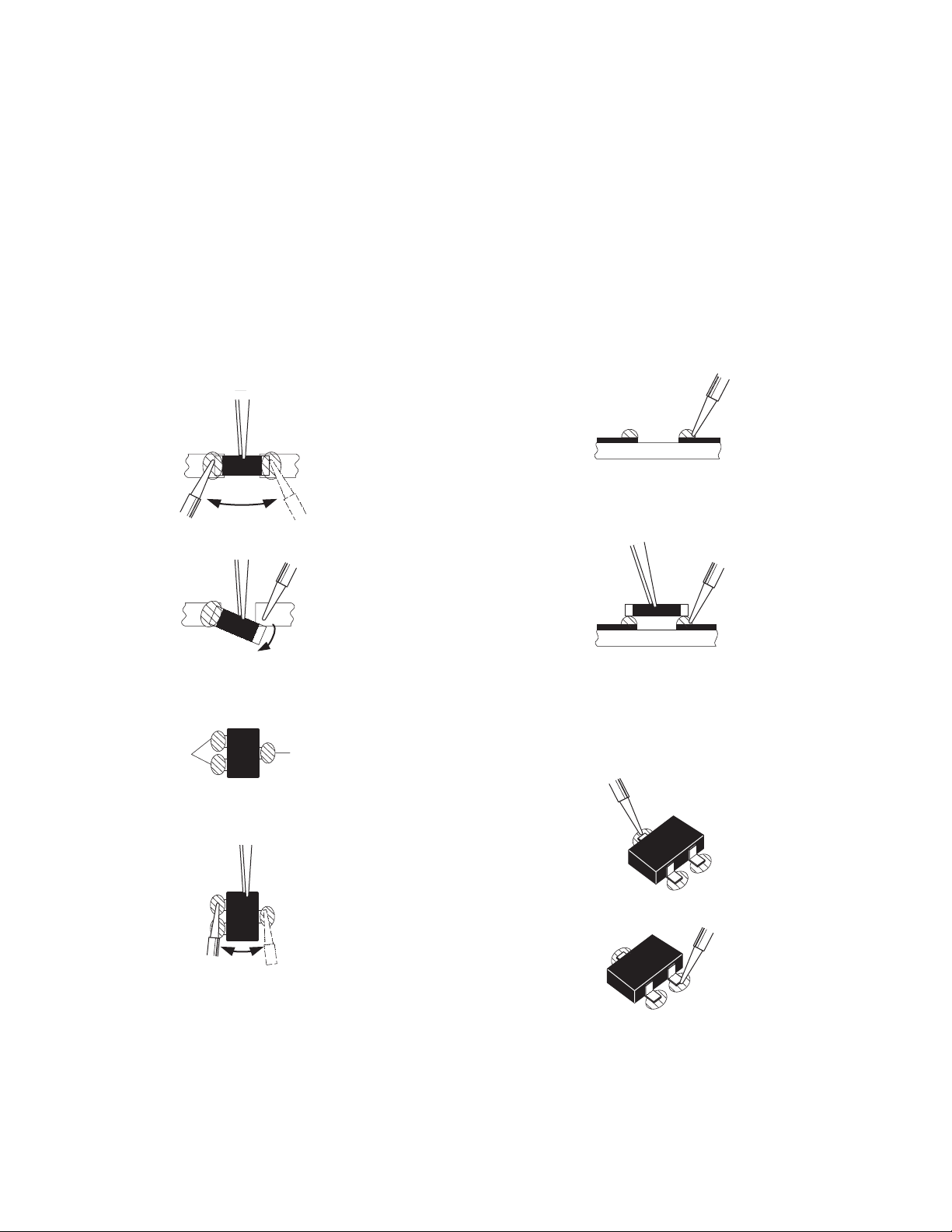
3.3 REPLACEMENT OF CHIP COMPONENT
3.3.1 CAUTIONS
(1) Avoid heating for more than 3 seconds.
(2) Do not rub the electrodes and the resist parts of the pattern.
(3) When removing a chip part, melt the solder adequately.
(4) Do not reuse a chip part after removing it.
3.3.2 SOLDERING IRON
(1) Use a high insulation soldering iron with a thin pointed end of it.
(2) A 30w soldering iron is recommended for easily removing parts.
3.3.3 REPLACEMENT STEPS
1. How to remove Chip parts
2. How to install Chip parts
[Resistors, capacitors, etc.]
(1) As shown in the figure, push the part with tweezers and
alternately melt the solder at each end.
(2) Shift with the tweezers and remove the chip part.
[Transistors, diodes, variable resistors, etc.]
(1) Apply extra solder to each lead.
SOLDER
SOLDER
[Resistors, capacitors, etc.]
(1) Apply solder to the pattern as indicated in the figure.
(2) Grasp the chip part with tweezers and place it on the
solder. Then heat and melt the solder at both ends of the
chip part.
[Transistors, diodes, variable resistors, etc.]
(1) Apply solder to the pattern as indicated in the figure.
(2) Grasp the chip part with tweezers and place it on the
solder.
(3) First solder lead A as indicated in the figure.
(2) As shown in the figure, push the part with tweezers and
alternately melt the solder at each lead. Shift and remove
the chip part.
NOTE :
After removing the part, remove remaining solder from the
pattern.
1-10 (No.YA415)
A
B
C
(4) Then solder leads B and C.
A
B
C
Page 10

SECTION 4
ADJUSTMENT
4.1 ADJUSTMENT PREPARATION
(1) There are 2 ways of adjusting this TV : One is with the
REMOTE CONTROL UNIT and the other is the
conventional method using adjustment parts and
components.
(2) The adjustment using the REMOTE CONTROL UNIT is
made on the basis of the initial setting values. The
setting values which adjust the screen to the optimum
condition can be different from the initial setting
values.
(3) Make sure that connection is correctly made AC to AC
power source.
(4) Turn on the power of the TV and measuring instruments for
warming up for at least 30 minutes before starting
adjustments.
(5) If the receive or input signal is not specified, use the most
appropriate signal for adjustment.
(6) Never touch the parts (such as variable resistors,
transformers and condensers) not shown in the adjustment
items of this service adjustment.
4.2 PRESET SETTING BEFORE ADJUSTMENT
Unless otherwise specified in the adjustment items, preset the
following functions with the REMOTE CONTROL UNIT.
Item Preset value
PICTURE MODE BRIGHT
TINT / COLOUR / BRIGHT / CONT. / SHARP Centre
VNR OFF
BLUE BACK OFF
OFF TIMER OFF
AUTO SHUT OFF OFF
4.3 MEASURING INSTRUMENT AND FIXTURES
(1) DC voltmeter (or digital voltmeter)
(2) Oscilloscope
(3) Signal generator
(Pattern generator : PAL / SECAM / NTSC)
(4) Remote control unit
4.4 ADJUSTMENT ITEMS
CHECK ITEM
• B1 VOLTAGE check
TUNER / IF CIRCUIT
• IF VCO adjustment
• DELAY POINT adjustment
FOCUS
• FOCUS adjustment
DEFLECTION CIRCUIT
• V.HEIGHT / V.POSITION adjustment
• H. POSITION adjustment
• V.LINEARITY / V.S-CURVE adjustment
VIDEO CIRCUIT
• WHITE BALANCE adjustment
• SUB BRIGHT adjustment
• SUB CONTRAST adjustment
• SUB COLOUR adjustment
• SUB TINT adjustment
• SECAM BALACK OFFSET adjustment
VSM PRESET SETTING
• VSM PRESET setting
(No.YA415)1-11
Page 11

4.5 ADJUSTMENT LOCATIONS
F901
TOP
CRT SOCKET PWB
TP-47G/R
T
IC701
(SOLDER SIDE)
U
TP-47B
TP-E
E1
CRT EARTH WIRE
(BRAIDED ASS'Y)
FRONT
IC702
MEMORY IC
PW
DEG
MAIN PWB
TU001
IC301
T
1Pin TP-91(B1)
2Pin NC
3Pin X-ray1
4Pin X-ray2
5Pin TP-E( )
S1
51
U
HV
HVT
UPPER:FOCUS
LOWER:SCREEN
1-12 (No.YA415)
Page 12

4.6 BASIC OPERATION OF SERVICE MENU
4.6.1 TOOL OF SERVICE MENU OPERATION
Operate the SERVICE MENU with the REMOTE CONTROL UNIT.
4.6.2 SERVICE MENU ITEMS
With the SERVICE MENU, various adjustments can be made, and they are broadly classified in the following items of settings.
1.IF Adjustment of the IF circuits.
2.V/C Adjustment of the VIDEO circuit.
3.DEF Adjustment of the DEFLECTION circuit.
4.VSM PRESET Adjustment of the initial setting values of VSM condition as STANDARD, SOFT and BRIGHT.
5.PRESET Adjustment of the RF circuit [Do not adjust].
6.SETUP TOUR It should be able to select mode (LANGUAGE and AUTO CH PRESET) [Should be OFF].
4.6.3 HOW TO ENTER THE SERVICE MENU
Press the [DISPLAY] key and the [PICTURE MODE] key of
the REMOTE CONTROL UNIT simultaneously. Then enter the
SERVICE MODE SELECT KEY
SERVICE MENU mode as shown in Fig.1.
POWER
SERVICE MENU
1.IF 2.V/C
3.DEF 4.VSM PRESET
5.PRESET
6.SETUP TOUR OFF
1-6 : SELECT DISP : EXIT
************ **.***
*** ** **** ***
Fig.1
4.6.4 HOW TO STORE OF SETTING VALUE
The setting value will be stored automatically when release the
REMOTE CONTROL UNIT keys
DISPLAY key
MENU
- / + key
SYSTEM
COLOUR
TV/VIDEO
OFF
TIMER
CHANNEL
SCAN
DISPLAY
CHANNEL
SOUND
RETURN+
MENU
MENU
PICTURE
123
456
789
0-/
MUTING
VOLUME
MODE
PICTURE
MODE key
NUMBERS
key
--
MENU
/ key
4.6.5 HOW TO EXIT THE SERVICE MENU
When complete the adjustment work, press the [DISPLAY]
key to return to the SERVICE MENU. And then press the
[DISPLAY] key again, return to the normal screen.
4.6.6 SELECTION OF SUB MENU SCREEN
Press one of [1] to [5] keys of the REMOTE CONTROL UNIT
and select the SUB MENU SCREEN form the SERVICE
MENU.
(No.YA415)1-13
Page 13

4.6.7 METHOD OF SETTING
1. IF
[1. VCO]
(1) [1] key Select 1. IF.
(2) [1] key Select 1. VCO.
(3) [MENU /] keys Select setting items.
(4) [MENU - / +] keys Adjust the values of the items.
(5) [DISPLAY] key As you press this key twice, you will return to the SERVICE MENU.
[2. DELAY POINT]
(1) [1] key Select 1. IF.
(2) [2] key Select 2. DELAY POINT.
(3) [MENU - / +] keys Set (adjust) the setting values of the setting items.
(4) [DISPLAY] key When this is pressed twice, you will return to the SERVICE MENU.
NOTE:
When the setting value has been changed, the new value will be stored in memory immediately.
2. V/C, 3. DEF and 4. VSM PRESET
(1) [2] to [4] keys Select one from 2. V/C, 3. DEF and 4. VSM PRESET.
(2) [MENU /] keys Select setting items.
(3) [MENU - / +] keys Adjust the values of the items.
(4) [DISPLAY] key When this is pressed, return to the SERVICE MENU.
NOTE:
When the setting value has been changed, the new value will be stored in memory immediately.
5. PRESET (Do not adjust)
6. SETUP TOUR
(1) By pressing the [6] key, you can change the ON or OFF [should be OFF].
Should be OFF:
If it is ON, when you turn off the power and turn on a power again, the JVC’s logo will be shown
about 15 seconds automatically, and the SETUP TOUR starts.
(2) [MENU - / +] keys Select Language.
(3) [MENU ] key Auto Search.
1-14 (No.YA415)
Page 14

4.6.8 SERVICE MENU FLOW CHART
************ **.***
SERVICE MENU
1. IF
SERVICE MENU
1.IF 2.V/C
3.DEF 4.VSM PRESET
5.PRESET
6.SETUP TOUR OFF
1-6 : SELECT DISP : EXIT
************ **.***
6. SETUP TOUR OFF
*** ** **** ***
ON / OFF
(By pressing [6] key)
IF
1. VCO
2. DELAY POINT
1-2 : SELECT DISP : EXIT
2. V/C
V/C PAL
1. CUTOFF
(G)
(B)
50Hz
/ : SELECT
- / + : OPERATE DISP : EXIT
(R)
* **
* **
* **
3. DEF
VCO (CW)
TOO HIGH
ABOVE REFERENCE
JUST REFERENCE
BELOW REFERENCE
TOO LOW
AFT ADJUST
VCO ADJUST
FINE
DISP : EXIT
DELAY POINT UHF
AGC TAKE-OVER
- / + : OPERATE DISP : EXIT
***.**
MHz
*** (**
*** (**
**
)
)
DEF PAL
1. VER. POSITION
50Hz
/ : SELECT
- / + : OPERATE DISP : EXIT
**
4. VSM PRESET
BRIGHT
TINT
COLOUR
BRIGHT
CONT.
SHARP
/ : SELECT
- / + : OPERATE DISP : EXIT
**
**
**
**
**
5. PRESET
PRESET PAL
1. C-TRAP FIX
*
50Hz B/G
/ : SELECT
- / + : OPERATE DISP : EXIT
(No.YA415)1-15
Page 15

4.7 INITIAL SETTING VALUE OF SERVICE MENU
• Adjustment of the SERVICE MENU is made on the basis of the initial setting values ; however, the new setting values which
set the screen in its optimum condition may differ from the initial setting.
• Do not change the initial Setting Values of the Setting (Adjustment) items not listed in "ADJUSTMENT PROCEDURE".
[2. V/C]
Setting item Variable range
1.CUT OFF RED -128 - +127 -50 -50 -50 -50
GREEN -128 - +127 -50 -50 -50 -50
BLUE -128 - +127 -50 -50 -50 -50
2.DRIVE RED -128 - +127 +0 +0 +0 +0
BLUE -128 - +127 +0 +0 +0 +0
3.BRIGHT -128 - +127 +0 +0 +0 +0
4.CONT. -63 - +63+0+0+0+0
5.COLOUR -63 - +63 +0 +0 +0 -5
6.TINT TV -63 - +63 --- --- --- ---
VIDEO -63 - +63 --- --- +0 -2
7.SECAM BL ADJUST -31 - +31 +0 +0 +0 +0
8.SHARP
(Do not adjust)
[3. DEFLECTION]
1. VER. POSITION -4 - +3 -1 -3
2. HOR. POSITION -16 - +15 +3 +3
3. VER. HEIGHT -64 - +63 -35 +1
4. VER. LINEARITY -32 - +31 +15 -1
5. VER. SCURVE -32 - +31 -32 +0
6. HOR. VCO ADJUST
TV -31 - +31 +2 (Fixed) +2 (Fixed) +2 (Fixed) +2 (Fixed)
VIDEO -31 - +31 +15 (Fixed) +15 (Fixed) +15 (Fixed) +15 (Fixed)
Setting item Variable range
[Do not adjust]
-63 - +63 +0 +0
PAL SECAM NTSC 3.58 NTSC 4.43
Initial setting value
fv : 50Hz fv : 60Hz
Initial setting value
[4.VSM PRESET]
Setting item Variable range
TINT 0 - 30 15 15 15
COLOUR 0 - 30 15 15 15
BRIGHT 0 - 30 15 15 15
CONT. 0 - 30 30 15 11
SHARP 0 - 30 15 15 12
1-16 (No.YA415)
BRIGHT STANDARD SOFT
Initial setting value
Page 16

[5. PRESET]
The items in the following table, it is no requirement for adjustment.If values had changed by the miss operation, set the
initial setting values in the following table.
z COLOUR SYSTEM (Do not adjust)
Setting item Variable range
1. C TRAP FIX 0 - 1 1 1 1 1
2. SHARP PEAK 0 - 1 0 0 0 0
3. ABL 0 - 11111
4. GAMMA 0 - 1 0 0 0 0
5. Y. DELAY TIME TV 0 - 3 0 2 2 3
VIDEO 0 - 30202
6. BLACK EXP START 0 - 3 3 3 3 3
7. C-BPFTV 0 - 11100
VIDEO 0 - 11111
8. CW / SCP 0 - 1 0 0 0 0
9. VIF DET LEVEL -63 - +63 +0 +0 +0 +0
11. IF AGC MIN 0 - 1 0 0 0 0
12. VIF AGC 0 - 1 0 0 0 0
13. VIF PMOD 0 - 1 0 0 0 0
19. VNR 0 - 63 15 15 15 15
20. RGB LIM 0 - 1 1 1 1 1
21. RGB LIMIT LEVEL 0 - 7 2 2 2 2
23. TEXT H. POSITION -16 - +15 -3 -3 -3 -3
24. READ DATA --- --- --- --- ---
PAL SECAM NTSC 3.58 NTSC 4.43
Initial setting value (Fixed value)
z SOUND SYSTEM (Do not adjust)
Setting item Variable range
10. SIF DET LEVEL -7 - +7 +0 +0 +0 +0
14. SIF BPF BW ADJUST -7 - +7 +0 +0 +0 +0
15. SIF TRAP FO ADJUST -7 - +7 +0 +0 +0 +0
16. SIF TRAP FO ADJUST 2 -7 - +7 +0 +0 +0 +0
17. SIF -TRAP 0 - 10000
18. SIF -BPF 0 - 10001
22. SIF SW 0 - 11110
B/G I D/K M
Initial setting value (Fixed value)
(No.YA415)1-17
Page 17

4.8 ADJUSTMENT PROCEDURE
4.8.1 CHECK ITEM
Item
B1 VOLTAGE Signal
Measuring
instrument
generator
DC voltmeter
TP-B1 : 1-pin
TP-E : 5-pin
(S1 connector)
[MAIN PWB]
4.8.2 TUNER / IF CIRCUIT
Test point Adjustment part Description
(1) Receive a whole black signal.
(2) Connect a DC voltmeter to 1-pin and 5-pin of S1
connector.
(3) Make sure that the voltage is DC116.2V±2.0V.
Item
Measuring
instrument
IF VCO Signal
generator
Remote
control unit
VCO (CW)
TOO HIGH
ABOVE REFERENCE
JUST REFERENCE
BELOW REFERENCE
TOO LOW
AFT ADJUST
VCO ADJUST
FINE
DISP : EXIT
ADJUSTMENT AT THIS POINT
IS USELESS
***.**
Test point Adjustment part Description
[1. IF]
1. VCO
• Please use a signal generator which frequency output is
correctly calibrated.
(1) Receive any broadcast.
(2) Select 1.IF from the SERVICE MENU.
(3) Select < 1.VCO >.
(4) Select VCO ADJUST with [MENU /] key.
MHz
(5) Press [MENU - / +] keys until the colour of the
characters TOO HIGH changes blue to yellow. Then
gradually press the [MENU - / +] keys until the TOO
YELLOW
LOW changes yellow. At this time, confirm that the
value of VCO ADJUST is near +00.
***(**
***(**
)
)
(6) Select AFT ADJUST with [MENU /] key.
(7) Press [MENU - / +] keys until the characters JUST
REFERENCE changes blue to yellow.
(8) Press the [DISPLAY] key three times to return to
normal screen.
TOO HIGH
ABOVE REFERENCE
JUST REFERENCE
BELOW REFERENCE
TOO LOW
ADJUSTMENT POINT
1-18 (No.YA415)
Page 18

Item
DELAY POINT
(AGC)
Measuring
instrument
Test point Adjustment part Description
Signal
generator
Remote
control unit
DELAY POINT UHF
AGC TAKE-OVER **
- / + : OPERATE DISP : EXIT
[1. IF]
2. DELAY POINT
(AGC TAKE-OVER)
(1) Receive a black and white signal (colour off).
(2) Select 1. IF.
(3) Select < 2. DELAY POINT >.
(4) Set the setting values of the setting items as shown
bellow table.
(5) Then adjust the [MENU - / +] keys until video noise
disappears.
(6) Turn to other channels and make sure that there are
no irregularities.
Setting Item
DELAY POINT
(AGC TAKE-OVER)
NTSC3.58
OTHER
4.8.3 FOCUS
Item
Measuring
instrument
FOCUS Signal
generator
Variable range
0 - 127
Initial setting value
45
35
Test point Adjustment part Description
FOCUS VR
[In HVT]
(1) Receive a crosshatch signal.
(2) While watching the screen, adjust the FOCUS VR to
make the vertical and horizontal lines as fine and
sharp as possible.
(3) Make sure that when the screen is darkened, the
lines remain in good focus.
(No.YA415)1-19
Page 19

4.8.4 DEFLECTION CIRCUIT
• There are 2 modes of adjustment (setting value) 50Hz mode and 60Hz mode, depending upon the kind of signals (vertical frequency
50Hz / 60Hz).
• When adjusted in 50Hz mode and 60Hz mode will be automatically set.
The setting (adjustment) using the REMOTE CONTROL UNIT is made on the basis of the initial setting values.The setting
values which adjust the screen to the optimum condition can be different from the initial setting values.
• Make sure that the adjustment is properly done on the screen of 60Hz mode.
NOTE:
• Adjust to make both 50Hz & 60Hz are the same v. size and fine straight line.
• When adjust again, adjust 50Hz mode first.
• When adjust in 60Hz mode, only 60Hz mode is adjust.
Item
V. HEIGHT /
V. POSITION
Measuring
instrument
Signal
generator
Remote
control unit
Test point Adjustment part Description
[3. DEF]
1. VER. POSITION
3. VER. HEIGHT
(1) Receive a crosshatch signal.
(2) Select 3. DEF from the SERVICE MENU.
(3) Select < 1. VER. POSITION >.
(4) Set the initial setting value of < 1. VER. POSITION >.
(5) Adjust < 1. VER. POSITION > to make the vertical
centre fall on the display centre.
(6) Select <3. VER. HEIGHT >.
(7) Set the initial setting value of <3. VER. HEIGHT >.
Screen
size
Picture
size
100%
(8) Adjust <3. VER. HEIGHT > to make the vertical
screen size be 92% of the picture size.
H. POSITION Signal
generator
Remote
control unit
V.LINEARITY /
V.S-CURVE
Signal
generator
Remote
control unit
(A)
Fig.1
Fig.2
[3. DEF]
2. HOR. POSITION
(B)
[3. DEF]
4. VER. LIN.
5. VER. SCURVE
Top
Centre
(1) Receive a circle pattern signal.
(2) Select 3. DEF from the SERVICE MENU.
(3) Select < 2. HOR. POSITION >.
(4) Set the initial setting value of < 2. HOR. POSITION >.
(5) Adjust <2.HOR. POSITION> to be equal the width of
(A) and (B) as shown in Fig.2.
• If the vertical linearity is noticeably deteriorated, perform
the following steps.
(1) Receive a crosshatch signal.
(2) Select 3. DEF from the SERVICE MENU.
(3) Select < 4. VER. LIN. >.
(4) Set the initial setting value of < 4. VER. LIN. >.
(5) Select < 5. VER. SCURVE >.
(6) Set the initial setting value of < 5. VER. SCURVE >.
(7) Adjust < 4. VER. LIN. > and < 5. VER. SCURVE >
so that the space of upper and lower lines as shown
in Fig.3 on TOP, CENTRE and BOTTOM become
uniform.
1-20 (No.YA415)
Bottom
Fig.3
Page 20

4.8.5 VIDEO CIRCUIT
The setting (adjustment) using the REMOTE CONTROL UNIT is made on the basis of the initial setting values. The setting
values which adjust the screen to the optimum condition can be different from the initial setting values. Do not change the
initial setting values of the setting items not listed in "ADJUSTMENT PROCEDURE".
Item
WHITE
BALANCE
(LOW LIGHT)
Measuring
instrument
Signal
generator
Remote
control unit
Test point Adjustment part Description
[2.V/C]
1. CUT OFF (R)
1. CUT OFF (G)
1. CUT OFF (B)
SCREEN VR
[IN HVT]
(1) Receive a black and white signal (colour off).
(2) Select 2. V/C from the SERVICE MENU.
(3) Select < 1. CUT OFF >.
(4) Set the initial setting value of < 1. CUT OFF >.
(5) Press the [1] key to show the single horizontal line
on screen.
(6) Turn the SCREEN VR fully counter-clockwise, then
slowly turn it clockwise to where one of a red, blue or
KEY ASSIGNMENT OF REMOTE CONTROL UNIT
green colour is faintly visible.
(7) Adjust the two colors which did not appear until the
CUTOFF OFF
(H.LINE OFF)
CUTOFF ON
(H.LINE ON)
R. CUTOFF( )
R. CUTOFF( )
123
456
789
G.CUTOFF( )
B. CUTOFF( )
B. CUTOFF( )
G.CUTOFF( )
single horizontal line that is displayed becomes
white using the [4] to [9] keys.
(8) Turn the SCREEN VR to where the single horizontal
line glows faintly.
(9) Press the [2] key to turn off the single horizontal line.
(10) Press the [DISPLAY] key twice to return to the nor-
mal screen.
R G B
WHITE
BALANCE
(HIGH LIGHT)
Signal
generator
Remote
control unit
KEY ASSIGNMENT OF REMOTE CONTROL UNIT
R. DRIVE( )
SUB BRIGHT Remote
control unit
SUB
CONTRAST
Remote
control unit
123
456
789
R B
[2.V/C]
2. DRIVE (R)
2. DRIVE (B)
B. DRIVE( )
B. DRIVE( )R. DRIVE( )
[2. V/C]
3. BRIGHT
[2. V/C]
4. CONT.
(1) Receive a black and white signal (colour off).
(2) Select 2. V/C from the SERVICE MENU.
(3) Select < 2. DRIVE >.
(4) Set the initial setting value of < 2. DRIVE >.
(5) Adjust the screen until it becomes white using the
[4], [6], [7] and [9] keys.
(6) Press the [DISPLAY] key twice to return to the nom-
al screen.
(1) Receive any broadcast.
(2) Select 2. V/C from the SERVICE MENU.
(3) Select < 3. BRIGHT >.
(4) Set the initial setting value of < 3. BRIGHT >.
(5) If the brightness is not the best with the initial setting
value, make fine adjustment until you get the best
brightness.
(1) Receive any broadcast.
(2) Select 2. V/C from the SERVICE MENU.
(3) Select < 4. CONT >.
(4) Set the initial setting value of < 4. CONT >.
(5) If the contrast is not the best with the initial setting
value, make fine adjustment until you get the best
contrast.
(No.YA415)1-21
Page 21

Item
Measuring
instrument
SUB COLOUR Remote
control unit
Signal
generator
Oscilloscope
Remote
control unit
W
Y
MODEL
AV-21B16
Test point Adjustment part Description
[2. V/C]
5. COLOUR
(PAL / SECAM / NTSC)
TP-47G/R
TP-E
[CRT SOCKET
[2. V/C]
5. COLOUR
(PAL / SECAM / NTSC)
PWB]
B
R
M
0V
(A)
C
G
PAL SECAM NTSC3.58 NTSC4.43
+12V +6V +8V (VDO) ---
(+)
Voltage setting (A)
[Method of adjustment without measuring instrument]
PAL COLOUR
(1) Receive a PAL broadcast.
(2) Select 2. V/C from the SERVICE MENU.
(3) Select < 5. COLOUR >.
(4) Set the initial setting value of < 5. COLOUR >.
(5) If the colour is not the best with the initial setting
value, make fine adjustment until you get the best
colour.
SECAM COLOUR
(1) Receive a SECAM broadcast.
(2) Make fine adjustment of SECAM COLOUR as
previously.
NTSC 3.58 COLOUR
(1) Receive a NTSC 3.58MHz broadcast.
(2) Make similar fine adjustment of NTSC 3.58
COLOUR as previously.
NTSC 4.43 COLOUR
(1) When NTSC 3.58 adjustment completed, NTSC
4.43 will be automatically set at the respective
values.
[Method of adjustment using measuring instrument]
PAL COLOUR
(1) Receive a PAL full field colour bar signal (75%
white).
(2) Select 2. V/C from the SERVICE MENU.
(3) Select < 5. COLOUR >.
(4) Set the initial setting value of < 5. COLOUR >.
(5) Connect the oscilloscope between TP-47G/R and
TP-E.
(6) Adjust PAL COLOUR to bring the value of (A) in
the voltage table.
SECAM COLOUR
(1) Receive a SECAM full field colour bar signal (75%
white).
(2) Set the initial setting value of SECAM COLOUR .
(3) Adjust SECAM COLOUR to bring the value of (A)
in the voltage table.
NTSC 3.58 COLOUR
(1) Receive a NTSC 3.58 full field colour bar signal
(75% white).
(2) Set the initial setting value of NTSC 3.58
COLOUR.
(3) Adjust NTSC 3.58 COLOUR to bring the value of
(A) in the voltage table.
NTSC 4.43 COLOUR
(1) When NTSC 3.58 is set, NTSC 4.43 will be
automatically set at the respective values.
1-22 (No.YA415)
Page 22

Item
Measuring
instrument
SUB TINT Signal
generator
Remote
control unit
Signal
generator
Oscilloscope
Remote
control unit
Test point Adjustment part Description
[2. V/C]
6. TINT
[Method of adjustment without measuring instrument]
NTSC 3.58 TINT
(1) Receive a NTSC 3.58 full field colour bar signal
(75% white).
(2) Select 2. V/C from the SERVICE MENU.
(3) Select < 6. TINT >.
(4) Set the initial setting value of < 6. TINT >.
(5) If you cannot get the best tint with the initial setting
value, make fine adjustment until you get the best
tint.
NTSC 4.43 TINT
(1) When NTSC 3.58 is set, NTSC 4.43 will be
automatically set at the respective values.
TP-47G/R
TP-E
[CRT SOCKET
PWB]
[2. V/C]
6. TINT
[Method of adjustment using measuring instrument]
NTSC 3.58 TINT
(1) Receive a NTSC 3.58 full field colour bar signal
(75% white).
(2) Select 2. V/C from the SERVICE MENU.
(3) Select < 6. TINT >.
(4) Set the initial setting value of < 6. TINT >.
(5) Connect the oscilloscope between TP-47G/R and
TP-E.
B
R
M
(6) Adjust NTSC 3.58 TINT to bring the value of (B)
in the voltage table in the left.
NTSC 4.43 TINT
(1) When NTSC 3.58 is set, NTSC 4.43 will be
(-)
automatically set at the respective values.
AV-21B16
SECAM BLACK
OFFSET
W
MODEL
Signal
generator
Remote
control unit
Y
C
G
Voltage setting (B)
NTSC3.58 NTSC4.43
+6V (VDO) ---
0V
(B)
(+)
[2. V/C]
7. SECAM BL ADJUST
(1) Input a SECAM full field colour bar signal.
(2) Select 2. V/C from the SERVICE MENU.
(3) Select < 7. SECAM BL ADJUST >.
(4) Set the initial setting value of < 7. SECAM BL
ADJUST >.
(5) Switch the [1] key (colour OFF) and [2] key (colour
ON) and make sure that there is no colour on the
black and white screen.
(6) If the black and white screen is not best with the
initial setting value, make fine adjustment until you
get the best black and white screen.
(7) While watching the screen, adjust the value to be the
same colour between ON & OFF by [1] or [2] key.
(8) Press the [DISPLAY] key twice to return to the
normal screen.
(No.YA415)1-23
Page 23

4.8.6 VSM PRESET SETTING
Item
Measuring
instrument
VSM PRESET Remote
control unit
TINT **
COLOUR **
BRIGHT **
CONT.
SHARP **
/ : SELECT
- / + : OPREATE DISP : EXIT
[4.VSM PRESET]
Test point Adjustment part Description
[4. VSM PRESET]
TINT
COLOUR
BRIGHT
CONT.
SHARP
(1) Select 4. VSM PRESET from the SERVICE MENU.
(2) Set the PICTURE MODE to BRIGHT.
(3) Select < TINT >.
(4) Set the initial setting value of < TINT > as shown in
the below table.
(5) Select < COLOUR > to < SHARP > in turn, and set
the values.
(6) Respectively select the "SOFT" and "STANDARD".
BRIGHT
**
Make similar adjustment as same step as above.
Setting
item
Variable
range
Initial setting value
BRIGHT
STANDARD
SOFT
TINT 0 - 30 15 15 15
COLOUR 0 - 30 15 15 15
BRIGHT 0 - 30 15 15 15
CONT. 0 - 30 30 15 11
SHARP 0 - 30 15 15 12
1-24 (No.YA415)
Page 24

4.8.7 PURITY AND CONVERGENCE
PURITY ADJUSTMENT
Note:
The final adjustment of CONVERGENCE must be done after
the FOCUS adjustment. (CONVERGENCE is changed by
FOCUS adjustment.)
When makes difference by FOCUS adjustment, should be
reconfirming PURITY adjustment.
(1) Demagnetize CRT with the demagnetizer.
(2) Loosen the retainer screw of the deflection yoke.
CRT
WEDGE
DEFLECTION
YOKE
P
4 6
P / C
MAGNETS
(3) Remove the wedges.
(4) Input a green raster signal from the signal generator, and
turn the screen to green raster.
(5) Move the deflection yoke backward.
(6) Bring the long lug of the purity magnets on the short lug and
position them horizontally. (Fig.2)
(7) Adjust the gap between two lugs so that the GREEN
RASTER will come into the centre of the screen. (Fig.3)
(8) Move the deflection yoke forward, and fix the position of the
deflection yoke so that the whole screen will become green.
(9) Insert the wedge to the top side of the deflection yoke so that
it will not move.
(10) Input a crosshatch signal.
• P/C MAGNETS
P : PURITY MAGNET
4 : 4 POLES (convergence magnets)
6 : 6 POLES (convergence magnets)
Fig.1
PURITY MAGNETS
Long lug
Short lug
Bring the long lug over the short lug
and position them horizontally.
Fig.2
(FRONT VIEW)
GREEN RASTER
(11) Verify that the screen is horizontal.
(12) Input red and blue raster signals, and make sure that purity
is properly adjusted.
CENTRE
Fig.3
(No.YA415)1-25
Page 25

STATIC CONVERGENCE ADJUSTMENT
(1) Input a crosshatch signal.
(2) Using 4-pole convergence magnets, overlap the red and
blue lines in the centre of the screen (Fig.1) and turn them
to magenta (red/blue).
(3) Using 6-pole convergence magnets, overlap the magenta
(red/blue) and green lines in the centre of the screen and
turn them to white.
(4) Repeat 2 and 3 above, and make best convergence.
DYNAMIC CONVERGENCE ADJUSTMENT
(1) Move the deflection yoke up and down and overlap the lines
in the periphery. (Fig. 2)
(2) Move the deflection yoke left to right and overlap the lines in
the periphery. (Fig. 3)
(3) Repeat 1 and 2 above, and make best convergence.
(4) Adjust XV by XV coil. (Fig.4)
(FRONT VIEW)
Fig.1
(FRONT VIEW)
GREEN
RED
RED
BLUE
BLUE
GREEN
Fig.2
(FRONT VIEW)
GREEN GREEN
RED
BLUE
BLUE
BLUE
RED
GREENGREEN
BLUE
RED
RED
RED
GREEN
BLUE
• After adjustment, fix the wedge at the original position. Fasten
the retainer screw of the deflection yoke. Fix the P/C magnets
with glue.
SECTION 5
TROUBLESHOOTING
This service manual does not describe TROUBLESHOOTING.
(FRONT VIEW)
Xv
BLUE
GREEN
RED
Fig.3
GREEN
Fig.4
1-26 (No.YA415)
Page 26

BLOCK DIAGRAM
MAIN PWB(1/3, 2/3)
STB_PW
IC703
5V REG.& RESET
POWER LED
FRONT IN
REAR IN
VIDEO
AUDIO
VIDEO
AUDIO
TU001
TUNER
SCL/SDA
IF
IC702
MEMORY
Q102
IF AMP
MICRO COMPUTER
SCL/SDA
IC701
SF102
SAW FILTER
SAW
SCL/SDA
EXT
RGB/YS
IC301
1CHIP DECODER
VIDEO IN
AUDIO IN
LED(TIM)
REMOCON
AUDIO OUT
R OUT
G OUT
B OUT
IC651
AUDIO AMP
TIMER LED
REMOCON
RECEIVER
HEADPHONE
SPEAKER L
SPEAKER R
MAIN PWB(3/3)
Q351
R OUT
Q352
G OUT
Q353
B OUT
CRT
REAR OUT
VIDEO
AUDIO
AC IN
POWER SW
LF901
D901
IC921
POWER
REG.
T921
SW
TRANSF.
IC971
9V REG.
IC972
5V REG.
VIDEO OUT
AUDIO OUT
9V OUT
5V OUT
V OUT
H OUT
IC421
V OUT
Q521
H DRIVE
Q522
H OUT
DEF YOKE
(V)
(H)
T522
FBT
B1
EHV
SCREEN
FOCUS
2-4(No.YA415)(No.YA415)2-3
Page 27

CIRCUIT DIAGRAMS
MAIN PWB CIRCUIT DIAGRAM (1/3) SHEET1
POWER LED(GREEN)
ON TIMER LED(RED)
R749
4.7k
R796
X
10k
R750
X
C732
C712
.01
R746
10k
*4
D707
A.PROT
IC704
C727
R771
.1/16
0
1/50
3.9k
R741
560
C744
.01
IC701
*
X
X
X
C733
C735
C734
1k
R708
R709
R710
4.7k
X
R734
R706
560
4.7k
X
OSD_YS
OSD_G
OSD_B
A_MUTE
X
C726
VOL
X
D706
R748
1k
R719
C725
X
P_ON/OFF
C719
C738
X
100
R740
X
C731
.01
C718
C720
.01
C723
3.58/OTH
MAIN PWB ASS'Y(1/3)
SCG-1546A-H2
R711
R773
4.7k
OSD_R
560
CN10A
CN00A
C736
R718
D704
R772
390
Q708
Q710
*3
1k
R725
X
560
R707
560
*3
C730
.01
1k
R729
C717
.01
C713
180p
C716
180p
Y705
K701
R715
R716
680
680
SCL1
SDA1
S702
S701
R726
4.7k
10k
R721
C728
180p
C729
180p
5.6
L701
X701
C711
C710
100/16
.01
S704
S703
R727
15k 4.7k
C721
.033
R737
R728
100k
1k
K703
K704
C709
.01
R738
10k
C722
100p
Q702
*1
R714
4.7k
R720
4.7k
R713
4.7k
R712
4.7k
PIC_MUTE
R730
R731
10K
R736
82k
IC702
R739
10k
Q703
*1
R742
56k
C724
R797
15k
150p
SDA1
AFT
V_SYNC
R723
STB_PW
CP701
S705
J005
IC703
R662 R661
270 270
PIC_MUTE
D731
*4
FBP
100/16
R306
C708
1000/10
C707
.01
LB
R655
47k
Y976
D305
D501
C504
*6
X
V_OUT
C309
C308
R401
.01
0
C402
10K
X
C437
C401
.47
.1
C706
.01
C705
470/16
27
R307
1.2k
R308
1.8k
X
R667
100
Q653
*2
D657
*4
C503 C502
10/50 .01
C316
10/50
SPEAKER
CN0S5
Y658
R327
4.7M
R666
100
D653
R654
22k
Q652
R323
10k
C313
3.3/50
*4
Y656
4.7/50
*1
C659
.027/25
Y657
Q651
R321
1.5k
Q301
*2
C322
R322
2.7k
X
R660 C654
15k 470/16
R653
330
C653
10/50
R651
4.7k
C651
*1
C314
.01
Y301
x
Y302
0
C317
.047/25
220/25
R659
4.7
C658
100/16
C162
1500p
R668
5.6
D652 D651
*7 *4
R664
6.8k
R652
1k
C652
.047
A_MUTE
AUDIO
LINE_A
C315
R324
1k
C324
33/50
D301
*5
C323
0.47/50
A.PROT
A_GND
A_VCC
VIDEO
R163
C164
*
R325
C161
X
*
R161
*
CF161
*
Y160
X
Q161
R165
**
R162 R164
R166
*
CF162
*
*
*
*
C166
*
*
C165
IC701
CF161
CF162
Q161
R161
R162
R163
R164
R165
R166
C114
C161
C164
C165
C166
TU001
*
X
X
X
X
X
X
X
X
X
.01
X
X
X
X
X
X
X
X
X
X
1K
X
1.2K
X
2.2K
X
X
220
22
X
X
820
0.1
X
X
.01
X
.01
.01
X
.1
X
X
X
X
X
X
X
X
X
X
X
X
X
X
X
X
0.1
0.1
X
X
X
X
X
X
X
X
Y655
X
Y654
X
Y653
X
IC651
D655
*4
C664
100/16
D654
*7
D656
*4
C657
100/25
C321
R503
6.8k
D303
R658
2.2k
12p
X302
D306
H_OUT
C663
.001
C655
10/50
C656
1/50
R665
10k
R656
8.2k
C665
.01
R657
2.2k
VOL
LINE_V
Q302
*1
1k
R314
.47/50
1k
H_VCC
BW
0
R501
R502
IC301
C312
R313
0
C501
47/25
.01
C310
220p
R312
C311
FRONT
REAR
REAR
OUT
AFT
C119
J006
X
IN
IN
J004
J003
R802
75
470/16
C841
1500p
C842
X
C805
220/16
C806
R807
68
R815
180
Q804
*1
VIDEO
1
AUDIO
R810
56
Q803
R811
220
LINE_V
R806
270
C811
1
10/50
R816
R817
LINE_A
680
4.7k
A_MUTE
C812
X
J002
NOTE) 1.Refer to the parts list for the part number of IC702.
OSD_YS
Y161
Y975
Y001
Y002
R374
6.8K
STB_PW
STB_PW
A_GND
A_GND
A_VCC
X_RAY5VA_VCC
X_RAY
P_ON/OFF
A.PROT
P_ON/OFF
A.PROT
FBP
FBP
H_VCC
H_VCC
H_OUT
H_OUT
V_OUT
V_OUT
2
2
V_SYNC
SCL1
V_SYNC
R301
0
C301
C341
680P
10/50
D341
C302
*4
4.7/50
R302
4.7k
SCL1
SDA1
9V
OSD_R
C365
1/50
R341
3.3K
C306
.01
ABL
OSD_G
OSD_B
C366
C367
1/50
1/50
C307
470/16
CN00T
MAIN PWB ASS'Y(3/3)
(CRT SOCKET)
R303
100
100
R304
CN10T
C303
C304
10p
100
R305
8.2
L103
47/25
SF102
C109
C305
.47/50
.47/50
X301
C113
.0047
C112
C114
*
C111
X
R118
R116
X
X
Q103
X
X
.01
C326
C115
220p
L104
X
C110
0
.01
220
C116
C122
.01
R121
SF101
X
C121
.01
R114 R109
X 6 .8k
D102
R117
X
C108
X
32V
.47/50
C120
120p
C117
R120
390
.22
C325
R326D302
100*5
10/50
SF122
L101
C106
C107
.0047
.0047
Q102
*10
R115
X
C105
.0047
R159
180k
R160
X
R158
X
R111
180
R112
10
R110
2.7k
R113
100
C104
.0047
CF103
C103
47/25
R103
10
X
3.58/OTH
CF102
L001
8.2
C003
x
C004
470/16
IC001
L002
X
C005
.1
X
R001
X
C009
X
X
R102
K001
10/50
D001
C002
.01
C006
X
R002
220
R003
220
C007
R004
X
56k
c21251001a.001_1/2
TU001
*
75
C001
C008
4.7/50
MAIN PWB(2/3) SHEET2
(No.YA415)2-5 2-6(No.YA415)
Page 28

MAIN PWB CIRCUIT DIAGRAM (2/3)(3/3) SHEET 2
AC110V-AC240V
50Hz/60Hz
!
CN0PW
!
VA901
!
S901
!
220
D931
F901
T3.15AL
RY971
X
!
C991
!
C992
.001
R901
!
C904
.001
D901
C929
!
C905
.001
C909
*
R903
R934
68k
*4
D921
R935
.01
R928
68k
C930
X
K901
*8
D933
*5
D925
D930
K902
*8
R933
4.7
*5
!
C993
!
R991
8.2M
DEG COIL
!
CNDEG
R904
IC921
Y904
Y905
!
C901
!
LF901
!
TH901
*
D928
Y903
!
C910
!
C907
.001
R923
R921
1.8
100k
R922
1M
R925
D927
R924
150K
*7
C925
33/50
3.9k
C926
3300p
*
Y902
R906
100k
C931
C927
C924
.1/50
4.7/50
X
R929
D929
C922
X
.1
C932
220p
D920
Q973
MAIN PWB(1/3) SHEET 1
STB_PW
A_GND
LB
A_VCC
Y973
0
Y961
R985
X
D973
X
R986
C972
X
K941
T921
X
R987
D974 R988
X
XX
560p
D942
D941
C941
D943
C944
C947
CP981
L943
4.7
!
*5
CP982
C945
1000/25
C948
1000/25
C949
470p
L942
C942
100/160
1000/25
L941
4.7
C946
82
CN0S2
!
!
K943
*8
K942
*8
*8
X
Q961
X
R961
R962
X
X
IC971
IC972
Q974
H004
R963
X
R964
X
C977
220/16
C979
X
220/10
R974
2.2k
C971
X
D986
X
Q982
Q962
X
R976
12
C976
220/25
R979
47
C978
220/25
R978
47k
R977
1.2k
Q975
*3
X
5V
H_VCC
Y972
X
R965
X
C961
X
D982
*4
D983
*4
R984
X
R983
Q981
X
R982
X
X
R981
X
32V
X_RAY
A.PROT
9V
P_ON/OFF
X
D985
X
C981
X
H_OUT
R980
15K
Q572
*1
ABL
V_OUT
V_SYNC
FBP
R422
R421
4.7k
X
R423
0
D424
X
R424
0
R425
C422
3.3k
X
V_OUT
Q402
R436
82k
*1
D427
Q401
R524
X
R525
C523
33
47/25
Q521
R531
R532
330
100/160
D571
C572
R578
10k
47/25
D562
XX
C561
R565
X
IC421
C427
100/35
C423
18p
R426
0
C424
R443
1
C436
.33
D425
*4
C429
10/50
.0033
1k
C531
R566
X
XX
C529
R573
C426
.001
R441
.01
R453
3.3K
R576
R577
8.2k
R432
3.9
T501
R526
270
R530
X
C526
.0082
R529
C530
R528
R574
R575
X
22k
Q571
D561
C562
K421
!
470
D421
*8
R521
Q522
56
C421
R431
10k
Y502
R571
2.2K
C571
100/10
R433
!
D584
R582
TP-47G/R
TP-47R/G
R349
4.7K
R369
X
X
R583
39k
R552
TP-47B
R581
1.8k
4.7/250
C554
D581
SK351
!
SK351
K351
Y303
Y304
!
X
C909
FOCUS
SCREEN
C351
.001
*
C352
TP-E
X
R365
12k
R368
R364
R367
1.8k
1.8k
R363
R366
T522
L353
R362
C356
390p
R359
R356
470
330
R348
X
12k
L352
R361
C355
270p
R358
R355
330
470
12k
L351
R360
R347
3.9K
C354
330p
R357
R354
1.8k
470
330
L354
CN10U
CN00U
!
R584
C581
.1
R585
D582
X
*5
C553
X
D552
*5
Q353
R353
150
Q352
R352
150
R345
X
CN10T
C357
470/10
X
R346
R351
150
D352
D353
Q351
MAIN PWB ASS'Y(3/3)
(CRT SOCKET)
X
R442
C433
4.7/50
C435
2200/25
10k
.0047
100/35
D423
C430
C428
*6
R430
82k
10k
R429
C425
X
CN00T
XXX
MAIN PWB ASS'Y(1/3)
R444
X
D351
SCG-1546A-H2
R440
*
C525
C528
X
C582
X
D555
X
X
Y501
C527
X
L522
26V
!
D554
*4
R554
680
R551
C552
1000/35
D553
C555
.1/100
C551
D551
L551
FR556
X
*5
X
MAIN PWB ASS'Y(2/3)
Y503
X
CN0S1
CN0HV
SCG-1546A-H2
c21251001a.001_2/2
ADJUSTMENT
CONNECTOR
2-8(No.YA415)(No.YA415)2-7
!
DEF YOKE
Page 29

PATTERN DIAGRAMS
MAIN PWB PATTERN
()
C927
W229
R906
W028
IC921
D927
D929
CNDEG
R904
C925
R921
R903
S901
C931
H003
R923
C554
CN00U
W548
C552
C421
C423
R4 30
D423
R429
D553
W106
W175
W634
CN0S5
R661
R573
R574
R571
C553
R552
D552
R585
W657
W016
D582
W017
FRONT
R582
IC421
D427
R551
R431
R441
W337
R347
R367
D581
W129
R424
C422
W105
D352
D421
H001
R425
D425
D354
K351
CN00T
D355
R583
W071
T522
C551
B1
D551
R433
R432
R444
D356
R358
Y304
C424
R453
C429
W576
C433
D353
R3
55
C355
K421
W495
R352
Y303
C357
R345
C430
C435
Y503
Q352
R529
R361
R440
L522
W476
C582
TP-E
CN0HV
H002
Y502
Y501
R528
C525
Q522
C530
R442
C527
D555
R530
R524
R532
W596
W032
C528
R521
T501
C529
C526
C523
R526
Q521
R525
()
R363
R354
R364
TP-47G/R
R357
C354
W611
R346
R351
L351
R360
52
L3
SCREEN
W336
C351
R366
Q351
TP-47R/G
R368
R356
R3
SK351
C352
R362
R359
C356
Q353
53
L353
R365
()
TOP
L354
CN00U
TP-47B
R369
C581
W605
R581
FR556
C562
D561
C555
C436
R443
W003
W087
W080
C427
90
W5
W635
C42
C426
5
R4
23
D424
Q402
W169
W176
R426
R422
R421
W011
R531
R436
Q401
R349
R348
W338
D351
Y001
R002
W041
R003
W012
C001
C659
C653
W422
W631
D707
W097
W654
W136
TU001
Y002
C007
W099
C003
C664
C663
C658
R652
R659
Y655
Y654
W632
W510
C008
W641
R004
C010
C011
R102
C002
W110
W030
R303
W214
R302
W069
C341
W159
W555
W655
W505
R741
R301
W150
W072
C365
W054
W066
W620
W623
W481
W217
C654
C366
W114
W113
W112
W101
R719
W473
W459
W517
91
R746
R726
C726
12C7
W646
W4
45
W5
R796
R748
C732
R750
C731
S702 S703 S704
R308
W656
W005
W618
C725
D706
CF102
W544
C304
01
20
C744
R802
CN00T
C3
C302
R708
C7
R707
J002
C842
R806
C806
CF103
R103
C109
Q103
C307
R304
R306
W090
Y976
C309
R401
C308
W479
R711
R710
R7
18
R7
09
R734
C7
33
C7
18
R749
R740
R807
R810
C103
C106
R110
C104
R109
Q102
C303
R503
W628
C721
R728
R721
R730
X301
Q703
C111
X302
C501
C723
R114
W117
D731
C722
R111
D306
D303
16
K701
C717
C112
IC301
C504
R738
R739
W120
C730
R729
C114
C312
C311
C716
C113
C321
R715R7
Y705
C713
W523
W602
X7 01
28
C107
C326
R3
22
C402
R714
R720
R725
C7
R731
L1 01
R118
C108
R116
L103
C305
W092
R305
C306
C437
C316
C5
02
C503
C401
R501
D501
R797
W155
Q702
R7 06
C7 36
C734
R737
C7
35
W423
W524
R727
SF101
Q803
C105
R112
D102
K704
R117
L104
C314
R327
R312
C313
R742
C729
Q302
R113
W432
C805
Q804
R817
R816
R815
R811
C811
R115
Y161
C121
C110
SF122
C122
SF102
C117
R121
C115
C116
R160
64
C162
R313
R314
W626
R321
Y972
Y975
C315
C310
R307
C166
C164
Y301
W617
R1
W168
W231
Q301
W604
W174
Y973
W616
C317
D305
C322
C724
W436
C812
W580
W424
R158
C119
C120
R120
R159
R3
D302
C165
R163
R1
65
R166
Q161
C161
R1
61
CF161
D301
W130
C323
R323
W502
W220
Y3
02
W206
D584
D341
W615
R341
W579
26
W095
W124
C325
Y160
R162
CF162
C324
R325
W494
W588
W482
W472
W451
R324
W504
R736
W247
W645
R584
W137
W613
W612
C708
L701
W431
C711
C710
W474
K703
IC701
S705
W496
C709
C705
IC703
C706
C707
IC702
R712
R713
J006
W429
CP701
J004
W413
B
C841
C991
L941
C993
W543
C942
K941
C949
D942
K942
CL003
C944
R978
Q974
R976
R977
W652
R986
D974
R988
Q973
C976 R502
A
R987
73
D9
RY971
K943
C941
C945
W563
IC971
CP982
W103
H004
R984
R983
R981
Q982
D986
C981
D985
D941
C948
CP981
C947
D943
W164
L943
R974
C971
W466
L942
W648
Y961
R9
C946
61
R962
Q975
R963
C961
R965
W014
C972
C977
W188
R979
IC972
C979
R985
D982
W148
W566
R964
D657
Q981
R982
CN0S2
W578
D983
Q961
R668
Q962
W187
W519
R657
W190
R374
W111
W053
R980
C005
C006
C004
D001
L002
L001
W098
K001
C009
IC001
R001
H006
R658
C656
R667
D654
R666
R660
W649
C978
W184
C657
C367
D656
B
IC651
Q653
W204
CN0S3
R655
Y653
R653
C652
D655
C655
W647
W173
CN00A
Q708
R771
CL005
C719
C727
R723
CN00A
R654
W653
C738
R656
C665
C651
Q652
R665
D653
Q651
D652
R664
R651
D651
S701
Q710
D921
D925
35
R9
R925
C926
R929
W023
D931
C922
W329
C924
R924
C932
R934
W049
D933
R933
T921
D928
D920
W227
W228
K901
K902
R922
C905
C909
TH901
Y905
Y904
LF901
C930
D930
W062
C929
C904
D901
C907
W603
R991
Y902
R901
C910
C992
Y903
R928
W061
CN0PW
VA
901
C901
F901
FC902
D704
R772
R773
FC901
IC704
R578
Q572
W009
W162
W195
W196
W198
W199
J003
W077
W094
W412
W201
CN0S1
R565
W411
CN0S4
W154
C531
Y656
C572
D571
J005
W004
R566
L551
D554
W638
W643
W644
C561
Y658
R575
C571
Q571
R577
R576
W073
W640
C428
D562
R554
W636
Y657
R662
(No.YA415)2-9 2-10(No.YA415)
Page 30

VOLTAGE CHARTS
<MAIN PWB>
MODE
PIN NO.
IC301
1 0
2 4.4
3 6.3
4 3.4
5 0
6 5.0
7 5.0
8 5.5
9 9.0
10 3.0
11 3.0
12 3.0
13 0
14 2.8
15 4.2
16 9.0
17 3.8
18 2.8
19 2.8
20 0
21 0
22 0
23 4.4
24 3.2
25 3.0
26 3.5
27 4.2
28 3.7
29 4.1
30 3.9
31 4.2
32 4.2
33 9.0
34 4.0
35 4.7
36 4.0
37 6.1
38 4.2
39 4.3
40 2.7
41 6.2
42 1.0
43 3.7
44 3.9
45 1.2
46 3.1
47 5.4
48 5.0
49 0.7
50 0
51 4.4
52 0.7
IC421
1 3.7
2 26.0
3 2.0
4 0
5 13.8
6 26.3
7 3.7
IC651
1 12.5
2 5.6
3 0
4 2.4
5 9.4
6 9.6
7 0
8 9.7
9 19.9
IC701
1 4.5
2 4.9
3 0
4 0
5 0
6 4.9
7 4.9
8 2.3
9 3.0
10 4.9
11 0
12 0
13 2.4
14 0.1
15 1.8
16 1.8
17 0
18 0.8
19 0
20 4.9
21 4.9
22 4.9
23 4.9
24 2.3
25 4.9
DC (V
MODE
)
PIN NO.
26 0
27 4.1
28 4.9
29 0
30 0
31 0
32 0
33 0
34 4.9
35 4.7
36 4.9
37 4.4
38 4.4
39 4.9
40 0
41 2.1
42 0
IC702
1 0
2 0
3 0
4 0
5 4.9
6 4.9
7 0
8 4.9
IC703
1 14.4
2 5.8
3 0
4 4.9
5 4.9
IC704
1 4.5
2 4.9
3 0
IC921
1 314.0
2 NC
3 0
4 0
5 31.8
6 0
7 0.7
IC971
1 12.8
2 9.0
3 0
IC972
1 9.2
2 4.9
3 0
Q102
E 0
C 9.0
B 2.3
Q103
E 0
C 0
B 4.0
Q161
E 2.5
C 8.3
B 3.2
Q301
E 4.6
C 0
B 4.0
Q302
E 4.0
C 9.0
B 4.6
Q401
E 0
C 0
B 5.4
Q402
E 0
C 4.9
B 0
Q521
E 0
C 9.7
B 0.3
Q522
E 0
C 115.3
B 0
Q571
E 115.5
C 0
B 115.1
Q572
E 0
C 4.9
B 0
DC (V
MODE
)
PIN NO.
Q651
E 0
C 0.3
B 0
Q652
E 0
C 1.0
B 0.6
Q653
E 15.1
C 0
B 15.2
Q702
E 0
C 4.2
B 0
Q703
E 0
C 4.8
B 0.1
Q708
E 0
C 2.0
B 0
Q710
E 0
C 0.1
B 0
Q803
E 0
C 8.1
B 4.7
Q804
E 0
C 0
B 0.1
Q974
E 15.3
C 15.1
B 0
Q975
E 0
C 0.1
B 4.3
TU001
1 4.6
2 NC
3 0
4 4.4
5 0
6 4.5
7 4.9
8 0
9 31.3
10 NC
11 0
DC (V
<CRT SOCKET PWB>
MODE
)
PIN NO.
Q351
E 2.5
C 125.8
B 3.2
Q352
E 2.6
C 123.3
B 3.3
Q353
E 2.5
C 128.5
B 3.2
DC (V
)
(No.YA415)2-11
Page 31

WAVEFORMS
-MAIN PWB-
(SHEET1)
IC301-10
IC301-11
(H)
(H)
IC301-12
(H)
IC301-14
(1µs)
IC301-36
(H)
IC301-40
(1µs)
IC301-42
(H)
3.5 Vp-p
IC301-46
2.5 Vp-p
(SHEET2)
IC421-1
0.6 Vp-p
Q522-B
2.0 Vp-p
(V)
(V)
(H)
IC701-27
5.0 Vp-p
IC421-3
T522-1
1000 Vp-p
3.5 Vp-p
30 Vp-p
(H)
(V)
(H)
IC701-35
5.0 Vp-p
IC421-5
60 Vp-p
T522-3
4.0 Vp-p
55Vp-p
(V)
(V)
(H)
IC421-6
T522-5
0.35 Vp-p
30 Vp-p
220 Vp-p
(V)
(H)
Q521-C
T522-7
3.0 Vp-p
38 Vp-p
25 Vp-p
(H)
(H)
Q521-B
T522-9
0.5 Vp-p
1.5 Vp-p
220Vp-p
(H)
(H)
Q522-C
2.5 Vp-p
(H)
1000Vp-p
-CRT SOCKET PWB-
(SHEET2)
Q351-C Q352-C Q353-C
110 Vp-p
(H)
120 Vp-p
2-12(No.YA415)
(H) (H)
120 Vp-p
Page 32

CONTENTS
USING P.W. BOARD & REMOTE CONTROL UNIT ................................................................................................... 3-3
EXPLODED VIEW PARTS LIST -1 ............................................................................................................................. 3-3
EXPLODED VIEW -1 ................................................................................................................................................... 3-4
PRINTED WIRING BOARD PARTS LIST ................................................................................................................... 3-5
MAIN P.W. BOARD ASS'Y (SCG-1546A-H2) .................................................................................................... 3-5
REMOTE CONTROL UNIT PARTS LIST (RM-C360GY-1H) ..................................................................................... 3-8
PACKING ..................................................................................................................................................................... 3-8
PACKING PARTS LIST ............................................................................................................................................... 3-8
3-2(No.YA415)
Page 33

USING P.W. BOARD & REMOTE CONTROL UNIT
P.W.B ASS'Y AV-21B16
MAIN P.W.B SCG-1546A-H2
REMOTE CONTROL UNIT RM-C360GY-1H
EXPLODED VIEW PARTS LIST -1
Ref.No. Part No. Part Name Description Local
V01 A51MBA11X05AN05 PICTURE TUBE(ITC) Inc.DEF YOKE, PC MAGNET
L01 QQW0125-001 DEG COIL
T522 QQH0170-001 FB TRANSF
1 GG30152-001A-H JVC MARK
2 GG30150-002A-H OPERATION SHEET
3 GG30149-001A-H LED LENS
11 QYSBSFG4016ZA TAP SCREW M4 x 16mm(x6)
12 QYSBSF3010ZA TAP SCREW M3 x 10mm
13 QYSBSFG4016ZA TAP SCREW M4 x 16mm
14 GG10421-002B-H REAR COVER
15 CM47005-A01-H POWER CORD CLAMP
16 QMPR340-165-K2 POWER CORD 1.65m BLACK
17 GG30119-001B-H SUB PCB HOLDER
18 A48457-3-H SPRING
19 WJY0008-006A-E BRAIDED ASS'Y
20 GG30151-001A-H CHASSIS RAIL (x2)
21 QYSBSF4012ZA TAP SCREW M4 x 12mm(x4)
22 QAS0347-001 SPEAKER (x2) SP01,SP02
30 SCG-1546A-H2 MAIN PWB
100 GG10419-002B-H FRONT CABINET ASS'Y Inc.101,102,103
101 GG20131-001B-H DOOR
102 GG30148-001B-H POWER KNOB
103 CM35235-003-H SPRING
(No.YA415)3-3
Page 34

EXPLODED VIEW -1
3
101
18
L01
22
21
V01
15
19
17
16
20
22
CRT SOCKET PWB
30
(Within MAIN PWB)
FRONT LED PWB
30
(Within MAIN PWB)
21
1
2
102
T522
103
30
MAIN PWB
100
3-4(No.YA415)
14
11
RATING LABEL
13
12
Page 35

PRINTED WIRING BOARD PARTS LIST
MAIN P.W. BOARD ASS'Y (SCG-1546A-H2)
Ref No. Part No. Part Name Description Local
IC301 NN5198K IC
IC421 LA78040N IC
IC651 AN5265 IC
IC701 MN1873287JL1 IC
IC702 ATE08-21YMG6 IC (SERVICE)
IC703 L78LR05E-MA IC
IC704 GP1UM281QK IR DETECT UNIT 38kHz
IC921 STR-W5753A/F5 IC
IC971 L7809CP IC
IC972 L7805CP IC
Q102 2SC5397/CD/-T TRANSISTOR
Q301 2SA1530A/QR/-X TRANSISTOR
Q302 2SC3928A/QR/-X TRANSISTOR
Q351 2SC4212/Z1/ TRANSISTOR
Q352 2SC4212/Z1/ TRANSISTOR
Q353 2SC4212/Z1/ TRANSISTOR
Q401 DTC124ESA-T DIGI TRANSISTOR
Q402 2SC3928A/QR/-X TRANSISTOR
Q521 2SC2655/Y/-T TRANSISTOR
Q522 2SD2627-YB11 POW TRANSISTOR
Q571 2SA1208/ST/Z1-T TRANSISTOR
Q572 2SC3928A/QR/-X TRANSISTOR
Q651 2SC3928A/QR/-X TRANSISTOR
Q652 2SC3928A/QR/-X TRANSISTOR
Q653 2SA1530A/QR/-X TRANSISTOR
Q702 2SC3928A/QR/-X TRANSISTOR
Q703 2SC3928A/QR/-X TRANSISTOR
Q708 UN2212-X DIGI TRANSISTOR
Q710 UN2212-X DIGI TRANSISTOR
Q803 KTC3199/YG/-T TRANSISTOR
Q804 2SC3928A/QR/-X TRANSISTOR
Q974 2SA966/OY/-T TRANSISTOR
Q975 UN2212-X DIGI TRANSISTOR
D001 MTZJ33A-T2 Z DIODE
D301 MTZJ9.1B-T2 Z DIODE
D302 MTZJ9.1B-T2 Z DIODE
D303 MA3091/M/-X Z DIODE
D305 1K4-T2 SB DIODE
D306 QRE121J-561Y C RESISTOR 560Ω 1/2W J
D341 MA111-X SI DIODE
D421 MTZJ75-T2 Z DIODE
D423 1SR124-400A-T2 SI DIODE
D425 MA111-X SI DIODE
D427 MTZJ27B-T2 Z DIODE
D501 MTZJ6.8C-T2 Z DIODE
D551 FR105GT-T3 SI DIODE
D552 FR105GT-T3 SI DIODE
D553 MTZJ9.1B-T2 Z DIODE
D554 MA111-X SI DIODE
D571 MTZJ7.5S-T2 Z DIODE
D581 MTZJ20B-T2 Z DIODE
D582 FR105GT-T3 SI DIODE
D651 MA111-X SI DIODE
D652 MTZJ12C-T2 Z DIODE
D653 MA111-X SI DIODE
D654 MTZJ12C-T2 Z DIODE
D655 MA111-X SI DIODE
D656 MA111-X SI DIODE
D657 MA111-X SI DIODE
D704 SPR-39MVWF LED
D707 MA111-X SI DIODE
D731 MA111-X SI DIODE
D901 G2SBA60 BRIDGE DIODE
D920 1SS133-T2 SI DIODE
D921 FR105GT-T3 SI DIODE
D925 FR105GT-T3 SI DIODE
D927 MTZJ36A-T2 Z DIODE
D928 MTZJ3.3A-T2 Z DIODE
D930 FR107GT-T3 SI DIODE
D931 MA111-X SI DIODE
D933 MTZJ16C-T2 Z DIODE
D941 RU3AM-LFC4 SI DIODE
D942 ERC30-02L38E SI DIODE
D943 FR105GT-T3 SI DIODE
D982 MA111-X SI DIODE
D983 MA111-X SI DIODE
C001 QETN1HM-106Z E CAPACITOR 10uF 50V M
C002 NCB31HK-103X C CAPACITOR 0.01uF 50V K
C004 QETN1CM-477Z E CAPACITOR 470uF 16V M
POWER,ON TIMER(RED-GREEN)
Ref No. Part No. Part Name Description Local
C005 QFVF1HJ-104Z MF CAPACITOR 0.1uF 50V J
C008 QETN1HM-475Z E CAPACITOR 4.7uF 50V M
C103 QETN1EM-476Z E CAPACITOR 47uF 25V M
C104 NCB31HK-472X C CAPACITOR 4700pF 50V K
C105 NCB31HK-472X C CAPACITOR 4700pF 50V K
C106 NCB31HK-472X C CAPACITOR 4700pF 50V K
C107 NCB31HK-472X C CAPACITOR 4700pF 50V K
C110 NRSA63J-0R0X MG RESISTOR 0Ω 1/16W J
C112 QETN1EM-476Z E CAPACITOR 47uF 25V M
C113 NCB31HK-472X C CAPACITOR 4700pF 50V K
C114 NCB31HK-103X C CAPACITOR 0.01uF 50V K
C115 NCB31HK-103X C CAPACITOR 0.01uF 50V K
C116 NCB31HK-103X C CAPACITOR 0.01uF 50V K
C117 QFVF1HJ-224Z MF CAPACITOR 0.22uF 50V J
C119 QETN1HM-474Z E CAPACITOR 0.47uF 50V M
C120 NDC31HJ-121X C CAPACITOR 120pF 50V J
C121 NCB31HK-103X C CAPACITOR 0.01uF 50V K
C122 NCB31HK-103X C CAPACITOR 0.01uF 50V K
C162 NCB31HK-152X C CAPACITOR 1500pF 50V K
C301 NCB31HK-123X C CAPACITOR 0.012uF 50V K
C302 QETN1HM-475Z E CAPACITOR 4.7uF 50V M
C303 NDC31HJ-100X C CAPACITOR 10pF 50V J
C304 QFVF1HJ-474Z MF CAPACITOR 0.47uF 50V J
C305 QETN1HM-474Z E CAPACITOR 0.47uF 50V M
C306 NCB31HK-103X C CAPACITOR 0.01uF 50V K
C307 QETN1CM-477Z E CAPACITOR 470uF 16V M
C308 QETN1CM-107Z E CAPACITOR 100uF 16V M
C309 NCB31HK-103X C CAPACITOR 0.01uF 50V K
C310 NDC31HJ-221X C CAPACITOR 220pF 50V J
C311 NCB31HK-103X C CAPACITOR 0.01uF 50V K
C312 QENC1HM-474Z BP E CAPACITOR 0.47uF 50V M
C313 QETN1HM-335Z E CAPACITOR 3.3uF 50V M
C314 NCB31HK-103X C CAPACITOR 0.01uF 50V K
C315 QETN1CM-107Z E CAPACITOR 100uF 16V M
C316 QETN1HM-106Z E CAPACITOR 10uF 50V M
C317 NCB31EK-473X C CAPACITOR 0.047uF 25V K
C321 NDC31HJ-120X C CAPACITOR 12pF 50V J
C322 NCB31EK-273X C CAPACITOR 0.027uF 25V K
C323 QETN1HM-474Z E CAPACITOR 0.47uF 50V M
C324 QETN1HM-336Z E CAPACITOR 33uF 50V M
C325 QENC1HM-106Z BP E CAPACITOR 10uF 50V M
C326 NCS21HJ-221X C CAPACITOR 220pF 50V J
C341 QETN1HM-106Z E CAPACITOR 10uF 50V M
C351 QCZ0340-332 C CAPACITOR 3300pF 2kV K
C354 NDC31HJ-331X C CAPACITOR 330pF 50V J
C355 NDC31HJ-271X C CAPACITOR 270pF 50V J
C356 NDC31HJ-391X C CAPACITOR 390pF 50V J
C357 QETN1AM-477Z E CAPACITOR 470uF 10V M
C365 QENC1HM-105Z BP E CAPACITOR 1uF 50V M
C366 QENC1HM-105Z BP E CAPACITOR 1uF 50V M
C367 QENC1HM-105Z BP E CAPACITOR 1uF 50V M
C401 QFVF1HJ-474Z MF CAPACITOR 0.47uF 50V J
C423 QCS32HJ-180Z C CAPACITOR 18pF 500V J
C424 QFLC2AJ-103Z M CAPACITOR 0.01uF 100V J
C426 QFLC1HJ-102Z M CAPACITOR 1000pF 50V J
C427 QETN1VM-107Z E CAPACITOR 100uF 35V M
C428 QETN1VM-107Z E CAPACITOR 100uF 35V M
C429 QETN1HM-106Z E CAPACITOR 10uF 50V M
C430 QFN32AJ-472Z M CAPACITOR 4700pF 100V J
C433 QEHR1HM-475Z E CAPACITOR 4.7uF 50V M
C435 QETM1EM-228 E CAPACITOR 2200uF 25V M
C436 QFVF1HJ-334Z MF CAPACITOR 0.33uF 50V J
C437 NCB31HK-104X C CAPACITOR 0.1uF 50V K
C501 QETN1EM-476Z E CAPACITOR 47uF 25V M
C502 NCB31HK-103X C CAPACITOR 0.01uF 50V K
C503 QETN1HM-106Z E CAPACITOR 10uF 50V M
C523 QETN1EM-476Z E CAPACITOR 47uF 25V M
C525 QFZ0200-962 MPP CAPACITOR 9600pF 1.5kV H
C526 QFLC1HJ-822Z M CAPACITOR 8200pF 50V J
C527 QFZ0197-274 MPP CAPACITOR 0.27uF 250V J
C529 QFLC1HJ-332Z M CAPACITOR 3300pF 50V J
C530 QCB32HK-561Z C CAPACITOR 560pF 500V K
C531 QEZ0203-107 E CAPACITOR 100uF 160V M
C552 QETM1VM-108 E CAPACITOR 1000uF 35V M
C554 QETN2EM-475Z E CAPACITOR 4.7uF 250V M
C555 QFLC2AJ-104Z M CAPACITOR 0.1uF 100V J
C571 QETN1AM-107Z E CAPACITOR 100uF 10V M
C572 QETN1EM-476Z E CAPACITOR 47uF 25V M
C581 QFVF1HJ-104Z MF CAPACITOR 0.1uF 50V J
C652 NCB31HK-473X C CAPACITOR 0.047uF 50V K
C653 QETN1HM-106Z E CAPACITOR 10uF 50V M
C654 QETN1CM-477Z E CAPACITOR 470uF 16V M
C655 QETN1HM-106Z E CAPACITOR 10uF 50V M
C656 QENC1HM-105Z BP E CAPACITOR 1uF 50V M
(No.YA415)3-5
Page 36

Ref No. Part No. Part Name Description Local
Ref No. Part No. Part Name Description Local
C657 QETN1EM-107Z E CAPACITOR 100uF 25V M
C658 QETN1EM-227Z E CAPACITOR 220uF 25V M
C659 QETN1HM-475Z E CAPACITOR 4.7uF 50V M
C663 NCB31HK-102X C CAPACITOR 1000pF 50V K
C664 QETN1CM-107Z E CAPACITOR 100uF 16V M
C665 NCB31HK-103X C CAPACITOR 0.01uF 50V K
C705 QETN1CM-477Z E CAPACITOR 470uF 16V M
C706 NCB31HK-104X C CAPACITOR 0.1uF 50V K
C707 NCB31HK-103X C CAPACITOR 0.01uF 50V K
C708 QETN1AM-108Z E CAPACITOR 1000uF 10V M
C709 NCB31HK-103X C CAPACITOR 0.01uF 50V K
C710 QETN1CM-107Z E CAPACITOR 100uF 16V M
C711 NCB31HK-103X C CAPACITOR 0.01uF 50V K
C712 NCB31HK-103X C CAPACITOR 0.01uF 50V K
C713 NCB31HK-103X C CAPACITOR 0.01uF 50V K
C716 NDC31HJ-181X C CAPACITOR 180pF 50V J
C717 NDC31HJ-181X C CAPACITOR 180pF 50V J
C718 NCB31HK-103X C CAPACITOR 0.01uF 50V K
C719 QETN1HM-105Z E CAPACITOR 1uF 50V M
C720 NCB31HK-103X C CAPACITOR 0.01uF 50V K
C721 NCB31EK-333X C CAPACITOR 0.033uF 25V K
C722 NDC31HJ-101X C CAPACITOR 100pF 50V J
C724 NDC31HJ-560X C CAPACITOR 56pF 50V J
C727 NCB31CK-104X C CAPACITOR 0.1uF 16V K
C728 NDC31HJ-181X C CAPACITOR 180pF 50V J
C729 NDC31HJ-181X C CAPACITOR 180pF 50V J
C730 NCB31HK-103X C CAPACITOR 0.01uF 50V K
C744 NCB31HK-103X C CAPACITOR 0.01uF 50V K
C805 QETN1CM-227Z E CAPACITOR 220uF 16V M
C806 QETN1CM-477Z E CAPACITOR 470uF 16V M
C811 QETN1HM-106Z E CAPACITOR 10uF 50V M
C841 NCB31HK-152X C CAPACITOR 1500pF 50V K
C901 QFZ9073-224 MM CAPACITOR 0.22uF AC250V M
C904 QCZ9054-102 C CAPACITOR 1000pF AC250V Z
C905 QCZ9054-102 C CAPACITOR 1000pF AC250V Z
C907 QCZ9054-102 C CAPACITOR 1000pF AC250V Z
C909 QEZ0633-127 E CAPACITOR 120uF 450V M
C910 QFZ9072-104 MM CAPACITOR 0.1uF AC250V K
C922 QFLC1HJ-104Z M CAPACITOR 0.1uF 50V J
C924 QETN1HM-475Z E CAPACITOR 4.7uF 50V M
C925 QETN1HM-336Z E CAPACITOR 33uF 50V M
C926 QFLC1HJ-332Z M CAPACITOR 3300pF 50V J
C927 QFLC1HJ-104Z M CAPACITOR 0.1uF 50V J
C929 QFKA2JK-103 MM CAPACITOR 0.01uF 630V K
C931 QCZ0364-681 C CAPACITOR 680pF 2kV K
C932 NDC31HJ-221X C CAPACITOR 220pF 50V J
C941 QCZ0364-561 C CAPACITOR 560pF 2kV K
C942 QEZ0203-107 E CAPACITOR 100uF 160V M
C944 QCB32HK-222Z C CAPACITOR 2200pF 500V K
C945 QEHR1EM-108Z E CAPACITOR 1000uF 25V M
C946 QETN1EM-108Z E CAPACITOR 1000uF 25V M
C947 QCB32HK-222Z C CAPACITOR 2200pF 500V K
C948 QETN1EM-108Z E CAPACITOR 1000uF 25V M
C949 NDC31HJ-471X C CAPACITOR 470pF 50V J
C976 QETN1EM-227Z E CAPACITOR 220uF 25V M
C977 QETN1CM-227Z E CAPACITOR 220uF 16V M
C978 QETN1EM-227Z E CAPACITOR 220uF 25V M
C979 QETN1AM-227Z E CAPACITOR 220uF 10V M
C991 QCZ9071-102 C CAPACITOR 1000pF AC400V M
C992 QCZ9071-102 C CAPACITOR 1000pF AC400V M
C993 QCZ9071-102 C CAPACITOR 1000pF AC400V M
R002 NRSA63J-221X MG RESISTOR 220Ω 1/16W J
R003 NRSA63J-221X MG RESISTOR 220
R004 NRSA63J-563X MG RESISTOR 56k
R102 NRSA63J-750X MG RESISTOR 75
R103 NRSA63J-100X MG RESISTOR 10
R109 NRSA63J-682X MG RESISTOR 6.8k
R110 NRSA63J-272X MG RESISTOR 2.7k
R111 NRSA63J-181X MG RESISTOR 180
R112 NRSA63J-100X MG RESISTOR 10
R113 NRSA63J-101X MG RESISTOR 100Ω 1/16W J
R120 NRSA63J-391X MG RESISTOR 390
R121 NRSA63J-221X MG RESISTOR 220
R159 NRSA63J-184X MG RESISTOR 180kΩ 1/16W J
R301 NRSA63J-0R0X MG RESISTOR 0
R302 NRSA63J-472X MG RESISTOR 4.7kΩ 1/16W J
R303 NRSA63J-101X MG RESISTOR 100
R304 NRSA63J-101X MG RESISTOR 100Ω 1/16W J
R305 NRSA63J-101X MG RESISTOR 100
R306 NRSA63J-0R0X MG RESISTOR 0Ω 1/16W J
R307 NRSA63J-122X MG RESISTOR 1.2k
R308 NRSA63J-182X MG RESISTOR 1.8k
R312 NRSA63J-0R0X MG RESISTOR 0Ω 1/16W J
R313 NRSA63J-102X MG RESISTOR 1kΩ 1/16W J
R314 NRSA63J-102X MG RESISTOR 1k
R321 NRSA63J-152X MG RESISTOR 1.5k
Ω
1/16W J
Ω
1/16W J
Ω
1/16W J
Ω
1/16W J
Ω
1/16W J
Ω
1/16W J
Ω
1/16W J
Ω
1/16W J
Ω
1/16W J
Ω
1/16W J
Ω
1/16W J
Ω
1/16W J
Ω
1/16W J
Ω
1/16W J
Ω
1/16W J
Ω
1/16W J
Ω
1/16W J
R322 NRSA63J-272X MG RESISTOR 2.7kΩ 1/16W J
R323 NRSA63J-103X MG RESISTOR 10kΩ 1/16W J
R324 NRSA63J-102X MG RESISTOR 1kΩ 1/16W J
R326 NRSA63J-101X MG RESISTOR 100Ω 1/16W J
R327 NRSA63J-475X MG RESISTOR 4.7MΩ 1/16W J
R341 NRSA63J-332X MG RESISTOR 3.3kΩ 1/16W J
R347 NRSA63J-392X MG RESISTOR 3.9kΩ 1/16W J
R349 NRSA63J-472X MG RESISTOR 4.7kΩ 1/16W J
R351 NRSA63J-151X MG RESISTOR 150Ω 1/16W J
R352 NRSA63J-151X MG RESISTOR 150Ω 1/16W J
R353 NRSA63J-151X MG RESISTOR 150Ω 1/16W J
R354 NRSA63J-331X MG RESISTOR 330Ω 1/16W J
R355 NRSA63J-331X MG RESISTOR 330Ω 1/16W J
R356 NRSA63J-331X MG RESISTOR 330Ω 1/16W J
R357 NRSA63J-470X MG RESISTOR 47Ω 1/16W J
R358 NRSA63J-470X MG RESISTOR 47Ω 1/16W J
R359 NRSA63J-470X MG RESISTOR 47Ω 1/16W J
R360 QRZ0107-152Z C RESISTOR 1.5kΩ 1/2W K
R361 QRZ0107-152Z C RESISTOR 1.5kΩ 1/2W K
R362 QRZ0107-152Z C RESISTOR 1.5kΩ 1/2W K
R363 QRL029J-123 OMF RESISTOR 12kΩ 2W J
R364 QRL029J-123 OMF RESISTOR 12kΩ 2W J
R365 QRL029J-123 OMF RESISTOR 12kΩ 2W J
R366 NRSA63J-182X MG RESISTOR 1.8kΩ 1/16W J
R367 NRSA63J-182X MG RESISTOR 1.8kΩ 1/16W J
R368 NRSA63J-182X MG RESISTOR 1.8k
R374 NRSA63J-682X MG RESISTOR 6.8k
R401 NRSA02J-103X MG RESISTOR 10kΩ 1/10W J
R421 NRSA63J-472X MG RESISTOR 4.7kΩ 1/16W J
R423 NRSA63J-0R0X MG RESISTOR 0Ω 1/16W J
R424 NRSA63J-0R0X MG RESISTOR 0Ω 1/16W J
R425 NRSA63J-332X MG RESISTOR 3.3kΩ 1/16W J
R426 NRSA63J-0R0X MG RESISTOR 0Ω 1/16W J
R429 NRSA63J-103X MG RESISTOR 10kΩ 1/16W J
R430 NRSA63J-823X MG RESISTOR 82kΩ 1/16W J
R431 NRSA02J-103X MG RESISTOR 10kΩ 1/10W J
R432 QRE121J-3R9Y C RESISTOR 3.9Ω 1/2W J
R433 QRE121J-2R7Y C RESISTOR 2.7Ω 1/2W J
R436 NRSA63J-823X MG RESISTOR 82kΩ 1/16W J
R440 QRE121J-471Y C RESISTOR 470Ω 1/2W J
R441 NRSA63J-822X MG RESISTOR 8.2kΩ 1/16W J
R442 NRSA63J-103X MG RESISTOR 10kΩ 1/16W J
R443 QRE121J-1R0Y C RESISTOR 1Ω 1/2W J
R453 NRSA63J-332X MG RESISTOR 3.3kΩ 1/16W J
R502 NRSA63J-0R0X MG RESISTOR 0Ω 1/16W J
R503 NRSA63J-682X MG RESISTOR 6.8kΩ 1/16W J
R521 QRE121J-560Y C RESISTOR 56Ω 1/2W J
R525 QRL029J-330 OMF RESISTOR 33Ω 2W J
R526 QRE121J-271Y C RESISTOR 270Ω 1/2W J
R528 QRE121J-471Y C RESISTOR 470Ω 1/2W J
R529 QRL039J-681 OMF RESISTOR 680Ω 3W J
R531 NRSA63J-331X MG RESISTOR 330Ω 1/16W J
R532 NRSA63J-102X MG RESISTOR 1kΩ 1/16W J
R551 QRX029J-R47 MF RESISTOR 0.47Ω 2W J
R552 QRJ146J-2R2X UNF C RESISTOR 2.2Ω 1/4W J
R554 QRE121J-681Y C RESISTOR 680
R571 QRE121J-222Y C RESISTOR 2.2kΩ 1/2W J
R573 QRT029J-1R5 MF RESISTOR 1.5
R574 QRT029J-1R5 MF RESISTOR 1.5
R576 QRE121J-223Y C RESISTOR 22kΩ 1/2W J
R577 NRSA63J-392X MG RESISTOR 3.9kΩ 1/16W J
R578 NRSA63J-103X MG RESISTOR 10kΩ 1/16W J
R581 QRE121J-182Y C RESISTOR 1.8kΩ 1/2W J
R582 NRSA63J-273X MG RESISTOR 27k
R583 NRSA63J-393X MG RESISTOR 39k
R651 NRSA63J-472X MG RESISTOR 4.7k
R652 NRSA63J-102X MG RESISTOR 1k
R653 NRSA63J-331X MG RESISTOR 330
R654 NRSA63J-223X MG RESISTOR 22k
R655 NRSA63J-473X MG RESISTOR 47k
R656 NRSA63J-822X MG RESISTOR 8.2k
R657 NRSA63J-222X MG RESISTOR 2.2kΩ 1/16W J
R658 NRSA63J-222X MG RESISTOR 2.2k
R659 QRE121J-4R7Y C RESISTOR 4.7
R660 NRSA63J-153X MG RESISTOR 15kΩ 1/16W J
R661 QRE121J-271Y C RESISTOR 270
R662 QRE121J-271Y C RESISTOR 270Ω 1/2W J
R664 NRSA63J-682X MG RESISTOR 6.8k
R665 NRSA63J-103X MG RESISTOR 10kΩ 1/16W J
R666 NRSA63J-101X MG RESISTOR 100
R667 QRE121J-101Y C RESISTOR 100Ω 1/2W J
R668 QRT029J-5R6 MF RESISTOR 5.6
R706 NRSA63J-561X MG RESISTOR 560
R707 NRSA63J-561X MG RESISTOR 560Ω 1/16W J
R708 NRSA63J-102X MG RESISTOR 1kΩ 1/16W J
R709 NRSA63J-472X MG RESISTOR 4.7k
R710 NRSA63J-472X MG RESISTOR 4.7k
Ω
1/16W J
Ω
1/16W J
Ω
1/2W J
Ω
Ω
Ω
1/16W J
Ω
1/16W J
Ω
1/16W J
Ω
1/16W J
Ω
1/16W J
Ω
1/16W J
Ω
1/16W J
Ω
1/16W J
Ω
1/16W J
Ω
1/2W J
Ω
1/2W J
Ω
1/16W J
Ω
1/16W J
Ω
Ω
1/16W J
Ω
1/16W J
Ω
1/16W J
2W J
2W J
2W J
3-6(No.YA415)
Page 37

Ref No. Part No. Part Name Description Local
Ref No. Part No. Part Name Description Local
R711 NRSA63J-472X MG RESISTOR 4.7kΩ 1/16W J
R712 NRSA63J-472X MG RESISTOR 4.7kΩ 1/16W J
R713 NRSA63J-472X MG RESISTOR 4.7kΩ 1/16W J
R714 NRSA63J-472X MG RESISTOR 4.7kΩ 1/16W J
R715 NRSA63J-681X MG RESISTOR 680Ω 1/16W J
R716 NRSA63J-681X MG RESISTOR 680Ω 1/16W J
R718 NRSA63J-561X MG RESISTOR 560Ω 1/16W J
R719 NRSA63J-102X MG RESISTOR 1kΩ 1/16W J
R720 NRSA63J-472X MG RESISTOR 4.7kΩ 1/16W J
R721 NRSA63J-103X MG RESISTOR 10kΩ 1/16W J
R723 QRL039J-270 OMF RESISTOR 27Ω 3W J
R725 NRSA63J-102X MG RESISTOR 1kΩ 1/16W J
R726 NRSA63J-472X MG RESISTOR 4.7kΩ 1/16W J
R727 NRSA63J-153X MG RESISTOR 15kΩ 1/16W J
R728 NRSA63J-102X MG RESISTOR 1kΩ 1/16W J
R729 NRSA63J-102X MG RESISTOR 1kΩ 1/16W J
R730 NRSA63J-103X MG RESISTOR 10kΩ 1/16W J
R731 NRSA63J-472X MG RESISTOR 4.7kΩ 1/16W J
R736 NRSA63J-823X MG RESISTOR 82kΩ 1/16W J
R737 NRSA63J-104X MG RESISTOR 100kΩ 1/16W J
R738 NRSA63J-103X MG RESISTOR 10kΩ 1/16W J
R739 NRSA63J-103X MG RESISTOR 10kΩ 1/16W J
R740 NRSA63J-392X MG RESISTOR 3.9kΩ 1/16W J
R741 NRSA63J-561X MG RESISTOR 560Ω 1/16W J
R742 NRSA63J-563X MG RESISTOR 56kΩ 1/16W J
R746 NRSA63J-103X MG RESISTOR 10k
R748 NRSA63J-101X MG RESISTOR 100
R749 NRSA63J-472X MG RESISTOR 4.7kΩ 1/16W J
R771 NRSA63J-0R0X MG RESISTOR 0Ω 1/16W J
R772 NRSA63J-391X MG RESISTOR 390Ω 1/16W J
R773 NRSA63J-561X MG RESISTOR 560Ω 1/16W J
R796 NRSA63J-103X MG RESISTOR 10kΩ 1/16W J
R797 NRSA63J-153X MG RESISTOR 15kΩ 1/16W J
R802 NRSA63J-750X MG RESISTOR 75Ω 1/16W J
R806 QRE121J-271Y C RESISTOR 270Ω 1/2W J
R807 NRSA63J-680X MG RESISTOR 68Ω 1/16W J
R810 QRG01GJ-560 OMF RESISTOR 56Ω 1W J
R811 NRSA63J-221X MG RESISTOR 220Ω 1/16W J
R815 QRE121J-181Y C RESISTOR 180Ω 1/2W J
R816 NRSA63J-681X MG RESISTOR 680Ω 1/16W J
R817 NRSA63J-472X MG RESISTOR 4.7kΩ 1/16W J
R901 QRF104K-3R9 UNF WW RESISTOR 3.9Ω 10W K
R903 QRL029J-104 OMF RESISTOR 100kΩ 2W J
R904 QRL039J-151 OMF RESISTOR 150Ω 3W J
R906 QRL029J-104 OMF RESISTOR 100kΩ 2W J
R921 QRE121J-1R8Y C RESISTOR 1.8Ω 1/2W J
R922 QRE121J-221Y C RESISTOR 220Ω 1/2W J
R923 QRZ0237-R18 UNF WW RESISTOR 0.18Ω 3W J
R924 NRSA63J-154X MG RESISTOR 150kΩ 1/16W J
R925 NRSA63J-105X MG RESISTOR 1MΩ 1/16W J
R928 QRL039J-683 OMF RESISTOR 68kΩ 3W J
R933 QRE121J-4R7Y C RESISTOR 4.7Ω 1/2W J
R934 NRSA63J-683X MG RESISTOR 68kΩ 1/16W J
R935 QRE121J-392Y C RESISTOR 3.9kΩ 1/2W J
R974 NRSA63J-222X MG RESISTOR 2.2kΩ 1/16W J
R976 QRL029J-120 OMF RESISTOR 12
R977 QRE121J-122Y C RESISTOR 1.2kΩ 1/2W J
R978 NRSA63J-473X MG RESISTOR 47k
R979 QRL039J-470 OMF RESISTOR 47
R980 QRL029J-153 OMF RESISTOR 15kΩ 2W J
R991 QRZ9046-825Z C RESISTOR 8.2MΩ 1/2W K
L001 QQL244K-8R2Z PEAKING COIL 8.2uH K
L101 QQL244J-2R2Z PEAKING COIL 2.2uH J
L103 QQL244K-8R2Z PEAKING COIL 8.2uH K
L522 QQR1005-002 LINEARITY COIL
L551 QQLZ026-320 COIL 32uH ±7%
L701 QQL244J-5R6Z COIL 5.6uH J
L941 QQL26AK-820Z CHOKE COIL 82uH K
L942 QQL244J-4R7Z PEAKING COIL 4.7uH J
L943 QQL244J-4R7Z PEAKING COIL 4.7uH J
T501 QQR1244-001 DRIVE TRANSF
T921 QQS0213-001 SW TRANSF
CP981 ICP-N50-T IC PROTECTOR 2.0A
CP982 ICP-N75-T IC PROTECTOR 2.7A
F901 QMF51E2-3R15-S FUSE 3.15A AC250V
J002 QNN0384-001 PIN JACK
J003 QNN0281-003 PIN JACK VIDEO IN(FRONT)
J004 QNN0281-002 PIN JACK AUDIO IN(FRONT)
J005 QNS0197-001 3.5 JACK HEADPHONE
K351 QQR0621-002Z FERRITE BEADS
K421 QQR1113-001Z FERRITE BEADS
K901 QQR1113-001Z FERRITE BEADS
K902 QQR1113-001Z FERRITE BEADS
K941 QQR1113-001Z FERRITE BEADS
K942 QQR1113-001Z FERRITE BEADS
Ω
1/16W J
Ω
1/16W J
Ω
2W J
Ω
1/16W J
Ω
3W J
VIDEO,AUDIO IN/OUT(REAR)
K943 QQR1113-001Z FERRITE BEADS
LF901 QQR0527-002 LINE FILTER
S701 QSW0619-003Z PUSH SWITCH CH+
S702 QSW0619-003Z PUSH SWITCH CHS703 QSW0619-003Z PUSH SWITCH VOL+
S704 QSW0619-003Z PUSH SWITCH VOLS705 QSW0619-003Z PUSH SWITCH MENU
S901 QSW0750-001 PUSH SWITCH POWER
SF102 QAX0666-002 SAW FILTER
SF122 QAX0325-001 SAW FILTER
SK351 QNZ0536-002 CRT SOCKET
TH901 QAD0121-9R0 P THERMISTOR 9
TU001 QAU0466-001 TUNER
VA901 QAF0072-621 VARISTOR 620V
X301 QAX0705-001Z CRYSTAL 4.433619MHz
X302 QAX0860-001Z CRYSTAL 3.579545MHz
X701 QAX0884-001 C RESONATOR 12.000MHz
GG30157-001A-H LED HOLDER
Ω
(No.YA415)3-7
Page 38

REMOTE CONTROL UNIT PARTS LIST (RM-C360GY-1H)
Ref No. Part No. Part Name Description Local
R25-8567 BATTERY COVER
PACKING
8
2
4 5 6 7
3
9
2
PACKING PARTS LIST
Ref.No. Part No. Part Name Description Local
1 GG10285-012A-H PACKING CASE
2 GG10422-001A-H CUSHION ASS'Y 5pcs in 1set
3 GG30097-003A-H POLY BAG
4 GG30096-001A-H POLY BAG
5 ------------ BATTERY 1.5V AA/R6 (x2)
6 GGT0106-001B-H INST BOOK
7 GGT0107-001B-H DIGEST MANUAL
8 RM-C360GY-1H REMOCON UNIT
9 GG30147-001B-H CORNER LABEL 2pcs in 1set
9
1
3-8(No.YA415)
 Loading...