

Page 1
SCHEMATIC DIAGRAMS
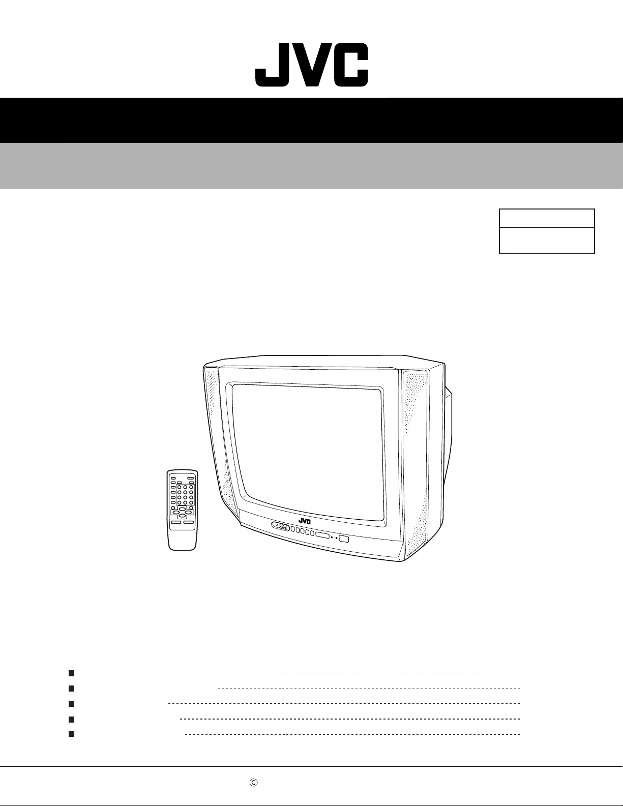
COLOUR TELEVISION
AV-20N41
AV-16N71
AV-20N41/BK
AV-16N71/VT
CD-ROM No.SML200111
BASIC CHASSIS
CG
CONTENTS
NOTE ON USING CIRCUIT DIAGRAMS
SEMICONDUCTOR SHAPES
BLOCK DIAGRAM
CIRCUIT DIAGRAMS
PATTERN DIAGRAMS
COPYRIGHT 2001 VICTOR COMPANY OF JAPAN, LTD.
2-1
2-2
2-3
2-5
2-13
No.51924
Nov. 2001
Page 2
STANDARD CIRCUIT DIAGRAM
NOTE ON USING CIRCUIT DIAGRAMS
1.SAFETY
The components identified by the symbol and shading are
critical for safety. For continued safety replace safety critical
components only with manufactures recommended parts.
2.SPECIFIED VOLTAGE AND WAVEFORM VALUES
The voltage and waveform values have been measured under the
following conditions.
(1)Input signal : Colour bar signal
(2)Setting positions of
each knob/button and
variable resistor
(3)Internal resistance of test er
:DC 20k
/V
(4)Oscilloscope sweeping time
:H
20µS/div
:V
5mS/div
:Others
Sweeping time is
specified
(5)Voltage values
:All DC voltage values
Since the voltage values of signal circuit vary to some extent
according to adjustments, use them as reference values.
3.INDICATION OF PARTS SYMBOL [EXAMPLE]
In the PW board
:R1209
R209
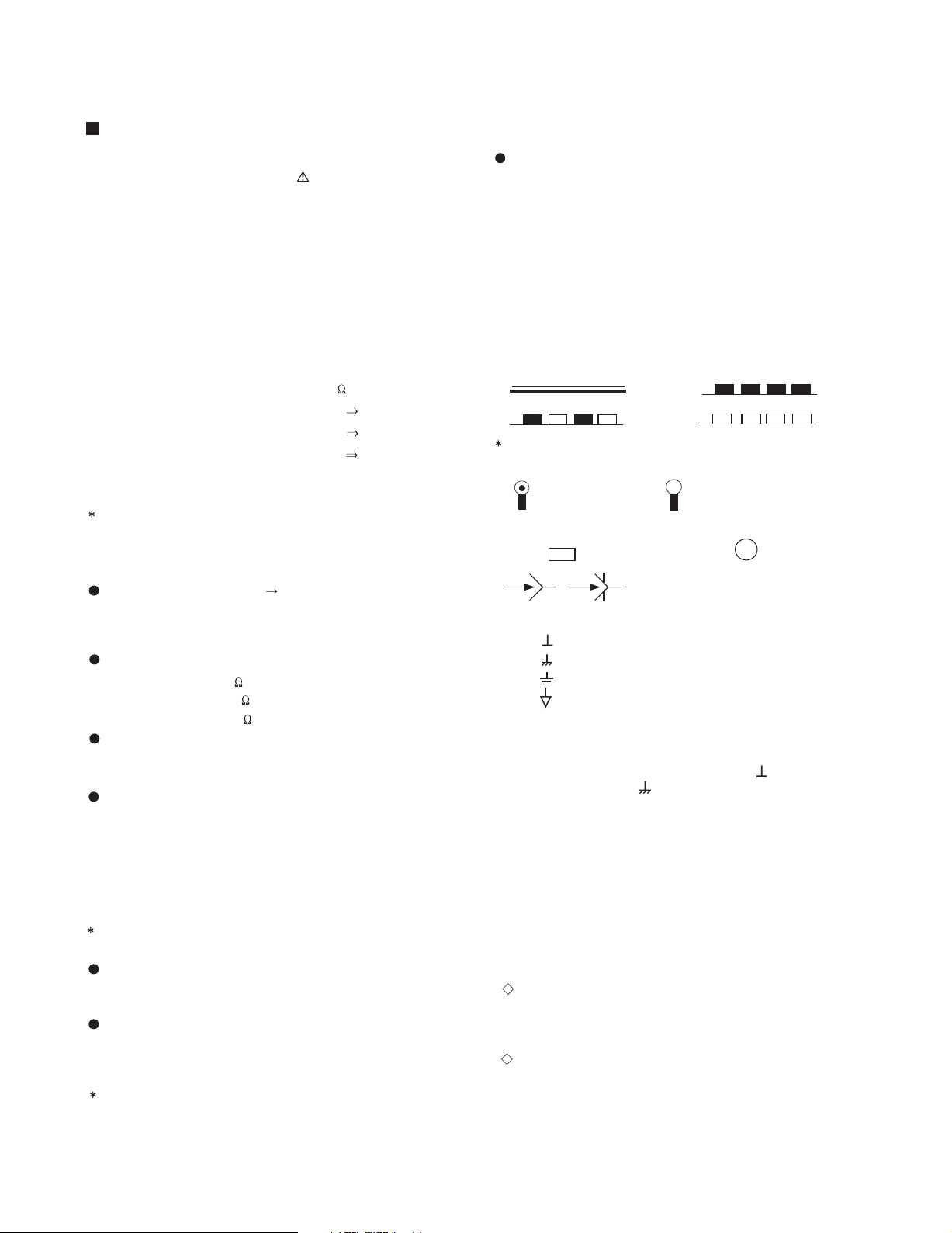
4.INDICATIONS ON THE CIRCUIT DIAGRAM
(1)Resistors
Resistance value
No unit :[
]
K
:[K
]
M
Rated allowable power
No indication :1/ 16 [W]
Others :As specified
Type
No indication
:Carbon resistor
OMR
:Oxide met al fil m resistor
MFR
:Metal film resist or
MPR
:Metal plate resistor
UNFR
:Uninflammable resistor
FR
:Fusible resistor
Composition resistor 1/2 [W] is specified as 1/2S or Comp.
(2)Capacitors
: Original setting position
when shipped
5.NOTE FOR REP AIRING SERVICE
This model's power circuit is par tly different in the GND. The
difference of the GND is shown by the LIVE : ( ) side GND and the
ISOLATED(NEUTRAL) : ( ) side GND.Therefore, care must be
taken for the following points.
(1)Do not touch the LIVE side GND or the LIVE side GND and the
ISOLATED(NEUTRAL) side GND simultaneously. If the above
caution is not respected, an electric shock may be caused.
Therefore, make sure that the power cord is surely removed from
the receptacle when, for example, the chassis is pulled out.
(2)Do not short between the LIVE side GND and ISOLATED(NEUTRAL)
side GND or never measure with a measuring apparatus measure
with a measuring apparatus ( oscilloscope, etc.) the LIVE side GND
and ISOLATED(NEUTRAL) side GND at the same time.
If the above precaution is not respected , a fuse or any parts will be broken.
Since the circuit diagram is a standard one, the circuit and
circuit constants may be subjec t to chang e for improvement
withou t any notice.
NOTE
Due improvement in performance, some part numbers show
in the circuit diagram may not agree with those indicated in
the part list.
When ordering parts, please use the numbers that appear
in the Parts List.
Type
MM
:Metalized mylar capacitor
PP
:Polypropylene ca pacitor
MPP
:Metalized polypropylene capacitor
MF
:Metalized f ilm capacitor
TF
:Thin film capacitor
BP
:Bipolar electrolytic capaci tor
TAN
:Tantalum capacitor
(3)Coils
No unit
:[
µ
H]
Others
:As specified
(4)Power Supply
:B1
:9V
:5V
Respective voltage values are indicated
(5)Test point
:T est po int
:Only test point display
(6)Connec ting method
:Connector
:Wrapping or s oldering
:Receptacle
(7)Ground symbol
:LIVE side ground
:ISOLATED(NEUTRAL) side g round
:EARTH ground
:DIGITAL ground
:[M ]
Capacitance value
1 or higher :[pF]
less than 1
:[µF]
Withstand voltage
No indication :DC 50[V]
Others :DC withstand voltage [V]
AC indicated
:AC withstand voltage [V]
Electrolytic Capacitors
47/50[Example]:Capacitance value [µF]/withstand voltage[V]
No indication :Ceramic capacitor
:B2 (12V)
AV-20N41
AV-16N71
Nov. 2001 No. 51924
Page 3
AV-20N41
STANDARD CIRCUIT DIAGRAM
NOTE ON USING CIRCUIT DIAGRAMS
1.SAFETY
The components identified by the symbol and shading are
critical for safety. For continued safety replace safety critical
components only with manufactures recommended parts.
2.SPECIFIED VOLTAGE AND WAVEFORM VALUES
The voltage and waveform values have been measured under the
following conditions.
(1)Input signal : Colour bar signal
(2)Setting positions of
each knob/button and
variable resistor
(3)Internal resistance of test er
:DC 20k
/V
(4)Oscilloscope sweeping time
:H
20µS/div
:V
5mS/div
:Others
Sweeping time is
specified
(5)Voltage values
:All DC voltage values
Since the voltage values of signal circuit vary to some extent
according to adjustments, use them as reference values.
3.INDICATION OF PARTS SYMBOL [EXAMPLE]
In the PW board
:R1209
R209
4.INDICATIONS ON THE CIRCUIT DIAGRAM
(1)Resistors
Resistance value
No unit :[
]
K
:[K
]
M
Rated allowable power
No indication :1/ 16 [W]
Others :As specified
Type
No indication
:Carbon resistor
OMR
:Oxide met al fil m resistor
MFR
:Metal film resist or
MPR
:Metal plate resistor
UNFR
:Uninflammable resistor
FR
:Fusible resistor
Composition resistor 1/2 [W] is specified as 1/2S or Comp.
(2)Capacitors
: Original setting position
when shipped
5.NOTE FOR REP AIRING SERVICE
This model's power circuit is par tly different in the GND. The
difference of the GND is shown by the LIVE : ( ) side GND and the
ISOLATED(NEUTRAL) : ( ) side GND.Therefore, care must be
taken for the following points.
(1)Do not touch the LIVE side GND or the LIVE side GND and the
ISOLATED(NEUTRAL) side GND simultaneously. If the above
caution is not respected, an electric shock may be caused.
Therefore, make sure that the power cord is surely removed from
the receptacle when, for example, the chassis is pulled out.
(2)Do not short between the LIVE side GND and ISOLATED(NEUTRAL)
side GND or never measure with a measuring apparatus measure
with a measuring apparatus ( oscilloscope, etc.) the LIVE side GND
and ISOLATED(NEUTRAL) side GND at the same time.
If the above precaution is not respected , a fuse or any parts will be broken.
Since the circuit diagram is a standard one, the circuit and
circuit constants may be subjec t to chang e for improvement
withou t any notice.
NOTE
Due improvement in performance, some part numbers show
in the circuit diagram may not agree with those indicated in
the part list.
When ordering parts, please use the numbers that appear
in the Parts List.
Type
MM
:Metalized mylar capacitor
PP
:Polypropylene ca pacitor
MPP
:Metalized polypropylene capacitor
MF
:Metalized f ilm capacitor
TF
:Thin film capacitor
BP
:Bipolar electrolytic capaci tor
TAN
:Tantalum capacitor
(3)Coils
No unit
:[
µ
H]
Others
:As specified
(4)Power Supply
:B1
:9V
:5V
Respective voltage values are indicated
(5)Test point
:T est po int
:Only test point display
(6)Connec ting method
:Connector
:Wrapping or s oldering
:Receptacle
(7)Ground symbol
:LIVE side ground
:ISOLATED(NEUTRAL) side g round
:EARTH ground
:DIGITAL ground
:[M ]
Capacitance value
1 or higher :[pF]
less than 1
:[µF]
Withstand voltage
No indication :DC 50[V]
Others :DC withstand voltage [V]
AC indicated
:AC withstand voltage [V]
Electrolytic Capacitors
47/50[Example]:Capacitance value [µF]/withstand voltage[V]
No indication :Ceramic capacitor
:B2 (12V)
AV-16N71
CONTENT S
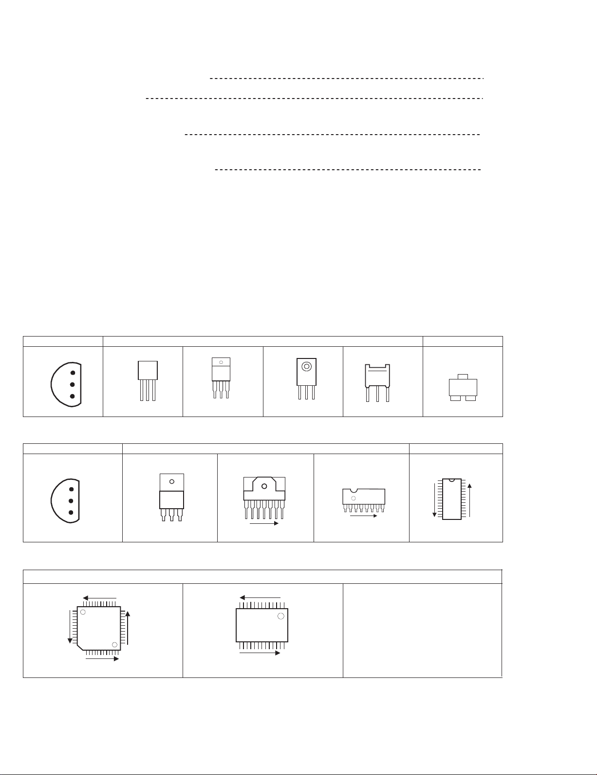
SEMICONDUCTOR SHAPES
BLOCK DIA GRAM
CIRCUIT DIAGRAMS
MAI N PWB CI RCUIT DIAGRA M
P ATTERN DIAGRAMS
MAIN PWB & CRT SOCKET PATTERN
SEMICONDUCTOR SHAPES
TRANSISTOR
BOTTOM VIEW
E
C
B
ECB
BCE
(G)(D)(S)
IC
B O TT OM VI EW F R O NT V IE W TO P VI EW
CHIP IC
2-2
OUT
E
IN
N
N
N
1
N
IN OUTE
FRONT VIEW
1 N
TO P VI EW
ECB
1
N
No.51924
TO P VI EW
CHIP TR
ECB
1 N
1
2-2
2-3
2-5
2-13
C
BE
N
Page 4

BLOCK DIAGRAM
Q102
IF AMP
SF101
VIDEO
AUDIO
IC701
MICRO COMPUTER
IC201
1 CHIP DECODER
RGB
10.11.12
29
30
38
24
MAIN PWB
IC702
MEMORY
IC651
AUDIO AMP
SP
AUDIO
3
8
OSD
RGB
SF102
SCL/SDA
B1
IC421
VERT.OUT
Q522
H.OUT
DY(V)
DY(H)
DEF.YOKE
H.OUT V.OUT
H.OUT
V.OUT
42
46
SCL
SDA
POWER SW
IN
OUT
AC IN
Q103
SW
HEAD
PHONE
CF901
30.31.32
SAW
EXT
RGB
TU001
TUNER
IF
T921
SW
TRANSF.
IC921
POWER
REG.
PC921
VOLTAGE
FEEDBACK
IC941
ERROR
AMP
IC971
5/9V REG.
REG.
D901
RECT
R / G /B
V01
CRT
CRT SOCKET
PWB
RGB
DRV
ECO
REMOCON
KEY
IND.
VIDEO
AUDIO
T522
HVT
FOCUS
SCREEN
EHV
B1
SP
18.19
3.58/
OTH
25
37.38
6.7.8
VIDEO
IN
VIDEO
OUT
AUDIO
IN
AUDIO
OUT
SCL
SDA
SP
OUT
VIDEO
AUDIO
REAR
FRONT
IN
AV-20N41
AV-16N71
AV-20N41
AV-16N71
No.51924
2-3 2-4
No.51924
Page 5

AV-20N41
AV-16N71
AV-20N41
AV-16N71
CIRCUIT DIAGRAMS MAIN PWB CIRCUIT DIAGRAM
(1/2) [AV-20N41]
AT24C08-21DTT2
MEMORY
MAIN PWB
SCG-1291A-BK
820
2W
.47/50
680p
No.51924 No.51924
2-5 2-6
Page 6

MAIN PWB CIRCUIT DIAGRAM (2/2) [AV-20N41]
AV-20N41
AV-16N71
AV-20N41
AV-16N71
QMPR010-200-E2
.1 AC275V MPP
.047 AC275V MPP
AC250V
AC250V
10W
AC250V
470p AC250V
470p AC250V
CRT SOCKET PWB
(Within MAIN PWB)
SCG-1291A-BK
(2/2)
A48KXR064X
PICTURE TUBE
.001
3KV
QCZ0121-102
.001 AC250V
MPP
.0096 1.5KVH
4.7K
.22 250V MPP
.27 250V MPP
114.5V
TP-91
( B1 )
1W
MAIN PWB
(1/2)
TP-E
( )
QFZ0200-962
680
1/2W
QQLZ034-500
QQH0073-001
2.2 1/4W
R582
27K 1/10W
NRSA02J-273X
No.51924
SCG-1291A-BK
2-7 2-8
QQD0034-001
No.51924
Page 7

MAIN PWB CIRCUIT DIAGRAM (1/2) [AV-16N71]
AV-20N41
AV-16N71
AT24C08-21DTT2
MEMORY
AV-20N41
AV-16N71
MAIN PWB
SCG-1297A-CK
2W
-H2
No.51924 No.51924
2-9 2-10
Page 8

MAIN PWB CIRCUIT DIAGRAM (2/2) [AV-16N71]
AV-20N41
AV-16N71
AV-20N41
AV-16N71
QAD0119
-9R0
QMP40D0-200J5
QAF0052-621
.047 AC275V
AC250V
.1
AC250V
QCZ9082-222Z
120/400
470p
AC250V
470p AC250V
AC250V
MPP
.0081 1.5KVH
QFZ0200-812
CRT SOCKET PWB
(Within MAIN PWB)
SCG-1297A-CK
(2/2)
A38JLL91X13
PICTURE TUBE
-H2
4.7 7W
.27 250V MPP
QFZ0199-274
.27 250V MPP
QFZ0199-274
1/2W
114.5V
-H2
.001 AC250V
TP-E
( )
1W
MAIN PWB
(1/2)
TP-91
( B1)
QQH0072-001
2.2 1/4W
27K 1/10W
No.51924
SCG-1297A-CK
2-11 2-12
(ITC)
No.51924
Page 9

AV-20N41
AV-16N71
AV-20N41
AV-16N71
PATTERN DIAGRAMS MAIN PWB & CRT SOKET PWB PATTERN
FRONT
MAIN PWB
TP-E
TP-91
(B1)
CRT SOCKET PWB
No.51924 No.51924
2-13 2-14
TOP
VP0111
DP6060
Page 10

VICTOR COMPANY OF JAPAN, LIMITED
HOME AV NETWORK BUSINESS UNIT. 12, 3-chome, Moriya-cho, Kanagawa-ku, Yokohama, Kanagawa-prefecture, 221-8528, Japan
AV20N41BK-BK #3
AV16N71VT-CK #3
Printed in Japan
VP 0111
DP6060
 Loading...