

JRC NSVS670 User Manual
NSVS670 Nov. 2004
Application
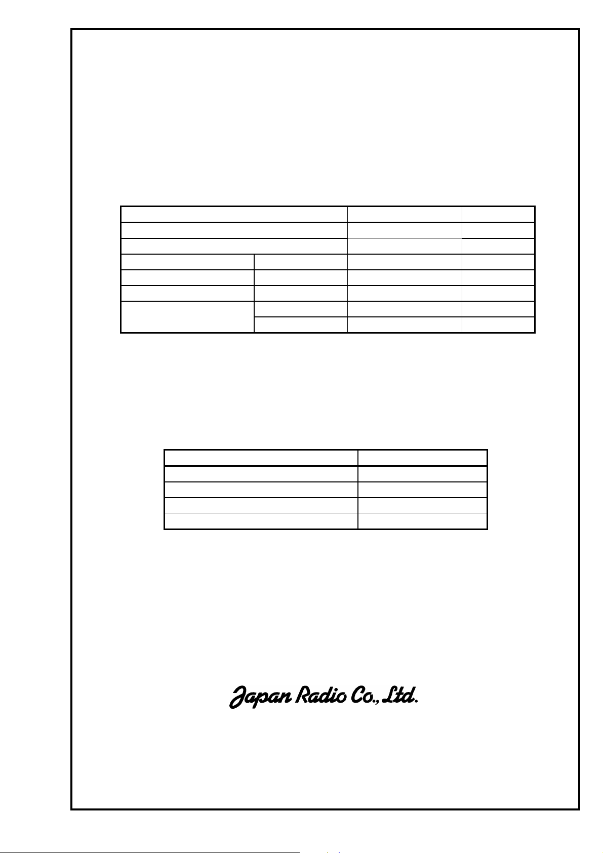
Electrical Specification: (Table 1)
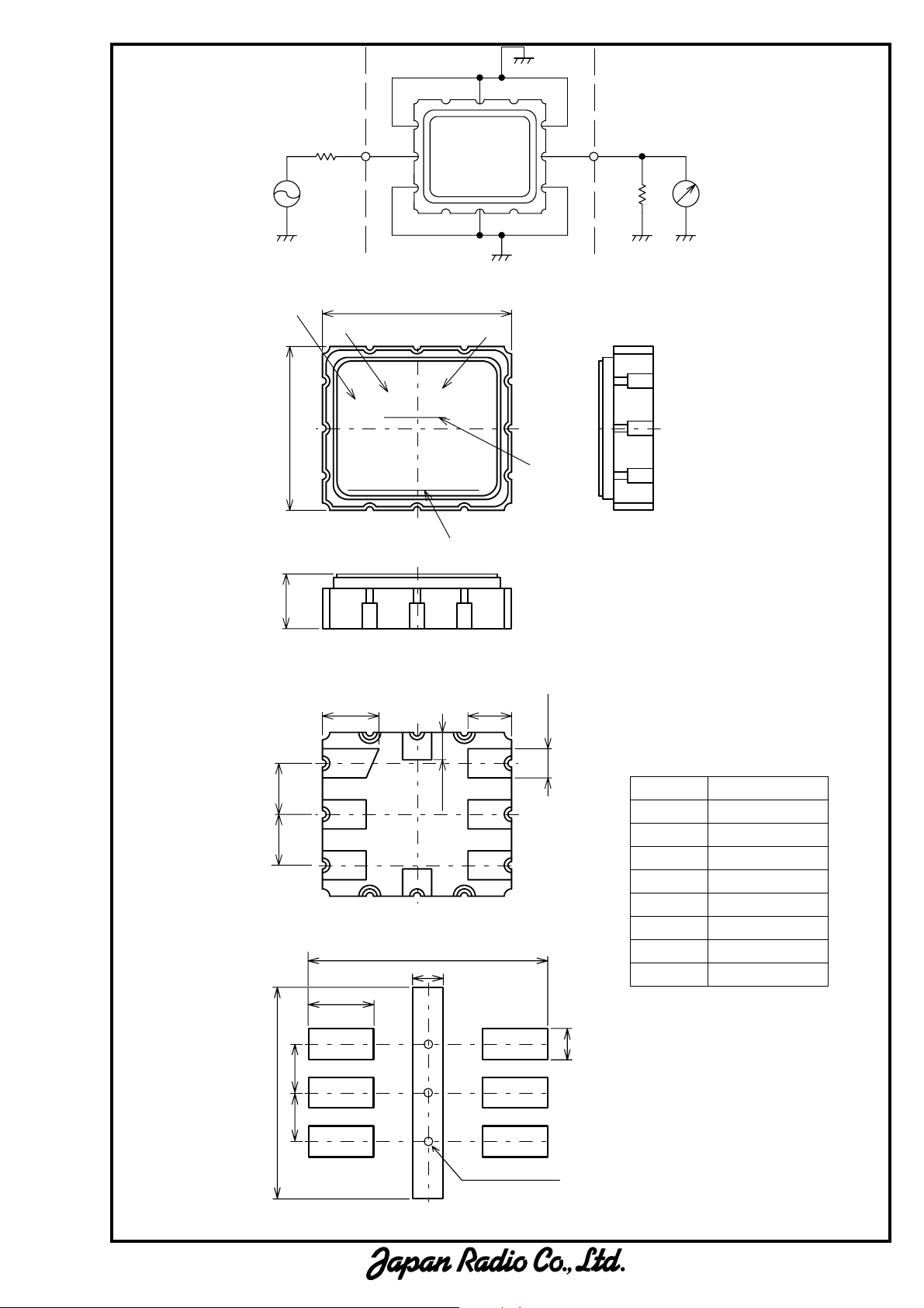
The device characteristics are measured in the circuit shown in Fig.1.
Maximum Rating: (Table 2)
Mechanical Specifications: (Fig.2)
Package is designed as small as 5.2x4.5x1.5[mm
Notice:
This part is electrostatic discharge sensitive and may be damaged by improper handling.
420MHz PAGER
Table 1. Electrical Specifications
Item Spec. Typ.
Input and Output Impedance
Nominal Center Frequency (f0) 420MHz −
Insertion Loss 410~430MHz 4.0dB max. 3.1dB
Response Variation 410~430MHz 2.0dB max. 0.9dB
Input and Output VSWR 410~430MHz 2.5 max. 1.7
(Relative to Through Level)
Table 2. Maximum Ratings
Item Rating
Maximum Input Power +20dBm
Maximum DC Voltage 7.5V
Operating Temperature Range -10~+60ºC
Storage Temperature -30~+85ºC
http://www.jrc.co.jp/jp/product/device/saw/index.html (Japanese)
JRC SAW FILTER
NSVS670
50Ω
380MHz 40dB min. 45dB Out of Band Rejection
500MHz 40dB min. 50dB
(Operating Temperature Range: -10~+60ºC)
3
] for SMD (Surface Mount Device) type.
Communications Equipment Division
Communications Equipment Marketing Department
10-1, Nishi-Shinjuku 6-chome, Shinjuku-ku,
Tokyo, 160-8328 Japan
Tel. +81 3-3348-3845
Fax. +81 3-3348-3935
http://www.jrc.co.jp/eng/product/saw/index.html(English)
−
NSVS670 Nov. 2004
IN
50Ω
8
1
SAW
2
7
6
OUT
50Ω
3
5
4
(1)
(a)
Fig.1 Measuring circuit
5.2±0.2
(b)
J36
4.5±0.2
420
(2)
4
8
6.0
1.0
(0.75)
(3)
[2×]
(1.2)
[5X]
5
6
7
Marking
(1) Manufacture’s Mark
(2) Lot Number
(a) Year
(b) Month
*Oct.--- X
Nov.--- Y
[8×]
(0.8)
Dec.--- Z
(3) Part number Mark
Pin no. Connection
1 GND
2 IN/OUT
3 GND
4 GND
5 GND
6 OUT/IN
7 GND
8 GND
1.5±0.2
(1.55)
3
(1.27)
2
(1.27)
1
Fig.2 Package dimensions (in mm)
1.6
[6x]
1.27
5.3
1.27
Via-Hole(Φ0.3)
[3x]
1.0
[6x]
Fig.3 Desirable land area (in mm)
 Loading...