

JRC NJG1704KC1 Datasheet
NJG1704KC1
800MHz BAND FRONT-END GaAs MMIC
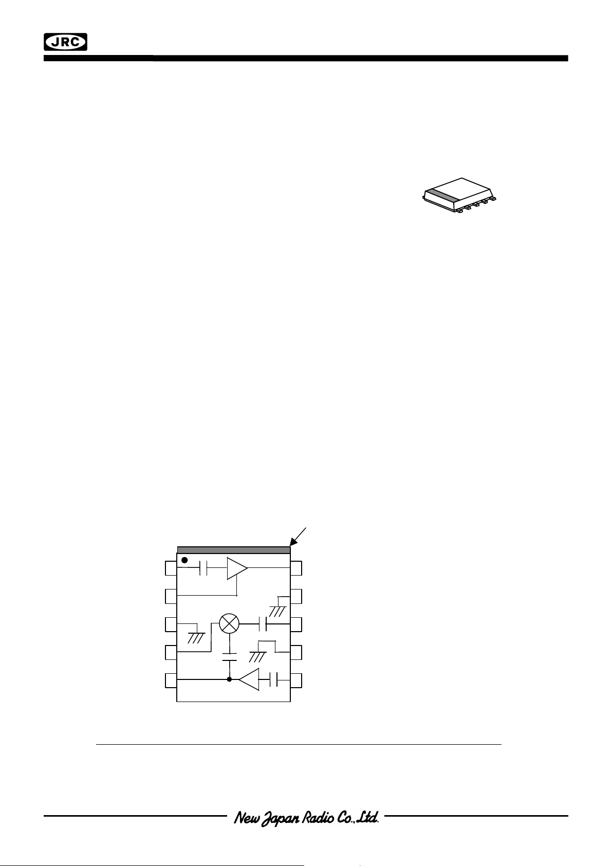
nGENERAL DESCRIPTION nPACKAGE OUTLINE
NJG1704KC1 is a front-end GaAs MMIC including
a LNA, a local amplifier and a mixer, designed mainly for
800MHz band cellular phone.
The ultra small & ultra thin FLP10-C1 package is applied.
NJG1704KC1
nFEATURES
lLow Voltage Operation +2.7V typ.
lLow Current Consumption LNA 3.1mA typ.
Mixer 6.1mA typ. (with local amplifier operation current)
lUltra Small & Ultra Thin package FLP10-C1 (Mount Size: 2.8 x 3.0 x 0.75mm)
n
LNA
lHigh Small Signal Gain 16.5dB typ. @ fRF=820MHz
lLow Noise Figure 1.4dB typ. @ fRF=820MHz
lHigh Input IP3 -4.0dBm typ. @ fRF=820.0+820.1MHz
n
Mixer
lHigh Conversion Gain 12.5dB typ. @ fRF=820MHz, fLO=690MHz, PLO=-10dBm
lLow Nose Figure 5.0dB typ. @ fRF=820MHz, fLO=690MHz, PLO=-10dBm
lHigh Input IP3 +1.0dBm typ. @fRF=820.0+820.1MHz, fLO=690MHz,PLO=-10dBm
nPIN CONFIGURATION
1
2
3
4
5 6
NOTE: Please note that any information on this catalog will be subject to change.
KC1 TYPE
(Top View)
Orientation Mark
10
9
8
7
Pin Connection
1.LNAIN
2.LNACAP
3.GND
4.IFOUT
5.VLO
6.LOIN
7.GND
8.MIXIN
9.GND
10.LNAOUT
- 1 -
NJG1704KC1
n
ABSOLUTE MAXIMUM RATINGS
(Ta=+25°C, Zs=Zl=50Ω)
PARAMETER SYMBOL CONDITIONS RATINGS UNITS
LNA Voltage V
Mixer Voltage V
LOCAL Amplifier Voltage V
Input Power 1 P
Input Power 2 P
Power Dissipation P
Operating Temperature T
Storage Temperature T
n
ELECTRICAL CHARACTERISTICS 1 (LNA)
GENERAL CONDITIONS: Ta=+25°C, V
LNA
MIX
LO
LNAIN
LOIN
D
opr
stg
V
LNA=VMIX=VLO
V
LNA=VMIX=VLO
=2.7V +15 dBm
=2.7V +10 dBm
=2.7V, V
LNA
MIX=VLO
PRF=-36dBm, Zs=Zl=50Ω, with test circuit
PARAMETER SYMBOL CONDITIONS MIN TYP MAX UNITS
Operating Frequency freq 800 820 900 MHz
LNA Voltage V
LNA Operating Current I
LNA
LNA
PRF, PLO=OFF - 3.1 3.7 mA
2.5 2.7 4.5 V
Small Signal Gain Gain 15.0 16.5 18.0 dB
Gain Flatness G
flat
fRF=810~885MHz - 0.5 1.0 dB
Noise Figure NF - 1.4 1.6 dB
Pout at 1dB Gain
Compression point
Input 3rd Order Intercept
point
RF IN VSWR VSWR
RF OUT VSWR VSWR
P
-1dB
-3.0 -1.0 - dBm
IIP3 fRF=820.0+820.1MHz -10.0 -4.0 - dBm
i
o
- 1.6 2.0
- 1.5 2.0
5.0 V
5.0 V
5.0 V
550 mW
-40~+85 °C
-55~+125 °C
=0V, fRF=820MHz
n
ELECTRICAL CHARACTERISTICS 2 (Mixer)
GENERAL CONDITIONS: Ta=+25°C, V
LNA
=0V, V
MIX=VLO
=2.7V, fRF=820MHz, fLO=690MHz
PRF=-30dBm, PLO=-10dBm, Zs=Zl=50Ω, with test circuit
PARAMETER SYMBOL CONDITIONS MIN TYP MAX UNITS
Operating Frequency freq 800 820 900 MHz
Mixer Voltage V
Local Amplifier Voltage V
Mixer Operating Current I
Local Amplifier Operating
Current
I
Conversion Gain G
MIX
MIX
LO
LO
PRF, PLO=OFF - 5.0 6.3 mA
PRF, PLO=OFF - 1.0 1.2 mA
c
2.5 2.7 4.5 V
2.5 2.7 4.5 V
11.0 12.5 - dB
Noise Figure NF - 5.0 7.0 dB
Input 3rd Order Intercept
Point
IIP3 fRF=820.0+820.1MHz - +1.0 - dBm
- 2 -
n
TERMINAL INFORMATION
No. SYMBOL FUNCTION
1 LNAIN RF input terminal of LNA. An external matching circuit is required.
2 LNACAP
3 GND Ground terminal(0V)
4 IFOUT
5 VLO
6 LOIN
NJG1704KC1
Terminal for the bypass capacitor of LNA. The bypass capacitor C1 as
shown in test circuits, should be connected to this terminal as close as
possible.
IF signal output terminal. The IF signal is output through external matching
circuit connected to this terminal. Please connect inductances L7, L8 and
power supply as shown in test circuits, since this terminal is also the
terminal of mixer power supply.
Power supply terminal for local amplifier. Please place R1 and L10 as
shown in test circuits at very close to this terminal.
Local signal input terminal to local amplifier. An external matching circuit is
required.
7 GND Ground terminal(0V)
8 MIXIN RF signal input terminal to mixer. An external matching circuit is required.
9 GND Ground terminal(0V)
Signal output terminal of LNA. The RF signal from LNA is output through
10 LNAOUT
CAUTION
1) Ground terminal (No.3, 7, 9) should be connected to the ground plane as low
inductance as possible.
external matching circuit connected to this terminal. Please connect
inductances L3, L4 and power supply as shown in test circuits, since this
terminal is also the terminal of LNA power supply.
- 3 -
NJG1704KC1
n
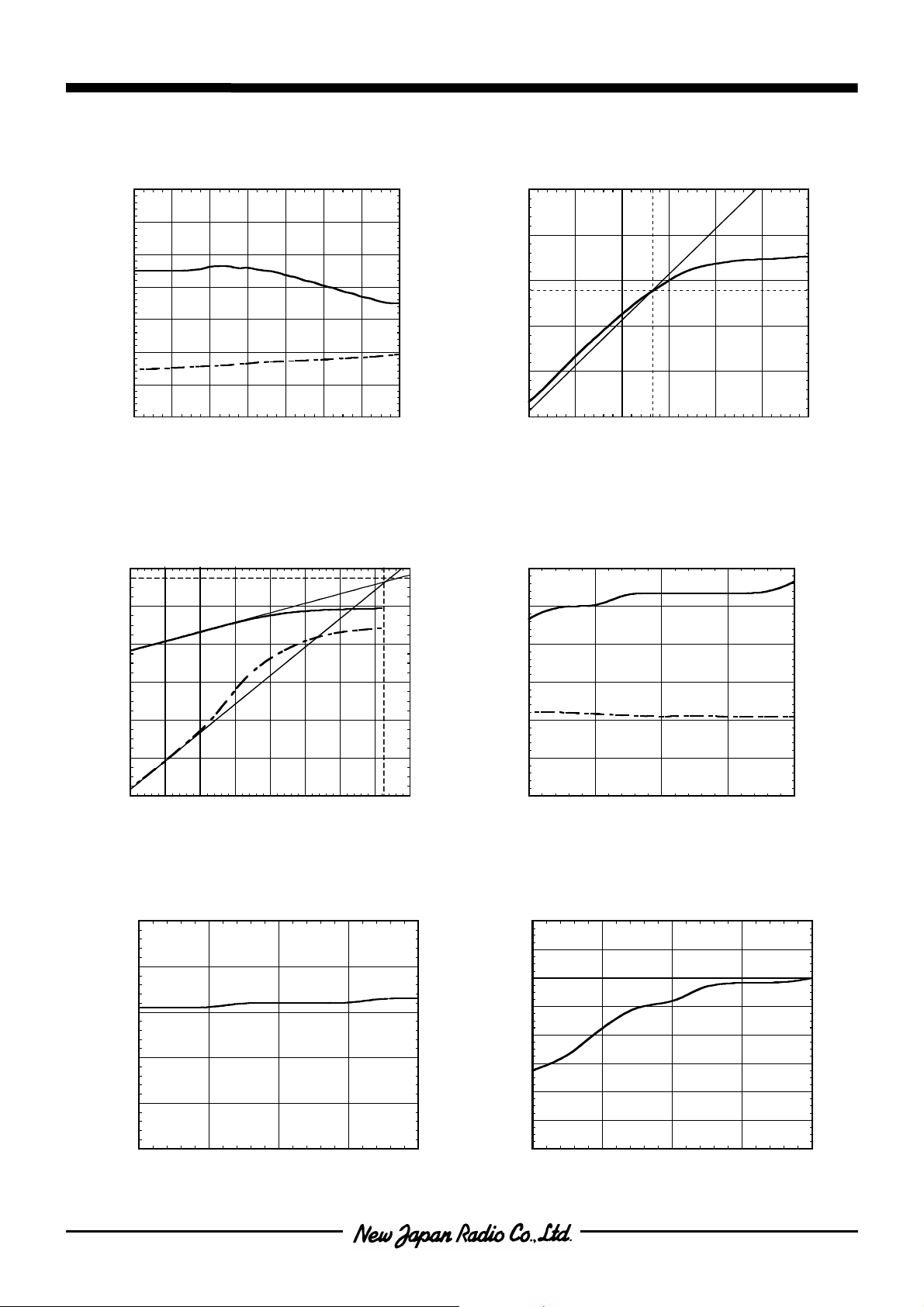
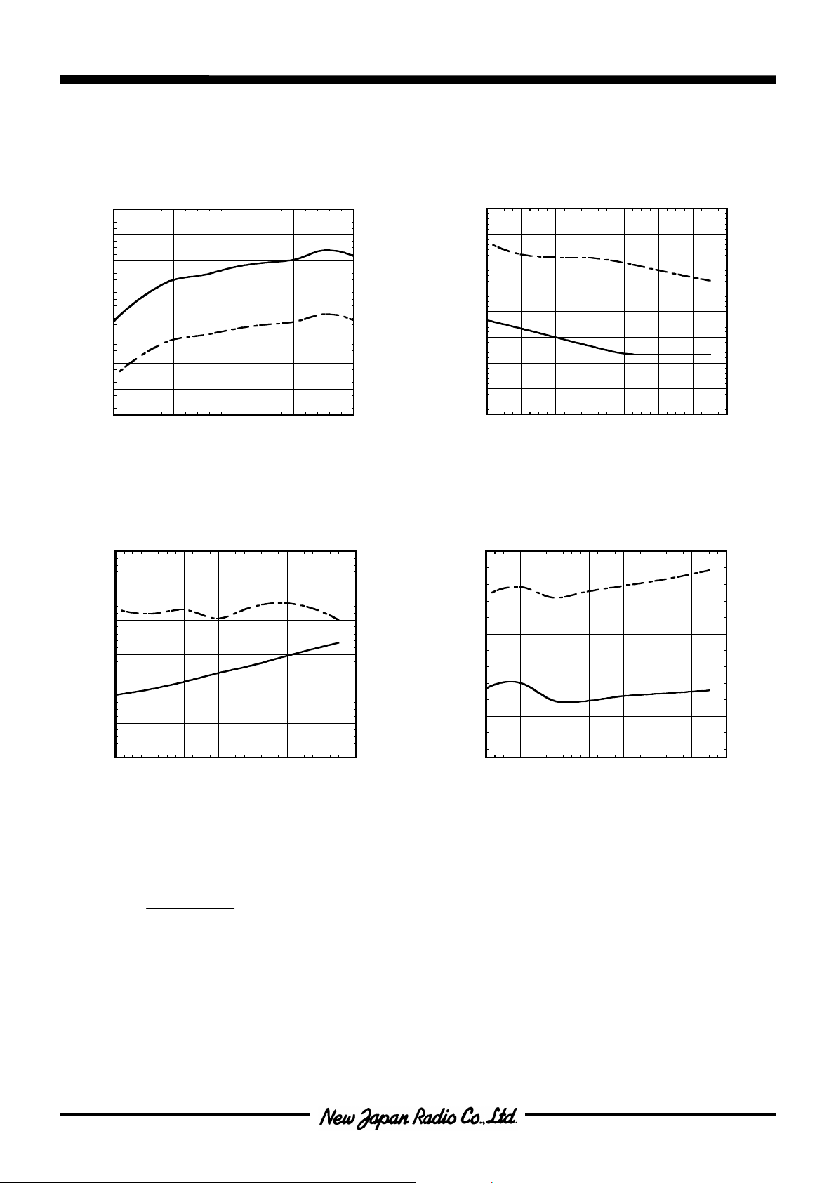
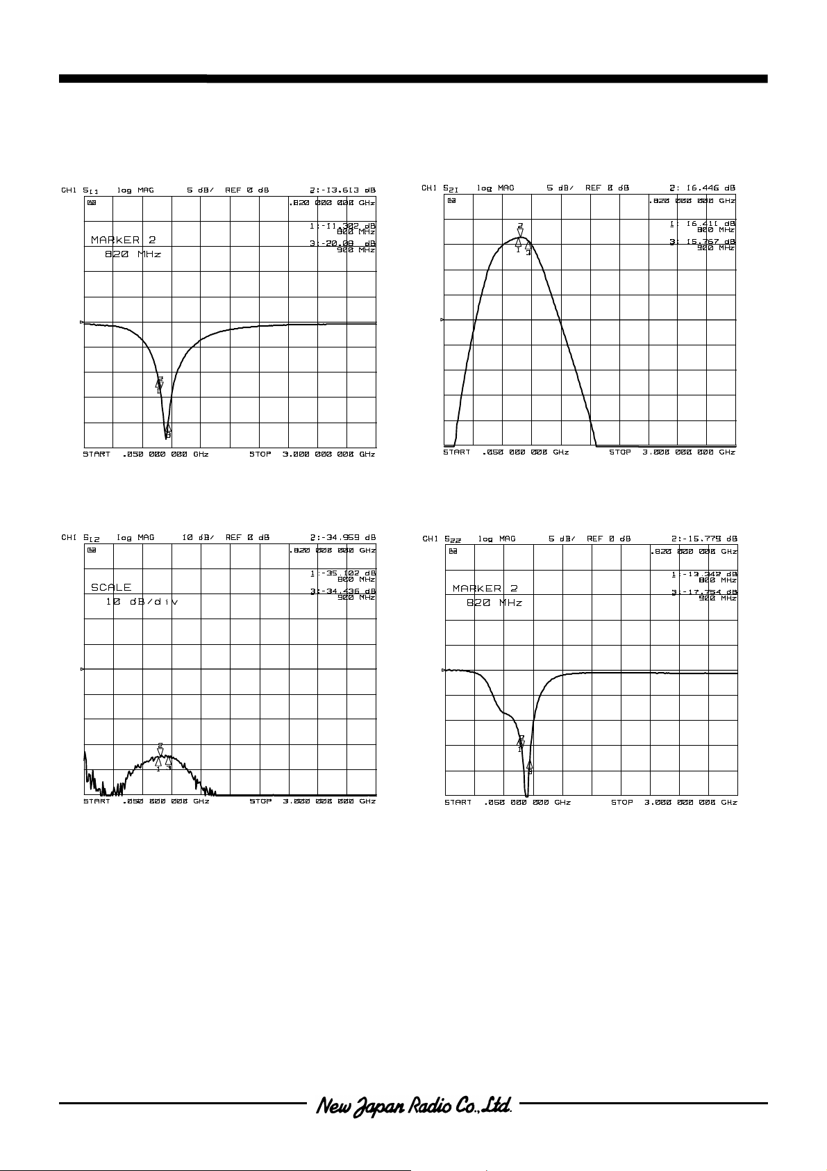
TYPICAL CHARACTERISTICS (LNA,fLO=690MHz,with test circuit)
Gain,Noise Figure vs. Frequency
(V
=2.7V)
19
18
17
Gain
16
15
Gain (dB)
14
13
12
780 800 820 840 860 880 900 920
LNA
Frequency (MHz)
Pout,IM3 vs. Pin
(V
=2.7V,f=820.0+820.1MHz)
20
0
LNA
Pout vs. Pin
(V
=2.7V,f=820MHz)
4
3.5
3
2.5
2
NF
Noise Figure (dB)
1.5
1
0.5
10
5
0
-5
Pout (dBm)
-10
-15
-30 -25 -20 -15 -10 -5 0
17
Gain
16.5
LNA
P-1dB
-1.1dBm
Pin (dBm)
Gain,Noise Figure vs. V
(f=820MHz)
LNA
2
-20
-40
Pout,IM3(dBm)
-60
-80
-100
-40 -35 -30 -25 -20 -15 -10 -5 0
3.3
3.2
3.1
(mA)
LNA
I
2.9
Pout
IM3
Pin (dBm)
I
vs. V
LNA
3
IIP3
-3.6dBm
LNA
16
15.5
Gain (dB)
15
14.5
14
2.5 3 3.5 4 4.5
V
(V)
LNA
P-1dB vs. V
LNA
(f=820MHz)
8
6
4
2
0
-2
P-1dB (dBm)
-4
-6
1.5
NF
Noise Figure (dB)
1
- 4 -
2.8
2.5 3 3.5 4 4.5
V
(V)
LNA
-8
2.5 3 3.5 4 4.5
V
(V)
LNA
n
TYPICAL CHARACTERISTICS (LNA, fLO=690MHz,with test circuit)
NJG1704KC1
OIP3,IIP3 vs. V
LNA
(f=820.0+820.1MHz,Pin=-36dBm)
20
18
16
14
12
OIP3 (dBm)
10
8
6
4
2.5 3 3.5 4 4.5
OIP3
IIP3
V
(V)
LNA
Noise Figure,P-1dB vs. Temperature
(V
=2.7V,f=820MHz)
3
LNA
8
6
4
2
0
-2
-4
-6
-8
0
IIP3 (dBm)
Gain,I
19
18.5
18
17.5
17
Gain (dB)
16.5
16
15.5
15
-40 -20 0 20 40 60 80 100
Gain
vs. Temperature
LNA
(V
=2.7V,f=820MHz)
LNA
I
LNA
Ambient Temperature (oC)
OIP3,IIP3 vs. Temperature
(V
=2.7V,f=820.0+820.1MHz,Pin=-36dBm)
LNA
16
3.3
3.2
3.1
3
2.9
2.8
2.7
2.6
2.5
-3
(mA)
LNA
I
2.5
2
1.5
NF
1
Noise Figure (dB)
0.5
0
-40 -20 0 20 40 60 80 100
Ambient Temperature (oC)
P-1dB
The value of OIP3 and IIP3 shown in
typical characteristics are calculated
OIP3=
3 x Pout-IM3
2
IIP3=OIP3-Gain @Pin=-36dBm
-1
-2
-3
-4
-5
-6
P-1dB (dBm)
15
14
13
OIP3 (dBm)
12
11
-40 -20 0 20 40 60 80 100
OIP3
Ambient Temperature (oC)
IIP3
-4
-5
-6
-7
-8
IIP3 (dBm)
- 5 -
NJG1704KC1
n
TYPICAL CHARACTERISTICS (LNA, fLO=690MHz,with test circuit)
S11
S12
Condition
V
=2.7V
LNA
V
MIX=VLO
S21
S22
=0V
- 6 -
 Loading...