

JRC NJG1701V Datasheet
NJG1701V
PHS MULTI-FUNCTION GaAs MMIC
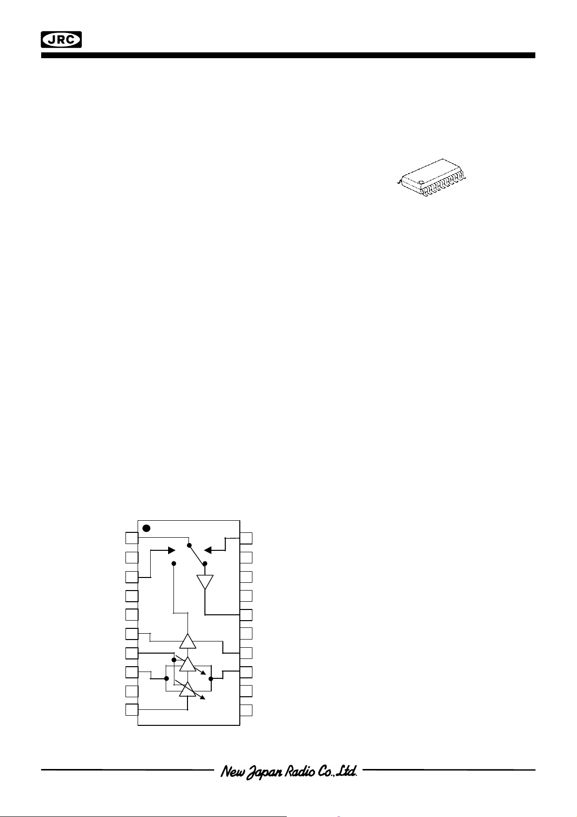
Pin Connection
NJG1701V
n
GENERAL DESCRIPTION
NJG1701V is a GaAs multi-function MMIC composed of a
power amplifier, a SPDT switch and a LNA for Japanese PHS
or WLL application. The SSOP20 package is adopted and
effective for downsizing of handsets.
NJG1701V is operated at low voltage with low current and
low distortion PA, low loss switch and low noise and high gain
LNA.
n
APPLICATION
l
PHS, Digital cordless phone
n
FEATURES
(Operating frequency f=1.9GHz)
Transmitting Mode Operation
l
Drain Voltage (PA) 3.0V typ.
l
Gain 32dB typ.
l
Current consumption 160mA typ. @P
l
Gain variable range 33dB typ.
Receiving Mode Operation
l
Drain Voltage (LNA) 3.0 typ.
l
Gain 14dB typ.
l
Current consumption 2.8mA typ.
l
NF 2.7dB typ.
l
Control Voltage (SW) 2.7V typ.
l
Package SSOP20 (Mount Size: 6.4x6.5x1.25mm)
=20dBm
OUT
n
PACKAGE OUTLINE
n
PIN CONFIGURATION
10
V Type
(Top View)
1
2
3
20
19
18
1.ANT 11.GND
2.GND 12.GND
4
5
6
7
8
9
17
16
15
14
13
12
11
3.V
SW2
4.GND 14.V
5.V
DD1
6.V
GG1
7.V
CONT
8.V
GG2
13.V
DD3
DD2
15.GND
16.LNAOUT
17.GND
18.EXTIND
9.GND 19.GND
10.PA
20.V
IN
SW1
NJG1701V
n
DD1
SW1
SW2
ABSOLUTE MAXIMUM RATINGS
PARAMETER SYMBOL CONDITIONS RATINGS UNITS
(Zs=Zl=50Ω, Ta=25°C)
Drain Voltage1 V
Drain Voltage2 V
Gate Voltage V
Gain Control Voltage V
Control Voltage V
Input Power1 ANT V
Input Power2 PA
Power Dissipation P
Operating Temp. T
Storage Temp. T
n
ELECTRICAL CHARACTERISTICS 1 (TRANSMITTING MODE: PAin–ANT)
(f=1.90GHz, V
DD1
DD2,3
GG1,2
cont
SW1,2
in
D
opr
stg
V
=-0.9V 6.0 V
GG1,2
V
=3.0V -4.0 V
DD2,3
V
=3.0V -4.0 V
DD2,3
V
DD2,3
=3.0V, V
=3.0V, V
=0V, V
=-0.9V 3 dBm
GG1,2
=2.7V 0 dBm
At on PCB board 800 mW
=2.7V, V
SW1
SW2
=0V, V
=0V, Zs=Zl=50Ω, V
CONT
PARAMETER SYMBOL CONDITIONS MIN TYP MAX UNITS
Operating frequency freq V
Drain voltage V
Gate voltage V
Idle current *1 I
DD2,3
GG1,2
idle
=3.0V 1.89 1.90 1.92 GHz
DD2,3
V
=3.0V, I
DD2,3
V
=3.0V, No RF Signal -1.3 -0.9 -0.5 V
DD2,3
P
=20dBm, V
out
=150mA 2.9 3.0 5.2 V
idle
=3.0V 145 150 155 mA
DD2,3
6.0 V
6.0 V
-30~+85 °C
-40~+150 °C
=0V, Ta=25°C)
DD1
Operating current *1 I
Gate current *2 I
Gain control terminal
current
Gain control voltage V
Control voltage1 V
Control voltage2 V
Control current I
DD2,3
GG
I
CONT
CONT
SW1
SW2
SW1
Small signal gain Gain1 V
Gain flatness G
Gain control range G
Pout at 1dB gain
compression point
Adjacent Channel
Leakage Power 1
Adjacent Channel
Leakage Power 2
CONT
P
P
P
flat1
-1dB
acp1
acp2
P
=20dBm, V
out
P
=20dBm, V
out
-2.0<V
P
=20dBm, V
out
P
=20dBm, V
out
P
=20dBm, V
out
V
DD2,3
DD2,3
V
DD2,3
-2.0V<V
V
DD2,3
P
=20dBm, offset=600kHz,
out
I
=150mA
idle
<0.0V -5.0 -2.0 0.0 uA
CONT
=3.0V, I
=3.0V, I
=3.0V, I
<0.0V 29 33 37 dB
CONT
=3.0V, I
Pin=π/4 QPSK, V
P
=20dBm, offset=900kHz,
out
I
=150mA,
idle
Pin=π/4 QPSK, V
=3.0V 145 160 175 mA
DD2,3
=3.0V -50.0 -10.0 0.0 uA
DD2,3
=3.0V -2.0 0.0 0.0 V
DD2,3
=3.0V 2.5 2.7 5.2 V
DD2,3
=3.0V -0.2 0.0 0.2 V
DD2,3
=150mA - 4.0 12.0 uA
idle
=150mA 29 32 35 dB
idle
=150mA - 0.5 1.0 dB
idle
=150mA 20 22 - dBm
idle
DD2,3
DD2,3
- -60 -55 dBc
=3.0V
- -65 -60 dBc
=3.0V
NJG1701V
PARAMETER SYMBOL CONDITIONS MIN TYP MAX UNITS
out
DD2,3
P
=20dBm, V
Harmonics P
PA
Port VSWR VSWR1 V
in
ANT-LNAOUT
Isolation
ANT Port Load VSWR
Tolerance
Switching time T
n
ELECTRICAL CHARACTERISTICS 2 (RECEIVING MODE; ANT - LNAOUT)
hm
I
SL
-
SW1
(f=1.90GHz, V
out
I
=150mA
idle
=3.0V, I
DD2,3
V
=0V,V
DD1
V
SW2
P
=20dBm, V
I
=150mA
idle
SW1
=0V
Load VSWR=4:1,
All phase
SW1
=0V, V
=2.7V, Zs=Zl=50Ω, V
SW2
=3.0V
DD2,3
=150mA - 1.7 2.2
idle
=2.7V,
=3.0V,
- -40 -30 dBc
35 40 - dB
Parasitic Oscillation for
Fundamental Signal Level
<
: -60dBc
=
- 15 - nS
DD2,3=VGG1,2=VCONT
PARAMETER SYMBOL CONDITIONS MIN TYP MAX UNITS
=0V, Ta=25°C)
Operating frequency freq V
Drain Voltage V
Operating current *3 I
Control voltage1 V
Control voltage2 V
Control current I
DD1
DD1
SW1
SW2
SW2
Small signal gain Gain2 V
Gain flatness G
flat2
Noise figure NF V
ANT Port VSWR VSWR2 V
LNAOUT Port VSWR VSWR3 V
Output 3rd
Intercept Point
Switching time T
*1: Total current of V
*2: Total current of V
*3: Current of V
terminal.
DD1
DD2
GG1
OIP3 V
SW2
and V
DD3
and V
GG2
DD1
V
DD1
DD1
V
DD1
DD1
DD1
DD1
DD1
terminal.
terminal.
=3.0V 1.89 1.90 1.92 GHz
2.7 3.0 5.2 V
=3.0V 2 2.8 4.2 mA
-0.2 0.0 0.2 V
2.5 2.7 5.2
- 4.0 12.0 µA
=3.0V 12 13 16 dB
=3.0V - 0.5 1.0 dB
=3.0V - 2.7 3.3 dB
=3.0V - 1.7 2.2
=3.0V - 2.0 2.5
=3.0V -10 0 - dBm
- 15 - nS
- 3-
NJG1701V
n
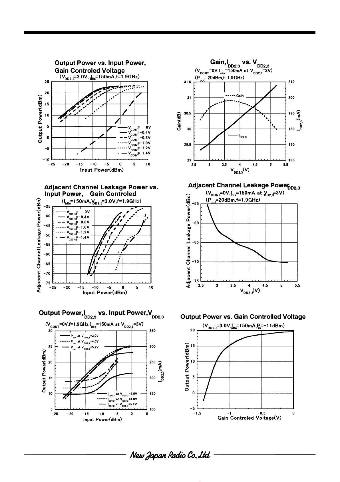
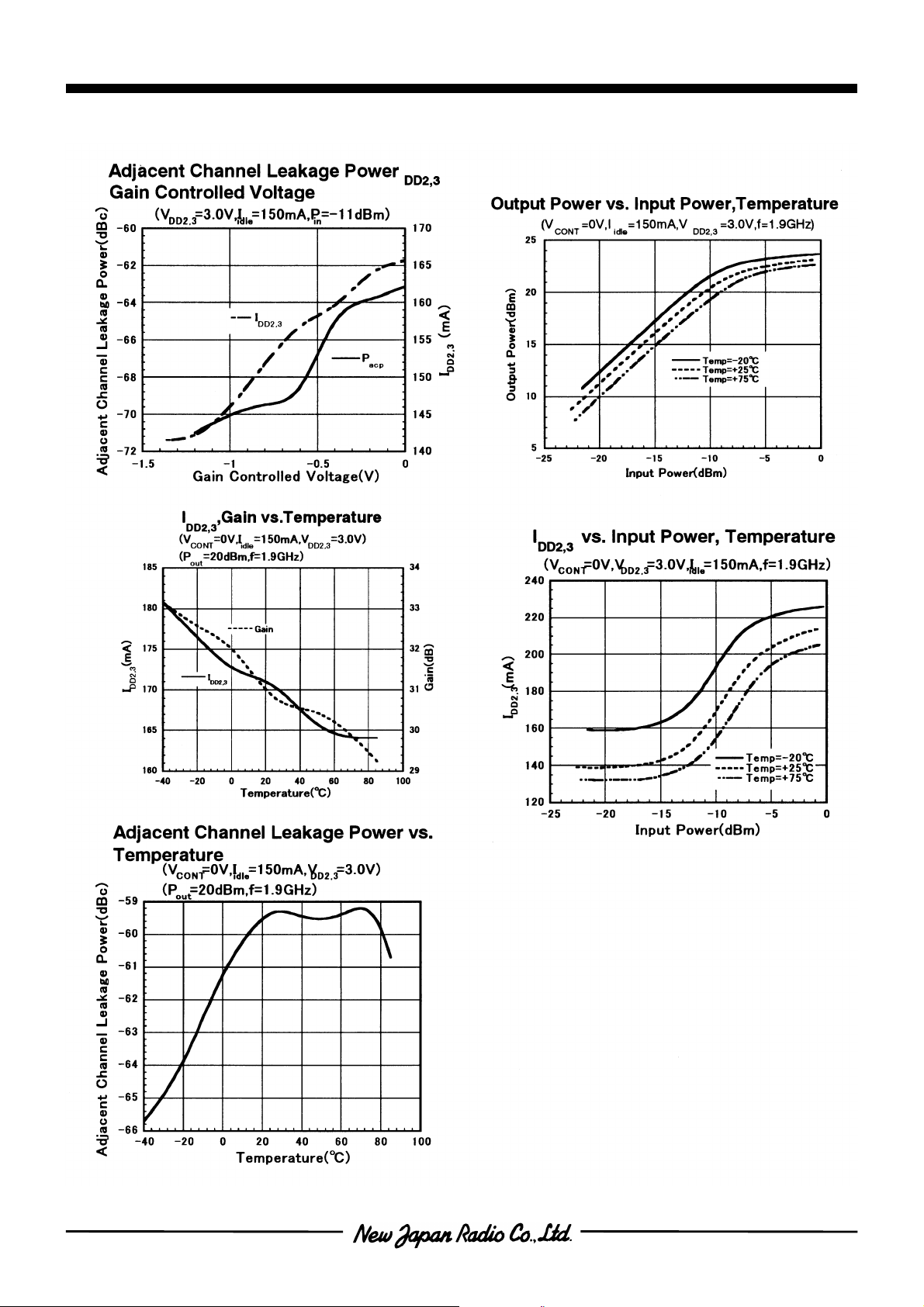
TYPICAL CHARACTERISTICS
TRANSMITTING MODE
NJG1701V
n
TYPICAL CHARACTERISTICS
TRANSMITTING MODE
- 5-
 Loading...