


NJG1557KB2
- 1 -
800MHz BAND MIXER GaAs MMIC
n
GENERAL DESCRIPTION
n
PACKAGE OUTLINE
NJG1557KB2 is a GaAs MMIC MIXER IC with built-in
local amplifier for 800MHz cellular phone handsets.
This mixer features very high input IP3, high conversion
gain and low noise figure, and suitable for the application
which needs high input IP3 such as CDMA.
An ultra small & ultra thin FLP6-B2 package is adopted.
n
FEATURES
l
Low voltage operation +2.8V typ.
l
Low current consumption 8.7mA typ.
l
High input IP3 +8dBm typ. @fRF=850.0+850.1MHz, PRF=-25dBm
fLO=740MHz, PLO=-10dBm
l
High conversion gain 9.5dB typ. @fRF=850MHz, PRF=-25dBm
fLO=740MHz, PLO=-10dBm, fIF=110MHz
l
Low noise figure 5.5dB typ. @fRF=850MHz
fLO=740MHz, PLO=-10dBm, fIF=110MHz
l
Ultra small & ultra thin package FLP6-B2 (Mount Size: 2.1x2.0x0.75mm)
n
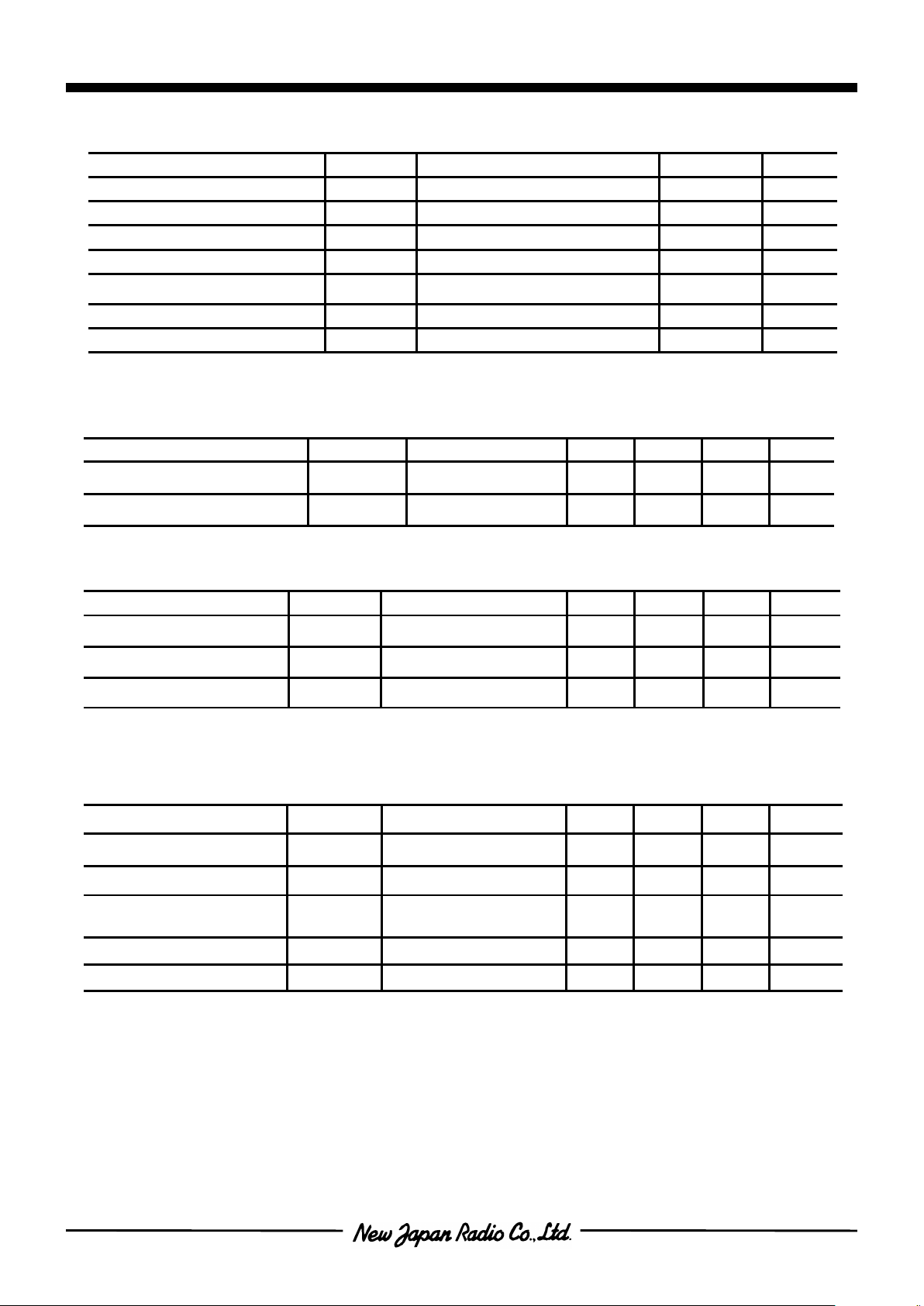
PIN CONFIGURATION
NJG1557KB2
KB2 Type
(Top View)
1
2
3
5
4
6
NOTE: The portion above shows orientation mark printed on the package surface.
Pin Connection
1. LOIN
2. GND
3. RFIN
4. IFOUT
5. SOURCE
6. VLO
NOTE: Please note that any information on this catalog will be subject to change.
NJG1557KB2
- 2 -
n
ABSOLUTE MAXIMUM RATINGS
(Ta=+25°C, Zs=Zl=50Ω)
PARAMETER SYMBOL CONDITIONS RATINGS UNITS
Mixer Supply Voltage V
MIX
6.0 V
Local Amp. Supply Voltage V
LO
6.0 V
Mixer RF Input Power P
RFIN
V
MIX=VLO
=2.8V +10 dBm
Mixer LO Input Power P
LOIN
V
MIX=VLO
=2.8V +10 dBm
Power Dissipation P
D
450 mW
Operating Temperature T
opr
-40~+85 °C
Storage Temperature T
stg
-55~+125 °C
n
RECOMMENDED OPERATING RANGE
PARAMETER SYMBOL CONDITIONS MIN TYP MAX UNITS
Supply Voltage Mixer V
MIX
2.7 2.8 5.5 V
Supply Voltage Local Amp. V
LO
2.7 2.8 5.5 V
n
ELECTRICAL CHARACTERISTICS [DC CHARACTERISTICS]
PARAMETER SYMBOL CONDITIONS MIN TYP MAX UNITS
Total Operating Current I
TOTAL
I
MIX+ILO
- 8.7 10.6 mA
Mixer Current I
MIX
PRF=OFF, PLO=OFF - 7.5 9.3 mA
Local Amp. Current I
LO
PRF=OFF, PLO=OFF - 1.2 1.6 mA
n
ELECTRICAL CHARACTERISTICS [AC CHARACTERISTICS]
(V
MIX=VLO
=2.8V, fRF=850MHz, fLO=740MHz, fIF=110MHz, PRF=-25dBm, PLO=-10dBm, Ta=+25°C,
Zs=ZI=50Ω, Measuring Test Circuit)
PARAMETER SYMBOL CONDITIONS MIN TYP MAX UNITS
Operating RF Frequency f
RF
830 850 900 MHz
Conversion Gain Gc 8.5 9.5 - dB
Input 3rd Order
Intercept Point
IIP3 fRF=850.0+850.1MHz +6.0 +8.0 - dBm
Noise Figure NF SSB - 5.5 6.5 dB
LO to RF Isolation ISL PRF=OFF 2.0 7.0 - dB
NJG1557KB2
- 3 -
n
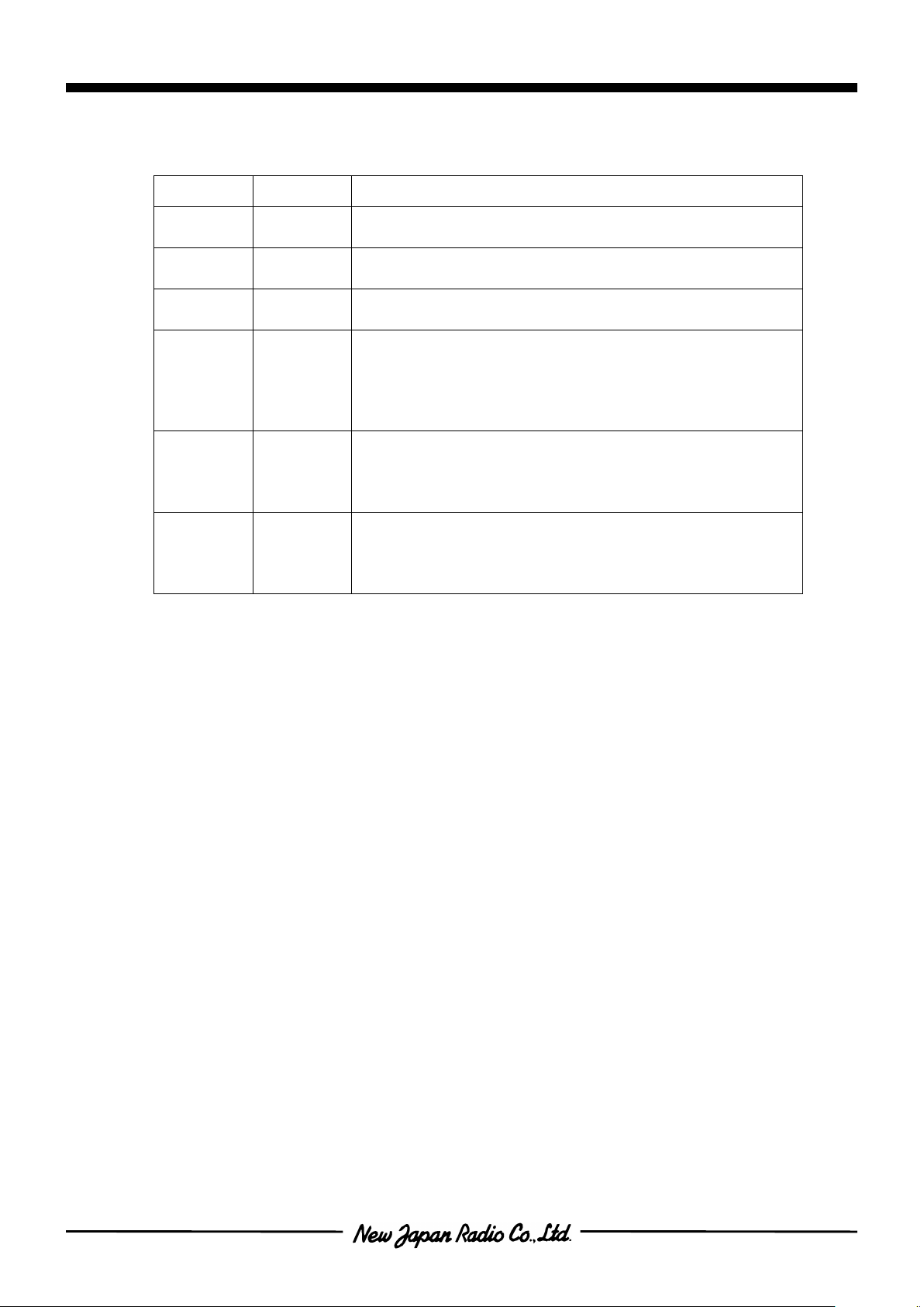
TERMINAL EXPLANATION
PIN No. SYMBOL DESCRIPTIONS
1 LOIN
Local power input terminal of local amplifier.
External matching circuit is required.
2 GND
Ground terminal (0V).
Please place grounding VIAs as close as possible.
3 RFIN
RF signal input terminal of mixer.
External matching circuit is required.
4 IFOUT
IF signal output terminal of mixer.
External matching circuit is required.
Please connect mixer power supply through inductor
(L7,L8) as shown in test circuit.
Please place bypass capacitor (C5) close to C4
5 SOURCE
Source terminal of mixer FET.
Please connect source inductor (L6), bias resistor (R2)
and bypass capacitor (C3) as shown in test circuit.
These parts should be placed close to this terminal.
6 VLO
Local amplifier power supply terminal.
Please place R1 and L5 close to this terminal as shown in
test circuit, and place bypass capacitors (C1,C2) close to
L5.
 Loading...