

NJG1555KB2
03/22/2000 Ver.5
NOTE: Please note that any information on this catalog will be subject to change.
NOTE: The portion above shows orientation mark printed on the package surface.
1
2
KB2 Type
TENTATIVE
800MHz BAND MIXER GaAs MMIC
n
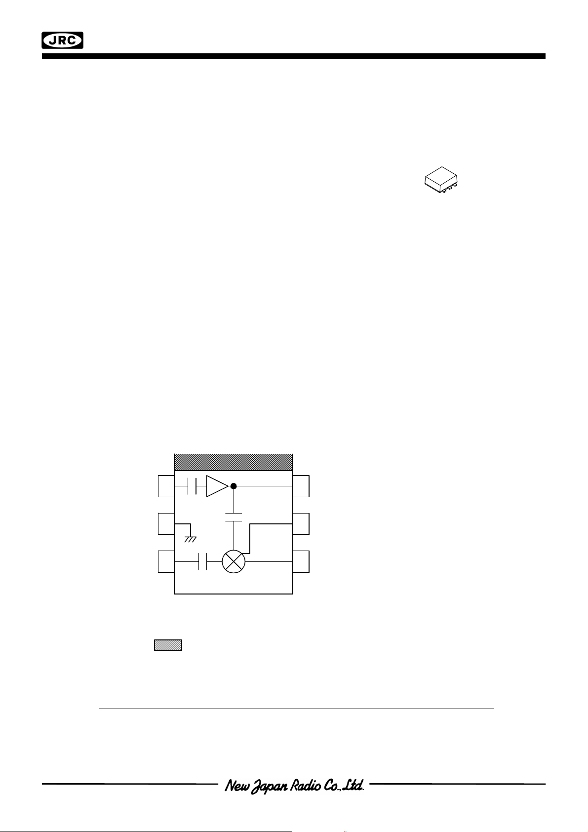
GENERAL DESCRIPTION
NJG1555KB2 is a mixer GaAs MMIC features low
distortion, high conversion gain and low noise figure.
NJG1555KB2 includes a mixer and a local amplifier,
and ideally suitable for 800MHz band digital mobile
phone handsets.
An ultra small & ultra thin FLP6-B2 package is adopted.
n
FEATURES
lLow voltage operation +2.7V
lHigh conversion gain 12dB typ. @fRF=820MHz, PLO=-15dBm
lHigh Input IP3 +1dBm typ. @fRF=820.0+820.1MHz, PLO=-15dBm
lLow noise figure 5dB typ. @fRF=820MHz, PLO=-15dBm
lUltra small & ultra thin package FLP6-B2 (Mount Size: 2.1x2.0x0.75mm)
n
PACKAGE OUTLINE
NJG1555KB2
n
PIN CONFIGURATION
(Top View)
3 4
Pin Connection
6
5
1. LOIN
2. GND
3. RFIN
4. IFOUT
5. BPC
6. VLO
- 1 -
NJG1555KB2
n
ABSOLUTE MAXIMUM RATINGS
(Ta=25°C, Zs=Zl=50Ω)
PARAMETERS SYMBOL CONDITIONS RATINGS UNITS
Mixer Supply Voltage V
Local Amplifier Supply
Voltage
Mixer RF Input Power P
Mixer LO Input Power P
Power Dissipation P
Operating Temperature T
Storage Temperature T
n
ELECTRICAL CHARACTERISTICS
GENERAL CONDITIONS: Ta=25°C, V
V
MIX
LO
RFIN
LOIN
D
opr
stg
V
=2.7V, VLO=2.7V 10 dBm
MIX
V
=2.7V, VLO=2.7V 10 dBm
MIX
=2.7V, VLO=2.7V, fRF=820MHz, fLO=690MHz
MIX
5 V
5 V
450 mW
-40~+85 °C
-55~+125 °C
PRF=-30dBm, PLO=-15dBm, Zs=Zl=50Ω, with test circuit
PARAMETERS SYMBOL CONDITIONS MIN TYP MAX UNITS
Operating Frequency freq 800 820 900 MHz
Mixer Supply Voltage V
Local Amplifier Supply
Voltage
Mixer Current I
Local Amplifier
Current
MIX
V
LO
MIX
I
LO
PRF=OFF, PLO=OFF - 5.0 7.0 mA
PRF=OFF, PLO=OFF - 1.0 1.6 mA
2.5 2.7 4.5 V
2.5 2.7 4.5 V
Conversion Gain G
Input 3rd Order
Intercept point
IIP3 fRF=820.0MHz+820.1MHz -1.0 +1.0 - dBm
C
10.0 12.0 - dB
Noise Figure NF - 5.0 6.0 dB
LO to RF Isolation ISL
IF OUT Port : 50Ω term.
- 9.0 - dB
- 2 -

NJG1555KB2
n
TERMINAL INFORMATION
PIN No. SYMBOL DESCRIPTIONS
1 LOIN
2 GND Ground terminal (0V).
3 RFIN RF input terminal of mixer. External matching circuit is required.
4 IFOUT
5 BPC
6 VLO
NOTE:
1) Ground terminal (2pin) should be connected with ground plane by multiple via holes
for good grounding.
Local power input terminal of local amplifier.
External matching circuit is required.
IF signal output terminal for mixer external matching circuit is required.
Please connect mixer power supply through choke inductor (L6) as shown in
test circuit.
Optional bypass capacitor terminal for mixer.
Please connect optimum capacitor if need for tuning Gc or IP3.
Local amplifier supply terminal.
Please place R1 & L4 close to this terminal as shown in test circuit.
- 3 -

NJG1555KB2
n
V
=V
=2.7V
TYPICAL CHARACTERISTICS (fLO=690MHz)
Conversion Gain , Noise Figure
vs. LO Power
14
12
10
8
6
Conversion Gain (dB)
4
2
-40 -30 -20 -10 0 10
Gc
NF
LO Power (dBm)
Condition
fIF=130MHz
fRF=820MHz, PRF=-30dBm
fLO=690MHz
V
MIX=VLO
=2.7V
14
12
10
8
6
Noise Figure (dB)
4
2
Output IP3 , Input IP3
vs. LO Power
16
14
12
10
8
6
OIP3 (dBm)
4
2
0
-40 -30 -20 -10 0 10
Condition
fIF=130MHz
fRF=820.0+820.1MHz
PRF=-30dBm
fLO=690MHz
OIP3
LO Power (dBm)
IIP3
3xIF-IM3
OIP3=
IIP3=OIP3-Gc
4
3
2
1
0
-1
IIP3 (dBm)
-2
-3
-4
2
IF Output Power vs. RF Power
5
0
-5
-10
-15
-20
IF Output Power (dBm)
-25
-30
-40 -35 -30 -25 -20 -15 -10 -5 0
RF Power (dBm)
Condition
fIF=130MHz
fRF=820MHz
fLO=690MHz, PLO=-15dBm
V
MIX=VLO
=2.7V
IF , IM3 vs. RF Power
20
0
IF
-20
-40
-60
IF , IM3 (dBm)
IM3
-80
-100
-40 -35 -30 -25 -20 -15 -10 -5 0
RF Power (dBm)
Condition
fIF=130MHz
fRF=820.0+820.1MHz
fLO=690MHz, PLO=-15dBm
V
MIX=VLO
=2.7V
- 4 -
 Loading...