

Page 1
JBL, Incorporated
250 Crossways Park Drive
Woodbury, New York 11797
REV 3 5/02
PowerBass
™
Series
PB12Subwoofer
SERVICE MANUAL
Page 2

PB12
2
TABLE OF CONTENTS
Safety Information . . . . . . . . . . . . . . . . . . . . . . . . . . . . . . . . . . . . . . . . . . . . . . . . . . . . . . . .3
Basic Specifications . . . . . . . . . . . . . . . . . . . . . . . . . . . . . . . . . . . . . . . . . . . . . . . . . . . . . . .4
Detailed Specifications . . . . . . . . . . . . . . . . . . . . . . . . . . . . . . . . . . . . . . . . . . . . . . . . . . . . .5
Controls and their Function . . . . . . . . . . . . . . . . . . . . . . . . . . . . . . . . . . . . . . . . . . . . . . . . .6
Speaker Connection . . . . . . . . . . . . . . . . . . . . . . . . . . . . . . . . . . . . . . . . . . . . . . . . . . . . . .7
Operation . . . . . . . . . . . . . . . . . . . . . . . . . . . . . . . . . . . . . . . . . . . . . . . . . . . . . . . . . . . . . .10
Troubleshooting . . . . . . . . . . . . . . . . . . . . . . . . . . . . . . . . . . . . . . . . . . . . . . . . . . . . . . . . .11
Test Setup and Procedure . . . . . . . . . . . . . . . . . . . . . . . . . . . . . . . . . . . . . . . . . . . . . . . . .12
Service Bulletin JBL 2001-03 . . . . . . . . . . . . . . . . . . . . . . . . . . . . . . . . . . . . . . . . . . . . . . .13
Service Bulletin JBL 2001-04 . . . . . . . . . . . . . . . . . . . . . . . . . . . . . . . . . . . . . . . . . . . . . . .14
Service Bulletin JBL 2001-05 . . . . . . . . . . . . . . . . . . . . . . . . . . . . . . . . . . . . . . . . . . . . . . .16
Service Bulletin JBL 2001-07 . . . . . . . . . . . . . . . . . . . . . . . . . . . . . . . . . . . . . . . . . . . . . . .17
Exploded and Packaging Views . . . . . . . . . . . . . . . . . . . . . . . . . . . . . . . . . . . . . . . . . . . . .18
Amplifier Exploded View . . . . . . . . . . . . . . . . . . . . . . . . . . . . . . . . . . . . . . . . . . . . . . . . . .19
Amplifier Faceplate/Access . . . . . . . . . . . . . . . . . . . . . . . . . . . . . . . . . . . . . . . . . . . . . . . .20
Integrated Circuit Diagrams . . . . . . . . . . . . . . . . . . . . . . . . . . . . . . . . . . . . . . . . . . . . . . . .21
Testing Procedure . . . . . . . . . . . . . . . . . . . . . . . . . . . . . . . . . . . . . . . . . . . . . . . . . . . . . . .23
Block Diagram Revision 2 . . . . . . . . . . . . . . . . . . . . . . . . . . . . . . . . . . . . . . . . . . . . . . . . .29
Electrical Parts List (PCB version 6.3 – 7.0) . . . . . . . . . . . . . . . . . . . . . . . . . . . . . . . . . . . .30
Electrical Parts List (PCB version 7.2) . . . . . . . . . . . . . . . . . . . . . . . . . . . . . . . . . . . . . . . . .34
Electrical Parts List Revision 2 . . . . . . . . . . . . . . . . . . . . . . . . . . . . . . . . . . . . . . . . . . . . . .38
Printed Circuit Boards (PCB version 6.3) . . . . . . . . . . . . . . . . . . . . . . . . . . . . . . . . . . . . . .41
Printed Circuit Boards (PCB version 6.4) . . . . . . . . . . . . . . . . . . . . . . . . . . . . . . . . . . . . . .44
Printed Circuit Boards (PCB version 7.2) . . . . . . . . . . . . . . . . . . . . . . . . . . . . . . . . . . . . . .45
Preamp Schematics (PCB version 6.3) . . . . . . . . . . . . . . . . . . . . . . . . . . . . . . . . . . . . . . . .48
Power Amp Schematics (PCB version 6.0 – 6.3) . . . . . . . . . . . . . . . . . . . . . . . . . . . . . . . .49
Power Amp Schematics (PCB version 7.0) . . . . . . . . . . . . . . . . . . . . . . . . . . . . . . . . . . . . .50
Preamp Schematics (PCB version 7.2) . . . . . . . . . . . . . . . . . . . . . . . . . . . . . . . . . . . . . . . .51
Power Amp Schematics (PCB version 7.2) . . . . . . . . . . . . . . . . . . . . . . . . . . . . . . . . . . . . .52
Preamp Schematics (Revision 2) . . . . . . . . . . . . . . . . . . . . . . . . . . . . . . . . . . . . . . . . . . . .53
Power Amp Schematics (Revision 2) . . . . . . . . . . . . . . . . . . . . . . . . . . . . . . . . . . . . . . . . .54
PB12 – DIFFERENCES IN REVISION 1 AND REVISION 2
REVISION 1 REVISION 2
Amplifier faceplate says “Made in Canada”
Amplifier serial number starts with “AM” Amplifier serial number starts with “HA”
Black (or silver) potted, non-serviceable output module Output transistors in the open, on a large black heatsink
Large plastic cup enclosing the rear of the amp assembly
Main PCB, bottom, solder-side contains all SMD devices
“Made in Mexico” label on outer part of cabinet
BOTH VERSIONS OF THESE AMPLIFIERS ARE NOT CONSIDERED INTERCHANGEABLE; THEY ARE NOT A
DROP-IN REPLACEMENT IN THE CABINET OF THE OTHER VERSION.
Page 3
PB12
3
Warning
Any person performing service of this unit will be exposed
to hazardous voltages and the risk of electric shock. It is
assumed that any person who removes the amplifier from
this cabinet has been properly trained in protecting
against avoidable injury and shock. Therefore, any service
procedures are to be performed by qualified service
personal ONLY!
Caution
Before the amplifier is plugged in, be sure its rated
voltage corresponds to the voltage of the AC power
source to be used. Incorrect voltage could cause damage
to the amplifier when the AC power cord is plugged in. Do
not exceed rated voltage by more than 10%: operation
below 90% of rated voltage will cause poor performance
or may shut the unit off.
Leakage/Resistance Check
Before returning the unit to the customer, perform a
leakage or resistance test as follows:
Leakage Current. Connect the unit to its rated power
source. Using an ammeter, measure the current between
the neutral side of the AC supply and chassis ground of
the unit under test. If leakage current exceeds 0.5mA, the
unit is defective. Reverse the polarity of the AC supply
and repeat.
Resistance. Measure the resistance from either side of the
line cord to chassis ground, If it is less than 500k ohms,
the unit is defective.
WARNING! DO NOT return the unit to the customer if it
fails one of these tests until the problem is located and
corrected.
Critical Components
All components identified with the IEC
symbol in the parts list and schematic
diagram designate components in which
safety can be of special significance when
replacing a component identified with. Use
only the replacement parts designated in the parts list or
parts with the same rating of resistance, wattage or voltage.
SAFETY INFORMATION
List of Safety Components
Requiring Exact Replacements
Revision 1 Revision 2 Description
F1 - 80117 093-105202-300 Line Fuse Slo Blo 2.0A
PWRCORD 083-041802-009 250V UL approved
80105 SPT-2 or better with
polarized plug, UL
approved wired with the
hot side to fused side.
Use with factory
replacement panel strain
relief (70305) only.
TRX 042-010053-003 Power Transformer. Use
80116 only factory replacement.
BR RECT BR1 Bridge diode. Use only
50100 052-400080-000 factory replacement.
C1,2 C6,8 Large electrolytic filter
(2200uF 100V) (3300uf 80v) caps. Be sure
30710 034-470745-200 replacement part is at
least the same working
voltage and capacitance
rating.
Also the lead spacing is
important. Incorrect
spacing may cause
premature failure due to
internal cabinet pressure
and vibration.
C10 Does not apply 4.7uF, 100 volt NPE low
30718 df radial.
(On Power amp PCB)
S64AMI Does not apply Power output module.
60302 Use only factory
replacement
Faceplate n/a Use only factory
70325 replacement
Rear Amp Cover 063-531808-000 Use only factory
Does not apply replacement
Inductor Does not apply CMC - Use only factory
80100 replacement
Inductor Does not apply L1 - Use only factory
80121 replacement
Does not apply Inductor L2 - Use only factory
043-300101-000 replacement
Does not apply Inductor L3 - Use only factory
043-700101-000 replacement
Page 4

PB12
4
g
BASIC SPECIFICATIONS PB12 Subwoofer
Output Power
Driver
Frequency Response
Inputs
Outputs
Low-Pass Frequency
High-Pass Frequency
Dimensions (H x W x D)
Weight
250 watts RMS
12" Woofer
25Hz – Low-Pass Frequency setting
Line Level (option: LFE); Speaker Level
Speaker level fixed frequency 150Hz
Variable from 50Hz – 150Hz
150Hz when using Speaker Level Output
15 1/2" x 15" x 16"
394mm x 381mm x 406mm
(with feet) 17 1/2" x 15" x 16"
445mm x 381mm x 406mm
40 lb/18.2kg
00261-1
Refinements may be made on occasion to existing products without notice but will always meet or exceed original
specifications unless otherwise stated.
PowerBass is a re
istered trademark of JBL, Incorporated.
Page 5

PB12
5
mits
y
y
@ Sp
q
g
g
g
p
p
p
p
y
p
p
p
p
p
signal applied
emoved
pp
@ Sp
pp
@
pp
@
g
@
condition remova
times the input voltage
p
yp
DETAILED SPECIFICATIONS PB12 Subwoofer
JBL PB12 250W Powered Sub Amp
LINE VOLTAGE Yes/No Hi/Lo Line Nom. Unit Notes
Parameter Specification Unit
Amp Section
Type (Class AB, D, other) D n/a
Load Impedance (speaker) 5.6 Ohms
Rated Output Power (120VAC) 250 Watts
Rated Output Power (230VAC) 250 Watts
THD @ Rated Power 0.3 %
THD @ 1 Watt 0.1 %
DC Offset 10 mV-DC
Damping factor >50 DF
Input Sensitivity
Input Frequency 50 Hz
L&R 240 mVrms
LFE input 240 mVrms
Speaker/Hi Level Input 2.4 Vrms
Signal to Noise
SNR-A-Weighted 90 dBA
SNR-unweighted 85 dBr
SNR rel. 1W-unweighted 65 dBr
Residual Noise Floor 1 mVrms
Residual Noise Floor 1.5 mVrms(max)
Input Impedance
Filters
LP filter 4th order fixed 60-180 Hz
Subsonic filter (HPF) 3rd Order Fixed
LFE Low pass 2nd order 200>LP<1K Hz
HP speaker out connector 200 Hz
Features --
Volume pot Taper (lin/log) LOG --
HP Speaker out YES
Phase switch 0-180 deg
LP Filter defeat switch YES
Input Configuration
Line In (L,R) & LFE
Spkr/Hi Level In YES --
Signal Sensing (ATO)
Auto-Turn-On (yes/no) YES
ATO Input test frequency 50 Hz
ATO Level LFE Input 4 mV
ATO Level Speaker in 50 mV
ATO Turn-on time 5 ms
Auto Mute/ Turn-OFF Time 15 minutes
Power on Delay time 3 sec.
Transients/Pops
ATO Transient 5 mV-peak
Turn-on Transient 50 mV-peak
Turn-off Transient 50 mV-peak
Efficiency 65 %
Stand-by Input Power 24 Watts
Power Cons. @ rated power 234 Watts
Protection
Short Circuit Protection YES
Thermal Protection YES
DC Offset Protection YES
Line Fuse Rating
USA-Domestic 2 Amps Type-T or Slo Blo-250 V
EU 1.25 Am
US 120vac/60Hz Yes 108-132 120 Vrms Normal Operation
EU 230vac/50-60Hz Yes 207-264 230 Vrms Normal operation, MOMS required
Conditions Notes
120 VAC-60 Hz
230 VAC-50 Hz
eaker Outputs
.
ower A-Weighting filter
ower 22k filter
ut 22k filter
=
ut driven onl
"
" Maximum acce
" Maximum acce
lied
eaker Outputs
e-T or Slo Blo-250 V External fuse with UL/SEMKO rated holder
At spkr cable. 150 Watts @ THD < 0.1 % @ 50 Hz
le input driven
le input driven, LFE switch ON
le input driven
Line level inputs must be terminated using 1KOHM
Line level inputs must be terminated using 1KOHM
A Ta
er
Binding post connector L&R
table level.
table level.
Auto turn of time (T) must be 5 > T < 15 Minutes
Nominal Line volta
Maximum allowable input power under nominal
Input voltage and frequency, HOT or COLD
Amplifier should resume operation after short circuit
e 120 VAC
l
Line Input (L, R,LFE) 20K ohms
Speaker/Hi Level Input 4.7K ohms
100 Hz
YES -- functional Dual RCA jack
QA Test
Li
n/a
Nominal
n/a
140 Domestic version onl
130 EU Version onl
22k filter 145 Watts
1
22k filter
0.5
20
Measured at amplifier board
35
Nominal Fre
50
To 150 Watts Sin
±2dB
To 150 Watts Sin
±2dB
To 150 Watts Sin
±2dB
relative to rated
70
relative to rated
70
relative to 1W Out
60
3 Volume @max, using RMS reading
DMM/VOM (or A/P) BW=20 Khz.
3 Volume @max, w/ A/P Swept
Bandpass Measurement (Line freq.+
Nominal
n/a
Nominal
n/a
± 10 2nd order variable + 2nd order fix-24 db/Octave
LFE in
± 10 S
± 10 S
functional
functional Refer to Filter section
functional
functional Disables LP filter, intended for LFE
functional
functional
functional
functional
functional
functional Amp connected and AC on, then input
15 T before muting, after signal is
n/a
2v-
2v-
64
26
240
functional
functional @1/8 max unclipped Power at 1.06
sT
eaker input driven - 4 Ohms
eaker input driven - 8 Ohms
r
AC Power A
4
Speaker Outputs AC Line cycled from OFF to ON
Speaker Outputs AC Line cycled from ON to OFF
@ nom. line voltage
nom. line voltage 150 Watts @ 5.6 Ohms nominal line voltage
Direct short at output
DC present at Speaker Out leads
-
Page 6

PB12
6
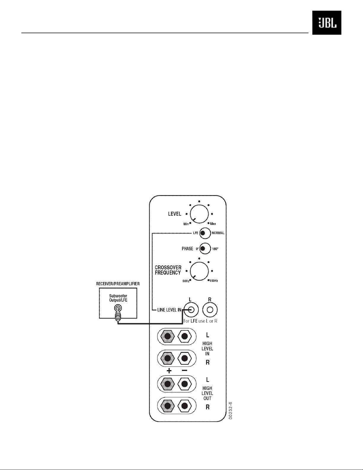
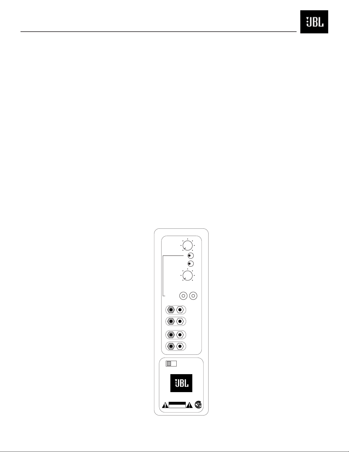
PB12 Subwoofer Controls and Their Function
1. Power - These lights will be red when the unit is
plugged in and not receiving a signal; when the PB12
receives a signal, the lights will cycle to GREEN. If no
signal is received after 10-15 minutes the lights will
cycle back to RED (standby) until a signal is present
again.
2. Level Control - The subwoofer Level Control, PB12,
(located on the rear panel) adjusts the volume of the
subwoofer relative to the rest of the system.
3. LFE/Normal Switch - Ordinarily placed in the Normal
position - but switch to LFE when playing Dolby
®
Digital, DTS®or other digital surround modes - see
page 9.
4. Phase Switch - Changes the subwoofer’s output to
be in phase or 180 degrees out of phase with the
program material.
5. Crossover Frequency - Sets the highest frequency
the subwoofer will reproduce.
6. Line Input - Main Input connection to subwoofer
(preferred).
7. Speaker In Jacks - Main Input connection to
subwoofer when line level, subwoofer, or pre-amp
output connectors are not available, or when a high
pass filter (set at 150Hz) to main loudspeakers is
desired through the Speaker Output Jacks.
8. Speaker Out Jacks - Connected to main
loudspeakers when the Speaker Input Jacks are used.
9. Power Switch - Tu rns the PB12 on or off.
Rear Panel
Front Panel
R
Page 7
PB12
7
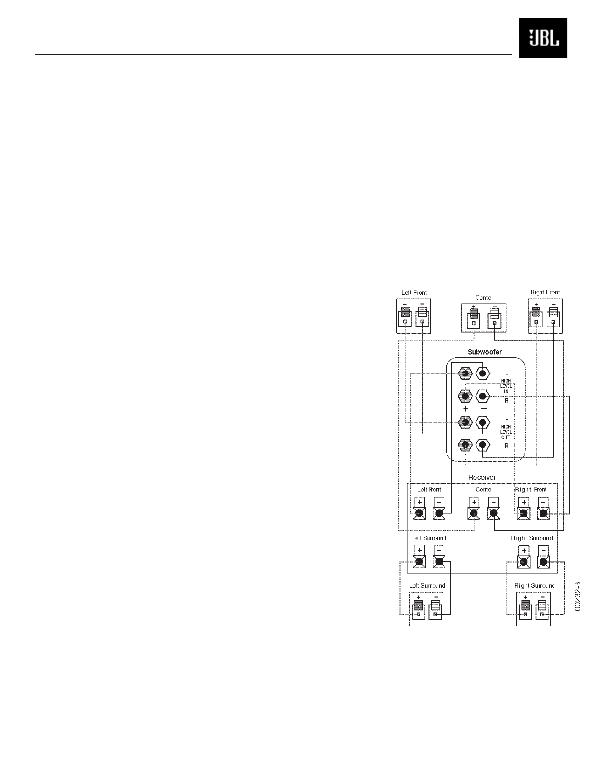
Speaker Connection
When we designed the PB12
powered subwoofers, our goal
was to offer the user the best
possible performance
combined with the most
flexible and complete
installation options. Please
look over the following three
examples to determine which
description best matches
your system and follow the
corresponding hookup
instructions.
To use the binding-post
speaker terminals with bare
wire, unscrew the collar until
the hole through the center-
post is visible under the collar.
Insert the bare end of the wire
through the hole in the post,
then screw the collar back
down until the connection is
tight. The holes in the center
of the collars are intended for
banana-type connectors.
Dolby Pro Logic (Non-Digital) – Speaker Level
Use this installation method for
Dolby Pro Logic applications
(not Dolby Digital, DTS or other
digital processing), where the
receiver/processor does not
have a subwoofer output or a
volume-controlled preamp
(line-) level output:
Connect your receiver or
amplifier’s front left and right
speaker terminals to the left
and right terminals on the
subwoofer that are marked
“High Level In.” Connect the
left and right terminals on the
subwoofer that are marked
“High Level Out” to the
corresponding terminals on
the back of your front left
and right speakers.
Connect your receiver or
amplifier’s center, left and right
surround-speaker terminals to
the corresponding terminals on
the back of your center, left
and right surround speakers.
Page 8

PB12
8
Dolby Pro Logic (Non-Digital) – Line Level
Use this installation method for
Dolby Pro Logic applications
(not Dolby Digital, DTS or other
digital processing), where the
receiver/processor is equipped
with a subwoofer output or a
volume-controlled preamp
(line-) level output:
Use RCA-type patch cords
to connect the line-level
subwoofer outputs on your
receiver or amplifier to the linelevel inputs on the subwoofer.
IMPORTANT: Make sure that
the LFE toggle switch on the
subwoofer is in the “Normal”
position. Do not use the “LFE”
position with Dolby Pro Logiconly processors.
Note: If your receiver or
amplifier only has one
subwoofer output jack,
then you may connect the
subwoofer output on your
receiver/preamplifier to either
the left or right line-level input
on the subwoofer. It makes no
difference which jack you
choose.
Connect each speaker to
the corresponding speaker
terminals on your receiver or
amplifier.
Make sure your receiver or
processor is configured
cor
rectly: Make sure that the
sub
woofer is configured as
“On.”
Note for advanced users: If
your receiver/processor has
a built-in low-pass crossover
filter for the subwoofer output,
then the LFE switch should be
set to the “LFE” position to
bypass the subwoofer’s
internal crossover.
Page 9
PB12
9
Dolby Digital or DTS (or Other Digital Surround Mode) Connection
Use this installation method for
Dolby Digital, DTS or other
digital surround processors:
IMPORTANT: Make sure that
the LFE toggle switch on the
subwoofer is in the “LFE”
position. Use the line-level
input jacks for the LowFrequency Effects channel.
Connect these jacks to the LFE
output or subwoofer output on
your receiver or amplifier.
Note: If your receiver or
amplifier only has one
subwoofer output jack,
then you may connect the
subwoofer output on your
receiver/preamplifier to either
the left or right line-level input
on the subwoofer. It makes no
difference which jack you
choose.
Connect each speaker to
the corresponding speaker
terminals on your receiver
or amplifier.
Make sure that you have
configured your surroundsound processor for
“Subwoofer On” or “LFE On.”
The front left, front right, center
and rear speakers should be
set to “Small” or “Large”
depending on their size and
frequency response. Consult
your receiver’s or processor’s
owner’s manual.
Page 10
PB12
10
OPERATION
Power
When the unit is plugged in
and the power switch is on and
no signal is received, the LEDs
on the front of the unit will turn
red. When a signal is present,
the LEDs will turn green.
Note: It will take several
minutes for the LEDs to turn
from green to red after the
input signal to the subwoofer is
removed. Due to JBL’s unique,
high-output,
high-efficiency
amplifier design, power
consumption is minimal when
the subwoofer is not receiving
a signal.
The subwoofer Level Control
adjusts the volume of the
subwoofer relative to the rest
of the system. Proper level
adjustments depend on several
variables such as room size,
subwoofer placement, type of
main speakers and listener
position. Adjust the subwoofer
level so that the volume of the
bass information is pleasing
to you.
Level Control
Crossover Adjustments
The Crossover Frequency
Control determines the highest
frequency at
which the
subwoofer reproduces
sounds.
If your main speakers can
comfortably reproduce some
low-frequency sounds, set this
control to a lower frequency
setting, between 50Hz – 100Hz.
This will concentrate the
subwoofer’s efforts on the
ultradeep bass sounds required
by today’s films and music. If
you are using smaller bookshelf
speakers that do not extend to
the lower bass frequencies, set
the low-pass crossover control
to a higher setting, between
120Hz – 150Hz. This control is
not used when the LFE switch
is in the “LFE” position.
LEVEL
CROSSOVER
FREQUENCY
PowerBass PB12
LINE LEVEL IN
+ –
ON OFF
POWER
PowerBass PB12
CAUTION
RISK OF ELECTRIC SHOCK
DO NOT OPEN
Min
LFE NORMAL
0º 180º
PHASE
50Hz
L R
For LFE use L or R
HIGH
LEVEL
HIGH
LEVEL
OUT
IN
R
L
R
L
150Hz
120V
60Hz
Max
Page 11

PB12
11
Phase Control
The Phase Control determines
whether the subwoofer’s
piston-like action moves in and
out in phase with the main
speakers or opposite the main
speakers. There is no correct
or incorrect setting. Proper
phase adjustment depends on
several variables such as
subwoofer placement and
listener position. Adjust the
phase switch to maximize bass
output at the listening position.
Remember, every system,
room and listener is different.
There are no right or wrong
settings; this switch offers the
added flexibility to adjust your
subwoofer for optimum
performance for your specific
listening conditions without
having to move your speakers.
If at some time in the future
you happen to rearrange your
listening room and move
your speakers, you should
experiment with the phase
switch in both positions, and
leave it in the position that
maximizes bass performance.
TROUBLESHOOTING
If you used the high-level
(speaker) inputs and there
is no sound from any of the
speakers:
•
Check that receiver/amplifier
is on and a source is playing.
• Check that powered
subwoofer is plugged into
an active electrical outlet
and is switched on.
• Check all wires and
connections between
receiver/amplifier and
speakers. Make sure all wires
are connected. Make sure
none of the speaker wires are
frayed, cut or punctured.
• Review proper operation
of your receiver/amplifier.
If there is low (or no) bass
output:
• Make sure the connections to
the left and right “Speaker
Inputs” have the correct
polarity (+ and –).
• Make sure that the
subwoofer is plugged into an
active electrical outlet and
switched on.
• Adjust the crossover point.
• Flip the Phase Control switch
to the opposite position.
• If you are using a Dolby
Digital/DTS receiver or
processor, make sure that the
subwoofer adjustments on
the receiver/processor are
set up correctly.
• Slowly turn the Level
Control clockwise until you
begin to hear the desired
amount of bass.
If you used the line-level
inputs and there is no sound
from the subwoofer:
•
Check that receiver/amplifier
is on and a source is playing.
• Check that powered
subwoofer is plugged into an
active electrical outlet and is
switched on.
• Check all wires and
connections between
receiver/ amplifier and
subwoofer. Make sure all
wires are connected. Make
sure none of the wires are
frayed, cut or punctured.
• Review proper operation of
your receiver/amplifier.
• Slowly turn the Level
Control clockwise until you
begin to hear the desired
amount of bass.
• Make sure that you have
configured your receiver/
processor so that the
subwoofer/LFE output is on.
Page 12
PB12
12
PB12 TEST SETUP AND PROCEDURE
General Function
UUT = Unit Under Test
1. Connect one line level input cable (RCA) from signal generator to either Right or Left Level input on UUT. VOLUME
control should be full conterclockwise. Make sure the LFE/Normal switch is in the NORMAL position.
2. Turn on generator, adjust to 100mV, 50Hz.
3. Plug in UUT; Turn Main Power switch ON. LED’s on the front panel may be either Red or Green. Turn VOLUME
control full clockwise. Low Pass control should be set fully clockwise (150Hz).
4. LED should turn Green; immediately bass response should be heard and felt from port tube opening.
5. Turn off generator, turn VOLUME control fully counterclockwise, disconnect RCA cables.
6. Connect one pair of speaker cables to either high level input terminal on UUT. Cables should be connected to an
integrated amplifier fed by the signal generator.
7. Turn on generator and adjust so that speaker level output is 1.0V, 50Hz. Tu rn VOLUME control full clockwise.
8. Green LED should light, immediate bass response should be heard and felt from the port tube opening.
Sweep Function
1. Follow steps 1-4 above, using a sweep generator as a signal source.
2. Sweep generator from 20Hz to 300Hz. Listen to the cabinet and drivers for any rattles, clicks, buzzes or any other
noises. If any unusual noises are heard, remove driver and test.
Driver Function
1. Remove driver from cabinet; detach + and – wire clips.
2. Check DC resistance of driver; it should be 4.8 ohms.
3. Connect a pair of speaker cables to driver terminals. Cables should be connected to an integrated amplifier fed by a
signal generator and adjust so that speaker level output is 5.0V.
4. Sweep generator from 20Hz to 1kHz. Listen to driver for any rubbing, buzzing, or other unusual noises.
CD PLAYER
PRE AMP
AMPLIFIER
AC VOLT
SPEAKER
LEVEL
METER (6V)
LINE LEVEL
UNDER TEST
FROM
LINE-LEVEL
SOURCE
PB12
SPEAKER
OUTPUT
FROM
AMPLIFIER
LEVEL
Min Max
PHASE
CROSSOVER
FREQUENCY
50 Hz 150 Hz
PowerBass PB12
LR
LINE LEVEL IN
FOR LFE USE L or R
LFE
NORMAL
180
0
L
HIGH
LIVEL
IN
R
L
HIGH
LIVEL
OUT
R
00229
Page 13
PB12
13
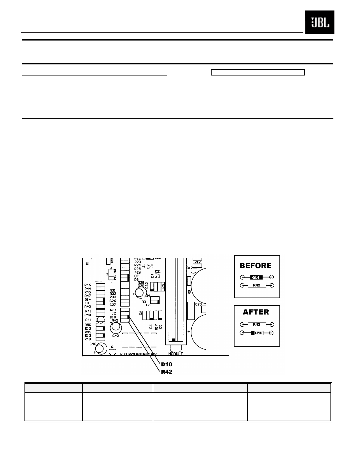
Service Bulletin
Service Bulletin JBL2001-03 Rev1 – January 2002 This is considered a Minor repair
To: All JBL Service Centers
Models: PB10, PB12 (Revision 1 only)*
Subject: Unit Will Not Switch to Standby Mode
When the power cord of the PB series subwoofer is plugged into a wall outlet (and for the PB12 only, the power
switch is on), and an audio signal is present, the LED’s on the cabinet face will turn green, indicating the
subwoofer is in the ON mode. With the audio signal removed, it will take 10 - 15 minutes for the LEDs to turn
from green to red, indicating the subwoofer is now in the STANDBY mode. Power consumption is minimal in this
mode.
In the event you receive a PB10 or PB12 subwoofer with the complaint: “The unit will not switch to
standby mode, even when the audio signal is removed” (indicated by the subwoofer’s green LED’s
remaining on), perform the following modification:
1) Set the unit on a padded surface and remove all external cables.
2) On the amplifier faceplate, remove the (10) Phillips mounting screws around the perimeter.
3) Remove the amplifier assembly from the enclosure. If the amp is turned and supported correctly, no other
connectors need to be unplugged.
4) Locate Zener Diode D10 and Resistor R42 (22kΩ). See illustration. These parts must be “swapped”, i.e.,
R42 soldered into the D10 location, and D10 soldered into the R42 location. VERY IMPORTANT: Observe
polarity on D10 in new location.
5) Replace amplifier; test subwoofer to assure the unit goes into the standby mode 10 - 15 minutes after
removing the Audio input signal.
Mode l S e r i al num be r S ta tus Ac ti on
PB10 *
PB12 *
Al l ser i al number s
af f ect ed
Unit may not switch to Standby mode
Swap locations:
Zener Diode D10,
Resistor R42 (22kΩ).
Observe D10 polarity.
* Revision 1 of the PB10/12: Amplifier faceplate says “Made in Canada”; Amplifier serial number starts with “AM”
Black (or silver) potted, non-serviceable S53/64AMI output module. PB10 only – No Power switch
Page 14
PB12
14
Service Bulletin
Service Bulletin JBL2001-04 Rev1 – January 2002 This is considered a Minor repair
To: All JBL Service Centers
Models: PB10, PB12 (Revision 1 only)*
Subject: Hum, Buzz or “Thumping”
In the event you receive a PB10 or PB12 subwoofer complaint: “There is an audible hum or buzz”, or the subwoofer
“thumps” or “pops” every 10 seconds, then review the conditions below to determine the most effective solution:
A) Audible Hum with unit on, Green LED is ON, hum disappears completely when the connecting input cables (RCA or
Speaker-Level) are disconnected:
Very long runs of line-level input cables, particularly in parallel with AC power cords, may induce hum in the audio
cables. Check audio cables for defects, broken ground connections, or replace low quality cables. Try plugging the
AC power cord from the subwoofer into a different AC service outlet other than the outlet the rest of the audio
equipment is plugged into.
B) Mild Audible Hum under all circumstances when power cord is plugged in outlet. Hum level does not change whether the
LED’s are Red or Green, or input cables are connected or disconnected. Level control adjustments do not change the
hum level.
This is a mechanical hum caused by the power transformer. Note that a slight hum, within design limits, may be
noticeable in a very quiet room, when you are close to the unit. This is acceptable within the PB10’s product and
price category to most customers, but not to others. If the mechanical hum is unacceptable to the customer, then
replace Power Transformer. PB10: JBL part# 80135. PB12: JBL part# 80116
C) Loud Hum, under all circumstances. It may be louder when LED’s are Green vs. Red ; it may be affected by the position
of the Level control. The subwoofer may “thump” or “pop” approximately every 10 seconds.
Reset the digital subwoofer amplifier by unplugging the AC power cord. Wait 30 seconds, then plug the cord back in.
Repeat this 2-3 times if necessary.
For #C only - If the unit still does not function correctly, then replace Power Amp Module S53/64AMI as per
instructions below: PB10: JBL part# 60301 PB12: JBL part# 60302
1) Set the unit on a padded surface and remove all external cables.
2) On the amplifier faceplate, remove the (10) Phillips mounting screws around the perimeter.
3) Remove the amplifier assembly from the enclosure. If the amp is supported correctly, no other connectors need to be
unplugged.
4) Locate the Power Amp Module S53/64AMI, see location on the following page. It is the large black or gray component
with a metal case. On the solder side of the circuit board are 28 soldered connections. NOTE: See special handling
instructions for S53/64AMI on the following page.
5) Replace the amplifier assembly back into the cabinet; replace the screws.
6) Test the unit and confirm the original problem has been corrected. NOTE: THE PB10/12 REVISION 1 AMPLIFIER
MUST ALWAYS BE TESTED WITH A WOOFER OR 4 OHM RESISTIVE LOAD.
MODEL Ser i al Number (120v)
Serial numbers are located on the cabinet directly
PB10 See ser i al number s on Page 3 for fac t o r y
PB12 Hum, Buzz or “Thumping” Repl ac e Power Amp Modul e S64AMI
* Revision 1 of the PB10/12: Amplifier faceplate says “Made in Canada”; Amplifier serial number starts with “AM”
below the amplifier faceplate.
Hum, Buzz or “Thumping” Repl ac e Power Amp Modul e S53AMI
modi fi ed uni t s
STATUS ACTI ON
for symptoms described in #C only
for symptoms described in #C only
Black (or silver) potted, non-serviceable S53/64AMI output module. PB10 only – No Power switch
Page 15
PB12
15
+6V 15
16
17
V+
1 +6V
2
V+3
18
4
O/P
19 5
O/P
20
6
V- V-
21 7
22
8
SD 24
+15V 23 9 +15V
10 SD
FR 25 11 FR
I/P 26 12 I/P
GND 27 13 GND
-15V 28 14 -15V
00228
NOTE: THE FOLLOWING PROCEDURES MUST BE
FOLLOWED WHEN INSTALLING NEW S53AMI/S64AMI
AMP MODULES:
FAILURE TO FOLLOW ONE OR MORE OF THESE STEPS
MAY RESULT IN THE INSTANT DESTRUCTION OF THE
MODULE WHEN POWERED UP.
1. Align white indent marker on Amp Module with indent
marker on main PCB; alternately observe position of label
on top of the Module; incorrectly replacing the Module
180° in the PCB slot will result in its destruction.
2. All AC powered test instruments (meters, oscilloscopes,
etc.) must have a floating ground, i.e., be connected to
an isolation transformer.
3. Align and position the Amp Module before soldering.
4. Attach the Amp Module with the mounting screws before
soldering or powering up.
5. Use only rosin-core or non-acid core solder; thoroughly
de-flux the surfaces after soldering.
If the new S53AMI/S64AMI Amp Module has larger mounting
hole(s) in the case, and the stock screws no longer will fit,
and screws of the proper type cannot be obtained locally
order:
(2) part# 60301S (screws)
(2) part# 60301N (nuts)
S53AMI/S64AMI - Power Amp Module SAFETY PART
PB10/12 Revision 1 Only
Page 16
PB12
16
Service Bulletin
Service Bulletin JBL2001-05 Rev2 - February 2002 This is considered a Minor repair
To: All JBL Service Centers
Models: PB12 (Revision 1 only)*
Subject: Popping Every Few Seconds During Play
In the event you receive a PB12 subwoofer with the complaint: “The subwoofer “thumps” or “pops”
every few seconds of play”, follow the procedure below:
Probable Cause:
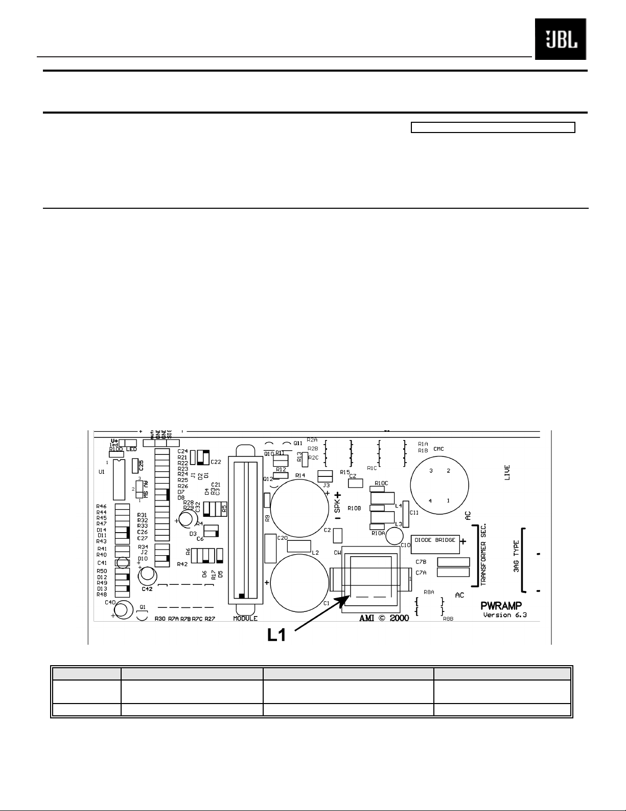
Inductor L1 (220uH) may be damaged.
Check and Replace L1 if necessary:
1) Set the unit on a padded surface and remove all external cables.
2) On the amplifier faceplate, remove the (10) Phillips mounting screws around the perimeter.
3) Remove the amplifier assembly from the enclosure. If the amp is supported correctly, no other
connectors need to be unplugged.
4) Locate Inductor L1 on the main PCB. If the windings appear charred or burnt, it must be replaced.
5) Order JBL part# 80121 and replace L1.
6) Replace the amplifier assembly back into the cabinet; replace the screws.
7) Test the unit and confirm the original problem has been corrected.
Model Serial number (120V) Status Action
PB12 * AM0035-24318 and below L1 may be damaged
if experiencing above symptoms
PB12 * AM0035-24319 and above Modified by factory None required
* Revision 1 of the PB12: Amplifier faceplate says “Made in Canada”; Amplifier serial number starts with “AM”
Black (or silver) potted, non-serviceable S64AMI output module.
Replace L1
with JBL part# 80121
Page 17
PB12
17
Service Bulletin
Service Bulletin JBL2001-07 Rev1 - February 2002 This is considered a Minor repair
To: All JBL Service Centers
Model: PB12 (Revision 1 only)*
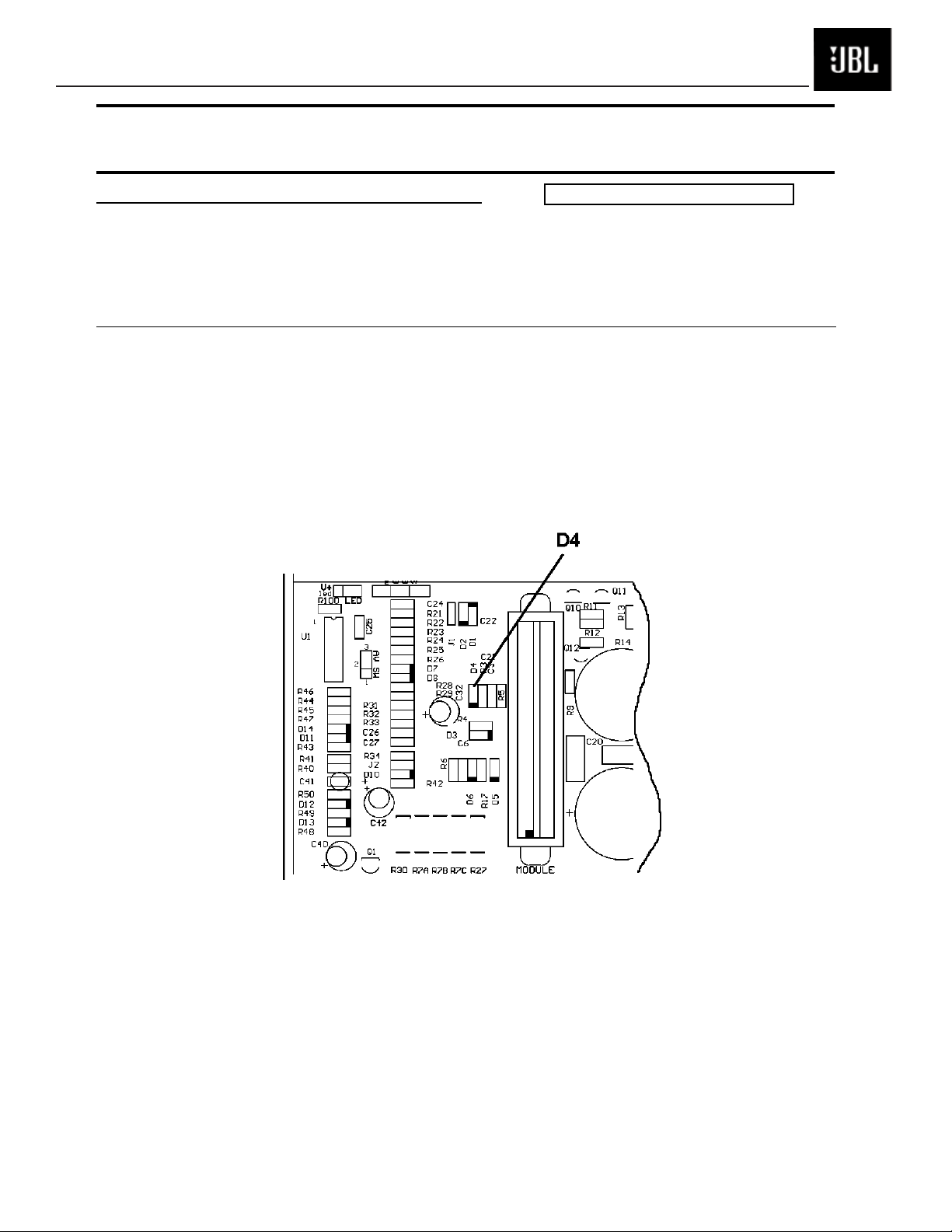
Subject: Possible Missing Diode D4
In the event you receive a PB12 subwoofer for any servicing reason, check for the presence of
diode D4 on the Main PCB close to the Power Amp Module (see illustration). If D4 is missing or
has been “cut out” of the circuit, it should be replaced; add JBL part# 50115. Observe polarity.
Note: The presence or absence of D4, in itself, does not contribute to, or solve, an amplifer failure.
Purpose of D4 is to reduce the possibility of an occasional Turn-OFF pop noise.
Reference for general location only; all parts or designators may not conform exactly to this drawing.
* Revision 1 of the PB12:
Amplifier faceplate says “Made in Canada”; Amplifier serial number starts with “AM”
Black (or silver) potted, non-serviceable S64AMI output module.
Page 18

PB12
18
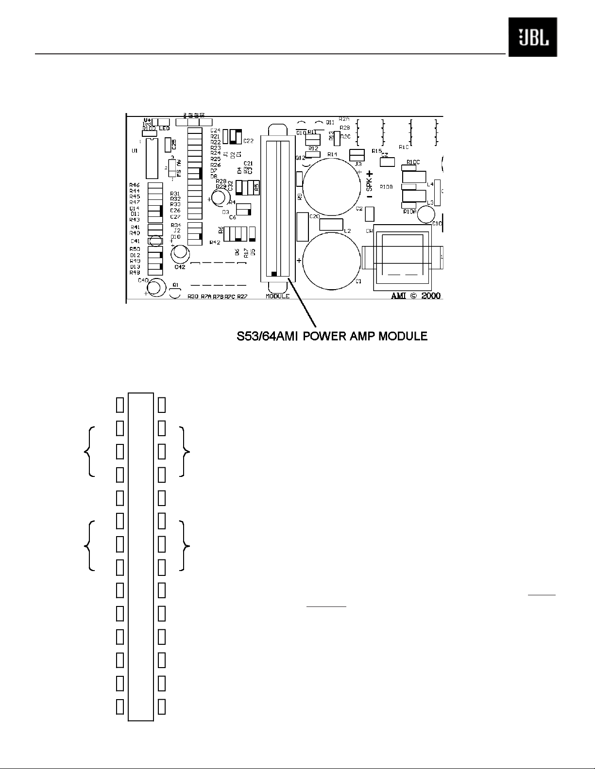
Exploded and Packaging Views
(IMAGE REDUCED)
1
5
9
4
2
6
7
8
3
Identification Of PB12 Revisions 1 and 2 can be found on Page 2.
MECHANICAL & PACKING PARTS LIST
Item # Description Qty Revision 1 Part# Revision 2 Part#
1 12" Woofer 1 203400 338128-001
2 Foot 4 203410 336486-001
3 Outer Carton 1 203420 338131-001
4 Owner’s Manual 120V 1 203430 338129-001
Survey Card 1 331384-001
Warranty Card 1 331994-001
5 Amplifier Complete 1 Not For Sale Not For Sale
6 Foot Screw 4 203411 763-31110-40
7 Foam corners (Top Corners) 4 203460 338132-001
8 Foam corners (Bottom Corners) 4 203470 338132-001
9 Port tube 1 Not For Sale 336799-001
Page 19

PB12
19
Amplifier Exploded View (Revision 1 Only)
00263
1
2
5
6
3
4
7
LEGEND
1 Dual RCA jack 108320
2 Power Transformer 80116
3 Level Pot 40402
4Crossover CONTROL 40707
5 Fuse Clips (2) 70323
6 2A SLO-BLO T TypeFuse (3AG) 80117
7 Power Switch 70151
Page 20

PB12
20
Amplifier Faceplate/Access
CROSSOVER
FREQUENCY
LEVEL
LINE LEVEL IN
PHASE
Min
Max
L
R
L R
For LFE use L or R
LFE NORMAL
PowerBass PB12
REMOVE THESE TWO SCREWS
TO REMOVE REAR COVER
AND ACCESS AMPLIFIER
LONGER SCREW HERE
PowerBass PB12
HIGH
LEVEL
IN
L
R
POWER
HIGH
LEVEL
OUT
+ –
120V
60Hz
50Hz
0º 180º
150Hz
CAUTION
RISK OF ELECTRIC SHOCK
DO NOT OPEN
ON OFF
1
2
10
5
6
4
7
8
9
3
MECHANICAL & PACKING PARTS LIST
Item # Description Qty Revision 1 Part# Revision 2 Part#
1 Level Knob 1 70313 061-020000-000
2 LFE Defeat Switch 1 70150 074-030002-000
3 PB12 faceplate 1 70325 n/a
4 HI LEVEL Input/Output Jacks 4 108116 072-060170-000
5 Phase Switch 1 70150 074-030002-000
6Crossover Frequency Knob 1 70313 061-020000-000
7 Strain Relief Plug 1 70305 061-314002-000
8 Power Cord 1 80105 083-041802-009
9 Power Switch 1 70151 074-020018-000
10 RCA Input jacks 1 108324 072-010007-000
Identification Of PB12 Revisions 1 and 2 can be found on Page 2.
Page 21

PB12
21
Integrated Circuit Diagrams (Revision 1 Only)
+6V 15
16
17
V+
1 +6V
2
V+3
18
4
O/P
19 5
O/P
20
6
V- V-
21 7
22
8
SD 24
+15V 23 9 +15V
10 SD
FR 25 11 FR
I/P 26 12 I/P
GND 27 13 GND
-15V 28 14 -15V
00228
NOTE: THE FOLLOWING PROCEDURES MUST BE
FOLLOWED WHEN INSTALLING NEW S53AMI/S64AMI AMP
MODULES:
FAILURE TO FOLLOW ONE OR MORE OF THESE STEPS
MAY RESULT IN THE INSTANT DESTRUCTION OF THE
MODULE WHEN POWERED UP.
1. Align white indent marker on Amp Module with indent
marker on main PCB; alternately observe position of label
on top of the Module; incorrectly replacing the Module
180° in the PCB slot will result in its destruction.
2. All AC powered test instruments (meters, oscilloscopes,
etc.) must have a floating ground, i.e., be connected to
an isolation transformer.
3. Align and position the Amp Module before soldering.
4. Attach the Amp Module with the mounting screws before
soldering or powering up.
5. Use only rosin-core or non-acid core solder; thoroughly
de-flux the surfaces after soldering.
If the new S53AMI/S64AMI Amp Module has larger mounting
hole(s) in the case, and the stock screws no longer will fit,
and screws of the proper type cannot be obtained locally
order:
(2) part# 60301S (screws)
(2) part# 60301N (nuts)
S53AMI/S64AMI - Power Amp Module SAFETY PART
NOTE: THE PB10/12 REVISION 1 AMPLIFIER MUST ALWAYS BE TESTED
WITH A WOOFER OR 4 OHM RESISTIVE LOAD.
N-Chan JFET
LM324, TLO64, U1, U2
Q1 2N5457
D
S
G
MPSA56, Q10, Q11
2
Base
1
2
3
3 Collector
1 Emitter
2N4401, Q12
2
Base
1
2
3
3 Collector
1 Emitter
0227
Page 22

PB12
22
Integrated Circuit Diagrams (Revision 2 Only)
2N5401
Q1
3 Collector
2
Base
1
2
3
1 Emitter
MPSW06RLRA,
MPSW56RLRAMPQ,
MPS2222ARLRA,
2N2907A, 2N5551,
Q2, 16, 3, 21, 19, 23, 17
3 Collector
2
Base
1
2
3
1 Emitter
OPAMP, QUAD
TL074CDR
U2, 3
BEVE L
OPAMP, DUAL
TL072CDR SO-8,
NJM4558M-TE3
U5, 6, 4
MOSFET IRF640
Q18, 22
1. G
2. D
3. S
3
12
TIP31C
Q4
MMBT3904LTI SOT23,
MMBT3906LTI SOT23,
DTC114EK SMT3,
MMBT5401 LTI,
MMBT5551 LTI
Q11, 14, 13, 5, 8, 9, 6, 10,
12, 15, 7, 20, 24, 26, 25
IR2111 HALF-BRIDGE
DRIVER
U7
BC
E
Page 23

PB12
23
PB12 Testing Procedure (Revision 1 Only)
Page 24

PB12
24
PB12 Testing Procedure (Cont.) (Revision 1 Only)
Page 25

PB12
25
PB12 Testing Procedure (Cont.) (Revision 1 Only)
Page 26

PB12
26
PB12 Testing Procedure (Cont.) (Revision 2 Only)
A. Power Amp Section
Resistance
Check
Resistance from S+ (SPK O/P) to GND should be >1M Ω (NO LOAD)
Resistance from V+ (C6 P+) to V- (C8 P-) gradually Fully CHARGED should read >10k Ω
Resistance from V+ (C6 P+) to S+ (SPK O/P) should read >1MΩ
Resistance from V- (C8 P-) to S+ (SPK O/P) should read >1M Ω
2. Power Up LED RED
With a 5mV signal to Low level input, LED should change to GREEN
-Voltage measurements (DVM)
OP AMP
LED
P-U4(1) P-U4(7)
RED 0Vrms 11.84VDC
GREEN 7.13Vrms -12.93VDC
3. D.C. Operation
-Voltage measurements (DVM) on CLASS D POWER AMP
Between V+ Q4(E) Q1(C)
And This
Point
Get this
Reading
GND V- GND GND GND GND GND GND GND GND
71.7V 0V -71.7V 0V -71.7V -71.5V -71.2V 0V 0V 4.65V
Q10(C)
U7(1) U7(2) U7(4) U7(6) U7(7) U7(8)
4. Check Switching Frequency
• Oscilloscope - USE THE PROBE TIP TO U6(7) TO GND
• Reading 100kHz +/-10%,24Vp-p
B. Pre Amp Section
Line Level Input Sensitivity
-Set up Turn level, X’OVER FREQ POT Fully CW and LFE switch off
Generator Set at 200mV@50Hz
Signal to Line level input
Page 27

PB12
27
PB12 Testing Procedure (Cont.) (Revision 2 Only)
- Voltage measurements
OP AMP
U2(1) U2(14) U2(8) U3(7) U3(1) U3(14) U3(8) U5(7) U5(1)
306.9mV 461mV 460mV 658mV 628mV 598mV 2.326V 2.02V 3.57V 23.33V
2. High Level Input Sensitivity
-Set up Turn level, X’OVER FREQ POT Fully CW and LFE switch off
Set Generator at 1.3V@50Hz
Signal to High level input
-Voltage measurements 15.3V at speaker output
3. Low-Pass
-Set up Set Generator at 200 mV@100Hz
Signal to
Measure voltage at S+ speaker output
-Voltage measurement
X’OVER FREQ. Setting Output
CW 14.03V
CCW 4.8V
Line level input
SPEAKER
O/P
4. LFE
-Set up Set Generator at 200mV@200Hz
Signal to
Measure voltage at S+ speaker output
LFE switch Setting Output
Normal 6V
LFE 18.32V
See flow chart next page for diagnostics.
Line level input
Page 28

PB12
28
PB12 Testing Procedure (Cont.) (Revision 2 Only)
,
PB12 POWER MODULE TESTING FLOW CHART
TO GROUND. ALL TEST INSTRUMENTS CONNECTED TO THE OUTPUT MUST
BE FLOATING. ATTACH THE SCOPE PROBE TIP TO S - and REFERENCE
LEAD TO S+.
(A 10mV signal may need from the input to trigger the Switch turn on)
START
Resistance check
(no load)
between V+ V-,
V+ O/P,V- O/P
and O/P to GND
is > 10K
no
no
OK
yes
yes
Power up with no
signal input
LED RED
no
no
OK
yes
yes
Check Q4(E)
TO V-
= 0V D.C.
CAUTION : SPEAKER OUTPUT IS FLOATING AND IS NOT PROTECTED AGAINST A SHORT
Check +/-15V-MOD
+/-15V voltage at
U 6(8),U6(4)
Replace
Q18,Q22
Discharge C37,
Check fuse
transformer, L4,
rectifier, C6 and C8
OK
I/P:10mv/50HZ
Check +15V/SW
Q4(E) TO V-
OK
Check
U7(1) = -58.3V
Check
FB1,FB2,C45,
C50,C60,C63,
R81,R82
Check
MUTE(-12.9V),
And
Q24,Q25,Q26
no
no
OK
yes
yes
Use scope to check
switching
frequency U6(7)
100KHz
+/-10% , ~24Vp-p
no
no
OK
yes
yes
CLASS D AMP OK
Check
MUTE(+8V) and
Q24,Q25,Q26
OK
Use scope to
check O/P U7(6)
and GND
143Vp-p square
wave shown
OK
Check
L2,L3,C71,C72,
C73
C74
Check
U7,Q16,Q17,
Q20,Q21,R87,
D26,D35,C64
Page 29

29
PB12 Block Diagram Revision 2 Only
1
2
3
4
A
SPEAKER LEVEL
INPUT
PHASE CTRL
SWITCH
5
RevNo Revision note
6
7
Date Signature
8
Checked
A
Rin
Lin
B
Rout
DIF. AMP
SUMMI NG AMP
VOLUME CTRL
AMP STAGE
HPF
12dB/Octave
LPF
12dB/Octave
LPF
Variable
12dB/Octave
B
Lout
Line Level
Input
C
D
SIGNAL SENSE
SIGNAL SENEING
MUTE
ATO
* FUSE
DC OFFSET
PROTECTION
THERMAL
PROTECTION
CURRENT
PROTECTION
LINEAR
POWER SUPPLY
MUTE
CLASS D
AMPLIFIER
LIMITER /
LPF
OUTPUT-RELAY
SUMMI NG AMP
LFE
NORMAL
C
D
5.6 OHMS
EXTERNAL LED INDICATORS
E
CONTROLLED
REGULATOR
+15V SW
E
MUTE
NOTE :
120 VAC T2A-250V
F
230 VAC T1.25A-250V
1
2
3
6
7
8
F
Page 30

PB12
30
PB12 Electrical Parts List (Revision 1 Only)
PB12 POWER AMP section of PCB Version 6.3 -7.0.
Part # Designator Description
50100 BR RECT RS604 6AMP Bridge rectifier
50105 D1 1N4744A 15V 1w Zener
50112 D10 1N5242B 12V .5w Zener
50104 D11 1N4148 Sig Diode
50112 D12 1N5242B 12V .5w Zener
50104 D13 1N4148 Sig Diode
50104 D14 1N4148 Sig Diode
50105 D2 1N4744A 15V 1w Zener
50114 D3 1N5265B 62V .5w Zener
50104 D4 1N4148 Sig Diode
50113 D5 1N4735A 6.2V 1W
50103 D6 1N5234B 6V .5w Zener
50104 D7 1N4148 Sig Diode
50104 D8 1N4148 Sig Diode
60157 Q1 2N5457 25V N-chnl FET
60155 Q10 2N5401 120V PNP 600mA
60155 Q11 2N5401 120V PNP 600mA
60156 Q12 2N4401 40V NPN 600mA
60102 U1 TLO64 Quad OpAmp
Capacitors
30710 C1 2200uF 100V +80 / -20 Electrolytic 105C
30718 C10 4u7F 100V BP/NP Electr DF<.1
30523 C11 330nF 100V mono ceramic
30710 C2 2200uF 100V +80 / -20 Electrolytic 105C
30532 C20 220nF 250V metallized polyester
30502 C21 100nF 50V mono ceramic
30502 C22 100nF 50V mono ceramic
30527 C24 330nF 50V mono ceramic
C25 NOT USED
30508 C26 10nF 50V mono ceramic
30513 C27 3n3F 50V mono ceramic
30502 C3 100nF 50V mono ceramic
30711 C32 22uF 35V +80/-20 Electrolytic
30715 C40 10uF 16V +80/-20 Electrolytic
30716 C41 1uF 16V +80/-20 Electrolytic
30717 C42 100uF 16V +80/-20 Electrolytic
30502 C6 100nF 50V mono ceramic
30521 C7A 100nF 250V ceramic/film
30521 C7B 100nF 250V ceramic/film
CW NOT USED
30505 CZ 100nF 100V ceramic/film
Page 31

PB12
31
PB12 Electrical Parts List (Revision 1 Only)
PB12 POWER AMP section of PCB Version 6.3 -7.0.
Part # Designator Description
Resistors
R100 NOT USED
40105 R10A 0.1R .5W metal
40105 R10B 0.1R .5W metal
40105 R10C 0.1R .5W metal
40420 R11 1k .25W carbon
40420 R12 1k .25W carbon
40417 R13 47k .25W carbon
40718 R14 3k3 .25W carbon
R15 NOT USED
40735 R1A 7k5 2W metal
40735 R1B 7k5 2W metal
40735 R1C 7k5 2W metal
40405 R21 4K7 .25W carbon
40736 R22 42K2 .25W metal
40737 R23 187k .25W metal
R24 NOT USED
R25 NOT USED
40722 R26 6k8 .25W carbon
40738 R27 10k 2W metal
40739 R28 1k2 0.25W carbon
40739 R29 1k2 0.25W carbon
40735 R2A 7k5 2W metal
40735 R2B 7k5 2W metal
40735 R2C 7k5 2W metal
40703 R3 8M2 .25W carbon
40738 R30 10k 2W metal
40417 R31 47k .25W carbon
40417 R32 47k .25W carbon
40427 R33 23k7 .25W metal
40403 R34 10k .25W metal
40740 R4 33k 1W metal
40420 R40 1k .25W carbon
40701 R41 1000k .25W carbon
40741 R42 22k .5W metal
40701 R43 1000k .25W carbon
40406 R44 100k .25W carbon
40415 R45 470K .25W carbon
40701 R46 1000k .25W carbon
40409 R47 10k .25W carbon
40409 R48 10k .25W carbon
40726 R49 15k .25W carbon
40732 R5 56k2 .25W metal
40727 R50 2k2 .25W carbon
40111 R6 47R .25W carbon
40738 R7A 10k 2W metal
40738 R7B 10k 2W metal
40738 R7C 10k 2W metal
40738 R8A 10k 2W metal
40738 R8B 10k 2W metal
R9 NOT USED
Page 32

PB12
32
PB12 Electrical Parts List (Revision 1 Only)
PB12 POWER AMP section of PCB Version 6.3 -7.0.
Part # Designator Description
Miscellaneous
80121 L1 220uH 5 Amp Gapped Ecore choke
80122 L2 8u5H 5 Amp ferrite bead
80122 L3 8u5H 5 Amp ferrite bead
80122 L4 8u5H 5 Amp ferrite bead
80100 CMC 2m2H 5 Amp choke
60302 MODULE S64AMI
108326 Led Harness With two LED's,Molex plug Glued into cabinet
80116 Transformer MCI4632 100VA 4632 transformer
70151 Switch SW SPST Power Switch
70322 LED socket PCB mount LED socket
80117 3AG FUSE 2A SloBlo T type
70324 0.187" PCB Tabs 7
70323 PCB Fuse Holders 2
70325 PB12 faceplate PB12 faceplate
80105 Power cord Power cord
70305 Strain relief Strain relief
PB12 PREAMP PCB Version #6.3
Part # Designator Description
Semiconductors
60102 U1 TLO 64 OP amp
60100 U2 LM324 OP amp
Capacitors Film Caps may be used in any position EXCEPT C1,C2
30707 C1 200uF 50V BP Electrolytic
30504 C10 100nF 50V mono ceramic
30504 C11 100nF 50V mono ceramic
30504 C12 100nF 50V mono ceramic
30504 C13 100nF 50V mono ceramic
30530 C16 100nF 50V mono ceramic
30531 C17 150nF 50V mono ceramic
30100 C18 330pF 50V mono ceramic
30100 C19 330pF 50V mono ceramic
30707 C2 200uF 50V BP Electrolytic
30502 C20 100nF 50V mono ceramic
30502 C21 100nF 50V mono ceramic
30502 C22 100nF 50V mono ceramic
30502 C23 100nF 50V mono ceramic
30101 C3 220pF 50V mono ceramic
C30 NOT USED
30101 C4 220pF 50V mono ceramic
30101 C5 220pF 50V mono ceramic
30101 C6 220p 50V mono ceramic
C7 0r
C8 0r
40730 C9 1k .25W Metal Resistor
Page 33

PB12
33
PB12 Electrical Parts List (Revision 1 Only)
PB12 POWER AMP section of PCB Version 6.3 -7.0.
Part # Designator Description
Resistors
40405 R1 4k7 .25W carbon
40409 R10 10k .25W carbon
40731 R11 59k .25W carbon
40504 R12 45k3 .25W metal
40412 R13 33k2 .25W metal
40709 R14 68k1 .25W metal
R15 NOT USED
R16 NOT USED
40732 R17 56k2 .25W metal
40722 R18 6k8 .25W carbon
40722 R19 6k8 .25W carbon
40405 R2 4k7 .25W carbon
40722 R20 6k8 .25W carbon
R21 0r
40722 R22 6k8 .25W carbon
R23 0r
40109 R24 604r .25W metal
40412 R25 33k2 .25W metal
40405 R26 4k7 .25W metal
40109 R27 604r .25W metal
40412 R28 33k2 .25W metal
40406 R3 100k .25W carbon
40403 R30 10k .25W metal
40733 R33 12k1 .25W metal
40734 R34 120k .25W metal
40451 R35 137k .25W metal
40406 R4 100k .25W carbon
40406 R5 100k .25W carbon
40406 R6 100k .25W carbon
40717 R8 2k7 .25W carbon
40717 R9 2k7 .25W carbon
Miscellaneous
108320 RCA CONNECTOR DUAL RCA-yellow
108116 HI LEVEL I/O Binding Post OUT Binding Post
108116 HI LEVEL I/O Binding Post IN Binding Post
40402 LEVEL 5k POT Log (A) Pot
40707 Crossover CONTROL 20k POT Lin (B) Pot.
70150 LFE switch SW SPDT mini-Toggle
70150 Phase Switch SW SPDT mini-Toggle
Page 34

PB12
34
PB12 Electrical Parts List (Cont.) (Revision 1 Only)
PB12 POWER AMP section of PCB Version 7.2.
Part # Designator Description
Resistors
40735 R1A 7k5 2W 5% metal SAFETY
40735 R1B 7k5 2W 5% metal SAFETY
40735 R1C 7k5 2W 5% metal SAFETY
40735 R2A 7k5 2W 5% metal SAFETY
40735 R2B 7k5 2W 5% metal SAFETY
40735 R2C 7k5 2W 5% metal SAFETY
40703 R3 8M2 .25W 5% carbon
40740 R4 33k 1W 5% metal SAFETY
40732 R5 56k2 .25W 1% metal
40111 R6 47 ohms .25W 5% carbon
40738 R7A 10k 2W 5% metal SAFETY
40738 R7B 10k 2W 5% metal SAFETY
40738 R7C 10k 2W 5% metal SAFETY
40738 R8A 10k 2W 5% metal SAFETY
40738 R8B 10k 2W 5% metal SAFETY
R9 NOT USED
40105 R10A 0.1 ohms .5W 5% metal
40105 R10B 0.1 ohms .5W 5% metal
40105 R10C 0.1 ohms .5W 5% metal
40420 R11 1k .25W 5% carbon
40420 R12 1k .25W 5% carbon
40417 R13 47k .25W 5% carbon
40718 R14 3k3 .25W 5% carbon
R15 NOT USED
40405 R21 4K7 .25W 5% carbon
40736 R22 42K2 .25W 1% metal
40737 R23 187k .25W 1% metal
R24 NOT USED
R25 NOT USED
40722 R26 6k8 .25W 5% carbon
40738 R27 10k 2W 5% metal SAFETY
40739 R28 1k2 0.25W 5% carbon
40739 R29 1k2 0.25W 5% carbon
40738 R30 10k 2W 5% metal SAFETY
40417 R31 47k .25W 5% carbon
40417 R32 47k .25W 5% carbon
40427 R33 23k7 .25W 1% metal
40403 R34 10k .25W 1% metal
40407 R35 220K .25W 5% carbon
40420 R40 1k .25W 5% carbon
40701 R41 1000k .25W 5% carbon
40741 R42 22k .5W 5% metal
40701 R43 1000k .25W 5% carbon
40406 R44 100k .25W 5% carbon
40415 R45 470K .25W 5% carbon
40701 R46 1000k .25W 5% carbon
40409 R47 10k .25W 5% carbon
40409 R48 10k .25W 5% carbon
40726 R49 15k .25W 5% carbon
40727 R50 2k2 .25W 5% carbon
Page 35

PB12
35
PB12 Electrical Parts List (Cont.)
PB12 POWER AMP section of PCB Version 7.2.
Part # Designator Description
Capacitors
30710 C1 2200uF 100V +80/-20 Electrolytic 105C SAFETY
30710 C2 2200uF 100V +80/-20 Electrolytic 105C SAFETY
30502 C3 100nF 50V 20% mono ceramic
30502 6 100nF 50V 20% mono ceramic
30521 C7A 100nF 250V 20% ceramic/film SAFETY
30521 C7B 100nF 250V 20% ceramic/film SAFETY
30718 C10 4u7F 100V 20% BP/NP Electr DF<.1
30523 C11 330nF 100V 20% mono ceramic
30532 C20 220nF 250V 20% metallized polyester
30502 C21 100nF 50V 20% mono ceramic
30502 C22 100nF 50V 20% mono ceramic
30527 C24 330nF 50V 5% mono ceramic
C25 NOT USED
30508 C26 10nF 50V 10% mono ceramic
30513 C27 3n3F 50V 10% mono ceramic
30711 C32 22uF 35V +80/-20 Electrolytic
30715 C40 10uF 16V +80/-20 Electrolytic
30716 C41 1uF 16V +80/-20 Electrolytic
30717 C42 100uF 16V +80/-20 Electrolytic
CW NOT USED
30505 CZ 100nF 100V 20% ceramic/film
Semiconductors
50105 D1 1N4744A 15V 1w Zener
50105 D2 1N4744A 15V 1w Zener
50114 D3 1N5265B 62V .5w Zener
50115 D4 1N4938 5% Sig Diode
EDN 10025 changes D4 on poweramp section from 1N4148 to 1N4938 part # 50115 June 26
50113 D5 1N4735A 6.2V 1W
50103 D6 1N5234B 6V .5w Zener
50104 D7 1N4148 5% Sig Diode
50104 D8 1N4148 5% Sig Diode
50112 D10 1N5242B 12V 5% .5w Zener
50104 D11 1N4148 Sig Diode
50112 D12 1N5242B 12V .5w Zener
50104 D13 1N4148 Sig Diode
50104 D14 1N4148 Sig Diode
60157 Q1 2N5457 25V N-chnl FET
60155 Q10 2N5401 120V PNP 600mA
60155 Q11 2N5401 120V PNP 600mA
60156 Q12 2N4401 40V NPN 600mA
50100 DIODE BRIDGE RS604 6AMP Bridge rectifier SAFETY
60102 U1 TLO64 Quad OpAmp
60302 MODULE S64AMI Power Amp Module SAFETY
Miscellaneous
80121 L1 220uH 5 Amp 5% Gapped Ecore choke
80122 L2 8u5H 5 Amp 5% ferrite bead
Page 36

PB12
36
PB12 Electrical Parts List (Cont.)
PB12 PREAMP section of PCB Version 7.2.
Part # Designator Description
80122 L3 8u5H 5 Amp 5% ferrite bead
80122 L4 8u5H 5 Amp 5% ferrite bead
80138 CMC 3m6H 5 Amp choke SAFETY
70322 LED 3 Molex 2 header Male connector
108326 LED Harness Molex 2 socket Glued into cabinet With 2 Bi-color LED
70323 3AG TYPE 3AG PC CLIP 2 PCB-mount fuse clips SAFETY
80117 3AG FUSE 2A fuse SloBlo, 3AG SAFETY
70324 0.187" Tabs 6 0.187" PCB fastons
70328 0.250" Tabs 1 0.250" PCB fastons
70325 PB12 faceplate PB12 faceplate
80105 Power cord Power cord SAFETY
70305 Strain relief Strain relief SAFETY
70151 Switch SW SPST Power Switch SAFETY
80116 Transformer MCI4632 100VA 4632 transformer SAFETY
PREAMP section of PCB Version 7.2
Resistors
40405 R1 4k7 .25W 5% carbon
40405 R2 4k7 .25W 5% carbon
40406 R3 100k .25W 5% carbon
40406 R4 100k .25W 5% carbon
40406 R5 100k .25W 5% carbon
40406 R6 100k .25W 5% carbon
40717 R8 2k7 .25W 5% carbon
40717 R9 2k7 .25W 5% carbon
40409 R10 10k .25W 5% carbon
40731 R11 59k .25W 5% carbon
40504 R12 45k3 .25W 1% metal
40412 R13 33k2 .25W 1% metal
40709 R14 68k1 .25W 1% metal
R15 NOT USED
R16 NOT USED
40732 R17 56k2 .25W 1% metal
40722 R18 6k8 .25W 5% carbon
40722 R19 6k8 .25W 5% carbon
40722 R20 6k8 .25W 5% carbon
R21 0 ohms
40722 R22 6k8 .25W 5% carbon
R23 0 ohms
40109 R24 604 ohms .25W 1% metal
40412 R25 33k2 .25W 1% metal
40405 R26 4k7 .25W 1% metal
40109 R27 604 ohms .25W 1% metal
40412 R28 33k2 .25W 1% metal
40403 R30 10k .25W 1% metal
40733 R33 12k1 .25W 1% metal
40734 R34 120k .25W 1% metal
40451 R35 137k .25W 1% metal
40402 LEVEL 5k POT 20% Log (A) Pot
40707 LOPASS Dual 20k POT 20% Lin (B) Pot.
Page 37

PB12
37
PB12 Electrical Parts List (Cont.)
PB12 PREAMP section of PCB Version 7.2.
Part # Designator Description
Capacitors Film Caps may be used in any position EXCEPT C1, C2
30707 C1 200uF 50V 20% BP Electrolytic
30707 C2 200uF 50V 20% BP Electrolytic
30101 C3 220pF 50V 20% mono ceramic
30101 C4 220pF 50V 20% mono ceramic
30101 C5 220pF 50V 20% mono ceramic
30101 C6 220p 50V 20% mono ceramic
C7 0r
C8 0r
40730 C9 1k .25W 1% Metal Resistor
30504 C10 100nF 50V 10% mono ceramic
30504 C11 100nF 50V 10% mono ceramic
30504 C12 100nF 50V 10% mono ceramic
30504 C13 100nF 50V 10% mono ceramic
30530 C16 100nF 50V 5% mono ceramic
30531 C17 150nF 50V 5% mono ceramic
30100 C18 330pF 50V 20% mono ceramic
30100 C19 330pF 50V 20% mono ceramic
30502 C20 100nF 50V 20% mono ceramic
30502 C21 100nF 50V 20% mono ceramic
30502 C22 100nF 50V 20% mono ceramic
30502 C23 100nF 50V 20% mono ceramic
C30 NOT USED
Semiconductors
50104 D50 1N4148 5% Sig Diode
50104 D51 1N4148 5% Sig Diode
50104 D52 1N4148 5% Sig Diode
50104 D53 1N4148 5% Sig Diode
50104 D54 1N4148 5% Sig Diode
50104 D55 1N4148 5% Sig Diode
60102 U1 TLO 64 Quad OP-AMP
60100 U2 LM324 Quad OP-AMP
Miscellaneous (See pages 15-17 for more external parts)
70150 LP DEFEAT SW SW SPDT mini-Toggle
70150 PHASE SWITCH SW SPDT mini-Toggle
108324 Li, Ri RCA connector 90 Deg DUAL RCA-yellow
108116 HI LEVEL I/O Binding Post OUT Binding Post
108116 HI LEVEL I/O Binding Post IN Binding Post
Page 38

PB12
38
PB12 Electrical Parts List (Cont.)
Revision 2 Only
Part Number Description Qty Reference designators
Resistors
020-220497-120 Film Resistor 2K2 1/4W J 1 R11
021-100401-120 MOF Resistor 1K 1W J 1 R103
021-120403-020 MOF Resistor 1K2 3WS J 1 R9
021-120405-020 MOF Resistor 1K2 5WS J 1 R6
022-500003-020 KNP Resistor 0 ohms05 3WS J 1 R104
024-000098-120 SMD Resistor 0 ohms 1/8W J 2 R125, 126
024-100298-120 SMD Resistor 10 ohms 1/8W J 2 R81, 82
024-100398-120 SMD Resistor 100 ohms 1/8W J 1 R62
024-100498-120 SMD Resistor 1K 1/8W J 10 R79, 83, 92, 95, 96, 105,
108, 127, 65
024-100598-120 SMD Resistor 10K 1/8W J 30 R2, 17, 19, 20, 21, 37, 54, 58,
63, 69, 71, 72, 74, 75, 84, 88,
89, 97, 106, 109, 111, 113-117,
119, 120, 123, 124
024-100698-120 SMD Resistor 100K 1/8W J 6 R3, 22-25, 112
024-110598-100 SMD Resistor 11K 1/8W F 1 R98
024-120698-120 SMD Resistor 120K 1/8W J 1 R39
024-121598-100 SMD Resistor 12K1 1/8W F 1 R38
024-137698-100 SMD Resistor 137K 1/8W F 1 R32
024-150498-120 SMD Resistor 1K5 1/8W J 2 R67, 68
024-180598-120 SMD Resistor 18K 1/8W J 1 R29
024-187698-100 SMD Resistor 187K 1/8W F 1 R45
024-200598-120 SMD Resistor 20K 1/8W J 1 R94
024-220398-120 SMD Resistor 220 ohms 1/8W J 1 R90
024-220498-121 SMD Resistor 2K2 1/8W J 3 R1, 87, 61
024-220598-120 SMD Resistor 22K 1/8W J 1 R118
024-220798-120 SMD Resistor 2M2 1/8W J 2 R80, 121
024-237598-120 SMD Resistor 23K7 1/8W F 1 R48
024-243698-100 SMD Resistor 243K 1/8W F 1 R36
024-270498-120 SMD Resistor 2K7 1/8W J 2 R73, 64
024-300398-120 SMD Resistor 300 ohms 1/8W J 1 R55
024-300598-120 SMD Resistor 30K 1/8W J 1 R56
024-330498-120 SMD Resistor 3K3 1/8W J 9 R7, 8, 26, 27, 12-15, 59
024-330598-120 SMD Resistor 33K 1/8W J 2 R4, 5
024-360498-120 SMD Resistor 3K6 1/8W J 1 R28
024-390498-120 SMD Resistor 3K9 1/8W J 1 R93
024-390598-120 SMD Resistor 39K 1/8W J 1 R77
024-430498-100 SMD Resistor 4K3 1/8W F 1 R78
024-453598-100 SMD Resistor 45K3 1/8W F 1 R30
024-470298-120 SMD Resistor 47 ohms 1/8W J 2 R101, 102
024-470398-120 SMD Resistor 470 ohms 1/8W J 3 R76, 99, 100
024-470498-120 SMD Resistor 4K7 1/8W J 2 R85, 86
024-470598-120 SMD Resistor 47K 1/8W J 4 R44, 47, 49, 107
024-470698-120 SMD Resistor 470K 1/8W J 1 R70
024-470798-120 SMD Resistor 4.7M 1/8W J 1 R60
024-487498-100 SMD Resistor 4K87 1/8W F 2 R51, 53
024-510398-120 SMD Resistor 510 ohms 1/8W J 1 R57
024-560598-120 SMD Resistor 56K 1/8W J 1 R122
024-620398-100 SMD Resistor 620 ohms 1/8W F 2 R16, 18
024-680498-120 SMD Resistor 6.8K 1/8W J 6 R46, 91, 40, 41, 43, 42
024-680598-120 SMD Resistor 68K 1/8W J 6 R33, 34, 31, 50, 52, 66
024-820598-120 SMD Resistor 82K 1/8W J 1 R69
026-200595-269 VR2 FREQUENCY POT PN:RD163121R034-20KBx2(EJ) 1 VR2
026-500495-252 VR1 LEVEL POT P/N:RK163111R522-5KA (EJ) 1 VR1
Page 39

PB12
39
PB12 Electrical Parts List (Cont.)
Revision 2 Only
Part Number Description Qty Reference designators
Capacitors
031-100244-100 SMD Ceramic Capacitor 0u01/50V K 7 C33, 45, 51, 66, 67, 5, 10
031-100343-100 SMD Capacitor 100pF/50V J 3 C16, 36, 58
031-100344-100 SMD Capacitor 0u1/50V K 16 C11, 42-44, 46-49, 52, 54, 55,
60, 63, 71, 74, 77
031-100364-100 SMD Capacitor 0.1uF/100V K 2 C3, 7
031-220344-100 SMD Capacitor 220pF/50V J 5 C14, 15, 20, 21, 19
031-330444-300 SMD Capacitor 3300pF/50V K 2 C40, 34
031-470244-102 SMD Capacitor 0u047/50V K 2 C62, 59
031-560243-100 SMD Capacitor 56pF/50V J 2 C57, 61
031-560343-102 SMD Capacitor 560pF/50V J 1 C56
032-100484-200 END PE Capacitor 1uF/250V K 2 C70, C70B
033-200645-300 NP Capacitor 200u/50V M 2 C17, 18
033-470444-270 NPE 4u7/50V K 1 C73
033-680464-270 NPE 6u8/100V K 1 C72
034-100525-300 Electrolytic Capacitor 10uF/25V M 1 C35
034-100625-300 Electrolytic Capacitor 100uF/25V M 1 C64
034-220525-301 Electrolytic Capacitor 22uF/25V M 6 C4, 9, 41, 39, 50, 53
034-220615-301 Electrolytic Capacitor 220uF/16V M 1 C37
034-330525-300 Electrolytic Capacitor 33uF/25V M 1 C1
034-330615-300 Electrolytic Capacitor 330uF/16V M 2 C12, 78
034-330780-300 Electrolytic Capacitor 3300uF/80V M 2 C6, 8
034-470415-301 Electrolytic Capacitor 4u7/50V M 1 C2
034-470615-301 Electrolytic Capacitor 470uF/16V M 1 C65
038-100363-300 MPE Capacitor 0u1/100V J 7 C68, 69, 26, 27, 28, 29, 30
038-150393-300 MPE Capacitor 0u15/63V J 1 C25
038-330393-300 MPE Capacitor 0u33/63V J 1 C31
039-100390-100 UL Capacitor 0u1/275V 1 CXAC1
Semiconductors
051-000600-100 NPN Transistor MPSW06RLRA 2 Q2, Q16
051-005600-100 NPN Transistor MPSW56RLRA MPQ TO-92 1 Q3
051-222200-100 NPN Transistor PN:MPS2222ARLRA TO-92 1 Q21
051-290700-100 NPN Transistor P2N2907A TO-92 2 Q19, 23
051-540101-000 PNP Transistor 2N5401 TO-92 1 Q1
051-555100-000 NPN Transistor 2N5551 TO-92 1 Q17
052-400080-000 Bridge rectifier PN:RS804 400V, 8A 1 BR1
053-211100-000 IC;Half-Bridge Driver PN:IR2111 1 U7
054-000100-100 SMD Diode ES1D 200V, 1A, 35ns 5 D5, 26, 29, 33, 38
054-001001-100 SMD Zener Diode 10V SOT-23 DZ23C10 1 D35
054-001500-100 SMD Zener Diode 15V SOT-23 DZ23C15 3 D6, 7, 9
054-007200-100 SMD IC Dual Op-Amp TL072CDR SO-8 (TI) 2 U5, 6
054-007400-100 SMD IC Quad Op-Amp PN:TL074CDR (TI) 2 U2, 3
054-033904-100 SMD TR NPN (MOTOROLA) MMBT3904LT1 SOT23 6 Q11, 14, 13, 5, 8, 9
054-033906-100 SMD TR PNP (MOTOROLA) MMBT3906LT1 SOT23 4 Q6, 10, 12, 15
054-045580-100 SMD Dual Op-Amp NJM4558M-TE3 DMP-8 1 U4
054-050600-100 SMD Zener Diode 5.6V SOT-23 DZ23C5V6 3 D24, 36, 37
054-211400-100 SMD NPN Transistor DTC114EK SMT3 1 Q7
054-414803-100 SMD Zener Diode LL4148 26 D1-4, 8, 10-23, 27, 28, 30-32,
34, 39
054-540100-100 SMD PNP Transistor MMBT5401 LT1 3 Q20, 24, 26
054-555100-100 SMD NPN Transistor MMBT5551 LT1 1 Q25
051-003100-000 NPN Transistor TIP31C TO-220 1 Q4
051-064000-000 MOSFET IRF640 TO-220 2 Q18, 22
Page 40

PB12
40
PB12 Electrical Parts List (Cont.)
Revision 2 Only
Part Number Description Qty Reference designators
Miscellaneous
041-115001-000 Bead Coil YT-10911 1 L5
043-300101-000 Inductor 30uH YT-10033 1 L2
043-324300-000 Inductor 324uH YT-10778 1
043-560200-000 Inductor 56uH YT-10779 1
043-700101-000 Toroidal Inductor 70uH YT-10682 1 L3
044-100100-000 SMD Ferrite Bead 600R/100MHz 1206 2 FB1, FB2
072-010007-000 RCA Housing SCJ-1020 2P(G) WHT, RED 1 CONN1
072-040039-000 Terminal PC205 (t=0.8m/m) T205MA 1 S072-040064-000 Terminal PC250(t=0.8), T250MA 1 S+
072-040096-000 Terminal (t=0.8mm) PC187(0.8) 7 AC1, AC3, T1, T2, AC2,
SW2, SW4
072-040169-000 Connector 2 PIN JS-1001-2 P:2.5mm 1 CONN3A
072-060170-000 Binding Posts HI LEVEL Input/Output Jacks 4 BP/IP, BP/OP
093-105202-300 Fuse UL GSL(2AG) 250V, 5*20mm 1
073-050001-000 FUSE CLIP P/N:CFFH1206 2
074-030002-000 Toggle SW P/N L101 2 SW5, SW6
074-300018-000 Relay PN:943-1C-48D 1 K1
024-330498-120 Power Transformer YT-10616-4 1
061-020000-000 Level-Volume Knob 20 x 15 m/m UL 94V-0 Blk 2
061-314002-000 Strain relief SB4F-2 2
063-010012-000 Clamps for output transistorsTRK-1 4
063-531808-000 Rear plastic cover w/G ABS 1
073-032315-601 Heatsink 70 x 58 x 20 mm 1
074-020018-000 Main Power switch RF1003-BB4-0 1
083-041802-009 Power Cord 120V SPT-2 BLK #18 T187 1
181-911600-161 Output wires #16 AWG UL1007 Blk 1
181-911655-135 Output wires #16 AWG UL1007 Green 1
181-921600-000 Output wires #16 AWG UL1015 Blk 1
181-921699-000 Output wires #16 AWG UL1015 Wht 1
Page 41

41
PB12 (PCB version 6.3) (Revision 1 Only)
Page 42

42
PB12 (PCB version 6.3) (Cont.) (Revision 1 Only)
Page 43

43
PB12 (PCB version 6.3) (Cont.) (Revision 1 Only)
Page 44

44
PB12 (PCB version 6.4) Power Amp Only (Revision 1 Only)
Page 45

PB12 (PCB version 7.2) (Revision 1 Only)
45
Page 46

PB12 (PCB version 7.2) (Revision 1 Only)
46
Page 47

PB12 (PCB version 7.2) (Revision 1 Only)
47
Page 48

Page 49

Page 50

50
PB12 Revision 1 Schematic Diagrams POWER AMP (PCB version 7.0)
151413121110987654321
I
R46
1000k
SIGNAL LED & AUTO MUTE
R50
2k2
C6
100nF
R1A
7k5
R9
NOT USED
1N4148
D14
D12
1N5242B
D6
1N5234B
1N4735A
R1B
7k5
C21
100nF
100nF
D11
R6
47R
1N5265B
D4
D2
1N4744A
R43
1000k
D1
D3
R3
8M2
1N4744A
1N4148
1N5242B
D10
S64
+6V
V+
O/P
V-
+15V
S/D
FR
I/P
GND
-15V
MODULE
C42
100uF
D5
UVLO
R1C
7k5
R4
33k
1N4938
C22
D7
D8
1N4148
1N4148
R add
C32
22uF
TLO64
C41
4
3
1
U1
2
11
1uF
R41
1000k
R7C
R7B
R7A
10k
10k
10k
R27
10k
R28
1k2
R29
1k2
R30
10k
220k
R100
6
5
4
3
2
1
To U1 Pin 4
C25
R23
187k
12
13
-15
NOT USED
4
U1
TLO64
11
NOT USED
14
R24
NOT USED
C26
10nF
To U1 Pin 11
+15
C24
330nF
R21
4K7
CONNECTOR
AV SW
NOT USED
R32
47k
10
R33
9
23k7
C40
R40
1k
10uF
1
R26
2
6k8
3
R31
47k
4
R34
8
U1
10k
TLO64
C27
11
3n3F
H
G
F
E
D
C
Un-designated Connector
+15V
mute
GND
GND
SIG
-15V
To/From PREAMP
NOT USED
R22
42K2
R25
NOT USED
R45
470K
4
5
7
U1
6
TLO64
11
R47
C3
100nF
10k
Q1
2N5457
L2
8u5H
To AC Feed
To GND
To AC Return
R42
R44
100k
22k
C20
220nF
R5
56k2
D13
1N4148
Not Connected
R49
4k7
V+ LED
2
3
MOLEX 2
R48
4k7
R48 & R49 changed to 4k7
SHORT CIRCUIT PROTECT
Q11
R12
2N5401
1k
Q10
2N5401
R10A
0.1R
4u7F
L1
220uH
R11
1k
R10C
R10B
0.1R
0.1R
MCI 4632
TRX
C11
330nF
R15
NOT USED
TRANS. PRI.
QUICK FIT TERMINAL
C10
TRANSFORMER IS MOUNTED ON FACEPLATE
R13
47k
LED Harness
2
3
MOLEX 2
Q12
2N4401
L4
8u5H
L3
8u5H
3AG FUSE
2A SloBlo
LED1/2 Preamp
LED1/2 Preamp
On Harness
2 Clr LED
R14
3k3
LIVE
QUICK FIT TERMINAL
CZ
100nF
CW
NOT USED
On Faceplate
SW SPST
On Harness
2 Clr LED
SPK 1
QUICK FIT TERMINAL
SPK 2
QUICK FIT TERMINAL
To Power Cord
To Power Cord
I
H
G
F
E
D
C
AC Feed
C7A
100nF
V+
R2C
R2B
7k5
BR RECT
7k5
RS604
C2
2200uF
R2A
7k5
B
R8A
10k
A
1 2 3 4 5 6 7 8 9 10 11 12 13 14 15
C1
2200uF
R8B
10k
CMC
V-
2m2H
C7B
100nF
QUICK FIT TERMINAL
GND
QUICK FIT TERMINAL
AC Return
QUICK FIT TERMINAL
Part No:
Date:
Drawn:
Rev.
Version 7.0 (PWRAMP)
14-Feb-2001
MS/LL
Sheet:
1
2of2
B
A
Page 51

51
PB12 Revision 1 Schematic Diagrams PREAMP (PCB version 7.2)
151413121110987654321
I
3rd Order Hi-Pass
NOT USED
C8
0r
R15
NOT USED
13
U1
12
C11
100nF
R16
2
C9
3
1k
14
R20
6k8
To Pin 11 U1/U2
To Pin 4 U1/U2
R17
56k2
+15V
-15V
TLO64
17
CONN 1
6
5
4
3
2
1
NOT USED
+15V
mute
GND
GND
SIG
-15V
To/From PWRAMP
DUAL RCA
B-POST HiLev I/O
R
L
OUT
From PwrAmp
From PwrAmp
R In
GND
L In
RCA CONNECTOR
C1
200uF
R
L
C2
200uF
H
G
F
E
D
C
B
R27
150nF
14
C17
5k POT
1
LEVEL
2
2
3
2nd Order Hi-Pass
R33
12k1
C16
100nF
R34
120k
LoPass Defeat Sw.
SW SPDT
1
3
NOT USED
SW SPDT
Phase Switch
2
3
100nF
2
J1
R12
1
45k3
3
R13
33k2
-15V
1
U2
LM324
+15V
C23
R26
4k7
604r
R28
C18
330pF
C19
330pF
R24
604r
R1
4k7
R2
IN
4k7
LED 2
1
2
NOT USED
LED1
NOT USED
33k2
R25
33k2
C3
220pF
R6
R5
R4
R3
100k
1
2
D51
C4
R8
2k7
1N4148
220pF
6
5
1N4148
D53
U1
1N4148
D52
R11
59k
7
1N4148
C6
220p
R10
10k
D54
+15V
10
8
U1
9
-15V
R9
2k7
C5
220pF
2nd Order LO-PASS
7
0r
R21
8
NOT USED
9
LO PASS CONTROL 3
NOT USED
LO PASS CONTROL 4
100nF
R22
6k8
10
11
R23
0r
12
1N4148
D50
C21
100nF
C12
REMOTE
NOT USED
1N4148
D55
100nF
13
12
C13
100nF
3
2
1
C20
U2
R14
68k1
6
U2 U1
5
R35
137k
LO PASS CONTROL 1
R18
1
6k8
R19
6k8
C22
LO PASS CONTROL 2
100nF
2nd Order LO-PASS
20k POT
3
2
20k POT
456
C7
0r
C10
100nF
GAIN STAGE
C30
NOT USED
9
U2
10
R30
10k
8
I
H
G
F
E
D
C
B
Part No:
Revision 7.2 (PREAMP)
Date:
25-Oct-2001
Drawn:
A
1 2 3 4 5 6 7 8 9 10 11 12 13 14 15
Rev.
MS/LL
1
Sheet:
1of2
A
Page 52

52
PB12 Revision 1 Schematic Diagrams POWER AMP (PCB version 7.2)
151413121110987654321
I
R46
1000k
SIGNAL LED & AUTO MUTE
R50
2k2
C6
100nF
R1A
7k5
R9
NOT USED
1N4148
D14
D12
1N5242B
D6
1N5234B
1N4735A
R1B
7k5
C21
100nF
100nF
D11
R6
47R
1N5265B
D4
D2
1N4744A
R43
1000k
D1
D3
R3
8M2
1N4744A
1N4148
1N5242B
D10
S64
+6V
V+
O/P
V-
+15V
S/D
FR
I/P
GND
-15V
MODULE
C42
100uF
D5
UVLO
R1C
7k5
R4
33k
1N4938
C22
H
G
F
NOT USED
E
D
C
*ALL SAFETY PRECAUTIONS IN THIS MANUAL SHOULD BE
CONN 2
+15V
mute
GND
GND
SIG
-15V
NOT USED
To/From PREAMP
R22
42K2
R25
6
5
4
3
2
1
To U1 Pin 4
C25
R23
187k
12
13
NOT USED
4
U1
TLO64
11
-15
NOT USED
14
To U1 Pin 11
C24
330nF
R21
4K7
CONNECTOR
R24
R32
47k
R33
23k7
C26
10nF
+15
AV SW
1
2
3
NOT USED
10
9
U1
4
11
C40
10uF
R31
47k
8
TLO64
TLO64
C41
4
3
1
U1
2
11
1000k
R7A
10k
1uF
R41
R7B
R7C
10k
10k
R27
10k
R30
10k
R40
1k
R26
1N4148
D7
6k8
R28
1k2
R29
1k2
D8
1N4148
R35
C32
22uF
220k
R34
10k
C27
3n3F
FOLLOWED DURING SERVICING. COMPONENTS IDENTIFIED
WITH THE IEC SYMBOL
DESIGNATED COMPONENTS IN WHICH SAFTETY CAN BE OF
SPECIAL SIGNIFICANCE WHEN REPLACING A COMPONENT
IDENTIFIED WITH
B
A
1 2 3 4 5 6 7 8 9 10 11 12 13 14 15
!
IN THE SCHEMATIC DIAGRAM ARE
!
.
DIODE BRIDGE
R2A
R2B
7k5
C2
2200uF
7k5
C1
2200uF
R8B
R8A
10k
10k
V+
R2C
7k5
RS604
R45
470K
4
5
7
U1
6
TLO64
11
R42
R44
100k
22k
C20
220nF
L2
8u5H
C3
100nF
R5
56k2
CMC
V-
3m6H
R47
10k
Q1
2N5457
!
CX
To AC
To GND
To AC
30535
Not Used
L1
1N4148
2N5401
4u7F
220uH
D13
R10A
0.1R
Not Used
L5
L6
Not Used
R49
R48
4k7
4k7
SHORT CIRCUIT PROTECT
R12
1k
Q10
R11
1k
R10B
R10C
0.1R
0.1R
30521
C7A
100nF
C7B
100nF
30521
C11
R15
NOT USED
!
TRX
MCI 4632
Part No:
Date:
Drawn:
Rev.
80116
C10
!
!
Q11
2N5401
330nF
TO TRANS. PRI.
QUICK FIT TERMINAL
TRANSFORMER IS MOUNTED ON FACEPLATE
AC
QUICK FIT TERMINAL
GND
QUICK FIT TERMINAL
AC
QUICK FIT TERMINAL
Revision 7.2 (PWRAMP)
25-Oct-2001
MS/LL
1
LED Harness
LED 3
1
2
Molex 2
Molex 2
Header Socket
R13
47k
Q12
2N4401
Sheet:
LED1/2 Preamp
LED1/2 Preamp
1
2
R14
3k3
L4
8u5H
L3
8u5H
80117
!
3AG FUSE
2A SloBlo
2of2
On Harness
On Harness
Bi-Clr LED
Bi-Clr LED
SPK 1
CZ
QUICK FIT TERMINAL
100nF
SPK 2
CW
QUICK FIT TERMINAL
NOT USED
On Faceplate
LIVE
QUICK FIT TERMINAL
SW SPST
!
70151
80105
!
Power Cord
I
H
G
F
E
D
C
B
A
Page 53

53
PB12 Revision 2 Schematic Diagrams PREAMP
Page 54

54
PB12 Revision 2 Schematic Diagrams POWER AMP
 Loading...