

查询IRF1205供应商
PD - 93803
PROVISIONAL
IRF1205
HEXFET® Power MOSFET
l Advanced Process Technology
l Dynamic dv/dt Rating
l 175 °C Operating Temprature
l Fast Switching
l Fully Avalanche Rated
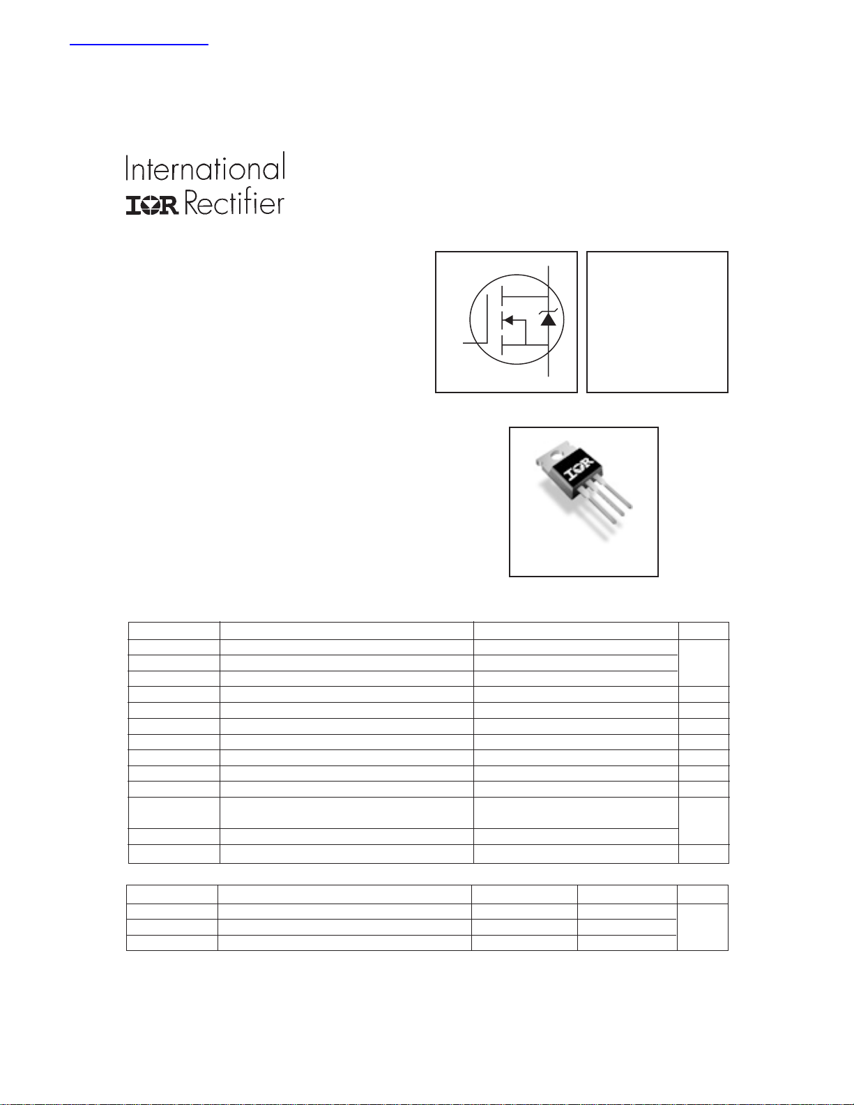
G
Description
Fifth Generation MOSFETs from International Rectifier
utilize advanced processing techniques to achieve
extremely low on-resistance per silicon area. This
benefit, combined with the fast switching speed and
ruggedized device design that HEXFET® power
MOSFETs are well known for, provides the designer
with an extremely efficient device for use in a wide
variety of applications.
The TO-220 package is universely preferred for all
commercial applications at power dissipation levels
to approximately 50 watts. The low thermal resistance
and low package cost of the TO-220 contribute to its
wide acceptance throughout the industry.
Absolute Maximum Ratings
Parameter Max. Units
ID @ TC = 25°C Continuous Drain Current, VGS @ 10V 41
ID @ TC = 100°C Continuous Drain Current, VGS @ 10V 29 A
I
DM
PD @TC = 25°C Power Dissipation 83 W
V
GS
E
AS
I
AR
E
AR
dv/dt Peak Diode Recovery dv/dt 5.0 V/ns
T
J
T
STG
Pulsed Drain Current 164
Linear Derating Factor 0.56 W/°C
Gate-to-Source Voltage ± 20 V
Single Pulse Avalanche Energy 190 mJ
Avalanche Current 25 A
Repetitive Avalanche Energy 8.3 m J
Operating Junction and -55 to + 175
Storage Temperature Range
Soldering Temperature, for 10 seconds 300 (1.6mm from case )
Mounting torque, 6-32 or M3 screw
10 lbf•in (1.1N•m)
Thermal Resistance
Parameter Typ. Max. Units
R
θJC
R
θCS
R
θJA
Junction-to-Case ––– 1.8
Case-to-Sink, Flat, Greased Surface 0.50 ––– °C/W
Junction-to-Ambient ––– 62
www.irf.com 1
D
R
S
TO-220AB
V
= 55V
DSS
= 0.027Ω
DS(on)
ID = 41A
°C
11/3/99
IRF1205
PROVISIONAL
Electrical Characteristics @ TJ = 25°C (unless otherwise specified)
Parameter Min. Typ. Max. Units Conditions
V
(BR)DSS
∆V
(BR)DSS
R
DS(on)
V
GS(th)
g
fs
I
DSS
I
GSS
Q
g
Q
gs
Q
gd
t
d(on)
t
r
t
d(off)
t
f
L
D
L
S
C
iss
C
oss
C
rss
Drain-to-Source Breakdown Voltage 55 ––– ––– V VGS = 0V, ID = 250µA
/∆T
Breakdown Voltage Temp. Coefficient ––– 0.05 ––– V/°C Reference to 25°C, ID = 1mA
J
Static Drain-to-Source On-Resistance ––– ––– 0.027 Ω VGS = 10V, ID = 25A
Gate Threshold Voltage 2.0 ––– 4.0 V VDS = VGS, ID = 250µA
Forward Transconductance 13 ––– ––– S VDS = 25V, ID = 25A
Drain-to-Source Leakage Current
––– ––– 25
––– ––– 250 VDS = 44V, VGS = 0V, TJ = 150°C
Gate-to-Source Forward Leakage ––– ––– 100 VGS = 20V
Gate-to-Source Reverse Leakage ––– ––– -100
VDS = 55V, VGS = 0V
µA
nA
VGS = -20V
Total Gate Charge ––– ––– 50 ID = 25A
Gate-to-Source Charge ––– ––– 10 nC VDS = 44V
Gate-to-Drain ("Miller") Charge ––– – –– 21 VGS = 10V
Turn-On Delay Time ––– 9.9 ––– VDD = 28V
Rise Time ––– 44 ––– ID = 25A
Turn-Off Delay Time ––– 34 ––– RG = 9.1Ω
ns
Fall Time ––– 35 ––– RD = 1.1Ω
Internal Drain Inductance
Internal Source Inductance ––– –––
––– –––
4.5
7.5
Between lead,
6mm (0.25in.)
nH
from package
and center of die contact
Input Capacitance ––– 1200 ––– VGS = 0V
Output Capacitance ––– 390 ––– pF VDS = 25V
Reverse Transfer Capacitance ––– 140 ––– ƒ = 1.0MHz
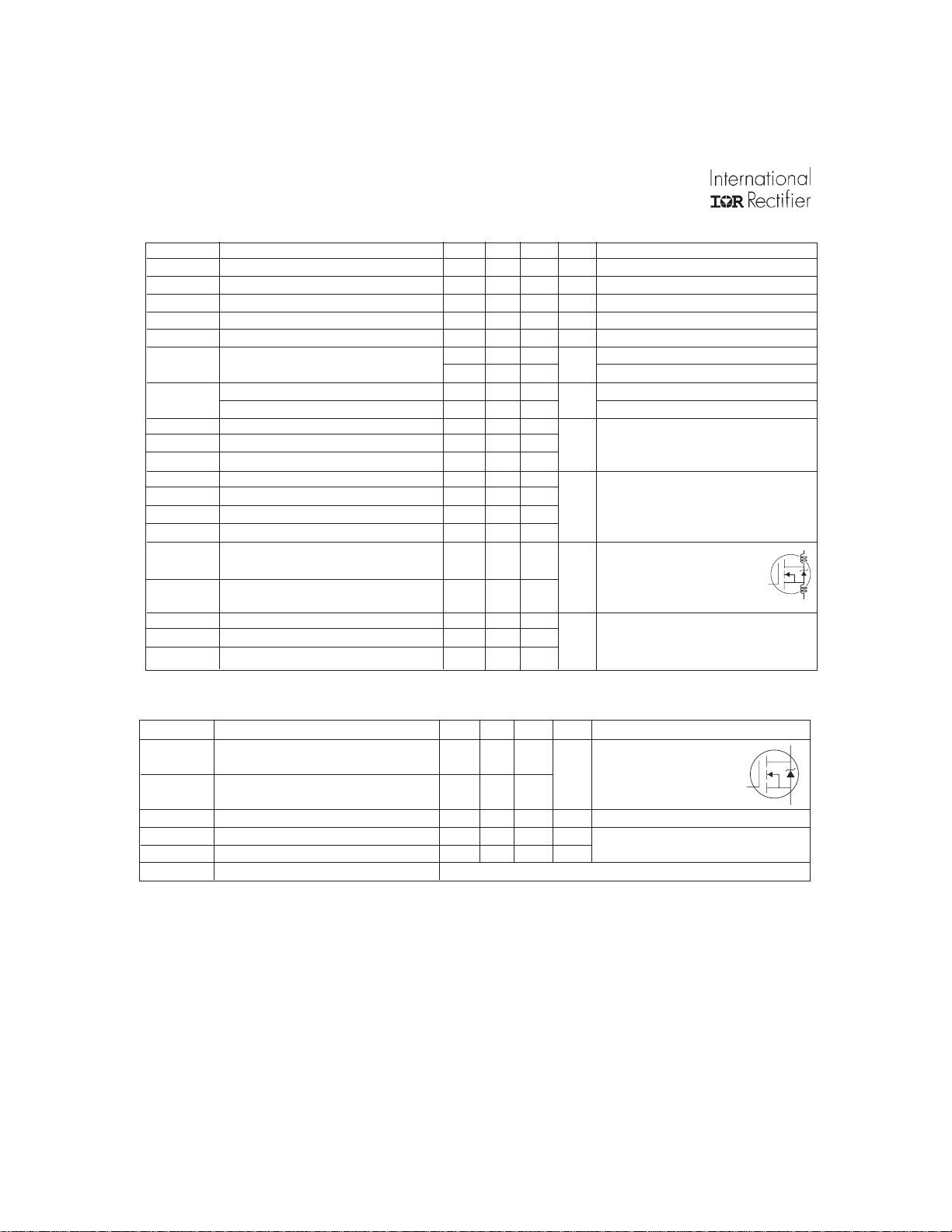
D
G
S
Source-Drain Ratings and Characteristics
Parameter Min. Typ. Max. Units Conditions
I
S
I
SM
V
SD
t
rr
Q
rr
t
on
Continuous Source Current MOSFET symbol
(Body Diode)
Pulsed Source Current integral reverse
(Body Diode)
––– –––
––– –––
41
164
showing the
A
p-n junction diode.
G
Diode Forward Voltage ––– ––– 1.3 V TJ = 25°C, IS =25A, VGS = 0V
Reverse Recovery Time ––– 63 94 ns TJ = 25°C, IF = 25A
Reverse RecoveryCharge 140 210 nC di/dt = 100A/µs
Forward Turn-On Time Intrinsic turn-on time is negligible (turn-on is dominated by LS+LD)
Notes:
Repetitive rating; pulse width limited by
Pulse width ≤ 300µs; duty cycle ≤ 2%
max. junction temperature.
V
25V, Starting TJ = 25°C, L = 610µH
DD=
RG = 25Ω, I
I
≤25A, di/dt ≤ 220A/µs, V
SD
AS
= 25A
DD
≤ V
(BR)DSS
Calculated continuous current based on maximum allowable junction
temperature: Package limitation current = 20A
,
Use IRFR/U1205 Data and Test conditons.
TJ ≤ 175°C
2 www.irf.com
D
S

TO-220AB Package Outline
A
Dimensions are shown in millimeters (inches)
PROVISIONAL
IRF1205
10.54 (.415)
2.87 (.113)
2.62 (.103)
15.24 (.600)
14.84 (.584)
14.09 (.555)
13.47 (.530)
1.40 (.055)
3X
1.15 (.045)
2.54 (.100)
NOTES:
1 DIMENSIONING & TOLERANCING PER ANSI Y14.5M, 1982. 3 OUTLINE CONFORMS TO JEDEC OUTLINE TO-220AB.
2 CO NTRO LLING DIM EN S IO N : IN C H 4 HEATSINK & LEAD M EA SURE ME NTS D O NOT INCLUDE BURRS.
10.29 (.405)
4
1 2 3
2X
3.78 (.149)
3.54 (.139)
- A -
6.47 (.255)
6.10 (.240)
1.15 (.045)
MIN
4.06 (.160)
3.55 (.140)
0.93 (.037)
3X
0.69 (.027)
0.3 6 (.014) M B A M
TO-220AB Part Marking Information
EXAMPLE : THIS IS AN IRF1010
W ITH A SSE MBLY
LOT CODE 9B 1 M
INTERN A TION A L
RE CTIFIER
L OGO
ASSEMBLY
LOT COD E
4.69 (.185)
4.20 (.165)
- B -
1.32 (.052)
1.22 (.048)
2.92 (.115)
2.64 (.104)
I RF1010
9246
9B 1M
LEAD AS SIGNM ENTS
1 - G ATE
2 - D RA IN
3 - S OU RC E
4 - D RA IN
0.55 (.022)
3X
0.46 (.018)
PART NUMB ER
DATE CODE
(YYWW)
YY = YE AR
WW = WEEK
WORLD HEADQUARTERS: 233 Kansas St., El Segundo, California 90245, Tel: (310) 322 3331
IR GREAT BRITAIN: Hurst Green, Oxted, Surrey RH8 9BB, UK Tel: ++ 44 1883 732020
IR CANADA: 15 Lincoln Court, Brampton, Ontario L6T3Z2, Tel: (905) 453 2200
IR GERMANY: Saalburgstrasse 157, 61350 Bad Homburg Tel: ++ 49 6172 96590
IR ITALY: Via Liguria 49, 10071 Borgaro, Torino Tel: ++ 39 11 451 0111
IR JAPAN: K&H Bldg., 2F, 30-4 Nishi-Ikebukuro 3-Chome, Toshima-Ku, Tokyo Japan 171 Tel: 81 3 3983 0086
IR SOUTHEAST ASIA: 1 Kim Seng Promenade, Great World City West Tower, 13-11, Singapore 237994 Tel: ++ 65 838 4630
IR TAIWAN:16 Fl. Suite D. 207, Sec. 2, Tun Haw South Road, Taipei, 10673, Taiwan Tel: 886-2-2377-9936
Data and specifications subject to change without notice. 11/99
www.irf.com 3
 Loading...