

InVue ED0991 User Manual

Model(s): ED0991 FCC ID: 2AFR8ED0991
Certification Exhibit
FCC ID: 2AFR8ED0991
FCC Rule Part: Part 15.517
ACS Project Number: 15-3027
Manufacturer: InVue Security
Model: ED0991
Manual
ACS Project: 15-3027 Advanced Compliance Solutions Page 1

ED0991 Module, Users Manual
Key Features
The ED0991 is a modular transceiver to meet the requirements of 47 C.F.R. § 15.212
(i) The radio elements of the ED0991 have their own shielding.
(ii) The ED0991 does not have modulation/data inputs. The modulation is generated internal and
the modulation type is fixed as BPM w/ BPSK. The data rates are fixed and set to the module via
an SPI interface to the host MCU.
(iii) The modular transmitter has its own power supply regulator.
An IEEE802.15.4-2011 UWB compliant wireless transceiver module based on DecaWave’s DW1000 IC.
Fully coherent receiver for maximum range and accuracy.
Designed to comply with FCC & ETSI UWB spectral masks
Supply voltage 2.8V to 3.6V
SPI Interface to host processor
Key Benefits
High immunity to multipath fading – allows reliable communications in high fading environments
Low power consumption allows operation from batteries for long periods*
Small physical size allows the implementation of cost-effective solutions in RTLS and WSN
Integrated antenna allows simple product implementation – no RF design required
Integration of DW1000 IC, antenna, power management and clock control simplifies design integration
Very precise location of tagged objects delivers enterprise efficiency gains and cost reductions
Long LOS and NLOS range reduces amount of infrastructure required to deploy systems
Low power consumption reduces the need to replace batteries and lowers system lifetime costs
Standards based solution (IEEE802.15.4-2011), eases proliferation
Low cost allows cost-effective implementation of solutions
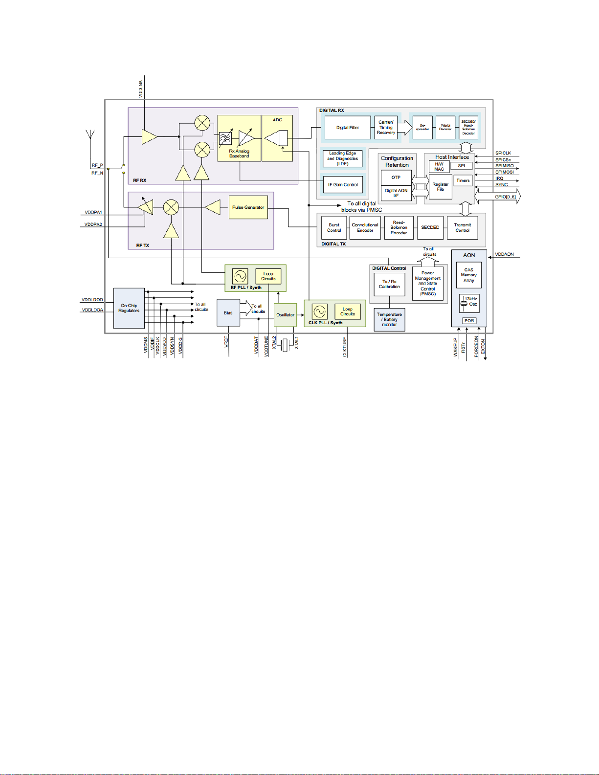
The ED0991 module interfaces to an application microcontroller via SPI bus. Physical and MAC layer functionality
are accessed via the SPI bus, through addressable registers as well as execution commands. Data received or to be
transmitted are also accessed through the SPI bus and are implemented as a FIFO register (64 bytes each for TX
and RX). To transmit, a frame of data is placed in the FIFO, this may include a destination address. A transmit
command is given, which will transmit the data according to the initial setup of the registers. To receive data a
receive command is given, which will listen for a transmission and when one occurs put the received frame in the
FIFO. When neither transmit nor receive is required the device can enter either an Idle mode, from which it can
quickly re-enter receive or transmit mode or it can enter a low power sleep mode, from which a crystal startup is
also required prior to transmit or receive operation.
A block diagram is given for the ED0991 module in Figure 1.
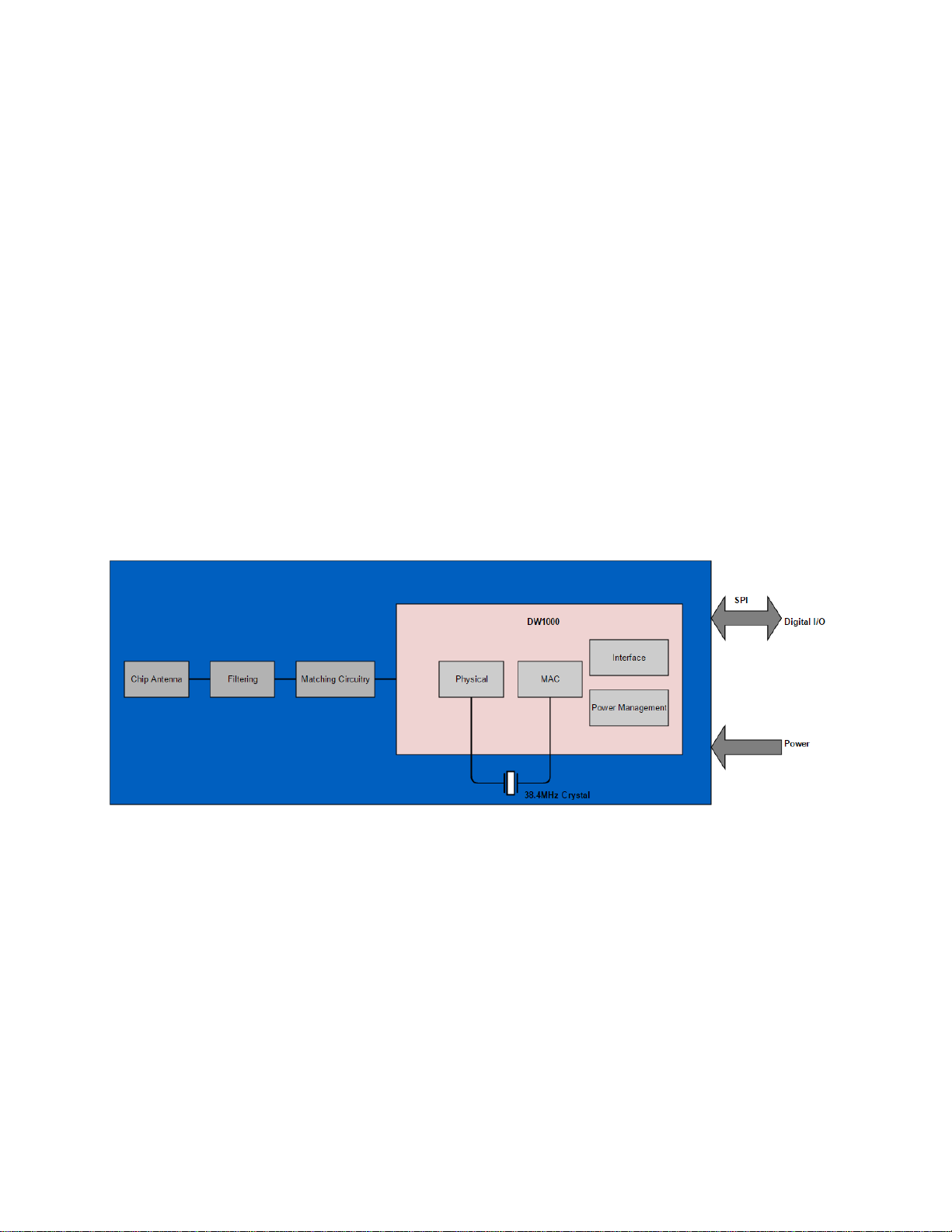
Figure 1
Antenna
The antenna couples energy between the air and the module. The ED0991 module has an integrated antenna that
is near omni-directional. Note that the end radiation pattern depend not only on the antenna, but also the ground
plane, enclosure and installation environment.
Matching
The matching provides the correct loading of the transmit amplifier to achieve the highest output
power as well as the correct loading for the receive LNA to achieve the best sensitivity.
Physical
The physical layer provides conversions between data, symbol and RF signal.
MAC
The MAC layer is part of the Logical Link Layer and provides frame handling, addressing and
medium access services.
Microcontroller Interface
The microcontroller interface exposes registers and commands for the physical and MAC layers
to a microcontroller.
Power Management
Power management ensures a stable supply for the internal functions as well as providing means
for a low power sleep mode, in which most of the transceiver is power off.
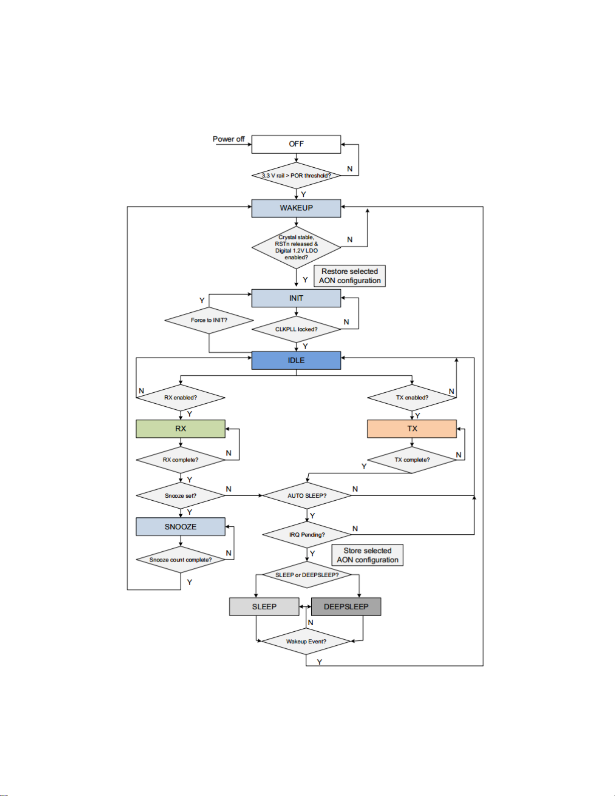
Typical Flow
After initial setup of registers for desired behavior, the normal operation flow diagram is shown in. In applications
of infrequent data transmissions the transceiver would be in SLEEP mode to save power (<100nA). From there it
would be woken up and enter WAKEUP mode. As part of the wake up process the crystal oscillator is started
(~4ms) and the digital microcontroller interface is powered up. Before transmit or receive the frequency
synthesizer needs to be started RSTn and having been powered off (or idle for a while) the control loop of the
VCO/PLL needs to be calibrated INIT. A data frame is loaded into the transmit FIFO and the TX mode is entered. In
the TX state the DW1000 actively transmits a frame containing the contents of the transmit buffer on the
configured RF channel with the configured transmit parameters (PRF, data rate, preamble code etc.) Once the
frame transmission is complete the DW1000 may enter one of three modes depending on the programmed
configuration. After the frame transmission is complete the DW1000 will return to the IDLE state unless the
ATXSLP bit is set (in Sub-Register 0x36:04 – PMSC_CTRL1) in which case the DW1000 will enter the SLEEP or
DEEPSLEEP state automatically, (as long as no host interrupts are pending). When transmit is complete RX mode is
entered to either hunting for preamble or (once it has detected preamble) actively receiving preamble searching
for SFD, and subsequently receiving the PHR, decoding it and receiving the data part of the frame. In the RX state,
the RF synthesizer and all RX blocks are active. After an event that ends the reception, (either a good frame RX, or
some error or timeout event that aborts reception) the DW1000 will return to the IDLE state unless the ARXSLP bit
is set (in Sub-Register 0x36:04 – PMSC_CTRL1) in which case the DW1000 will enter the SLEEP or DEEPSLEEP state
automatically (as long as no host interrupts are pending).

Contents
Key Features .................................................................................................................................................. 1
Key Benefits ................................................................................................................................................... 1
Antenna ......................................................................................................................................................... 2
1. Overview ............................................................................................................................................... 5
1.1. ED0991 Functional Description ..................................................................................................... 6
1.2. ED0991 Power Up ......................................................................................................................... 6
1.3. SPI Host Interface .......................................................................................................................... 7
1.3.1. SPI Signal Timing ....................................................................................................................... 7
1.4. GPIO .............................................................................................................................................. 8
1.5. Always-On Memory (AON) ............................................................................................................ 9
1.6. One Time Programmable Memory ............................................................................................... 9
1.7. Interrupts and Device Status......................................................................................................... 9
1.8. MAC ............................................................................................................................................... 9
1.9. External Synchronization .............................................................................................................. 9
2. ED0991 Pin Connections ....................................................................................................................... 9
2.1. Pin Numbering ............................................................................................................................ 10
3.1. Nominal Operating Conditions ................................................................................................... 12
3.2. DC Characteristics ....................................................................................................................... 13
3.3. Receiver AC Characteristics ......................................................................................................... 13
3.4. Transmitter AC Characteristics ................................................................................................... 14
3.5. Temperature and Voltage Monitor ............................................................................................. 14
3.6. Antenna ....................................................................................................................................... 14
3.7. Absolute Maximum Ratings ........................................................................................................ 15
4. References .......................................................................................................................................... 15
5. Regulatory Approvals and Restrictions ............................................................................................... 15
1. Overview
The ED0991 module is an IEEE 802.15.4-2011 UWB implementation. RF components, Decawave DW1000 UWB
transceiver, and other components reside on-module. ED0991 enables cost effective and reduced complexity
integration of UWB communications and ranging features, greatly accelerating design implementation.
 Loading...