

Page 1
®
X9C102, X9C103, X9C104, X9C503
Data Sheet December 20, 2006
Digitally Controlled Potentiometer
(XDCP™)
FEATURES
• Solid-state potentiometer
• 3-wire serial interface
• 100 wiper tap points
—Wiper position stored in nonvolatile memory
and recalled on power-up
• 99 resistive elements
—Temperature compensated
—End to end resistance, ±20%
—Terminal voltages, ±5V
• Low power CMOS
—V
= 5V
CC
—Active current, 3mA max.
—Standby current, 750µA max.
• High reliability
—Endurance, 100,000 data changes per bit
—Register data retention, 100 years
• X9C102 = 1kΩ
• X9C103 = 10kΩ
• X9C503 = 50kΩ
• X9C104 = 100kΩ
• Packages
—8 Ld SOIC and 8 Ld PDIP
• Pb-free plus anneal available (RoHS compliant)
FN8222.1
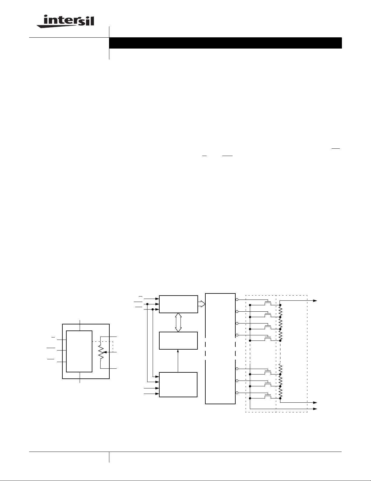
DESCRIPTION
The X9Cxxx are Intersil digitally controlled (XDCP)
potentiometers. The device consists of a resis tor
array, wiper switches, a control section, and nonvola-
tile memory. The wiper position is controlled by a
three-wire interface.
The potentiometer is implemented by a resistor array
composed of 99 resistive elements and a wiper switch-
ing network. Between each element and at either end
are tap points accessible to the wiper terminal. The
position of the wiper element is controlled by the CS
U/D
, and INC inputs. The position of the wiper can be
stored in nonvolatile memory and then be recalled
upon a subsequent power-up operation.
The device can be used as a three-terminal potentiom-
eter or as a two-terminal variable resistor in a wide
variety of applications including:
– control
– parameter adjustments
– signal processing
,
BLOCK DIAGRAM
(Supply Voltage)
V
CC
Up/Down
(U/D
)
Increment
Device
Select
(INC
(CS
)
)
Control
and
Memory
VSS (Ground)
General
U/D
INC
CS
VH/R
H
RW/V
W
VL/R
L
V
CC
GND
1
7-Bit
Up/Down
Counter
7-Bit
Nonvolatile
Memory
Store and
Recall
Control
Circuitry
CAUTION: These devices are sensitive to electrostatic discharge; follow proper IC Handling Procedures.
1-888-INTERSIL or 1-888-468-3774
XDCP is a trademark of Intersil Americas Inc. Copyright Intersil Americas Inc. 2005, 2006. All Rights Reserved
99
98
97
96
One
of
One-
Hundred
Decoder
2
1
0
Detailed
| Intersil (and design) is a registered trademark of Intersil Americas Inc.
All other trademarks mentioned are the property of their respective owners.
Transfer
Gates
Resistor
Array
RH/V
R
L/VL
RW/V
H
W
Page 2

2
Page 3
X9C102, X9C103, X9C104, X9C503
PIN DESCRIPTIONS
Pin Symbol Brief Description
1INCIncrement . The INC input is negative-edge triggered. Toggling INC will move the wiper and either
increment or decrement the counter in the direction indicated by the logic level on the U/D
2U/D
Up/Down. The U/D input controls the direction of the wiper movement and whether the cou nter
is incremented or decremented.
3R
H/VH
RH/VH. The high (V
) terminals of the X9C102/103/104/503 are equivalent to the fixed
H/RH
terminals of a mechanical potentiometer. The minimum voltage is -5V and the maximum is +5V.
The terminology of V
relation to wiper movement dire ction selected by the U/D
and VL/RL references the relative position of the terminal in
H/RH
input and not the voltage potential on
the terminal.
4 V
5 V
SS
W/RW
V
SS
VW/R
VW/RW is the wiper terminal, and is equivalent to the movable terminal of a mechanica l
W.
po te nti om et er . T he po sit io n o f t he wi per wi th in th e a rr ay i s d et er mi ne d b y th e c on tr ol inputs. The
wiper terminal series resistance is typically 40Ω.
6 R
/V
L
RL/V
L
. The low (V
L
terminals of a mechanical potentiometer. The minimum voltage is -5V and the maximum is +5V.
The terminology of V
relation to wiper movement dire ction selected by the U/D
) terminals of the X9C102/103/1 04/503 are equivalent to the fixed
L/RL
and VL/RL references the relative position of the terminal in
H/RH
input and not the voltage potential on
the terminal.
7CSCS. The device is selected when the CS input is LOW. The current counter value is stored in
nonvolatile memory when CS
is returned HIGH while the INC input is also HIGH. After the store op-
eration is complete the X9C102/103/104/503 device will be placed in the low power standby mode
until the device is selected once again.
8 V
CC
V
CC
input.
3
FN8222.1
December 20, 2006
Page 4
X9C102, X9C103, X9C104, X9C503
ABSOLUTE MAXIMUM RATINGS
Temperature under bias .................... -65°C to +135°C
Storage temperature ......................... -65°C to +150°C
Voltage on CS
, INC, U/D and V
CC
with respect to VSS.................................. -1V to +7V
Voltage on V
H/RH
and VL/R
L
referenced to VSS................................... -8V to +8V
ΔV = |V
H/RH
- VL/RL|
X9C102 ....................................... ........................ 4V
X9C103, X9C503, and X9C104 ......................... 10V
Lead temperature (soldering, 10 seconds)...... +300°C
I
(10 seconds) ..................... ............................ 8. 8mA
W
Power rating X9C102 ......... ............................... 16mW
Power rating X9C103/104/503 ........ .................. 10mW
RECOMMENDED OPERATING CONDITIONS
Temperature Min. Max.
Commercial 0°C +70°C
Industrial -40°C +85°C
COMMENT
Stresses above those listed under “Absolute Maximum
Ratings” may cause permanent damage to the device.
This is a stress rating only; functional operation of the
device (at these or any other conditions above those
listed in the operational sections of this specification) i s
not implied. Exposure to absolute maximum rating
conditions for extended periods may affect device reliability.
Supply Voltage (VCC)
Limits
X9C102/103/104/503 5V ±10%
POTENTIOMETER CHARACTERISTICS (Over recommended operating conditions unless otherwise stated.)
Limits
Symbol Parameter
R
TOTAL
V
VH/RH
V
VL/RL
R
I
W
W
End to end resistance variation -20 +20 %
VH terminal voltage -5 +5 V
VL terminal voltage -5 +5 V
Wiper current -4.4 4.4 mA
Wiper resistance 40 100 Ω Wiper Current = ±1mA
(5)
Noise
-120 dBV Ref. 1kHz
Unit Test Conditions/NotesMin. Typ. Max.
Resolution 1 %
(2)
(1)
-1 +1 MI
-0.2 +0.2 MI
Absolute linearity
Relative linearity
RTOTAL temperature coefficient ±300
RTOTAL temperature coefficient ±600
(5)
(5)
(3)
(3)
V
W(n)(actual)
V
W(n + 1)(actual)
- V
W(n)(expected)
- [V
ppm/°C X9C103/503/104
ppm/°C X9C102
W(n) + MI
Ratiometric temperature coefficient ±20 ppm/°C
C
H/CL/CW
(5)
Not es: (1 ) Absolute linearity is utilized to determine actual wiper voltage versus expected voltage = [V
(2) Relative linearity is a measure of the error in step size between taps = V
(3) 1 MI = Minimum Increment = R
(4) Typical values are for T
(5) This parameter is not 100% tested.
Potentiometer capacitances 10/10/25 pF See Circuit #3, Macro Model
/99
TOT
= +25°C and nominal supply voltage.
A
W(n + 1)
- [V
W(n)(actual)
W(n) + MI
- V
W(n)(expected )
] = +0.2 MI.
] = ±1 MI Maximum.
]
4
FN8222.1
December 20, 2006
Page 5

X9C102, X9C103, X9C104, X9C503
D.C. OPERATING CHARACTERISTICS (Over recommended operating conditions unless otherwise specified.)
Limits
(4)
Symbol Parameter
I
I
CC
SB
I
VCC active current 1 3 mA CS = VIL, U/D = VIL or VIH and
Standby supply current 200 750 µA CS = VCC - 0.3V, U/D and INC = VSS
CS, INC, U/D input leakage
LI
current
V
CS, INC, U/D input HIGH
IH
voltage
V
CS, INC, U/D input LOW
IL
voltage
(5)
C
IN
CS, INC, U/D input
capacitance
ENDURANCE AND DATA RETENTION
Parameter Min. Unit
Minimum endurance 100,000 Data changes per bit per register
Data retention 100 years
2V
10 pF VCC = 5V, VIN = VSS, TA = 25°C, f = 1MHz
Max.
Unit Test ConditionsMin. Typ.
= 0.4V to 2.4V @ max. t
INC
CC
-0.3V
or V
±10 µA VIN = VSS to V
0.8 V
CYC
CC
Test Circuit #1 Test Circuit #2 Test Circuit #3
VR/R
H
V
S
VL/R
Test Point
VW/R
W
L
VH/R
VL/R
H
L
V
W/RW
Test Point
Force
Current
R
L
C
L
10pF
A.C. CONDITIONS OF TEST
Input pulse levels 0V to 3V
Input rise and fall times 10ns
Input reference levels 1.5V
Macro Model
R
TOTAL
C
H
C
W
25pF
R
W
10pF
R
H
5
FN8222.1
December 20, 2006
Page 6

A.C. OPERATING CHARACTERISTICS (Over recommended operating conditions unless otherwise specified)
Limits
Symbol Parameter
t
Cl
t
lD
t
DI
t
lL
t
lH
t
lC
t
CPH
t
CPH
(5)
t
IW
t
CYC
(5)
t
t
,
R
F
(5)
t
PU
t
V
R
CC
CS to INC setup 100 ns
INC HIGH to U/D change 100 ns
U/D to INC setup 2.9 µs
INC LOW period 1 µs
INC HIGH period 1 µs
INC inactive to CS inactive 1 µs
CS deselect time (STORE) 20 ms
CS deselect time (NO STORE) 100 ns
INC to V
change 100 µs
W/RW
INC cycle time 2 µs
INC input rise and fall time 500 µs
Power-up to wiper stable 500 µs
(5)
V
power-up rate 0.2 50 V/ms
CC
(6)
Max.
UnitMin. Typ.
POWER-UP AND DOWN REQUIREMENTS
At all times, voltages on the potentiometer pins must be less than ±V
tile memory is not in effect until the V
supply reaches its final value. The VCC ramp rate spec is always in effect.
CC
. The recall of the wiper position from nonvola-
CC
A.C. TIMING
CS
t
CYC
t
CI
INC
U/D
V
W
Notes: (6) Typical values ar e for TA = 25°C and nominal supply voltage.
(7) This parameter is periodically sampled and not 100% tested.
(8) MI in the A.C. timing diagram refers to the minimum incremental change in the V
t
IW
t
IL
t
ID
t
IH
t
IC
t
DI
(8)
MI
t
CPH
90% 90%
10%
t
F
output due to a change in the wiper position.
W
t
R
6
FN8222.1
December 20, 2006
Page 7

X9C102, X9C103, X9C104, X9C503
DETAILED PIN DESCRIPTIONS
R
and RL/V
H/VH
L
The high (VH/RH) and low (VL/RL) terminals of the
X9C102/103/104/503 are equivalent to the fixed termi-
nals of a mechanical potentiometer. The minimum
voltage is -5V and the maximum is +5V. The terminol-
ogy of V
and VL/RL references the relative position
H/RH
of the terminal in relation to wi per movement d irection
selected by the U/D
input and not the voltage potential
on the terminal.
R
/V
W
W
VW/RW is the wiper terminal, and is equivalent to the
movable terminal of a mechanical potentiometer. The
position of the wiper within the array is determined by
th e c on t r o l inputs. The wiper terminal series resistance is
typically 40Ω.
Up/Down (U/D
The U/D
)
input controls the direction of the wiper move-
ment and whether the counter is incremented or dec-
remented.
Increment (INC
The INC
INC
input is negative-edge triggered. Toggling
will move the wiper and either increment or decre-
)
ment the counter in the direction indicated by the logic
level on the U/D
input.
PIN NAMES
Symbol Description
V
H
V
W/RW
V
V
V
/R
L/RL
SS
CC
H
High Terminal
Wiper Terminal
Low Terminal
Ground
Supply Voltage
U/D Up/Down Control Input
INC
CS
Increment Control Input
Chip Select Control Input
NC No Connection
PRINCIPLES OF OPERATION
There are three sections of the X9Cxxx: the input con-
trol, counter and decode section; the nonvolatile mem-
ory; and the resistor array. The input cont rol section
operates just like an up/down counter. The output of
this counter is decoded to turn on a single electronic
switch connecting a point on the resistor array to the
wiper output. Under the proper conditions the contents
of the counter can be stored in nonvola tile memory
and retained for future use. The resistor array is com-
prised of 99 individual resistors connec ted in series. At
either end of the array and between each resistor is an
electronic switch that transfers the potential at that
point to the wiper.
Chip Select (CS
The device is selected when the CS
)
input is LOW.
The current counter value is stored in nonvolatile
memory when CS
is returned HIGH while the INC
input is also HIGH. After the store operation is com-
plete the X9C102/103/104/503 device will be placed
in the low power standby mode until the device is
selected once again.
PIN CONFIGURATION
DIP/SOIC
INC
U/D
VH/R
V
SS
1
2
X9C102/103/104/503
3
H
4
V
8
CC
CS
7
VL/R
6
5
VW/R
L
W
The wiper, when at either fixed terminal, acts like its
mechanical equivalent and does not move beyond the
last position. That is, the counter does not wrap
around when clocked to either extreme.
The electronic switches on the device operate in a
“make before break” mode when the wiper changes
tap positions. If the wiper is moved several positions,
multiple taps are connected to the wiper for t
V
change). The R
W/RW
value for the device can
TOTAL
(INC to
IW
temporarily be reduced by a significant amount if the
wiper is moved several positions.
When the device is powered-down, the last wiper posi-
tion stored will be maintained in the nonvolatile mem-
ory. When power is restored, the co ntents of the
memory are recalled and the wiper is set to the value
last stored.
7
FN8222.1
December 20, 2006
Page 8

X9C102, X9C103, X9C104, X9C503
INSTRUCTIONS AND PROGRAMMING
The INC
the wiper along the resistor array. With CS
, U/D and CS inputs control the movement of
set LOW
the device is selected and enabled to respond to the
U/D
and INC inputs. HIGH to LOW transitions on INC
will increment or decrement (depending on the state of
the U/D
input) a seven-bit counter. The output of this
counter is decoded to select one of one-hundred wiper
positions along the resistive array.
The value of the counter is stored in nonv olatile m em-
ory whenever CS
transitions HIGH while the INC input
is also HIGH.
The system may select the X9Cxxx, move the wiper,
and deselect the device without having to store the lat-
est wiper position in nonvolatile memory. After the
wiper movement is performed as described above and
once the new position is reached, the system must
keep INC
LOW while taking CS HIGH. The new wiper
position will be maintained until changed by the sys-
tem or until a power-down/up cycle recalled the previ-
ously stored data.
This procedure allows the system to always power-up
to a preset value stored in nonvolatile memory; then
during system operation minor adjustments could be
made. The adjustments might be based on user pref-
erence: system parameter changes due to tempera-
ture drift, etc...
MODE SELECTION
INC U/D Mode
CS
L H Wiper Up
L L Wiper Down
H X Store Wiper Position
H X X Standby Current
L X No Store, Return to Standby
L H Wiper Up (not recommended)
L L Wiper Down (not recommended)
SYMBOL TABLE
WAVEFORM INPUTS OUTPUTS
Must be
steady
May change
from Low to
High
May change
from High to
Low
Don’t Care:
Changes
Allowed
N/A Center Line
Will be
steady
Will change
from Low to
High
Will change
from High to
Low
Changing:
State Not
Known
is High
Impedance
The state of U/D
may be changed while CS remains
LOW. This allows the host system to enable the
device and then move the wiper up and down until the
proper trim is attained.
8
FN8222.1
December 20, 2006
Page 9

PERFORMANCE CHARACTERISTICS
Contact the factory for more information.
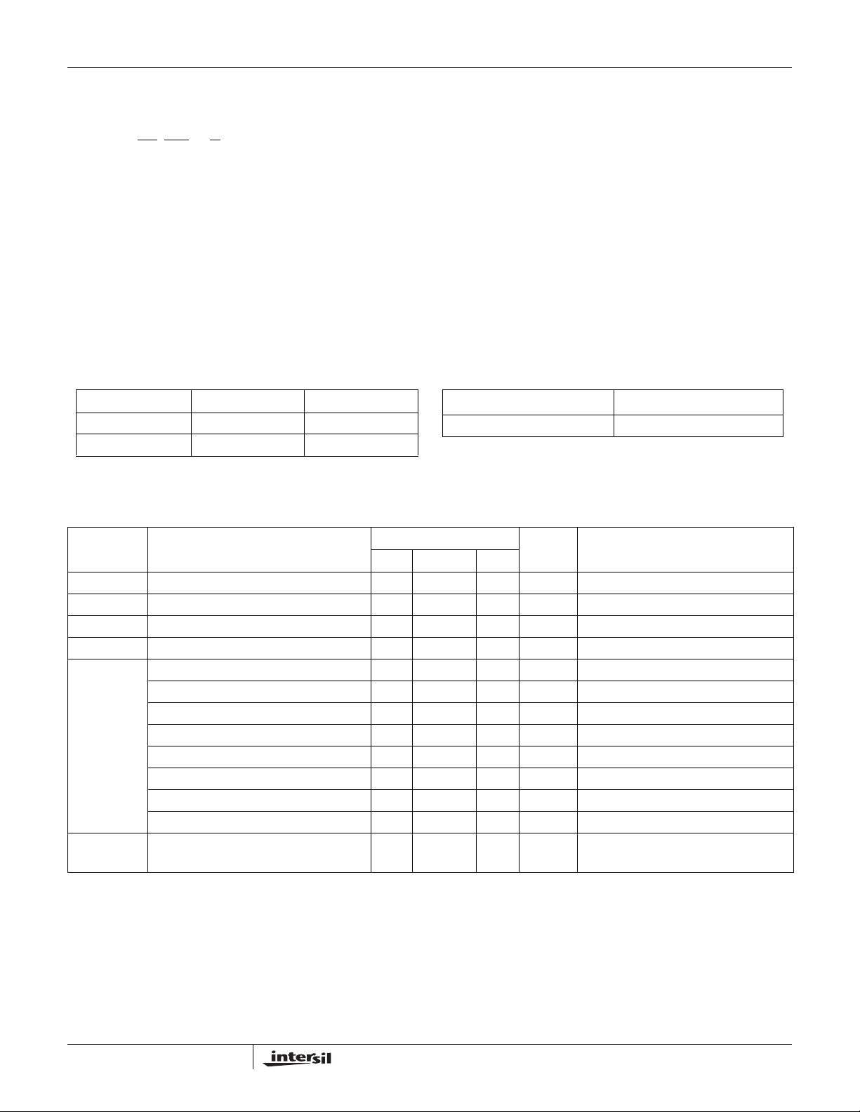
APPLICATIONS INFORMATION
Electronic digitally controlled (XCDP) potentiometers provide three powerful application advantages; (1) the variability
and reliability of a solid-state potentiometer, (2) the flexibility of computer-based digital controls, and (3) the retentivity
of nonvolatile memory used for the storage of multiple potentiometer settings or data.
Basic Configurations of Electronic Potentiometers
V
R
Basic Circuits
9
FN8222.1
December 20, 2006
Page 10

X9C102, X9C103, X9C104, X9C503
Small Outline Package Family (SO)
A
D
NN
(N/2)+1
h X 45°
PIN #1
E
C
SEATING
PLANE
0.004 C
E1
B
0.010 BM CA
I.D. MARK
1
e
0.010 BM CA
(N/2)
c
SEE DETAIL “X”
L1
H
A2
GAUGE
PLANE
A1
b
DETAIL X
L
4° ±4°
MDP0027
SMALL OUTLINE PACKAGE FAMILY (SO)
SYMBOL SO-8 SO-14
(0.150”)
A 0.068 0.068 0.068 0.104 0.104 0.104 0.104 MAX -
A1 0.006 0.006 0.006 0.007 0.007 0.007 0.007 ±0.003 -
A2 0.057 0.057 0.057 0.092 0.092 0.092 0.092 ±0.002 -
b 0.017 0.017 0 .017 0.017 0.017 0.017 0.017 ±0.003 -
c 0.009 0.0 09 0.009 0.011 0.011 0.011 0.011 ±0.0 01 -
D 0.193 0.341 0.390 0.406 0.504 0.606 0.704 ±0.004 1, 3
E 0.236 0.236 0.236 0.406 0.406 0.406 0.406 ±0.008 -
E1 0.154 0.154 0.154 0.295 0.295 0.295 0.295 ±0.004 2, 3
e 0.050 0.050 0 .050 0.050 0.050 0.050 0.050 Basic -
L 0.025 0.025 0 .025 0.030 0.030 0.030 0.030 ±0.009 -
L1 0.041 0.041 0.041 0.056 0.056 0.056 0.056 Basic -
h 0.013 0.013 0 .013 0.020 0.020 0.020 0.020 Reference -
N 8 14 16 16 20 24 28 Reference -
NOTES:
1. Plastic or metal protrusions of 0.006” maximum per side are not included.
2. Plastic interlead protrusions of 0.010” maximum per side are not included.
3. Dimensions “D” and “E1” are measured at Datum Plane “H”.
4. Dimensioning and tolerancing per ASME Y14.5M-1994
SO16
SO16 (0.300”)
(SOL-16)
SO20
(SOL-20)
SO24
(SOL-24)
SO28
(SOL-28) TOLERANCE NOTES
A
0.010
Rev. L 2/01
10
FN8222.1
December 20, 2006
Page 11

X9C102, X9C103, X9C104, X9C503
Plastic Dual-In-Line Packages (PDIP)
SEATING
PLANE
D
A2
A
L
L
e
b
A1
NOTE 5
c
E
eA
eB
N
PIN #1
E1
INDEX
12 N/2
b2
MDP0031
PLASTIC DUAL-IN-LINE PACKAGE
SYMBOL PDIP8 PDIP14 PDIP16 PDIP18 PDIP20 TOLERANCE NOTES
A 0.210 0.210 0.210 0.210 0.210 MAX
A1 0.015 0.015 0.015 0.015 0.015 MIN
A2 0.130 0.130 0.130 0.130 0.130 ±0.005
b 0.018 0.018 0.018 0.018 0.018 ±0.002
b2 0.060 0.060 0.060 0.060 0.060 +0.010/-0.015
c 0.010 0.010 0.010 0.010 0.010 +0.004/-0.002
D 0.375 0.750 0.750 0.890 1.020 ±0.010 1
E 0.310 0.310 0.310 0.310 0.310 +0.015/-0.010
E1 0.250 0.250 0.250 0.250 0.250 ±0.005 2
e 0.100 0.100 0.100 0.100 0.100 Basic
eA 0.300 0.300 0.300 0.300 0.300 Basic
eB 0.345 0.345 0.345 0.345 0.345 ±0.025
L 0.125 0.125 0.125 0.125 0.125 ±0.010
N 8 14 16 18 20 Reference
NOTES:
1. Plastic or metal protrusions of 0.010” maximum per side are not included.
2. Plastic interlead protrusions of 0.010” maximum per side are not included.
3. Dimensions E and eA are measured with the leads constrained perpe ndicular to the seating plane.
4. Dimension eB is measured with the lead tips unconstrained.
5. 8 and 16 lead packages have half end-leads as shown.
Rev. B 2/99
All Intersil U.S. products are manufactured, assembled and tested utilizing ISO9000 quality systems.
Intersil Corporation’s quality certifications can be viewed at www.intersil.com/design/quality
Intersil products are sold by description only. Intersil Corporation reserves the right to make changes in circuit design, software and/or specifications at any time without
notice. Accordingly, the reader is cautioned to verify that data sheets are current before placing orders. Information furnished by Intersil is believed to be accurate and
reliable. However, no responsibility is assumed by Intersil or its subsidiaries for its use; nor for any infringements of patents or other rights of third parties which may result
from its use. No license is granted by implicat ion or oth erwise u nde r any p a tent or p at ent r ights of Intersil or its subsidiari es.
For information regarding Intersil Corporation and its products, see www.intersil.com
11
FN8222.1
December 20, 2006
 Loading...