

S
www.BDTIC.com/Intersil
N
IG
ES
®
E
D
N
E
M
M
O
C
E
R
T
O
N
SIB
S
O
P
B
U
S
E
L
X
R
O
F
D
U
IT
T
S
2
1
0
6
9
D
W
E
N
R
P
E
T
T
C
U
D
O
Data Sheet November 11, 2005
X9530
FN8211.1
Temperature Compensated Laser Diode
Controller
FEATURES
• Compatible with Popular Fiber Optic Module
Specifications such as Xenpak, SFF, SFP, and
GBIC
• Package
—14 Ld TSSOP
• Two Programmable Current Generators
—±1.6 mA max.
—8-bit (256 Step) Resolution
• Integrated 6 bit A/D Converter
• Temperature Compensation
—Internal or External Sensor
—-40°C to +100°C Range
—2.2°C/step Resolution
—EEPROM Look-up Tables
• Hot Pluggable
• 2176-bit EEPROM
—17 Pages
—16 Bytes per Page
• Write Protection Circuitry
—Intersil BlockLock™
—Logic Controlled Protection
—2-wire Bus with 3 Slave Address Bits
• 3V to 5.5V, Single Supply Operation
• Pb-Free Plus Anneal Available (RoHS Compliant)
LASER DIODE BIAS CONTROL APPLICATIONS
• SONET and SDH Transmission Systems
• 1G and 10G Ethernet, and Fibre Channel Laser
Diode Driver Circuits
DESCRIPTION
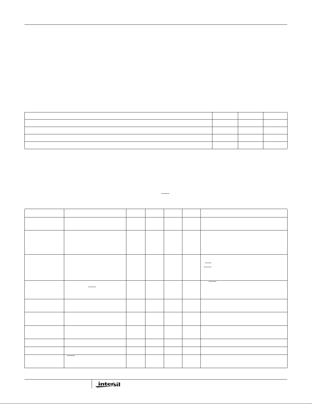
The X9530 is a highly integrated laser diode bias
controller which incorporates two digitally controlled
Programmable Current Generators, temperature
compensation with dedicated look-up tables, and
supplementary EEPROM array. All functions of the
device are controlled via a 2-wire digital serial interface.
Two temperature compensated Programmable Current
Generators, vary the output current with temperature
according to the contents of the associated nonvolatile
look-up table. The look-up table may be programmed
with arbitrary data by the user, via the 2-wire serial port,
and either an internal or external temperature sensor
may be used to control the output current response.
These temperature compensated pro-grammable
currents maybe used to control the modulation current
and the bias current of a laser diode.
The integrated General Purpose EEPROM is included
for product data storage and can be used for transceiver
module information storage in laser diode applications.
PART
NUMBER
X9530V14I* X9530V -40 to 100 14 LEAD TSSOP
X9530V14IZ*
(Note)
*Add "T1" suffix for tape and reel.
NOTE: Intersil Pb-free plus anneal products employ special Pb-free
material sets; molding compounds/die attach materials and 100%
matte tin plate termination finish, which are RoHS compliant and
compatible with both SnPb and Pb-free soldering operations. Intersil
Pb-free products are MSL classified at Pb-free peak reflow
temperatures that meet or exceed the Pb-free requirements of
IPC/JEDEC J STD-020.
PART
MARKING
X9530V Z -40 to 100 14 LEAD TSSOP
TEMP RANGE
(°C) PACKAGE
(Pb-free)
PIN CONFIGURATION
1
A0
A1
A2
Vcc
WP
SCL
SDA
2
3
4
5
6
7
14
13
12
11
10
9
8
I2
VRef
VSense
Vss
R2
R1
I1
TSSOP 14L
1
CAUTION: These devices are sensitive to electrostatic discharge; follow proper IC Handling Procedures.
1-888-INTERSIL or 1-888-468-3774
| Intersil (and design) is a registered trademark of Intersil Americas Inc.
All other trademarks mentioned are the property of their respective owners.
Copyright Intersil Americas Inc. 2005. All Rights Reserved
TYPICAL APPLICATION
www.BDTIC.com/Intersil
High Speed
Data Input
X9530
GBIC / SFP / XFP Module
V
CC
MPDLD
MOD_DEF
MOD_DEF
(0)
(1)
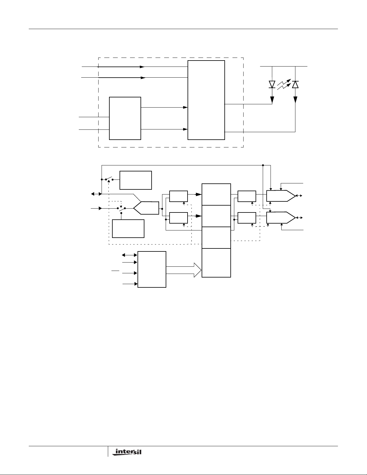
BLOCK DIAGRAM
VSense
X9530
SDA
SCK
Reference
Temperature
Sensor
SDA
SCL
WP
I
1
I
2
Voltage
I
MODSET
I
PINSET/IBIASSET
ADC
2-Wire
Interface
Mux
Mux
Laser
Diode
Driver
Circuit
Look-up
Table 2
Look-up
Table 1
Control
& Status
General
Purpose
Memory
Mux
Mux
I
LD
DAC 2
DAC 1
I
MON
R2
I2VRef
I1
R1
A2, A1, A0
DEVICE DESCRIPTION
The X9530 combines two Programmable Current
Generators, and integrated EEPROM with Block
Lock™ protection, in one package. The
Programmable Current Generators are ideal for use in
fiber optic Modulation Current require temperature
control. The combination of the X9530 functionality
and Intersil’s Chip-Scale package lowers system cost,
increases reliability, and reduces board space
requirements.
Two on-chip Programmable Current Generators may
be independently programmed to either sink or source
current. The maximum current generated is
determined by using an externally connected
programming resistor, or by selecting one of three
2
predefined values. Both current generators have a
maximum output of ±1.6 mA, and may be controlled to
an absolute resolution of 0.39% (256 steps / 8 bit).
Both current generators may be driven using an onboard temperature sensor, an external sensor, or
Control Registers. The internal temperature sensor
operates over a very broad temperature range (-40
to +100
°C). The sensor output (internal or external)
°C
drives a 6-bit A/D converter, whose output selects one
of 64 bytes from each nonvolatile look-up table (LUT).
The contents of the selected LUT row (8-bit wide)
drives the input of an 8-bit D/A converter, which
generates the output current.
All control and setup parameters of the X9530,
including the look-up tables, are programmable via the
2-wire serial port.
FN8211.1
November 11, 2005
X9530
www.BDTIC.com/Intersil
The general purpose memory portion of the device is a
CMOS serial EEPROM array with Intersil’s Block
TM
Lock
protection. This memory may be used to store
fiber optic module manufacturing data, serial numbers,
or various other system parameters.
The EEPROM array is internally organized as 272 x 8
bits with 16-Byte pages, and utilizes Intersil’s
proprietary Direct Write™ cells, providing a minimum
endurance of 100,000 Page Write cycles and a
minimum data retention of 100 years.
PIN ASSIGNMENTS
TSSOP
Pin
1A0Device Address Select Pin 0. This pin determines the LSB of the device address
2A1Device Address Select Pin 1. This pin determines the intermediate bit of the device address re-
3A2Device Address Select Pin 2. This pin determines the MSB of the device address required to
4VccSupply Voltage.
5WP
6SCLSerial Clock. This is a TTL compatible input pin. This input is the 2-wire interface clock controlling
7SDASerial Data. This pin is the 2-wire interface data into or out of the device. It is TTL
8I1Current Generator 1 Output. This pin sinks or sources current. The magnitude and direction of
9R1Current Programming Resistor 1. A resistor between this pin and Vss can set the maximum
10 R2 Current Programming Resistor 2. A resistor between this pin and Vss can set the maximum
11 Vss Ground.
12 VSense Sensor Voltage Input. This voltage input may be used to drive the input of the on-chip A/D con-
13 VRef Reference Voltage Input or Output. This pin can be configured as either an Input or an Output.
14 I2 Current Generator 2 Output. This pin sinks or sources current. The magnitude and direction of
Pin
Name Pin Description
required to communicate using the 2-wire interface. The A0 pin has an on-chip pull-down resistor.
quired to communicate using the 2-wire interface. The A1 pin has an on-chip pull-down resistor.
communicate using the 2-wire interface. The A2 pin has an on-chip pull-down resistor.
Write Protect Control Pin. This pin is a CMOS compatible input. When LOW, Write Protection
is enabled preventing any “Write” operation. When HIGH, various areas of the memory can be
protected using the Block Lock bits BL1 and BL0. The WP
which enables the Write Protection when this pin is left floating.
data input and output at the SDA pin.
compatible when used as an input, and it is Open Drain when used as an output. This pin requires
an external pull up resistor.
the current is fully programmable and adaptive. The resolution is 8 bits.
output current available at pin I1. If no resistor is used, the maximum current must be selected
using control register bits.
output current available at pin I2. If no resistor is used, the maximum current must be selected
using control register bits.
verter.
As an Input, the voltage at this pin is provided by an external source. As an Output, the voltage
at this pin is a buffered output voltage of the on-chip bandgap reference circuit. In both cases, the
voltage at this pin is the reference for the A/D
converter and the two D/A converters.
the current is fully programmable and adaptive. The resolution is 8 bits.
pin has an on-chip pull-down resistor,
3
FN8211.1
November 11, 2005
X9530
www.BDTIC.com/Intersil
PRINCIPLES OF OPERATION
CONTROL AND STATUS REGISTERS
The Control and Status Registers provide the user
with a mechanism for changing and reading the value
of various parameters of the X9530. The X9530
contains seven Control, one Status, and several
Reserved registers, each being one Byte wide (See
Figure 1). The Control registers 0 through 6 are
located at memory addresses 80h through 86h
respectively. The Status register is at memory address
87h, and the Reserved registers at memory address
88h through 8Fh.
All bits in Control register 6 always power-up to the
logic state “0”. All bits in Control registers 0 through 5
power-up to the logic state value kept in their
corresponding nonvolatile memory cells. The
nonvolatile bits of a register retain their stored values
even when the X9530 is powered down, then powered
back up. The nonvolatile bits in Control 0 through
Control 5 registers are all preprogrammed to the logic
state “0” at the factory.
Bits indicated as “Reserved” are ignored when read,
and must be written as “0”, if any Write operation is
performed to their registers.
A detailed description of the function of each of the
Control and Status register bits follows:
Control Register 0
This register is accessed by performing a Read or
Write operation to address 80h of memory.
BL1, BL0: B
ON-VOLATILE)
(N
These two bits are used to inhibit any write operation
to certain addresses within the memory array. The
protected region of memory is determined by the
values of the two bits as shown in the table below:
BL1
0 0 None (Default) None (Default)
0 1 00h to 7Fh (128 bytes)
1 0 00h to 7Fh and 90h to
1 1 00h to 7Fh and 90h to
If the user attempts to perform a write operation to a
protected region of memory, the operation is aborted
without changing any data in the array.
LOCK LOCK PROTECTION BITS
Protected Addresses
BL0
(Size)
CFh (192 bytes)
10Fh (256 bytes)
Partition of array
locked
GPM
GPM, LUT1
GPM, LUT1, LUT2
Notice that if the Write Protect (WP
X9530 is active (LOW), then any write operation to
the memory is inhibited, irrespective of the Block
Lock bit settings.
VRM: V
(N
The VRM bit configures the Voltage Reference pin
(VRef) as either an input or an output. When the VRM
bit is set to “0” (default), the voltage at pin VRef is an
output from the X9530’s internal voltage reference.
When the VRM bit is set to “1”, the voltage reference
for the VRef pin is external. See Figure 2.
ADCIN: A/D C
(NON-VOLATILE)
The ADCIN bit selects the input of the on-chip A/D
converter. When the ADCIN bit is set to “0” (default),
the output of the on-chip temperature sensor is the
input to the A/D converter. When the ADCIN bit is set
to “1”, the input to the A/D converter is the voltage at
the VSense pin. See Figure 4.
ADC
(N
When this bit is “1”, the status register at 87h is
updated after every conversion of the ADC. When this
bit is “0” (default), the status register is updated after
four consecutive conversions with the same result.
NV1234: C
TILITY MODE SELECTION BIT (NON-VOLATILE)
When the NV1234 bit is set to “0” (default), bytes
written to Control registers 1, 2, 3, and 4 are stored in
volatile cells, and their content is lost when the X9530
is powered down. When the NV1234 bit is set to “1”,
bytes written to Control registers 1, 2, 3, and 4 are
stored in both volatile and nonvolatile cells, and their
value doesn’t change when the X9530 is powered
down and powered back up. See “Writing to Control
Registers” on page 17.
I1DS: C
(N
The I1DS bit sets the polarity of Current Generator 1,
DAC1. When this bit is set to “0” (default), the Current
Generator 1 of the X9530 is configured as a Current
Source. Current Generator 1 is configured as a
Current Sink when the I1DS bit is set to “1”. See
Figure 5.
OLTAGE REFERENCE PIN MODE
ON-VOLATILE)
ONVERTER INPUT SELECT
FILTOFF: ADC FILTERING CONTROL
ON-VOLATILE)
ONTROL REGISTERS 1, 2, 3, AND 4 VOLA-
URRENT GENERATOR 1 DIRECTION SELECT BIT
ON-VOLATILE)
) input pin of the
4
FN8211.1
November 11, 2005
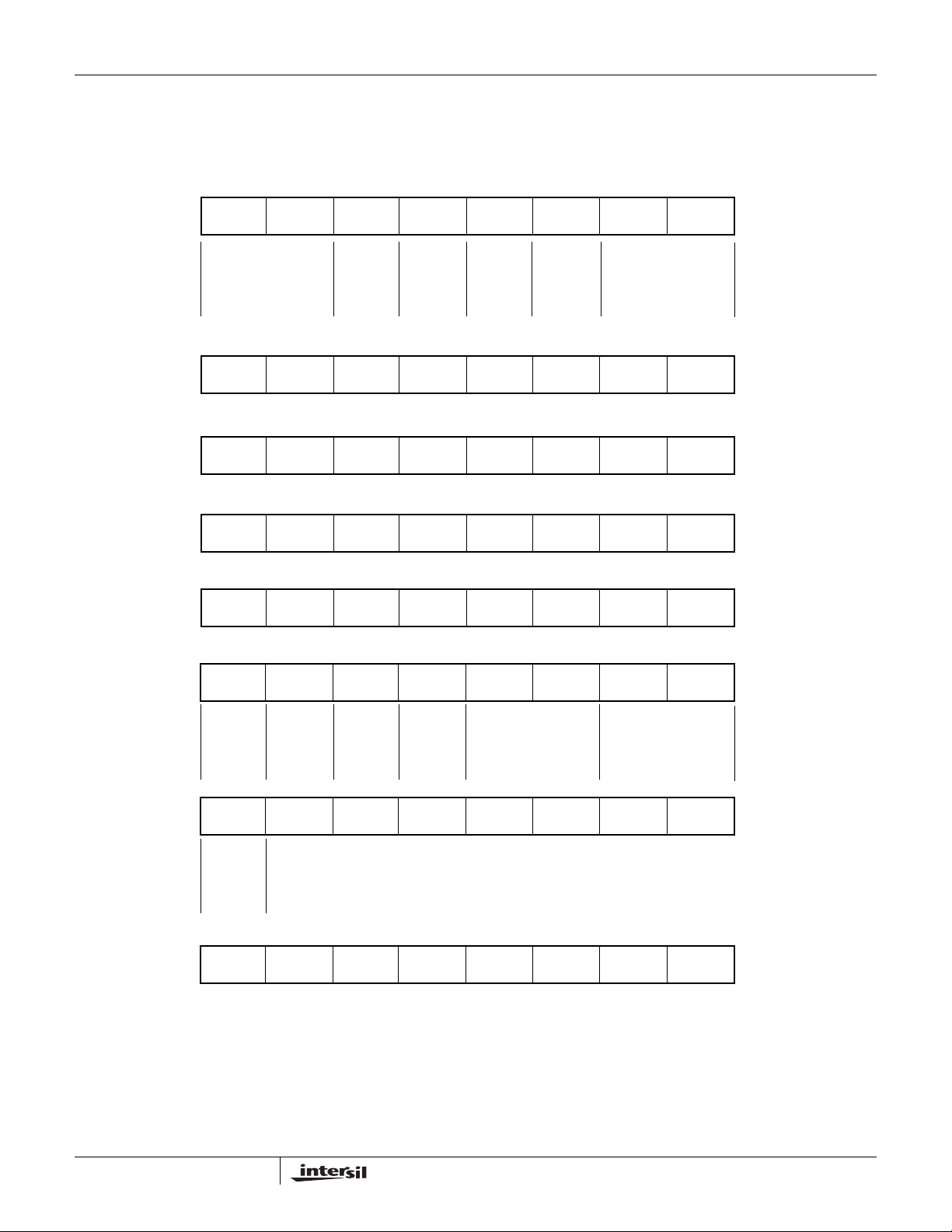
Figure 1. Control and Status Register Format
www.BDTIC.com/Intersil
X9530
Byte
Address
80h
Non-Volatile
81h
Volatile or
Non-Volatile
82h
Volatile or
Non-Volatile
83h
Volatile or
Non-Volatile
84h
Volatile or
Non-Volatile
MSB LSB
7
6
5
4
3
21
BL1 BL0I1DS NV1234I2DS ADCfiltOff ADCIN VRM
I1 and I2 Direction
0: Source
1: Sink
Control
1, 2, 3, 4
Volatility
0: Volatile
1: Non-
volatile
ADC
filtering
0: On
1: Off
ADC Input
0: Internal
1: External
Voltage Block Lock
Reference
Mode
0: Internal
1: External
00: None Locked
01: GPM Locked
10: GPM, LUT1, Locked
11: GPM, LUT1, LUT2
Locked
Direct Access to LUT1
Reserved Reserved L1DA5 L1DA4 L1DA3 L1DA2 L1DA1 L1DA0
Direct Access to LUT2
Reserved Reserved L2DA5 L2DA4 L2DA3 L2DA2 L2DA1 L2DA0
Direct Access to DAC1
D1DA7 D1DA6 D1DA5 D1DA4 D1DA3 D1DA2 D1DA1 D1DA0
Direct Access to DAC2
D2DA7 D2DA6 D2DA5 D2DA4 D2DA3 D2DA2 D2DA1 D2DA0
Register
0
Name
Control 0
Control 1
Control 2
Control 3
Control 4
85h
Non-Volatile
86h
Volatile
87h
Volatile
D2DAS L2DAS D1DAS L1DAS I2FSO1 I2FSO0 I1FSO1 I1FSO0
Direct
Access
to DAC2
0: Disabled
1: Enabled
Direct Direct Direct R2 Selection
Access
to LUT2
0: Disabled
1: Enabled
Access
to DAC1
0: Disabled 0: Disabled
1: Enabled 1: Enabled
Access
to LUT1
00: External
01: Low Internal
10: Middle Internal
11: High Internal
R1 Selection
00: External
01: Low Internal
10: Middle Internal
11: High Internal
WEL Reserved Reserved Reserved Reserved Reserved Reserved Reserved
Write
Enable
Latch
0: Write
Disabled
1: Write
Enabled
ADC Output
AD5 AD4 AD3 AD2 AD1 AD0 Reserved Reserved
Registers in byte addresses 88h through 8Fh are reserved.
Control 5
Control 6
Status
5
FN8211.1
November 11, 2005
X9530
www.BDTIC.com/Intersil
I2DS: CURRENT GENERATOR 2 DIRECTION SELECT BIT
ON-VOLATILE)
(N
The I2DS bit sets the polarity of Current Generator 2,
DAC2. When this bit is set to “0” (default), the Current
Generator 2 of the X9530 is configured as a Current
Source. Current Generator 2 is configured as a
Current Sink when the I2DS bit is set to “1”. See
Figure 5.
Control Register 1
This register is accessed by performing a Read or Write
operation to address 81h of memory. This byte’s volatility
is determined by bit NV1234 in Control register 0.
L1DA5 - L1DA0: LUT1 D
IRECT ACCESS BITS
When bit L1DAS (bit 4 in Control register 5) is set to
“1”, LUT1 is addressed by these six bits, and it is not
addressed by the output of the on-chip A/D converter.
When bit L1DAS is set to “0”, these six bits are ignored
by the X9530. See Figure 7.
A value between 00h (00
) and 3Fh (6310) may be
10
written to these register bits, to select the corresponding
row in LUT1. The written value is added to the base
address of LUT1 (90h).
Control Register 2
This register is accessed by performing a read or write
operation to address 82h of memory. This byte’s
volatility is determined by bit NV1234 in Control
register 0.
L2DA5 - L2DA0: LUT2 D
IRECT ACCESS BITS
When bit L2DAS (bit 6 in Control register 5) is set to
“1”, LUT2 is addressed by these six bits, and it is not
addressed by the output of the on-chip A/D converter.
When bit L2DAS is set to “0”, these six bits are ignored
by the X9530. See Figure 7.
A value between 00h (00
) and 3Fh (6310) may be
10
written to these register bits, to select the corresponding
row in LUT2. The written value is added to the base
address of LUT2 (D0h).
D1DA7 - D1DA0: D/A 1 D
IRECT ACCESS BITS
When bit D1DAS (bit 5 in Control register 5) is set to
“1”, the input to the D/A converter 1 is the content of
bits D1DA7 - D1DA0, and it is not a row of LUT1.
When bit D1DAS is set to “0” (default) these eight bits
are ignored by the X9530. See Figure 6.
Control Register 4
This register is accessed by performing a Read or
Write operation to address 84h of memory. This byte’s
volatility is determined by bit NV1234 in Control
register 0.
D2DA7 - D2DA0: D/A 2 D
IRECT ACCESS BITS
When bit D2DAS (bit 7 in Control register 5) is set to
“1”, the input to the D/A converter 2 is the content of
bits D2DA7 - D2DA0, and it is not a row of LUT2.
When bit D2DAS is set to “0” (default) these eight bits
are ignored by the X9530. (See Figure 6).
Control Register 5
This register is accessed by performing a Read or
Write operation to address 85h of memory.
I1FSO1 - I1FSO0: C
UTPUT SET BITS (NON-VOLATILE)
O
URRENT GENERATOR 1 FULL SCALE
These two bits are used to set the full scale output
current at the Current Generator 1 pin, I1. If both bits
are set to “0” (default), an external resistor connected
between pin R1 and Vss, determines the full scale
output current available at pin I1. The other three
options are indicated in the table below. The direction
of this current is set by bit I1DS in Control register 0.
See Figure 5.
I1FSO1 I1FSO0 I1 Full Scale Output Current
0 0 Set externally via pin R1 (Default)
01 ±0.4mA*
10 ±0.85 mA*
11 ±1.3 mA*
*No external resistor should be connected in these cases between
R1 and V
SS
.
Control Register 3
This register is accessed by performing a Read or Write
operation to address 83h of memory. This byte’s volatility
is determined by bit NV1234 in Control register 0.
6
FN8211.1
November 11, 2005
X9530
www.BDTIC.com/Intersil
I2FSO1–I2FSO0: CURRENT GENERATOR 2 FULL
CALE OUTPUT CURRENT SET BITS (NON-VOLATILE)
S
These two bits are used to set the full scale output
current at the Current Generator 2 pin, I2. If both bits
are set to “0” (default), an external resistor connected
between pin R2 and Vss, determines the full scale
output current available at pin I2. The other three
options are indicated in the table below. The direction
of this current is set by bit I2DS in Control Register 0.
I2FSO1 I2FSO0 I2 Full Scale Output Current
0 0 Set externally via pin R2 (Default)
01 ±0.4mA*
10 ±0.85 mA*
11 ±1.3 mA*
*No external resistor should be connected in these cases between
R2 and V
SS
.
L1DAS: LUT1 DIRECT ACCESS SELECT BIT (NON-
VOLATILE)
When bit L1DAS is set to “0” (default), LUT1 is
addressed by the output of the on-chip A/D converter.
When bit L1DAS is set to “1”, LUT1 is addressed by
bits L1DA5 - L1DA0.
D1DAS: D/A 1 D
VOLATILE)
IRECT ACCESS SELECT BIT (NON-
When bit D1DAS is set to “0” (default), the input to the
D/A converter 1 is a row of LUT1. When bit D1DAS is
set to “1”, that input is the content of the Control
register 3.
L2DAS: LUT2 D
VOLATILE)
IRECT ACCESS SELECT BIT (NON-
When bit L2DAS is set to “0” (default), LUT2 is
addressed by the output of the on-chip A/D converter.
When bit L2DAS is set to “1”, LUT2 is addressed by
bits L2DA5 - L2DA0.
D2DAS: D/A 2 D
VOLATILE)
IRECT ACCESS SELECT BIT (NON-
When bit D2DAS is set to “0” (default), the input to the
D/A converter 2 is a row of LUT2. When bit D2DAS is
set to “1”, that input is the content of the Control
register 4.
Control Register 6
This register is accessed by performing a Read or
Write operation to address 86h of memory.
WEL: W
RITE ENABLE LATCH (VOLATILE)
The WEL bit controls the Write Enable status of the
entire X9530 device. This bit must be set to “1” before
any other Write operation (volatile or nonvolatile).
Otherwise, any proceeding Write operation to memory
is aborted and no ACK is issued after a Data Byte.
The WEL bit is a volatile latch that powers up in the “0”
state (disabled). The WEL bit is enabled by writing
10000000
to Control register 6. Once enabled, the
2
WEL bit remains set to “1” until the X9530 is powered
down, and then up again, or until it is reset to “0” by
writing 00000000
to Control register 6.
2
A Write operation that modifies the value of the WEL
bit will not cause a change in other bits of Control
register 6.
Status Register - ADC Output
This register is accessed by performing a Read
operation to address 87h of memory.
AD5 - AD0: A/D C
ONLY)
ONVERTER OUTPUT BITS (READ
These six bits are the binary output of the on-chip A/D
converter. The output is 000000
and 111111
for full scale input.
2
for minimum input
2
7
FN8211.1
November 11, 2005
X9530
www.BDTIC.com/Intersil
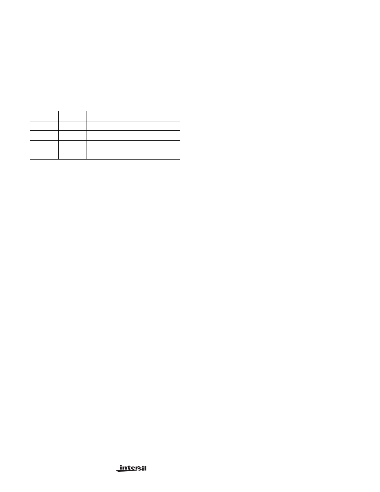
VOLTAGE REFERENCE
The voltage reference to the A/D and D/A converters
on the X9530, may be driven from the on-chip voltage
reference, or from an external source via the VRef pin.
Bit VRM in Control Register 0 selects between the two
options (See Figure 2).
The default value of VRM is “0”, which selects the
internal reference. When the internal reference is
selected, it’s output voltage is also an output at pin
VRef with a nominal value of 1.21 V. If an external
voltage reference is preferred, the VRM bit of the
Control Register 0 must be set to “1”.
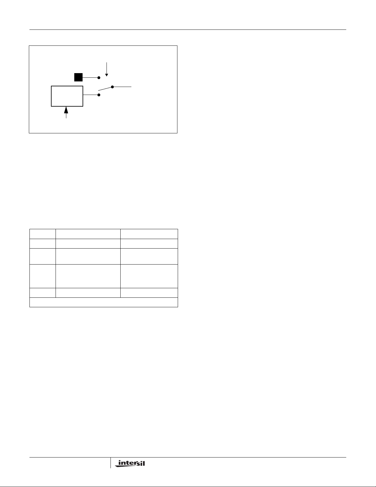
Figure 2. Voltage Reference Structure
VRM: bit 2 in Control register 0.
VRef Pin
On-chip
Voltage
Reference
A/D Converter and
D/A Converters reference
A/D CONVERTER
The X9530 contains a general purpose, on-chip, 6-bit
Analog to Digital (A/D) converter whose output is
available at the Status Register as bits AD[5:0]. By
default these output bits are used to select a row in the
look-up tables associated with the X9530’s Current
Generators. When bit ADCfiltOff is “0” (default), bits
AD[5:0] are updated each time the ADC performs four
consecutive conversions with the same exact result.
When bit ADCfiltOff is “1”, these bits are updated after
every ADC conversion.
A block diagram of the A/D converter is shown in
Figure 3. The voltage reference input (see “VOLTAGE
REFERENCE” for details), sets the maximum
amplitude of the ramp generator output. The A/D
converter input signal (see “A/D Converter Input
Select” below for details) is compared to the ramp
generator output. The control and encode logic
produces a binary encoded output, with a minimum
value of 00h (0
).
(63
10
The A/D converter input voltage range (VIN
), and a full scale output value of 3Fh
10
ADC
) is
from 0 V to V(VRef).
A/D Converter Input Select
The input signal to the A/D converter on the X9530,
may be the output of the on-chip temperature sensor,
or an external source via the VSense pin. Bit ADCIN in
Control register 0 selects between the two options
(See Figure 4). It’s default value is “0”, which selects
the internal temperature sensor.
If an external source is intended as the input to the
A/D converter, the ADCIN bit of the Control register 0
must be set to “1”.
Figure 3. A/D Converter Block Diagram
A/D Converter Input
From VRef
Ramp
Generator
8
Comparator
Conversion Reset
Clock
Control and
Encode Logic
6
A/D Converter
Output
(To LUTs
and Status
Register)
FN8211.1
November 11, 2005
X9530
www.BDTIC.com/Intersil
Figure 4. A/D Converter Input Select Structure
ADCIN: bit 3 in Control register 0.
VSense
Pin
On-chip
Temperature
Sensor
VRef
To A/D
Converter
Input
A/D Converter Range
From Figure 3 we can see that the operating range of
the A/D converter input depends on the voltage
reference. And from Figure 4 we see that the internal
temperature Sensor output also varies with the voltage
reference (VRef).
The table below summarizes the voltage range
restrictions on the VSense and VRef pins in different
configurations :
VSense and VRef ranges
VRef A/D Converter Input Ranges
Internal Internal Temp. Sensor Not Applicable
Internal VSense Pin 0 ≤ V(VSense) ≤
V(VRef)
External VSense Pin 0 ≤ V(VRef) ≤ 1.3 V
0 ≤ V(VSense) ≤
V(VRef)
External Internal Temp. Sensor Not a Valid Case
All voltages referred to Vss.
LOOK-UP TABLES
The X9530 memory array contains two 64-byte look-up
tables. One is associated to pin I1’s output current
generator and the other to pin I2’s output current
generator, through their corresponding D/A converters.
The output of each look-up table is the byte contained in
the selected row. By default these bytes are the inputs
to the D/A converters driving pins I1 and I2.
The byte address of the selected row is obtained by
adding the look-up table base address (90h for LUT1,
and D0h for LUT2) and the appropriate row selection
bits. See Figure 6.
By default the look-up table selection bits are the 6-bit
output of the A/D converter. Alternatively, the A/D
converter can be bypassed and the six row selection
bits are the six LSBs of Control Registers 1 and 2, for
the LUT1 and LUT2 respectively. The selection
between these options is illustrated in Figure 7, and
described in “I2DS: Current Generator 2 Direction Select
Bit (Non-volatile)” on page 6, and “Control Register 2”
on page 6.
CURRENT GENERATOR BLOCK
The Current Generator pins I1 and I2 are outputs of
two independent current mode D/A converters.
D/A Converter Operation
The Block Diagram for each of the D/A converters is
shown in Figure 5.
The input byte of the D/A converter selects a voltage
on the non-inverting input of an operational amplifier.
The output of the amplifier drives the gate of a FET,
whose source is connected to ground via resistor R1.
This node is also fed back to the inverting input of the
amplifier. The drain of the FET is connected to the
output current pin (I1) via a “polarity select” circuit
block.
9
FN8211.1
November 11, 2005

Figure 5. D/A Converter Block Diagram
www.BDTIC.com/Intersil
I1DS or I2DS: bits
6 or 7 in Control
register 0.
X9530
Vcc
Polarity
Select
Circuit
I1 or I2 Pin
VRef
DAC1 or
DAC2
Input byte
Voltage
Divider
I1FSO[1:0]
or I2FSO[1:0]
bits 1 and 0, or
3 and 2 in Control
register 5
Figure 6. Look-up Table (LUT) Operation
LUT2 Row
Selection bits
D0h
6
A
D
D
E
8
R
+
-
R1_High_Current or
R2_High_Current
Vss Vss
8
11
R1_Middle_Current or
LUT2
10Fh
R2_Middle_Current
…
D0h
10 01
R1 or R2 Pin
00
R1_External or R2_External
Optional external resistor
R1_Low_Current or
R2_Low_Current
Vss
D2DA[7:0] : Control register 4
8
Vss
8
D1
Out
D0
Select
D2DAS: Bit 7 of
Control register 5
DAC 2
Input Byte
D1DA[7:0] : Control register 3
LUT1 Row
Selection bits
90h
6
A
D
8
D
E
8
R
LUT1
CFh
…
90h
8
8
D1
D0
Select
10
Out
D1DAS: Bit 5 of
Control register 5
DAC 1
Input Byte
FN8211.1
November 11, 2005

X9530
www.BDTIC.com/Intersil
By examining the block diagram in Figure 5, we see
that the maximum current through pin I1 is set by fixing
values for V(VRef) and R1. The output current can
then be varied by changing the data byte at the D/A
converter input.
In general, the magnitude of the current at the D/A
converter output pins (I1, I2) may be calculated by:
Ix = (V(VRef) / (384 • Rx)) • N
where x = 1,2 and N is the decimal representation of
the input byte to the corresponding D/A converter.
The value for the resistor Rx (x = 1,2) determines the
full scale output current that the D/A converter may
sink or source. The full scale output current has a
maximum value of ±1.6 mA, which is obtained using a
resistance of 510Ω for Rx. This resistance may be
connected externally to pin Rx of the X9530, or may
be selected from one of three internal values. Bits
I1FSO1 and I1FSO0 select the full scale output
current setting for I1 as described in “I1FSO1 I1FSO0: Current Generator 1 Full Scale Output Set
Bits (Non-volatile)” on page 6. Bits I2FSO1 and
I2FSO0 select the maximum current setting for I2 as
described in “I2FSO1–I2FSO0: Current Generator 2
Full Scale Output Current Set Bits (Non-volatile)” on
page 7. When an internal resistor is selected for R1 or
R2, then no resistor should be connected externally at
the corresponding pin.
Bits I1DS and I2DS in Control Register 0 select the
direction of the currents through pins I1 and I2
independently (See “I1DS: Current Generator 1
Direction Select Bit (Non-volatile)” on page 4 and
“Control and Status Register Format” on page 5).
D/A Converter Output Current Response
When the D/A converter input data byte changes by
an arbitrary number of bits, the output current changes
from an intial current level (I
+ ΔIx). The transition is monotonic and glitchless.
(I
x
) to some final level
x
D/A Converter Control
The data byte inputs of the D/A converters can be
controlled in three ways:
– 1) With the A/D converter and through the look-up
tables (default),
– 2) Bypassing the A/D converter and directly access-
ing the look-up tables,
– 3) Bypassing both the A/D converter and look-up
tables, and directly setting the D/A converter input
byte.
Figure 7. Look-Up Table Addressing
Voltage
Reference
Voltage Input
ADC
AD[5:0]
Status
Register
The options are summarized in the following tables:
L2DA[5:0]:
Control
Register 2
6
L1DA[5:0]:
Control
Register 1
D1
Out
D0
Select
L2DAS: bit 6 in
Control register 5
6
D1
Out
D0
Select
L1DAS: bit 4 in
Control register 5
LUT2 Row
Selection bits
LUT1 Row
Selection bits
11
FN8211.1
November 11, 2005

X9530
www.BDTIC.com/Intersil
D/A Converter 1 Access Summary
L1DAS D1DAS Control Source
0 0 A/D converter through LUT1
(Default)
1 0 Bits L1DA5 - L1DA0 through LUT1
X 1 Bits D1DA7 - D1DA0
“X” = Don’t Care Condition (May be either “1” or “0”)
D/A Converter 2 Access Summary
L2DAS D2DAS Control Source
0 0 A/D converter through LUT2
(Default)
1 0 Bits L2DA5 - L2DA0 through LUT2
X 1 Bits D2DA7 - D2DA0
“X” = Don’t Care Condition (May be either “1” or “0”)
The A/D converter is shared between the two current
generators but the look-up tables, D/A converters,
control bits, and selection bits can be set completely
independently.
Bits D1DAS and D2DAS are used to bypass the A/D
converter and look-up tables, allowing direct access to
the inputs of the D/A converters with the bytes in
control registers 4 and 5 respectively. See Figure 6,
and the descriptions of the control bits.
Bits I1DS and I2DS in Control Register 0 select the
direction of the currents through pins I1 and I2
independently See Figure 5, and the descriptions of
the control bits.
POWER-ON RESET
When power is applied to the Vcc pin of the X9530, the
device undergoes a strict sequence of events before
the current outputs of the D/A converters are enabled.
When the voltage at Vcc becomes larger than the
power-on reset threshold voltage (V
recalls all control bits from non-volatile memory into
volatile registers. Next, the analog circuits are
powered up. When the voltage at Vcc becomes larger
than a second voltage threshold (V
enabled. In the default case, after the ADC performs
four consecutive conversions with the same exact
result, the ADC output is used to select a byte from
each look-up table. Those bytes become the input of
the DACs. During all the previous sequence the input
of both DACs are 00h. If bit ADCfiltOff is “1”, only one
ADC conversion is necessary. Bits D1DAS, D2DAS,
L1DAS, and L2DAS, also modify the way the two
DACs are accessed the first time after power-up, as
described in “Control Register 5” on page 6.
The X9530 is a hot pluggable device. Voltage
distrubances on the Vcc pin are handled by the poweron reset circuit, allowing proper operation during hot
plug-in applications.
SERIAL INTERFACE
Serial Interface Conventions
The device supports a bidirectional bus oriented
protocol. The protocol defines any device that sends
data onto the bus as a transmitter, and the receiving
device as the receiver. The device controlling the
transfer is called the master and the device being
controlled is called the slave. The master always
initiates data transfers, and provides the clock for both
transmit and receive operations. The X9530 operates
as a slave in all applications.
POR
ADCOK
), the device
), the ADC is
12
FN8211.1
November 11, 2005

Figure 8. D/A Converter Power-on Reset Response
www.BDTIC.com/Intersil
Voltage
V
ADCOK
X9530
Vcc
0V
Current
ADC TIME
Ix x 10%
Serial Clock and Data
Data states on the SDA line can change only while
SCL is LOW. SDA state changes while SCL is HIGH
are reserved for indicating START and STOP
conditions. See Figure 10. On power-up of the X9530,
the SDA pin is in the input mode.
Serial Start Condition
All commands are preceded by the START condition,
which is a HIGH to LOW transition of SDA while SCL
is HIGH. The device continuously monitors the SDA
and SCL lines for the START condition and does not
respond to any command until this condition has been
met. See Figure 9.
Serial Stop Condition
All communications must be terminated by a STOP
condition, which is a LOW to HIGH transition of SDA
while SCL is HIGH. The STOP condition is also used
to place the device into the Standby power mode after
a read sequence. A STOP condition can only be
issued after the transmitting device has released the
bus. See Figure 9.
Serial Acknowledge
An ACK (Acknowledge), is a software convention used
to indicate a successful data transfer. The transmitting
device, either master or slave, releases the bus after
transmitting eight bits. During the ninth clock cycle, the
receiver pulls the SDA line LOW to acknowledge the
reception of the eight bits of data. See Figure 11.
Time
Ix
Time
The device responds with an ACK after recognition of
a START condition followed by a valid Slave Address
byte. A valid Slave Address byte must contain the
Device Type Identifier 1010, and the Device Address
bits matching the logic state of pins A2, A1, and A0.
See Figure 13.
If a write operation is selected, the device responds
with an ACK after the receipt of each subsequent
eight-bit word.
In the read mode, the device transmits eight bits of
data, releases the SDA line, and then monitors the line
for an ACK. The device continues transmitting data if
an ACK is detected. The device terminates further
data transmissions if an ACK is not detected. The
master must then issue a STOP condition to place the
device into a known state.
The X9530 acknowledges all incoming data and
address bytes except: 1) The “Slave Address Byte”
when the “Device Identifier” or “Device Address” are
wrong; 2) All “Data Bytes” when the “WEL” bit is “0”,
with the exception of a “Data Byte” addresses to
location 86h; 3) “Data Bytes” following a “Data Byte”
addressed to locations 80h, 85h, or 86h.
13
FN8211.1
November 11, 2005

Figure 9. Valid Start and Stop Conditions
www.BDTIC.com/Intersil
SCL
SDA
X9530
START
Figure 10. Valid Data Changes on the SDA Bus
SCL
SDA
Data Stable Data Change Data Stable
Figure 11. Acknowledge Response From Receiver
SCL from
Master
SDA Output from
Transmitter
SDA Output from
Receiver
STOP
81 9
START ACK
14
FN8211.1
November 11, 2005

X9530
www.BDTIC.com/Intersil
X9530 Memory Map
The X9530 contains a 2176 bit array of mixed volatile
and nonvolatile memory. This array is split up into four
distinct parts, namely: (Refer to Figure 12.)
– General Purpose Memory (GPM)
– Look-up Table 1 (LUT1)
– Look-up Table 2 (LUT2)
– Control and Status Registers
The GPM is all nonvolatile EEPROM, located at
memory addresses 00h to 7Fh.
Figure 12. X9530 Memory Map
Address Size
10Fh
FFh
D0h
CFh
90h
8Fh
80h
7Fh
00h
Look-up Table 2
(LUT2)
Look-up Table 1
(LUT1)
Control & Status
Registers
General Purpose
Memory (GPM)
64 Bytes
64 Bytes
16 Bytes
128 Bytes
07
Addressing Protocol Overview
All Serial Interface operations must begin with a
START, followed by a Slave Address Byte. The Slave
address selects the X9530, and specifies if a Read or
Write operation is to be performed.
It should be noted that the Write Enable Latch (WEL)
bit must first be set in order to perform a Write
operation to any other bit. (See “WEL: Write Enable
Latch (Volatile)” on page 7.) Also, all communication
to the X9530 over the 2-wire serial bus is conducted
by sending the MSB of each byte of data first.
Even though the 2176 bit memory consists of four
differing functions, it is physically realized as one
contiguous array, organized as 17 pages of 16 bytes
each.
The X9530 2-wire protocol provides one address byte,
therefore, only 256 bytes can be addressed directly.
The next few sections explain how to access the
different areas for reading and writing.
Figure 13.
Slave Address (SA) Format
SA6SA7
SA5
Device Type
Identifier
SA4
SA3 SA2
Device
Address
SA1
AS0AS1AS2
SA0
R/W1010
Read or
Write
The Control and Status registers of the X9530 are
used in the test and setup of the device in a system.
These registers are realized as a combination of both
volatile and nonvolatile memory. These registers
reside in the memory locations 80h through 8Fh. The
reserved bits within registers 80h through 86h, must
be written as “0” if writing to them, and should be
ignored when reading. The reserved registers, from
88h through 8Fh, must not be written, and their
content should be ignored.
Both look-up tables LUT1 and LUT2 are realized as
nonvolatile EEPROM, and extend from memory
locations 90h–CFh and D0h–10Fh respectively. These
look-up tables are dedicated to storing data solely for
the purpose of setting the outputs of Current
Generators I1 and I2 respectively.
All bits in both look-up tables are preprogrammed to
“0” at the factory.
Slave Address
Bit(s) Description
SA7 - SA4 Device Type Identifier
SA3 - SA1 Device Address
SA0 Read or Write Operation Select
15
FN8211.1
November 11, 2005
X9530
www.BDTIC.com/Intersil
Slave Address Byte
Following a START condition, the master must output
a Slave Address Byte (Refer to Figure 13.). This byte
includes three parts:
– The four MSBs (SA7 - SA4) are the Device Type
Identifier, which must always be set to 1010 in order
to select the X9530.
– The next three bits (SA3 - SA1) are the Device
Address bits (AS2 - AS0). To access any part of the
X9530’s memory, the value of bits AS2, AS1, and
AS0 must correspond to the logic levels at pins A2,
A1, and A0 respectively.
– The LSB (SA0) is the R/W
bit. This bit defines the
operation to be performed on the device being
addressed. When the R/W
bit is “1”, then a Read
operation is selected. A “0” selects a Write
operation (Refer to Figure 13.)
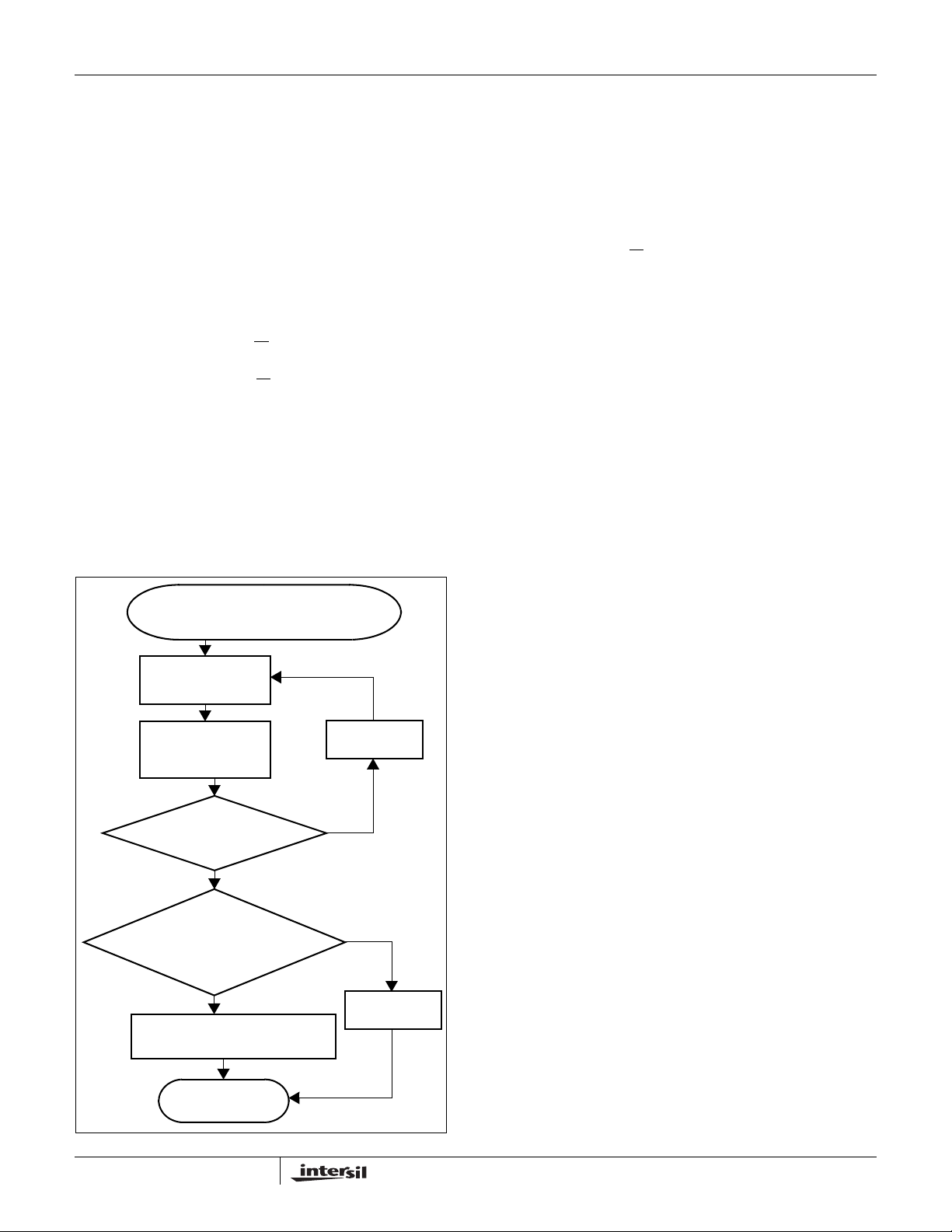
Nonvolatile Write Acknowledge Polling
After a nonvolatile write command sequence is
correctly issued (including the final STOP condition),
the X9530 initiates an internal high voltage write cycle.
Figure 14. Acknowledge Polling Sequence
Byte load completed by issuing
STOP. Enter ACK Polling
Issue START
This cycle typically requires 5 ms. During this time,
any Read or Write command is ignored by the X9530.
Write Acknowledge Polling is used to determine
whether a high voltage write cycle is completed.
During acknowledge polling, the master first issues a
START condition followed by a Slave Address Byte.
The Slave Address Byte contains the X9530’s Device
Type Identifier and Device Address. The LSB of the
Slave Address (R/W
) can be set to either 1 or 0 in this
case. If the device is busy within the high voltage
cycle, then no ACK is returned. If the high voltage
cycle is completed, an ACK is returned and the master
can then proceed with a new Read or Write operation.
(Refer to Figure 14.).
Byte Write Operation
In order to perform a Byte Write operation to the
memory array, the Write Enable Latch (WEL) bit of the
Control 6 Register must first be set to “1”. (See “WEL:
Write Enable Latch (Volatile)” on page 7.)
For any Byte Write operation, the X9530 requires the
Slave Address Byte, an Address Byte, and a Data Byte
(See Figure 15). After each of them, the X9530
responds with an ACK. The master then terminates the
transfer by generating a STOP condition. At this time, if
all data bits are volatile, the X9530 is ready for the next
read or write operation. If some bits are nonvolatile, the
X9530 begins the internal write cycle to the nonvolatile
memory. During the internal nonvolatile write cycle, the
X9530 does not respond to any requests from the
master. The SDA output is at high impedance.
Issue Slave Address
Byte (Read or Write)
ACK returned?
YES
High Voltage
complete. Continue command
sequence.
YES
Continue normal Read or Write
command sequence
PROCEED
Issue STOP
NO
NO
Issue STOP
A Byte Write operation can access bytes at locations
00h through FEh directly, when setting the Address
Byte to 00h through FEh respectively. Setting the
Address Byte to FFh accesses the byte at location
100h. The other sixteen bytes, at locations FFh and
101h through 10Fh can only be accessed using Page
Write operations. The byte at location FFh can only be
written using a “Page Write” operation.
Writing to Control bytes which are located at byte
addresses 80h through 8Fh is a special case
described in the section “Writing to Control Registers”.
16
FN8211.1
November 11, 2005
Figure 15. Byte Write Sequence
www.BDTIC.com/Intersil
Signals from
the Master
Signal at SDA
Signals from
the Slave
S
t
a
r
t
10100
Slave
Address
X9530
Write
A
C
K
Address
Byte
Data
Byte
A
C
K
S
t
o
p
A
C
K
Page Write Operation
The 2176-bit memory array is physically realized as
one contiguous array, organized as 17 pages of 16
bytes each. In order to perform a Page Write operation
to the memory array, the Write Enable Latch (WEL) bit
in Control register 6 must first be set (See “WEL: Write
Enable Latch (Volatile)” on page 7.)
A Page Write operation is initiated in the same manner
as the byte write operation; but instead of terminating
the write cycle after the first data byte is transferred,
the master can transmit up to 16 bytes (See Figure
16). After the receipt of each byte, the X9530
responds with an ACK, and the internal byte address
counter is incremented by one. The page address
remains constant. When the counter reaches the end
of the page, it “rolls over” and goes back to the first
byte of the same page.
For example, if the master writes 12 bytes to a 16-byte
page starting at location 11 (decimal), the first 5 bytes
are written to locations 11 through 15, while the last 7
bytes are written to locations 0 through 6 within that
page. Afterwards, the address counter would point to
location 7. If the master supplies more than 16 bytes of
data, then new data overwrites the previous data, one
byte at a time (See Figure 17).
The master terminates the loading of Data Bytes by
issuing a STOP condition, which initiates the
nonvolatile write cycle. As with the Byte Write
operation, all inputs are disabled until completion of
the internal write cycle.
A Page Write operation cannot be performed on the
page at locations 80h through 8Fh. Next section
describes the special cases within that page.
A Page Write operation starting with byte address
FFh, accesses the page between locations 100h and
10Fh. The first data byte of such operation is written to
location 100h.
Writing to Control Registers
The byte at location 80h, and bytes at locations 85h
through 8Fh are written using Byte Write operations.
They cannot be written using a Page Write operation.
Control bytes 1 through 4, at locations 81h through
84h respectively, are written during a single operation
(See Figure 18). The sequence must be: a START,
followed by a Slave Address byte, with the R/W
bit
equal to “0”, followed by 81h as the Address Byte, and
then followed by exactly four Data Bytes, and a STOP
condition. The first data byte is written to location 81h,
the second to 82h, the third to 83h, and the last one to
84h.
Figure 16. Page Write Operation
Write
Address
Byte
Data Byte (1)
Signals from
the Master
Signal at SDA
S
t
a
Slave
Address
r
t
10100
Signals from
the Slave
A
C
K
17
A
C
K
2 < n < 16
Data Byte (n)
A
C
K
S
t
o
p
A
C
K
FN8211.1
November 11, 2005

X9530
www.BDTIC.com/Intersil
Figure 17. Example: Writing 12 bytes to a 16-byte page starting at location 11.
7 bytes
5 bytes
5 bytes
Address=0
Address=6
The four registers Control 1 through 4, have a
nonvolatile and a volatile cell for each bit. At power-up,
the content of the nonvolatile cells is automatically
recalled and written to the volatile cells. The content of
the volatile cells controls the X9530’s functionality. If
bit NV1234 in the Control 0 register is set to “1”, a
Write operation to these registers writes to both the
volatile and nonvolatile cells. If bit NV1234 in the
Control 0 register is set to “0”, a Write operation to
these registers only writes to the volatile cells. In both
cases the newly written values effectively control the
X9530, but in the second case, those values are lost
when the part is powered down.
If bit NV1234 is set to “0”, a Byte Write operation to
Control registers 0 or 5 causes the value in the
nonvolatile cells of Control registers 1 through 4 to be
recalled into their corresponding volatile cells, as
during power-up. This doesn’t happen when the WP
pin is LOW, because Write Protection is enabled. It is
generally recommended to configure Control registers
0 and 5 before writing to Control registers 1 through 4.
Address=11
Address=7
Address Pointer
Ends Up Here
Address=15
When reading any of the control registers 1, 2, 3, or 4,
the Data Bytes are always the content of the
corresponding nonvolatile cells, even if bit NV1234 is
"0" (See “Control and Status Register Format”).
Read Operation
A Read operation consist of a three byte instruction
followed by one or more Data Bytes (See Figure 19).
The master initiates the operation issuing the following
sequence: a START, the Slave Address byte with the
bit set to “0”, an Address Byte, a second START,
R/W
and a second Slave Address byte with the R/W
to “1”. After each of the three bytes, the X9530
responds with an ACK. Then the X9530 transmits
Data Bytes as long as the master responds with an
ACK during the SCL cycle following the eigth bit of
each byte. The master terminates the read operation
(issuing a STOP condition) following the last bit of the
last Data Byte (See Figure 19).
bit set
Figure 18. Writing to Control Registers 1, 2, 3, and 4
Write
A
C
K
Address
Byte = 81h
11000
Data Byte for
Control 1
000
A
C
K
Signals from
the Master
Signal at SDA
Signals from
the Slave
S
t
a
r
t
18
Slave
Address
10100
Four Data Bytes
A
C
K
Data Byte for
Control 4
S
t
o
p
A
C
K
November 11, 2005
FN8211.1
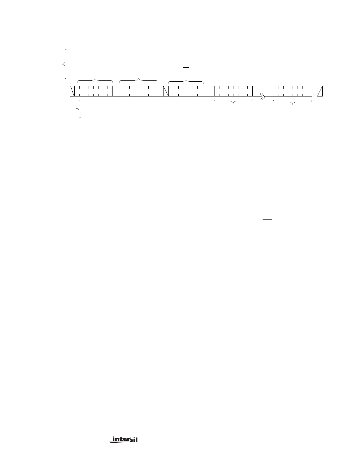
Figure 19. Read Sequence
www.BDTIC.com/Intersil
X9530
Signals
from the
Master
Signal at
SDA
Signals from
the Slave
S
t
a
r
t
Slave
Address
with
R/W
10100
= 0
Address
Byte
A
C
K
A
C
K
The Data Bytes are from the memory location indicated
by an internal pointer. This pointer initial value is
determined by the Address Byte in the Read operation
instruction, and increments by one during transmission of
each Data Byte. After reaching the memory location
10Fh the pointer “rolls over” to 00h, and the device
continues to output data for each ACK received.
A Read operation internal pointer can start at any
memory location from 00h through FEh, when the
Address Byte is 00h through FEh respectively. But it
starts at location 100h if the Address Byte is FFh.
When reading any of the control registers 1, 2, 3, or 4,
the Data Bytes are always the content of the
corresponding nonvolatile cells, even if bit NV1234 is
"0" (See “Control and Status Register Format”).
S
t
a
r
t
11100
Slave
Address
with
= 1
R/W
A
C
K
First Read
Data Byte
A
A
C
C
K
K
Last Read
Data Byte
Data Protection
There are four levels of data protection designed into
the X9530: 1- Any Write to the device first requires
setting of the WEL bit in Control 6 register; 2- The
Block Lock can prevent Writes to certain regions of
memory; 3- The Write Protection pin disables any
writing to the X9530; 4- The proper clock count, data bit
sequence, and STOP condition is required in order to
start a nonvolatile write cycle, otherwise the X9530
ignores the Write operation.
: Write Protection Pin
WP
When the Write Protection (WP
) pin is active (LOW),
any Write operations to the X9530 is disabled, except
the writing of the WEL bit.
S
t
o
p
19
FN8211.1
November 11, 2005

X9530
www.BDTIC.com/Intersil
APPLICATIONS INFORMATION
Temperature Sensing
The X9530’s on-chip temperature sensor functions
similarly to other semiconductor temperature sensors.
The surface mount package (TSSOP) and the Chip
Scale Package both allow good thermal conduction
from the PC board to the die, so the X9530 will provide
an accurate measure of the temperature of the board.
If there is no ambient air movement over the device
package or the board, then the measured temperature
will be very close to that of the board. If there is air
movement over the package and the air temperature
is substantially different from that of the PC board,
then the measured temperature will be at a value
between that of the board and the air. If the X9530 is
intended to sense the temperature of a particular
component on the board, the X9530 should be located
as close as possible to that component to minimize
contributions from other devices or the differential
temperatures across the board.
X9530 LASER DIODE BIAS APPLICATION
EXAMPLE
The X9530 is ideally suited to the control of temperature
sensitive parameters in fiber optic applications. Figure
20 shows the typical topology of a laser driver circuit
used in many fiber optic transceiver modules.
This example uses a common anode connected Laser
Diode (LD), in conjunction with a PIN Monitor PhotoDiode (MPD). The laser diode current (I
summation of the Bias Current (I
Current (I
error signal current (I
MPD current (I
) and the Automatic Power Control (APC)
MOD
MON
). The APC circuit uses the
MON
) as an input, and ensures that a
), Modulation
BIAS
) is a
LD
constant average optical power output of the LD is
maintaned. The modulation circuitry is driven by an
external high speed data source.
Typical control parameters of a LD driver circuit such
as the one shown in Figure 20 may be:
– I
MODSET
– I
BIASSET
– I
PINSET
: Sets the I
: Sets the I
: Sets the average optical power output.
MOD
BIAS
level,
level,
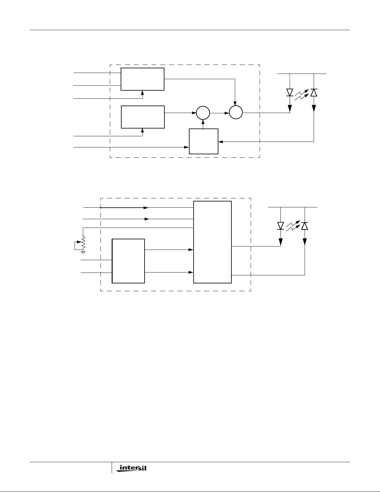
Figure 21 shows how the X9530 may be used to
control these parameters while providing accurate
temperature compensation.
In this example the I1 output of the X9530 drives the
I
MODSET
input of the laser diode circuit. By loading the
appropriate values into the look-up table (LUT1) of the
device, it can dynamically change the modulation
current of the driver circuit. This may be used to
compensate for the effect of reduced laser light output
at elevated temperatures.
Depending upon the type of driver circuit used, the I2
output of the X9530 may be used to control either
I
BIASSET
or I
21 uses I2 to control the I
I
BIASSET
is set at a fixed value using a Intersil Digital
parameters. The example in Figure
PINSET
parameter, while
PINSET
potentiometer.
Similar to the control of the modulation current, I2 may
be used to compensate for changes in I
MON
over
temperature. By loading the appropriate values into
the look-up table (LUT2) of the device, this would have
the effect of dynamically controlling the average
optical power output of the LD (via the APC circuit)
over temperature.
The lookup table values for this fiber optic application
could be determined in two ways. One way is to use
well-defined data for LD and monitor photo diode drift
over temperature, and calculate the appropriate I1 and
I2 values needed at each temperature setting. Another
way is to test the assembled module over temperature
and load values into the tables at each setting. This
will require APC on/off control to determine each
MODSET value. See Intersil application note AN156
for a full design analysis with LD driver application.
If design requirements are such that no temperature
compensation is necessary for the average optical
power output of the LD, then the I2 output pin could be
used to set the bias current. I
of the driver circuit
BIASET
may be controlled by I2 of the X9530, and the same
current level could be set with control 4 register. This
would provide a constant (temperature independant)
setting for the bias current.
As previously described, the X9530 also contains
general purpose EEPROM memory which may be
accessed by the 2 wire serial bus. In the case of
pluggable fiber optic applications such as GBIC, SFP
or SFF this memory may be used for the storage of
transceiver module parameters.
20
FN8211.1
November 11, 2005
www.BDTIC.com/Intersil
Figure 20. Typical Laser Driver Circuit Topology
X9530
Laser Diode Driver Circuit
I
BIASMAX
High Speed
Data Input
I
MODSET
I
BIASSET
I
PINSET
Modulation
Currrent
Generation
Bias
Currrent
Generation
Figure 21. X9530 Application Example Block Diagram
GBIC / SFP / XFP Module
High Speed
Data Input
I
BIASSET
SDA
SCK
X9530
I
1
I
2
I
MODSET
I
PINSET
INTERSIL
XDCP
MOD_DEF
MOD_DEF
(0)
(1)
Σ
+
–
I
APC
Automatic
Power
Control
(APC)
Laser
Diode
Driver
Circuit
I
BIAS
+
(Error Signal)
Σ
I
MOD
+
V
CC
MPDLD
I
MPDLD
I
MON
MON
I
LD
V
CC
I
LD
21
FN8211.1
November 11, 2005
X9530
www.BDTIC.com/Intersil
ABSOLUTE MAXIMUM RATINGS
All voltages are referred to Vss.
Temperature under bias ................... -65°C to +100°C
Storage temperature ........................ -65°C to +150°C
Voltage on every pin except Vcc................ -1.0V to +7V
Voltage on Vcc Pin .............................................0 to 5.5V
D.C. Output Current at pin SDA
D.C. Output Current at pins R1, R2,
VRef and VSense.................................... -0.50 to 1 mA
D.C. Output Current at pins I1 and I2 ............... -3 to 3mA
...................... 0 to 5 mA
COMMENT
Stresses above those listed under “Absolute Maximum
Ratings” may cause permanent damage to the device.
This is a stress rating only; functional operation of the
device (at these or any other conditions above those
listed in the operational sections of this specification) is
not implied. Exposure to absolute maximum rating
conditions for extended periods may affect device
reliability.
Lead temperature (soldering, 10s) .................... 300°C
OPERATING CONDITIONS
Parameter Min. Max. Units
Temperature -40 +100 °C
Temperature while writing to memory 0 +70 °C
Voltage on Vcc Pin 35.5V
Voltage on any other Pin -0.3 Vcc + 0.3 V
ELECTRICAL CHARACTERISTICS
All typical values are for 25°C ambient temperature and 5 V at pin Vcc. Maximum and minimum specifications are
over the recommended operating conditions. All voltages are referred to the voltage at pin Vss unless otherwise
specified. All bits in control registers are “0” unless otherwise specified. 510Ω, 0.1%, resistor connected between R1
and Vss, and another between R2 and Vss unless otherwise specified. 400kHz TTL input at SCL unless otherwise
specified. SDA pulled to Vcc through an external 2kΩ resistor unless otherwise specified. 2-wire interface in “standby”
(see notes 1 and 2 on page 22), unless otherwise specified. WP
, A0, A1, and A2 floating unless otherwise specified.
VRef pin unloaded, unless otherwise specified.
Symbol Parameter Min Typ Max Unit Test Conditions / Notes
Iccstby Standby current into Vcc
pin
Iccfull Full operation current into
Vcc pin
Iccwrite Nonvolatile Write current
into Vcc pin
I
PLDN
V
ILTTL
V
IHTTL
I
INTTL
V
OLSDA
I
OHSDA
V
ILCMOS
On-chip pull down
current at WP
A2
SCL and SDA, input Low
voltage
SCL and SDA, input High
voltage
SCL and SDA input
current
SDA output Low voltage 0 0.4 V I(SDA) = 2 mA
SDA output High current 0 100 μA V(SDA) = Vcc
WP, A0, A1, and A2 input
Low voltage
, A0, A1,and
4 mA Average from START condition until
0120μAV(WP
2.0 V
-1 10 μA Pin voltage between 0 and Vcc, and
0 0.2 x
2 mA R1 and R2 floating, VRef unloaded.
9 mA 2-wire interface reading from
and I2 both connected to
1
), V(A0), V(A1), and V(A2) from
0.8 V
Vcc
memory, I
Vss, DAC input bytes: FFh, VRef
unloaded.
after the STOP condition
t
WP
WP
: Vcc, R1 and R2 floating,
VRef unloaded.
0V to Vcc
SDA as an input.
V
22
FN8211.1
November 11, 2005
X9530
www.BDTIC.com/Intersil
ELECTRICAL CHARACTERISTICS (CONTINUED)
All typical values are for 25°C ambient temperature and 5 V at pin Vcc. Maximum and minimum specifications are
over the recommended operating conditions. All voltages are referred to the voltage at pin Vss unless otherwise
specified. All bits in control registers are “0” unless otherwise specified. 510Ω, 0.1%, resistor connected between R1
and Vss, and another between R2 and Vss unless otherwise specified. 400kHz TTL input at SCL unless otherwise
specified. SDA pulled to Vcc through an external 2kΩ resistor unless otherwise specified. 2-wire interface in “standby”
(see notes 1 and 2 on page 22), unless otherwise specified. WP
VRef pin unloaded, unless otherwise specified.
Symbol Parameter Min Typ Max Unit Test Conditions / Notes
V
IHCMOS
VRefout Output Voltage at VRef at
WP, A0, A1, and A2 input
High voltage
0.8 x
Vcc
1.205 1.21 1.215 V -20 μA ≤ I(VRef) ≤ 20 μA
25°C
RVref VRef pin input resistance 20 40 kΩ VRM bit = “1”, 25°C
TCOref Temperature coefficient of
-100 +100 ppm/°CSee note 4 and 5.
VRef output voltage
VRef Range Voltage range when VRef
1 1.3 V See note 3.
is an input
TSenseRange Temperature sensor
-40 100 °C See note 4.
range
I
R
Current from pin R1 or R2
0 1600 μA
to Vss
V
POR
Power-on reset threshold
1.5 2.8 V
voltage
VccRamp Vcc Ramp Rate 0.2 50 mV /
V
ADCOK
ADC enable minimum
2.6 2.8 V See Figure 8.
voltage
, A0, A1, and A2 floating unless otherwise specified.
Vcc V
s
μ
Notes: 1. The device goes into Standby: 200 ns after any STOP, except those that initiate a nonvolatile write cycle. It goes into Standby tWC after
a STOP that initiates a nonvolatile write cycle. It also goes into Standby 9 clock cycles after any START that is not followed by the correct Slave Address Byte.
is the time from a valid STOP condition at the end of a write sequence to the end of the self-timed internal nonvolatile write cycle. It
2. t
WC
is the minimum cycle time to be allowed for any nonvolatile write by the user, unless Acknowledge Polling is used.
3. For this range of V(VRef) the full scale sink mode current at I1 and I2 follows V(VRef) with a linearity error smaller than 1%.
4. These parameters are periodically sampled and not 100% tested.
5. TCO
= [Max V(V
ref
) - Min V(V
REF
)] x 106/(1.21V x 140°C)
REF
23
FN8211.1
November 11, 2005

X9530
www.BDTIC.com/Intersil
D/A CONVERTER CHARACTERISTICS
All typical values are for 25°C ambient temperature and 5 V at pin Vcc. Maximum and minimum specifications are over the
recommended operating conditions. All voltages are referred to the voltage at pin Vss unless otherwise specified. All bits in
control registers are “0” unless otherwise specified. 510Ω, 0.1%, resistor connected between R1 and Vss, and another
between R2 and Vss unless otherwise specified. 400kHz TTL input at SCL unless otherwise specified. SDA pulled to Vcc
through an external 2kΩ resistor unless otherwise specified. 2-wire interface in “standby” (see notes 1 and 2 on page 22),
unless otherwise specified. WP
Symbol Parameter Min Typ Max Unit Test Conditions / Notes
IFS
00
I1 or I2 full scale current, with external
resistor setting
IFS
01
I1 or I2 full scale current, with internal
low current setting option
IFS
10
I1 or I2 full scale current, with internal
middle current setting option
IFS
11
I1 or I2 full scale current, with internal
high current setting option
Offset
DAC
FSError
DNL
DAC
DAC
I1 or I2 D/A converter offset error 1 1 LSB
I1 or I2 D/A converter full scale error -2 2 LSB
I1 or I2 D/A converter
Differential Nonlinearity
INL
DAC
I1 or I2 D/A converter Integral Nonlinearity with respect to a straight line
through 0 and the full scale value
VISink I1 or I2 Sink Voltage Compliance 1.2 Vcc V In this range the current at I1
VISource I1 or I2 Source Voltage Compliance 0 Vcc-1.2 V In this range the current at I1
I
OVER
I1 or I2 overshoot on D/A Converter
data byte transition
I
UNDER
I1 or I2 undershoot on D/A Converter
data byte transition
t
rDAC
I1 or I2 rise time on D/A Converter data
byte transition; 10% to 90%
TCO
I1I2
Temperataure coefficient of output
current I1 or I2 when using internal
resistor setting
Notes: 1. LSB is defined as divided by the resistance between R1 or R2 to Vss.
2. Offset
expressed in LSB.
FSError
is expressed in LSB. The Offset
DNL
the output of the DAC, when the input changes by one code step. It is expressed in LSB. The measured values are adjusted for Offset
and Full Scale Error before calculating DNL
INL
ing the measured transfer curve for Offset and Full Scale Error. It is expressed in LSB.
3. These parameters are periodically sampled and not 100% tested.
: The Offset of a DAC is defined as the deviation between the measured and ideal output, when the DAC input is 01h. It is
DAC
: The Full Scale Error of a DAC is defined as the deviation between the measured and ideal output, when the input is FFh. It
DAC
: The Differential Non-Linearity of a DAC is defined as the deviation between the measured and ideal incremental change in
DAC
: The Integral Non-Linearity of a DAC is defined as the deviation between the measured and ideal transfer curves, after adjust-
DAC
, A0, A1, and A2 floating unless otherwise specified.
1.56 1.58 1.6 mA DAC input Byte = FFh,
0.3 0.4 0.5 mA
0.64 0.85 1.06 mA
11.3 1.6mA
-0.5 0.5 LSB
-1 1 LSB
530μs
±200
23V(VRef)
x
[]
255
is subtracted from the measured value before calculating FSError
DAC
.
DAC
Source or sink mode, V(I1)
and V(I2) are Vcc - 1.2V in
source mode and 1.2V in sink
mode.
See notes 1 and 2.
or I2 vary < 1%
or I2 vary < 1%
0 μA DAC input byte changing from
00h to FFh and vice
0 μA
versa, V(I1) and V(I2) are
Vcc - 1.2V in source mode
and 1.2V in sink mode.
See note 3.
ppm/°CSee Figure 5.
Bits I1FSO[1:0] ¦ 00
2
or
Bits I2FSO[1:0] ¦ 002,
VRMbit = “1”
.
DAC
24
FN8211.1
November 11, 2005
X9530
www.BDTIC.com/Intersil
A/D CONVERTER CHARACTERISTICS
All typical values are for 25°C ambient temperature and 5 V at pin Vcc. Maximum and minimum specifications are over the
recommended operating conditions. All voltages are referred to the voltage at pin Vss unless otherwise specified. All bits in control
registers are “0” unless otherwise specified.
unless otherwise specified. 400kHz TTL input at SCL unless otherwise specified. SDA pulled to Vcc through an external 2kΩ resistor
unless otherwise specified. 2-wire interface in “standby” (see notes 1 and 2 on page 22), unless otherwise specified. WP
floating unless otherwise specified.
Symbol Parameter Min Typ Max Unit Test Conditions / Notes
ADCTIME A/D converter conversion
time
RIN
ADC
VSense pin input
resistance
CIN
ADC
VSense pin input
capacitance
VIN
ADC
Offset
ADC
FSError
ADC
VSense input signal range 0 V(VRef) V This is the A/D Converter
A/D converter offset error -0.25 0.25 LSB See notes 1 and 2
A/D converter full scale error
DNL
ADC
A/D Converter Differential
Nonlinearity
INL
ADC
A/D converter Integral
Nonlinearity
TempStep
ADC
Temperature step causing
one step increment of ADC
output
Out25
ADC
ADC output at 25°C 011101
510Ω, 0.1%, resistor connected between R1 and Vss, and another between R2 and Vss
, A0, A1, and A2
9 ms Proportional to A/D converter
input voltage. This value is
maximum at full scale input
of A/D converter.
ADCfiltOff = “1”
100 kΩ VSense as an input,
ADCIN bit = “1”
1 7 pF VSense as an input,
ADCIN bit = “1”,
Frequency = 1 MHz
See note 3.
Dynamic Range. ADCIN bit = “1”
-1 1 LSB
-0.5 0.5 LSB
-0.5 0.5 LSB
2.1 2.2 2.3 °C
2
Notes: 1. “LSB” is defined as V(VRef)/63, “Full Scale” is defined as V(VRef).
2. Offset
amount of deviation between the measured first transition point and the ideal point.
FSError
of deviation between the measured last transition point and the ideal point,
after subtracting the Offset from the measured curve.
DNL
expressed in LSBs. The measured transfer curve is adjusted for Offset and Fullscale errors before calculating DNL.
INL
defined as the sum of the DNL errors starting from code 00h to the code where the INL measurement is desired. The measured transfer curve is adjusted for Offset and Fullscale errors before calculating INL.
3. These parameters are periodically sampled and not 100% tested.
: For an ideal converter, the first transition of its transfer curve occurs a above zero. Offset error is the
ADC
: For an ideal converter, the last transition of its transfer curve occurs at .Full Scale Error is the amount
ADC
: DNL is defined as the difference between the ideal and the measured code transitions for successive A/D code outputs
ADC
: The deviation of the measured transfer function of an A/D converter from the ideal transfer function. The INL error is also
ADC
25
31/2 x V(VRef)
[]
255
2511/2 x V(VRef)
[]
255
FN8211.1
November 11, 2005

X9530
www.BDTIC.com/Intersil
2-WIRE INTERFACE A.C. CHARACTERISTICS
Symbol Parameter Min Typ Max Units Test Conditions / Notes
f
SCL
(4)
t
IN
(4)
t
AA
(4)
t
BUF
t
LOW
t
HIGH
t
SU:STA
t
HD:STA
t
SU:DAT
t
HD:DAT
t
SU:STO
t
DH
(4)
t
R
(4)
t
F
t
SU:WP
t
HD:WP
(4)
Cb
(4)
(4)
SCL Clock Frequency 1
Pulse width Suppression Time at
inputs
SCL Low to SDA Data Out Valid 900 ns
Time the bus free before start of new
transmission
Clock Low Time 1.3 1200
Clock High Time 0.6 1200
Start Condition Setup Time 600 ns
Start Condition Hold Time 600 ns
Data In Setup Time 100 ns
Data In Hold Time 0 μs
Stop Condition Setup Time 600 ns
Data Output Hold Time 50 ns
SDA and SCL Rise Time 20
SDA and SCL Fall Time 20
WP Setup Time 600 ns
WP Hold Time 600 ns
Capacitive load for each bus line 400 pF
(3)
400 kHz See “2-Wire Interface Test
50 ns
1300 ns
(3)
(3)
300 ns
300 ns
+0.1Cb
+0.1Cb
(1)
(1)
Conditions” (below),
See Figure 22, Figure 23
and Figure 24.
μs
μs
2-WIRE INTERFACE TEST CONDITIONS
Input Pulse Levels 10 % to 90 % of Vcc
Input Rise and Fall Times, between 10% and 90% 10 ns
Input and Output Timing Threshold Level 1.4V
External Load at pin SDA 2.3 k
Ω to Vcc and 100 pF to Vss
NONVOLATILE WRITE CYCLE TIMING
Symbol Parameter Min Typ Max Units Test Conditions / Notes
(2)
t
WC
Notes: 1. Cb = total capacitance of one bus line (SDA or SCL) in pF.
Nonvolatile Write Cycle Time 5 10 ms See Figure 24
2. t
is the time from a valid STOP condition at the end of a write sequence to the end of the self-timed internal nonvolatile write cycle. It
WC
is the minimum cycle time to be allowed for any nonvolatile write by the user, unless Acknowledge Polling is used.
3. The minimum frequency requirement applies between a START and a STOP condition.
4. These parameters are periodically sampled and not 100% tested.
26
FN8211.1
November 11, 2005

TIMING DIAGRAMS
www.BDTIC.com/Intersil
Figure 22. Bus Timing
X9530
SCL
t
SU:STA
SDA IN
SDA OUT
Figure 23. WP
SDA IN
t
HD:STA
Pin Timing
SCL
WP
t
F
START
t
SU:DAT
t
SU:WP
t
HIGH
Clk 1
t
LOW
t
HD:DAT
t
R
t
HD:WP
t
SU:STO
t
t
DH
AA
STOP
t
BUF
Figure 24. Non-Volatile Write Cycle Timing
SCL
SDA
8th bit of last byte
ACK
Stop
Condition
t
WC
Start Condition
27
FN8211.1
November 11, 2005

X9530
www.BDTIC.com/Intersil
14-Lead Plastic, TSSOP, Package Code V14
.025 (.65) BSC
0° - 8°
.0075 (.19)
.0118 (.30)
.193 (4.9)
.200 (5.1)
.019 (.50)
.029 (.75)
Detail A (20X)
.169 (4.3)
.177 (4.5)
.041 (1.05)
.002 (.05)
.006 (.15)
.010 (.25)
Gage Plane
Seating Plane
.252 (6.4) BSC
.031 (.80)
.041 (1.05)
See Detail “A”
NOTE: ALL DIMENSIONS IN INCHES (IN PARENTHESES IN MILLIMETERS)
All Intersil U.S. products are manufactured, assembled and tested utilizing ISO9000 quality systems.
Intersil Corporation’s quality certifications can be viewed at www.intersil.com/design/quality
Intersil products are sold by description only. Intersil Corporation reserves the right to make changes in circuit design, software and/or specifications at any time without
notice. Accordingly, the reader is cautioned to verify that data sheets are current before placing orders. Information furnished by Intersil is believed to be accurate and
reliable. However, no responsibility is assumed by Intersil or its subsidiaries for its use; nor for any infringements of patents or other rights of third parties which may result
from its use. No license is granted by implic atio n or other wise u nde r any p a tent or patent rights of Intersil or it s subs idi aries.
For information regarding Intersil Corporation and its products, see www.intersil.com
28
FN8211.1
November 11, 2005
 Loading...