

Page 1
TM
Memory Power System Solution
ISL6225 Dual PWM Controller Provides Complete DDR
Application Note December 2001
Introduction
As computer memory bandwidth is pushed further and
further to multi-Gb/s levels, new memory technologies are
emerging. The DDR (Dual Data Rate) memory is an
evolutionary step on this path that along with increased data
rate maintains the low cost legacy of SDRAMs and thus will
dominate most PC markets for several years to come [1].
The DDR memory not only increases the memory bandwidth
but also reduces memory power consumption. The major
contributors to reduced power consumption are lower
operating voltage, lower signal voltage swing associated with
SSTL_2 logic, and reduced time spent in an active mode. All
these features make DDR memory a desirable component
for mobile, battery-powered applications [2, 3].
DDR Memory Power Requirements
The new memory comes with some additional requirements.
The increased bandwidth made available by SSTL_2
signaling require special clock techniques, proper layout, a
power source tracking reference signal, and line termination.
AN9995
Author: Vladimir A. Muratov, Steven P. Laur
memory operates with a double rate. Practically, the VTT
current gets dramatically averaged in output capacitors due
to a low duty factor (~15 to 30%) of read-write states [4]. The
terminating VTT power supply requirements depend only on
the number of lines and value of the terminating resistors
used and does not vary with memory size. Measurements
done in practical circuits show typical current levels in a
range of 0.5A. Tests show that the more memory is engaged
by the software, the lower is VTT current. All these suggests
that the same optimized solution can be used for various
computer applications.
The VDDQ power supply usually provides current not only to
the memory banks, but to a ‘north bridge’ controller and
some other circuitry as well. The current has a permanent
base level in a range of 2.0–3.0A. The base level depends
on how aggressive the power management scheme of a
memory controller isand also varies with memory size. The
bigger memory draws more current on background.
Depending on the computing task performed, the current
can peak up to 4.0A.
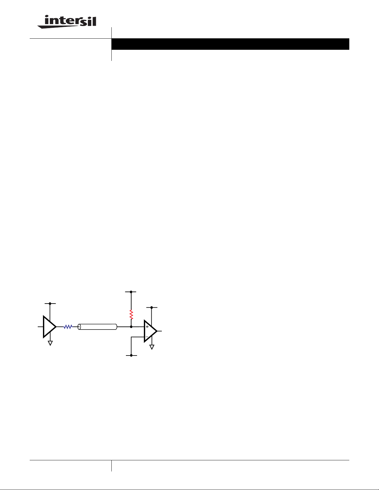
The important part of SSTL_2 signaling is that bus signals
are referenced to the reference voltage VREF that is usually
held symmetrically between VDDQ and VSS. It is important
that VREF stays symmetrically positioned between VDDQ
and VSS levels over variations in environmental and supply
parameters, Figure 1. The termination voltage VTT should
be within ±40mV of VREF. The VDDQ voltage, currently 2.5V
nominal value, should have ±200mV tolerance.
VTT=VDDQ/2
VDDQ
Transmitter
=50Ω
R
TT
RS=22Ω
FIGURE 1. DDR MEMORY TERMINATION
Line
50Ω
VREF=VDDQ/2
VDDQ
Receiver
Each terminated line consumes 16.2 mA. With about 125
lines compliant with SSTL_2 specifications, this theoretically
makes maximum current capability of VTT supply
Imax=2.025A, sourcing or sinking. In reality, the front bus is
operating on frequency of 100MHz, 133MHz and any given
memory state is actively present on the bus for a very short
moment of time of several tens of nanoseconds as DDR
ISL6225–Provides Complete Power
Solution for DDR Memory
The ISL6225 dual switcher accomplishes all of the goals
associated with DDR memory power by combining two
synchronous PWM voltage regulators into a single IC. Its
unique design allows the IC to both source and sink current
on one of the channels. This ability allows the IC to be
adapted very effectively to a DDR memory power solution
when the DDR pin is set high.
The first PWM channel is used to regulate 2.5VDC (V
a typical “buck” regulator fashion. The output voltage of the
first channel is set to the required VDDQ level by the external
voltage divider. This makes the chip compatible not only with
current DDR memory specifications, but, also, with future
DDR II requirements. To provide the required tracking
function, the output of this regulated voltage is divided down
to 1.25VDC by an external R/R divider and fed back into the
IC as a tracking reference voltage.The reference voltage
VREF required by the DDR memory chips is provided via the
PG2/REF pin that can source up to 10mA. This output also
serves as a reference for the VTT channel. The second
channel will then regulate to 1.25VDC (V
) with high
TT
precision.
Please refer to the ISL6225 datasheet, FN9049, for more
information [5].
DDQ
)in
1
CAUTION: These devices are sensitive to electrostatic discharge; follow proper IC Handling Procedures.
1-888-INTERSIL or 321-724-7143
|
Intersil (and design) is a trademark of Intersil Americas Inc.
Copyright © Intersil Americas Inc. 2001. All Rights Reserved
Page 2
JP2
FCCM
JP5
VINPRG
Jumper View
Application Note AN9995
Quick Start Evaluation
Out Of The Box
The ISL6225EVAL1 comes in a “ready-to-test” state. The
board comes equipped with several jumpers pre-populated
for battery operation. Use Table 1, which describes jumper
function, for test setup. Table 2 illustrates the input and
output voltage and current specifications.
NOTE: Note: This Application Note is for the DDR solution only.
Required Test Equipment
To fully test the ISL6225 chip functionality characterized by
this Application Note, the follow equipment is needed:
•4 channel oscilloscope with probes
•2 electronic loads
•2 bench power supplies
• precision digital multi-meters
• Digital pulse generator
TABLE 1. JUMPER FUNCTIONALITY
Jumper # State Function
JP1 POP Normal Operation
NOP Measure operating current I
JP2 POS1 Enable hysteretic operation
POS2 FCCM mode
JP3 POP Connect EN1 to VCC
NOP External EN1
JP4 POP Connect EN2 to VCC
NOP External EN2
JP5 POS1 Operate in Battery Mode
POS2 Operate in 5V Mode
Power Connections
With the all supplies turned OFF, connect the 0-24V power
supply positive terminal to the VIN post (J2) on the EVAL
board and the negative terminal to the nearest GND post
(J3). Then connect the 0-5V power supply positive terminal
to the VCC post (J4) and the negative terminal to the nearest
GND post (J1)
It should be noted that VIN must be powered up prior to VCC
in all cases.
.
TABLE 2. INPUT/OUTPUT VOLTAGE/CURRENT
OPERATING SPECIFICATIONS.
VIN VCC VDDQ VTT
Voltage
Imax
Inom
5-24V 5V 2.5V 1.25V
3A 3A 6A 3A
--3A2A
VCC
Load Connections
Connect the first electronic load positive terminal to VDDQ
(J5) and the negative terminal to GND (J6). Connect the
positive terminal of the second electronic load to VTT (J6)
and negative terminal to the nearest GND post (J9).
Performance Characterization
This section will show measured performance data from a
standard bench setup. It will include descriptions of each
experiment performed and how to recreate them.
NOTES:
•Jumper JP1 should be populated.
•Connect JP2 in FCCM mode
•Connect JP5 in the EN5V position.
•VIN = 5V, VCC = 5V.
Modes of Operation
Figure 10 shows a typical circuit for One-Step Conversion.
This is accomplished by populating jumper JP5 in POS1. In
this arrangement, V
battery voltage. V
V
output. This setup has the advantage of not requiring
DDQ
a regulated system voltage to supply the power train.
Tw o-Step Conversion is also available on the ISL6225 DDR
evaluation board. This approach requires a regulated 5 volt
system rail to provide power to the converters. The V
converter takes the system rail voltage while the V
converter is cascaded from V
tied to GND through a 100kOhm resistor. This is done by
populating jumper JP5 in POS2 and tying the V
terminals together on the application board.
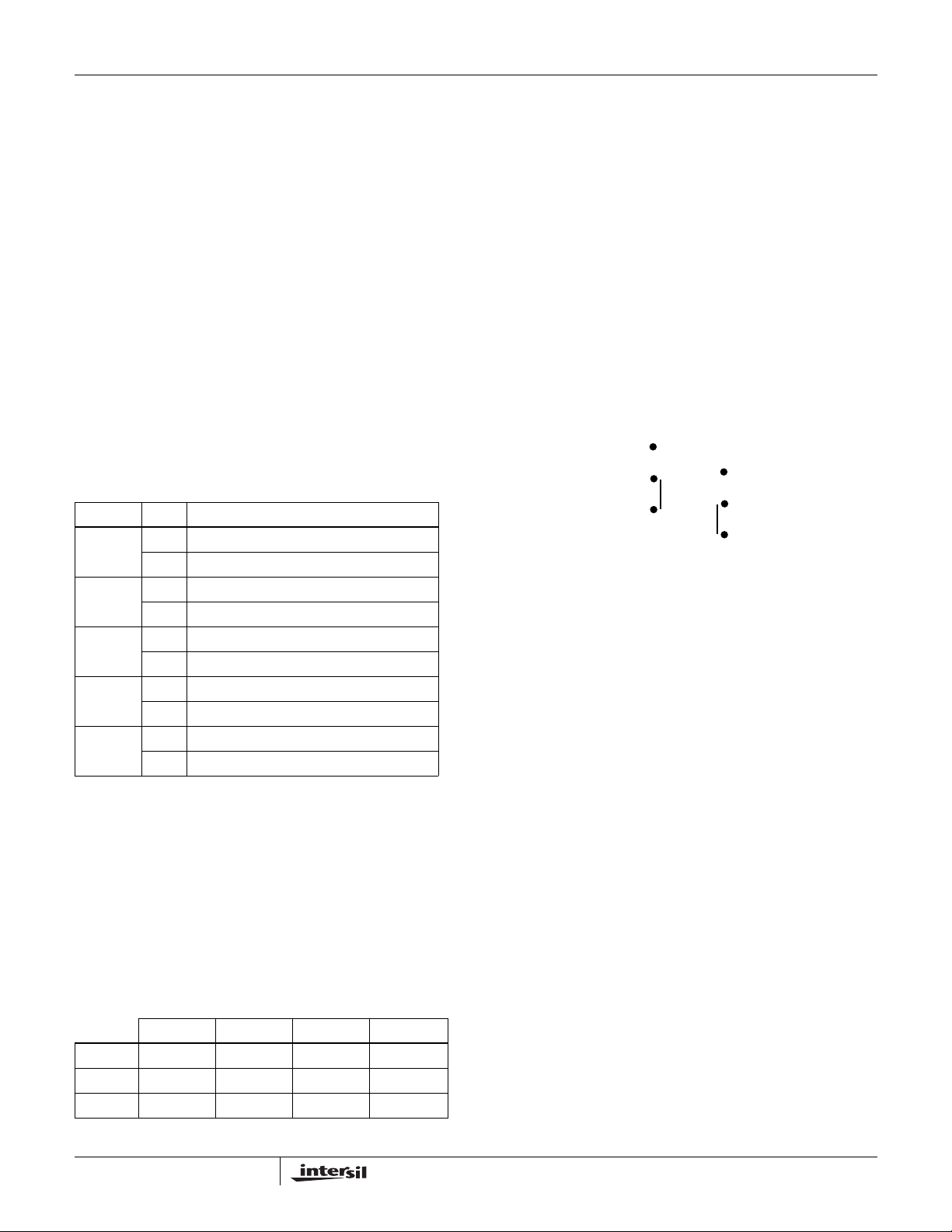
Soft-Start
In a start up event, the IC is required to ramp both output
voltages smoothly to their programmed level. To do this, the
chip must disable the undervoltage and pgood circuitry until
the output has risen to within 75% of its target. Only then is
PGOOD released and the part allowed to operate normally.
With I
Figure 2.
• Connect the digital pulse generator to JP3 and JP4 to
allow for external enabling of the chip.
• Set the scope to trigger on EN (J12).
VDDQ
= I
VTT
is converted directly from the
DDQ
is then converted directly from the
TT
DDQ
CC
TT
IN
and V
must be
. In this case, V
DDQ
= 3A, the start up event is captured in
IN
2
Page 3
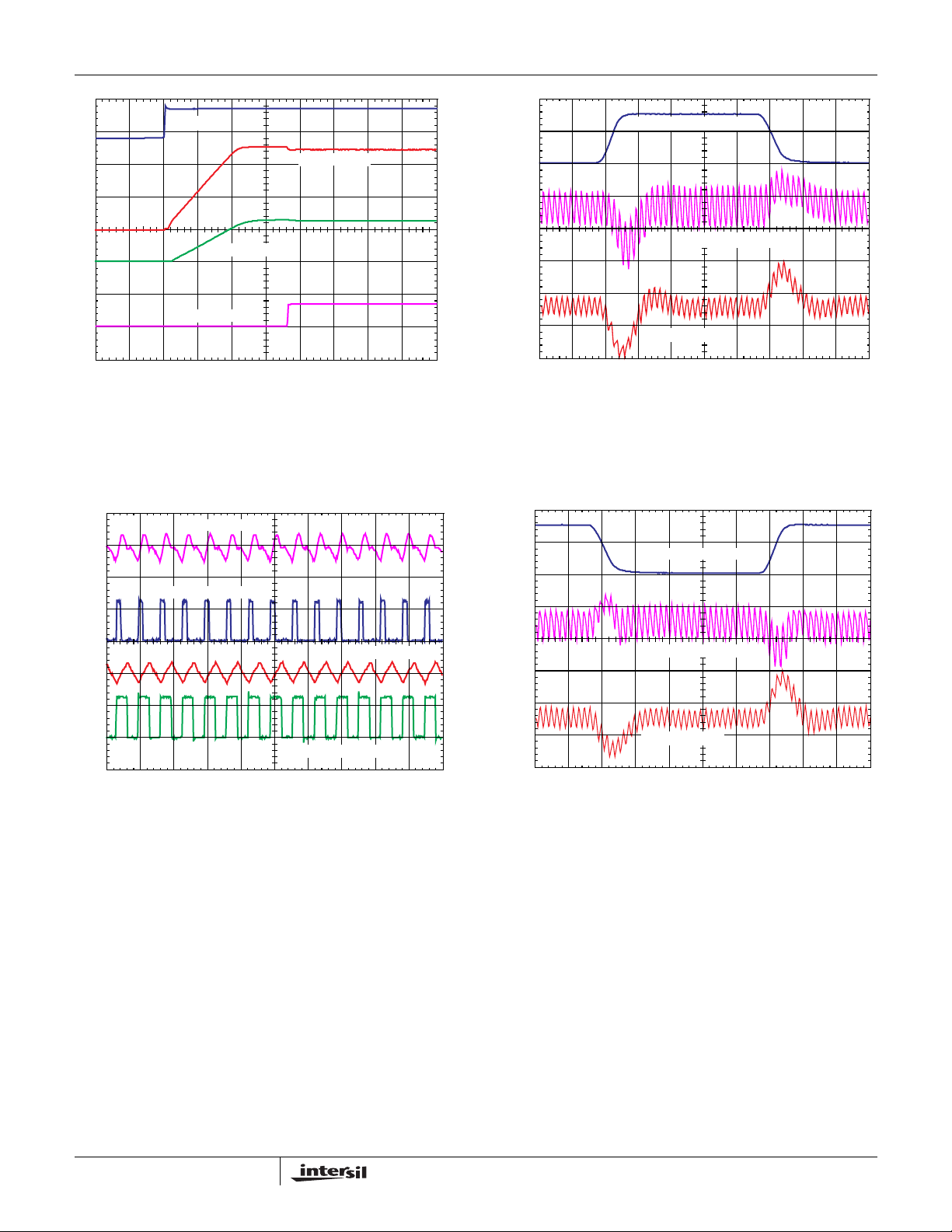
FIGURE 4. LOAD TRANSIENT (VTT - GND)
VDDQ, 50mV/div
VTT, 50mV/div
20us / div
0A
2.5V
1.25V
Load Current, 2A/div
FIGURE 5. LOAD TRANSIENT (VDDQ - VTT)
VTT, 50mV/div
VDDQ, 50mV/div
Load Current, 2A/div
20us/div
1.25V
2.5V
0A
Application Note AN9995
0V
0V
0V
0V
EN, 5V/div
VDDQ, 1V/div
VTT, 1V/div
PGOOD, 5V/div
1ms/div
FIGURE 2. INITIAL START UP
Steady-State Operation
Under normal operating conditions, the ISL6225 should
regulate 2.5V and 1.25V with minimal effort and output
voltage ripple. Figure 3 illustrates converter waveforms
during normal operating conditions.
VDDQ, 50mV/div
2.5V
Sinking Mode (V
DDQ
to V
TT
)
The output voltage excursion under a load transient in
sinking mode is shown in Figure 5. The load swings 0-3A
from V
between V
DDQ
into V
DDQ
. Reconfigure the second electronic load
TT
and V
for this experiment.
TT
PHASE_VDDQ, 10V/div
0V
1.25V
0V
PHASE_VTT, 2V/div
5us/div
FIGURE 3. NORMAL OPERATION
VTT, 50mV/div
Transient Response
The ISL6225 in DDR applications is required to handle load
transients of 0-3A on V
load of 3A from V
DDQ
Sourcing Mode (V
The output voltage excursion under a load transient event is
shown in Figure 4. The load swings 0-3A from V
. For these tests, there is a static
TT
to GND.
to GND)
TT
TT
.
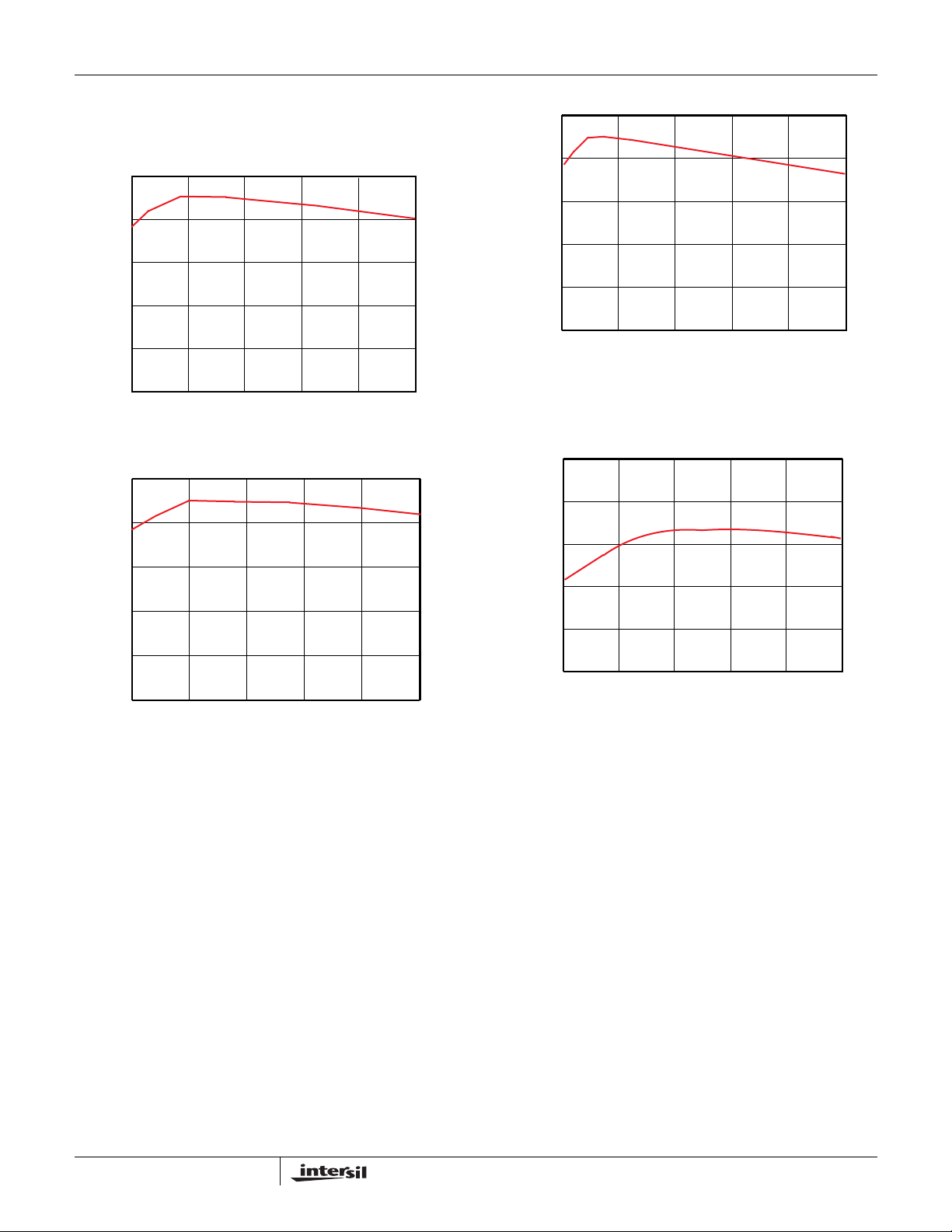
Efficiency
It is important to illustrate that each channel of the ISL6225
is highly efficient, which contributes to an overall high system
efficiency. Figures 6...9 demonstrate all perspectives of
efficiency for the ISL6225 in DDR mode.
NOTE:
•Measure voltage at board terminals
•Allow thermal equilibrium
•TA = 25C
•No forced air
3
Page 4
4
FIGURE 8. VDDQ EFFICIENCY
Output Current (A)
0.8
1.35
1.9
2.45
3.0
0.25
70
75
80
85
90
95
Efficiency (%)
FIGURE 9. OVERALL EFFICIENCY
Output Current (A)
0.8
1.1
1.4
1.7
2
0.5
70
75
80
85
90
95
Efficiency (%)
Application Note AN9995
Individual channel efficiency for V
is captured for both
TT
sinking and sourcing current in Figure 6 and Figure 7
respectively.
95
90
85
80
Efficiency (%)
75
70
0.25
0.6
Output Current (A)
0.95
FIGURE 6. VTT EFFICIENCY. SOURCING MODE
95
90
1.3
1.65
2
Overall efficiency for the ISL6225 in DDR mode can be seen
in Figure 9.
85
80
Efficiency (%)
75
70
0.25
0.6
Output Current (A)
FIGURE 7. VTT EFFICIENCY. SINKING MODE
The individual channel efficiency for V
Figure 8. Both V
TT
and V
90% for nearly all loading conditions.
0.95
1.3
DDQ
provide efficiency greater than
DDQ
1.65
is illustrated in
2
References
1. JEDEC STANDARD JESD8-9A. Stub Series Terminated
Logic for 2.5V (SSTL_2)
2. L.L. Wang, P. Leung, F. Tabrizi, ‘DDR DRAMs Pare Down
Power for Laptops’, Portable Design, July 2000
3. V. Muratov, S. Wiktor, J. Li, ‘Powering DDR Memory --
Mysteries and Realities’, PCIM -- HFPC 2001, pp. 11-18
4. J. Janzen, ‘Calculating Memory System Power for DDR
SDRAM,’ Micron Application Note, 2001
5. ISL6225 Data Sheet, Intersil Corporation, File No.
FN9049
Intersil documents are available on the web at
http://www.intersil.com.
Page 5

ISL6225 EVAL1 Schematic
The evaluation board schematic is shown in Figure 10. The board allows evaluation of ISL6225 performance for DDR memory using either single-step or dual-step power
conversion schemes. The recommended Bill of Materials (BOM) is presented in Table 3.
5V
1 2
12
C4
+
68u (OPT)
16V
TP2
Probe Socket
C8
1.0uF
10V1
2
L1
4.7u
Sumida CDRH124-4R7MC
1
C11
1
15n
50V
12
C13
2
NOP
+
2
4V
1
2
12
+
5
JP1
R8
17k8
R10
10k0
VOUT1
C24
NOP
4V
C2
1
C3
1
10u
10u
25V
25V
2
2
D1
BAT54WT1
13
2
R2 0R
2
1
U2
C9
1
0.15
2
1
3
1
2
J11
16V
TP4
FCCM
JP2
2
C25
4.7
10V
1
1
1
R7
NOP
2
C17
1
1n
50V
2
2
RED GREEN
PG1
6
7
8
IRF7813
IRF7313
5V
2
R15
680R
1
1
13
24
32
1
1
R16
680R
CR1
LXA3025IGC-TR
Q1
BSS123LT1
J1
1
GND
5
D D
VCC
J4
1
C C
VDDQ
J5
1
VOUT1
12
C12
+
220u
4V
B B
J7
1
GND
A A
PGOOD
5
4
1
VIN
2
JP5
3
U1
1
GND
2
LGATE1
3
45
3
R4 1k00
2
1
1
C18
1
NOP
2
10V
1
R9
49.9k
2
C20
0.01
1
10V
2
PGND1
4
PHASE1
5
UGATE1
6
BOOT1
2
7
ISEN1
8
EN1
9
VOUT1
10
VSEN1
11
OCSET1
12
SOFT1
13
DDR
14 15
VIN PG1
ISL6225
VCC
5V
EN1 EN2
JP4
JP3
1 2
1 2
1
1
R17
R18
680R
680R
2
2
1
J12
4
1
1
R20
R19
10k
10k
2
2
3
1
R1
100k
2
VCC
C5
4.7
1
10V
2
28
VCC
27
LGATE2
26
PGND2
25
PHASE2
24
UGATE2
23
BOOT2
ISEN2
VOUT2
VSEN2
OCSET2
SOFT2
PG2/REF
J8
V_REF
J10
1
2
22
21
EN2
20
19
18
17
16
PG1VIN
1
1
C21
NOP
10V
1
1
C23
2
4.7
10V
2
C22
1
2
NOP
10V
GND
1
EN2EN1
J13
3
1
GND
J14
2
VOUT1
2
1
U3
4 5
3
2
1
IRF7813
IRF7313
VOUT1
1
R11
10k0
2
1
C26
1
R14
1u
10k0
10V
2
2
2
1
1
12
+
C1
NOP
25V
1
D2
C6
1
4.7
10V
2
6
7
8
Title
Size Document Number Rev
Date:
13
BAT54WT1
2
C7
TP1
1.0
Probe SocketR3 0R
10V
1
2
C10
1
0.15
16V
L2
TP3
1.5u
2
Panasonic ELL6SH4R7MR5 5k90
1
1
R6
NOP
2
C19
1
1n
50V
2
1
2
R12
NOP
12
C14
220u
+
4V
1
R13
NOP
2
INTERSIL
ISL6225 EVALUATION BOARD (DDR)
B
ISL6225eval_DDR
11Tuesday, September 25, 2001
Sheet of
1
1
12
+
1
Building 2A,Suite 105
4020 Stirrup Creek Drive
Durham, NC 27703
Phone: (919) 405 3650
Fax: (919) 405 3651
J2
J3
VTT
J6
C15
NOP
4V
J9
GND
Vin
GND
1
2
Application Note AN9995
C16
4.7
10V
A
FIGURE 10. APPLICATION BOARD SCHEMATIC
Page 6

Application Note AN9995
Bill of Materials
TABLE 3. BILL OF MATERIALS
Qty Reference Description Package Vendor Part No.
1 CR1 LED LXA3025IGC-TR
1C1 NOP Sanyo OSCON 25SP56M
2 C2, C3 10uF Tayo Yuden TMK432BJ106KM
1C4 68uF (OPT) KEMET T494D686(1)016AS
5 C5, C6, C16, C23, C25 4.7uF Tayo Yuden LMK316BJ475ML
3 C18, C21, C22 NOP KEMET C1206C105K8RAC
2 C7, C8 1.0uF KEMET C1206C105K8RAC
2 C10, C9 150nF KEMET C0805C154K4RAC
1 C11 15nF KEMET C0805C102K5RAC
2 C17, C19 1.0nF KEMET C0805C102K5RAC
2 C12, C14 220uF Sanyo 4TPB220ML
1 C20 0.01uF KEMET C0805C103K4RAC
1 C26 10nF KEMET C0805C103K4RAC
3 C13, C15, C24 NOP Sanyo TPB330ML
2 D1, D2 Diode Motorola BAT54WT1
3 JP1, JP3, JP4 2-Terminal Jumper Berg header# 68000-236
shunt# 71363-102
2 JP2, JP5 3-Terminal Jumper Berg header# 68000-236
shunt# 71363-102
14 J1, J2, J3, J4, J5, J6, J7, J8,
J9, J10, J11, J12, J13, J14
1L1 4.7uH Sumida CDRH124-4R7MC
1L2 1.5uH Panasonic ELL6SH1R5M
1Q1 NMOS Transistor BSS123LT1
2R1 100k
2 R2, R3 0
2R4 1.00k Ω
2R5 5.90k Ω
4 R6, R7, R12, R13 NOP
1R8 17.8k Ω
1R9 49.9k Ω
3 R10, R11, R14 10k Ω
4 R15, R16, R17, R18 680 Ω
2 R19, R20 10k Ω
2 TP1, TP2 Probe Socket
2 TP3, TP4 Probe Socket
1U1 Power Controller IC 28-Ld SSOP Intersil Corp. ISL6225
2 U2, U3 Dual Bridged NMOS FETs IRF7313
Binding Post Keystone 1502TL-2
Ω
Ω
6
Page 7

ISL6225EVAL1 Layout
Application Note AN9995
FIGURE 11. SILKSCREEN TOP
FIGURE 13. SILKSCREEN BOTTOM FIGURE 14. BOTTOM LAYER
FIGURE 12. TOP LAYER
7
Page 8

8
Application Note AN9995
FIGURE 15. POWER INTERNAL FIGURE 16. GROUND INTERNAL
All Intersil U.S. products are manufactured, assembled and tested utilizing ISO9000 quality systems.
Intersil Corporation’s quality certifications can be viewed at www.intersil.com/design/quality
Intersil products are sold by description only. Intersil Corporation reserves the right to make changes in circuit design, software and/or specifications at any time without
notice. Accordingly, the reader is cautioned to verify that data sheets are current before placing orders. Information furnished by Intersil is believed to be accurate and
reliable. However, no responsibility is assumed by Intersil or its subsidiaries for its use; nor for any infringements of patents or other rights of third parties which may result
from its use. No license is granted by implication or otherwise under any patent or patent rights of Intersil or its subsidiaries.
For information regarding Intersil Corporation and its products, see www.intersil.com
Sales Office Headquarters
NORTH AMERICA
Intersil Corporation
7585 Irvine Center Drive
Suite 100
Irvine, CA 92618
TEL: (949) 341-7000
FAX: (949) 341-7123
Intersil Corporation
2401 Palm Bay Rd.
Palm Bay, FL 32905
TEL: (321) 724-7000
FAX: (321) 724-7946
EUROPE
Intersil Europe Sarl
Ave. William Graisse, 3
1006 Lausanne
Switzerland
TEL: +41 21 6140560
FAX: +41 21 6140579
ASIA
Intersil Corporation
Unit 1804 18/F Guangdong Water Building
83 Austin Road
TST, Kowloon Hong Kong
TEL: +852 2723 6339
FAX: +852 2730 1433
 Loading...