

Page 1

®
N
R
O
F
D
E
D
N
E
M
T
O
N
R
M
M
O
C
E
L
S
I
D
E
Data Sheet December 28, 2004 FN9049.7
D
N
E
O
7
2
2
6
M
O
C
E
R
A
L
P
E
R
R
5
6
L
S
I
E
D
W
E
E
M
E
C
9
3
S
N
G
I
S
:
T
N
ISL6225
Dual Mobile-Friendly PWM Controller with
DDR Memory Option
The ISL6225 dual PWM controller delivers high efficiency and
tight regulation from two voltage regulating synchronous buck
DC/DC converters. The ISL6225 PWM power supply controller
was designed especially for DDR DRAM, SDRAM, and graphic
chipset applications in high performance desknote PCs,
notebook PCs, sub-notebook PCs, and PDAs.
Automatic mode selection of constant-frequency synchronous
rectification at heavy load, and hysteretic diode-emulation at
light load, assure high efficiency over a wide range of
conditions. The hysteretic mode of operation can be disabled
separately on each PWM converter if constant-frequency
continuous-conduction operation is desired for all load levels.
Efficiency is further enhanced by using the lower MOSFET
r
as the current sense element.
DS(ON)
Voltage-feed-forward ramp modulation, average current mode
control, and internal feedback compensation provide fast
response to input voltage and output load transients. Input
current ripple is minimized by channel to channel PWM
phase shift of 0°, 90°, or 180° determined by input voltage
and status of the DDR pin.
The ISL6225 can control two independent output voltages
adjustable from 0.9V to 5.5V or, by activating the DDR pin,
transform into a complete DDR memory power supply
solution. In DDR mode, CH2 output voltage VTT tracks CH1
output voltage VDDQ. CH2 output can both source and sink
current, an essential power supply feature for DDR memory
systems. The reference voltage VREF required by DDR
memory is generated as well.
Features
• Provides regulated output voltage in the range of 0.9V-5.5V
- High efficiency over wide load range
- Synchronous buck converter with hysteretic operation at
light load
- Inhibit Hysteretic mode on one, or both channels
• Complete DDR memory power solution
- VTT tracks VDDQ/2
- VDDQ/2 buffered reference output
• No current-sense resistor required
- Uses MOSFET r
- Optional current-sense resistor for precision overcurrent
• Under-voltage lock-out on V
• Dual input voltage mode operation
- Operates directly from battery 5V to 24V input
- Operates from 3.3V or 5V system rail
- VCC from 5V only
• Excellent dynamic response
- Combined voltage feed-forward and average current
mode control
• Power-good signal for each channel
• 300kHz switching frequency
- 180° channel to channel phase operation for reduced input
ripple when not in DDR mode
- 0° channel to channel phase operation in DDR mode for
reduced channel interference
- 90° channel to channel phase operation for reduced input
ripple in DDR mode when VIN is at GND.
• Pb-Free Available (RoHS Compliant)
DS(ON)
CC
pin
In dual power supply applications the ISL6225 monitors the
output voltage of both CH1 and CH2. An independent
PGOOD (power good) signal is asserted for each channel
after the soft-start sequence has completed, and the output
voltage is within ±10% of the set point. In DDR mode CH1
generates the only PGOOD signal.
Built-in overvoltage protection prevents the output from
going above 115% of the set point by holding the lower
MOSFET on and the upper MOSFET off. When the output
voltage decays below the overvoltage threshold, normal
operation automatically resumes. Once the soft-start
sequence has completed, under-voltage protection may
latch the ISL6225 off if either output drops below 75% of its
set point value.
Adjustable overcurrent protection (OCP) monitors the
voltage drop across the r
more precise current-sensing is required, an external current
sense resistor may be used.
of the lower MOSFET. If
DS(ON)
1
CAUTION: These devices are sensitive to electrostatic discharge; follow proper IC Handling Procedures.
1-888-INTERSIL or 321-724-7143
Applications
•
Mobile PCs
•PDAs
• Hand-held portable instruments
Ordering Information
PKG.
PART NUMBER TEMP. (°C) PACKAGE
ISL6225CA -10 to 85 28 Ld SSOP M28.15
ISL6225CAZ (Note 1) -10 to 85 28 Ld SSOP (Pb-free) M28.15
ISL6225CAZA (Note 1) -10 to 85 28 Ld SSOP (Pb-free) M28.15
NOTES:
1. Intersil Pb-free products employ special Pb-free material sets; molding
compounds/die attach materials and 100% matte tin plate termination
finish, which are RoHS compliant and compatible with both SnPb and
Pb-free soldering operations. Intersil Pb-free products are MSL
classified at Pb-free peak reflow temperatures that meet or exceed
the Pb-free requirements of IPC/JEDEC J STD-020.
2. Add “-T” for Tape and Reel.
| Intersil (and design) is a registered trademark of Intersil Americas Inc.
Copyright © Intersil Americas Inc. 2002-2004. All Rights Reserved
All other trademarks mentioned are the property of their respective owners.
DWG. #
Page 2
ISL6225
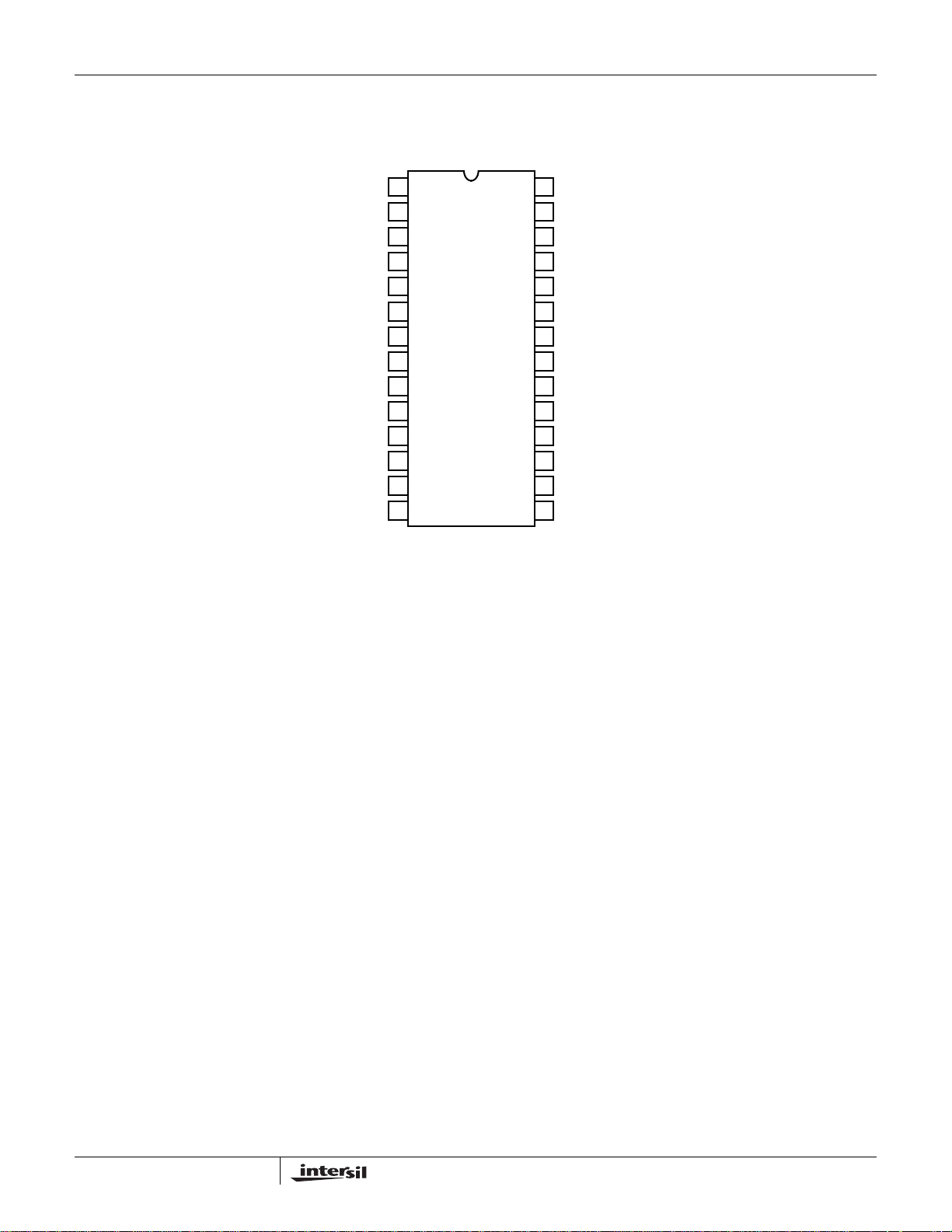
Pinout
GND
LGATE1
PGND1
PHASE1
UGATE1
BOOT1
ISEN1
EN1
VOUT1
VSEN1
OCSET1
SOFT1
DDR
VIN
ISL6225
SSOP-28
TOP VIEW
VCC
1
2
3
4
5
6
7
8
9
10
11
12
13
14
28
27
26
25
24
23
22
21
20
19
18
17
16
15
LGATE2
PGND2
PHASE2
UGATE2
BOOT2
ISEN2
EN2
VOUT2
VSEN2
OCSET2
SOFT2
PG2/REF
PG1
2
FN9049.7
December 28, 2004
Page 3

ISL6225
Absolute Maximum Ratings Thermal Information
Bias Voltage, VCC . . . . . . . . . . . . . . . . . . . . . . . . . . . . . . . . . .+ 6.5V
Input Voltage, V
PHASE, UGATE Voltage . . . . . . . . . . . . . . GND-5V (Note 3) to 33V
. . . . . . . . . . . . . . . . . . . . . . . . . . . . . . . . . . +27.0V
IN
BOOT, ISEN Voltage . . . . . . . . . . . . . . . . . . . . GND-0.3V to +33.0V
BOOT with respect to PHASE . . . . . . . . . . . . . . . . . . . . . . . . .+ 6.5V
All Other Pins. . . . . . . . . . . . . . . . . . . . . . GND -0.3V to V
CC
+ 0.3V
ESD Classification . . . . . . . . . . . . . . . . . . . . . . . . . . . . . . . . . Class 2
Recommended Operating Conditions
Bias Voltage, VCC . . . . . . . . . . . . . . . . . . . . . . . . . . . . . . +5.0V ±5%
Input Voltage, V
Ambient Temperature Range. . . . . . . . . . . . . . . . . . . . -10°C to 85°C
. . . . . . . . . . . . . . . . . . . . . . . . . . . +5.0V to +24.0V
IN
Junction Temperature Range. . . . . . . . . . . . . . . . . . . -10°C to 125°C
CAUTION: Stresses above those listed in “Absolute Maximum Ratings” may cause permanent damage to the device. This is a stress only rating and operation of the
device at these or any other conditions above those indicated in the operational sections of this specification is not implied.
NOTES:
3. 200ns transient.
is measured with the component mounted on a high effective thermal conductivity test board in free air. See Tech Brief TB379 for details.
4. θ
JA
Electrical Specifications Recommended Operating Conditions, Unless Otherwise Noted.
PARAMETER SYMBOL TEST CONDITIONS MIN TYP MAX UNITS
V
SUPPLY
CC
Bias Current I
Shut-down Current I
UVLO
V
CC
Rising V
Falling V
V
IN
Threshold V
CC
Threshold V
CC
Input Voltage Pin Current (Sink) I
Input Voltage Pin Current (Source) I
Shut-down Current I
CC
CCSN
CCU
CCD
VIN
VINO
VINS
OSCILLATOR
PWM1 Oscillator Frequency F
Ramp Amplitude, pk-pk V
Ramp Amplitude, pk-pk V
Ramp Offset V
Ramp/V
Ramp/V
Gain G
IN
Gain G
IN
ROFF
RB1
RB2
REFERENCE AND SOFT-START
Internal Reference Voltage V
REF
Reference Voltage Accuracy -1.0 - +1.0 %
Soft-Start Current During Start-up I
SOFT
Soft-Start Complete Threshold V
LGATEx, UGATEx Open, VSENx forced above
regulation point, DDR = 0, VIN > 5V
C
V
R1
R2
= 16V, by design - 2 - V
IN
V
= 5V, by design - 1.25 - V
IN
By design - 0.5 - V
V
≥ 3V, by design - 125 - mV/V
IN
1 ≤ V
IN
By design - 1.5 - V
ST
Thermal Resistance (Typical, Note 4)
θ
JA
(°C/W)
SSOP Package . . . . . . . . . . . . . . . . . . . . . . . . . . . . 78
Maximum Junction Temperature (Plastic Package) . . . . . . . . 150°C
Maximum Storage Temperature Range. . . . . . . . . . . -65°C to 150°C
Maximum Lead Temperature (Soldering 10s) . . . . . . . . . . . . . 300°C
(SSOP - Lead Tips Only)
-2.23.2mA
--30µA
4.3 4.65 4.75 V
4.1 4.35 4.45 V
10 - 30 µA
--15-30 µA
--1µA
255 300 345 kHz
≤ 3V, by design - 250 - mV/V
-0.9- V
--5- µA
3
FN9049.7
December 28, 2004
Page 4

ISL6225
Electrical Specifications Recommended Operating Conditions, Unless Otherwise Noted. (Continued)
PARAMETER SYMBOL TEST CONDITIONS MIN TYP MAX UNITS
PWM CONVERTERS
Load Regulation 0.0mA < I
VSEN pin bias current I
V
pin input impedance I
OUT
Undervoltage Shut-Down Level V
Overvoltage Shut-Down V
VSEN
VOUT
UVL
OVP1
By design 50 80 120 nA
V
= 5V 40 55 65 kΩ
OUT
Fraction of the set point; ~2µs noise filter 70 - 85 %
Fraction of the set point; ~2µs noise filter 110 - 130 %
GATE DRIVERS
Upper Drive Pull-Up Resistance R
Upper Drive Pull-Down Resistance R
Lower Drive Pull-Up Resistance R
Lower Drive Pull-Down Resistance R
2UGPUPVCC
2UGPDNVCC
2LGPUPVCC
2LGPDNVCC
= 4.5V - 8 15 Ω
= 4.5V - 3.2 5 Ω
= 4.5V - 8 15 Ω
= 4.5V - 1.8 3 Ω
POWER GOOD AND CONTROL FUNCTIONS
Power Good Lower Threshold V
Power Good Higher Threshold V
PGOODx Leakage Current I
PGOODx Voltage Low V
PG-
PG+
PGLKG
PGOODIPGOOD
Fraction of the set point; ~3µs noise filter -13 - -7 %
Fraction of the set point; ~3µs noise filter.
Guaranteed by design.
V
PULLUP
EN - Low (Off) --0.8V
EN - High (On) 2.5 - - V
CCM Enforced (Hysteretic Operation
VOUTX pulled low - - 0.1 V
Inhibited)
Automatic CCM/Hysteretic Operation Enabled VOUTX connected to the output 0.9 - - V
DDR - Low (Off) --0.8V
DDR - High (On) 2.5 - - V
DDR REF Output Voltage V
DDR REF Output Current I
DDREF
DDREF
DDR = 1, I
DDR = 1. Guaranteed by design. - 10 16 mA
< 5.0A; 5.0V < V
VOUT1
< 24.0V -2.0 - +2.0 %
BATT
12 - 16 %
= 5.5V - - 1 µA
= -4mA - 0.5 0.85 V
= 0...10mA 0.99*
REF
V
OC2
V
1.01*
OC2
V
OC2
V
4
FN9049.7
December 28, 2004
Page 5

ISL6225
Functional Pin Description
GND (Pin 1)
Signal ground for the IC.
LGATE1, LGATE2 (Pin 2, 27)
These are outputs of the lower MOSFET drivers.
PGND1, PGND2 (Pin 3, 26)
These pins provide the return connection for lower gate
drivers. These pins are connected to sources of the lower
MOSFETs of their respective converters.
PHASE1, PHASE2 (Pin 4, 25)
The PHASE1 and PHASE2 points are the junction points of
the upper MOSFET sources, output filter inductors, and
lower MOSFET drains. Connect these pins to the respective
converter’s upper MOSFET source.
UGATE1, UGATE2 (Pin 5, 24)
These pins provide the gate drive for the upper MOSFETs.
BOOT1, BOOT2 (Pin 6, 23)
These pins power the upper MOSFET drivers of the PWM
converter. Connect this pin to the junction of the bootstrap
capacitor with the cathode of the bootstrap diode. Anode of
the bootstrap diode is connected to the VCC pin.
ISEN1, ISEN2 (Pin 7, 22)
These pins are used to monitor the voltage drop across the
lower MOSFET for current feedback and overcurrent
protection. For precise current detection these inputs can be
connected to the optional current sense resistors placed in
series with the source of the lower MOSFETs.
EN1, EN2 (Pin 8, 21)
These pins enable operation of the respective converter
when high. When both pins are low, the chip is disabled and
only low leakage current <1µA is taken from V
These pins are to be connected together and switched at the
same time.
VOUT1, VOUT2 (Pin 9, 20)
These pins when connected to the converters’ respective
outputs provide the output voltage inside the chip to reduce
output voltage excursion during HYS/PWM transition. When
connected to ground, these pins command forced
converters operate in continuous conduction mode at all
load levels.
VSEN1, VSEN2 (Pin 10, 19)
These pins are connected to the resistive dividers that set
the desired output voltage. The PGOOD, UVP, and OVP
circuits use this signal to report output voltage status.
and VIN.
CC
SOFT1, SOFT2 (Pin 12, 17)
These pins provide soft-start function for their respective
controllers. When the chip is enabled, the regulated 5µA
pull-up current source charges the capacitor connected from
the pin to ground. The output voltage of the converter follows
the ramping voltage on the SOFT pin.
DDR (Pin 13)
This pin, when high, transforms dual channel chip into
complete DDR memory solution. The OCSET2 pin becomes
an input to provide the required tracking function. The
channel synchronization is changed from out-of-phase to inphase. The PG2/REF pin becomes the output of the VDDQ/
2 buffered voltage that is used as a reference voltage by the
second channel.
VIN (Pin 14)
Provides battery voltage to the oscillator for feed-forward
rejection of the input voltage variation.
When connected to ground via 100kΩ resistor while the
DDR pin is high, this pin commands the out-of-phase 90
channels synchronization for reduced inter-channel
interference.
o
PG1 (Pin 15)
PGOOD1 is an open drain output used to indicate the status
of the output voltage. This pin is pulled low when the first
channel output is not within
±10% of the set value.
PG2/REF (Pin 16)
This pin has a double function depending on the mode the
chip is operating. When the chip is used as a dual channel
PWM controller (DDR = 0), the pin provides a PGOOD2
function for the second channel. The pin is pulled low when
the second channel output is not within
In DDR mode (DDR = 1), this pin serves as an output of the
buffer amplifier that provides VDDQ/2 reference voltage
applied to the OCSET2 pin.
±10% of the set value.
OCSET2 (Pin 18)
In a dual channel application (DDR = 0), a resistor from this
pin to ground sets the overcurrent threshold for the second
controller.
In the DDR application (DDR = 1), this pin sets the output
voltage of the buffer amplifier and the second controller and
should be connected to the center point of a divider from the
VDDQ output.
VCC (Pin 28)
This pin powers the controller.
OCSET1 (Pin 11)
A resistor from this pin to ground sets the overcurrent
threshold for the first controller.
5
FN9049.7
December 28, 2004
Page 6

Generic Application Circuits
ISL6225
+V
+3.3V TO +24V
+V
IN
+3.3V TO +24V
ENABLE
IN
+5V
OCSET1
EN1
EN2
VCC
DDR
OCSET2
PWM1
PWM2
Q1
Q2
L1
C1
V
OUT1
+
Q3
Q4
L2
C2
+1.80V
V
OUT2
+1.20V
+
FIGURE 1. ISL6225 APPLICATION CIRCUIT FOR TWO CHANNEL POWER SUPPLY
ENABLE
+5V
OCSET1
EN1
EN2
VCC
DDR
PG2/VREF
PWM1
PWM2
Q1
Q2
OCSET2
L1
C1
VDDQ
+
Q3
Q4
L2
C2
+2.50V
VTT
+1.25V
+
VREF
+1.25V
FIGURE 2. ISL6225 APPLICATION CIRCUIT FOR COMPLETE DDR MEMORY POWER SUPPLY
6
FN9049.7
December 28, 2004
Page 7
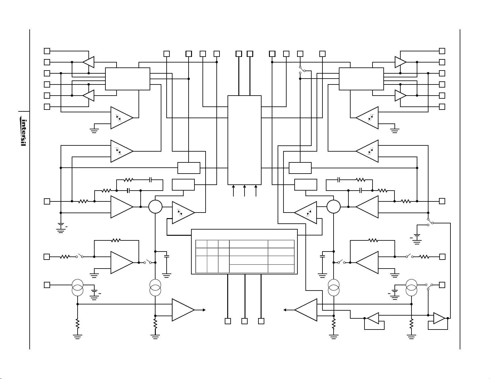
Block Diagram
BOOT1
UGATE1
PHASE1
PGND1
LGATE1
7
VCC
MODE CHANGE COMP 1
HYSTERETIC COMPARATOR 1
VSEN1
300kΩ
ADAPTIVE DEAD-TIME
DIODE EMULATION
V/I SAMPLE TIMING
PWM/HYS TRANSITION
+
-
SAME STATE FOR
8 CLOCK CYCLES
REQUIRED TO CHANGE
PWM OR HYS MODE
-
+
1MΩ
500kΩ
1.3pF
-
∆V
HYS
+
0.9V REFERENCE
+
ERROR AMP 1
=15mV
15.2pF
Σ
SOFT1
OV UV
PGOOD
VOLTS/SEC
CLAMP
-
+
PWM1
VOUT1 VOUT2
DDR EN1 EN2 VIN CH1 CH2
100Ω
ISEN1
OCSET1
CURRENT
SAMPLE
-
+
0.9V REFERENCE
+
CURRENT
SAMPLE
011 0 ⇔ 24.0V 180º
111
VCCPG1
GNDEN1 EN2 REF/PG2
POR
ENABLE
BIAS SUPPLIES
REFERENCE
FAULT LATCH
SOFT-START
DDR MODE
CONTROL
OC1 DDR
DUTY CYCLE RAMP GENERATOR
PWM CHANNEL PHASE CONTROL
OC2
4.2 < VIN < 24.0V
VIN to GND
0º
90º
DDR=0
PGOOD
PWM2
φ
DDR=1
OV UV
VOLTS/SEC
CLAMP
SOFT2
REQUIRED TO CHANGE
-
Σ
+
ADAPTIVE DEAD-TIME
DIODE EMULATION
V/I SAMPLE TIMING
PWM/HYS TRANSITION
SAME STATE FOR
8 CLOCK CYCLES
PWM OR HYS MODE
∆V
=15mV
HYS
15.2pF
ERROR AMP 2
CURRENT
SAMPLE
1MΩ
1.3pF
0.9V REFERENCE
+
MODE CHANGE COMP 2
-
HYSTERETIC COMPARATOR 2
-
+
500kΩ
300kΩ
-
+
0.9V REFERENCE
-
+
+
+
CURRENT
SAMPLE
DDR=0
100Ω
DDR=0
BOOT2
UGATE2
PHASE2
PGND2
LGATE2
VCC
VSEN2
DDR=1
ISEN2
OCSET2
DDR=1
-
December 28, 2004
1/3
FN9049.7
OCSET1
1/32
ISEN1
+
REQUIRED TO LATCH
OVER-CURRENT FAULT
OC1
SAME STATE FOR
8 CLOCK CYCLES
DDR
VIN VCC
OC2
SAME STATE FOR
8 CLOCK CYCLES
REQUIRED TO LATCH
OVER-CURRENT FAULT
-
+
1/32
ISEN2
+
-
DDR VREF
BUFFER AMP
1/3
OCSET2
+
-
DDR VTT
REFERENCE
Page 8
Description
Operation
The ISL6225 is a dual channel PWM controller intended for
use in power supplies for graphic chipset, SDRAM, DDR
DRAM or other low voltage power applications in modern
notebook and sub-notebook PCs. The IC integrates two
control circuits for two synchronous buck converters. The
output voltage of each controller can be set in the range of
0.9V to 5.5V by an external resistive divider. Out-of-phase
operation with 180 degree phase shift reduces input current
ripple.
The synchronous buck converters can operate from either
an unregulated DC source such as a notebook battery with a
voltage ranging from 5.0V to 24V, or from a regulated system
rail of 3.3V or 5V. In either mode of operation the controller is
biased from the +5V source.
The controllers operate in the current mode with input
voltage feed-forward for simplified feedback loop
compensation and reduced effect of the input voltage
variation. An integrated feedback loop compensation
dramatically reduces the number of external components.
Depending on the load level, converters can operate either
in a fixed-frequency mode or in a hysteretic mode. Switchover to the hysteretic mode operation at light loads improves
the converters' efficiency and prolongs battery run time. The
hysteretic mode of operation can be inhibited independently
for each channel if a variable frequency operation is not
desired.
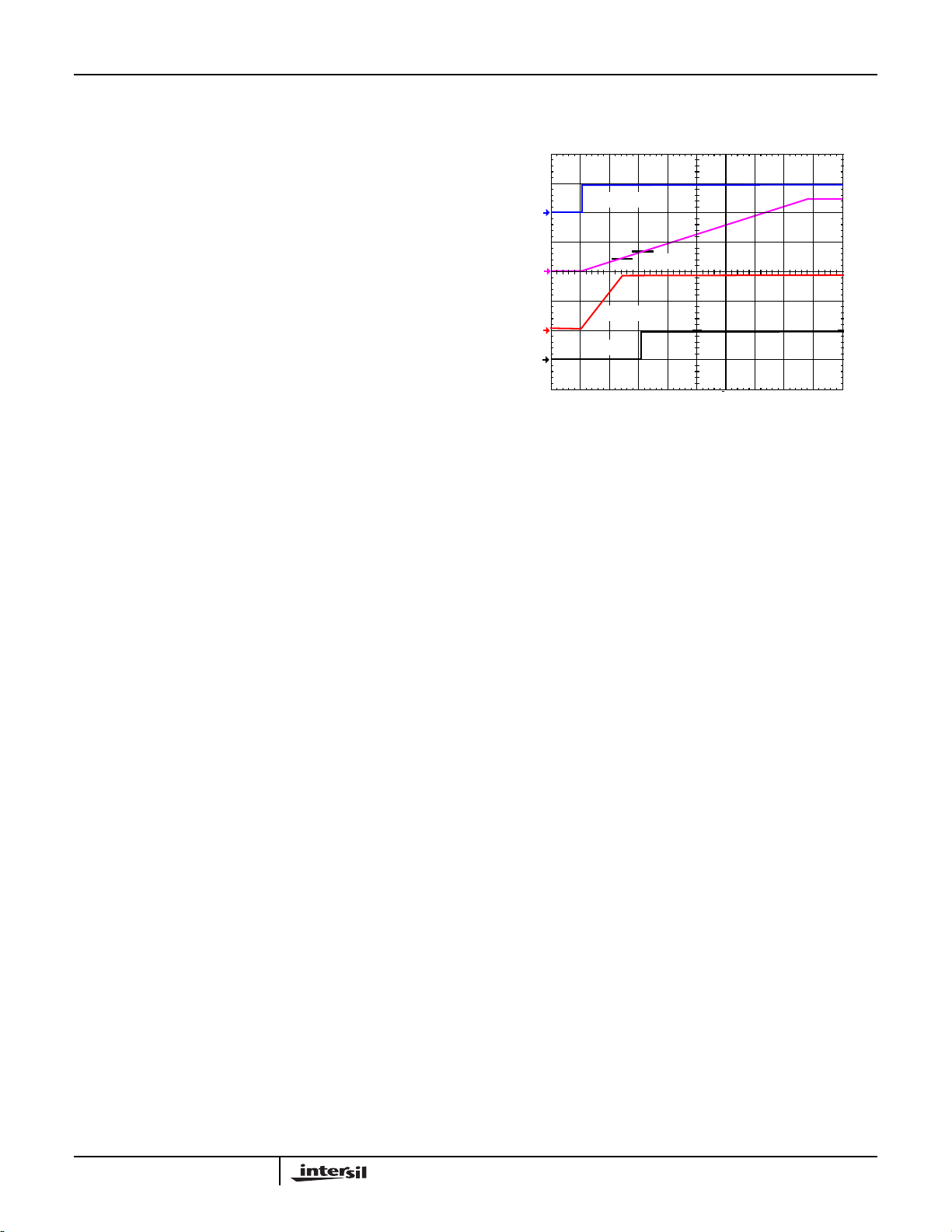
1.5V, the power good (PGOOD), the mode control, and the
fault functions are enabled, as depicted in Figure 3.
1
2
3
4
Ch1 5.0V
Ch3 1.0V
EN
1.5V
0.9V
PGOOD
SOFT
VOUT
Ch2 2.0V
Ch4 5.0V
FIGURE 3. START UP
M1.00ms
This completes the soft-start sequence. Further rise of pin
voltage does not affect the output voltage. During the softstart, the converter always operates in continuous
conduction mode independently of the load level or FCCM
pin potential.
The soft-start time (the time from the moment when EN
becomes high to the moment when PGOOD is reported) is
determined by the following equation.
T
SOFT
1.5V C soft×
----------------------------------=
5µ A
The ISL6225 has a special means to rearrange its internal
architecture into a complete DDR solution. When DDR input
is set high, the second channel can provide the capability to
track the output voltage of the first channel. The buffered
reference voltage required by DDR memory chips is also
provided.
Initialization
The Power-On Reset (POR) function continually monitors
the bias supply voltage on the V
pin and initiates soft-start
CC
operation after the input supply voltage exceeds 4.5V.
Should this voltage drop lower than 4.0V, the POR disables
the chip.
Soft-Start
When soft-start is initiated, the voltage on the SOFT pin
starts to ramp gradually due to the 5
the external soft-start capacitor. The output voltage starts to
follow the soft-start voltage.
When the SOFT pin voltage reaches a level of 0.9V, the
output voltage comes into regulation while the soft-start pin
voltage continues to rise. When the SOFT voltage reaches
µA current sourced into
The time it takes the output voltage to come into regulation
can be obtained from the following equation.
T
RISE
0.6 T
×=
SOFT
Having such a spread between the time when the output
voltage reaches the regulation point and the moment when
PGOOD is reported allows for a fault-safe test mode by
means of an external circuit that clamps the SOFT pin
voltage on the level 0.9V < V
SOFT
< 1.5V.
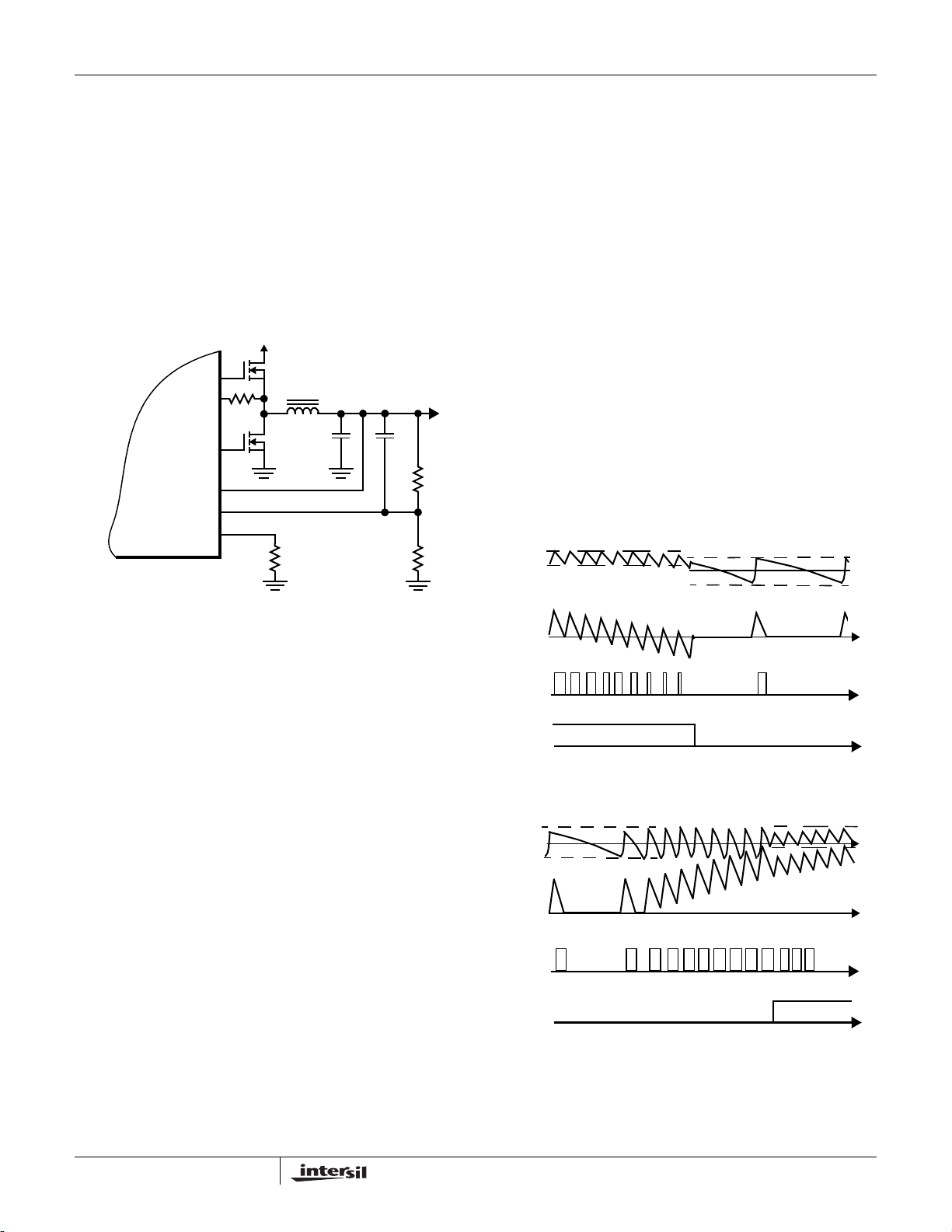
Output Voltage Program
The output voltage of either channel is set by a resistive divider
from the output to ground. The center point of the divider is
connected to VSEN pin as shown in Figure 4. The output
voltage value is determined by the following equation.
0.9V R1 R2+()•
V
----------------------------------------------=
O
Where 0.9V is the value of the internal reference. The VSEN
pin voltage is also used by the controller for the power good
function and to detect Undervoltage and Overvoltage
conditions.
R2
8
FN9049.7
December 28, 2004
Page 9
ISL6225
Automatic Operation Mode Control
In nominal currents the synchronous buck converter
operates in continuous-conduction constant-frequency
mode. This mode of operation achieves higher efficiency
due to the substantially lower voltage drop across the
synchronous MOSFET compared to a Schottky diode.
In contrast, continuous-conduction operation with load
currents lower than the inductor critical value results in lower
efficiency. In this case, during a fraction of a switching cycle,
the direction of the inductor current changes to the opposite,
actively discharging the output filter capacitor.
VIN
UGATE
ISEN
LGATE
VOUT
VSEN
OCSET
ISL6225
Q1
L1
R
CS
Q2
C1
R
OC
Cz
R1
R2
The voltage across the synchronous MOSFET at the
moment of time just before the upper-MOSFET turns on is
monitored for purposes of mode change. When the
converter operates at currents higher than critical, this
voltage is always negative. In currents lower than critical, the
voltage is always positive. The mode control circuit uses a
sign of voltage across the synchronous devices to determine
if the load current is higher or lower than the critical value.
To prevent chatter between operating modes, the circuit
looks for eight contiguous signals of the same polarity before
it makes the decision to perform a mode change. The same
algorithm is true for both CCM-hysteretic and hystereticCCM transitions.
Hysteretic Operation
When the critical inductor current is detected, the converter
enters hysteretic mode. The PWM comparator and the error
amplifier that provided control in the CCM mode are inhibited
and the hysteretic comparator is now activated. A change is
also made to the gate logic. In hysteretic mode the
synchronous rectifier MOSFET is controlled in diode
emulation mode, hence conduction in the second quadrant
is prohibited.
VOUT
t
FIGURE 4. OUTPUT VOLTAGE PROGRAM
To maintain the output voltage in regulation, the discharged
energy should be restored during the consequent cycle of
operation by the cost of increased circulating current and
losses associated with it.
The critical value of the inductor current can be estimated by
the following expression:
VINV
–()V
•
O
I
HYS
=
-----------------------------------------------------
2FSWLOVIN•••
O
To improve converter efficiency at loads lower than critical,
the switch-over to variable frequency hysteretic operation
with diode emulation is implemented into the PWM scheme.
The switch-over is provided automatically by the mode
control circuit that constantly monitors the inductor current
and alters the way the PWM signal is generated.
IIND
PHASE
COMP
MODE
OF
OPERATION
VOUT
IIND
PHASE
COMP
MODE
OF
OPERATION
1 2 3 4 5 6 7 8
PWM
HYSTERETIC
FIGURE 5. CCM - HYSTERETIC TRANSITION
1 2 3 4 5 6 7 8
HYSTERETIC
PWM
FIGURE 6. HYSTERETIC - CCM TRANSITION
t
t
t
t
t
t
t
9
FN9049.7
December 28, 2004
Page 10
ISL6225
The hysteretic comparator initiates the PWM signal when the
output voltage gets below the lower threshold and
terminates the PWM signal when the output voltage rises
above the upper threshold. A spread or hysteresis between
these two thresholds determines the switching frequency
and the peak value of the inductor current. The transition to
constant frequency CCM mode happens when the inductor
current increases above the critical value:
∆V
hys
CCM
----------------------
≈
2ESR•
= 15mV, is a hysteretic comparator window,
hys
I
Where, ∆V
ESR is the equivalent series resistance of the output
capacitor. Because of different control mechanisms, the
value of the load current where transition into CCM
operation takes place is usually higher compared to the load
level at which transition into hysteretic mode had occurred.
V
pin and Forced Continuous
OUT
Conduction Mode (FCCM)
The controller has the flexibility to operate a converter in
fixed-frequency constant conduction mode (CCM), or in
hysteretic mode. Connecting the V
pin to GND will inhibit
OUT
hysteretic mode; this is called forced constant conduction
mode (FCCM). Connecting the V
pin to the converter
OUT
output will allow transition between CCM mode and
hysteretic mode.
When the V
pin is connected to the converter output, a
OUT
circuit is activated that smooths the transition from hysteretic
mode to CCM mode. While in hysteretic mode, this circuit
prepositions the PWM error amplifier output to a level close
to that needed to provide the appropriate PWM duty cycle
required for regulation. This is a much more desirable state
for the PWM error amplifier at mode transition, as opposed
to being in saturation which requires a period of time to slew
to the required level.
Such dual function of the V
pin enhances applicability of
OUT
the controller and allows for lower pin count.
Feedback Loop Compensation
To reduce the number of external components and remove
the burden of determining compensation components from a
system designer, both PWM controllers have internally
compensated error amplifiers. To make internal
compensation possible several design measures where
taken.
First, the ramp signal applied to the PWM comparator is
proportional to the input voltage provided via the VIN pin.
This keeps the modulator gain constant when the input
voltage varies. Second, the load current proportional signal
is derived from the voltage drop across the lower MOSFET
during the PWM
error signal on the comparator input. This effectively creates
time interval and is added to the amplified
an internal current control loop. The resistor connected to
the ISEN pin sets the gain in the current feedback loop. The
following expression estimates the required value of the
current sense resistor depending on the maximum load
current and the value of the MOSFET’s r
I
⋅
R
MAXrDS ON()
----------------------------------------------
CS
75µ A
100Ω–=
DS(ON)
.
Due to implemented current feedback, the modulator has a
single pole response with -1 slope at a frequency
determined by the load,
F
PO
1
----------------------------------=
2π ROC
⋅⋅
O
where: Ro is load resistance and Co is load capacitance. For
this type of modulator, a Type 2 compensation circuit is
usually sufficient.
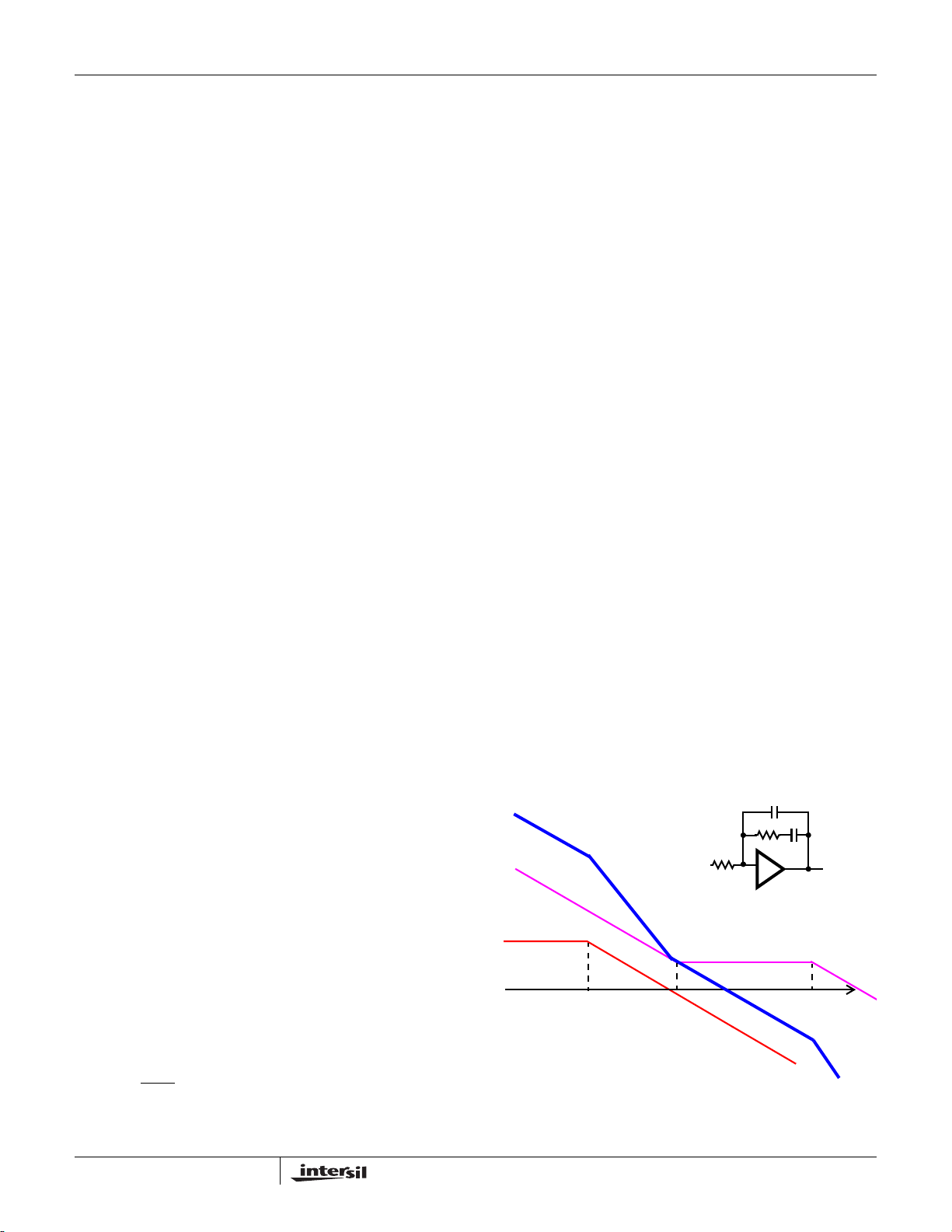
Figure 7 shows a Type 2 amplifier and its response along
with the responses of the current mode modulator and the
converter. The Type 2 amplifier, in addition to the pole at
origin, has a zero-pole pair that causes a flat gain region at
frequencies between the zero and the pole:
F
Z
;
F
P
1
------------------------------- 6kHz==
2π R2C
⋅⋅
1
1
------------------------------- 600 kHz==
2π R1C
⋅⋅
2
This region is also associated with phase ‘bump’ or
reduced phase shift. The amount of phase shift reduction
depends on how wide the region of flat gain is and has a
maximum value of 90
o
. To further simplify the converter
compensation, the modulator gain is kept independent of
the input voltage variation by providing feed-forward of V
IN
to the oscillator ramp.
C2
C1
R1
G
F
C
R2
TYPE 2 EA
= 14dB
EA
F
P
CONVERTER
EA
= 18dB
G
M
MODULATOR
F
Z
F
PO
FIGURE 7. FEEDBACK LOOP COMPENSATION
10
FN9049.7
December 28, 2004
Page 11
ISL6225
The zero frequency, the amplifier high-frequency gain, and
the modulator gain are chosen to satisfy most typical
applications. The crossover frequency will appear at the
point where the modulator attenuation equals the amplifier
high frequency gain. The only task that the system designer
has to complete is to specify the output filter capacitors to
position the load main pole somewhere within one decade
lower than the amplifier zero frequency. With this type of
compensation plenty of phase margin is easily achieved due
to zero-pole pair phase ‘boost’. Conditional stability may
occur only when the main load pole is positioned too much
to the left side on the frequency axis due to excessive output
filter capacitance. In this case, the ESR zero placed within
10kHz...50kHz range gives some additional phase ‘boost’.
Some phase boost can also be achieved by connecting
capacitor C
in parallel with the upper resistor R1 of the
z
divider that sets the output voltage value, as shown in
Figure 4.
Gate Control Logic
The gate control logic translates generated PWM signals
into gate drive signals providing necessary amplification,
level shift, and shoot-trough protection. Also, it bears some
functions that help to optimize the IC performance over a
wide range of the operational conditions. As MOSFET
switching time can very dramatically from type to type and
with the input voltage, the gate control logic provides
adaptive dead time by monitoring real gate waveforms of
both the upper and the lower MOSFETs.
Dual-Step Conversion
The ISL6225 dual channel controller can be used either in
power systems with a single-stage power conversion when
the battery power is converted into the desired output
voltage in one step, or in the systems where some
intermediate voltages are initially established. The choice of
the approach may be dictated by the overall system design
criteria or simply to be a matter of voltages available to the
system designer, like in the case of PCI card applications.
When the power input voltage is a regulated 5V or 3.3V
system bus, the feed-forward ramp may become too
shallow, which creates the possibility of duty-factor jitter
especially in a noisy environment. The noise susceptibility
when operating from low level regulated power sources can
be improved by connecting the VIN pin to ground. The feedforward ramp generator will be internally reconnected from
the VIN pin to the V
doubled. Application circuits for dual-step power conversion
are presented in Figures 11 through 15.
pin and the ramp slew rate will be
CC
Protections
The converter output is monitored and protected against
extreme overload, short circuit, Overvoltage, and
Undervoltage conditions.
A sustained overload on the output sets the PGOOD low and
latches-off the whole chip. The controller operation can be
restored by cycling the VCC voltage or an enable (EN) pin.
Overcurrent Protection
Both PWM controllers use the lower MOSFET’s
on-resistance {r
against shorted outputs. The sensed current from the ISEN
pin is compared with a current set by a resistor connected
from the OCSET pin to ground.
R
OCSET
Where, I
R
is the value of the current sense resistor connected to
CS
the I
SEN
9.6V R
----------------------------------------------------------=
is a desired overcurrent protection threshold and
OC
pin.
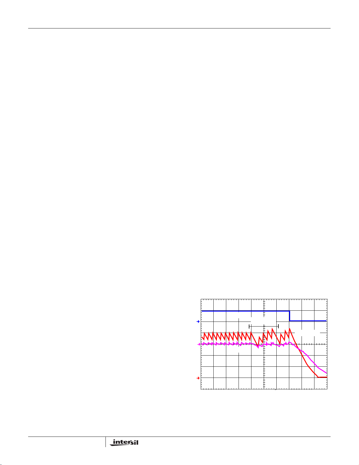
If the lower MOSFET current exceeds the overcurrent
threshold, a pulse skipping circuit is activated. The upper
MOSFET will not be turned on as long as the sensed
current is higher then the threshold value. This limits the
current supplied by the DC voltage source. This condition
keeps on for eight clock cycles after the overcurrent
comparator was tripped for the first time. If after these first
eight clock cycles the current exceeds the overcurrent
threshold again in a time interval of another eight clock
cycles, the overcurrent protection latches and disables the
chip. If the overcurrent condition goes away during the first
eight clock cycles, normal operation is restored and the
overcurrent circuit resets itself sixteen clock cycles after the
overcurrent threshold was exceeded the first time, Figure 8.
1
IL
2
3
} to monitor the current for protection
DS(ON)
100Ω+()•
CS
I
R•
OC
DS ON()
PGOOD
8 CLK
VOUT
SHUTDOWN
11
CH1 5.0V
CH3 1.0AΩ
FIGURE 8. OVERCURRENT PROTECTION WAVEFORMS
CH2 100mV
M 10.0µs
FN9049.7
December 28, 2004
Page 12

ISL6225
If load step is strong enough to pull output voltage lower
than the undervoltage threshold, the chip shuts down
immediately.
Because of the nature of the used current sensing
technique, and to accommodate wide range of the r
variation, the value of the overcurrent threshold should
represent overload current about 150%...180% of the
nominal value. If more precise current protection is desired,
a current sense resistor placed in series with the lower
MOSFET source may be used.
DS(ON)
Overvoltage Protection
Should the output voltage increase over 115% of the normal
value due to the upper MOSFET failure, or other reasons,
the overvoltage protection comparator will force the
synchronous rectifier gate driver high. This action actively
pulls down the output voltage and eventually attempts to
blow the battery fuse. As soon as the output voltage drops
below the threshold, the OVP comparator is disengaged.
This OVP scheme provides a ‘soft’ crowbar function which
helps to tackle severe load transients and does not invert the
output voltage when activated - a common problem for OVP
schemes with a latch.
The ISL6225 dual channel PWM controller possesses
several important means that allow reconfiguration for this
particular application and provide all three voltages required
in DDR memory-compliant computer.
To reconfigure the ISL6225 for a complete DDR solution, the
DDR pin shall be permanently set high. The simplest way to
do that is to connect it to the V
functions inside the chip that are specific to the DDR
memory power needs.
In the DDR application presented in Figures 14 and 15, the
first controller regulates the VDDQ rail to 2.5V. The output
voltage is set by an external divider R3 and R5. The second
controller regulates the VTT rail to VDDQ/2. The OCSET2
pin function is now different. The pin serves now as an input
that brings VDDQ/2 voltage created by R4 and R6 divider
inside the chip. That effectively provides a tracking function
for the VTT voltage.
The PG2 pin function is also different in DDR mode. This pin
becomes the output of the buffer, which input is connected
via the OCSET2 pin to the center point of the R/R divider
from the VDDQ output. The buffer output voltage serves as
1.25V reference for the DDR memory chips. Current
capability of this pin is about 10mA.
rail. This activates some
CC
Over-Temperature Protection
The chip incorporates an over-temperature protection circuit
that shuts the chip down when the die temperature of 150°C
is reached. Normal operation restores at die temperatures
below 125°C through the full soft-start cycle.
DDR Application
Double Data Rate (DDR) memory chips are expected to take
the place of traditional memory in many newly designed
computers, including high-end notebooks, due to increased
throughput. A novel feature associated with this type of
memory is new referencing and data bus termination
techniques. These techniques employ a reference voltage,
VREF, that tracks the center point of VDDQ and VSS
voltages and an additional VTT power source to which all
terminating resistors are connected. Despite the additional
power source, the overall memory power consumption is
reduced compared to traditional termination.
The added power source has a cluster of requirements that
should be observed and considered. Due to reduced
differential thresholds of DDR memory, the termination
power supply voltage, VTT, shall closely track VDDQ/2
voltage. Another very important feature for the termination
power supply is a capability to equally operate in sourcing
and sinking modes. The VTT supply shall regulate the output
voltage with the same degree of precision when current is
floating from the supply to the load and when the current is
diverted back from the load into the power supply. The last
mode of operation usually conflicts with the way most PWM
controllers operate.
For the VTT channel some control and protective functions
can be significantly simplified as this output is derived from
the VDDQ output. For example, the overcurrent and
overvoltage protections for the second controller are
disabled when the DDR pin is set high. The hysteretic mode
of operation is also disabled on the VTT channel to allow
sinking capability to be independent from the load level. As
the VTT channel tracks the VDDQ/2 voltage, the soft-start
function is not required and the SOFT2 pin may be left open.
Channel Synchronization in DDR
Applications
Presence of two PWM controllers on the same die require
channel synchronization to reduce inter channel interference
that may cause the duty factor jitter and increased output
ripple. The PWM controller is mostly susceptible to noise
when an error signal on the input of the PWM comparator
approaches the decision making point. False triggering can
occur causing jitter and affecting the output regulation.
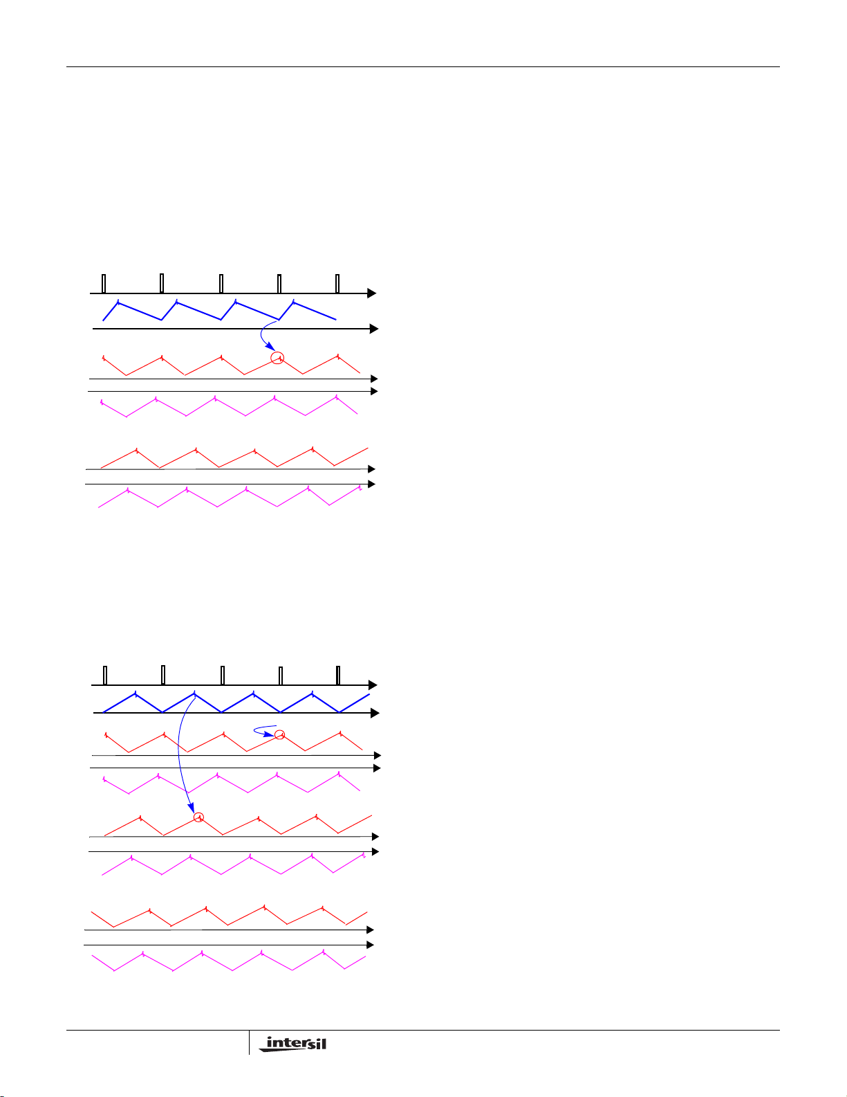
Out-of-phase operation is a common approach to
synchronize dual channel converters as it reduces an input
current ripple and provides a minimum interference for
channels that control different voltage levels. When used in
DDR application with cascaded converters (VTT generated
from VDDQ), the turn-on of the upper MOSFET in the VDDQ
channel happens to be just before the decision making point
in the VTT channel that is running with a duty-factor close to
50%, as in Figure 10.
12
FN9049.7
December 28, 2004
Page 13
ISL6225
This makes out-of-phase channel synchronization
undesirable when one of the channels is running on a dutyfactor of 50%. Inversely, the in-phase channel arrangement
does not have this drawback. Points of decision are far from
noisy moments of time in both sourcing and sinking modes
of operation for V
= 7.5V to 24V as it is shown in Figure 9.
IN
In the case when power for VDDQ is taken from the +5V
system rail, as Figure 10 shows, both in-phase and out-ofphase approaches are susceptible to noise in the sourcing
mode.
300kHz CLOCK
VDDQ
SOURCING
VTT
SINKING
SOURCING
VTT
SINKING
FIGURE 9. CHANNEL INTERFERENCE VIN = 7.5V...24V
OUT-OF-PHASE
IN-PHASE
Noise immunity can be improved by operating the VTT
converter with a 90
o
phase shift. As the time diagrams in
Figure 10 show, the points of concern are always about a
quarter of the period away from the noise emitting
transitions.
300kHz CLOCK
VDDQ
SOURCING
Several ways of synchronization are implemented into the
chip. When the DDR pin is connected to GND, the channels
operate 180
pin is connected to V
phase when the V
source, or with 90
o
out-of-phase. In the DDR mode when the DDR
, the channels operate either in-
CC
pin is connected to the input voltage
IN
o
phase shift if the VIN pin is connected to
GND.
ISL6225 DC-DC Converter Application
Circuits
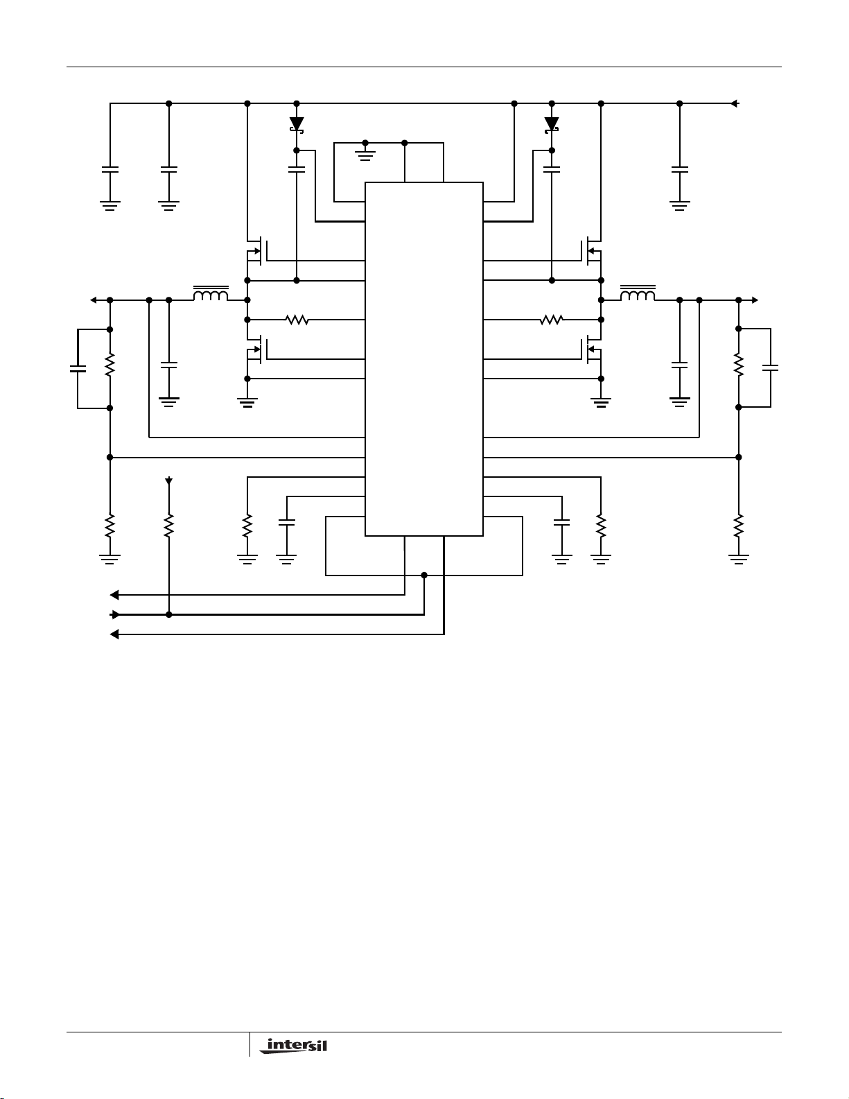
Figures 11 and 12 show application circuits of a dual channel
DC/DC converter for a notebook PC.
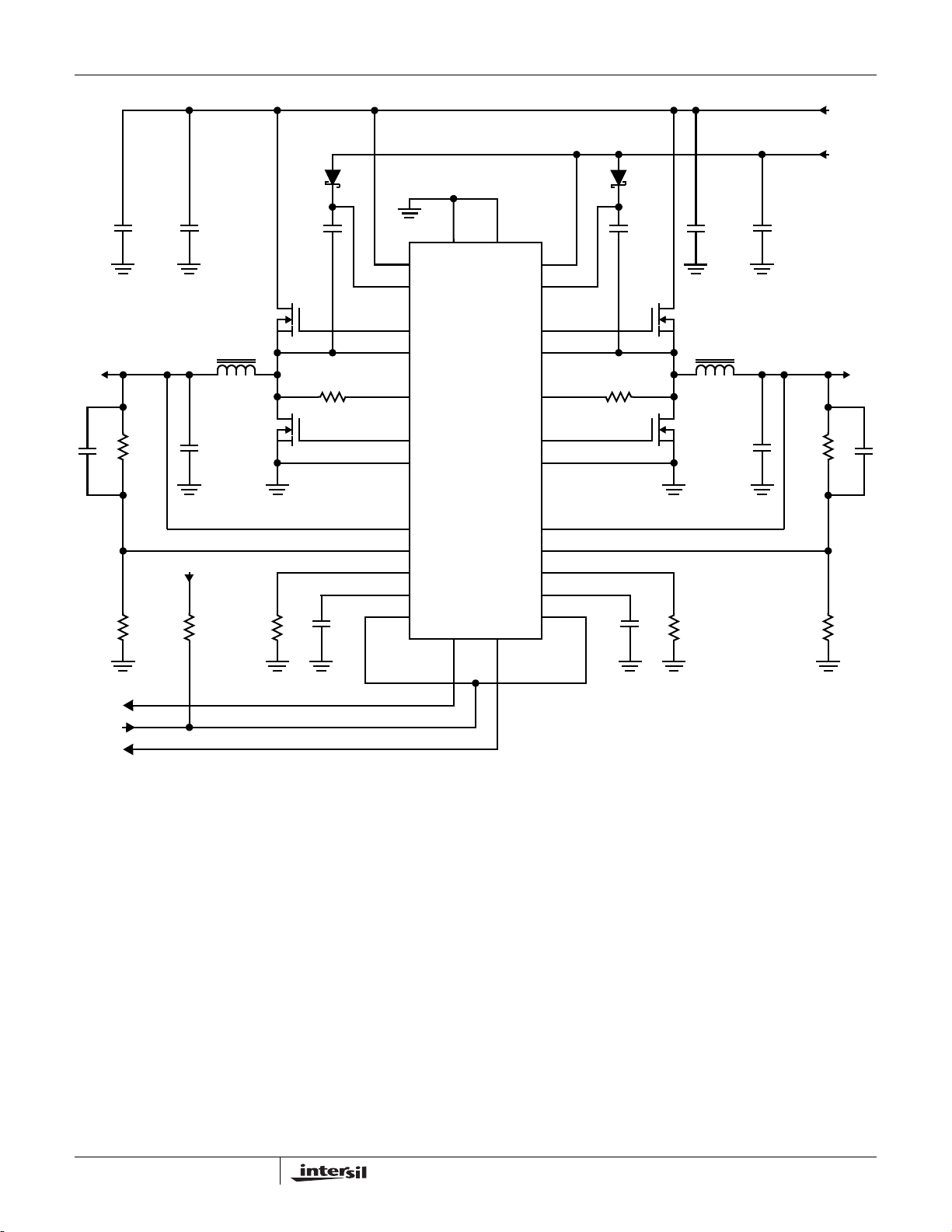
The power supply in Figure 11 provides +2.5V and +1.8V for
memory and graphic interface chipset from +5.0V to +24V
battery voltage.
Figure 12 shows the power supply that provides +2.5V and
+1.8V for memory and graphic interface chipset from +5.0V
system rail.
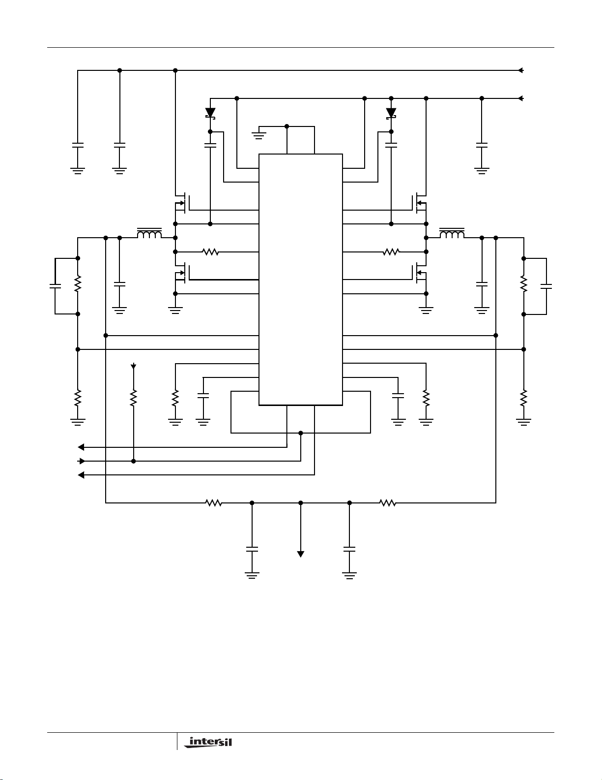
Figure 13 shows an application circuit for a single-output
split input power supply with current sharing for advanced
graphic card applications.
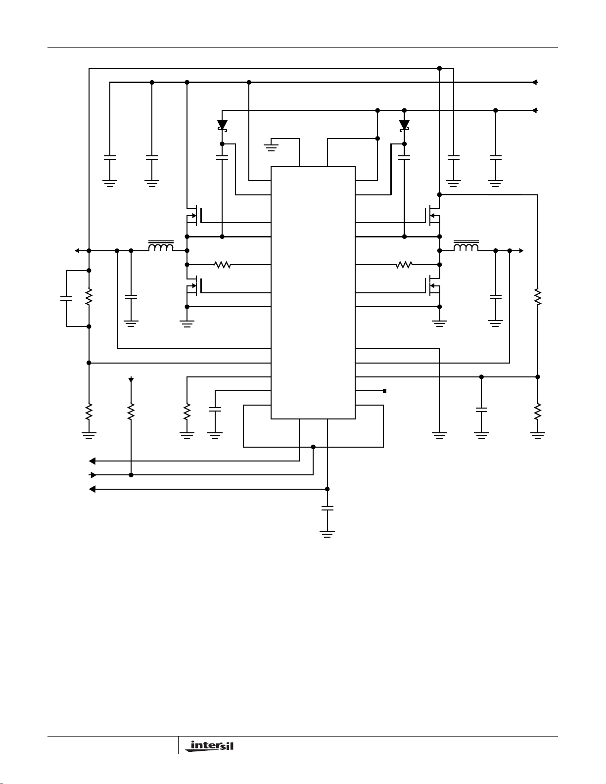
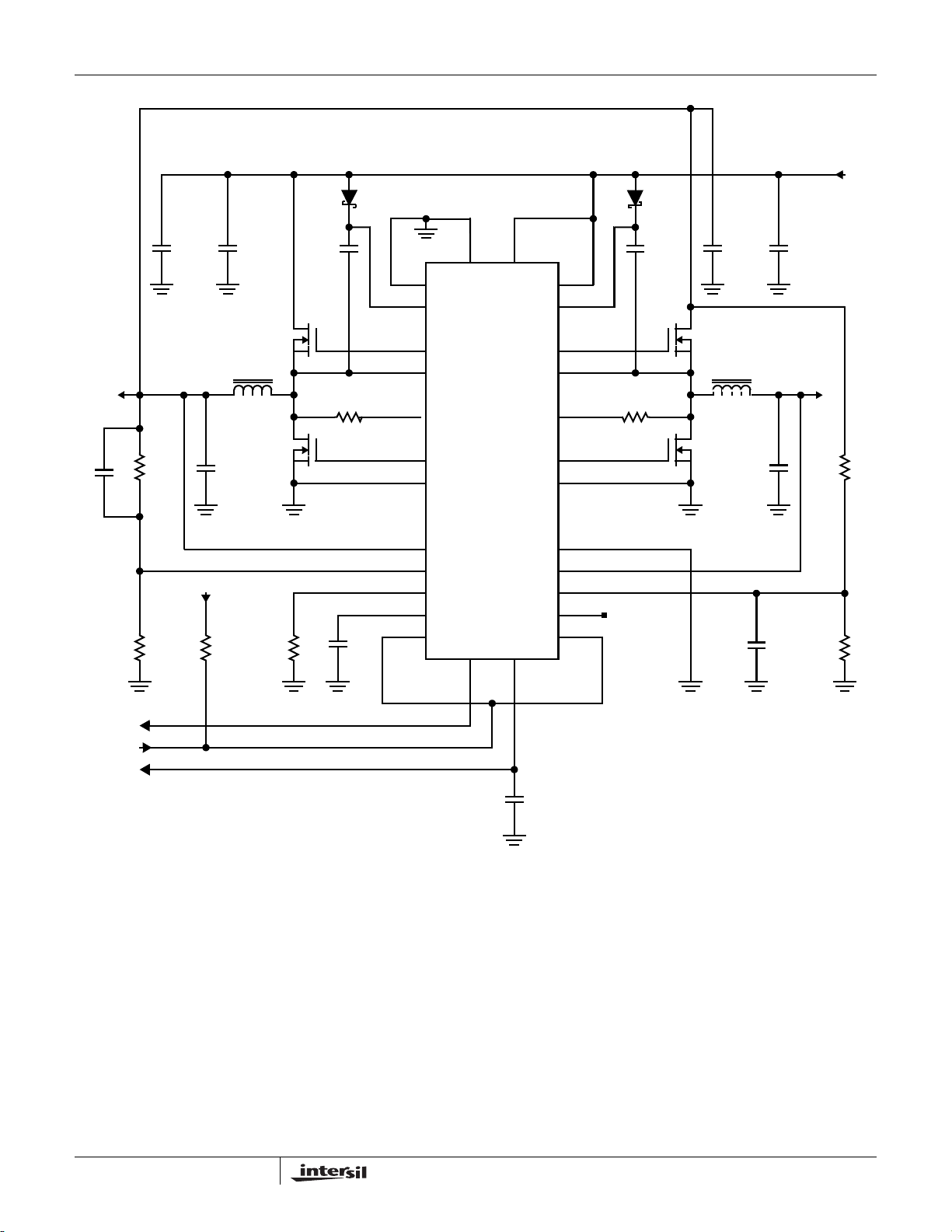
Figure 14 and 15 show application circuits of a complete
power solution for DDR memory that becomes a preferred
choice in modern computers. The power supply shown in
Figure 14 generates +2.5V VDDQ voltage from +5.0V to
+24V battery voltage. The +1.25V VTT termination voltage
tracks VDDQ/2 and is derived from +2.5V VDDQ. To
complete the DDR memory power requirements, the +1.25V
reference voltage is also provided. The PG2 pin serves as
an output for the reference voltage in this mode.
Figure 15 depicts the DDR solution in the case where the 5V
system rail is used as a primary voltage source.
For detailed information on the circuit, including a Bill-ofMaterials and circuit board description, see Application Note
AN9995. Also see Intersil’s web site (http://www.intersil.com)
for the latest information.
VTT
SINKING
SOURCING
VTT
SINKING
SOURCING
VTT
SINKING
FIGURE 10. CHANNEL INTERFERENCE VIN = 5V
OUT-OF-PHASE
IN-PHASE
90o PHASE SHIFT
13
FN9049.7
December 28, 2004
Page 14
C1
1.0µF
ISL6225
VIN
+5.0V TO +24V
VCC
+
+5V
C5
10µF
CR1
BAT54
WT1
+
C2
10µF
C6
0.15µF
VIN
BOOT1
GND
14
6
DDR
13
1
VCC
28
BOOT2
23
CR2
BAT54
WT1
C7
0.15µF
+
C10
10µF
C11
15nF
+2.50V
3.0A
R3
R5
10K
+
VPULLUP
L1
10µH
C8
330µF17.8K
R9
100K
POWER GOOD CH1
ENABLE
POWER GOOD CH2
Q1
1/2 FDS6912A
R1
2.00K
Q2
2/2 FDS6912A
R7
100K
C3
10nF
UGATE1
PHASE1
ISEN1
LGATE1
PGND1
VOUT1
VSEN1
OCSET1
SOFT1
EN1
5
4
7
2
3
9
10
11
12
8
PG1
ISL6225
15
16
PG2/REF
UGATE2
24
PHASE2
25
ISEN2
22
LGATE2
27
PGND2
26
VOUT2
20
VSEN2
19
OCSET2
18
SOFT2
17
EN2
21
Q3
1/2 FDS6912A
R2
2.00K
Q4
2/2 FDS6912A
C4
10nF
100K
R8
L2
10µH
330µF
C9
+1.80V
2.0A
+
R4
10K
R6
10K
C12
15nF
FIGURE 11. DUAL OUTPUT APPLICATION CIRCUIT FOR ONE-STEP CONVERSION
14
FN9049.7
December 28, 2004
Page 15
C1
1.0µF
+
C2
10µF
CR1
BAT54
WT1
C6
0.15µF
VIN
BOOT1
ISL6225
GND
1
14
6
13
DDR
VCC
+
+5V
C5
10µF
CR2
BAT54
WT1
C7
0.15µF
VCC
28
BOOT2
23
C11
15nF
+2.50V
3.0A
R3
R5
10K
+
VPULLUP
R9
100K
L1
4.7µH
C8
330µF17.8K
POWER GOOD CH1
ENABLE
POWER GOOD CH2
Q1
1/2 FDS6912A
R1
2.00K
Q2
2/2 FDS6912A
C3
10nF
100K
UGATE1
PHASE1
ISEN1
LGATE1
PGND1
VOUT1
VSEN1
OCSET1
SOFT1
EN1
5
4
7
2
3
9
10
11
12
8
PG1
ISL6225
15
16
PG2/REF
24
25
22
27
26
20
19
18
17
21
UGATE2
PHASE2
ISEN2
LGATE2
PGND2
VOUT2
VSEN2
OCSET2
SOFT2
EN2
Q3
1/2 FDS6912A
R2
2.00K
Q4
2/2 FDS6912A
C4R7
10nF
100K
R8
L2
4.7µH
330µF
C9
+1.80V
2.0A
+
10K
R6
10K
R4
C12
15nF
FIGURE 12. DUAL OUTPUT APPLICATION CIRCUIT FOR TWO-STEP CONVERSION
15
FN9049.7
December 28, 2004
Page 16
C1
1.0µF
+
C2
10µF
CR1
BAT54
WT1
C6
0.15µF
VIN
BOOT1
ISL6225
GND
1
14
6
13
DDR
VIN
+12V
VCC
+
+5V
C5
10µF
CR2
BAT54
WT1
C7
0.15µF
VCC
28
BOOT2
23
C12
15nF
R3
R5
10K
L1
+
C8
330µF6.65K
VPULLUP
R9
100K
POWER GOOD CH1
ENABLE
POWER GOOD CH2
Q1
1/2 FDS6912A
R1
2.00K
Q2
2/2 FDS6912A
100K
C3
10nF
UGATE1
PHASE1
ISEN1
LGATE1
PGND1
VOUT1
VSEN1
OCSET1
SOFT1
EN1
5
4
7
ISL6225
2
3
9
10
11
12
8
15
16
PG1
24
25
22
27
26
20
19
18
17
21
PG2/REF
UGATE2
PHASE2
ISEN2
LGATE2
PGND2
VOUT2
VSEN2
OCSET2
SOFT2
EN2
Q3
1/2 FDS6912A
R2
2.00K
Q4
2/2 FDS6912A
C4R7
10nF
100K
R8
4.7µH10µH
L2
330µF
C9
+
R4
6.65K
R6
10K
C13
15nF
R10
0.01
+
C10
330µF
+1.50V
8.0A
FIGURE 13. SINGLE-OUTPUT SPLIT INPUT POWER SUPPLY
16
+
C11
330µF
R11
0.01
FN9049.7
December 28, 2004
Page 17
C1
1.0µF
ISL6225
VIN
+5.0V to +24V
VCC
+
+5V
C5
10µF
CR1
BAT54
WT1
+
C2
10µF
C6
0.15µF
VIN
BOOT1
14
6
GND
DDR
13
1
VCC
28
BOOT2
23
CR2
BAT54
WT1
C7
0.15µF
+
C11
10µF
+2.50V
3.0A
VDDQ
C12
15nF
~ 6.0A
R3
17.8K
R5
10K
+
VPULLUP
R9
100K
L1
4.6µH
C8
330µF
POWER GOOD CH1
ENABLE
VREF
Q1
1/2 FDS6912A
R1
2.49K
Q2
2/2 FDS6912A
R7
100K
C3
10nF
UGATE1
PHASE1
ISEN1
LGATE1
PGND1
VOUT1
VSEN1
OCSET1
SOFT1
EN1
5
4
7
2
3
9
10
11
12
8
PG1
ISL6225
15
16
PG2/REF
24
25
22
27
26
20
19
18
17
21
UGATE2
PHASE2
ISEN2
LGATE2
PGND2
VOUT2
VSEN2
OCSET2
SOFT2
EN2
Q3
1/2 FDS6912A
R2
1.00K
Q4
2/2 FDS6912A
L2
1.5µH
330µF
C9
+
C10
10nF
+1.25V
3.0A
VTT
R4
10K
R6
10K
C4
4.7µF
FIGURE 14. APPLICATION CIRCUIT FOR COMPLETE DDR MEMORY POWER SOLUTION WITH ONE-STEP CONVERSION
17
December 28, 2004
FN9049.7
Page 18
C1
1.0µF
+
C2
10µF
CR1
BAT54
WT1
C6
0.15µF
VIN
BOOT1
ISL6225
GND
1
14
6
13
DDR
VCC
CR2
BAT54
WT1
C7
0.15µF
VCC
28
BOOT2
23
+
C10
10µF
+5V
+
C11
10µF
+2.50V
3.0A
VDDQ
C12
15nF
R3
R5
10K
~ 6.0A
VPULLUP
L1
4.6µH
+
C8
330µF17.8K
R9
100K
POWER GOOD CH1
ENABLE
VREF
Q1
1/2 FDS6912A
R1
2.49K
Q2
2/2 FDS6912A
R7
100K
C3
10nF
UGATE1
PHASE1
ISEN1
LGATE1
PGND1
VOUT1
VSEN1
OCSET1
SOFT1
EN1
5
4
7
2
3
9
10
11
12
8
PG1
ISL6225
15
16
PG2/REF
24
25
22
27
26
20
19
18
17
21
UGATE2
PHASE2
ISEN2
LGATE2
PGND2
VOUT2
VSEN2
OCSET2
SOFT2
EN2
Q3
1/2 FDS6912A
R2
1.00K
Q4
2/2 FDS6912A
L2
1.5µH
330µF
C9
+
C5
10nF
+1.25V
3.0A
VTT
R4
10K
R6
10K
C4
4.7µF
FIGURE 15. APPLICATION CIRCUIT FOR COMPLETE DDR MEMORY POWER SOLUTION WITH TWO-STEP CONVERSION
18
December 28, 2004
FN9049.7
Page 19
ISL6225
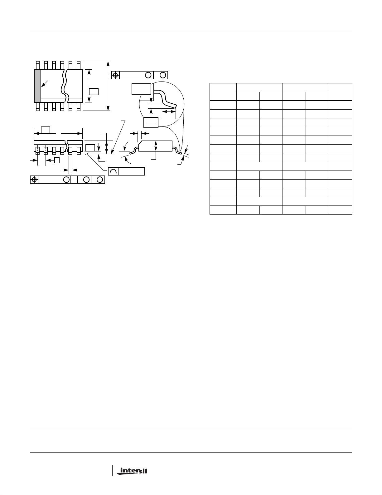
Shrink Small Outline Plastic Packages (SSOP)
Quarter Size Outline Plastic Packages (QSOP)
N
INDEX
AREA
123
-A-
E
-B-
SEATING PLANE
D
A
-C-
0.25(0.010) BM M
H
GAUGE
PLANE
0.25
0.010
h x 45°
L
α
e
B
0.17(0.007) C AM BS
M
A1
0.10(0.004)
NOTES:
1. Symbols are defined in the “MO Series Symbol List” in Section 2.2
of Publication Number 95.
2. Dimensioning and tolerancing per ANSI Y14.5M-1982.
3. Dimension “D” does not include mold flash, protrusions or gate
burrs. Mold flash, protrusion and gate burrs shall not exceed
0.15mm (0.006 inch) per side.
4. Dimension “E” does not include interlead flash or protrusions. Interlead flash and protrusions shall not exceed 0.25mm (0.010 inch)
per side.
5. The chamfer on the body is optional. If it is not present, a visual index feature must be located within the crosshatched area.
6. “L” is the length of terminal for soldering to a substrate.
7. “N” is the number of terminal positions.
8. Terminal numbers are shown for reference only.
9. Dimension “B” does not include dambar protrusion. Allowable dambar protrusion shall be 0.10mm (0.004 inch) total in excess of “B”
dimension at maximum material condition.
10. Controlling dimension: INCHES. Converted millimeter dimensions
are not necessarily exact.
A2
C
M28.15
28 LEAD SHRINK SMALL OUTLINE PLASTIC PACKAGE
(0.150” WIDE BODY)
INCHES MILLIMETERS
SYMBOL
A 0.053 0.069 1.35 1.75 -
A1 0.004 0.010 0.10 0.25 -
A2 - 0.061 - 1.54 -
B 0.008 0.012 0.20 0.30 9
C 0.007 0.010 0.18 0.25 -
D 0.386 0.394 9.81 10.00 3
E 0.150 0.157 3.81 3.98 4
e 0.025 BSC 0.635 BSC -
H 0.228 0.244 5.80 6.19 -
h 0.0099 0.0196 0.26 0.49 5
L 0.016 0.050 0.41 1.27 6
N28 287
α
0° 8° 0° 8° -
NOTESMIN MAX MIN MAX
Rev. 1 6/04
All Intersil U.S. products are manufactured, assembled and tested utilizing ISO9000 quality systems.
Intersil Corporation’s quality certifications can be viewed at www.intersil.com/design/quality
Intersil products are sold by description only. Intersil Corporation reserves the right to make changes in circuit design, software and/or specifications at any time without
notice. Accordingly, the reader is cautioned to verify that data sheets are current before placing orders. Information furnished by Intersil is believed to be accurate and
reliable. However, no responsibility is assumed by Intersil or its subsidiaries for its use; nor for any infringements of patents or other rights of third parties which may result
from its use. No license is granted by implication or otherwise under any patent or patent rights of Intersil or its subsidiaries.
For information regarding Intersil Corporation and its products, see www.intersil.com
19
FN9049.7
December 28, 2004
 Loading...