

Page 1
®
ISL6228
Data Sheet May 7, 2008
High-Performance Dual-Output Buck
Controller for Notebook Applications
The ISL6228 IC is a dual channel synchronous-buck PWM
controller featuring Intersil's Robust Ripple Regulator (R
technology that delivers truly superior dynamic response to
input voltage and output load transients. Integrated
MOSFET drivers and bootstrap diodes result in fewer
components and smaller implementation area.
Intersil’s R
3
technology combines the best features of fixedfrequency and hysteretic PWMs while eliminating many of
their shortcomings. R
3
technology employs an innovative
modulator that synthesizes an AC ripple voltage signal V
analogous to the output inductor ripple current. The AC signal
V
enters a window comparator where the lower threshold is
R
the error amplifier output V
programmable voltage reference V
of the PWM signal. The voltage reference V
, and the upper threshold is a
COMP
resulting in generation
W,
sets the
W
steady-state PWM frequency. Both edges of the PWM can be
modulated in response to input voltage transients and output
load transients, much faster than conventional fixedfrequency PWM controllers. Unlike a conventional hysteretic
converter, each channel of the ISL6228 has an error a mplifier
that provides ±1% voltage regulation at the FB pin.
The ISL6228 has a 1.5ms digital soft-start and can be
started into a pre-biased output voltage. A resistor divider is
used to program the output voltage setpoint. The ISL6228
operates in continuous-conduction-mode (CCM) in heavy
load, and in diode-emulation-mode (DEM) in light load to
improve light-load efficiency. In CCM, the controller always
operates as a synchronous rectifier. In DEM, the low-side
MOSFET is permitted to stay off, blocking negative current
flow into the low-side MOSFET from the output inductor.
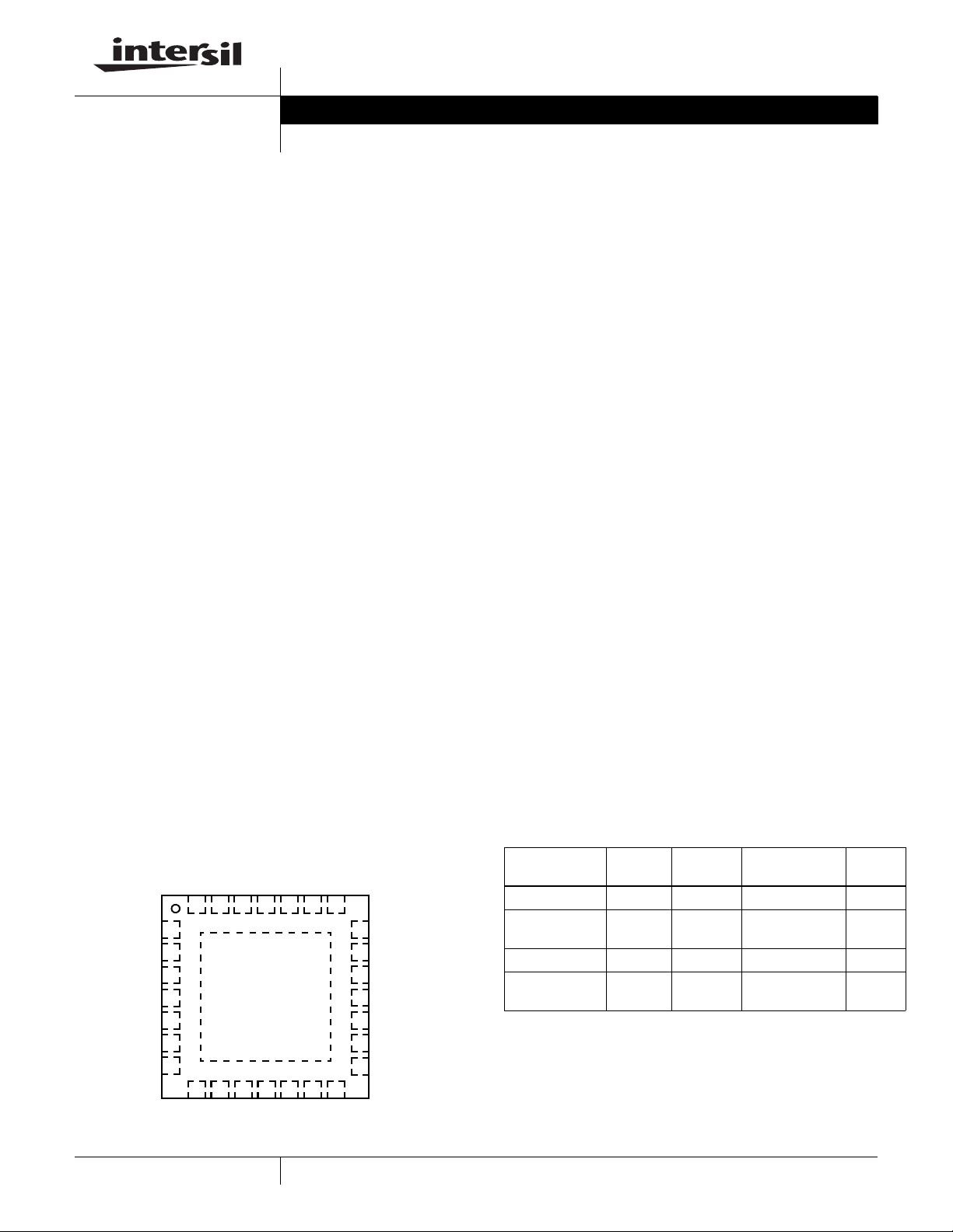
Pinout
FSET2
VIN2
VCC2
VCC1
VIN1
FSET1
PGOOD1
ISL6228 (28 LD 4x4 TQFN)
28
1
2
3
4
5
6
7
FB2
PGOOD2
27 24
8
912
FB1
VO1
OCSET2
VO2
25
26
GND
11
10
EN1
OCSET1
EN2
PHASE1
PHASE2
UGATE2
23
22
21
20
19
18
17
16
15
13
14
BOOT1
UGATE1
BOOT2
PVCC2
LGATE2
PGND2
PGND1
LGATE1
PVCC1
3
)
,
R
FN9095.2
Features
• High performance R3 technology
• Fast transient response
• ±1% regulation accuracy: -40°C to +100°C
• Individual power stage input rail for each channel
• Wide input voltage range: +3.3V to +25V
• Output voltage range: +0.6V to +5V
• Diode emulation mode for increased light load efficiency
• Programmable PWM frequency: 200kHz to 600kHz
• Pre-biased output start-up capability
• Integrated MOSFET drivers and bootstrap diode
• Internal digital soft-start
• Power good monitor
• Fault protection
- Undervoltage protection
- Soft crowbar overvoltage protection
- Inductor DCR overcurrent protection
- Over-temperature protection
- Fault identification by PGOOD pull-down resistance
• Pb-free (RoHS compliant)
Applications
• General purpose switching buck regulators
• PCI express graphical processing unit
• Auxiliary power rail
•VRM
• Network adaptor
Ordering Information
PART NUMBER
(Note)
ISL6228HRTZ 6228HRTZ -10 to +100 28 Ld 4x4 TQFN L28.4x4A
ISL6228HRTZ-T* 6228HRTZ -10 to +100 28 Ld 4x4 TQFN
ISL6228IRTZ 6228IRTZ -40 to +100 28 Ld 4x4 TQFN L28.4x4A
ISL6228IRTZ-T* 6228IRTZ -40 to +100 28 Ld 4x4 TQFN
*Please refer to TB347 for details on reel specifications.
NOTE: These Intersil Pb-free plastic pa ckaged products em ploy special Pb-
free material sets; molding compounds/die attach materials and 100% matte
tin plate PLUS ANNEAL - e3 te rmination finish, which is Ro HS compliant and
compatible with both SnPb and Pb-free soldering operations. Intersil Pb-free
products are MSL classifie d at Pb-fre e peak ref low te mperat ures tha t meet
or exceed the Pb-free requirements o f IPC/JED EC J STD-020.
PART
MARKING
TEMP
(°C)
PACKAGE
(Pb-Free)
Tape and Reel
Tape and Reel
PKG.
DWG. #
L28.4x4A
L28.4x4A
1
CAUTION: These devices are sensitive to electrostatic discharge; follow proper IC Handling Procedures.
1-888-INTERSIL or 1-888-468-3774
| Intersil (and design) is a registered trademark of Intersil Americas Inc.
Copyright Intersil Americas Inc. 2007, 2008. All Rights Reserved
All other trademarks mentioned are the property of their respective owners.
Page 2
Block Diagram
VIN2
FB2
VCC2
VO2
−
+
−
V
+
DRIVER
V
COMP
R
PWM FREQUENCY
CONTROL
+
V
W
−
+
−
PWM CONTROL
C
R
POR
DIGITAL
SOFTSTART
10µA
+
g
m
−
+
g
m
−
100pF
EA
OVP
UVP
−
+
+
−
+
−
V
REF
FSET2
2
EN2
BOOT2
UGATE2
PHASE2
R
PWM
Q
S
SHOOT THROUGH
PROTECTION
VCC1
V
REF
FB1
VIN1
−
EA
+
+
OVP
−
+
UVP
−
10µA
100pF
+
g
m
−
+
g
m
−
PWM FREQUENCY
C
R
POR
DIGITAL
SOFT-
START
CONTROL
V
+
−
+
W
−
V
V
DRIVER
SHOOT
PROTECTION
R
COMP
−
+
PWM
−
+
THROUGH
VO1
FSET1
R
Q
S
EN1
BOOT1
ISL6228
UGATE1
PHASE1
PWM CONTROL
+
LGATE2
May 7, 2008
FN9095.2
PVCC2
DRIVER
PGND2
+150°
OT
PGOOD2
60Ω
90Ω
OCP
30Ω
−
OCSET2
10µA
PACKAGE
BOTTOM
GND
10µA
OCSET1
+
30Ω
OCP
−
90Ω
60Ω
PGOOD1
+150°
OT
DRIVER
PGND1
LGATE1
PVCC1
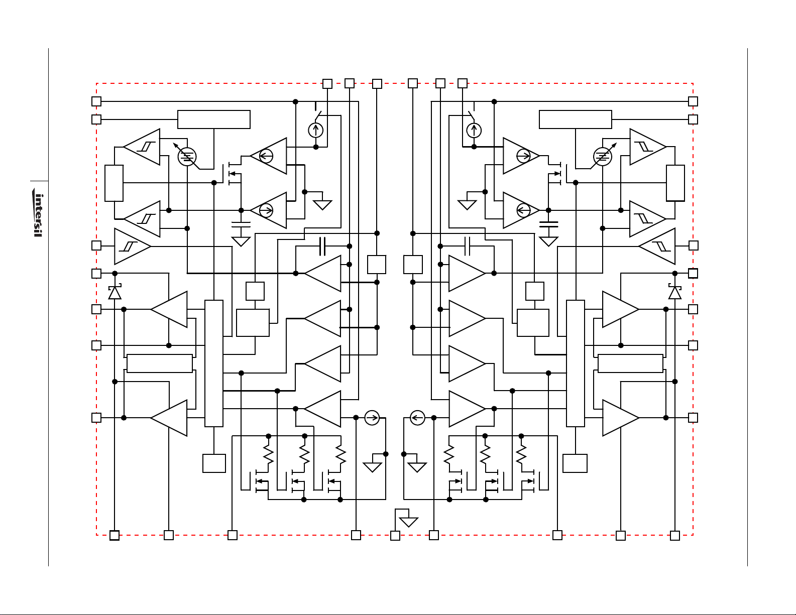
FIGURE 1. SCHEMATIC BLOCK DIAGRAM
Page 3
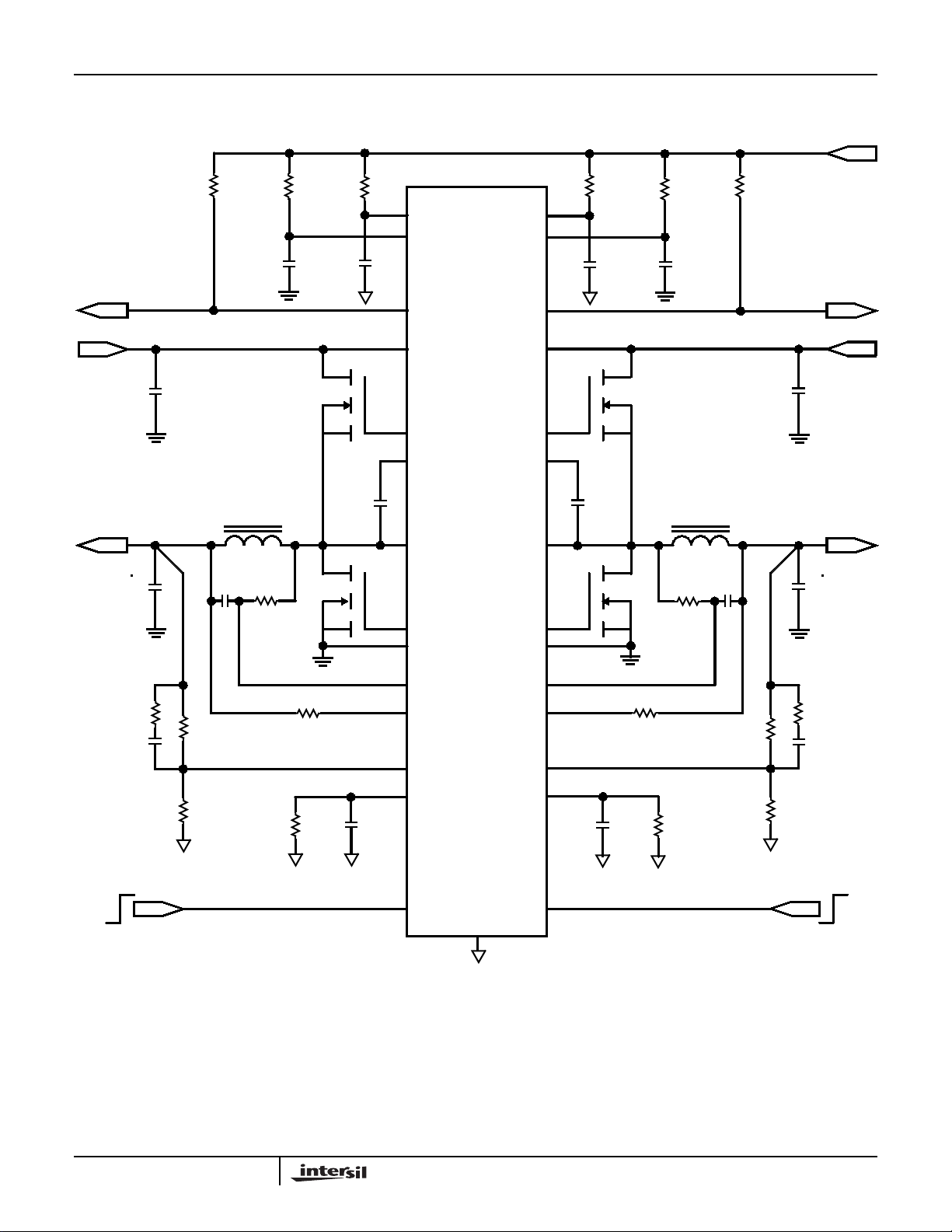
Typical Application
ISL6228
5V
PGOOD2
V
IN2
3.3V TO 25V
C
IN2
V
O2
0.6V TO 5V
C
O2
R
PGOOD2
C
C
SEN2
R
PVCC2
PVCC2
L
O2
R
OCSET2
Q
HIGH_SIDE2
R
VCC2
C
VCC2
C
Q
LOW_SIDE2
BOOT2
VCC2
PVCC2
PGOOD2
VIN2
UGATE2
BOOT2
PHASE2
LGATE2
PGND2
ISL6228
VCC1
PVCC1
PGOOD1
VIN1
UGATE1
BOOT1
PHASE1
LGATE1
PGND1
R
VCC1
C
C
BOOT1
Q
LOW_SIDE1
VCC1
Q
HIGH_SIDE1
R
R
OCSET1
PVCC1
C
PVCC1
L
O1
C
SEN1
R
PGOOD1
PGOOD1
V
IN1
3.3V TO 25V
C
IN1
V
O1
0.6V TO 5V
C
O1
OCSET2
R
FB2
C
FB2
R
TOP2
R
O2
VO2
FB2
R
BOTTOM2
R
FSET2
C
FSET2
FSET2
EN2
OCSET1
VO1
FB1
FSET1
EN1
C
FSET1
R
R
R
BOTTOM1
TOP1
R
O1
R
FSET1
FB1
C
FB1
GND
3
FN9095.2
May 7, 2008
Page 4
ISL6228
Absolute Voltage Ratings Thermal Information
VIN
to GND . . . . . . . . . . . . . . . . . . . . . . . . . . . . . . .-0.3V to +28V
1,2
VCC, PGOOD
to GND . . . . . . . . . . . . . . . . . . . . . -0.3V to +7.0V
1,2
PVCC to GND . . . . . . . . . . . . . . . . . . . . . . . . . . . . . . -0.3V to +7.0V
EN
. . . . . . . . . . . . . . . . . . . . . . . . . . . . -0.3V to GND, VCC +3.3V
1,2
VO
, FB
1,2
PHASE
(<100ns Pulse Width, 10µJ). . . . . . . . . . . . . . . . . . . . . . . . . -5.0V
BOOT
BOOT
UGATE
(<200ns Pulse Width, 20µJ) . . . . . . . . . . . . . . . . . . . . . . . . -4.0V
LGATE
(<100ns Pulse Width, 4µJ). . . . . . . . . . . . . . . . . . . . . . . . . . -2.0V
CAUTION: Do not operate at or near the maximum ratings listed for extended periods of time. Exposure to such conditions may adversely impact product reliability and
result in failures not covered by warranty.
, FSET
1,2
to GND. . . . . . . . . . . . . . . . . . . . . . . (DC) -0.3V to +28V
1,2
to GND. . . . . . . . . . . . . . . . . . . . . . . . . . . . .-0.3V to +33V
1,2
to PHASE
1,2
. . . . . . . . . . . .(DC) -0.3V to PHASE
1,2
. . . . . . . . . . . . . . . . . . . (DC) -0.3V to GND, PVCC +0.3V
1,2
. . . . . . . . . . . . . . -0.3V to GND, VCC +0.3V
1,2
. . . . . . . . . . . . . . . . . . . . . . . . .-0.3V to +7V
1,2
1,2
, BOOT
1,2
+0.3V
NOTES:
is measured in free air with the component mounted on a high effective thermal conductivity test board with “direct attach” features. See
1. θ
JA
Tech Brief TB379.
2. For θ
, the “case temp” location is the center of the exposed metal pad on the package underside.
JC
3. Limits established by characterization and are not production tested.
Thermal Resistance (Typical, Notes 1, 2) θ
(°C/W) θJC (°C/W)
JA
TQFN Package . . . . . . . . . . . . . . . . . . 40 3
Junction Temperature Range. . . . . . . . . . . . . . . . . .-55°C to +150°C
Operating Temperature Range . . . . . . . . . . . . . . . .-40°C to +100°C
Storage Temperature. . . . . . . . . . . . . . . . . . . . . . . .-65°C to +150°C
Pb-free reflow profile . . . . . . . . . . . . . . . . . . . . . . . . . .see link below
http://www.intersil.com/pbfree/Pb-FreeReflow.asp
Recommended Operating Conditions
Ambient Temperature Range. . . . . . . . . . . . . . . . . .-10°C to +100°C
Supply Voltage (VIN to GND) . . . . . . . . . . . . . . . . . . . . 3.3V to 25V
VCC to GND . . . . . . . . . . . . . . . . . . . . . . . . . . . . . . . . . . . . .5V ±5%
PVCC to GND . . . . . . . . . . . . . . . . . . . . . . . . . . . . . . . . . . . .5V ±5%
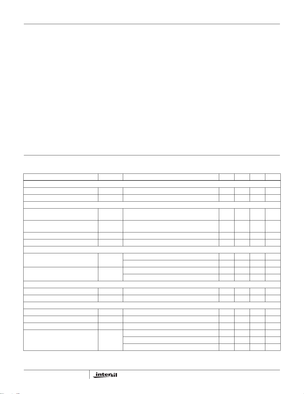
Electrical Specifications These specifications apply for T
PVCC = 5V; Parameters with MIN and/or MAX limits are 100% tested at +25°C, unless otherwise specified.
= -40°C to +100°C; All typical specifications TA = +25°C, VCC = 5V,
A
Temperature limits established by characterization and are not production tested.
PARAMETER SYMBOL TEST CONDITIONS MIN TYP MAX UNIT
VIN
VIN Input Bias Current I
VIN Shutdown Current I
VIN_SHDN
VIN
EN = 5V, VIN = 15V - 16 - µA
EN = GND, VIN = 25V - 0.1 1.0 µA
VCC and PVCC
VCC Input Bias Current in Single-Channel I
VCC Input Bias Current in Dual Channel I
VCC Shutdown Current I
PVCC Shutdown Current I
VCC_SHDNEN1
PVCC_SHDNEN1
VCC_S
VCC_D
EN1 = 5V, FB1 = 0.65V , VIN1 = 3.3V to 25V,
EN
= GND, FB2 = GND, VIN2 = GND
2
EN1 = 5V, FB1 = 0.65V , VIN1 = 3.3V to 25V,
EN
= 5V, FB2 = 0.65V , VIN2 = 3.3V to 25V
2
- 1-
- 2-
= GND, EN2 = GND, VCC = 5V - 0.1 1.0 µA
= GND, EN2 = GND, PVCC = 5V - 0.1 1.0 µA
VCC POR THRESHOLD
Rising VCC POR Threshold Voltage V
Falling VCC POR Threshold Voltage
VCC_THR
V
VCC_THF
= -10°C to +100°C 4.35 4.45 4.55 V
T
A
= -10°C to +100°C 4.10 4.20 4.30 V
T
A
4.33 4.45 4.55 V
4.08 4.20 4.30 V
REGULATION
Reference Voltage V
REF
- 0.6 - V
Regulation Accuracy Close loop -1 - +1 %
PWM
Frequency Range f
SW
Frequency-Set Accuracy f
VO Range V
VO Input Leakage I
VO
VO
= 300kHz -12 - +12 %
SW
0.60 - 5V
EN = 5V, VO = 0.60V - 1 - µA
200 - 600 kHz
EN = 5V, VO = 5V - 7.0 - µA
EN = 0V, VO = 5V - 0.1 - µA
mA
mA
4
FN9095.2
May 7, 2008
Page 5
ISL6228
Electrical Specifications These specifications apply for T
PVCC = 5V; Parameters with MIN and/or MAX limits are 100% tested at +25°C, unless otherwise specified.
= -40°C to +100°C; All typical specifications TA = +25°C, VCC = 5V,
A
Temperature limits established by characterization and are not production tested. (Continued)
PARAMETER SYMBOL TEST CONDITIONS MIN TYP MAX UNIT
ERROR AMPLIFIER
FB Input Bias Current I
FB
FB = 0.60V -33 - 15 nA
FB = 0.60V T
= -10°C to +100°C -35 - 15 nA
A
POWER GOOD
PGOOD Pull-Down Impedance R
PGOOD Leakage Current I
PG_SS
R
PG_SS
R
PG_UV
R
PG_UV
R
PG_OV
R
PG_OV
R
PG_OC
R
PG_OC
PGOOD
PGOOD = 5mA Sink 70 95 125 Ω
PGOOD = 5mA Sink TA = -10°C to +100°C 75 95 125 Ω
PGOOD = 5mA Sink 70 95 125 Ω
PGOOD = 5mA Sink TA = -10°C to +100°C 75 95 125 Ω
PGOOD = 5mA Sink 45 63 85 Ω
PGOOD = 5mA Sink TA = -10°C to +100°C 50 63 85 Ω
PGOOD = 5mA Sink 22 32 45 Ω
PGOOD = 5mA Sink TA = -10°C to +100°C 25 32 45 Ω
PGOOD = 5V - 0.1 1.0 µA
PGOOD Maximum Sink Current (Note 3) - 5.0 - mA
PGOOD Soft-Start Delay t
SS
EN High to PGOOD High 2.20 2.75 3.50 ms
GATE DRIVER
UGATE Pull-Up Resistance (Note 3) R
UGATE Source Current (Note 3) I
UGATE Sink Resistance (Note 3) R
UGATE Sink Current (Note 3) I
LGATE Pull-Up Resistance (Note 3) R
LGATE Source Current (Note 3) I
LGATE Sink Resistance (Note 3) R
LGATE Sink Current (Note 3) I
UGATE to LGATE Deadtime t
LGATE to UGATE Deadtime t
UGPU
UGSRC
UGPD
UGSNK
LGPU
LGSRC
LGPD
LGSNK
UGFLGR
LGFUGR
200mA Source Current - 1.0 1.5 Ω
UGATE - PHASE = 2.5V - 2.0 - A
250mA Sink Current - 1.0 1.5 Ω
UGATE - PHASE = 2.5V - 2.0 - A
250mA Source Current - 1.0 1.5 Ω
LGATE - PGND = 2.5V - 2.0 - A
250mA Sink Current - 0.5 0.9 Ω
LGATE - PGND = 2.5V - 4.0 - A
UGATE falling to LGATE rising, no load - 21 - ns
LGATE falling to UGATE rising, no load - 21 - ns
BOOTSTRAP DIODE
Forward Voltage V
Reverse Leakage I
PVCC = 5V, IF = 2mA - 0.58 - V
F
VR = 25V - 0.2 - µA
R
CONTROL INPUTS
EN High Threshold V
EN Low Threshold V
EN Leakage I
ENTHR
ENTHF
ENL
I
ENH
EN = 0V - 0.1 1.0 µA
EN = 5.0V 1.4 2 2.5 µA
EN = 5.0V T
= -10°C to +100°C 1.5 2 2.5 µA
A
2.0 --V
--1.0 V
PROTECTION
OCSET-VO Threshold V
OCSET 10µA Current Source I
OCSETTHR
OCSET
EN = 5V 8.8 10 10.5 µA
EN = 5V T
= -10°C to +100°C 9 10 10.5 µA
A
-1.75 0 1.75 mV
EN = 0V - 0 - µA
OCSET 10µA Current Source Impedance R
OCSETIMP
UVP Threshold V
OVP Rising Threshold V
OVP Falling Threshold V
OVR
OVF
EN = 5V, OCSET = 1.2V - 600 - kΩ
UV
81 86 87 %
113 116 120 %
100 102 106 %
5
FN9095.2
May 7, 2008
Page 6

ISL6228
Electrical Specifications These specifications apply for T
PVCC = 5V; Parameters with MIN and/or MAX limits are 100% tested at +25°C, unless otherwise specified.
Temperature limits established by characterization and are not production tested. (Continued)
PARAMETER SYMBOL TEST CONDITIONS MIN TYP MAX UNIT
OTP Rising Threshold (Note 3) T
OTP Hysteresis (Note 3) T
OTR
OTHYS
Functional Pin Descriptions
GND (Bottom Pad)
Signal common of the IC. Unless otherwise stated, signals
are referenced to the GND pin.
FSET2 (Pin 1)
The FSET2 pin programs the PWM switching frequency of
Channel 2. Program the desired PWM frequency with a
resistor and a capacitor connected across the FSET2 and
GND pins.
VIN2 (Pin 2)
The VIN2 pin measures the input voltage of the Channel 2
converter. It is a required input to the Channel 2 R
modulator. Connect the VIN2 pin to the drain of the
Channel 2 high-side MOSFET.
VCC2 (Pin 3)
The VCC2 pin is the input bias voltage for Channel 2.
Connect +5V to the VCC2 pin. Decouple with at least 1µF of
a MLCC capacitor from the VCC2 pin to the GND pin.
VCC1 (Pin 4)
The VCC1 pin is the input bias voltage for Channel 1.
Connect +5V to the VCC1 pin. Decouple with at least 1µF of
a MLCC capacitor from the VCC1 pin to the GND pin.
VIN1 (Pin 5)
The VIN1 pin measures the input voltage of the Channel 1
converter. It is a required input to the Channel 1 R
modulator. Connect the VIN1 pin to the drain of the
Channel 1 high-side MOSFET.
FSET1 (Pin 6)
The FSET1 pin programs the PWM switching frequency of
Channel 1. Program the desired PWM frequency with a
resistor and a capacitor connected across the FSET1 and
GND pins.
PGOOD1 (Pin 7)
The PGOOD1 pin is an open-drain output that indicates
when the Channel 1 converter is able to supply regulated
voltage. Connect the PGOOD1 pin to +5V through a pull-up
resistor.
FB1 (Pin 8)
The FB1 pin is the inverting input of the control-loop error
amplifier for Channel 1. The Channel 1 converter output
voltage regulates to 600mV from the FB1 pin to the GND pin.
Program the desired output voltage with a resistor network
3
PWM
3
PWM
= -40°C to +100°C; All typical specifications TA = +25°C, VCC = 5V,
A
- 150 - °C
- 25 - °C
connected across the VO1, FB1, and GND pins. Select the
resistor values such that FB1 to GND is 600mV when the
converter output voltage is at the programmed regulation
value.
VO1 (Pin 9)
The VO1 pin measures the Channel 1 converter output
voltage and is used as an input to the Channel 1 R
modulator. It also serves as part of Channel 1 inductor
current sensing and the OCP overcurrent fault protection
circuit.
OCSET1 (Pin 10)
The OCSET1 pin measures the Channel 1 inductor current
and programs the threshold of the OCP overcurrent fault
protection.
EN1 (Pin 11)
The EN1 pin is the on/off switch of Channel 1. The soft-start
sequence begins when the EN1 pin is pulled above the
rising threshold voltage V
power-on reset (POR) rising threshold voltage
and VCC1 is above the
ENTHR
V
VCC_THR
When the EN1 pin is pulled below the falling threshold
voltage V
PWM1 immediately stops.
ENTHF
PHASE1 (Pin 12)
The PHASE1 pin is the current return path for the Channel 1
high-side MOSFET gate driver. Connect the PHASE1 pin to
the node consisting of the high-side MOSFET source, the
low-side MOSFET drain, and the output inductor of the
Channel 1 converter.
UGATE1 (Pin 13)
The UGATE1 pin is the output of the Channel 1 high-side
MOSFET gate driver. Connect the UGATE1 pin to the gate
of the Channel 1 converter high-side MOSFET.
BOOT1 (Pin 14)
The BOOT1 pin stores the input voltage for the Channel 1
high-side MOSFET gate driver. Connect an MLCC capacitor
across the BOOT1 and PHASE1 pins. The boot capacitor is
charged through an internal boot diode connected from the
PVCC1 pin to the BOOT1 pin, each time the PHASE1 pin
drops below PVCC1 minus the voltage dropped across the
internal boot diode.
PVCC1 (Pin 15)
The PVCC1 pin is the input voltage bias for the Channel 1
low-side MOSFET gate drivers. Connect +5V to the PVCC1
3
PWM
.
6
FN9095.2
May 7, 2008
Page 7

ISL6228
pin. Decouple with at least 1µF of an MLCC capacitor across
the PVCC1 and PGND1 pin.
LGATE1 (Pin 16)
The LGATE1 pin is the output of the Channel 1 converter
low-side MOSFET gate driver. Connect the LGATE1 pin to
the gate of the Channel 1 converter low-side MOSFET.
PGND1 (Pin 17)
The PGND1 pin is the current return path for the Channel 1
converter low-side MOSFET gate driver. Connect the
PGND1 pin to the source of the Channel 1 converter lowside MOSFET through a low impedance path, preferably in
parallel with the trace connecting the LGATE1 pin to the gate
of the Channel 1 converter low-side MOSFET.
PGND2 (Pin 18)
The PGND2 pin is the current return path for the Channel 2
converter low-side MOSFET gate driver. Connect the
PGND2 pin to the source of the Channel 2 converter lowside MOSFET through a low impedance path, preferably in
parallel with the trace connecting the LGATE2 pin to the gate
of the Channel 2 converter low-side MOSFET.
LGATE2 (Pin 19)
The LGATE2 pin is the output of the Channel 2 converter
low-side MOSFET gate driver. Connect to the gate of the
Channel 2 converter low-side MOSFET.
PVCC2 (Pin 20)
The PVCC2 pin is the input voltage bias for the Channel 2
low-side MOSFET gate drivers. Connect +5V to the PVCC2
pin. Decouple with at least 1µF of an MLCC capacitor across
the PVCC2 and PGND2 pin.
BOOT2 (Pin 21)
The BOOT2 pin stores the input voltage for the Channel 2
high-side MOSFET gate driver. Connect an MLCC capaci tor
across the BOOT2 and PHASE2 pins. The boot capacitor is
charged through an internal boot diode connected from the
PVCC2 pin to the BOOT2 pin, each time the PHASE2 pin
drops below PVCC2 minus the voltage dropped across the
internal boot diode.
UGATE2 (Pin 22)
The UGATE2 pin is the output of the Channel 2 high-side
MOSFET gate driver. Connect to the gate of the Channel 2
converter high-side MOSFET.
PHASE2 (Pin 23)
The PHASE2 pin is the current return path for the Channel 2
high-side MOSFET gate driver. Connect the PHASE2 pin to
the node consisting of the high-side MOSFET source, the
low-side MOSFET drain, and the output inductor of the
Channel 2 converter.
EN2 (Pin 24)
The EN2 pin is the on/off switch of Channel 2. The soft-start
sequence begins when the EN2 pin is pulled above the
rising threshold voltage V
power-on reset (POR) rising threshold voltage
When the EN2 pin is pulled below the falling threshold
voltage V
, PWM2 immediately stops.
ENTHF
and VCC2 is above the
ENTHR
V
VCC_THR
.
OCSET2 (Pin 25)
The OCSET2 pin measures the Channel 2 inductor current
and programs the threshold of the OCP overcurrent fault
protection.
VO2 (Pin 26)
The VO2 pin measures the Channel 2 converter output
voltage and is used as an input to the Channel 2 R
modulator. It also serves as part of Channel 2 inductor
current sensing and the OCP overcurrent fault protection
circuit.
3
PWM
FB2 (Pin 27)
The FB2 pin is the inverting input of the control-loop error
amplifier for Channel 2. The Channel 2 converter output
voltage regulates to 600mV from the FB2 pin to the GND pin.
Program the desired output voltage with a resistor network
connected across the VO2, FB2, and GND pins. Select the
resistor values such that FB2 to GND is 600mV when the
converter output voltage is at the programmed regulation
value.
PGOOD2 (Pin 28)
The PGOOD2 pin is an open-drain output that indicates
when the Channel 2 converter is able to supply regulated
voltage. Connect the PGOOD2 pin to +5V through a pull-up
resistor.
Theory of Operation
Two Separate Channels
The ISL6228 is a dual channel controller. Pins 4~17 are
dedicated to Channel 1, and pins 1~3 and pins 18~28 are
dedicated to Channel 2. The two channels are identical and
almost entirely independent, with the exception of sharing
the GND pin. Unless otherwise stated, only an individual
channel is discussed, and the conclu sion applies to both
channels.
Modulator
The ISL6228 modulator features Intersil’s R3 technology, a
hybrid of fixed frequency PWM control and variable
frequency hysteretic control. Intersil’s R
simultaneously affect the PWM switching frequency and
PWM duty cycle in response to input voltage and output load
transients. The R
which is an analog representation of the output inductor
ripple current. The duty-cycle of V
and discharge current through a ripple capacitor C
3
modulator synthesizes an AC signal VR,
3
technology can
is the result of charge
R
. The
R
7
FN9095.2
May 7, 2008
Page 8
ISL6228
current through CR is provided by a transconductance
amplifier g
The positive slope of V
V
RPOS
The negative slope of V
V
RNEGgmVOUTCR
Where g
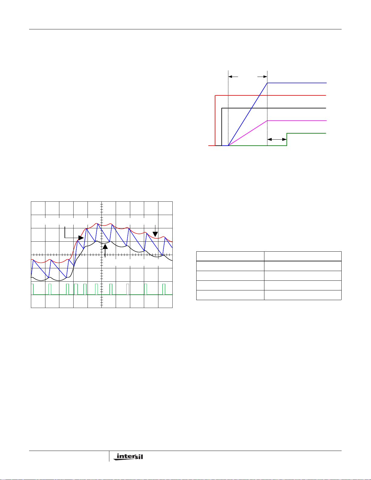
A window voltage V
amplifier output voltage V
which the ripple voltage V
V
is set by a resistor connected across the FSET and GND
W
pins. The V
comparator in which V
and V
PWM pulses being generated as V
V
COMP
that measures the VIN and VO pin voltages.
m
gm()VINV
is the gain of the transconductance amplifier.
m
R, VCOMP,
is the higher threshold voltage. Figure 2 shows
W
can be written as Equation 1:
R
–()CR⁄⋅=
OUT
can be written as Equation 2:
R
⁄⋅=
is referenced with respect to the error
W
, creating an envelope into
COMP
is compared. The amplitude of
R
and VW signals feed into a window
is the lower threshold voltage
COMP
traverses the VW and
R
thresholds. The PWM switching frequency is
(EQ. 1)
(EQ. 2)
proportional to the slew rates of the positive and negative
slopes of V
between V
Ripple Capacitor Voltage C
it is inversely proportional to the voltage
R;
and V
W
COMP.
R
Window Voltage V
W
Soft-Start Delay tSS begins and the output voltage begins to
rise. The FB pin ramps to 0.6V in approximately 1.5ms and
the PGOOD pin goes to high impedance approximately
1.25ms after the FB pin voltage reaches 0.6V.
1.5ms
1.25ms
FIGURE 3. SOFT-START SEQUENCE
Vo
VCC and PVCC
EN
FB
PGOOD
The PGOOD pin indicates when the converter is capable of
supplying regulated voltage. The PGOOD pin is an
undefined impedance if V
threshold V
V
. The ISL6228 features a unique fault-identification
CCF
, or if VCC is below the falling POR threshold
CCR
has not reached the rising POR
CC
capability that can drastically reduce trouble-shooting time
and effort. The pull-down resistance of the PGOOD pin
corresponds to the fault st atus of the controller . The PGOOD
pull-down resistance is 95Ω during soft-start or if an UVP
occurs, 30Ω for an OCP, or 60Ω for OVP.
Error Amplifier Voltage V
PWM
FIGURE 2. MODULATOR W AVEFORMS DURING LOAD
TRANSIENT
COMP
Power-On Reset
The ISL6228 is disabled until the voltage at the VCC pin has
increased above the rising power-on reset (POR) V
CCR
threshold voltage. The controller will be disabled when the
voltage at the VCC pin decreases below the falling POR
V
threshold voltage.
CCF
EN, Soft-Start and PGOOD
The ISL6228 uses a digital soft-start circuit to ramp the
output voltage of the converter to the programmed regulation
setpoint at a predictable slew rate. The slew rate of the
soft-start sequence has been selected to limit the in-rush
current through the output capacitors as they charge to the
desired regulation voltage. When the EN pin is pulled above
the rising EN threshold voltage V
ENTHR
, the PGOOD
TABLE 1. PGOOD PULL-DOWN RESISTANCE
CONDITION PGOOD RESISTANCE
VCC Below POR Undefined
Soft-start or Undervoltage 90Ω
Overvoltage 60Ω
Overcurrent 30Ω
MOSFET Gate-Drive Outputs LGATE and UGATE
The ISL6228 has internal gate-drivers for the high-side and
low-side N-Channel MOSFETs. The low-side gate-drivers
are optimized for low duty-cycle applications where the lowside MOSFET conduction losses are dominant, requiring a
low r
DS(ON)
small in order to clamp the gate of the MOSFET below the
V
GS(th)
turn-off can be considerable because the gate charge of a
low r
DS(ON)
protection prevents a gate-driver output from turning on until
the opposite gate-driver output has fallen below
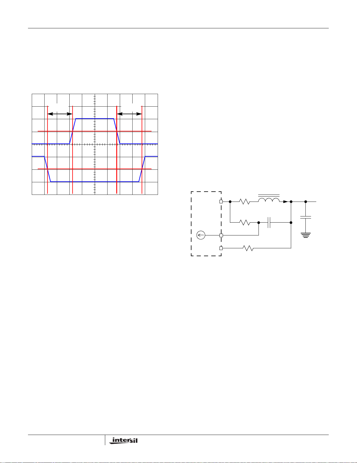
approximately 1V. The dead-time shown in Figure 4 is
extended by the additional period that the falling gate voltage
stays above the 1V threshold. The typical dead-time is 21ns.
The high-side gate-driver output voltage is measured across
the UGATE and PHASE pins while the low-side gate-driver
output voltage is measured across the LGATE and PGND
MOSFET. The LGATE pull-down resistance is
at turnoff. The current transient through the gate at
MOSFET can be large. Adaptive shoot-through
8
FN9095.2
May 7, 2008
Page 9
ISL6228
pins. The power for the LGATE gate-driver is sourced
directly from the PVCC pin. The power for the UGATE gatedriver is sourced from a “boot” capacitor connected across
the BOOT and PHASE pins. The boot capacitor is charged
from a 5V bias supply through a “boot diode” each time the
low-side MOSFET turns on, pulling the PHASE pin low. The
ISL6228 has an integrated boot diode connected from the
PVCC pin to the BOOT pin.
t
LGFUGR
50%
UGATE
LGATE
50%
FIGURE 4. LGATE AND UGATE DEAD-TIME
t
UGFLGR
Diode Emulation
The ISL6228 implements forced continuous-conductionmode (CCM) at heavy load and diode-emulation-mode
(DEM) at light load, to optimize efficiency in the entire load
range. The transition is automatically achieved by detecting
the output load current.
Positive-going inductor current flows from either the source
of the high-side MOSFET, or the drain of the low-side
MOSFET. Negative-going inductor current flows into the
drain of the low-side MOSFET. When the low-side MOSFET
conducts positive inductor current, the phase voltage will be
negative with respect to the GND and PGND pins.
Conversely, when the low-side MOSFET conducts negative
inductor current, the phase voltage will be positive with
respect to the GND and PGND pins. The ISL6228 monitors
the phase voltage, when the low-side MOSFET is
conducting inductor current, to determine the direction of the
inductor current.
When the output load current is greater than or equal to ½
the inductor ripple current, the inductor current is always
positive, and the converter is always in CCM. The ISL6228
minimizes the conduction loss in this condition by forcing the
low-side MOSFET to operate as a synchronous rectifier.
When the output load current is less than ½ the inductor
ripple current, negative inductor current occurs. Sinking
negative inductor through the low-side MOSFET lowers
efficiency through unnecessary conduction losses. The
ISL6228 automatically enters DEM after the PHASE pin has
detected positive voltage and LGATE was allowed to go high
for eight consecutive PWM switching cycles. The ISL6228
will turn off the low-side MOSFET once the phase voltage
turns positive, indicating negative inductor current. The
ISL6228 will return to CCM on the following cycle after the
PHASE pin detects negative voltage, indicating that the body
diode of the low-side MOSFET is conducting positive
inductor current.
Efficiency can be further improved with a reduction of
unnecessary switching losses by reducing the PWM
frequency. It is characteristic of the R
3
architecture for the
PWM frequency to decrease while in diode emulation. The
extent of the frequency reduction is proportional to the
reduction of load current. Upon entering DEM, the PWM
frequency makes an initial step-reduction because of a 33%
step-increase of the window voltage V
.
W
Overcurrent Protection
The overcurrent protection (OCP) setpoint is programmed
with resistor R
and PHASE pins.
PHASE
ISL6228
10µA
OCSET
VO
FIGURE 5. OVERCURRENT-SET CIRCUIT
Figure 5 shows the overcurrent-set circuit. The inductor
consists of inductance L and the DC resistance DCR. The
inductor DC current I
given by Equation 3:
V
DCRIL
DCR•=
The ISL6228 sinks 10µA current into the OCSET pin,
creating a DC voltage drop across the resistor R
given by Equation 4:
V
ROCSET
10μ AR
Resistor RO is connected between the VO pin and the actual
output voltage of the converter. During normal operation, the
VO pin is a high impedance path, therefore there is no
voltage drop across R
the OCSET pin and the VO pin can be established using
Equation 5:
V
OCSETV–VOVDCRV–ROCSETIL
that is connected across the OCSET
OCSET
DCR
+
R
OCSET
V
ROCSET
+
R
O
creates a voltage drop across DCR,
L
•=
OCSET
. The DC voltage difference between
O
L
I
L
V
DCR
C
SEN
_
_
DCR• 10μ AR
V
O
OCSET
•–==
OCSET
C
O
(EQ. 3)
,
(EQ. 4)
(EQ. 5)
9
FN9095.2
May 7, 2008
Page 10

ISL6228
The ISL6228 monitors the OCSET pin and the VO pin
voltages. Once the OCSET pin voltage is higher than the VO
pin voltage for more than 10µs, the ISL6228 declares an OCP
fault. The value of R
IOCDCR•
R
OCSET
---------------------------
=
10μ A
is then written as Equation 6:
OCSET
(EQ. 6)
Where:
-R
(Ω) is the resistor used to program the
OCSET
overcurrent setpoint
is the output current threshold that will activate the
-I
OC
OCP circuit
- DCR is the inductor DC resistance
For example, if I
R
Resistor R
OCSET
is R
OCSET
is 20A and DCR is 4.5mΩ, the choice of
OC
OCSET
= 20A x 4.5mΩ/10µA = 9kΩ.
and capacitor C
form an R-C network
SEN
to sense the inductor current. To sense the inductor current
correctly not only in DC operation, but also during dynamic
operation, the R-C network time constant R
OCSETCSEN
needs to match the inductor time constant L/DCR. The value
of C
C
For example, if L is 1.5µH, DCR is 4.5mΩ, and R
9kΩ, the choice of C
Upon converter startup, capacitor C
is then written as Equation 7:
SEN
L
-----------------------------------------
=
SEN
R
OCSET
DCR•
SEN
(EQ. 7)
is
OCSET
= 1.5µH/(9kΩ x 4.5mΩ) = 0.037µF.
initial voltage is 0V.
SEN
To prevent false OCP, a 10µA current source flows out of the
VO pin during start up, generating a voltage drop on resistor
R
, which has the same resistance as R
O
OCSET
. When
PGOOD pin goes high, the VO pin current source will
terminate.
When an OCP fault is declared, the PGOOD pin will pull
down to 30Ω
and latch off the converter . The fault will remain
latched until the EN pin has been pulled below the falling EN
threshold voltage V
falling POR threshold voltage
or if VCC has decayed below the
ENTHF
V
VCC_THF
.
Overvoltage Protection
The OVP fault detection circuit triggers after the FB pin voltage
is above the rising overvoltage threshold V
2µs. The FB pin voltage is 0.6V in normal operation. The rising
overvoltage threshold V
is typically 116%. That means if
OVR
the FB pin voltage is above 1 16%x 0.6V = 0.696V, for more
than 2µs, an OVP fault is declared.
When an OVP fault is declared, the PGOOD pin will pull
down to 60Ω
and latch-off the converter. The OVP fault will
remain latched until the EN pin has been pulled below the
falling EN threshold voltage V
or if VCC has decayed
ENTHF
below the falling POR threshold voltage
Although the converter has latched-off in response to an
OVP fault, the LGAT E gate-driver output will retain the ability
to toggle the low-side MOSFET on and off, in response to
for more than
OVR
V
VCC_THF
.
the output voltage transversing the V
OVR
and V
OVF
thresholds. The LGATE gate-driver will turn on the low-side
MOSFET to discharge the output voltage, protecting the
load. The LGATE gate-driver will turn off the low-side
MOSFET once the FB pin voltage is lower than the falling
overvoltage threshold V
overvoltage threshold V
for more than 2µs. The falling
OVF
is typically 106%. That means if
OVF
the FB pin voltage falls below 106% x 0.6V = 0.636V, for
more than 2µs, the LGATE gate-driver will turn off the lowside MOSFET. If the output voltage rises again, the LGATE
driver will again turn on the low-side MOSFET when the FB
pin voltage is above the rising overvoltage threshold V
OVR
for more than 2µs. By doing so, the ISL6228 protects the
load when there is a consistent overvoltage condition.
Undervoltage Protection
The UVP fault detection circuit triggers after the FB pin
voltage is below the undervoltage threshold V
for more
UV
than 2µs. The FB pin voltage is 0.6V in normal operation.
The undervoltage threshold V
is typically 86%. That
UV
means if the FB pin voltage is below 86% x 0.6V = 0.516V,
for more than 2µs, an UVP fault is declared, and the
PGOOD pin will pull down to 95Ω
and latch-off the converter.
The fault will remain latched until the EN pin has been pulled
below the falling EN threshold voltage V
ENTHF
or if VCC has
decayed below the falling POR threshold voltage
V
VCC_THF.
Programming the Output Voltage
When the converter is in regulation there will be 0.6V from
the FB pin to the GND pin. Connect a two-resistor voltage
divider across the VO pin and the GND pin with the output
node connected to the FB pin. Scale the voltage-divider
network such that the FB pin is 0.6V with respect to the GND
pin when the converter is regulating at the desired output
voltage. The output voltage can be programmed from 0.6V
to 5V.
Programming the output volt a ge is written as Equation 8:
R
V
REFVO
BOTTOM
•=
---------------------------------------------------
R
+
TOPRBOTTOM
Where:
-V
is the desired output voltage of the converter
O
- The voltage to which the converter regulates the FB pin
is the V
-R
REF
is the voltage-programming resistor that connects
TOP
from the FB pin to the converter output. In addition to
setting the output voltage, this resistor is part of the loop
compensation network
-R
BOTTOM
is the voltage-programming resistor that
connects from the FB pin to the GND pin
Choose R
value first, and calculate R
TOP
BOTTOM
to Equation 9:
V
R•
REF
R
BOTTOM
-----------------------------------
=
VOV
–
TOP
REF
(EQ. 8)
according
(EQ. 9)
10
FN9095.2
May 7, 2008
Page 11
ISL6228
Programming the PWM Switching Frequency
The ISL6228 does not use a clock signal to produce PWMs.
The PWM switching frequency f
resistor R
that is connected from the FSET pin to the
FSET
is programmed by the
SW
GND pin. The approximate PWM switching frequency is
written as Equation 10:
SW
⋅
KR
FSET
1
---------------------------
f
=
Estimating the value of R
1
=
------------------
•
Kf
SW
R
FSET
is written as Equation 11:
FSET
(EQ. 10)
(EQ. 11)
Where:
is the PWM switching frequency
-f
SW
-R
- K = 1.5 x 10
is the fSW programming resistor
FSET
-10
It is recommended that whenever the control loop
compensation network is modified, f
for the correct frequency and if necessary, adjust R
should be checked
SW
FSET
.
Compensation Design
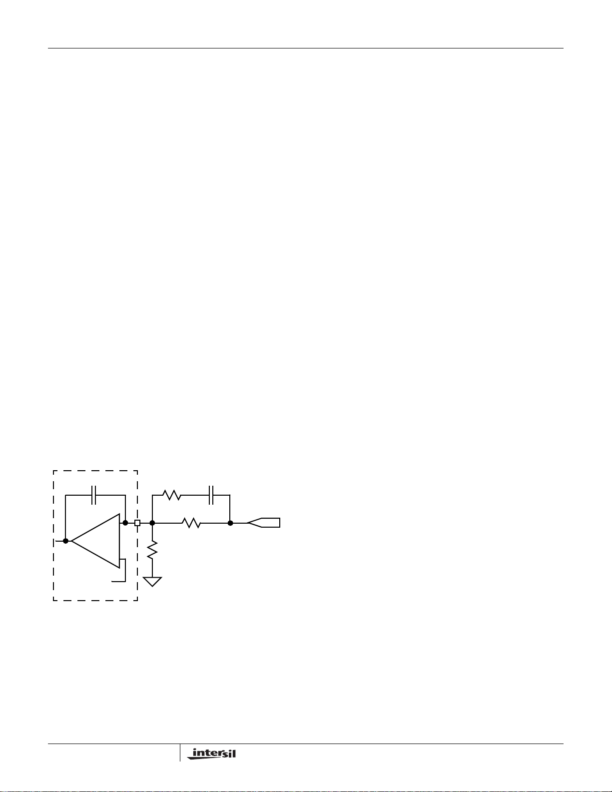
Figure 6 shows the recommended Type-II compensation
circuit. The FB pin is the inverting input of the error amplifier.
The COMP signal, the output of the error amplifier, is inside the
chip and unavailable to users. C
integrated inside the IC, connec ting across the FB pi n and the
COMP signal. R
, RFB, CFB and C
TOP
compensator. The frequency domain transfer function is given
by Equation 12:
1sR
•+
G
COMP
-------------------------------------------------------------------------------------------
s()
=
sR
TOPCINT
C
= 100pF
INT
TOPRFB
is a 100pF capacitor
INT
form the Type-II
INT
+()C•
1sRFBC•
R
FB
FB
•+()•••
FB
C
FB
(EQ. 12)
General Application Design Guide
This design guide is intended to provide a high-level
explanation of the steps necessary to design a single-phase
power converter. It is assumed that the reader is famil iar with
many of the basic skills and techniques referenced in the
following section. In addition to this guide, Intersil provides
complete reference designs that include schematics, bills of
materials, and example board layouts.
Selecting the LC Output Filter
The duty cycle of an ideal buck converter is a function of the
input and the output voltage. This relationship is written as
Equation 13:
V
O
---------
D
=
V
IN
The output inductor peak-to-peak ripple current is written as
Equation 14:
VO1D–()•
------------------------------
I
=
PP
fSWL•
A typical step-down DC/DC converter will have an I
20% to 40% of the maximum DC output load current. The
value of I
is selected based upon several criteria such as
PP
MOSFET switching loss, inductor core loss, and the resistive
loss of the inductor winding. The DC copper loss of the
inductor can be estimated by Equation 15:
2
P
COPPERILOAD
Where I
LOAD
DCR•=
is the converter output DC current.
The copper loss can be significant so attention has to be
given to the DCR selection. Another factor to consider when
choosing the inductor is its saturation characteristics at
elevated temperature. A saturated inductor could cause
destruction of circuit components, as well as nuisance OCP
faults.
(EQ. 13)
(EQ. 14)
of
P-P
(EQ. 15)
R
TOP
-
FB
COMP
EA
+
REF
ISL6228
FIGURE 6. COMPENSATION REFERENCE CIRCUIT
R
BOTTOM
VO
The LC output filter has a double pole at its resonant frequency
that causes rapid phase change. The R
3
modulator used in the
ISL6228 makes the LC output filter resemble a first order
system in which the closed loop stability can be achieved with
the recommended Type-II compensation network. Intersil
provides a PC-based tool (example page is shown later) that
can be used to calculate compensation network component
values and help simulate the loop frequency response.
11
A DC/DC buck regulator must have output capacitance C
into which ripple current I
a corresponding ripple voltage V
can flow. Cu rre nt IPP develops
P-P
across C
P-P
which is the
O,
O
sum of the voltage drop across the capacitor ESR and of the
voltage change stemming from charge moved in and out of
the capacitor. These two voltages are written as
Equation 16:
ΔV
ESRIP-P
E• SR=
(EQ. 16)
and Equation 17:
ΔV
=
C
P-P
-----------------------------
8COf•
•
SW
(EQ. 17)
I
If the output of the converter has to support a load with high
pulsating current, several capacitors will need to be p aralleled
to reduce the total ESR until the required V
is achieved.
P-P
The inductance of the capacitor can cause a brief voltage dip
if the load transient has an extremely high slew rate. Low
inductance capacitors sh ould be co nsider ed. A cap a citor
FN9095.2
May 7, 2008
Page 12
ISL6228
dissipates heat as a function of RMS current and frequency.
Be sure that I
is shared by a sufficient quantity of paralleled
P-P
capacitors so that they operate below the maximum rated
RMS current at f
. Take into account that the rated value of
SW
a capacitor can fade as much as 50% as the DC voltage
across it increases.
Selection of the Input Capacitor
The important parameters for the bulk input capacitance are
the voltage rating and the RMS current rating. For reliable
operation, select bulk capacitors with voltage and current
ratings above the maximum input voltage and capable of
supplying the RMS current required by the switching circuit.
Their voltage rating should be at least 1.25 times greater
than the maximum input voltage, while a voltage rating of 1.5
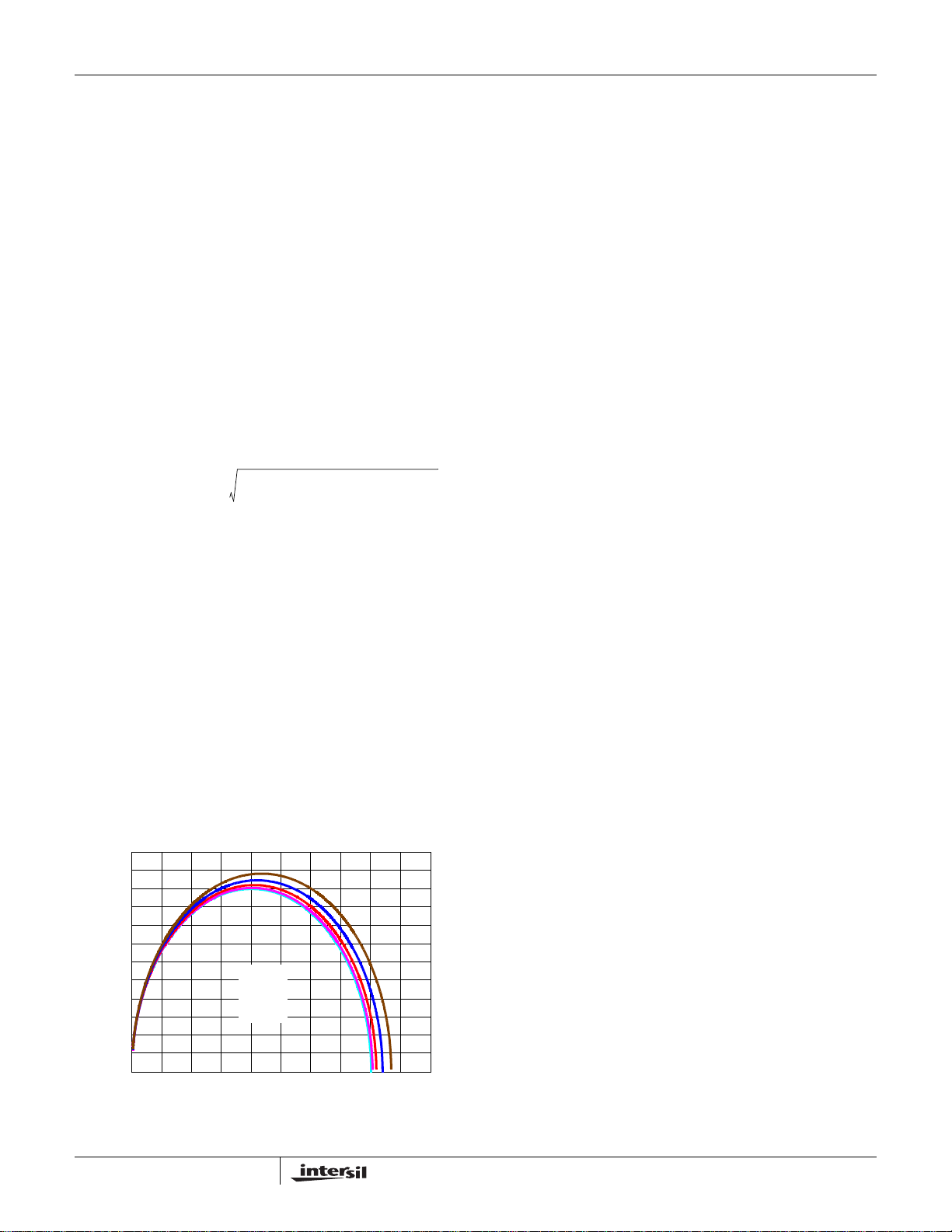
times is a preferred rating. Figure 7 is a graph of the input
RMS ripple current, normalized relative to output loa d current,
as a function of duty cycle that is adjusted for converter
efficiency. The ripple current calculation is written as
Equation 18:
I
IN_RMS NORMALIZED,
2
I
MAX
-----------------------------------------------------------------------------------------------------
=
2
DD
–()⋅()xI
+
I
MAX
⎛⎞
⎝⎠
Where:
-I
is the maximum continuous I
MAX
of the converter
LOAD
- x is a multiplier (0 to 1) corresponding to the inductor
peak-to-peak ripple amplitude expressed as a
percentage of I
(0% to 100%)
MAX
- D is the duty cycle that is adjusted to take into account
the efficiency of the converter which is written as:
V
O
--------------------------
D
=
VINEFF⋅
In addition to the bulk capacitance, some low ESL ceramic
capacitance is recommended to decouple between the drain
of the high-side MOSFET and the source of the low-side
MOSFET.
0.60
0.55
0.50
0.45
0.40
0.35
0.30
0.25
0.20
0.15
0.10
0.05
NORMALIZED INPUT RMS RIPPLE CURRENT
0
0 0.1 0.2 0.3 0.4 0.5 0.6 0.7 0.8 0.9 1.0
FIGURE 7. NORMALIZED RMS INPUT CURRENT
x = 1
x = 0.75
x = 0.50
x = 0.25
x = 0
DUTY CYCLE
2
D
MAX
------
12
(EQ. 18)
(EQ. 19)
⋅⋅
MOSFET Selection and Considerations
Typically, a MOSFET cannot tolerate even brief excursions
beyond their maximum drain to source voltage rating. The
MOSFETs used in the power stage of the converter should
have a maximum V
rating that exceeds the sum of the
DS
upper voltage tolerance of the input power source and the
voltage spike that occurs when the MOSFET switches off.
There are several power MOSFET s readily available that are
optimized for DC/DC converter applications. The preferred
high-side MOSFET emphasizes low gate charge so that the
device spends the least amount of time dissipating power in
the linear region. Unlike the low-side MOSFET which has the
drain-source voltage clamped by its body diode during turn
off, the high-side MOSFET turns off with V
IN-VOUT
, plus the
spike, across it. The preferred low-side MOSFET
emphasizes low r
DS(ON)
when fully saturated to minimize
conduction loss.
For the low-side (LS) MOSFET, the power loss can be
assumed to be conductive only and is written as Equation 20:
P
CON_LSILOAD
2
r⋅
DS ON()_LS
1D–()•≈
(EQ. 20)
For the high-side (HS) MOSFET, the its conduction loss is
written as Equation 21:
P
CON_HSILOAD
2
r•
DS ON()_HS
D•=
(EQ. 21)
For the high-side MOSFET, the switching loss is written as
Equation 22:
P
SW_HS
VINI
VALLEYtON
---------------------------------------------------------------- -
2
f•
••
V
INIPEAKtOFF
SW
-------------------------------------------------------------
+=
f•
••
2
SW
(EQ. 22)
Where:
-I
is the difference of the DC component of the
VALLEY
inductor current minus 1/2 of the inductor ri pp l e current
-I
is the sum of the DC component of the inductor
PEAK
current plus 1/2 of the inductor ripple current
is the time required to drive the device into
-t
ON
saturation
is the time required to drive the device into cut-off
-t
OFF
Selecting The Bootstrap Capacitor
The selection of the bootstrap capacitor is written as
Equation 23:
Q
BOOT
=
ΔV
BOOT
C
g
------------------------
Where:
is the total gate charge required to turn on the
-Q
g
high-side MOSFET
- ΔV
, is the maximum allowed voltage decay across
BOOT
the boot capacitor each time the high-side MOSFET is
switched on
(EQ. 23)
12
FN9095.2
May 7, 2008
Page 13
ISL6228
As an example, suppose the high-side MOSFET has a total
gate charge Q
, of 25nC at VGS= 5V, and a ΔV
g
BOOT
of
200mV . The calculated bootstrap capacitance is 0.125µF; for
a comfortable margin, select a capacitor that is double the
calculated capacitance. In this example, 0.22µF will suffice.
Use an X7R or X5R ceramic capacitor.
Layout Considerations
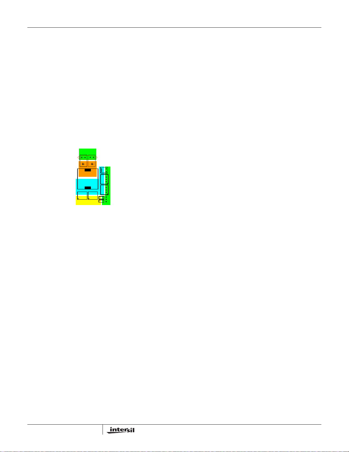
As a general rule, power should be on the bottom layer of
the PCB and weak analog or logic signals are on the top
layer of the PCB. The ground-plane layer should be adjacent
to the top layer to provide shielding. The ground plane layer
should have an island located under the IC, the
compensation components, and the FSET components. The
island should be connected to the rest of the ground plane
layer at one point.
VIAS TO
GROUND
PLANE
INDUCTOR
HIGH-SIDE
MOSFETS
FIGURE 8. TYPICAL POWER COMPONENT PLACEMENT
GND
VOUT
PHASE
NODE
VIN
OUTPUT
CAPACITORS
SCHOTTKY
DIODE
LOW-SIDE
MOSFETS
INPUT
CAPACITORS
Signal Ground and Power Ground
The bottom of the ISL6228 TQFN package is the signal
ground (GND) terminal for analog and logic signals of the IC.
Connect the GND pad of the ISL6228 to the island of ground
plane under the top layer using several vias, for a robust
thermal and electrical conduction path. Connect the input
capacitors, the output capacitors, and the source of the
lower MOSFETs to the power ground plane.
PGND (Pins 17 and 18)
This is the return path for the pull-dow n of th e LGATE
low-side MOSFET gate driver. Ideally, PGND should be
connected to the source of the low-side MOSFET with a
low-resistance, low-inductance path.
VIN (Pins 2 and 5)
The VIN pin should be connected close to the drain of the
high-side MOSFET, using a low resistance and low
inductance path.
VCC (Pins 3 and 4)
For best performance, place the decoupling capacitor very
close to the VCC and GND pins.
EN (Pins 11 and 24), and PGOOD (Pins 7 and 28)
These are logic signals that are referenced to the GND pin.
Treat as a typical logic signal.
OCSET (Pins 10 and 25)
The current-sensing network consisting of R
C
needs to be connected to the inductor pads for
SEN
accurate measurement. Connect R
OCSET
to the phase-
node side pad of the inductor, and connect C
OCSET
to the
SEN
and
output side pad of the inductor. Connect the OCSET pin to
the common node of node of R
OCSET
and C
SEN
.
FB (Pins 8 and 27), and VO (Pins 9 and 26)
The VO pin is used to sense the inductor current for OCP.
Connect the VO pin to the output-side of C
resistor R
. The input impedance of the FB pin is high, so
O
SEN
through
place the voltage programming and loop compensation
components close to the VO, FB, and GND pins keeping the
high impedance trace short.
FSET (Pins 1 and 6)
This pin requires a quiet environment. The resistor R
and capacitor C
should be placed directly adjacent to
FSET
FSET
this pin. Keep fast moving nodes away from this pin.
LGATE (Pins 16 and 19)
The signal going through this trace is both high dv/dt and
high di/dt, with high peak charging and discharging current.
Route this trace in parallel with the trace from the PGND pin.
These two traces should be short, wide, and away from
other traces. There should be no other weak signal traces in
proximity with these traces on any layer.
BOOT (Pins 14 and 21), UGATE (Pins 13 and 22), and
PHASE (Pins 12 and 23)
The signals going through these traces are both high dv/dt
and high di/dt, with high peak charging and discharging
current. Route the UGATE and PHASE pins in parallel with
short and wide traces. There should be no other weak signal
traces in proximity with these traces on any layer.
Copper Size for the Phase Node
The parasitic capacitance and parasitic inductance of the
phase node should be kept very low to minimize ringing. It is
best to limit the size of the PHASE node copper in strict
accordance with the current and thermal management of the
application. An MLCC should be connected directly across
the drain of the upper MOSFET and the source of the lower
MOSFET to suppress the turn-off voltage spike.
PVCC (Pins 15 and 20)
For best performance, place the decoupling capacitor very
close to the PVCC and respective PGND pins, preferably on
the same side of the PCB as the ISL6228 IC.
13
FN9095.2
May 7, 2008
Page 14
Typical Performance
ISL6228
EFFICIENCY (%)
100
95
90
85
80
75
70
65
60
V
= 8V
IN
12V
V
IN =
VIN = 19V
0
12345678
I
(A)
OUT
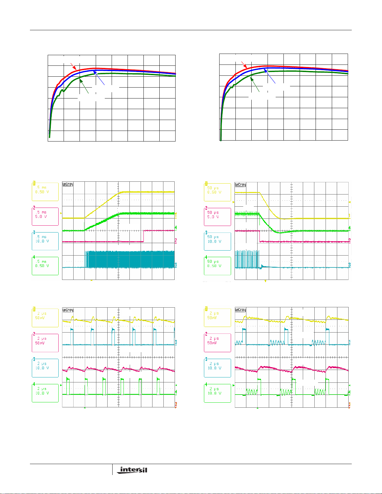
FIGURE 9. CHANNEL 1 EFFICIENCY AT VO=1.5V
V
O1
FB1
PGOOD1
EFFICIENCY (%)
100
95
90
85
80
75
70
65
60
V
= 8V
IN
12V
V
IN =
VIN = 19V
012345678
I
(A)
OUT
FIGURE 10. CHANNEL 2 EFFICIENCY AT VO = 1.8V
V
O1
FB1
PGOOD1
PHASE1
FIGURE 11. START-UP, V
= 12V, LOAD = 0.25Ω, VO= 1.05V
IN
V
O1
PHASE1
V
O2
PHASE2
FIGURE 13. CCM STEADY-STA TE OPERA TION,V
V
= 1.5V, IO1=3A, VO2= 1.8A, IO2=4A
O1
IN
= 12V,
PHASE1
FIGURE 12. SHUT-DOWN, V
= 12V, IO= 10A, VO= 1.05V
IN
V
O1
PHASE1
V
O2
PHASE2
FIGURE 14. DCM STEADY-ST A TE OPERA TION,V
V
= 1.5V, IO1=1A, VO2= 1.8V, IO2=1A
O1
IN
= 12V,
14
FN9095.2
May 7, 2008
Page 15
Typical Performance (Continued)
ISL6228
I
O1
V
O1
PHASE1
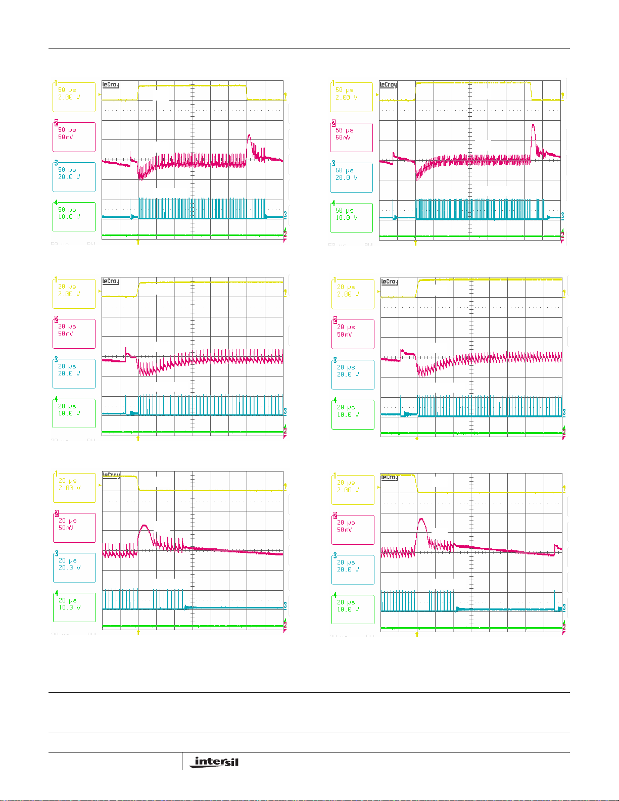
FIGURE 15. TRANSIENT RESPONSE, VIN= 12V, VO=1.5V,
I
= 0.1A/8.1A @ 2.55A/µs
O
I
O1
V
O1
FIGURE 16. TRANSIENT RESPONSE, V
I
= 0.1A/8.1A @ 2.55A/µs
O
I
O2
V
O2
I
O2
V
O2
PHASE2
= 12V, VO=1.8V,
IN
PHASE1
FIGURE 17. LOAD INSERTION RESPONSE, V
V
= 1.5V, IO= 0.1A/8.1A @ 2.55A/µs
O
I
O1
V
O1
PHASE1
FIGURE 19. LOAD RELEASE RESPONSE, V
V
= 1.5V, IO= 0.1A/8.1A @ 2.55A/µs
O
IN
IN
=12V,
= 12V,
FIGURE 18. LOAD INSERTION RESPONSE, V
V
= 1.8V, IO= 0.1A/8.1A @ 2.55A/µs
O
FIGURE 20. LOAD RELEASE RESPONSE, V
V
= 1.8V, IO= 0.1A/8.1A @ 2.55A/µs
O
PHASE2
I
O2
V
O2
PHASE2
IN
=12V,
IN
= 12V,
All Intersil U.S. products are manufactured, assembled and tested utilizing ISO9000 quality systems.
Intersil Corporation’s quality certifications can be viewed at www.intersil.com/design/quality
Intersil products are sold by description only. Intersil Corporation reserves the right to make changes in circuit design, software and/or specifications at any time without
notice. Accordingly, the reader is cautioned to verify that data sheets are current before placing orders. Information furnished by Intersil is believed to be accurate and
reliable. However, no responsibility is assumed by Intersil or its subsidiaries for its use; nor for any infringements of patents or other rights of third parties which may result
from its use. No license is granted by implicat ion or oth erwise u nde r any p a tent or p at ent r ights of Intersil or its subsidiaries.
For information regarding Intersil Corporation and its products, see www.intersil.com
15
FN9095.2
May 7, 2008
Page 16
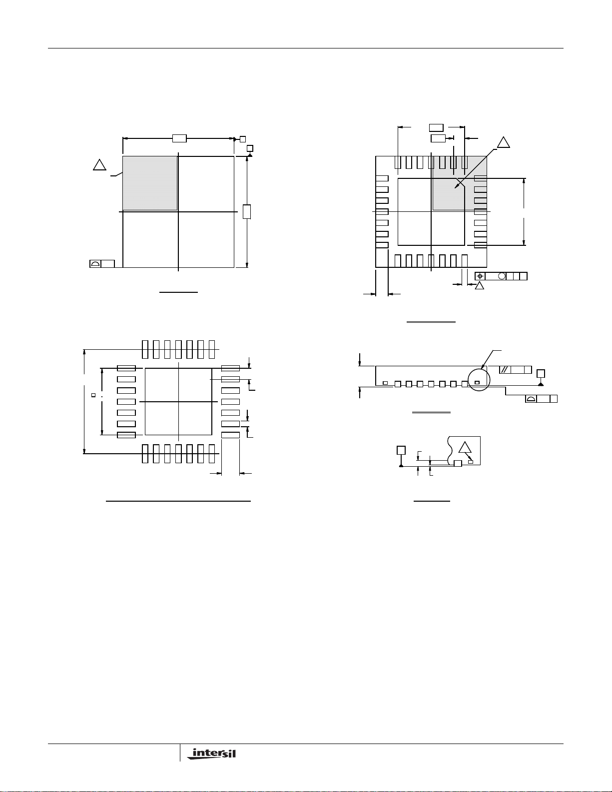
Package Outline Drawing
L28.4x4A
28 LEAD QUAD FLAT NO-LEAD PLASTIC PACKAGE
Rev 0, 3/07
4.00
6
PIN 1
INDEX AREA
ISL6228
4X
2.4
0.40
A
B
21
24X
22
28
6
PIN #1 INDEX AREA
1
(4X) 0.15
( 3. 75 TYP )
( 2. 40 )
TOP VIEW
TYPICAL RECOMMENDED LAND PATTERN
4.00
( 24X 0 . 4 )
( 28X 0 . 20 )
( 28X 0 . 65)
0 . 75
2 .40 ± 0 . 15
15
14
28X 0.45 ± 0.10
BOTTOM VIEW
SIDE VIEW
0 . 2 REF
C
DETAIL "X"
0 . 00 MIN.
0 . 05 MAX.
8
5
0.10 B
4
28X 0.20
BASE PLANE
ACM
SEE DETAIL "X"
C
0.10
C
SEATING PLANE
0.08 C
16
NOTES:
Dimensions are in millimeters.1.
Dimensions in ( ) for Reference Only.
2.
Dimensioning and tolerancing conform to AMSE Y14.5m-1994.
3.
Unless otherwise specified, tolerance : Decimal ± 0.05
4.
Dimension b applies to the metallized terminal and is measured
between 0.15mm and 0.30mm from the terminal tip.
Tiebar shown (if present) is a non-functional feature.
5.
The configuration of the pin #1 identifier is optional, but must be
6.
located within the zone indicated. The pin #1 identifier may be
either a mold or mark feature.
FN9095.2
May 7, 2008
 Loading...