


Intersil ISL61851ACBZ, ISL61851AIBZ, ISL61851BCBZ, ISL61851BIBZ, ISL61851CCBZ Schematic [ru]
...Dual USB Port Power Supply Controller
ISL6185
The ISL6185 USB power controller family provides fully independent overcurrent (OC) fault protection for two or more USB ports.
This product family consists of sixteen individual functional product variants and three package options. It is operation rated for a nominal +2.5V to +5V range and is specified over the full commercial and industrial temperature ranges.
Each ISL6185 type incorporates in a single package two 71mΩ P-channel MOSFET power switches for power control. Each features internal current monitoring, accurate current limiting, and current limited delay to turn-off, for system supply protection along with control and communication I/O.
The ISL6185 family offers product variants with specified continuous output current levels of 0.6A, 1.1A, 1.5A or 1.8A; enable active high or low inputs; and latch off or automatic retry after overcurrent turn-off, making these devices well suited for many low-power applications.
This family of ICs is offered in an industry-standard SOIC pinout and also in the 70% smaller 3x3 DFN packages providing similar or enhanced performance in the smallest possible package.
Features
•2.5V to 5V Operating Range
•71mΩ Integrated Power P-channel MOSFET Switches
•Continuous Current Options for 0.6A, 1.1A, 1.5A and 1.8A
•Thermally Insensitive 12ms of Current Limiting Prior to Turn-Off
•Output Discharges with Reverse Current Blocking When Disabled
•Latch-off or Auto Restart Options
•1µA Off-State Supply Current
•Enable Polarity Options
•Industry-standard Pin for Pin SOIC, and Smaller DFN Packages Available
•UL Recognized, File Number: E333469
Applications
•USB 1, 2, 3 Port Power Management
•Low Power (18W) Electronic Circuit Limiting and Breaker
|
|
|
|
|
|
|
|
|
|
D+ |
|
|
|
|
|
|
|
|
|
|
|
|
|
|
|
|
|
|
|
|
|
|
|
|
|
|
|
|
|
|
|
|
|
D- |
|
|
|
|
|
|
|
|
|
|
|
|
|
|
|
|
|
|
USB |
|
|||
|
|
|
|
|
|
|
|
|
|
|
|
|
|
|
|
|
|
|
|
|
|
|
|
|
|
|
|
|
|
|
|||
U |
|
|
|
|
|
|
|
|
|
|
|
|
|
|
|
|
|
|
|
|
|
|
|
|
|
|
|
|
|
PORT 1 |
|
||
|
|
|
|
|
|
|
|
|
|
|
|
|
|
|
|
|
|
|
|
|
|
|
|
|
|
|
|
|
|
|
|
|
|
S |
|
|
|
|
|
|
|
|
|
|
OUT_1 |
|
|
|
|
|
|
|
|
|
|
|
|
|
|
|
|
|
VBUS |
|
|||
B |
|
|
|
|
|
|
|
|
ENABLE_1 |
|
|
|
|
|
|
|
|
|
|
|
|
|
|
|
|
|
|
|
|
|
|
||
|
|
|
|
|
|
|
|
|
|
|
|
|
|
|
|
|
|
|
|
|
|
|
|
|
|
|
|
|
|
|
|||
C |
|
|
|
|
|
|
|
|
FAULT_1 |
|
|
|
|
|
|
|
|
|
|
|
|
|
|
|
|
|
|
|
|
|
|
|
|
|
|
|
|
|
|
|
|
|
|
|
|
|
|
|
|
|
|
|
|
|
|
|
|
|
|
|
|
|
|
|
|||
O |
|
|
|
|
|
|
|
|
|
|
|
|
|
|
|
|
|
|
|
|
|
|
|
|
|
|
|
|
|
|
|
|
|
N |
+5V |
|
|
|
|
|
|
|
VIN |
GND |
|
|
|
|
|
|
|
|
|
|
|
|
|
|
|
|
|
|
|
|
|
||
T |
|
|
|
|
|
|
|
|
|
|
|
|
|
|
|
|
|
|
|
|
|
|
|
|
|
|
|
|
|
|
|
|
|
R |
|
|
|
|
|
|
|
|
ISL6185 |
|
|
|
|
|
|
|
|
|
|
|
|
|
|
|
|
|
|
|
|
|
|
||
|
|
|
|
|
|
|
|
|
|
|
|
|
|
|
|
|
|
|
|
|
|
|
|
|
|
|
|
|
|
||||
O |
|
|
|
|
|
|
|
|
|
|
|
|
|
|
|
|
|
|
|
|
|
|
|
|
|
|
|
|
|
|
|
|
|
L |
|
|
|
|
|
|
|
|
|
|
|
|
|
|
|
|
|
|
|
|
|
|
|
|
|
|
|
|
|
|
|
|
|
|
|
|
|
|
|
|
|
FAULT_2 |
|
|
|
|
|
|
|
|
|
|
|
|
|
|
|
|
|
|
|
|
|
|
|||
L |
|
|
|
|
|
|
|
|
|
|
|
|
|
|
|
|
|
|
|
|
|
|
|
|
|
|
|
|
|
|
|||
E |
|
|
|
|
|
|
|
|
|
|
|
|
|
|
|
|
|
|
|
|
|
|
|
|
|
|
|
|
|
|
|
|
|
R |
|
|
|
|
|
|
|
|
ENABLE_2 OUT_2 |
|
|
|
|
|
|
|
|
|
|
|
|
|
|
|
|
|
|
|
|
|
|||
|
|
|
|
|
|
|
|
|
|
|
|
|
|
|
|
|
|
|
|
|
|
|
|
|
VBUS |
|
|||||||
|
|
|
|
|
|
|
|
|
|
|
|
|
|
|
|
|
|
|
|
|
|
|
|
|
|
|
|
|
|
USB |
|
||
|
|
|
|
|
|
|
|
|
|
|
|
|
|
|
|
|
|
|
|
|
|
|
|
|
|
|
|
|
|
|
|||
|
|
|
|
|
|
|
|
|
|
|
|
|
|
|
|
|
|
|
|
|
|
|
|
|
|
|
|
|
|
|
|||
|
|
|
|
|
|
|
|
|
|
|
|
|
|
|
|
|
|
|
|
|
|
|
|
|
|
|
|
|
|
PORT_2 |
|
||
|
|
|
|
|
|
|
|
|
|
D+ |
|
|
|
|
|
|
|
|
|
|
|
|
|
|
|
|
|
|
|
||||
|
|
|
|
|
|
|
|
|
|
|
|
|
|
|
|
|
|
|
|
|
|
|
|
|
|
|
|
|
|
|
|
||
|
|
|
|
|
|
|
|
|
|
D- |
|
|
|
|
|
|
|
|
|
|
|
|
|
|
|
|
|
|
|
|
|
|
|
|
|
|
|
|
|
|
|
USB PORT POWER |
|
|
|
|
|
|
|
|
|
|
|
|
|
|
|
|
|
|
|
|
|
||||
FIGURE 1. TYPICAL APPLICATION
|
1.3 |
|
|
|
|
|
|
|
|
DS(ON) |
1.2 |
|
|
|
|
|
|
|
|
1.1 |
|
|
|
|
|
|
|
|
|
r |
|
|
|
|
|
|
|
|
|
NORMALIZED |
1.0 |
|
|
|
|
|
|
|
|
0.9 |
|
|
|
|
|
|
|
|
|
0.8 |
|
|
|
|
|
|
|
|
|
|
|
|
|
|
|
|
|
|
|
|
0.7 |
-40 |
-25 |
0 |
25 |
45 |
75 |
85 |
115 |
|
|
|
|
TEMPERATURE (°C) |
|
|
|||
FIGURE 2. NORMALIZED rDS(ON) TEMPERATURE
CHARACTERISTIC CURVE
March 8, 2012 |
1 |
CAUTION: These devices are sensitive to electrostatic discharge; follow proper IC Handling Procedures. |
FN6937.3 |
|
1-888-INTERSIL or 1-888-468-3774 |Copyright Intersil Americas Inc. 2010, 2011, 2012. All Rights Reserved |
|
||
|
|
Intersil (and design) is a trademark owned by Intersil Corporation or one of its subsidiaries. |
All other trademarks mentioned are the property of their respective owners.

|
ISL6185 |
|
Simplified Block Diagram |
|
|
|
CHANNEL 1 LIKE CHANNEL 2 |
|
GND |
|
FAULT_1 |
|
- |
|
|
-V |
|
|
+ comp |
|
VIN |
|
OUT_1 |
POR |
|
|
EN_1 |
CURRENT AND TEMP. |
OUT_2 |
|
MONITORING, GATE, |
|
|
DELAY & OUTPUT CONTROL |
|
|
LOGIC |
|
EN_2 |
|
FAULT_2 |
Ordering Information
|
|
|
|
|
|
|
|
|
|
VIN = 5V |
|
|
|
|
PART |
|
|
|
|
|
|
|
|
|
MAXIMUM |
|
|
|
|
NUMBER |
|
EN/EN |
|
CONTINUOUS IOUT |
LATCH/AUTO |
TEMP. |
PACKAGE |
PKG. |
||||||
(Notes 1, 2, 3) |
PART MARKING |
INPUT |
|
(A) |
RETRY |
RANGE (°C) |
(Pb-free) |
DWG. # |
||||||
|
|
|
|
|
|
|
|
|
|
|||||
ISL61851ACBZ |
61851A CBZ |
|
EN |
|
0.6 |
LATCH |
0 to +70 |
8 Lead SOIC |
M8.15 |
|||||
|
|
|
|
|
|
|
|
|
||||||
ISL61851BCBZ |
61851B CBZ |
EN |
|
0.6 |
RETRY |
0 to +70 |
8 Lead SOIC |
M8.15 |
||||||
|
|
|
|
|
|
|
|
|
|
|||||
ISL61851CCBZ |
61851C CBZ |
|
EN |
|
1.1 |
LATCH |
0 to +70 |
8 Lead SOIC |
M8.15 |
|||||
|
|
|
|
|
|
|
|
|
|
|
||||
ISL61851DCBZ |
61851D CBZ |
|
|
EN |
|
1.1 |
RETRY |
0 to +70 |
8 Lead SOIC |
M8.15 |
||||
|
|
|
|
|
|
|
|
|
|
|
|
|
|
|
ISL61851ECBZ |
61851E CBZ |
|
|
|
|
|
|
|
|
0.6 |
LATCH |
0 to +70 |
8 Lead SOIC |
M8.15 |
EN |
||||||||||||||
|
|
|
|
|
|
|
|
|
|
|
|
|
||
ISL61851FCBZ |
61851F CBZ |
|
|
|
|
|
|
|
|
0.6 |
RETRY |
0 to +70 |
8 Lead SOIC |
M8.15 |
|
EN |
|||||||||||||
|
|
|
|
|
|
|
|
|
|
|
|
|
||
ISL61851GCBZ |
61851G CBZ |
|
|
|
|
|
|
|
|
1.1 |
LATCH |
0 to +70 |
8 Lead SOIC |
M8.15 |
EN |
||||||||||||||
|
|
|
|
|
|
|
|
|
|
|
|
|
||
ISL61851HCBZ |
61851H CBZ |
|
|
|
|
|
|
|
|
1.1 |
RETRY |
0 to +70 |
8 Lead SOIC |
M8.15 |
|
EN |
|||||||||||||
|
|
|
|
|
|
|
|
|
||||||
ISL61851ICBZ |
61851I CBZ |
EN |
|
1.5 |
LATCH |
0 to +70 |
8 Lead SOIC |
M8.15 |
||||||
|
|
|
|
|
|
|
|
|
||||||
ISL61851JCBZ |
61851J CBZ |
EN |
|
1.5 |
RETRY |
0 to +70 |
8 Lead SOIC |
M8.15 |
||||||
|
|
|
|
|
|
|
|
|
|
|
|
|
||
ISL61851KCBZ |
61851K CBZ |
|
|
|
|
|
|
|
|
1.5 |
LATCH |
0 to +70 |
8 Lead SOIC |
M8.15 |
|
EN |
|||||||||||||
|
|
|
|
|
|
|
|
|
|
|
|
|
||
ISL61851LCBZ |
61851L CBZ |
|
|
|
|
|
|
|
|
1.5 |
RETRY |
0 to +70 |
8 Lead SOIC |
M8.15 |
|
EN |
|||||||||||||
|
|
|
|
|
|
|
|
|
|
|
||||
ISL61852ACRZ |
52AC |
|
|
EN |
|
0.6 |
LATCH |
0 to +70 |
8 Lead DFN |
L8.3x3J |
||||
|
|
|
|
|
|
|
|
|
|
|||||
ISL61852BCRZ |
52BC |
|
EN |
|
0.6 |
RETRY |
0 to +70 |
8 Lead DFN |
L8.3x3J |
|||||
|
|
|
|
|
|
|
|
|
|
|
|
|||
ISL61852CCRZ |
52CC |
|
|
|
EN |
|
1.1 |
LATCH |
0 to +70 |
8 Lead DFN |
L8.3x3J |
|||
|
|
|
|
|
|
|
|
|
|
|
|
|||
ISL61852DCRZ |
52DC |
|
|
|
EN |
|
1.1 |
RETRY |
0 to +70 |
8 Lead DFN |
L8.3x3J |
|||
|
|
|
|
|
|
|
|
|
|
|
|
|
||
ISL61852ECRZ |
52EC |
|
|
|
|
|
|
|
|
0.6 |
LATCH |
0 to +70 |
8 Lead DFN |
L8.3x3J |
|
|
EN |
||||||||||||
|
|
|
|
|
|
|
|
|
|
|
|
|
|
|
2 |
|
FN6937.3 |
|
||
|
|
March 8, 2012 |
|

ISL6185
Ordering Information (Continued)
|
|
|
|
|
|
|
|
|
|
|
|
|
|
VIN = 5V |
|
|
|
|
PART |
|
|
|
|
|
|
|
|
|
|
|
|
|
MAXIMUM |
|
|
|
|
NUMBER |
|
|
|
|
CONTINUOUS IOUT |
LATCH/AUTO |
TEMP. |
PACKAGE |
PKG. |
|||||||||
|
EN/EN |
|||||||||||||||||
(Notes 1, 2, 3) |
PART MARKING |
INPUT |
|
(A) |
RETRY |
RANGE (°C) |
(Pb-free) |
DWG. # |
||||||||||
|
|
|
|
|
|
|
|
|
|
|
|
|
|
|
|
|
|
|
ISL61852FCRZ |
52FC |
|
|
|
|
|
|
|
|
|
|
|
|
0.6 |
RETRY |
0 to +70 |
8 Lead DFN |
L8.3x3J |
|
|
|
EN |
|||||||||||||||
|
|
|
|
|
|
|
|
|
|
|
|
|
|
|
|
|
|
|
ISL61852GCRZ |
52GC |
|
|
|
|
|
|
|
|
|
|
|
|
1.1 |
LATCH |
0 to +70 |
8 Lead DFN |
L8.3x3J |
|
|
|
EN |
|||||||||||||||
|
|
|
|
|
|
|
|
|
|
|
|
|
|
|
|
|
|
|
ISL61852HCRZ |
52HC |
|
|
|
|
|
|
|
|
|
|
|
|
1.1 |
RETRY |
0 to +70 |
8 Lead DFN |
L8.3x3J |
|
|
|
EN |
|||||||||||||||
|
|
|
|
|
|
|
|
|
|
|||||||||
ISL61852ICRZ |
52IC |
|
EN |
|
1.5 |
LATCH |
0 to +70 |
8 Lead DFN |
L8.3x3J |
|||||||||
|
|
|
|
|
|
|
|
|
|
|||||||||
ISL61852JCRZ |
52JC |
|
EN |
|
1.5 |
RETRY |
0 to +70 |
8 Lead DFN |
L8.3x3J |
|||||||||
|
|
|
|
|
|
|
|
|
|
|
|
|
|
|
|
|
|
|
ISL61852KCRZ |
52KC |
|
|
|
|
|
|
|
|
|
|
|
1.5 |
LATCH |
0 to +70 |
8 Lead DFN |
L8.3x3J |
|
|
|
|
EN |
|||||||||||||||
|
|
|
|
|
|
|
|
|
|
|
|
|
|
|
|
|
|
|
ISL61852LCRZ |
52LC |
|
|
|
|
|
|
|
|
|
|
|
|
1.5 |
RETRY |
0 to +70 |
8 Lead DFN |
L8.3x3J |
|
|
|
|
EN |
||||||||||||||
|
|
|
|
|
|
|
|
|
|
|
|
|||||||
ISL61853ACRZ |
53AC |
|
|
|
EN |
|
0.6 |
LATCH |
0 to +70 |
10 Lead DFN |
L10.3x3 |
|||||||
|
|
|
|
|
|
|
|
|
|
|||||||||
ISL61853BCRZ |
53BC |
|
EN |
|
0.6 |
RETRY |
0 to +70 |
10 Lead DFN |
L10.3x3 |
|||||||||
|
|
|
|
|
|
|
|
|
|
|
|
|
|
|||||
ISL61853CCRZ |
53CC |
|
|
|
|
|
EN |
|
1.1 |
LATCH |
0 to +70 |
10 Lead DFN |
L10.3x3 |
|||||
|
|
|
|
|
|
|
|
|
|
|
|
|
|
|||||
ISL61853DCRZ |
53DC |
|
|
|
|
|
EN |
|
1.1 |
RETRY |
0 to +70 |
10 Lead DFN |
L10.3x3 |
|||||
|
|
|
|
|
|
|
|
|
|
|
|
|
|
|
|
|
||
ISL61853ECRZ |
53EC |
|
|
|
|
|
|
|
|
|
|
|
|
0.6 |
LATCH |
0 to +70 |
10 Lead DFN |
L10.3x3 |
|
|
|
|
EN |
||||||||||||||
|
|
|
|
|
|
|
|
|
|
|
|
|
|
|
|
|||
ISL61853FCRZ |
53FC |
|
|
|
|
|
|
|
|
|
|
|
|
0.6 |
RETRY |
0 to +70 |
10 Lead DFN |
L10.3x3 |
|
|
|
|
EN |
||||||||||||||
|
|
|
|
|
|
|
|
|
|
|
|
|
|
|
|
|||
ISL61853GCRZ |
53GC |
|
|
|
|
|
|
|
|
|
|
|
1.1 |
LATCH |
0 to +70 |
10 Lead DFN |
L10.3x3 |
|
|
|
|
EN |
|||||||||||||||
|
|
|
|
|
|
|
|
|
|
|
|
|
|
|
||||
ISL61853HCRZ |
53HC |
|
|
|
|
|
|
|
|
|
|
|
1.1 |
RETRY |
0 to +70 |
10 Lead DFN |
L10.3x3 |
|
|
|
|
EN |
|||||||||||||||
|
|
|
|
|
|
|
|
|
|
|||||||||
ISL61853ICRZ |
53IC |
|
EN |
|
1.5 |
LATCH |
0 to +70 |
10 Lead DFN |
L10.3x3 |
|||||||||
|
|
|
|
|
|
|
|
|
|
|||||||||
ISL61853JCRZ |
53JC |
|
EN |
|
1.5 |
RETRY |
0 to +70 |
10 Lead DFN |
L10.3x3 |
|||||||||
|
|
|
|
|
|
|
|
|
|
|
|
|
|
|
||||
ISL61853KCRZ |
53KC |
|
|
|
|
|
|
|
|
|
|
1.5 |
LATCH |
0 to +70 |
10 Lead DFN |
L10.3x3 |
||
|
|
|
EN |
|||||||||||||||
|
|
|
|
|
|
|
|
|
|
|
|
|
|
|
|
|||
ISL61853LCRZ |
53LC |
|
|
|
|
|
|
|
|
|
|
|
1.5 |
RETRY |
0 to +70 |
10 Lead DFN |
L10.3x3 |
|
|
|
|
|
EN |
||||||||||||||
|
|
|
|
|
|
|
|
|
|
|||||||||
ISL61853MCRZ |
53MC |
|
EN |
|
1.8 |
LATCH |
0 to +70 |
10 Lead DFN |
L10.3x3 |
|||||||||
|
|
|
|
|
|
|
|
|
|
|||||||||
ISL61853NCRZ |
53NC |
|
EN |
|
1.8 |
RETRY |
0 to +70 |
10 Lead DFN |
L10.3x3 |
|||||||||
|
|
|
|
|
|
|
|
|
|
|
|
|
|
|
|
|||
ISL61853OCRZ |
53OC |
|
|
|
|
|
|
|
|
|
|
1.8 |
LATCH |
0 to +70 |
10 Lead DFN |
L10.3x3 |
||
|
|
|
|
EN |
||||||||||||||
|
|
|
|
|
|
|
|
|
|
|
|
|
|
|
|
|||
ISL61853PCRZ |
53PC |
|
|
|
|
|
|
|
|
|
|
|
1.8 |
RETRY |
0 to +70 |
10 Lead DFN |
L10.3x3 |
|
|
|
|
EN |
|||||||||||||||
|
|
|
|
|
|
|
|
|
|
|||||||||
ISL61851AIBZ |
61851A IBZ |
|
EN |
|
0.6 |
LATCH |
-40 to +85 |
8 Lead SOIC |
M8.15 |
|||||||||
|
|
|
|
|
|
|
|
|
||||||||||
ISL61851BIBZ |
61851B IBZ |
EN |
|
0.6 |
RETRY |
-40 to +85 |
8 Lead SOIC |
M8.15 |
||||||||||
|
|
|
|
|
|
|
|
|
|
|
||||||||
ISL61851CIBZ |
61851C IBZ |
|
|
EN |
|
1.1 |
LATCH |
-40 to +85 |
8 Lead SOIC |
M8.15 |
||||||||
|
|
|
|
|
|
|
|
|
|
|
|
|||||||
ISL61851DIBZ |
61851D IBZ |
|
|
|
EN |
|
1.1 |
RETRY |
-40 to +85 |
8 Lead SOIC |
M8.15 |
|||||||
|
|
|
|
|
|
|
|
|
|
|
|
|
|
|
||||
ISL61851EIBZ |
61851E IBZ |
|
|
|
|
|
|
|
|
|
|
0.6 |
LATCH |
-40 to +85 |
8 Lead SOIC |
M8.15 |
||
EN |
||||||||||||||||||
|
|
|
|
|
|
|
|
|
|
|
|
|
|
|||||
ISL61851FIBZ |
61851F IBZ |
|
|
|
|
|
|
|
|
|
|
0.6 |
RETRY |
-40 to +85 |
8 Lead SOIC |
M8.15 |
||
|
|
EN |
||||||||||||||||
|
|
|
|
|
|
|
|
|
|
|
|
|
|
|||||
ISL61851GIBZ |
61851G IBZ |
|
|
|
|
|
|
|
|
|
|
1.1 |
LATCH |
-40 to +85 |
8 Lead SOIC |
M8.15 |
||
EN |
||||||||||||||||||
|
|
|
|
|
|
|
|
|
|
|
|
|
|
|
||||
ISL61851HIBZ |
61851H IBZ |
|
|
|
|
|
|
|
|
|
|
1.1 |
RETRY |
-40 to +85 |
8 Lead SOIC |
M8.15 |
||
|
|
|
EN |
|||||||||||||||
|
|
|
|
|
|
|
|
|
||||||||||
ISL61851IIBZ |
61851I IBZ |
EN |
|
1.5 |
LATCH |
-40 to +85 |
8 Lead SOIC |
M8.15 |
||||||||||
|
|
|
|
|
|
|
|
|
||||||||||
ISL61851JIBZ |
61851J IBZ |
EN |
|
1.5 |
RETRY |
-40 to +85 |
8 Lead SOIC |
M8.15 |
||||||||||
|
|
|
|
|
|
|
|
|
|
|
|
|
||||||
ISL61851KIBZ |
61851K IBZ |
|
|
|
|
|
|
|
|
|
|
1.5 |
LATCH |
-40 to +85 |
8 Lead SOIC |
M8.15 |
||
|
EN |
|||||||||||||||||
|
|
|
|
|
|
|
|
|
|
|
|
|
|
|||||
ISL61851LIBZ |
61851L IBZ |
|
|
|
|
|
|
|
|
|
|
1.5 |
RETRY |
-40 to +85 |
8 Lead SOIC |
M8.15 |
||
|
|
EN |
||||||||||||||||
|
|
|
|
|
|
|
|
|
|
|
|
|
|
|||||
ISL61852AIRZ |
52AI |
|
|
|
|
|
EN |
|
0.6 |
LATCH |
-40 to +85 |
8 Lead DFN |
L8.3x3J |
|||||
|
|
|
|
|
|
|
|
|
||||||||||
ISL61852BIRZ |
52BI |
EN |
|
0.6 |
RETRY |
-40 to +85 |
8 Lead DFN |
L8.3x3J |
||||||||||
|
|
|
|
|
|
|
|
|
|
|
|
|
|
|||||
ISL61852CIRZ |
52CI |
|
|
|
|
|
EN |
|
1.1 |
LATCH |
-40 to +85 |
8 Lead DFN |
L8.3x3J |
|||||
|
|
|
|
|
|
|
|
|
|
|
|
|
|
|||||
ISL61852DIRZ |
52DI |
|
|
|
|
|
EN |
|
1.1 |
RETRY |
-40 to +85 |
8 Lead DFN |
L8.3x3J |
|||||
|
|
|
|
|
|
|
|
|
|
|
|
|
|
|
|
|||
ISL61852EIRZ |
52EI |
|
|
|
|
|
|
|
|
|
|
|
|
0.6 |
LATCH |
-40 to +85 |
8 Lead DFN |
L8.3x3J |
|
|
|
|
|
EN |
|||||||||||||
|
|
|
|
|
|
|
|
|
|
|
|
|
|
|
|
|
|
|
3 |
|
FN6937.3 |
|
||
|
|
March 8, 2012 |
|

ISL6185
Ordering Information (Continued)
|
|
|
|
|
|
|
|
|
|
VIN = 5V |
|
|
|
|
PART |
|
|
|
|
|
|
|
|
|
MAXIMUM |
|
|
|
|
NUMBER |
|
|
|
|
CONTINUOUS IOUT |
LATCH/AUTO |
TEMP. |
PACKAGE |
PKG. |
|||||
|
EN/EN |
|||||||||||||
(Notes 1, 2, 3) |
PART MARKING |
INPUT |
|
(A) |
RETRY |
RANGE (°C) |
(Pb-free) |
DWG. # |
||||||
|
|
|
|
|
|
|
|
|
|
|
|
|
|
|
ISL61852FIRZ |
52FI |
|
|
|
|
|
|
|
|
0.6 |
RETRY |
-40 to +85 |
8 Lead DFN |
L8.3x3J |
|
|
EN |
||||||||||||
|
|
|
|
|
|
|
|
|
|
|
|
|
|
|
ISL61852GIRZ |
52GI |
|
|
|
|
|
|
|
1.1 |
LATCH |
-40 to +85 |
8 Lead DFN |
L8.3x3J |
|
EN |
||||||||||||||
|
|
|
|
|
|
|
|
|
|
|
|
|
|
|
ISL61852HIRZ |
52HI |
|
|
|
|
|
|
|
1.1 |
RETRY |
-40 to +85 |
8 Lead DFN |
L8.3x3J |
|
|
|
EN |
||||||||||||
|
|
|
|
|
|
|
|
|
||||||
ISL61852IIRZ |
52II |
EN |
|
1.5 |
LATCH |
-40 to +85 |
8 Lead DFN |
L8.3x3J |
||||||
|
|
|
|
|
|
|
|
|
||||||
ISL61852JIRZ |
52JI |
EN |
|
1.5 |
RETRY |
-40 to +85 |
8 Lead DFN |
L8.3x3J |
||||||
|
|
|
|
|
|
|
|
|
|
|
|
|||
ISL61852KIRZ |
52KI |
|
|
|
|
|
|
1.5 |
LATCH |
-40 to +85 |
8 Lead DFN |
L8.3x3J |
||
|
EN |
|||||||||||||
|
|
|
|
|
|
|
|
|
|
|
|
|
||
ISL61852LIRZ |
52LI |
|
|
|
|
|
|
|
1.5 |
RETRY |
-40 to +85 |
8 Lead DFN |
L8.3x3J |
|
|
|
EN |
||||||||||||
|
|
|
|
|
|
|
|
|
|
|||||
ISL61853AIRZ |
53AI |
|
EN |
|
0.6 |
LATCH |
-40 to +85 |
10 Lead DFN |
L10.3x3 |
|||||
|
|
|
|
|
|
|
|
|
||||||
ISL61853BIRZ |
53BI |
EN |
|
0.6 |
RETRY |
-40 to +85 |
10 Lead DFN |
L10.3x3 |
||||||
|
|
|
|
|
|
|
|
|
|
|||||
ISL61853CIRZ |
53CI |
|
EN |
|
1.1 |
LATCH |
-40 to +85 |
10 Lead DFN |
L10.3x3 |
|||||
|
|
|
|
|
|
|
|
|
|
|||||
ISL61853DIRZ |
53DI |
|
EN |
|
1.1 |
RETRY |
-40 to +85 |
10 Lead DFN |
L10.3x3 |
|||||
|
|
|
|
|
|
|
|
|
|
|
|
|
||
ISL61853EIRZ |
53EI |
|
|
|
|
|
|
|
0.6 |
LATCH |
-40 to +85 |
10 Lead DFN |
L10.3x3 |
|
|
|
EN |
||||||||||||
|
|
|
|
|
|
|
|
|
|
|
|
|
||
ISL61853FIRZ |
53FI |
|
|
|
|
|
|
|
|
0.6 |
RETRY |
-40 to +85 |
10 Lead DFN |
L10.3x3 |
|
|
EN |
||||||||||||
|
|
|
|
|
|
|
|
|
|
|
|
|
||
ISL61853GIRZ |
53GI |
|
|
|
|
|
|
|
1.1 |
LATCH |
-40 to +85 |
10 Lead DFN |
L10.3x3 |
|
|
EN |
|||||||||||||
|
|
|
|
|
|
|
|
|
|
|
|
|
||
ISL61853HIRZ |
53HI |
|
|
|
|
|
|
|
1.1 |
RETRY |
-40 to +85 |
10 Lead DFN |
L10.3x3 |
|
|
|
EN |
||||||||||||
|
|
|
|
|
|
|
|
|
||||||
ISL61853IIRZ |
53II |
EN |
|
1.5 |
LATCH |
-40 to +85 |
10 Lead DFN |
L10.3x3 |
||||||
|
|
|
|
|
|
|
|
|
||||||
ISL61853JIRZ |
53JI |
EN |
|
1.5 |
RETRY |
-40 to +85 |
10 Lead DFN |
L10.3x3 |
||||||
|
|
|
|
|
|
|
|
|
|
|
|
|||
ISL61853KIRZ |
53KI |
|
|
|
|
|
|
1.5 |
LATCH |
-40 to +85 |
10 Lead DFN |
L10.3x3 |
||
|
EN |
|||||||||||||
|
|
|
|
|
|
|
|
|
|
|
|
|
||
ISL61853LIRZ |
53LI |
|
|
|
|
|
|
|
1.5 |
RETRY |
-40 to +85 |
10 Lead DFN |
L10.3x3 |
|
|
|
EN |
||||||||||||
|
|
|
|
|
|
|
|
|
||||||
ISL61853MIRZ |
53MI |
EN |
|
1.8 |
LATCH |
-40 to +85 |
10 Lead DFN |
L10.3x3 |
||||||
|
|
|
|
|
|
|
|
|
||||||
ISL61853NIRZ |
53NI |
EN |
|
1.8 |
RETRY |
-40 to +85 |
10 Lead DFN |
L10.3x3 |
||||||
|
|
|
|
|
|
|
|
|
|
|
|
|
||
ISL61853OIRZ |
53OI |
|
|
|
|
|
|
1.8 |
LATCH |
-40 to +85 |
10 Lead DFN |
L10.3x3 |
||
|
|
EN |
||||||||||||
|
|
|
|
|
|
|
|
|
|
|
|
|
||
ISL61853PIRZ |
53PI |
|
|
|
|
|
|
|
1.8 |
RETRY |
-40 to +85 |
10 Lead DFN |
L10.3x3 |
|
|
EN |
|||||||||||||
|
|
|
|
|
|
|
|
|||||||
ISL61851EVAL1Z |
8 Lead SOIC Evaluation Platform with ISL61851A installed |
|
|
|
||||||||||
|
|
|
|
|
||||||||||
ISL61852EVAL1Z |
8 Lead DFN Evaluation Platform with ISL61852H installed |
|
|
|
||||||||||
|
|
|
|
|
||||||||||
ISL61853EVAL1Z |
10 Lead DFN Evaluation Platform with ISL61853I installed |
|
|
|
||||||||||
|
|
|
|
|
|
|
|
|
|
|
|
|
|
|
NOTES:
1.Add “-T*” suffix for tape and reel. Please refer to TB347 for details on reel specifications.
2.These Intersil Pb-free plastic packaged products employ special Pb-free material sets, molding compounds/die attach materials, and 100% matte tin plate plus anneal (e3 termination finish, which is RoHS compliant and compatible with both SnPb and Pb-free soldering operations). Intersil Pbfree products are MSL classified at Pb-free peak reflow temperatures that meet or exceed the Pb-free requirements of IPC/JEDEC J STD-020.
3.For Moisture Sensitivity Level (MSL), please see device information pages for ISL6185XXC (commercial version) and ISL6185XXI (industrial version). For more information on MSL please see techbrief TB363.
4 |
|
FN6937.3 |
|
||
|
|
March 8, 2012 |
|
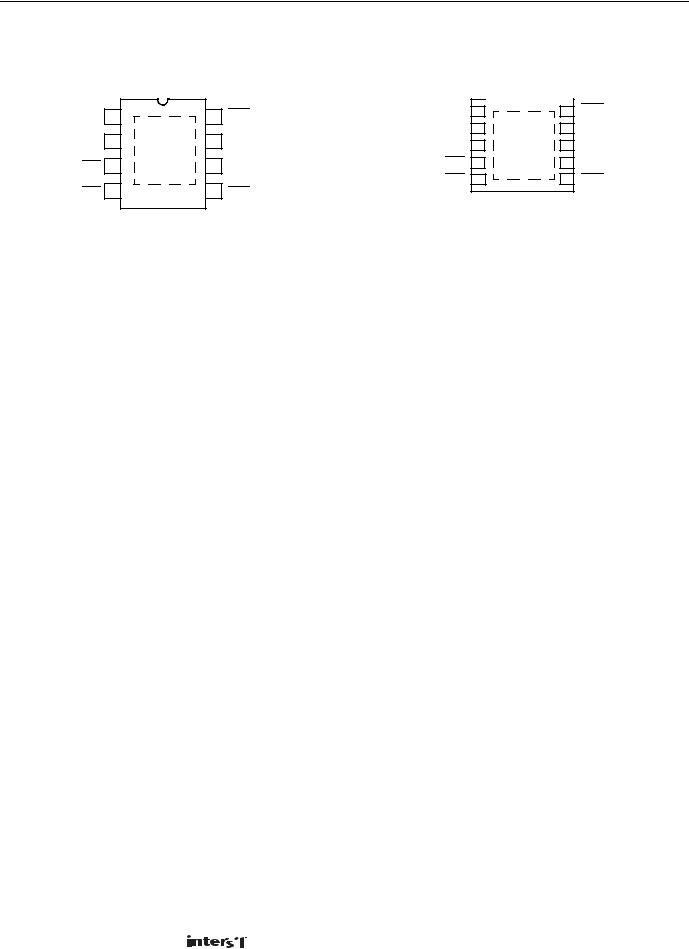
ISL6185
Pin Configurations
|
|
ISL6185 |
|
|
|
|
(8 LD SOIC/DFN) |
|
|
|
|
TOP VIEW |
|
|
GND |
1 |
|
8 |
FLT1 |
VIN |
2 |
(GND) |
7 |
OUT1 |
EPAD |
||||
EN1/EN1 |
3 |
DFN Only |
6 |
OUT2 |
|
||||
EN2/EN2 |
4 |
|
5 |
FLT2 |
|
|
ISL6185 |
|
|
|
|
|
(10 LD DFN) |
|
|
|
|
|
TOP VIEW |
|
|
|
GND |
1 |
|
10 |
FLT1 |
|
VIN |
2 |
(GND) |
9 |
OUT1 |
|
VIN |
3 |
8 |
NC |
||
EPAD |
|||||
EN1/EN1 |
4 |
7 |
OUT2 |
||
|
|||||
EN2/EN2 |
5 |
|
6 |
FLT2 |
Pin Descriptions
PIN NUMBER |
|
|
|
|
|
|
|
|
|
|
|
|
|
|
|
|
|
|
|
|
|
|
|
|
|
|
|
|
|
|
|
8 Ld |
|
|
|
|
|
|
|
|
|
|
|
|
|
|
|
SOIC/DFN |
10 Ld DFN |
SYMBOL |
|
|
|
|
DESCRIPTION |
||||||||
|
|
|
|
|
|||||||||||
1 |
1 |
|
GND |
IC ground reference. |
|||||||||||
|
|
|
|
|
|||||||||||
2 |
2, 3 |
|
VIN |
Chip bias, Controlled Voltage Input, Undervoltage Lock Out (UVLO). VIN provides chip bias voltage. At |
|||||||||||
|
|
|
|
|
|
|
|
|
VIN < 1.7V chip functionality is disabled, |
FLT |
is active and floating, and OUT is held low. Range 0V to |
||||
|
|
|
|
|
|
|
|
|
5.5V. |
||||||
|
|
|
|
|
|
|
|
|
|
|
|||||
3, |
4, |
EN1, |
|
|
|
|
|
Enable/Disable inputs, Active high (EN) and active low |
|
options enable the power switch. These |
|||||
EN1/ |
(EN) |
||||||||||||||
4 |
5 |
EN2, |
|
|
|
inputs have internal 1MΩ pull-off resistors. Range 0V to VIN. |
|||||||||
EN2 |
|||||||||||||||
|
|
|
|
|
|
|
|
||||||||
5, |
6, |
|
|
|
|
|
Overcurrent Fault Indicator. |
|
floats and is disabled until VIN >VUVLO. This output is pulled low after |
||||||
|
FLT2 |
FLT |
|||||||||||||
8 |
10 |
|
FLT1 |
|
the current limit time-out period has expired. Fault is not signaled due to over-temperature shut down. |
||||||||||
|
|
|
|
|
|
|
|
|
Range 0V to VIN. |
||||||
|
|
|
|
||||||||||||
6, |
7, |
OUT2, |
Controlled Supply Output. Upon an OC condition, IOUT is current limited. Current limit response time is |
||||||||||||
7 |
9 |
OUT1 |
within 200µs. This output remains in current limit for a nominal 12ms before being turned off either for |
||||||||||||
|
|
|
|
|
|
|
|
|
the latch or auto retry versions. Range 0V to VIN. |
||||||
|
|
|
|
|
|||||||||||
- |
8 |
|
NC |
This pin is not electrically connected internally. |
|||||||||||
|
|
|
|
||||||||||||
PD |
PD |
EPAD |
Thermal Dissipation Exposed PAD Range: Connect to GND. |
||||||||||||
(DFN only) |
|
|
|
|
|
|
|
|
|
|
|
|
|
|
|
|
|
|
|
|
|
|
|
|
|
|
|
|
|
|
|
5 |
|
FN6937.3 |
|
||
|
|
March 8, 2012 |
|

ISL6185
Absolute Maximum Ratings
Supply Voltage (VIN to GND, Note 7) . . . . . . . . . . . . . . . . . . . . . . . . . . . .6.5V EN, FAULT. . . . . . . . . . . . . . . . . . . . . . . . . . . . . . . . . . . . . . . . . . . . . . . . . . . .VIN OUT . . . . . . . . . . . . . . . . . . . . . . . . . . . . . . . . . . . . . . . . GND - 0.3V to VIN 0.3V Output Current . . . . . . . . . . . Short Circuit Protected Current Limit of 2.5A ESD Rating
Human Body Model (Per MIL-STD-883 Method 3015.7). . . . . . . . . . 3kV Machine Model (Per MIL-STD-883 Method 3015.7) . . . . . . . . . . . . 300V Latch Up (Tested per JESD-78B; Class 2, Level A) . . . . . . . . . . . . . . 100mA
Thermal Information
Thermal Resistance (Typical, Note 4) |
θJA (°C/W) |
θJC (°C/W) |
8 Lead SOIC Package (Note 4) . . . . . . . . . . |
120 |
N/A |
8 Lead 3x3 DFN Package (Notes 5, 6) . . . |
48 |
6 |
10 Lead 3x3 DFN Package (Notes 5, 6) . . |
53 |
6 |
Maximum Junction Temperature . . . . . . . . . . |
. . . . . . . . . . . . |
. . . . . +150°C |
Maximum Storage Temperature Range . . . . . |
. . . . . . . . . -65°C to +150°C |
|
Pb-Free Reflow Profile . . . . . . . . . . . . . . . . . . . . |
. . . . . . . . . . . . |
see link below |
http://www.intersil.com/pbfree/Pb-FreeReflow.asp
Operating Conditions
Commercial Temperature Range . . . . . . . . . . . . . . . . . . . . . . 0°C to +70°C
Industrial Temperature Range . . . . . . . . . . . . . . . . . . . . . . . -40°C to +85°C
Supply Voltage Range (Typical). . . . . . . . . . . . . . . . . . . . . . . . . 2.3V to 5.5V
CAUTION: Do not operate at or near the maximum ratings listed for extended periods of time. Exposure to such conditions may adversely impact product reliability and result in failures not covered by warranty.
NOTES:
4.θJA is measured with the component mounted on a high effective thermal conductivity test board in free air. See Tech Brief TB379 for details.
5.θJA is measured in free air with the component mounted on a high effective thermal conductivity test board with “direct attach” features. See Tech Brief TB379.
6.For θJC, the “case temp” location is the center of the exposed metal pad on the package underside.
7.All voltages are relative to GND, unless otherwise specified.
Electrical Specifications VIN = 5V, TA = TJ, Unless Otherwise Specified. Boldface limits apply over the operating temperature range, 0°C to +75°C or -40°C to +85°C.
|
|
|
|
MIN |
|
MAX |
|
SYMBOL |
|
PARAMETER |
TEST CONDITIONS |
(Note 8) |
TYP |
(Note 8) |
UNITS |
|
|
|
|
|
|
|
|
POWER SWITCH |
|
|
|
|
|
|
|
|
|
|
|
|
|
|
|
rDS(ON)_50 |
|
ON-Resistance at 5.0V (Pulse Tested) |
VIN = 5V, IOUT = 0.1A, TA = TJ = +25°C |
- |
71 |
87 |
mΩ |
|
|
|
TA = TJ = +85°C |
- |
|
110 |
mΩ |
rDS(ON)_33 |
|
ON-Resistance at 3.3V (Pulse Tested) |
VIN = 3.3V, IOUT = 0.1A, TA = TJ = +25°C |
- |
90 |
105 |
mΩ |
|
|
|
TA = TJ = +85°C |
- |
|
130 |
mΩ |
rDS(ON)_25 |
|
On Resistance at 2.5V (Pulse Tested) |
VIN = 2.5V, IOUT = 0.1A, TA = TJ = +25°C |
- |
114 |
127 |
mΩ |
|
|
|
TA = TJ = +85°C |
- |
|
150 |
mΩ |
VOUT_DIS |
|
Disabled Output Voltage |
VIN = 5V, Switch Disabled, 50µA Load |
- |
50 |
70 |
mV |
ROUT_PU |
|
Output Pull-Down Resistor |
VIN = 5V, Switch Disabled |
8 |
9.6 |
12 |
kΩ |
tR |
|
VOUT Rise Time |
RL = 10Ω,CL = 10µF, 10% to 90% |
- |
100 |
- |
µs |
tF |
|
Slow VOUT Turn-off Fall Time |
RL = 10Ω,CL = 10µF, 90% to 10% |
- |
200 |
- |
µs |
tF_fast |
|
Fast VOUT Turn-off Fall Time |
RL = 1Ω,CL = 10µF, 80% to 20% |
- |
23 |
- |
µs |
CURRENT CONTROL |
|
|
|
|
|
||
|
|
|
|
|
|
|
|
IOUT_CONT_5 |
|
Maximum Continuous Current, VIN = |
ISL6185xA,B,E,F |
- |
|
0.6 |
A |
|
|
5V. |
|
|
|
|
|
IOUT_CONT_5 |
|
ISL6185xC,D,G,H |
- |
|
1.1 |
A |
|
|
Guaranteed by Itrip minimum |
|
|||||
IOUT_CONT_5 |
|
specification. |
ISL6185xI,J,K,L |
- |
|
1.5 |
A |
IOUT_CONT_5 |
|
|
ISL61853M,N,O,P (10 Ld DFN) |
- |
|
1.8 |
A |
IOUT_CONT_3 |
|
Maximum Continuous Current, VIN = |
ISL6185xA,B,E,F |
- |
|
0.6 |
A |
|
|
3.3V. |
|
|
|
|
|
IOUT_CONT_3 |
|
ISL6185xC,D,G,H |
- |
|
0.9 |
A |
|
|
Guaranteed by Itrip minimum |
|
|||||
IOUT_CONT_3 |
|
specification. |
ISL61851I,J,K,L (SOIC) |
- |
|
1.3 |
A |
IOUT_CONT_3 |
|
|
ISL61852, ISL61853 (DFN) |
- |
|
1.5 |
A |
6 |
|
FN6937.3 |
|
||
|
|
March 8, 2012 |
|

ISL6185
Electrical Specifications VIN = 5V, TA = TJ, Unless Otherwise Specified. Boldface limits apply over the operating temperature range, 0°C to +75°C or -40°C to +85°C. (Continued)
|
|
|
MIN |
|
MAX |
|
|
SYMBOL |
PARAMETER |
TEST CONDITIONS |
(Note 8) |
TYP |
(Note 8) |
UNITS |
|
|
|
|
|
|
|
|
|
IOUT_CONT_2 |
Maximum Continuous Current, VIN = |
ISL6185xA,B,E,F |
- |
0.6 |
- |
A |
|
|
2.5V |
|
|
|
|
|
|
IOUT_CONT_2 |
ISL61851C,D,G,H,I,J,K,L (SOIC) |
- |
0.9 |
- |
A |
||
|
|||||||
IOUT_CONT_2 |
|
ISL61852, ISL61853 C,D,G,H (DFN) |
- |
1 |
- |
A |
|
IOUT_CONT_2 |
|
ISL61853I,J,K,L (10 Ld DFN) |
- |
1 |
- |
A |
|
IOUT_CONT_2 |
|
ISL61853M,N,O,P (10 Ld DFN) |
- |
1 |
- |
A |
|
ITRIP_5 |
Trip Current, VIN = 5V |
ISL6185xA,B,E,F |
0.70 |
1.02 |
1.52 |
A |
|
ITRIP_5 |
|
ISL6185xC,D,G,H |
1.15 |
1.45 |
1.95 |
A |
|
ITRIP_5 |
|
ISL6185xI,J,K,L |
1.55 |
1.82 |
2.25 |
A |
|
ITRIP_5 |
|
ISL61853M.N,O,P |
1.85 |
1.99 |
2.45 |
A |
|
ITRIP_3 |
Trip Current, VIN = 3.3V |
ISL6185xA,B,E,F |
0.65 |
0.86 |
1.20 |
A |
|
ITRIP_3 |
|
ISL6185xC,D,G,H |
0.95 |
1.25 |
1.60 |
A |
|
ITRIP_3 |
|
ISL6185xI,J,K,L |
1.35 |
1.60 |
1.85 |
A |
|
ITRIP_3 |
|
ISL61853M.N,O,P |
1.55 |
1.89 |
2.25 |
A |
|
ITRIP_2 |
Trip Current, VIN = 2.5V |
ISL6185xA,B,E,F |
- |
0.65 |
- |
A |
|
ITRIP_2 |
|
ISL6185xC,D,G,H |
- |
1 |
- |
A |
|
ITRIP_2 |
|
ISL6185xI,J,K,L |
- |
1.2 |
- |
A |
|
ITRIP_2 |
|
ISL61853M.N,O,P |
- |
1.6 |
- |
A |
|
ILIM_5 |
Current Limit, VIN = 5V |
ISL6185xA,B,E,F, VIN - VOUT = 1V |
0.50 |
0.65 |
0.78 |
A |
|
ILIM_5 |
|
ISL6185xC,D,G,H, VIN - VOUT = 1V |
0.98 |
1.14 |
1.28 |
A |
|
ILIM_5 |
|
ISL6185xI,J,K,L, VIN - VOUT = 1V |
1.30 |
1.55 |
1.72 |
A |
|
ILIM_5 |
|
ISL61853M,N,O,P, VIN - VOUT = 1V |
1.52 |
1.83 |
2.20 |
A |
|
ILIM_3 |
Current Limit, VIN = 3.3V |
ISL6185xA,B,E,F, VIN - VOUT = 1V |
0.45 |
0.63 |
0.75 |
A |
|
ILIM_3 |
|
ISL6185xC,D,G,H, VIN - VOUT = 1V |
0.90 |
1.10 |
1.26 |
A |
|
ILIM_3 |
|
ISL6185xI,J,K,L, VIN - VOUT = 1V |
1.25 |
1.50 |
1.68 |
A |
|
ILIM_3 |
|
ISL61853M,N,O,P, VIN - VOUT = 1V |
1.48 |
1.78 |
2.05 |
A |
|
ILIM_2 |
Current Limit, VIN = 2.5V |
ISL6185xA,B,E,F, VIN - VOUT = 1V |
0.47 |
0.61 |
0.74 |
A |
|
ILIM_2 |
|
ISL6185xC,D,G,H, VIN - VOUT = 1V |
0.90 |
1.05 |
1.17 |
A |
|
ILIM_2 |
|
ISL6185xI,J,K,L, VIN - VOUT = 1V |
1.15 |
1.37 |
1.58 |
A |
|
ILIM_2 |
|
ISL61853M,N,O,P, VIN - VOUT = 1V |
1.3 |
1.63 |
1.90 |
A |
|
Isc_5 |
Short Circuit Current, VIN = 5V |
ISL6185xA,B,E,F, VOUT = 0V |
0.60 |
0.80 |
1.00 |
A |
|
Isc_5 |
|
ISL6185xC,D,G,H, VOUT = 0V |
1.00 |
1.27 |
1.55 |
A |
|
Isc_5 |
|
ISL6185xI,J,K,L, VOUT = 0V |
1.15 |
1.61 |
1.85 |
A |
|
Isc_5 |
|
ISL61853M,N,O,P, VOUT = 0V |
1.20 |
1.70 |
2.5 |
A |
|
Isc_3 |
Short Circuit Current, VIN = 3.3V |
ISL6185XA,B,E,F, VOUT = 0V |
0.35 |
0.48 |
0.60 |
A |
|
Isc_3 |
|
ISL6185XC,D,G,H, VOUT = 0V |
0.65 |
0.80 |
0.95 |
A |
|
Isc_3 |
|
ISL6185xI,J,K,L, VOUT = 0V |
0.70 |
1.06 |
1.25 |
A |
|
Isc_3 |
|
ISL61853M,N,O,P, VOUT = 0V |
0.90 |
1.24 |
1.50 |
A |
7 |
|
FN6937.3 |
|
||
|
|
March 8, 2012 |
|
 Loading...