

Page 1
®
www.BDTIC.com/Intersil
HA-5127/883
Data Sheet FN3751.3January 16, 2006
Ultra Low Noise, Precision Operational
Amplifier
The HA-5127/883 monolithic operational amplifier features
an excellent combination of precision DC and wideband high
speed characteristics. Utilizing the Intersil D.I. technology
and advanced processing techniques, this unique design
unites low noise precision instrumentation performance with
high speed, wideband capability.
This amplifier’s impressive list of features include low V
OS
,
wide gain-bandwidth, high open loop gain, and high CMRR.
Additionally, this flexible device operates over a wide supply
range while consuming only 120mW of power.
Using the HA-5127/883 allows designers to minimize errors
while maximizing speed and bandwidth.
This device is ideally suited for low level transducer signal
amplifier circuits. Other applications which can utilize the
HA-5127/883’s qualities include instrumentation amplifiers,
pulse or RF amplifiers, audio preamplifiers, and signal
conditioning circuits.
Ordering Information
PART
NUMBER
HA2-5127/883 HA2-5127/883 -55 to +125 8 Pin Can T8.C
PAR T
MARKING
TEMP
RANGE
(°C) PACKAGE
PKG.
DWG. #
Features
• This Circuit is Processed in Accordance to MIL-STD-883
and is Fully Conformant Under the Provisions of
Paragraph 1.2.1.
• High Slew Rate . . . . . . . . . . . . . . . . . . . . . . . .7V/µs (Min)
• Unity Gain Bandwidth. . . . . . . . . . . . . . . . . . . .5MHz (Min)
• Low Noise Voltage (at 1kHz) . . . . . . . . . 4.5nV/√Hz
(Max)
• Low Offset Voltage . . . . . . . . . . . . . . . . . . . . .100µV (Max)
• Low Offset Drift With Temperature . . . . . . 1.8µV/oC (Max)
• High CMRR . . . . . . . . . . . . . . . . . . . . . . . . . . 100dB (Min)
• High Voltage Gain . . . . . . . . . . . . . . . . . . . 700kV/V (Min)
Applications
• High Speed Signal Conditioners
• Wide Bandwidth Instrumentation Amplifiers
• Low Level Transducer Amplifiers
• Fast, Low Level Voltage Comparators
• Highest Quality Audio Preamplifiers
• Pulse/RF Amplifiers
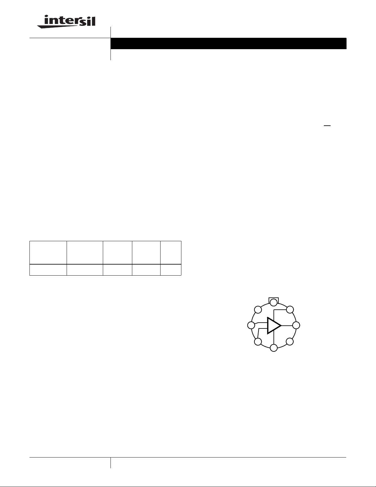
Pinout
HA-5127/883
(METAL CAN)
TOP VIEW
BAL
8
BAL
1
7
V+
1
CAUTION: These devices are sensitive to electrostatic discharge; follow proper IC Handling Procedures.
1-888-INTERSIL or 1-888-468-3774
| Intersil (and design) is a registered trademark of Intersil Americas Inc.
Copyright Intersil Americas Inc. 2001, 2004, 2005, 2006. All Rights Reserved
All other trademarks mentioned are the property of their respective owners.
2
-IN
+IN NC
-
+
3
4
V-
6
OUT
5
Page 2

HA-5127/883
www.BDTIC.com/Intersil
Absolute Maximum Ratin gs Thermal Information
Voltage Between V+ and V- Terminals . . . . . . . . . . . . . . . . . . . .44V
Differential Input Voltage (Note 2) . . . . . . . . . . . . . . . . . . . . . . . 0.7V
Voltage at Either Input Terminal . . . . . . . . . . . . . . . . . . . . . V+ to V-
Input Current . . . . . . . . . . . . . . . . . . . . . . . . . . . . . . . . . . . . . . 25mA
Differential Output Current. . . . . . . . . . . Full Short Circuit Protection
Junction Temperature (T
Storage Temperature Range. . . . . . . . . . . . . . . . . -65
ESD Rating . . . . . . . . . . . . . . . . . . . . . . . . . . . . . . . . . . . . . .<2000V
Lead Temperature (Soldering 10s) . . . . . . . . . . . . . . . . . . . .+300
CAUTION: Stresses above those listed in “Absolute Maximum Ratings” may cause permanent damage to the device. This is a stress only rating and operation of the
device at these or any other conditions above those indicated in the operational sections of this specification is not implied.
). . . . . . . . . . . . . . . . . . . . . . . . . . .+175oC
J
o
C to +150oC
o
C
Recommended Operating Conditions
Operating Temperature Range . . . . . . . . . . . . . . . -55oC to +125oC
Operating Supply Voltage. . . . . . . . . . . . . . . . . . . . . . . . . . . . . . . . ±15V
TABLE 1. DC ELECTRICAL PERFORMANCE CHARACTERISTICS
Device Tested at: V
PARAMETERS SYMBOL CONDITIONS
Input Offset Voltage V
Input Bias Current I
SUPPLY
= ±15V, R
IO
B
SOURCE
= 50Ω, R
LOAD
= 100kΩ, V
GROUP A
SUBGROUPS TEMPERATURE
VCM = 0V 1 +25oC -100 100 µV
VCM = 0V,
= 10kΩ, 50Ω
R
S
+IB+-I
---------------------------
2
B
Thermal Resistance θ
Metal Can Package . . . . . . . . . . . . . . . . . 155oC/W 67oC/W
Package Power Dissipation Limit at +75
o
C for TJ ≤ +175oC
Metal Can Package . . . . . . . . . . . . . . . . . . . . . . . . . . . . . .645mW
Package Power Dissipation Derating Factor Above +75
Metal Can Package . . . . . . . . . . . . . . . . . . . . . . . . . . . .6.5mW/
V
≤ 1/2 (V+ - V-)
INCM
R
≥ 600Ω
L
= 0V, Unless Otherwise Specified.
OUT
LIMITS
o
2, 3 +125
1+25
2, 3 +125
C, -55oC -300 300 µV
o
C - 80 nA
o
C, -55oC - 150 nA
JA
θ
JC
o
C
o
UNITSMIN MAX
C
Input Offset Current I
IO
VCM = 0V,
= 10kΩ,
+R
S
= 10kΩ
-R
S
Common Mode Range +CMR V+ = +4.7V,
V- = -25.3V
-CMR V+ = +25.3V,
V- = -4.7V
V
Large Signal Voltage
Gain
Common Mode
+CMRR ∆V
Rejection Ratio
-CMRR ∆V
Output Voltage Swing +V
-V
+V
-V
+A
-A
VOL
VOL
OUT1
OUT1
OUT2
OUT2
= 0V and +10V,
OUT
= 2kΩ
R
L
V
= 0V and -10V,
OUT
= 2kΩ
R
L
= +11V 1+25
CM
= +10V 2, 3 +125oC, -55oC 100 - dB
∆V
CM
= -11V 1+25
CM
= -10V 2, 3 +125oC, -55oC 100 - dB
∆V
CM
RL = 2kΩ 4+25
RL = 2kΩ 4+25
RL = 600Ω 4+25
RL = 600Ω 4+25
o
1+25
2, 3 +125
1+25
2, 3 +125
1+25
2, 3 +125
4+25
5, 6 +125
4+25
5, 6 +125
5, 6 +125
5, 6 +125
C -75 75 nA
o
C, -55oC -135 135 nA
o
C10.3-V
o
C, -55oC10.3 - V
o
C - -10.3 V
o
C, -55oC - -10.3 V
o
C 700 - kV/V
o
C, -55oC 300 - kV/V
o
C 700 - kV/V
o
C, -55oC 300 - kV/V
o
C 100 - dB
o
C 100 - dB
o
C11.5-V
o
C, -55oC11.5 - V
o
C--11.5V
o
C, -55oC--11.5V
o
C10-V
o
C--10V
2
FN3751.3
January 16, 2006
Page 3

HA-5127/883
www.BDTIC.com/Intersil
TABLE 1. DC ELECTRICAL PERFORMANCE CHARACTERISTICS (Continued)
Device Tested at: V
PARAMETERS SYMBOL CONDITIONS
Output Current +I
Quiescent Power
Supply Current
Power Supply
Rejection Ratio
Offset Voltage
Adjustment
NOTE:
1. Offset adjustment range is [V
2. For differential input voltages greater than 0.7V, the input current must be limited to 25mA to protect the back-to-back input diodes.
SUPPLY
= ±15V, R
SOURCE
= 50Ω, R
LOAD
= 100kΩ, V
= 0V, Unless Otherwise Specified.
OUT
GROUP A
SUBGROUPS TEMPERATURE
V
OUT
-I
OUT
+I
CC
-I
CC
+PSRR ∆V
-PSRR ∆V
= -10V 4 +25oC16.5-mA
OUT
V
= +10V 4 +25oC - -16.5 mA
OUT
V
= 0V, I
OUT
V
= 0V, I
OUT
= 14V 1 +25oC86-dB
SUP
∆V
= 13.5V 2, 3 +125oC, -55oC86 - dB
SUP
= 14V 1 +25oC86-dB
SUP
= 13.5V 2, 3 +125oC, -55oC86 - dB
∆V
SUP
= 0mA 1 +25oC-4mA
OUT
o
2, 3 +125
= 0mA 1 +25oC-4-mA
OUT
2, 3 +125
C, -55oC- 4mA
o
C, -55oC-4 - mA
+VIOAdj Note 1 1 +25oCV
o
2, 3 +125
Adj Note 1 1 +25oCV
-V
IO
2, 3 +125
(Measured) ±1mV] minimum referred to output. This test is for functionality only to assure adjustment through 0V.
IO
C, -55oCV
o
C, -55oCV
LIMITS
-1 - mV
IO
-1 - mV
IO
+1 - mV
IO
+1 - mV
IO
UNITSMIN MAX
TABLE 2. AC ELECTRICAL PERFORMANCE CHARACTERISTICS
Device Tested at: V
SUPPLY
= ±15V, R
SOURCE
= 50Ω, R
PARAMETERS SYMBOL CONDITIONS
Slew Rate +SR V
-SR V
Rise and Fall Time t
R
= -3V to +3V 7 +25oC7-V/µs
OUT
= +3V to -3V 7 +25oC7-V/µs
OUT
V
= 0 to +200mV
OUT
10% ≤ T
V
t
F
= 0 to -200mV
OUT
10% ≤ T
Overshoot +OS V
-OS V
= 0 to +200mV 7 +25oC-40%
OUT
= 0 to -200mV 7 +25oC-40%
OUT
TABLE 3. ELECTRICAL PERFORMANCE CHARACTERISTICS
Device Characterized at: V
SUPPLY
= ±15V, R
LOAD
PARAMETERS SYMBOL CONDITIONS NOTES TEMPERATURE
Average Offset Voltage Drift V
Differential Input Resistance R
TC VCM = 0V 1 -55oC to +125oC- 1.8µV/oC
IO
IN
LOAD
≤ 90%
R
≤ 90%
F
= 2kΩ, C
= 2kΩ, C
= 50pF, AV = +1V/V, Unless Otherwise Specified.
LOAD
LOAD
= 50pF, A
= +1V/V, Unless Otherwise Specified.
VCL
GROUP A
SUBGROUP TEMPERATURE
7+25
7+25
o
C - 150 ns
o
C - 150 ns
LIMITS
UNITSMIN MAX
LIMITS
MIN MAX UNITS
VCM = 0V 1 +25oC0.8-MΩ
3
FN3751.3
January 16, 2006
Page 4

Device Characterized at: V
www.BDTIC.com/Intersil
SUPPLY
HA-5127/883
TABLE 3. ELECTRICAL PERFORMANCE CHARACTERISTICS
= ±15V, R
LOAD
= 2kΩ, C
= 50pF, AV = +1V/V, Unless Otherwise Specified.
LOAD
LIMITS
PARAMETERS SYMBOL CONDITIONS NOTES TEMPERATURE
Low Frequency Peak-to-Peak
Noise
Input Noise Voltage Density E
Input Noise Current Density I
Unity Gain Bandwidth UGBW VO = 100mV 1 +25oC5-MHz
Full Power Bandwidth FPBW V
Minimum Closed Loop Stable
Gain
Settling Time t
Output Resistance R
Quiescent Power Consumption PC V
NOTES:
1. Parameters listed in Table 3 are controlled via design or process parameters and are not directly tested at final production. These parameters
are lab characterized upon initial design release, or upon design changes. These parameters are guaranteed by characterization based upon
data from multiple production runs which reflect lot to lot and within lot variation.
2. Full Power Bandwidth guarantee based on Slew Rate measurement using FPBW = Slew Rate/(2πV
3. Quiescent Power Consumption based upon Quiescent Supply Current test maximum. (No load on output.)
E
NP-P
N
N
CLSG R
S
OUT
0.1Hz to 10Hz 1 +25oC - 0.25 µV
RS = 20Ω, fO = 10Hz 1 +25oC - 10.0 nV/√Hz
RS = 20Ω, fO = 100Hz 1 +25oC-5.6nV/√Hz
RS = 20Ω, fO = 1kHz 1 +25oC-4.5nV/√Hz
RS = 2MΩ, fO = 10Hz 1 +25oC-4.0pA/√Hz
RS = 2MΩ, fO = 100Hz 1 +25oC-2.3pA/√Hz
RS = 2MΩ, fO = 1kHz 1 +25oC-0.6pA/√Hz
= 10V 1, 2 +25oC111-kHz
PEAK
= 2kΩ, CL = 50pF 1 -55oC to +125oC±1 - V/V
L
To 0.1% for a 10V Step 1 +25oC-2µs
Open Loop 1 +25oC-100Ω
OUT
= 0V, I
= 0mA 1, 3 -55oC to +125oC- 120 mW
OUT
PEAK
MIN MAX UNITS
P-P
).
TABLE 4. ELECTRICAL TEST REQUIREMENTS
MIL-STD-883 TEST REQUIREMENTS SUBGROUPS (SEE TABLES 1 AND 2) (NOTE 2)
Interim Electrical Parameters (Pre Burn-In) 1
Final Electrical Test Parameters 1 (Note 1), 2, 3, 4, 5, 6, 7
Group A Test Requirements 1, 2, 3, 4, 5, 6, 7
Groups C and D Endpoints 1
NOTES:
1. PDA applies to Subgroup 1 only.
2. The Subgroup assignments of the parameters in these tables were patterned after Mil-M-38510/135, with the exception of V
is Subgroups 1, 2, 3.
4
, which
IO
FN3751.3
January 16, 2006
Page 5

Die Characteristics
www.BDTIC.com/Intersil
SUBSTRATE POTENTIAL (Powered Up): V-
TRANSISTOR COUNT: 63
PROCESS: Bipolar Dielectric Isolation
Metallization Mask Layout
HA-5127/883
HA-5127/883
BAL
BAL
-IN
+IN
V+
OUT
V-
NC
5
FN3751.3
January 16, 2006
Page 6

Metal Can Packages (Can)
www.BDTIC.com/Intersil
HA-5127/883
HA-5127/883
REFERENCE PLANE
A
ØD ØD1
F
Q
Øb1
NOTES:
1. (All leads) Øb applies between L1 and L2. Øb1 applies between
L2 and 0.500 from the reference plane. Diameter is uncontrolled
in L1 and beyond 0.500 from the reference plane.
2. Measured from maximum diameter of the product.
α is the basic spacing from the centerline of the tab to terminal 1
3.
and β is the basic spacing of each lead or lead position (N -1
places) from
4. N is the maximum number of terminal positions.
5. Dimensioning and tolerancing per ANSI Y14.5M - 1982.
6. Controlling dimension: INCH.
α, looking at the bottom of the package.
L
L2
L1
A
A
Øe
Øb1
Øb
BASE AND
SEATING PLANE
BASE METAL LEAD FINISH
SECTION A-A
Øb2
e1
ØD2
2
β
N
1
α
k
T8.C MIL-STD-1835 MACY1-X8 (A1)
8 LEAD METAL CAN PACKAGE
INCHES MILLIMETERS
SYMBOL
A 0.165 0.185 4.19 4.70 -
Øb 0.016 0.019 0.41 0.48 1
k1
C
L
Øb1 0.016 0.021 0.41 0.53 1
Øb2 0.016 0.024 0.41 0.61 -
ØD 0.335 0.375 8.51 9.40 ØD1 0.305 0.335 7.75 8.51 ØD2 0.110 0.160 2.79 4.06 -
e 0.200 BSC 5.08 BSC -
e1 0.100 BSC 2.54 BSC -
F-0.040 - 1.02 -
k 0.027 0.034 0.69 0.86 -
k1 0.027 0.045 0.69 1.14 2
L 0.500 0.750 12.70 19.05 1
L1 - 0.050 - 1.27 1
L2 0.250 - 6.35 -1
Q 0.010 0.045 0.25 1.14 -
α
β 45
N8 84
45o BSC 45o BSC 3
o
BSC 45o BSC 3
NOTESMIN MAX MIN MAX
Rev. 0 5/18/94
All Intersil U.S. products are manufactured, assembled and tested utilizing ISO9000 quality systems.
Intersil Corporation’s quality certifications can be viewed at www.intersil.com/design/quality
Intersil products are sold by description only. Intersil Corporation reserves the right to make changes in circuit design, software and/or specifications at any time without
notice. Accordingly, the reader is cautioned to verify that data sheets are current before placing orders. Information furnished by Intersil is believed to be accurate and
reliable. However, no responsibility is assumed by Intersil or its subsidiaries for its use; nor for any infringements of patents or other rights of third parties which may result
from its use. No license is granted by implication or otherwise under any patent or patent rights of Intersil or its subsidiaries.
For information regarding Intersil Corporation and its products, see www.intersil.com
6
FN3751.3
January 16, 2006
 Loading...