

Page 1
®
www.BDTIC.com/Intersil
HA-5002/883
Data Sheet January 5, 2006
Monolithic, Wideband, High Slew Rate,
High Output Current Buffer
The HA-5002/883 is a monolithic, wideband, high slew rate,
high output current, buffer amplifier.
Utilizing the advantages of the Intersil Dielectric Isolation
technologies, the HA-5002/883 current buffer offers
1300V/µs slew rate typically and 1000V/µs minimum with
110MHz of bandwidth. The ±100mA minimum output current
capability is enhanced by a 3Ω output impedance.
The monolithic HA-5002/883 will replace the hybrid LH0002
with corresponding performance increases. These
characteristics range from the 3MΩ (typ) input impedance to
the increased output voltage swing. Monolithic design
technologies have allowed a more precise buffer to be
developed with more than an order of magnitude smaller
gain error. The voltage gain is 0.98 guaranteed minimum
with a 1kΩ load and 0.96 minimum with a 100Ω load.
The HA-5002/883 will provide many present hybrid users
with a higher degree of reliability and at the same time
increase overall circuit performance.
Ordering Information
PART
NUMBER
HA2-5002/883 HA2-5002/883 -55 to +125 8 Pin Can
HA4-5002/883 HA4-5002/883 -55 to +125 20 Ld Ceramic LCC
PAR T
MARKING
TEMP
RANGE
(°C) PACKAGE
FN3705.4
Features
• This Circuit is Processed in Accordance to MIL-STD-883
and is Fully Conformant Under the Provisions of
Paragraph 1.2.1.
• Voltage Gain (R
= 1kΩ) . . . . . . . . . . . . . . . . . . 0.98 (Min)
L
0.995 (Typ)
= 100Ω) . . . . . . . . . . . . . . . . .0.96 (Min)
(R
L
0.971 (Typ)
• High Input Impedance . . . . . . . . . . . . . . . . . . 1.5MΩ (Min)
3MΩ (Typ)
• Low Output Impedance . . . . . . . . . . . . . . . . . . . 5Ω (Max)
3Ω (Typ)
• Very High Slew Rate . . . . . . . . . . . . . . . . .1000V/µs (Min)
1300V/µs (Typ)
• Wide Small Signal Bandwidth . . . . . . . . . . .110MHz (Typ)
• High Output Current . . . . . . . . . . . . . . . . . . . .100mA (Min)
• High Pulsed Output Current . . . . . . . . . . . . . 400mA (Max)
• Monolithic Dielectric Isolation Construction
• Replaces Hybrid LH0002
Applications
• Line Driver
• Data Acquisition
• 110MHz Buffer
• High Power Current Booster
• High Power Current Source
• Sample and Holds
• Radar Cable Driver
• Video Products
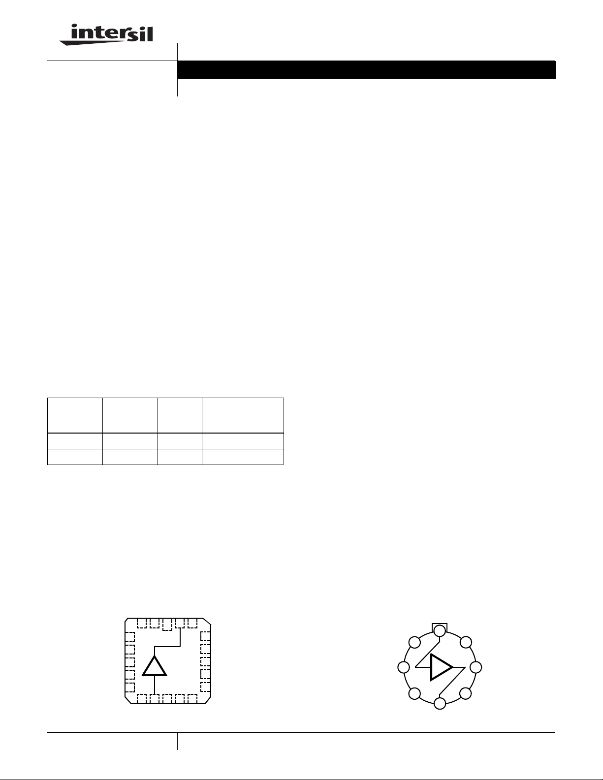
Pinouts
HA-5002/883 (CLCC)
TOP VIEW
+
1
NCNCNC
V
OUT
3 2 1 20 19
18
NC
V
NC
NC
NC
4
-
5
2
6
7
8
9101112
NC
-
IN
NC
V
1
1
NC
V2+
17
16
NC
NC
15
NC
14
13
NC
CAUTION: These devices are sensitive to electrostatic discharge; follow proper IC Handling Procedures.
1-888-INTERSIL or 1-888-468-3774
| Intersil (and design) is a registered trademark of Intersil Americas Inc.
Copyright Intersil Americas Inc. 2002, 2004-2006. All Rights Reserved
All other trademarks mentioned are the property of their respective owners.
HA-5002/883
(METAL CAN)
TOP VIEW
IN
8
V
+
1
1
2
3
NC NC
4
OUT
V
7
6
5
-
1
V2-V2+
Page 2
HA-5002/883
www.BDTIC.com/Intersil
Absolute Maximum Ratings Thermal Information
Voltage Between V+ and V- Terminals. . . . . . . . . . . . . . . . . . . . .44V
Input Voltage . . . . . . . . . . . . . . . . . . . . . . . . . . . . . Equal to Supplies
Peak Output Current (50ms On, 1s Off) . . . . . . . . . . . . . . . . . .±400mA
Junction Temperature (T
) . . . . . . . . . . . . . . . . . . . . . . . . . . . +175°C
J
Storage Temperature Range . . . . . . . . . . . . . . . . . .-65°C to +150°C
ESD Rating . . . . . . . . . . . . . . . . . . . . . . . . . . . . . . . . . . . . . .<4000V
Lead Temperature (Soldering 10s) . . . . . . . . . . . . . . . . . . . .+300°C
Operating Conditions
Operating Temperature Range . . . . . . . . . . . . . . . .-55°C to +125°C
Operating Supply Voltage. . . . . . . . . . . . . . . . . . . . . . . . . ±12V to ±15V
≥ 100Ω
R
L
CAUTION: Stresses above those listed in “Absolute Maximum Ratings” may cause permanent damage to the device. This is a stress only rating and operation of the
device at these or any other conditions above those indicated in the operational sections of this specification is not implied.
NOTE:
1. θ
is measured with the component mounted on a low effective thermal conductivity test board in free air. See Tech Brief TB379
JA
for details.
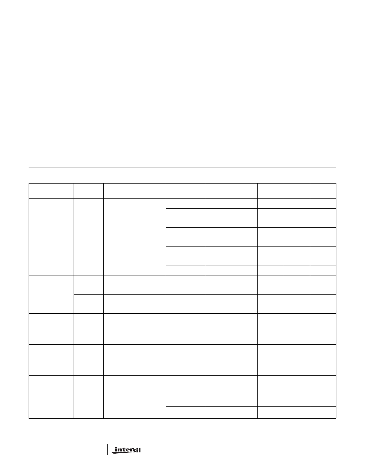
TABLE 1. DC ELECTRICAL PERFORMANCE CHARACTERISTICS
Device Tested at: V
= ±12V and ±15V, R
SUPPLY
SOURCE
PARAMETERS SYMBOL CONDITIONS
V
Input Offset
Voltage
Input Bias Current I
V
IO1
V
IO2
B1
I
B2
Voltage Gain 1 +AV
-AV
Voltage Gain 2 +AV
-AV
Voltage Gain 3 +AV
-AV
Voltage Gain 4 +AV
-AV
1
1
2
2
3
3
4
4
= ±15V 1 +25 -20 20 mV
SUP
V
= ±12V 1 +25 -20 20 mV
SUP
V
= ±15V, RS = 1kΩ 1+25-77µA
SUP
V
= ±12V, RS = 1kΩ 1+25-77µA
SUP
V
= ±12V, RL = 1kΩ,
SUP
V
= 10V
IN
V
= ±12V, RL = 1kΩ,
SUP
= -10V
V
IN
V
= ±12V, RL = 100Ω,
SUP
= 10V
V
IN
V
= ±12V, RL = 100Ω,
SUP
V
= -10V
IN
V
= ±15V, RL = 100Ω,
SUP
= 10V
V
IN
V
= ±15V, RL = 100Ω,
SUP
= -10V
V
IN
V
= ±15V,
SUP
R
= 1kΩ,
L
= +10V
V
IN
V
= ±15V,
SUP
R
= 1kΩ,
L
= -10V
V
IN
= 50Ω, C
LOAD
GROUP A
SUBGROUPS TEMPERATURE (°C) MIN MAX UNITS
Thermal Resistance θ
(°C/W) θJC (°C/W)
JA
Metal Can Package . . . . . . . . . . . . . . . 160 70
Ceramic LCC Package. . . . . . . . . . . . . 80 30
Package Power Dissipation Limit at +75°C for T
Metal Can Package . . . . . . . . . . . . . . . . . . . . . . . . . . . . . .625mW
≤ +175°C
J
Ceramic LCC Package. . . . . . . . . . . . . . . . . . . . . . . . . . . . . 1.25W
Package Power Dissipation Derating Factor Above +75°C
Metal Can Package . . . . . . . . . . . . . . . . . . . . . . . . . . . .6.3mW/°C
Ceramic LCC Package. . . . . . . . . . . . . . . . . . . . . . . . . 12.5mW/°C
≤ 10pF, VIN = 0V, Unless Otherwise Specified.
2, 3 +125, -55 -30 30 mV
2, 3 +125, -55 -30 30 mV
2, 3 +125, -55 -10 10 µA
2, 3 +125, -55 -10 10 µA
1 +25 0.98 - V/V
2, 3 +125, -55 0.98 - V/V
1 +25 0.98 - V/V
2, 3 +125, -55 0.98 - V/V
1 +25 0.96 - V/V
1 +25 0.96 - V/V
1 +25 0.96 - V/V
1 +25 0.96 - V/V
1 +25 0.99 - V/V
2, 3 +125, -55 0.99 - V/V
1 +25 0.99 - V/V
2, 3 +125, -55 0.99 - V/V
2
FN3705.4
January 5, 2006
Page 3
HA-5002/883
www.BDTIC.com/Intersil
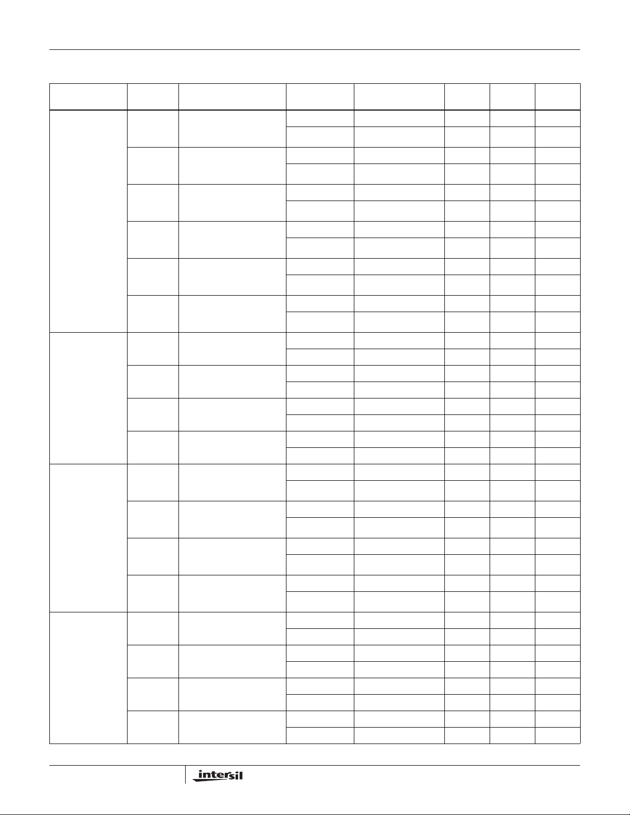
Device Tested at: V
= ±12V and ±15V, R
SUPPLY
SOURCE
PARAMETERS SYMBOL CONDITIONS
TABLE 1. DC ELECTRICAL PERFORMANCE CHARACTERISTICS (Continued)
Output Voltage
Swing
Output Current +I
Power Supply
Rejection Ratio
+V
OUT1VSUP
-V
OUT1
+V
OUT2VSUP
-V
OUT2
+V
OUT3VSUP
-V
OUT3
OUT1
-I
OUT1
+I
OUT2
-I
OUT2
+PSRR
1
= ±15V,
= 100Ω,
R
L
= +15V
V
IN
V
= ±15V,
SUP
= 100Ω,
R
L
= -15V
V
IN
= ±15V,
= 1kΩ,
R
L
= +15V
V
IN
V
= ±15V,
SUP
= 1kΩ,
R
L
= -15V
V
IN
= ±12V,
= 1kΩ,
R
L
= +12V
V
IN
V
= ±12V,
SUP
= 1kΩ,
R
L
= -12V
V
IN
V
= ±15V,
SUP
V
= +10V
OUT
V
= ±15V,
SUP
= -10V
V
OUT
V
= ±12V,
SUP
= +10V
V
OUT
V
= ±12V,
SUP
V
= -10V
OUT
∆V
= ±5V,
SUP
V+ = +20V, V- = -15V,
V+ = +10V, V- = -15V
∆V
-PSRR
1
SUP
= ±5V,
V+ = +15V, V- = -20V,
V+ = +15V, V- = -10V
∆V
+PSRR
2
SUP
= ±5V,
V+ = +17V, V- = -12V,
V+ = +7V, V- = -12V
∆V
-PSRR
2
SUP
= ±5V,
V+ = +12V, V- = -17V,
V+ = +12V, V- = -7V
V
V
V
V
V
V
V
V
SUP
OUT
SUP
OUT
SUP
OUT
SUP
OUT
= ±15V,
= 0V
= ±15V,
= 0V
= ±12V,
= 0V
= ±12V,
= 0V
Power Supply
Current
+ICC
-ICC
+ICC
-ICC
1
1
2
2
= 50Ω, C
≤ 10pF, VIN = 0V, Unless Otherwise Specified.
LOAD
GROUP A
SUBGROUPS TEMPERATURE (°C) MIN MAX UNITS
1 +25 10 - V
2, 3 +125, -55 10 - V
1 +25 - -10 V
2, 3 +125, -55 - -10 V
1 +25 10 - V
2, 3 +125, -55 10 - V
1 +25 - -10 V
2, 3 +125, -55 - -10 V
1 +25 10 - V
2, 3 +125, -55 10 - V
1 +25 - -10 V
2, 3 +125, -55 - -10 V
1 +25 100 - mA
2, 3 +125, -55 100 - mA
1 +25 - -100 mA
2, 3 +125, -55 - -100 mA
1 +25 100 - mA
2, 3 +125, -55 100 - mA
1 +25 - -100 mA
2, 3 +125, -55 - -100 mA
1 +25 54 - dB
2, 3 +125, -55 54 - dB
1 +25 54 - dB
2, 3 +125, -55 54 - dB
1 +25 54 - dB
2, 3 +125, -55 54 - dB
1 +25 54 - dB
2, 3 +125, -55 54 - dB
1+25-10mA
2, 3 +125, -55 - 10 mA
1+25-10-mA
2, 3 +125, -55 -10 - mA
1+25-10mA
2, 3 +125, -55 - 10 mA
1+25-10-mA
2, 3 +125, -55 -10 - mA
3
FN3705.4
January 5, 2006
Page 4
HA-5002/883
www.BDTIC.com/Intersil
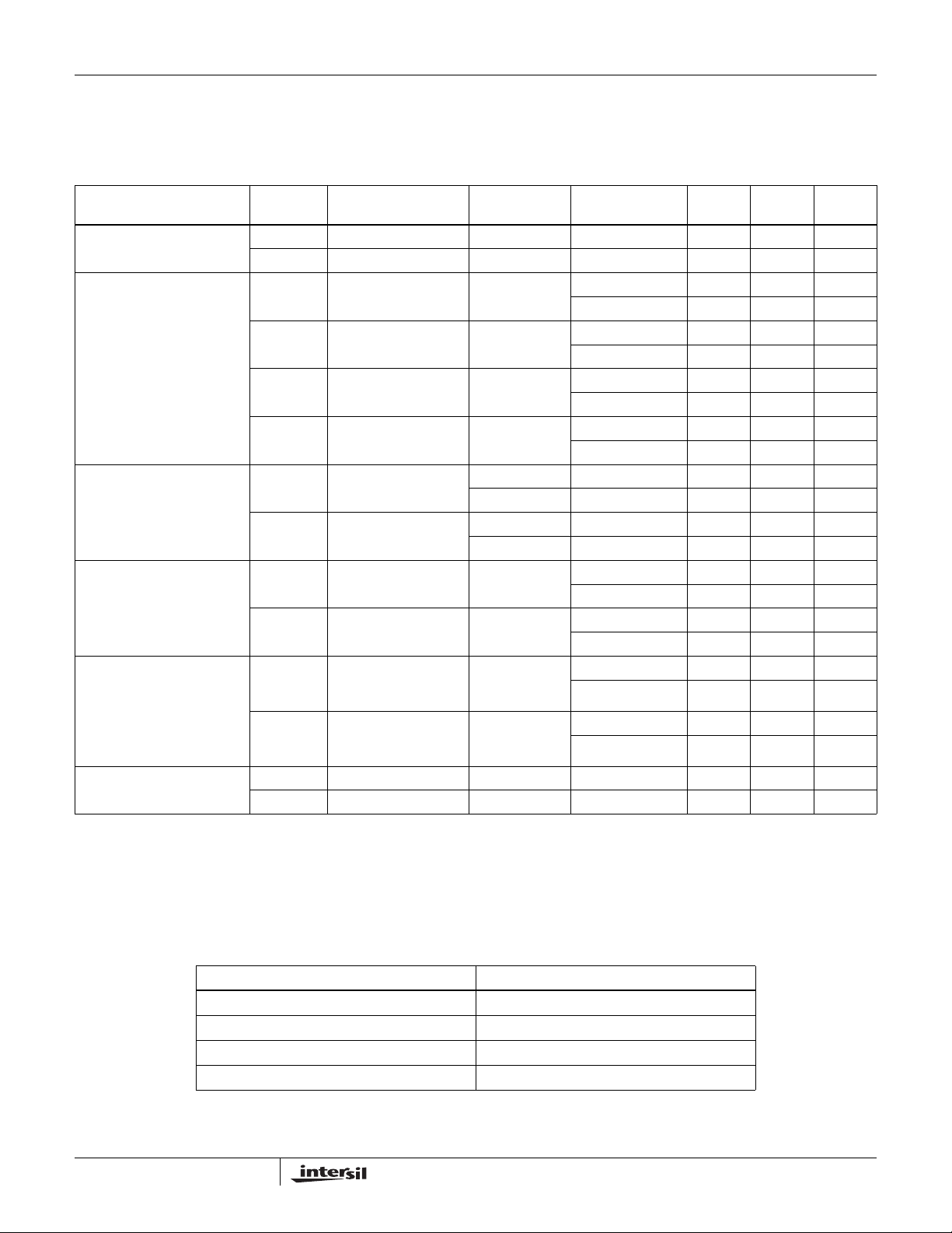
TABLE 2. AC ELECTRICAL PERFORMANCE CHARACTERISTICS
Table 2 Intentionally Left Blank. See AC Specifications in Table 3
TABLE 3. ELECTRICAL PERFORMANCE CHARACTERISTICS
Device Characterized at: V
= ±15V or ±12V, R
SUPPLY
PARAMETERS SYMBOL CONDITIONS NOTES
Input Resistance R
IN1
R
IN2
Slew Rate +SR
-SR
+SR
-SR
Rise and Fall Time T
T
Overshoot +OS V
-OS V
Quiescent Power
PC
Consumption
PC
Output Resistance R
OUT1
R
OUT2
V
SUP
V
SUP
V
1
SUP
V
OUT
V
1
SUP
V
OUT
V
2
SUP
V
OUT
V
2
SUP
V
OUT
V
R
F
SUP
V
OUT
V
SUP
V
OUT
SUP
V
OUT
SUP
V
OUT
V
1
SUP
V
= 0V,
IN
I
OUT
V
2
SUP
V
= 0V,
IN
I
OUT
V
SUP
V
SUP
NOTES:
1. Parameters listed in Table 3 are controlled via design or process parameters and are not directly tested at final production. These parameters
are lab characterized upon initial design release, or upon design changes. These parameters are guaranteed by characterization based upon
data from multiple production runs which reflect lot to lot and within lot variation.
2. Measured between 10% and 90% points.
3. Quiescent Power Consumption based upon Quiescent Supply Current test maximum. (No load on outputs.)
LOAD
= 1kΩ, C
≤ 10pF, Unless Otherwise Specified.
LOAD
TEMPERATURE
(°C) MIN MAX UNITS
= ±15V 1 +25 1.5 - MΩ
= ±12V 1 +25 1.5 - MΩ
= ±15V,
= -5V to +5V
= ±15V,
= +5V to -5V
= ±12V,
= -5V to +5V
= ±12V,
= +5V to -5V
= ±15V or ±12V,
= 0 to +500mV
= ±15V or ±12V,
= 0 to -500mV
= ±12V or ±15V,
= 0 to +500mV
= ±12V or ±15V,
= 0 to -500mV
= ±15V,
= 0mA
= ±12V,
= 0mA
1 +25 1000 - V/µs
+125, -55 1000 - V/µs
1 +25 1000 - V/µs
+125, -55 1000 - V/µs
1 +25 1000 - V/µs
+125, -55 1000 - V/µs
1 +25 1000 - V/µs
+125, -55 1000 - V/µs
1, 2 +25 - 10 ns
1, 2 +125, -55 - 10 ns
1, 2 +25 - 10 ns
1, 2 +125, -55 - 10 ns
1+25-30%
+125, -55 - 30 %
1+25-30%
+125, -55 - 30 %
1, 3 +25 - 300 mW
+125, -55 - 300 mW
1, 3 +25 - 240 mW
+125, -55 - 240 mW
= ±12V 1 +25 - 5 Ω
= ±12V 1 +25 - 5 Ω
TABLE 4. ELECTRICAL TEST REQUIREMENTS
MIL-STD-883 TEST REQUIREMENTS SUBGROUPS (SEE TABLE 1)
Interim Electrical Parameters (Pre Burn-In) 1
Final Electrical Test Parameters 1 (Note 1), 2, 3
Group A Test Requirements 1, 2, 3
Groups C and D Endpoints 1
NOTE:
1. PDA applies to Subgroup 1 only.
4
FN3705.4
January 5, 2006
Page 5
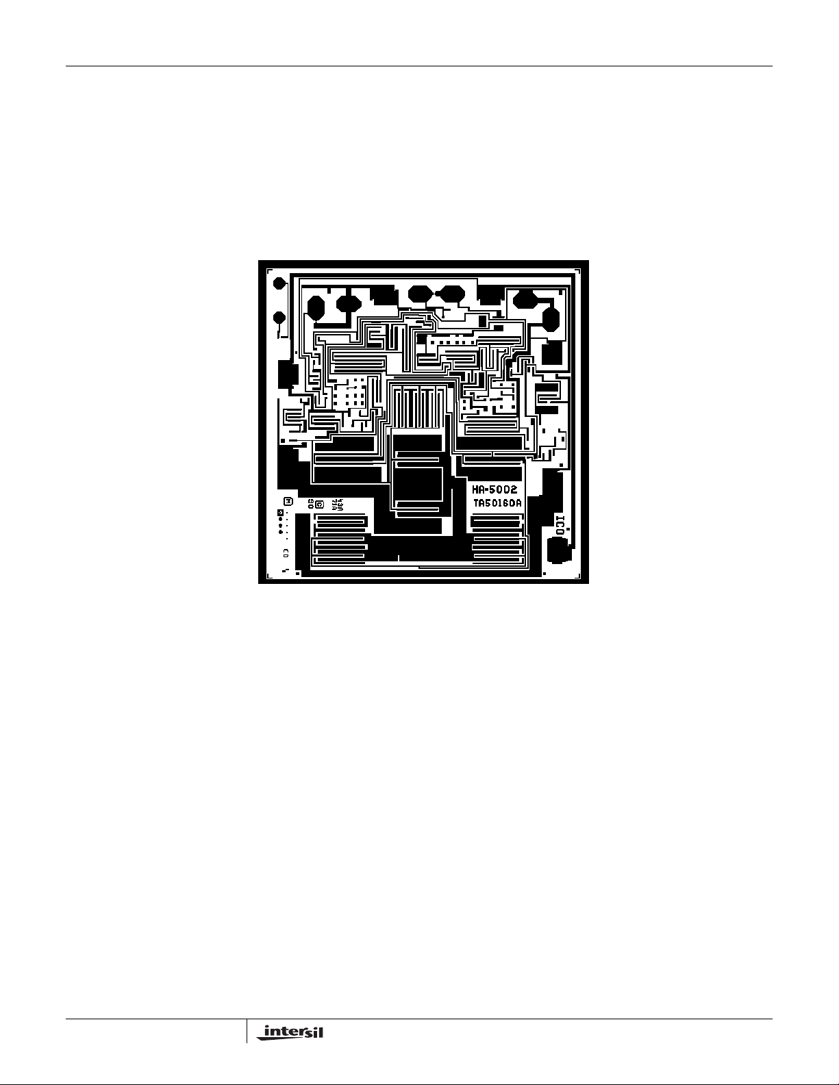
Die Characteristics
www.BDTIC.com/Intersil
SUBSTRATE POTENTIAL (POWERED UP): V1-
TRANSISTOR COUNT: 27
PROCESS: Bipolar Dielectric Isolation
Metallization Mask Layout
HA-5002/883
HA-5002/883
V
1
+ (ALT)
V2+
V1-
OUT
IN
V1- (ALT)
V
-
2
+
V
1
5
FN3705.4
January 5, 2006
Page 6
HA-5002/883
www.BDTIC.com/Intersil
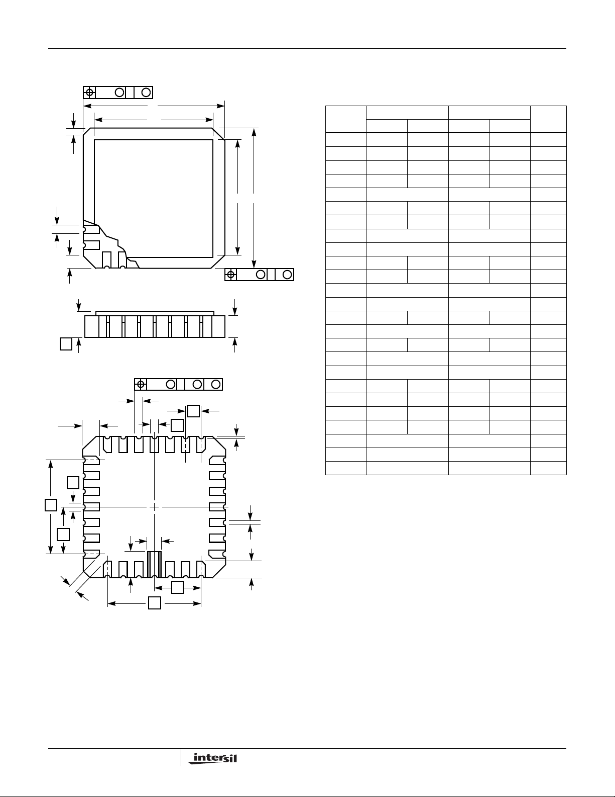
Ceramic Leadless Chip Carrier Packages (CLCC)
j x 45
E1
o
B
h x 45
-E-
E2
e1
o
A
-F-
0.010 E HS S
L
D
D3
0.007 E FM S HS
B1
L2
D1
-H-
D2
B2
J20.A MIL-STD-1835 CQCC1-N20 (C-2)
20 PAD CERAMIC LEADLESS CHIP CARRIER PACKAGE
INCHES MILLIMETERS
SYMBOL
A 0.060 0.100 1.52 2.54 6, 7
A1 0.050 0.088 1.27 2.23 -
B-----
B1 0.022 0.028 0.56 0.71 2, 4
E
E3
0.010 E FSS
A1
PLANE 2
PLANE 1
e
L3
B3
L1
B2 0.072 REF 1.83 REF B3 0.006 0.022 0.15 0.56 -
D 0.342 0.358 8.69 9.09 D1 0.200 BSC 5.08 BSC D2 0.100 BSC 2.54 BSC D3 -0.358-9.092
E 0.342 0.358 8.69 9.09 E1 0.200 BSC 5.08 BSC E2 0.100 BSC 2.54 BSC E3 -0.358-9.092
e 0.050 BSC 1.27 BSC e1 0.015 - 0.38 - 2
h 0.040 REF 1.02 REF 5
j 0.020 REF 0.51 REF 5
L 0.045 0.055 1.14 1.40 L1 0.045 0.055 1.14 1.40 L2 0.075 0.095 1.91 2.41 L3 0.003 0.015 0.08 0.38 -
ND 5 5 3
NE 5 5 3
N20 203
NOTES:
1. Metallized castellations shall be connected to plane 1 terminals
and extend toward plane 2 across at least two layers of ceramic
or completely across all of the ceramic layers to make electrical
connection with the optional plane 2 terminals.
2. Unless otherwise specified, a minimum clearance of 0.015 inch
(0.38mm) shall be maintained between all metallized features
(e.g., lid, castellations, terminals, thermal pads, etc.)
3. Symbol “N” is the maximum number of terminals. Symbols “ND”
and “NE” are the number of terminals along the sides of length
“D” and “E”, respectively.
4. The required plane 1 terminals and optional plane 2 terminals (if
used) shall be electrically connected.
5. The corner shape (square, notch, radius, etc.) may vary at the
manufacturer’s option, from that shown on the drawing.
6. Chip carriers shall be constructed of a minimum of two ceramic
layers.
7. Dimension “A” controls the overall package thickness. The maximum “A” dimension is package height before being solder dipped.
8. Dimensioning and tolerancing per ANSI Y14.5M-1982.
9. Controlling dimension: INCH.
NOTESMIN MAX MIN MAX
Rev. 0 5/18/94
6
FN3705.4
January 5, 2006
Page 7
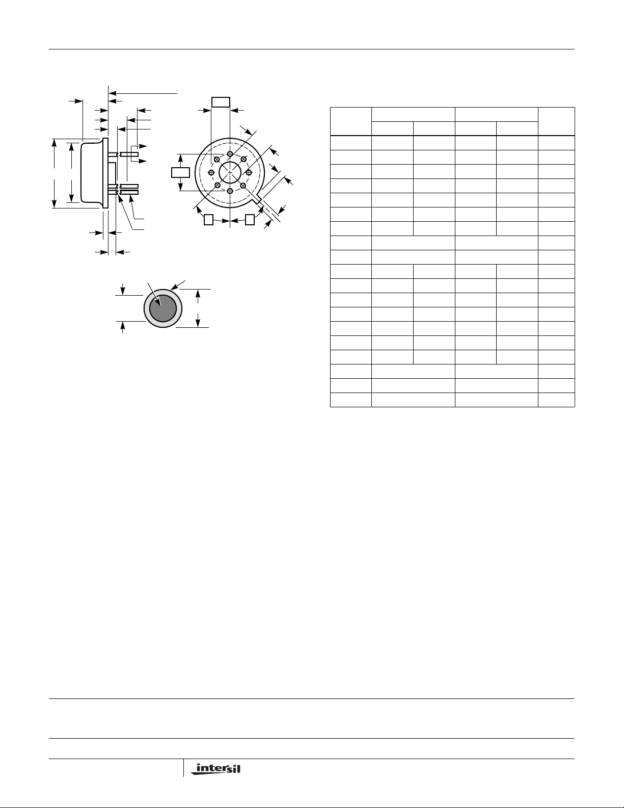
Metal Can Packages (Can)
www.BDTIC.com/Intersil
HA-5002/883
REFERENCE PLANE
A
ØD ØD1
F
Q
Øb1
NOTES:
1. (All leads) Øb applies between L1 and L2. Øb1 applies between
L2 and 0.500 from the reference plane. Diameter is uncontrolled
in L1 and beyond 0.500 from the reference plane.
2. Measured from maximum diameter of the product.
α is the basic spacing from the centerline of the tab to terminal 1
3.
and β is the basic spacing of each lead or lead position (N -1
places) from
4. N is the maximum number of terminal positions.
5. Dimensioning and tolerancing per ANSI Y14.5M - 1982.
6. Controlling dimension: INCH.
α, looking at the bottom of the package.
L
L2
L1
A
A
Øe
Øb1
Øb
BASE AND
SEATING PLANE
BASE METAL LEAD FINISH
SECTION A-A
Øb2
e1
ØD2
2
β
N
1
α
k
T8.C MIL-STD-1835 MACY1-X8 (A1)
8 LEAD METAL CAN PACKAGE
INCHES MILLIMETERS
SYMBOL
A 0.165 0.185 4.19 4.70 -
Øb 0.016 0.019 0.41 0.48 1
k1
C
L
Øb1 0.016 0.021 0.41 0.53 1
Øb2 0.016 0.024 0.41 0.61 -
ØD 0.335 0.375 8.51 9.40 ØD1 0.305 0.335 7.75 8.51 ØD2 0.110 0.160 2.79 4.06 -
e 0.200 BSC 5.08 BSC -
e1 0.100 BSC 2.54 BSC -
F - 0.040 - 1.02 k 0.027 0.034 0.69 0.86 -
k1 0.027 0.045 0.69 1.14 2
L 0.500 0.750 12.70 19.05 1
L1 - 0.050 - 1.27 1
L2 0.250 - 6.35 - 1
Q 0.010 0.045 0.25 1.14 -
α
β 45
N8 84
45o BSC 45o BSC 3
o
BSC 45o BSC 3
NOTESMIN MAX MIN MAX
Rev. 0 5/18/94
All Intersil U.S. products are manufactured, assembled and tested utilizing ISO9000 quality systems.
Intersil Corporation’s quality certifications can be viewed at www.intersil.com/design/quality
Intersil products are sold by description only. Intersil Corporation reserves the right to make changes in circuit design, software and/or specifications at any time without
notice. Accordingly, the reader is cautioned to verify that data sheets are current before placing orders. Information furnished by Intersil is believed to be accurate and
reliable. However, no responsibility is assumed by Intersil or its subsidiaries for its use; nor for any infringements of patents or other rights of third parties which may result
from its use. No license is granted by implication or otherwise under any patent or patent rights of Intersil or its subsidiaries.
For information regarding Intersil Corporation and its products, see www.intersil.com
7
FN3705.4
January 5, 2006
 Loading...