

Data Sheet No. PD60299
IRS212(7, 71, 8, 81)(S)PbF
CURRENT SENSING SINGLE CHANNEL DRIVER
Features
Product Summary
• Floating channel designed for bootstrap operation
Fully operational to +600 V
Tolerant to negative transient voltage dV/dt immune
• Application-specific gate drive range:
Motor Drive: 12 V to 20 V (IRS2127/IRS2128)
Automotive: 9 V to 20 V (IRS21271/IRS21281)
• Undervoltage lockout
• 3.3 V, 5 V, and 15 V input logic compatible
IO+/- 200 mA / 420 mA
V
V
OFFSET
12 V - 20V 9 V - 20 V
OUT
600 V max.
(IRS2127/IR2128) (IRS21271/IR21281)
• FAULT lead indicates shutdown has occured
• Output in phase with input (IRS2127/IRS21271)
V
CSth
250 mV or 1.8 V
• Output out of phase with input (IRS2128/IRS21281)
• RoHS compliant
t
on/off
(typ.) 150 ns & 150 ns
Description
The IRS2127/IRS2128/IRS21271/IRS21281 are
high voltage, high speed power MOSFET and IGBT
drivers. Proprietary HVIC and latch immune CMOS
technologies enable ruggedized monolithic construction. The logic input is compatible with standard
CMOS or LSTTL outputs, down to 3.3 V. The protection circuity detects over-current in the driven power
transistor and terminates the gate drive voltage. An
open drain
FAULT
signal is provided to indicate that
an over-current shutdown has occurred. The output
driver features a high pulse current buffer stage designed for minimum cross-conduction. The floating channel can be used to drive an N-channel power MOSFET or IGBT in the high-side or low-side configuration which
operates up to 600 V.
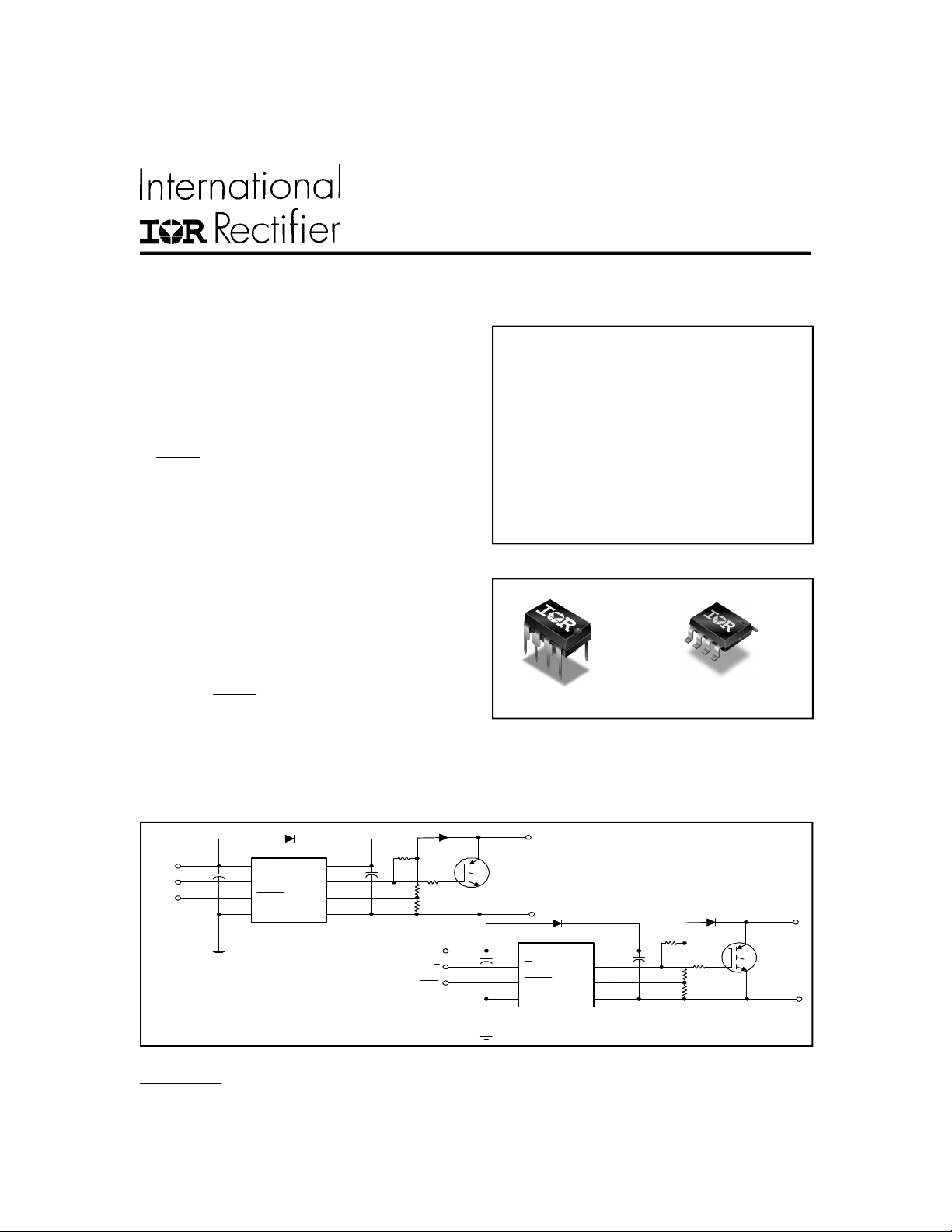
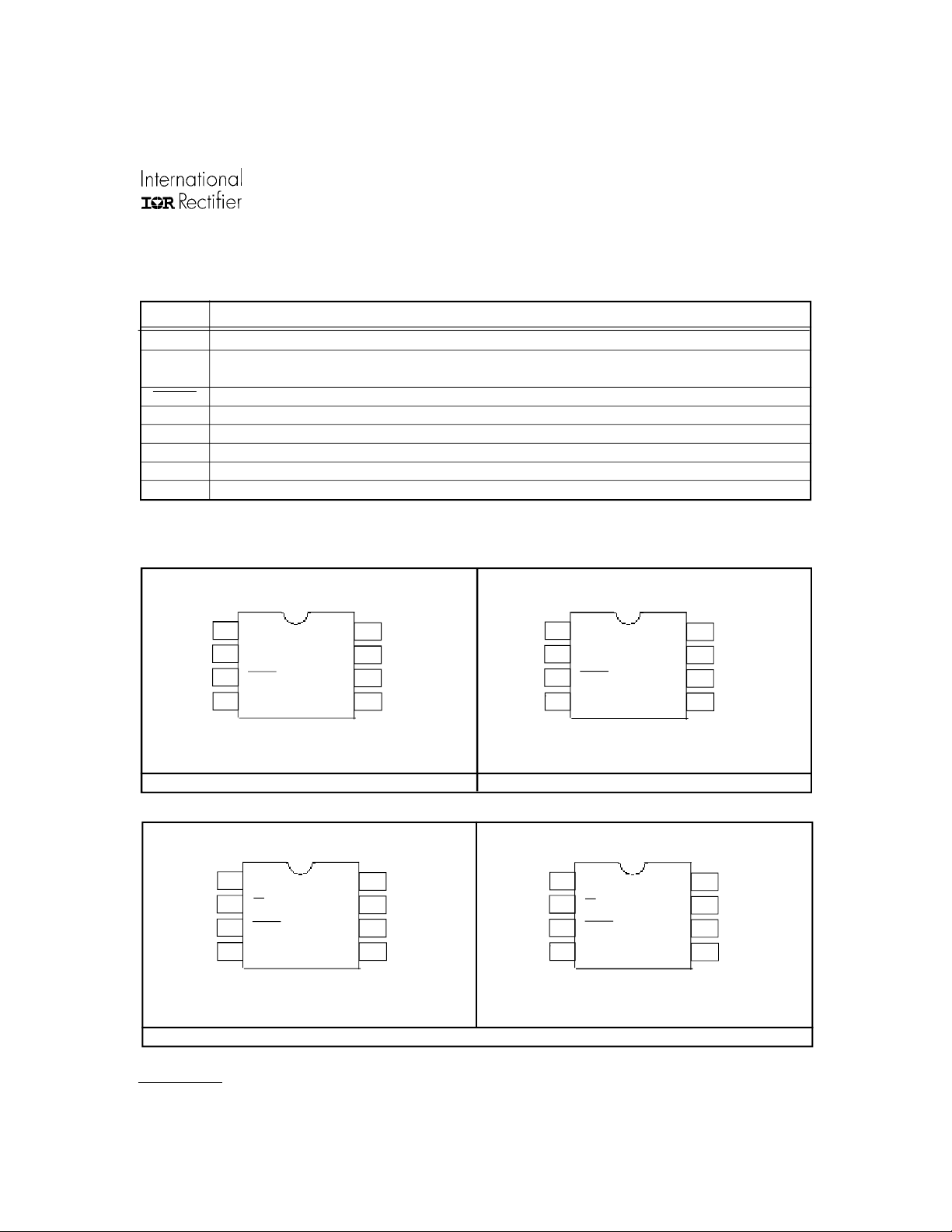
Packages
8-Lead PDIP 8-Lead SOIC
Typical Connection
V
CC
IN
FAULT
(Refer to Lead Assignments for correct pin configuration).
These diagrams show electrical connections only. Please
refer to our Application Notes and DesignTips for proper
circuit board layout.
www.irf.com 1
V
CC
IN
FAULT
COM
HO
V
B
CS
V
S
IRS2127/IRS21271
FAULT
V
CC
IN
V
CC
IN
FAULT
COM
HO
V
B
CS
V
S
IRS2128/IRS21281
IRS212(7, 71, 8, 81)(S)PbF
Absolute Maximum Ratings
Absolute maximum ratings indicate sustained limits beyond which damage to the device may occur. All voltage parameters are absolute voltages referenced to COM. The thermal resistance and power dissipation ratings are measured
under board mounted and still air conditions.
Symbol Definition Min. Max. Units
V
B
V
S
V
HO
V
CC
V
IN
V
FLT
V
CS
dVs/dt Allowable offset supply voltage transient — 50 V/ns
P
D
Rth
JA
T
J
T
S
T
L
High-side floating supply voltage -0.3 625
High-side floating offset voltage VB - 25 VB + 0.3
High-side floating output voltage VS - 0.3 V
+ 0.3
B
Logic supply voltage -0.3 25 V
Logic input voltage -0.3 V
FAULT output voltage -0.3 V
Current sense voltage VS - 0.3 V
Package power dissipation @ TA ≤ +25 °C
Thermal resistance, junction to ambient
8-Lead DIP — 1.0
8-Lead SOIC — 0.625
8-Lead DIP — 125
8-Lead SOIC — 200
CC
CC
B
+ 0.3
+ 0.3
+ 0.3
W
°C/W
Junction temperature — 150
Storage temperature -55 150
°C
Lead temperature (soldering, 10 seconds) — 300
Recommended Operating Conditions
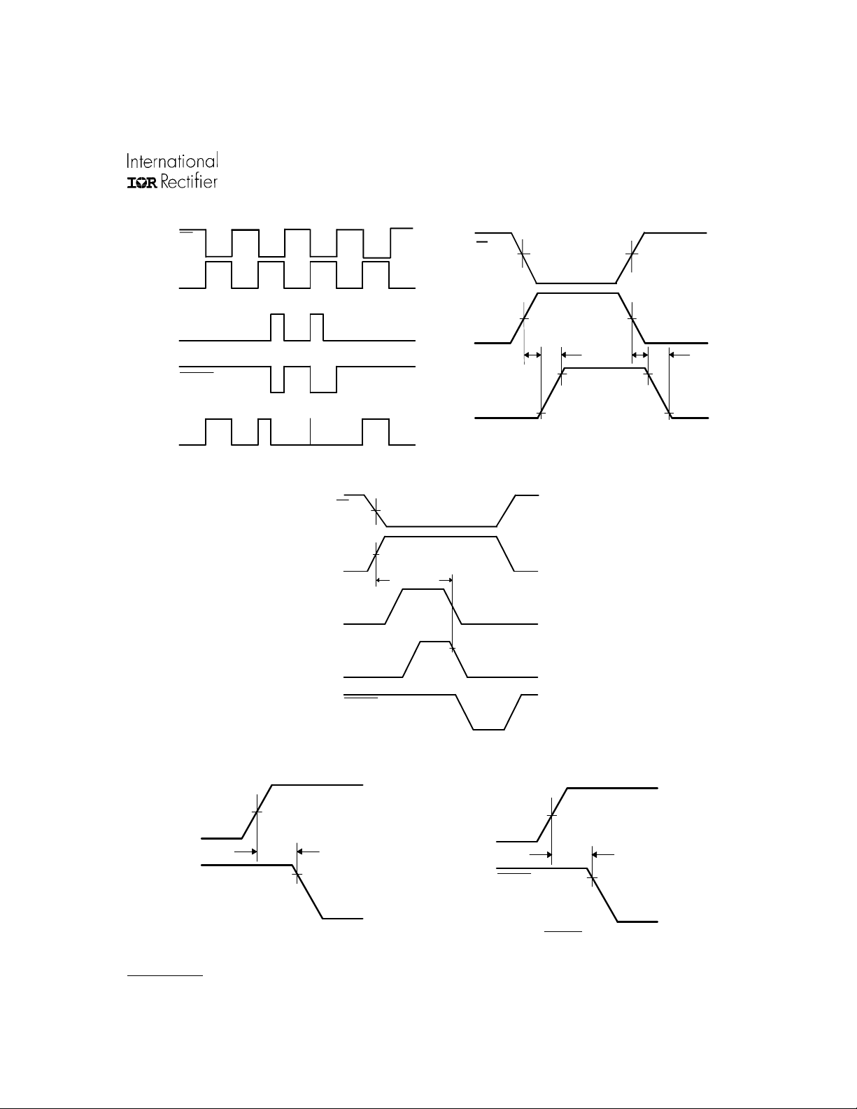
The input/output logic timing diagram is shown in Fig. 1. For proper operation the device should be used within the
recommended conditions. The VS offset rating is tested with all supplies biased at 15 V differential.
Symbol Definition Min. Max. Units
V
B
V
S
V
HO
V
CC
V
IN
V
FLT
V
CS
T
A
High-side floating supply voltage
(IRS21271/IRS21281) VS + 9 VS + 20
High-side floating offset voltage Note 1 600
High-side floating output voltage V
Logic supply voltage 10 20
Logic input voltage 0 V
FAULT output voltage 0 V
Current sense signal voltage V
Ambient temperature -40 125 °C
Note 1: Logic operational for VS of -5 V to +600 V. Logic state held for VS of -5 V to -VBS. (Please refer to the Design Tip
DT97-3 for more details).
www.irf.com 2
(IRS2127/IRS2128) VS + 12 VS + 20
S
S
V
B
CC
CC
V
+ 5
S
V
IRS212(7, 71, 8, 81)(S)PbF
Dynamic Electrical Characteristics
V
(VCC, VBS) = 15 V, CL = 1000 pF and TA = 25 °C unless otherwise specified. The dynamic electrical characteristics
BIAS
are measured using the test circuit shown in Fig. 3.
Symbol Definition Min. Typ.Max.Units Test Conditions
t
on
t
off
t
t
t
bl
t
cs
t
flt
Turn-on propagation delay — 150 200 V
Turn-off propagation delay — 150 200 V
Turn-on rise time — 80 130
r
Turn-off fall time — 40 65 ns
f
Start-up blanking time 550 750 950
CS shutdown propagation delay — 65 360
CS to FAULT pull-up propagation delay — 270 510
= 0 V
S
= 600 V
S
Static Electrical Characteristics
V
BIAS (VCC
COM. The VO and IO parameters are referenced to VS.
Symbol Definition Min. Typ.Max.Units Test Conditions
V
V
V
R
, VBS) = 15 V and TA = 25 °C unless otherwise specified. The VIN, V
V
V
CSTH+
V
OH
V
OL
I
LK
I
QBS
I
QCC
I
IN+
I
IN-
I
CS+
I
CS-
BSUV+
BSUV-
I
O+
I
O-
on,FLT
Logic “1” input voltage (IRS2127/IRS21271)
IH
Logic “0” input voltage (IRS2128/IRS21281)
Logic “0” input voltage (IRS2127/IRS21271)
IL
Logic “1” input voltage (IRS2128/IRS21281)
CS input positive (IRS2127/IRS2128) 180 250 320 mV
going threshold
High level output voltage, V
Low level output voltage, V
(IRS21271/IRS21281)
- V
BIAS
O
O
Offset supply leakage current — — 50 VB = VS = 600 V
Quiescent V
supply current — 300 800
BS
Quiescent VCC supply current — 60 120
Logic “1” input bias current — 7.0 15
Logic “0” input bias current — — 5.0 V
“High” CS bias current — — 5.0 V
“High” CS bias current — — 5.0 V
V
supply undervoltage (IRS2127/IRS2128) 8.8 10.3 11.8
BS
positive going threshold (IRS21271/IRS21281) 6.3 7.2 8.2
V
supply undervoltage
BS
negative going
threshold
(IRS2127/IRS2128)
(IRS21271/IRS21281) 6.0 6.8 7.7
Output high short circuit pulsed current 200 290 —
Output low short circuit pulsed current 420 600 —
FAULT - low on resistance — 125 — Ω
2.5
1.5 1.8 2.1
— 0.05 0.2
— 0.02 0.1
7.5 9.0 10.6
TH,
—
— — 0.8
and IIN parameters are referenced to
—
V
VCC = 10 V to 20 V
V
IO = 2 mA
VIN = 0 V or 5 V
µA
VIN = 5 V
= 0 V
IN
= 3 V
CS
= 0 V
CS
V
VO = 0 V, V
mA
VO = 15 V, V
IN
PW ≤ 10 µs
IN
PW ≤ 10 µs
= 5 V
= 0 V
www.irf.com 3
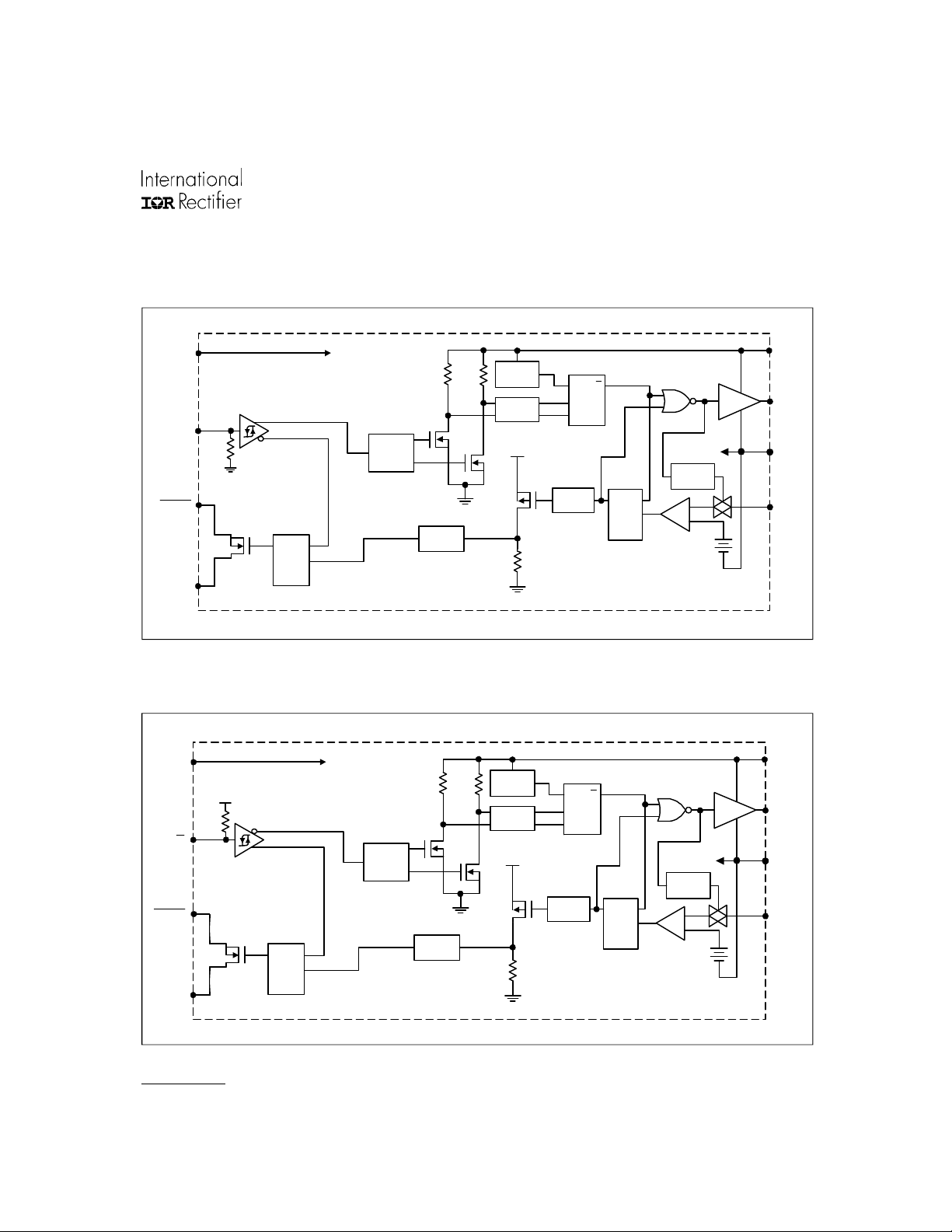
Functional Block Diagram IRS2127/IRS21271
IRS212(7, 71, 8, 81)(S)PbF
V
CC
HV
UP
SHIFTERS
LEVEL
SHIFT
UV
DETECT
PULSE
FILTER
IN
FAULT
Q R
PULSE
GEN
PULSE
FILTER
DOWN
SHIFTER
V
B
S
COM
Functional Block Diagram IRS2128/IRS21281
V
FAULT
COM
CC
5V
UP
SHIFTERS
HV
LEVEL
SHIFT
IN
PULSE
GEN
PULSE
Q
R
FILTER
S
DETECT
PULSE
FILTER
DOWN
SHIFTER
UV
V
B
R Q
R
S
PULSE
GEN
R Q
R
S
PULSE
GEN
Q R
Q
V
B
BUFFER
HO
V
S
DELAY
S
-
+
BUFFER
V
HO
V
CS
B
S
DELAY
R
S
-
CS
+
www.irf.com 4
Lead Definitions
Symbol Description
V
CC
IN
FAULT
Logic and gate drive supply
Logic input for gate driver output (HO), in phase with HO (IRS2127/IRS21271)
out of phase with HO (IRS2128/IRS21281)
Indicates over-current shutdown has occurred, negative logic
COM Logic ground
V
HO
V
CS
High-side floating supply
B
High-side gate drive output
High-side floating supply return
S
Current sense input to current sense comparator
Lead Assignments
IRS212(7, 71, 8, 81)(S)PbF
1
V
CC
2
I N
3
FAULT
4
COM
V
HO
C
V
1
8
B
7
6
S
5
S
V
CC
2
I N
3
FAULT
4
COM
HO
V
8
B
7
C
6
S
V
5
S
8 Lead PDIP 8 Lead SOIC
IRS2127/IRS21271 IRS2127S/IRS21271S
1
V
CC
2
I N
3
FAULT
4
COM
V
HO
C
V
8
B
7
6
S
5
S
1
2
3
4
8 Lead PDIP 8 Lead SOIC
V
CC
I N
FAULT
COM
V
HO
C
V
8
B
7
6
S
5
S
IRS2128/IRS21281 IRS2128S/IRS21281S
www.irf.com 5
IRS212(7, 71, 8, 81)(S)PbF
IN
(IRS2128/
IRS21281)
IN
(IRS2127/
IRS21271)
CS
FAULT
HO
Figure 1. Input/Output Timing Diagram
IN
(IRS2128/
IRS21281)
IN
(IRS2127/
IRS21271)
CS
HO
50%
50%
t
bl
IN
(IRS2128/
50% 50%
IRS21281)
50%
IN
(IRS2127/
IRS21271)
HO
t
t
r
on
10% 10%
Figure 2. Switching Time Waveform Definition
90%
50%
t
off
90% 90%
t
f
FAULT
Figure 3. Start-Up Blanking Time Waveform
Definitions
V
CSTH
CS
t
cs
HO
90%
Figure 4. CS Shutdown Waveform Definitions
CS
FAULT
Figure 5. CS to
V
CSTH
t
flt
90%
Waveform Definitions
FAULT
www.irf.com 6
IRS212(7, 71, 8, 81)(S)PbF
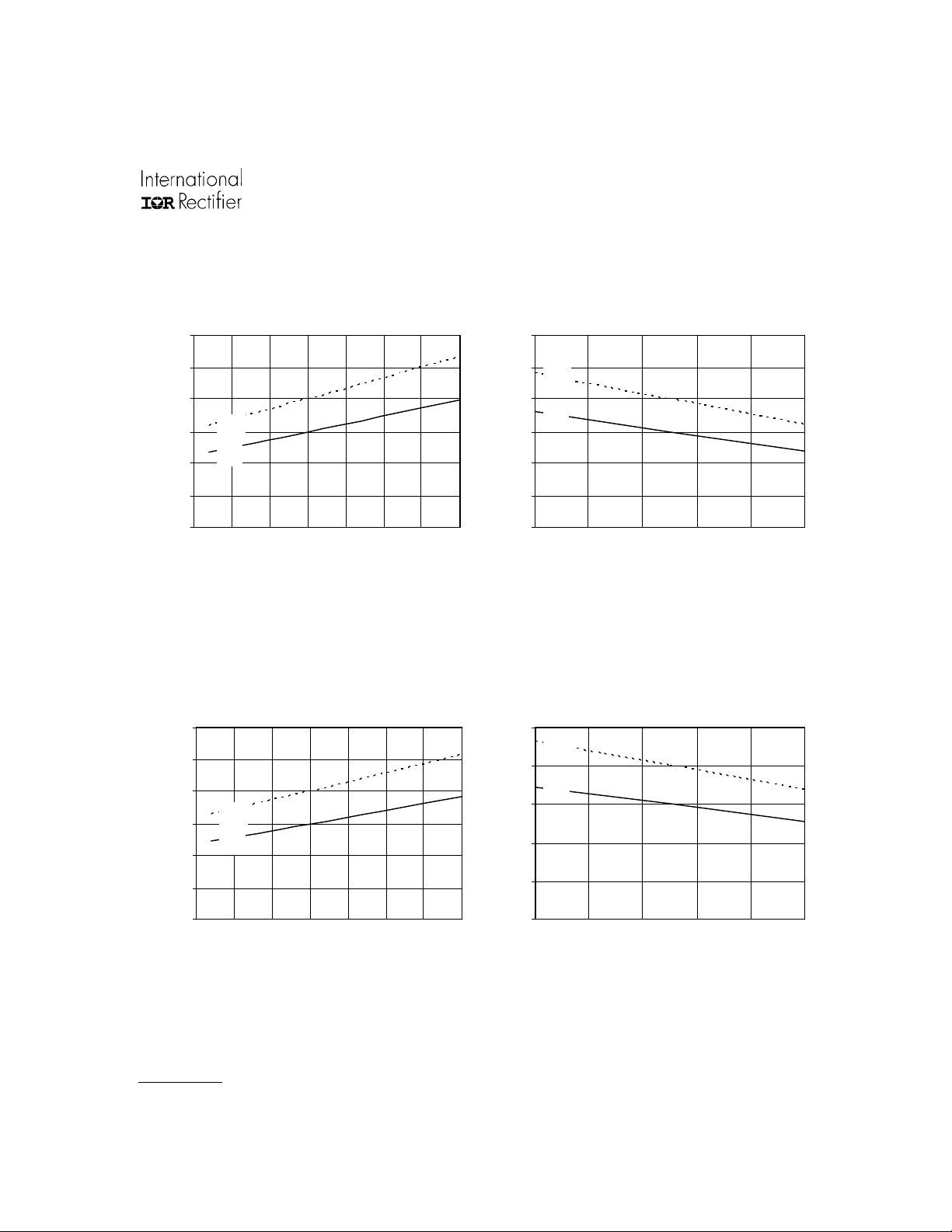
Turn-Off Delay Ti me (ns)
T ur n- On D elay T ime ( ns )
T ur n- On D elay T ime ( ns )
Turn-Off Delay Ti me (ns)
Temperature
Temperature
300
250
200
150
100
50
300
250
200
150
100
Max
Typ
0
-50 -25 0 25 50 75 100 125
Temperature (°C)
Figure 6A. Turn-On Delay Time vs.
Max
Typ
50
300
250
Max
200
Typ
150
100
50
0
10 12 14 16 18 20
Supply Voltage (V)
Figure 6B. Turn-On Delay Time vs. Voltage
250
Max
200
Typ
150
100
50
0
-50 -25 0 25 50 75 100 125
Temperature (°C)
Figure 7A. Turn-Off Delay Time vs.
0
10 12 14 16 18 20
Supply Voltage (V)
Figure 7B. Turn-Off Delay Time vs. Voltage
www.irf.com 7

IRS212(7, 71, 8, 81)(S)PbF
Temperature
Turn- Off Fall T ime (n s)
Turn- Off Fall T ime (n s)
Temperature
Temperature
180
160
140
120
100
80
60
40
20
90
80
70
60
50
40
30
20
10
0
Max
Typ
0
-50 -25 0 25 50 75 100 125
Temperature (°C)
Figure 8A. Turn-On Rise Time vs.
Max
Typ
-50 -25 0 25 50 75 100 125
Temperature (°C)
180
Max
160
140
120
Typ
100
80
60
40
20
0
10 12 14 16 18 20
Supply Voltage (V)
Figure 8B. Turn-On Rise Time vs. Voltage
80
Max
70
60
50
Typ
40
30
20
10
0
10 12 14 16 18 20
Supply Voltage (V)
Figure 9A. Turn-Off Fall Time vs.
Figure 9B. Turn-Off Fall Time vs. Voltage
www.irf.com 8

IRS212(7, 71, 8, 81)(S)PbF
CS S hutdow n Prop. D elay (ns )
CS S hutdow n Prop. D elay (ns )
Temperature
Temperature
Voltage
1200
1000
800
600
400
200
500
450
400
350
300
250
200
150
100
50
0
Max
Typ
Min
0
-50 -25 0 25 50 75 100 125
Temperature (°C)
Figure 10A. Start-Up Blanking Time vs.
Max
Typ
-50 -25 0 25 50 75 100 125
Temperature (°C)
1200
1000
Figure 10B. Start-Up Blanking Time vs. Voltage
400
350
300
250
200
150
100
Max
Typ
800
Min
600
400
200
0
10 12 14 16 18 20
Supply Voltage (V)
Max
Typ
50
0
10 12 14 16 18 20
Supply Voltage (V)
Figure 11A. CS Shutdown Prop. Delay vs.
Figure 11B. CS Shutdown Prop. Delay vs.
www.irf.com 9

IRS212(7, 71, 8, 81)(S)PbF
C S t o F A U L T P u l l - U p P r o p . D e l a y ( n s )
Threshold
L o g i c " 1 " ( " 0 " f o r 2 1 2 8 ) V
T hreshold (V)
Threshold vs.
C S t o F A U L T P u l l - U p P r o p . D e l a y ( n s )
800
700
600
500
400
Max
300
200
Typ
100
0
-50 -25 0 25 50 75 100 125
Temperature (°C)
Figure 12A. CS to FAULT Pull-Up Prop. Delay
vs. Temperature
3
2.5
Min
600
Max
500
400
300
Typ
200
100
0
10 12 14 16 18 20
Supply Voltage (V)
Figure 12B. CS to FAULT Pull-Up Prop. Delay
vs. Voltage
3
Min
2.5
2
I H
1.5
1
0.5
0
-50 -25 0 25 50 75 100 125
L o g i c " 1 " ( " 0 " f o r 2 1 2 8 ) V Threshold (V)
Temperature (°C)
Figure 13A. Logic "1" ("0" for 2128) V
IH
2
I H
1.5
1
0.5
0
10 12 14 16 18 20
Supply Voltage (V)
Figure 13B. Logic "1" ("0" for 2128) V
IH
Voltagevs. Temperature
www.irf.com 10

IRS212(7, 71, 8, 81)(S)PbF
T hres hold (V)
Thre shold (V)
CS Input Positive Go ing Voltage (V)
Figure 15A. CS Input Positive Going Voltage
Figure 15B. CS Input Positive Going Voltage vs.
CS Input Positive Go ing Voltage (V)
Threshold
Threshold vs.
0.9
0.8
Max
0.7
0.6
IL
0.5
0.4
0.3
0.2
0.1
0
-50 -25 0 25 50 75 100 125
Logic "0" ("1" for 212 8) V
Temperature (°C)
Figure 14A. Logic "0" ("1" for 2128) V
0.35
0.3
0.25
Max
Typ
0.2
Min
0.15
0.9
Max
0.8
0.7
0.6
IL
0.5
0.4
0.3
0.2
0.1
0
10 12 14 16 18 20
Logic "0" ("1" for 2128) V
Supply Voltage (V)
IL
Figure 14B. Logic "0" ("1" for 2128) V
IL
Voltagevs. Temperature
0.35
Max
0.3
Typ
0.25
0.2
Min
0.15
0.1
0.05
0
-50 -25 0 25 50 75 100 125
Temperature (°C)
vs. Temperature
www.irf.com 11
0.1
0.05
0
10 12 14 16 18 20
Supply Voltage (V)
Voltage

IRS212(7, 71, 8, 81)(S)PbF
0.3
0.25
= 2 m A ) ( V)
0.2
O
0.15
Max
0.1
0.05
H i g h L e v e l O u t p u t ( I
Typ
0
-50 -25 0 25 50 75 100 125
Temperature (°C)
Figure 16A. High Level Output (IO = 2 mA)
vs. Temperature
0.16
0.14
0.12
= 2 m A ) ( V )
0.1
O
0.08
Max
0.06
0.04
0.02
Low Level Output (I
Typ
0
-50 -25 0 25 50 75 100 125
Temperature (°C)
0.25
Max
0.2
= 2 m A) (V)
O
0.15
0.1
Typ
0.05
High Level Output (I
0
10 12 14 16 18 20
Supply Voltage (V)
Figure 16B. High Level Output (IO = 2 mA) vs.
Voltage
0.12
Max
0.1
= 2 m A) (V)
0.08
O
0.06
0.04
Typ
0.02
Low L evel Output (I
0
10 12 14 16 18 20
Supply Voltage (V)
Figure 17A. Low Level Output (IO = 2 mA)
vs. Temperature
Figure 17B. Low Level Output (IO = 2 mA) vs.
Voltage
www.irf.com 12

IRS212(7, 71, 8, 81)(S)PbF
Current vs. Temperature
Supply Current (µA)
Supply Leakage vs. Voltage
Supply Current (µA)
Supply Current (µA)
Temperature
100
90
80
70
60
50
40
30
20
10
Max
0
-50 -25 0 25 50 75 100 125
Temperature (°C)
Figure 18A. Offset Supply Leakage
600
500
Max
400
300
Typ
200
B S
100
V
0
-50 -25 0 25 50 75 100 125
Temperature (°C)
60
Max
50
40
30
20
BS
10
V
0
0 100 200 300 400 500 600
Supply Voltage (V)
Figure 18B. High-Side Floating Well Offset
700
600
500
Max
400
300
Typ
200
BS
V
100
0
10 12 14 16 18 20
Supply Voltage (V)
www.irf.com 13
Figure 19A. VBS Supply Current vs.
Figure 19B. VBS Supply Current vs. Voltage

IRS212(7, 71, 8, 81)(S)PbF
Supp ly Current (µA)
Supp ly Current (µA)
Logic "1" Input Bias C urrent (µA)
Figure 21A. Logic "1" Input Bias Current vs.
Temperature
Temperature
160
140
120
100
80
60
40
CC
V
20
20
18
16
14
12
10
8
6
4
2
0
Max
Typ
0
-50 -25 0 25 50 75 100 125
Temperature (°C)
Figure 20A. VCC Supply Current vs.
Max
Typ
-50 -25 0 25 50 75 100 125
Temperature (°C)
180
160
140
120
100
Max
80
60
Typ
40
CC
V
20
0
10 12 14 16 18 20
Supply Voltage (V)
Figure 20B. VCC Supply Current vs. Voltage
16
Max
14
12
10
8
Typ
6
4
2
0
10 12 14 16 18 20
Supply Voltage (V)
www.irf.com 14
Figure 21B. Logic "1" Input Bias Current vs.
Voltage

IRS212(7, 71, 8, 81)(S)PbF
Logic "0" Input Bias C urrent (µA)
Figure 22A. Logic "0" Input Bias Current vs.
Logic "1" CS Bias Current (µA)
Logic "0" Input Bias C urrent (µA)
Temperature
Temperature
6
Max
5
4
3
2
1
0
-50 -25 0 25 50 75 100 125
Temperature (°C)
6
Max
5
6
Max
5
4
3
2
1
0
10 12 14 16 18 20
Supply Voltage (V)
Figure 22B. Logic "0" Input Bias Current vs.
Voltage
6
Max
5
4
3
2
1
0
-50 -25 0 25 50 75 100 125
Figure 23A. Logic "1" CS Bias Current vs.
www.irf.com 15
Temperature (°C)
4
3
2
1
0
10 12 14 16 18 20
Supply Voltage (V)
Figure 23B. Logic "1" CS Bias Current vs.
Voltage

IRS212(7, 71, 8, 81)(S)PbF
Logic "0" CS Bias Current (µA)
UV Thres hold (+) (V)
UV Threshold (+) (V)
Temperature
Temperature
6
5
Max
4
3
2
1
0
-50 -25 0 25 50 75 100 125
Temperature (°C)
Figure 24A. Logic "0" CS Bias Current vs.
14
12
10
Max
Typ
Min
8
6
Max
5
4
3
2
1
0
10 12 14 16 18 20
Supply Voltage (V)
Figure 24B. Logic "0" CS Bias Current vs.
Voltage
14
12
Max
Typ
10
Min
8
6
4
BS
2
V
0
-50 -25 0 25 50 75 100 125
Temperature (°C)
Figure 25A. VBS UV Threshold (+) vs.
www.irf.com 16
6
4
BS
2
V
0
10 12 14 16 18 20
Supply Voltage (V)
Figure 25B. VBS UV Threshold (+) vs. Voltage

IRS212(7, 71, 8, 81)(S)PbF
UV Threshold (-) (V)
Temperature
UV Threshold (-) (V)
Temperature
Ou tput Sou rc e Cur re nt (A)
12
10
Max
Typ
8
Min
6
4
BS
2
V
0
-50 -25 0 25 50 75 100 125
Temperature (°C)
Figure 26A. VBS UV Threshold (-) vs.
0.4
0.35
Typ
0.3
0.25
Min
0.2
0.15
0.1
0.05
O u t p u t S ou r c e C u r r e nt ( A )
0
-50 -25 0 25 50 75 100 125
Temperature (°C)
Figure 27A. Output Source Current vs.
12
Max
10
Typ
8
Min
6
4
BS
2
V
0
10 12 14 16 18 20
Supply Voltage (V)
Figure 26B. V
UV Threshold (-) vs. Voltage
BS
0.5
0.45
0.4
0.35
0.3
0.25
0.2
Typ
0.15
Min
0.1
0.05
0
10 12 14 16 18 20
Supply Voltage (V)
Figure 27B. Output Source Current vs.
Voltage
www.irf.com 17

IRS212(7, 71, 8, 81)(S)PbF
Temperature
Output Sink Current (A)
0.8
0.7
0.6
0.5
0.4
0.3
0.2
0.1
O u t p u t S in k C ur r e n t ( A )
Typ
Min
0
-50 -25 0 25 50 75 100 125
Temperature (°C)
Figure 28A. Output Sink Current vs.
1
0.9
0.8
0.7
0.6
0.5
0.4
Typ
0.3
0.2
Min
0.1
0
10 12 14 16 18 20
Supply Voltage (V)
Figure 28B. Output Sink Current vs. Voltage
www.irf.com 18

Case outlines
4. OUTLINE CONFORMS TO JEDEC OUTLINE MS-012AA.
IRS212(7, 71, 8, 81)(S)PbF
A
8 756 5
6
E
e
6X
8X b
0.25 [.010] CAB
NOTES:
1. DIMENSIONING & TOLERANCING PER ASME Y14.5M-1994.
2. CONTROLLING DIMENSION: MILLIMETER
3. DIMENSIONS ARE SHOWN IN MILLIMETERS [INCHES].
4. OUTLINE CONFORMS TO JEDEC OUTLINE MS-012AA.
D B
431 2
e1
A1
H
0.25 [.010]
A
C
A
0.10 [.004]
8-Lead SOIC
8-Lead PDIP
6.46 [.255]
3X 1.27 [.050]
y
01-3003 01 (MS-001AB)
DIM
FOOTPRINT
8X 0.72 [.028]
8X 1.78 [.070]
MIN MAX
A
.0532
A1
b
c .0075 .0098 0.19 0.25
D
E
e
e1
H
K
L
y
.0688
.0040
.0098
.013
.020
.189
.1968
.1497
.1574
.050 BASIC
.025 BASIC 0.635 BASIC
.2284
.2440
.0099
.0196
.016
.050
0°
8°
K x 45°
8X L
8X c
7
5 DIMENSION DOES NOT INCLUDE MOLD PROTRUSIONS.
MOLD PROTRUSIONS NOT TO EXCEED 0.15 [.006].
6 DIMENSION DOES NOT INCLUDE MOLD PROTRUSIONS.
MOLD PROTRUSIONS NOT TO EXCEED 0.25 [.010].
7 DIMENSION IS THE LENGTH OF LEAD FOR SOLDERING TO
A SUBSTRATE.
01-0021 11 (MS-012AA)
01-6014
MILLIMETERSINCHES
MIN MAX
1.35
1.75
0.10
0.25
0.33
0.51
4.80
5.00
3.80
4.00
1.27 BASIC
5.80
6.20
0.25
0.50
0.40
1.27
0°
8°
01-6027
www.irf.com 19

E
Tape & Reel
8-lead SOIC
IRS212(7, 71, 8, 81)(S)PbF
LOADED TAPE FEED DIRECTION
B
F
CARRIER TAPE DIMENSION FOR 8SOICN
Code Min Max Min Max
A 7.90 8.10 0.311 0.318
B 3.90 4.10 0.153 0.161
C 11.70 12.30 0.46 0.484
D 5.45 5.55 0.214 0.218
E 6.30 6.50 0.248 0.255
F 5.10 5.30 0.200 0.208
G 1.50 n/a 0.059 n/a
H 1.50 1.60 0.059 0.062
F
G
H
REEL DIMENSIONS FOR 8SOICN
Code Min Max Min Max
A 329.60 330.25 12.976 13.001
B 20.95 21.45 0.824 0.844
C 12.80 13.20 0.503 0.519
D 1.95 2.45 0.767 0.096
E 98.00 102.00 3.858 4.015
F n/a 18.40 n/a 0.724
G 14.50 17.10 0.570 0.673
H 12.40 14.40 0.488 0.566
Metric Imperial
C
Metric Imperial
A
A
E
G
B
D
H
D
C
A
www.irf.com 20

IRS212(7, 71, 8, 81)(S)PbF
LEADFREE PART MARKING INFORMATION
Part number
Date code
Pin 1
Identifier
?
MARKING CODE
Lead Free Released
P
Non-Lead Free
Released
IRxxxxxx
S
YWW?
ORDER INFORMATION
8-Lead PDIP IRS2127PbF
8-Lead PDIP IRS21271PbF
8-Lead SOIC IRS2127SPbF
8-Lead SOIC IRS21271SPbF
8-Lead SOIC Tape & Reel IRS2127STRPbF
8-Lead SOIC Tape & Reel IRS21271STRPbF
IR logo
?XXXX
Lot Code
(Prod mode - 4 digit SPN code)
Assembly site code
Per SCOP 200-002
8-Lead PDIP IRS2128PbF
8-Lead PDIP IRS21281PbF
8-Lead SOIC IRS2128SPbF
8-Lead SOIC IRS21281SPbF
8-Lead SOIC Tape & Reel IRS2128STRPbF
8-Lead SOIC Tape & Reel IRS21281STRPbF
This product has been designed and qualified for the industrial level.
Qualification standards can be found at www.irf.com
IR WORLD HEADQUARTERS: 233 Kansas St., El Segundo, California 90245 Tel: (310) 252-7105
Data and specifications subject to change without notice. 6/27/2007
The SOIC-8 is MSL2 qualified.
www.irf.com 21
 Loading...