

Page 1
Provisional Data Sheet No. PD 6.068B
Description
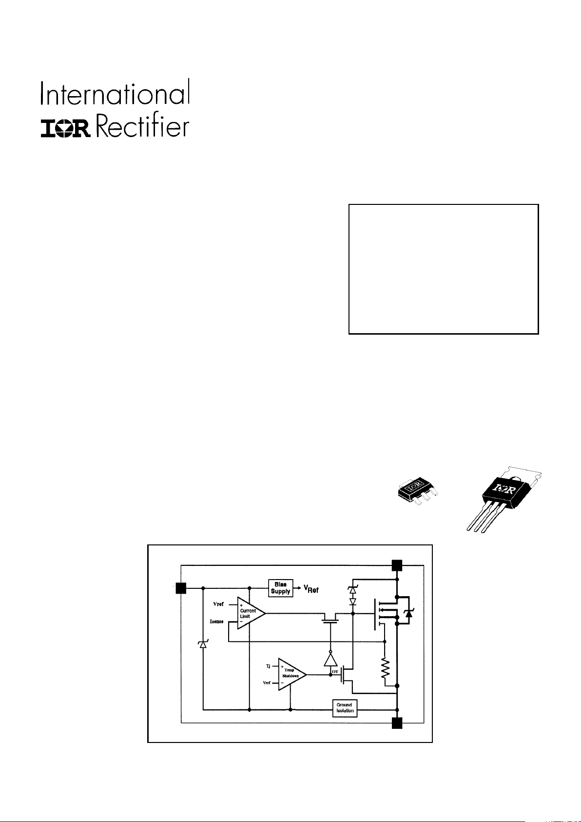
The IRSF3021 Lamp and DC Motor Driver is a fully protected three
terminal monolithic SMART POWER MOSFET that features current
limiting, over-temperature protection, gate-to-source ESD protection
and gate-to-drain clamp for over-voltage protection.
The on-chip protection circuit limits the drain current in the on-state.
The over-temperature circuitry turns off the POWER MOSFET when
the junction temperature exceeds 165°C. The device restarts automatically once it has cooled down below the reset temperature.
The IRSF3021 is specifically designed for driving loads that require
overload protection and in-rush current control while operating in automotive and industrial environments. Targeted applications include
resistive loads such as lamps or capacitive loads such as airbag squibs
and DC motor drives.
V
ds(clamp)
50 V
R
ds(on)
200 m
Ω
I
lim
3.0 A
T
j(sd)
165
o
C
E
AS
200 mJ
FULLY PROTECTED POWER MOSFET SWITCH
Features
■ Controlled Slew Rate Reduces EMI
■ Over Temperature Protection with Auto-Restart
■ Linear Current-Limit Protection
■ Active Drain-to-Source Clamp
■ ESD Protection
■ Compatible with Standard Power MOSFET
■ Low Operating Input Current
■ Monolithic Construction
■ Logic Level Input Threshold
Applications
■ Cabin Lighting
■ Airbag System
■ Programmable Logic Controller
■ DC Motor Drive
Available Packages
IRSF3021L
(SOT-223)
IRSF3021
(TO-220AB)
IRSF3021
IRSF3021 Block Diagram
Drain
Source
Input
Page 2
IRSF3021
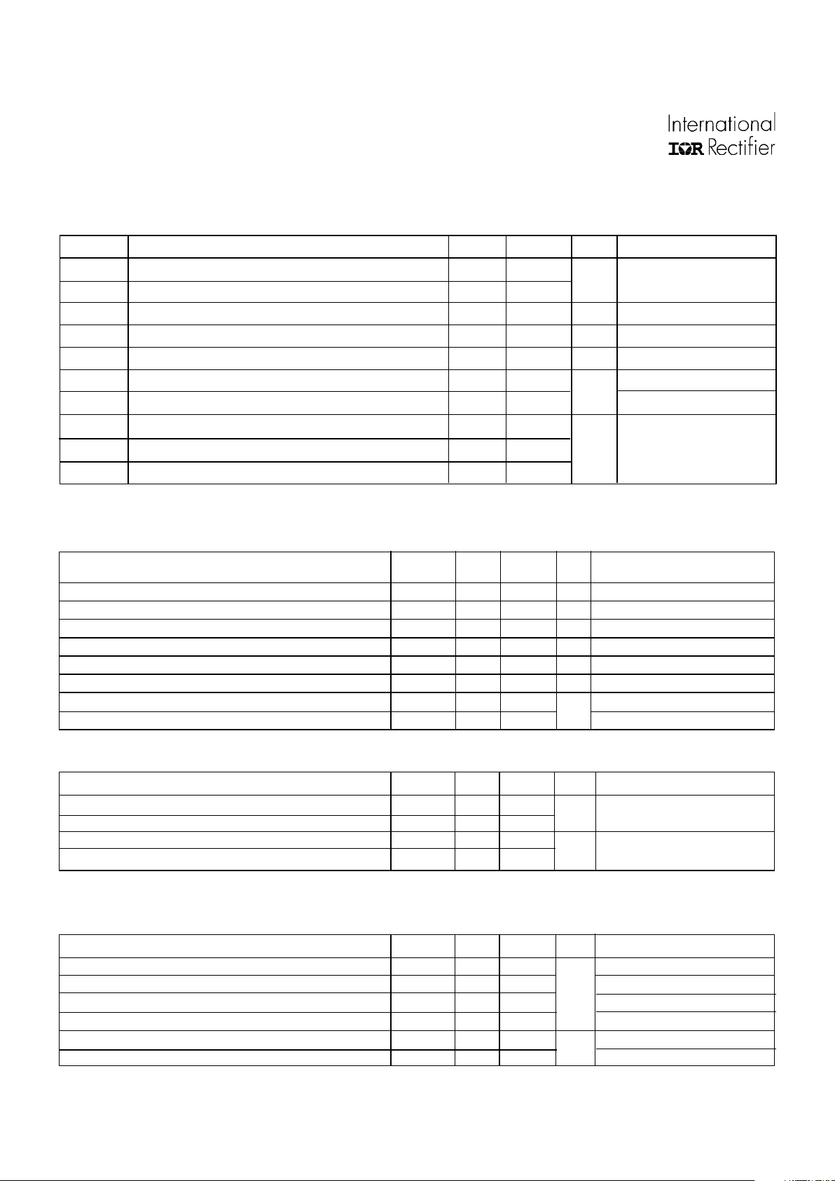
Absolute Maximum Ratings
Absolute Maximum Ratings indicate sustained limits beyond which damage to the device may occur. (Tc = 25°C unless
otherwise specified.)
Minimum Maximum Units Test Conditions
V
ds, max
Continuous Drain to Source Voltage 50
V
V
in, max
Continuous Input Voltage -0.3 8
I
ds
Continuous Drain Current self limited
P
d
Power Dissipation 30 W T
c
≤ 25°C
E
AS
Unclamped Single Pulse Inductive Energy 200 mJ
V
esd1
Electrostatic Discharge Voltage (Human Body Model) 4000
V
1000pF. 1.5kΩ
V
esd2
Electrostatic Discharge Voltage (Machine Model) 1000 200pF, 0Ω
T
Jop
Operating Junction Temperature Range -40
self-limited
T
Stg
Storage Temperature Range -40 175 °C
T
L
Lead Temperature (Soldering, 10 seconds) 300
Switching ElectricalCharacteristics
(VCC = 14V, Resistive Load (RL) = 10Ω, Rin= 100Ω. Specifications measured at TC= 25°C unless otherwise specified.)
Minimum Typical Maximum Units Test Conditions
t
don
Turn-On Delay Time 10 50 Vin = 0V to 5V, 50% to 90%
t
r
Rise Time 30 80
µs
Vin = 0V to 5V, 90% to 10%
t
doff
Turn-Off Delay Time 20 60 Vin = 0V to 5V, 50% to 10%
t
f
Fall Time 15 50 Vin = 0V to 5V, 10% to 90%
SR Output Positive Slew Rate -4 4
V/µs
Vin = 0V to 5V, +dVds/dt
SR Output Positive Slew Rate -4 4 Vin = 0V to 5V, -dVds/dt
Minimum Typical Maximum Units Test Conditions
V
ds,clamp
Drain to Source Clamp Voltage 50 56 65
V
Ids = 6A, tp = 700 µS
R
ds(on)
Drain to Source On Resistance 155 200 mΩ V
in
= 5V, Ids = 2A
I
dss
Drain to Source Leakage Current 250 µA Vds = 40V, Vin = 0V
V
th
Input Threshold Voltage 1.0 2.0 3.0 V V
ds
= Vin, Ids + Iin= 10mA
I
i,on
Input Supply Current (Normal Operation) 100 300 µ A Vin = 5V
I
i,off
Input Supply Current (Protection Mode) 500 µ A Vin = 5V
V
in, clamp
Input Clamp Voltage 9 10 V Iin = 1mA
V
sd
Body-Drain Diode Forward Drop➂ 1.5 V I
ds
= -2A, R
in
= 1kΩ
Static Electrical Characteristics
(Tc = 25°C unless otherwise specified.)
Minimum Typical Maximum Units Test Conditions
RΘ
jc
Junction to Case 4
°C/W TO-220AB
RΘ
jA
Junction to Ambient 60
RΘ
jc
Junction to PCB 40
°C/W SOT-223
RΘ
jA
Junction to PCB ➀ 60
Thermal Characteristics
Page 3

IRSF3021
Minimum Typical Maximum Units Test Conditions
I
ds(sd)
Current Limit 3.0 5.5 8.0 A Vin = 5V, VDS = 14V
T
j(sd)
Over Temperature Shutdown Threshold 155 165 °C Vin = 5V, Ids = 2A
V
protect
Min. Input Voltage for Over-temp function 3 V
t
Iresp
Current Limit Response Time TBD µs
I
peak
Peak Short Circuit Current 10 A
t
Tresp
Over-Temperature Response Time TBD µs
Protection Characteristics
(TC= 25 °C unless otherwise specified. Min/Max specifications are for TC= -40°C to TC = +125°C unless otherwise
specified.)
Notes:
① When mounted on a 1" square PCB (FR-4 or G10 material). For recommended footprint and soldering techniques, refer
to International Rectifier Application Note AN-994.
② E
AS
is tested with a constant current source of 6A applied for 700µS with Vin = 0V and starting Tj = 25°C.
③ Input current must be limited to less than 5mA with a 1kΩ resistor in series with the input when the Body-Drain Diode
is forward biased.
Page 4

IRSF3021
Case Outline SOT-223 (IRSF3021L)
MILLIMET ERS INCHES
DIM MIN MAX MIN MAX
A 1.55 1.80 0.061 0.071
B 0.65 0.85 0.026 0.033
B1 2.95 3.15 0.11 6 0.124
C 0.25 0.35 0.010 0.014
D 6.30 6.70 0.248 0.264
E 3.30 3.70 0.130 0.146
e 2.30 BSC .0905 BSC
e1 4.60 BSC 0.181 BSC
H 6.71 7.29 0.287 0.264
L — 0.91 — 0.036
L1 0.02 0.10 0.0006 0.004
Θ 10° MAX 10° MAX
NOTES:
1. Dimensioning and tolerancing per ANSI Y14.5M, 1982
2. Controlling dimension: INCH
3. Dimensions do not include lead flash
4. Conforms to JEDEC outline TO-261AA
LEAD ASSIGNMENTS
1. Gate
2. Drain
3. Source
4. Drain
Page 5

IRSF3021
Tape and Reel SOT-223 (IRSF3021L)
NOTES:
1. Controlling dimension: MILLIMETER
2. Conforms to outline EIA-481 and EIA-541
3. Each ∅ 330.00 (13.00) reel contains 2,500 devices.
NOTES:
1. Controlling dimension: MILLIMETER
2. Conforms to outline EIA-481-1
3. Dimension measured at hub
4. Includes flange distortion at outer edge
Page 6

IRSF3021
Case Outline TO-220AB (IRSF3021)
WORLD HEADQUARTERS: 233 Kansas St., El Segundo, California 90245, Tel: (310) 322 3331
EUROPEAN HEADQUARTERS: Hurst Green, Oxted, Surrey RH8 9BB, UK Tel: ++ 44 1883 732020
IR CANADA: 7321 Victoria Park Ave., Suite 201, Markham, Ontario L3R 2Z8, Tel: (905) 475 1897
IR GERMANY: Saalburgstrasse 157, 61350 Bad Homburg Tel: ++ 49 6172 96590
IR ITALY: Via Liguria 49, 10071 Borgaro, Torino Tel: ++ 39 11 451 0111
IR FAR EAST: K&H Bldg., 2F, 3-30-4 Nishi-Ikeburo 3-Chome, Toshima-Ki, Tokyo Japan 171 Tel: 81 3 3983 0086
IR SOUTHEAST ASIA: 315 Outram Road, #10-02 Tan Boon Liat Building, Singapore 0316 Tel: 65 221 8371
http://www.irf.com/ Data and specifications subject to change without notice. 12/96
LEAD ASSIGNMENTS
1. Gate
2. Drain
3. Source
4. Drain
NOTES:
1. Dimensioning and tolerancing per ANSI Y14.5M, 1982
2. Controlling dimension: INCH
3. Dimensions shown are in millimeters (inches)
4. Conforms to JEDEC outline TO-251AA
5. Dimension does not include solder dip. Solder dip max. +0.16 (.006)
 Loading...