

Page 1

VS440FX
Motherboard
Technical Product Specification
Order Number 281812-003
October 1996
The VS440FX motherboard may contain design defects or errors known as errata. Characterized errata that
may cause the VS440FX motherboard’s behavior to deviate from published specifications are documented in
the VS440FX Motherboard Specification Update.
Page 2

Revision History
Revision
-001
-002
-003
Revision History Date
Preliminary release of the VS440FX Technical Product Specification. 4/96
Second release of the VS440FX Technical Product Specification. 5/96
Updated to reflect Fab E 10/96
This product specification applies only to standard VS440FX motherboards with BIOS
identifier CS1.
Changes to this specification will be published in the VS440FX Motherboard Specification
Update before being incorporated into a revision of this document.
Information in this document is provided in connection with Intel products. No license, express or implied, by estoppel or
otherwise, to any intellectual property rights is granted by this document. Except as provided in Intel’s Terms and Conditions of
Sale for such products, Intel assumes no liability whatsoever, and Intel disclaims any express or implied warranty, relating to
sale and/or use of Intel products including liability or warranties relating to fitness for a particular purpose, merchantability, or
infringement of any patent, copyright or other intellectual property right. Intel products are not intended for use in medical, life
saving, or life sustaining applications.
Intel retains the right to make changes to specifications and product descriptions at any time, without notice.
The VS440FX motherboard may contain design defects or errors known as errata. Current characterized errata are available
on request.
Contact your local Intel sales office or your distributor to obtain the latest specifications before placing your product order.
†
Third-party brands and names are the property of their respective owners.
Copies of documents which have an ordering number and are referenced in this document, or other Intel literature, may be
obtained from:
Intel Corporation
P.O. Box 7641
Mt. Prospect, IL 60056-7641
or call in North America 1-800-879-4683, Europe 44-0-1793-431-155, France 44-0-1793-421-777,
Germany 44-0-1793-421-333, other Countries 708-296-9333.
Copyright 1996, Intel Corporation
Page 3

Table of Contents
1 Motherboard Description
1.1 Overview......................................................................................................................7
1.2 Motherboard Manufacturing Options ...........................................................................9
1.3 Form Factor.................................................................................................................9
1.4 I/O Shield...................................................................................................................10
1.5 Microprocessor ..........................................................................................................11
1.5.1 Microprocessor Heatsink and Clips .............................................................11
1.5.2 Microprocessor Upgrade .............................................................................11
1.6 Main Memory.............................................................................................................12
1.6.1 EDO DRAM.................................................................................................12
1.6.2 Parity/ECC DRAM.......................................................................................12
1.7 Chipset ......................................................................................................................13
1.7.1 82441FX PCI Bridge and Memory Controller (PMC)...................................13
1.7.2 82442FX Data Bus Accelerator (DBX) ........................................................13
1.7.3 82371SB PCI/ISA IDE Xcelerator (PIIX3)....................................................13
1.7.4 Universal Serial Bus Support.......................................................................14
1.7.5 IDE Support.................................................................................................14
1.8 Super I/O Controller...................................................................................................15
1.8.1 Serial Ports..................................................................................................15
1.8.2 Parallel Port.................................................................................................15
1.8.3 Floppy Controller.........................................................................................15
1.8.4 Keyboard and Mouse Interface...................................................................16
1.8.5 Real-Time Clock, CMOS RAM, and Battery ................................................16
1.8.6 Infrared Support ..........................................................................................17
1.9 Audio Subsystem.......................................................................................................17
1.9.1 Audio Drivers and Utilities............................................................................18
1.9.2 CD-ROM Audio Connector..........................................................................18
1.9.3 Telephony Connector..................................................................................18
1.9.4 Wavetable Connector..................................................................................18
1.10 Management Extension Hardware.............................................................................19
1.11 Motherboard Connectors...........................................................................................20
1.11.1 CD Audio (J1E2)..........................................................................................21
1.11.2 Wavetable Upgrade Connector (J1E1)........................................................21
1.11.3 Telephony Connector (J1F1).......................................................................21
1.11.4 Floppy Drive Connector (J9J2)....................................................................22
1.11.5 PCI IDE Connectors (J9J1, J8J1)................................................................23
1.11.6 Power Supply Connector (J5M1).................................................................23
1.11.7 Microprocessor Fan Connector (J7M1) .......................................................24
1.11.8 Auxiliary Fan Connector (J9A1)...................................................................24
1.11.9 Front Panel Connectors...............................................................................25
1.11.10 Back Panel Connectors...............................................................................27
1.12 Add-in Board Expansion Connectors.........................................................................31
iii
Page 4

VS440FX Motherboard Technical Product Specification
1.13 Jumper Settings.........................................................................................................33
1.13.1 Processor Configuration (J6D1)..................................................................34
1.13.2 Password Clear (J6D1)................................................................................34
1.13.3 Clear CMOS (J6D1).....................................................................................35
1.13.4 BIOS Setup Access (J6D1).........................................................................35
1.13.5 BIOS Recovery (J6D1)................................................................................35
1.14 Reliability ...................................................................................................................35
1.15 Environmental............................................................................................................35
1.16 Power Supply Requirements .....................................................................................36
1.17 Power Consumption ..................................................................................................36
1.18 Regulatory Compliance..............................................................................................37
1.18.1 Safety..........................................................................................................37
1.18.2 Electromagnetic Interference (EMI).............................................................38
1.18.3 Product Certification Markings.....................................................................38
2 Motherboard Resources
2.1 Memory Map..............................................................................................................39
2.2 DMA Channels...........................................................................................................39
2.3 I/O Map......................................................................................................................40
2.4 PCI Configuration Space Map ...................................................................................42
2.5 Interrupts ...................................................................................................................42
3 BIOS and Setup Utility
3.1 Introduction................................................................................................................43
3.2 BIOS Flash Memory Organization .............................................................................43
3.3 BIOS Upgrades..........................................................................................................44
3.4 PCI IDE Support........................................................................................................44
3.5 PCI Auto-configuration...............................................................................................45
3.6 ISA Plug and Play......................................................................................................45
3.7 Desktop Management Interface.................................................................................45
3.8 Advanced Power Management..................................................................................46
3.9 Advanced Power Control...........................................................................................47
3.10 Language Support.....................................................................................................47
3.11 Boot Options..............................................................................................................47
3.12 Flash LOGO Area......................................................................................................47
3.13 BIOS Setup Access Jumper ......................................................................................48
3.14 Recovering BIOS Data ..............................................................................................48
3.15 BIOS Setup Utility......................................................................................................48
3.15.1 Overview of the Setup Menu Screens.........................................................48
3.15.2 Main BIOS Setup Screen............................................................................49
3.15.3 Floppy Options Subscreen..........................................................................50
3.15.4 Primary/Secondary IDE Master/Slave Configuration Subscreens..............51
3.15.5 Boot Options Subscreen .............................................................................53
3.15.6 Advanced Screen........................................................................................56
3.15.7 Peripheral Configuration Subscreen............................................................57
3.15.8 Advanced Chipset Configuration Subscreen...............................................59
3.15.9 Power Management Configuration Subscreen............................................60
3.15.10 Plug and Play Configuration Subscreen......................................................61
iv
Page 5

3.15.11 Event Logging Configuration Subscreen.....................................................62
3.15.12 Security Screen...........................................................................................63
3.15.13 Security Screen Options..............................................................................64
3.15.14 Exit Screen..................................................................................................65
4 Error Messages and Beep Codes
4.1 BIOS Beep Codes.....................................................................................................6 7
4.2 PCI Configuration Error Messages ............................................................................68
4.3 BIOS Error Messages................................................................................................6 9
4.4 ISA NMI Messages....................................................................................................70
5 Compliance with Specifications
5.1 Specifications.............................................................................................................71
5.2 Online Support...........................................................................................................71
Tables
1. PCI Bus Connectors..................................................................................................31
2. ISA Bus Connectors ..................................................................................................32
3. Jumper Settings.........................................................................................................34
4. Jumper Settings for Processor and Host Bus Frequencies........................................34
5. Motherboard Environmental Specifications................................................................35
6. DC Voltage ................................................................................................................36
7. Power Usage.............................................................................................................37
8. Memory Map..............................................................................................................39
9. DMA Channels...........................................................................................................39
10. I/O Map......................................................................................................................40
11. PCI Configuration Space Map ...................................................................................42
12. Interrupts ...................................................................................................................42
13. Flash Memory Organization.......................................................................................43
14. Recommendations for Configuring an ATAPI Device ................................................44
15. Overview of the Setup Menu Screens .......................................................................48
16. Administrative and User Password Functions............................................................64
Contents
Figures
1. Motherboard Components...........................................................................................8
2. Motherboard Dimensions.............................................................................................9
3. Back Panel I/O Shield (with Audio option) Dimensions..............................................10
4. Motherboard Connectors...........................................................................................20
5. Front Panel I/O Connectors.......................................................................................25
6. Back Panel I/O Connectors .......................................................................................28
7. Jumper Locations ......................................................................................................33
v
Page 6

Page 7

1 Motherboard Description
1.1 Overview
The VS440FX motherboard supports Pentium® Pro microprocessors operating at 150, 166, 180,
and 200 MHz. The Pentium Pro microprocessor includes 16 KB of L1 cache on the chip. A
256 KB or 512 KB L2 cache device is contained in the same package as the microprocessor. The
motherboard features:
• ATX form factor
• Socket 8 Pentium Pro processor socket
Main Memory
†
• Four 72-pin SIMM
• Support for up to 256 MB of Extended Data Out (EDO) or fast page memory
• Support for non-parity, parity, or Error Checking and Correcting (ECC) DRAM
Chipset and PCI/IDE Interface
• Intel 82440FX PCIset
• Integrated PCI bus mastering controller
• Two fast IDE interfaces
• Support for up to four IDE drives or devices
• Support for two Universal Serial Bus (USB) interfaces
sockets
I/O Features
• PC87308/87307 Super I/O controller
• Integrates standard I/O functions: floppy drive interface, one multi-mode parallel port, two
FIFO serial ports, real-time clock, keyboard and mouse controller, and IrDA
interface
Expansion Slots
• Three ISA
• Three PCI
• One shared PCI/ISA
Audio Subsystem
• Crystal
• Wavetable upgrade header
Other features
• Plug and Play compatible BIOS
• Support for Advanced Power Management (APM)
†
CS4236 Multimedia codec
†
-compatible
7
Page 8
VS440FX Motherboard Technical Product Specification
OM05506
J
L
K
M
Y
X
AA
DCBA
CC
BB
E
OS R PQW TV U
N
F H IG
Z
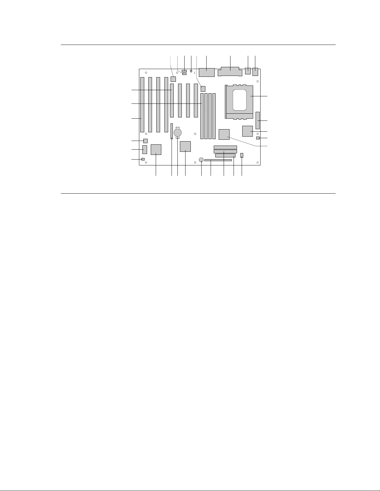
Figure 1. Motherboard Components
A. Optional Crystal Audio device P. Floppy connector
B. Optional CD-ROM audio connector Q. IDE connectors
C. Optional wavetable connector R. Front panel connectors
D. Optional telephony connector S. Onboard speaker
E. VCCP voltage regulator T. Intel 82371SB PIIX3
F. MIDI/game port/audio jacks U. Battery
G. Parallel port/serial connectors V. Jumper block
H. Optional USB connectors W. National PC87308/87307 Super I/O controller
I. Keyboard and mouse connectors X. Auxiliary fan connector
J. Pentium Pro microprocessor / Socket 8 Y. Flash BIOS
K. Power connector Z. Management Extension Hardware ASIC
L. Intel 82441FX AA. ISA add-in board connectors
M. Microprocessor fan connector BB. SIMM connectors
N. Intel 82442FX CC. PCI add-in board connectors
O. VTT voltage regulator
8
Page 9
Motherboard Description
OM05522
9.20
3.10
0.65
9.60
8.25
0.25
0.0
0.0 12.00
3.75 5.55
11.75
1.2 Motherboard Manufacturing Options
• Support for USB
• Audio Option
CS4236 audio codec
CD-ROM connector
Wavetable upgrade connector
Telephony connector
MIDI/game port/audio jacks
• Management Extension Hardware ASIC
1.3 Form Factor
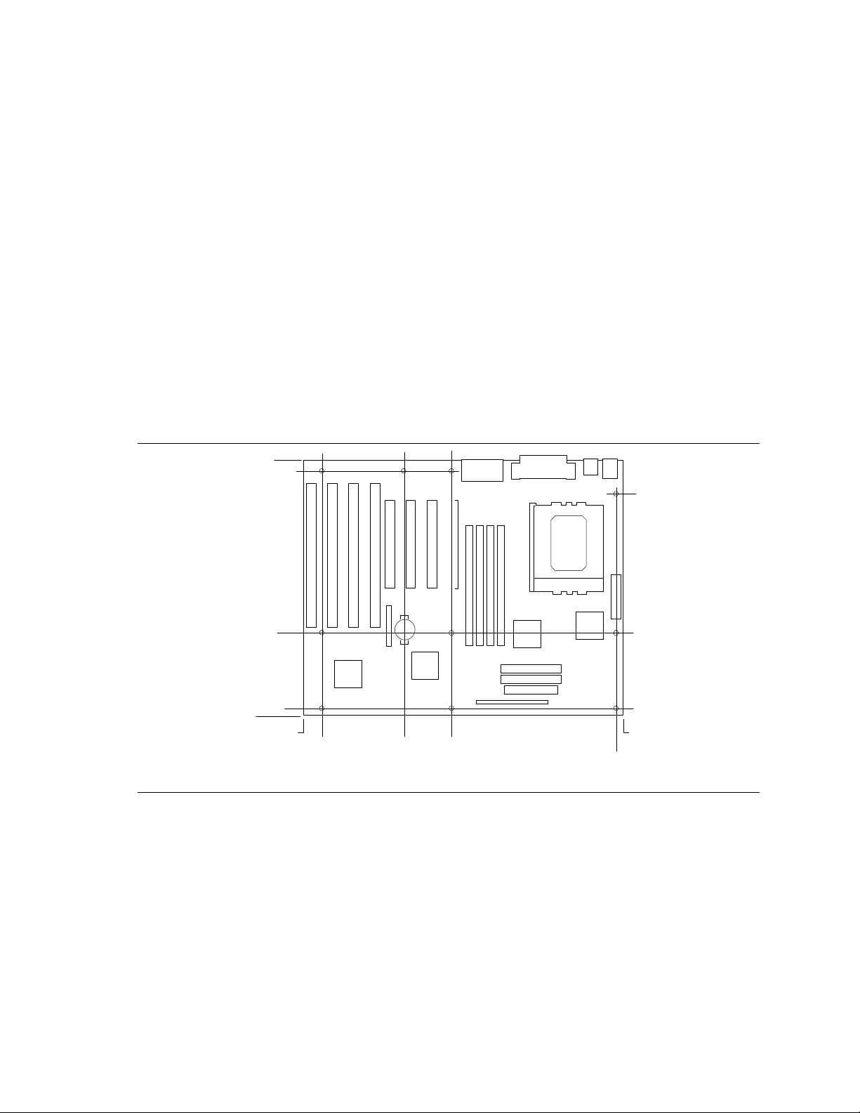
The motherboard is designed to fit into a standard ATX form factor chassis. Figure 2 illustrates the
mechanical form factor for the motherboard. Location of the I/O connectors and mounting holes is
in strict compliance with the ATX specification (refer to Section 5.1).
Figure 2. Motherboard Dimensions
9
Page 10
VS440FX Motherboard Technical Product Specification
Left-end View
OM05588
Note: Material = 0.010 ±.0.001 Thick Stainless Steel, Half Hard
0.671
1.955
0.597
0.553
1.911
2.184
3.327
4.735
4.899
5.391
5.883
6.533
0.193
0.768
0.295
0.458
1.158
0.666
4.610
1.590
0.200
1.407
0.652
0.133
0.120
2.055
2.326
2.023
0.050
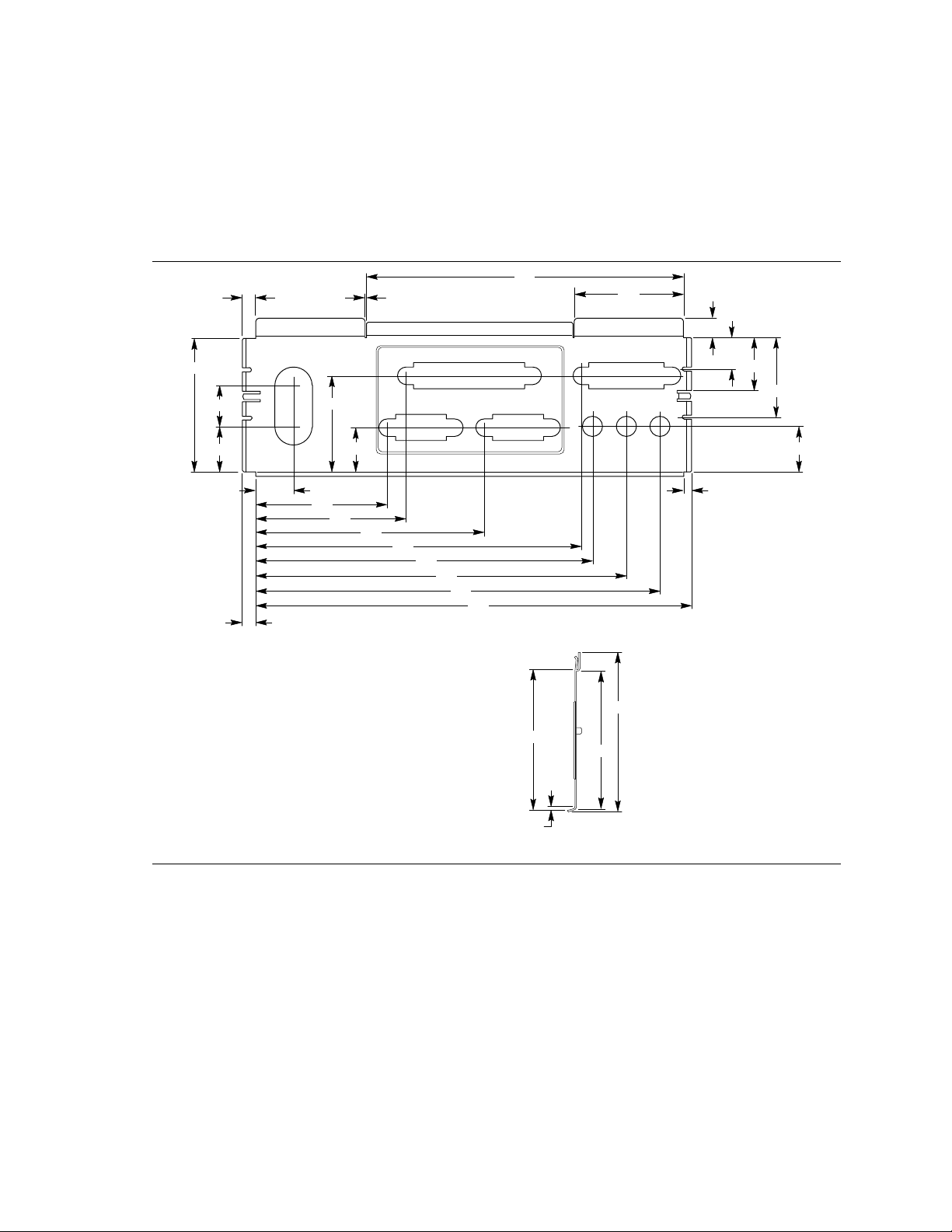
1.4 I/O Shield
The back panel I/O shield for the VS440FX motherboard must meet specific dimensional and
material requirements. Computers based on this motherboard need the back panel I/O shield in
order to pass certification testing. Figure 3 shows the critical dimensions for both options of the
I/O shield and indicates the position of each cutout.
Figure 3. Back Panel I/O Shield (with Audio option) Dimensions
10
Page 11

Motherboard Description
1.5 Microprocessor
The motherboard operates with 2.1 V to 3.5 V Pentium Pro processors. The onboard voltage
regulator is automatically programmed and controlled by the VID pins of the processor to provide
the required voltage. The motherboard supports Pentium Pro processors that run internally from
150 MHz up to 200 MHz.
The motherboard supports Pentium Pro processors with either 256 KB or 512 KB of second-level
cache.
The processor maintains full backward compatibility with the 8086, 80286, Intel386
and Pentium processors. Its numeric coprocessor maintains backward compatibility with math
coprocessors and that comply with ANSI/IEEE standard 754-1985.
1.5.1 Microprocessor Heatsink and Clips
CAUTION
Do not use the older style of bail-wire clips for securing the heat sink assembly. These clips have
been known to damage the motherboard when installed or removed incorrectly.
TM
, Intel486TM,
An approved Pentium Pro processor heat sink is necessary for proper thermal dissipation. The
processor/heat sink assembly must be securely fastened to the ZIF socket by two clips. These clips
fit over the heat sink assembly and attach to tabs on the socket.
1.5.2 Microprocessor Upgrade
The motherboard has a Socket 8 processor socket. Socket 8 is a 387-pin modified staggered pin
grid array (SPGA) ZIF socket with a voltage regulator for the processor core. The socket supports
upgrades to future Pentium Pro OverDrive
®
processors.
11
Page 12

VS440FX Motherboard Technical Product Specification
1.6 Main Memory
The motherboard has four SIMM sockets arranged in two banks: Bank 0 and Bank 1. Each bank
has two sockets. SIMMs in the same bank must be the same type, size, and speed; SIMMs in
different banks may differ in type, size, and speed. SIMMs must be installed in both sockets of a
bank, and at least one bank must be filled. The BIOS automatically detects memory type and size
so no jumper settings are required.
The motherboard supports:
• 72-pin SIMMs with tin-plated contacts
• 60 ns fast page mode SIMMs or 60 ns EDO SIMMs
• Non-parity, parity, or ECC SIMMs
• Single- or double-sided SIMMs in the following sizes:
Configuration
SIMM size
4 MB 1 x 32 1 x 36
8 MB 2 x 32 2 x 36
16 MB 4 x 32 4 x 36
32 MB 8 x 32 8 x 36
64 MB 16 x 32 16 x 36
(non-parity)
Configuration
(parity)
1.6.1 EDO DRAM
EDO DRAM improves memory read performance by holding the memory data valid until the next
CAS# falling edge, unlike fast page mode DRAM, which tri-states the memory data when CAS#
negates to precharge for the next memory cycle. With EDO DRAM, the CAS# precharge overlaps
the data-valid time, which allows CAS# to negate earlier while still satisfying the memory-data
valid window.
1.6.2 Parity/ECC DRAM
Memory error checking and correction is supported by parity memory. With parity memory, the
motherboard can be configured to support ECC memory operation. Parity SIMMs are
automatically detected, but you must enter Setup to configure the memory for either Parity or ECC
operation. Parity memory detects single-bit errors. ECC memory detects double-bit errors and
corrects single-bit errors.
12
Page 13

Motherboard Description
1.7 Chipset
The Intel 82440FX PCIset consists of the 82441FX PCI Bridge and Memory Controller (PMC),
the 82442FX Data Bus Accelerator (DBX), and one 82371SB PCI/ISA IDE Xcelerator (PIIX3)
bridge chip.
1.7.1 82441FX PCI Bridge and Memory Controller (PMC)
The PMC provides all control signals necessary to drive second level cache and main memory,
including multiplexed address signals. It also controls system access to memory and generates
snoop controls to maintain cache coherency. The PMC comes in a 208-pin QFP package that
features:
• Microprocessor interface control
• Integrated L2 write-back cache controller
256 or 512 KB direct-mapped
• Integrated DRAM controller
64/72-bit non-interleaved path to memory
EDO and fast page DRAM support
Non-parity, parity, and ECC support
• Fully synchronous PCI bus interface
30 and 33 MHz bus speeds
PCI to DRAM data throughput at greater than 100 MB per second
Up to four PCI masters in addition to the PIIX3 and IDE
• Data Buffering
Pentium Pro processor-to-DRAM and PCI-to-DRAM write data buffering
Pentium Pro-processor-to-PCI burst writes
1.7.2 82442FX Data Bus Accelerator (DBX)
The DBX connects to the 64-bit Pentium Pro data bus, the 64/72-bit memory data bus, and the
16 bit PMC private data bus. The DBX works in parallel with the PMC to provide a high
performance memory subsystem for Pentium Pro processor based systems. The DBX comes in a
208-pin QFP package.
1.7.3 82371SB PCI/ISA IDE Xcelerator (PIIX3)
The PIIX3 is the interface between the PCI and ISA buses. It features an integrated dual-channel
enhanced IDE interface that supports up to four IDE devices. The PIIX3 comes in a 208-pin QFP
package that features:
• PCI and ISA bus interface
• USB host/hub controller
13
Page 14

VS440FX Motherboard Technical Product Specification
• Integrated dual-channel enhanced IDE interface
Support for up to four IDE devices
PIO Mode 4 transfers at up to 16 MB per second
Integrated 8 x 32-bit buffer for bus master PCI IDE burst transfers
Bus master mode
• PCI compliance (refer to Section 5.1)
• Enhanced DMA controller supporting up to seven DMA channels
• Interrupt controller with PCI-to-ISA interrupt mapping circuitry
• A 16-bit counter/timer
• SMI interrupt logic and timer with fast on/off mode
• NMI circuitry
1.7.4 Universal Serial Bus Support
The motherboard features two optional USB ports. The ports permit the direct connection of two
USB peripherals without an external hub. If more devices are required, an external hub can be
connected to either of the built-in ports. The motherboard fully supports the standard universal
host controller interface (UHCI) and uses standard software drivers that are UHCI-compatible.
Features of the USB include:
• Self-identifying, hot pluggable peripherals.
• Automatic mapping of function to driver and configuration.
• Support for isochronous and asynchronous transfer types over the same set of wires.
• Support for up to 127 physical devices.
• Support for full speed (12 Mbs) and low speed (1.5 Mbs) USB connections. Full speed
connections require shielded cabling.
• Guaranteed bandwidth and low latencies appropriate for telephony, audio, and other
applications.
• Error handling and fault recovery mechanisms built into protocol.
1.7.5 IDE Support
The motherboard has two independent bus mastering PCI IDE interfaces that support PIO Mode 3,
PIO Mode 4, and ATAPI (e.g., CD-ROM) devices. The BIOS supports Logical Block Addressing
(LBA) and Extended Cylinder Head Sector (ECHS) translation modes. IDE device transfer rate
and translation mode are automatically detected by the BIOS.
Normally, programmed I/O operations require a substantial amount of processor bandwidth;
however, in true multi-tasking operating systems such as Windows
mastering IDE can be devoted to other tasks while disk transfers are occurring.
14
†
95, the bandwidth freed by bus
Page 15

Motherboard Description
1.8 Super I/O Controller
The PC87308/87307 Super I/O Controller from National Semiconductor is a fully Plug and Play
compatible device which provides:
• Serial ports: two NS16C550-compatible UARTs with send/receive 16-byte FIFO
• Multimode bidirectional parallel port
†
Standard mode, IBM
Enhanced Parallel Port (EPP) mode with BIOS and driver support
High-speed Extended Capabilities Port (ECP) mode
• Industry standard floppy controller with 16-byte FIFO and 2.88 MB floppy drive support
• 8042-compatible keyboard controller
• Real-time clock accurate within ±13 minutes a year at 25 ºC and 5 V
• Support for an IrDA-compliant infrared interface
By default, the I/O controller interfaces are automatically configured during boot up. The I/O
controller can also be manually configured in the Setup program.
1.8.1 Serial Ports
and Centronics† compatible
The motherboard has two 9-pin D-Sub serial port connectors located on the back panel. The
NS16C550-compatible UARTs support data transfers at speeds up to 921.6 kBaud (standard) or
1.5 MBaud.
1.8.2 Parallel Port
The connector for the multimode bidirectional parallel port is a 25-pin D-Sub connector located on
the back panel of the motherboard. In the Setup program, there are four options for parallel port
operation:
• Compatible (standard mode).
†
• Bidirectional (PS/2
• Bidirectional EPP. A driver from the peripheral manufacturer is required for operation.
• Bidirectional high-speed ECP.
compatible).
1.8.3 Floppy Controller
The I/O controller is software compatible with the DP8473 and 82077 floppy drive controllers. In
the Setup program, the floppy interface can be configured for the following floppy drive capacities
and sizes:
• 360 KB, 5.25-inch
• 1.2 MB, 5.25-inch
• 720 KB, 3.5-inch
• 1.2 MB, 3.5-inch (driver required)
• 1.25/1.44 MB, 3.5-inch
• 2.88 MB, 3.5-inch
15
Page 16

VS440FX Motherboard Technical Product Specification
1.8.4 Keyboard and Mouse Interface
PS/2 keyboard and mouse connectors are located on the back panel of the motherboard. The 5 volt
lines to these connectors are protected with a PolySwitch
reestablishes the connection after an over-current condition is removed. While this device
eliminates the possibility of having to replace a fuse, power to the computer should be turned off
before connecting or disconnecting a keyboard or mouse.
NOTE
✏
You can plug the mouse and keyboard into either connector.
The keyboard controller contains the AMI Megakey keyboard and mouse controller code, which
provides the traditional keyboard and mouse control functions, and also supports Power On/Reset
password protection. A Power On/Reset password can be specified in the Setup program.
The keyboard controller also supports the following hot-key sequences:
• <CTRL><ALT><DEL> Software reset. This key sequence resets the computer’s software by
jumping to the beginning of the BIOS code and running the Power On Self Test (POST).
• <CTRL><ALT><+> and <CTRL><ALT><-> Turbo mode. Note that Turbo mode could be
affected by the operating system, or whether the processor is in protected mode or virtual
x86 mode.
<CTRL><ALT><-> For Deturbo mode (emulates a 23 MHz AT)
<CTRL><ALT><+> For Turbo mode
• <CTRL><ALT><defined in Setup> Power management. This key sequence invokes power
managed mode, which reduces the computer’s power consumption while maintaining its ability
to service external interrupts.
• <CTRL><ALT><defined in Setup> Keyboard lock. This key sequence is a security feature
that locks the keyboard until the User password is entered. When keyboard lock is invoked,
the keyboard LEDs flash. To enable the keyboard lock feature, a User password must be
specified in the Setup program.
†
circuit that, like a self-healing fuse,
1.8.5 Real-Time Clock, CMOS RAM, and Battery
The real-time clock is compatible with DS1287 and MC146818 components. It provides a timeof-day clock and a 100-year calendar with alarm features and century rollover. The real-time clock
also supports 242-bytes of battery-backed CMOS RAM in two banks, which are reserved for
BIOS use.
The time, date, and CMOS values can be specified in the Setup program. The CMOS values can
be returned to their defaults by using the Setup program or by setting a configuration jumper on the
motherboard.
An external coin-cell battery powers the real-time clock and CMOS memory. If the computer is
not plugged into a wall socket, the battery has an estimated life of three years. When the computer
is plugged in, the 5 volt standby current from the motherboard’s power supply extends the life of
the battery. The RTC is accurate to ±13 minutes/year at 25 ºC and 5 V conditions.
16
Page 17

Motherboard Description
1.8.6 Infrared Support
The motherboard has a 5-pin header that supports Hewlett Packard† HSDSL-1000 compatible
infrared (IR) transmitters/receivers. The connection can be used to transfer files to or from portable
devices like laptops, PDAs, and printers. The Infrared Data Association (IrDA) specification
supports data transfers of 115 Kbps at a distance of 1 meter.
1.8.6.1 Consumer Infrared Support
The motherboard has a signal pin that supports Consumer IR devices (remote controls). The signal
pin supports receive only. Consumer IR devices can be used to control telephony functions and
multimedia operations like volume and CD track changes. A software and hardware interface is
needed to use this feature.
1.9 Audio Subsystem
The optional onboard audio subsystem features the Crystal CS4236, a 100-pin TQFP audio codec
with an integrated FM synthesizer. The audio subsystem provides all the digital audio and analog
mixing functions needed for recording and playing sound on personal computers. Together, these
components feature:
• Stereo analog-to-digital and digital-to-analog converters
• Analog mixing, anti-aliasing, and reconstruction filters
• Line and microphone level inputs
• ADPCM, A-law, or µlaw digital audio compression/decompression
• Full digital control of all mixer and volume control functions
• Full duplex operation
• Sound Blaster† game and Windows Sound System compatibility
17
Page 18

VS440FX Motherboard Technical Product Specification
I/O Address
(Options)
210-21Fh
220-22Fh (best choice)
230-234h
240-24Fh
250-25Fh
260-26Fh
534-537h (best choice)
608-60Bh
300-301h
330-331h (best choice)
332-333h
334-335h
200-207h
388-308Bh
FF0-FFFh
The audio subsystem requires up to two DMA channels and two IRQs. The following table shows
the IRQ, DMA channel, and base I/O address options.
Resource
Sound Blaster
(DMA playback, DMA / IRQ shared
with Windows Sound System capture)
Windows Sound System
(DMA playback)
MPU-401
(IRQ shared with Sound Blaster)
MIDI / Game Port
FM Synthesis
CS4236 Control
IRQ
(Options)
5 (best choice)
7
9
11
5
7
9 (best choice)
11
5 (best choice)
7
9
11
DMA channel
(Options)
0 (best choice)
3
0
1 (best choice)
3
1.9.1 Audio Drivers and Utilities
Audio software and utilities are available from Intel’s World Wide Web site (refer to Section 5.2).
1.9.2 CD-ROM Audio Connector
A 1 x 4-pin connector is available for connecting an internal CD-ROM reader to the audio
subsystem’s mixer. The connector is compatible with most cables supplied with ATAPI CD-ROM
readers designed to connect to audio add-in cards.
1.9.3 Telephony Connector
A 2 x 2-pin connector is available for connecting the monaural audio signals of an internal
telephony device such as a fax/modem to the motherboard’s audio subsection. The mono-in and
mono-out signal interface is necessary for telephony applications such as speakerphones and
answering machines.
1.9.4 Wavetable Connector
An 8-pin connector supports wavetable add-in cards. Most wavetable add-in cards are installed in
a standard ISA slot; a cable is then routed from the card to the connector.
Compatible wavetable cards are available from several vendors. The ICS WaveFront and the
CrystaLake Series 2000 wavetable product families offer general MIDI-compatible audio
operation.
18
Page 19

Motherboard Description
1.10 Management Extension Hardware
The optional Management Extension hardware provides low-cost instrumentation capabilities
designed to reduce the total cost of owning a PC. The hardware implementation is a single-chip
ASIC. Features include:
• An integrated temperature sensor
• Fan speed sensors for up to three fans
• Power supply voltage monitoring to detect levels above or below acceptable values
• Registers for storing POST hardware test results and error codes
• Security switch for detecting physical intrusion, such as when the chassis lid has been removed
(even when power is off). A photosensor is used as the switch.
• Remote reset capabilities from a remote peer or server through LANDesk
Version 3.0 and service layers (when available)
• Hardware compatibility with Windows NT
†
When suggested ratings for temperature, fan speed, or voltage are exceeded, an interrupt is
activated.
The Management Extension circuitry connects to the ISA bus as an 8-bit I/O mapped device. It
uses these I/O addresses:
Client Manager,
Address (hex)* Description
80 POST codes
85 Address and control functions of the ASIC
86 Register read/write operations for the ASIC
* These addresses are accessible only when the processor is in System
Management Mode.
19
Page 20
VS440FX Motherboard Technical Product Specification
Secondary
Primary
OM05523
Simm
Socket(4)
1(J3G1, J3G2)
0
(J3H1, J3H2)
J2D1, J2D2
J2E1, J2F1
PCI
Connectors(4)
J1A1, J1B1
J1B2, J1C1
ISA
Connectors(4)
1
3
J9A1
Aux Fan
Connector
14
J1E2
CDROM
Connector
1
J1E1
Wave Table
Connector
2
J1F1
Telephony
Connector
1
13
J7M1
CPU Fan
Connector
1
10
11
20
J5M1
Power
Connector
J9J2
2
34
1
335
Floppy Drive Connector
PCI IDE Connector(2)
139
24020
J8J1
J9J1
Front Panel I/O Connector
J10H1
27 1
1.11 Motherboard Connectors
The following figure shows the connectors on the motherboard.
Figure 4. Motherboard Connectors
20
Page 21

1.11.1 CD Audio (J1E2)
Pin Signal Name
1 Ground
2 CD audio left channel
3 Ground
4 CD audio right channel
1.11.2 Wavetable Upgrade Connector (J1E1)
Pin Signal Name
1 Wave in right
2 Ground
3 Wave in left
4 Ground
5 No connection
6 Ground
7 No connect
8 MIDI_Out
Motherboard Description
1.11.3 Telephony Connector (J1F1)
Pin Signal Name
1 Ground
2 Audio out
3 Audio in
4 Key
21
Page 22

VS440FX Motherboard Technical Product Specification
Pin
2
4
6
8
10
12
14
16
18
20
22
24
26
28
30
32
34
1.11.4 Floppy Drive Connector (J9J2)
Pin Signal Name
1 Ground
3 Ground
5 Key
7 Ground
9 Ground
11 Ground
13 Ground
15 Ground
17 MSEN1
19 Ground
21 Ground
23 Ground
25 Ground
27 MSEN0
29 Ground
31 Ground
33 Ground
Signal Name
DENSEL
Reserved
FDEDIN#
FDINDX# (Index)
FDM00# (Motor enable A)
FDDS1# (Drive select B)
FDDS0# (Drive select A)
FDM01# (Motor enable B)
FDDIR#
FDSTEP#
FDWD# (Write data)
FDWE# (Write gate)
FDTRK0# (Track 0)
FDWPD# (Write protect)
FDRDATA# (Read data)
FDHEAD# (Side 1 select)
DSKCHG# (Diskette change)
22
Page 23

1.11.5 PCI IDE Connectors (J9J1, J8J1)
Pin
2
4
6
8
10
12
14
16
18
20
22
24
26
28
30
32
34
36
38
40
Motherboard Description
Pin Signal Name
1 Reset IDE
3 Host data 7
5 Host data 6
7 Host data 5
9 Host data 4
11 Host data 3
13 Host data 2
15 Host data 1
17 Host data 0
19 Ground
21 DDRQ0 [DDRQ1]
23 I/O write#
25 I/O read#
27 IOCHRDY
29 DDACK0# [DDACK1#]
31 IRQ 14 [IRQ 15]
33 Address 1
35 Address 0
37 Chip select 1P# [Chip select 1S#]
39 Activity#
NOTE: Signal names in brackets are for the secondary IDE connector
Signal Name
Ground
Host data 8
Host data 9
Host data 10
Host data 11
Host data 12
Host data 13
Host data 14
Host data 15
Key
Ground
Ground
Ground
Vcc pull-up
Ground
Reserved
Reserved
Address 2
Chip select 3P# [Chip select 3S#]
Ground
1.11.6 Power Supply Connector (J5M1)
An ATX power supply supports remote power on/off through pin 14 of the power supply
connector. This enables the motherboard to turn off system power through software control.
To enable soft-off control in software, APM must be enabled in the Setup program and in the
operating system. When the system BIOS receives the correct APM command from the operating
system, the BIOS turns off power to the computer. For example, in the Windows 95 Start menu,
the user selects Shutdown to turn off the power.
23
Page 24

VS440FX Motherboard Technical Product Specification
With soft-off enabled, if power to the computer is interrupted by a power outage or a disconnected
power cord, when power resumes the computer returns to the on or off state it was in before power
was interrupted.
Pin Signal Name
1 +3.3 V
2 +3.3 V
3 Ground
4 +5 V
5 Ground
6 +5 V
7 Ground
8 PWRGD (Power Good)
9 +5 VSB (Standby)
10 +12 V
11 +3.3 V
12 -12 V
13 Ground
14 PS-ON# (Power Supply Remote
On/Off Control)
15 Ground
16 Ground
17 Ground
18 -5 V
19 +5 V
20 +5 V
1.11.7 Microprocessor Fan Connector (J7M1)
Pin Signal Name
1 Ground
2 +12V
3 Sense tachometer
1.11.8 Auxiliary Fan Connector (J9A1)
Pin Signal Name
1 Ground
2 +12V
3 Sense tachometer
24
Page 25

1.11.9 Front Panel Connectors
OM04550
J10H1
27 1
SPKR HD LED SLPRST PWR LED INFRARED
PWR ON
613182224
The front panel connector includes headers for these I/O connections:
• Speaker
• Reset switch
• Power LED
• Hard drive activity LED
• Infrared (IrDA) port
• Sleep switch
• Power switch
Motherboard Description
Figure 5. Front Panel I/O Connectors
1.11.9.1 Front Panel I/O Connectors
Pin Signal Name Connector
1 SW_ON# Power On
2 Ground
3 SLEEP Sleep/Resume
4 SLEEP_PU (pullup)
5 No connect none
6 +5 V IrDA
7 Key
8 IrRX
9 Ground
10 IrTX
11 CONIR (Consumer IR)
12 No connect none
continued
☛
25
Page 26

VS440FX Motherboard Technical Product Specification
Front Panel I/O Connectors (continued)
Pin Signal Name Connector
13 HD_PWR +5 V HD LED
14 Key
15 HD Active#
16 HD_PWR
17 No connect/Key none
18 Ground Sleep/Power LED
19 Key
20 PWR_LED
21 No connect/Key none
22 Ground Reset
23 SW_RST
24 Ground Speaker
25 Key
26 PIEZO_IN
27 SPKR_HDR
1.11.9.2 Power On Connector
You must connect this header to a power switch that could be placed on the front panel. A
momentary ground must be applied to the SW_ON pin to signal the supply to turn on or off. This
requirement is usually satisfied by using a SPST normally open momentary contact switch.
Because of the motherboard’s internal debounce circuitry, the ground must be applied for at least
50 ms. To prevent double-clicking, at least 2 seconds must pass before the power supply will
recognize another on/off signal.
1.11.9.3 Sleep/Resume
When APM is enabled in the system BIOS and the operating system’s APM driver is loaded, the
system can enter Sleep (Standby) mode in one of three ways:
• Optional front panel Sleep/Resume button
• Hot key defined in the BIOS Setup program
• Prolonged system inactivity; the default timeout is 10 minutes and can be changed in Setup
A Sleep/Resume button is supported by the 2-pin header located on the front panel I/O connector.
The front panel Sleep/Resume switch must be a momentary SPST type that is normally open.
Closing the Sleep/Resume switch generates a System Management Interrupt (SMI) to the
processor, which immediately goes into System Management Mode (SMM). While the system is
in Sleep mode it is fully capable of responding to and servicing external interrupts (such as an
incoming fax) even though the monitor turns on only if a keyboard or mouse interrupt occurs. To
reactivate the system you must press the Sleep/Resume button again, or use the keyboard or
mouse.
26
Page 27

Motherboard Description
1.11.9.4 Infrared Connector
You can connect an IrDA module to a 6-pin header on the motherboard. After configuring the
IrDA interface, you can transfer files to or from portable devices such as laptops, PDAs, and
printers using application software.
1.11.9.5 Hard Drive (HD) LED
You can connect this header to an LED to provide a visual indicator that data is being read from or
written to an IDE hard drive. For the LED to function properly, the IDE drive must be connected
to the onboard IDE controller on the motherboard.
1.11.9.6 Sleep/Power LED
You can connect this header to an LED that will light when the computer is powered on. This
LED will also blink when the computer is in a power-managed state.
1.11.9.7 Reset
You can connect this header to a momentary SPST type switch that is normally open. When the
switch is closed, the board resets and runs the POST.
1.11.9.8 Speaker
A speaker may be installed on the motherboard as a manufacturing option. The speaker option
includes a jumper on pins 26-27 of the front panel connector. You can disable the onboard speaker
by removing the jumper, and you can connect an offboard speaker in its place. The speaker
(onboard or offboard) provides error beep code information during the POST in the event that the
computer cannot use the video interface. The speaker is not connected to the audio subsystem, and
does not receive output from the audio subsystem.
1.11.10 Back Panel Connectors
Figure 6 shows the location of the back panel I/O connectors, which include:
• Two serial ports
• PS/2-style keyboard and mouse connectors
• One parallel port
• Two USB connectors (optional)
• External audio jacks: Line In, Line Out, and Mic In (optional)
• MIDI/game port (optional)
27
Page 28

VS440FX Motherboard Technical Product Specification
OM05524
PS/2
Keyboard
Serial Port 1
MIDI/Game Port
Serial Port 2
Parallel Port
PS/2
Mouse
Line Out Mic In
USB-2
Line In
USB-1
Figure 6. Back Panel I/O Connectors
28
Page 29

1.11.10.1 Serial Port Connectors (J1J1, J1K1)
Pin
14
15
16
17
18
19
20
21
22
23
24
25
Pin Signal Name
1 DCD
2 Serial In #
3 Serial Out #
4 DTR#
5 Ground
6 DSR#
7 RTS#
8 CTS#
9 Ground
1.11.10.2 PS/2 Keyboard and Mouse Connectors (J1M1)
Pin Signal Name
1 Data
2 No connect
3 Ground
4 +5 V (fused)
5 Clock
6 No connect
Motherboard Description
1.11.10.3 Parallel Port Connector (J1J2)
Pin Signal Name
1 Strobe#
2 Data bit 0
3 Data bit 1
4 Data bit 2
5 Data bit 3
6 Data bit 4
7 Data bit 5
8 Data bit 6
9 Data bit 7
10 ACK#
11 Busy
12 Error
13 Select
Signal Name
Auto Feed#
Fault#
INIT#
SLCT IN#
Ground
Ground
Ground
Ground
Ground
Ground
Ground
Ground
29
Page 30

VS440FX Motherboard Technical Product Specification
1.11.10.4 USB Connectors (J1L1)
Pin Signal Name
1 Power
2 USBP0# [USBP1#]
3 USBP0 [USBP1]
4 Ground
1.11.10.5 MIDI/Game Port (J1G1)
Pin Signal Name
1 Vcc
2 JBUT0
3 JSX1
4 Ground
5 Ground
6 JSY1
7 JBUT1
8 Vcc
9 Vcc
10 JBUT2
11 JSX2
12 MIDI-OUT
13 JSY2
14 JBUT3
15 MIDI-IN
30
Page 31

Motherboard Description
Pin
A32
A33
A34
A35
A36
A37
A38
A39
A40
A41
A42
A43
A44
A45
A46
A47
A48
A49
A50
A51
A52
A53
A54
A55
A56
A57
A58
A59
A60
A61
A62
1.12 Add-in Board Expansion Connectors
The motherboard contains three PCI slots, three ISA slots, and one shared slot (for a PCI or ISA
card). The PCI bus supports up to three bus masters through the three PCI connectors (refer to
Section 5.1 for information about compliance with the PCI specification).
Table 1. PCI Bus Connectors
Pin Signal Name Pin Signal Name
A1 +5 V (TRST#)* B1 -12 V
A2 +12 V B2 Ground (TCK)*
A3 +5 V (TMS)* B3 Ground
A4 +5 V (TDI)* B4 NC (TDO)*
A5 +5 V B5 +5 V
A6 INTA# B6 +5 V
A7 INTC# B7 INTB#
A8 +5 V B8 INTD#
A9 Reserved B9 PRSNT1#
A10 +5 V (I/O) B10 Reserved
A11 Reserved B11 PRSNT2#
A12 Ground B12 Ground
A13 Ground B13 Ground
A14 Reserved B14 Reserved
A15 RST# B15 Ground
A16 +5 V (I/O) B16 CLK
A17 GNT# B17 Ground
A18 Ground B18 REQ#
A19 Reserved B19 +5 V (I/O)
A20 AD30 B20 AD31
A21 +3.3 V B21 AD29
A22 AD28 B22 Ground
A23 AD26 B23 AD27
A24 Ground B24 AD25
A25 AD24 B25 +3.3 V
A26 IDSEL B26 C/BE3#
A27 +3.3 V B27 AD23
A28 AD22 B28 Ground
A29 AD20 B29 AD21
A30 Ground B30 AD19
A31 AD18 B31 +3.3 V
Signal Name Pin Signal Name
AD16 B32 AD17
+3.3 V B33 C/BE2#
FRAME# B34 Ground
Ground B35 IRDY#
TRDY# B36 +3.3 V
Ground B37 DEVSEL#
STOP# B38 Ground
+3.3 V B39 LOCK#
SDONE B40 PERR#
SBO# B41 +3.3 V
Ground B42 SERR#
PAR B43 +3.3 V
AD15 B44 C/BE1#
+3.3 V B45 AD14
AD13 B46 Ground
AD11 B47 AD12
Ground B48 AD10
AD09 B49 Ground
Key B50 Key
Key B51 Key
C/BE0# B52 AD08
+3.3 V B53 AD07
AD06 B54 +3.3 V
AD04 B55 AD05
Ground B56 AD03
AD02 B57 Ground
AD00 B58 AD01
+5 V (I/O) B59 +5 V (I/O)
REQ64C# B60 ACK64C#
+5 V B61 +5 V
+5 V B62 +5 V
* These signals are optional in the PCI specification and are not implemented on this motherboard
31
Page 32

VS440FX Motherboard Technical Product Specification
Table 2. ISA Bus Connectors
Pin Signal Name Pin Signal Name
B1 Ground A1 IOCHK# (IOCHCK#)
B2 RESET (RESDRV) A2 SD7
B3 +5 V A3 SD6
B4 IRQ9 A4 SD5
B5 -5 V A5 SD4
B6 DRQ2 A6 SD3
B7 -12 V A7 SD2
B8 SRDY# (NOWS#) A8 SD1
B9 +12 V A9 SD0
B10 Ground A10 IOCHRDY (CHRDY)
B11 SMEMW# (SMWTC#) A11 AEN
B12 SMEMR# (SMRDC#) A12 SA19
B13 IOW# (IOWC#) A13 SA18
B14 IOR# (IORC#) A14 SA17
B15 DACK3# A15 SA16
B16 DRQ3 A16 SA15
B17 DACK1# A17 SA14
B18 DRQ1 A18 SA13
B19 REFRESH# A19 SA12
B20 BCLK A20 SA11
B21 IRQ7 A21 SA10
B22 IRQ6 A22 SA9
B23 IRQ5 A23 SA8
B24 IRQ4 A24 SA7
B25 IRQ3 A25 SA6
B26 DACK2# A26 SA5
B27 TC A27 SA4
B28 BALE A28 SA3
B29 +5 V A29 SA2
B30 OSC A30 SA1
B31 Ground A31 SA0
Key Key
D1 MEMCS16# (M16#) C1 SBHE#
D2 IOCS16# (IO16#) C2 LA23
D3 IRQ10 C3 LA22
Note: Items in parentheses are alternate versions of signal names
32
continued ☛
Page 33

Motherboard Description
OM05525
30
22
14
6
29
21
5
13
26
25
1817
10
9
2
1
J6D1
Table 2. ISA Bus Connectors (continued)
Pin Signal Name Pin Signal Name
D4 IRQ11 C4 LA21
D5 IRQ12 C5 LA20
D6 IRQ15 C6 LA19
D7 IRQ14 C7 LA18
D8 DACK0# C8 LA17
D9 DRQ0 C9 MEMR# (MRDC#)
D10 DACK5# C10 MEMW# (MWTC#)
D11 DRQ5 C11 SD8
D12 DACK6# C12 SD9
D13 DRQ6 C13 SD10
D14 DACK7# C14 SD11
D15 DRQ7 C15 SD12
D16 +5 V C16 SD13
D17 Master16# (MASTER#) C17 SD14
D18 Ground C18 SD15
Note: Items in parentheses are alternate versions of signal names
1.13 Jumper Settings
Figure 7 shows the location of jumper blocks on the motherboard.
Figure 7. Jumper Locations
CAUTION
Do not move any of the jumpers with the power on. Always turn off the power and unplug the
power cord from the computer before changing jumpers.
33
Page 34

VS440FX Motherboard Technical Product Specification
Table 3. Jumper Settings
Function Jumper Configuration
Password Clear J6D1 27-29 Password enabled (Default)
25-27 Password clear/disabled
CMOS (NVRAM and ESCD) Clear J6D1 20-22 Keep (Default)
18-20 Clear
BIOS Setup Access J6D1 28-30 Access enabled (Default)
26-28 Access denied (password protected)
Processor Frequency J6D1 Refer to Table 4
Host Bus Frequency* J6D1 Refer to Table 4
BIOS Recovery J6D1 4-6 Normal operation (Default)
2-4 Recover BIOS
* These jumpers also set the PCI and ISA bus frequencies
1.13.1 Processor Configuration (J6D1)
The motherboard must be configured for the frequency of the installed processor. Table 4 shows
the jumper settings for each frequency and the corresponding host bus, PCI bus, and ISA bus
frequencies.
Table 4. Jumper Settings for Processor and Host Bus Frequencies
Processor
Freq. (MHz) Jumpers (J6D1)
200 19-21, 12-14, and 9-11 66 33 8.33 3
180 17-19, 12-14, and 9-11 60 30 7.5 3
166 19-21,10-12, and 11-13 66 33 8.33 2.5
150 17-19, 10-12, and 11-13 60 30 7.5 2.5
reserved 17-19, 10-12, and 9-11
reserved 17-19, 12-14, and 11-13
reserved 19-21, 10-12, and 9-11
reserved 19-21, 12-14, and 11-13
Host Bus
Freq. (MHz)
PCI Bus
Freq. (MHz)
ISA Bus
Freq. (MHz)
Bus/Processor
Freq. Ratio
1.13.2 Password Clear (J6D1)
Use this jumper to clear the password if the password is forgotten. The default setting is
pins 27-29, (password enabled). To clear the password, turn off the computer, move the jumper to
pins 25-27, and turn on the computer. Then turn off the computer, and return the jumper to pins
27-29 to restore normal operation. If the jumper is in the 25-27 position (password disabled), you
cannot set a password.
34
Page 35

Motherboard Description
1.13.3 Clear CMOS (J6D1)
This jumper resets areas of non-volatile, Flash, and CMOS memory to default values. The default
setting for this jumper is pins 20-22 (keep CMOS settings). To reset the CMOS settings to the
default values, turn off the computer, move the jumper to pins 18-20, then turn on the computer.
When the computer displays the message “NVRAM cleared by jumper,” turn off the computer and
return the jumper to pins 20-22 to restore normal operation.
1.13.4 BIOS Setup Access (J6D1)
This jumper enables or disables access to the Setup program. The default setting is pins 28-30
(access enabled). To disable access to the Setup program, move the jumper to pins 26-28.
1.13.5 BIOS Recovery (J6D1)
This jumper lets you recover the BIOS data from a diskette in the event of a catastrophic failure.
The default setting is pins 4-6 (normal operation). To recover the BIOS, turn off the computer,
move the jumper to pins 2-4, then turn on the computer to perform BIOS recovery. After recovery,
turn off the computer and return the jumper to pins 4-6 to restore normal operation. Refer to
Section 3.14 for more details.
1.14 Reliability
The Mean-Time-Between-Failures (MTBF) data is calculated from predicted data @ 55 °C.
Motherboard MTBF: 61534 hours calculated
1.15 Environmental
Table 5. Motherboard Environmental Specifications
Parameter Specification
Temperature
Non-Operating -40 °C to +70 °C
Operating +0 °C to +55 °C
Vibration
Unpackaged 5 Hz to 20 Hz : 0.01g² Hz sloping up to 0.02 g² Hz
20 Hz to 500 Hz : 0.02g² Hz (flat)
Packaged 10 Hz to 40 Hz : 0.015g² Hz (flat)
40 Hz to 500 Hz : 0.015g² Hz sloping down to 0.00015 g² Hz
35
Page 36

VS440FX Motherboard Technical Product Specification
1.16 Power Supply Requirements
The VS440FX motherboard is designed to operate with a minimum 200-watt ATX power supply
for typical configurations or a higher wattage supply for heavily loaded configurations. The power
supply must meet the following requirements:
• Rise time of 2 ms to 20 ms
• Delay of 100 ms (min) from Reset to Powergood
• Power down warning of 1 ms (min)
The +3.3 V output must reach its minimum regulation level within ±20 ms of the +5 V output
reaching its minimum regulation level
1.17 Power Consumption
Tables 6 and 7 list voltage and current specifications for a computer that contains the motherboard,
a 200 MHz Pentium Pro processor, 32 MB EDO DRAM, 256 KB cache, 3.5-inch floppy drive,
1.6 GB hard drive, 4X IDE CD-ROM, and a PCI graphics card. This information is preliminary
and is provided only as a guide for calculating approximate power usage with additional resources
added.
Table 6. DC Voltage
DC Voltage Acceptable Tolerance
+3.3 V ± 5%
+5 V ± 5%
-5 V ± 5%
+12 V ± 5%
-12 V ± 5%
36
Page 37

Motherboard Description
Table 7. Power Usage
DC (amps)
AC (watts) +3.3 V +5 V -5 V +12 V -12 V
APM disabled
DOS prompt 53.1 0.5 5.8 0.1 0.6 0.1
Windows 95 54.8 0.8 6.1 0.1 0.6 0.1
Windows NT 31.6 0.4 2.2 0.1 0.6 0.1
APM enabled (Typical)
DOS prompt 53.1 0.5 5.8 0.1 0.6 0.1
Windows 95 31.5 0.8 2.3 0.1 0.6 0.1
Windows NT 31.6 0.4 2.2 0.1 0.6 0.1
APM enabled (SMM)
DOS prompt 27.3 0.4 1.9 0.1 0.4 0.1
Windows 95 26.6 0.8 1.9 0.1 0.4 0.1
Windows NT N/A N/A N/A N/A N/A N/A
1.18 Regulatory Compliance
This printed circuit assembly meets the following safety and EMI regulations when correctly
installed in a compatible host system.
1.18.1 Safety
1.18.1.1 UL 1950 - CSA 950-95, 3rd edition, 28 July 1995
The Standard for Safety of Information Technology Equipment including Electrical Business
Equipment. (USA and Canada)
1.18.1.2 CSA C22.2 No. 950-93, 2nd Edition
The Standard for Safety of Information Technology Equipment including Electrical Business
Equipment. (Canada)
1.18.1.3 EN 60 950, 2nd Edition, 1992 (with Amendments 1, 2, and 3)
The Standard for Safety of Information Technology Equipment including Electrical Business
Equipment. (European Union)
1.18.1.4 IEC 950, 2nd edition, 1991 (with Amendments 1, 2, and 3)
The Standard for Safety of Information Technology Equipment including Electrical Business
Equipment. (International)
1.18.1.5 EMKO-TSE (74-SEC) 207/94
Summary of Nordic deviations to EN 60 950. (Norway, Sweden, Denmark, and Finland)
37
Page 38

VS440FX Motherboard Technical Product Specification
1.18.2 Electromagnetic Interference (EMI)
1.18.2.1 FCC Class B
Title 47 of the Code of Federal Regulations, Parts 2 and 15, Subpart B, pertaining to unintentional
radiators. (USA)
1.18.2.2 CISPR 22, 2nd Edition, 1993
Limits and methods of measurement of Radio Interference Characteristics of Information
Technology Equipment. (International)
1.18.2.3 EN 55 022, 1995
Limits and methods of measurement of Radio Interference Characteristics of Information
Technology Equipment. (Europe)
1.18.2.4 EN 50 082-1, 1992
Generic Immunity Standard. Currently compliance is determined via testing to
IEC 801-2, -3 and -4. (Europe)
1.18.2.5 VCCI Class 2 (ITE)
Implementation Regulations for Voluntary Control of Radio Interference by Data Processing
Equipment and Electronic Office Machines. (Japan)
1.18.2.6 ICES-003, Issue 2
Interference-Causing Equipment Standard, Digital Apparatus. (Canada)
1.18.3 Product Certification Markings
This printed circuit assembly has the following product certification markings:
• European CE Mark
Marking on the board or shipping container.
• UL Recognition Mark
Marking is the UL File No. E139761 on the component side of the board and the PB No. on
the solder side of the board. Board material flammability is 94V-1 or -0.
• Canadian Compliance Mark
Marking is a small c followed by a stylized backward UR on the component side of the board.
38
Page 39

2 Motherboard Resources
2.1 Memory Map
Table 8. Memory Map
Address Range (decimal) Address Range (hex) Size Description
1024 K - 262144 K 100000 - 10000000 255 MB Extended Memory
960 K - 1023 K F0000 - FFFFF 64 K System BIOS
944 K - 959 K EC000 - EFFFF 16 K Boot Block (available as UMB)
936 K - 943 K EA000 - EBFFF 8 K ESCD (Plug and Play configuration)
932 K - 935 K E9000 - E9FFF 4 K Reserved for BIOS
928 K - 931 K E8000 - E8FFF 4 K OEM Logo or Scan User Flash
896 K - 927 K E0000 - E7FFF 32 K POST BIOS (available as UMB)
800 - 895 K C8000 - DFFFF 96 K Available High DOS memory (open to ISA
640 K - 799 K A0000 - C7FFF 160 K Video memory and BIOS
639 K 9FC00 - 9FFFF 1 K Extended BIOS data (movable by memory
512 K - 639 K 80000 - 9FBFF 127 K Extended conventional memory
0 K - 511 K 00000 - 7FFFF 512 K Conventional memory
and PCI bus)
manager software)
2.2 DMA Channels
Table 9. DMA Channels
DMA Channel Number Data Width System Resource
0 8 or 16 bits Audio if present, else open
1 8 or 16 bits Audio if present, else open
2 8 or 16 bits Floppy Drive
3 8 or 16 bits Audio if present, else Parallel Port (for ECP
4 Reserved - Cascade Channel
5 16 bits Open
6 16 bits Open
7 16 bits Open
or EPP)
39
Page 40

VS440FX Motherboard Technical Product Specification
2.3 I/O Map
Table 10. I/O Map
Address (hex) Size Description
0000 - 000F 16 bytes PIIX3 - DMA 1
0020 - 0021 2 bytes PIIX3 - Interrupt Controller 1
002E - 002F 2 bytes Super I/O Controller Configuration Registers
0040 - 0043 4 bytes PIIX3 - Counter/Timer 1
0048 - 004B 4 bytes PIIX3 - Counter/Timer 2
0060 1 byte Keyboard Controller Byte - Reset IRQ
0061 1 byte PIIX3 - NMI, Speaker Control
0064 1 byte Keyboard Controller, CMD/STAT Byte
0070, bit 7 1 bit PIIX3 - Enable NMI
0070, bits 6:0 7 bits PIIX3 - Real Time Clock, Address
0071 1 byte PIIX3 - Real Time Clock, Data
0078 1 byte Reserved - Board Configuration
0079 1 byte Reserved - Board Configuration
0080 - 008F 16 bytes PIIX3 - DMA Page Registers
00A0 - 00A1 2 bytes PIIX3 - Interrupt Controller 2
00C0 - 00DE 31 bytes PIIX3 - DMA 2
00F0 1 byte Reset Numeric Error
0170 - 0177 8 bytes Secondary IDE Channel
01F0 - 01F7 8 bytes Primary IDE Channel
0200 - 0207 8 bytes Audio / Game Port
0220 - 022F 16 bytes CS4236 Audio
0278 - 027F 8 bytes LPT2
02E8 - 02EF 8 bytes COM4 / Video (8514A)
02F8 - 02FF 8 bytes COM2
0330 - 0331 2 bytes MPU-401 (MIDI)
0376 1 byte Secondary IDE Channel Command Port
0377 1 byte Secondary IDE Channel Status Port
0378 - 037F 8 bytes LPT1
0388 - 038B 4 bytes FM Synthesis
03B4 - 03B5 2 bytes Video (VGA)
03BA 1 byte Video (VGA)
03BC - 03BF 4 bytes LPT3
03C0 - 03CA 2 bytes Video (VGA)
03CC 1 byte Video (VGA)
03CE - 03CF 2 bytes Video (VGA)
40
continued
☛
Page 41

Table 10. I/O Map (continued)
Address (hex) Size Description
03D4 - 03D5 2 bytes Video (VGA)
03DA 1 byte Video (VGA)
03E8 - 03EF 8 bytes COM3
03F0 - 03F5 6 bytes Floppy Channel 1
03F6 1 byte Primary IDE Channel Command Port
03F7 (Write) 1 byte Floppy Channel 1 Command
03F7, bit 7 1 bit Floppy Disk Change Channel 1
03F7, bits 6:0 7 bits Primary IDE Channel Status Port
03F8 - 03FF 8 bytes COM1
04D0 - 04D1 2 bytes Edge/level triggered PIC
0534 - 0537 4 bytes WSS Audio
LPTn + 400h 8 bytes ECP port, LPTn base address + 400h
0CF8 - 0CFB* 4 bytes PCI Configuration Address Register
0CF9** 1 byte Turbo and Reset Control Register
0CFC - 0CFF 4 bytes PCI Configuration Data Register
0FF0 - 0FF7 4 bytes CS4236 Audio Control
FF00 - FF07 8 bytes IDE Bus Master Register
FFA0 - FFA7 8 bytes Primary Bus Master IDE Registers
FFA8 - FFAF 8 bytes Secondary Bus Master IDE Registers
* DWORD access only
** Byte access only
Motherboard Resources
NOTE
✏
Refer to the Audio section in Chapter 1 for specific I/O addresses that can be used by the audio
components on your motherboard. This table does not list I/O addresses that may be used by addin cards in the system.
41
Page 42

VS440FX Motherboard Technical Product Specification
2.4 PCI Configuration Space Map
Table 11. PCI Configuration Space Map
Bus
Number (hex)
00 00 00 Intel 82440FX (PMC) Host bridge
00 07 00 Intel 82371FB (PIIX3 ) PCI/ISA bridge
00 07 01 Intel 82371FB (PIIX3 ) IDE Bus Master
00 07 02 Intel 82371FB (PIIX3 ) USB
00 13 00 PCI Expansion Slot: J2D1
00 11 00 PCI Expansion Slot: J2D2
00 0F 00 PCI Expansion Slot: J2E1
00 0B 00 PCI Expansion Slot: J2F1
Device
Number (hex)
2.5 Interrupts
Table 12. Interrupts
IRQ System Resource
NMI I/O Channel Check
0 Reserved, Interval Timer
1 Reserved, Keyboard Buffer Full
2 Reserved, Cascade Interrupt from Slave PIC
3 COM2*
4 COM1*
5 Audio if present, else user available
6 Floppy Drive
7 LPT1*
8 Real Time Clock
9 Audio if present, else user available
10 User available
11 Audio if present, else user available
12 Onboard Mouse Port if present, audio if present, else user available
13 Reserved, Math Coprocessor
14 Primary IDE if present, else user available
15 Secondary IDE if present, audio if present, else user available
* Default, but can be changed to another IRQ
Function
Number (hex) Description
42
Page 43

3 BIOS and Setup Utility
3.1 Introduction
The motherboard uses an Intel BIOS, which is stored in Flash EEPROM and can be
upgraded using a floppy disk-based program. In addition to the BIOS, the Flash EEPROM
contains the Setup utility, POST, APM, the PCI auto-configuration utility, and Windows 95-ready
Plug and Play.
This motherboard supports system BIOS shadowing, allowing the BIOS to execute from 64-bit
onboard write-protected DRAM.
The BIOS displays a sign-on message during POST identifying the type of BIOS and a five-digit
revision code. The initial production BIOS in the motherboard is identified as 1.00.01.CS1.
Information on BIOS functions can be found in the IBM PS/2 and Personal Computer BIOS
Technical Reference published by IBM, and the ISA and EISA Hi-Flex AMIBIOS Technical
Reference published by AMI. Both manuals are available at most technical bookstores.
3.2 BIOS Flash Memory Organization
The Intel PA28FB200BX 2 Mbit Flash component is organized as 256K x 8 (256 KB). The Flash
device is divided into eight areas, as described in Table 13.
Table 13. Flash Memory Organization
System Address (Hex) Size Description
FFFF0000 - FFFFFFFF 64 KB Main BIOS
FFFEC000 - FFFEFFFF 16 KB Boot Block (available as UMB)
FFFEA000 - FFFEBFFF 8 KB VPD ESCD (DMI configuration data / Plug and Play data)
FFFE9000 - FFFE9FFF 4 KB Reserved for BIOS
FFFE8000 - FFFE8FFF 4 KB OEM logo or Scan User Flash
FFFE0000 - FFFE7FFF 32 KB POST BIOS (available as UMB)
FFFD0000 - FFFDFFFF 64 KB Reserved for BIOS
FFFC0000 - FFFCFFFF 64 KB Reserved for BIOS
43
Page 44

VS440FX Motherboard Technical Product Specification
Drive 0
ATAPI
ATAPI
3.3 BIOS Upgrades
Flash memory simplifies distributing BIOS upgrades. You can install a new version of the BIOS
from a diskette. BIOS upgrades are available to be downloaded from the secure section on the
Intel bulletin board or from Intel’s FTP or World Wide Web sites (refer to Section 5.2).
The disk-based Flash upgrade utility, FMUP.EXE, has three options for BIOS upgrades:
• Update the Flash BIOS from a file on a disk
• Copy the current BIOS code from the Flash EEPROM to a disk file as a backup, in the event
that an upgrade cannot be successfully completed
• Compare the BIOS in the Flash device with a file to make sure the system has the correct
version
The upgrade utility ensures that the upgrade BIOS extension matches the target system to prevent
accidentally installing a BIOS for a different type of system.
3.4 PCI IDE Support
If you select “Autoconfiguration” in Setup, the BIOS automatically sets up the two local bus IDE
connectors with independent I/O channel support. The IDE interface supports PIO Mode 3 and
Mode 4 hard drives and recognizes any ATAPI devices, including CD-ROM drives and tape
drives. The BIOS determines the capabilities of each drive and configures them to optimize
capacity and performance. To take advantage of the high capacities typically available today, hard
drives are automatically configured for LBA and to PIO Mode 3 or 4, depending on the capability
of the drive. You can override the auto-configuration options by specifying manual configuration
in Setup. The ATAPI Specification recommends that ATAPI devices be configured as shown in
Table 14.
Table 14. Recommendations for Configuring an ATAPI Device
Primary Cable Secondary Cable
Drive 0 Drive 1
Normal, no ATAPI ATA
Disk and CD-ROM for enhanced IDE systems ATA
Legacy IDE system with only one cable ATA ATAPI
Enhanced IDE with CD-ROM and a tape or two
CD-ROMs
ATA
Drive 1
ATAPI
44
Page 45

BIOS and Setup Utility
3.5 PCI Auto-configuration
The PCI auto-configuration utility operates in conjunction with the Setup utility to let you insert
and remove PCI cards without user configuration (Plug and Play). When you turn on the system
after adding a PCI card, the BIOS automatically configures interrupts, I/O space, and other
parameters. PCI interrupts are distributed to available ISA interrupts that have been not been
assigned to an ISA card or to system resources. Any interrupts set to “available” in Setup are
considered free for use by PCI add-in cards. The assignment of PCI interrupts to ISA IRQs is
nondeterministic.
System configuration information is stored in ESCD format. You can clear the ESCD data by
moving the Clear CMOS jumper (refer to Section 1.13.3).
For information about the version of PCI supported by this BIOS, refer to Section 5.1. Peer-topeer hierarchical PCI Bridge is supported, and by using an OEM-supplied option ROM or TSR, a
PCI-to-PCMCIA bridge capability is possible as well.
3.6 ISA Plug and Play
The BIOS incorporates ISA Plug and Play capabilities. When used in conjunction with the ISA
Configuration Utility (ICU) for DOS or Windows 3.x, the system allows auto-configuration of
Plug and Play ISA cards or PCI cards, and manages resource for legacy ISA cards. Because the
BIOS supports configuring devices across PCI bridges, you must use ICU release 1.41 or greater to
properly view and change system settings.
System configuration information is stored in ESCD format. You can clear the ESCD data by
moving the Clear CMOS jumper (refer to Section 1.13.3).
There is a Setup option to support Windows 95 runtime Plug and Play utilities. If you select this
option, the BIOS assigns resources only to devices that are critical to booting. Device Node
information is available for all devices to ensure compatibility with Windows 95.
3.7 Desktop Management Interface
Desktop Management Interface (DMI) is a method of managing computers in an enterprise. The
main component of DMI is the Management Information Format (MIF) database, which contains
information about the computing system and its components. Using DMI, a system administrator
can obtain the system types, capabilities, operational status, installation date, and other information
about the system components. The DMI specification requires that certain information about the
system’s motherboard be made available to an applications program. This information is located in
a series of data structures which are accessed in various ways by the DMI service layer.
Component instrumentation allows the service layer to gain access to information stored in the
general-purpose area of non-volatile memory. The MIF database defines the data and provides the
method for accessing the information.
45
Page 46

VS440FX Motherboard Technical Product Specification
The BIOS support for DMI enables the maximum benefit from applications such as LANDesk
Client Manager from Intel. The BIOS stores and can report on the following types of DMI
information:
• BIOS data, such as the BIOS revision level
• Fixed system information, such as data about the motherboard, peripherals, serial numbers and
asset tags, etc.
• System information discovered during bootup, such as memory size, cache size, processor
speed, etc.
• Dynamic information, such as event detection and error logging
An OEM can use a utility that makes DMI calls to program system and chassis-related information
into the Flash memory, so the BIOS can also report that information. Once this information is
written, it is locked (read-only).
Intel can provide a utility for making DMI calls to the BIOS. Contact your local Intel Sales office
for further information. The latest DMI specification is available from Intel (refer to Section 5.2)
and other sites.
DMI does not work directly under non-Plug and Play operating systems (e.g., Windows NT).
However, the BIOS supports a DMI table interface for such OSs. Using this support, a DMI
service-level application running on a non-Plug and Play OS can access the DMI BIOS
information.
3.8 Advanced Power Management
The BIOS supports APM. You can initiate the energy saving Standby mode in these ways:
• Keyboard hot key sequence specified in Setup
• Time-out period specified in Setup
• Suspend/resume switch connected to the front panel sleep connector
When in Standby mode, the motherboard reduces power consumption by using the processor’s
System Management Mode (SMM) capabilities and by spinning down hard drives and reducing
power to or turning off VESA
mode to use for the monitor: Standby, Suspend, Sleep, or Disabled (Off).
While in Standby mode, the system retains the ability to respond to external interrupts; it can
service requests such as incoming faxes or network messages while unattended. Any keyboard or
mouse activity brings the system out of Standby mode and immediately restores power to the
monitor and IDE drives.
APM is enabled in the BIOS by default; however, the system must be configured with an APM
driver for the power-saving features to take effect. For example, Windows 95 enables APM
automatically upon detecting the presence of the APM BIOS.
†
DPMS-compliant monitors. In Setup you can select the DPMS
46
Page 47

BIOS and Setup Utility
3.9 Advanced Power Control
The BIOS supports Advanced Power Control (APC) through the Super I/O controller. Two
features include:
• Auto Start On AC Loss, which sets the control for returning to the last known state of the
system or powering down the system if the motherboard detects that the power supply has lost
AC power.
• Power-On COM1 Ring, which sets the control that allows the system to be powered on when
an incoming POTS call is received on a telephony device configured for operation on COM1.
3.10 Language Support
The BIOS Setup utility and help messages are supported in 32 languages. Five languages are
available at this time for use: American English, German, Italian, French, and Spanish.
Translations of other languages may become available at a later date.
With a 2 Mb Flash BIOS, only two languages can be resident at a time. The default language is
American English, which is always present unless another language is programmed into the BIOS
using the Flash Memory Update Program (FMUP.EXE). Refer to Section 5.2 for information
about downloading FMUP and other utilities.
3.11 Boot Options
Booting from CD-ROM is supported in adherence to the “El Torito” bootable CD-ROM format
specification developed by Phoenix Technologies and IBM. Under the Boot Options field in
Setup, CD-ROM is one of four possible boot devices, which are defined in priority order. The
default setting is for the floppy drive to be the primary boot device and the hard drive to be the
secondary boot device. (By default the third and fourth devices are disabled.) If you select
CD-ROM as the boot device, it must be the first device.
NOTE
✏
A copy of “El Torito” is available on the Phoenix Web site http://www.ptltd.com/techs/specs.html.
In Setup you can also select the network as a boot device, which allows booting from a network
add-in card with a remote boot ROM installed.
3.12 Flash LOGO Area
The motherboard supports a 4 KB programmable Flash user area located at E8000-E8FFF. You
can use this area to display a custom OEM logo. The BIOS accesses the user area just after
completing POST. A utility is available from Intel to assist with installing a logo into Flash for
display during POST. Contact your local Intel Sales office for further information.
47
Page 48

VS440FX Motherboard Technical Product Specification
3.13 BIOS Setup Access Jumper
You can move the Setup Access jumper on the motherboard to enable or disable access to the
Setup utility. The default is for access to be enabled. Refer to Section 1.13.4 for the specific pins
on which to place the jumper.
3.14 Recovering BIOS Data
Some types of failure can destroy the BIOS data. For example, the data could be lost if a power
outage occurs while your are updating the BIOS in Flash memory. You can recover the BIOS data
from a diskette by changing the setting of the BIOS Recover jumper (refer to Section 1.13.5). To
recover the BIOS:
1. Turn off the computer and move the jumper to the BIOS recovery setting.
2. In drive A, insert the supplied boot disk containing the BIOS files and Recovery file.
3. Boot the computer. The system should beep once and drive activity should start. When
recovery is successful, the system beeps twice and drive activity stops.
After recovery, turn off the computer and return the jumper to the original pins to restore normal
operation.
3.15 BIOS Setup Utility
The Setup utility lets you modify the configuration for most basic changes without opening the
system. Setup is accessible only during the POST. To enter Setup, press the <F1> key after the
POST memory test has begun and before boot begins. By default, there is a prompt to press the
<F1> key to access Setup, but this prompt may be disabled. Refer to Section 1.13.4 for
information on placing the jumper that prevents user access to Setup for security purposes.
3.15.1 Overview of the Setup Menu Screens
Table 15 lists the screens displayed by the Setup utility. Setup initially displays the Main menu
screen. In each screen there are options for modifying the system configuration. Select a menu
screen by pressing the left <←> or right <→> arrow keys. Use the up <↑> or down <↓> arrow
keys to select items in a screen. Use the <Enter> key to select an item for modification. For
certain items, pressing <Enter> brings up a subscreen. After you have selected an item, use the
arrow keys to modify the setting.
Table 15. Overview of the Setup Menu Screens
Setup Menu Screen Description
Main Set up and modify some of the basic options of a PC, such as time, date,
diskette drives, and hard drives.
Advanced Modify the more advanced features of a PC, such as peripheral configuration
and advanced chipset configuration.
Security Specify passwords that can be used to limit access to the system.
Exit Save or discard changes.
48
continued ☛
Page 49

BIOS and Setup Utility
Table 15. Overview of the Setup Menu Screens (continued)
Setup Subscreen Description
Floppy Options Configure diskette drives.
IDE Device Configuration Configure IDE devices such as hard disk drives.
Boot Options Modify options that affect the system boot up, such as the boot sequence.
Peripheral Configuration Modify options that affect the serial ports, the parallel port, and the disk drive
interfaces.
Advanced Chipset
Configuration
Power Management
Configuration
Plug and Play
Configuration
Event Logging
Configuration
Modify options that affect memory and system buses.
Access and modify APM options.
Modify options that affect the system’s Plug and Play capabilities.
Access and modify event logging options.
3.15.2 Main BIOS Setup Screen
This section describes the Setup options found on the main menu screen. If you select certain
options from the main screen (e.g., Hard Disk), Setup switches to a subscreen for the selected
option.
3.15.2.1 System Date
Specifies the current date. Select the month from a pop-up menu.
3.15.2.2 System Time
Specifies the current time.
3.15.2.3 Floppy Options
When selected, this displays the Floppy Options menu.
3.15.2.4 Primary IDE Master
Reports if an IDE device is connected to the Primary IDE master interface. When selected, this
displays the IDE Device Configuration subscreen.
3.15.2.5 Primary IDE Slave
Reports if an IDE device is connected to the Primary IDE slave interface. When selected, this
displays the IDE Device Configuration subscreen.
3.15.2.6 Secondary IDE Master
Reports if an IDE device is connected to the Secondary IDE master interface. When selected, this
displays the IDE Device Configuration subscreen.
49
Page 50

VS440FX Motherboard Technical Product Specification
3.15.2.7 Secondary IDE Slave
Reports if an IDE device is connected to the Secondary IDE slave interface. When selected, this
displays the IDE Device Configuration subscreen.
3.15.2.8 Language
Specifies the language of the text strings used in the Setup utility and the BIOS. The options are
any installed languages.
3.15.2.9 Boot Options
When selected, this displays the Boot Options subscreen.
3.15.2.10 Video Mode
Reports the video mode. There are no options.
3.15.2.11 Mouse
Reports if a mouse is installed or not. There are no options.
3.15.2.12 Base Memory
Reports the amount of base memory. There are no options.
3.15.2.13 Extended Memory
Reports the amount of extended memory. There are no options.
3.15.2.14 BIOS Version
Reports the BIOS identification string. There are no options.
3.15.3 Floppy Options Subscreen
3.15.3.1 Floppy A:
Reports if a diskette drive is connected to the system. There are no options.
3.15.3.2 Floppy B:
Reports if a second diskette drive is connected to the system. There are no options.
50
Page 51

3.15.3.3 Floppy A: Type
Specifies the physical size and capacity of the diskette drive. The options are:
• Disabled
• 360 KB, 5.25-inch
• 1.2 MB, 5.25-inch
• 720 KB, 3.5-inch
• 1.44/1.25 MB, 3.5-inch (default)
• 2.88 MB, 3.5-inch
3.15.3.4 Floppy B: Type
Specifies the physical size and capacity of the diskette drive. The options are:
• Disabled (default)
• 360 KB, 5.25-inch
• 1.2 MB, 5.25-inch
• 720 KB, 3.5-inch
• 1.44/1.25 MB, 3.5-inch
• 2.88 MB, 3.5-inch
BIOS and Setup Utility
3.15.4 Primary/Secondary IDE Master/Slave Configuration Subscreens
There are four subscreens used to enable IDE devices:
• Primary IDE Master
• Primary IDE Slave
• Secondary IDE Master
• Secondary IDE Slave
All four subscreens contain the same eight fields described below.
3.15.4.1 IDE Device Configuration
Used to manually configure the hard drive or have the system auto-configure it. The options are:
• Auto Configured (default)
• User Definable
• Disabled
If you select User Definable, you can modify the Number of Cylinders, Number of Heads, and
Number of Sectors items. If you select Disabled, the BIOS will not scan for a device on that
interface.
3.15.4.2 Number of Cylinders
If IDE Device Configuration is set to Auto Configured, this field reports the number of cylinders
for your hard disk and cannot be modified. If IDE Device Configuration is set to User Definable,
you must type the correct number of cylinders for your hard disk.
51
Page 52

VS440FX Motherboard Technical Product Specification
3.15.4.3 Number of Heads
If IDE Device Configuration is set to Auto Configured, this field reports the number of heads for
your hard disk and cannot be modified. If IDE Device Configuration is set to User Definable, you
must type the correct number of heads for your hard disk.
3.15.4.4 Number of Sectors
If IDE Device Configuration is set to Auto Configured, this field reports the number of sectors for
your hard disk and cannot be modified. If IDE Device Configuration is set to User Definable, you
must type the correct number of sectors for your hard disk.
3.15.4.5 Maximum Capacity
Reports the maximum capacity of your hard disk, which is calculated from the number of
cylinders, heads, and sectors. There are no options.
3.15.4.6 IDE Translation Mode
CAUTION
Do not change the IDE translation mode from the option selected when the hard drive was
formatted. Changing the option after formatting can result in corrupted data.
Specifies the IDE translation mode. The options are:
• Standard CHS (standard cylinder head sector, for drives with fewer than 1024 cylinders)
• Logical Block (LBA)
• Extended CHS (extended cylinder head sector, for drives with more than 1024 cylinders)
• Auto Detected (BIOS detects IDE drive support for LBA) (default)
3.15.4.7 Multiple Sector Setting
Sets the number of sectors transferred by an IDE drive per interrupt generated. The options are:
• Disabled
• 4 Sectors/Block
• 8 Sectors/Block
• Auto Detected (default)
Check the specifications for your hard disk drive to determine which setting provides optimum
performance for your drive.
3.15.4.8 Fast Programmed I/O Modes
Sets how fast the transfers occur on the IDE interface. The options are:
• Disabled (transfers occur at a less than optimized speed)
• Auto Detected (transfers occur at the drive’s maximum speed) (default)
52
Page 53

BIOS and Setup Utility
3.15.5 Boot Options Subscreen
This section describes the options available on the Boot Options subscreen.
3.15.5.1 First Boot Device
Sets which drive the system checks first to find an operating system to boot from. The options are:
• Disabled
• Floppy (default)
• Hard Disk
• CD-ROM
• Network
3.15.5.2 Second Boot Device
Sets which drive the system checks second to find an operating system to boot from. The options
are:
• Disabled
• Floppy
• Hard Disk (default)
• Network
3.15.5.3 Third Boot Device
Sets which drive the system checks third to find an operating system to boot from. The options
are:
• Disabled (default)
• Floppy
• Hard Disk
• Network
3.15.5.4 Fourth Boot Device
Sets which drive the system checks fourth to find an operating system to boot from. The options
are:
• Disabled (default)
• Floppy
• Hard Disk
• Network
53
Page 54

VS440FX Motherboard Technical Product Specification
3.15.5.5 System Cache
Enables or disables both primary and secondary cache memory. The options are:
• Enabled (default)
• Disabled
3.15.5.6 Boot Speed
Sets the system’s boot speed. The options are:
• Deturbo (the motherboard operates at the speed of an AT system)
• Turbo (boot-up occurs at full speed) (default)
3.15.5.7 Num Lock
Sets the beginning state of the Num Lock feature on the numeric keypad of your keyboard. The
options are:
• Off (default)
• On
3.15.5.8 Speaker
Turns the onboard speaker control on or off. The options are:
• Disabled
• Enabled (default)
3.15.5.9 Setup Prompt
Controls whether the “Press <F1> Key if you want to run Setup” prompt is displayed during the
power-up sequence. The options are:
• Enabled (default)
• Disabled
NOTE
✏
The Setup Prompt option has no effect on your ability to access the Setup program. It only enables
or disables the prompt.
3.15.5.10 Hard Disk Pre-Delay
Sets the hard disk drive pre-delay. When enabled, this option causes the BIOS to wait the
specified time before it accesses the first hard drive. If your system contains a hard drive and you
don’t see the drive type displayed during boot-up, the hard drive may need more time before it is
able to communicate with the controller. Setting a pre-delay provides additional time for the hard
drive to initialize. The options are:
• Disabled (default)
• 3 seconds
• 6 seconds
• 9 seconds
54
Page 55

BIOS and Setup Utility
• 12 seconds
• 15 seconds
• 21 seconds
• 30 seconds
3.15.5.11 Typematic Rate Programming
Sets the typematic rates. The options are:
• Default (default)
• Override (lets you enter Typematic Rate Delay and Typematic Rate options)
3.15.5.12 Typematic Rate Delay
Sets the delay time before the key-repeat function starts when you hold down a key on the
keyboard. If Typematic Rate Programming is set to Default, this option will not be visible. The
options are:
• 250 milliseconds (default)
• 500 milliseconds
• 750 milliseconds
• 1000 milliseconds
3.15.5.13 Typematic Rate
Sets the speed at which characters repeat when you hold down a key on the keyboard. The higher
the number, the faster the characters repeat. If Typematic Rate Programming is set to Default, this
option will not be visible. The options are:
• 6 char/s (default)
• 8 char/s
• 10 char/s
• 12 char/s
• 15 char/s
• 20 char/s
• 24 char/s
• 30 char/s
3.15.5.14 Scan User Flash Area
Scans the user Flash area. The options are:
• Disabled (default)
• Enabled
55
Page 56

VS440FX Motherboard Technical Product Specification
3.15.6 Advanced Screen
This section describes the Setup options found on the Advanced menu screen. If you select certain
options from the Advanced screen (e.g., Peripheral Configuration), the Setup program switches to a
subscreen for the selected option. Subscreens are described in the sections following the
description of the Advanced screen options.
3.15.6.1 Processor Type
Reports the processor type. There are no options.
3.15.6.2 Processor Speed
Reports the processor clock speed. There are no options.
3.15.6.3 Cache Size
Reports the size of the secondary cache. There are no options.
3.15.6.4 Peripheral Configuration
When selected, this displays the Peripheral Configuration subscreen.
3.15.6.5 Advanced Chipset Configuration
When selected, this displays the Advanced Chipset Configuration subscreen.
3.15.6.6 Power Management Configuration
When selected and enabled, this displays the Advanced Power Management subscreen.
3.15.6.7 Plug and Play Configuration
When selected, this displays the Plug and Play Configuration subscreen.
3.15.6.8 Event Logging Configuration
When selected, this displays the Event Logging Configuration subscreen.
56
Page 57

BIOS and Setup Utility
3.15.7 Peripheral Configuration Subscreen
This section describes the Setup options for the Peripheral Configuration subscreen. For
peripherals set to Auto, the BIOS automatically configures the peripheral during power up.
3.15.7.1 Primary PCI IDE Interface
Disables or automatically configures the primary PCI IDE hard disk interface. The options are:
• Disabled
• Auto (default)
3.15.7.2 Secondary PCI IDE Interface
Disables or automatically configures the secondary PCI IDE hard disk interface. The options are:
• Disabled
• Auto (default)
3.15.7.3 Floppy Interface
Disables or automatically configures the diskette drive interface. The options are:
• Disabled
• Enabled
• Auto (default)
3.15.7.4 Serial Port 1 Address
Selects the logical COM port, I/O address, and IRQ of Serial Port 1. The options are:
• Disabled
• COM1, 3F8h, IRQ4
• COM2, 2F8h, IRQ3
• COM3, 3E8h, IRQ4
• COM1, 3F8h, IRQ3
• COM2, 2F8h, IRQ4
• COM3, 3E8h, IRQ3
• Auto (Setup assigns the first free COM port, normally COM1, 3F8h, IRQ4) (default)
3.15.7.5 Serial Port 2 Address
Selects the logical COM port, I/O address, and IRQ of Serial Port 2. The options are:
• Disabled
• COM1, 3F8h, IRQ4
• COM2, 2F8h, IRQ3
• COM3, 3E8h, IRQ4
• COM1, 3F8h, IRQ3
• COM2, 2F8h, IRQ4
• COM3, 3E8h, IRQ3
• Auto (Setup assigns the first free COM port, normally COM2, 2F8h, IRQ3) (default)
57
Page 58

VS440FX Motherboard Technical Product Specification
NOTE
✏
If you specifically set either serial port address, that address will not appear in the list of options
for the other serial port.
3.15.7.6 Parallel Port Address
Selects the logical printer port, I/O address, and IRQ of the parallel port. The options are:
• Disabled
• LPT3, 3BCh, IRQ7
• LPT1, 378h, IRQ7
• LPT2, 278h, IRQ7
• LPT3, 3BCh, IRQ5
• LPT1, 378h, IRQ5
• LPT2, 278h, IRQ5
• Auto (Setup assigns LPT1, 378h, IRQ7) (default)
3.15.7.7 Parallel Port Mode
Selects the mode for the parallel port. The options are:
†
• Compatible (operates in AT
• Bi-directional (operates in bidirectional PS/2-compatible mode)
• EPP (Enhanced Parallel Port, a high-speed bidirectional mode)
• ECP (Extended Capabilities Port, a high-speed bidirectional mode)
-compatible mode) (default)
3.15.7.8 Primary IDE Status
Reports if the primary IDE interface is enabled or disabled. There are no options.
3.15.7.9 Secondary IDE Status
Reports if the secondary IDE interface is enabled or disabled. There are no options.
3.15.7.10 Floppy Status
Reports if the diskette drive interface is enabled or disabled. There are no options.
3.15.7.11 Serial Port 1 Status
Reports the COM port, I/O address, and IRQ for Serial Port 1. There are no options.
3.15.7.12 Serial Port 2 Status
Reports the COM port, I/O address, and IRQ for Serial Port 2. There are no options.
3.15.7.13 Parallel Port Status
Reports the logical printer port, I/O address, and IRQ for the parallel port. There are no options.
58
Page 59

BIOS and Setup Utility
3.15.8 Advanced Chipset Configuration Subscreen
This section describes the options available on the Advanced Chipset Configuration subscreen.
3.15.8.1 Base Memory Size
Sets the size of the base memory. The options are:
• 512 KB
• 640 KB (default)
3.15.8.2 ISA LFB Size
Sets the size of the linear frame buffer. The options are:
• Disabled (default)
• 1 MB (if selected, the ISA LFB Base Address field appears)
3.15.8.3 ISA LFB Base Address
Reports the base address of the linear frame buffer. There are no options. This field does not
appear if the ISA LFB Size is set to Disabled.
3.15.8.4 Video Palette Snoop
Controls the ability of a primary PCI graphics controller to share a common palette with an ISA
add-in video card. The options are:
• Disabled (default)
• Enabled
3.15.8.5 Latency Timer (PCI Clocks)
Sets the length of time an agent on the PCI bus can hold the bus when another agent has requested
the bus. The units are numbers of PCI clocks. Valid numbers are between 0 and 256. The default
is 66.
3.15.8.6 Onboard Audio
Controls the onboard audio (if present) on the motherboard. This field will not appear if the
onboard audio is not present. The options are:
• Disabled
• Enabled (default)
3.15.8.7 Bank 0 SIMM Detected
Reports the type of memory found in bank 0. There are no options.
3.15.8.8 Bank 1 SIMM Detected
Reports the type of memory found in bank 1. There are no options.
59
Page 60

VS440FX Motherboard Technical Product Specification
3.15.9 Power Management Configuration Subscreen
This section describes the options available on the Power Management Configuration subscreen.
3.15.9.1 Advanced Power Management
Enables or disables the APM support in the BIOS. APM manages power consumption only when
used with an APM-capable operating system. The options are:
• Disabled (none of the following fields in the Advanced Power Management subscreen appear)
• Enabled (default)
3.15.9.2 IDE Drive Power Down
Sets any IDE drives to spin down when the computer goes into power managed mode. The
options are:
• Disabled
• Enabled (default)
3.15.9.3 VESA Video Power Down
Sets any VESA-compliant monitor to be power managed when the system goes into power
managed mode. The options are:
• Disabled
• Standby
• Suspend
• Sleep (default)
3.15.9.4 Inactivity Timer
Sets the number of minutes the computer must be inactive before it enters power-managed mode.
The range is 0-255 minutes. The default is 10 minutes.
3.15.9.5 Hot Key
Sets the hot key for power-managed mode. When a user presses this key while holding down the
<Ctrl> and <Alt> keys, the system enters power-managed mode. All alphabetic keys are valid
entries for this field.
NOTE
✏
If you set the APM hot key and the Security hot key (refer to Section 3.15.13.6) to the same key, the
APM function has priority.
3.15.9.6 Auto Start On AC Loss
Enables returning to the last known state of the system, or powering down the system if the
motherboard detects that AC power to the power supply is lost. The options are:
• Disabled
• Enabled (default)
60
Page 61

BIOS and Setup Utility
3.15.9.7 Power-On COM1 Ring
Power-On COM1 Ring, which sets the control that allows the system to be powered on when an
incoming POTS call is received on a telephony device configured for operation on COM1.
Enables the system to power on when a telephony device configured for operation on COM1
receives an incoming POTS call. The options are:
• Disabled
• Enabled (default)
3.15.10 Plug and Play Configuration Subscreen
This section describes the options in the Plug and Play configuration subscreen.
3.15.10.1 Configuration Mode
Sets how the BIOS gets information about ISA cards that do not have Plug and Play capabilities.
The options are:
• Use Setup Utility (default)
• Use ICU (The BIOS will depend on run-time software to prevent conflicts between add-in
cards with Plug and Play capabilities and those without. Boot with PnP OS will be the only
field that appears on this subscreen.)
3.15.10.2 Boot with PnP OS
Lets the computer boot with an operating system capable of managing Plug and Play add-in cards.
The options are:
• None
• Other
• Windows 95 (default)
3.15.10.3 ISA Shared Memory Size
Lets you specify a range of memory addresses that will be usable by ISA add-in cards for shared
memory, and that will not be used for shadowing ROM memory from other devices. The options
are:
• Disabled (the ISA Shared Memory Base Address field does not appear) (default)
• 16 KB
• 32 KB
• 48 KB
• 64 KB
• 80 KB
• 96 KB
Enable this field only if you are using a legacy ISA add-in card without Plug and Play capabilities,
and the card requires non-ROM memory space. For example, this could include LAN cards that
have onboard memory buffers or video capture cards that have video buffer memory.
61
Page 62

VS440FX Motherboard Technical Product Specification
By default, upper memory is allocated as follows: Memory from C0000-C7FFF is automatically
shadowed (this memory range is typically reserved for video BIOS). Memory from C8000-DFFFF
is initially unshadowed. The BIOS scans this range for any ISA add-in cards that may be present
and notes their location and size. The BIOS then auto-configures the PCI devices and Plug and
Play devices, shadowing their ROM requirements (other than video) into the area above E0000. If
that area becomes full, the BIOS continues shadowing to the area between C8000 and DFFFF. If
an ISA legacy card has non-ROM memory requirements, the auto-configure routine might write
into an area that is needed by the ISA card. Use the ISA Shared Memory Size and ISA Shared
Memory Base Address fields to reserve a block of memory that will not be used for shadowing.
3.15.10.4 ISA Shared Memory Base Address
Sets the base address for the ISA Shared Memory. The options are:
• C8000h (default)
• CC000h
• D0000h
• D4000h
• D8000h
• DC000h
The options that appear depend on the ISA Shared Memory Size field. The total amount of ISA
Shared Memory cannot extend to the E0000h address. For example, if you specify a size of
64 KB, options D4000h, D8000h, and DC000h will not be available.
3.15.10.5 IRQ 3, 4, 5, 7, 9, 10, 11, 12, 14, 15
Sets the status of the IRQ. The options are:
• Available (default)
• Used By ISA Card
The PCI auto-configuration code uses these settings to determine whether these interrupts are
available for use by PCI add-in cards. If an interrupt is marked available, the auto-configuration
code can assign the interrupt to be used by the system. If your computer has an ISA add-in card
that requires an interrupt, select Used By ISA Card for that interrupt.
NOTE
✏
IRQs 5, 9, 10, 11, and 12 are the default user-available IRQs. Depending on the configuration of
your system, other IRQs may be listed (for example, if you disable the parallel port and/or serial
ports).
3.15.11 Event Logging Configuration Subscreen
This section describes the options available in the Event Logging Configuration subscreen.
3.15.11.1 Event Log Status
This information field tells whether the log is full or not. There are no options.
62
Page 63

BIOS and Setup Utility
3.15.11.2 Log Count Granularity
Enter the number of log events that must occur before the event log is updated. The default is
10 events.
3.15.11.3 Time Granularity (Minutes)
Enter the number of minutes that must pass before the event log is updated. The default is
30 minutes.
3.15.11.4 Log Control
Enables event logging. The options are:
• All Events Enabled (default)
• ECC Events Disabled
• All Events Disabled
3.15.11.5 Clear Log
Sets a flag that clears the event log the next time the POST runs. The options are:
• No (default)
• Yes
3.15.11.6 Mark Existing Events Read
Marks or does not mark all events already in the log as having been read. The options are:
• No (default)
• Yes
3.15.12 Security Screen
This section describes the passwords you can set to restrict access to the Setup program and to
restrict who can boot the computer.
3.15.12.1 Administrative and User Access Modes
The options on the Security screen let you set a User password and/or an Administrative password.
The access restrictions for the User and Administrative modes are:
• Setup options: The Administrative password gives you full access to Setup options; the User
password can be limited to only certain options. Thus, by setting separate Administrative and
User passwords, a system administrator can limit who can change critical Setup values. The
actual limitations depend on whether one or both passwords are set. Table 16 shows how the
passwords work together.
• Booting the system: To limit access to who can boot the system, set the User password. This
is the password that the system asks for before booting. If only the Administrative password is
set, the system boots up without asking for a password. If both passwords are set, you can
enter either password to boot the system.
Table 16 shows the effects of setting the Administrative and User passwords. The table is for
reference only, and is not shown on the Security screen.
63
Page 64

VS440FX Motherboard Technical Product Specification
Table 16. Administrative and User Password Functions
Password Required During
Password Set Administrative Mode User Mode
Neither Can change all
options*
Administrative only Can change all options Can change a limited
User only N/A Can change all options User
Both Can change all options Can change a limited
* If no password is set, any user can change all Setup options.
** Limited options include only: system date and time, power management hot key, User password, security hot key, and
unattended start.
Can change all
options*
number of options **
number of options **
Boot Process
None
None
Administrative or User
3.15.13 Security Screen Options
3.15.13.1 User Password is
Reports if there is a User password set. There are no options.
3.15.13.2 Administrative Password is
Reports if there is an Administrative password set. There are no options.
3.15.13.3 Set User Password
Sets the User password. The password can be up to seven alphanumeric characters.
3.15.13.4 Set Administrative Password
Sets the Administrative password. The password can be up to seven alphanumeric characters.
3.15.13.5 Unattended Start
Controls when the security password is requested. The User password must be set to enable this
field. The options are:
• Enabled (the system boots, but the keyboard is locked until the User password is entered)
• Disabled (default)
3.15.13.6 Security Hot Key (CTRL-ALT-)
Sets a hot key that locks the keyboard until the User password is entered. All alphabetic keys are
valid entries for this field. When a user presses this key while holding down the <Ctrl> and <Alt>
keys, the keyboard locks and the keyboard LEDs flash to indicate that the keyboard is locked.
When you enter the User password to unlock the keyboard, you do not have to press <Enter>.
64
Page 65

BIOS and Setup Utility
NOTE
✏
If you set the Security hot key and the APM hot key (refer to Section 3.15.9.5) to the same key, the
APM function has priority.
3.15.14 Exit Screen
This section describes how to exit Setup with or without saving the changes you have made.
3.15.14.1 Exit Saving Changes
Exits Setup and saves the changes in CMOS RAM. You can also press the <F10> key anywhere
in the Setup utility to do this.
3.15.14.2 Exit Discarding Changes
Exits Setup program without saving any changes. This means that any changes you have made
while in Setup are discarded and not saved. Pressing the <Esc> key in any of the four main screens
will also exit and discard changes.
3.15.14.3 Load Setup Defaults
Returns all of the Setup options to their defaults. The default Setup values are loaded from the
ROM table. You can also press the <F5> key anywhere in Setup to load the defaults.
3.15.14.4 Discard Changes
Discards any changes made up to this point in Setup without exiting Setup. This selection loads
the CMOS RAM values that were present when the system was turned on. You can also press the
<F6> key anywhere in Setup to discard changes.
65
Page 66

Page 67

4 Error Messages and Beep Codes
4.1 BIOS Beep Codes
Beeps Error Message Description
1 Refresh Failure The memory refresh circuitry on the motherboard is faulty.
1 continuous Memory Failure Memory failure in the first memory block checked.
1 long and
2 short
4 Timer Not Operational Memory failure in the first 64 KB of memory, or Timer 1 on the
6 8042 - Gate A20 Failure The keyboard controller may be bad. The BIOS cannot switch
7 Processor Exception Interrupt
9 ROM Checksum Error ROM checksum value does not match the value encoded in
Display Memory Read/Write
Error
Error
The system video adapter is either missing or its memory is
faulty. This is not a fatal error.
motherboard is not functioning.
to protected mode.
The processor generated an exception interrupt.
BIOS.
67
Page 68

VS440FX Motherboard Technical Product Specification
4.2 PCI Configuration Error Messages
The following PCI messages are displayed as a group with bus, device, and function information.
Message Explanation
Bad PnP Serial ID Checksum The Serial ID checksum of a Plug and Play card is invalid.
Floppy Disk Controller Resource
Conflict
NVRAM Checksum Error, NVRAM
Cleared
NVRAM Cleared By Jumper The Clear CMOS jumper has been moved to the Clear position and
NVRAM Data Invalid, NVRAM Cleared Invalid entry in the ESCD.
Parallel Port Resource Conflict The parallel port requested a resource that is already in use.
PCI Error Log is Full More than 15 PCI conflict errors have been detected and no additional
PCI I/O Port Conflict Two devices requested the same I/O address, resulting in a conflict.
PCI IRQ Conflict Two devices requested the same IRQ, resulting in a conflict.
PCI Memory Conflict Two devices requested the same memory resource, resulting in a
Primary Boot Device Not Found The designated primary boot device (hard disk drive, diskette drive, or
Primary IDE Controller Resource
Conflict
Primary Input Device Not Found The designated primary input device (keyboard, mouse, or other device
Secondary IDE Controller Resource
Conflict
Serial Port 1 Resource Conflict Serial Port 1 has requested a resource that is already in use.
Serial Port 2 Resource Conflict Serial Port 2 has requested a resource that is already in use.
Static Device Resource Conflict A non Plug and Play ISA card has requested a resource that is already
System Board Device Resource
Conflict
The floppy disk controller has requested a resource that is already in
use.
The Extended System Configuration Data (ESCD) was reinitialized
because of an NVRAM checksum error. Try rerunning the ICU.
CMOS RAM has been cleared.
PCI errors can be logged.
conflict.
CD-ROM drive) could not be found.
The primary IDE controller has requested a resource that is already in
use.
if input is redirected) could not be found.
The secondary IDE controller has requested a resource that is already in
use.
in use.
A non Plug and Play ISA card has requested a resource that is already
in use.
68
Page 69

Error Messages and Beep Codes
4.3 BIOS Error Messages
Error Message Explanation
8042 Gate - A20 Error Gate A20 on the keyboard controller is not working.
Address Line Short! Error in the address decoding circuitry on the motherboard.
CH-2 Timer Error There is an error in Counter/Timer 2.
CMOS Battery State Low CMOS RAM is powered by a battery. The battery power is low. Replace the
battery.
CMOS Checksum Failure After CMOS RAM values are saved, a checksum value is generated for error
checking. The previous value is different from the current value. Run Setup.
CMOS System Options Not Set The values stored in CMOS RAM are either corrupt or nonexistent. Run Setup.
CMOS Memory Size Mismatch The amount of memory on the motherboard is different than the amount
indicated in CMOS RAM. Run Setup.
CMOS Time and Date Not Set Run Setup to set the date and time in CMOS RAM.
Diskette Boot Failure The boot disk in floppy drive A is corrupt. It cannot be used to boot the system.
Use another boot disk and follow the screen instructions.
DMA Error Error in the DMA controller.
DMA #1 Error Error in the first DMA channel.
DMA #2 Error Error in the second DMA channel.
FDD Controller Failure The BIOS cannot communicate with the floppy disk drive controller. Check all
appropriate connections after the system is powered down.
HDD Controller Failure The BIOS cannot communicate with the hard disk drive controller. Check all
appropriate connections after the system is powered down.
INTR #1 Error Interrupt channel 1 failed POST.
INTR #2 Error Interrupt channel 2 failed POST.
Invalid Boot Diskette The BIOS can read the disk in floppy drive A, but cannot boot the system from
it. Use another boot disk.
KB/Interface Error There is an error in the keyboard connector.
Off Board Parity Error Parity error in memory installed in an expansion slot. The format is:
OFF BOARD PARITY ERROR ADDR (HEX) = (XXXX)
where XXXX is the hex address where the error occurred.
Parity Error Parity error in system memory at an unknown address.
69
Page 70

VS440FX Motherboard Technical Product Specification
4.4 ISA NMI Messages
NMI Message Explanation
Memory Parity Error at
xxxxx
I/O Card Parity Error at
xxxxx
DMA Bus Time-out A device has driven the bus signal for more than 7.8 microseconds.
Memory failed. If the memory location can be determined, it is displayed as xxxxx.
If not, the message is Memory Parity Error ????.
An expansion card failed. If the address can be determined, it is displayed as xxxxx.
If not, the message is I/O Card Parity Error ????.
70
Page 71

5 Compliance with Specifications
5.1 Specifications
The motherboard complies with the following specifications:
• Advanced Power Management Specification, revision 1.2
• ATX Specification, release 1.1
• Infrared Data Association (IrDA) Serial Infrared Data Link Standards
• Multimedia PC Level 3 Specification, release 1.3
• PCI BIOS Specification, revision 2.1
• PCI Local Bus Specification, revision 2.1
• Universal Serial Bus Specification, revision 1.0
• USB Host Controller Interface Specification, revision 1.0
5.2 Online Support
Find information about Intel motherboards at this World Wide Web site:
http://www-cs.intel.com/oem_developer/motherbd
or from this FTP site:
ftp://ftp.intel.com/pub/
71
Page 72

 Loading...