

Page 1

Intel® Server Board
SE7320EP2 / Intel® Server
Board SE7525RP2
Technical Product Specification
Intel order number D24635-001
Revision 1.0
April 29, 2005
Enterprise Platforms and Services Division - Marketing
Page 2

Revision History Intel® Server Board SE7320EP2 / Intel® Server Board SE7525RP2
Revision History
Date Revision Number Modifications
2/01/2005 0.5 Initial release
4/29/2005 0.95
Added BIOS section information, updated HW information to include
latest product developments.
Disclaimers
Information in this document is provided in connection with Intel® products. No license, express
or implied, by estoppel or otherwise, to any intellectual property rights is granted by this
document. Except as provided in Intel's Terms and Conditions of Sale for such products, Intel
assumes no liability whatsoever, and Intel disclaims any express or implied warranty, relating to
sale and/or use of Intel products including liability or warranties relating to fitness for a particular
purpose, merchantability, or infringement of any patent, copyright or other intellectual property
right. Intel products are not intended for use in medical, life saving, or life sustaining
applications. Intel may make changes to specifications and product descriptions at any time,
without notice.
Designers must not rely on the absence or characteristics of any features or instructions marked
"reserved" or "undefined." Intel reserves these for future definition and shall have no
responsibility whatsoever for conflicts or incompatibilities arising from future changes to them.
The Intel® Server Board SE7320EP2 / Intel® Server Board SE7525RP2 may contain design
defects or errors known as errata which may cause the product to deviate from published
specifications. Current characterized errata are available on request.
Intel, Pentium, Itanium, and Xeon are trademarks or registered trademarks of Intel Corporation.
*Other brands and names may be claimed as the property of others.
Copyright © Intel Corporation 2005. All rights reserved.
Revision 1.0
ii
Intel order number D24635-001
Page 3

Intel® Server Board SE7320EP2 / Intel® Server Board SE7525RP2 Table of Contents
Table of Contents
1. Introduction ........................................................................................................................11
1.1 Server Board Use Disclaimer ................................................................................ 11
2. Intel® Server Board SE7320EP2 / SE7525RP2 Overview ...............................................12
2.1 Intel® Server Boards SE7320EP2 and SE7525RP2 Feature Set .........................12
3. Functional Architecture.....................................................................................................14
3.1 Processor and Memory Subsystem....................................................................... 14
3.1.1 Processor Support ................................................................................................. 14
3.1.2 Memory Subsystem ............................................................................................... 17
3.2 Intel® E7320 / E7525 Chipset ...............................................................................20
3.2.1 MCH Memory Architecture Overview..................................................................... 21
3.2.2 Memory Controller Hub (MCH) .............................................................................. 22
3.2.3 6300ESB ICH ........................................................................................................22
3.3 Super I/O ...............................................................................................................25
3.3.1 GPIOs .................................................................................................................... 26
3.3.2 Serial Ports ............................................................................................................ 27
3.4 BIOS Flash ............................................................................................................27
3.5 SM Bus Block Diagram.......................................................................................... 28
4. Clock Generation and Distribution...................................................................................29
5. PCI I/O Subsystem .............................................................................................................31
5.1 PCI Subsystem ...................................................................................................... 31
5.1.1 P32-A: 32-bit/33-MHz PCI Subsystem................................................................... 31
5.1.2 P64-B 66-MHz PCI-X Subsystem.......................................................................... 32
5.1.3 PCI Express x8 ...................................................................................................... 33
5.1.4 PCI Express x16 (E7525 MCH support only)......................................................... 33
5.2 Video Controller ..................................................................................................... 34
5.2.1 Video Modes..........................................................................................................34
5.2.2 Video Memory Interface......................................................................................... 35
5.2.3 Host Bus Interface ................................................................................................. 35
5.3 Network Interface Controller (NIC) ........................................................................ 36
5.3.1 NIC Connector and Status LEDs ........................................................................... 36
5.4 Interrupt Routing .................................................................................................... 36
5.4.1 Legacy Interrupt Routing .......................................................................................36
Revision 1.0
iii
Intel order number D24635-001
Page 4

Table of Contents Intel® Server Board SE7320EP2 / Intel® Server Board SE7525RP2
5.4.2 APIC Interrupt Routing........................................................................................... 37
5.4.3 Serialized IRQ Support .......................................................................................... 38
5.5 PCI Error Handling................................................................................................. 40
6. BIOS.....................................................................................................................................41
6.1 BIOS Architecture .................................................................................................. 41
6.1.1 BIOS Identification String....................................................................................... 41
6.2 System Initialization ............................................................................................... 42
6.2.1 Processors.............................................................................................................42
6.2.2 Memory Subsystem ............................................................................................... 45
6.2.3 PCI.........................................................................................................................51
6.2.4 PCI Express........................................................................................................... 52
6.2.5 Keyboard/Mouse.................................................................................................... 53
6.2.6 Universal Serial Bus (USB).................................................................................... 53
6.2.7 IDE.........................................................................................................................53
6.2.8 Removable Media Drives....................................................................................... 53
6.2.9 Flash ROM............................................................................................................. 54
6.3 BIOS POST ........................................................................................................... 54
6.3.1 User Interface ........................................................................................................ 54
6.3.2 System Diagnostic Screen..................................................................................... 55
6.3.3 Quiet Boot / OEM Splash Screen .......................................................................... 55
6.3.4 BIOS Boot Popup Menu ........................................................................................ 56
6.4 BIOS Setup Utility .................................................................................................. 56
6.4.1 Localization............................................................................................................56
6.4.2 Console Redirection ..............................................................................................57
6.4.3 Configuration Reset ............................................................................................... 57
6.4.4 Keyboard Commands ............................................................................................ 57
6.4.5 Entering BIOS Setup .............................................................................................58
6.5 Security..................................................................................................................75
6.5.1 Operating Model .................................................................................................... 75
6.5.2 Administrator/User Passwords and F2 Setup Usage Model.................................. 76
6.5.3 Password Clear Jumper ........................................................................................77
6.6 Flash Architecture and Flash Update Utility........................................................... 78
6.6.1 Flash Update Utility................................................................................................ 78
6.6.2 Update OEM Logo ................................................................................................. 80
Revision 1.0
iv
Intel order number D24635-001
Page 5

Intel® Server Board SE7320EP2 / Intel® Server Board SE7525RP2 Table of Contents
7. Hardware and System Management.................................................................................82
7.1 Hardware Management ......................................................................................... 82
7.1.1 Fan Speed Control Diagram .................................................................................. 82
7.1.2 Chassis Intrusion ................................................................................................... 83
7.2 Intel® Server Management (ISM) Software Support .............................................83
7.3 Additional System Management Components....................................................... 83
7.3.1 Console Redirection ..............................................................................................83
7.3.2 Wired For Management (WFM) ............................................................................. 84
7.3.3 Vital Product Data (VPD) ....................................................................................... 84
7.3.4 PXE BIOS Support ................................................................................................ 84
7.3.5 System Management BIOS (SMBIOS) .................................................................. 84
8. Sleep Support.....................................................................................................................85
8.1 Advanced Configuration and Power Interface (ACPI) ........................................... 85
8.2 Sleep and Wake Functionality ............................................................................... 86
8.2.1 Power Switch Off to On ......................................................................................... 86
8.2.2 On to Off (operating system absent)...................................................................... 86
8.2.3 On to Off (operating system present) .................................................................... 86
8.2.4 On to Sleep (ACPI) ................................................................................................ 87
8.2.5 Sleep to On (ACPI) ................................................................................................ 87
8.2.6 System Sleep States .............................................................................................87
9. Error Logging .....................................................................................................................88
9.1 Error Sources and Types....................................................................................... 88
9.2 SMI Handler........................................................................................................... 88
9.2.1 PCI Bus Error......................................................................................................... 88
9.2.2 Processor Bus Error ..............................................................................................89
9.2.3 Memory Bus Error.................................................................................................. 89
9.2.4 Logging Format Conventions................................................................................. 89
9.3 Single-bit ECC Error Throttling Prevention ............................................................ 89
9.4 Error Messages and Error Codes .......................................................................... 89
9.4.1 POST Progress Codes and Messages.................................................................. 89
9.4.2 BIOS Messages..................................................................................................... 95
9.4.3 POST Error Messages and Handling .................................................................. 100
9.4.4 Boot Block Error Beep Codes.............................................................................. 102
9.4.5 POST Error Beep Codes ..................................................................................... 103
Revision 1.0
v
Intel order number D24635-001
Page 6

Table of Contents Intel® Server Board SE7320EP2 / Intel® Server Board SE7525RP2
9.4.6 "POST Error Pause" option.................................................................................. 103
10. Server Board SE7320EP2 and SE7525RP2 Connectors...............................................104
10.1 Main Power Connector ........................................................................................ 104
10.2 Memory Module Connector ................................................................................. 105
10.3 Processor Socket................................................................................................. 107
10.4 I2C Header ........................................................................................................... 110
10.5 PCI Slot Connector .............................................................................................. 111
10.6 Front Panel Connector......................................................................................... 114
10.7 VGA Connector.................................................................................................... 115
10.8 NIC Connector ..................................................................................................... 115
10.9 IDE Connector ..................................................................................................... 116
10.10 SATA Connector.................................................................................................. 116
10.11 USB Connector.................................................................................................... 117
10.12 Floppy Connector ................................................................................................118
10.13 Serial Port Connector ..........................................................................................118
10.14 Keyboard and Mouse Connector ......................................................................... 119
10.15 Miscellaneous Headers .......................................................................................119
10.15.1 Fan Header..........................................................................................................119
10.15.2 Intrusion Cable Connector ................................................................................... 120
10.15.3 System Recovery and Update Jumpers ..............................................................120
11. General Specifications.....................................................................................................122
11.1 Absolute Maximum Ratings ................................................................................. 122
11.2 Mean Time Between Failure (MTBF)................................................................... 122
11.3 Processor Power Support.................................................................................... 123
11.4 Power Supply Specifications ...............................................................................123
11.4.1 Power Timing....................................................................................................... 123
11.4.2 Voltage Recovery Timing Specifications .............................................................126
12. Product Regulatory Compliance.....................................................................................128
12.1 Product Safety Compliance ................................................................................. 128
12.1.1 Product EMC Compliance ................................................................................... 128
12.1.2 Mandatory/Standard: Certifications, Registration, Declarations .......................... 129
12.1.3 Product Regulatory Compliance Markings .......................................................... 129
12.2 Electromagnetic Compatibility Notices ................................................................129
12.2.1 Europe (CE Declaration of Conformity) ............................................................... 129
12.2.2 Australian Communications Authority (ACA) (C-Tick Declaration of Conformity) 129
Revision 1.0
vi
Intel order number D24635-001
Page 7

Intel® Server Board SE7320EP2 / Intel® Server Board SE7525RP2 List of Figures
12.2.3 Ministry of Economic Development (New Zealand) Declaration of Conformity ...130
12.2.4 BSMI (Taiwan) ..................................................................................................... 130
12.3 Replacing the Back up Battery ............................................................................130
Appendix A: Integration and Usage Tips..............................................................................131
Glossary...................................................................................................................................132
List of Figures
Figure 1. Block Diagram of Intel® Server Boards SE7320EP2 and SE7525RP2....................... 13
Figure 2. CEK ‘Passive’ Component Stackup............................................................................. 16
Figure 3. Memory Sub-system Block Diagram............................................................................ 17
Figure 4. Memory Bank Label Definition..................................................................................... 19
Figure 5. Intel® Server Boards SE7320EP2 and SE7525RP2 SMBUS Block Diagram............. 28
Figure 6. Intel® Server Boards SE7320EP2 and SE7525RP2 Clock Distribution Diagram .......30
Figure 7. Video Controller PCI Bus Interface..............................................................................35
Figure 8. Interrupt Routing Diagram ...........................................................................................38
Figure 9. Interrupt Routing Diagram ...........................................................................................39
Figure 10. BIOS Identification String...........................................................................................41
Figure 11. Fan Speed Control Block Diagram ............................................................................ 82
Figure 12. System Recovery and Update Jumpers (J17) ......................................................... 120
Figure 13. Output Voltage Timing ............................................................................................. 124
Figure 14. Turn On / Turn Off Timing........................................................................................ 126
Revision 1.0
vii
Intel order number D24635-001
Page 8

List of Tables Intel® Server Board SE7320EP2 / Intel® Server Board SE7525RP2
List of Tables
Table 1. Processor Support Matrix .............................................................................................14
Table 2. Memory Bank Labels .................................................................................................... 18
Table 3. I
Table 4. Supported DDR2 Technology ....................................................................................... 21
Table 5. 6300ESB ICH GPIO Usage Table ................................................................................ 24
Table 6. Super I/O GPIO Usage Table ....................................................................................... 26
Table 7. PCI Bus Segment Characteristics................................................................................. 31
Table 8. P32-A Configuration IDs ............................................................................................... 31
Table 9. P32-A Arbitration Connections...................................................................................... 32
Table 10. P64-B Configuration IDs ............................................................................................. 32
Table 11. P64-B Arbitration Connections.................................................................................... 33
2
C Addresses for Memory Module SMB ......................................................................19
Table 12. PCI Express x8 Connections ...................................................................................... 33
Table 13. PCI Express x16 (Port B) Connections....................................................................... 33
Table 14. Video Modes ............................................................................................................... 34
Table 15. PCI AND PCI-X Interrupt Routing/Sharing.................................................................. 37
Table 16. Interrupt Definitions.....................................................................................................37
Table 17. Supported DIMM Module Capacities .......................................................................... 45
Table 18. Supported DDR2-400 DIMM Populations ................................................................... 47
Table 19. Memory Error Handling in RAS Mode......................................................................... 47
Table 20. Memory Error Handling in non-RAS Mode.................................................................. 48
Table 21. Sample BIOS Popup Menu......................................................................................... 56
Table 22. BIOS Setup Keyboard Command Bar Options ........................................................... 57
Table 23. BIOS Setup, Main Menu Options................................................................................ 58
Table 24. BIOS Setup, Advanced Menu Options........................................................................ 59
Table 25. BIOS Setup, Processor Configuration Sub-menu Options ......................................... 60
Table 26. BIOS Setup IDE Configuration Menu Options ............................................................ 61
Table 27. Mixed PATA-SATA Configuration with only Primary PATA ........................................63
Table 28. BIOS Setup, IDE Device Configuration Sub-menu Selections ................................... 63
Table 29. BIOS Setup, Floppy Configuration Sub-menu Selections........................................... 64
Table 30. BIOS Setup, Super I/O Configuration Sub-menu........................................................ 65
Table 31. BIOS Setup, USB Configuration Sub-menu Selections .............................................. 65
Table 32. BIOS Setup, USB Mass Storage Device Configuration Sub-menu Selections........... 66
Revision 1.0
viii
Intel order number D24635-001
Page 9

Intel® Server Board SE7320EP2 / Intel® Server Board SE7525RP2 List of Tables
Table 33. BIOS Setup, PCI Configuration Sub-menu Selections ............................................... 67
Table 34. BIOS Setup, Memory Configuration Sub-menu Selections......................................... 68
Table 35. BIOS Setup, Boot Menu Selections ............................................................................ 69
Table 36. BIOS Setup, Boot Settings Configuration Sub-menu Selections ................................ 69
Table 37. BIOS Setup, Boot Device Priority Sub-menu Selections ............................................70
Table 38. BIOS Setup, Hard Disk Drive Sub-Menu Selections................................................... 70
Table 39. BIOS Setup, Removable Drives Sub-menu Selections............................................... 70
Table 40. BIOS Setup, CD/DVD Drives Sub-menu Selections................................................... 71
Table 41. BIOS Setup, Security Menu Options........................................................................... 71
Table 42. BIOS Setup, Server Menu Selections......................................................................... 72
Table 43. BIOS Setup, System Management Sub-menu Selections.......................................... 72
Table 44. BIOS Setup, Serial Console Features Sub-menu Selections ..................................... 73
Table 45. BIOS Setup, Event Log Configuration Sub-menu Selections ..................................... 74
Table 46. BIOS Setup, Exit Menu Selections .............................................................................74
Table 47. Security Features Operating Model ............................................................................ 75
Table 48. Monitored Components............................................................................................... 82
Table 49. Supported Wake Events ............................................................................................. 87
Table 50. POST Code Checkpoints............................................................................................90
Table 51. Boot Block Initialization Code Checkpoints................................................................. 92
Table 52. Boot Block Recovery Code Checkpoints .................................................................... 93
Table 53. DIM Code Checkpoints ............................................................................................... 94
Table 54. ACPI Runtime Checkpoints ........................................................................................95
Table 55. Memory BIOS Messages ............................................................................................ 95
Table 56. Boot BIOS Messages.................................................................................................. 95
Table 57. Storage Device BIOS Messages ................................................................................96
Table 58. Virus Related BIOS Messages ...................................................................................98
Table 59. System Configuration BIOS Messages....................................................................... 98
Table 60. CMOS BIOS Messages .............................................................................................. 99
Table 61. Miscellaneous BIOS Messages .................................................................................. 99
Table 62. USB BIOS Error Messages....................................................................................... 100
Table 63. SMBIOS BIOS Error Messages ................................................................................100
Table 64. POST Error Messages and Handling........................................................................ 101
Table 65. Boot Block Error Beep Codes ................................................................................... 102
Table 66. POST Error Beep Codes ..........................................................................................103
Table 67. Troubleshooting BIOS Beep Codes..........................................................................103
Revision 1.0
ix
Intel order number D24635-001
Page 10

List of Tables Intel® Server Board SE7320EP2 / Intel® Server Board SE7525RP2
Table 68. Power Connector Pin-out (J12)................................................................................. 104
Table 69. Auxiliary Signal Connector (J5)................................................................................. 104
Table 70. Auxiliary CPU Power Connector Pin-out (J22) ......................................................... 105
Table 71. DIMM Connectors (J16,J18,J20,J21) .......................................................................105
Table 72. Socket 604 Processor Socket Pin-out (J36, J37) .....................................................107
Table 73. HSBP Header Pin-out (J30,J54) ............................................................................... 110
Table 74. OEM RMC Header Pin-out (J33) .............................................................................. 110
Table 75. P32-A 5V 32-bit/33-MHz PCI Slot Pin-out (J10, J11) ............................................... 111
Table 76. P64-B 3.3V 64-bit/66-MHz PCI-X Slot Pin-out (J8, J9)............................................. 112
Table 77. PCI Express Slot Pin-out (J13 for x8, J14 for x16) ................................................... 113
Table 78. Front Panel 34-Pin Header Pin-out (J38).................................................................. 114
Table 79. VGA Connector Pin-out (J4) ..................................................................................... 115
Table 80. NIC1-82541PI(10/100/1000) Connector Pin-out (JA1,JA2) ...................................... 115
Table 81. ATA 40-pin Connector Pin-out (J43).........................................................................116
Table 82. SATA Connector Pin-out (J28, J32).......................................................................... 116
Table 83. USB Connectors Pin-out (J55).................................................................................. 117
Table 84. Optional USB Connection Header Pin-out (J31)....................................................... 117
Table 85. Legacy 34-pin Floppy Connector Pin-out (J47) ........................................................118
Table 86. 9-pin Header Serial B Port Pin-out (J15) ..................................................................118
Table 87. Keyboard and Mouse PS/2 Connectors Pin-out (J2) ................................................ 119
Table 88. 3-pin Fan Headers Pin-out (J1, J48).........................................................................119
Table 89. 4-pin Fan Headers Pin-out (J7, J44, J45, J46) ......................................................... 119
Table 90. 6-pin Fan Headers Pin-out (J50)............................................................................... 120
Table 91. IntruSuper IOn Cable Connector (J19)Pin-Out ......................................................... 120
Table 92. System Recovery and Update Jumper Options........................................................ 121
Table 93. Absolute Maximum Ratings ...................................................................................... 122
Table 94. MTBF Calculation .....................................................................................................122
Table 95. Intel® Xeon™ Processor DP TDP Guidelines .......................................................... 123
Table 96. Power Supply Voltage Specification ......................................................................... 123
Table 97. Voltage Timing Parameters ......................................................................................124
Table 98. Turn On / Off Timing ................................................................................................. 125
Table 99. Transient Load Requirements................................................................................... 127
Revision 1.0
x
Intel order number D24635-001
Page 11

Intel® Server Board SE7320EP2 / Intel® Server Board SE7525RP2 TPS
Introduction
1. Introduction
The Intel® Server Board SE7320EP2 / SE7525RP2 Technical Product Specification provides
technical details for the server board’s functional architecture and feature set. It also provides a
high-level detail of some of the board’s functional sub-systems.
This document is intended to be the technical reference for this board. Updates to this
document will be made via the Specification Update that is published monthly following the date
of the product launch.
1.1 Server Board Use Disclaimer
Intel Corporation server boards contain a number of high-density VLSI and power delivery
components that need adequate airflow to cool. Intel ensures through its own chassis
development and testing that when Intel server building blocks are used together, the fully
integrated system will meet the intended thermal requirements of these components. It is the
responsibility of the system integrator who chooses not to use Intel developed server building
blocks to consult vendor datasheets and operating parameters to determine the amount of air
flow required for their specific application and environmental conditions. Intel Corporation
cannot be held responsible if components fail or the server board does not operate correctly
when used outside any of their published operating or non-operating limits.
Revision 1.0
11
Intel order number D24635-001
Page 12

Intel® Server Board SE7320EP2 / Intel® Server Board SE7525RP2 TPS
Intel® Server Board SE7320EP2 / SE7525RP2 Overview
2. Intel® Server Board SE7320EP2 / SE7525RP2
Overview
The Intel® Server Boards SE7320EP2 and SE7525RP2 are monolithic printed circuit boards
with features that were designed to support the general purpose, pedestal server market. The
Intel Server Board SE7525RP2 also meets the needs of a high-end workstation system. The
architecture is based around the Intel® E7320/E7525 chipset and is capable of supporting one
or two Intel® Xeon™ processors with 1MB or 2MB L2 cache and up to 8GB of memory.
2.1 Intel® Server Boards SE7320EP2 and SE7525RP2 Feature Set
The Intel Server Boards SE7320EP2 and SE7525RP2 support the following feature set:
Processor/FSB support
- Dual Intel Xeon processors with 1MB or 2MB L2 cache using the 604-pin FCPGA
processor package
- 800 MHz FSB
- 6.4 GB/sec bus bandwidth
- One version 10.1 compliant VRD to supply each CPU core voltage
Intel E7320/E7525 chipset components
- MCH memory controller
- 6300ESB ICH I/O controller
Support for up to four DDR2-400 compliant ECC DDR2 DIMMs providing up to 8GB
memory support.
Three separate and independent PCI buses:
- Segment A: Two PCI 32-bit/33-MHz, 5 V connectors supporting full-length PCI add-
in cards and two embedded devices:
2D/3D graphics controller: ATI* Rage* XL video controller with 8 MB of SDRAM
One Intel 10/100/1000 82541PI Fast Ethernet Controller
- Segment B: Two PCI-X* 64-bit/66-MHz, 3.3 V slots supporting full-length PCI / PCI-X
add-in cards
- Segment C:
One x4 PCI Express* slot supporting x1/x2/x4/x8 PCI Express add-in card (up to
x 4 connection)
One x16 PCI Express (Server Board SE7525RP2 only) supporting
x1/x2/x4/x8/x16 PCI Express add-in card.
One x1 PCI Express bus supporting the Marvell* Yukon* 88E8050 10/100/1000
gigabit Ethernet controller
LPC (Low Pin Count) bus segment with one embedded devices:
- Super I/O (Super I/O) controller chip, National Semiconductor* PC8374L, providing
all PC-compatible I/O (floppy, serial, keyboard, mouse) and integrated hardware
monitoring
Two external Universal Serial Bus (USB) ports with an additional internal header
providing two optional USB ports for front panel support
Revision 1.0
12
Intel order number D24635-001
Page 13
Intel® Server Board SE7320EP2 / Intel® Server Board SE7525RP2 TPS
Intel® Server Board SE7320EP2 / SE7525RP2 Overview
One IDE connector, supporting up to two ATA-100 compatible devices
Two SATA connectors, supporting up to two SATA devices and RAID 0/1
Support for up to five system fans and two processor fans
SSI-compliant connectors for SSI interface support: front panel and power connectors
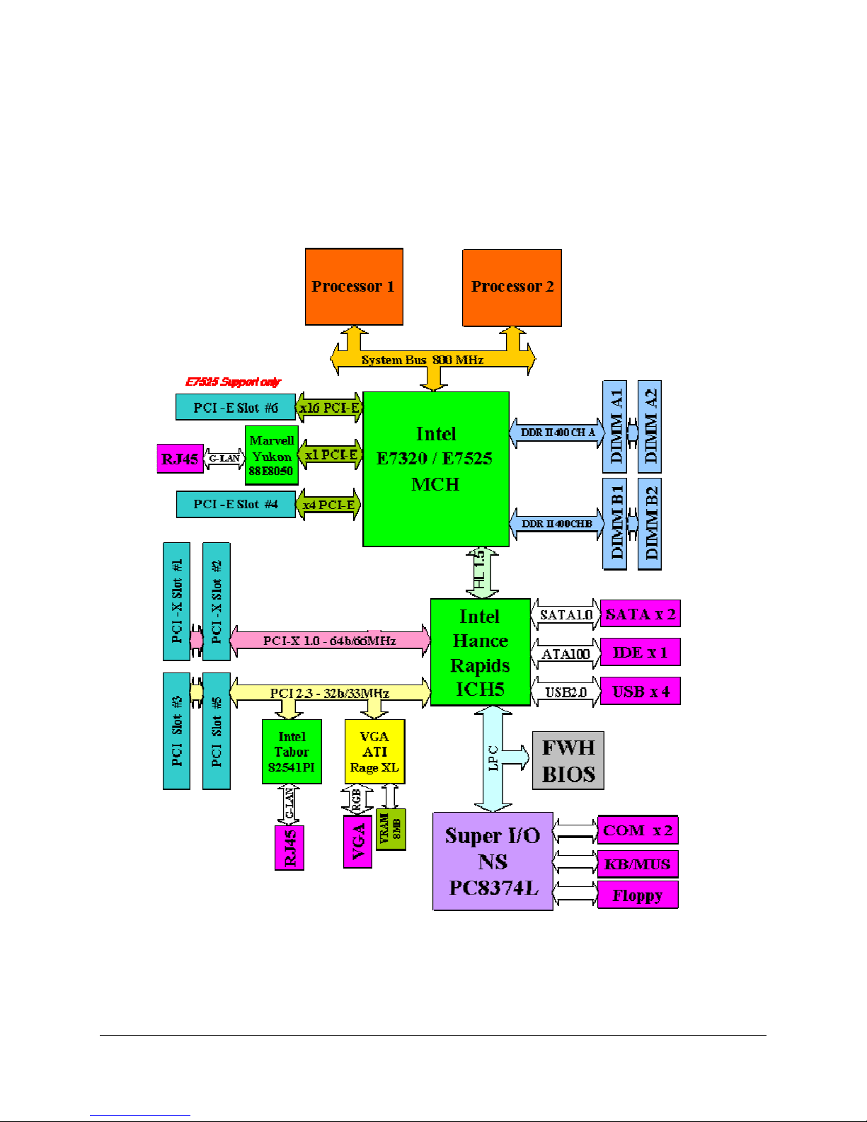
The following figure below shows the functional blocks of the server boards and the plug-in
modules that they support.
Figure 1. Block Diagram of Intel® Server Boards SE7320EP2 and SE7525RP2
Revision 1.0
13
Intel order number D24635-001
Page 14

Intel® Server Board SE7320EP2 / Intel® Server Board SE7525RP2 TPS
Functional Architecture
3. Functional Architecture
This chapter provides a high-level description of the functionality distributed between the
architectural blocks of the Intel® Server Boards SE7320EP2 and SE7525RP2.
3.1 Processor and Memory Subsystem
The Intel® chipset E7320 / E7525 provides a 36-bit address, 64-bit data processor host bus
interface, operating at 800 MHz in the AGTL+ signaling environment. The MCH component of
the chipset provides an integrated memory controller, an 8-bit hub interface, one x8 PCI
Express interface (programmable into separate x 4 interface), and a x16 PCI Express interface
(E7525 MCH only).
The x4 PCI Express interface provides
The interface to x8 PCI Express slot (Lane 0-3)
The interface to Marvell (Lane 4)
The x16 PCI Express interface provides
The interface to x16 PCI Express slot
The 32-bit/33-MHz PCI buses via the 6300ESB ICH
The board directly supports up to 8GB of ECC memory, using four DDR2-400 compliant ECC
DIMMs. The ECC implementation in the MCH can detect and correct single-bit errors (SBE),
detect multiple-bit errors (MBE), and supports Intel® x4 Single Data Device Correction (Intel®
x4 SDDC) feature with x4 DIMMs.
3.1.1 Processor Support
The Intel Server Boards SE7320EP2 and SE7525RP2 support one or two processors in the
604-pin FCPGA package. When two processors are installed, both must be of identical revision,
core voltage, and bus/core speed. When only one processor is installed, it must be in the socket
labeled CPU0. The other socket must be empty. The support circuitry on the server boards
consist of the following:
Dual 604-pin processor sockets supporting 800MHz FSB Intel® Xeon™ processors.
Processor host bus AGTL+ support circuitry.
Table 1. Processor Support Matrix
Processor Family Package Type Frequency Cache Size Front Side Bus Speed
Intel® Xeon™ MPGA604 2.8~3.6GHz 1 MB 800MHz
Intel® Xeon™ MPGA604 3.0~3.6GHz 2 MB 800MHz
Revision 1.0
14
Intel order number D24635-001
Page 15

Intel® Server Board SE7320EP2 / Intel® Server Board SE7525RP2 TPS
Functional Architecture
Notes:
Processors must be populated in sequential order. Processor socket 1 must be
populated before processor socket 2.
The board is designed to provide up to 105A of current per processor. Processors with
higher current requirements are not supported.
No terminator is required in the second processor socket when using a uni-processor
configuration.
In addition to the circuitry described above, the processor subsystem contains the following:
Reset configuration logic
Processor module presence detection logic
Server management registers and sensors
3.1.1.1 Processor VRD
The Intel Server Boards SE7320EP2 and SE7525RP2 have two Voltage Regulator Downs
(VRDs) to support two processors. This is compliant with the VRM 10.1 specification and
provides a maximum of 210 Amps, which is capable of supporting the requirements for two
Intel® Xeon™ processors.
The board hardware must monitor the processor VTTEN (Output enable for VTT) pin for each
processor before turning on the VRD. If the VTTEN pin of the two processors are not identical,
then the Power on Logic will not turn on the VRD.
3.1.1.2 Reset Configuration Logic
The BIOS determines the processor stepping, cache size, and other information through the
CPUID instruction. The requirements are as follows:
All processors in the system must operate at the same frequency, have the same cache
sizes, and same VID. No mixing of product families is supported.
Processors run at a fixed speed and cannot be programmed to operate at a lower or
higher speed.
The processor information is read at every system power-on.
Note: The processor speed is the processor power on reset default value. No manual processor
speed setting options exist either in the form of a BIOS setup option or jumpers.
3.1.1.3 Processor Module Presence Detection
Logic is provided on the server boards to detect the presence and identity of installed
processors. The Power On logic checks the logic and will not turn on the system DC power
unless the VTTENs of both the processors match in a DP configuration.
Revision 1.0
15
Intel order number D24635-001
Page 16
Intel® Server Board SE7320EP2 / Intel® Server Board SE7525RP2 TPS
Functional Architecture
3.1.1.4 Interrupts and APIC
Interrupt generation and notification to the processors is done by the APICs in the 6300ESB ICH
using messages on the front side bus.
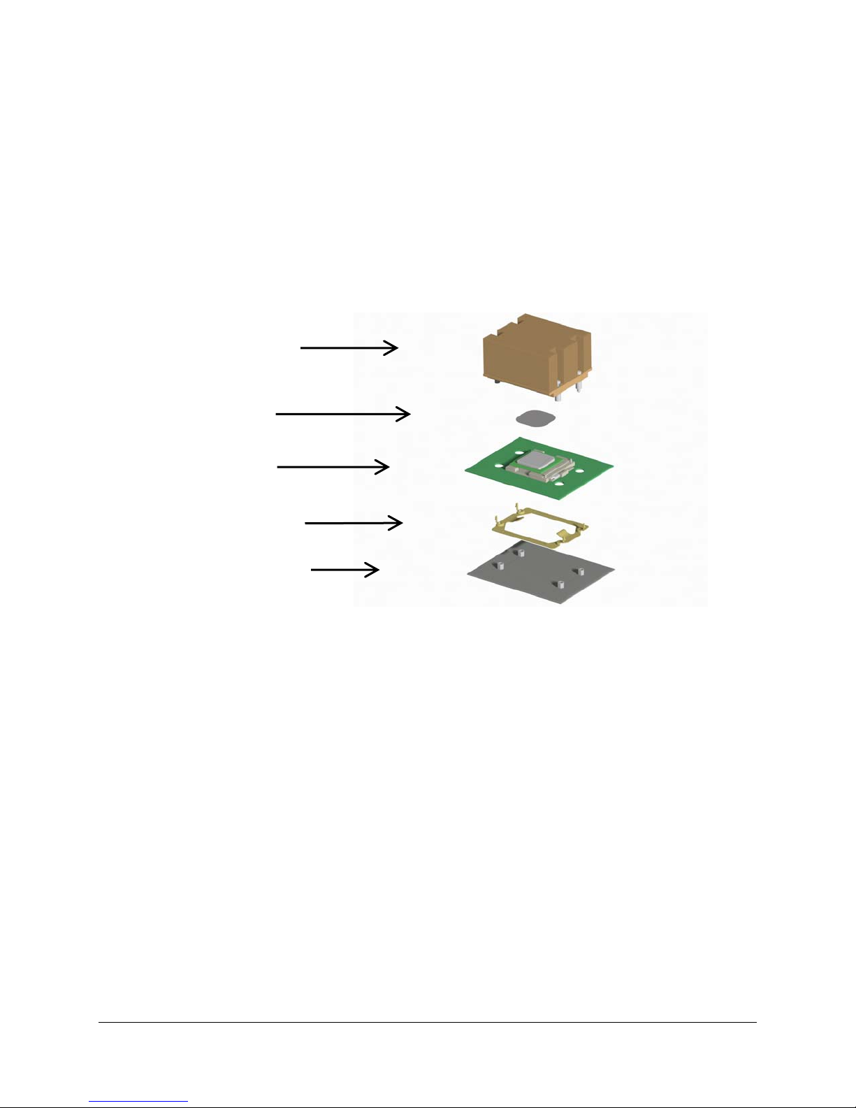
3.1.1.5 Common Enabling Kit (CEK) Design Support
The server boards have been designed to comply with the Intel® Common Enabling Kit (CEK)
processor mounting and thermal solution. The server boards ship from Intel’s factory with a CEK
spring snapped onto the underside of the board, beneath each processor socket. The CEK
spring is removable to allow the use of non-Intel heat sink retention solutions.
Heatsink assembly
with integrated
hardware
TIM
Server Board
CEK Spring
Chassis
Note: When installing either of these server boards into an Intel® Server Chassis SC5300, the
passive heatsink solution (no fan) must be used.
Figure 2. CEK ‘Passive’ Component Stackup
Revision 1.0
16
Intel order number D24635-001
Page 17
Intel® Server Board SE7320EP2 / Intel® Server Board SE7525RP2 TPS
Functional Architecture
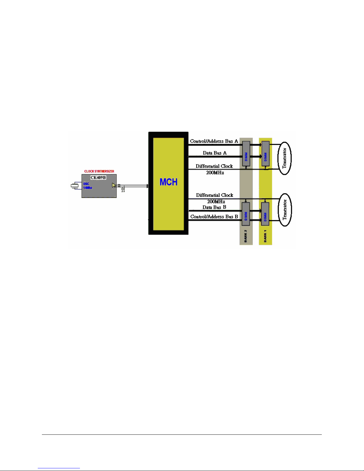
3.1.2 Memory Subsystem
The server boards supports up to four DIMM slots for a maximum memory capacity of 8 GB. The
DIMM organization is x72, which includes eight ECC check bits. The memory interface runs at
400MT/s. The memory controller supports memory scrubbing, single-bit error correction and
multiple-bit error detection and Intel x4 SDDC support with x4 DIMMs. Memory can be
implemented with either single-sided (one row) or double-sided (two row) DIMMs.
The figure below provides a block diagram of the memory sub-system implemented on the
board.
Figure 3. Memory Sub-system Block Diagram
3.1.2.1 Memory DIMM Support
The board supports DDR2-400 compliant ECC DIMMS operating at 400MT/s. Only DIMMs
tested and qualified by Intel or a designated memory test vendor are supported on this board.
All DIMMs are supported by design, but only fully qualified DIMMs will be supported on the
board.
The minimum supported DIMM size is 256MB. Therefore, the minimum main memory
configuration is 1 x 256MB or 256MB. The largest size DIMM supported is a 2GB registered
DDR2-400 ECC DIMM based on 1Gb technology. Therefore, the maximum main memory
configuration is 4 x 2GB or 8GB.
Only registered DDR2-400 compliant, ECC, DDR2 memory DIMMs are supported
ECC single-bit errors (SBE) are corrected and multiple-bit error (MBE) are detected.
The server boards support Intel® x4 SDDC with x4 DIMMs.
The maximum memory capacity is 8GB
The minimum memory capacity is 256MB
Revision 1.0
17
Intel order number D24635-001
Page 18

Intel® Server Board SE7320EP2 / Intel® Server Board SE7525RP2 TPS
Functional Architecture
3.1.2.2 Memory Configuration
The memory interface between the MCH and the DIMMs is 144 bits wide (72 bits for each
bank).
There are two banks of DIMMs, Bank 1 and Bank 2. Bank 1 contains DIMM socket locations 1A
and 1B. Bank 2 contains 2A and 2B. The sockets associated with each bank are located next to
each other and the DIMM socket identifiers are marked on the server board silkscreen, near the
DIMM socket.
For designs that require a lower price point, a single 256MB DIMM can be populated in the
DIMM 1B socket. When a single DIMM is installed, interleaving and Intel x4 SDDC are not
available. Bank 2 will only operate with two DIMMs installed.
The server boards’ signal integrity and cooling are optimized when memory banks are
populated in order. Before populating either DIMM socket in Bank 2, both DIMMs in Bank 1
must be populated. No empty DIMM sockets are allowed between populated DIMMs.
DIMM and memory configurations must adhere to the following:
DDR2-400 ECC, registered DIMM modules
DIMM organization: x72 with ECC
Pin count: 240
DIMM capacity: 256 MB, 512 MB, 1 GB, 2 GB DIMMs
Serial PD: JEDEC Rev 2.0
Voltage options: 1.8 V (VDD/VDDQ)
Interface: SSTL-1.8
Table 2. Memory Bank Labels
Memory DIMM Bank
J18 (DIMM 1A), J16 (DIMM 1B) 1
J21 (DIMM 2A), J20 (DIMM 2B) 2
Revision 1.0
18
Intel order number D24635-001
Page 19
Intel® Server Board SE7320EP2 / Intel® Server Board SE7525RP2 TPS
Functional Architecture
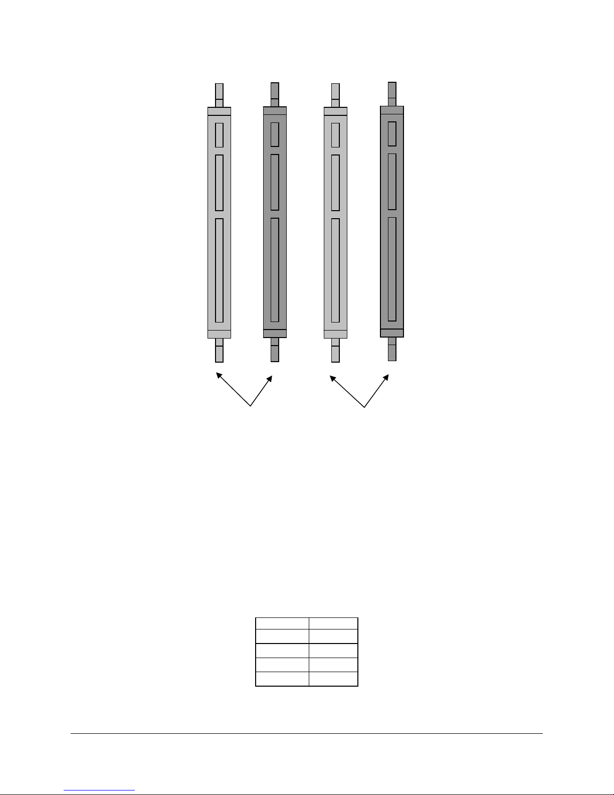
J16 J18 J20 J21
1B 2B 1A 2A
Bank 2
Figure 4. Memory Bank Label Definition
2
3.1.2.3 I
2
The I
C bus is used by the system BIOS to retrieve DIMM information needed to program the
MCH memory registers, which are required to boot the system. The following table provides the
2
I
C addresses for each DIMM slot.
C Bus
Table 3. I2C Addresses for Memory Module SMB
Device Address
DIMM 1A 0xA6
DIMM 1B 0xAE
DIMM 2A 0xA4
DIMM 2B 0xAC
Revision 1.0
19
Intel order number D24635-001
Page 20

Intel® Server Board SE7320EP2 / Intel® Server Board SE7525RP2 TPS
Functional Architecture
3.1.2.4 DRAM ECC
The ECC used for DRAM provides Intel® x4 SDDC technology for x4 SDRAMs. DRAMs that
are x8 use the same algorithm but will not have Intel x4 SDDC technology, since at most only
four bits can be corrected with this ECC.
The method provides more ECC bits so each ECC word can correct more than a single-bit
failure. This is possible because different mathematical algorithms provide multiple-bit
correction with the right number of data bits and ECC bits. For example, a 144-bit ECC word
that consists of 128 data bits and 16 ECC bits can be used to correct up to 4-bit errors within
certain bit fields of data. These four bits must be adjacent, not random. Even though the ratio of
the ECC bits to data bits is the same as the previous example (16/128 vs. 8/64), the longer ECC
word allows for a correction and detection algorithm that is more efficient.
3.2 Intel® E7320 / E7525 Chipset
The Intel Server Boards SE7320EP2 and SE7525RP2 are designed around the Intel E7320 /
E7525 chipset. The chipset provides an integrated I/O bridge and memory controller, and a
flexible I/O subsystem core (PCI Express). This is targeted for multiprocessor systems and
standard high-volume servers. The chipset consists of two components:
MCH: Memory Control Hub. The MCH accepts access requests from the host
(processor) bus and directs those accesses to memory or to one of the PCI buses. The
MCH monitors the host bus, examining addresses for each request. Accesses may be
directed to a memory request queue for subsequent forwarding to the memory
subsystem, or to an outbound request queue for subsequent forwarding to one of the
PCI buses. The MCH also accepts inbound requests from the 6300ESB ICH. The MCH
is responsible for generating the appropriate controls to control data transfer to and from
memory.
6300ESB ICH: The 6300ESB ICH controller has several components. It provides the
interface for a 32-bit/33-MHz PCI bus and the interface for a 64-bit/66MHz PCI-X bus.
The 6300ESB ICH can be both a master and a target on that PCI bus. The 6300ESB
ICH also includes a USB 2.0 controller and an IDE controller. The 6300ESB ICH is also
responsible for much of the power management functions, with ACPI control registers
built in. The 6300ESB ICH also provides a number of GPIO pins and has the LPC bus to
support low speed legacy I/O.
The MCH and 6300ESB ICH chips provide the pathway between processor and I/O systems.
The MCH is responsible for accepting access requests from the host (processor) bus, and
directing all I/O accesses to one of the PCI buses or legacy I/O locations. If the cycle is directed
to one of the PCI Express segments, the MCH communicates with the PCI Express Devices
(add-in card, on board devices) through the PCI Express interface. If the cycle is directed to the
6300ESB ICH, the cycle is output on the MCH’s 8-bit HI 1.5 bus.
The E7320 MCH supports one x8 port configuration PCI Express interface. The E7525MCH
supports one x8 port and one x16 port configuration PCI Express interface. The x8 interface is
capable of logically dividing into separate x4 interface. Each with half the bandwidth of x8
interface and fully compliant to the specification. Maximum theoretical peak bandwidth on each
x8 PCI Express interfaces of 2.5Gb/s in each direction simultaneously, for 5 Gb/s per port.
Revision 1.0
20
Intel order number D24635-001
Page 21

Intel® Server Board SE7320EP2 / Intel® Server Board SE7525RP2 TPS
Functional Architecture
All I/O for the board, including PCI and PC-compatible I/O, is directed through the MCH and
then through the 6300ESB ICH provided PCI buses.
The 6300ESB ICH provides one 32-bit/33-MHz PCI bus, hereafter called P32-A.
The 6300ESB ICH provides one 64-bit/66-MHz PCI-X bus, hereafter called P64-B.
This independent bus structure allows both PCI buses to operate independently and
concurrently, providing additional bandwidth to the system.
3.2.1 MCH Memory Architecture Overview
The MCH supports a 144-bit wide memory sub-system that can support up to 16GB of
DDR2-400 memory, using 4 GB DIMMs. This configuration needs external registers for
buffering the memory address and control signals. The four chip selects are registered inside
the MCH and need no external registers for chip selects.
The memory interface runs at 400MT/s. The memory interface supports a 72-bit or 144-bit wide
memory array. It uses seventeen address lines (BA [2:0] and MA [13:0]) and supports 256 Mb,
512 Mb, 1 Gb DRAM densities. The DDR2 DIMM interface supports memory scrubbing, singlebit error correction, and multiple bit error detection and Intel x4 SDDC with x4 DIMMs.
3.2.1.1 DDR2 Configurations
The DDR2 interface supports up to 8GB of main memory and supports single- and doubledensity DIMMs. DDR2 can be any industry-standard DDR2. The following table shows the
DDR2 DIMM technology supported.
Table 4. Supported DDR2 Technology
Technology Organization DRAM Components / DIMM Row / Column
Address Bits
4M X 8 X 4bks 8 12/10 128Mb
8M X 4 X 4bks 16 12/11
8M X 8 X 4bks 8 13/10 256Mb
16M X 4 X 4bks 16 13/11
16M X 8 X 4bks 8 14/10 512Mb
32M X 4 X 4bks 16 14/11
32M X 8 X 8bks 8 14/10 1Gb
64M X 4 X 8bks 16 14/11
Revision 1.0
21
Intel order number D24635-001
Page 22

Intel® Server Board SE7320EP2 / Intel® Server Board SE7525RP2 TPS
Functional Architecture
3.2.2 Memory Controller Hub (MCH)
The MCH is a 1077-ball FC-BGA device and uses the proven components of previous
generations like the Intel® Xeon™ processor bus interface unit, the hub interface unit, and the
DDR2 memory interface unit. In addition, the MCH incorporates a PCI Express interface. The
PCI Express interface allows the MCH to directly interface with the PXH/PXHD or PCI Express
devices. The MCH also increases the main memory interface bandwidth and maximum memory
configuration with a 144-bit wide memory interface.
The MCH integrates the following main functions:
An integrated high performance main memory subsystem
An PCI Express bus which provides an interface to the PXH/PXHD or PCI Express
devices
A HL 1.5 bus which provides an interface to the 6300ESB ICH
Other features provided by the MCH include the following:
Full support of ECC on the processor bus
Full support of Intel x4 SDDC on the memory interface with x4 DIMMs
Twelve deep in-order queue, two deep defer queue
Full support of registered DDR2-400 ECC DIMMs
Support for 2GB DDR2 memory modules
Memory scrubbing
3.2.3 6300ESB ICH
The 6300ESB ICH is a multi-function device, housed in a 689-pin BGA device, providing a HI
1.5 to PCI bridge, a PCI 32-bit/33MHz interface, a 64-bit/66MHz PCI-X interface, a PCI IDE
interface, a PCI USB controller, and a power management controller. Each function within the
6300ESB ICH has its own set of configuration registers. Once configured, each appears to the
system as a distinct hardware controller sharing the same PCI bus interface.
The primary role of the 6300ESB ICH is to provide the gateway to all PC-compatible I/O devices
and features. The board uses the following the 6300ESB ICH features:
PCI, PCI-X bus interface
LPC bus interface
IDE interface, with Ultra DMA 100 capability
Universal Serial Bus (USB) 2.0 interface
PC-compatible timer/counter and DMA controllers
APIC and 8259 interrupt controller
Power management
System RTC
General purpose I/O (GPIO)
The following are the descriptions of how each supported feature is used on the board.
Revision 1.0
22
Intel order number D24635-001
Page 23

Intel® Server Board SE7320EP2 / Intel® Server Board SE7525RP2 TPS
Functional Architecture
3.2.3.1 PCI Bus P32-A I/O Subsystem
The 6300ESB ICH provides a legacy 32-bit PCI subsystem and acts as the central resource on
this PCI interface. P32-A supports the following embedded devices and connectors:
An ATI Rage XL video controller with 3D/2D graphics accelerator
One Intel
Two 5V expansion slots capable of supporting full-length PCI add-in cards operating at
®
82541PI network controller
33 MHz
3.2.3.2 PCI Bus P64-B I/O Subsystem
The 6300ESB ICH provides a legacy 64-bit PCI-X subsystem and acts as the central resource
on this PCI interface. P64-B supports two 3.3V expansion slots. These support full-length PCI-X
add-in cards operating at 66 MHz.
3.2.3.3 PCI Bus Master IDE Interface
The 6300ESB ICH acts as a PCI-based Ultra DMA 100 IDE controller that supports
programmed I/O transfers and bus master IDE transfers. The 6300ESB ICH supports two IDE
channels, supporting two drives each (drives 0 and 1). The Intel Server Boards SE7320EP2 and
SE7525RP2 implement one 40-pin IDE connector to access the IDE functionality.
The IDE interface supports Ultra DMA 100 Synchronous DMA Mode transfers on the 40-pin
connector.
3.2.3.4 USB Interface
The 6300ESB ICH contains one EHCI USB 2.0 controller and four USB ports. The USB
controller moves data between the main memory and up to four USB connectors. All ports
function identically and with the same bandwidth. The Server Boards SE7320EP2 and
SE7525RP2 implement four ports on the board.
The server boards provide two external USB ports on the back. The dual-stack USB connector
is located within the standard ATX I/O panel area next to the keyboard and mouse housing. The
USB specification defines the external connectors.
The third and fourth USB ports are optional and can be accessed by cabling from an internal 9pin connector on the server boards to an external USB port either at the front or the rear of a
chassis.
3.2.3.5 Two port SATA Interface
The 6300ESB ICH contains one SATA controller and two SATA ports. The data transfer rates
up to 150Mbyte/s. Alternate Device ID and RAID Class Code options support Soft RAID.
3.2.3.6 Compatibility Interrupt Control
The 6300ESB ICH provides the functionality of two 82C59 PIC devices for ISA-compatible
interrupt handling.
Revision 1.0
23
Intel order number D24635-001
Page 24

Intel® Server Board SE7320EP2 / Intel® Server Board SE7525RP2 TPS
Functional Architecture
3.2.3.7 APIC
The 6300ESB ICH integrates an I/O APIC capability with 24 interrupts.
3.2.3.8 General Purpose Input and Output Pins
The 6300ESB ICH provides a number of general purpose input and output pins. Many of these
pins have alternate functions, and thus all are not available. The following table lists the GPI
and GPO pins used on the board and gives a brief description of their function.
Table 5. 6300ESB ICH GPIO Usage Table
Pin Name (Powe
Well)
GPIO0/PXREQ2# Core Input HR_PAREQ2_N PXREQ2#
GPIO1/PXREQ3# Core Input HR_PAREQ3_N PXREQ3#
GPIO2/PIRQE# Core Input PCI_PIRQE_N PIRQE#
GPIO3/PIRQF# Core Input PCI_PIRQF_N PIRQF#
GPIO4/PIRQG# Core Input PERR_LOG Parity Error Log
GPIO5/PIRQH# Core Input PCI_PIRQH_N PIRQH#
GPIO6 Core Input SKU_VER_ID1 SKU Version ID 1
GPIO7 Core Input MCHPME_N MCH Power Management Event
GPIO8 Resume Input FP_NMI_BTN_N Input: NMI Button
GPIO11/SMBALERT# Resume Input PS_ALERT_N SM Bus alert from power supply
GPIO12 Resume Input MANUF_DET_N Manufacture Mode detect
GPIO13 Resume Input SIO_SMI_N SMI# source from Super I/O
GPIO16/PXGNT2# Core Output HR_PAGNT2_N PXGNT2#
GPIO17/PXGNT3# Core Output HR_PAGNT3_N PXGNT3#
GPIO18 Core Output TP_GPIO_FAN_N Unused
GPIO19 Core Output GPIO_RST_N Generate a hardware reset
GPIO20 Core Output Reserved Reserved
GPIO21 Core Output HR_FLASH_WP_N Active Low to enable flash BOM Write
GPIO23 Core Output POST_STATUS_N Active Low to report POST status
GPIO24 Resume Input/Output DIMM_FRULED-A1_N Output: DIMM FRU LED for 1A
GPIO25 Resume Input/Output DIMM_FRULED-A2_N Output: DIMM FRU LED for 2A
GPIO27 Resume Input/Output NC Unused
GPIO28 Resume Input/Output NC Unused
GPIO32/WDT_TOUT# Core Input/Output SKU_VER_ID2 Input: SKU Version ID 1
GPIO33/PXIRQ0# Core Input/Output HR_PAIRQA_N PXIRQ0#
GPIO34/PXIRQ1# Core Input/Output HR_PAIRQB_N PXIRQ1#
GPIO35/PXIRQ2# Core Input/Output HR_PAIRQC_N PXIRQ2#
GPIO36/PXIRQ3# Core Input/Output HR_PAIRQD_N PXIRQ3#
GPIO37 Core Input/Output PASSWORD_CLEAR_N Input: Password clear selection
GPIO38 Core Input/Output BIOS_RCVR_N Input: BIOS Recover boot selection
GPI / GPO /
Function
Signal Name Function Description
protect
L: Clear Password; H: Normal
L: Recovery; H: Normal
Revision 1.0
24
Intel order number D24635-001
Page 25

Intel® Server Board SE7320EP2 / Intel® Server Board SE7525RP2 TPS
Functional Architecture
Pin Name (Powe
Well)
GPIO39 Core Input/Output DIS_VGA_N Output: Active Low to disable on
GPIO40 Core Input/Output CMOS_CLEAR_N Input: CMOS Clear selection
GPIO41 Core Input/Output SKU_VER_ID0 Input: SKU Version ID 0
GPIO42 Core Input/Output IDE_PRI_CBLSNS Input: Primary IDE cable type sense
GPIO43 Core Input/Output MROMB_PRESENT_N Input: ZCR card present
GPIO56 Resume Output KNI_DISABLE_N Output: Active Low to disable on
GPIO57 Resume Output YKN_DIS_N_A Output: Active Low to disable on
GPI / GPO /
Function
Signal Name Function Description
board VGA
L: Clear CMOS; H: Normal
L: 80 conductor cable; H: 40
conductor cable
board 82541PI
board 88E8050
3.2.3.9 Power Management
One of the embedded functions of the 6300ESB ICH is a power management controller. This is
used to implement ACPI-compliant power management features. The server boards support
sleep states S0, S1, S4, and S5.
3.3 Super I/O
The National Semiconductor* 8374L Super I/O device contains all of the necessary circuitry to
control two serial ports, one parallel port, floppy disk, PS/2-compatible keyboard and mouse and
hardware monitor controller. The server boards implement the following features:
GPIOs
Two serial ports
Floppy
Keyboard and mouse
Local hardware monitoring
Wake up control
System health support
Revision 1.0
25
Intel order number D24635-001
Page 26

Intel® Server Board SE7320EP2 / Intel® Server Board SE7525RP2 TPS
Functional Architecture
3.3.1 GPIOs
The Super I/O provides a number of general-purpose input/output pins that the server boards
utilize. The following table identifies the pin and the signal name used in the schematics:
Table 6. Super I/O* GPIO Usage Table
Pin Power Pin
Number
GPIOE00/SWD Standby 103 SIO_TEMP_SENSOR I/O: LMPCIF
GPIOE01/FANTACH3 Standby 104 FAN_TACH_REAR1 Input: Rear fan tach 1
GPIOE02/FANTACH4 Standby 105 FAN_TACH_6PIN Input: 6-pin fan tach
GPIOE03/FANPWM1 Standby 106 FANPWM_FRONT1 Output: Front fan
GPIOE04/FANPWM2 Standby 108 FAN_PWM_REAR1 Output: Rear fan
GPIOE05/FANPWM3 Standby 109 FAN_PWM_6PIN Output: 6-pin fan
GPIOE06/FANTACH1 Standby 111 FAN_TACH_FRONT1 Input: Front fan tach 1
GPIOE07/FANTACH2 Standby 112 FAN_TACH_FRONT2 Input: Front fan tach 2
GPIOE00/RI2_N/IRTX VDD3 118 SIO_RI2_N COM2
GPIOE01/SIN2/RI2* VDD3 119 SIO_SIN2 COM2
GPIOE02/SOUT2/IRRX VDD3 120 SIO_SOUT2 COM2
GPIOE03/DSR2_N_SIN2 VDD3 121 SIO_DSR2_N COM2
GPIOE04/CTS2_N/DSR2* VDD3 124 SIO_CTS2_N COM2
GPIOE05/DCD2_N/CTS2* VDD3 126 SIO_DCD2_N COM2
GPIOE06/IRRX/DTR_BOUT2 VDD3 127 RISER_PRESENT2 Input: riser card
GPIOE07/IRTX/DCD2* VDD3 128 2U_RISER_DETECT Input: 2U riser card
GPIOE10/5V_DDCSDA Standby 116 HR_SMB_P5VSB_DAT SMB
GPIOE11/5V_DDCSCL Standby 114 HR_SMB_P5VSB_CLK SMB
GPIOE12/CC_DDCSDA Standby 115 HR_SMB_3V3SB_DAT SMB
GPIOE13/CC_DDCSCL Standby 113 HR_SMB_3V3SB_CLK SMB
GPIOE12/PCIRST_OUT2_N Standby 74 PCIRST_N_R Output: PCIRST
GPIOE13 Standby 75 PCIE_WAKE_N Input: PCIE-Wake up
GPIOE14 Standby 101 PME_N Input: PCI PME#
GPIOE16 Standby 100 DIMM_FRULED_B1_N Output: DIMM FRU
GPIOE17 Standby 80 PME_PCIX_N Input: PCI-X PME#
GPO11/VsbStrap1 Standby 117 SIO_VSBSTRAP1 SIO Strapping
GPO12/RTS2_N/SOUT2/VddStrap1 VDD3 122 SIO_RTS2_N COM2
GPO13/DTR_BOUT2/RTS2_N/VddStrap2 VDD3 125 SIO_DTR2_N COM2
GPIO15 Standby 91 DIMM_FRULED_B2_N Output: DIMM FRU
Signal Name Function Description
PWM 1
PWM 1
PWM
present
detect
buffer
signal
LED for 1B
LED for 2B
Revision 1.0
26
Intel order number D24635-001
Page 27

Intel® Server Board SE7320EP2 / Intel® Server Board SE7525RP2 TPS
Functional Architecture
3.3.2 Serial Ports
The board provides two serial ports, an external serial port, and an internal serial header. The
following sections provide details on the use of the serial ports.
3.3.2.1 Serial A
Serial A is a standard DB9 interface located at the rear I/O panel of the server boards, to the left
of the video connector below the parallel port connector. Serial A is designated by as “Serial A”
on the silkscreen. The reference designator is J4.
3.3.2.2 Serial B
Serial B is an optional port, accessed through a 9-pin internal header. A standard DH-10 to DB9
cable can be used to direct serial B to an external connector on any given chassis. The serial B
interface follows the standard RS232 pinout. The server boards have a “Serial_B” silkscreen
label next to the connector and is located beside the PCI-X slot 1 connector.
3.3.2.3 Floppy Disk Controller
The floppy disk controller (FDC) in the Super I/O is functionally compatible with floppy disk
controllers in the DP8473 and N844077. All FDC functions are integrated into the Super I/O
including analog data separator and 16-byte FIFO. The server boards provide a standard 34-pin
interface for the floppy disk controller.
3.3.2.4 Keyboard and Mouse
Two external PS/2 ports, located on the back of the server boards, provide access to the
keyboard and mouse functions.
3.3.2.5 Wake-up Control
The Super I/O contains functionality that allows various events to control the power-on and
power-off the system.
3.4 BIOS Flash
The board incorporates an Intel® FWH flash memory component. The 82802AC is a highperformance 8-megabit memory component and non-volatile storage space. The flash device is
connected through the LPC interface of 6300ESB.
Revision 1.0
27
Intel order number D24635-001
Page 28
Intel® Server Board SE7320EP2 / Intel® Server Board SE7525RP2 TPS
Functional Architecture
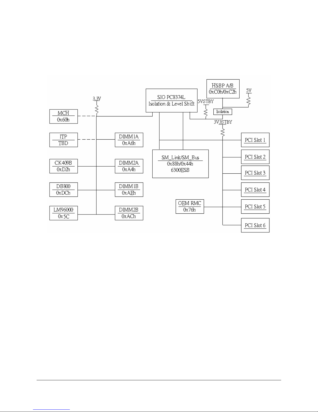
3.5 SM Bus Block Diagram
See below for the SM Bus block diagram and device addresses.
Figure 5. Intel® Server Boards SE7320EP2 and SE7525RP2 SMBUS Block Diagram
Revision 1.0
28
Intel order number D24635-001
Page 29

Intel® Server Board SE7320EP2 / Intel® Server Board SE7525RP2 TPS
Clock Generation and Distribution
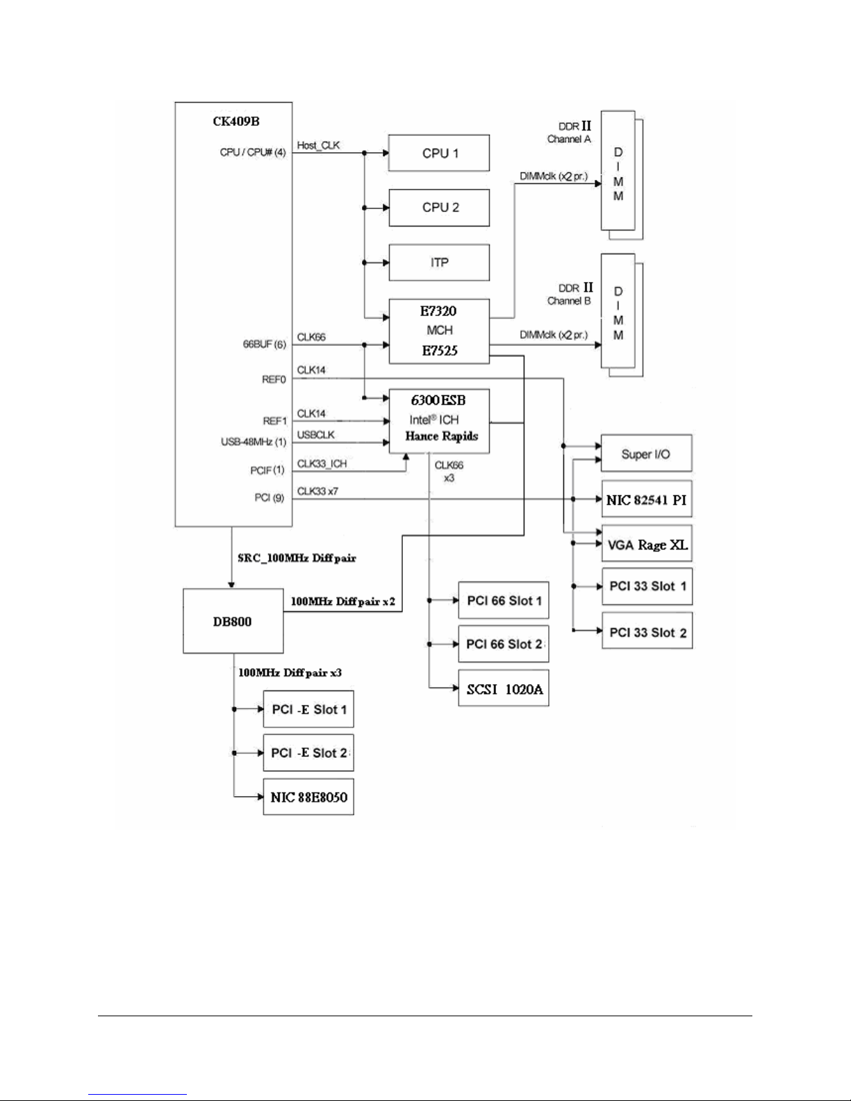
4. Clock Generation and Distribution
All buses on the Intel Server Boards SE7320EP2 / SE7525RP2 operate using synchronous
clocks. Clock synthesizer/driver circuitry on the server board generates clock frequencies and
voltage levels as required, including the following:
200 MHz at 0.7V current-mode: For processor 0, processor 1, debug port and MCH
66 MHz at 3.3 V logic levels: For MCH, 6300ESB ICH
48 MHz at 3.3V logic levels: For 6300ESB ICH
33 MHz at 3.3V logic levels: For 6300ESB ICH, PCI connector, Super I/O
14.318 MHz at 2.5 V logic levels: For 6300ESB ICH , Super I/O and video
The following figure illustrates clock generation and distribution on the board.
Revision 1.0
29
Intel order number D24635-001
Page 30
Intel® Server Board SE7320EP2 / Intel® Server Board SE7525RP2 TPS
Clock Generation and Distribution
Figure 6. Intel® Server Boards SE7320EP2 and SE7525RP2 Clock Distribution Diagram
Revision 1.0
30
Intel order number D24635-001
Page 31

Intel® Server Board SE7320EP2 / Intel® Server Board SE7525RP2 TPS
PCI I/O Subsystem
5. PCI I/O Subsystem
5.1 PCI Subsystem
The primary I/O buses for the server boards SE7320EP2 and SE7525RP2 are PCI, PCI
Express, and PCI-X, with three independent PCI bus segments. The PCI buses comply with the
PCI Local Bus Specification, Revision 2.3. The P32-A bus and the P64-B segment are directed
through the 6300ESB ICH and the two PCI Express (x4 and x16) buses are directed through the
MCH. The table below lists the characteristics of the three PCI bus segments.
Table 7. PCI Bus Segment Characteristics
PCI Bus Segment Voltage Width Speed Type PCI I/O Card Slots
PCI 5V 32 bits 33MHz Slot 3 Slot 5
PCI-X 3.3V 64 bits 66MHz Slot 1; Slot 2
PCI Express (x8) 3.3 4 lanes 100MHz Slot 4
PCI Express (x16) 3.3 16 lanes 100MHz Slot 6 (E7525 chipset only)
5.1.1 P32-A: 32-bit/33-MHz PCI Subsystem
All 32-bit/33-MHz PCI I/O for the board is directed through the 6300ESB ICH. The 32-bit/33MHz PCI segment created by the 6300ESB ICH is known as the P32-A segment. The P32-A
segment supports the following embedded devices and connectors:
One 10/100/1000 Network Interface Controller: Intel
2D/3D Graphics Accelerator: ATI* Rage* XL Video Controller
Two 5V, 32-bit PCI slots
The video controller and the NIC are each allocated a GPIO to disable the device.
5.1.1.1 Device IDs (IDSEL)
Each device under the PCI hub bridge has its IDSEL signal connected to one bit of AD[31:16],
which acts as a chip select on the PCI bus segment in configuration cycles. This determines a
unique PCI device ID value for use in configuration cycles. The following table shows the bit to
which each IDSEL signal is attached for P32-A devices and the corresponding device
description.
Table 8. P32-A Configuration IDs
IDSEL Value Device
18 Video
19 Intel 82541PI
20 PCI Slot 3 (32b/33M)
21 PCI Slot 5 (32b/33M)
®
82541PI Fast Ethernet Controller.
Revision 1.0
31
Intel order number D24635-001
Page 32

Intel® Server Board SE7320EP2 / Intel® Server Board SE7525RP2 TPS
PCI I/O Subsystem
5.1.1.2 P32-A Arbitration
P32-A supports four PCI devices: the 6300ESB ICH and four PCI bus masters (one NIC, two
PCI slots, and one ATI* Rage* XL video controller). All PCI masters must arbitrate for PCI
access, using resources supplied by the 6300ESB ICH. The host bridge PCI interface
(6300ESB ICH) arbitration lines REQx* and GNTx* are a special case in that they are internal to
the host bridge. The following table defines the arbitration connections.
Table 9. P32-A Arbitration Connections
Baseboard Signals Device
PCI REQ0_N/GNT0_N Video ATI* Rage* XL
PCI REQ1_N/GNT1_N NIC Intel 82541PI
PCI REQ2_N/GNT2_N PCI Slot 3 (32b/33M)
PCI REQ3_N/GNT3_N PCI Slot 5 (32b/33M)
5.1.2 P64-B 66-MHz PCI-X Subsystem
One 64-bit PCI-X bus segment is directed through the 6300ESB ICH. This PCI-X segment, P64B, provides two 3.3V 64-bit PCI-X slots capable of 66MHz operation and supporting full-length
PCI cards. The P64-B segment supports two 3.3V, 64-bit PCI slots.
5.1.2.1 Device IDs (IDSEL)
Each device under the PCI-X hub bridge has its IDSEL signal connected to one bit of AD[31:16],
which acts as a chip select on the PCI bus segment in configuration cycles. This determines a
unique PCI device ID value for use in configuration cycles. The following table shows the bit to
which each IDSEL signal is attached for P64-B devices and corresponding device description.
Table 10. P64-B Configuration IDs
IDSEL Value Device
19 PCI-X Slot 2 (64b/66M, Riser, RADIOS)
18 PCI-X Slot 1 (64b/66M)
Revision 1.0
32
Intel order number D24635-001
Page 33

Intel® Server Board SE7320EP2 / Intel® Server Board SE7525RP2 TPS
PCI I/O Subsystem
5.1.2.2 P64-B Arbitration
P64-B supports two PCI masters, one on each PCI-X slot. All PCI masters must arbitrate for
PCI access using resources supplied by the 6300ESB ICH. The host bridge PCI interface
(6300ESB ICH) arbitration lines REQx* and GNTx* are a special case in that they are internal to
the host bridge. The following table defines the arbitration connections.
Table 11. P64-B Arbitration Connections
Server Board Signals Device
PCIX REQ1_N/GNT1_N PCI Slot 2 (64b/66M)
PCIX REQ0_N/GNT0_N PCI Slot 1 (64b/66M)
5.1.3 PCI Express x8
The PCI Express x8 interface can be configured as two independent x4 interfaces. On the Intel
Server Boards SE7320EP2 and SE7525RP2, Lanes 0-3 are connected to a x8 PCI Express
connector and Lane 4 is connected to Marvell 88E8050. Lanes 5-7 are terminated.
Table 12. PCI Express x8 Connections
Lane Device
Lane 0-3 Slot 4 (PCI Express)
Lane 4 Marvell 88E8050
Lane 5-7 NC
5.1.4 PCI Express x16 (E7525 MCH support only)
The PCI Express x16 interface is connected to a x16 PCI Express connector. This connector is
supported on the Intel Server Board SE7525RP2 board only.
Table 13. PCI Express x16 (Port B) Connections
Lane Device
Lane 8-23 Slot 6 (PCI Express)
Revision 1.0
33
Intel order number D24635-001
Page 34

Intel® Server Board SE7320EP2 / Intel® Server Board SE7525RP2 TPS
PCI I/O Subsystem
5.2 Video Controller
The server boards provide an ATI Rage XL PCI graphics accelerator, along with 8MB of video
SDRAM and support circuitry for an embedded SVGA video subsystem. The ATI Rage XL chip
contains a SVGA video controller, clock generator, 2D and 3D engine, and RAMDAC in a 272pin PBGA. One 2Mx32-bit SDRAM chip provides 8MB of video memory.
The SVGA subsystem supports a variety of modes, up to 1600 x 1200 resolution in
8/16/24/32 bpp modes under 2D, and up to 1024 x 768 resolution in 8/16/24/32 bpp modes
under 3D. It supports both CRT and LCD monitors with up to 100Hz vertical refresh rate.
The server boards provide a standard 15-pin VGA connector at the rear of the system in the
standard ATX I/O opening area. The video controller is disabled by default in BIOS Setup when
an add-in card video adapter is detected in either the AGP or PCI slots. As an option, the video
controller can be set to support dual-monitor mode when an AGP adapter is detected. In this
circumstance, the onboard controller acts as the primary video controller and the AGP adapter
becomes the secondary adapter under an operating system that supports this functionality.
5.2.1 Video Modes
The ATI Rage XL chip supports all standard IBM VGA modes. The following table shows the
2D/3D modes supported for both CRT and LCD. The table specifies the minimum memory
requirement for various display resolution, refresh rates, and color depths.
Table 14. Video Modes
2D Video Mode Support 2D Mode Refresh Rate (Hz)
8 bpp 16 bpp 24 bpp 32 bpp
640x480 60, 72, 75, 90, 100 Supported Supported Supported Supported
800x600 60, 70, 75, 90, 100 Supported Supported Supported Supported
1024x768 60, 72, 75, 90, 100 Supported Supported Supported Supported
1280x1024 43, 60 Supported Supported Supported Supported
1280x1024 70, 72 Supported – Supported Supported
1600x1200 60, 66 Supported Supported Supported Supported
1600x1200 76, 85 Supported Supported Supported –
3D Mode Refresh Rate (Hz) 3D Video Mode Support with Z Buffer Enabled
640x480 60,72,75,90,100 Supported Supported Supported Supported
800x600 60,70,75,90,100 Supported Supported Supported Supported
1024x768 60,72,75,90,100 Supported Supported Supported Supported
1280x1024 43,60,70,72 Supported Supported – –
1600x1200 60,66,76,85 Supported – – –
3D Mode Refresh Rate (Hz) 3D Video Mode Support with Z Buffer Disabled
640x480 60,72,75,90,100 Supported Supported Supported Supported
800x600 60,70,75,90,100 Supported Supported Supported Supported
1024x768 60,72,75,90,100 Supported Supported Supported Supported
1280x1024 43,60,70,72 Supported Supported Supported –
1600x1200 60,66,76,85 Supported Supported – –
Revision 1.0
34
Intel order number D24635-001
Page 35

Intel® Server Board SE7320EP2 / Intel® Server Board SE7525RP2 TPS
PCI I/O Subsystem
5.2.2 Video Memory Interface
The memory controller subsystem of the ATI Rage XL arbitrates requests from direct memory
interface, the VGA graphics controller, the drawing coprocessor, the display controller, the video
scalar, and hardware cursor. Requests are serviced in a way that ensures display integrity and
maximum CPU/coprocessor drawing performance.
The board supports an 8MB (512K x 32-bit x four banks) SDRAM device for video memory.
5.2.3 Host Bus Interface
The ATI Rage XL supports a PCI33 MHz bus. The following diagram shows the signals for the
PCI interface:
PCICLK CPUCLK
AD[31..0] AD[31..0]
C/BE#[3..0] C/BE[3..0]
PAR PAR
FRAME# FRAME#
IRDY# IRDY#
IDSEL IDSEL
PCIRST# RESET#
TRDY# TRDY#
STOP# STOP#
INTR# INTR#
DEVSEL# D EVSEL#
REQ# REQ#
GNT# GNT#
Figure 7. Video Controller PCI Bus Interface
Revision 1.0
35
Intel order number D24635-001
Page 36

Intel® Server Board SE7320EP2 / Intel® Server Board SE7525RP2 TPS
PCI I/O Subsystem
5.3 Network Interface Controller (NIC)
The server boards SE7320EP2 and SE7525RP2 support one 10Base-T / 100Base / 1000BaseT network interface controller (NIC) based on the Intel® 82541PI controller (NIC 2) and one
gigabit network interface controller based on the Marvell* 88E8050 controller (NIC 1).
The Intel 82541PI Gigabit Ethernet is a single, compact component with an integrated Gigabit
Ethernet Media Access Control (MAC) and physical layer (PHY) functions. For desktop,
workstation and mobile PC network designs with critical space constraints, the Intel 82541PI
allows for a Gigabit Ethernet implementation in a very small area that is footprint compatible
with current generation 10/100 Mbps Fast Ethernet designs. The Intel 82541PI integrates fourth
generation gigabit MAC design with fully integrated, physical layer circuitry to provide a standard
IEEE 802.3 Ethernet interface for 1000BASE-T, 100BASE_TX, and 10BASE-T applications
(802.3, 802.3u, and 802.3ab). The controller is capable of transmitting and receiving data at
rates of 1000 Mbps, 100 Mbps, or 10 Mbps. In addition to managing MAC and PHY layer
functions, the controller provides a 32-bit wide direct Peripheral Component Interconnect (PCI)
2.3 compliant interface capable of operating at 33 or 66MHz.
The single-chip PCI Express based 88E8050 device integrates the Marvell Gigabit PHY with the
Marvell Gigabit MAC and SERDES cores, delivering an ultra-small form factor and high
performance. The 88E8050 device is compliant with the PCI Express 1.0a specification. Offered
in a 9 x 9 mm, 64-pin QFN package, the 88E8050 reduces board space required for Gigabit
LOM implementation.
5.3.1 NIC Connector and Status LEDs
The NICs drive two LEDs located on each network interface connector. For each NIC
connector, the green LED indicates network connection when on, and Transmit/Receive activity
when blinking. The yellow LED indicates 1000-Mbps operation when lit, the green LED indicates
100-Mbps operation when lit and 10-Mbps when off.
5.4 Interrupt Routing
The board interrupt architecture accommodates both PC-compatible PIC mode and APIC mode
interrupts through use of the integrated I/O APICs in the 6300ESB ICH.
5.4.1 Legacy Interrupt Routing
For PC-compatible mode, the 6300ESB ICH provides two 82C59-compatible interrupt
controllers. The two controllers are cascaded with interrupt levels 8-15 entering on level 2 of the
primary interrupt controller (standard PC configuration). A single interrupt signal is presented to
the processors, to which only one processor will respond for servicing. The 6300ESB ICH
contains configuration registers that define which interrupt source logically maps to I/O APIC
INTx pins.
The 6300ESB ICH handles both PCI and IRQ interrupts. The 6300ESB ICH translates these to
the APIC bus. The numbers in the table below indicate the 6300ESB ICH PCI interrupt input pin
to which the associated device interrupt (INTA, INTB, INTC, INTD, INTE, INTF, INTG, INTH for
PCI bus and PXIRQ0, PXIRQ1, PXIRQ2, PXIRQ3 for PCI-X bus) is connected. The 6300ESB
ICH I/O APIC exists on the I/O APIC bus with the processors.
Revision 1.0
36
Intel order number D24635-001
Page 37

Intel® Server Board SE7320EP2 / Intel® Server Board SE7525RP2 TPS
PCI I/O Subsystem
Table 15. PCI AND PCI-X Interrupt Routing/Sharing
Interrupt INT A INT B INT C INT D
Video PIRQB
82541P1 PIRQA
PCI Slot 3 (PCI 32b/33M) PIRQF PIRQD PIRQB PIRQH
PCI Slot 5 (PCI 32b/33M) PIRQE PIRQB PIRQH PIRQD
LSI 1020A PXIRQ3
PCI Slot 2 (64b/66M) PXIRQ1 PXIRQ2 PXIRQ3 PXIRQ0
PCI Slot 1 (64b/66M) PXIRQ0 PXIRQ1 PXIRQ2 PXIRQ3
5.4.2 APIC Interrupt Routing
For APIC mode, the interrupt architecture incorporates three Intel I/O APIC devices to manage and
broadcast interrupts to local APICs in each processor. The Intel I/O APICs monitor each interrupt on
each PCI device, including PCI slots, in addition to the ISA compatibility interrupts IRQ(0-15).
When an interrupt occurs, a message corresponding to the interrupt is sent across a three-wire
serial interface to the local APICs. The APIC bus minimizes interrupt latency time for
compatibility interrupt sources. The I/O APICs can also supply greater than 16 interrupt levels to
the processor(s). This APIC bus consists of an APIC clock and two bidirectional data lines.
5.4.2.1 Legacy Interrupt Sources
The table below recommends the logical interrupt mapping of interrupt sources on the board.
The actual interrupt map is defined using configuration registers in the 6300ESB ICH.
Table 16. Interrupt Definitions
ISA Interrupt Description
INTR Processor interrupt.
NMI NMI to processor.
IRQ0 System timer
IRQ1 Keyboard interrupt.
IRQ2 Slave PIC
IRQ3 Serial port 1 or 2 interrupt from Super I/O device, user-configurable.
IRQ4 Serial port 1 or 2 interrupt from Super I/O device, user-configurable.
IRQ5 Parallel Port / Generic
IRQ6 Floppy disk.
IRQ7 Parallel Port / Generic
IRQ8_L Active low RTC interrupt.
IRQ9 SCI*
IRQ10 Generic
IRQ11 Generic
IRQ12 Mouse interrupt.
IRQ13 Floaty processor.
IRQ14 Compatibility IDE interrupt from primary channel IDE devices 0 and 1.
IRQ15
SMI* System Management Interrupt. General purpose indicator sourced by the 6300ESB ICH to the
processors.
Revision 1.0
37
Intel order number D24635-001
Page 38

Intel® Server Board SE7320EP2 / Intel® Server Board SE7525RP2 TPS
PCI I/O Subsystem
5.4.3 Serialized IRQ Support
The Server Boards SE7320EP2 and SE7525RP2 supports a serialized interrupt delivery
mechanism. Serialized Interrupt Requests (SERIRQ) consists of a start frame, a minimum of 17
IRQ / data channels, and a stop frame. Any slave device in the quiet mode may initiate the start
frame. While in the continuous mode, the start frame is initiated by the host controller.
6300ESB
IOAPIC 0
IRQ0
IRQ1
IRQ2
IRQ3
IRQ4
IRQ5
IRQ6
IRQ7
IRQ8
IRQ9
IRQ10
IRQ11
IRQ12
IRQ13
IRQ14
IRQ15
IRQ16
IRQ17
IRQ18
6300
ESB
6300ESB
8259PIC
X8
connector
and Marvell*
88E8050
X16
Connector
-
X16 PCI Express interface
(Supported by E7525 chipset only)
MCH
INTR
CPU1
INTR
CPU2
Revision 1.0
38
Figure 8. Interrupt Routing Diagram
Intel order number D24635-001
Page 39

Intel® Server Board SE7320EP2 / Intel® Server Board SE7525RP2 TPS
A
A
,
A
A
A
A
PCI I/O Subsystem
Super I/O
Serialized IRQ Interface
6300ESB ICH Interrupt
Routing PCI Interface
82541PI INT
Video INTA, Slot 3 INTC, Slot 5 INTB
Slot 3 INTB, Slot 5 INTD
Slot 5 INT
Slot 3 INT
Slot 3 INTD, Slot 5 INTC
Slot 1 INTA, Slot 2 INT
Slot 1 INTB, Slot 2 INT
Slot 1 INTC, Slot 2 INTB
Slot 1 INTD Slot 2 INTC
LSI1020A INT
PXIRQ0
PXIRQ1
PXIRQ2
PXIRQ3
PCI-X
interface
Revision 1.0
Figure 9. Interrupt Routing Diagram
39
Intel order number D24635-001
Page 40

Intel® Server Board SE7320EP2 / Intel® Server Board SE7525RP2 TPS
PCI I/O Subsystem
5.5 PCI Error Handling
The PCI bus defines two error pins, PERR# and SERR#, for reporting PCI parity errors and
system errors, respectively. In the case of PERR#, the PCI bus master has the option to retry
the offending transaction, or to report it using SERR#. All other PCI-related errors are reported
by SERR#. SERR# is routed to NMI if enabled by BIOS.
Revision 1.0
40
Intel order number D24635-001
Page 41

Intel® Server Board SE7320EP2 / Intel® Server Board SE7525RP2 TPS
g
BIOS
6. BIOS
6.1 BIOS Architecture
The Basic Input/Output System (BIOS) is implemented as firmware that resides in the Flash
ROM. It provides hardware-specific initialization algorithms and standard PC-compatible basic
input/output (I/O) services, and standard Intel® Server Board features. The Flash ROM also
contains firmware for certain embedded devices. These images are supplied by the device
manufacturers and are not specified in this document.
The system BIOS includes the following components:
IA-32 Core: The IA-32 core contains standard services and components such as the PCI
Resource manager, ACPI support, POST, and runtime functionality.
Processor Microcode: BIOS includes microcode for the latest processors.
Option ROMs: BIOS includes option ROMs to enable on-board devices during boot.
6.1.1 BIOS Identification String
The BIOS Identification string is used to uniquely identify the revision of the BIOS being used on
the system. The string is formatted as illustrated in the following figure.
BoardId.OEMID.BuildType.Major.Minor.BuildID.BuildDateTime.Mod
Build Date and time in
MMDDYYYYHHMM format
Four digits:
Increment
on each build
One digit:
non-zero if any Separately
Updateable
Module has been updated
N character ID:
AN430TX, etc.
Dxx = Development
Xxx = Power On
Axx = Alpha BIOS
Bxx = Beta BIOS
RCxx= Release Candidate
P = Production
xx = 2 di
it number N/A for Production
Three characters:
86A = Intel DPG
86B = Intel EPG
10A = Some OEM, etc.
two digits:
two digits:
Figure 10. BIOS Identification String
Revision 1.0
41
Intel order number D24635-001
Page 42

Intel® Server Board SE7320EP2 / Intel® Server Board SE7525RP2 TPS
BIOS
6.2 System Initialization
6.2.1 Processors
6.2.1.1 Multiple Processor Initialization
IA-32 processors have a microcode-based bootstrap processor (BSP) arbitration protocol. On
reset, all of the processors compete to become the BSP. If a serious error is detected during a
Built-in Self-Test (BIST), that processor does not participate in the initialization protocol. A
single processor that successfully passes BIST is automatically selected by the hardware as the
BSP and starts executing from the reset vector. A processor that does not perform the role of
BSP is referred to as an application processor (AP).
The BSP is responsible for executing the BIOS power-on self-test (POST) and preparing the
machine to boot the operating system. At boot time, the system is in virtual wire mode and the
BSP alone is programmed to accept local interrupts (INTR driven by programmable interrupt
controller (PIC) and non-maskable interrupt (NMI)).
As a part of the boot process, the BSP wakes each AP. When awakened, an AP programs its
Memory Type Range Registers (MTRRs) to be identical to those of the BSP. All APs execute a
halt instruction with their local interrupts disabled. If the BSP determines that an AP exists that
is a lower-featured processor or that has a lower value returned by the CPUID function, the BSP
switches to the lowest-featured processor in the system.
6.2.1.2 Mixed Processor Steppings
For optimum system performance, only identical processors should be installed in a system.
Processor steppings within a common processor family can be mixed in a system provided that
there is no more than a one stepping difference between them. If the installed processors are
more than one stepping apart, an error is reported. Acceptable mixed steppings are not reported
as errors by the BIOS.
6.2.1.3 Mixed Processor Models
Processor models cannot be mixed in a system. If this condition is detected, an error is
reported.
6.2.1.4 Mixed Processor Families
Processor families cannot be mixed in a system. If this condition is detected, an error is
reported.
6.2.1.5 Mixed Processor Cache Sizes
If the installed processors have mixed cache sizes, an error will be reported. The size of all
cache levels must match between all installed processors.
Revision 1.0
42
Intel order number D24635-001
Page 43

Intel® Server Board SE7320EP2 / Intel® Server Board SE7525RP2 TPS
BIOS
6.2.1.6 Jumperless Processor Speed Settings
The Intel® Xeon™ processor does not use jumpers or switches to set the processor frequency.
The BIOS reads the highest ratio register from all processors in the system. If all processors are
the same speed, the Actual Ratio register is programmed with the value read from the High
Ratio register. If all processors do not match, the highest common value between High and Low
Ratio is determined and programmed to all processors. If no value works for all installed
processors, all processors not capable of speeds supported by the BSP are disabled and an
error is displayed.
6.2.1.7 Microcode
IA-32 processors have the capability of correcting specific errata through the loading of an Intelsupplied data block (i.e., microcode update). The BIOS is responsible for storing the update in
non-volatile memory and loading it into each processor during POST. The BIOS allows a
number of microcode updates to be stored in the flash, limited by the amount of free space
available. The BIOS supports variable size microcode updates and verifies the signature prior to
storing the update in the flash. The system BIOS supports the real mode INT15, D042h
interface for updating the microcode updates in the flash.
6.2.1.8 Processor Cache
The BIOS enables all levels of processor cache as early as possible during. There are no user
options to modify the cache configuration, size or policies. All detected cache sizes are reported
in the SMBIOS Type 7 structures.
6.2.1.9 Hyper-Threading Technology
Intel® Xeon
TM
processors support Hyper-Threading Technology. The BIOS detects processors
that support this feature and enables the feature during POST. BIOS Setup provides an option
to selectively enable or disable this feature. The default behavior is enabled.
If enabled, the BIOS creates additional entries in the ACPI MP tables to describe the virtual
processors. The SMBIOS Type 4 structure shows only the physical processors installed. It does
not describe the virtual processors.
Because some operating systems are not able to efficiently utilize the Hyper-Threading
Technology, the BIOS does not create entries in the MP tables to describe the virtual
processors.
6.2.1.10 Intel SpeedStep® Technology
Intel® Xeon™ processors support the Geyserville3 (GV3) feature of the Intel SpeedStep®
Technology. This feature changes the processor operating ratio and voltage similar to the
Thermal Monitor 2 (TM2) feature. It must be used in conjunction with the TM1 or TM2 feature.
The BIOS implements the GV3 feature in conjunction with the TM2 feature.
Revision 1.0
43
Intel order number D24635-001
Page 44

Intel® Server Board SE7320EP2 / Intel® Server Board SE7525RP2 TPS
BIOS
6.2.1.11 Intel® Extended Memory 64 Technology (Intel® EM64T)
6.2.1.11.1 BIOS Requirements
The system BIOS has a number of modified requirements:
Detect whether the processor is Intel® EM64T capable
Initialize the SMBASE for each processor
Detect the appropriate SMRAM State Save Map used by the processor
(Optional) Enable Intel® EM64T during memory initialization
6.2.1.11.2 Activating and Deactivating Intel® EM64T
The BIOS does not activate Intel® EM64T mode. The system will be in IA-32 compatibility mode
when booting an operating system. If the operating system and/or applications are detected to
be 64-bit capable, then the processor will automatically configure itself for 64-bit operation,
otherwise it will remain in 32-bit execution mode.
6.2.1.12 Execute Disable Bit Feature
The Execute Disable Bit feature (XD bit) is an enhancement to the IA-32 Intel® Architecture. An
IA-32 processor that supports the Execute Disable Bit feature can prevent data pages from
being used by malicious software to execute code. An IA-32 processor with the “XD bit” feature
can provide memory protection in either of the following modes:
Legacy protected mode if Physical Address Extension (PAE) enabled.
IA-32e mode when 64-bit extension technology is enabled (Entering IA-32e mode
requires enabling PAE).
The XD bit does not introduce any new instructions, it requires operating systems to operate in
a PAE-enabled environment and establish a page-granular protection policy for memory.
6.2.1.13 Enhanced Halt State (C1E)
All processors support the Halt State (C1) through the native processor instructions HLT and
MWAIT. Some processors implement an optimization of the C1 state called the Enhanced Halt
State (C1E) to further reduce the total power consumption while in C1. When C1E is enabled,
and all logical processors in the physical processors have entered the C1 state, the processor
will reduce the core clock frequency to system bus ratio and VID. The transition of the physical
processor from C1 to C1E is accomplished similar to an Enhanced Intel SpeedStep®
technology transition.
Revision 1.0
44
Intel order number D24635-001
Page 45

Intel® Server Board SE7320EP2 / Intel® Server Board SE7525RP2 TPS
BIOS
6.2.2 Memory Subsystem
6.2.2.1 Memory Sizing
The E7320/E7525 MCH provides an integrated memory controller for direct connection to two
channels of registered DDR2-400. Peak theoretical memory data bandwidth using DDR2-400
technology is 6.4 GB/s.
The memory controller is capable of supporting up to four loads per channel for DDR2-400.
Memory technologies are classified as being either single rank or dual rank depending on the
number of DRAM devices that are used on any one DIMM. A single rank DIMM is a single load
device. Single rank = one load. Dual rank DIMMs are dual load devices. Dual rank = two loads.
The Server Boards SE7320EP2 and SE7525RP2 provide the following maximum memory
capacities based on the number of DIMM slots provided and maximum supported memory loads
by the chipset:
8GB maximum capacity for DDR2-400
The minimum memory supported with the system running in single channel memory mode is:
256MB for DDR2-400
Supported DIMM capacities are as follows:
DDR2-400 memory DIMM sizes include: 256MB, 512MB, 1GB, and 2GB
Table 17. Supported DIMM Module Capacities
256 Mb 512 Mb Memory Interface
Capacities (MBs)
DDR2-400
1 channel 256 MB 2048 MB 512 MB 4096 MB
2 channels 512 MB 4096 MB 1024 MB 8192 MB
Min Max Min Max
DIMMs on channel ‘A’ are paired with DIMMs on channel ‘B’ to configure 2-way interleaving.
Each DIMM pair is referred to as a bank. The bank can be further divided into two rows, based
on single-sided or double-sided DIMMs. If both DIMMs in a bank are single-sided, only one row
is said to be present. For double-sided DIMMs, both rows are said to be present.
The Server Boards SE7320EP2 and SE7525RP2 have four DIMM slots, or two DIMM banks.
Both DIMMs in a bank should be identical (same manufacturer, CAS latency, number of rows,
columns and devices, timing parameters etc.). Although DIMMs within a bank must be identical,
the BIOS supports various DIMM sizes and configurations allowing the banks of memory to be
different. Memory sizing and configuration is guaranteed only for qualified DIMMs approved by
Intel.
Revision 1.0
45
Intel order number D24635-001
Page 46

Intel® Server Board SE7320EP2 / Intel® Server Board SE7525RP2 TPS
BIOS
The BIOS reads the Serial Presence Detect (SPD) SEEPROMs on each installed memory
module to determine the size and timing of the installed memory modules. The memory-sizing
algorithm determines the size of each bank of DIMMs. The BIOS programs the memory
controller in the chipset accordingly. The total amount of configured memory can be found using
BIOS Setup.
Note: Memory between 4GB and 4GB minus 512MB will not be accessible for use by the
operating system and may be lost to the user, because this area is reserved for BIOS, APIC
configuration space, PCI adapter interface, and virtual video memory space. This means that if
4GB of memory is installed, 3.5GB of this memory is usable. The chipset should allow the
remapping of unused memory above the 4GB address, but this memory may not be accessible
to an operating system that has a 4GB memory limit.
6.2.2.2 Disabling DIMMs
The BIOS provides a mechanism to disable a DIMM if it is detected to be faulty. A faulty DIMM
is defined to have either multiple correctable errors or a single uncorrectable error on a single
DIMM. Bad memory DIMM(s) are taken off-line during POST memory test. During runtime,
uncorrectable memory errors are logged and single-bit ECC errors are counted. Runtime DIMM
status is not carried across system reboots.
On system boot, memory-sizing code reads the recorded state of the DIMMs and skips sizing
DIMM(s) which were previously marked as disabled. If all DIMMs in a system have been
disabled, the BIOS will re-enable all DIMMs.
Disabled DIMMs/rows may be re-enabled through a BIOS Setup option. The DIMM slot will no
longer be disabled if the system boots without memory in the DIMM slot.
6.2.2.3 ECC Memory Initialization
ECC memory must be initialized by the BIOS before it can be used. The BIOS must initialize all
memory locations before using them. The BIOS uses the auto-initialize feature of the MCH to
initialize ECC. ECC memory initialization cannot be aborted and may result in a noticeable delay
in the boot process depending on the amount of memory installed in the system.
6.2.2.4 Memory Population
Using the following algorithm, BIOS configures the memory controller of the MCH to either run
in dual channel mode or single channel mode:
1. If 1 or more fully populated DIMM banks are detected, the memory controller is set to
dual channel mode. Otherwise, go to step 2.
2. If DIMM 1A is present, the memory controller is set to single channel mode A.
Otherwise, go to step 3.
3. If Channel 1B DIMM is present, the memory controller is set to single channel mode B.
Otherwise, generate a memory configuration error
Revision 1.0
46
Intel order number D24635-001
Page 47

Intel® Server Board SE7320EP2 / Intel® Server Board SE7525RP2 TPS
BIOS
DDR2-400 DIMM population rules are as follows:
DIMMs banks must be populated in order starting with the slots furthest from MCH
Dual rank DIMMs must be populated before single rank DIMMs
A total of four DIMMs can be populated when all four DIMMs are dual rank DDR2-400
DIMMs
The following tables show the supported memory configurations.
S/R = single rank
D/R = dual rank
E = Empty
Table 18. Supported DDR2-400 DIMM Populations
Bank 2 – DIMMs 2A, 2B Bank 1 – DIMMs 1A, 1B
E S/R
S/R S/R
E D/R
D/R D/R
S/R D/R
Note: Memory between 4GB, and 4GB minus 512MB is not accessible for use by the operating
system and may be lost to the user. This area is reserved for the BIOS, APIC configuration
space, PCI adapter interface, and virtual video memory space. This means that if 4GB of
memory is installed, 3.5GB of this memory is usable. The chipset should allow the remapping of
unused memory above the 4GB address, but this memory may not be accessible to an
operating system that has a 4GB memory limit.
6.2.2.5 Memory Error Handling
The chipset detects and correct single-bit errors and detects double-bit memory errors. The
chipset supports 4-bit single device data correction (SDDC) when in dual channel mode.
Memory Error Handling can be enabled or disabled in BIOS Setup.
6.2.2.5.1 Memory Error Handling in RAS Mode
The MCH supports memory RAS Sparing mode. BIOS Setup is used to configure memory RAS
mode. The following table shows memory error handling.
Table 19. Memory Error Handling in RAS Mode
Memory with RAS Mode Server
Sparing mode DIMMs that go offline during operating system runtime will be back online on the next
system reboot without user intervention.
Sparing states are not sticky across system reset.
Revision 1.0
47
Intel order number D24635-001
Page 48

Intel® Server Board SE7320EP2 / Intel® Server Board SE7525RP2 TPS
BIOS
6.2.2.5.2 Memory Error Handling in non-RAS Mode
If memory RAS features are not enabled in BIOS Setup, BIOS will apply “10 SBE errors in one
hour” implementation. Enabling of this implementation and RAS features are mutually-exclusive
and automatically handled by system BIOS.
In non-RAS mode, BIOS maintains a counter for Single Bit ECC (SBE) errors. If ten SBE errors
occur within an hour, BIOS will disable SBE detection in the chipset and the operating system
from being halted.
Table 20. Memory Error Handling in non-RAS Mode
Non-RAS mode Server
Single Bit ECC (SBE) errors SBE error events will not be logged.
On the tenth SBE error, the BIOS will disable SBE detection in chipset
Double Bit ECC (DBE) errors If a fatal error occurred, the BIOS will:
- Log a MBE event record to SEL
- Generate NMI
6.2.2.5.3 DIMM Enabling
Setting the “Memory Retest” option to “Enabled” in BIOS Setup brings all DIMM(s) back to a live
state, regardless of current states.
After replacing faulty DIMM(s), “Memory Retest” option must be set to “Enabled”.
Note: This step is not required if faulty DIMM(s) were not taken off-line.
6.2.2.6 Memory Test
System memory is classified as base and extended memory. Base memory is memory that is
required for POST. Extended memory is the remaining memory in the system. Extended
memory may be contiguous or may have one or more holes. The BIOS memory test accesses
all memory except for memory holes.
The memory test consists of separate base and extended memory tests. The base memory test
runs before video is initialized to verify memory required for POST. The BIOS enables video as
early as possible during POST to provide a visual indication that the system is functional. At
some time after video output has been enabled, the BIOS executes the extended memory test.
The status of the extended memory test is displayed on the console.
Revision 1.0
48
Intel order number D24635-001
Page 49

Intel® Server Board SE7320EP2 / Intel® Server Board SE7525RP2 TPS
BIOS
The extended memory test may be configured through BIOS Setup options. The coverage of
the test can be configured to one of the following:
Test every location (Extensive)
Test one interleave width per kilo-byte of memory (Sparse)
Test one interleave width per mega-byte of memory (Quick)
The “interleave width” of a memory subsystem is dependent on the chipset configuration. By
default, both the base and extended memory tests are configured to the Disabled setting. The
extended memory test can be aborted by pressing the <Space> key during the test.
6.2.2.7 Memory RASUM Features
The Intel E7320/ E7525 MCH supports several memory RASUM (Reliability, Availability,
Serviceability, Usability, and Manageability) features. These features include the Intel® x4
Single Device Data Correction (x4 SDDC) for memory error detection and correction, Memory
Scrubbing, Retry on Correctable Errors, Integrated Memory Initialization, and DIMM Sparing.
The following sections describe how each is supported.
Note: The system has limited memory monitoring and logging capabilities. It is possible for a
RASUM feature to be initiated without notification that the action has occurred.
6.2.2.7.1 DRAM ECC – Intel® x4 Single Device Data Correction (x4 SDDC)
The DRAM interface uses two different ECC algorithms. The first is a standard SEC/DED ECC
across a 64-bit data quantity. The second ECC method is a distributed, 144-bit S4EC-D4ED
mechanism, which provides x4 SDDC protection for DIMMS that utilize x4 devices. Bits from x4
parts are presented in an interleaved fashion such that each bit from a particular part is
represented in a different ECC word. DIMMs that use x8 devices, can use the same algorithm
but will not have x4 SDDC protection, since at most only four bits can be corrected with this
method. The algorithm does provide enhanced protection for the x8 parts over a standard SECDED implementation. With two memory channels, either ECC method can be utilized with equal
performance, although single-channel mode only supports standard SEC/DED.
6.2.2.7.2 Integrated Memory Scrub Engine
The Intel E7320/ E7525 MCH includes an integrated engine to walk the populated memory
space proactively seeking out soft errors in the memory subsystem. In the case of a single bit
correctable error, this hardware detects and corrects the data except when an incoming write to
the same memory address is detected. For any uncorrectable errors detected, the scrub engine
logs the failure. Both types of errors may be reported via multiple alternate mechanisms under
configuration control. The scrub hardware will also execute “demand scrub” writes when
correctable errors are encountered during normal operation (on demand reads, rather than
scrub-initiated reads). This functionality provides incremental protection against time-based
deterioration of soft memory errors from correctable to uncorrectable.
Using this method, a 16GB system can be completely scrubbed in less than one day. The effect
of these scrub-writes do not cause any noticeable degradation to memory bandwidth, although
they will cause a greater latency for that one very infrequent read that is delayed due to the
scrub write cycle.
Revision 1.0
49
Intel order number D24635-001
Page 50

Intel® Server Board SE7320EP2 / Intel® Server Board SE7525RP2 TPS
BIOS
An uncorrectable error encountered by the memory scrub engine is a “speculative error.” This
designation is applied because no system agent has specifically requested the use of the
corrupt data, and no real error condition exists in the system until that occurs. It is possible that
the error residing in an unmodified page of memory will be dropped on a swap-back to disk. If
that happens, the speculative error would simply “vanish” from the system undetected and
without adverse consequences.
6.2.2.7.3 Retry on Uncorrectable Error
The Intel E7320/ E7525 MCH includes specialized hardware to resubmit a memory read request
upon detection of an uncorrectable error. When a demand fetch (as opposed to a scrub) of
memory encounters an uncorrectable error as determined by the enabled ECC algorithm, the
memory control hardware will cause a (single) full resubmission of the entire cache line request
from memory to verify the existence of corrupt data. This feature is expected to reduce or
eliminate the reporting of false or transient uncorrectable errors in the DRAM array.
Any given read request will only be retried once on behalf of this error detection mechanism. If
the uncorrectable error is repeated, it will be logged and escalated as directed by the device
configuration. This RASUM feature may be enabled and disabled.
6.2.2.7.4 Integrated Memory Initialization Engine
The Intel E7320 / E7525 MCH provides hardware managed ECC auto-initialization of all
populated DRAM space under software control. Once internal configuration has been updated
to reflect the types and sizes of populated DIMM devices, the MCH will traverse the populated
address space initializing all locations with good ECC. This not only speeds up the mandatory
memory initialization step, but also frees the processor to pursue other machine initialization
and configuration tasks.
Additional features have been added to the initialization engine to support high speed
population and verification of a programmable memory range with one of four known data
patterns (0/F, A/5, 3/C, and 6/9). This function facilitates a limited, very high speed memory test,
and provides a BIOS accessible memory zeroing capability for use by the operating system.
6.2.2.7.5 DIMM Sparing Function
To provide a more fault tolerant system, the Intel E7320/ E7525 MCH includes specialized
hardware to support fail-over to a spare DIMM device in case a primary DIMM in use exceeds a
specified threshold of runtime errors. One of the DIMMs installed per channel, greater than or
equal in size than the largest primary DIMM, will not be used but is kept in reserve. If a
significant failure occurs in a particular DIMM, that DIMM and its corresponding partner in the
other channel (if applicable), will, over time, have its data copied to the spare DIMM(s). When all
the data has been copied, the reserve DIMM(s) will be put into service and the failing DIMM will
be removed from service. Only one sparing cycle is supported. If this feature is not enabled,
then all DIMMs will be visible in normal address space.
Note: The Server Boards SE7320EP2 and SE7525RP2 do not support the memory sparing for
dual-rank DDR2 RAM. DIMM Sparing feature requires that the spare DIMM be at least the size
of the largest primary DIMM in use.
Revision 1.0
50
Intel order number D24635-001
Page 51

Intel® Server Board SE7320EP2 / Intel® Server Board SE7525RP2 TPS
BIOS
Hardware additions for this feature include the implementation of tracking register per DIMM to
maintain a history of error occurrence, and a programmable register to hold the fail-over error
threshold level. The operational model is straightforward: if the fail-over threshold register is set
to a non-zero value, the feature is enabled, and if the count of errors on any DIMM exceeds that
value, fail-over will commence. The tracking registers themselves are implemented as “leaky
buckets,” such that they do not contain an absolute cumulative count of all errors since poweron; rather, they contain an aggregate count of the number of errors received over a running time
period. The “drip rate” of the bucket is selectable by software, so it is possible to set the
threshold to a value that will never be reached by a “healthy” memory subsystem experiencing
the rate of errors expected for the size and type of memory devices in use.
The fail-over mechanism is slightly more complex. Once fail-over has been initiated the MCH
must execute every write twice; once to the primary DIMM, and once to the spare. The MCH will
also begin tracking the progress of its built-in memory scrub engine. Once the scrub engine has
covered every location in the primary DIMM, the duplicate write function will have copied every
data location to the spare. At that point, the MCH can switch the spare into primary use, and
take the failing DIMM off-line.
This mechanism requires no software support once it has been programmed and enabled, until
the threshold detection has been triggered to request a data copy. Hardware will detect the
threshold initiating fail-over, and escalate the occurrence of that event as directed (signal an
SMI, generate an interrupt, or wait to be discovered via polling). The software routine
responding to the threshold detection must select a victim DIMM if multiple DIMMs have
crossed the threshold prior to sparing invocation, and initiate the memory copy. Hardware
automatically isolates the failed DIMM once the copy has completed. The data copy is
accomplished by address aliasing within the DDR control interface. Therefore it does not require
reprogramming of the DRAM row boundary (DRB) registers, nor does it require notification to
the operating system that anything has occurred in memory.
The selected feature must remain enabled until the next power-cycle. There is no provision to
back out of an enabled feature without a full reboot.
6.2.2.8 High Memory Gap Reclaiming
The BIOS creates a region immediately below 4GB to accommodate memory-mapped I/O
regions for the system BIOS Flash, APIC memory and 32-bit PCI devices. Any system memory
in this region is remapped above 4GB.
6.2.3 PCI
6.2.3.1 Scan Order
The BIOS assigns PCI bus numbers in a depth-first hierarchy. When the BIOS locates a bridge
device that is not part of the chipset, it increments the bus number. Scanning continues on the
secondary side of the bridge until all subordinate buses are assigned numbers. PCI bus number
assignments may vary from boot to boot with varying presence of PCI devices with PCI-PCI
bridges. If a device with a bridge with a single bus behind it is inserted into a PCI bus, all
subsequent PCI bus numbers below the current bus will be increased by one.
The bus assignments occur once, early in the BIOS boot process, and never change during the
pre-boot phase.
Revision 1.0
51
Intel order number D24635-001
Page 52

Intel® Server Board SE7320EP2 / Intel® Server Board SE7525RP2 TPS
BIOS
6.2.3.2 Resource Assignment
The resource manager assigns the PIC-mode interrupt for the devices that will be accessed by
the legacy code. The BIOS configures the PCI Base Address Registers (BAR) and the
command register of each device. Software must not make assumptions about the scan order of
devices or the order in which resources are allocated to them. The BIOS supports the INT 1Ah
PCI BIOS interface calls.
6.2.3.3 Automatic IRQ Assignment
The BIOS automatically assigns IRQs to devices in the system for legacy compatibility. No
method is provided to manually configure IRQs for devices.
6.2.3.4 Option ROMs
The BIOS dispatches the option ROMs to available memory space in the standard address
range 0C0000h-0DFFFFh. Given the limited space for option ROMs, the BIOS allows for
disabling of legacy ROM posting via the BIOS Setup. Onboard and per-slot option ROM disable
options are also available in BIOS Setup. The option to disable the onboard video option ROM
is not available.
The option ROM space is also used by the console redirection binary (if enabled) and the user
binary (if present and configured for runtime usage).
The BIOS integrates option ROMs for all discreet embedded controllers.
6.2.3.5 PCI APIs
The system BIOS supports the INT 1Ah, AH = B1h functions as defined in the PCI BIOS
Specification. The system BIOS supports the real mode interfaces and does not support the
protected mode interfaces.
6.2.3.6 Dual Video
The BIOS supports single and dual video modes. Dual video mode is disabled by default. In
single mode, the onboard video controller is disabled when an add-in video card is detected.
In dual mode, the onboard video controller is enabled and is the primary video device. The
external video card is allocated resources and is considered the secondary video device.
6.2.4 PCI Express
6.2.4.1 PCI Express Initialization
The Intel® Server Board SE7525RP2 includes one X4 slot and one X16 slot. The Intel® Server
Board SE7320EP2 includes one x4 slot.
The BIOS trains the link during boot and checks the corresponding status to disable any port
not connected to PCI Express devices.
Revision 1.0
52
Intel order number D24635-001
Page 53

Intel® Server Board SE7320EP2 / Intel® Server Board SE7525RP2 TPS
BIOS
6.2.4.2 PCI Express Enhanced Configuration Mechanisms
PCI Express extends the configuration space to 4096 bytes per device/function as compared to
the 256 bytes allowed by the PCI 2.3 configuration space. The PCI Express configuration space
is divided into a PCI 2.3 compatible region and an extended PCI Express region.
6.2.5 Keyboard/Mouse
6.2.5.1 Keyboard and Mouse Support
The BIOS supports both PS/2 and USB keyboards and mice.
6.2.5.2 Boot Without Keyboard
The system can boot without a keyboard. If present, the BIOS detects the keyboard during
POST and displays the message “Keyboard Detected” on the POST Screen.
6.2.6 Universal Serial Bus (USB)
6.2.6.1 Legacy USB
The BIOS supports PS/2 emulation of USB 1.1 keyboards and mice. During POST, the BIOS
initializes and configures the root hub ports and then searches for a keyboard and mouse. If
detected, the USB hub enables them.
6.2.7 IDE
The BIOS supports the ATA/ATAPI Specification, version 6 or later. It initializes the embedded
IDE controller in the chipset south-bridge and the IDE devices that are connected to these
devices. The BIOS scans the IDE devices and programs the controller and the devices with
their optimum timings. The IDE disk read/write services that are provided by the BIOS use PIO
mode, but the BIOS will program the necessary Ultra DMA registers in the IDE controller so that
the operating system can use the Ultra DMA Modes.
The BIOS initializes and supports ATAPI devices such as LS-120/240, CDROM, CD-RW and
DVD.
The BIOS initializes and supports SATA devices just like PATA devices. It initializes the
embedded the IDE controllers in the chipset and any SATA devices that are connected to these
controllers. From a software standpoint, SATA controllers present the same register interface as
the PATA controllers. Hot plugging of SATA drives during the boot process is not supported by
the BIOS and may result in undefined behavior.
6.2.8 Removable Media Drives
The BIOS supports removable media devices, including 1.44MB floppy removable media
devices and optical devices such as a CD-ROM drive or DVD drive (read only). The BIOS
supports booting from USB mass storage devices connected to the chassis USB port, such as a
USB key device.
The BIOS supports USB 2.0 media storage devices that are backward compatible to the USB
1.1 specification.
Revision 1.0
53
Intel order number D24635-001
Page 54

Intel® Server Board SE7320EP2 / Intel® Server Board SE7525RP2 TPS
BIOS
6.2.9 Flash ROM
The BIOS supports a 1MB flash part. The flash ROM contains system initialization routines,
setup utility, and runtime support routines. A 64KB block is available for storing OEM code (user
binary) and custom logos.
6.3 BIOS POST
6.3.1 User Interface
During the system boot-up POST process, there are two types of consoles used for displaying
the user interface: graphical or text based. Graphics consoles are in 640x480 mode; text
consoles use 80x25 mode.
The console output is partitioned into three areas: the System Activity/State, Logo/Diagnostic,
and Current Activity windows. The System Activity Window displays information about the
current state of the system. The Logo/Diagnostic Window displays the OEM splash screen logo
or a diagnostic boot screen. The Current Activity Window displays information about the
currently executing portion of POST. This window provides an area for user prompts and status
messages.
System State Window
Logo/Diagnostic Window
Current Activity Window
6.3.1.1 System Activity Window
The top row of the screen is reserved for the system state window. On a graphics console, the
window is 640x48. On a text console, the window is 80x2.
The system state window may be in one of three forms, either an activity bar that scrolls while
the system is busy, a progress bar that measures percent complete for the current task, or an
attention required bar. The attention bar is useful for tasks that require user attention to
continue.
Revision 1.0
54
Intel order number D24635-001
Page 55

Intel® Server Board SE7320EP2 / Intel® Server Board SE7525RP2 TPS
BIOS
6.3.1.2 Logo/Diagnostic Window
The middle portion of the screen is reserved for the Logo/Diagnostic Window. On a graphics
console, the window is 640x384. On a text console, the window is 80x20.
The Logo/Diagnostic Window may be in one of two forms depending on whether Quiet Boot
Mode is selected in the BIOS Setup. If selected, the BIOS displays a logo splash screen. If not,
the BIOS displays a system summary and diagnostic screen in verbose mode. The default is to
display the logo in Quiet Boot mode. If no logo is present in the flash ROM, or Quiet Boot mode
is disabled in the system configuration, the summary and diagnostic screen is displayed. If the
user presses the <Esc> key, the system transfers from the logo screen to the diagnostic screen.
6.3.1.3 Current Activity Window
The bottom portion of the screen is reserved for the Current Activity Window. On a graphics
console, the window is 640x48. On a text console, the window is 80x2.
The Current Activity Window is used to display prompts for hot keys, and provide information on
system status.
6.3.2 System Diagnostic Screen
The diagnostic screen is the console where boot information, options and detected hardware
information are displayed.
6.3.2.1 Static Information Display
The Static Information Display area presents the following information:
Copyright message
BIOS ID
Current processor configuration
Installed physical memory size
6.3.3 Quiet Boot / OEM Splash Screen
The BIOS implements Quiet Boot to fulfill the Microsoft* Hardware Design Guide 3.0
requirement that the BIOS provide minimal startup display during BIOS POST. System start-up
must only draw the end user’s attention in the event of errors or when there is a need for user
action. By default, the system must be configured so that the local screen does not display
memory counts, device status, etc. It must present a "clean" BIOS start-up. The only screen
display allowed is the OEM splash screen and copyright notices.
Revision 1.0
55
Intel order number D24635-001
Page 56

Intel® Server Board SE7320EP2 / Intel® Server Board SE7525RP2 TPS
BIOS
The Quiet Boot process is controlled by a Setup Quiet-Boot option. If this option is set, the BIOS
displays an activity indicator at the top of the screen and a logo splash screen in the middle
section of the screen on the local console. The activity indicator measures POST progress and
continues until the operating system gains control of the system. The splash screen covers up
any diagnostic messages in the middle section of the screen. While the logo is being displayed
on the local console, diagnostic messages are being displayed on the remote text consoles.
Quiet Boot may be disabled by clearing the Setup Quiet-Boot option or by the user pressing the
<Esc> key while in Quiet Boot mode. If Quiet Boot is disabled, the BIOS displays diagnostic
messages in place of the activity indicator and the splash screen.
With the use of an Intel supplied utility, the BIOS allows OEMs to override the standard Intel
logo with one of their own design.
6.3.4 BIOS Boot Popup Menu
The BIOS Boot Specification (BBS) provides for a Boot popup menu. This popup menu is
invoked by pressing the <Esc> key during POST. The BBS popup menu displays all available
boot devices. The list order in the popup menu is not the same as the boot order in BIOS setup;
its purpose is to list all the bootable devices from which the system can be booted.
Table 21. Sample BIOS Popup Menu
Please select boot device:
1st Floppy
Hard Drives
ATAPI CDROM
LAN PXE
EFI Boot Manager
↓and↑ to move selection
Enter to select boot device
ESC to boot using defaults
6.4 BIOS Setup Utility
The BIOS Setup utility is provided to perform system configuration changes and to display
current settings and environment information.
The BIOS Setup utility stores configuration settings in system non-volatile storage. Changes
affected by BIOS Setup will not take effect until the system is rebooted. The BIOS Setup Utility
can be accessed during POST by using the F2 key.
6.4.1 Localization
The BIOS Setup utility uses the Unicode standard and is capable of displaying setup forms in
English, French, Italian, German, and Spanish. The BIOS supports these languages for console
strings as well.
Revision 1.0
56
Intel order number D24635-001
Page 57

Intel® Server Board SE7320EP2 / Intel® Server Board SE7525RP2 TPS
BIOS
6.4.2 Console Redirection
The BIOS Setup utility is functional via console redirection over various terminal standards
emulation. This may limit some functionality for compatibility, e.g., usage of colors or some keys
or key sequences or support of pointing devices.
6.4.3 Configuration Reset
Setting the Clear CMOS jumper produces a “reset system configuration” request. When a
request is detected, the BIOS loads the default system configuration values during the next
POST.
As an alternative to using the jumper to clear the CMOS, the user can clear CMOS without
opening the chassis. Using the front panel, the user can hold the reset button for 4 seconds and
then press the power button while continuing to hold in the reset button.
6.4.4 Keyboard Commands
While in the BIOS Setup utility, the Keyboard Command Bar supports the keys specified in the
following table.
Table 22. BIOS Setup Keyboard Command Bar Options
Key Option Description
Enter Execute Command The <Enter> key is used to activate sub-menus, pick lists, or to select a sub-field. If a
pick list is displayed, the Enter key will select the pick list highlighted item, and pass
that selection in the parent menu.
ESC Exit The <Esc> key provides a mechanism for backing out of any field. This key will undo
the pressing of the <Enter> key. When the <Esc> key is pressed while editing any field
or selecting features of a menu, the parent menu is re-entered.
When the <Esc> key is pressed in any sub-menu, the parent menu is re-entered. When
the <Esc> key is pressed in any major menu, the exit confirmation window is displayed
and the user is asked whether changes can be discarded. If “No” is selected and the
<Enter> key is pressed, or if the <Esc> key is pressed, the user is returned to where
they were before <Esc> was pressed without affecting any existing any settings. If
“Yes” is selected and the <Enter> key is pressed, setup is exited and the BIOS
continues with POST.
Tab Select Field The <Tab> key is used to move between fields. For example, <Tab> can be used to
- Change Value The minus key on the keypad is used to change the value of the current item to the
+ Change Value The plus key on the keypad is used to change the value of the current menu item to the
Select Item The up arrow is used to select the previous value in a pick list, or the previous options
in a menu item's option list. The selected item must then be activated by pressing the
<Enter> key.
Select Item The down arrow is used to select the next value in a menu item’s option list, or a value
field’s pick list. The selected item must then be activated by pressing the <Enter> key.
Select Menu The left and right arrow keys are used to move between the major menu pages. The
keys have no affect if a sub-menu or pick list is displayed.
move from hours to minutes in the time item in the main menu.
previous value. This key scrolls through the values in the associated pick list without
displaying the full list.
next value. This key scrolls through the values in the associated pick list without
displaying the full list. On 106-key Japanese keyboards, the plus key has a different
scan code than the plus key on the other keyboard, but will have the same effect.
Revision 1.0
57
Intel order number D24635-001
Page 58

Intel® Server Board SE7320EP2 / Intel® Server Board SE7525RP2 TPS
BIOS
Key Option Description
F9 Setup Defaults Pressing <F9> causes the following to appear:
Load Setup Defaults?
[OK] [Cancel]
If “OK” is selected and the <Enter> key is pressed, all setup fields are set to their
default values. If “Cancel” is selected and the <Enter> key is pressed, or if the <Esc>
key is pressed, the user is returned to where they were before <F9> was pressed,
without affecting any existing field values.
F7 Discard Changes Pressing <F7> causes the following message to appear:
Discard Changes?
[OK] [Cancel]
If “OK” is selected and the <Enter> key is pressed, all changes are not saved and setup
is exited. If “Cancel” is selected and the <Enter> key is pressed, or the <Esc> key is
pressed, the user is returned to where they were before <F7> was pressed, without
affecting any existing values.
F10 Save Changes and
Exit
Pressing <F10> causes the following message to appear:
Save configuration changes and exit setup?
[OK] [Cancel]
If “OK” is selected and the <Enter> key is pressed, all changes are saved and setup is
exited. If “Cancel” is selected and the <Enter> key is pressed, or the <Esc> key is
pressed, the user is returned to where they were before <F10> was pressed, without
affecting any existing values.
6.4.5 Entering BIOS Setup
The BIOS Setup utility is accessed by pressing the <F2> key during POST.
6.4.5.1 Main Menu
The first screen displayed when entering the BIOS Setup Utility is the Main Menu selection
screen. This screen displays the major menu selections available. The following tables describe
the available options on the top level and lower level menus. Default values are in bold text.
Table 23. BIOS Setup, Main Menu Options
Feature Options Help Text Description
System Overview
AMI BIOS
Version N/A N/A BIOS ID string (excluding the build
time and date)
Build Date N/A N/A BIOS build date
Processor
Type N/A N/A Processor brand ID string
Speed N/A N/A Calculated processor speed
Count N/A N/A Detected number of physical
processors
Revision 1.0
58
Intel order number D24635-001
Page 59

Intel® Server Board SE7320EP2 / Intel® Server Board SE7525RP2 TPS
BIOS
Feature Options Help Text Description
System Memory
Size N/A N/A Amount of physical memory
detected
Server Board MCH Stepping
Stepping N/A N/A Display stepping revision of the
Memory Controller.
System Time HH:MM:SS Use [ENTER], [TAB] or [SHIFT-
TAB] to select a field. Use [+] or [] to configure system Time.
System Date DAY MM/DD/YYYY Use [ENTER], [TAB] or [SHIFT-
TAB] to select a field. Use [+] or [] to configure system Date.
Language French
German
Spanish
Italian
English
Select the current default
language used by the BIOS.
Configures the system time on a 24
hour clock. Default is 00:00:00
Configures the system date.
Default is [Build Date]. Day of the
week is automatically calculated.
Select the current default language
used by BIOS.
6.4.5.2 Advanced Menu
Table 24. BIOS Setup, Advanced Menu Options
Feature Options Help Text Description
Advanced Settings
WARNING: Setting wrong values in below sections may cause system to malfunction.
Processor Configuration N/A Configure processors. Selects submenu.
IDE Configuration N/A Configure the IDE device(s). Selects submenu.
Floppy Configuration N/A Configure the Floppy drive(s). Selects submenu.
Super I/O Configuration N/A Configure the Super I/O Chipset. Selects submenu.
USB Configuration N/A Configure the USB support. Selects submenu.
PCI Configuration N/A Configure PCI devices. Selects submenu.
Memory Configuration N/A Configure memory devices. Selects submenu.
Preproduction Debug N/A This option provides engineering access to
internal settings. It does not exist on
production releases.
Selects submenu.
Revision 1.0
59
Intel order number D24635-001
Page 60

Intel® Server Board SE7320EP2 / Intel® Server Board SE7525RP2 TPS
BIOS
6.4.5.2.1 Processor Configuration Sub-menu
Table 25. BIOS Setup, Processor Configuration Sub-menu Options
Feature Options Help Text Description
Configure Advanced Processor Settings
Manufacturer Intel N/A Displays processor
manufacturer string
Brand String N/A N/A Displays processor brand ID
string
Frequency N/A N/A Displays the calculated
processor speed
FSB Speed N/A N/A Displays the processor front-
side bus speed.
CPU 1
CPUID N/A N/A Displays the CPUID of the
processor.
Cache L1 N/A N/A Displays cache L1 size.
Cache L2 N/A N/A Displays cache L2 size.
Cache L3 N/A N/A Displays cache L3 size. Visible
only if the processor contains
an L3 cache.
CPU 2
CPUID N/A N/A Displays the CPUID of the
processor.
Cache L1 N/A N/A Displays cache L1 size.
Cache L2 N/A N/A Displays cache L2 size.
Cache L3 N/A N/A Displays cache L3 size. Visible
only if the processor contains
an L3 cache.
Max CPUID Value Limit
Execute Disable Bit Enabled
C1E Support Enabled
Hardware Prefetcher
Disabled
Enabled
Disabled
Disabled
Disabled
Enabled
This should be enabled for
legacy operating systems that
cannot support processors
with extended CPUID
functions.
When disabled, forces the XD
feature flag to always return 0.
This should be enabled in
order to enable or disable the
"Enhanced Halt State".
This option enables / disables
the processor Hardware
Prefetch Feature. Changing
the default may affect
performance depending on
the application being used.
Note: This feature is hidden if
the processor does not support
it.
Note: This feature is hidden if
the processor does not support
it.
Revision 1.0
60
Intel order number D24635-001
Page 61

Intel® Server Board SE7320EP2 / Intel® Server Board SE7525RP2 TPS
BIOS
Feature Options Help Text Description
Adjacent Cache Line
Prefetch
Disabled
Enabled
This option enables / disables
the processor Adjacent Cache
Line Prefetch Feature.
Changing the default may
affect performance depending
on the application being used.
Hyper-Threading Technology Disabled
Enabled
HT Technology in MPS
Disabled
Enabled
Enable Hyper-Threading
Technology only if operating
system supports it.
Enabling adds secondary
processor threads to the MPS
Table for pre-ACPI OSes.
Only enable this feature if the
pre-ACPI operating system
supports Hyper-Threading
Technology.
Intel SpeedStep®
Technology
Auto
Disabled
Select disabled for maximum
CPU speed. Select Auto to
allow the operating system to
reduce power consumption.
Controls Hyper-Threading state.
Primarily used to support older
Operating Systems that do not
support Hyper Threading.
Note: This feature is hidden if
the processor does not support
it.
6.4.5.2.2 IDE Configuration Sub-menu
Table 26. BIOS Setup IDE Configuration Menu Options
Feature Options Help Text Description
IDE Configuration
Onboard PATA
Channels
Onboard SATA
Channels
Configure SATA as
RAID
SATA Ports Definition
Disabled
Primary
Secondary
Both
Disabled
Enabled
Disabled
Enabled
rd
M/A2-4
A1-3
th
M/A2-3
A1-4
Disabled: disables the
integrated PATA Controller.
Primary: enables only the
Primary PATA Controller.
Secondary: enables only the
Secondary PATA Controller.
Both: enables both PATA
Controllers.
Disabled: disables the
integrated SATA Controller.
Enabled: enables the
integrated SATA Controller.
When enabled the SATA
channels are reserved to be
used as RAID.
th
M
rd
M
Defines priority between SATA
channels.
Controls state of integrated PATA
controller.
Controls state of integrated SATA
controller.
Default set the SATA Port0 to
third IDE Master channel and
Port1 to fourth IDE Master
channel.
Otherwise set SATA Port0 to
fourth IDE Master channel and
Port1 to third IDE Master channel.
Revision 1.0
61
Intel order number D24635-001
Page 62

Intel® Server Board SE7320EP2 / Intel® Server Board SE7525RP2 TPS
BIOS
Feature Options Help Text Description
Mixed PATA / SATA N/A Lets you remove a PATA and
replace it by SATA in a given
channel. Only 1 channel can be
SATA.
Primary IDE Master N/A While entering setup, BIOS auto
detects the presence of IDE
devices. This displays the
status of auto detection of IDE
devices.
Primary IDE Slave N/A While entering setup, BIOS auto
detects the presence of IDE
devices. This displays the
status of auto detection of IDE
devices.
Secondary IDE
Master
Secondary IDE Slave N/A While entering setup, BIOS auto
Third IDE Master N/A While entering setup, BIOS auto
Fourth IDE Master N/A While entering setup, BIOS auto
Hard Disk Write
Protect
IDE Detect Time Out
(Sec)
ATA(PI) 80-pin Cable
Detection
N/A While entering setup, BIOS auto
detects the presence of IDE
devices. This displays the
status of auto detection of IDE
devices.
detects the presence of IDE
devices. This displays the
status of auto detection of IDE
devices.
detects the presence of IDE
devices. This displays the
status of auto detection of IDE
devices.
detects the presence of IDE
devices. This displays the
status of auto detection of IDE
devices.
Disabled
Enabled
0
5
10
15
20
25
30
35
Host & Device
Host
Device
Disable/Enable device write
protection. This will be effective
only if device is accessed
through BIOS.
Select the time out value for
detecting ATA/ATAPI device(s).
Select the mechanism for
detecting 80Pin ATA(PI) Cable.
Selects submenu for configuring
mixed PATA and SATA.
Selects submenu with additional
device details.
Selects submenu with additional
device details.
Selects submenu with additional
device details.
Selects submenu with additional
device details.
Selects submenu with additional
device details.
Selects submenu with additional
device details.
Primarily used to prevent
unauthorized writes to hard
drives.
Primarily used with older IDE
devices with longer spin up times.
The 80-pin cable is required for
UDMA-66 and above. BIOS
detects the cable by querying the
host and/or device.
Revision 1.0
62
Intel order number D24635-001
Page 63

Intel® Server Board SE7320EP2 / Intel® Server Board SE7525RP2 TPS
BIOS
Table 27. Mixed PATA-SATA Configuration with only Primary PATA
Feature Options Help Text Description
Mixed PATA / SATA
First ATA
Channel
Second ATA
Channel
3rd & 4th ATA
Channels
PATA M-S
SATA M-S
PATA M-S
SATA M-S
rd
A1-3
M/A2-4
th
A1-4
M/A2-3
None
Configure this channel to PATA or
SATA.
PATA: Parallel ATA Primary channel.
SATA: Serial ATA.
Configure this channel to PATA or
SATA.
PATA: Parallel ATA Primary channel.
SATA: Serial ATA.
th
rd
Configure this channel to PATA or
M
SATA.
M
PATA: Parallel ATA Primary channel.
SATA: Serial ATA.
Defines the SATA device for
this channel. If the Second
ATA is assigned SATA, this
option reverts to PATA.
Defines the SATA device for
this channel. If the First ATA is
assigned SATA, this option
reverts to PATA.
Display only. If the First ATA
or Second ATA is assigned
SATA, this option reverts to
None.
Table 28. BIOS Setup, IDE Device Configuration Sub-menu Selections
Feature Options Help Text Description
Primary/Secondary/Third/Fourth IDE Master/Slave
Device N/A N/A Display detected device info
Vendor N/A N/A. Display IDE device vendor.
Size N/A N/A Display IDE DISK size.
LBA Mode N/A N/A Display LBA Mode
Block Mode N/A N/A Display Block Mode
PIO Mode N/A N/A Display PIO Mode
Async DMA N/A N/A Display Async DMA mode
Ultra DMA N/A N/A Display Ultra DMA mode.
S.M.A.R.T. N/A N/A Display S.M.A.R.T. support.
Type Not Installed
Auto
CDROM
ARMD
LBA/Large Mode Disabled
Auto
Block (Multi-Sector
Transfer) Mode
Disabled
Auto
Select the type of device connected
to the system.
Disabled: Disables LBA Mode.
Auto: Enabled LBA Mode if the
device supports it and the device is
not already formatted with LBA
Mode disabled.
Disabled: The Data transfer from
and to the device occurs one sector
at a time.
Auto: The data transfer from and to
the device occurs multiple sectors at
a time if the device supports it.
The Auto setting is correct in most
cases.
The Auto setting is correct in most
cases.
The Auto setting is correct in most
cases.
Revision 1.0
63
Intel order number D24635-001
Page 64

Intel® Server Board SE7320EP2 / Intel® Server Board SE7525RP2 TPS
BIOS
Feature Options Help Text Description
PIO Mode
DMA Mode
S.M.A.R.T.
32Bit Data Transfer
Auto
0
1
2
3
4
Auto
SWDMA0
SWDMA1
SWDMA2
MWDMA0
MWDMA1
MWDMA2
UWDMA0
UWDMA1
UWDMA2
UWDMA3
UWDMA4
UWDMA5
Auto
Disabled
Enabled
Disabled
Enabled
Select PIO Mode. The Auto setting is correct in most
cases.
Select DMA Mode.
Auto :Auto detected
SWDMA :SinglewordDMAn
MWDMA :MultiwordDMAn
UWDMA :UltraDMAn
Self-Monitoring, Analysis and
Reporting Technology.
Enable/Disable 32-bit Data Transfer
The Auto setting is correct in most
cases.
The Auto setting is correct in most
cases.
6.4.5.2.3 Floppy Configuration Sub-menu
Table 29. BIOS Setup, Floppy Configuration Sub-menu Selections
Feature Options Help Text Description
Floppy Configuration
Floppy A Disabled
720 KB 3 1/2"
1.44 MB 3 1/2"
2.88 MB 3 1/2"
Onboard Floppy Controller Disabled
Enabled
Select the type of floppy drive
connected to the system.
Allows BIOS to Enable or
Disable Floppy Controller.
Intel no longer validates
720Kb and 2.88Mb
drives.
Revision 1.0
64
Intel order number D24635-001
Page 65

Intel® Server Board SE7320EP2 / Intel® Server Board SE7525RP2 TPS
BIOS
6.4.5.2.4 Super I/O Configuration Sub-menu
Table 30. BIOS Setup, Super I/O Configuration Sub-menu
Feature Options Help Text Description
Configure National Semiconductor* 42x Super I/O Chipset
Serial Port A Address Disabled
3F8/IRQ4
2F8/IRQ3
3E8/IRQ4
2E8/IRQ3
Serial Port B Address Disabled
3F8/IRQ4
2F8/IRQ3
3E8/IRQ4
2E8/IRQ3
Allows BIOS to Select Serial Port A
Base Addresses.
Allows BIOS to Select Serial Port B
Base Addresses.
Option that is used by other serial port
is hidden to prevent conflicting
settings.
Option that is used by other serial port
is hidden to prevent conflicting
settings.
6.4.5.2.5 USB Configuration Sub-menu
Table 31. BIOS Setup, USB Configuration Sub-menu Selections
Feature Options Help Text Description
USB Configuration
USB Devices
Enabled
USB Function Disabled
Legacy USB Support Disabled
Port 60/64 Emulation
USB 2.0 Controller Disabled
USB 2.0 Controller
mode
N/A N/A List of USB
devices detected
by BIOS.
Enables USB HOST controllers. When set to
Enabled
Keyboard only
Auto
Keyboard and Mouse
Disabled
Enabled
Enabled
FullSpeed
HiSpeed
Enables support for legacy USB. AUTO option
disables legacy support if no USB devices are
connected. If disabled, USB Legacy Support will
not be disabled until booting an operating
system.
Enables I/O port 60/64h emulation support. This
should be enabled for the complete USB
keyboard legacy support for non-USB aware
OSes.
N/A
Configures the USB 2.0 controller in HiSpeed
(480Mbps) or FullSpeed (12Mbps).
disabled, other
USB options are
grayed out.
Revision 1.0
65
Intel order number D24635-001
Page 66

Intel® Server Board SE7320EP2 / Intel® Server Board SE7525RP2 TPS
BIOS
Feature Options Help Text Description
USB Configuration
USB Devices
Enabled
USB Function Disabled
Legacy USB Support Disabled
Port 60/64 Emulation
USB 2.0 Controller Disabled
USB 2.0 Controller
mode
USB Mass Storage
Device Configuration
N/A N/A List of USB
devices detected
by BIOS.
Enables USB HOST controllers. When set to
Enabled
Enables support for legacy USB. AUTO option
Keyboard only
Auto
Keyboard and Mouse
Disabled
Enabled
Enabled
FullSpeed
HiSpeed
N/A Configure the USB Mass Storage Class
disables legacy support if no USB devices are
connected. If disabled, USB Legacy Support will
not be disabled until booting an operating
system.
Enables I/O port 60/64h emulation support. This
should be enabled for the complete USB
keyboard legacy support for non-USB aware
OSes.
N/A
Configures the USB 2.0 controller in HiSpeed
(480Mbps) or FullSpeed (12Mbps).
Devices.
disabled, other
USB options are
grayed out.
Selects submenu
with USB Device
enable.
Hidden if there is
no any USB Mass
Storage.
6.4.5.2.5.1 USB Mass Storage Device Configuration Sub-menu
Table 32. BIOS Setup, USB Mass Storage Device Configuration Sub-menu Selections
Feature Options Help Text Description
USB Mass Storage Device Configuration
USB Mass Storage
Reset Delay
Device #1 N/A N/A Only displayed if a device
Emulation Type
Revision 1.0
66
10 Sec
20 Sec
30 Sec
40 Sec
Auto
Floppy
Forced FDD
Hard Disk
CDROM
Number of seconds POST waits for the USB
mass storage device after start unit command.
If Auto, USB devices less than 530MB will be
emulated as floppy and remaining as hard drive.
Forced FDD option can be used to force a HDD
formatted drive to boot as FDD (Ex. ZIP* drive).
Intel order number D24635-001
is detected, includes a
DeviceID string returned
by the USB device.
Page 67

Intel® Server Board SE7320EP2 / Intel® Server Board SE7525RP2 TPS
BIOS
Feature Options Help Text Description
Device #n N/A N/A Only displayed if a device
is detected, includes a
DeviceID string returned
by the USB device.
Emulation Type
Auto
Floppy
Forced FDD
Hard Disk
CDROM
If Auto, USB devices less than 530MB will be
emulated as floppy and remaining as hard drive.
Forced FDD option can be used to force a HDD
formatted drive to boot as FDD (Ex. ZIP drive).
6.4.5.2.6 PCI Configuration Sub-menu
This sub-menu provides control over PCI devices and their option ROMs. If the BIOS is
reporting POST error 146, use this menu to disable option ROMs that are not required to boot
the system.
Table 33. BIOS Setup, PCI Configuration Sub-menu Selections
Feature Options Help Text Description
PCI Configuration
Onboard Video Disabled
Enabled
Dual Monitor Video
Onboard NIC 1 (Left) Disabled
Onboard NIC 1 ROM Disabled
Onboard NIC 2 (Right) Disabled
Onboard NIC 2 ROM Disabled
Slot 1 Option ROM Disabled
Slot 2 Option ROM Disabled
Slot 3 Option ROM Disabled
Slot 4 Option ROM Disabled
Slot 5 Option ROM Disabled
Slot 6 Option ROM Disabled
Disabled
Enabled
Enabled
Enabled
Enabled
Enabled
Enabled
Enabled
Enabled
Enabled
Enabled
Enabled
Enable/Disable on board VGA
Controller
Select which graphics controller to use
as the primary boot device. Enabled
selects the on board device.
Enable/Disable on-board NIC 1.
Enable/Disable on-board NIC 1 ROM. Grayed out if device is
Enable/Disable on-board NIC 2.
Enable/Disable on-board NIC 2 ROM. Grayed out if device is
High Profile PCI-X 64/66
High Profile PCI-X 64/66
High Profile PCI 32/33
High Profile PCI Express X4
High Profile PCI 32/33
High profile PCI Express X16 Not visible on the EP SKU
Grayed out if Onboard
Video is set to "Disabled."
disabled.
disabled.
Revision 1.0
67
Intel order number D24635-001
Page 68

Intel® Server Board SE7320EP2 / Intel® Server Board SE7525RP2 TPS
BIOS
6.4.5.2.7 Memory Configuration Sub-menu
This sub-menu provides information about the DIMMs detected by the BIOS. The DIMM number
is printed on the server boards next to each device.
Table 34. BIOS Setup, Memory Configuration Sub-menu Selections
Feature Options Help Text Description
System Memory Settings
DIMM 1A Installed
Not Installed
Disabled
Spare
DIMM 1B Installed
Not Installed
Disabled
Spare
DIMM 2A Installed
Not Installed
Disabled
Spare
DIMM 2B Installed
Not Installed
Disabled
Spare
Extended Memory Test 1 MB
1 KB
Every Location
Disabled
Memory Retest
Memory Remap Feature Disabled
Memory Sparing
Disabled
Enabled
Enabled
Disabled
Spare
Informational display.
Informational display.
Informational display.
Informational display.
Settings for extended memory test
If "Enabled", BIOS will activate and
retest all DIMMs on the next
system boot.
This option will automactically
reset to "Disabled" on the next
system boot.
Enable: Allow remapping of
overlapped PCI memory above the
total physical memory.
Disable: Do not allow remapping of
memory.
Disabled provides the most
memory space. Sparing reserves
memory to replace failures.
Grayed out if the installed
DIMM configuration does
not support it.
Revision 1.0
68
Intel order number D24635-001
Page 69

Intel® Server Board SE7320EP2 / Intel® Server Board SE7525RP2 TPS
BIOS
6.4.5.3 Boot Menu
Table 35. BIOS Setup, Boot Menu Selections
Feature Options Help Text Description
Boot Settings
Boot Settings Configuration N/A Configure settings during system boot. Selects submenu.
Boot Device Priority N/A Specifies the boot device priority sequence. Selects submenu.
Hard Disk Drives N/A Specifies the boot device priority sequence from
available hard drives.
Removable Drives N/A Specifies the boot device priority sequence from
available removable drives.
CD/DVD Drives N/A Specifies the boot device priority sequence from
available CD/DVD drives.
Selects submenu.
Selects submenu.
Selects submenu.
6.4.5.3.1 Boot Settings Configuration Sub-menu Selections
Table 36. BIOS Setup, Boot Settings Configuration Sub-menu Selections
Feature Options Help Text Description
Boot Settings Configuration
Quick Boot Disabled
Enabled
Quiet Boot Disabled
Enabled
Bootup Num-Lock
PS/2 Mouse Support Disabled
POST Error Pause Disabled
Hit ‘F2’ Message Display Disabled
Scan User Flash Area
Off
On
Enabled
Auto
Enabled
Enabled
Disabled
Enabled
Allows BIOS to skip certain tests while booting. This
will decrease the time needed to boot the system.
Disabled: Displays normal POST messages.
Enabled: Displays OEM Logo instead of POST
messages.
Select power-on state for Numlock.
Select support for PS/2 mouse.
If enabled, the system will wait for user intervention
on critical POST errors. If disabled, the system will
boot with no intervention, if possible.
Displays "Press ‘F2’ to run Setup" in POST.
Allows BIOS to scan the Flash ROM for user
binaries.
Revision 1.0
69
Intel order number D24635-001
Page 70

Intel® Server Board SE7320EP2 / Intel® Server Board SE7525RP2 TPS
BIOS
6.4.5.3.2 Boot Device Priority Sub-menu Selections
Table 37. BIOS Setup, Boot Device Priority Sub-menu Selections
Feature Options Help Text Description
Boot Device Priority
1st Boot Device Varies Specifies the boot sequence from the
available devices.
A device enclosed in parenthesis has
been disabled in the corresponding type
menu.
nth Boot Device Varies Specifies the boot sequence from the
available devices.
A device enclosed in parenthesis has
been disabled in the corresponding type
menu.
Number of entries will vary based on
system configuration.
6.4.5.3.2.1 Hard Disk Drive Sub-menu Selections
Table 38. BIOS Setup, Hard Disk Drive Sub-Menu Selections
Feature Options Help Text Description
Hard Disk Drives
1st Drive Varies Specifies the boot sequence from the available
devices.
nth Drive Varies Specifies the boot sequence from the available
devices.
Varies based on system configuration.
Varies based on system configuration.
6.4.5.3.2.2 Removable Drive Sub-menu Selections
Table 39. BIOS Setup, Removable Drives Sub-menu Selections
Feature Options Help Text Description
Removable Drives
1st Drive Varies Specifies the boot sequence from the available
devices.
nth Drive Varies Specifies the boot sequence from the available
devices.
Varies based on system configuration.
Varies based on system configuration.
Revision 1.0
70
Intel order number D24635-001
Page 71

Intel® Server Board SE7320EP2 / Intel® Server Board SE7525RP2 TPS
BIOS
6.4.5.3.2.3 ATAPI CDROM drives sub-menu selections
Table 40. BIOS Setup, CD/DVD Drives Sub-menu Selections
Feature Options Help Text Description
CD/DVD Drives
1st Drive Varies Specifies the boot sequence from the available
devices.
nth Drive Varies Specifies the boot sequence from the available
devices.
Varies based on system configuration.
Varies based on system configuration.
6.4.5.4 Security Menu
Table 41. BIOS Setup, Security Menu Options
Feature Options Help Text Description
Security Settings
Administrator
Password is
User Password is N/A Install / Not installed Informational display.
Set Admin
Password
Set User Password N/A Set or clear User password Pressing enter twice will clear the
User Access Level No Access
Clear User
Password
Fixed disk boot
sector protection
Password On Boot
NMI Control
N/A Install / Not installed Informational display.
N/A Set or clear Admin password Pressing enter twice will clear the
password. This option is grayed
out when entering setup with a
user password.
password.
No Access: prevents User access
View Only
Limited
Full Access
N/A Immediately clears the user
Disabled
Enabled
Disabled
Enabled
Disabled
Enabled
to the Setup Utility.
View Only: allows access to the
Setup Utility but the fields can not
be changed.
Limited: allows only limited fields
to be changed such as Date and
Time.
Full Access: allows any field to be
changed.
password.
Enable/Disable Boot Sector Virus
Protection.
If enabled, requires password
entry before boot.
Enable / disable NMI control for
the front panel NMI button.
This node is grayed out and
becomes active only when Admin
password is set.
Admin uses this option to clear
User password (Admin password
is used to enter setup is required).
This option is not available to
change if the Administrator
password is not configured.
This option is not available to
change if the User password is not
configured.
Revision 1.0
71
Intel order number D24635-001
Page 72

Intel® Server Board SE7320EP2 / Intel® Server Board SE7525RP2 TPS
BIOS
6.4.5.5 Server Menu
Table 42. BIOS Setup, Server Menu Selections
Feature Options Help Text Description
System management N/A N/A Selects submenu.
Serial Console Features N/A N/A Selects submenu.
Event Log configuration N/A Configures event logging. Selects submenu.
Assert NMI on SERR Disabled
Enabled
Assert NMI on PERR Disabled
Enabled
Resume on AC Power Loss
Chassis Type
Stays Off
Power On
Intel® Entry Server
Chassis SC5275-E
Intel® Entry Server
Chassis SC5295-E
Intel® Server
Chassis SC5300
Other
If enabled, NMI is generated on
SERR and logged.
If enabled, NMI is generated.
SERR option needs to be
enabled to activate this option.
Determines the mode of
operation if a power loss occurs.
Stays Off: The system will
remain off once power is
restored.
Power On: Boots the system
after power is restored.
Select the chassis to control the
speed of system fans.
Grayed out if “NMI on
SERR” is disabled.
6.4.5.5.1 System Management Sub-menu Selections
Table 43. BIOS Setup, System Management Sub-menu Selections
Feature Options Help Text Description
System Management
Server Board Part Number N/A N/A Field content varies
Server Board Serial Number N/A N/A Field content varies
NIC 1 MAC Address N/A N/A Field content varies
NIC 2 MAC Address N/A N/A Field content varies (Hidden if
NIC2 is not available on the
server board)
System Part Number N/A N/A Field content varies
System Serial Number N/A N/A Field content varies
Chassis Part Number N/A N/A Field content varies
Chassis Serial Number N/A N/A Field content varies
BIOS Version N/A N/A BIOS ID string (excluding the
build time and date).
Revision 1.0
72
Intel order number D24635-001
Page 73

Intel® Server Board SE7320EP2 / Intel® Server Board SE7525RP2 TPS
BIOS
6.4.5.5.2 Serial Console Features Sub-menu Selections
Table 44. BIOS Setup, Serial Console Features Sub-menu Selections
Feature Options Help Text Description
Serial Console Features
BIOS Redirection Port
Baud Rate 9600
Flow Control No Flow Control
Terminal Type PC-ANSI
ACPI Redirection port
Disabled
Serial A
Serial B
19.2K
38.4K
57.6K
115.2K
CTS/RTS
XON/XOFF
CTS/RTS + CD
VT100+
VT-UTF8
Disabled
Serial A
Serial B
If enabled, BIOS uses the specified serial
port to redirect the console to a remote ANSI
terminal. Enabling this option disables Quiet
Boot.
Key used in console:
ESC+'0':F10
ESC+'1'..'9':F1..F9
ESC+'{':Refresh Screen
N/A
If enabled, it will use the Flow control
selected.
CTS/RTS: Hardware
XON/XOFF: Software
CTS/RTS + CD: Hardware + Carrier Detect
for modem use.
VT100+ selection only works if English is the
selected language.
VT-UTF8 uses Unicode.
PC-ANSI is the standard PC-type terminal.
Enable / Disable the ACPI OS Headless
Console Redirection.
Revision 1.0
73
Intel order number D24635-001
Page 74

Intel® Server Board SE7320EP2 / Intel® Server Board SE7525RP2 TPS
BIOS
6.4.5.5.3 Event Log Configuration Sub-menu Selections
Table 45. BIOS Setup, Event Log Configuration Sub-menu Selections
Feature Options Help Text Description
Event Log Configuration
View Event Log
Clear Event Log
BIOS Event Logging Disabled
Critical Event Logging Disabled
ECC Event Logging Disabled
PCI Error Logging Disabled
FSB Error Logging Disabled
Hublink Error Logging Disabled
Enabled
Enabled
Enabled
Enabled
Enabled
Enabled
View all unread events on the Event Log.
Discard all events in the Event Log.
Select enabled to allow logging of BIOS
events.
If enabled, BIOS will detect and log events for
system critical errors. Critical errors are fatal
to system operation. These errors include
PERR, SERR, ECC.
Enables or Disables ECC Event Logging. Grayed out if "Critical Event
Enables or Disables PCI Error Logging. Grayed out if "Critical Event
Enables or Disables Front-Side Bus Error
Logging.
Enables or Disables Hublink Error Logging. Grayed out if "Critical Event
Enables BIOS to log events
to the SEL. This option
controls BIOS events only.
Enable SMM handlers to
detect and log events to
SEL.
Logging" option is disabled.
Logging" option is disabled.
Grayed out if "Critical Event
Logging" option is disabled.
Logging" option is disabled.
6.4.5.6 Exit Menu
Table 46. BIOS Setup, Exit Menu Selections
Feature Options Help Text
Exit Options
Save Changes
and Exit
Discard
Changes and
Exit
Discard
Changes
Load Setup
Defaults
Load Custom
Defaults
Save Custom
Defaults
N/A Exit system setup after saving the changes.
The <F10> key can be used for this operation.
N/A Exit system setup without saving any changes.
The <Esc> key can be used for this operation.
N/A Discards changes done so far to any of the setup questions.
The <F7> key can be used for this operation.
N/A Load Setup Default values for all the setup questions.
The <F9> key can be used for this operation.
N/A Load custom defaults
N/A Save custom defaults
Revision 1.0
74
Intel order number D24635-001
Page 75

Intel® Server Board SE7320EP2 / Intel® Server Board SE7525RP2 TPS
BIOS
6.5 Security
The BIOS provides a number of security features. This section describes the security features
and operating model.
The BIOS uses passwords to prevent unauthorized tampering with the server. Once secure
mode is entered, access to the server is allowed only after the correct password(s) has been
entered. Both user and administrator passwords are supported by the BIOS. To set a user
password, an administrator password must be entered in BIOS setup. The maximum length of
the password is seven alphanumeric characters (a-z, A-Z, 0-9). Only alphanumeric characters
are valid.
Once set, a password can be cleared by entering the password change mode and pressing the
<Enter> key twice without inputting a string. All setup fields can be modified when entering the
Administrator password. The “user access level” setting in the BIOS setup Security menu
controls the user access level. The administrator can choose “No Access” to block the user from
accessing any setup features. “Limited Access” will allow only the date/time fields and the user
password to be changed. “View Only” allows the user to enter BIOS setup, but not change any
settings.
The Administrator has control over all fields in the setup, including the ability to clear the user
password.
If the user enters three wrong passwords in a row during the boot sequence, the system will be
placed into a halt state. This feature makes it difficult to break the password by “trial and error.”
6.5.1 Operating Model
The following table summarizes the operation of security features supported by the BIOS.
Table 47. Security Features Operating Model
Mode Entry
Method/
Event
Password
on boot
Fixed disk
boot sector
Power
On/Reset
Power
On/Reset
Entry Criteria Behavior Exit Criteria After Exit
User Password
set and
password on
boot enabled
and Secure Boot
Disabled in
setup
Set feature to
Write Protect in
Setup
System halts for user
Password before
scanning option ROMs.
The system is not in
secure mode. No mouse
or keyboard input is
accepted except the
password.
Will write protect the
master boot record of the
IDE hard drives only if the
system boots from a
floppy. The BIOS will also
write protect the boot
sector of the drive C: if it
is an IDE drive.
User
Password
Admin
Password
Set feature
to Normal in
Setup
PS/2 keyboard and PS/2
mouse inputs are
accepted. The system
boots normally. Boot
sequence is determined by
setup options.
Hard drive will behave
normally.
Revision 1.0
75
Intel order number D24635-001
Page 76

Intel® Server Board SE7320EP2 / Intel® Server Board SE7525RP2 TPS
BIOS
6.5.2 Administrator/User Passwords and F2 Setup Usage Model
Notes:
Visible = option string is active and changeable
Hidden = option string is inactive and not visible
Shaded = option string is gray-out and view-only
There are four possible password scenarios:
Scenario #1
Administrator Password Is Not Installed
User Password Is Not Installed
Login Type: N/A
Set Admin Password (visible)
Set User Password (visible)
User Access Level [Full]** (shaded)
Clear User Password (shaded)
** User Access Level option will be Full and Shaded as long as the administrator password is
not installed.
Scenario #2
Administrator Password Is Installed
User Password Is Installed
Login Type: Admin
Set Admin Password (visible)
Set User Password (visible)
User Access Level [(show current status of user access level)] (visible)
Clear User Password (visible)
Login Type: User
Set Admin Password (shaded)
Set User Password (visible)
User Access Level [(show current status of user access level)] (shaded)
Clear User Password (shaded)
Revision 1.0
76
Intel order number D24635-001
Page 77

Intel® Server Board SE7320EP2 / Intel® Server Board SE7525RP2 TPS
BIOS
Scenario #3
Administrator Password Is Installed
User Password Is Not Installed
Login Type: Supervisor
Set Admin Password (visible)
Set User Password (visible)
User Access Level [(show current status of user access level)] (visible)
Clear User Password (shaded)
Login Type: <Enter>
Set Admin Password (shaded)
Set User Password (visible)
User Access Level [(show current status of user access level)] (shaded)
Clear User Password (shaded)
Scenario #4
Administrator Password Is Not Installed
User Password Is Installed
Login Type: Admin
Note: The user cannot enter setup via the <Enter> key (Not allowed in neither admin or user mode).
Login Type: User
Set Admin Password (shaded)
Set User Password (visible)
User Access Level [(show current status of user access level)] (shaded)
Clear User Password (shaded)
6.5.3 Password Clear Jumper
If the user or administrator password(s) is lost or forgotten, moving the password clear jumper to
the clear position will clear both passwords. The BIOS determines if the password clear jumper
is in the clear position during BIOS POST and clears any passwords if present. The password
clear jumper must be restored to its original position before a new password(s) can be set.
Revision 1.0
77
Intel order number D24635-001
Page 78

Intel® Server Board SE7320EP2 / Intel® Server Board SE7525RP2 TPS
BIOS
6.6 Flash Architecture and Flash Update Utility
The flash ROM contains system initialization routines, the BIOS Setup Utility, and runtime
support routines. The exact layout is subject to change, as determined by Intel. A 64KB user
block is available for user ROM code or custom logos. The flash ROM also contains initialization
code in compressed form for onboard peripherals, such as NIC and video controllers. It also
contains support for the rolling single-boot BIOS update feature.
The complete ROM is visible, starting at physical address 4 GB minus the size of the flash ROM
device.
A 16KB parameter block in the flash ROM is dedicated to storing configuration data that
controls the system configuration (ESCD). Application software must use standard APIs to
access these areas; application software cannot access the data directly.
6.6.1 Flash Update Utility
Server platforms support a DOS-based firmware update utility. This utility loads a fresh copy of
the BIOS into the flash ROM.
The BIOS update may affect the following items:
The system BIOS, including the recovery code, setup utility and strings
Embedded device option ROMs
OEM binary area
Microcode updates
6.6.1.1 Flash BIOS
The BIOS flash utility is compatible with EFI, DOS, Microsoft* Windows* 2000 / 2003 / XP, and
Linux operating environments.
An afuXXX AMI Firmware Update utility (such as afudos, afuwin, afulnx, or afuefi) is
required for a BIOS update.
The format and usage of the afuXXX utility is as follows:
afuXXX /i<ROM filename> [/n] [/p[b][c]] [/r<registry_path>] [/s]
[/q] [/h]
/n - don't check ROM ID
/pbc b - Program Boot Block
c - Destroy System CMOS
/r - registry path to store result of operation (afuwin only)
/s - Leave signature in BIOS
/q - Silent execution
/h - Print help
Revision 1.0
78
Intel order number D24635-001
Page 79

Intel® Server Board SE7320EP2 / Intel® Server Board SE7525RP2 TPS
BIOS
6.6.1.1.1 Updating the BIOS from DOS
1. Make sure that the flash bootable disk contains both the ROM image and the afudos
update utility.
2. Boot to DOS.
3. Run the afudos utility as follows:
AFUDOS /i<ROM filename> [/n][/p[b][c]]
6.6.1.1.2 Updating the BIOS from Microsoft* Windows* 2000/2003/XP
1. Make sure that the flash disk contains the ROM image, AMIFLDRV.SYS and
AFUWIN.EXE.
2. Boot to Microsoft Windows 2000 / 2003 / XP.
3. Run the AFUWIN utility as follows:
AFUWIN /i<ROM filename> [/n][/p[b][c]]
6.6.1.1.3 Updating the BIOS from Linux
1. Make sure that the flash disk contains the ROM image and the AFULNX utility.
2. Boot to Linux and set up a floppy device.
3. Run the AFULNX utility as follows:
./afulnx /i<ROM filename> [/n][/p[b][c]]
6.6.1.2 Recovery Mode
Three conditions can cause the system to enter recovery mode:
Pressing a hot key: (<Ctrl>+<Home>)
Setting the recovery jumper (J17, labeled RECVR BOOT) to pins 1-2
Damaging the ROM image, which will cause the system to enter recovery and update
the system ROM without the boot block.
Revision 1.0
79
Intel order number D24635-001
Page 80

Intel® Server Board SE7320EP2 / Intel® Server Board SE7525RP2 TPS
BIOS
6.6.1.2.1 BIOS Recovery
The BIOS has a ROM image size of 1MB.
The BIOS is made up of a boot block recovery section, a main BIOS section, an OEM logo/user
binary section, and an NVRAM section. The NVRAM section and boot block will be preserved
during invocation of the recovery. All the other sections of the BIOS will be updated during the
recovery process. If an OEM wishes to preserve the OEM section across an update, it is
recommended that the OEM modify the provided AMIBOOT.ROM file with the user binary or
OEM logo tools before performing the recovery.
A BIOS recovery can be accomplished from one of the following devices: a standard 1.44 or
2.88 MB floppy drive, a USB Disk-On-Key, an ATAPI CD-ROM/DVD, an ATAPI ZIP drive, or a
LS-120/LS-240 removable drive.
The recovery mode procedure is as follows:
1. Insert or plug-in the recovery medium that includes the file AMIBOOT.ROM BIOS image
file.
2. Power on the server. When progress code E9 is displayed on port 80h, the system will
detect the recovery media. If the AMIBOOT.ROM image file is missing, the system will
cycle through progress codes F1 to EF.
3. When F3 is displayed on port 80h, the system will read the BIOS image file.
4. When recovery mode is complete, the system will halt and can be powered off.
Note: To perform a recovery with the CMOS destroyed and the NVRAM preserved, the
<Ctrl>+<Home> hot-key can be used.
6.6.2 Update OEM Logo
The OEM logo can be changed in the BIOS for DOS and Microsoft* Windows* 2000 / 2003 / XP.
A utility tool is used to change the OEM logo in ROM. The OEM logo can then be updated by
flashing the ROM.
6.6.2.1 Changing the OEM Logo for DOS
1. Boot to DOS.
2. Download OEMLOGOD.exe, Rombuild.exe, RomFile, and NewOEMlogoImage to the
hard drive.
3. Run the following command:
OEMLogoD <RomFileName> <NewOEMImageFileName> [/F or /FN or /N]
Revision 1.0
80
Intel order number D24635-001
Page 81

Intel® Server Board SE7320EP2 / Intel® Server Board SE7525RP2 TPS
BIOS
6.6.2.2 Changing the OEM Logo for Microsoft* Windows* 2000 / 2003 / XP
1. Boot to Microsoft Windows 2000 / 2003 / XP.
2. Download OEMLOGO.exe, Rombuild.exe, RomFile, and NewOEMlogoImage to the
hard drive.
3. Run the command:
OEMLogo <RomFileName> <NewOEMImageFileName> [/F or /FN or /N]
or
OEMLogo <RomFileName> [/D]
Where
/F forces replacement of the OEM logo even if the logo formats do not match.
/N inserts the 16-color BMP without converting it to the default AMI format.
/FN forces replacement of the OEM logo without converting a 16-color BMP to the
default AMI format.
/D deletes the logo module from the ROM file.
The system supports the bitmap format 256-color BMP, 640x480
Note: The Rombuild.exe file is NOT the same for DOS and Microsoft Windows 2000 / 2003 /
XP. The user must use the correct Rombuild.exe file for the operating system.
Revision 1.0
81
Intel order number D24635-001
Page 82

Intel® Server Board SE7320EP2 / Intel® Server Board SE7525RP2 TPS
Hardware and System Management
7. Hardware and System Management
7.1 Hardware Management
The Intel Server Boards SE7320EP2 and SE7525RP2 have an integrated National
Semiconductor* Heceta 6 (LM96000) controller that is responsible for hardware monitoring. The
Heceta 6 controller provides basic server hardware monitoring which alerts a system
administrator if a hardware problem occurs on the board. The National Semiconductor PC8374L
Super I/O has implemented some fan speed control/monitor pins. Below is a table of monitored
headers and sensors on the board.
Table 48. Monitored Components
Item Description
Voltage
Temperature
CPU1_VCCP Monitors processor 1 voltage Heceta 6
MEM_CORE Monitors +1.8V for DDR2 power voltage Heceta 6
12V Monitors +12Vin for system +12V supply Heceta 6
P3V3 Monitors +3.3V Heceta 6
P5V Monitors +5V Heceta 6
CPU1 Monitors processor 1 temperature Heceta 6
CPU2 Monitors processor 2 temperature Heceta 6
System Monitors system ambient temperature LM41
7.1.1 Fan Speed Control Diagram
Figure 11. Fan Speed Control Block Diagram
Revision 1.0
82
Intel order number D24635-001
Page 83

Intel® Server Board SE7320EP2 / Intel® Server Board SE7525RP2 TPS
Hardware and System Management
7.1.2 Chassis Intrusion
The Server Boards SE7320EP2 and SE7525RP2 support a chassis security feature that detects
if the chassis cover is removed. For the chassis intrusion circuit to function, the chassis’ power
supply must be connected to AC power. The security feature uses a mechanical switch on the
chassis that attaches to the chassis intrusion connector. When the chassis cover is removed the
mechanical switch is in the closed position.
7.2 Intel® Server Management (ISM) Software Support
The Server Boards SE7320EP2 and SE7525RP2 have been designed to work with the Intel®
Server Management (ISM) software version 8.x. For additional information on this software and
its interaction with the server boards, see the Intel Server Management 8.x Technical Product
Specification.
7.3 Additional System Management Components
7.3.1 Console Redirection
The BIOS supports console redirection, redirection of both video and keyboard input via a serial
link (Serial A or Serial B). When console redirection is enabled, the local (host server) keyboard
input and video output are passed to both the local keyboard and video connections, and
through the serial link to the remote console. Keyboard input from both sources is valid and
video is displayed to both outputs. As an option, the system can be operated without a keyboard
or monitor attached to the host system and can run entirely from the remote console. Setup and
any other text-based utilities can be accessed through console redirection.
The BIOS maps the setup values for serial console redirection to the ACPI SPCR tables.
BIOS console redirection terminates before giving control to an operating system. The operating
system is responsible for continuing console redirection. BIOS console redirection is a textbased console. Therefore graphical data, such as a logo, is not redirected.
BIOS Console Redirection accomplishes the implementation of VT-UTF8 console redirection
support in Intel server BIOS products. This implementation meets the functional requirements
set forth in the Microsoft Whistler WHQL requirements for headless operation of servers. It
maintains a necessary degree of backward compatibility with existing Intel server BIOS
products, and it meets the architectural requirements of Intel server products in development.
The server BIOS has a “console” that interacts with a display and keyboard combination. The
BIOS instantiates sources and sinks of input/output data in the form of BIOS Setup screens,
Boot Manager screens, Power On Self Test (POST) informational messages and hotkey/escape
sequence action requests.
Revision 1.0
83
Intel order number D24635-001
Page 84

Intel® Server Board SE7320EP2 / Intel® Server Board SE7525RP2 TPS
Hardware and System Management
7.3.2 Wired For Management (WFM)
Wired for Management (WMF) is an industry-wide initiative that increases the overall
manageability and reduces the total cost of ownership. WFM allows a server to be managed
over a network. The system BIOS supports the SMBIOS to help higher-level instrumentation
software meet the WFM requirements. Higher-level software can use the information provided
by the SMBIOS to instrument the desktop management interface (DMI) that are specified in the
WFM specification.
7.3.3 Vital Product Data (VPD)
Vital Product Data (VDP) is product-specific data used for product and product component
identification. It is stored in non-volatile memory and is preserved through power cycles. The
VPD contains information such as the product serial number, model number, and manufacturer
identification.
The VPD is programmed during manufacturing. A user can update certain user-specific VPD
information by using the Flash Update utility. The BIOS uses this data and displays it in
SMBIOS structures and in BIOS Setup.
Utilities are available to read/write VPD data.
7.3.4 PXE BIOS Support
The BIOS supports PXE-compliant implementations that:
Locate and configure all PXE-capable boot devices (UNDI Option ROMs) in the system,
both built-in and add-ins.
Supply a PXE according to the specification if the system includes a built-in network
device.
Meet the following specifications: System Management BIOS (SMBIOS) Reference
Specification v2.2 or later. The requirements defined in Sections 3 and 4 of the BIOS
Boot Specification (BBS) v1.01or later, to support network adapters as boot devices.
Also, supply a valid UUID and Wake-up Source value for the system via the SMBIOS
structure table.
7.3.5 System Management BIOS (SMBIOS)
The BIOS provides support for the SMBIOS specification to create a standardized interface for
manageable attributes that are expected to be supported by DMI-enabled computer systems.
The BIOS provides this interface via data structures through which the system attributes are
reported. Using SMBIOS, a system administrator can obtain the types, capabilities, operational
status, installation date and other information about the system components.
Revision 1.0
84
Intel order number D24635-001
Page 85

Intel® Server Board SE7320EP2 / Intel® Server Board SE7525RP2 TPS
Sleep Support
8. Sleep Support
The BIOS supports forced boots from: PXE, HDD, FDD, and CD.
On each boot, the BIOS determines what changes to boot options have been set by invoking
the Get System Boot Options command, takes appropriate action, and clears these settings.
8.1 Advanced Configuration and Power Interface (ACPI)
Both server boards are ACPI 2.0c compliant. The primary role of the BIOS is to provide ACPI
tables. During POST, the BIOS creates the ACPI tables and locates them in extended memory
(above 1MB). The location of these tables is conveyed to the ACPI-aware operating system
through a series of tables located throughout memory. The format and location of these tables
is documented in the publicly available ACPI specification.
To prevent conflicts with a non-ACPI-aware operating system, the memory used for the ACPI
tables is marked as “reserved” in the INT 15h, function E820h.
As described in the ACPI specification, an ACPI-aware operating system generates an SMI to
request that the system be switched into ACPI mode. The BIOS responds by setting up all
system (chipset) specific configuration required to support ACPI, and sets the SCI_EN bit as
defined by the ACPI specification. The system automatically returns to legacy mode on hard
reset or power-on reset.
There are three runtime components to ACPI:
ACPI Tables: These tables describe the interfaces to the hardware. ACPI tables can
make use of a p-code type of language, the interpretation of which is performed by the
operating system. The operating system contains and uses an ACPI Machine Language
(AML) interpreter that executes procedures encoded in AML and stored in the ACPI
tables. AML is a compact, tokenized, abstract machine language. The tables contain
information about power management capabilities of the system, APICs, and bus
structure. The tables also describe control methods that operating systems can use to
change PCI interrupt routing, control legacy devices in Super I/O, find out the cause of
wake events, and handle PCI hot plugging, if applicable.
ACPI Registers: The constrained part of the hardware interface, described (at least in
location) by the ACPI tables.
ACPI BIOS: This is the code that boots the machine and implements interfaces for
sleep, wake, and some restart operations. The ACPI Description Tables are also
provided by the ACPI BIOS.
The BIOS supports S0, S1, S4, and S5 states. S1 and S4 are considered sleep states. The
ACPI specification defines the sleep states and requires the system to support at least one of
them.
Revision 1.0
85
Intel order number D24635-001
Page 86

Intel® Server Board SE7320EP2 / Intel® Server Board SE7525RP2 TPS
Sleep Support
While entering the S4 state, the operating system saves the context to the disk and most of the
system is powered off. The system can wake on a power button press, or a signal received from
a wake-on-LAN compliant LAN card (or onboard LAN), modem ring, PCI power management
interrupt, or RTC alarm. The BIOS performs complete POST upon wake up from S4, and
initializes the platform.
The system can wake from the S1 state using a PS/2 keyboard, mouse, or USB device, in
addition to the sources described above.
The wake-up sources are enabled by the ACPI operating systems with cooperation from the
drivers; the BIOS has no direct control over the wakeup sources when an ACPI operating
system is loaded. The role of the BIOS is limited to describing the wakeup sources to the
operating system and controlling secondary control/status bits via the DSDT table.
The S5 state is equivalent to operating system shutdown. No system context is saved.
For information about supporting Hot-Plug PCI via ACPI methods, refer to the Section on Hot
Plug PCI BIOS support.
8.2 Sleep and Wake Functionality
The BIOS supports a front panel power button. It does not directly control power on the power
supply.
The platform supports a front panel reset button. The BIOS does not affect the behavior of the
reset button.
The BIOS supports a front panel NMI button. The NMI button may not be provided on all front
panel designs. The NMI is captured by the BIOS during Boot Services time or the operating
system during Runtime. The BIOS will halt the system upon detection of the NMI.
8.2.1 Power Switch Off to On
The chipset may be configured to generate wakeup events for several different system events:
Wake on LAN, PCI Power Management Interrupt (PMI), and Real Time Clock Alarm are
examples of these events. The operating system will program the wake sources before
shutdown. Since the processors are not executing, the BIOS does not participate in this
sequence.
8.2.2 On to Off (operating system absent)
The SCI interrupt is masked. The firmware polls the power button status bit in the ACPI
hardware registers and sets the state of the machine in the chipset to the OFF state.
8.2.3 On to Off (operating system present)
If an operating system is loaded, the power button switch generates a request (via SCI) to the
operating system to shutdown the system. The operating system retains control of the system
and operating system policy determines into which sleep state the system transitions.
Revision 1.0
86
Intel order number D24635-001
Page 87

Intel® Server Board SE7320EP2 / Intel® Server Board SE7525RP2 TPS
Sleep Support
8.2.4 On to Sleep (ACPI)
If an operating system is loaded, the operating system retains control of the system and
operating system policy determines into which sleep state the system transitions.
8.2.5 Sleep to On (ACPI)
If an operating system is loaded, a detected wake event will transition the system to the “On”
state. The operating system retains control of the system and operating system policy
determines from which sleep state and sleep sources the system can wake.
8.2.6 System Sleep States
The platform supports the following ACPI System Sleep States:
ACPI S0 (working) state
ACPI S1 (sleep) state
ACPI S4 (suspend to disk) state
ACPI S5 (soft-off) state
The platform supports the following wake sources in an ACPI environment. As noted above, the
operating system controls the enabling and disabling of these wake sources.
Devices that are connected to all USB ports, such as USB mice and keyboards can
wake the system up from the S1 sleep state.
PS/2 keyboards and mice can wake up the system from the S1 sleep state.
Both serial ports can be configured to wake up the system from the S1 sleep state.
PCI cards, such as LAN cards, can wake up the system from the S1 or S4 sleep state.
Note that the PCI card must have the necessary hardware for this to work.
As required by the ACPI Specification, the power button can always wake up the system
from the S1 or S4 state.
If an ACPI operating system is loaded, the following can cause the system to wake: the
PME, RTC, or Wake-On-LAN.
Table 49. Supported Wake Events
Wake Event Supported via ACPI (by sleep state) Supported Via
Legacy Wake
Power Button Always wakes system. Always wakes
system
Ring indicate from Serial A Wakes from S1 and S4. No
Ring indicate from Serial B Wakes from S1 and S4. If Serial-B (COM2) is used for
Emergency Management Port, Serial-B wakeup is disabled.
PME from PCI cards Wakes from S1 and S4. No
RTC Alarm Wakes from S1. Always wakes the system up from S4. No
Mouse Wakes from S1. No
Keyboard Wakes from S1. No
USB Wakes from S1. No
No
Revision 1.0
87
Intel order number D24635-001
Page 88

Intel® Server Board SE7320EP2 / Intel® Server Board SE7525RP2 TPS
Error Logging
9. Error Logging
The BIOS indicates the current testing phase during POST by writing a hex code to I/O location
80h. If errors are encountered, error messages or codes are either displayed to the video
screen, or if an error has occurred prior to video initialization, errors are reported through a
series of audio beep codes.
The error codes are defined by Intel and whenever possible are backward compatible with error
codes used on earlier platforms.
This chapter defines how errors are handled by the system BIOS. Also discussed is the role of
the BIOS in error handling and the interaction between the BIOS, platform hardware, and server
management firmware with regard to error handling. In addition, error-logging techniques are
described and beep codes for errors are defined.
9.1 Error Sources and Types
One of the major requirements of server management is to correctly and consistently handle
system errors. System errors can be categorized as follows:
PCI bus
Memory multi-bit errors (single-bit errors are not logged)
Processor internal errors, bus/address errors, thermal trip errors
Errors detected during POST, logged as POST errors
9.2 SMI Handler
The SMI handler handles and logs system-level events. If error logging is disabled in the BIOS
Setup utility, no SMI signals are generated on system errors. If error logging is enabled, the SMI
handler preprocesses all system errors, even those that are normally considered to generate an
NMI.
For example, The BIOS programs the hardware to generate an SMI on a single-bit memory
error and logs the location of the failed DIMM in the event log.
9.2.1 PCI Bus Error
The PCI bus defines two error pins, PERR# and SERR#, for reporting PCI parity errors and
system errors, respectively. The BIOS can be instructed to enable or disable reporting the
PERR# and SERR# through NMI. Disabling NMI for PERR# and/or SERR# also disables
logging of the corresponding event. In the case of PERR#, the PCI bus master has the option to
retry the offending transaction, or to report it using SERR#. All other PCI-related errors are
reported by SERR#. All the PCI-to-PCI bridges are configured so that they generate a SERR#
on the primary interface whenever there is a SERR# on the secondary side, if SERR# has been
enabled through Setup. The same is true for PERR#.
Revision 1.0
88
Intel order number D24635-001
Page 89

Intel® Server Board SE7320EP2 / Intel® Server Board SE7525RP2 TPS
Error Logging
9.2.2 Processor Bus Error
If the chipset supports ECC on the processor bus, the BIOS enables the error correction and
detection capabilities of the processors by setting appropriate bits in the processor model
specific register (MSR) and appropriate bits inside the chipset.
In the case of irrecoverable errors on the host processor bus, proper execution of the
asynchronous error handler (usually SMI) cannot be guaranteed and the handler cannot be
relied upon to log such conditions. The handler will record the error to the SMBIOS log only if
the system has not experienced a catastrophic failure that compromises the integrity of the
handler.
9.2.3 Memory Bus Error
The hardware is programmed to generate an SMI on single-bit data errors in the memory array
if ECC memory is installed. The SMI handler records the error and the DIMM location to the
SMBIOS event log. Double-bit errors in the memory array are mapped to the SMI. The doublebit errors may have corrupted the contents of SMRAM. The ability to isolate the failure down to
a single DIMM may not be available on certain platforms, and/or during early POST.
9.2.4 Logging Format Conventions
The BIOS uses SMBIOS Event log format to log event. It follows the SMBIOS specification.
9.3 Single-bit ECC Error Throttling Prevention
The system detects and corrects correctable errors. As long as these errors occur infrequently,
the system should continue to operate without a problem.
Occasionally, correctable errors are caused by a persistent failure of a single component. For
example, a broken data line on a DIMM would exhibit repeated errors until replaced. Although
these errors are correctable, continual calls to the error logger can throttle the system,
preventing any further useful work.
9.4 Error Messages and Error Codes
The system BIOS displays error messages on the video screen. Prior to video initialization,
beep codes inform the user of errors. POST error codes are logged in SMBIOS event log. The
BIOS displays POST error messages on the video monitor. For some errors, the BIOS may
display POST error codes as well.
9.4.1 POST Progress Codes and Messages
9.4.1.1 System ROM BIOS POST Task Test Point (Port 80h Code)
The BIOS sends a 1-byte hex code to port 80 before each task. The port 80 codes provide a
troubleshooting method in the event of a system hang during POST.
Revision 1.0
89
Intel order number D24635-001
Page 90

Intel® Server Board SE7320EP2 / Intel® Server Board SE7525RP2 TPS
Error Logging
9.4.1.2 POST Code Checkpoints
The following table describes the type of checkpoints that may occur during the POST portion of
the BIOS.
Table 50. POST Code Checkpoints
Checkpoint Description
03 Disable NMI, Parity, video for EGA, and DMA controllers. Initialize BIOS, POST, Runtime data area.
Also initialize BIOS modules on POST entry and GPNV area. Initialized CMOS as mentioned in the
Kernel Variable "wCMOSFlags."
04 Check CMOS diagnostic byte to determine if battery power is OK and CMOS checksum is OK. Verify
CMOS checksum manually by reading storage area. If the CMOS checksum is bad, update CMOS
with power-on default values and clear passwords. Initialize status register A.
Initializes data variables that are based on CMOS setup questions. Initializes both the 8259 compatible
PICs in the system
05 Initializes the interrupt controlling hardware (generally PIC) and interrupt vector table.
06 Do a read/write test to CH-2 count reg. Initialize CH-0 as system timer. Install the POSTINT1Ch
handler. Enable IRQ-0 in PIC for system timer interrupt.
Traps INT1Ch vector to "POSTINT1ChHandlerBlock."
08 Initializes the CPU. The BAT test is being done on KBC. Program the keyboard controller command
byte is being done after Auto detection of KB/MS using AMI KB-5.
C0 Early CPU Init Start -- Disable Cache - Init Local APIC
C1 Set up boot strap processor Information
C2 Set up boot strap processor for POST
C5 Enumerate and set up application processors
C6 Re-enable cache for boot strap processor
C7 Early CPU Init Exit
0A Initializes the 8042 compatible Key Board Controller.
0B Detects the presence of PS/2 mouse.
0C Detects the presence of Keyboard in KBC port.
0E Testing and initialization of different Input Devices. Update the Kernel Variables.
Traps the INT09h vector, so that the POST INT09h handler gets control for IRQ1. Uncompress all
available language, BIOS logo, and silent logo modules.
13 Early POST initialization of chipset registers.
24 Uncompress and initialize any platform specific BIOS modules.
30 Initialize System Management Interrupt.
2A Initializes different devices through DIM. See Section 9.4.1.5 for information.
2C Initializes different devices. Detects and initializes the video adapter installed in the system that have
optional ROMs.
2E Initializes all the output devices.
31 Allocate memory for ADM module and uncompress it. Give control to ADM module for initialization.
Initialize language and font modules for ADM. Activate ADM module.
33 Initializes the silent boot module. Set the window for displaying text information.
37 Displaying sign-on message, CPU information, setup key message, and any OEM specific information.
38 Initializes different devices through DIM. See DIM Code Checkpoints section of document for more
information.
39 Initializes DMAC-1 and DMAC-2.
3A Initialize RTC date/time.
Revision 1.0
90
Intel order number D24635-001
Page 91

Intel® Server Board SE7320EP2 / Intel® Server Board SE7525RP2 TPS
Error Logging
Checkpoint Description
3B Test for total memory installed in the system. Also, Check for DEL or <Esc> keys to limit memory test.
Display total memory in the system.
3C Mid POST initialization of chipset registers.
40 Detect different devices (Parallel ports, serial ports, and coprocessor in CPU, … etc.) successfully
installed in the system and update the BDA, EBDA…etc.
50 Programming the memory hole or any kind of implementation that needs an adjustment in system
RAM size if needed.
52 Updates CMOS memory size from memory found in memory test. Allocates memory for Extended
BIOS Data Area from base memory.
60 Initializes NUM-LOCK status and programs the KBD typematic rate.
75 Initialize Int-13 and prepare for IPL detection.
78 Initializes IPL devices controlled by BIOS and option ROMs.
7A Initializes remaining option ROMs.
7C Generate and write contents of ESCD in NVRam.
84 Log errors encountered during POST.
85 Display errors to the user and gets the user response for error.
87 Execute BIOS setup if needed / requested.
8C Late POST initialization of chipset registers.
8D Build ACPI tables (if ACPI is supported)
8E Program the peripheral parameters. Enable/Disable NMI as selected
90 Late POST initialization of system management interrupt.
A0 Check boot password if installed.
A1 Clean-up work needed before booting to operating system.
A2 Takes care of runtime image preparation for different BIOS modules. Fill the free area in F000h
segment with 0FFh. Initializes the Microsoft IRQ Routing Table. Prepares the runtime language
module. Disables the system configuration display if needed.
A4 Initialize runtime language module.
A7 Displays the system configuration screen if enabled. Initialize the CPU’s before boot, which includes
the programming of the MTRR’s.
A8 Prepare CPU for operating system boot including final MTRR values.
A9 Wait for user input at config display if needed.
AA Uninstall POST INT1Ch vector and INT09h vector. De-initializes the ADM module.
AB Prepare BBS for Int 19 boot.
AC End of POST initialization of chipset registers.
B1 Save system context for ACPI.
00 Passes control to OS Loader (typically INT19h).
61-70 OEM POST Error. This range is reserved for chipset vendors and system manufacturers. The error
associated with this value may be different from one platform to the next.
Revision 1.0
91
Intel order number D24635-001
Page 92

Intel® Server Board SE7320EP2 / Intel® Server Board SE7525RP2 TPS
Error Logging
9.4.1.3 Boot Block Initialization Code Checkpoints
The boot block initialization code sets up the chipset, memory and other components before
system memory is available. The following table describes the type of checkpoints that may
occur during the boot block initialization.
Table 51. Boot Block Initialization Code Checkpoints
Checkpoint Description
Before D1h
D1 Perform keyboard controller BAT test. Check if waking up from power management suspend state.
D0 Go to flat mode with 4GB limit and GA20 enabled. Verify the boot block checksum.
D2 Disable CACHE before memory detection. Execute full memory sizing module. Verify that flat mode is
D3 If memory sizing module not executed, start memory refresh and do memory sizing in Boot block
D4 Test base 512KB memory. Adjust policies and cache first 8MB. Set stack.
D5 Boot block code is copied from ROM to lower system memory and control is given to it. BIOS now
D6 Both key sequence and OEM specific method is checked to determine if BIOS recovery is forced.
D7 Restore CPUID value back into register. The Boot block-Runtime interface module is moved to
D8 The Runtime module is uncompressed into memory. CPUID information is stored in memory.
D9 Store the Uncompressed pointer for future use in PMM. Copying Main BIOS into memory. Leaves all
DA Restore CPUID value back into register. Give control to BIOS POST (ExecutePOSTKernel). See
E1-E8
EC-EE
Early chipset initialization is done. Early super I/O initialization is done including RTC and keyboard
controller. NMI is disabled.
Save power-on CPUID value in scratch CMOS.
enabled.
code. Do additional chipset initialization. Re-enable CACHE. Verify that flat mode is enabled.
executes out of RAM.
Main BIOS checksum is tested. If BIOS recovery is necessary, control flows to checkpoint E0. See
Bootblock Recovery Code Checkpoints section of document for more information.
system memory and control is given to it. Determine whether to execute serial flash.
RAM below 1MB Read-Write including E000 and F000 shadow areas but closing SMRAM.
POST Code Checkpoints section of document for more information.
OEM memory detection/configuration error. This range is reserved for chipset vendors and system
manufacturers. The error associated with this value may be different from one platform to the next.
Revision 1.0
92
Intel order number D24635-001
Page 93

Intel® Server Board SE7320EP2 / Intel® Server Board SE7525RP2 TPS
Error Logging
9.4.1.4 Boot Block Recovery Code Checkpoints
The boot block recovery code gets control when the BIOS determines that a BIOS recovery
needs to occur because the user has forced the update or the BIOS checksum is corrupt. The
following table describes the type of checkpoints that may occur during the boot block recovery
portion of the BIOS.
Table 52. Boot Block Recovery Code Checkpoints
Checkpoint Description
E0 Initialize the floppy controller in the super I/O. Some interrupt vectors are initialized. DMA controller is
initialized. 8259 interrupt controller is initialized. L1 cache is enabled.
E9 Set up floppy controller and data. Attempt to read from floppy.
EA Enable ATAPI hardware. Attempt to read from ARMD and ATAPI CDROM.
EB Disable ATAPI hardware. Jump back to checkpoint E9.
EF Read error occurred on media. Jump back to checkpoint EB.
F0 Search for pre-defined recovery file name in root directory.
F1 Recovery file not found.
F2 Start reading FAT table and analyze FAT to find the clusters occupied by the recovery file.
F3 Start reading the recovery file cluster by cluster.
F5 Disable L1 cache.
FA Check the validity of the recovery file configuration to the current configuration of the flash part.
FB Make flash write enabled through chipset and OEM specific method. Detect proper flash part. Verify
that the found flash part size equals the recovery file size.
F4 The recovery file size does not equal the found flash part size.
FC Erase the flash part.
FD Program the flash part.
FF The flash has been updated successfully. Make flash write disabled. Disable ATAPI hardware.
Restore CPUID value back into register. Give control to F000 ROM at F000:FFF0h.
Revision 1.0
93
Intel order number D24635-001
Page 94

Intel® Server Board SE7320EP2 / Intel® Server Board SE7525RP2 TPS
Error Logging
9.4.1.5 DIM Code Checkpoints
The Device Initialization Manager (DIM) gets control at various times during BIOS POST to
initialize different system buses. The following table describes the main checkpoints where the
DIM module is accessed.
Table 53. DIM Code Checkpoints
Checkpoint Description
2A Initialize different buses and perform the following functions:
Reset, Detect, and Disable (function 0): Function 0 disables all device nodes, PCI devices, and
PnP ISA cards. It also assigns PCI bus numbers.
Static Device Initialization (function 1): Function 1 initializes all static devices that include manual
configured onboard peripherals, memory and I/O decode windows in PCI-PCI bridges, and
noncompliant PCI devices. Static resources are also reserved.
Boot Output Device Initialization (function 2): Function 2 searches for and initializes any PnP, PCI,
or AGP video devices.
38 Initialize different buses and perform the following functions:
Boot Input Device Initialization (function 3): Function 3 searches for and configures PCI input
devices and detects if the system has a standard keyboard controller.
IPL Device Initialization (function 4): Function 4 searches for and configures all PnP and PCI boot
devices.
General Device Initialization (function 5): Function 5 configures all onboard peripherals that are set
to an automatic configuration and configures all remaining PnP and PCI devices.
While control is in the different functions, additional checkpoints are output to port 80h as a
word value to identify the routines under execution. The low byte value indicates the main POST
Code Checkpoint. The high byte is divided into two nibbles and contains two fields. The details
of the high byte of these checkpoints are as follows:
HIGH BYTE XY
The upper nibble 'X' indicates the function number that is being executed. 'X' can be from 0 to 8:
0 = func#0, disable all devices on the bus concerned.
1 = func#1, static device initialization on the bus concerned.
2 = func#2, output device initialization on the bus concerned.
3 = func#3, input device initialization on the bus concerned.
4 = func#4, IPL device initialization on the bus concerned.
5 = func#5, general device initialization on the bus concerned.
6 = func#6, error reporting for the bus concerned.
7 = func#7, add-on ROM initialization for all buses.
8 = func#8, BBS ROM initialization for all buses.
Revision 1.0
94
Intel order number D24635-001
Page 95

Intel® Server Board SE7320EP2 / Intel® Server Board SE7525RP2 TPS
Error Logging
The lower nibble 'Y' indicates the bus on which the different routines are being executed. 'Y' can
be from 0 to 5.
0 = Generic DIM (Device Initialization Manager).
1 = On-board System devices.
2 = ISA devices.
3 = EISA devices.
4 = ISA PnP devices.
5 = PCI devices.
9.4.1.6 ACPI Runtime Checkpoints
ACPI checkpoints are displayed when an ACPI capable operating system either enters or
leaves a sleep state. The following table describes the type of checkpoints that may occur
during ACPI sleep or wake events.
Table 54. ACPI Runtime Checkpoints
Checkpoint Description
AC First ASL check point. Indicates the system is running in ACPI mode.
AA System is running in APIC mode.
9.4.2 BIOS Messages
Table 55. Memory BIOS Messages
Message Displayed Description
Gate20 Error The BIOS is unable to properly control the motherboard’s Gate A20 function, which controls
access of memory over 1 MB. This may indicate a problem with the motherboard.
Multi-Bit ECC Error This message will only occur on systems using ECC enabled memory modules. ECC memory
has the ability to correct single-bit errors that may occur from faulty memory modules.
A multiple bit corruption of memory has occurred, and the ECC memory algorithm cannot
correct it. This may indicate a defective memory module.
Parity Error Fatal Memory Parity Error. System halts after displaying this message.
Table 56. Boot BIOS Messages
Message Displayed Description
Boot Failure ... This is a generic message indicating the BIOS could not boot from a
particular device. This message is usually followed by other information
concerning the device.
Invalid Boot Diskette A diskette was found in the drive, but it is not configured as a bootable
diskette.
Revision 1.0
95
Intel order number D24635-001
Page 96

Intel® Server Board SE7320EP2 / Intel® Server Board SE7525RP2 TPS
Error Logging
Message Displayed Description
Drive Not Ready The BIOS was unable to access the drive because it indicated it was not
ready for data transfer. This is often reported by drives when no media is
present.
A: Drive Error The BIOS attempted to configure the A: drive during POST, but was
unable to properly configure the device. This may be due to a bad cable or
faulty diskette drive.
B: Drive Error The BIOS attempted to configure the B: drive during POST, but was
unable to properly configure the device. This may be due to a bad cable or
faulty diskette drive.
Insert BOOT diskette in A: The BIOS attempted to boot from the A: drive, but could not find a proper
boot diskette.
Reboot and Select proper Boot device or
Insert Boot Media in selected Boot
device
NO ROM BASIC This message occurs on some systems when no bootable device can be
BIOS could not find a bootable device in the system and/or removable
media drive does not contain media.
detected.
Table 57. Storage Device BIOS Messages
Message Displayed Description
Primary Master Hard Disk Error The IDE/ATAPI device configured as Primary Master could not be properly
initialized by the BIOS. This message is typically displayed when the BIOS
is trying to detect and configure IDE/ATAPI devices in POST.
Primary Slave Hard Disk Error The IDE/ATAPI device configured as Primary Slave could not be properly
initialized by the BIOS. This message is typically displayed when the BIOS
is trying to detect and configure IDE/ATAPI devices in POST.
Secondary Master Hard Disk Error The IDE/ATAPI device configured as Secondary Master could not be
properly initialized by the BIOS. This message is typically displayed when
the BIOS is trying to detect and configure IDE/ATAPI devices in POST.
Secondary Slave Hard Disk Error The IDE/ATAPI device configured as Secondary Slave could not be
properly initialized by the BIOS. This message is typically displayed when
the BIOS is trying to detect and configure IDE/ATAPI devices in POST.
3rd Master Hard Disk Error The IDE/ATAPI device configured as Master in the 3rd IDE controller could
not be properly initialized by the BIOS. This message is typically displayed
when the BIOS is trying to detect and configure IDE/ATAPI devices in
POST.
3rd Slave Hard Disk Error The IDE/ATAPI device configured as Slave in the 3rd IDE controller could
not be properly initialized by the BIOS. This message is typically displayed
when the BIOS is trying to detect and configure IDE/ATAPI devices in
POST.
4th Master Hard Disk Error The IDE/ATAPI device configured as Master in the 4th IDE controller could
not be properly initialized by the BIOS. This message is typically displayed
when the BIOS is trying to detect and configure IDE/ATAPI devices in
POST.
4th Slave Hard Disk Error The IDE/ATAPI device configured as Slave in the 4th IDE controller could
not be properly initialized by the BIOS. This message is typically displayed
when the BIOS is trying to detect and configure IDE/ATAPI devices in
POST.
5th Master Hard Disk Error The IDE/ATAPI device configured as Master in the 5th IDE controller could
not be properly initialized by the BIOS. This message is typically displayed
when the BIOS is trying to detect and configure IDE/ATAPI devices in
POST.
Revision 1.0
96
Intel order number D24635-001
Page 97

Intel® Server Board SE7320EP2 / Intel® Server Board SE7525RP2 TPS
Error Logging
Message Displayed Description
5th Slave Hard Disk Error The IDE/ATAPI device configured as Slave in the 5th IDE controller could
not be properly initialized by the BIOS. This message is typically displayed
when the BIOS is trying to detect and configure IDE/ATAPI devices in
POST.
6th Master Hard Disk Error The IDE/ATAPI device configured as Master in the 6th IDE controller could
not be properly initialized by the BIOS. This message is typically displayed
when the BIOS is trying to detect and configure IDE/ATAPI devices in
POST.
6th Slave Hard Disk Error The IDE/ATAPI device configured as Slave in the 6th IDE controller could
not be properly initialized by the BIOS. This message is typically displayed
when the BIOS is trying to detect and configure IDE/ATAPI devices in
POST.
Primary Master Drive - ATAPI
Incompatible
Primary Slave Drive - ATAPI
Incompatible
Secondary Master Drive - ATAPI
Incompatible
Secondary Slave Drive - ATAPI
Incompatible
3rd Master Drive - ATAPI Incompatible The IDE/ATAPI device configured as Master in the 3rd IDE controller failed
3rd Slave Drive - ATAPI Incompatible The IDE/ATAPI device configured as Slave in the 3rd IDE controller failed
4th Master Drive - ATAPI Incompatible The IDE/ATAPI device configured as Master in the 4th IDE controller failed
4th Slave Drive - ATAPI Incompatible The IDE/ATAPI device configured as Slave in the 4th IDE controller failed
5th Master Drive - ATAPI Incompatible The IDE/ATAPI device configured as Master in the 5th IDE controller failed
5th Slave Drive - ATAPI Incompatible The IDE/ATAPI device configured as Slave in the 5th IDE controller failed
6th Master Drive - ATAPI Incompatible The IDE/ATAPI device configured as Master in the 6th IDE controller failed
6th Slave Drive - ATAPI Incompatible The IDE/ATAPI device configured as Slave in the 6th IDE controller failed
S.M.A.R.T. Capable but Command
Failed
The IDE/ATAPI device configured as Primary Master failed an ATAPI
compatibility test. This message is typically displayed when the BIOS is
trying to detect and configure IDE/ATAPI devices in POST.
The IDE/ATAPI device configured as Primary Slave failed an ATAPI
compatibility test. This message is typically displayed when the BIOS is
trying to detect and configure IDE/ATAPI devices in POST.
The IDE/ATAPI device configured as Secondary Master failed an ATAPI
compatibility test. This message is typically displayed when the BIOS is
trying to detect and configure IDE/ATAPI devices in POST.
The IDE/ATAPI device configured as Secondary Slave failed an ATAPI
compatibility test. This message is typically displayed when the BIOS is
trying to detect and configure IDE/ATAPI devices in POST.
an ATAPI compatibility test. This message is typically displayed when the
BIOS is trying to detect and configure IDE/ATAPI devices in POST.
an ATAPI compatibility test. This message is typically displayed when the
BIOS is trying to detect and configure IDE/ATAPI devices in POST.
an ATAPI compatibility test. This message is typically displayed when the
BIOS is trying to detect and configure IDE/ATAPI devices in POST.
an ATAPI compatibility test. This message is typically displayed when the
BIOS is trying to detect and configure IDE/ATAPI devices in POST.
an ATAPI compatibility test. This message is typically displayed when the
BIOS is trying to detect and configure IDE/ATAPI devices in POST.
an ATAPI compatibility test. This message is typically displayed when the
BIOS is trying to detect and configure IDE/ATAPI devices in POST.
an ATAPI compatibility test. This message is typically displayed when the
BIOS is trying to detect and configure IDE/ATAPI devices in POST.
an ATAPI compatibility test. This message is typically displayed when the
BIOS is trying to detect and configure IDE/ATAPI devices in POST.
The BIOS tried to send a S.M.A.R.T. message to a hard disk, but the
command transaction failed.
This message can be reported by an ATAPI device using the S.M.A.R.T.
error reporting standard. S.M.A.R.T. failure messages may indicate the
need to replace the hard disk.
Revision 1.0
97
Intel order number D24635-001
Page 98

Intel® Server Board SE7320EP2 / Intel® Server Board SE7525RP2 TPS
Error Logging
Message Displayed Description
S.M.A.R.T. Command Failed The BIOS tried to send a S.M.A.R.T. message to a hard disk, but the
command transaction failed.
This message can be reported by an ATAPI device using the S.M.A.R.T.
error reporting standard. S.M.A.R.T. failure messages may indicate the
need to replace the hard disk.
S.M.A.R.T. Status BAD, Backup and
Replace
S.M.A.R.T. Capable and Status BAD A S.M.A.R.T. capable hard disk sends this message when it detects an
A S.M.A.R.T. capable hard disk sends this message when it detects an
imminent failure.
This message can be reported by an ATAPI device using the S.M.A.R.T.
error reporting standard. S.M.A.R.T. failure messages may indicate the
need to replace the hard disk.
imminent failure.
This message can be reported by an ATAPI device using the S.M.A.R.T.
error reporting standard. S.M.A.R.T. failure messages may indicate the
need to replace the hard disk.
Table 58. Virus Related BIOS Messages
Message Displayed Description
BootSector Write !! The BIOS has detected software attempting to write to a drive’s boot sector. This is
flagged as possible virus activity. This message will only be displayed if Virus Detection
is enabled in AMIBIOS setup.
VIRUS: Continue (Y/N)? If the BIOS detects possible virus activity, it will prompt the user. This message will only
be displayed if Virus Detection is enabled in AMIBIOS setup.
Table 59. System Configuration BIOS Messages
Message Displayed Description
DMA-2 Error Error initializing secondary DMA controller. This is a fatal error, often
indication a problem with system hardware.
DMA Controller Error POST error while trying to initialize the DMA controller. This is a fatal
error, often indication a problem with system hardware.
Checking NVRAM..Update Failed BIOS could not write to the NVRAM block. This message appears
when the FLASH part is write-protected or if there is no FLASH part
(System uses a PROM or EPROM).
Microcode Error BIOS could not find or load the CPU Microcode Update to the CPU.
This message only applies to INTEL CPUs. The message is most likely
to appear when a brand new CPU is installed in a motherboard with an
outdated BIOS. In this case, the BIOS must be updated to include the
Microcode Update for the new CPU.
NVRAM Checksum Bad, NVRAM Cleared There was an error in while validating the NVRAM data. This causes
POST to clear the NVRAM data.
Resource Conflict More than one system device is trying to use the same non-shareable
resources (Memory or I/O).
NVRAM Ignored The NVRAM data used to store Plug’n’Play (PnP) data was not used
for system configuration in POST.
NVRAM Bad The NVRAM data used to store Plug’n’Play (PnP) data was not used
for system configuration in POST due to a data error.
Revision 1.0
98
Intel order number D24635-001
Page 99

Intel® Server Board SE7320EP2 / Intel® Server Board SE7525RP2 TPS
Error Logging
Message Displayed Description
Static Resource Conflict Two or more Static Devices are trying to use the same resource space
(usually Memory or I/O).
PCI I/O conflict A PCI adapter generated an I/O resource conflict when configured by
BIOS POST.
PCI ROM conflict A PCI adapter generated an I/O resource conflict when configured by
BIOS POST.
PCI IRQ conflict A PCI adapter generated an I/O resource conflict when configured by
BIOS POST.
PCI IRQ routing table error BIOS POST (DIM code) found a PCI device in the system but was
unable to figure out how to route an IRQ to the device. Usually this
error is causing by an incomplete description of the PCI Interrupt
Routing of the system.
Timer Error Indicates an error while programming the count register of channel 2 of
the 8254 timer. This may indicate a problem with system hardware.
Interrupt Controller-1 error BIOS POST could not initialize the Master Interrupt Controller. This
may indicate a problem with system hardware.
Interrupt Controller-2 error BIOS POST could not initialize the Slave Interrupt Controller. This may
indicate a problem with system hardware.
Table 60. CMOS BIOS Messages
Message Displayed Description
CMOS Date/Time Not Set The CMOS Date and/or Time are invalid. This error can be resolved by readjusting the
system time in AMIBIOS Setup.
CMOS Battery Low CMOS Battery is low. This message usually indicates that the CMOS battery needs to
be replaced. It could also appear when the user intentionally discharges the CMOS
battery.
CMOS Settings Wrong CMOS settings are invalid. This error can be resolved by using AMIBIOS Setup.
CMOS Checksum Bad CMOS contents failed the Checksum check. Indicates that the CMOS data has been
changed by a program other than the BIOS or that the CMOS is not retaining its data
due to malfunction. This error can typically be resolved by using AMIBIOS Setup.
Table 61. Miscellaneous BIOS Messages
Message Displayed Description
Keyboard Error Keyboard is not present or the hardware is not responding when the keyboard controller
is initialized.
PS2 Keyboard not found PS2 Keyboard support is enabled in the BIOS setup but the device is not detected.
PS2 Mouse not found PS2 Mouse support is enabled in the BIOS setup but the device is not detected.
Keyboard/Interface Error Keyboard Controller failure. This may indicate a problem with system hardware.
Unlock Keyboard PS2 keyboard is locked. User needs to unlock the keyboard to continue the BIOS POST.
System Halted The system has been halted. A reset or power cycle is required to reboot the machine.
This message appears after a fatal error has been detected.
Revision 1.0
99
Intel order number D24635-001
Page 100

Intel® Server Board SE7320EP2 / Intel® Server Board SE7525RP2 TPS
Error Logging
Table 62. USB BIOS Error Messages
Message Displayed Description
Warning! Unsupported USB device found and disabled! This message is displayed when a non-bootable USB
device is enumerated and disabled by the BIOS.
Warning! Port 60h/64h emulation is not supported by this
USB Host Controller!
Warning! EHCI controller disabled. It requires 64bit data
support in the BIOS.
This message is displayed to indicate that port 60h/64h
emulation mode cannot be enabled for this USB host
controller. This condition occurs if USB KBC emulation
option is set for non-SMI mode.
This message is displayed to indicate that EHCI controller
is disabled because of incorrect data structure. This
condition occur if the USB host controller needs 64-bit
data structure while the USB is ported with 32-bit data
structure.
Table 63. SMBIOS BIOS Error Messages
Message Displayed Description
Not enough space in Runtime area!!. SMBIOS data will
not be available.
This message is displayed when the size of the SMBIOS
data exceeds the available SMBIOS runtime storage size.
9.4.3 POST Error Messages and Handling
Whenever possible, the BIOS will output the current boot progress codes on the video screen.
Progress codes are 32-bit quantities plus optional data. The 32-bit numbers include class,
subclass and operation information. The class and subclass fields point to the type of hardware
that is being initialized, whereas the operation field represents the specific initialization activity.
Based upon the data bit availability to display progress codes, a progress code can be
customized to fit the data width. The higher the data bit, the higher the granularity of information
that can be sent on the progress port. The progress codes may be reported by system BIOS or
option ROMs.
The Response section in the following table is divided into three types:
Warning or Not an error – The message is displayed on the screen. The system will
continue booting with a degraded state. The user may want to replace the erroneous
unit.
Pause – The message is displayed on the screen, an error is logged to the SMBIOS log,
and user input is required to continue. The user can take immediate corrective action or
choose to continue booting.
Halt – The message is displayed on the screen, an error is logged to the SMBIOS log,
and the system cannot boot unless the error is resolved. The user needs to replace the
faulty part and restart the system.
Revision 1.0
100
Intel order number D24635-001
 Loading...