

Page 1

Intel® Entry Server Chassis SC5299-E
Technical Product Specification
Intel order number D37594-005
Enterprise Platforms and Services Marketing
Revision 3.1
May 2010
Page 2
Revision History Intel® Entry Server Chassis SC5299-E TPS
Revision History
Date Revision
Number
April 2006 1.0 Initial release.
December 2006 1.1 Changed “Country” to “Region” in Section 9.1.5.
July 2007 2.0 Added SC5299UP to SC5299-E family.
November 2007 2.1 Added BTU information to SC5299-E family.
December 2009 3.0 Updated section 1.1 and section 8.
May 2010 3.1 Deleted CCC and CNCA content.
Modifications
Revision 3.1
ii
Intel order number D37594-005
Page 3

Intel® Entry Server Chassis SC5299-E TPS Disclaimers
Disclaimers
Information in this document is provided in connection with Intel® products. No license, express
or implied, by estoppel or otherwise, to any intellectual property rights is granted by this
document. Except as provided in Intel's Terms and Conditions of Sale for such products, Intel
assumes no liability whatsoever, and Intel disclaims any express or implied warranty, relating to
sale and/or use of Intel products including liability or warranties relating to fitness for a particular
purpose, merchantability, or infringement of any patent, copyright or other intellectual property
right. Intel products are not intended for use in medical, life saving, or life sustaining
applications. Intel may make changes to specifications and product descriptions at any time,
without notice.
Designers must not rely on the absence or characteristics of any features or instructions marked
"reserved" or "undefined." Intel reserves these for future definition and shall have no
responsibility whatsoever for conflicts or incompatibilities arising from future changes to them.
This document contains information on products in the design phase of development. Do not
finalize a design with this information. Revised information will be published when the product is
available. Verify with your local sales office that you have the latest datasheet before finalizing a
design.
The Intel® Entry Server Chassis SC5299-E may contain design defects or errors known as
errata which may cause the product to deviate from published specifications. Current
characterized errata are available on request.
Intel Corporation server baseboards contain a number of high-density VLSI and power delivery
components that need adequate airflow to cool. Intel’s own chassis are designed and tested to
meet the intended thermal requirements of these components when the fully integrated system
is used together. It is the responsibility of the system integrator that chooses not to use Intel
developed server building blocks to consult vendor datasheets and operating parameters to
determine the amount of air flow required for their specific application and environmental
conditions. Intel Corporation cannot be held responsible if components fail or the server board
does not operate correctly when used outside any of their published operating or non-operating
limits.
Intel, Pentium, Itanium, and Xeon are trademarks or registered trademarks of Intel Corporation.
*Other brands and names may be claimed as the property of others.
Copyright © Intel Corporation 2005-2010.
Revision 3.1 Intel Confidential
iii
Intel order number D37594-005
Page 4

Table of Contents Intel® Entry Server Chassis SC5299-E TPS
Table of Contents
1. Product Overview ..................................................................................................................1
1.1 Intel® Entry Server Chassis SC5299-E Design Features...............................................1
1.2 Chassis Views ...........................................................................................................3
1.3 System Color.............................................................................................................6
1.4 Chassis Security ........................................................................................................6
1.5 I/O Panel ...................................................................................................................6
1.6 Rack and Cabinet Mounting Option.............................................................................6
1.7 Front Bezel Features.................................................................................................7
1.8 Peripheral Bays .........................................................................................................7
2. Power Sub-system.................................................................................................................8
2.1 420-Watt Power Supply ............................................................................................8
2.1.1 Mechanical Overview.................................................................................................9
2.1.2 Airflow and Temperature ........................................................................................10
2.1.3 Output Cable Harness..............................................................................................10
2.1.4 AC Input Requirements............................................................................................14
2.1.5 DC Output Specifications .........................................................................................16
2.1.6 Protection Circuits...................................................................................................21
2.2 550-Watt Power Supply ..........................................................................................24
2.2.1 Mechanical Outline...................................................................................................25
2.2.2 AC Input Voltage Requirements ...............................................................................27
2.2.3 Efficiency................................................................................................................31
2.2.4 DC Output Specifications .........................................................................................31
2.2.5 Protection Circuits...................................................................................................41
2.2.6 Control and Indicator Functions................................................................................43
2.3 650-W Power Supply Module...................................................................................45
2.3.1 Mechanical Overview...............................................................................................45
2.3.2 AC Input Requirements............................................................................................46
2.3.3 DC Output Specification...........................................................................................51
2.3.4 Protection Circuits...................................................................................................57
2.3.5 Control and Indicator Functions................................................................................58
Revision 3.1
iv
Intel order number D37594-005
Page 5

Intel® Entry Server Chassis SC5299-E TPS Table of Contents
2.3.6 SMBus Monitoring Interface.....................................................................................61
2.4 650-W Power Distribution Board (PDB) ....................................................................62
2.4.1 Mechanical Overview...............................................................................................63
2.4.2 DC Output Specification...........................................................................................64
2.4.3 DC/DC Converters Dynamic Loading .........................................................................70
2.4.4 Protection Circuits...................................................................................................75
2.4.5 Control and Indicator Functions (Hard-wired)............................................................76
2.4.6 PSMI (Power Supply Monitoring Interface)................................................................79
2.5 670-W Power Supply...............................................................................................80
2.5.1 Mechanical Overview...............................................................................................80
2.5.2 Acoustic Requirements............................................................................................82
2.5.3 Airflow Requirements..............................................................................................82
2.5.4 Temperature Requirements.....................................................................................82
2.5.5 Output Wire Harness Drawing..................................................................................83
2.5.6 Power Connectors...................................................................................................85
2.5.7 AC Input Requirements............................................................................................89
2.5.8 DC Output Specifications .........................................................................................94
2.5.9 Protection Circuits.................................................................................................101
2.5.10 Control and Indicator Functions..............................................................................103
3. Chassis Cooling ..................................................................................................................105
3.1 Fan Configuration..................................................................................................105
3.2 Server Board Fan Control.......................................................................................105
3.3 Cooling Solution.....................................................................................................106
4. Peripheral and Hard Drive Support ...................................................................................107
4.1 3.5-in Peripheral Drive Bay ....................................................................................107
4.2 5.25-in Peripheral Drive Bays ................................................................................107
4.3 Hard Disk Drive Bays .............................................................................................108
4.3.1 Fixed Hard Drive Bay.............................................................................................108
4.3.2 SAS Non-expander/Serial-ATA (SATA) Hot Swap Back Plane (HSBP) .......................109
5. Standard Control Panel......................................................................................................120
5.1 Control Panel.........................................................................................................120
6. Intel® Local Control Panel...................................................................................................122
6.1 Internal Control Panel Headers ..............................................................................123
Revision 3.1
v
Intel order number D37594-005
Page 6

Table of Contents Intel® Entry Server Chassis SC5299-E TPS
7. System Interconnection ....................................................................................................124
7.1 Signal Definitions ..................................................................................................124
7.2 Chassis Internal Cables ..........................................................................................124
7.2.1 Control Panel Cable................................................................................................124
7.2.2 USB Cable .............................................................................................................124
7.2.3 Fan Connector.......................................................................................................124
7.2.4 Chassis Intrusion Cable ..........................................................................................124
7.3 Server Board Internal Cables..................................................................................124
7.4 Accessory Cables...................................................................................................124
7.5 I/O Panel Connectors .............................................................................................124
7.6 Spares and Accessories .........................................................................................125
8. Supported Intel® Server Boards.........................................................................................126
9. Regulatory, Environmentals, and Specifications ..............................................................127
9.1 Product Regulatory Compliance .............................................................................127
9.1.1 Product Safety Compliance ....................................................................................127
9.1.2 Product EMC Compliance – Class A Compliance........................................................127
9.1.3 Product Ecology Requirements ..............................................................................128
9.1.4 Certifications/Registrations/Declarations ...............................................................128
9.1.5 Product Regulatory Compliance Markings...............................................................129
9.2 Electromagnetic Compatibility Notices ...................................................................130
9.2.1 FCC Verification Statement (USA) ..........................................................................130
9.2.2 ICES-003 (Canada).................................................................................................130
9.2.3 Europe (CE Declaration of Conformity) ...................................................................131
9.2.4 Japan EMC Compatibility.........................................................................................131
9.2.5 BSMI (Taiwan) .......................................................................................................131
9.2.6 RRL (Korea)...........................................................................................................131
9.3 Regulated Specified Components...........................................................................132
9.4 End of Life/Product Recycling ................................................................................132
9.5 Restriction of Hazardous Substances (RoHS) Compliance........................................132
9.6 Replacing the Back up Battery ...............................................................................133
9.7 System-level Environmental Limits ........................................................................133
9.8 BTU Information....................................................................................................134
9.9 Serviceability and Availability.................................................................................135
Revision 3.1
vi
Intel order number D37594-005
Page 7

Intel® Entry Server Chassis SC5299-E TPS Table of Contents
9.10 Calculated MTBF....................................................................................................135
Appendix A: Integration and Usage Tips .................................................................................137
Glossary ....................................................................................................................................138
Revision 3.1
vii
Intel order number D37594-005
Page 8

List of Figures Intel® Entry Server Chassis SC5299-E TPS
List of Figures
Figure 1. Front Closed Chassis View of Intel® Entry Server Chassis SC5299-E..........................3
Figure 2. Rear Closed Chassis View of Intel® Entry Server Chassis SC5299-E ..........................4
Figure 3. Front Internal Chassis View of Intel® Entry Server Chassis SC5299-E(DP/WS/BRP
configuration shown)..............................................................................................................5
Figure 4. Rear Internal Chassis View of Intel® Entry Server Chassis SC5299-E with Optional
Hot-swap Drive Bay................................................................................................................5
Figure 5. ATX 2.2 I/O Aperture.....................................................................................................6
Figure 6. Mechanical Drawing for Power Supply Enclosure.........................................................9
Figure 7. Output Cable Harness for 420-W Power Supply.........................................................11
Figure 8. Output Voltage Timing.................................................................................................20
Figure 9. Mechanical Drawing for Power Supply Enclosure.......................................................25
Figure 10. System Airflow Impedance........................................................................................26
Figure 11. Output Voltage Timing...............................................................................................40
Figure 12. Turn On/Off Timing (Power Supply Signals)..............................................................41
Figure 13. Output Voltage Timing...............................................................................................55
Figure 14. Mechanical Drawing for Dual (1+1 Configuration) Power Supply Enclosure.............63
Figure 15. Output Voltage Timing...............................................................................................73
Figure 16. Turn On/Off Timing (Power Supply Signals)..............................................................74
Figure 17. Mechanical Drawing of the 670-W Power Supply Enclosure.....................................81
Figure 18. Output Harness for 670-W Power Supply..................................................................84
Figure 19. Output Voltage Timing...............................................................................................99
Figure 20. Turn On/Off Timing (Power Supply Signals)............................................................101
Figure 21. Cooling Fan Configuration.......................................................................................106
Figure 22. Drive Bay Locations for Intel® Entry Server Chassis SC5299-E (DP/WS/BRP
configuration shown)..........................................................................................................107
Figure 23. 6-HDD Fixed Drive Bay, Rear Isometric View .........................................................108
Figure 24. Intel® Entry Server Chassis SC5299-E 6HDD SATA HSBP Block Diagram............110
Figure 25. Intel® Entry Server Chassis SC5299-E 6HDD SATA Hot Swap Backplane I2C Bus
Connection Diagram...........................................................................................................112
Figure 26. Intel® Entry Server Chassis SC5299-E 6HDD SATA Hot Swap Backplane Board
Layout.................................................................................................................................118
Figure 27. Panel Controls and Indicators..................................................................................120
Figure 28. SKU3 - Pedestal Server Application........................................................................122
Revision 3.1
viii
Intel order number D37594-005
Page 9

Intel® Entry Server Chassis SC5299-E TPS List of Figures
Figure 29. Local Control Panel Components............................................................................122
Rev
ision 3.1
ix
Intel order number D37594-005
Page 10

List of Tables Intel® Entry Server Chassis SC5299-E TPS
List of Tables
Table 1. Intel® Entry Server Chassis SC5299-E UP, DP, BRP, and WS Features.......................2
Table 2. Environmental Requirements........................................................................................10
Table 3. Cable Lengths...............................................................................................................12
Table 4. P1 Baseboard Power Connector ..................................................................................12
Table 5. P2 Processor Power Connector....................................................................................13
Table 6. P3-P6, P8-P9 Peripheral Connectors...........................................................................13
Table 7. P10 Right-angle SATA Power Connector.....................................................................14
Table 8. AC Input Rating.............................................................................................................14
Table 9. AC Line Sag Transient Performance............................................................................16
Table 10. AC Line Surge Transient Performance.......................................................................16
Table 11. Load Ratings...............................................................................................................17
Table 12. Voltage Regulation Limits...........................................................................................18
Table 13. Transient Load Requirements.....................................................................................18
Table 14. Capacitive Loading Conditions ...................................................................................19
Table 15. Ripple and Noise.........................................................................................................19
Table 16. Output Voltage Timing................................................................................................20
Table 17. Turn On/Off Timing.....................................................................................................20
Table 18. Over Voltage Protection Limits ...................................................................................22
Table 19. PSON# Signal Characteristic......................................................................................23
Table 20. PWOK Signal Characteristics.....................................................................................23
Table 21. Acoustic Requirements...............................................................................................26
Table 22. Environmental Requirements......................................................................................27
Table 23. AC Input Rating...........................................................................................................27
Table 24. AC Line Sag Transient Performance..........................................................................28
Table 25. AC Line Surge Transient Performance.......................................................................28
Table 26. Performance Criteria...................................................................................................28
Table 27. AC Line Dropout/Holdup.............................................................................................30
Table 28. Efficiency.....................................................................................................................31
Table 29. Cable Lengths.............................................................................................................32
Table 30. P1 Main Power Connector..........................................................................................32
Table 31. P2 Processor Power Connector..................................................................................33
Table 32. P12 Baseboard Power Connector ..............................................................................33
Revision 3.1
x
Intel order number D37594-005
Page 11

Intel® Entry Server Chassis SC5299-E TPS List of Tables
Table 33. P3, P4, P6, P7, P8, P9 Peripheral Power Connectors................................................33
Table 34. P5 Floppy Power Connector.......................................................................................34
Table 35. P10 SATA Power Connectors.....................................................................................34
Table 36. P11 SATA Power Connectors.....................................................................................34
Table 37. Load Ratings...............................................................................................................35
Table 38. Power On Load Ratings..............................................................................................36
Table 39. Power On Voltage Regulation Limits..........................................................................36
Table 40. Voltage Regulation Limits...........................................................................................37
Table 41. Transient Load Requirements.....................................................................................37
Table 42. Capacitive Loading Conditions ...................................................................................38
Table 43. Ripple and Noise.........................................................................................................39
Table 44. Output Voltage Timing................................................................................................39
Table 45. Turn On/Off Timing.....................................................................................................40
Table 46. Over-current Protection...............................................................................................42
Table 47. Over-voltage Protection Limits....................................................................................42
Table 48. PSON# Signal Characteristic.......................................................................................43
Table 49. PWOK Signal Characteristics.....................................................................................44
Table 50. Acoustic Requirements...............................................................................................46
Table 51. Thermal Requirements ...............................................................................................46
Table 52. AC Input Rating...........................................................................................................47
Table 53. AC Line Sag Transient Performance..........................................................................47
Table 54. AC Line Surge Transient Performance.......................................................................48
Table 55. Performance Criteria...................................................................................................48
Table 56. Holdup Requirements.................................................................................................49
Table 57. Edge Finger Power Supply Connector Pin-out...........................................................51
Table 58. Power Supply Module Load Ratings...........................................................................53
Table 59. Voltage Regulation Limits...........................................................................................53
Table 60. Transient Load Requirements.....................................................................................53
Table 61. Capacitive Loading Conditions ...................................................................................54
Table 62. Ripple and Noise.........................................................................................................54
Table 63. Output Voltage Timing................................................................................................55
Table 64. Turn On/Off Timing.....................................................................................................56
Table 65. Over-current Protection (OCP) ...................................................................................57
Table 66. Over-voltage Protection Limits....................................................................................58
Table 67. PSON# Signal Characteristic.......................................................................................59
Revision 3.1
xi
Intel order number D37594-005
Page 12

List of Tables Intel® Entry Server Chassis SC5299-E TPS
Table 68. PSKILL Signal Characteristics....................................................................................60
Table 69. PWOK Signal Characteristics.....................................................................................60
Table 70. LED Indicators ............................................................................................................61
Table 71. SMBus Device Addressing .........................................................................................62
Table 72. Environmental Requirements......................................................................................63
Table 73. Edge Finger Power Supply Connector Pin-out...........................................................64
Table 74. Cable Lengths.............................................................................................................65
Table 75. P1 Baseboard Power Connector ................................................................................66
Table 76. P2 Processor Power Connector..................................................................................67
Table 77. P13 12V4 Power Connector .......................................................................................67
Table 78. Power Signal Connector.............................................................................................67
Table 79. Peripheral Power Connectors.....................................................................................68
Table 80. Floppy Power Connector ............................................................................................68
Table 81. 12V4 Power Connector...............................................................................................68
Table 82. SATA Power Connector..............................................................................................69
Table 83. +12V Outputs Load Ratings........................................................................................69
Table 84. DC/DC Converter Load Ratings..................................................................................70
Table 85. Voltage Regulation Limits...........................................................................................70
Table 86. Transient Load Requirements.....................................................................................71
Table 87. Capacitive Loading Conditions ...................................................................................71
Table 88. Ripple and Noise.........................................................................................................72
Table 89. Output Voltage Timing................................................................................................72
Table 90. Turn On/Off Timing.....................................................................................................73
Table 91. Over-current Protection Limits/240VA Protection.......................................................75
Table 92. Over-voltage Protection (OVP) Limits.........................................................................76
Table 93. PSON# Signal Characteristics.....................................................................................77
Table 94. PWOK Signal Characteristics.....................................................................................78
Table 95. SMBAlert# Signal Characteristics...............................................................................78
Table 96. Device Address Locations ..........................................................................................79
Table 97. Sound Power Requirement.........................................................................................82
Table 98. Thermal Requirements ...............................................................................................82
Table 99. Cable Lengths.............................................................................................................83
Table 100. P1 Baseboard Power Connector ..............................................................................85
Table 101. P2 Processor Power Connector................................................................................86
Table 102. Power Signal Connector...........................................................................................86
Revision 3.1
xii
Intel order number D37594-005
Page 13

Intel® Entry Server Chassis SC5299-E TPS List of Tables
Table 103. 12V4 Power Connector.............................................................................................87
Table 104. PCI Express Connector ............................................................................................87
Table 105. Peripheral Power Connectors...................................................................................87
Table 106. P7 Right-angle Peripheral Power Connector............................................................88
Table 107. P5 Floppy Power Connector.....................................................................................88
Table 108. P12 Right-angle SATA Power Connector.................................................................88
Table 109. P13 SATA Power Connector ....................................................................................89
Table 110. AC Input Rating.........................................................................................................90
Table 111. Efficiency...................................................................................................................90
Table 112. AC Line Dropout/Holdup...........................................................................................90
Table 113. Performance Criteria.................................................................................................92
Table 114. AC Line Sag Transient Performance........................................................................93
Table 115. AC Line Surge Transient Performance.....................................................................93
Table 116. Load Ratings.............................................................................................................95
Table 117. Voltage Regulation Limits.........................................................................................96
Table 118. Transient Load Requirements...................................................................................96
Table 119. Capacitive Loading Conditions .................................................................................96
Table 120. Pre-set Lighter Load .................................................................................................97
Table 121. Pre-set Lighter Voltage Regulation Limits.................................................................98
Table 122. Ripple and Noise.......................................................................................................98
Table 123. Output Voltage Timing..............................................................................................99
Table 124. Turn On/Off Timing.................................................................................................100
Table 125. Over-current Protection (OCP)/240VA....................................................................101
Table 126. Over-voltage Protection Limits................................................................................102
Table 127. PSON# Signal Characteristic...................................................................................103
Table 128. PWOK Signal Characteristics.................................................................................104
Table 129. I2C Bus Addressing.................................................................................................112
Table 130. I2C Bus Loading......................................................................................................112
Table 131. GEM424* Controller GPIO Assignment..................................................................113
Table 132. LED Function..........................................................................................................115
Table 133. 7-Pin SATA Connector Pin-out...............................................................................115
Table 134. 22-Pin SATA Connector Pin-out.............................................................................115
Table 135. Power Connector Pin-out........................................................................................116
Table 136. IPMB Header Pin-out..............................................................................................117
Table 137. SATA Host I2C Header Pin-out...............................................................................117
Revision 3.1
xiii
Intel order number D37594-005
Page 14

List of Tables Intel® Entry Server Chassis SC5299-E TPS
Table 138. SATA Hot-swap Backplane Connector Specifications............................................118
Table 139. Control Panel LED Functions..................................................................................121
Table 140. IPMI Header............................................................................................................123
Table 141. System Office Environment Summary....................................................................134
Table 142. System BTU Information Table...............................................................................134
Table 143. Mean Time To Repair Estimate..............................................................................135
Table 144. Intel® Entry Server Chassis SC5299-E Component MTBF.....................................136
Revision 3.1
xiv
Intel order number D37594-005
Page 15

Intel® Entry Server Chassis SC5299-E TPS List of Tables
<This page intentionally left blank.>
Revision 3.1
xv
Intel order number D37594-005
Page 16

Intel® Entry Server Chassis SC5299-E TPS Product Overview
1. Product Overview
The Intel® Entry Server Chassis SC5299-E is a 5.2U pedestal or 6U rack mountable server
chassis that is designed to support the Intel
®
Server Boards S5000PSL, S5000XVN, S5000VSA
and S3420GP series. This chapter provides a high-level overview of the chassis features.
Greater detail for each major chassis component or feature is provided in the following
chapters.
1.1 Intel® Entry Server Chassis SC5299-E Design Features
The Intel® Entry Server Chassis SC5299-E addresses the value server market with three power
factor correction (PFC) power supply unit (PSU) configurations:
SC5299UP – 420-W fixed PSU for single-processor server boards
SC5299DP – 550-W fixed PSU for dual-processor server boards
SC5299WS – 670-W fixed PSU for dual-processor workstation boards
SC5299BRP – 650-W 1+1 redundant PSU for dual-processor server boards
The UP, DP and WS power supply configurations each include an Intel validated PSU with an
integrated cooling fan and one AC line input. The BRP power supply configuration includes (1 of
2) redundant Intel validated PSU with an integrated cooling fan and one AC line input.
The cooling sub-system in the Intel
system fan and one power supply fan. A 92-mm drive bay fan is only included with the
SC5299WS configuration. A 92-mm drive bay fan is also included with the optional hot swap
drive bay mounting bracket kit.
®
Entry Server Chassis SC5299-E consists of one 120-mm
A removable access cover provides entry to the interior of the chassis. The rear I/O panel
conforms to the Advanced Technology Extended (ATX) Specification, Revision 2.2. The chassis
supports six full-length expansion cards. There are two front USB port connections, and one
rear knock-out location for an optional rear mounted serial port. A control panel board designed
for Server Standards Infrastructure (SSI) Entry E-Bay (EEB) 3.61-compliant server boards is
also provided with the server chassis.
The Intel
®
Entry Server Chassis SC5299-E supports up to six hard drives in all three
configurations. Two 5.25-in, half-height drive bays are available for peripherals, such as
CD/DVD-ROM drives and tape drives. An optional hot-swap SAS non-expander/SAS expander
or SCSI drive bay kit provides an upgrade path to allow the Intel
SC5299-E to support up to six hot-swap drives. Refer to the Drive Cage Upgrade Kit Installation
Guide for the Intel
®
Entry Server Chassis SC5299-E for complete hot swap drive cage
®
Entry Server Chassis
installation instructions. When installed, the hot-swap drive bay replaces the fixed hard drive
bay.
The Intel
®
Entry Server Chassis SC5299-E makes extensive use of tool-less hardware features
that support tool-less installation and removal of fans, fixed and hot swap hard drives, fixed and
hot swap drive bays, PCI cards, hot swap PSU modules, fixed PSU, floppy drives, and CD/DVD
ROM drives.
Revision 3.1
1
Intel order number D37594-005
Page 17
Product Overview Intel® Entry Server Chassis SC5299-E TPS
This specification details the key features of the product. Reference documents listed at the
back of this document provide additional product specification details for the server boards,
backplanes, and power supplies validated for use with this chassis. Check the compatibility,
section on the support website for more details:
http://www.intel.com/p/en_US/support/highlights/server/sc5299-e
.
The following table summarizes the features for all chassis combinations:
Table 1. Intel® Entry Server Chassis SC5299-E UP, DP, BRP, and WS Features
Configuration SC5299UP SC5299DP SC5299BRP SC5299WS
Intel® Server
Board Support
Intel® Server Board
S3200SHV
®
Intel
Server Board
S3210SHLC
®
Intel
Server Board
S3210SHLX
®
Intel
Server Board
S3430GPV
®
Server Board
Intel
S5000VSA
®
Intel
Server Board
S5000PSL
®
Intel
Server Board
S5000XSL
®
Intel
Server Board
S3420GPLC
®
Intel
Server Board
S3420GPLX
®
Intel
Server Board
S5000VSA
®
Intel
Server Board
S5000PSL
®
Intel
Server Board
S5000XSL
®
Intel
Server Board
S3420GPLC
®
Intel
Server Board
S3420GPLX
®
Intel
Server Board
S5000XVN
Power Delivery 420-W PFC Intel
validated PSU with
integrated cooling fan.
550-W PFC Intel
validated PSU with
integrated cooling fan.
650-W PFC Intel
validated PSU with
integrated cooling fan.
670-W PFC Intel
validated PSU with
integrated cooling fan.
One additional 650-W
PSU can be added for
redundancy.
System Cooling One tool-less, 120-mm chassis fan. One tool-less, 120-mm
chassis fan. One tool-
less 92-mm drive bay
fan.
Peripheral Bays Two tool-less, multi-mount 5.25-in peripheral bays. One standard 3.5-in removable media peripheral
bay.
Drive Bays Includes one tool-less fixed drive bay. Supports
up to four hard drives.
Includes one tool-less
fixed drive bay for up to
six fixed drives.
Optional hot-swap tool-
less six-drive bay is
available.
Optional hot-swap tool-less drive bay is available.
PCI Slots 7 slots and support for 6 full-length with tail card guide
Form Factor 5.2U tower, convertible to 6U rack mount
Front Panel LEDs for NIC1, NIC2, HDD activity, power status, and system fault status.
Switches for power, NMI, and reset.
Integrated temperature sensor for fan speed management.
External front Two USB ports
Revision 3.1
2
Intel order number D37594-005
Page 18
Intel® Entry Server Chassis SC5299-E TPS Product Overview
Configuration SC5299UP SC5299DP SC5299BRP SC5299WS
connectors
Color Black
Construction 1.0-mm, zinc-plated sheet metal, meets Intel Cosmetic Spec # C25432
Chassis ABS Fire retardant, non- brominated, PC-ABS
Dimensions
Pedestal
Dimensions
Rack
1.2 Chassis Views
17.8 in (45.2 cm) x 9.256 in (23.5 cm) x 19 in (48.3 cm)
9.256 in (23.5 cm) x 17.6 in (44.7 cm) x 19 in (48.3 cm)
A
B
C
D
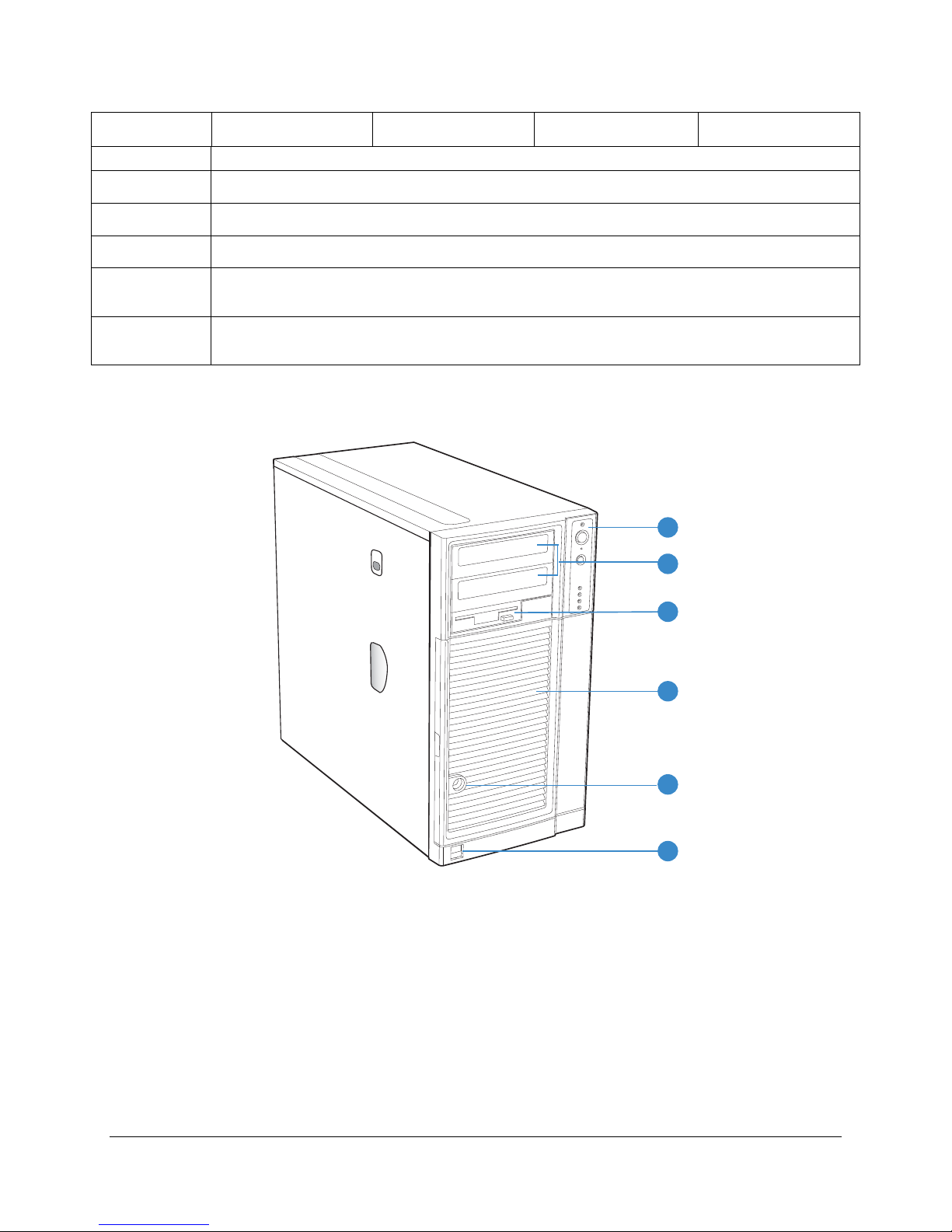
Figure 1. Front Closed Chassis View of Intel® Entry Server Chassis SC5299-E
Revision 3.1
TP01717
A. Control panel controls and indicators
B. Two half-height 5.25-in peripheral drive bays
C. 3.5-in removable media drive bay
D. Internal hard drive bay cage (behind door)
E. Security lock
F. USB ports
Intel order number D37594-005
E
F
3
Page 19
Product Overview Intel® Entry Server Chassis SC5299-E TPS
A
B
E
C
F
G
H
D
I
J
TP00866
A. Power supply (fixed power supply shown)
B. AC input power connector
C. I/O Ports
D. Expansion slot covers
E. Alternate external SCSI knockout
F. 120-mm system fan
G. Serial B port knockout
H. Location to install padlock loop
I. External SCSI knockout
J. Alternate Serial B port knockout
Figure 2. Rear Closed Chassis View of Intel® Entry Server Chassis SC5299-E
Revision 3.1
4
Intel order number D37594-005
Page 20
Intel® Entry Server Chassis SC5299-E TPS Product Overview
AF000447
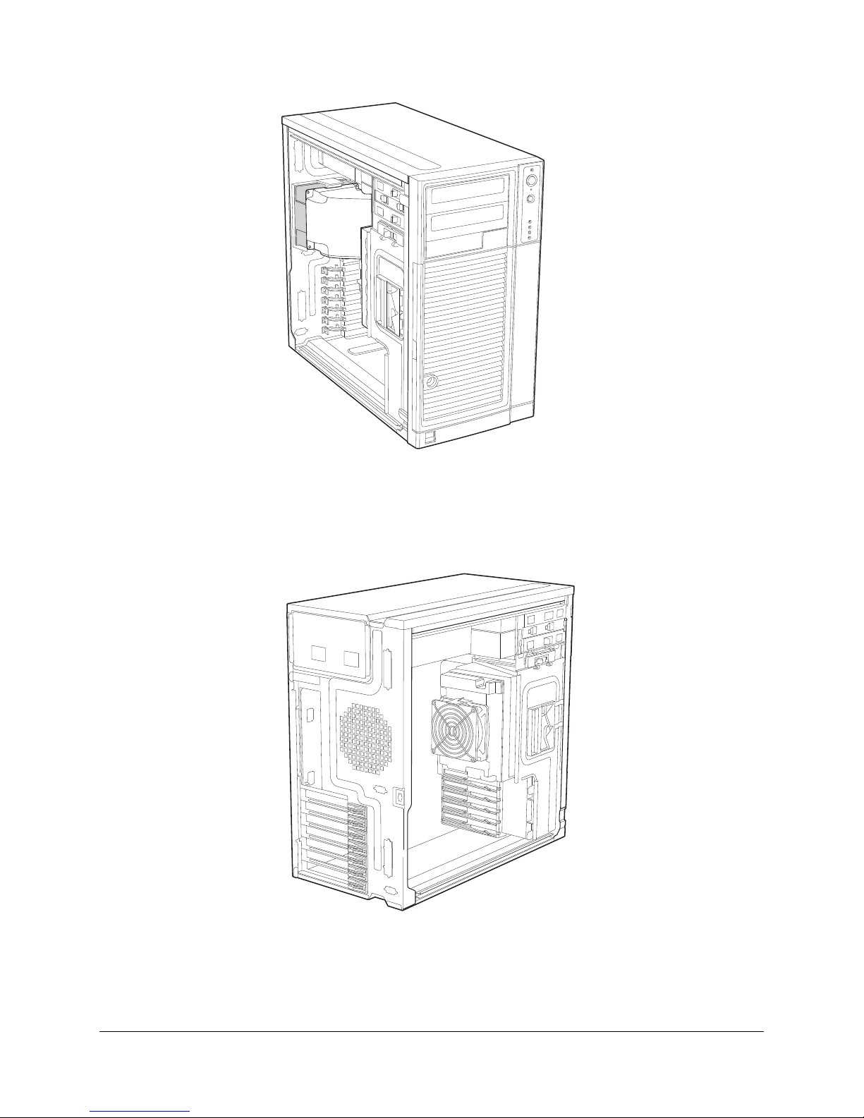
Figure 3. Front Internal Chassis View of Intel
configuration shown)
®
Entry Server Chassis SC5299-E(DP/WS/BRP
Figure 4. Rear Internal Chassis View of Intel
Revision 3.1
®
Entry Server Chassis SC5299-E with Optional Hot-
swap Drive Bay
Intel order number D37594-005
TP00868
5
Page 21
Product Overview Intel® Entry Server Chassis SC5299-E TPS
1.3 System Color
The Intel® Entry Server Chassis SC5299-E is offered in one color - Black (GE701)
1.4 Chassis Security
A variety of chassis security options are provided at the system level:
A removable padlock loop at the rear of the system access cover can be used to prevent
access to the microprocessors, memory, and add-in cards. A variety of lock sizes can be
accommodated by the 0.270-inch diameter loop.
A two-position key lock/switch will unlock the front bezel for DP, WS, and BRP
configurations.
A chassis intrusion switch is provided, allowing server management software to detect
unauthorized access to the system side cover.
Note: See the technical product specification appropriate to the server board for a description of
BIOS and management security features for each specific supported platform. Technical
product specifications can be found at http://intel.com/support
.
1.5 I/O Panel
All input/output (I/O) connectors are accessible from the rear of the chassis. The SSI E-bay
3.61-compliant chassis provides an ATX 2.2-compatible cutout for I/O shield installation. Boxed
®
Intel
server boards provide the required I/O shield for installation in the cutout. The I/O cutout
dimensions are shown in the following figure for reference.
1.750 ± 0.008
(0.150)
R 0.039 MAX, TYP
I/O Aperture
Figure 5. ATX 2.2 I/O Aperture
0.100 Min keepout around opening
Baseboard
5.196 ± 0.0106.250 ± 0.008
Datum 0,0
(0.650)
1.6 Rack and Cabinet Mounting Option
The Intel® Entry Server Chassis SC5299-E supports a rack mount configuration. The rack
mount kit includes the chassis slide rails, rack handle, rack orientation label, screws, and
manual. This rack mount kit is designed to meet the EIA-310-D enclosure specification. General
rack compatibility is further described in the Server Rack Cabinet Compatibility Guide found at
http://intel.com/support
.
Revision 3.1
6
Intel order number D37594-005
Page 22

Intel® Entry Server Chassis SC5299-E TPS Product Overview
1.7 Front Bezel Features
The bezel is constructed of molded plastic and attaches to the front of the chassis with three
clips on the right side and two snaps on the left. The snaps at the left attach behind the access
cover, thereby preventing accidental removal of the bezel. The bezel can only be removed by
first removing the server access cover. This provides additional security to the hard drive and
peripheral bay area. The bezel also includes a key-locking door that covers the drive cage area
and allows access to hot swap drives when a hot swap drive bay is installed.
The peripheral bays are covered with plastic snap-in cosmetic pieces that must be removed to
add peripherals to the system. Control panel buttons and lights are located along the right side
of the peripheral bays.
1.8 Peripheral Bays
Two 5.25-in, half-height drive bays are available for CD/DVD-ROM or tape drives as well as one
3.5-inch removable media drive bay. Drive installation is tool-less and requires no screws.
Revision 3.1
7
Intel order number D37594-005
Page 23

Power Sub-system Intel® Entry Server Chassis SC5299-E TPS
2. Power Sub-system
2.1 420-Watt Power Supply
The 420-W power supply specification defines a non-redundant power supply that supports DP
®
Intel
Xeon™ entry server systems. The 420-W power supply has 6 outputs: 3.3V, 5V, 12V1,
12V2, -12V and 5VSB. The form factor fits into a pedestal system and provides a wire harness
output to the system. An IEC connector is provided on the external face for AC input to the
power supply.
The power supply incorporates a Power Factor Correction circuit. The power supply is tested as
described in EN 61000-3-2: Electromagnetic Compatibility (EMC) Part 3: Limits- Section 2:
Limits for harmonic current emissions and meets the harmonic current emissions limits specified
for ITE equipment.
The power supply is tested as described in JEIDA MITI Guideline for Suppression of High
Harmonics in Appliances and General-Use Equipment and meets the harmonic current
emissions limits specified for ITE equipment.
Revision 3.1
8
Intel order number D37594-005
Page 24
Intel® Entry Server Chassis SC5299-E TPS Power Sub-system
2.1.1 Mechanical Overview
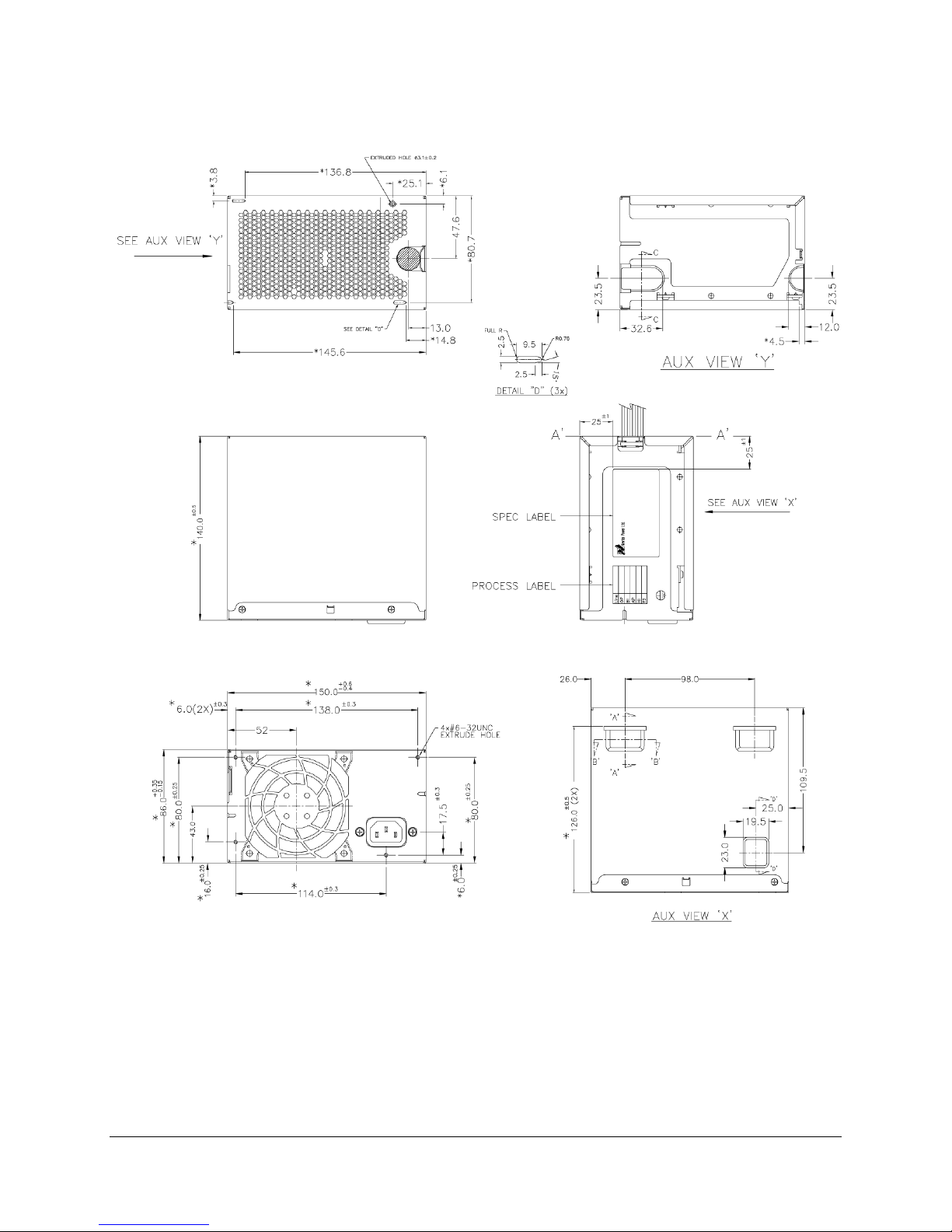
Figure 6. Mechanical Drawing for Power Supply Enclosure
Revision 3.1
9
Intel order number D37594-005
Page 25
Power Sub-system Intel® Entry Server Chassis SC5299-E TPS
2.1.2 Airflow and Temperature
The power supply operates within all specified limits over the Top temperature range. The
average air temperature difference ( T
not exceed 20C. All airflow passes through the power supply and not over the exterior surfaces
of the power supply.
Table 2. Environmental Requirements
Item Description Min Specification Units
) from the inlet to the outlet of the power supply does
ps
Top Operating temperature range. 0 50
T
Non-operating temperature range. -40 70
non-op
Altitude Maximum operating altitude 1500 m
C
C
The power supply meets UL enclosure requirements for temperature rise limits. All sides of the
power supply, with the exception of the air exhaust side, are classified as “Handle, knobs, grips,
etc. held for short periods of time only”.
2.1.3 Output Cable Harness
Listed or recognized component appliance wiring material (AVLV2), CN, rated min 105 C,
300Vdc is used for all output wiring.
Revision 3.1
10
Intel order number D37594-005
Page 26
Intel® Entry Server Chassis SC5299-E TPS Power Sub-system
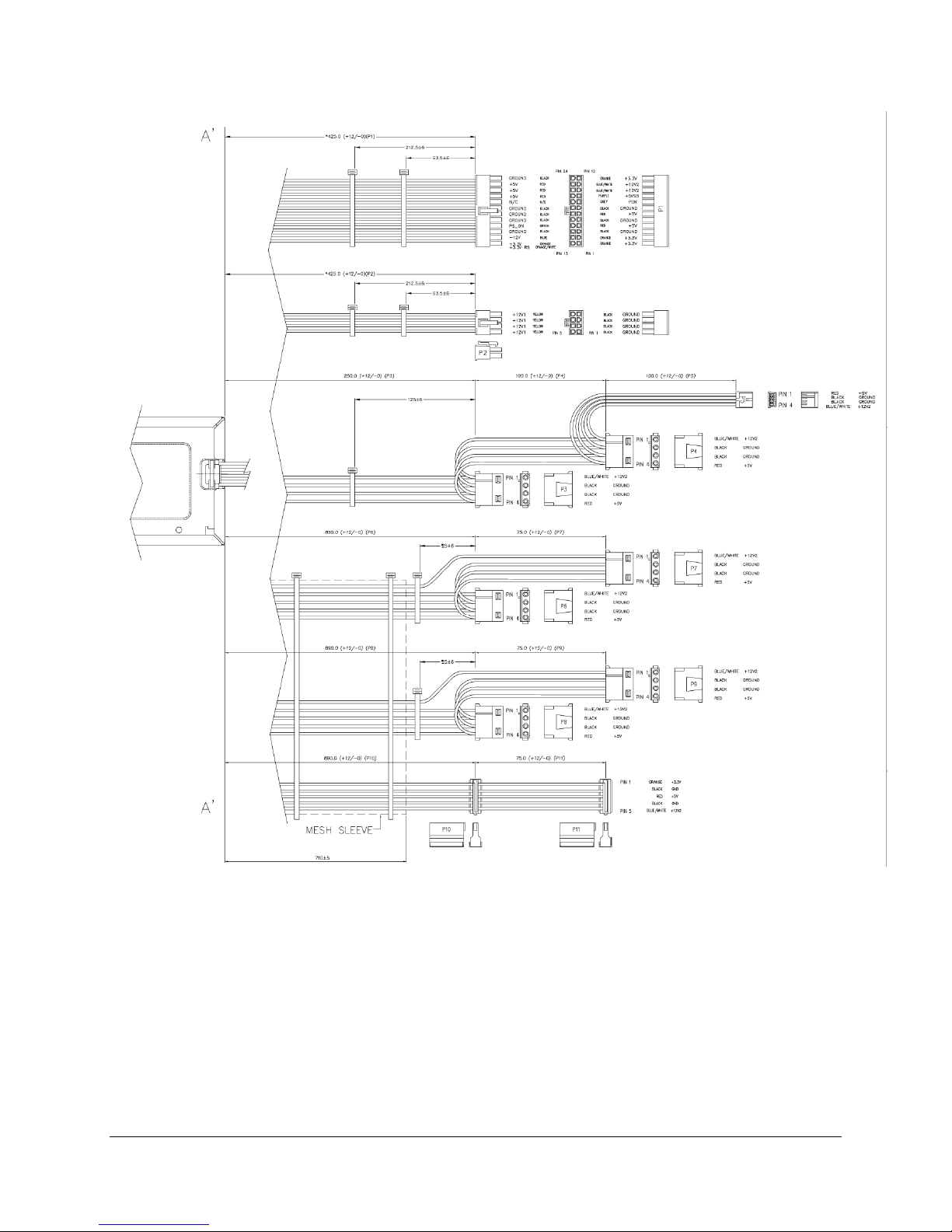
Figure 7. Output Cable Harness for 420-W Power Supply
NOTES:
1. ALL DIMENSIONS ARE IN MM
2. ALL TOLERANCES ARE +10 MM/-0 MM
3. INSTALL 1 TIE WRAP WITHIN 12MM OF THE PSU CAGE
4. MARK REFERENCE DESIGNATOR ON EACH CONNECTOR
5. TIE WRAP EACH HARNESS AT APPROX. MID POINT
6. TIE WRAP P1 WITH 2 TIES AT APPROXIMATELY 15M SPACING.
Revision 3.1
11
Intel order number D37594-005
Page 27
Power Sub-system Intel® Entry Server Chassis SC5299-E TPS
Table 3. Cable Lengths
890
Length
(mm)
No. of pins Description
5
Right-angle SATA Power
Connector
From
Power Supply cover exit hole P1 425 24 Baseboard Power Connector
Power Supply cover exit hole P2 425 8 Processor Power Connector
Power Supply cover exit hole P3 250 4 Peripheral Power Connector
Extension P4 100 4 Peripheral Power Connector
Extension from P4 P5 100 4 Floppy Power Connector
Power Supply cover exit hole P6 890 4 Peripheral Power Connector
Extension P7 75 4 Peripheral Power Connector
Power Supply cover exit hole P8 890 4 Peripheral Power Connector
Extension P9 75 4 Peripheral Power Connector
Power Supply cover exit hole P10
Extension P11 75 5 SATA Power Connector
To connector
#
2.1.3.1 P1 Baseboard Power Connector
Connector housing: 24- Pin Molex* Mini-Fit Jr.
39-01-2245 or equivalent
Contact: Molex* Mini-Fit, HCS, Female, Crimp 44476 or equivalent
Table 4. P1 Baseboard Power Connector
Pin Signal 18 AWG Color Pin Signal 18 AWG Color
1 +3.3 VDC Orange 13 +3.3 VDC* Orange
2 +3.3 VDC Orange 14 -12 VDC Blue
3 COM Black 15 COM Black
4 +5 VDC Red 16 PSON# Green
5 COM Black 17 COM Black
6 +5 VDC Red 18 COM Black
7 COM Black 19 COM Black
8 PWR OK Gray 20 Reserved N.C.
9 5VSB Purple 21 +5 VDC Red
Revision 3.1
12
Intel order number D37594-005
Page 28
Intel® Entry Server Chassis SC5299-E TPS Power Sub-system
Pin Signal 18 AWG Color Pin Signal 18 AWG Color
10 +12V2 W hite/Blue Stripe 22 +5 VDC Red
11 +12V2 W hite/Blue Stripe 23 +5 VDC Red
12 +3.3 VDC Orange 24 COM Black
Note:
3.3V Locate Sense Double Crimped into pin 13 (with #22 AWG Orange/White stripe wire).
2.1.3.2 P2 Processor Power Connector
Connector housing: 8- Pin Molex 39-01-2085 or equivalent
Contact: Molex
44476-1111 or equivalent
Table 5. P2 Processor Power Connector
Pin Signal 18 AWG Color Pin Signal 18 AWG Color
1 COM Black 5 +12V1 Yellow
2 COM Black 6 +12V1 Yellow
3 COM Black 7 +12V1 Yellow
4 COM Black 8 +12V1 Yellow
2.1.3.3 P3-P9 Peripheral Connectors
Connector housing: AMP* V0 P/N is 770827-1 or equivalent
Contact: AMP* 61314-1 contact or equivalent
Table 6. P3-P6, P8-P9 Peripheral Connectors
Pin Signal 18 AWG Color
1 +12 V2 Blue/White
2 COM Black
3 COM Black
4 +5 VDC Red
2.1.3.4 P10 Right-angle, P11 SATA Power Connectors
Connector Housing:
Contact:
Revision 3.1
13
Intel order number D37594-005
Page 29
Power Sub-system Intel® Entry Server Chassis SC5299-E TPS
Table 7. P10 Right-angle SATA Power Connector
Pin Signal 24 AWG Color
1 +3.3V Orange
2 Ground Black
3 +5V Red
4 Ground Black
5 +12V2 Blue/White
2.1.4 AC Input Requirements
The power supply operates within all specified limits over the following input voltage range,
shown in the following table. Harmonic distortion of up to 10% THD must not cause the power
supply to go out of specified limits. The power supply does power off if the AC input is less than
75VAC +/-5VAC range. The power supply starts up if the AC input is greater than 85VAC +/4VAC. Application of an input voltage below 85VAC does not cause damage to the power
supply, including a fuse blow.
Table 8. AC Input Rating
PARAMETER MIN Rated MAX Max Input
Current
Voltage (110) 90 V
Voltage (220) 180 V
Frequency 47 Hz 63 Hz
100-127 V
rms
200-240 V
rms
135 V
rms
265 V
rms
7.7 A
rms
4.3 A
rms
85Vac +/-
rms
rms
Start up VAC Power Off VAC
75Vac +/-
4Vac
5Vac
2.1.4.1 AC Inlet Connector
The AC input connector is an IEC 320 C-14 power inlet. This inlet is rated for 15A/250VAC.
2.1.4.2 Efficiency
The power supply has an efficiency of 68.5% at maximum load and over the specified AC
voltage.
2.1.4.3 AC Line Dropout/Holdup
An AC line dropout is defined to be when the AC input drops to 0VAC at any phase of the AC
line for any length of time. During an AC dropout of one cycle or less the power supply meets
dynamic voltage regulation requirements over the rated load. An AC line dropout of one cycle or
Revision 3.1
14
Intel order number D37594-005
Page 30

Intel® Entry Server Chassis SC5299-E TPS Power Sub-system
less (20ms min) does not cause any tripping of control signals or protection circuits (= 20ms
holdup time requirement). If the AC dropout lasts longer than one cycle, the power will recover
and meet all turn on requirements. The power supply meets the AC dropout requirement over
rated AC voltages, frequencies, and output loading conditions. Any dropout of the AC line does
not cause damage to the power supply.
2.1.4.3.1 AC Line 5VSB Holdup
The 5VSB output voltage stays in regulation under its full load (static or dynamic) during an AC
dropout of 70ms min (=5VSB holdup time) whether the power supply is in the ON or OFF state
(PSON asserted or de-asserted).
2.1.4.4 AC Line Fuse
The power supply has a single line fuse on the Line (Hot) wire of the AC input. The line fusing is
acceptable for all safety agency requirements. The input fuse is a slow blow type. AC inrush
current does not cause the AC line fuse to blow under any conditions. All protection circuits in
the power supply do not cause the AC fuse to blow unless a component in the power supply has
failed. This includes DC output load short conditions.
2.1.4.5 AC Inrush
AC line inrush current does not exceed 65A peak for up to 10ms, after which, the input current
is no more than the specified maximum input current at 265Vac input, 25 degrees C and full
load. The peak inrush current is less than the ratings of its critical components (including input
fuse, bulk rectifiers, and surge limiting device). For 10ms to 150ms, the inrush current should be
less than 25A peak.
The power supply meets the inrush requirements for any rated AC voltage during turn on at any
phase of AC voltage, during a single cycle AC dropout condition as well as upon recovery after
AC dropout of any duration, and over the specified temperature range (T
). AC line inrush
op
current may reach up to 60A peak for up to 1 ms.
2.1.4.6 AC Line Surge
The power supply is tested with the system for immunity to AC Ringwave and AC Unidirectional
wave, both up to 2kV, per EN 55024:1998, EN 61000-4-5:1995 and ANSI C62.45: 1992.
The power supply complies with the limits defined in EN 55024: 1998 using the IEC 61000-45:1995 test standard and performance criteria B defined in Annex B of CISPR 24.
2.1.4.7 AC Line Transient Specification
AC line transient conditions are defined as “sag” and “surge” conditions. “Sag” conditions are
also commonly referred to as “brownout”: these conditions will be defined as the AC line voltage
dropping below nominal voltage conditions. “Surge” will be defined to refer to conditions when
the AC line voltage rises above nominal voltage.
The power supply meets the requirements under the following AC line sag and surge conditions.
Revision 3.1
15
Intel order number D37594-005
Page 31

Power Sub-system Intel® Entry Server Chassis SC5299-E TPS
Table 9. AC Line Sag Transient Performance
Duration Sag Operating AC Voltage Line Frequency Performance Criteria
Continuous 10% Nominal AC Voltage ranges 50/60Hz No loss of function or performance
0 to 1 AC
cycle
> 1 AC cycle >10% Nominal AC Voltage ranges 50/60Hz Loss of function acceptable, self
Duration Surge Operating AC Voltage Line Frequency Performance Criteria
Continuous 10% Nominal AC Voltages 50/60Hz No loss of function or performance
0 to ½ AC
cycle
100% Nominal AC Voltage ranges 50/60Hz No loss of function or performance
recoverable
Table 10. AC Line Surge Transient Performance
30% Mid-point of nominal AC
Voltages
50/60Hz No loss of function or performance
2.1.4.8 AC Line Fast Transient (EFT) Specification
The power supply meets the EN 61000-4-5 directive and any additional requirements in
IEC1000-4-5:1995 and the Level 3 requirements for surge-withstand capability, with the
following conditions and exception:
These input transients do not cause any out-of-regulation conditions, such as overshoot
and undershoot, nor do they cause any nuisance trips of any of the power supply
protection circuits
The power supply meets surge-withstand test conditions under maximum and minimum
DC-output load conditions.
2.1.4.9 AC Line Leakage Current
The maximum leakage current to ground for each power supply is 3.5mA when tested at
240VAC.
2.1.5 DC Output Specifications
2.1.5.1 Grounding
The ground of the pins of the power supply output connector provides the power return path.
The output connector ground pins are connected to safety ground (power supply enclosure).
2.1.5.2 Standby Output
The 5VSB output is present when an AC input greater than the power supply turn-on voltage is
applied.
Revision 3.1
16
Intel order number D37594-005
Page 32

Intel® Entry Server Chassis SC5299-E TPS Power Sub-system
2.1.5.3 Remote Sense
The power supply has remote sense return (ReturnS) to regulate out ground drops for all output
voltages; +3.3V, +5V, +12V1, +12V2, -12V, and 5VSB. The power supply uses remote sense
(3.3VS) to regulate out drops in the system for the +3.3V output. The +5V, +12V1, +12V2, –12V
and 5VSB outputs only use remote sense referenced to the ReturnS signal. The remote sense
input impedance to the power supply is greater than 200 on 3.3VS, 5VS. This is the value of
the resistor connecting the remote sense to the output voltage internal to the power supply.
Remote sense is able to regulate out a minimum of 200mV drop on the +3.3V output. The
remote sense return (ReturnS) is able to regulate out a minimum of 200mV drop in the power
ground return. The current in any remote sense line is less than 5mA to prevent voltage sensing
errors. The power supply operates within specification over the full range of voltage drops from
the power supply’s output connector to the remote sense points.
2.1.5.4 Power Module Output Power/Currents
The following table defines power and current ratings for the 420-W power supply. The
combined output power of all outputs does not exceed the rated output power. The power
supply meets both static and dynamic voltage regulation requirements for the minimum loading
conditions.
Voltage
+5V 2A 20A 4.80 - 5.25V 50mV
+3V3 0.5A 17A 3.135 - 3.47V 50mV
–12V 0A 0.5A -11.52 - -12.6V 120mV
+5VSB 0A 2A 4.80 – 5.25V 70mV
+12V1 0.5A 24A 11.40 - 12.6V 120mV
+12V2 0.5A 17A 11.40 - 12.6V 120mV
Notes:
1. Noise test: noise bandwidth is from 10 Hz to 20 MHz.
2. Add 0.1 uF and 10uF low ESR capacitors at output connector terminals for ripple and noise
measurements.
3. Main O/P shall be enabled by pulled “remote” pin to TTL low level, and disabled by pulled “remote”
pin to TTL high level.
4. Max combined power on +5V and +3.3V outputs does not exceed 150 W.
5. 12V1 and 12V2 combined current does not exceed 30A.
6. 12V1 and 12V2 combined peak current does not exceed 34 A for over 12 seconds.
7. All outputs remain within regulation limits.
8. Maximum power does not exceed 450 W at 25 degrees C ambient and 420 W at 50 degrees C
ambient.
Table 11. Load Ratings
Load Range Output
Min. Max.
Regulation Ripple and Noise
Max. mV P-P
Revision 3.1
17
Intel order number D37594-005
Page 33

Power Sub-system Intel® Entry Server Chassis SC5299-E TPS
2.1.5.5 Voltage Regulation
The power supply output voltages are within the following voltage limits when operating at
steady state and dynamic loading conditions. These limits include the peak-peak ripple/noise.
All outputs are measured with reference to the return remote sense signal (ReturnS). The 5V,
12V1, 12V2, –12V and 5VSB outputs are measured at the power supply connectors referenced
to ReturnS. The +3.3V is measured at the remote sense signal (3.3VS) located at the signal
connector.
Table 12. Voltage Regulation Limits
Parameter Tolerance MIN NOM MAX Units
+ 3.3V - 5%/+5% +3.135 +3.30 +3.47 V
+ 5V - 4%/+5% +4.80 +5.00 +5.25 V
+ 12V1 - 5%/+ 5% +11.40 +12.00 +12.60 V
+ 12V2 - 5%/+ 5% +11.40 +12.00 +12.60 V
- 12V - 5%/+4% -11.52 -12.00 -12.60 V
+ 5VSB - 4%/+5% +4.80 +5.00 +5.25 V
rms
rms
rms
rms
rms
rms
2.1.5.6 Dynamic Loading
The output voltages are within limits specified for the step loading and capacitive loading
specified in the following table. The step load may occur anywhere within the MIN load to the
MAX load conditions.
Table 13. Transient Load Requirements
Parameter Output Range MAX Step Voltage Overshoot/Undershoot
+12V1DC 0.5A TO 18A 6A
350mV (700mVpk-pk)
+12V2DC 0.5A TO 15A 6A
+5VDC 2A TO 20A 5A
+3.3VDC 0.5A TO 17A 6A
+5VSB 0.1A TO 2.0A 0.7A
Revision 3.1
18
350mV (700mVpk-pk)
200mV(400mVpk-pk)
200mV (400mVpk-pk)
250mV(500mVpk-pk)
Intel order number D37594-005
Page 34

Intel® Entry Server Chassis SC5299-E TPS Power Sub-system
2.1.5.7 Capacitive Loading
The power supply is stable and meets all requirements with the following capacitive loading
ranges.
Table 14. Capacitive Loading Conditions
Output MIN MAX Units
+3.3V 250 6,800
+5V 400 4,700
+12V(1, 2) 500 each 11,000
-12V 1 350
+5VSB 20 350
F
F
F
F
F
2.1.5.8 Closed Loop Stability
The power supply is unconditionally stable under all line/load/transient load conditions, including
capacitive load ranges. A minimum of: 45 degrees phase margin and -8dB-gain margin is
required. Closed-loop stability is ensured at the maximum and minimum loads as applicable.
2.1.5.9 Ripple/Noise
The maximum allowed ripple/noise output of the power supply is defined in the following table.
This is measured over a bandwidth of 0 Hz to 20 MHz at the power supply output connectors.
Table 15. Ripple and Noise
+3.3V +5V +12V1/2 -12V +5VSB
50mVp-p 50mVp-p 120mVp-p 120mVp-p 50mVp-p
2.1.5.10 Timing Requirements
The timing requirements for power supply operation are as follows. The output voltages must
rise from 10% to within regulation limits (T
allowed to rise from 1.0 to 70ms. The +3.3V, +5V and +12V output voltages should start to rise
approximately at the same time. All outputs must rise monotonically. The +5V output needs to
be greater than the +3.3V output during any point of the voltage rise. The +5V output must
never be greater than the +3.3V output by more than 2.25V. Each output voltage shall reach
regulation within 50ms (T
vout_on
voltage shall fall out of regulation within 400msec (T
following figure shows the timing requirements for the power supply being turned on and off via
the AC input, with PSON held low and the PSON signal, with the AC input applied.
Revision 3.1
) within 2 to 20ms, except for 5VSB which is
vout_rise
) of each other during turn on of the power supply. Each output
) of each other during turn off. The
vout_off
Intel order number D37594-005
19
Page 35

Power Sub-system Intel® Entry Server Chassis SC5299-E TPS
Table 16. Output Voltage Timing
Item Description Minimum Maximum Units
T
Output voltage rise time from each main output. 2.0 20 msec
vout_rise
T
All main outputs must be within regulation of each
vout_on
T
All main outputs must leave regulation within this
vout_off
other within this time.
time.
50 msec
400 msec
Vout
V1
10%
Vout
V2
V3
T
vout rise
T
vout_on
T
vout_off
Item Description Minimum Maximum Units
T
sb_on_delay
T
ac_on_delay
T
vout_holdup
Revision 3.1
20
Delay from AC being applied to 5VSB being within
regulation.
Delay from AC being applied to all output voltages being
within regulation.
Time all output voltages stay within regulation after loss of
AC.
Figure 8. Output Voltage Timing
Table 17. Turn On/Off Timing
Intel order number D37594-005
1000
2500
21
msec
msec
msec
Page 36

Intel® Entry Server Chassis SC5299-E TPS Power Sub-system
Item Description Minimum Maximum Units
T
pwok_holdup
T
pson_on_delay
T
pson_pwok
T
pwok_on
T
pwok_off
T
pwok_low
T
sb_vout
T
5VSB_holdup
Delay from loss of AC to de-assertion of PWOK. 20 msec
Delay from PSON# active to output voltages within regulation
limits.
Delay from PSON# deactive to PWOK being de-asserted. 50 msec
Delay from output voltages within regulation limits to PWOK
asserted at turn on.
Delay from PWOK de-asserted to output voltages (3.3V, 5V,
12V, -12V) dropping out of regulation limits.
Duration of PWOK being in the de-asserted state during an
off/on cycle using AC or the PSON signal.
Delay from 5VSB being in regulation to O/Ps being in
regulation at AC turn on.
Time the 5VSB output voltage stays within regulation after
loss of AC.
5 400
100 1000
1
100
50 1000
70
msec
msec
msec
msec
msec
msec
2.1.5.11 Residual Voltage Immunity in Standby Mode
The power supply is immune to any residual voltage placed on its outputs (typically a leakage
voltage through the system from standby output) up to 500mV. There is neither additional heat
generated, nor stress of any internal components with this voltage applied to any individual
output, and all outputs simultaneously. It also does not trip the protection circuits during turn on.
The residual voltage at the power supply outputs for no load condition does not exceed 100mV
when AC voltage is applied.
2.1.6 Protection Circuits
Protection circuits inside the power supply cause only the power supply’s main outputs to
shutdown. If the power supply latches off due to a protection circuit tripping, an AC cycle OFF
for 15 sec and a PSON# cycle HIGH for 1sec will reset the power supply.
2.1.6.1 Over-Current Protection (OCP)
The power supply has a current limit to prevent the +3.3V, +5V, and +12V outputs from
exceeding 240VA. If the current limits are exceeded, the power supply will shut down and latch
off. The latch will be cleared by toggling the PSON
power supply will not be damaged from repeated power cycling in this condition. -12V and 5VSB
are protected under over current or shorted conditions so that no damage can occur to the
power supply. An auto-recovery feature exists on the 5VSB rail.
2.1.6.2 Over Voltage Protection (OVP)
The power supply over voltage protection is locally sensed. The power supply will shut down
and latch off after an over voltage condition occurs. This latch can be cleared by toggling the
PSON
#
signal or by an AC power interruption. The following table contains the over voltage
#
signal or by an AC power interruption. The
Revision 3.1
21
Intel order number D37594-005
Page 37

Power Sub-system Intel® Entry Server Chassis SC5299-E TPS
limits. The values are measured at the output of the power supply’s connectors. The voltage
never exceeds the maximum levels when measured at the power pins of the power supply
connector during any single point of fail. The voltage will not trip any lower than the minimum
levels when measured at the power pins of the power supply connector.
Exception: +5VSB rail will recover after its over voltage condition occurs.
Table 18. Over Voltage Protection Limits
Output Voltage MIN (V) MAX (V)
+3.3V 3.71 4.2
+5V 5.62 6.5
+12V1,2 13.4 15.0
-12V -13.5 -15.0
+5VSB 5.7 6.5
2.1.6.3 Over Temperature Protection (OTP)
The power supply is protected against over temperature conditions caused by loss of fan
cooling or excessive ambient temperature. In an OTP condition the PSU will shut down. When
the power supply temperature drops to within specified limits, the power supply will restore
power automatically, while the 5VSB always remains on. The OTP circuit has a built-in
hysteresis such that the power supply will not oscillate on and off due to a temperature
recovering condition. The OTP trip level has a minimum of 4 C of ambient temperature
hysteresis.
2.1.6.4 PSON# Input Signal
The PSON
#
signal is required to remotely turn on/off the power supply. PSON# is an active low
signal that turns on the +3.3V, +5V, +12V, and -12V power rails. When this signal is not pulled
low by the system, or left open, the outputs (except the +5VSB) turn off. This signal is pulled to
a standby voltage by a pull-up resistor internal to the power supply.
Revision 3.1
22
Intel order number D37594-005
Page 38

Intel® Entry Server Chassis SC5299-E TPS Power Sub-system
Table 19. PSON# Signal Characteristic
Signal Type
PSON# = Low ON
PSON# = High or Open OFF
Logic level low (power supply ON) 0V 1.0V
Logic level high (power supply OFF) 2.0V 5.25V
Source current, Vpson = low 4mA
Power up delay: T
PWOK delay: T
pson_on_delay
pson_pwok
5msec 400msec
50msec
Accepts an open collector/drain input from the system.
Pull-up to 5V located in power supply.
MIN MAX
2.1.6.5 PWOK (Power OK) Output Signal
PWOK is a power OK signal and is pulled HIGH by the power supply to indicate that all the
outputs are within the regulation limits of the power supply. When any output voltage falls below
regulation limits or when AC power has been removed for a time sufficiently long that the power
supply operation is no longer guaranteed, PWOK will be de-asserted to a LOW state. The start
of the PWOK delay time is inhibited as long as any power supply output is within current limit.
Table 20. PWOK Signal Characteristics
Signal Type
PWOK = High Power OK
PWOK = Low Power Not OK
Logic level low voltage, Isink=4mA 0V 0.4V
Logic level high voltage, Isource=200 A
Sink current, PWOK = low 4mA
Source current, PWOK = high 2mA
PWOK delay: T
PWOK rise and fall time
Power down delay: T
100ms 1000ms
pwok_on
1ms 200msec
pwok_off
Revision 3.1
Open collector/drain output from power supply. Pull-up
to VSB located in system.
MIN MAX
2.4V 5.25V
100 sec
23
Intel order number D37594-005
Page 39

Power Sub-system Intel® Entry Server Chassis SC5299-E TPS
2.2 550-Watt Power Supply
The 550-W power supply specification defines a non-redundant power supply that supports
dual-processor Intel
®
Xeon® entry server systems. The 550-W power supply has 6 outputs:
3.3V, 5V, 12V1, 12V2, -12V and 5VSB. The form factor is SSI EPS12V at 140mm or 180mm
depth.
Mechanical form factor: 86-mm x 150-mm x (140-mm or 180-mm) (H x W x D)
Wire harness output
Cooling: Single 80-mm or 120-mm fan
Variable fan speed based on output load and ambient temperature
Output Loading: 550W: 3.3V/24A, 5V/24A, 12Vtotal/40A, 12V1/40A, 12V2/16A,
-12V/0.5A, 5VSB/3A
550W @ 45 degrees C (added 12V power)
Efficiency recommendation: ~ 70% efficiency @ 100% load, 90VAC
Acoustics: 6.5 BA @ 100% load, 45 degrees C
5.2 BA @ 60% load, 40 degrees C
4.7 BA @ 40% load, 35 degrees C
AC Input: 90VAC to 264AV
Power Factor Corrected to meet EN61000-3-2
Holdup time: 12 msec @ 100% load
20 msec @ 75% load
SMBus (PSMI): No PSMI features
Protection: over current, over temperature, over voltage
240VA protection on 3.3V, 5V, 12V2, -12V, and 5VSB (no 240VA
protection on 12V1)
LED: No LEDs
Environmental: 45 degrees C max inlet temperature
5,000 feet altitude
EMI: EN55022/CISPR 22 – Class A (10dB margin) @ 75% load
Reliability: 100,000 hours MTBF and 3 year life @ 75% load, 40 degrees C,
100VAC
Standard Intel component de-ratings
Ecology: RoHS compliant per directive 2002/95/EC (lead free solder)
Revision 3.1
24
Intel order number D37594-005
Page 40

Intel® Entry Server Chassis SC5299-E TPS Power Sub-system
2.2.1 Mechanical Outline
12 mm
55 mm
130 mm
11 mm
110 mm
97.2 mm
Airflow
146 mm
15 mm
140 mm
Label Area
16 mm
6 mm 114 mm
Up
150 mm
138 mm
Warning
Label
AC
Inlet
86 mm
6x32 THREADED HOLE
(4x)
74 mm
Figure 9. Mechanical Drawing for Power Supply Enclosure
2.2.1.1 Airflow Requirements
The power supply shall incorporate an 80-mm fan for self cooling and system cooling. The
airflow direction shall be from the wire internal face of the power supply to the external face. The
power supply shall have adequate airflow with the following system airflow restriction.
Revision 3.1
25
Intel order number D37594-005
Page 41

Power Sub-system Intel® Entry Server Chassis SC5299-E TPS
System Flow Impedance
0.6
0.5
0.4
0.3
0.2
(in H2O)
0.1
System P ressure
0
010203040
Power Supply Airflow (CFM)
Figure 10. System Airflow Impedance
2.2.1.2 Acoustic Requirements
The fans speed shall vary linearly based on output loading and ambient temperature. The
declared sound power levels (LwAd) of the power supply unit (PSU) must meet the
requirements shown in the table below. Sound power must be measured according to ECMA 74
(www.ecma-international.org) and reported according to ISO 9296.
The acoustic measurement of the PSU shall be performed with the PSU fan operating at the
RPM corresponding to the operating conditions shown in the table below. The PSU acoustic
test report shall at the minimal include the PSU dimension, picture, fan model and size, fan
voltage (or duty cycle), RPM and PSU sound power level at each operating condition. The
proper RPM thermally sustainable shall be determined through PSU thermal testing, and shall
be submitted as appendix to the acoustic test report.
Table 21. Acoustic Requirements
Operating Conditions Inlet Temperature
Condition
Maximum 45ºC 100% 6.5
Operating
Idle
40 C
35 C
% of Maximum Loading
Condition
60% 5.2
40% 4.7
LwAd (BA)
2.2.1.3 Temperature Requirements
The power supply operates within all specified limits over the T
average air temperature difference ( T
not exceed 20 degrees C. All airflow passes through the power supply and not over the exterior
surfaces of the power supply.
Revision 3.1
26
) from the inlet to the outlet of the power supply does
ps
Intel order number D37594-005
temperature range. The
op
Page 42

Intel® Entry Server Chassis SC5299-E TPS Power Sub-system
Table 22. Environmental Requirements
Item Description MIN Specification Units
Top Operating temperature range. 0 45
T
Non-operating temperature range. -40 70
non-op
Altitude Maximum operating altitude 1500 m
C
C
The power supply meets UL enclosure requirements for temperature rise limits. All sides of the
power supply, with exception of the air exhaust side, must be classified as “Handle, knobs,
grips, etc. held for short periods of time only”.
2.2.2 AC Input Voltage Requirements
The power supply operates within all specified limits over the input voltage range shown in the
following table. Harmonic distortion of up to 10% THD must not cause the power supply to go
out of specified limits. The power supply will power off if the AC input is less than 75VAC +/5VAC range. The power supply starts up if the AC input is greater than 85VAC +/-4VAC.
Application of an input voltage below 85VAC will not cause damage to the power supply,
including a fuse blow.
Table 23. AC Input Rating
Parameter MIN Rated MAX Start up VAC Power Off VAC
Voltage (110) 90 V
Voltage (220) 180 V
Frequency 47 Hz 63 Hz
100-127 V
rms
200-240 V
rms
140 V
rms
264 V
rms
85Vac +/-
rms
rms
4Vac
75Vac +/5Vac
2.2.2.1 AC Inlet Connector
The AC input connector is an IEC 320 C-14 power inlet. This inlet is rated for 15A/250VAC.
2.2.2.2 AC Line Transient Specification
AC line transient conditions are defined as “sag” and “surge” conditions. “Sag” conditions are
also commonly referred to as “brownout”; these conditions will be defined as the AC line voltage
dropping below nominal voltage conditions. “Surge” will be defined to refer to conditions when
the AC line voltage rises above nominal voltage.
The power supply meets the requirements under the following AC line sag and surge conditions.
Revision 3.1
27
Intel order number D37594-005
Page 43

Power Sub-system Intel® Entry Server Chassis SC5299-E TPS
Table 24. AC Line Sag Transient Performance
Duration Sag Operating AC Voltage Line
Frequency
Continuous 10% Nominal AC Voltage ranges 50/60Hz No loss of function or performance
0 to 1 AC cycle 100% Nominal AC Voltage ranges 50/60Hz No loss of function or performance
> 1 AC cycle >10% Nominal AC voltage ranges 50/60Hz Loss of function acceptable, self
recoverable
Performance Criteria
Table 25. AC Line Surge Transient Performance
Duration Surge Operating AC Voltage Line Frequency Performance Criteria
Continuous 10% Nominal AC Voltages 50/60Hz No loss of function or performance
0 to ½ AC
cycle
30% Mid-point of nominal AC
voltages
50/60Hz No loss of function or performance
2.2.2.3 Susceptibility Requirements
The power supply meets the following electrical immunity requirements when connected to a
cage with an external EMI filter that meets the criteria defined in the SSI document EPS Power
Supply Specification.
Table 26. Performance Criteria
Level Description
A The apparatus shall continue to operate as intended. No degradation of
performance.
B The apparatus shall continue to operate as intended. No degradationof
performance beyond spec limits.
C Temporary loss of function is allowed provided the function is self-recoverable or
can be restored by the operation of the controls.
2.2.2.3.1 Electrostatic Discharge Susceptibility
The power supply complies with the limits defined in EN 55024: 1998 using the IEC 61000-42:1995 and the level 3 test standard and performance criteria B defined in Annex B of CISPR
24.
Revision 3.1
28
Intel order number D37594-005
Page 44

Intel® Entry Server Chassis SC5299-E TPS Power Sub-system
2.2.2.3.2 Fast Transient/Burst
The power supply complies with the limits defined in EN55024: 1998 using the IEC 61000-44:1995 and the level 3 test standard and performance criteria B defined in Annex B of CISPR
24.
2.2.2.3.3 Radiated Immunity
The power supply complies with the limits defined in EN55024: 1998 using the IEC 61000-43:1995 and the level 3 test standard and performance criteria A defined in Annex B of CISPR
24.
2.2.2.3.4 Surge Immunity
The power supply is tested with the system for immunity to AC Ringwave and AC Unidirectional
wave, both up to 2kV, per EN 55024:1998, EN 61000-4-5:1995 and ANSI C62.45: 1992.
The pass criteria include: no unsafe operation is allowed under any condition; all power supply
output voltage levels must stay within proper spec levels; no change in operating state or loss of
data during and after the test profile; no component damage under any condition.
The power supply complies with the limits defined in EN55024: 1998 using the IEC 61000-45:1995 test standard and performance criteria B defined in Annex B of CISPR 24.
2.2.2.4 AC Line Fast Transient (EFT) Specification
The power supply meets the EN61000-4-5 directive and any additional requirements in
IEC1000-4-5:1995 and the Level 3 requirements for surge-withstand capability, with the
following conditions and exception:
These input transients do not cause any out-of-regulation conditions, such as overshoot
and undershoot, nor do they cause any nuisance trips of any of the power supply
protection circuits.
The surge-withstand test must not produce damage to the power supply.
The supply meets surge-withstand test conditions under maximum and minimum DC-output
load conditions.
2.2.2.5 AC Line Dropout/Holdup
An AC line dropout is defined to be when the AC input drops to 0VAC at any phase of the AC
line for any length of time. During an AC dropout, the power supply meets dynamic voltage
regulation requirements. An AC line dropout of any duration does not cause tripping of control
signals or protection circuits. If the AC dropout lasts longer than the hold up time, the power
supply will recover and meet all turn on requirements. The power supply meets the AC dropout
requirement over rated AC voltages, frequencies. A dropout of the AC line for any duration does
not cause damage to the power supply.
Revision 3.1
29
Intel order number D37594-005
Page 45

Power Sub-system Intel® Entry Server Chassis SC5299-E TPS
Table 27. AC Line Dropout/Holdup
Output Wattage Loading Holdup Time
412.5 W 75% 20 msec
550 W 100% 12 msec
2.2.2.5.1 AC Line 5VSB Holdup
The 5VSB output voltage stays in regulation under its full load (static or dynamic) during an AC
dropout of 70-ms min (=5VSB holdup time) whether the power supply is in the ON or OFF state
(PSON asserted or de-asserted).
2.2.2.6 Power Recovery
The power supply recovers automatically after an AC power failure. AC power failure is defined
to be any loss of AC power that exceeds the dropout criteria.
2.2.2.6.1 Voltage Brown Out
The power supply complies with the limits defined in EN55024: 1998 using the IEC 61000-411:1995 test standard and performance criteria C defined in Annex B of CISPR 24.
In addition, the power supply meets the following Intel Requirement:
A continuous input voltage below the nominal input range shall not damage the power supply or
cause overstress to any power supply component. The power supply must be able to return to
normal power up state after a brownout condition. Maximum input current under a continuous
brownout shall not blow the fuse. The power supply should tolerate a 3min ramp from 90VAC
voltage to 0VAC after the components have reached a steady state condition.
2.2.2.6.2 Voltage Interruptions
The power supply complies with the limits defined in EN55024: 1998 using the IEC 61000-411:1995 and the level 3 test standard and performance criteria C defined in Annex B of CISPR
24.
2.2.2.7 AC Line Inrush
AC line inrush current does not exceed 50A peak for up to one-quarter of the AC cycle, after
which, the input current should be no more than the specified maximum input current. The peak
inrush current is less than the ratings of its critical components (including input fuse, bulk
rectifiers, and surge limiting device).
The power supply must meet the inrush requirements for any rated AC voltage, during turn on at
any phase of AC voltage, during a single cycle AC dropout condition, as well as upon recovery
after AC dropout of any duration, and over the specified temperature range (T
acceptable that AC line inrush current may reach up to 70A peak for up to 1 ms
Revision 3.1
30
Intel order number D37594-005
). It is
op
Page 46

Intel® Entry Server Chassis SC5299-E TPS Power Sub-system
2.2.2.8 AC Line Isolation Requirements
The power supply meets all safety agency requirements for dielectric strength. Transformers’
isolation between primary and secondary windings complies with the 3000Vac (4242Vdc)
dielectric strength criteria. In addition, the insulation system complies with reinforced insulation
per safety standard IEC 950. Separation between the primary and secondary circuits, and
primary to ground circuits, complies with the IEC 950 spacing requirements.
2.2.2.9 AC Line Leakage Current
The maximum leakage current to ground for each power supply is 3.5mA when tested at
240VAC.
2.2.2.10 AC Line Fuse
The power supply has a single line fuse on the line (hot) wire of the AC input. The line fusing is
acceptable for all safety agency requirements. The input fuse is a slow blow type. AC inrush
current does not cause the AC line fuse to blow under any conditions. All protection circuits in
the power supply do not cause the AC fuse to blow unless a component in the power supply has
failed. This includes DC output load short conditions.
2.2.2.11 Power Factor Correction
The power supply incorporates a Power Factor Correction circuit.
The power supply is tested as described in EN 61000-3-2: Electromagnetic Compatibility (EMC)
Part 3: Limits - Section 2: Limits for harmonic current emissions, and meets the harmonic
current emissions limits specified for ITE equipment.
The power supply is tested as described in JEIDA MITI Guideline for Suppression of High
Harmonics in Appliances and General-Use Equipment and meets the harmonic current
emissions limits specified for ITE equipment.
2.2.3 Efficiency
The following table provides the required minimum efficiency level at various loading conditions.
These are provided at three different load levels: 100%, 50% and 20%. Efficiency is tested over
an AC input voltage range of 115VAC to 220VAC.
Table 28. Efficiency
Loading 100% of Maximum 50% of Maximum 20% of Maximum
Recommended Efficiency 70% 72% 65%
2.2.4 DC Output Specifications
2.2.4.1 Output Connectors
Listed or recognized component appliance wiring material (AVLV2), CN, rated minimum 105
degrees C , 300VDC is used for all output wiring.
Revision 3.1
31
Intel order number D37594-005
Page 47

Power Sub-system Intel® Entry Server Chassis SC5299-E TPS
Table 29. Cable Lengths
From Length (mm)
Power Supply cover exit hole 425 P1 24 Baseboard Power Connector
Power Supply cover exit hole 720 P2 8 Processor Power Connector
Power Supply cover exit hole 575 P12 4 +12V1 Baseboard Power Connector
Power Supply cover exit hole 250 P3 4 Peripheral Power Connector
Extension from P3 100 P4 4 Peripheral Power Connector
Extension from P4 100 P5 4 Floppy Power Connector
Power Supply cover exit hole 740 P6 4 Peripheral Power Connector
Extension from P8 75 P7 4 Peripheral Power Connector
Power Supply cover exit hole 740 P8 4 Peripheral Power Connector
Extension from P10 75 P9 4 Peripheral Power Connector
Power Supply cover exit hole 740 P10 5 Right-angle SATA Power Connector
Extension from P12 75 P11 5 SATA Power Connector
To
Connector #
Number of
Pins
Description
2.2.4.2 P1 Main Power Connector
Connector housing: 24-Pin Molex* Mini-Fit Jr.
39-01-2245 or equivalent
Contact: Molex Mini-Fit, HCS, Female, Crimp 44476 or equivalent
Table 30. P1 Main Power Connector
Pin Signal 18 AWG Color Pin Signal 18 AWG Color
1 +3.3 VDC Orange 13 +3.3 VDC* Orange
3.3RS Orange/White(24AWG) 14 -12 VDC Blue
2 +3.3 VDC Orange 15 COM Black
3 COM Black 16 PSON# Green (24AWG)
4 +5 VDC Red 17 COM Black
5 COM Black COMRS Black (24AWG)
6 +5 VDC Red 18 COM Black
7 COM Black 19 COM Black
8 PWR OK Gray 20 Reserved N.C.
9 5VSB Purple 21 +5 VDC Red
10 +12V2 Yellow 22 +5 VDC Red
11 +12V2 Yellow 23 +5 VDC Red
12VRS Yellow/White (24AWG) 5VRS Red/White (24AWG)
Revision 3.1
32
Intel order number D37594-005
Page 48

Intel® Entry Server Chassis SC5299-E TPS Power Sub-system
Pin Signal 18 AWG Color Pin Signal 18 AWG Color
12 +3.3 VDC Orange 24 COM Black
Note: 5V Remote sense may be double crimped into pin 4 if required to meet voltage regulation at the output connectors.
2.2.4.3 P2 Processor Power Connector
Connector housing: 8-Pin Molex* 39-01-2085 or equivalent
Contact: Molex
44476-1111 or equivalent
Table 31. P2 Processor Power Connector
Pin Signal 18 AWG Color Pin Signal 18 AWG Color
1 COM Black 5 +12V1 Yellow
2 COM Black 6 +12V1 Yellow
3 COM Black 7 +12V1 Yellow
4 COM Black 8 +12V1 Yellow
2.2.4.4 P12 Baseboard Power Connector
Connector housing: 4-Pin Molex* 39-01-2040 or equivalent
Contact: Molex
Pin Signal 18 AWG Color Pin Signal 18 AWG Color
1 COM Black 3 +12V1 Yellow
Mini-Fit Jr, HCS, 44476-1111 or equivalent
Table 32. P12 Baseboard Power Connector
2 COM Black 4 +12V1 Yellow
2.2.4.5 P3, P4, P6, P7, P8, P9 Peripheral Power Connectors
Connector housing: AMP* 1-480424-0 or equivalent
Contact: Amp 61314-1 contact or equivalent
Table 33. P3, P4, P6, P7, P8, P9 Peripheral Power Connectors
Pin Signal 18 AWG Color
1 +12 V2 Green
2 COM Black
3 COM Black
4 +5 VDC Red
Revision 3.1
Intel order number D37594-005
33
Page 49

Power Sub-system Intel® Entry Server Chassis SC5299-E TPS
2.2.4.6 P5 Floppy Power Connector
Connector housing: AMP* 171822-4 or equivalent
Contact: Amp 170204-1 contact or equivalent
Table 34. P5 Floppy Power Connector
Pin Signal 22 AWG Color
1 +5VDC Red
2 COM Black
3 COM Black
4 +12V2 Green
2.2.4.7 P10 Right-angle SATA Power Connector
Connector housing: JWT* F6002HS0-5P-18 or equivalent
Table 35. P10 SATA Power Connectors
Pin Signal 18 AWG Color
1 +3.3V Orange
2 COM Black
3 +5VDC Red
4 COM Black
5 +12V2 Green
2.2.4.8 P11 SATA Power Connector
Connector housing: JWT A3811H00-5P or equivalent
Contact: JWT A3811TOP-0D or equivalent
Table 36. P11 SATA Power Connectors
Pin Signal 18 AWG Color
1 +3.3V Orange
2 COM Black
3 +5VDC Red
Revision 3.1
34
Intel order number D37594-005
Page 50

Intel® Entry Server Chassis SC5299-E TPS Power Sub-system
Pin Signal 18 AWG Color
4 COM Black
5 +12V2 Green
2.2.4.9 Output Power/Currents
The following table defines power and current ratings for the 550-W power supply. The
combined output power of all outputs does not exceed the rated output power. The power
supply meets both static and dynamic voltage regulation requirements for the minimum loading
conditions.
Table 37. Load Ratings
Output Voltage Minimum
Continuous
+3.3V 1.0A 24A
+5V 2A 24A
+12V1 0.5A 40A 48A
+12V2 1.0A 16A 22A (500msec)
–12V 0A 0.5A
+5VSB 0.1A 3A 3.5A
Notes:
1. Maximum continuous total output power will not exceed 550 W.
2. The maximum continuous total output power capability increases at lower ambient temperatures at a rate of
3.3W/degree C up to 600 W with a 30 degrees C ambient temperature.
3. Maximum continuous load on the combined 12V output will not exceed 40A at 45 degrees C, ramping up to
44 A at 30 degrees C.
4. Peak load on the combined 12V output will not exceed 48 A.
5. Peak total DC output power will not exceed 600 W.
6. Peak power and current loading is supported for a minimum of 12 seconds
7. Combined 3.3V and 5V power should not exceed 160 W.
Maximum
Continuous
Peak
2.2.4.10 Power On Loading
The power supply operates at lighter load conditions when the system first powers on. Under
these conditions, the voltage regulation limits are relaxed. Power on loading and voltage
regulation requirements are defined in the following tables.
Time duration is 1 second during power on.
Revision 3.1
35
Intel order number D37594-005
Page 51

Power Sub-system Intel® Entry Server Chassis SC5299-E TPS
Table 38. Power On Load Ratings
Voltage Minimum Continuous Maximum Continuous Peak
+3.3 V 0 A 9 A
+5 V 0 A 7 A
+12 V1 0 A 16 A
+12 V2 0.1 A 5 A
-12 V 0 A 0.5 A
+5 VSB 0.1 A 3.0 A 3.5 A
Table 39. Power On Voltage Regulation Limits
Parameter Tolerance MIN NOM MAX Units
+ 3.3V - 10%/+10% +2.97 +3.30 +3.63 V
+ 5V - 10%/+ 10% +4.50 +5.00 +5.50 V
+ 12V1 - 8%/+10% +11.04 +12.00 +13.20 V
+ 12V2 - 8%/+10% +11.04 +12.00 +13.20 V
- 12V - 5%/+9% -11.40 -12.00 -13.08 V
+ 5VSB - 5%/+5% +4.75 +5.00 +5.25 V
rms
rms
rms
rms
rms
rms
2.2.4.11 Grounding
The ground of the pins of the power supply output connector provides the power return path.
The output connector ground pins are connected to safety ground (power supply enclosure).
This grounding is well designed to ensure passing the maximum allowed Common Mode Noise
levels.
The power supply must be provided with a reliable protective earth ground. All secondary
circuits are connected to protective earth ground. Resistance of the ground returns to chassis
does not exceed 1.0 m . This path may be used to carry DC current.
2.2.4.12 Remote Sense
The power supply has remote sense return (ReturnS) to regulate out ground drops for all output
voltages: +3.3V, +5V, +12V1, +12V2, -12V, and 5VSB. The power supply uses remote sense to
regulate out drops in the system for the +3.3V, +5V, and 12V1 outputs. The remote sense input
impedance to the power supply is greater than 200 on 3.3VS, 5VS. This is the value of the
resistor connecting the remote sense to the output voltage internal to the power supply. Remote
sense must be able to regulate out a minimum of 200mV drop on the +3.3V output. The remote
sense return (ReturnS) must be able to regulate out a minimum of 200mV drop in the power
Revision 3.1
36
Intel order number D37594-005
Page 52

Intel® Entry Server Chassis SC5299-E TPS Power Sub-system
ground return. The current in any remote sense line is less than 5 mA to prevent voltage
sensing errors. The power supply operates within specification over the full range of voltage
drops from the power supply’s output connector to the remote sense points.
2.2.4.13 Standby Output
The 5VSB output is present when an AC input greater than the power supply turn on voltage is
applied.
2.2.4.14 Voltage Regulation
The power supply output voltages are within the following voltage limits when operating at
steady state and dynamic loading conditions. These limits include the peak-peak ripple/noise.
All outputs are measured with reference to the return remote sense signal (ReturnS). The 5V,
12V1, 12V2, –12V and 5VSB outputs are measured at the power supply connectors referenced
to ReturnS. The +3.3V is measured at its remote sense signal (3.3VS) located at the signal
connector.
Table 40. Voltage Regulation Limits
Parameter Tolerance MIN NOM MAX Units
+ 3.3V - 5%/+5% +3.14 +3.30 +3.46 V
+ 5V - 5%/+5% + 4.75 +5.00 +5.25 V
+ 12V1 - 5%/+ 5% +11.40 +12.00 +12.60 V
+ 12V2 - 5%/+ 5% +11.40 +12.00 +12.60 V
- 12V - 5%/+9% -11.40 -12.00 -13.08 V
+ 5VSB - 5%/+5% +4.75 +5.00 +5.25 V
rms
rms
rms
rms
rms
rms
2.2.4.15 Dynamic Loading
The output voltages are within limits specified for the step loading and capacitive loading
specified in the following table. The load transient repetition rate is tested between 50Hz and
5kHz at duty cycles ranging from 10%-90%. The step load may occur anywhere between the
MIN load and MAX load conditions.
Table 41. Transient Load Requirements
Output Step Load Size (see
+3.3VDC 5.0A
+5V
Revision 3.1
Load Slew Rate Test Capacitive Load
note 2)
0.25 A/ sec
4.0A 0.25 A/ sec 400 F
250 F
Intel order number D37594-005
37
Page 53

Power Sub-system Intel® Entry Server Chassis SC5299-E TPS
Output Step Load Size (see
note 2)
+12V1 25.0A
+12V2 25.0A
+5VSB 0.5A
Notes:
1. Step loads on each 12V output may happen simultaneously.
2. The +12V should be tested with 2200 F evenly split between the two +12V rails.
Load Slew Rate Test Capacitive Load
0.25 A/ sec 2200 F
0.25 A/ sec 2200 F
0.25 A/ sec 20 F
1,2
1,2
2.2.4.16 Capactive Loading
The power supply is stable and meets all requirements with the following capacitive loading
ranges.
Table 42. Capacitive Loading Conditions
Output MIN MAX Units
+3.3V 250 6,800
+5V 400 4,700
F
F
+12V(1, 2) 500 each 11,000
-12V 1 350
+5VSB 20 350
F
F
F
2.2.4.17 Closed Loop Stability
The power supply is unconditionally stable under all line/load/transient load conditions, including
capacitive load ranges. A minimum of 45 degrees phase margin and -10dB-gain margin is
required. Closed-loop stability is ensured at the maximum and minimum loads as applicable.
2.2.4.18 Common Mode Noise
The common mode noise on any output shall not exceed 350mV pk-pk over the frequency band
of 10Hz to 30MHz.
2.2.4.19 Ripple/Noise
The maximum allowed ripple/noise output of the power supply is defined in the following table.
This is measured over a bandwidth of 0 Hz to 20 MHz at the power supply output connectors. A
10 F tantalum capacitor, in parallel with a 0.1 F ceramic capacitor, is placed at the point of
measurement.
Revision 3.1
38
Intel order number D37594-005
Page 54

Intel® Entry Server Chassis SC5299-E TPS Power Sub-system
Table 43. Ripple and Noise
+3.3V +5V +12V1/2 -12V +5VSB
50mVp-p 50mVp-p 120mVp-p 120mVp-p 50mVp-p
2.2.4.20 Soft Starting
The power supply contains a control circuit that provides monotonic soft start for its outputs
without overstressing the AC line or any power supply components at any specified AC line or
load conditions. There is no requirement for rise time on the 5Vstby but the turn on/off is
monotonic.
2.2.4.21 Zero Load Stability Requirements
When the power subsystem operates in a no-load condition, it does not need to meet the output
regulation specification, but it must operate without any tripping of over-voltage or other fault
circuitry. When the power subsystem is subsequently loaded, it must begin to regulate and
source current without fault.
2.2.4.22 Timing Requirements
The timing requirements for power supply operation are as follows. The output voltages must
rise from 10% to within regulation limits (T
) within 5 to 70ms, except for 5VSB - it is
vout_rise
allowed to rise from 1.0 to 25ms. The +3.3V, +5V and +12V output voltages should start to rise
approximately at the same time. All outputs must rise monotonically. The +5V output needs to
be greater than the +3.3V output during any point of the voltage rise. The +5V output must
never be greater than the +3.3V output by more than 2.25V. Each output voltage shall reach
regulation within 50ms (T
voltage shall fall out of regulation within 400msec (T
) of each other during turn on of the power supply. Each output
vout_on
) of each other during turn off. The
vout_off
following figure shows the timing requirements for the power supply being turned on and off via
the AC input, with PSON held low and the PSON signal, with the AC input applied.
Table 44. Output Voltage Timing
Item Description Minimum Maximum Units
T
Output voltage rise time from each main output. 5.0* 70* msec
vout_rise
T
All main outputs must be within regulation of each
vout_on
T
All main outputs must leave regulation within this
vout_off
other within this time.
time.
* The 5VSB output voltage rise time shall be from 1.0 ms to 25.0 ms.
50 msec
400 msec
Revision 3.1
39
Intel order number D37594-005
Page 55

Power Sub-system Intel® Entry Server Chassis SC5299-E TPS
V out
10% V out
V1
V2
V3
V4
T
T
vout_rise
T
vout_on
vout_off
TP02313
Figure 11. Output Voltage Timing
Table 45. Turn On/Off Timing
Item Description Minimum Maximum Units
T
sb_on_delay
T
ac_on_delay
T
vout_holdup
T
pwok_holdup
T
pson_on_delay
T
pson_pwok
T
pwok_on
T
pwok_off
Delay from AC being applied to 5VSB being within
regulation.
Delay from AC being applied to all output voltages being
within regulation.
Time all output voltages stay within regulation after loss of
AC.
1500
2500
21
Delay from loss of AC to de-assertion of PWOK 20 msec
Delay from PSON# active to output voltages within regulation
limits.
5 400
Delay from PSON# deactive to PWOK being de-asserted. 50 msec
Delay from output voltages within regulation limits to PWOK
asserted at turn on.
Delay from PWOK de-asserted to output voltages (3.3V, 5V,
12V, -12V) dropping out of regulation limits.
100 500
1
msec
msec
msec
msec
msec
msec
T
Duration of PWOK being in the de-asserted state during an
pwok_low
off/on cycle using AC or the PSON signal.
Revision 3.1
40
Intel order number D37594-005
100
msec
Page 56

Intel® Entry Server Chassis SC5299-E TPS Power Sub-system
Item Description Minimum Maximum Units
T
Delay from 5VSB being in regulation to O/Ps being in
sb_vout
regulation at AC turn on.
50 1000
msec
T
5VSB_holdup
AC Input
Vout
T
PWOK
5VSB
PSON
Time the 5VSB output voltage stays within regulation after
loss of AC.
T
vout_holdup
T
AC_on_delay
T
sb_on_delay
T
sb_vout
T
pwok_on
T
pwok_holdup
T
5VSB_holdup
pwok_off
T
pwok_low
T
sb_on_delay
70
T
pwok_on
T
pson_on_delay
msec
T
pwok_off
T
pson_pwok
AC turn on/off cycle
PSON turn on/off cycle
Figure 12. Turn On/Off Timing (Power Supply Signals)
2.2.4.23 Residual Voltage Immunity in Standby Mode
The power supply is immune to any residual voltage placed on its outputs (typically a leakage
voltage through the system from standby output) up to 500mV. There is neither additional heat
generated, nor stress of any internal components with this voltage applied to any individual
output, and all outputs simultaneously. It also does not trip the protection circuits during turn on.
The residual voltage at the power supply outputs for no-load condition does not exceed 100mV
when AC voltage is applied.
2.2.5 Protection Circuits
Protection circuits inside the power supply cause only the power supply’s main outputs to
shutdown. If the power supply latches off due to a protection circuit tripping, an AC cycle OFF
for 15sec and a PSON# cycle HIGH for 1 sec will reset the power supply.
Revision 3.1
Intel order number D37594-005
41
Page 57

Power Sub-system Intel® Entry Server Chassis SC5299-E TPS
2.2.5.1 Over-current Protection (OCP)
The power supply has a current limit to prevent the +3.3V, +5V, and +12V outputs from
exceeding the values shown in the following table. If the current limits are exceeded, the power
supply will shut down and latch off. The latch will be cleared by toggling the PSON
#
signal or by
an AC power interruption. The power supply will not be damaged from repeated power cycling
in this condition. -12V and 5VSB are protected under over-current or shorted conditions so that
no damage can occur to the power supply. The auto-recovery feature is a requirement on the
5VSB rail.
Table 46. Over-current Protection
Voltage Over-current Limit (lout limit)
+3.3V 110% minimum (= 26.4A) ; 150% maximum (= 36.0A)
+5V 110% min (= 26.4A); 150% max (= 36.0A)
+12V1 50A min; 60A max
+12V2 18A min; compliant with 240VA
-12V 0.625A min; 4.0A max
5VSB 6.0A max
2.2.5.2 Over-voltage Protection (OVP)
The power supply over-voltage protection is locally sensed. The power supply will shut down
and latch off after an over-voltage condition occurs. This latch can be cleared by toggling the
PSON
#
signal or by an AC power interruption. The following table contains the over-voltage
limits. The values are measured at the output of the power supply’s connectors. The voltage
never exceeds the maximum levels when measured at the power pins of the power supply
connector during any single point of fail. The voltage will not trip any lower than the minimum
levels when measured at the power pins of the power supply connector.
Exception: The +5VSB rail should be able to recover after its over voltage condition occurs.
Table 47. Over-voltage Protection Limits
Output Voltage MIN (V) MAX (V)
+3.3V 3.9 4.5
+5V 5.7 6.5
+12V1,2 13.3 14.5
-12V -13.3 -15.6
+5VSB 5.7 6.5
Revision 3.1
42
Intel order number D37594-005
Page 58

Intel® Entry Server Chassis SC5299-E TPS Power Sub-system
2.2.5.3 Over-temperature Protection (OTP)
The power supply is protected against over-temperature conditions caused by loss of fan
cooling or excessive ambient temperature. In an OTP condition the power supply unit will shut
down. When the power supply temperature drops to within specified limits, the power supply will
restore power automatically, while the 5VSB remains always on. The OTP circuit must have
built-in hysteresis such that the power supply will not oscillate on and off due to a temperature
recovering condition. The OTP trip level has a minimum of 4 C of ambient temperature
hysteresis.
2.2.6 Control and Indicator Functions
The following sections define the input and output signals from the power supply. Signals that
can be defined as low true use the following convention:
signal# = low true
2.2.6.1 PSON# Input Signal
The PSON
signal that turns on the +3.3V, +5V, +12V, and -12V power rails. When this signal is not pulled
low by the system, or left open, the outputs (except the +5VSB) turn off. This signal is pulled to
a standby voltage by a pull-up resistor internal to the power supply.
#
signal is required to remotely turn on/off the power supply. PSON# is an active low
Table 48. PSON# Signal Characteristic
Signal Type
PSON# = Low ON
PSON# = High or Open OFF
Logic level low (power supply ON) 0V 1.0V
Logic level high (power supply OFF) 2.0V 5.25V
Source current, Vpson = low 4mA
Power up delay: T
PWOK delay: T
pson_pwok
pson_on_delay
5msec 400msec
50msec
Accepts an open collector/drain input from the system.
Pull-up to 5V located in power supply.
MIN MAX
2.2.6.2 PWOK (Power OK) Output Signal
PWOK is a power OK signal and is pulled HIGH by the power supply to indicate that all the
outputs are within the regulation limits of the power supply. When any output voltage falls below
regulation limits or when AC power has been removed for a time sufficiently long so that power
supply operation is no longer guaranteed, PWOK will be de-asserted to a LOW state. The start
of the PWOK delay time is inhibited as long as any power supply output is in current limit.
Revision 3.1
43
Intel order number D37594-005
Page 59

Power Sub-system Intel® Entry Server Chassis SC5299-E TPS
Table 49. PWOK Signal Characteristics
Signal Type
Open collector/drain output from power supply. Pull-up
to VSB located in system.
PWOK = High Power OK
PWOK = Low Power Not OK
MIN MAX
Logic level low voltage, Isink=4mA 0V 0.4V
Logic level high voltage, Isource=200 A
2.4V 5.25V
Sink current, PWOK = low 4mA
Source current, PWOK = high 2mA
PWOK delay: T
PWOK rise and fall time
Power down delay: T
100ms 1000ms
pwok_on
100 sec
1ms 200msec
pwok_off
Revision 3.1
44
Intel order number D37594-005
Page 60

Intel® Entry Server Chassis SC5299-E TPS Power Sub-system
2.3 650-W Power Supply Module
The 650-W power supply module specification defines a 1+1 redundant power supply that
supports a dual-processor Intel
®
Xeon® server system. The power supply has two outputs to
power the system: 12VDC and 5VSB. A separate cage (including the power distribution board)
is designed to plug directly to the output connector of the power supply module and provide
additional power converters to produce other required voltages. An IEC connector is provided
on the external face for AC input to the power supply. The power supply contains cooling fans
and meets acoustic requirements.
2.3.1 Mechanical Overview
2.3.1.1 Handle and Retention Mechanism
The power supply has a handle to provide a place to grip the power supply for removal and
insertion. The power supply has a simple retention mechanism to retain the power supply once
it is inserted. This mechanism withstands the specified mechanical shock and vibration
requirements. The tab on the retention mechanism is green to indicate it is a hot-swap touch
point. The latch mechanism is designed in such a way as to prevent inserting the power supply
with the power cord plugged in. This aids the hot swapping procedure: on removal, the power
cord is unplugged first, then the power supply is removed; on insertion, the power supply is
inserted first and then the power cord is plugged in.
The handle protects the operator from any burn hazard.
The plastic handle is molded in the following material:
Material Color Designation
GE 2800 Green GN3058
BAYER FR2000 Green 3200
2.3.1.2 Acoustic and Fan Speed Control Requirements
Sound power levels emitted by the power supply meet the requirements shown in the following
table. Sound power is measured as described in ISO7779. Under a condition where inlet air
temperature exceeds the limit, sound power level may exceed the limit.
The power supply incorporates a variable speed fan. The fan speed varies linearly based on
output loading and ambient temperature. The declared sound power levels (LwAd) of the power
supply unit (PSU) meet the requirements shown in the following table. Sound power is
measured according to ECMA 74 (www.ecma-international.org) and reported according to ISO
9296.
The acoustic measurement of the power supply is performed with the power supply fan
operating at the RPM corresponding to the operating conditions shown in the following table:
Revision 3.1
45
Intel order number D37594-005
Page 61

Power Sub-system Intel® Entry Server Chassis SC5299-E TPS
Table 50. Acoustic Requirements
Operating Conditions Inlet Temperature
Condition
Maximum (1+0 and 1+1) 45 ºC 100% < 6.5
Operating (1+0 and 1+1)
Idle (1+0 and 1+1)
40 C
35 C
% of Maximum Loading
Condition
60% < 5.2
40% < 4.7
LwAd (BA)
2.3.1.3 Temperature Requirements
The power supply operates within all specified limits over the T
temperature range described
op
in the following table. The average air temperature difference from the inlet to the outlet of the
power supply does not exceed 20 degrees C. All airflow passes through the power supply and
not over the exterior surfaces of the power supply.
Table 51. Thermal Requirements
Item Description MIN Max Units
Top Operating temperature range 0 45
C
T
Non-operating temperature range -40 70
non-op
Altitude Maximum operating altitude 1524
(5,000)
C
m
(ft)
The power supply meets UL enclosure requirements for temperature rise limits. All sides of the
power supply, with exception of the air exhaust side, are classified as “Handle, knobs, grips,
etc., held for short periods of time only.”
2.3.1.4 LED Marking and Identification
The LED is green or amber when lit.
2.3.2 AC Input Requirements
The 650-W power supply incorporates a universal power input with active power factor
correction, which reduces line harmonics in accordance with the EN61000-3-2 and JEIDA MITI
standards.
2.3.2.1 AC Inlet Connector
The AC input connector is an IEC 320 C-14 power inlet. This inlet is rated for 10A/250VAC.
Revision 3.1
46
Intel order number D37594-005
Page 62

Intel® Entry Server Chassis SC5299-E TPS Power Sub-system
2.3.2.2 Efficiency
The power supply has a minimum efficiency of 75% at maximum load and over an 90-264VAC
line voltage range to guarantee proper power supply cooling while mounted in the system.
2.3.2.3 AC Input Voltage Specification
The power supply operates within all specified limits over the following input voltage range, as
shown in following table. Harmonic distortion of up to 10% of rated AC input voltage will not
cause the power supply to go out of specified limits. The power supply powers off at or
after/below 75VAC +/-5VAC range. The power supply starts up at or before/above 85VAC +/4VAC. Application of an input voltage below 85VAC does not cause damage to the power
supply, including a fuse blow.
Table 52. AC Input Rating
Parameter MIN Rated MAX Start up VAC Power Off VAC Max Input
Current
Max Rated
Input AC
Current
Voltage (110) 90 V
Voltage (220) 180 V
100-127 V
rms
200-240 V
rms
140 V
rms
264 V
rms
85Vac +/-
rms
4Vac
rms
75Vac +/5Vac
9.63 A
4.82 A
rms
rms
1,3
2,3
8.7 A
4.4 A
rms
rms
4
4
Frequency 47 Hz 50/60Hz 63 Hz
Notes:
1 Maximum input current at low input voltage range shall be measured at 90Vac, at max load.
2 Maximum input current at high input voltage range shall be measured at 180VAC, at max load.
3 This is not to be used for determining agency input current markings.
4 Maximum rated input current is measured at 100VAC and 200VAC.
2.3.2.4 AC Line Transient Specification
AC line transient conditions are defined as “sag” and “surge” conditions. “Sag” conditions are
also commonly referred to as “brownout,” these conditions will be defined as the AC line voltage
dropping below nominal voltage conditions. “Surge” will be defined to refer to conditions when
the AC line voltage rises above nominal voltage. The power supply meets the requirements
under the following AC line sag and surge conditions.
Table 53. AC Line Sag Transient Performance
Duration Sag Operating AC
Voltage
Continuous 10% Nominal AC
Voltage ranges
0 to 1 AC
cycle
100% Nominal AC
Voltage ranges
Revision 3.1
Line Frequency Loading Performance Criteria
50/60Hz 100% No loss of function or performance
50/60Hz 60% No loss of function or performance
47
Intel order number D37594-005
Page 63

Power Sub-system Intel® Entry Server Chassis SC5299-E TPS
Duration Sag Operating AC
Voltage
> 1 AC cycle >10% Nominal AC
Voltage ranges
Line Frequency Loading Performance Criteria
50/60Hz 100% Loss of function acceptable, self
recoverable
Table 54. AC Line Surge Transient Performance
Duration Surge Operating AC Voltage Line Frequency Performance Criteria
Continuous 10% Nominal AC Voltages 50/60Hz No loss of function or performance
0 to ½ AC
cycle
30% Mid-point of nominal AC
Voltages
50/60Hz No loss of function or performance
2.3.2.5 AC Line Fuse
The power supply has a single line fuse on the line (hot) wire of the AC input. The line fusing is
acceptable for all safety agency requirements. The input fuse is a slow blow type. AC inrush
current will not cause the AC line fuse to blow under any conditions. All protection circuits in the
power supply will not cause the AC fuse to blow unless a component in the power supply has
failed. This includes DC output load short conditions.
2.3.2.6 AC In-rush
AC line in-rush current does not exceed 55A peak for up to one-quarter of the AC cycle, after
which the input current is no more than the specified maximum input current. The peak in-rush
current is less than the ratings of its critical components (including input fuse, bulk rectifiers, and
surge limiting device).
The power supply meets the in-rush requirements for any rated AC voltage, during turn on at
any phase of AC voltage, during a single cycle AC dropout condition, as well as upon recovery
after AC dropout of any duration, and over the specified temperature range (T
).
op
2.3.2.7 Susceptibility Requirements
The power supply meets the following electrical immunity requirements when connected to a
cage with an external EMI filter that meets the criteria defined in the SSI document EPS Power
Supply Specification.
Table 55. Performance Criteria
Level Description
A T he apparatus shall continue to operate as intended. No degradation of performance.
B T he apparatus shall continue to operate as intended. No degradation of performance
beyond spec limits.
C Temporary loss of function is allowed provided the function is self-recoverable or can be
restored by the operation of the controls.
Revision 3.1
48
Intel order number D37594-005
Page 64

Intel® Entry Server Chassis SC5299-E TPS Power Sub-system
2.3.2.7.1 Electrostatic Discharge Susceptibility
The power supply complies with the limits defined in EN 55024: 1998 using the IEC 61000-4-2:1995 test
standard and performance criteria B defined in Annex B of CISPR 24.
2.3.2.7.2 Fast Transient/Burst
The power supply complies with the limits defined in EN55024: 1998 using the IEC 61000-4-4:1995 test
standard and performance criteria B defined in Annex B of CISPR 24.
2.3.2.7.3 Radiated Immunity
The power supply complies with the limits defined in EN55024: 1998 using the IEC 61000-43:1995 test standard and performance criteria A defined in Annex B of CISPR 24.
2.3.2.7.4 Surge Immunity
The power supply has been tested with the system for immunity to AC Ringwave and AC
Unidirectional wave, both up to 2kV, per EN 55024:1998, EN 61000-4-5:1995 and ANSI C62.45:
1992.
The pass criteria included: No unsafe operation allowed under any condition; all power supply
output voltage levels remain within proper spec levels; no change in operating state or loss of
data during and after the test profile; no component damage under any condition.
The power supply complies with the limits defined in EN55024: 1998 using the IEC 61000-45:1995 test standard and performance criteria B defined in Annex B of CISPR 24.
2.3.2.8 AC Line Dropout/Holdup
Below are the AC dropout requirements.
Table 56. Holdup Requirements
Loading Holdup Time
100% 12 msec
60% 20 msec
An AC line dropout is defined to be when the AC input drops to 0VAC at any phase of the AC
line for any length of time. During an AC dropout condition, the power supply meets dynamic
voltage regulation requirements. An AC line dropout of any duration will not cause tripping of
control signals or protection circuits. If the AC dropout lasts longer than the hold up time, the
power supply recovers and meets all turn on requirements. The power supply meets the AC
dropout requirement over rated AC voltages and frequencies. A dropout of the AC line for any
duration will not cause damage to the power supply.
Revision 3.1
49
Intel order number D37594-005
Page 65

Power Sub-system Intel® Entry Server Chassis SC5299-E TPS
2.3.2.8.1 AC Line 5VSB Holdup
The 5VSB output voltage stays in regulation under its full load (static or dynamic) during an AC
dropout of 70ms min (=5VSB holdup time) whether the power supply is in an ON or OFF state
(PSON asserted or de-asserted).
2.3.2.9 AC Line Fast Transient (EFT) Specification
The power supply meets the EN61000-4-5 directive and any additional requirements in
IEC1000-4-5: 1995 and the Level 3 requirements for surge-withstand capability, with the
following conditions and exceptions:
These input transients do not cause any out-of-regulation conditions, such as overshoot
and undershoot, nor do they cause any nuisance trips of any of the power supply
protection circuits.
The surge-withstand test must not produce damage to the power supply.
The supply meets surge-withstand conditions under maximum and minimum DC-output
load conditions.
2.3.2.10 Power Recovery
The power supply recovers automatically after an AC power failure. AC power failure is defined
to be any loss of AC power that exceeds the dropout criteria.
2.3.2.10.1 Voltage Brownout
The power supply complies with the limits defined in EN55024: 1998 using the IEC 61000-411:1995 test standard and performance criteria C defined in Annex B of CISPR 24.
In addition, the power supply meets the following Intel Requirement:
o A continuous input voltage below the nominal input range shall not damage the
power supply or cause overstress to any power supply component. The power
supply must be able to return to normal power up state after a brownout condition.
Maximum input current under a continuous brownout shall not blow the fuse. The
power supply should tolerate a 3min ramp from 90VAC voltage to 0VAC after the
components have reached a steady state condition.
2.3.2.10.2 Voltage Interruptions
The power supply complies with the limits defined in EN55024: 1998 using the IEC 61000-411:1995 test standard and performance criteria C defined in Annex B of CISPR 24.
2.3.2.11 AC Line Isolation Requirements
The power supply meets all safety agency requirements for dielectric strength. Transformers’
isolation between primary and secondary windings complies with the 3000Vac (4242Vdc)
dielectric strength criteria. If the working voltage between primary and secondary dictates a
higher dielectric strength test voltage, the highest test voltage is used. In addition, the insulation
system complies with reinforced insulation per safety standard IEC 950. Separation between the
Revision 3.1
50
Intel order number D37594-005
Page 66

Intel® Entry Server Chassis SC5299-E TPS Power Sub-system
primary and secondary circuits, and primary to ground circuits, complies with the IEC 950
spacing requirements.
2.3.2.12 Power Factor Correction
The power supply incorporates a power factor correction circuit.
The power supply has been tested as described in EN 61000-3-2: Electromagnetic Compatibility
(EMC) Part 3: Limits- Section 2: Limits for harmonic current emissions, and meets the harmonic
current emissions limits specified for ITE equipment.
The power supply has been tested as described in JEIDA MITI Guideline for Suppression of
High Harmonics in Appliances and General-Use Equipment and meets the harmonic current
emissions limits specified for ITE equipment.
2.3.3 DC Output Specification
2.3.3.1 Connector
The power supply provides card edge fingers, which mate to a connector located inside the
system. It is a blind-mating type of connector that connects the power supply’s output voltages
and signals. The card edge finger pin assignments are defined in the following table.
Connector Upper Side Pin No
Gold finger edge
connector: 2X24
Table 57. Edge Finger Power Supply Connector Pin-out
Pin No.
Top.
+12V 1 2 +12V
+12V 3 4 +12V
+12V 5 6 +12V
+12V 7 8 +12V
+12V 9 10 +12V
+12V 11 12 +12V
+12V 13 14 +12V
+12V 15 16 +12V
+12V 17 18 +12V
+12V Return 19 20 +12V Return
+12V Return 21 22 +12V Return
Bottom
Bottom Side
Revision 3.1
+12V Return 23 24 +12V Return
+12V Return 25 26 +12V Return
51
Intel order number D37594-005
Page 67

Power Sub-system Intel® Entry Server Chassis SC5299-E TPS
Connector Upper Side Pin No
Top.
+12V Return 27 28 +12V Return
+12V Return 29 30 +12V Return
+12V Return 31 32 +12V Return
+12V Return 33 34 +12V Return
+12V Return 35 36 +12V Return
5VSB 37 38 A0
SDA 39 40 +12V Sharing
PS_KILL 41 42 POK
PS_ON_CTL 43 44 -PS_Present
FAN_TACH 45 46 VIN_GOOD_OUT
SCL 47 48 -OVER_TEMP
Pin No.
Bottom
Bottom Side
Signals that can be defined as low true or high true use the following convention:
Signal# = low true
Reserved pins are reserved for future use.
2.3.3.2 Grounding
The ground of the pins of the power supply output connector provide the power return path. The
output connector ground pins are connected to safety ground (power supply enclosure).
A reliable protective earth ground is provided on the power supply. All secondary circuits are
connected to protective earth ground. Resistance of the ground returns to chassis do not
exceed 1.0 m . This path may be used to carry DC current.
2.3.3.3 Remote Sense
No remote sense and remote sense return signal is required on the 650-W power supply.
2.3.3.4 Output Power/Currents
The following table defines power and current ratings for the 650-W continuous (720-W pk)
power supply in a 1+0 or 1+1 redundant configuration. The combined output power of both
outputs does not exceed the rated output power. The power supply meets both static and
dynamic voltage regulation requirements for the minimum loading conditions. Also, the power
supply supplies the listed peak currents and power for a minimum of 10 seconds. Outputs are
not required to be peak loaded simultaneously.
Revision 3.1
52
Intel order number D37594-005
Page 68

Intel® Entry Server Chassis SC5299-E TPS Power Sub-system
Table 58. Power Supply Module Load Ratings
Min Max Peak
+12 V 0 A 54 A 58 A
+5 VSB 0.1 A 3.0 A 3.5 A
650-W Voltage
2.3.3.5 Standby Output
The 5VSB output is present when an AC input greater than the power supply turn-on voltage is
applied.
2.3.3.6 Voltage Regulation
The power supply output voltages stay within the following voltage limits when operating at
steady state and dynamic loading conditions. These limits include the peak-peak ripple/noise
specified in Table 61. All outputs are measured with reference to the GND. The +12V and
+5VSB outputs are measured at the power distribution board output harness connector.
Table 59. Voltage Regulation Limits
Parameter Tolerance MIN NOM MAX Units
+ 12V - 5%/+5% +11.40 +12.00 +12.60 V
+ 5VSB - 5%/+5% +4.75 +5.00 +5.25 V
rms
rms
2.3.3.7 Dynamic Loading
The output voltages remain within limits specified for the step loading and capacitive loading
presented in the following table. The load transient repetition rate has been tested between 5
Hz and 5 kHz at duty cycles ranging from 10%-90%. The load transient repetition rate is only a
test specification. The step load may occur anywhere between the MIN load and MAX load
defined in the following table.
Table 60. Transient Load Requirements
Output Max Step Load Size Max Load Slew Rate Test Capacitive Load
12V 3.0 A
+5VSB 0.5 A
Notes:
1. Step loads on each 12V output may happen simultaneously.
2. The +12V should be tested with 2200 F evenly split between the three +12V rails.
1
0.5 A/ s 2200 F
0.5 A/ s 20 F
Revision 3.1
53
Intel order number D37594-005
Page 69

Power Sub-system Intel® Entry Server Chassis SC5299-E TPS
2.3.3.8 Capacitive Loading
The power supply is stable and meets all requirements with the following capacitive loading
ranges. Minimum capacitive loading applies to static load only.
Table 61. Capacitive Loading Conditions
Output MIN MAX Units
+12V 2000 11,000
+5VSB 1 350
F
F
2.3.3.9 Closed Loop Stability
The power supply is unconditionally stable under all line/load/transient load conditions, including
capacitive load ranges. A minimum of 45 degrees phase margin and -10dB-gain margin are
met. Closed-loop stability is ensured at the maximum and minimum loads, as applicable.
2.3.3.10 Common Mode Noise
The common mode noise on any output does not exceed 350mV pk-pk over the frequency band
of 10Hz to 20MHz.
2.3.3.11 Ripple/Noise
The maximum ripple/noise output of the power supply is defined in the following table. This is
measured over a bandwidth of 0Hz to 20MHz at the power supply output connectors. A 10 F
tantalum capacitor in parallel with a 0.1 F ceramic capacitor is placed at the point of
measurement.
2.3.3.12 Forced Load Sharing
The +12V output has forced load sharing. The output shares within 10% at full load. All current
sharing functions are implemented internal to the power supply by making use of the 12LS
signal. The power distribution board connects the 12LS signal between the two power supplies.
The failure of a power supply does not affect the load sharing or output voltages of the other
supplies still operating. The supplies are able to load share with up to 2 power supplies in
parallel and operate in a hot-swap/redundant 1+1 configuration. The 5Vsb output is not required
to actively share current between power supplies (passive sharing). The 5Vsb outputs of the
power supplies are connected together in the system so that a failure or hot swap of a
redundant power supply does not cause these outputs to go out of regulation in the system.
Revision 3.1
54
Table 62. Ripple and Noise
+12V Output +5VSB Output
120mVp-p 50mVp-p
Intel order number D37594-005
Page 70

Intel® Entry Server Chassis SC5299-E TPS Power Sub-system
2.3.3.13 Timing Requirements
The timing requirements for power supply operation are as follows. The output voltages must
rise from 10% to within regulation limits (T
) within 5 to 70 ms, except for 5VSB, which is
vout_rise
allowed to rise from 1.0 to 25 ms. All outputs rise monotonically. The following figure shows the
timing requirements for the power supply being turned on and off via the AC input, with PSON
held low and the PSON signal, with the AC input applied.
Table 63. Output Voltage Timing
Item Description Minimum Maximum Units
T
Output voltage rise time from each main output. 5.0* 70* msec
vout_rise
T
All main outputs must be within regulation of each
vout_on
other within this time.
T
All main outputs must leave regulation within this
vout_off
time.
* The 5VSB output voltage rise time shall be from 1.0 ms to 25.0 ms.
50 msec
400 msec
V out
V1
V2
V3
V4
10% V out
T
vout_rise
T
vout_on
Figure 13. Output Voltage Timing
T
vout_off
TP02313
Revision 3.1
55
Intel order number D37594-005
Page 71

Power Sub-system Intel® Entry Server Chassis SC5299-E TPS
Table 64. Turn On/Off Timing
Item Description Minimum Maximum Units
T
sb_on_delay
Delay from AC being applied to 5VSB being within
regulation.
T
ac_on_delay
Delay from AC being applied to all output voltages being
within regulation.
T
vout_holdup
Time all output voltages stay within regulation after loss of
AC.
T
pwok_holdup
T
pson_on_delay
Delay from loss of AC to de-assertion of PWOK 20 ms
Delay from PSON# active to output voltages within regulation
limits.
T
pson_pwok
T
pwok_on
Delay from PSON# deactive to PWOK being de-asserted. 50 ms
Delay from output voltages within regulation limits to PWOK
asserted at turn on.
T
Delay from PWOK de-asserted to 12V output voltage
pwok_off
dropping out of regulation limits.
T
Duration of PWOK being in the de-asserted state during an
pwok_low
off/on cycle using AC or the PSON signal.
T
Delay from 5VSB being in regulation to O/Ps being in
sb_vout
regulation at AC turn on.
1500
2500
21
5 400
100 1000
1
100
50 1000
ms
ms
ms
ms
ms
ms
ms
ms
T
5VSB_holdup
Note:
Time the 5VSB output voltage stays within regulation after
loss of AC.
1 T
vout_holdup
and T
are defined under 60% loading.
pwok_holdup
70
ms
2.3.3.14 Hot Swap Requirement
Hot swapping a power supply is the process of inserting and extracting a power supply from an
operating power system. During this process the output voltages remain within the capacitive
load limits. Up to two power supplies can be on a single AC line. The power supply hot swaps
by the following method.
Extraction: The AC power disconnects from the power supply as the power supply is
extracted from the system. This can occur in standby mode or power-on mode.
Insertion: The AC power connects to the power supply as the power supply is inserted
into the system. The power supply powers on into either standby mode or power-on
Mode.
In general, a failed (off by internal latch or external control) power supply may be removed, then
replaced with a good power supply; however, hot swap will work with both operational as well as
failed power supplies. The newly inserted power supply will get turned on into standby or Power
On mode once inserted.
Revision 3.1
56
Intel order number D37594-005
Page 72

Intel® Entry Server Chassis SC5299-E TPS Power Sub-system
2.3.3.15 Residual Voltage Immunity in Standby Mode
The power supply is immune to any residual voltage placed on its 12V output (typically a
leakage voltage through the system from standby output) up to 1000 mV. This residual voltage
does not have any adverse effects on the power supply, including additional power dissipation
or over-stressing/over-heating any internal components or adversely effect the turn-on
performance (no protection circuits tripping during turn on).
While in standby mode, at no load condition, the residual voltage on 12V output does not
exceed 100 mV.
2.3.3.16 Soft Starting
The power supply contains control circuits that provide monotonic soft start of its outputs without
overstress of the AC line or any power supply components at any specified AC line or load
conditions. There is no requirement for rise time on the 5VSB but the turn on/off is monotonic.
2.3.3.17 Zero Load Stability Requirements
When the power subsystem operates in a no-load condition in a 1+0 or 1+1 configuration, it
does not need to meet the output regulation specification, but it must operate without any
tripping of over-voltage or other fault circuitry. When the power subsystem is subsequently
loaded, it must begin to regulate and source current without fault.
2.3.4 Protection Circuits
Protection circuits inside the power supply cause only the power supply’s main outputs to shut
down. If the power supply latches off due to a protection circuit tripping, an AC cycle OFF for
15sec and a PSON# cycle HIGH for 1sec will reset the power supply.
2.3.4.1 Over-current Protection (OCP)
The power supply has a current limit to prevent the +5VSB and +12V outputs from exceeding
the values shown in the following table. If the current limits are exceeded the power supply will
shut down and latch off. The latch will be cleared by toggling the PSON
power interruption. The power supply is not damaged from repeated power cycling in this
condition. 5VSB is protected under over-current or shorted conditions so that no damage can
occur to the power supply.
Table 65. Over-current Protection (OCP)
Output
Voltage
+12V 120% min (= 65.0 A min); 140% max (= 76.0 A max)
+5VSB 120% min (= 3.6 A min); 200% max (= 6.0 A max)
Over-current Protection Limits
#
signal or by an AC
Revision 3.1
57
Intel order number D37594-005
Page 73

Power Sub-system Intel® Entry Server Chassis SC5299-E TPS
2.3.4.2 Over-voltage Protection (OVP)
The power supply’s over-voltage protection is locally sensed. The power supply will shut down
and latch off after an over-voltage condition occurs. This latch can be cleared by toggling the
PSON
#
signal or by an AC power interruption. The following table contains the over-voltage
limits. The values are measured at the output of the power supply’s connectors. The voltage
never exceeds the maximum levels when measured at the power pins of the power supply
connector during any single point of fail. The voltage will never trip any lower than the minimum
levels when measured at the power pins of the power supply connector.
Table 66. Over-voltage Protection Limits
Output Voltage MIN (V) MAX (V)
+12V 13.3 14.5
+5VSB 5.7 6.5
2.3.4.3 Over-temperature Protection (OTP)
The power supply is protected against over-temperature conditions caused by loss of fan
cooling, excessive ambient temperature, or excessive loading. Sensing points are placed at hot
spots. In an OTP condition, the power supply will shut down. When the power supply
temperature drops to within specified limits, the power supply restores power automatically,
while the 5VSB always remains on. The OTP circuit has built-in hysteresis such that the power
supply will not oscillate on and off due to temperature recovery conditions. The OTP trip level
has a minimum of 4 degrees C of ambient temperature hysteresis.
2.3.5 Control and Indicator Functions
The following sections define the input and output signals from the power supply. Signals that
can be defined as low true use the following convention:
signal# = low true
2.3.5.1 PSON# Input Signal
The PSON
signal that turns on the +12V power rail. When this signal is not pulled low by the system, or left
open, the outputs (except for the +5VSB) turn off. This signal is pulled to a standby voltage by a
pull-up resistor internal to the power supply.
Revision 3.1
58
#
signal is required to remotely turn on/off the power supply. PSON# is an active low
Intel order number D37594-005
Page 74

Intel® Entry Server Chassis SC5299-E TPS Power Sub-system
Table 67. PSON# Signal Characteristic
Signal Type
PSON# = Low ON
PSON# = High or Open OFF
Logic level low (power supply ON) 0V 1.0V
Logic level high (power supply OFF) 2.0V 5.25V
Source current, Vpson = low 4mA
Power up delay: T
PWOK delay: T
pson_on_delay
pson_pwok
5msec 400msec
50msec
Accepts an open collector/drain input from the system.
Pull-up to VSB located in power supply.
MIN MAX
2.3.5.2 PSKill
The purpose of the PSKill pin is to allow for hot swapping of the power supply. The PSKill pin on
the power supply is shorter than the other signal pins. When a power supply is operating in
parallel with other power supplies and then extracted from the system, the PSKill pin will quickly
turn off the power supply and prevent arcing of the DC output contacts. T
(shown in the
PSKill
following table) is the minimum time delay from the PSKill pin un-mating to when the power pins
un-mate. The power supply must discharge its output inductor within this time from the unmating of the PSKill pin. When the PSKill signal pin is not pulled down or left open (power
supply is extracted from the system), the power supply will shut down regardless of the
condition of the PSON# signal. The mating pin of this signal in the system should be tied to
ground. Internal to the power supply, the PSKill pin should be connected to a standby voltage
through a pull-up resistor. Upon receiving a LOW state signal at the PSKill pin, the power supply
will be allowed to turn on via the PSON# signal. A logic LOW on this pin by itself should not turn
on the power outputs.
Revision 3.1
59
Intel order number D37594-005
Page 75

Power Sub-system Intel® Entry Server Chassis SC5299-E TPS
Table 68. PSKILL Signal Characteristics
Signal Type (Input Signal to Supply)
PSKILL = Low, PSON# = Low ON
PSKILL = Open, PSON# = Low or Open OFF
PSKILL = Low, PSON# = Open OFF
Logic level low (power supply ON) 0V 1.0V
Logic level high (power supply OFF) 2.0V 5.25V
Source current, Vpskill = low 4mA
Delay from PSKILL=High to power supply
turned off (T
a. T
PSKill
is the time from the PSKill signal de-asserting HIGH to the power supply’s output inductor discharging.
PSKill
)1
Accepts a ground input from the system. Pull-up to VSB
located in the power supply.
MIN MAX
100 s
2.3.5.3 PWOK (Power OK) Output Signal
PWOK is a power OK signal and is pulled HIGH by the power supply to indicate that all the
outputs are within the regulation limits of the power supply. When any output voltage falls below
regulation limits or when AC power has been removed for a time sufficiently long so that power
supply operation is no longer guaranteed, PWOK will be de-asserted to a LOW state. The start
of the PWOK delay time is inhibited as long as any power supply output is in current limit.
Table 69. PWOK Signal Characteristics
Signal Type
PWOK = High Power OK
PWOK = Low Power Not OK
Logic level low voltage, Isink=4mA 0 V 0.4 V
Logic level high voltage, Isource=200 A
Sink current, PWOK = low 4 mA
Source current, PWOK = high 2 mA
PWOK delay: T
PWOK rise and fall time
Power down delay: T
Revision 3.1
60
100 ms 1000 ms
pwok_on
1 ms 200 ms
pwok_off
Open collector/drain output from power supply. Pull-up
to VSB located in system.
MIN MAX
2.4 V 5.25 V
100 s
Intel order number D37594-005
Page 76

Intel® Entry Server Chassis SC5299-E TPS Power Sub-system
2.3.5.4 LEDs
There is a bi-color LED and a single color LED to indicate power supply status. The LED
operation is defined in the following table.
Table 70. LED Indicators
Power Supply Condition Status LED
(AC OK/Power Supply Fail)
AC Power Off OFF OFF
AC power on in Standby Green OFF
AC On and All Outputs in Normal Green Green
Any DC Outputs Short Circuit Green
DC Fan Not Spinning Amber OFF Module protection only
OTP Amber Green Send out alert signal
Power Led
(Power Good)
OFF
Remarks
Power Distribution
Board protection only;
module OK
The LEDs are visible on the power supply’s exterior face. The LEDs’ location meets
Electrostatic Discharge (ESD) requirements. LEDs are securely mounted in such a way that
incidental pressure on the LEDs does not cause them to be displaced.
There are bits that allow the LED states to be forced via the SMBus. The following capabilities
are required:
Force Amber ON for failure conditions.
No Force (LED state follows power supply present state)
The power-on default is ‘No Force’. The default is restored whenever PSON transitions to
assert.
2.3.6 SMBus Monitoring Interface
The power supply and cage combination provides a monitoring interface to the system over a
server management bus. The device in the power supply is compatible with SMBus 2.0 ‘high
power’ specification for I
3.3V but will tolerate 5V signaling.
One pin is used for the Serial Clock [SCL] (PSM Clock). The second pin is used for Serial Data
[SDA] (PSM Data). Both pins are bi-directional, open drain signals, and are used to form a serial
bus. For redundant power supplies, the device(s) in the power supply are located at an
address(s) determined by address pins A0 and A1. The circuits inside the power supply derive
their power from the standby output. For redundant power supplies, the device(s) are powered
from the system side of the or’ing device.
Revision 3.1
2
C Vdd based power and drive (for Vdd = 3.3 V). This bus operates at
Intel order number D37594-005
61
Page 77

Power Sub-system Intel® Entry Server Chassis SC5299-E TPS
2.3.6.1 Device Address Locations
The power supply plus power distribution board (PS+PDB) device address locations are shown
in the following table. There are two signals to set the address location of the power supply
once it is installed into the system: A0 and A1.
Table 71. SMBus Device Addressing
PDB addressing A0/A1
Power supply FRU device
Reserved for future 2+2
configuration addressing
0/0 0/1 1/0 1/1
A0h A2h A4h A6h
2.4 650-W Power Distribution Board (PDB)
This specification defines the cage for the ERP12V 650-W 1+1 redundant power supply. The
cage is designed to plug directly to the output connector of the power supply(ies) and contains
three DC/DC power converters to produce other required voltages: +3.3VDC, +5VDC and –
12VDC, along with additional 12V rail 240VA protection and a FRU EEPROM.
Revision 3.1
62
Intel order number D37594-005
Page 78

Intel® Entry Server Chassis SC5299-E TPS Power Sub-system
2.4.1 Mechanical Overview
Figure 14. Mechanical Drawing for Dual (1+1 Configuration) Power Supply Enclosure
2.4.1.1 Airflow Requirements
There is no fan in the cage; the cage is cooled by the fan in the power supply module(s) when
combined together in the system.
2.4.1.2 Temperature Requirements
The PDB operates within all specified limits over the T
Table 72. Environmental Requirements
Item Description MIN MAX Units
Top Operating temperature range. 0 45
Revision 3.1
Intel order number D37594-005
temperature range.
op
C
63
Page 79

Power Sub-system Intel® Entry Server Chassis SC5299-E TPS
Item Description MIN MAX Units
T
Non-operating temperature range. -40 70
non-op
Altitude Maximum operating altitude 1500 m
C
2.4.1.3 Efficiency
Each DC/DC converter shall have a minimum efficiency of 85%
voltage range and over temperature and humidity range.
2.4.2 DC Output Specification
2.4.2.1 Input Connector (Power Supply Mating Connector)
Table 73. Edge Finger Power Supply Connector Pin-out
Connector Upper Side Pin No
Gold finger edge
connector: 2X24
Top.
+12V 1 2 +12V
+12V 3 4 +12V
+12V 5 6 +12V
+12V 7 8 +12V
+12V 9 10 +12V
+12V 11 12 +12V
+12V 13 14 +12V
+12V 15 16 +12V
+12V 17 18 +12V
Pin No.
Bottom
at Max load and over +12V line
Bottom Side
Revision 3.1
64
+12V Return 19 20 +12V Return
+12V Return 21 22 +12V Return
+12V Return 23 24 +12V Return
+12V Return 25 26 +12V Return
+12V Return 27 28 +12V Return
+12V Return 29 30 +12V Return
+12V Return 31 32 +12V Return
+12V Return 33 34 +12V Return
Intel order number D37594-005
Page 80

Intel® Entry Server Chassis SC5299-E TPS Power Sub-system
Connector Upper Side Pin No
Top.
+12V Return 35 36 +12V Return
5VSB 37 38 A0
SDA 39 40 +12V Sharing
PS_KILL 41 42 POK
PS_ON_CTL 43 44 -PS_Present
FAN_TACH 45 46 VIN_GOOD_OUT
SCL 47 48 -OVER_TEMP
Pin No.
Bottom
Bottom Side
The AC input for each power supply module connects through the card edge connector from the
power distribution board to the power supply module.
2.4.2.2 Output Connectors
Listed or recognized component appliance wiring material (AVLV2), CN, rated min 105 degrees
C, 300VDC is used for all output wiring.
Table 74. Cable Lengths
Length
From
(mm)
Power Supply cover exit hole 450 P1 24 Baseboard Power Connector
Power Supply cover exit hole 580 P2 8 Processor Power Connector
Power Supply cover exit hole 450 P12 5 Power Signal Connector
Power Supply cover exit hole 550 P13 4 12V4 Power Connector
Power Supply cover exit hole 290 P3 4 Peripheral Power Connector
Extension from P3 100 P4 4 Peripheral Power Connector
Extension from P4 100 P5 4 Floppy Power Connector
Power Supply cover exit hole 740 P6 4 Peripheral Power Connector
Extension 75 P7 4 Peripheral Power Connector
Power Supply cover exit hole 740 P8 4 Peripheral Power Connector
Extension 75 P9 4 Peripheral Power Connector
Power Supply cover exit hole 740 P10 5 Right-angle SATA Power Connector
To Connector # Number of
Pins
Description
Extension 75 P11 5 Right-angle SATA Power Connector
Revision 3.1
65
Intel order number D37594-005
Page 81

Power Sub-system Intel® Entry Server Chassis SC5299-E TPS
2.4.2.3 Baseboard Power Connector (P1)
Connector housing: 24-Pin Molex* Mini-Fit Jr. 39-01-2245 or equivalent
Contact: Molex Mini-Fit, HCS, Female, Crimp 44476 or equivalent
Table 75. P1 Baseboard Power Connector
Pin Signal 18 AWG Color Pin Signal 18 AWG Color
1* +3.3VDC
3.3V RS Orange (24AWG) 14 -12VDC Blue
2 +3.3VDC Orange 15 COM Black
3* COM Black 16 PSON# Green (24AWG)
COM RS Black (24AWG) 17 COM Black
4* +5VDC Red 18 COM
5V RS Red (24AWG) 19 COM Black
Orange 13 +3.3VDC Orange
Black
5 COM Black 20 Reserved N.C.
6 +5VDC Red 21 +5VDC Red
7 COM Black 22 +5VDC Red
8 PWR OK Gray (24AWG) 23 +5VDC Red
9 5 VSB Purple 24 COM Black
10 +12V3 Yellow
11 +12V3 Yellow
12 +3.3VDC Orange
Note: Remote Sense wire double crimped.
Revision 3.1
66
Intel order number D37594-005
Page 82

Intel® Entry Server Chassis SC5299-E TPS Power Sub-system
2.4.2.4 Processor Power Connector (P2)
Connector housing: 8-Pin Molex* 39-01-2080 or equivalent
Contact: Molex Mini-Fit, HCS, Female, Molex
44476 or equivalent
Table 76. P2 Processor Power Connector
Pin Signal 18 AWG Color Pin Signal 18 AWG Color
1 COM Black 5 +12V1 White
2 COM Black 6 +12V1 White
3 COM Black 7 +12V2 Brown
4 COM Black 8 +12V2 Brown
2.4.2.5 12V4 Power Connector (P13)
Connector housing: 8-Pin Molex* 39-01-2040 or equivalent
Contact: Molex Mini-Fit Jr, HCS,
Pin Signal 18 AWG Color Pin Signal 18 AWG Color
44476-1111 or equivalent
Table 77. P13 12V4 Power Connector
1 COM Black 3 +12V4 Green
2 COM Black 4 +12V4 Green
2.4.2.6 Power Signal Connector (P12)
Connector housing: 5-Pin Molex* 50-57-9405 or equivalent
Contacts: Molex 16-02-0087 or equivalent
Table 78. Power Signal Connector
Pin Signal 24 AWG Color
1 I2C Clock White
2 I2C Data Yellow
3 SMBAlert#
4 COM Black
5 3.3RS
TBD
Orange
Revision 3.1
67
Intel order number D37594-005
Page 83

Power Sub-system Intel® Entry Server Chassis SC5299-E TPS
2.4.2.7 Peripheral Power Connectors (P3, P4, P6, P7, P8, P9)
Connector housing: Amp* 1-480424-0 or equivalent
Contact: Amp 61314-1 contact or equivalent
Table 79. Peripheral Power Connectors
Pin Signal 18 AWG Color
1 +12V4 Green
2 COM Black
3 COM Black
4 +5 VDC Red
2.4.2.8 Floppy Power Connector (P5)
Connector housing: Amp* 171822-4 or equivalent
Contact: Amp 170204-1 contact or equivalent
Table 80. Floppy Power Connector
Pin Signal 22 AWG Color
1 +5VDC Red
2 COM Black
3 COM Black
4 +12V4 Green
2.4.2.9 12V4 Power Connector (P6)
Connector housing: 4-Pin Molex* 39-01-2040 or equivalent
Contact: Molex Mini-Fit Jr, HCS, 44476-1111 or equivalent
Table 81. 12V4 Power Connector
Pin Signal 18 AWG Color
1 COM Black
2 COM Black
3 +12V4 Green
5 +12V4 Green
2.4.2.10 Right-angle SATA Power Connectors (P10, P11)
Connector housing: JWT* F6002HS0-5P-18 or equivalent
Revision 3.1
68
Intel order number D37594-005
Page 84

Intel® Entry Server Chassis SC5299-E TPS Power Sub-system
Table 82. SATA Power Connector
Pin Signal 18 AWG Color
1 +3.3V Orange
2 COM Black
3 +5VDC Red
4 COM Black
5 +12V4 Green
2.4.2.11 Remote Sense
The cage 12V to 3.3V and 5V converters use remote sensing to regulate out voltage drops in
the system for the +3.3V output. The remote sense output impedance to this DC/DC converter
must be greater than 200 . This is the value of the resistor connecting the remote sense to the
output voltage internal to the DC/DC converter. Remote sense must be able to regulate out of
up to 300mV drop on the +3.3V and 5V outputs. Also, the power supply ground return remote
sense (ReturnS) passes through the PDB and the output harness to regulate out ground drops
for its +12V and 5Vsb output voltages. The power supply uses remote sense (12VRS) to
regulate out drops up to the 240VA protection circuits on the PDB.
2.4.2.12 +12V Outputs Load Requirements
This section describes the +12V output power requirements from the cage with one or two 650W power supplies plugged into the input of the cage. The power distribution board divides up
the 12V power from power supply modules into five separate 240VA limited channels. Channels
1 through 4 supply 12V power directly to the end system. The fifth channel supplies power to
the 3.3V and 5V converters. The 5
+12V1 +12V2
MAX Load 16A 16A 16A 16A 18A
MIN Static/Dynamic Load 0 0 0A 0A 0A
Peak load (12 seconds) 18A 18A 18A 18A 20A
Max Output Power, see note 1 12 x16A
Notes:
1. 12V maximum output current is 54 A.
2. Peak power and current loading shall be supported for a minimum of 12 seconds.
3. 12V5 is the power source for the three DC-DC converters to generate 3.3V, 5V, and -12V.
th
12V doesn’t need to meet the 240VA requirement.
Table 83. +12V Outputs Load Ratings
+12V1/2/3/4/5 combined output limit = 54A/58A pk max
+12V3 +12V4 +12V5
=192W
12 x16A
=192W
12V x16A
=192W
12V x16A
=192W
12V x18A
=216W
Revision 3.1
69
Intel order number D37594-005
Page 85

Power Sub-system Intel® Entry Server Chassis SC5299-E TPS
2.4.2.13 DC/DC Converters Loading
The following table defines the power and current ratings for the three DC/DC converters
located on the cage; each is powered from a +12V5 rail. The three converters meet both static
and dynamic voltage regulation requirements for the minimum and maximum loading conditions.
Note: 3.3V/5V combined power limit: 170 W max.
Table 84. DC/DC Converter Load Ratings
+12VDC Input DC/DC Converters
+3.3V Converter +5V Converter -12V Converter
MAX Load 24.0A 30.0A 0.3A
MIN Static/Dynamic Load 0A 0A 0A
Max Output Power, see note 1 3.3x24=79.2W 5x30=150W 0.3x12=4.8W
Notes:
1. Maximum continuous total DC output power should not exceed 610 W..
2. Peak power and current loading shall be supported for a minimum of 12 seconds.
3. Combined 3.3V and 5V power shall not exceed 170 W.
2.4.2.14 DC/DC Converters Voltage Regulation
The DC/DC converters’ output voltages stay within the following voltage limits when operating at
steady state and dynamic loading conditions. These limits include the peak-peak ripple/noise.
All outputs are measured with reference to the return remote sense signal (ReturnS). The 3.3V
and 5V outputs are measured at the remote sense point; all other voltages are measured at the
output harness connectors.
Table 85. Voltage Regulation Limits
Converter Output Tolerance MIN NOM MAX UNITS
+ 3.3VDC - 5%/+5% +3.14 +3.30 +3.46 V
+ 5VDC - 5%/+5% +4.75 +5.00 +5.25 V
+ 12VDC
(12V1/2/3/4)
- 12VDC - 10%/+10% -10.80 -12.00 -13.20 V
+ 5VSB See Power Supply Specification; measured at the power distribution board
- 5%/+5% +11.40 +12.00 +12.60 V
harness connectors.
rms
rms
rms
rms
2.4.3 DC/DC Converters Dynamic Loading
The output voltages remain within limits specified for step loading and capacitive loading, as
specified in the following table. The load transient repetition rate is tested between 50 Hz and 5
Revision 3.1
70
Intel order number D37594-005
Page 86

Intel® Entry Server Chassis SC5299-E TPS Power Sub-system
kHz at duty cycles ranging from 10%-90%. The load transient repetition rate is only a test
specification. The step load may occur anywhere between the MIN load and MAX load
conditions.
Table 86. Transient Load Requirements
Output Max Step Load Size Max Load Slew Rate Test capacitive Load
+ 3.3VDC
+ 5VDC
+12VDC (12V1/2/3/4/5) See the Power Supply specification for details.
- 12VDC
+5VSB See the the Power Supply specification for details.
5.0A 0.25 A/ s 250 F
4.0A 0.25 A/ s 400 F
Not rated Not rated F
2.4.3.1 DC/DC Converter Capacitive Loading
All outputs of the DC/DC converter are stable and meet all requirements with the following
capacitive loading ranges.
Table 87. Capacitive Loading Conditions
Converter Output MIN MAX Units
+3.3VDC 250 6,800 F
+5VDC 400 4,700 F
-12VDC 1 350 F
Note: Refer to the Power Supply specification for the equivalent data on +12V and +5VSB output.
2.4.3.2 DC/DC Converters Closed Loop Stability
Each DC/DC converter is unconditionally stable under all line/load/transient load conditions,
including capacitive load ranges. A minimum of 45 degrees phase margin and –10dB-gain
margin is required.
2.4.3.3 Common Mode Noise
The common mode noise on any output does not exceed 350 mV peak-peak over the frequency
band of 10 Hz to 30 MHz.
Revision 3.1
Intel order number D37594-005
71
Page 87

Power Sub-system Intel® Entry Server Chassis SC5299-E TPS
2.4.3.4 DC/DC Converters Ripple/Noise
The maximum allowed ripple/noise output of each DC/DC Converter is defined in the following
table. This is measured over a bandwidth of 0Hz to 20MHz at the PDB output connectors. A
10 F tantalum capacitor in parallel with a 0.1 F ceramic capacitor is placed at the point of
measurement.
Table 88. Ripple and Noise
+3.3V Output +5V Output -12V Output
50mVp-p 50mVp-p 120mVp-p
Note: Refer to the Power Supply specification for the equivalent data on +12V and +5VSB output.
2.4.3.5 Fan Operation in Standby Mode
The fans on the power distribution board continue to operate at their lowest speed (5V) when in
standby mode.
2.4.3.6 Timing Requirements
The timing requirements for the power supply/PDB combination are as follows. The output
voltages must rise from 10% to within regulation limits (T
) within 5 to 70 ms, except for
vout_rise
5VSB, which is allowed to rise from 1.0 to 25 ms. The +3.3V, +5V, and +12V output voltages
start to rise at approximately the same time. All outputs rise monotonically. The +5V output is
greater than the +3.3V output during any point of the voltage rise. The +5V output is never
greater than the +3.3V output by more than 2.25V. Each output voltage reaches regulation
within 50ms (T
out of regulation within 400 msec (T
) of each other during turn on of the power supply. Each output voltage falls
vout_on
) of each other during turn off. The following figure
vout_off
shows the timing requirements for the power supply being turned on and off via the AC input,
with PSON held low and the PSON signal, with the AC input applied.
Table 89. Output Voltage Timing
Item Description Minimum Maximum Units
T
Output voltage rise time from each main output. 5.0* 70* msec
vout_rise
T
All main outputs must be within regulation of each
vout_on
T
All main outputs must leave regulation within this
vout_off
other within this time.
time.
50 msec
400 msec
* The 5VSB output voltage rise time shall be from 1.0 ms to 25.0 ms.
Revision 3.1
72
Intel order number D37594-005
Page 88

Intel® Entry Server Chassis SC5299-E TPS Power Sub-system
V out
10% V out
V1
V2
V3
V4
T
T
vout_rise
T
vout_on
vout_off
TP02313
Figure 15. Output Voltage Timing
Table 90. Turn On/Off Timing
Item Description Loading Minimum Maximum Units
T
sb_on_delay
T
ac_on_delay
T
vout_holdup
T
pwok_holdup
T
pson_on_delay
Delay from AC being applied to 5VSB being within
regulation.
Delay from AC being applied to all output voltages
being within regulation.
Time all output voltages stay within regulation after
loss of AC.
60%
1500
2500
21
Delay from loss of AC to de-assertion of PWOK 60% 20 ms
Delay from PSON# active to output voltages within
regulation limits.
5 400
ms
ms
ms
ms
T
pson_pwok
Delay from PSON# deactive to PWOK being de-
asserted.
T
Delay from output voltages within regulation limits to
pwok_on
PWOK asserted at turn on.
Revision 3.1
Intel order number D37594-005
50
100 500
ms
ms
73
Page 89

Power Sub-system Intel® Entry Server Chassis SC5299-E TPS
Item Description Loading Minimum Maximum Units
T
Delay from PWOK de-asserted to output voltags
pwok_off
(3.3V, 5V, 12V, -12V) dropping out of regulation
limits.
T
Duration of PWOK being in the de-asserted state
pwok_low
during an off/on cycle using AC or the PSON signal.
T
Delay from 5VSB being in regulation to O/Ps being in
sb_vout
regulation at AC turn on.
T
5VSB_holdup
Time the 5VSB output voltage stays within regulation
after loss of AC.
Note:
AC Input
Vout
PWOK
T
T
vout_holdup
sb_on_delay
and T
pwok_holdup
T
AC_on_delay
are defined under 60% loading.
T
pwok_on
T
pwok_holdup
T
vout_holdup
T
pwok_off
T
pwok_low
T
sb_on_delay
ms
1
100
50 1000
70
T
pwok_on
T
T
pson_pwok
ms
ms
ms
pwok_off
5VSB
PSON
T
sb_vout
AC turn on/off cycle
T
5VSB_holdup
T
pson_on_delay
PSON turn on/off cycle
Figure 16. Turn On/Off Timing (Power Supply Signals)
2.4.3.7 Residual Voltage Immunity in Standby Mode
Each DC/DC converter is immune to any residual voltage placed on its respective output
(typically a leakage voltage through the system from standby output) up to 500mV. There is no
additional heat generated, nor is there any stress of any internal components with this voltage
applied to any individual output, or all outputs simultaneously. It also does not trip the power
supply protection circuits during turn on.
Revision 3.1
74
Intel order number D37594-005
Page 90

Intel® Entry Server Chassis SC5299-E TPS Power Sub-system
Residual voltage at the power supply outputs for no load condition do not exceed 100mV when
AC voltage is applied and the PSON# signal is de-asserted.
2.4.3.8 Soft Start Requirements
The power supply contains a control circuit, which provides monotonic soft start for its outputs
without overstress of the AC line or any power supply components at any specified AC line or
load conditions. There is no requirement for rise time on the 5VSB but the turn on/off is
monotonic.
2.4.4 Protection Circuits
Protection circuits inside the cage (and the power supply) cause the power supply’s main +12V
output to shut down, thereby forcing the remaining three outputs on the cage to shut down. If
the power supply latches off due to a protection circuit tripping, an AC cycle OFF for 15 sec min
and a PSON
2.4.4.1 Over-current Protection (OCP)/240VA Protection
Each DC/DC converter output on the cage has individual OCP circuits. The PS+cage combo will
shutdown and latch off after an over-current condition occurs. This latch is cleared by toggling
the PSON
connectors. The DC/DC converters are not damaged from repeated power cycling in this
condition. The +12V output from the power supply is divided on the PDB into 5 channels and
each is limited to 240VA of power except for +12V5 (+12V5 is not user accessible). There are
current sensors and limit circuits available to shut down the entire PS+PDB combo if the limit is
exceeded. The over-current limits are listed in the following table.
#
cycle HIGH for 1 second will reset the power supply and the PDB.
#
signal or by an AC power interruption. The values are measured at the PDB harness
Table 91. Over-current Protection Limits/240VA Protection
Output Voltage MIN OCP Trip Limits MAX OCP Trip Limits
+3.3V 110% min (= 26.4A min) 150% max (= 36A max)
+5V 110% min (= 33A min) 150% max (= 45A max)
-12V 0.625A 2.0A
+12V1 18A 20Amax
+12V2 18A 20Amax
+12V3 18A 20A max
+12V4 18A 20A max
+5VSB See the Power Supply specification for details.
Revision 3.1
75
Intel order number D37594-005
Page 91

Power Sub-system Intel® Entry Server Chassis SC5299-E TPS
2.4.4.2 Over-voltage Protection (OVP)
Each DC/DC converter output on the cage has individual OVP circuits built in and is locally
sensed. The PS+cage combo will shut down and latch off after an over-voltage condition
occurs. This latch can be cleared by toggling the PSON
#
signal or by an AC power interruption.
The following table defines the over-voltage limits. The values are measured at the cage
harness connectors. The voltage does not exceed the maximum levels when measured at the
power pins of the output harness connector during any single point of fail. The voltage does not
trip any lower than the minimum levels when measured at the power pins of the cage connector.
Table 92. Over-voltage Protection (OVP) Limits
Output Voltage OVP MIN (V) OVP MAX (V)
+3.3V 3.9 4.5
+5V 5.7 6.5
-12V -13.3 -14.5
+12V1/2/3/4/5 See Power Supply specification
+5vsb See Power Supply specification
2.4.5 Control and Indicator Functions (Hard-wired)
The following sections define the input and output signals from the power distribution board.
Signals that can be defined as low true use the following convention:
#
signal
2.4.5.1 PSON
The PSON
signal that turns on the +3.3V, +5V, +12V, and -12V power rails. When this signal is not pulled
low by the system, or left open, the outputs (except for the +5VSB) turn off. This signal is pulled
to a standby voltage by a pull-up resistor internal to the power supply.
= low true
#
Input and Output Signals
#
signal is required to remotely turn on/off the power supply. PSON# is an active low
Revision 3.1
76
Intel order number D37594-005
Page 92

Intel® Entry Server Chassis SC5299-E TPS Power Sub-system
Table 93. PSON# Signal Characteristics
Signal Type
PSON# = Low ON
PSON# = High or Open OFF
Logic level low (power supply ON) 0V 1.0V
Logic level high (power supply OFF) 2.0V 5.25V
Source current, Vpson = low 4mA
Power up delay: T
PWOK delay: T
pson_pwok
pson_on_delay
5msec 400msec
50msec
Accepts an open collector/drain input from the system.
Pull-up to VSB located in power supply.
MIN MAX
2.4.5.2 PSKILL
The purpose of the PSKill pin is to allow for hot swapping of the power supply. The mating pin of
this signal on the cage input connector is tied to ground, and its resistance is less than 5 ohms.
2.4.5.3 PWOK (Power OK) Input and Output Signals
PWOK is a power OK signal and will be pulled HIGH by the power supply to indicate that all the
outputs are within the regulation limits of the power supply. When any output voltage falls below
regulation limits, or when AC power has been removed for a time sufficiently long so that power
supply operation is no longer guaranteed, PWOK will be de-asserted to a LOW state. The start
of the PWOK delay time is inhibited as long as any power supply output is within current limit.
Revision 3.1
77
Intel order number D37594-005
Page 93

Power Sub-system Intel® Entry Server Chassis SC5299-E TPS
Table 94. PWOK Signal Characteristics
Signal Type
PWOK = High Power OK
PWOK = Low Power Not OK
Logic level low voltage, Isink=4mA 0V 0.4V
Logic level high voltage, Isource=200 A
Sink current, PWOK = low 4mA
Source current, PWOK = high 2mA
PWOK delay: T
PWOK rise and fall time
Power down delay: T
100ms 1000ms
pwok_on
1ms 200msec
pwok_off
Open collector/drain output from power supply. Pull-up
to VSB located in system.
MIN MAX
2.4V 5.25V
100 sec
2.4.5.4 SMBAlert#
This signal indicates that the power supply is experiencing a problem that the user should
investigate. The signal may be asserted due to critical events or warning events.
The SMBAlert# signal will be asserted whenever there is at least one event condition in the
power supply or cage.
The SMBAlert# signal will automatically be cleared when the cause of the event is no longer
present.
Table 95. SMBAlert# Signal Characteristics
Signal Type (Active Low)
Alert# = High OK
Alert# = Low Power Alert to system
Logic level low voltage, Isink=4 mA 0 V 0.4 V
Logic level high voltage, Isink=50 A 5.25 V
Sink current, Alert# = low 4 mA
Sink current, Alert# = high 50 A
Alert# rise and fall time 100 s
Open collector/drain output from power supply.
Pull-up to VSB located in system.
MIN MAX
Revision 3.1
78
Intel order number D37594-005
Page 94

Intel® Entry Server Chassis SC5299-E TPS Power Sub-system
2.4.6 PSMI (Power Supply Monitoring Interface)
The power supply and cage combination provide a monitoring interface to the system over a
server management bus to the system. The device is compatible with both SMBus 2.0 ‘high
power’ and I
located on the server board.
The SMBUS provides power monitoring, failure conditions, warning conditions, and FRU data.
Two pins have been reserved on the connector to provide this information. One pin is the Serial
Clock (PSM Clock). The second pin is used for Serial Data (PSM Data). Both pins are bidirectional and are used to form a serial bus. The circuits inside the power supply are powered
from the 5VSB bus and grounded to ReturnS (remote sense return). No pull-up resistors are on
SCL or SDA inside the power supply. These pull-up resistors are located external to the power
supply. The EEPROM for FRU data in the power supply is hard wired to allow writing data to the
device.
2
C Vdd based power and drive. This bus operates at 3.3V. The SMBus pull-ups are
Default Mode Operation:
The LEDs and registers automatically clear when a warning event has
occurred. Critical events will cause the power supply to shut down and latch the LED and
SMBAlert signal. A warning event will allow the LED and SMBAlert signal to de-assert as soon
as the condition driving the event clears.
The LED, SMBAlert signal, and critical event registers will still operate correctly if the power
supply fails due to over-temperature shut down, over-current shutdown, over-power shutdown,
or fan failure. If the power supply fails due to loss of AC or open fuse then the LED and signals
will not operate because of loss of power.
2.4.6.1 Device Address Locations
The PS+PDB device address locations are shown in the following table.
Table 96. Device Address Locations
Power Supply FRU Device
PDB FRU Data
PBD Monitoring
A0h/A2h
Ach
4Ah
2.4.6.2 Summary of PSMI features for PDB
Item Description Scaling Accuracy Associated Registers
Fan
monitoring
Revision 3.1
A slow fan indication shall be provided
before the power supply shuts down
due to slowing fan failure. Hysteresis
on the fan monitoring shall be
provided to prevent oscillation of the
warning indicator.
TBD NA Event register bit
Mask register bit
79
Intel order number D37594-005
Page 95

Power Sub-system Intel® Entry Server Chassis SC5299-E TPS
Item Description Scaling Accuracy Associated Registers
240VA
monitoring
DC/DC
failure
sensing
Indicators for sensing one of the
240VA channels have tripped and
shut down the power supplies.
Indicators for sensing a DC/DC failure
on the power distribution board.
NA Event register bit
Mask register bit
Event register bit
Mask register bit
2.5 670-W Power Supply
The 670-W specification defines a non-redundant power supply that supports entry server
systems. This 670-W power supply has 8 outputs: 3.3V, 5V, 12V1, 12V2, 12V3, 12V4, -12V and
5VSB. The power supply contains a single 80-mm fan for cooling the power supply and part of
the system.
2.5.1 Mechanical Overview
The physical size of the power supply enclosure is intended to accommodate power ranges up
to 670 W. The power supply size is 150mm x 180mm x 86mm and has a wire harness for the
DC outputs. The AC plugs directly into the external face of the power supply.
Revision 3.1
80
Intel order number D37594-005
Page 96

Intel® Entry Server Chassis SC5299-E TPS Power Sub-system
Figure 17. Mechanical Drawing of the 670-W Power Supply Enclosure
Revision 3.1
81
Intel order number D37594-005
Page 97

Power Sub-system Intel® Entry Server Chassis SC5299-E TPS
2.5.2 Acoustic Requirements
The declared sound power level of the power supply assembly does not exceed the levels
specified in the following table.
Table 97. Sound Power Requirement
Operating Conditions Inlet Temperature
Condition
Maximum 45ºC 100% 6.5
Operating
Idle
40 C
35 C
% of Maximum Loading
Condition
60% 4.7
40% 4.0
LwAd (BA)
The declared sound power level is measured according to ECMA 74 and reported according to
ECMA 109. The fan RPM settings for the two operating conditions are determined through
thermal analysis and/or testing prior to the sound power level measurement. To measure the
power supply assembly sound power levels corresponding to the two operating conditions, the
fan in the power supply assembly is powered externally to the two RPM settings. The 45 degree
C inlet temperature is derived based on standard system ambient temperature assumptions (25
degrees C and 35 degrees C), typical temperature rise within the system, and thermal impact of
fan speed control.
Pure Tones:
The power supply assembly does not produce any prominent discrete tones
determined according to ECMA 74, Annex D.
2.5.3 Airflow Requirements
The power supply incorporates one 80-mm fan for self-cooling and system cooling. The fan
provides no less than 14 CFM airflow through the power supply when installed in the system.
The cooling air enters the power module from the non-AC side.
2.5.4 Temperature Requirements
The power supply operates within all specified limits over the Top temperature range. All airflow
passes through the power supply and not over the exterior surfaces of the power supply.
Item Description MIN MAX Units
Top Operating temperature range. 0 45
T
Non-operating temperature range. -40 70
non-op
Altitude Maximum operating altitude 1500 m
Revision 3.1
82
Table 98. Thermal Requirements
C
C
Intel order number D37594-005
Page 98

Intel® Entry Server Chassis SC5299-E TPS Power Sub-system
The power supply meets UL enclosure requirements for temperature rise limits. All sides of the
power supply, with exception of the air exhaust side, are classified as “Handle, knobs, grips,
etc., held for short periods of time only.”
2.5.5 Output Wire Harness Drawing
Listed or recognized component appliance wiring material (AVLV2), CN, rated min 105 C,
300VDC is used for all output wiring.
Table 99. Cable Lengths
Length
From
(mm)
Power Supply cover exit hole 425 P1 24 Baseboard Power Connector
Power Supply cover exit hole 680 P2 8 Processor Power Connector
Power Supply cover exit hole 375 P14 5 Power Signal Connector
Power Supply cover exit hole 375 P15 6 PCI Express Connector
Power Supply cover exit hole 680 P16 4 12V4 Power Connector
Power Supply cover exit hole 450 P3 4 Peripheral Power Connector
Extension 100 P4 4 Peripheral Power Connector
Extension from P4 100 P5 4 Floppy Power Connector
Power Supply cover exit hole 575 P6 4 Peripheral Power Connector
Extension
Power Supply cover exit hole 740 P8 4 Peripheral Power Connector
Extension 75 P9 4 Peripheral Power Connector
Power Supply cover exit hole 740 P10 4 Peripheral Power Connector
Extension 75 P11 4 Peripheral Power Connector
Power Supply cover exit hole 740 P12 5 Right-angle SATA Power Connector
Extension 75 P13 5 SATA Power Connector
75 (cover with
sleeve)
To Connector # Number of
Pins
P7 4
Description
Right-angle Peripheral Power
Connector
Revision 3.1
83
Intel order number D37594-005
Page 99

Power Sub-system Intel® Entry Server Chassis SC5299-E TPS
Notes:
1. All dimensions are in mm.
2. All tolerances are +15 mm/-0 mm
3. Install 1 tie wrap within 12mm of the power supply cage.
4. Mark reference designator on each connector.
5. Tie wrap each harness at approximately mid point.
Figure 18. Output Harness for 670-W Power Supply
Revision 3.1
84
Intel order number D37594-005
Page 100

Intel® Entry Server Chassis SC5299-E TPS Power Sub-system
2.5.6 Power Connectors
2.5.6.1 Baseboard Power Connector (P1)
Connector housing: 24-Pin Molex* Mini-Fit Jr.
Contact: Molex Mini-Fit, HCS, Female, Crimp 44476 or equivalent
Table 100. P1 Baseboard Power Connector
Pin Signal 18 AWG Color Pin Signal 18 AWG Color
1* +3.3 VDC Orange 13 +3.3 VDC Orange
3.3V RS Orange (24AWG) 14 -12 VDC Blue
2 +3.3 VDC Orange 15 COM Black
3* COM Black 16 PSON# Green (24AWG)
COM RS Black (24 AWG) 17 COM Black
4* +5 VDC* Red 18 COM Black
39-01-2245 or equivalent
5V RS Red (24AWG) 19 COM Black
5 COM Black 20 Reserved N.C.
6 +5 VDC Red 21 +5 VDC Red
7 COM Black 22 +5 VDC Red
8 PWR OK Gray (24 AWG) 23 +5 VDC Red
9 5VSB Purple 24 COM Black
10 +12V3 Yellow
11 +12V3 Yellow
12 +3.3 VDC Orange
* 5V Remote Sense Double Crimped
Revision 3.1
85
Intel order number D37594-005
 Loading...