

Page 1

Intel® Quartus® Prime Pro Edition
User Guide
Design Recommendations
Updated for Intel® Quartus® Prime Design Suite: 21.1
Subscribe
Send Feedback
UG-20131 | 2021.03.29
Latest document on the web: PDF | HTML
Page 2

Contents
Contents
1. Recommended HDL Coding Styles .................................................................................. 4
1.1. Using Provided HDL Templates................................................................................ 4
1.1.1. Inserting HDL Code from a Provided Template............................................... 4
1.2. Instantiating IP Cores in HDL.................................................................................. 5
1.3. Inferring Multipliers and DSP Functions.....................................................................5
1.3.1. Inferring Multipliers....................................................................................6
1.3.2. Inferring Multiply-Accumulator and Multiply-Adder Functions........................... 7
1.4. Inferring Memory Functions from HDL Code ............................................................. 8
1.4.1. Inferring RAM functions from HDL Code........................................................ 9
1.4.2. Inferring ROM Functions from HDL Code..................................................... 26
1.4.3. Inferring Shift Registers in HDL Code..........................................................28
1.5. Register and Latch Coding Guidelines..................................................................... 30
1.5.1. Register Power-Up Values..........................................................................30
1.5.2. Secondary Register Control Signals Such as Clear and Clock Enable................32
1.5.3. Latches ..................................................................................................33
1.6. General Coding Guidelines.................................................................................... 37
1.6.1. Tri-State Signals ..................................................................................... 37
1.6.2. Clock Multiplexing.................................................................................... 37
1.6.3. Adder Trees ............................................................................................39
1.6.4. State Machine HDL Guidelines................................................................... 40
1.6.5. Multiplexer HDL Guidelines .......................................................................46
1.6.6. Cyclic Redundancy Check Functions ...........................................................49
1.6.7. Comparator HDL Guidelines.......................................................................51
1.6.8. Counter HDL Guidelines............................................................................ 52
1.7. Designing with Low-Level Primitives....................................................................... 52
1.8. Recommended HDL Coding Styles Revision History...................................................53
2. Recommended Design Practices................................................................................... 56
2.1. Following Synchronous FPGA Design Practices..........................................................56
2.1.1. Implementing Synchronous Designs........................................................... 56
2.1.2. Asynchronous Design Hazards................................................................... 57
2.2. HDL Design Guidelines..........................................................................................58
2.2.1. Considerations for the Intel Hyperflex™ FPGA Architecture............................. 58
2.2.2. Optimizing Combinational Logic................................................................. 58
2.2.3. Optimizing Clocking Schemes.................................................................... 61
2.2.4. Optimizing Physical Implementation and Timing Closure................................66
2.2.5. Optimizing Power Consumption..................................................................69
2.2.6. Managing Design Metastability...................................................................69
2.3. Use Clock and Register-Control Architectural Features...............................................69
2.3.1. Use Global Reset Resources.......................................................................69
2.3.2. Use Global Clock Network Resources.......................................................... 79
2.3.3. Use Clock Region Assignments to Optimize Clock Constraints.........................80
2.3.4. Avoid Asynchronous Register Control Signals............................................... 82
2.4. Implementing Embedded RAM............................................................................... 82
2.5. Design Assistant Design Rule Checking................................................................... 84
2.5.1. Setting Up Design Assistant.......................................................................85
2.5.2. Running Design Assistant During Compilation.............................................. 86
Intel Quartus Prime Pro Edition User Guide: Design Recommendations
2
Send Feedback
Page 3

Contents
2.5.3. Running Design Assistant in Analysis Mode..................................................89
2.5.4. Cross-Probing from Design Assistant.......................................................... 92
2.5.5. Managing Design Assistant Rules............................................................... 95
2.5.6. Design Assistant Rule Categories..............................................................104
2.6. Recommended Design Practices Revision History....................................................105
3. Managing Metastability with the Intel Quartus Prime Software.................................. 109
3.1. Metastability Analysis in the Intel Quartus Prime Software....................................... 110
3.1.1. Synchronization Register Chains...............................................................110
3.1.2. Identify Synchronizers for Metastability Analysis.........................................111
3.1.3. How Timing Constraints Affect Synchronizer Identification and
Metastability Analysis..............................................................................111
3.2. Metastability and MTBF Reporting.........................................................................112
3.2.1. Metastability Reports.............................................................................. 113
3.2.2. Synchronizer Data Toggle Rate in MTBF Calculation.....................................115
3.3. MTBF Optimization............................................................................................. 115
3.3.1. Synchronization Register Chain Length......................................................116
3.4. Reducing Metastability Effects..............................................................................117
3.4.1. Apply Complete System-Centric Timing Constraints for the Timing Analyzer... 117
3.4.2. Force the Identification of Synchronization Registers...................................117
3.4.3. Set the Synchronizer Data Toggle Rate......................................................118
3.4.4. Optimize Metastability During Fitting.........................................................118
3.4.5. Increase the Length of Synchronizers to Protect and Optimize......................118
3.4.6. Increase the Number of Stages Used in Synchronizers................................ 118
3.4.7. Select a Faster Speed Grade Device.......................................................... 119
3.5. Scripting Support............................................................................................... 119
3.5.1. Identifying Synchronizers for Metastability Analysis.................................... 119
3.5.2. Synchronizer Data Toggle Rate in MTBF Calculation.....................................120
3.5.3. report_metastability and Tcl Command......................................................120
3.5.4. MTBF Optimization................................................................................. 120
3.5.5. Synchronization Register Chain Length......................................................121
3.6. Managing Metastability....................................................................................... 121
3.7. Managing Metastability with the Intel Quartus Prime Software Revision History...........121
3.8. Intel Quartus Prime Pro Edition User Guide: Design Recommendations Archive...........122
A. Intel Quartus Prime Pro Edition User Guides.............................................................. 123
Send Feedback
Intel Quartus Prime Pro Edition User Guide: Design Recommendations
3
Page 4

UG-20131 | 2021.03.29
Send Feedback
1. Recommended HDL Coding Styles
This chapter provides Hardware Description Language (HDL) coding style
recommendations to ensure optimal synthesis results when targeting Intel FPGA
devices.
HDL coding styles have a significant effect on the quality of results for programmable
logic designs. Synthesis tools optimize HDL code for both logic utilization and
performance; however, synthesis tools cannot interpret the intent of your design.
Therefore, the most effective optimizations require conformance to recommended
coding styles.
Note: For style recommendations, options, or HDL attributes specific to your synthesis tool,
refer to the synthesis tool vendor’s documentation.
Related Information
Advanced Synthesis Cookbook
1.1. Using Provided HDL Templates
The Intel® Quartus® Prime software provides templates for Verilog HDL,
SystemVerilog, and VHDL templates to start your HDL designs. Many of the HDL
examples in this document correspond with the Full Designs examples in the Intel
Quartus Prime Templates. You can insert HDL code into your own design using the
templates or examples.
1.1.1. Inserting HDL Code from a Provided Template
1.
Click File ➤ New.
2. In the New dialog box, select the HDL language for the design files:
SystemVerilog HDL File, VHDL File, or Verilog HDL File; and click OK.
A text editor tab with a blank file opens.
3. Right-click the blank file and click Insert Template.
4. In the Insert Template dialog box, expand the section corresponding to the
appropriate HDL, then expand the Full Designs section.
5. Select a template.
The template now appears in the Preview pane.
6. To paste the HDL design into the blank Verilog or VHDL file you created, click
Insert.
7. Click Close to close the Insert Template dialog box.
Intel Corporation. All rights reserved. Agilex, Altera, Arria, Cyclone, eASIC, Intel, the Intel logo, MAX, Nios,
Quartus and Stratix words and logos are trademarks of Intel Corporation or its subsidiaries in the U.S. and/or
other countries. Intel warrants performance of its FPGA and semiconductor products to current specifications in
accordance with Intel's standard warranty, but reserves the right to make changes to any products and services
at any time without notice. Intel assumes no responsibility or liability arising out of the application or use of any
information, product, or service described herein except as expressly agreed to in writing by Intel. Intel
customers are advised to obtain the latest version of device specifications before relying on any published
information and before placing orders for products or services.
*Other names and brands may be claimed as the property of others.
ISO
9001:2015
Registered
Page 5
1. Recommended HDL Coding Styles
UG-20131 | 2021.03.29
Figure 1. Inserting a RAM Template
Note: Use the Intel Quartus Prime Text Editor to modify the HDL design or save the template
as an HDL file to edit in your preferred text editor.
1.2. Instantiating IP Cores in HDL
Intel provides parameterizable IP cores that are optimized for Intel FPGA device
architectures. Using IP cores instead of coding your own logic saves valuable design
time.
Additionally, the Intel-provided IP cores offer more efficient logic synthesis and device
implementation. Scale the IP core’s size and specify various options by setting
parameters. To instantiate the IP core directly in your HDL file code, invoke the IP core
name and define its parameters as you would do for any other module, component, or
sub design. Alternatively, you can use the IP Catalog (Tools ➤ IP Catalog) and
parameter editor GUI to simplify customization of your IP core variation. You can infer
or instantiate IP cores that optimize device architecture features, for example:
• Transceivers
• LVDS drivers
• Memory and DSP blocks
• Phase-locked loops (PLLs)
• Double-data rate input/output (DDIO) circuitry
For some types of logic functions, such as memories and DSP functions, you can infer
device-specific dedicated architecture blocks instead of instantiating an IP core. Intel
Quartus Prime synthesis recognizes certain HDL code structures and automatically
infers the appropriate IP core or map directly to device atoms.
1.3. Inferring Multipliers and DSP Functions
The following sections describe how to infer multiplier and DSP functions from generic
HDL code, and, if applicable, how to target the dedicated DSP block architecture in
Intel FPGA devices.
Send Feedback
Intel Quartus Prime Pro Edition User Guide: Design Recommendations
5
Page 6

Related Information
DSP Solutions Center
1.3.1. Inferring Multipliers
To infer multiplier functions, synthesis tools detect multiplier logic and implement this
in Intel FPGA IP cores, or map the logic directly to device atoms.
For devices with DSP blocks, Intel Quartus Prime synthesis can implement the function
in a DSP block instead of logic, depending on device utilization. The Intel Quartus
Prime fitter can also place input and output registers in DSP blocks (that is, perform
register packing) to improve performance and area utilization.
The following Verilog HDL and VHDL code examples show that synthesis tools can infer
signed and unsigned multipliers as IP cores or DSP block atoms. Each example fits
into one DSP block element. In addition, when register packing occurs, no extra logic
cells for registers are required.
Example 1. Verilog HDL Unsigned Multiplier
module unsigned_mult (out, a, b);
output [15:0] out;
input [7:0] a;
input [7:0] b;
assign out = a * b;
endmodule
1. Recommended HDL Coding Styles
UG-20131 | 2021.03.29
Note:
The signed declaration in Verilog HDL is a feature of the Verilog 2001 Standard.
Example 2. Verilog HDL Signed Multiplier with Input and Output Registers (Pipelining =
2)
module signed_mult (out, clk, a, b);
output [15:0] out;
input clk;
input signed [7:0] a;
input signed [7:0] b;
reg signed [7:0] a_reg;
reg signed [7:0] b_reg;
reg signed [15:0] out;
wire signed [15:0] mult_out;
assign mult_out = a_reg * b_reg;
always @ (posedge clk)
begin
a_reg <= a;
b_reg <= b;
out <= mult_out;
end
endmodule
Example 3. VHDL Unsigned Multiplier with Input and Output Registers (Pipelining = 2)
LIBRARY ieee;
USE ieee.std_logic_1164.all;
USE ieee.numeric_std.all;
ENTITY unsigned_mult IS
PORT (
a: IN UNSIGNED (7 DOWNTO 0);
Intel Quartus Prime Pro Edition User Guide: Design Recommendations
6
Send Feedback
Page 7

1. Recommended HDL Coding Styles
UG-20131 | 2021.03.29
b: IN UNSIGNED (7 DOWNTO 0);
clk: IN STD_LOGIC;
aclr: IN STD_LOGIC;
result: OUT UNSIGNED (15 DOWNTO 0)
);
END unsigned_mult;
ARCHITECTURE rtl OF unsigned_mult IS
SIGNAL a_reg, b_reg: UNSIGNED (7 DOWNTO 0);
BEGIN
PROCESS (clk, aclr)
BEGIN
IF (aclr ='1') THEN
a_reg <= (OTHERS => '0');
b_reg <= (OTHERS => '0');
result <= (OTHERS => '0');
ELSIF (rising_edge(clk)) THEN
a_reg <= a;
b_reg <= b;
result <= a_reg * b_reg;
END IF;
END PROCESS;
END rtl;
Example 4. VHDL Signed Multiplier
LIBRARY ieee;
USE ieee.std_logic_1164.all;
USE ieee.numeric_std.all;
ENTITY signed_mult IS
PORT (
a: IN SIGNED (7 DOWNTO 0);
b: IN SIGNED (7 DOWNTO 0);
result: OUT SIGNED (15 DOWNTO 0)
);
END signed_mult;
ARCHITECTURE rtl OF signed_mult IS
BEGIN
result <= a * b;
END rtl;
1.3.2. Inferring Multiply-Accumulator and Multiply-Adder Functions
Synthesis tools detect multiply-accumulator or multiply-adder functions, and either
implement them as Intel FPGA IP cores or map them directly to device atoms. During
placement and routing, the Intel Quartus Prime software places multiply-accumulator
and multiply-adder functions in DSP blocks.
Note: Synthesis tools infer multiply-accumulator and multiply-adder functions only if the
Intel device family has dedicated DSP blocks that support these functions.
A simple multiply-accumulator consists of a multiplier feeding an addition operator.
The addition operator feeds a set of registers that then feeds the second input to the
addition operator. A simple multiply-adder consists of two to four multipliers feeding
one or two levels of addition, subtraction, or addition/subtraction operators. Addition
is always the second-level operator, if it is used. In addition to the multiplyaccumulator and multiply-adder, the Intel Quartus Prime Fitter also places input and
output registers into the DSP blocks to pack registers and improve performance and
area utilization.
Send Feedback
Intel Quartus Prime Pro Edition User Guide: Design Recommendations
7
Page 8

1. Recommended HDL Coding Styles
UG-20131 | 2021.03.29
Some device families offer additional advanced multiply-adder and accumulator
functions, such as complex multiplication, input shift register, or larger multiplications.
The Verilog HDL and VHDL code samples infer multiply-accumulator and multiplyadder functions with input, output, and pipeline registers, as well as an optional
asynchronous clear signal. Using the three sets of registers provides the best
performance through the function, with a latency of three. To reduce latency, remove
the registers in your design.
Note: To obtain high performance in DSP designs, use register pipelining and avoid
unregistered DSP functions.
Example 5. Verilog HDL Multiply-Accumulator
module sum_of_four_multiply_accumulate
#(parameter INPUT_WIDTH=18, parameter OUTPUT_WIDTH=44)
(
input clk, ena,
input [INPUT_WIDTH-1:0] dataa, datab, datac, datad,
input [INPUT_WIDTH-1:0] datae, dataf, datag, datah,
output reg [OUTPUT_WIDTH-1:0] dataout
);
// Each product can be up to 2*INPUT_WIDTH bits wide.
// The sum of four of these products can be up to 2 bits wider.
wire [2*INPUT_WIDTH+1:0] mult_sum;
// Store the results of the operations on the current inputs
assign mult_sum = (dataa * datab + datac * datad) +
(datae * dataf + datag * datah);
// Store the value of the accumulation
always @ (posedge clk)
begin
if (ena == 1)
begin
dataout <= dataout + mult_sum;
end
end
endmodule
1.4. Inferring Memory Functions from HDL Code
The following coding recommendations provide portable examples of generic HDL code
targeting dedicated Intel FPGA memory IP cores. However, if you want to use some of
the advanced memory features in Intel FPGA devices, consider using the IP core
directly so that you can customize the ports and parameters easily.
You can also use the Intel Quartus Prime templates provided in the Intel Quartus
Prime software as a starting point.
Table 1. Intel Memory HDL Language Templates
Language Full Design Name
VHDL Single-Port RAM
Single-Port RAM with Initial Contents
Simple Dual-Port RAM (single clock)
Simple Dual-Port RAM (dual clock)
True Dual-Port RAM (single clock)
True Dual-Port RAM (dual clock)
Intel Quartus Prime Pro Edition User Guide: Design Recommendations
8
continued...
Send Feedback
Page 9

1. Recommended HDL Coding Styles
UG-20131 | 2021.03.29
Language Full Design Name
Mixed-Width RAM
Mixed-Width True Dual-Port RAM
Byte-Enabled Simple Dual-Port RAM
Byte-Enabled True Dual-Port RAM
Single-Port ROM
Dual-Port ROM
Verilog HDL Single-Port RAM
Single-Port RAM with Initial Contents
Simple Dual-Port RAM (single clock)
Simple Dual-Port RAM (dual clock)
True Dual-Port RAM (single clock)
True Dual-Port RAM (dual clock)
Single-Port ROM
Dual-Port ROM
SystemVerilog Mixed-Width Port RAM
Mixed-Width True Dual-Port RAM
Mixed-Width True Dual-Port RAM (new data on same port read during write)
Byte-Enabled Simple Dual Port RAM
Byte-Enabled True Dual-Port RAM
Related Information
• Instantiating IP Cores in HDL
In Introduction to Intel FPGA IP Cores
• Memory
In Intel Stratix® 10 High-Performance Design Handbook
• Embedded Memory Blocks in Intel Arria® 10 Devices
In Intel Arria® 10 Core Fabric and General Purpose I/Os Handbook
1.4.1. Inferring RAM functions from HDL Code
To infer RAM functions, synthesis tools recognize certain types of HDL code and map
the detected code to technology-specific implementations. For device families that
have dedicated RAM blocks, the Intel Quartus Prime software uses an Intel FPGA IP
core to target the device memory architecture.
Synthesis tools typically consider all signals and variables that have a multidimensional array type and then create a RAM block, if applicable. This is based on the
way the signals or variables are assigned or referenced in the HDL source description.
Standard synthesis tools recognize single-port and simple dual-port (one read port
and one write port) RAM blocks. Some synthesis tools (such as the Intel Quartus
Prime software) also recognize true dual-port (two read ports and two write ports)
RAM blocks that map to the memory blocks in certain Intel FPGA devices.
Some tools (such as the Intel Quartus Prime software) also infer memory blocks for
array variables and signals that are referenced (read/written) by two indexes, to
recognize mixed-width and byte-enabled RAMs for certain coding styles.
Note:
Send Feedback
If your design contains a RAM block that your synthesis tool does not recognize and
infer, the design might require a large amount of system memory that can potentially
cause compilation problems.
Intel Quartus Prime Pro Edition User Guide: Design Recommendations
9
Page 10

1. Recommended HDL Coding Styles
UG-20131 | 2021.03.29
1.4.1.1. Use Synchronous Memory Blocks
Memory blocks in Intel FPGA are synchronous. Therefore, RAM designs must be
synchronous to map directly into dedicated memory blocks. For these devices, Intel
Quartus Prime synthesis implements asynchronous memory logic in regular logic cells.
Synchronous memory offers several advantages over asynchronous memory, including
higher frequencies and thus higher memory bandwidth, increased reliability, and less
standby power. To convert asynchronous memory, move registers from the datapath
into the memory block.
A memory block is synchronous if it has one of the following read behaviors:
•
Memory read occurs in a Verilog HDL always block with a clock signal or a VHDL
clocked process. The recommended coding style for synchronous memories is to
create your design with a registered read output.
• Memory read occurs outside a clocked block, but there is a synchronous read
address (that is, the address used in the read statement is registered). Synthesis
does not always infer this logic as a memory block, or may require external
bypass logic, depending on the target device architecture. Avoid this coding style
for synchronous memories.
Note: The synchronous memory structures in Intel FPGA devices can differ from the
structures in other vendors’ devices. For best results, match your design to the target
device architecture.
This chapter provides coding recommendations for various memory types. All the
examples in this document are synchronous to ensure that they can be directly
mapped into the dedicated memory architecture available in Intel FPGAs.
1.4.1.2. Avoid Unsupported Reset and Control Conditions
To ensure correct implementation of HDL code in the target device architecture, avoid
unsupported reset conditions or other control logic that does not exist in the device
architecture.
The RAM contents of Intel FPGA memory blocks cannot be cleared with a reset signal
during device operation. If your HDL code describes a RAM with a reset signal for the
RAM contents, the logic is implemented in regular logic cells instead of a memory
block. Do not place RAM read or write operations in an always block or process
block with a reset signal. To specify memory contents, initialize the memory or write
the data to the RAM during device operation.
In addition to reset signals, other control logic can prevent synthesis from inferring
memory logic as a memory block. For example, if you use a clock enable on the read
address registers, you can alter the output latch of the RAM, resulting in the
synthesized RAM result not matching the HDL description. Use the address stall
feature as a read address clock enable to avoid this limitation. Check the
documentation for your FPGA device to ensure that your code matches the hardware
available in the device.
Intel Quartus Prime Pro Edition User Guide: Design Recommendations
10
Send Feedback
Page 11

1. Recommended HDL Coding Styles
UG-20131 | 2021.03.29
Example 6. Verilog RAM with Reset Signal that Clears RAM Contents: Not Supported in
Device Architecture
module clear_ram
(
input clock, reset, we,
input [7:0] data_in,
input [4:0] address,
output reg [7:0] data_out
);
reg [7:0] mem [0:31];
integer i;
always @ (posedge clock or posedge reset)
begin
if (reset == 1'b1)
mem[address] <= 0;
else if (we == 1'b1)
mem[address] <= data_in;
data_out <= mem[address];
end
endmodule
Related Information
Specifying Initial Memory Contents at Power-Up on page 24
1.4.1.3. Check Read-During-Write Behavior
Ensure the read-during-write behavior of the memory block described in your HDL
design is consistent with your target device architecture.
Your HDL source code specifies the memory behavior when you read and write from
the same memory address in the same clock cycle. The read returns either the old
data at the address, or the new data written to the address. This is referred to as the
read-during-write behavior of the memory block. Intel FPGA memory blocks have
different read-during-write behavior depending on the target device family, memory
mode, and block type.
Synthesis tools preserve the functionality described in your source code. Therefore, if
your source code specifies unsupported read-during-write behavior for the RAM
blocks, the Intel Quartus Prime software implements the logic in regular logic cells as
opposed to the dedicated RAM hardware.
Example 7. Continuous read in HDL code
One common problem occurs when there is a continuous read in the HDL code, as in
the following examples. Avoid using these coding styles:
//Verilog HDL concurrent signal assignment
assign q = ram[raddr_reg];
-- VHDL concurrent signal assignment
q <= ram(raddr_reg);
This type of HDL implies that when a write operation takes place, the read
immediately reflects the new data at the address independent of the read clock, which
is the behavior of asynchronous memory blocks. Synthesis cannot directly map this
behavior to a synchronous memory block. If the write clock and read clock are the
Send Feedback
Intel Quartus Prime Pro Edition User Guide: Design Recommendations
11
Page 12

1. Recommended HDL Coding Styles
UG-20131 | 2021.03.29
same, synthesis can infer memory blocks and add extra bypass logic so that the
device behavior matches the HDL behavior. If the write and read clocks are different,
synthesis cannot reliably add bypass logic, so it implements the logic in regular logic
cells instead of dedicated RAM blocks. The examples in the following sections discuss
some of these differences for read-during-write conditions.
In addition, the MLAB memories in certain device logic array blocks (LABs) does not
easily support old data or new data behavior for a read-during-write in the dedicated
device architecture. Implementing the extra logic to support this behavior significantly
reduces timing performance through the memory.
Note: For best performance in MLAB memories, ensure that your design does not depend on
the read data during a write operation.
In many synthesis tools, you can declare that the read-during-write behavior is not
important to your design (for example, if you never read from the same address to
which you write in the same clock cycle). In Intel Quartus Prime Pro Edition synthesis,
set the synthesis attribute ramstyle to no_rw_check to allow Intel Quartus Prime
software to define the read-during-write behavior of a RAM, rather than use the
behavior specified by your HDL code. This attribute can prevent the synthesis tool
from using extra logic to implement the memory block, or can allow memory inference
when it would otherwise be impossible.
1.4.1.4. Controlling RAM Inference and Implementation
Intel Quartus Prime synthesis provides options to control RAM inference and
implementation for Intel FPGA devices with synchronous memory blocks. Synthesis
tools usually do not infer small RAM blocks because implementing small RAM blocks is
more efficient if using the registers in regular logic.
To direct the Intel Quartus Prime software to infer RAM blocks globally for all sizes,
enable the Allow Any RAM Size for Recognition option in the Advanced Analysis
& Synthesis Settings dialog box (Assignments ➤ Settings ➤ Compiler Settings
➤ Synthesis Settings (Advanced)).
Alternatively, use the ramstyle RTL attribute to specify how an inferred RAM is
implemented, including the type of memory block or the use of regular logic instead of
a dedicated memory block. Intel Quartus Prime synthesis does not map inferred
memory into MLABs unless the HDL code specifies the appropriate ramstyle
attribute, although the Fitter may map some memories to MLABs.
Set the ramstyle attribute in the RTL or in the .qsf file.
(* ramstyle = "mlab" *) my_shift_reg
set_instance_assignment -name RAMSTYLE_ATTRIBUTE LOGIC -to ram
You can also specify the maximum depth of memory blocks for RAM or ROM inference
in RTL. Specify the max_depth synthesis attribute to the declaration of a variable that
represents a RAM or ROM in your design file. For example:
// Limit the depth of the memory blocks implement "ram" to 512
// This forces the Intel Quartus Prime software to use two M512 blocks instead
of one M4K block to implement this RAM
(* max_depth = 512 *) reg [7:0] ram[0:1023];
Intel Quartus Prime Pro Edition User Guide: Design Recommendations
12
Send Feedback
Page 13

1. Recommended HDL Coding Styles
UG-20131 | 2021.03.29
In addition, you can specify the no_ram synthesis attribute to prevent RAM inference
on a specific array. For example:
(* no_ram *) logic [11:0] my_array [0:12];
1.4.1.5. Single-Clock Synchronous RAM with Old Data Read-During-Write Behavior
The code examples in this section show Verilog HDL and VHDL code that infers simple
dual-port, single-clock synchronous RAM. Single-port RAM blocks use a similar coding
style.
The read-during-write behavior in these examples is to read the old data at the
memory address. For best performance in MLAB memories, use the appropriate
attribute so that your design does not depend on the read data during a write
operation. The simple dual-port RAM code samples map directly into Intel synchronous
memory.
Single-port versions of memory blocks (that is, using the same read address and write
address signals) allow better RAM utilization than dual-port memory blocks, depending
on the device family. Refer to the appropriate device handbook for recommendations
on your target device.
Example 8. Verilog HDL Single-Clock, Simple Dual-Port Synchronous RAM with Old Data
Read-During-Write Behavior
module single_clk_ram(
output reg [7:0] q,
input [7:0] d,
input [4:0] write_address, read_address,
input we, clk
);
reg [7:0] mem [31:0];
always @ (posedge clk) begin
if (we)
mem[write_address] <= d;
q <= mem[read_address]; // q doesn't get d in this clock cycle
end
endmodule
Example 9. VHDL Single-Clock, Simple Dual-Port Synchronous RAM with Old Data Read-
During-Write Behavior
LIBRARY ieee;
USE ieee.std_logic_1164.all;
ENTITY single_clock_ram IS
PORT (
clock: IN STD_LOGIC;
data: IN STD_LOGIC_VECTOR (7 DOWNTO 0);
write_address: IN INTEGER RANGE 0 to 31;
read_address: IN INTEGER RANGE 0 to 31;
we: IN STD_LOGIC;
q: OUT STD_LOGIC_VECTOR (7 DOWNTO 0)
);
END single_clock_ram;
ARCHITECTURE rtl OF single_clock_ram IS
TYPE MEM IS ARRAY(0 TO 31) OF STD_LOGIC_VECTOR(7 DOWNTO 0);
SIGNAL ram_block: MEM;
BEGIN
PROCESS (clock)
Send Feedback
Intel Quartus Prime Pro Edition User Guide: Design Recommendations
13
Page 14

1. Recommended HDL Coding Styles
BEGIN
IF (rising_edge(clock)) THEN
IF (we = '1') THEN
ram_block(write_address) <= data;
END IF;
q <= ram_block(read_address);
-- VHDL semantics imply that q doesn't get data
-- in this clock cycle
END IF;
END PROCESS;
END rtl;
UG-20131 | 2021.03.29
Note:
The small size of this single_clock_ram causes the Compiler to infer the memory
as MLAB memory blocks, rather than M20K memory blocks. If single_clock_ram
specifies a larger width, the Compiler infers the memory as M20K memory blocks.
1.4.1.6. Single-Clock Synchronous RAM with New Data Read-During-Write Behavior
The examples in this section describe RAM blocks in which the read-during-write
behavior returns the new value being written at the memory address.
To implement this behavior in the target device, synthesis tools add bypass logic
around the RAM block. This bypass logic increases the area utilization of the design,
and decreases the performance if the RAM block is part of the design’s critical path. If
the device memory supports new data read-during-write behavior when in single-port
mode (same clock, same read address, and same write address), the Verilog memory
block doesn't require any bypass logic. Refer to the appropriate device handbook for
specifications on your target device.
The following examples use a blocking assignment for the write so that the data is
assigned intermediately.
Example 10. Verilog HDL Single-Clock, Simple Dual-Port Synchronous RAM with New Data
Read-During-Write Behavior
module single_clock_wr_ram(
output reg [7:0] q,
input [7:0] d,
input [6:0] write_address, read_address,
input we, clk
);
reg [7:0] mem [127:0];
always @ (posedge clk) begin
if (we)
mem[write_address] = d;
q = mem[read_address]; // q does get d in this clock
// cycle if we is high
end
endmodule
Example 11. VHDL Single-Clock, Simple Dual-Port Synchronous RAM with New Data Read-
During-Write Behavior:
LIBRARY ieee;
USE ieee.std_logic_1164.all;
ENTITY single_clock_ram IS
PORT (
clock: IN STD_LOGIC;
data: IN STD_LOGIC_VECTOR (2 DOWNTO 0);
write_address: IN INTEGER RANGE 0 to 31;
read_address: IN INTEGER RANGE 0 to 31;
Intel Quartus Prime Pro Edition User Guide: Design Recommendations
14
Send Feedback
Page 15

1. Recommended HDL Coding Styles
UG-20131 | 2021.03.29
we: IN STD_LOGIC;
q: OUT STD_LOGIC_VECTOR (2 DOWNTO 0)
);
END single_clock_ram;
ARCHITECTURE rtl OF single_clock_ram IS
TYPE MEM IS ARRAY(0 TO 31) OF STD_LOGIC_VECTOR(2 DOWNTO 0);
BEGIN
PROCESS (clock)
VARIABLE ram_block: MEM;
BEGIN
IF (rising_edge(clock)) THEN
IF (we = '1') THEN
ram_block(write_address) := data;
END IF;
q <= ram_block(read_address);
-- VHDL semantics imply that q doesn't get data
-- in this clock cycle
END IF;
END PROCESS;
END rtl;
It is possible to create a single-clock RAM by using an assign statement to read the
address of mem and create the output q. By itself, the RTL describes new data readduring-write behavior. However, if the RAM output feeds a register in another
hierarchy, a read-during-write results in the old data. Synthesis tools may not infer a
RAM block if the tool cannot determine which behavior is described, such as when the
memory feeds a hard hierarchical partition boundary. Avoid this type of RTL.
Example 12. Avoid Verilog Coding Style with Vague read-during-write Behavior
reg [7:0] mem [127:0];
reg [6:0] read_address_reg;
always @ (posedge clk) begin
if (we)
mem[write_address] <= d;
read_address_reg <= read_address;
end
assign q = mem[read_address_reg];
Example 13. Avoid VHDL Coding Style with Vague read-during-write Behavior
The following example uses a concurrent signal assignment to read from the RAM, and
presents a similar behavior.
ARCHITECTURE rtl OF single_clock_rw_ram IS
TYPE MEM IS ARRAY(0 TO 31) OF STD_LOGIC_VECTOR(2 DOWNTO 0);
SIGNAL ram_block: MEM;
SIGNAL read_address_reg: INTEGER RANGE 0 to 31;
BEGIN
PROCESS (clock)
BEGIN
IF (rising_edge(clock)) THEN
IF (we = '1') THEN
ram_block(write_address) <= data;
END IF;
read_address_reg <= read_address;
END IF;
END PROCESS;
q <= ram_block(read_address_reg);
END rtl;
Send Feedback
Intel Quartus Prime Pro Edition User Guide: Design Recommendations
15
Page 16

1. Recommended HDL Coding Styles
1.4.1.7. Simple Dual-Port, Dual-Clock Synchronous RAM
With dual-clock designs, synthesis tools cannot accurately infer the read-during-write
behavior because it depends on the timing of the two clocks within the target device.
Therefore, the read-during-write behavior of the synthesized design is undefined and
may differ from your original HDL code.
Example 14. Verilog HDL Simple Dual-Port, Dual-Clock Synchronous RAM
module simple_dual_port_ram_dual_clock
#(parameter DATA_WIDTH=8, parameter ADDR_WIDTH=6)
(
input [(DATA_WIDTH-1):0] data,
input [(ADDR_WIDTH-1):0] read_addr, write_addr,
input we, read_clock, write_clock,
output reg [(DATA_WIDTH-1):0] q
);
// Declare the RAM variable
reg [DATA_WIDTH-1:0] ram[2**ADDR_WIDTH-1:0];
always @ (posedge write_clock)
begin
// Write
if (we)
ram[write_addr] <= data;
end
always @ (posedge read_clock)
begin
// Read
q <= ram[read_addr];
end
endmodule
UG-20131 | 2021.03.29
Example 15. VHDL Simple Dual-Port, Dual-Clock Synchronous RAM
LIBRARY ieee;
USE ieee.std_logic_1164.all;
ENTITY dual_clock_ram IS
PORT (
clock1, clock2: IN STD_LOGIC;
data: IN STD_LOGIC_VECTOR (3 DOWNTO 0);
write_address: IN INTEGER RANGE 0 to 31;
read_address: IN INTEGER RANGE 0 to 31;
we: IN STD_LOGIC;
q: OUT STD_LOGIC_VECTOR (3 DOWNTO 0)
);
END dual_clock_ram;
ARCHITECTURE rtl OF dual_clock_ram IS
TYPE MEM IS ARRAY(0 TO 31) OF STD_LOGIC_VECTOR(3 DOWNTO 0);
SIGNAL ram_block: MEM;
SIGNAL read_address_reg : INTEGER RANGE 0 to 31;
BEGIN
PROCESS (clock1)
BEGIN
IF (rising_edge(clock1)) THEN
IF (we = '1') THEN
ram_block(write_address) <= data;
END IF;
END IF;
END PROCESS;
PROCESS (clock2)
BEGIN
IF (rising_edge(clock2)) THEN
Intel Quartus Prime Pro Edition User Guide: Design Recommendations
16
Send Feedback
Page 17

1. Recommended HDL Coding Styles
UG-20131 | 2021.03.29
q <= ram_block(read_address_reg);
read_address_reg <= read_address;
END IF;
END PROCESS;
END rtl;
Related Information
Check Read-During-Write Behavior on page 11
1.4.1.8. True Dual-Port Synchronous RAM
The code examples in this section show Verilog HDL and VHDL code that infers true
dual-port synchronous RAM. Different synthesis tools may differ in their support for
these types of memories.
Intel FPGA synchronous memory blocks have two independent address ports, allowing
for operations on two unique addresses simultaneously. A read operation and a write
operation can share the same port if they share the same address.
The Intel Quartus Prime software infers true dual-port RAMs in Verilog HDL and VHDL,
with the following characteristics:
• Any combination of independent read or write operations in the same clock cycle.
• At most two unique port addresses.
• In one clock cycle, with one or two unique addresses, they can perform:
— Two reads and one write
— Two writes and one read
— Two writes and two reads
In the synchronous RAM block architecture, there is no priority between the two ports.
Therefore, if you write to the same location on both ports at the same time, the result
is indeterminate in the device architecture. You must ensure your HDL code does not
imply priority for writes to the memory block, if you want the design to be
implemented in a dedicated hardware memory block. For example, if both ports are
defined in the same process block, the code is synthesized and simulated sequentially
so that there is a priority between the two ports. If your code does imply a priority,
the logic cannot be implemented in the device RAM blocks and is implemented in
regular logic cells. You must also consider the read-during-write behavior of the RAM
block to ensure that it can be mapped directly to the device RAM architecture.
When a read and write operation occurs on the same port for the same address, the
read operation may behave as follows:
• Read new data—Intel Arria® 10 and Intel Stratix® 10 devices support this
behavior.
• Read old data—Not supported.
Send Feedback
Intel Quartus Prime Pro Edition User Guide: Design Recommendations
17
Page 18

When a read and write operation occurs on different ports for the same address (also
known as mixed port), the read operation may behave as follows:
• Read new data—Intel Quartus Prime Pro Edition synthesis supports this mode by
creating bypass logic around the synchronous memory block.
• Read old data—Intel Arria 10 and Intel Cyclone® 10 devices support this
behavior.
• Read don’t care—Synchronous memory blocks support this behavior in simple
dual-port mode.
The Verilog HDL single-clock code sample maps directly into synchronous Intel Arria
10 memory blocks. When a read and write operation occurs on the same port for the
same address, the new data being written to the memory is read. When a read and
write operation occurs on different ports for the same address, the old data in the
memory is read. Simultaneous writes to the same location on both ports results in
indeterminate behavior.
If you generate a dual-clock version of this design describing the same behavior, the
inferred memory in the target device presents undefined mixed port read-during-write
behavior, because it depends on the relationship between the clocks.
Example 16. Verilog HDL True Dual-Port RAM with Single Clock
1. Recommended HDL Coding Styles
UG-20131 | 2021.03.29
/ Quartus Prime Verilog Template
// True Dual Port RAM with single clock
//
// Read-during-write behavior is undefined for mixed ports
// and "new data" on the same port
module true_dual_port_ram_single_clock
#(parameter DATA_WIDTH=8, parameter ADDR_WIDTH=6)
(
input [(DATA_WIDTH-1):0] data_a, data_b,
input [(ADDR_WIDTH-1):0] addr_a, addr_b,
input we_a, we_b, clk,
output reg [(DATA_WIDTH-1):0] q_a, q_b
);
// Declare the RAM variable
reg [DATA_WIDTH-1:0] ram[2**ADDR_WIDTH-1:0];
// Port A
always @ (posedge clk)
begin
if (we_a)
begin
ram[addr_a] = data_a;
end
q_a <= ram[addr_a];
end
// Port B
always @ (posedge clk)
begin
if (we_b)
begin
ram[addr_b] = data_b;
end
q_b <= ram[addr_b];
end
endmodule
Intel Quartus Prime Pro Edition User Guide: Design Recommendations
18
Send Feedback
Page 19

1. Recommended HDL Coding Styles
UG-20131 | 2021.03.29
Example 17. VHDL Read Statement Example
-- Port A
process(clk)
begin
if(rising_edge(clk)) then
if(we_a = '1') then
ram(addr_a) := data_a;
end if;
q_a <= ram(addr_a);
end if;
end process;
-- Port B
process(clk)
begin
if(rising_edge(clk)) then
if(we_b = '1') then
ram(addr_b) := data_b;
end if;
q_b <= ram(addr_b);
end if;
end process;
The VHDL single-clock code sample maps directly into Intel FPGA synchronous
memory. When a read and write operation occurs on the same port for the same
address, the new data writing to the memory is read. When a read and write operation
occurs on different ports for the same address, the behavior results in old data for
Intel Arria 10 and Intel Cyclone 10 devices, and is undefined for Intel Stratix 10
devices. Simultaneous write operations to the same location on both ports results in
indeterminate behavior.
If you generate a dual-clock version of this design describing the same behavior, the
memory in the target device presents undefined mixed port read-during-write
behavior because it depends on the relationship between the clocks.
Example 18. VHDL True Dual-Port RAM with Single Clock
-- Quartus Prime VHDL Template
-- True Dual-Port RAM with single clock
--
-- Read-during-write behavior is undefined for mixed ports
-- and "new data" on the same port
library ieee;
use ieee.std_logic_1164.all;
entity true_dual_port_ram_single_clock is
generic
(
DATA_WIDTH : natural := 8;
ADDR_WIDTH : natural := 6
);
port
(
clk : in std_logic;
addr_a : in natural range 0 to 2**ADDR_WIDTH - 1;
addr_b : in natural range 0 to 2**ADDR_WIDTH - 1;
data_a : in std_logic_vector((DATA_WIDTH-1) downto 0);
data_b : in std_logic_vector((DATA_WIDTH-1) downto 0);
we_a : in std_logic := '1';
we_b : in std_logic := '1';
q_a : out std_logic_vector((DATA_WIDTH -1) downto 0);
q_b : out std_logic_vector((DATA_WIDTH -1) downto 0)
);
Send Feedback
Intel Quartus Prime Pro Edition User Guide: Design Recommendations
19
Page 20

1. Recommended HDL Coding Styles
end true_dual_port_ram_single_clock;
architecture rtl of true_dual_port_ram_single_clock is
-- Build a 2-D array type for the RAM
subtype word_t is std_logic_vector((DATA_WIDTH-1) downto 0);
type memory_t is array(2**ADDR_WIDTH-1 downto 0) of word_t;
-- Declare the RAM
shared variable ram : memory_t;
begin
-- Port A
process(clk)
begin
if(rising_edge(clk)) then
if(we_a = '1') then
ram(addr_a) := data_a;
end if;
q_a <= ram(addr_a);
end if;
end process;
-- Port B
process(clk)
begin
if(rising_edge(clk)) then
if(we_b = '1') then
ram(addr_b) := data_b;
end if;
q_b <= ram(addr_b);
end if;
end process;
end rtl;
UG-20131 | 2021.03.29
Related Information
Guideline: Customize Read-During-Write Behavior
In Intel Arria 10 Core Fabric and General Purpose I/Os Handbook
1.4.1.9. Mixed-Width Dual-Port RAM
The RAM code examples in this section show SystemVerilog and VHDL code that infers
RAM with data ports with different widths.
Verilog-1995 doesn't support mixed-width RAMs because the standard lacks a multidimensional array to model the different read width, write width, or both. Verilog-2001
doesn't support mixed-width RAMs because this type of logic requires multiple packed
dimensions. Different synthesis tools may differ in their support for these memories.
This section describes the inference rules for Intel Quartus Prime Pro Edition
synthesis.
The first dimension of the multi-dimensional packed array represents the ratio of the
wider port to the narrower port. The second dimension represents the narrower port
width. The read and write port widths must specify a read or write ratio supported by
the memory blocks in the target device. Otherwise, the synthesis tool does not infer a
RAM.
Refer to the Intel Quartus Prime HDL templates for parameterized examples with
supported combinations of read and write widths. You can also find examples of true
dual port RAMs with two mixed-width read ports and two mixed-width write ports.
Intel Quartus Prime Pro Edition User Guide: Design Recommendations
20
Send Feedback
Page 21

1. Recommended HDL Coding Styles
UG-20131 | 2021.03.29
Example 19. SystemVerilog Mixed-Width RAM with Read Width Smaller than Write Width
module mixed_width_ram // 256x32 write and 1024x8 read
(
input [7:0] waddr,
input [31:0] wdata,
input we, clk,
input [9:0] raddr,
output logic [7:0] q
);
logic [3:0][7:0] ram[0:255];
always_ff@(posedge clk)
begin
if(we) ram[waddr] <= wdata;
q <= ram[raddr / 4][raddr % 4];
end
endmodule : mixed_width_ram
Example 20. SystemVerilog Mixed-Width RAM with Read Width Larger than Write Width
module mixed_width_ram // 1024x8 write and 256x32 read
(
input [9:0] waddr,
input [31:0] wdata,
input we, clk,
input [7:0] raddr,
output logic [9:0] q
);
logic [3:0][7:0] ram[0:255];
always_ff@(posedge clk)
begin
if(we) ram[waddr / 4][waddr % 4] <= wdata;
q <= ram[raddr];
end
endmodule : mixed_width_ram
Example 21. VHDL Mixed-Width RAM with Read Width Smaller than Write Width
library ieee;
use ieee.std_logic_1164.all;
package ram_types is
type word_t is array (0 to 3) of std_logic_vector(7 downto 0);
type ram_t is array (0 to 255) of word_t;
end ram_types;
library ieee;
use ieee.std_logic_1164.all;
library work;
use work.ram_types.all;
entity mixed_width_ram is
port (
we, clk : in std_logic;
waddr : in integer range 0 to 255;
wdata : in word_t;
raddr : in integer range 0 to 1023;
q : out std_logic_vector(7 downto 0));
end mixed_width_ram;
architecture rtl of mixed_width_ram is
signal ram : ram_t;
begin -- rtl
process(clk, we)
begin
if(rising_edge(clk)) then
if(we = '1') then
Send Feedback
Intel Quartus Prime Pro Edition User Guide: Design Recommendations
21
Page 22

1. Recommended HDL Coding Styles
UG-20131 | 2021.03.29
ram(waddr) <= wdata;
end if;
q <= ram(raddr / 4 )(raddr mod 4);
end if;
end process;
end rtl;
Example 22. VHDL Mixed-Width RAM with Read Width Larger than Write Width
library ieee;
use ieee.std_logic_1164.all;
package ram_types is
type word_t is array (0 to 3) of std_logic_vector(7 downto 0);
type ram_t is array (0 to 255) of word_t;
end ram_types;
library ieee;
use ieee.std_logic_1164.all;
library work;
use work.ram_types.all;
entity mixed_width_ram is
port (
we, clk : in std_logic;
waddr : in integer range 0 to 1023;
wdata : in std_logic_vector(7 downto 0);
raddr : in integer range 0 to 255;
q : out word_t);
end mixed_width_ram;
architecture rtl of mixed_width_ram is
signal ram : ram_t;
begin -- rtl
process(clk, we)
begin
if(rising_edge(clk)) then
if(we = '1') then
ram(waddr / 4)(waddr mod 4) <= wdata;
end if;
q <= ram(raddr);
end if;
end process;
end rtl;
1.4.1.10. RAM with Byte-Enable Signals
The RAM code examples in this section show SystemVerilog and VHDL code that infers
RAM with controls for writing single bytes into the memory word, or byte-enable
signals.
Synthesis models byte-enable signals by creating write expressions with two indexes,
and writing part of a RAM "word." With these implementations, you can also write
more than one byte at once by enabling the appropriate byte enables.
Verilog-1995 doesn't support mixed-width RAMs because the standard lacks a multidimensional array to model the different read width, write width, or both. Verilog-2001
doesn't support mixed-width RAMs because this type of logic requires multiple packed
dimensions. Different synthesis tools may differ in their support for these memories.
This section describes the inference rules for Intel Quartus Prime Pro Edition
synthesis.
Intel Quartus Prime Pro Edition User Guide: Design Recommendations
22
Send Feedback
Page 23

1. Recommended HDL Coding Styles
UG-20131 | 2021.03.29
Refer to the Intel Quartus Prime HDL templates for parameterized examples that you
can use for different address widths, and true dual port RAM examples with two read
ports and two write ports.
Example 23. SystemVerilog Simple Dual-Port Synchronous RAM with Byte Enable
module byte_enabled_simple_dual_port_ram
(
input we, clk,
input [ADDRESS_WIDTH-1:0] waddr, raddr,// address width = 6
input [NUM_BYTES-1:0] be, // 4 bytes per word
input [(BYTE_WIDTH * NUM_BYTES -1):0] wdata, // byte width = 8, 4 bytes per
word
output reg [(BYTE_WIDTH * NUM_BYTES -1):0] q // byte width = 8, 4 bytes per
word
);
parameter ADDRESS_WIDTH = 6;
parameter DEPTH = 2**ADDRESS_WIDTH;
parameter BYTE_WIDTH = 8;
parameter NUM_BYTES = 4;
// use a multi-dimensional packed array
//to model individual bytes within the word
logic [NUM_BYTES-1:0][BYTE_WIDTH-1:0] ram[0:DEPTH-1];
// # words = 1 << address width
// port A
always@(posedge clk)
begin
if(we) begin
for (int i = 0; i < NUM_BYTES; i = i + 1) begin
if(be[i]) ram[waddr][i] <= wdata[i*BYTE_WIDTH +: BYTE_WIDTH];
end
end
q <= ram[raddr];
end
endmodule
Example 24. VHDL Simple Dual-Port Synchronous RAM with Byte Enable
library ieee;
use ieee.std_logic_1164.all;
library work;
entity byte_enabled_simple_dual_port_ram is
generic (DEPTH : integer := 64;
NUM_BYTES : integer := 4;
BYTE_WIDTH : integer := 8
);
port (
we, clk : in std_logic;
waddr, raddr : in integer range 0 to DEPTH -1 ; -- address width = 6
be : in std_logic_vector (NUM_BYTES-1 downto 0); -- 4 bytes per word
wdata: in std_logic_vector((NUM_BYTES * BYTE_WIDTH -1) downto 0); -width = 32
q : out std_logic_vector((NUM_BYTES * BYTE_WIDTH -1) downto 0) ); -width = 32
end byte_enabled_simple_dual_port_ram;
architecture rtl of byte_enabled_simple_dual_port_ram is
-- build up 2D array to hold the memory
type word_t is array (0 to NUM_BYTES-1) of std_logic_vector(BYTE_WIDTH-1
downto 0);
type ram_t is array (0 to DEPTH-1) of word_t;
signal ram : ram_t;
signal q_local : word_t;
Send Feedback
Intel Quartus Prime Pro Edition User Guide: Design Recommendations
23
Page 24

begin -- Re-organize the read data from the RAM to match the output
unpack: for i in 0 to NUM_BYTES-1 generate
q(BYTE_WIDTH*(i+1) - 1 downto BYTE_WIDTH*i) <= q_local(i);
end generate unpack;
-- port A
process(clk)
begin
if(rising_edge(clk)) then
if(we = '1') then
for I in (NUM_BYTES-1) downto 0 loop
if(be(I) = '1') then
ram(waddr)(I) <= wdata(((I+1)*BYTE_WIDTH-1) downto
I*BYTE_WIDTH);
end if;
end loop;
end if;
q_local <= ram(raddr);
end if;
end process;
end rtl;
1.4.1.11. Specifying Initial Memory Contents at Power-Up
Your synthesis tool may offer various ways to specify the initial contents of an inferred
memory. There are slight power-up and initialization differences between dedicated
RAM blocks and the MLAB memory, due to the continuous read of the MLAB.
1. Recommended HDL Coding Styles
UG-20131 | 2021.03.29
Intel FPGA dedicated RAM block outputs always power-up to zero, and are set to the
initial value on the first read. For example, if address 0 is pre-initialized to FF, the RAM
block powers up with the output at 0. A subsequent read after power-up from address
0 outputs the pre-initialized value of FF. Therefore, if a RAM powers up and an enable
(read enable or clock enable) is held low, the power-up output of 0 maintains until the
first valid read cycle. The synthesis tool implements MLAB using registers that powerup to 0, but initialize to their initial value immediately at power-up or reset. Therefore,
the initial value is seen, regardless of the enable status. The Intel Quartus Prime
software maps inferred memory to MLABs when the HDL code specifies an appropriate
ramstyle attribute.
In Verilog HDL, you can use an initial block to initialize the contents of an inferred
memory. Intel Quartus Prime Pro Edition synthesis automatically converts the initial
block into a Memory Initialization File (.mif) for the inferred RAM.
Example 25. Verilog HDL RAM with Initialized Contents
module ram_with_init(
output reg [7:0] q,
input [7:0] d,
input [4:0] write_address, read_address,
input we, clk
);
reg [7:0] mem [0:31];
integer i;
initial begin
for (i = 0; i < 32; i = i + 1)
mem[i] = i[7:0];
end
always @ (posedge clk) begin
if (we)
mem[write_address] <= d;
Intel Quartus Prime Pro Edition User Guide: Design Recommendations
24
Send Feedback
Page 25

1. Recommended HDL Coding Styles
UG-20131 | 2021.03.29
q <= mem[read_address];
end
endmodule
Intel Quartus Prime Pro Edition synthesis and other synthesis tools also support the
$readmemb and $readmemh attributes. These attributes allow RAM initialization and
ROM initialization work identically in synthesis and simulation.
Example 26. Verilog HDL RAM Initialized with the readmemb Command
reg [7:0] ram[0:15];
initial
begin
$readmemb("ram.txt", ram);
end
In VHDL, you can initialize the contents of an inferred memory by specifying a default
value for the corresponding signal. Intel Quartus Prime Pro Edition synthesis
automatically converts the default value into a .mif file for the inferred RAM.
Example 27. VHDL RAM with Initialized Contents
LIBRARY ieee;
USE ieee.std_logic_1164.all;
use ieee.numeric_std.all;
ENTITY ram_with_init IS
PORT(
clock: IN STD_LOGIC;
data: IN UNSIGNED (7 DOWNTO 0);
write_address: IN integer RANGE 0 to 31;
read_address: IN integer RANGE 0 to 31;
we: IN std_logic;
q: OUT UNSIGNED (7 DOWNTO 0));
END;
ARCHITECTURE rtl OF ram_with_init IS
TYPE MEM IS ARRAY(31 DOWNTO 0) OF unsigned(7 DOWNTO 0);
FUNCTION initialize_ram
return MEM is
variable result : MEM;
BEGIN
FOR i IN 31 DOWNTO 0 LOOP
result(i) := to_unsigned(natural(i), natural'(8));
END LOOP;
RETURN result;
END initialize_ram;
SIGNAL ram_block : MEM := initialize_ram;
BEGIN
PROCESS (clock)
BEGIN
IF (rising_edge(clock)) THEN
IF (we = '1') THEN
ram_block(write_address) <= data;
END IF;
q <= ram_block(read_address);
END IF;
END PROCESS;
END rtl;
Send Feedback
Intel Quartus Prime Pro Edition User Guide: Design Recommendations
25
Page 26

1.4.2. Inferring ROM Functions from HDL Code
Synthesis tools infer ROMs when a CASE statement exists in which a value is set to a
constant for every choice in the CASE statement.
Because small ROMs typically achieve the best performance when they are
implemented using the registers in regular logic, each ROM function must meet a
minimum size requirement for inference and placement in memory.
For device architectures with synchronous RAM blocks, to infer a ROM block, synthesis
must use registers for either the address or the output. When your design uses output
registers, synthesis implements registers from the input registers of the RAM block
without affecting the functionality of the ROM. If you register the address, the powerup state of the inferred ROM can be different from the HDL design. In this scenario,
Intel Quartus Prime synthesis issues a warning.
The following ROM examples map directly to the Intel FPGA memory architecture.
Example 28. Verilog HDL Synchronous ROM
module sync_rom (clock, address, data_out);
input clock;
input [7:0] address;
output reg [5:0] data_out;
reg [5:0] data_out;
always @ (posedge clock)
begin
case (address)
8'b00000000: data_out = 6'b101111;
8'b00000001: data_out = 6'b110110;
...
8'b11111110: data_out = 6'b000001;
8'b11111111: data_out = 6'b101010;
endcase
end
endmodule
1. Recommended HDL Coding Styles
UG-20131 | 2021.03.29
Example 29. VHDL Synchronous ROM
LIBRARY ieee;
USE ieee.std_logic_1164.all;
ENTITY sync_rom IS
PORT (
clock: IN STD_LOGIC;
address: IN STD_LOGIC_VECTOR(7 downto 0);
data_out: OUT STD_LOGIC_VECTOR(5 downto 0)
);
END sync_rom;
ARCHITECTURE rtl OF sync_rom IS
BEGIN
PROCESS (clock)
BEGIN
IF rising_edge (clock) THEN
CASE address IS
WHEN "00000000" => data_out <= "101111";
WHEN "00000001" => data_out <= "110110";
...
WHEN "11111110" => data_out <= "000001";
WHEN "11111111" => data_out <= "101010";
WHEN OTHERS => data_out <= "101111";
END CASE;
Intel Quartus Prime Pro Edition User Guide: Design Recommendations
26
Send Feedback
Page 27

1. Recommended HDL Coding Styles
UG-20131 | 2021.03.29
END IF;
END PROCESS;
END rtl;
Example 30. Verilog HDL Dual-Port Synchronous ROM Using readmemb
module dual_port_rom
#(parameter data_width=8, parameter addr_width=8)
(
input [(addr_width-1):0] addr_a, addr_b,
input clk,
output reg [(data_width-1):0] q_a, q_b
);
reg [data_width-1:0] rom[2**addr_width-1:0];
initial // Read the memory contents in the file
//dual_port_rom_init.txt.
begin
$readmemb("dual_port_rom_init.txt", rom);
end
always @ (posedge clk)
begin
q_a <= rom[addr_a];
q_b <= rom[addr_b];
end
endmodule
Example 31. VHDL Dual-Port Synchronous ROM Using Initialization Function
library ieee;
use ieee.std_logic_1164.all;
use ieee.numeric_std.all;
entity dual_port_rom is
generic (
DATA_WIDTH : natural := 8;
ADDR_WIDTH : natural := 8
);
port (
clk : in std_logic;
addr_a : in natural range 0 to 2**ADDR_WIDTH - 1;
addr_b : in natural range 0 to 2**ADDR_WIDTH - 1;
q_a : out std_logic_vector((DATA_WIDTH -1) downto 0);
q_b : out std_logic_vector((DATA_WIDTH -1) downto 0)
);
end entity;
architecture rtl of dual_port_rom is
-- Build a 2-D array type for the ROM
subtype word_t is std_logic_vector((DATA_WIDTH-1) downto 0);
type memory_t is array(2**ADDR_WIDTH - 1 downto 0) of word_t;
function init_rom
return memory_t is
variable tmp : memory_t := (others => (others => '0'));
begin
for addr_pos in 0 to 2**ADDR_WIDTH - 1 loop
-- Initialize each address with the address itself
tmp(addr_pos) := std_logic_vector(to_unsigned(addr_pos,
DATA_WIDTH));
end loop;
return tmp;
end init_rom;
-- Declare the ROM signal and specify a default initialization value.
signal rom : memory_t := init_rom;
begin
Send Feedback
Intel Quartus Prime Pro Edition User Guide: Design Recommendations
27
Page 28

process(clk)
begin
if (rising_edge(clk)) then
q_a <= rom(addr_a);
q_b <= rom(addr_b);
end if;
end process;
end rtl;
1.4.3. Inferring Shift Registers in HDL Code
To infer shift registers in Intel Arria 10 devices, synthesis tools detect a group of shift
registers of the same length, and convert them to an Intel FPGA shift register IP core.
For detection, all shift registers must have the following characteristics:
• Use the same clock and clock enable
• No other secondary signals
• Equally spaced taps that are at least three registers apart
Synthesis recognizes shift registers only for device families with dedicated RAM blocks.
Intel Quartus Prime Pro Edition synthesis uses the following guidelines:
• The Intel Quartus Prime software determines whether to infer the Intel FPGA shift
register IP core based on the width of the registered bus (W), the length between
each tap (L), or the number of taps (N).
• If the Auto Shift Register Recognition option is set to Auto, Intel Quartus
Prime Pro Edition synthesis determines which shift registers are implemented in
RAM blocks for logic by using:
— The Optimization Technique setting
— Logic and RAM utilization information about the design
— Timing information from Timing-Driven Synthesis
• If the registered bus width is one (W = 1), Intel Quartus Prime synthesis infers
shift register IP if the number of taps times the length between each tap is greater
than or equal to 64 (N x L > 64).
• If the registered bus width is greater than one (W > 1), and the registered bus
width times the number of taps times the length between each tap is greater than
or equal to 32 (W × N × L > 32), the Intel Quartus Prime synthesis infers Intel
FPGA shift register IP core.
• If the length between each tap (L) is not a power of two, Intel Quartus Prime
synthesis needs external logic (LEs or ALMs) to decode the read and write
counters, because of different sizes of shift registers. This extra decode logic
eliminates the performance and utilization advantages of implementing shift
registers in memory.
1. Recommended HDL Coding Styles
UG-20131 | 2021.03.29
The registers that Intel Quartus Prime synthesis maps to the Intel FPGA shift register
IP core, and places in RAM are not available in a Verilog HDL or VHDL output file for
simulation tools, because their node names do not exist after synthesis.
Note:
The Compiler cannot implement a shift register that uses a shift enable signal into
MLAB memory; instead, the Compiler uses dedicated RAM blocks. To control the type
of memory structure that implements the shift register, use the ramstyle attribute.
Intel Quartus Prime Pro Edition User Guide: Design Recommendations
28
Send Feedback
Page 29

1. Recommended HDL Coding Styles
UG-20131 | 2021.03.29
1.4.3.1. Simple Shift Register
The examples in this section show a simple, single-bit wide, 69-bit long shift register.
Intel Quartus Prime synthesis implements the register (W = 1 and M = 69) in an
ALTSHIFT_TAPS IP core for supported devices and maps it to RAM in supported
devices, which may be placed in dedicated RAM blocks or MLAB memory. If the length
of the register is less than 69 bits, Intel Quartus Prime synthesis implements the shift
register in logic.
Example 32. Verilog HDL Single-Bit Wide, 69-Bit Long Shift Register
module shift_1x69 (clk, shift, sr_in, sr_out);
input clk, shift;
input sr_in;
output sr_out;
reg [68:0] sr;
always @ (posedge clk)
begin
if (shift == 1'b1)
begin
sr[68:1] <= sr[67:0];
sr[0] <= sr_in;
end
end
sr_out <= sr(68);
endmodule
Example 33. VHDL Single-Bit Wide, 69-Bit Long Shift Register
LIBRARY IEEE;
USE IEEE.STD_LOGIC_1164.all;
ENTITY shift_1x69 IS
PORT (
clk: IN STD_LOGIC;
shift: IN STD_LOGIC;
sr_in: IN STD_LOGIC;
sr_out: OUT STD_LOGIC
);
END shift_1x69;
ARCHITECTURE arch OF shift_1x69 IS
TYPE sr_length IS ARRAY (68 DOWNTO 0) OF STD_LOGIC;
SIGNAL sr: sr_length;
BEGIN
PROCESS (clk)
BEGIN
IF (rising_edge(clk)) THEN
IF (shift = '1') THEN
sr(68 DOWNTO 1) <= sr(67 DOWNTO 0);
sr(0) <= sr_in;
END IF;
END IF;
END PROCESS;
sr_out <= sr(65);
END arch;
1.4.3.2. Shift Register with Evenly Spaced Taps
The following examples show a Verilog HDL and VHDL 8-bit wide, 255-bit long shift
register (W > 1 and M = 255) with evenly spaced taps at 64, 128, 192, and 254.
Send Feedback
Intel Quartus Prime Pro Edition User Guide: Design Recommendations
29
Page 30

1. Recommended HDL Coding Styles
UG-20131 | 2021.03.29
The synthesis software implements this function in a single ALTSHIFT_TAPS IP core
and maps it to RAM in supported devices, which is allowed placement in dedicated
RAM blocks or MLAB memory.
Example 34. Verilog HDL 8-Bit Wide, 255-Bit Long Shift Register with Evenly Spaced Taps
module top (clk, shift, sr_in, sr_out, sr_tap_one, sr_tap_two,
sr_tap_three );
input clk, shift;
input [7:0] sr_in;
output [7:0] sr_tap_one, sr_tap_two, sr_tap_three, sr_out;
reg [7:0] sr [254:0];
integer n;
always @ (posedge clk)
begin
if (shift == 1'b1)
begin
for (n = 254; n>0; n = n-1)
begin
sr[n] <= sr[n-1];
end
sr[0] <= sr_in;
end
end
assign sr_tap_one = sr[64];
assign sr_tap_two = sr[128];
assign sr_tap_three = sr[192];
assign sr_out = sr[254];
endmodule
1.5. Register and Latch Coding Guidelines
This section provides device-specific coding recommendations for Intel registers and
latches. Understanding the architecture of the target Intel device helps ensure that
your RTL produces the expected results and achieves the optimal quality of results.
1.5.1. Register Power-Up Values
Registers in the device core power-up to a low (0) logic level on all Intel FPGA devices.
However, for designs that specify a power-up level other than 0, synthesis tools can
implement logic that directs registers to behave as if they were powering up to a high
(1) logic level.
For designs that use preset signals, but the target device does not support presets in
the register architecture, synthesis may convert the preset signal to a clear signal,
which requires to perform a NOT gate push-back optimization. NOT gate push-back
adds an inverter to the input and the output of the register, so that the reset and
power-up conditions appear high, and the device operates as expected. In this case,
the synthesis tool may issue a message about the power-up condition. The register
itself powers up low, but since the register output inverts, the signal that arrives at all
destinations is high.
Due to these effects, if you specify a non-zero reset value, the synthesis tool may use
the asynchronous clear (aclr) signals available on the registers to implement the
high bits with NOT gate push-back. In that case, the registers look as though they
power-up to the specified reset value.
Intel Quartus Prime Pro Edition User Guide: Design Recommendations
30
Send Feedback
Page 31

1. Recommended HDL Coding Styles
UG-20131 | 2021.03.29
When an asynchronous load (aload) signal is available in the device registers, the
synthesis tools can implement a reset of 1 or 0 value by using an asynchronous load
of 1 or 0. When the synthesis tool uses a load signal, it is not performing NOT gate
push-back, so the registers power-up to a 0 logic level. For additional details, refer to
the appropriate device family handbook.
Optionally you can force all registers into their appropriate values after reset through
an explicit reset signal. This technique allows to reset the device after power-up to
restore the proper state.
Synchronizing the device architecture's external or combinational logic before driving
the register's asynchronous control ports allows for more stable designs and avoids
potential glitches.
Related Information
Recommended Design Practices on page 56
1.5.1.1. Specifying a Power-Up Value
Options available in synthesis tools allow you to specify power-up conditions for the
design. Intel Quartus Prime Pro Edition synthesis provides the Power-Up Level logic
option.
You can also specify the power-up level with an altera_attribute assignment in
the source code. This attribute forces synthesis to perform NOT gate push-back,
because synthesis tools cannot change the power-up states of core registers.
You can apply the Power-Up Level logic option to a specific register, or to a design
entity, module, or sub design. When you assign this option, every register in that
block receives the value. Registers power up to 0 by default. Therefore, you can use
this assignment to force all registers to power-up to 1 using NOT gate push-back.
Setting the Power-Up Level to a logic level of high for a large design entity could
degrade the quality of results due to the number of inverters that requires. In some
situations, this design style causes issues due to enable signal inference or
secondary control logic inference. It may also be more difficult to migrate this type of
designs.
Some synthesis tools can also read the default or initial values for registered signals
and implement this behavior in the device. For example, Intel Quartus Prime Pro
Edition synthesis converts default values for registered signals into Power-Up Level
settings. When the Intel Quartus Prime software reads the default values, the
synthesized behavior matches the power-up state of the HDL code during a functional
simulation.
Example 35. Verilog Register with High Power-Up Value
reg q = 1’b1; //q has a default value of ‘1’
always @ (posedge clk)
begin
q <= d;
end
Send Feedback
Intel Quartus Prime Pro Edition User Guide: Design Recommendations
31
Page 32

1. Recommended HDL Coding Styles
UG-20131 | 2021.03.29
Example 36. VHDL Register with High Power-Up Level
SIGNAL q : STD_LOGIC := '1'; -- q has a default value of '1'
PROCESS (clk, reset)
BEGIN
IF (rising_edge(clk)) THEN
q <= d;
END IF;
END PROCESS;
Your design may contain undeclared default power-up conditions based on signal type.
If you declare a VHDL register signal as an integer, Intel Quartus Prime synthesis uses
the left end of the integer range as the power-up value. For the default signed integer
type, the default power-up value is the highest magnitude negative integer (100…
001). For an unsigned integer type, the default power-up value is 0.
Note: If the target device architecture does not support two asynchronous control signals,
such as aclr and aload, you cannot set a different power-up state and reset state. If
the NOT gate push-back algorithm creates logic to set a register to 1, that register
powers-up high. If you set a different power-up condition through a synthesis
attribute or initial value, synthesis ignores the power-up level.
1.5.2. Secondary Register Control Signals Such as Clear and Clock Enable
The registers in Intel FPGAs provide a number of secondary control signals. Use these
signals to implement control logic for each register without using extra logic cells.
Intel FPGA device families vary in their support for secondary signals, so consult the
device family data sheet to verify which signals are available in your target device.
To make the most efficient use of the signals in the device, ensure that HDL code
matches the device architecture as closely as possible. The control signals have a
certain priority due to the nature of the architecture. Your HDL code must follow that
priority where possible.
Your synthesis tool can emulate any control signals using regular logic, so achieving
functionally correct results is always possible. However, if your design requirements
allow flexibility in controlling use and priority of control signals, match your design to
the target device architecture to achieve the most efficient results. If the priority of
the signals in your design is not the same as that of the target architecture, you may
require extra logic to implement the control signals. This extra logic uses additional
device resources, and can cause additional delays for the control signals.
In certain cases, using logic other than the dedicated control logic in the device
architecture can have a larger impact. For example, the clock enable signal has
priority over the synchronous reset or clear signal in the device architecture. The
clock enable turns off the clock line in the LAB, and the clear signal is
synchronous. Therefore, in the device architecture, the synchronous clear takes effect
only when a clock edge occurs.
If you define a register with a synchronous clear signal that has priority over the
clock enable signal, Intel Quartus Prime synthesis emulates the clock enable
functionality using data inputs to the registers. You cannot apply a Clock Enable
Multicycle constraint, because the emulated functionality does not use the clock
enable port of the register. In this case, using a different priority causes unexpected
results with an assignment to the clock enable signal.
Intel Quartus Prime Pro Edition User Guide: Design Recommendations
32
Send Feedback
Page 33

1. Recommended HDL Coding Styles
UG-20131 | 2021.03.29
The signal order is the same for all Intel FPGA device families. However, not all device
families provide every signal. The priority order is:
1.
Asynchronous Clear (clrn)—highest priority
2.
Enable (ena)
3.
Synchronous Clear (sclr)
4.
Synchronous Load (sload)
5.
Data In (data)—lowest priority
The priority order for secondary control signals in Intel FPGA devices differs from the
order for other vendors’ FPGA devices. If your design requirements are flexible
regarding priority, verify that the secondary control signals meet design performance
requirements when migrating designs between FPGA vendors. To achieve the best
results. try to match your target device architecture.
Example 37. Verilog D-type Flipflop bus with Secondary Signals
This module uses all Intel Arria 10 DFF secondary signals: clrn, ena, sclr, and
sload. Note that it instantiates 8-bit bus of DFFs rather than a single DFF, because
synthesis infers some secondary signals only if there are multiple DFFs with the same
secondary signal.
module top(clk, clrn, sclr, sload, ena, data, sdata, q);
input clk, clrn, sclr, sload, ena;
input [7:0] data, sdata;
output [7:0] q;
reg [7:0] q;
always @ (posedge clk or posedge clrn)
begin
if (clrn)
q <= 8'b0;
else if (ena)
begin
if (sclr)
q <= 8'b0;
else if (!sload)
q <= data;
else
q <= sdata;
end
end
endmodule
Related Information
Clock Enable Multicycle
1.5.3. Latches
A latch is a small combinational loop that holds the value of a signal until a new value
is assigned. Synthesis tools can infer latches from HDL code when you did not intend
to use a latch. If you do intend to infer a latch, it is important to infer it correctly to
guarantee correct device operation.
In Intel Quartus Prime Timing Analyzer Cookbook
Note:
Send Feedback
Design without the use of latches whenever possible.
Intel Quartus Prime Pro Edition User Guide: Design Recommendations
33
Page 34

Related Information
Avoid Unintended Latch Inference on page 59
1.5.3.1. Avoid Unintentional Latch Generation
When you design combinational logic, certain coding styles can create an unintentional
latch. For example, when CASE or IF statements do not cover all possible input
conditions, synthesis tools can infer latches to hold the output if a new output value is
not assigned. Check your synthesis tool messages for references to inferred latches.
If your code unintentionally creates a latch, modify your RTL to remove the latch:
• Synthesis infers a latch when HDL code assigns a value to a signal outside of a
clock edge (for example, with an asynchronous reset), but the code does not
assign a value in an edge-triggered design block.
• Unintentional latches also occur when HDL code assigns a value to a signal in an
edge-triggered design block, but synthesis optimizations remove that logic. For
example, when a CASE or IF statement tests a condition that only evaluates to
FALSE, synthesis removes any logic or signal assignment in that statement during
optimization. This optimization may result in the inference of a latch for the signal.
•
Omitting the final ELSE or WHEN OTHERS clause in an IF or CASE statement can
also generate a latch. Don’t care (X) assignments on the default conditions are
useful in preventing latch generation. For the best logic optimization, assign the
default CASE or final ELSE value to don’t care (X) instead of a logic value.
1. Recommended HDL Coding Styles
UG-20131 | 2021.03.29
In Verilog HDL designs, use the full_case attribute to treat unspecified cases as
don’t care values (X). However, since the full_case attribute is synthesis-only, it can
cause simulation mismatches, because simulation tools still treat the unspecified cases
as latches.
Example 38. VHDL Code Preventing Unintentional Latch Creation
Without the final ELSE clause, the following code creates unintentional latches to
cover the remaining combinations of the SEL inputs. When you are targeting a Stratix
series device with this code, omitting the final ELSE condition can cause synthesis
tools to use up to six LEs, instead of the three it uses with the ELSE statement.
Additionally, assigning the final ELSE clause to 1 instead of X can result in slightly
more LEs, because synthesis tools cannot perform as much optimization when you
specify a constant value as opposed to a don’t care value.
LIBRARY ieee;
USE IEEE.std_logic_1164.all;
ENTITY nolatch IS
PORT (a,b,c: IN STD_LOGIC;
sel: IN STD_LOGIC_VECTOR (4 DOWNTO 0);
oput: OUT STD_LOGIC);
END nolatch;
ARCHITECTURE rtl OF nolatch IS
BEGIN
PROCESS (a,b,c,sel) BEGIN
IF sel = "00000" THEN
oput <= a;
ELSIF sel = "00001" THEN
oput <= b;
ELSIF sel = "00010" THEN
oput <= c;
Intel Quartus Prime Pro Edition User Guide: Design Recommendations
34
Send Feedback
Page 35

1. Recommended HDL Coding Styles
UG-20131 | 2021.03.29
ELSE --- Prevents latch inference
oput <= 'X'; --/
END IF;
END PROCESS;
END rtl;
1.5.3.2. Inferring Latches Correctly
Synthesis tools can infer a latch that does not exhibit the glitch and timing hazard
problems typically associated with combinational loops. Intel Quartus Prime Pro
Edition software reports latches that synthesis inferred in the User-Specified and
Inferred Latches section of the Compilation Report. This report indicates whether
the latch presents a timing hazard, and the total number of user-specified and inferred
latches.
Note: In some cases, timing analysis does not completely model latch timing. As a best
practice, avoid latches unless required by the design and you fully understand the
impact.
If latches or combinational loops in the design do not appear in the User Specified
and Inferred Latches section, then Intel Quartus Prime synthesis did not infer the
latch as a safe latch, so the latch is not considered glitch-free.
All combinational loops listed in the Analysis & Synthesis Logic Cells
Representing Combinational Loops table in the Compilation Report are at risk of
timing hazards. These entries indicate possible problems with the design that require
further investigation. However, correct designs can include combinational loops. For
example, it is possible that the combinational loop cannot be sensitized. This occurs
when there is an electrical path in the hardware, but either:
• The designer knows that the circuit never encounters data that causes that path to
be activated, or
• The surrounding logic is set up in a mutually exclusive manner that prevents that
path from ever being sensitized, independent of the data input.
For 6-input LUT-based devices, Intel Quartus Prime synthesis implements all latch
inputs with a single adaptive look-up table (ALUT) in the combinational loop.
Therefore, all latches in the User-Specified and Inferred Latches table are free of
timing hazards when a single input changes.
If Intel Quartus Prime synthesis report lists a latch as a safe latch, other
optimizations, such as physical synthesis netlist optimizations in the Fitter, maintain
the hazard-free performance. To ensure hazard-free behavior, only one control input
can change at a time. Changing two inputs simultaneously, such as deasserting set
and reset at the same time, or changing data and enable at the same time, can
produce incorrect behavior in any latch.
Intel Quartus Prime synthesis infers latches from always blocks in Verilog HDL and
process statements in VHDL. However, Intel Quartus Prime synthesis does not infer
latches from continuous assignments in Verilog HDL, or concurrent signal assignments
in VHDL. These rules are the same as for register inference. The Intel Quartus Prime
synthesis infers registers or flipflops only from always blocks and process
statements.
Send Feedback
Intel Quartus Prime Pro Edition User Guide: Design Recommendations
35
Page 36

Example 39. Verilog HDL Set-Reset Latch
module simple_latch (
input SetTerm,
input ResetTerm,
output reg LatchOut
);
always @ (SetTerm or ResetTerm) begin
if (SetTerm)
LatchOut = 1'b1;
else if (ResetTerm)
LatchOut = 1'b0;
end
endmodule
Example 40. VHDL Data Type Latch
LIBRARY IEEE;
USE IEEE.std_logic_1164.all;
ENTITY simple_latch IS
PORT (
enable, data : IN STD_LOGIC;
q : OUT STD_LOGIC
);
END simple_latch;
ARCHITECTURE rtl OF simple_latch IS
BEGIN
latch : PROCESS (enable, data)
BEGIN
IF (enable = '1') THEN
q <= data;
END IF;
END PROCESS latch;
END rtl;
1. Recommended HDL Coding Styles
UG-20131 | 2021.03.29
The following example shows a Verilog HDL continuous assignment that does not infer
a latch in the Intel Quartus Prime software:
Example 41. Verilog Continuous Assignment Does Not Infer Latch
assign latch_out = (~en & latch_out) | (en & data);
The behavior of the assignment is similar to a latch, but it may not function correctly
as a latch, and its timing is not analyzed as a latch. Intel Quartus Prime Pro Edition
synthesis also creates safe latches when possible for instantiations of an Intel FPGA
latch IP core. Intel FPGA latch IPs allow you to define a latch with any combination of
data, enable, set, and reset inputs. The same limitations apply for creating safe
latches as for inferring latches from HDL code.
Inferring the Intel FPGA latch IP core in another synthesis tool ensures that Intel
Quartus Prime synthesis also recognizes the implementation as a latch. If a third-party
synthesis tool implements a latch using the Intel FPGA latch IP core, Intel Quartus
Prime Pro Edition synthesis reports the latch in the User-Specified and Inferred
Latches table, in the same manner as it lists latches you define in HDL source code.
The coding style necessary to produce an Intel FPGA latch IP core implementation
depends on the synthesis tool. Some third-party synthesis tools list the number of
Intel FPGA latch IP cores that are inferred.
Intel Quartus Prime Pro Edition User Guide: Design Recommendations
36
Send Feedback
Page 37

1. Recommended HDL Coding Styles
UG-20131 | 2021.03.29
The Fitter uses global routing for control signals, including signals that synthesis
identifies as latch enables. In some cases, the global insertion delay decreases timing
performance. If necessary, you can turn off the Intel Quartus Prime Global Signal
logic option to manually prevent the use of global signals. The Global & Other Fast
Signals table in the Compilation Report reports Global latch enables.
1.6. General Coding Guidelines
This section describes how coding styles impact synthesis of HDL code into the target
Intel FPGA devices. You can improve your design efficiency and performance by
following these recommended coding styles, and designing logic structures to match
the appropriate device architecture.
1.6.1. Tri-State Signals
Use tri-state signals only when they are attached to top-level bidirectional or output
pins.
Avoid lower-level bidirectional pins. Also avoid using the Z logic value unless it is
driving an output or bidirectional pin. Even though some synthesis tools implement
designs with internal tri-state signals correctly in Intel FPGA devices using multiplexer
logic, do not use this coding style for Intel FPGA designs.
Note: In hierarchical block-based design flows, a hierarchical boundary cannot contain any
bidirectional ports, unless the lower-level bidirectional port is connected directly
through the hierarchy to a top-level output pin without connecting to any other design
logic. If you use boundary tri-states in a lower-level block, synthesis software must
push the tri-states through the hierarchy to the top level to make use of the tri-state
drivers on output pins of Intel FPGA devices. Because pushing tri-states requires
optimizing through hierarchies, lower-level tri-states are restricted with block-based
design methodologies.
1.6.2. Clock Multiplexing
Clock multiplexing is sometimes used to operate the same logic function with different
clock sources. This type of logic can introduce glitches that create functional problems.
The delay inherent in the combinational logic can also lead to timing problems. Clock
multiplexers trigger warnings from a wide range of design rule check and timing
analysis tools.
Use dedicated hardware to perform clock multiplexing when it is available, instead of
using multiplexing logic. For example, you can use the Clock Switchover feature or the
Clock Control Block available in certain Intel FPGA devices. These dedicated hardware
blocks avoid glitches, ensure that you use global low-skew routing lines, and avoid any
possible hold time problems on the device due to logic delay on the clock line. Intel
FPGA devices also support dynamic PLL reconfiguration, which is the safest and most
robust method of changing clock rates during device operation.
If your design has too many clocks to use the clock control block, or if dynamic
reconfiguration is too complex for your design, you can implement a clock multiplexer
in logic cells. However, if you use this implementation, consider simultaneous toggling
inputs and ensure glitch-free transitions.
Send Feedback
Intel Quartus Prime Pro Edition User Guide: Design Recommendations
37
Page 38
Figure 2. Simple Clock Multiplexer in a 6-Input LUT
clk0
clk1
clk2
clk3
Sys_clk
clk_select (static)
sel0
sel1
clk0
clk1
clk_out
DQ DQ DQ
DQDQDQ
Each device datasheet describes how LUT outputs can glitch during a simultaneous
toggle of input signals, independent of the LUT function. Even though the 4:1 MUX
function does not generate detectable glitches during simultaneous data input toggles,
some cell implementations of multiplexing logic exhibit significant glitches, so this
clock mux structure is not recommended. An additional problem with this
implementation is that the output behaves erratically during a change in the
clk_select signals. This behavior could create timing violations on all registers fed
by the system clock and result in possible metastability.
A more sophisticated clock select structure can eliminate the simultaneous toggle and
switching problems.
1. Recommended HDL Coding Styles
UG-20131 | 2021.03.29
Figure 3. Glitch-Free Clock Multiplexer Structure
You can generalize this structure for any number of clock channels. The design
ensures that no clock activates until all others are inactive for at least a few cycles,
and that activation occurs while the clock is low. The design applies a
synthesis_keep directive to the AND gates on the right side, which ensures there
are no simultaneous toggles on the input of the clk_out OR gate.
Note:
Switching from clock A to clock B requires that clock A continue to operate for at least
a few cycles. If clock A stops immediately, the design sticks. The select signals are
implemented as a “one-hot” control in this example, but you can use other encoding if
you prefer. The input side logic is asynchronous and is not critical. This design can
tolerate extreme glitching during the switch process.
Intel Quartus Prime Pro Edition User Guide: Design Recommendations
38
Send Feedback
Page 39

1. Recommended HDL Coding Styles
UG-20131 | 2021.03.29
Example 42. Verilog HDL Clock Multiplexing Design to Avoid Glitches
This example works with Verilog-2001.
module clock_mux (clk,clk_select,clk_out);
parameter num_clocks = 4;
input [num_clocks-1:0] clk;
input [num_clocks-1:0] clk_select; // one hot
output clk_out;
genvar i;
reg [num_clocks-1:0] ena_r0;
reg [num_clocks-1:0] ena_r1;
reg [num_clocks-1:0] ena_r2;
wire [num_clocks-1:0] qualified_sel;
// A look-up-table (LUT) can glitch when multiple inputs
// change simultaneously. Use the keep attribute to
// insert a hard logic cell buffer and prevent
// the unrelated clocks from appearing on the same LUT.
wire [num_clocks-1:0] gated_clks /* synthesis keep */;
initial begin
ena_r0 = 0;
ena_r1 = 0;
ena_r2 = 0;
end
generate
for (i=0; i<num_clocks; i=i+1)
begin : lp0
wire [num_clocks-1:0] tmp_mask;
assign tmp_mask = {num_clocks{1'b1}} ^ (1 << i);
assign qualified_sel[i] = clk_select[i] & (~|(ena_r2 & tmp_mask));
always @(posedge clk[i]) begin
ena_r0[i] <= qualified_sel[i];
ena_r1[i] <= ena_r0[i];
end
always @(negedge clk[i]) begin
ena_r2[i] <= ena_r1[i];
end
assign gated_clks[i] = clk[i] & ena_r2[i];
end
endgenerate
// These will not exhibit simultaneous toggle by construction
assign clk_out = |gated_clks;
endmodule
1.6.3. Adder Trees
Structuring adder trees appropriately to match your targeted Intel FPGA device
architecture can provide significant improvements in your design's efficiency and
performance.
A good example of an application using a large adder tree is a finite impulse response
(FIR) correlator. Using a pipelined binary or ternary adder tree appropriately can
greatly improve the quality of your results.
Send Feedback
Intel Quartus Prime Pro Edition User Guide: Design Recommendations
39
Page 40

1. Recommended HDL Coding Styles
UG-20131 | 2021.03.29
1.6.3.1. Architectures with 6-Input LUTs in Adaptive Logic Modules
In Intel FPGA device families with 6-input LUT in their basic logic structure, ALMs can
simultaneously add three bits. Take advantage of this feature by restructuring your
code for better performance.
Although code targeting 4-input LUT architectures compiles successfully for 6-input
LUT devices, the implementation can be inefficient. For example, to take advantage of
the 6-input adaptive ALUT, you must rewrite large pipelined binary adder trees
designed for 4-input LUT architectures. By restructuring the tree as a ternary tree, the
design becomes much more efficient, significantly improving density utilization.
Example 43. Verilog HDL Pipelined Ternary Tree
The example shows a pipelined adder, but partitioning your addition operations can
help you achieve better results in non-pipelined adders as well. If your design is not
pipelined, a ternary tree provides much better performance than a binary tree. For
example, depending on your synthesis tool, the HDL code
sum = (A + B + C) + (D + E) is more likely to create the optimal
implementation of a 3-input adder for A + B + C followed by a 3-input adder for
sum1 + D + E than the code without the parentheses. If you do not add the
parentheses, the synthesis tool may partition the addition in a way that is not optimal
for the architecture.
module ternary_adder_tree (a, b, c, d, e, clk, out);
parameter width = 16;
input [width-1:0] a, b, c, d, e;
input clk;
output [width-1:0] out;
wire [width-1:0] sum1, sum2;
reg [width-1:0] sumreg1, sumreg2;
// registers
always @ (posedge clk)
begin
sumreg1 <= sum1;
sumreg2 <= sum2;
end
// 3-bit additions
assign sum1 = a + b + c;
assign sum2 = sumreg1 + d + e;
assign out = sumreg2;
endmodule
1.6.4. State Machine HDL Guidelines
Synthesis tools can recognize and encode Verilog HDL and VHDL state machines
during synthesis. This section presents guidelines to secure the best results when you
use state machines.
Synthesis tools that can recognize a piece of code as a state machine can perform
optimizations that improve the design area and performance. For example, the tool
can recode the state variables to improve the quality of results, or optimize other
parts of the design through known properties of state machines.
Intel Quartus Prime Pro Edition User Guide: Design Recommendations
40
Send Feedback
Page 41

1. Recommended HDL Coding Styles
UG-20131 | 2021.03.29
To achieve the best results, synthesis tools often use one-hot encoding for FPGA
devices and minimal-bit encoding for CPLD devices, although the choice of
implementation can vary for different state machines and different devices. Refer to
the synthesis tool documentation for techniques to control the encoding of state
machines.
To ensure proper recognition and inference of state machines and to improve the
quality of results, observe the following guidelines for both Verilog HDL and VHDL:
• Assign default values to outputs derived from the state machine so that synthesis
does not generate unwanted latches.
• Separate state machine logic from all arithmetic functions and datapaths,
including assigning output values.
• For designs in which more than one state perform the same operation, define the
operation outside the state machine, and direct the output logic of the state
machine to use this value.
• Ensure a defined power-up state with a simple asynchronous or synchronous
reset. In designs where the state machine contains more elaborate reset logic,
such as both an asynchronous reset and an asynchronous load, the Intel Quartus
Prime software infers regular logic rather than a state machine.
If a state machine enters an illegal state due to a problem with the device, the design
likely ceases to function correctly until the next reset of the state machine. Synthesis
tools do not provide for this situation by default. The same issue applies to any other
registers if there is some fault in the system. A default or when others clause
does not affect this operation, assuming that the design never deliberately enters this
state. Synthesis tools remove any logic generated by a default state if it is not
reachable by normal state machine operation.
Many synthesis tools (including Intel Quartus Prime synthesis) have an option to
implement a safe state machine. The Intel Quartus Prime software inserts extra logic
to detect illegal states and force the state machine’s transition to the reset state.
Safe state machines are useful when the state machine can enter an illegal state, for
example, when a state machine has control inputs that originate in another clock
domain, such as the control logic for a dual-clock FIFO.
This option protects state machines by forcing them into the reset state. All other
registers in the design are not protected this way. As a best practice for designs with
asynchronous inputs, use a synchronization register chain instead of relying on the
safe state machine option.
1.6.4.1. State Machine Power-Up
In Intel Stratix 10 devices, registers do not necessarily power-up in the same clock
cycle if they are not in the same sector. This fact can cause issues with state machines
if the state machine enters an undefined state.
One-hot encoded state machines are especially susceptible to this issue, as the
number of undefined states is large compared to the number of legal states. Retiming
also increases the risk of this issue because when state registers retime across logic or
routing, it becomes more likely that the different state registers of one state machine
are in different sectors.
Send Feedback
Intel Quartus Prime Pro Edition User Guide: Design Recommendations
41
Page 42

To mitigate this risk, the Compiler automatically uses Safe State Machine for any
state machine of 6 or less states for Intel Stratix 10 designs. This Safe State
Machine setting forces the state machines back into the reset state if they enter an
undefined state. The Compiler does not automatically use Safe State Machine for
state machines of more than 6 states, or for Intel Arria 10 or Intel Cyclone 10 GX
devices, because the effect on the quality of results can be significant.
1.6.4.2. Verilog HDL State Machines
To ensure proper recognition and inference of Verilog HDL state machines, observe the
following additional Verilog HDL guidelines.
Refer to your synthesis tool documentation for specific coding recommendations. If
the synthesis tool doesn't recognize and infer the state machine, the tool implements
the state machine as regular logic gates and registers, and the state machine doesn't
appear as a state machine in the Analysis & Synthesis section of the Intel Quartus
Prime Compilation Report. In this case, Intel Quartus Prime synthesis does not
perform any optimizations specific to state machines.
• If you are using the SystemVerilog standard, use enumerated types to describe
state machines.
• Represent the states in a state machine with the parameter data types in
Verilog-1995 and Verilog-2001, and use the parameters to make state
assignments. This parameter implementation makes the state machine easier to
read and reduces the risk of errors during coding.
•
Do not directly use integer values for state variables, such as next_state <= 0.
However, using an integer does not prevent inference in the Intel Quartus Prime
software.
• Intel Quartus Prime software doesn't infer a state machine if the state transition
logic uses arithmetic similar to the following example:
1. Recommended HDL Coding Styles
UG-20131 | 2021.03.29
case (state)
0: begin
if (ena) next_state <= state + 2;
else next_state <= state + 1;
end
1: begin
...
endcase
• Intel Quartus Prime software doesn't infer a state machine if the state variable is
an output.
• Intel Quartus Prime software doesn't infer a state machine for signed variables.
1.6.4.2.1. Verilog-2001 State Machine Coding Example
The following module verilog_fsm is an example of a typical Verilog HDL state
machine implementation. This state machine has five states.
The asynchronous reset sets the variable state to state_0. The sum of in_1 and
in_2 is an output of the state machine in state_1 and state_2. The difference
(in_1 – in_2) is also used in state_1 and state_2. The temporary variables
tmp_out_0 and tmp_out_1 store the sum and the difference of in_1 and in_2.
Using these temporary variables in the various states of the state machine ensures
proper resource sharing between the mutually exclusive states.
Intel Quartus Prime Pro Edition User Guide: Design Recommendations
42
Send Feedback
Page 43

1. Recommended HDL Coding Styles
UG-20131 | 2021.03.29
Example 44. Verilog-2001 State Machine
module verilog_fsm (clk, reset, in_1, in_2, out);
input clk, reset;
input [3:0] in_1, in_2;
output [4:0] out;
parameter state_0 = 3'b000;
parameter state_1 = 3'b001;
parameter state_2 = 3'b010;
parameter state_3 = 3'b011;
parameter state_4 = 3'b100;
reg [4:0] tmp_out_0, tmp_out_1, tmp_out_2;
reg [2:0] state, next_state;
always @ (posedge clk or posedge reset)
begin
if (reset)
state <= state_0;
else
state <= next_state;
end
always @ (*)
begin
tmp_out_0 = in_1 + in_2;
tmp_out_1 = in_1 - in_2;
case (state)
state_0: begin
tmp_out_2 = in_1 + 5'b00001;
next_state = state_1;
end
state_1: begin
if (in_1 < in_2) begin
next_state = state_2;
tmp_out_2 = tmp_out_0;
end
else begin
next_state = state_3;
tmp_out_2 = tmp_out_1;
end
end
state_2: begin
tmp_out_2 = tmp_out_0 - 5'b00001;
next_state = state_3;
end
state_3: begin
tmp_out_2 = tmp_out_1 + 5'b00001;
next_state = state_0;
end
state_4:begin
tmp_out_2 = in_2 + 5'b00001;
next_state = state_0;
end
default:begin
tmp_out_2 = 5'b00000;
next_state = state_0;
end
endcase
end
assign out = tmp_out_2;
endmodule
Send Feedback
Intel Quartus Prime Pro Edition User Guide: Design Recommendations
43
Page 44

1. Recommended HDL Coding Styles
UG-20131 | 2021.03.29
You can achieve an equivalent implementation of this state machine by using
‘define instead of the parameter data type, as follows:
‘define state_0 3'b000
‘define state_1 3'b001
‘define state_2 3'b010
‘define state_3 3'b011
‘define state_4 3'b100
In this case, you assign `state_x instead of state_x to state and next_state,
for example:
next_state <= ‘state_3;
Note:
Although Intel supports the ‘define construct, use the parameter data type,
because it preserves the state names throughout synthesis.
1.6.4.2.2. SystemVerilog State Machine Coding Example
Use the following coding style to describe state machines in SystemVerilog.
Example 45. SystemVerilog State Machine Using Enumerated Types
The module enum_fsm is an example of a SystemVerilog state machine
implementation that uses enumerated types.
In Intel Quartus Prime Pro Edition synthesis, the enumerated type that defines the
states for the state machine must be of an unsigned integer type. If you do not
specify the enumerated type as int unsigned, synthesis uses a signed int type by
default. In this case, the Intel Quartus Prime software synthesizes the design, but
does not infer or optimize the logic as a state machine.
module enum_fsm (input clk, reset, input int data[3:0], output int o);
enum int unsigned { S0 = 0, S1 = 2, S2 = 4, S3 = 8 } state, next_state;
always_comb begin : next_state_logic
next_state = S0;
case(state)
S0: next_state = S1;
S1: next_state = S2;
S2: next_state = S3;
S3: next_state = S3;
endcase
end
always_comb begin
case(state)
S0: o = data[3];
S1: o = data[2];
S2: o = data[1];
S3: o = data[0];
endcase
end
always_ff@(posedge clk or negedge reset) begin
if(~reset)
state <= S0;
else
state <= next_state;
end
endmodule
Intel Quartus Prime Pro Edition User Guide: Design Recommendations
44
Send Feedback
Page 45

1. Recommended HDL Coding Styles
UG-20131 | 2021.03.29
1.6.4.3. VHDL State Machines
To ensure proper recognition and inference of VHDL state machines, represent the
different states with enumerated types, and use the corresponding types to make
state assignments.
This implementation makes the state machine easier to read, and reduces the risk of
errors during coding. If your RTL does not represent states with an enumerated type,
Intel Quartus Prime synthesis (and other synthesis tools) do not recognize the state
machine. Instead, synthesis implements the state machine as regular logic gates and
registers. Consequently, and the state machine does not appear in the state machine
list of the Intel Quartus Prime Compilation Report, Analysis & Synthesis section.
Moreover, Intel Quartus Prime synthesis does not perform any of the optimizations
that are specific to state machines.
1.6.4.3.1. VHDL State Machine Coding Example
The following state machine has five states. The asynchronous reset sets the variable
state to state_0.
The sum of in1 and in2 is an output of the state machine in state_1 and state_2.
The difference (in1 - in2) is also used in state_1 and state_2. The temporary
variables tmp_out_0 and tmp_out_1 store the sum and the difference of in1 and
in2. Using these temporary variables in the various states of the state machine
ensures proper resource sharing between the mutually exclusive states.
Example 46. VHDL State Machine
LIBRARY ieee;
USE ieee.std_logic_1164.all;
USE ieee.numeric_std.all;
ENTITY vhdl_fsm IS
PORT(
clk: IN STD_LOGIC;
reset: IN STD_LOGIC;
in1: IN UNSIGNED(4 downto 0);
in2: IN UNSIGNED(4 downto 0);
out_1: OUT UNSIGNED(4 downto 0)
);
END vhdl_fsm;
ARCHITECTURE rtl OF vhdl_fsm IS
TYPE Tstate IS (state_0, state_1, state_2, state_3, state_4);
SIGNAL state: Tstate;
SIGNAL next_state: Tstate;
BEGIN
PROCESS(clk, reset)
BEGIN
IF reset = '1' THEN
state <=state_0;
ELSIF rising_edge(clk) THEN
state <= next_state;
END IF;
END PROCESS;
PROCESS (state, in1, in2)
VARIABLE tmp_out_0: UNSIGNED (4 downto 0);
VARIABLE tmp_out_1: UNSIGNED (4 downto 0);
BEGIN
tmp_out_0 := in1 + in2;
tmp_out_1 := in1 - in2;
CASE state IS
WHEN state_0 =>
out_1 <= in1;
Send Feedback
Intel Quartus Prime Pro Edition User Guide: Design Recommendations
45
Page 46

next_state <= state_1;
WHEN state_1 =>
IF (in1 < in2) then
next_state <= state_2;
out_1 <= tmp_out_0;
ELSE
next_state <= state_3;
out_1 <= tmp_out_1;
END IF;
WHEN state_2 =>
IF (in1 < "0100") then
out_1 <= tmp_out_0;
ELSE
out_1 <= tmp_out_1;
END IF;
next_state <= state_3;
WHEN state_3 =>
out_1 <= "11111";
next_state <= state_4;
WHEN state_4 =>
out_1 <= in2;
next_state <= state_0;
WHEN OTHERS =>
out_1 <= "00000";
next_state <= state_0;
END CASE;
END PROCESS;
END rtl;
1. Recommended HDL Coding Styles
UG-20131 | 2021.03.29
1.6.5. Multiplexer HDL Guidelines
Multiplexers form a large portion of the logic utilization in many FPGA designs. By
optimizing your multiplexer logic, you ensure the most efficient implementation.
This section addresses common problems and provides design guidelines to achieve
optimal resource utilization for multiplexer designs. The section also describes various
types of multiplexers, and how they are implemented.
For more information, refer to the Advanced Synthesis Cookbook.
1.6.5.1. Intel Quartus Prime Software Option for Multiplexer Restructuring
Intel Quartus Prime Pro Edition synthesis provides the Restructure Multiplexers
logic option that extracts and optimizes buses of multiplexers during synthesis. The
default Auto for this option setting uses the optimization whenever beneficial for your
design. You can turn the option on or off specifically to have more control over use.
Even with this Intel Quartus Prime-specific option turned on, it is beneficial to
understand how your coding style can be interpreted by your synthesis tool, and avoid
the situations that can cause problems in your design.
1.6.5.2. Multiplexer Types
This section addresses how Intel Quartus Prime synthesis creates multiplexers from
various types of HDL code.
State machines, CASE statements, and IF statements are all common sources of
multiplexer logic in designs. These HDL structures create different types of
multiplexers, including binary multiplexers, selector multiplexers, and priority
multiplexers.
Intel Quartus Prime Pro Edition User Guide: Design Recommendations
46
Send Feedback
Page 47

1. Recommended HDL Coding Styles
UG-20131 | 2021.03.29
The first step toward optimizing multiplexer structures for best results is to
understand how Intel Quartus Prime infers and implements multiplexers from HDL
code.
1.6.5.2.1. Binary Multiplexers
Binary multiplexers select inputs based on binary-encoded selection bits.
Device families featuring 6-input look up tables (LUTs) are perfectly suited for 4:1
multiplexer building blocks (4 data and 2 select inputs). The extended input mode
facilitates implementing 8:1 blocks, and the fractured mode handles residual 2:1
multiplexer pairs.
Example 47. Verilog HDL Binary-Encoded Multiplexers
case (sel)
2'b00: z = a;
2'b01: z = b;
2'b10: z = c;
2'b11: z = d;
endcase
1.6.5.2.2. Selector Multiplexers
Selector multiplexers have a separate select line for each data input. The select lines
for the multiplexer are one-hot encoded. Intel Quartus Prime commonly builds selector
multiplexers as a tree of AND and OR gates.
Even though the implementation of a tree-shaped, N-input selector multiplexer is
slightly less efficient than a binary multiplexer, in many cases the select signal is the
output of a decoder. Intel Quartus Prime synthesis combines the selector and decoder
into a binary multiplexer.
Example 48.
Verilog HDL One-Hot-Encoded CASE Statement
case (sel)
4'b0001: z = a;
4'b0010: z = b;
4'b0100: z = c;
4'b1000: z = d;
default: z = 1'bx;
endcase
1.6.5.2.3. Priority Multiplexers
In priority multiplexers, the select logic implies a priority. The options to select the
correct item must be checked in a specific order based on signal priority.
Synthesis tools commonly infer these structures from IF, ELSE, WHEN, SELECT,
and ?: statements in VHDL or Verilog HDL.
Example 49. VHDL IF Statement Implying Priority
The multiplexers form a chain, evaluating each condition or select bit sequentially.
IF cond1 THEN z <= a;
ELSIF cond2 THEN z <= b;
ELSIF cond3 THEN z <= c;
ELSE z <= d;
END IF;
Send Feedback
Intel Quartus Prime Pro Edition User Guide: Design Recommendations
47
Page 48

sel[1:0]
Binary MUX
sel[3:2]
“10xx”“01xx”
“00xx”
“11xx”
z
a b
c
d
1. Recommended HDL Coding Styles
Figure 4. Priority Multiplexer Implementation of an IF Statement
Depending on the number of multiplexers in the chain, the timing delay through this
chain can become large, especially for device families with 4-input LUTs.
To improve the timing delay through the multiplexer, avoid priority multiplexers if
priority is not required. If the order of the choices is not important to the design, use a
CASE statement to implement a binary or selector multiplexer instead of a priority
multiplexer. If delay through the structure is important in a multiplexed design
requiring priority, consider recoding the design to reduce the number of logic levels to
minimize delay, especially along your critical paths.
UG-20131 | 2021.03.29
1.6.5.3. Implicit Defaults in IF Statements
IF statements in Verilog HDL and VHDL can simplify expressing conditions that do not
easily lend themselves to a CASE-type approach. However, IF statements can result in
complex multiplexer trees that are not easy for synthesis tools to optimize. In
particular, all IF statements have an ELSE condition, even when not specified in the
code. These implicit defaults can cause additional complexity in multiplexed designs.
You can simplify multiplexed logic and remove unneeded defaults with multiple
methods. The optimal method is recoding the design, so the logic takes the structure
of a 4:1 CASE statement. Alternatively, if priority is important, you can restructure the
code to reduce default cases and flatten the multiplexer. Examine whether the default
"ELSE IF" conditions are don’t care cases. You can add a default ELSE statement to
make the behavior explicit. Avoid unnecessary default conditions in the multiplexer
logic to reduce the complexity and logic utilization that the design implementation
requires.
1.6.5.4. default or OTHERS CASE Assignment
To fully specify the cases in a CASE statement, include a default (Verilog HDL) or
OTHERS (VHDL) assignment.
This assignment is especially important in one-hot encoding schemes where many
combinations of the select lines are unused. Specifying a case for the unused select
line combinations gives the synthesis tool information about how to synthesize these
cases, and is required by the Verilog HDL and VHDL language specifications.
Intel Quartus Prime Pro Edition User Guide: Design Recommendations
48
Send Feedback
Page 49

1. Recommended HDL Coding Styles
UG-20131 | 2021.03.29
For some designs you do not need to consider the outcome in the unused cases,
because these cases are unreachable. For these types of designs, you can specify any
value for the default or OTHERS assignment. However, the assignment value you
choose can have a large effect on the logic utilization required to implement the
design.
To obtain best results, explicitly define invalid CASE selections with a separate
default or OTHERS statement, instead of combining the invalid cases with one of the
defined cases.
If the value in the invalid cases is not important, specify those cases explicitly by
assigning the X (don’t care) logic value instead of choosing another value. This
assignment allows your synthesis tool to perform the best area optimizations.
1.6.6. Cyclic Redundancy Check Functions
CRC computations are used heavily by communications protocols and storage devices
to detect any corruption of data. These functions are highly effective; there is a very
low probability that corrupted data can pass a 32-bit CRC check
CRC functions typically use wide XOR gates to compare the data. The way synthesis
tools flatten and factor these XOR gates to implement the logic in FPGA LUTs can
greatly impact the area and performance results for the design. XOR gates have a
cancellation property that creates an exceptionally large number of reasonable
factoring combinations, so synthesis tools cannot always choose the best result by
default.
The 6-input ALUT has a significant advantage over 4-input LUTs for these designs.
When properly synthesized, CRC processing designs can run at high speeds in devices
with 6-input ALUTs.
The following guidelines help you improve the quality of results for CRC designs in
Intel FPGA devices.
1.6.6.1. If Performance is Important, Optimize for Speed
To minimize area and depth of levels of logic, synthesis tools flatten XOR gates.
By default, Intel Quartus Prime Pro Edition synthesis targets area optimization for XOR
gates. Therefore, for more focus on depth reduction, set the synthesis optimization
technique to speed.
Note: Flattening for depth sometimes causes a significant increase in area.
1.6.6.2. Use Separate CRC Blocks Instead of Cascaded Stages
Some designs optimize CRC to use cascaded stages (for example, four stages of 8
bits). In such designs, Intel Quartus Prime synthesis uses intermediate calculations
(such as the calculations after 8, 24, or 32 bits) depending on the data width.
This design is not optimal for FPGA devices. The XOR cancellations that Intel Quartus
Prime synthesis performs in CRC designs mean that the function does not require all
the intermediate calculations to determine the final result. Therefore, forcing the use
of intermediate calculations increases the area required to implement the function, as
Send Feedback
Intel Quartus Prime Pro Edition User Guide: Design Recommendations
49
Page 50

1. Recommended HDL Coding Styles
UG-20131 | 2021.03.29
well as increasing the logic depth because of the cascading. It is typically better to
create full separate CRC blocks for each data width that you require in the design, and
then multiplex them together to choose the appropriate mode at a given time
1.6.6.3. Use Separate CRC Blocks Instead of Allowing Blocks to Merge
Synthesis tools often attempt to optimize CRC designs by sharing resources and
extracting duplicates in two different CRC blocks because of the factoring options in
the XOR logic.
CRC logic allows significant reductions, but this works best when the Compiler
optimizes CRC function separately. Check for duplicate extraction behavior if for
designs with different CRC functions that are driven by common data signals or that
feed the same destination signals.
For designs with poor quality results that have two CRC functions sharing logic you
can ensure that the blocks are synthesized independently with one of the following
methods:
• Define each CRC block as a separate design partition in a hierarchical compilation
design flow.
• Synthesize each CRC block as a separate project in a third-party synthesis tool
and then write a separate Verilog Quartus Mapping (.vqm) or EDIF netlist file for
each.
1.6.6.4. Take Advantage of Latency if Available
If your design can use more than one cycle to implement the CRC functionality, adding
registers and retiming the design can help reduce area, improve performance, and
reduce power utilization.
If your synthesis tool offers a retiming feature (such as the Intel Quartus Prime
software Perform gate-level register retiming option), you can insert an extra
bank of registers at the input and allow the retiming feature to move the registers for
better results. You can also build the CRC unit half as wide and alternate between
halves of the data in each clock cycle.
1.6.6.5. Save Power by Disabling CRC Blocks When Not in Use
CRC designs are heavy consumers of dynamic power because the logic toggles
whenever there is a change in the design.
To save power, use clock enables to disable the CRC function for every clock cycle that
the logic is not required. Some designs don’t check the CRC results for a few clock
cycles while other logic is performing. It is valuable to disable the CRC function even
for this short amount of time.
1.6.6.6. Initialize the Device with the Synchronous Load (sload) Signal
CRC designs often require the data to be initialized to 1’s before operation. In devices
that support the sload signal, you can use this signal to set all registers in the design
to 1’s before operation.
To enable the sload signal, follow the coding guidelines in this chapter. After
compilation you can check the register equations in the Chip Planner to ensure that
the signal behaves as expected.
Intel Quartus Prime Pro Edition User Guide: Design Recommendations
50
Send Feedback
Page 51

1. Recommended HDL Coding Styles
UG-20131 | 2021.03.29
If you must force a register implementation using an sload signal, refer to Designing
with Low-Level Primitives User Guide to see how you can use low-level device
primitives.
Related Information
• Secondary Register Control Signals Such as Clear and Clock Enable on page 32
• Designing with Low-Level Primitives User Guide
1.6.7. Comparator HDL Guidelines
This section provides information about the different types of implementations
available for comparators (<, >, or ==), and provides suggestions on how you can
code the design to encourage a specific implementation. Synthesis tools, including
Intel Quartus Prime Pro Edition synthesis, use device and context-specific
implementation rules, and select the best one for the design.
Synthesis tools implement the == comparator in general logic cells and the <
comparison in either the carry chain or general logic cells. In devices with 6-input
ALUTs, the carry chain can compare up to three bits per cell. Carry chain
implementation tends to be faster than general logic on standalone benchmark test
cases, but can result in lower performance on larger designs due to increased
restrictions on the Fitter. The area requirement is similar for most input patterns. The
synthesis tools select an appropriate implementation based on the input pattern.
You can guide the Intel Quartus Prime Synthesis engine by choosing specific coding
styles. To select a carry chain implementation explicitly, rephrase the comparison in
terms of addition.
For example, the following coding style allows the synthesis tool to select the
implementation, which is most likely using general logic cells in modern device
families:
wire [6:0] a,b;
wire alb = a<b;
In the following coding style, the synthesis tool uses a carry chain (except for a few
cases, such as when the chain is very short, or the signals a and b minimize to the
same signal):
wire [6:0] a,b;
wire [7:0] tmp = a - b;
wire alb = tmp[7]
This second coding style uses the top bit of the tmp signal, which is 1 in two's
complement logic if a is less than b, because the subtraction a - b results in a negative
number.
If you have any information about the range of the input, you can use “don’t care”
values to optimize the design. This information is not available to the synthesis tool,
so specific hand implementation of the logic can reduce the device area required to
implement the comparator.
Send Feedback
Intel Quartus Prime Pro Edition User Guide: Design Recommendations
51
Page 52

Address[ ]
Select[0]Select[3] Select[2] Select[1]
< 200< 2f00 < 1a0 < 100
1. Recommended HDL Coding Styles
UG-20131 | 2021.03.29
The following logic structure, which occurs frequently in address decoders, allows you
to check whether a bus value is within a constant range with a small amount of logic
area:
Figure 5. Example Logic Structure for Using Comparators to Check a Bus Value Range
1.6.8. Counter HDL Guidelines
The Intel Quartus Prime synthesis engine implements counters in HDL code as an
adder followed by registers, and makes available register control signals such as
enable (ena), synchronous clear (sclr), and synchronous load (sload). For best
area utilization, ensure that the up and down control or controls are expressed in
terms of one addition operator, instead of two separate addition operators.
If you use the following coding style, your synthesis engine may implement two
separate carry chains for addition:
out <= count_up ? out + 1 : out - 1;
For simple designs, the synthesis engine identifies this coding style and optimizes the
logic. However, in complex designs, or designs with preserve pragmas, the Compiler
cannot optimize all logic, so more careful coding becomes necessary.
The following coding style requires only one adder along with some other logic:
out <= out + (count_up ? 1 : -1);
This style makes more efficient use of resources and area, since it uses only one carry
chain adder, and the –1 constant logic is implemented in the LUT before the adder.
1.7. Designing with Low-Level Primitives
Low-level HDL design is the practice of using low-level primitives and assignments to
dictate a particular hardware implementation for a piece of logic. Low-level primitives
are small architectural building blocks that assist you in creating your design.
With the Intel Quartus Prime software, you can use low-level HDL design techniques
to force a specific hardware implementation that can help you achieve better resource
utilization or faster timing results.
Intel Quartus Prime Pro Edition User Guide: Design Recommendations
52
Send Feedback
Page 53

1. Recommended HDL Coding Styles
UG-20131 | 2021.03.29
Note: Using low-level primitives is an optional advanced technique to help with specific
design challenges. For many designs, synthesizing generic HDL source code and Intel
FPGA IP cores give you the best results.
Low-level primitives allow you to use the following types of coding techniques:
•
Instantiate the logic cell or LCELL primitive to prevent Intel Quartus Prime Pro
Edition synthesis from performing optimizations across a logic cell
•
Instantiate registers with specific control signals using DFF primitives
• Specify the creation of LUT functions by identifying the LUT boundaries
• Use I/O buffers to specify I/O standards, current strengths, and other I/O
assignments
• Use I/O buffers to specify differential pin names in your HDL code, instead of using
the automatically-generated negative pin name for each pair
For details about and examples of using these types of assignments, refer to the
Designing with Low-Level Primitives User Guide.
Related Information
Designing with Low-Level Primitives User Guide
1.8. Recommended HDL Coding Styles Revision History
The following revisions history applies to this chapter:
Document Version
2019.09.30 19.3.0 • Updated Simple Dual-Port Synchronous RAM with Byte Enable
2018.09.24 18.1.0 • Added "State Machine Power-Up" topic.
2017.11.06 17.1.0 • Described new no_ram synthesis attribute.
2017.05.08 17.0.0 • Updated example: Verilog HDL Multiply-Accumulator
Intel Quartus
Prime Version
examples.
• Updated True Dual-Port Synchronous RAM examples.
• Updated Verilog HDL Single-Bit Wide Shift Register example from 64 to
69 bits.
• Updated VHDL Single-Bit Wide Shift Register example from 67 to 69
bits.
• Updated Verilog HDL 8-Bit Wide Shift Register with Evenly Spaced Taps
from 64 to 254 bits.
• Updated "Designing with Low-Level Primitives" to remove support for
carry and cascade chains using CARRY, CARRY_SUM, and CASCADE
primitives.
• Renamed topic: "Use the Device Synchronous Load (sload) Signal to
Initialize" to "Initialize the Device with the Synchronous Load (sload)
Signal"
• Updated information about use of safe state machine.
• Revised Check Read-During-Write Behavior.
• Revised Controlling RAM Inference and Implementation.
• Revised Single-Clock Synchronous RAM with Old Data Read-DuringWrite Behavior.
• Revised Single-Clock Synchronous RAM with New Data Read-DuringWrite Behavior.
Changes
continued...
Send Feedback
Intel Quartus Prime Pro Edition User Guide: Design Recommendations
53
Page 54
1. Recommended HDL Coding Styles
UG-20131 | 2021.03.29
Document Version Intel Quartus
Prime Version
• Updated and moved template for VHDL Single-Clock Simple Dual Port
Synchronous RAM with New Data Read-During-Write Behavior.
• Revised Inferring ROM Functions from HDL Code.
• Removed example: VHDL 8-Bit Wide, 64-Bit Long Shift Register with
Evenly Spaced Taps.
• Removed example: Verilog HDL D-Type Flipflop (Register) With ena,
aclr, and aload Control Signals
• Removed example: VHDL D-Type Flipflop (Register) With ena, aclr, and
aload Control Signals
• Added example: Verilog D-type Flipflop bus with Secondary Signals
• Removed references to 4-input LUT-based devices.
• Removed references to Integrated Synthesis.
• Created example: Avoid this VHDL Coding Style.
2016.10.31 16.1.0 • Provided corrected Verilog HDL Pipelined Binary Tree and Ternary Tree
examples.
• Implemented Intel rebranding.
2016.05.03 16.0.0 • Added information about use of safe state machine.
• Updated example code templates with latest coding styles.
2015.11.02 15.1.0 • Changed instances of Quartus II to Intel Quartus Prime.
2015.05.04 15.0.0 Added information and reference about ramstyle attribute for sift register
inference.
2014.12.15 14.1.0 Updated location of Fitter Settings, Analysis & Synthesis Settings, and
Physical Optimization Settings to Compiler Settings.
2014.08.18 14.0.a10.0 • Added recommendation to use register pipelining to obtain high
performance in DSP designs.
2014.06.30 14.0.0 Removed obsolete MegaWizard Plug-In Manager support.
November 2013 13.1.0 Removed HardCopy device support.
June 2012 12.0.0 • Revised section on inserting Altera templates.
• Code update for Example 11-51.
• Minor corrections and updates.
November 2011 11.1.0 • Updated document template.
• Minor updates and corrections.
December 2010 10.1.0 • Changed to new document template.
• Updated Unintentional Latch Generation content.
• Code update for Example 11-18.
July 2010 10.0.0 • Added support for mixed-width RAM
• Updated support for no_rw_check for inferring RAM blocks
• Added support for byte-enable
November 2009 9.1.0 • Updated support for Controlling Inference and Implementation in
Device RAM Blocks
• Updated support for Shift Registers
Changes
continued...
Intel Quartus Prime Pro Edition User Guide: Design Recommendations
54
Send Feedback
Page 55

1. Recommended HDL Coding Styles
UG-20131 | 2021.03.29
Document Version Intel Quartus
Prime Version
March 2009 9.0.0 • Corrected and updated several examples
• Added support for Arria II GX devices
• Other minor changes to chapter
November 2008 8.1.0 Changed to 8-1/2 x 11 page size. No change to content.
May 2008 8.0.0 Updates for the Intel Quartus Prime software version 8.0 release,
including:
• Added information to “RAM
• Functions—Inferring ALTSYNCRAM and ALTDPRAM Megafunctions from
HDL Code” on page 6–13
• Added information to “Avoid Unsupported Reset and Control Conditions”
on page 6–14
• Added information to “Check Read-During-Write Behavior” on page 6–
16
• Added two new examples to “ROM Functions—Inferring ALTSYNCRAM
and LPM_ROM Megafunctions from HDL Code” on page 6–28:
Example 6–24 and Example 6–25
• Added new section: “Clock Multiplexing” on page 6–46
• Added hyperlinks to references within the chapter
• Minor editorial updates
Changes
Send Feedback
Intel Quartus Prime Pro Edition User Guide: Design Recommendations
55
Page 56

UG-20131 | 2021.03.29
Send Feedback
2. Recommended Design Practices
This chapter provides design recommendations for Intel FPGA devices.
Current FPGA applications have reached the complexity and performance
requirements of ASICs. In the development of complex system designs, design
practices have an enormous impact on the timing performance, logic utilization, and
system reliability of a device. Well-coded designs behave in a predictable and reliable
manner even when retargeted to different families or speed grades. Good design
practices also aid in successful design migration between FPGA and ASIC
implementations for prototyping and production.
For optimal performance, reliability, and faster time-to-market when designing with
Intel FPGA devices, you should adhere to the following guidelines:
• Understand the impact of synchronous design practices
• Follow recommended design techniques, including hierarchical design partitioning,
and timing closure guidelines
• Take advantage of the architectural features in the targeted device
2.1. Following Synchronous FPGA Design Practices
The first step in good design methodology is to understand the implications of your
design practices and techniques. This section outlines the benefits of optimal
synchronous design practices and the hazards involved in other approaches.
Good synchronous design practices can help you meet your design goals consistently.
Problems with other design techniques can include reliance on propagation delays in a
device, which can lead to race conditions, incomplete timing analysis, and possible
glitches.
In a synchronous design, a clock signal triggers every event. If you ensure that all the
timing requirements of the registers are met, a synchronous design behaves in a
predictable and reliable manner for all process, voltage, and temperature (PVT)
conditions. You can easily migrate synchronous designs to different device families or
speed grades.
2.1.1. Implementing Synchronous Designs
In a synchronous design, the clock signal controls the activities of all inputs and
outputs.
On every active edge of the clock (usually the rising edge), the data inputs of registers
are sampled and transferred to outputs. Following an active clock edge, the outputs of
combinational logic feeding the data inputs of registers change values. This change
triggers a period of instability due to propagation delays through the logic as the
Intel Corporation. All rights reserved. Agilex, Altera, Arria, Cyclone, eASIC, Intel, the Intel logo, MAX, Nios,
Quartus and Stratix words and logos are trademarks of Intel Corporation or its subsidiaries in the U.S. and/or
other countries. Intel warrants performance of its FPGA and semiconductor products to current specifications in
accordance with Intel's standard warranty, but reserves the right to make changes to any products and services
at any time without notice. Intel assumes no responsibility or liability arising out of the application or use of any
information, product, or service described herein except as expressly agreed to in writing by Intel. Intel
customers are advised to obtain the latest version of device specifications before relying on any published
information and before placing orders for products or services.
*Other names and brands may be claimed as the property of others.
ISO
9001:2015
Registered
Page 57

2. Recommended Design Practices
UG-20131 | 2021.03.29
signals go through several transitions and finally settle to new values. Changes that
occur on data inputs of registers do not affect the values of their outputs until after
the next active clock edge.
Because the internal circuitry of registers isolates data outputs from inputs, instability
in the combinational logic does not affect the operation of the design if you meet the
following timing requirements:
• Before an active clock edge, you must ensure that the data input has been stable
for at least the setup time of the register.
• After an active clock edge, you must ensure that the data input remains stable for
at least the hold time of the register.
When you specify all your clock frequencies and other timing requirements, the
Intel Quartus Prime Timing Analyzer reports actual hardware requirements for the
setup times (tSU) and hold times (tH) for every pin in your design. By meeting
these external pin requirements and following synchronous design techniques, you
ensure that you satisfy the setup and hold times for all registers in your device.
Tip: To meet setup and hold time requirements on all input pins, any inputs to
combinational logic that feed a register should have a synchronous
relationship with the clock of the register. If signals are asynchronous, you
can register the signals at the inputs of the device to help prevent a violation
of the required setup and hold times.
When you violate the setup or hold time of a register, you might oscillate the
output, or set the output to an intermediate voltage level between the high
and low levels called a metastable state. In this unstable state, small
perturbations such as noise in power rails can cause the register to assume
either the high or low voltage level, resulting in an unpredictable valid state.
Various undesirable effects can occur, including increased propagation delays
and incorrect output states. In some cases, the output can even oscillate
between the two valid states for a relatively long period of time.
2.1.2. Asynchronous Design Hazards
Asynchronous design techniques, such as ripple counters or pulse generators, can
work as “short cuts” to save device resources. However, asynchronous techniques
have inherent problems. For example, relying on propagation delays can result in
incomplete timing constraints and possible glitches and spikes, because propagation
delay varies with temperature and voltage fluctuations.
Asynchronous design structures that depend on the relative propagation delays can
present race conditions. Race conditions arise when the order of signal changes affect
the output of the logic. The same logic design can have varying timing delays with
each compilation, depending on placement and routing. The number of possible
variations make it impossible to determine the timing delay associated with a
particular block of logic. As devices become faster due to process improvements,
delays in asynchronous designs may decrease, resulting in designs that do not
function as expected. Relying on a particular delay also makes asynchronous designs
difficult to migrate to other architectures, devices, or speed grades.
The timing of asynchronous design structures is often difficult or impossible to model
with timing assignments and constraints. If you do not have complete or accurate
timing constraints, the timing-driven algorithms that synthesis and place-and-route
tools use may not be able to perform the best optimizations, and the reported results
may be incomplete.
Send Feedback
Intel Quartus Prime Pro Edition User Guide: Design Recommendations
57
Page 58

2. Recommended Design Practices
UG-20131 | 2021.03.29
Additionally, asynchronous design structures can generate glitches, which are pulses
that are very short compared to clock periods. Combinational logic is the main cause
of glitches. When the inputs to the combinational logic change, the outputs exhibit
several glitches before settling to their new values. Glitches can propagate through
combinational logic, leading to incorrect values on the outputs in asynchronous
designs. In synchronous designs, glitches on register's data inputs have no negative
consequences, because data processing waits until the next clock edge.
2.2. HDL Design Guidelines
When designing with HDL code, consider how synthesis tools interpret different HDL
design techniques and what results to expect.
Design style can affect logic utilization and timing performance, as well as the design’s
reliability. This section describes basic design techniques that ensure optimal synthesis
results for designs that target Intel FPGA devices while avoiding common causes of
unreliability and instability. As a best practice, consider potential problems when
designing combinational logic, and pay attention to clocking schemes so that the
design maintains synchronous functionality and avoids timing issues.
2.2.1. Considerations for the Intel Hyperflex™ FPGA Architecture
The Intel Hyperflex™ FPGA architecture and the Hyper-Retimer require a review of the
best design practices to achieve the highest clock rates possible.
While most common techniques of high-speed design apply to designing for the Intel
Hyperflex architecture, you must use some new approaches to achieve the highest
performance. Follow these general RTL design guidelines to enable the Hyper-Retimer
to optimize design performance:
• Design in a way that facilitates register retiming by the Hyper-Retimer.
• Use a latency-insensitive design that supports the addition of pipeline stages at
clock domain boundaries, top-level I/Os, and at the boundaries of functional
blocks.
• Restructure RTL to avoid performance-limiting loops.
For more information about best design practices targeting Intel Stratix 10 devices,
refer to the Intel Stratix 10 High-Performance Design Handbook.
Related Information
RTL Design Guidelines
In Intel Stratix 10 High-Performance Design Handbook
2.2.2. Optimizing Combinational Logic
Combinational logic structures consist of logic functions that depend only on the
current state of the inputs. In Intel FPGAs, these functions are implemented in the
look-up tables (LUTs) with either logic elements (LEs) or adaptive logic modules
(ALMs).
For cases where combinational logic feeds registers, the register control signals can
implement part of the logic function to save LUT resources. By following the
recommendations in this section, you can improve the reliability of your combinational
design.
Intel Quartus Prime Pro Edition User Guide: Design Recommendations
58
Send Feedback
Page 59

Logic
D
Q
2. Recommended Design Practices
UG-20131 | 2021.03.29
2.2.2.1. Avoid Combinational Loops
Combinational loops are among the most common causes of instability and
unreliability in digital designs. Combinational loops generally violate synchronous
design principles by establishing a direct feedback loop that contains no registers.
Avoid combinational loops whenever possible. In a synchronous design, feedback
loops should include registers. For example, a combinational loop occurs when the
left-hand side of an arithmetic expression also appears on the right-hand side in HDL
code. A combinational loop also occurs when you feed back the output of a register to
an asynchronous pin of the same register through combinational logic.
Figure 6. Combinational Loop Through Asynchronous Control Pin
Tip: Use recovery and removal analysis to perform timing analysis on asynchronous ports,
such as clear or reset in the Intel Quartus Prime software.
Combinational loops are inherently high-risk design structures for the following
reasons:
• Combinational loop behavior generally depends on relative propagation delays
through the logic involved in the loop. As discussed, propagation delays can
change, which means the behavior of the loop is unpredictable.
• In many design tools, combinational loops can cause endless computation loops .
Most tools break open combinational loops to process the design. The various tools
used in the design flow may open a given loop differently, and process it in a way
inconsistent with the original design intent.
2.2.2.2. Avoid Unintended Latch Inference
Avoid using latches to ensure that you can completely analyze the timing performance
and reliability of your design. A latch is a small circuit with combinational feedback
that holds a value until a new value is assigned. You can implement latches with the
Intel Quartus Prime Text Editor or Block Editor.
A common mistake in HDL code is unintended latch inference; Intel Quartus Prime
Synthesis issues a warning message if this occurs. Unlike other technologies, a latch in
FPGA architecture is not significantly smaller than a register. However, the architecture
is not optimized for latch implementation and latches generally have slower timing
performance compared to equivalent registered circuitry.
Latches have a transparent mode in which data flows continuously from input to
output. A positive latch is in transparent mode when the enable signal is high (low for
a negative latch). In transparent mode, glitches on the input can pass through to the
output because of the direct path created. This presents significant complexity for
timing analysis. Typical latch schemes use multiple enable phases to prevent long
transparent paths from occurring. However, timing analysis cannot identify these safe
applications.
Send Feedback
Intel Quartus Prime Pro Edition User Guide: Design Recommendations
59
Page 60

The Timing Analyzer analyzes latches as synchronous elements clocked on the falling
Trigger
Pulse
Trigger
Pulse
Clock
Using an AND Gate
Using a Register
edge of the positive latch signal by default. It allows you to treat latches as having
nontransparent start and end points. Be aware that even an instantaneous transition
through transparent mode can lead to glitch propagation. The Timing Analyzer cannot
perform cycle-borrowing analysis.
Due to various timing complexities, latches have limited support in formal verification
tools. Therefore, you should not rely on formal verification for a design that includes
latches.
Related Information
Avoid Unintentional Latch Generation on page 34
2.2.2.3. Avoid Delay Chains in Clock Paths
Delays in PLD designs can change with each placement and routing cycle. Effects such
as rise and fall time differences and on-chip variation mean that delay chains,
especially those placed on clock paths, can cause significant problems in your design.
Avoid using delay chains to prevent these kinds of problems.
You require delay chains when you use two or more consecutive nodes with a single
fan-in and a single fan-out to cause delay. Inverters are often chained together to add
delay. Delay chains are sometimes used to resolve race conditions created by other
asynchronous design practices.
2. Recommended Design Practices
UG-20131 | 2021.03.29
In some ASIC designs, delays are used for buffering signals as they are routed around
the device. This functionality is not required in FPGA devices because the routing
structure provides buffers throughout the device.
2.2.2.4. Use Synchronous Pulse Generators
Use synchronous techniques to design pulse generators.
Figure 7. Asynchronous Pulse Generators
The figure shows two methods for asynchronous pulse generation. The first method uses a delay chain to
generate a single pulse (pulse generator). The second method generates a series of pulses (multivibrators).
In the first method, a trigger signal feeds both inputs of a 2-input AND gate, and the
design adds inverters to one of the inputs to create a delay chain. The width of the
pulse depends on the time differences between the path that feeds the gate directly
and the path that goes through the delay chain. This is the same mechanism
responsible for the generation of glitches in combinational logic following a change of
input values. This technique artificially increases the width of the glitch.
In the second method, a register’s output drives its asynchronous reset signal through
a delay chain. The register resets itself asynchronously after a certain delay. The
Compiler can determine the pulse width only after placement and routing, when
routing and propagation delays are known. You cannot reliably create a specific pulse
Intel Quartus Prime Pro Edition User Guide: Design Recommendations
60
Send Feedback
Page 61

Trigger Signal
Clock
Pulse
2. Recommended Design Practices
UG-20131 | 2021.03.29
width when creating HDL code, and it cannot be set by EDA tools. The pulse may not
be wide enough for the application under all PVT conditions. Also, the pulse width
changes if you change to a different device. Additionally, verification is difficult
because static timing analysis cannot verify the pulse width.
Multivibrators use a glitch generator to create pulses, together with a combinational
loop that turns the circuit into an oscillator. This method creates additional problems
because of the number of pulses involved. Additionally, when the structures generate
multiple pulses, they also create a new artificial clock in the design that must be
analyzed by design tools.
Figure 8. Recommended Synchronous Pulse-Generation Technique
The pulse width is always equal to the clock period. This pulse generator is
predictable, can be verified with timing analysis, and is easily moved to other
architectures, devices, or speed grades.
2.2.3. Optimizing Clocking Schemes
Like combinational logic, clocking schemes have a large effect on the performance and
reliability of a design.
Avoid using internally generated clocks (other than PLLs) wherever possible because
they can cause functional and timing problems in the design. Clocks generated with
combinational logic can introduce glitches that create functional problems, and the
delay inherent in combinational logic can lead to timing problems.
Tip: Specify all clock relationships in the Intel Quartus Prime software to allow for the best
timing-driven optimizations during fitting and to allow correct timing analysis. Use
clock setting assignments on any derived or internal clocks to specify their relationship
to the base clock.
Use global device-wide, low-skew dedicated routing for all internally-generated clocks,
instead of routing clocks on regular routing lines.
Avoid data transfers between different clocks wherever possible. If you require a data
transfer between different clocks, use FIFO circuitry. You can use the clock uncertainty
features in the Intel Quartus Prime software to compensate for the variable delays
between clock domains. Consider setting a clock setup uncertainty and clock hold
uncertainty value of 10% to 15% of the clock delay.
The following sections provide specific examples and recommendations for avoiding
clocking scheme problems.
Send Feedback
Intel Quartus Prime Pro Edition User Guide: Design Recommendations
61
Page 62

2.2.3.1. Register Combinational Logic Outputs
D Q
Internally Generated Clock
Routed on Global Clock Resource
D Q D Q
D Q
Clock
Generation
Logic
If you use the output from combinational logic as a clock signal or as an asynchronous
reset signal, you can expect to see glitches in your design. In a synchronous design,
glitches on data inputs of registers are normal events that have no consequences.
However, a glitch or a spike on the clock input (or an asynchronous input) to a register
can have significant consequences.
Narrow glitches can violate the register’s minimum pulse width requirements. Setup
and hold requirements might also be violated if the data input of the register changes
when a glitch reaches the clock input. Even if the design does not violate timing
requirements, the register output can change value unexpectedly and cause functional
hazards elsewhere in the design.
To avoid these problems, you should always register the output of combinational logic
before you use it as a clock signal.
Figure 9. Recommended Clock-Generation Technique
2. Recommended Design Practices
UG-20131 | 2021.03.29
Registering the output of combinational logic ensures that glitches generated by the
combinational logic are blocked at the data input of the register.
2.2.3.2. Avoid Asynchronous Clock Division
Designs often require clocks that you create by dividing a master clock. Most Intel
FPGAs provide dedicated phase-locked loop (PLL) circuitry for clock division. Using
dedicated PLL circuitry can help you avoid many of the problems that can be
introduced by asynchronous clock division logic.
When you must use logic to divide a master clock, always use synchronous counters
or state machines. Additionally, create your design so that registers always directly
generate divided clock signals, and route the clock on global clock resources. To avoid
glitches, do not decode the outputs of a counter or a state machine to generate clock
signals.
2.2.3.3. Avoid Ripple Counters
To simplify verification, avoid ripple counters in your design. In the past, FPGA
designers implemented ripple counters to divide clocks by a power of two because the
counters are easy to design and may use fewer gates than their synchronous
counterparts.
Ripple counters use cascaded registers, in which the output pin of one register feeds
the clock pin of the register in the next stage. This cascading can cause problems
because the counter creates a ripple clock at each stage. These ripple clocks must be
Intel Quartus Prime Pro Edition User Guide: Design Recommendations
62
Send Feedback
Page 63

Clock 1
Multiplexed Clock Routed
on Global Clock Resource
Clock 2
Select Signal
D Q
D Q
D Q
2. Recommended Design Practices
UG-20131 | 2021.03.29
handled properly during timing analysis, which can be difficult and may require you to
make complicated timing assignments in your synthesis and placement and routing
tools.
You can often use ripple clock structures to make ripple counters out of the smallest
amount of logic possible. However, in all Intel devices supported by the Intel Quartus
Prime software, using a ripple clock structure to reduce the amount of logic used for a
counter is unnecessary because the device allows you to construct a counter using one
logic element per counter bit. You should avoid using ripple counters completely.
2.2.3.4. Use Multiplexed Clocks
Use clock multiplexing to operate the same logic function with different clock sources.
In these designs, multiplexing selects a clock source.
For example, telecommunications applications that deal with multiple frequency
standards often use multiplexed clocks.
Figure 10. Multiplexing Logic and Clock Sources
Adding multiplexing logic to the clock signal can create the problems addressed in the
previous sections, but requirements for multiplexed clocks vary widely, depending on
the application. Clock multiplexing is acceptable when the clock signal uses global
clock routing resources and if the following criteria are met:
• The clock multiplexing logic does not change after initial configuration
• The design uses multiplexing logic to select a clock for testing purposes
• Registers are always reset when the clock switches
• A temporarily incorrect response following clock switching has no negative
consequences
If the design switches clocks in real time with no reset signal, and your design cannot
tolerate a temporarily incorrect response, you must use a synchronous design so that
there are no timing violations on the registers, no glitches on clock signals, and no
race conditions or other logical problems. By default, the Intel Quartus Prime software
optimizes and analyzes all possible paths through the multiplexer and between both
internal clocks that may come from the multiplexer. This may lead to more restrictive
analysis than required if the multiplexer is always selecting one particular clock. If you
Send Feedback
Intel Quartus Prime Pro Edition User Guide: Design Recommendations
63
Page 64

Clock
Gated Clock
D Q D Q
Gating Signal
2. Recommended Design Practices
UG-20131 | 2021.03.29
do not require the more complete analysis, you can assign the output of the
multiplexer as a base clock in the Intel Quartus Prime software, so that all register-toregister paths are analyzed using that clock.
Tip: Use dedicated hardware to perform clock multiplexing when it is available, instead of
using multiplexing logic. For example, you can use the clock-switchover feature or
clock control block available in certain Intel FPGA devices. These dedicated hardware
blocks ensure that you use global low-skew routing lines and avoid any possible hold
time problems on the device due to logic delay on the clock line.
Note: For device-specific information about clocking structures, refer to the appropriate
device data sheet or handbook.
2.2.3.5. Use Gated Clocks
Gated clocks turn a clock signal on and off using an enable signal that controls gating
circuitry. When a clock is turned off, the corresponding clock domain is shut down and
becomes functionally inactive.
Figure 11. Gated Clock
You can use gated clocks to reduce power consumption in some device architectures
by effectively shutting down portions of a digital circuit when they are not in use.
When a clock is gated, both the clock network and the registers driven by it stop
toggling, thereby eliminating their contributions to power consumption. However,
gated clocks are not part of a synchronous scheme and therefore can significantly
increase the effort required for design implementation and verification. Gated clocks
contribute to clock skew and make device migration difficult. These clocks are also
sensitive to glitches, which can cause design failure.
Use dedicated hardware to perform clock gating rather than an AND or OR gate. For
example, you can use the clock control block in newer Intel FPGA devices to shut
down an entire clock network. Dedicated hardware blocks ensure that you use global
routing with low skew, and avoid any possible hold time problems on the device due to
logic delay on the clock line.
From a functional point of view, you can shut down a clock domain in a purely
synchronous manner using a synchronous clock enable signal. However, when using a
synchronous clock enable scheme, the clock network continues toggling. This practice
does not reduce power consumption as much as gating the clock at the source does.
In most cases, use a synchronous scheme.
2.2.3.5.1. Recommended Clock-Gating Methods
Use gated clocks only when your target application requires power reduction and
gated clocks provide the required reduction in your device architecture. If you must
use clocks gated by logic, follow a robust clock-gating methodology and ensure the
gated clock signal uses dedicated global clock routing.
Intel Quartus Prime Pro Edition User Guide: Design Recommendations
64
Send Feedback
Page 65

D Q
Clock
Enable
Gated Clock Routed on
Global Clock Resources
D Q D Q
Gating Signal
2. Recommended Design Practices
UG-20131 | 2021.03.29
You can gate a clock signal at the source of the clock network, at each register, or
somewhere in between. Since the clock network contributes to switching power
consumption, gate the clock at the source whenever possible to shut down the entire
clock network instead of further along.
Figure 12. Recommended Clock-Gating Technique for Clock Active on Rising Edge
To generate a gated clock with the recommended technique, use a register that
triggers on the inactive edge of the clock. With this configuration, only one input of
the gate changes at a time, preventing glitches or spikes on the output. If the clock is
active on the rising edge, use an AND gate. Conversely, for a clock that is active on
the falling edge, use an OR gate to gate the clock and register
Pay attention to the delay through the logic generating the enable signal, because the
enable command must be ready in less than one-half the clock cycle. This might cause
problems if the logic that generates the enable command is particularly complex, or if
the duty cycle of the clock is severely unbalanced. However, careful management of
the duty cycle and logic delay may be an acceptable solution when compared with
problems created by other methods of gating clocks.
In the Timing Analyzer, ensure to apply a clock setting to the output of the AND gate.
Otherwise, the timing analyzer might analyze the circuit using the clock path through
the register as the longest clock path and the path that skips the register as the
shortest clock path, resulting in artificial clock skew.
In certain cases, converting the gated clocks to clock enable pins may help reduce
glitch and clock skew, and eventually produce a more accurate timing analysis. You
can set the Intel Quartus Prime software to automatically convert gated clocks to clock
enable pins by turning on the Auto Gated Clock Conversion option. The conversion
applies to two types of gated clocking schemes: single-gated clock and cascadedgated clock.
Related Information
Auto Gated Clock Conversion logic option
In Intel Quartus Prime Help
2.2.3.6. Use Synchronous Clock Enables
To turn off a clock domain in a synchronous manner, use a synchronous clock enable
signal. FPGAs efficiently support clock enable signals because there is a dedicated
clock enable signal available on all device registers.
Send Feedback
Intel Quartus Prime Pro Edition User Guide: Design Recommendations
65
Page 66

D Q
Enable
Data
2. Recommended Design Practices
UG-20131 | 2021.03.29
This scheme does not reduce power consumption as much as gating the clock at the
source because the clock network keeps toggling, and performs the same function as
a gated clock by disabling a set of registers. Insert a multiplexer in front of the data
input of every register to either load new data, or copy the output of the register.
Figure 13. Synchronous Clock Enable
When designing for Intel Stratix 10 devices, consider that high fan-out clock enable
signals can limit the performance achievable by the Hyper- Retimer. For specific
recommendations, refer to the Intel Stratix 10 High-Performance Design Handbook.
Related Information
Clock Enable Strategies
In Intel Stratix 10 High-Performance Design Handbook
2.2.4. Optimizing Physical Implementation and Timing Closure
This section provides design and timing closure techniques for high speed or complex
core logic designs with challenging timing requirements. These techniques may also
be helpful for low or medium speed designs.
2.2.4.1. Planning Physical Implementation
When planning a design, consider the following elements of physical implementation:
• The number of unique clock domains and their relationships
• The amount of logic in each functional block
• The location and direction of data flow between blocks
• How data routes to the functional blocks between I/O interfaces
Interface-wide control or status signals may have competing or opposing constraints.
For example, when a functional block's control or status signals interface with physical
channels from both sides of the device. In such cases you must provide enough
pipeline register stages to allow these signals to traverse the width of the device. In
addition, you can structure the hierarchy of the design into separate logic modules for
each side of the device. The side modules can generate and use registered control
signals per side. This simplifies floorplanning, particularly in designs with transceivers,
by placing per-side logic near the transceivers.
When adding register stages to pipeline control signals, turn off Auto Shift Register
Replacement in the Assignment Editor (Assignments ➤ Assignment Editor) for
each register as needed. By default, chains of registers can be converted to a RAMbased implementation based on performance and resource estimates. Since pipelining
helps meet timing requirements over long distance, this assignment ensures that
control signals are not converted.
Intel Quartus Prime Pro Edition User Guide: Design Recommendations
66
Send Feedback
Page 67

2. Recommended Design Practices
UG-20131 | 2021.03.29
2.2.4.2. Planning FPGA Resources
Your design requirements impact the use of FPGA resources. Plan functional blocks
with appropriate global, regional, and dual-regional network signals in mind.
In general, after allocating the clocks in a design, use global networks for the highest
fan-out control signals. When a global network signal distributes a high fan-out control
signal, the global signal can drive logic anywhere in the device. Similarly, when using
a regional network signal, the driven logic must be in one quadrant of the device, or
half the device for a dual-regional network signal. Depending on data flow and
physical locations of the data entry and exit between the I/Os and the device,
restricting a functional block to a quadrant or half the device may not be practical for
performance or resource requirements.
When floorplanning a design, consider the balance of different types of device
resources, such as memory, logic, and DSP blocks in the main functional blocks. For
example, if a design is memory intensive with a small amount of logic, it may be
difficult to develop an effective floorplan. Logic that interfaces with the memory would
have to spread across the chip to access the memory. In this case, it is important to
use enough register stages in the data and control paths to allow signals to traverse
the chip to access the physically disparate resources needed.
2.2.4.3. Optimizing for Timing Closure
To achieve timing closure for your design, you can enable compilation settings in the
Intel Quartus Prime software, or you can directly modify your timing constraints.
Compilation Settings for Timing Closure
Note: Changes in project settings can significantly increase compilation time. You can view
the performance gain versus runtime cost by reviewing the Fitter messages after
design processing.
Table 2. Compilation Settings that Impact Timing Closure
Setting Location Effect on Timing Closure
Allow Register Duplication
Prevent Register Retiming
Assignments ➤ Settings ➤
Compiler Settings ➤
Advanced Settings (Fitter)
Assignments ➤ Settings ➤
Compiler Settings ➤
Advanced Settings (Fitter)
This technique is most useful where registers have
high fan-out, or where the fan-out is in physically
distant areas of the device.
Review the netlist optimizations report and consider
manually duplicating registers automatically added by
physical synthesis. You can also locate the original and
duplicate registers in the Chip Planner. Compare their
locations, and if the fan-out is improved, modify the
code and turn off register duplication to save compile
time.
Useful if some combinatorial paths between registers
exceed the timing goal while other paths fall short.
If a design is already heavily pipelined, register
retiming is less likely to provide significant
performance gains, since there should not be
significantly unbalanced levels of logic across pipeline
stages.
Send Feedback
Intel Quartus Prime Pro Edition User Guide: Design Recommendations
67
Page 68

2. Recommended Design Practices
UG-20131 | 2021.03.29
Guidelines for Optimizing Timing Closure using Timing Constraints
Appropriate timing constraints are essential to achieving timing closure. Use the
following general guidelines in applying timing constraints:
• Apply multicycle constraints in your design wherever single-cycle timing analysis is
not necessary.
• Apply False Path constraints to all asynchronous clock domain crossings or resets
in the design. This technique prevents overconstraining and the Fitter focuses only
on critical paths to reduce compile time. However, overconstraining timing critical
clock domains can sometimes provide better timing results and lower compile
times than physical synthesis.
• Overconstrain rather than using physical synthesis when the slack improvement
from physical synthesis is near zero. Overconstrain the frequency requirement on
timing critical clock domains by using setup uncertainty.
• When evaluating the effect of constraint changes on performance and runtime,
compile the design with at least three different seeds to determine the average
performance and runtime effects. Different constraint combinations produce
various results. Three samples or more establish a performance trend. Modify your
constraints based on performance improvement or decline.
• Leave settings at the default value whenever possible. Increasing performance
constraints can increase the compile time significantly. While those increases may
be necessary to close timing on a design, using the default settings whenever
possible minimizes compile time.
Related Information
Design Evaluation for Timing Closure
In Intel Quartus Prime Pro Edition User Guide: Design Optimization
2.2.4.4. Optimizing Critical Timing Paths
To close timing in high speed designs, review paths with the largest timing failures.
Correcting a single, large timing failure can result in a very significant timing
improvement.
Review the register placement and routing paths by clicking Tools ➤ Chip Planner.
Large timing failures on high fan-out control signals can be caused by any of the
following conditions:
• Sub-optimal use of global networks
• Signals that traverse the chip on local routing without pipelining
• Failure to correct high fan-out by register duplication
For high-speed and high-bandwidth designs, optimize speed by reducing bus width
and wire usage. To reduce wire usage, move the data as little as possible. For
example, if a block of logic functions on a few bits of a word, store inactive bits in a
FIFO or memory. Memory is cheaper and denser than registers, and reduces wire
usage.
Related Information
Exploring Paths in the Chip Planner
In Intel Quartus Prime Pro Edition User Guide: Design Optimization
Intel Quartus Prime Pro Edition User Guide: Design Recommendations
68
Send Feedback
Page 69

2. Recommended Design Practices
UG-20131 | 2021.03.29
2.2.5. Optimizing Power Consumption
The total FPGA power consumption is comprised of I/O power, core static power, and
core dynamic power. Knowledge of the relationship between these components is
fundamental in calculating the overall total power consumption.
You can use various optimization techniques and tools to minimize power consumption
when applied during FPGA design implementation. The Intel Quartus Prime software
offers power-driven compilation features to fully optimize device power consumption.
Power-driven compilation focuses on reducing your design’s total power consumption
using power-driven synthesis and power-driven placement and routing.
Related Information
Power Optimization
In Intel Quartus Prime Pro Edition User Guide: Power Analysis and Optimization
2.2.6. Managing Design Metastability
In FPGA designs, synchronization of asynchronous signals can cause metastability. You
can use the Intel Quartus Prime software to analyze the mean time between failures
(MTBF) due to metastability. A high metastability MTBF indicates a more robust
design.
Related Information
• Managing Metastability with the Intel Quartus Prime Software on page 109
• Metastability Analysis and Optimization Techniques
In Intel Quartus Prime Pro Edition User Guide: Design Optimization
2.3. Use Clock and Register-Control Architectural Features
In addition to following general design guidelines, you must code your design with the
device architecture in mind. FPGAs provide device-wide clocks and register control
signals that can improve performance.
2.3.1. Use Global Reset Resources
ASIC designs may use local resets to avoid long routing delays. Take advantage of the
device-wide asynchronous reset pin available on most FPGAs to eliminate these
problems. This reset signal provides low-skew routing across the device.
The following are three types of resets used in synchronous circuits:
• Synchronous Reset
• Asynchronous Reset
• Synchronized Asynchronous Reset—preferred when designing an FPGA circuit
2.3.1.1. Use Synchronous Resets
The synchronous reset ensures that the circuit is fully synchronous. You can easily
time the circuit with the Intel Quartus Prime Timing Analyzer.
Send Feedback
Intel Quartus Prime Pro Edition User Guide: Design Recommendations
69
Page 70

Because clocks that are synchronous to each other launch and latch the reset signal,
DFF
AND2
inst1
the data arrival and data required times are easily determined for proper slack
analysis. The synchronous reset is easier to use with cycle-based simulators.
There are two methods by which a reset signal can reach a register; either by being
gated in with the data input, or by using an LAB-wide control signal (synclr). If you
use the first method, you risk adding an additional gate delay to the circuit to
accommodate the reset signal, which causes increased data arrival times and
negatively impacts setup slack. The second method relies on dedicated routing in the
LAB to each register, but this is slower than an asynchronous reset to the same
register.
Figure 14. Synchronous Reset
2. Recommended Design Practices
UG-20131 | 2021.03.29
Intel Quartus Prime Pro Edition User Guide: Design Recommendations
70
Send Feedback
Page 71

Dedicated Row LAB Clocks
Local Interconnect
Local Interconnect
Local Interconnect
Local Interconnect
Local Interconnect
Local Interconnect
There are two unique
clock signals per LAB
6
6
6
labclk0
labclkena0
labclk1
labclk2
syncload
labclr1
labclkena1
labclkena2 labclr0
synclr
por_n
clock
reset_n
data_a
INPUT
VCC
VCC
INPUT
VCC
INPUT
clock
VCC
INPUT
data_b
AND2
lc 1
AND2
lc 2
OUTPUT
out_a
out_b
OUTPUT
FPGA
2. Recommended Design Practices
UG-20131 | 2021.03.29
Figure 15. LAB-Wide Control Signals
Consider two types of synchronous resets when you examine the timing analysis of
synchronous resets—externally synchronized resets and internally synchronized
resets. Externally synchronized resets are synchronized to the clock domain outside
the FPGA, and are not very common. A power-on asynchronous reset is dual-rank
synchronized externally to the system clock and then brought into the FPGA. Inside
the FPGA, gate this reset with the data input to the registers to implement a
synchronous reset.
Figure 16. Externally Synchronized Reset
The following example shows the Verilog HDL equivalent of the schematic. When you
use synchronous resets, the reset signal is not put in the sensitivity list.
The following example shows the necessary modifications that you should make to the
internally synchronized reset.
Send Feedback
Intel Quartus Prime Pro Edition User Guide: Design Recommendations
71
Page 72

Example 50. Verilog HDL Code for Externally Synchronized Reset
module sync_reset_ext (
input clock,
input reset_n,
input data_a,
input data_b,
output out_a,
output out_b
);
reg reg1, reg2
assign out_a = reg1;
assign out_b = reg2;
always @ (posedge clock)
begin
if (!reset_n)
begin
reg1 <= 1’b0;
reg2 <= 1’b0;
end
else
begin
reg1 <= data_a;
reg2 <= data_b;
end
end
endmodule // sync_reset_ext
2. Recommended Design Practices
UG-20131 | 2021.03.29
The following example shows the constraints for the externally synchronous reset.
Because the external reset is synchronous, you only need to constrain the reset_n
signal as a normal input signal with set_input_delay constraint for -max and -
min.
Example 51. SDC Constraints for Externally Synchronized Reset
# Input clock - 100 MHz
create_clock [get_ports {clock}] \
-name {clock} \
-period 10.0 \
-waveform {0.0 5.0}
# Input constraints on low-active reset
# and data
set_input_delay 7.0 \
-max \
-clock [get_clocks {clock}] \
[get_ports {reset_n data_a data_b}]
set_input_delay 1.0 \
-min \
-clock [get_clocks {clock}] \
[get_ports {reset_n data_a data_b}]
More often, resets coming into the device are asynchronous, and must be
synchronized internally before being sent to the registers.
Intel Quartus Prime Pro Edition User Guide: Design Recommendations
72
Send Feedback
Page 73

INPUT
VCC
INPUT
VCC
INPUT
VCC
INPUT
VCC
AND2
lc 1
AND2
lc 2
OUTPUT
OUTPUT
2. Recommended Design Practices
UG-20131 | 2021.03.29
Figure 17. Internally Synchronized Reset
The following example shows the Verilog HDL equivalent of the schematic. Only the
clock edge is in the sensitivity list for a synchronous reset.
Example 52. Verilog HDL Code for Internally Synchronized Reset
module sync_reset (
input clock,
input reset_n,
input data_a,
input data_b,
output out_a,
output out_b
);
reg reg1, reg2
reg reg3, reg4
assign out_a = reg1;
assign out_b = reg2;
assign rst_n = reg4;
always @ (posedge clock)
begin
if (!rst_n)
begin
reg1 <= 1’bo;
reg2 <= 1’b0;
end
else
begin
reg1 <= data_a;
reg2 <= data_b;
end
end
always @ (posedge clock)
begin
reg3 <= reset_n;
reg4 <= reg3;
end
endmodule // sync_reset
Send Feedback
Intel Quartus Prime Pro Edition User Guide: Design Recommendations
73
Page 74

The SDC constraints are similar to the external synchronous reset, except that the
input reset cannot be constrained because it is asynchronous. Cut the input path with
a set_false_path statement to avoid these being considered as unconstrained
paths.
Example 53. SDC Constraints for Internally Synchronized Reset
# Input clock - 100 MHz
create_clock [get_ports {clock}] \
-name {clock} \
-period 10.0 \
-waveform {0.0 5.0}
# Input constraints on data
set_input_delay 7.0 \
-max \
-clock [get_clocks {clock}] \
[get_ports {data_a data_b}]
set_input_delay 1.0 \
-min \
-clock [get_clocks {clock}] \
[get_ports {data_a data_b}]
# Cut the asynchronous reset input
set_false_path \
-from [get_ports {reset_n}] \
-to [all_registers]
2. Recommended Design Practices
UG-20131 | 2021.03.29
An issue with synchronous resets is their behavior with respect to short pulses (less
than a period) on the asynchronous input to the synchronizer flipflops. This can be a
disadvantage because the asynchronous reset requires a pulse width of at least one
period wide to guarantee that it is captured by the first flipflop. However, this can also
be viewed as an advantage in that this circuit increases noise immunity. Spurious
pulses on the asynchronous input have a lower chance of being captured by the first
flipflop, so the pulses do not trigger a synchronous reset. In some cases, you might
want to increase the noise immunity further and reject any asynchronous input reset
that is less than n periods wide to debounce an asynchronous input reset.
Intel Quartus Prime Pro Edition User Guide: Design Recommendations
74
Send Feedback
Page 75

INPUT
VCC
INPUT
VCC
INPUT
VCC
INPUT
VCC
AND2
lc 1
AND2
lc 2
OUTPUT
OUTPUT
BNAND2
Synchronizer Flipflops
n Pulse Extender Flipflops
lc 3
2. Recommended Design Practices
UG-20131 | 2021.03.29
Figure 18. Internally Synchronized Reset with Pulse Extender
Junction dots indicate the number of stages. You can have more flipflops to get a
wider pulse that spans more clock cycles.
Many designs have more than one clock signal. In these cases, use a separate reset
synchronization circuit for each clock domain in the design. When you create
synchronizers for PLL output clocks, these clock domains are not reset until you lock
the PLL and the PLL output clocks are stable. If you use the reset to the PLL, this reset
does not have to be synchronous with the input clock of the PLL. You can use an
asynchronous reset for this. Using a reset to the PLL further delays the assertion of a
synchronous reset to the PLL output clock domains when using internally synchronized
resets.
2.3.1.2. Using Asynchronous Resets
Asynchronous resets are the most common form of reset in circuit designs, as well as
the easiest to implement. Typically, you can insert the asynchronous reset into the
device, turn on the global buffer, and connect to the asynchronous reset pin of every
register in the device.
This method is only advantageous under certain circumstances—you do not need to
always reset the register. Unlike the synchronous reset, the asynchronous reset is not
inserted in the datapath, and does not negatively impact the data arrival times
between registers. Reset takes effect immediately, and as soon as the registers
receive the reset pulse, the registers are reset. The asynchronous reset is not
dependent on the clock.
However, when the reset is deasserted and does not pass the recovery (µtSU) or
removal (µtH) time check (the Timing Analyzer recovery and removal analysis checks
both times), the edge is said to have fallen into the metastability zone. Additional time
is required to determine the correct state, and the delay can cause the setup time to
fail to register downstream, leading to system failure. To avoid this, add a few follower
registers after the register with the asynchronous reset and use the output of these
registers in the design. Use the follower registers to synchronize the data to the clock
to remove the metastability issues. You should place these registers close to each
other in the device to keep the routing delays to a minimum, which decreases data
arrival times and increases MTBF. Ensure that these follower registers themselves are
not reset, but are initialized over a period of several clock cycles by “flushing out” their
current or initial state.
Send Feedback
Intel Quartus Prime Pro Edition User Guide: Design Recommendations
75
Page 76

DFF
DFF
DFF
INPUT
VCC
INPUT
VCC
INPUT
VCC
out_a
OUTPUT
2. Recommended Design Practices
UG-20131 | 2021.03.29
Figure 19. Asynchronous Reset with Follower Registers
The following example shows the equivalent Verilog HDL code. The active edge of the
reset is now in the sensitivity list for the procedural block, which infers a clock enable
on the follower registers with the inverse of the reset signal tied to the clock enable.
The follower registers should be in a separate procedural block as shown using nonblocking assignments.
Example 54. Verilog HDL Code of Asynchronous Reset with Follower Registers
module async_reset (
input clock,
input reset_n,
input data_a,
output out_a,
);
reg reg1, reg2, reg3;
assign out_a = reg3;
always @ (posedge clock, negedge reset_n)
begin
if (!reset_n)
reg1 <= 1’b0;
else
reg1 <= data_a;
end
always @ (posedge clock)
begin
reg2 <= reg1;
reg3 <= reg2;
end
endmodule // async_reset
You can easily constrain an asynchronous reset. By definition, asynchronous resets
have a non-deterministic relationship to the clock domains of the registers they are
resetting. Therefore, static timing analysis of these resets is not possible and you can
use the set_false_path command to exclude the path from timing analysis.
Because the relationship of the reset to the clock at the register is not known, you
cannot run recovery and removal analysis in the Timing Analyzer for this path.
Attempting to do so even without the false path statement results in no paths
reported for recovery and removal.
Example 55. SDC Constraints for Asynchronous Reset
# Input clock - 100 MHz
create_clock [get_ports {clock}] \
-name {clock} \
-period 10.0 \
-waveform {0.0 5.0}
Intel Quartus Prime Pro Edition User Guide: Design Recommendations
76
Send Feedback
Page 77

2. Recommended Design Practices
UG-20131 | 2021.03.29
# Input constraints on data
set_input_delay 7.0 \
-max \
-clock [get_clocks {clock}]\
[get_ports {data_a}]
set_input_delay 1.0 \
-min \
-clock [get_clocks {clock}] \
[get_ports {data_a}]
# Cut the asynchronous reset input
set_false_path \
-from [get_ports {reset_n}] \
-to [all_registers]
The asynchronous reset is susceptible to noise, and a noisy asynchronous reset can
cause a spurious reset. You must ensure that the asynchronous reset is debounced
and filtered. You can easily enter into a reset asynchronously, but releasing a reset
asynchronously can lead to potential problems (also referred to as “reset removal”)
with metastability, including the hazards of unwanted situations with synchronous
circuits involving feedback.
2.3.1.3. Use Synchronized Asynchronous Reset
To avoid potential problems associated with purely synchronous resets and purely
asynchronous resets, you can use synchronized asynchronous resets. Synchronized
asynchronous resets combine the advantages of synchronous and asynchronous
resets.
These resets are asynchronously asserted and synchronously deasserted. This takes
effect almost instantaneously, and ensures that no datapath for speed is involved.
Also, the circuit is synchronous for timing analysis and is resistant to noise.
The following example shows a method for implementing the synchronized
asynchronous reset. You should use synchronizer registers in a similar manner as
synchronous resets. However, the asynchronous reset input is gated directly to the
CLRN pin of the synchronizer registers and immediately asserts the resulting reset.
When the reset is deasserted, logic “1” is clocked through the synchronizers to
synchronously deassert the resulting reset.
Send Feedback
Intel Quartus Prime Pro Edition User Guide: Design Recommendations
77
Page 78
Figure 20. Schematic of Synchronized Asynchronous Reset
DFF
reg3
VCC
DFF
reg4
DFF
reg1
DFF
reg2
data_a
clock
INPUT
VCC
INPUT
VCC
INPUT
VCC
INPUT
VCC
reset_n
data_b
out_a
OUTPUT
out_b
OUTPUT
2. Recommended Design Practices
UG-20131 | 2021.03.29
The following example shows the equivalent Verilog HDL code. Use the active edge of
the reset in the sensitivity list for the blocks.
Example 56. Verilog HDL Code for Synchronized Asynchronous Reset
module sync_async_reset (
input clock,
input reset_n,
input data_a,
input data_b,
output out_a,
output out_b
);
reg reg1, reg2;
reg reg3, reg4;
assign out_a = reg1;
assign out_b = reg2;
assign rst_n = reg4;
always @ (posedge clock, negedge reset_n)
begin
if (!reset_n)
begin
reg3 <= 1’b0;
reg4 <= 1’b0;
end
else
begin
reg3 <= 1’b1;
reg4 <= reg3;
end
end
always @ (posedge clock, negedge rst_n)
begin
if (!rst_n)
begin
reg1 <= 1’b0;
reg2 <= 1;b0;
Intel Quartus Prime Pro Edition User Guide: Design Recommendations
78
Send Feedback
Page 79

2. Recommended Design Practices
UG-20131 | 2021.03.29
end
else
begin
reg1 <= data_a;
reg2 <= data_b;
end
end
endmodule // sync_async_reset
To minimize the metastability effect between the two synchronization registers, and to
increase the MTBF, the registers should be located as close as possible in the device to
minimize routing delay. If possible, locate the registers in the same logic array block
(LAB). The input reset signal (reset_n) must be excluded with a set_false_path
command:
set_false_path -from [get_ports {reset_n}] -to [all_registers]
The set_false_path command used with the specified constraint excludes
unnecessary input timing reports that would otherwise result from specifying an input
delay on the reset pin.
The instantaneous assertion of synchronized asynchronous resets is susceptible to
noise and runt pulses. If possible, you should debounce the asynchronous reset and
filter the reset before it enters the device. The circuit ensures that the synchronized
asynchronous reset is at least one full clock period in length. To extend this time to n
clock periods, you must increase the number of synchronizer registers to n + 1. You
must connect the asynchronous input reset (reset_n) to the CLRN pin of all the
synchronizer registers to maintain the asynchronous assertion of the synchronized
asynchronous reset.
2.3.2. Use Global Clock Network Resources
Intel FPGAs provide device-wide global clock routing resources and dedicated inputs.
Use the FPGA’s low-skew, high fan-out dedicated routing where available.
By assigning a clock input to one of these dedicated clock pins or with an Intel
Quartus Prime assignment to assign global routing, you can take advantage of the
dedicated routing available for clock signals.
In an ASIC design, you must balance the clock delay distributed across the device.
Because Intel FPGAs provide device-wide global clock routing resources and dedicated
inputs, there is no need to manually balance delays on the clock network.
Limit the number of clocks in the design to the number of dedicated global clock
resources available in the FPGA. Clocks feeding multiple locations that do not use
global routing may exhibit clock skew across the device leading to timing problems. In
addition, generating internal clocks with combinational logic adds delays on the clock
path. Delay on a clock line can result in a clock skew greater than the data path length
between two registers. If the clock skew is greater than the data delay, you violate the
timing parameters of the register (such as hold time requirements) and the design
does not function correctly.
FPGAs offer low-skew global routing resources to distribute high fan-out signals. These
resources help with the implementation of large designs with multiple clock domains.
Many large FPGA devices provide dedicated global clock networks, regional clock
networks, and dedicated fast regional clock networks. These clocks are organized into
a hierarchical clock structure that allows multiple clocks in each device region with low
Send Feedback
Intel Quartus Prime Pro Edition User Guide: Design Recommendations
79
Page 80

2. Recommended Design Practices
UG-20131 | 2021.03.29
skew and delay. There are typically several dedicated clock pins to drive either global
or regional clock networks, and both PLL outputs and internal clocks can drive various
clock networks.
Intel Stratix 10 devices have a newer architecture. You can configure Intel Stratix 10
clocking resources to create efficiently balanced clock trees of various sizes, ranging
from a single clock sector to the entire device. By default, the Intel Quartus Prime
Software automatically determines the size and location of the clock tree.
Alternatively, you can directly constrain the clock tree size and location either with a
Clock Region assignment or by Logic Lock Regions.
To reduce clock skew in a given clock domain and ensure that hold times are met in
that clock domain, assign each clock signal to one of the global high fan-out, low-skew
clock networks in the FPGA device. The Intel Quartus Prime software automatically
assigns global routing resources for high fan-out control signals, PLL outputs, and
signals feeding the global clock pins on the device. To direct the software to assign
global routing for a signal, turn on the Global Signal option in the Assignment Editor.
Note: Global Signal assignments only controls whether a signal is promoted using the
specified dedicated resources or not, but does not control which or how many
resources are used.
To take full advantage of the routing resources in a design, make sure that the
sources of clock signals (input clock pins or internally-generated clocks) drive only the
clock input ports of registers. In older Intel device families, if a clock signal feeds the
data ports of a register, the signal may not be able to use dedicated routing, which
can lead to decreased performance and clock skew problems. In general, allowing
clock signals to drive the data ports of registers is not considered synchronous design
and can complicate timing closure.
2.3.3. Use Clock Region Assignments to Optimize Clock Constraints
The Intel Quartus Prime software determines how clock regions are assigned. You can
override these assignments with Clock Region assignments to specify that a signal
routed with global routing paths must use the specified clock region.
Clock Region assignments allow you to control the placement of the clock region for
floorplanning reasons. For example, use a Clock Region assignment to ensure that a
certain area of the device has access to a global signal, throughout your design
iterations. A Clock Region assignment can also be used in cases of congestion
involving global signal resources. By specifying a smaller clock region size, the
assignment prevents a signal using spine clock resources in the excluded sectors that
may be encountering clock-related congestion.
You can specify Clock Region assignments in the assignment editor.
2.3.3.1. Clock Region Assignments in Intel Stratix 10 Devices
In Intel Stratix 10 devices, clock networks are constructed using programmable clock
routing. As with other Intel device families, you can use Clock Region assignments for
floorplanning, controlling the size and location of each clock tree.
Although the Intel Quartus Prime Pro Edition software generates balanced clock trees,
there are sources of timing variation, such as process variation and jitter, which
prevents clock trees from being perfectly skew balanced. Longer paths, with higher
insertion delay, have more timing variation. However, the Timing Analyzer can account
Intel Quartus Prime Pro Edition User Guide: Design Recommendations
80
Send Feedback
Page 81

2. Recommended Design Practices
UG-20131 | 2021.03.29
for and eliminate some sources of variation in timing along common clock paths. In
practice, this means that the size of the clock region has a significant impact on the
worst-case skew of the clock tree; a larger clock tree experiences higher insertion
delay and worst-case clock skew when compared to a smaller clock region. The
distance between the clock region and the clock source also increases insertion delay,
but the impact of distance on worst-case clock skew is much smaller than the impact
of the size of the clock region.
One case to consider is when a design contains high-speed clock domains that are
expected to grow during the design process. Specifying a clock region constraint to
create a larger clock region than the compiler generates automatically helps ensure
that timing closure is robust with higher clock insertion delays and clock skews.
An additional design consideration is the minimum pulse width constraint on clock
signals. For a clock signal to propagate correctly on the Intel Stratix 10 clock network,
a minimum delay must be met between the rising edge and falling edge of the clock
pulse. If the Timing Analyzer cannot guarantee that this constraint is met, the clock
signal may not propagate as expected under all operating conditions. This can happen
when the delay variation on a clock path becomes too great. This situation does not
normally occur, but may arise if clock signals are routed through core logic elements
or core routing resources.
In designs that target Intel Stratix 10 devices, clock regions can be constrained to a
rectangle whose dimensions are defined by the sector grid, as seen in the Clock Sector
Region layer of the Chip Planner.
This assignment specifies the bottom left and top right coordinates of the rectangle in
the format "SX# SY# SX# SY#". For example, "SX0 SY0 SX1 SY1" constrains the
clock to a 2x2 region, from the bottom left of sector (0,0) to the top right of sector
(1,1). For a constraint spanning only one sector, it is sufficient to specify the location
of that sector, for example "SX1 SY1". The bounding rectangle can also be specified
Send Feedback
Intel Quartus Prime Pro Edition User Guide: Design Recommendations
81
Page 82

2. Recommended Design Practices
UG-20131 | 2021.03.29
by the bottom left and top right corners in chip coordinates, for example, "X37 Y181
X273 Y324". However, such a constraint should be sector aligned (using sector
coordinates guarantees this) or the Fitter automatically snaps to the smallest sector
aligned rectangle that still encompasses the original assignment. The "SX# SY# SX#
SY#"|"X# Y# X# Y#" strings are case-insensitive.
2.3.3.2. Clock Region Assignments in Intel Arria 10 and Older Device Families
In device families with dedicated clock network resources and predefined clock
regions, this assignment takes as its value the names of those Global, Regional,
Periphery or Spine Clock regions. These region names are visible in Chip Planner by
enabling the appropriate Clock Region layer in the Layers Settings dialog box.
Examples of valid values include Regional Clock Region 1 or Periphery Clock
Region 1.
When constraining a global signal to a smaller than normal region, for example, to
avoid clock congestion, you may specify a clock region of a different type than the
global resources being used. For example, a signal with a Global Signal assignment of
Global Clock, but a Clock Region assignment of Regional Clock Region 0,
constrains the clock to use global network routing resources, but only to the region
covered by Regional Clock Region 0. To provide a finer level of control, you can
also list multiple smaller clock regions, separated by commas. For example:
Periphery Clock Region 0, Periphery Clock Region 1 constrains a signal
to only the area reachable by those two periphery clock networks.
2.3.4. Avoid Asynchronous Register Control Signals
Avoid using an asynchronous load signal if the design target device architecture does
not include registers with dedicated circuitry for asynchronous loads. Also, avoid using
both asynchronous clear and preset if the architecture provides only one of these
control signals.
Some Intel devices directly support an asynchronous clear function, but not a preset
or load function. When the target device does not directly support the signals, the
synthesis or placement and routing software must use combinational logic to
implement the same functionality. In addition, if you use signals in a priority other
than the inherent priority in the device architecture, combinational logic may be
required to implement the necessary control signals. Combinational logic is less
efficient and can cause glitches and other problems; it is best to avoid these
implementations.
2.4. Implementing Embedded RAM
Intel’s dedicated memory architecture offers many advanced features that you can
enable with Intel-provided IP cores. Use synchronous memory blocks for your design,
so that the blocks can be mapped directly into the device dedicated memory blocks.
You can use single-port, dual-port, or three-port RAM with a single- or dual-clocking
method. You should not infer the asynchronous memory logic as a memory block or
place the asynchronous memory logic in the dedicated memory block, but implement
the asynchronous memory logic in regular logic cells.
Intel Quartus Prime Pro Edition User Guide: Design Recommendations
82
Send Feedback
Page 83

2. Recommended Design Practices
UG-20131 | 2021.03.29
Intel memory blocks have different read-during-write behaviors, depending on the
targeted device family, memory mode, and block type. Read-during-write behavior
refers to read and write from the same memory address in the same clock cycle; for
example, you read from the same address to which you write in the same clock cycle.
You should check how you specify the memory in your HDL code when you use readduring-write behavior. The HDL code that describes the read returns either the old
data stored at the memory location, or the new data being written to the memory
location.
In some cases, when the device architecture cannot implement the memory behavior
described in your HDL code, the memory block is not mapped to the dedicated RAM
blocks, or the memory block is implemented using extra logic in addition to the
dedicated RAM block. Implement the read-during-write behavior using single-port RAM
in Arria GX devices and the Cyclone and Stratix series of devices to avoid this extra
logic implementation.
In many synthesis tools, you can specify that the read-during-write behavior is not
important to your design; if, for example, you never read and write from the same
address in the same clock cycle.
Related Information
Inferring RAM functions from HDL Code on page 9
Send Feedback
Intel Quartus Prime Pro Edition User Guide: Design Recommendations
83
Page 84

2.5. Design Assistant Design Rule Checking
The Intel Quartus Prime Design Assistant increases productivity by reducing the total
number of design iterations for design closure, and by minimizing the time in each
iteration with targeted rule checks and guidance at each stage of compilation.
The Design Assistant detects and helps you to resolve design rule violations by
providing recommendations for correction and pathways to the violation source.
Avoiding design rule violations improves the reliability, timing performance, and logic
utilization of your design.
2. Recommended Design Practices
UG-20131 | 2021.03.29
When enabled, Design Assistant automatically reports any violations against a
standard set of Intel FPGA-recommended design guidelines
(1)
. You can run Design
Assistant automatically during compilation, and report violations detected throughout
the compilation process.
Figure 21. Design Assistant Recommends Corrections for Design Rule Violations
Alternatively, you can run Design Assistant in analysis mode, which allows you to
launch Design Assistant checks from other Intel Quartus Prime tools, such as Chip
Planner. For some rules, Design Assistant supports cross-probing to the Timing
Analyzer and Intel Quartus Prime design visualization tools for root cause analysis and
correction.
You can specify which rules Design Assistant checks, thus eliminating the rule checks
that are unimportant for your design.
(1)
A set of default rules ensures design health without significant runtime increase.
Intel Quartus Prime Pro Edition User Guide: Design Recommendations
84
Send Feedback
Page 85

Filter Rules by Compiler Stage
Filter Rules by Rule PropertiesRun Design Assistant Automatically
Enable/Disable Rule Check
Increase Rule SeverityEdit Rule Parameters
2. Recommended Design Practices
UG-20131 | 2021.03.29
Related Information
AN 919: Improving Quality of Results with Design Assistant
2.5.1. Setting Up Design Assistant
Customize the Design Assistant for individual design characteristics and reporting
requirements. For example, you can disable rules for specific stages of compilation,
change the threshold for violation reporting, and other options. Follow these steps to
specify initial options for running Design Assistant:
1. Open an Intel Quartus Prime project.
2.
Click Assignments ➤ Settings ➤ Design Assistant Rule Settings.
Figure 22. Design Assistant Rule Settings
Table 3. Design Assistant Rule Settings
3. Use the default settings or specify any of the following options:
Option Description
Stage filter Filters the Rules list by All, Analysis & Elaboration, Synthesis, Plan, Place, Finalize or
Text Filter Filters the Rules list by matching text and the Name, Description, Parameter, Severity,
Enable Design Assistant
execution during
compilation
Rules Lists all available Design Assistant rules and properties. Enable or disable analysis for the
Send Feedback
Timing Signoff Compiler stages.
Category, or Tags of the rule.
Runs Design Assistant automatically during compilation. Alternatively, enable this setting
with FLOW_ENABLE_DESIGN_ASSISTANT in the .qsf. The settings in this dialog have no
impact when this setting is disabled.
rule by enabling or disabling the rule checkbox.
continued...
Intel Quartus Prime Pro Edition User Guide: Design Recommendations
85
Page 86

2. Recommended Design Practices
UG-20131 | 2021.03.29
Option Description
Name Column Specifies the alphanumeric rule ID. Rules that apply to more than one Compiler stage have
Description Column Summary rule description.
Parameter Column Lists rule parameters or "Multiple Values" for rules that support multiple Compiler stages.
Severity Column Specifies Low, Medium, High, Critical, or Fatal as the rule Severity for reporting. You
Category Column Specifies the rule class, such as Timing Closure, Reset, and others.
Tags Specifies one or more additional facet of the rule for search and filtering purposes. For
Stage Column Specifies the Compiler stages to which the rule applies. Rules for Analysis & Elaboration,
Parameters for rule
Column
sub-rules for each stage.
Select any rule to edit parameter values. Specify parameters on a per-stage basis by
specifying parameters for the stage subrule.
can increase the Severity level of rules.
example, global-signal tag for design rule checks related to global signals. Design
Assistant Tags defines the meaning of each tag.
Synthesis, Plan, Place, Finalize, and Timing Signoff stages are available. Enable or
disable the rule on a per-stage basis by enabling or disabling the checkbox option for the
stage subrule.
Allows you to specify parameters for rules that support parameters. Specify parameters on a
per-stage basis by specifying parameters for the stage subrule.
Related Information
• Managing Design Assistant Rules on page 95
• Design Assistant Tags on page 103
2.5.1.1. Design Assistant Rule Severity Levels
Design Assistant designates each rule violation with a severity level. You can increase
the severity level for any rule to match your particular design requirements.
Table 4. Design Assistant Rule Severity Levels
Severity Description Severity Level Color
Fatal Failure condition that stops the Compiler flow after violation. Red
Critical A critical issue that requires correction for sign-off. Red
High Potentially causes functional failure. May indicate missing or incorrect design data. Yellow
Medium Potentially impacts quality of results for f
Low Optional suggestions that can reflect FPGA design best practices and may have small
impact on device performance and utilization in typical designs.
or resource utilization. Brown
MAX
Blue
2.5.2. Running Design Assistant During Compilation
When enabled, Design Assistant runs automatically during compilation and reports
design rule violations in the Compilation Report.
When you enable or specify parameters for a rule check in compilation mode, those
specifications apply by default to running Design Assistant in compilation mode. If you
change the rule settings for analysis mode, those settings are independent from the
rule settings in compilation mode.
Intel Quartus Prime Pro Edition User Guide: Design Recommendations
86
Send Feedback
Page 87

Rules Checked
Rule Not Checked
Runs Design Assistant
During Compilation
2. Recommended Design Practices
UG-20131 | 2021.03.29
1. To run Design Assistant checking during compilation flows, ensure that Enable
Design Assistant execution during compilation is on.
2. To enable or disable specific design rule checks, turn on or off the checkbox for
that rule in the Name column. If the rule is unchecked, Design Assistant does not
report violations for the rule.
3. In the Parameters field, consider changing default values for rules you enable.
Figure 23. Design Assistant Rule Settings
4. To run Design Assistant during compilation, run one or more stages of the
Compiler from the Processing menu or Compilation Dashboard.
Figure 24. Example Design Assistant Results in Compilation Reports
5. To view the results for each rule, click the rule in the Rules list. A description of
Send Feedback
the rule and design recommendations for correction appear.
Intel Quartus Prime Pro Edition User Guide: Design Recommendations
87
Page 88

Figure 25. Design Assistant Rule Violation Recommendation
Design Assistant
Recommendation
Rule Violations
Cross-Probe
Click to Display Rule Help
2. Recommended Design Practices
UG-20131 | 2021.03.29
2.5.2.1. Opening Design Assistant Rule Help
Each rule report contains a link to the rule's Intel Quartus Prime Help topic. Help
includes full rule descriptions and diagrams. To link to the Design Assistant rule Help:
1. In the Design Assistant report, click any rule in the Rule list. The right pane shows
the rule description.
Figure 26. Linking in Design Assistant Reports to Rule Help
2. Click the rule ID link under Design Assistant Document. The rule displays in
Help.
Intel Quartus Prime Pro Edition User Guide: Design Recommendations
88
Send Feedback
Page 89

2. Recommended Design Practices
UG-20131 | 2021.03.29
2.5.3. Running Design Assistant in Analysis Mode
You can launch Design Assistant in analysis mode directly from the Timing Analyzer or
Chip Planner to rapidly run the specific rule checks that relate to those tools. For
example, when you launch Design Assistant from the Chip Planner, Design Assistant is
preset to check only a subset of the FLP (floorplanning) Design Assistant rules.
Similarly, when you launch Design Assistant from the Timing Analyzer, Design
Assistant is preset to check only a subset of rules that are helpful during timing
analysis. You can cross-probe to the Timing Analyzer and design visualization tools to
determine the root cause of violations.
When you enable or specify parameters for a rule check in analysis mode, those
specifications do not apply to running Design Assistant in compilation mode. The rule
settings for analysis mode are independent from the rule settings in compilation
mode.
2.5.3.1. Launching Design Assistant from Chip Planner
You can run Design Assistant directly from Chip Planner to assist when optimizing the
floorplan in the tool. When you launch Design Assistant from the Chip Planner, Design
Assistant is preset to check only the FLP (floorplanning) Design Assistant rules. Follow
these steps to run the Design Assistant from the Chip Planner:
1. Run any stage of the Compiler. You must run at least the Analysis & Elaboration
stage before running Design Assistant from Chip Planner.
2.
Click Tools ➤ Chip Planner.
Figure 27. Report DRC Dialog Box in Chip Planner
3. In Chip Planner Tasks pane, click Report DRC under Design Assistant. The
Report DRC (design rule check) dialog box appears.
Send Feedback
Intel Quartus Prime Pro Edition User Guide: Design Recommendations
89
Page 90

4. Under Rules, disable any rules that are not important to your analysis by
removing the check mark.
5. Consider whether to adjust rule parameter values in the Parameters field.
6. Under Output, confirm the Report panel name and optionally specify an output
File name.
7. Click Run. The Results reports generate and appear in the Report pane and in the
Compilation Report.
Figure 28. Rule Violations in Chip Planner Reports Pane
2. Recommended Design Practices
UG-20131 | 2021.03.29
Figure 29. Chip Planner Rule Violations in Main Compilation Report
2.5.3.2. Launching Design Assistant from Timing Analyzer
You can run Design Assistant directly from the Timing Analyzer to assist when
optimizing timing paths and other timing conditions. When you launch Design
Assistant from the Timing Analyzer, Design Assistant is preset to check only rules that
relate to timing analysis.
Intel Quartus Prime Pro Edition User Guide: Design Recommendations
90
Send Feedback
Page 91

2. Recommended Design Practices
UG-20131 | 2021.03.29
Follow these steps to run the Design Assistant from the Timing Analyzer:
1. Compile the design through at least the Compiler's Plan stage.
2. Open the Timing Analyzer for the Compiler stage from the Compilation Dashboard.
3.
In the Timing Analyzer, click Reports ➤ Design Assistant ➤ Report DRC. The
Report DRC (design rule check) dialog box opens.
4. Under Rules, disable any rules that are not important to your analysis by
removing the check mark.
5. Consider whether to adjust rule parameter values in the Parameters field.
Figure 30. Report DRC (Design Rule Check) Dialog Box
6. Confirm the Report panel name and optionally specify an output File name.
7. Click Run. The Results reports generate and appear in the Report pane, as well
as the main Compilation Report.
Figure 31. Design Assistant Reports in Timing Analyzer Report Pane
Send Feedback
Intel Quartus Prime Pro Edition User Guide: Design Recommendations
91
Page 92

2. Recommended Design Practices
2.5.4. Cross-Probing from Design Assistant
In addition to the Locate Node command, Design Assistant allows you to cross-probe
individual design objects relevant to the violation. For select high-value rules, Design
Assistant provides full violation cross-probing ability into the Intel Quartus Prime
Timing Analyzer and other design visualization tools.
For example, for rule TMC-20210 - Paths Failing Setup Analysis with High Routing
Delay Added for Hold, you can right-click the violation, and then click Report Timing
(Extra Info) to locate the path in the Timing Analyzer GUI.
You can also locate from a rule violation instance to the source of the violation in Intel
Quartus Prime design visualization tools, such as RTL Viewer, Resource Property
Viewer, Technology Map Viewer, and Chip Planner. You can also locate to the violation
source in the design file.
Cross-probing with Design Assistant can help you to more rapidly identify the root
cause and resolve any rule violations negatively impacting your design.
2.5.4.1. Cross-Probing from Design Assistant to Timing Analyzer
Some Design Assistant rule violations allow cross-probing into Timing Analyzer. Follow
these steps to cross-probe from such Design Assistant rule violations to the Timing
Analyzer.
UG-20131 | 2021.03.29
1. Compile the design through at least the Compiler's Plan stage.
2. Locate a rule violation in the Design Assistant folder of the Compilation Report.
3. Right-click the rule violation to display any Report Timing commands available
for the violation.
Figure 32. Cross Probing from Design Assistant Rule TMC-20210 Violations to Timing
Analyzer
4. Click the Report Timing command. The Timing Analyzer opens and reports the
timing data for the violation path. Report Timing (Extra Info) includes
Estimated Delay Added for Hold and Route Stage Congestion Impact extra data.
Intel Quartus Prime Pro Edition User Guide: Design Recommendations
92
Send Feedback
Page 93

2. Recommended Design Practices
UG-20131 | 2021.03.29
Figure 33. Report Timing (Extra Info)
2.5.4.2. Cross-Probing from Design Assistant to Visualization Tools
Design Assistant can cross-probe from rule violations to the source in various Intel
Quartus Prime design visualization tools. The following example demonstrates
expanding from the cross-probing location for violation analysis.
The following example illustrates cross probing for the TMC-20010 Logic Level Depth
rule violation to the RTL Viewer:
1. When Design Assistant reports FAIL status for rule TMC-20010, you can right-click
any of the rule violations in the Design Assistant report, and then click Locate
Node ➤ Locate in RTL Viewer.
Figure 34. Locate in RTL Viewer
Cross-probing allows you to locate the driver register in the RTL Viewer.
Send Feedback
Intel Quartus Prime Pro Edition User Guide: Design Recommendations
93
Page 94

Figure 35. Driver Register in RTL Viewer
2. Recommended Design Practices
UG-20131 | 2021.03.29
2. To then fully visualize the logic level depth, right-click the register and click Filter
to display Sources and Destinations of the register.
Figure 36. Expanded Connections
Intel Quartus Prime Pro Edition User Guide: Design Recommendations
94
Send Feedback
Page 95

2. Recommended Design Practices
UG-20131 | 2021.03.29
2.5.5. Managing Design Assistant Rules
The Design Assistant provides functions to help you manage the rules that are
important for your design characteristics. You can use these features to help ensure
that you are only checking rules that are important for your design at the relevant
stage of compilation.
Design Assistant provides the following functionality to help you manage rule checking
and reporting:
• Waiving Design Assistant Rules on page 97
• Enabling Rules for Specific Compiler Stages on page 95
• Specifying Rule Parameters for a Specific Compiler Stage on page 96
• Modifying Rule Severity Levels on page 96
• Changing the Default Number of Violations per Rule on page 95
2.5.5.1. Changing the Default Number of Violations per Rule
The default number of violations per rule is set to 5000 to limit runtime that rule
processing incurs. The default limit is set to 5000 to help ensure that every violation is
presented in all but the most exceptional cases. In typical designs, most rule
violations do not approach this limit.
You can change the default number of violations that Design Assistant reports per
rule, to show more or less violations per rule. Specify the following assignment in the
project .qsf to change the default number of violations per rule:
set_global_assignment -name DESIGN_ASSISTANT_MAX_VIOLATIONS_PER_RULE <number>
To specify no limit on the number of violations per rule, at the possible expense of
increased runtimes, enter -1 for the <number> of the
DESIGN_ASSISTANT_MAX_VIOLATIONS_PER_RULE assignment.
Change the default number of violations for individual rules in the Design Assistant
Settings page, as Setting Up Design Assistant on page 85 describes.
2.5.5.2. Enabling Rules for Specific Compiler Stages
You can enable or disable checking of Design Assistant rules on a per stage basis. This
feature allows you to disable rule checks that are not important during one or more
stage of compilation, while leaving the rule enabled for other stages.
To enable or disable rules for specific Compiler stages, follow these steps:
1. Specify initial Design Assistant Settings, as Setting Up Design Assistant on page
85 describes.
2. In the Design Assistant Rule Settings page, click the arrow next to a rule that
supports multiple Compiler stages to expand the subrules for each stage.
3. For the subrule, enable or disable the checkbox to enable or disable checking for
that rule during that Compiler stage.
Send Feedback
Intel Quartus Prime Pro Edition User Guide: Design Recommendations
95
Page 96

Enable/Disable Rules per Stage Rule Enabled Only for Finalize Stage
Specify Parameters per Stage Subrules Stage
2. Recommended Design Practices
Figure 37. Enable or Disable Rules per Stage
2.5.5.3. Specifying Rule Parameters for a Specific Compiler Stage
You can specify different parameters for Design Assistant rules for each Compiler
stages. This feature allows you apply a set of rule parameters to a specific stage of
compilation, and have a different set of rule parameters for another stage.
To enable or disable parameters for specific Compiler stages, follow these steps:
1. Specify initial Design Assistant Settings, as Setting Up Design Assistant on page
85 describes.
2. In the Design Assistant Rule Settings page, click the arrow next to a rule that
supports multiple Compiler stages to expand the subrules for each stage.
3. Select the subrule and then specify the parameters in Parameters for rule.
UG-20131 | 2021.03.29
Figure 38. Specifying Parameters Per Stage
2.5.5.4. Modifying Rule Severity Levels
You can increase the severity level of a Design Assistant rule to match the importance
of the rule for your design. You cannot decrease the severity level below the default.
Design Assistant messages and reports reflect the rule severity level. You can filter
and hide rule messages based on the severity level that you specify.
To customize rule severity level, follow these steps:
1. Specify initial Design Assistant Settings, as Setting Up Design Assistant on page
85 describes.
2. In the Design Assistant Rule Settings page, select the rule with a Severity
that you want to change. You can only change the severity level of parent rules.
Subrules for each stage must reflect the parent rule Severity level.
3. Click the Severity cell and select Low, Medium, High, Critical, or Fatal. Design
Assistant reports the severity level you specify for the rule violations. Fatal
violations cause failure of the Compiler stage.
Intel Quartus Prime Pro Edition User Guide: Design Recommendations
96
Send Feedback
Page 97

Specifies Rule Severity
2. Recommended Design Practices
UG-20131 | 2021.03.29
Figure 39. Modifying Rule Severity Level
Note: Fatal violations indicate conditions that cause design failure and therefore
cause the Compiler stage to be unsuccessful. You must correct the fatal
condition, reduce the rule Severity, or create a rule waiver before
proceeding to the next Compiler stage.
Figure 40. Messages Report Fatal Rule Violation Causes Compiler Failure
2.5.5.5. Waiving Design Assistant Rules
After running an initial design rule check, you can waive (ignore) design rule violations
that you determine are unimportant for one or more iterations of design rule checking.
When you create a waiver, Design Assistant does not check for compliance with the
rules that match the violation conditions you specify, nor report results for the rule.
For teams or individual designers, rule waivers also provide an audit trail that tracks
the user, description, and reason for the design rule waiver.
You can create rule waivers to ignore violations for which you already have identified
the root cause and correction, for violations that occur in a block that another
developed owns, or to waive specific rules that you determine are not an issue for
your design.
Initially, run Design Assistant checks without rule waivers to evaluate the complete list
of violations. As you begin root cause analysis and violation correction, you can
consider creating waivers to eliminate one or more rule violations from obscuring the
rule violations that are still relevant.
After creating a design rule waiver, you can modify the rule parameters to fine tune
rule checks, or you can delete waivers. For example, if a first pass rule check reports
800 violations with the Max_Violations per rule parameter set to default of 500,
Design Assistant reports only the first 500 of the 800 total violations. You could then
create rule waivers to omit the first 100 rule violations that you correct, thereby
reporting rule violations number 501 and higher the next time you run Design
Assistant.
When a Design Assistant waiver becomes completely unneeded, you can delete the
waiver in the Design Assistant Manage Waivers dialog box or directly from the
Design Assistant Waivers (.dawf) file.
Creating Design Assistant Waivers on page 98
Deleting Design Assistant Waivers on page 100
Send Feedback
Intel Quartus Prime Pro Edition User Guide: Design Recommendations
97
Page 98

Waiver ID Properties
Violation Conditions from Report
Lists All Violations
Previews
Waived Violations
2. Recommended Design Practices
UG-20131 | 2021.03.29
Design Assistant Waiver Tcl Commands on page 101
2.5.5.5.1. Creating Design Assistant Waivers
To create a design rule waiver, follow these steps:
1. Run one or more stages of the Compiler to generate Design Assistant reports for
the rules that you enable for your design.
2. In the Design Assistant report, right-click one or more rule violations, or right-click
an entire rule category in the rule summary list, and then click Design Assistant
Waiver. The Design Assistant Waiver dialog box opens preset with values from
your violation selection.
Figure 41. Right-Click Rule Violation in Report to Create Waiver for Violation
3. Modify any of the default Violation conditions that define when the waiver
applies. The default settings are the most descriptive, using all applicable fields.
The comparison operator is always == (equal to) by default for all conditions.
Refer to Design Assistant Waiver Dialog Box on page 99 for all available options.
4. Click the X button to delete a sub-condition and simplify the query. Click Add
Condition to add a violation sub-condition.
5. For waiver identification and audit tracking, optionally specify the waiver Owner
name, a descriptive Tag, and a text Description.
Intel Quartus Prime Pro Edition User Guide: Design Recommendations
98
Send Feedback
Page 99

Indicates Waived Rule
Waived Rules Issue No Violations
2. Recommended Design Practices
UG-20131 | 2021.03.29
Figure 42. Design Assistant Waiver Dialog Box
6. To preview the waived violations, click the Preview button. The Waived
violations by the waiver list shows the waived rule violations during the next
Design Assistant run. When you create a waiver after running Design Assistant,
the newly added waiver specifies To be Waived in the Waived column. For any
waivers that you delete, the Waiver column specifies Y + To be unwaived.
7. When waiver definition is complete, click OK to apply the waiver the next time you
run Design Assistant. Design Assistant does not check for compliance with the
rules that match waiver conditions, nor report results for the rules you waive. The
Design Assistant reports indicate waived violations following compilation.
Figure 43. Applied Waiver Reported in Compilation Report
The report's Waived column specifies Y (for yes) for waived violations.
Design Assistant saves the rule waiver to a da_drc.dawf file in the project
directory.
Design Assistant Waiver Dialog Box
You can define and apply waivers to Design Assistant rule violations that are not of
concern in the Design Assistant Waiver dialog box.
Send Feedback
Intel Quartus Prime Pro Edition User Guide: Design Recommendations
99
Page 100
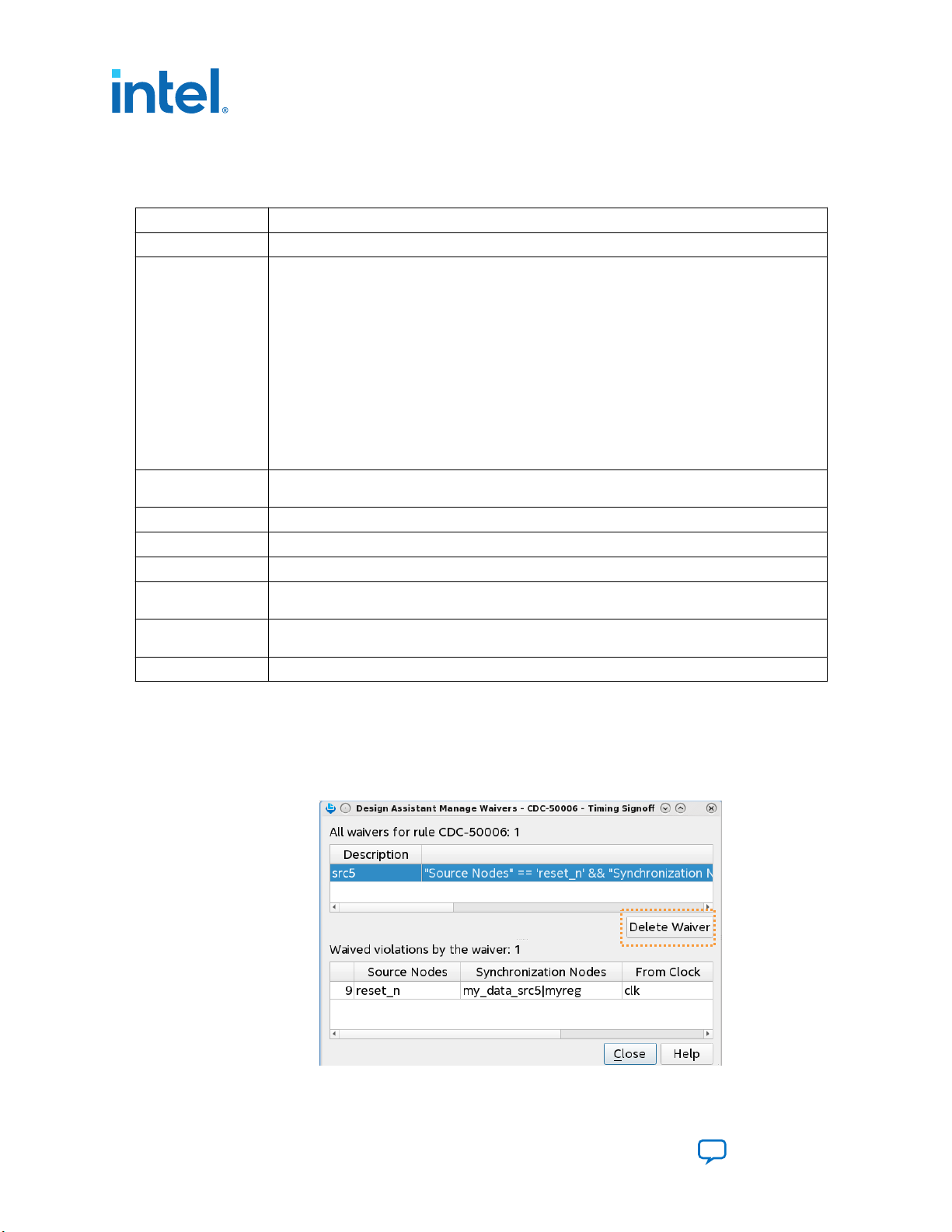
2. Recommended Design Practices
UG-20131 | 2021.03.29
The following table shows the Design Assistant Waiver dialog box options:
Table 5. Design Assistant Waiver Dialog Box Options
Setting Description
Rule conditions Automatically specifies the alphanumeric Rule ID and Compiler Stage of the rule violation.
Violation
conditions
Add Condition Click the Add Condition button to add more conditions to the rule waiver definition. Clicking the
Owner Specifies the waiver owner's ID.
Tag Specifies an identifying tag for the rule waiver.
Description Required value that specifies a text description of the waiver for tracking and identifying.
Preview button Previews the rule violations waived during the next Design Assistant run in the Waived by the
Waived violations
by the waiver
All violations Lists all violations of the currently selected Design Assistant rule.
Specifies the conditions that define a rule violation waiver. The default Violation conditions
automatically reflect the currently selected rule violation from the report. The available condition
attributes are context-sensitive:
• ==is equal to
• != is not equal to
• < is less than
• > is greater than
• <= is less than or equal to
• >= is greater than or equal to
• ! is a negative unary operator for boolean expressions
• =~—string contains
• !~—string does not contain
The join operators between conditions are always AND.
button adds a condition of default type.
waiver field.
Upon clicking the Preview button, lists the rule violations that are waived during the next Design
Assistant run.
2.5.5.5.2. Deleting Design Assistant Waivers
To fully remove (delete) any Design Assistant waivers that are no longer useful, delete
the waiver in the Design Assistant Manage Waivers dialog box.
Figure 44. Design Assistant Manage Waivers Dialog Box
Intel Quartus Prime Pro Edition User Guide: Design Recommendations
100
Send Feedback
 Loading...