

Page 1

Intel® Quark SoC X1000 Core
Developer’s Manual
October 2013
Order Number: 329679-001US
Page 2

Legal Lines and Disclaimers
INFORMATION IN THIS DOCUMENT IS PROVIDED IN CONNECTION WITH INTEL PRODUCTS. NO LICENSE , E XPRESS OR IMPLIED, BY ESTOPPEL OR
OTHERWISE, TO ANY INTELLECTUAL PROPERTY RIGHTS IS GRANTED BY THIS DOCUMENT. EXCEPT AS PROVIDED IN INTEL'S TERMS AND CONDITIONS
OF SALE FOR SUCH PRODUCTS, INTEL ASSUMES NO LIABILITY WHATSOEVER AND INTEL DISCLAIMS ANY EXPRESS OR IMPLIED WARRANTY, RELA TING
TO SALE AND/OR USE OF INTEL PRODUCTS INCLUDING LIABILITY OR WARRANTIES RELATING TO FITNESS FOR A PARTICULAR PURPOSE,
MERCHANTABILITY, OR INFRINGEMENT OF ANY PATENT, COPYRIGHT OR OTHER INTELLECTUAL PROPERTY RIGHT.
A "Mission Critical Application" is any application in which failure of the Intel Product could result, directly or indirectly, in personal injury or death.
SHOULD YOU PURCHASE OR USE INTEL'S PRODUCTS FOR ANY SUCH MISSION CRITICAL APPLICATION, YOU SHALL INDEMNIFY AND HOLD INTEL AND
ITS SUBSIDIARIES, SUBCONTRACTORS AND AFFILIATES, AND THE DIRECTORS, OFFICERS, AND EMPLOYEES OF EACH, HARMLESS AGAINST ALL
CLAIMS COSTS, DAMAGES, AND EXPENSES AND REASONABLE ATTORNEYS' FEES ARISING OUT OF , DIRECTL Y OR INDIRECTL Y, ANY CLAIM OF PRODUCT
LIABILITY, PERSONAL INJURY, OR DEATH ARISING IN ANY WAY OUT OF SUCH MISSION CRITICAL APPLICATION, WHETHER OR NOT INTEL OR ITS
SUBCONTRACTOR WAS NEGLIGENT IN THE DESIGN, MANUFACTURE, OR WARNING OF THE INTEL PRODUCT OR ANY OF ITS PARTS.
Intel may make changes to specifications and product descriptions at any time, without notice. Designers must not rely on the absence or characteristics
of any features or instructions marked "reserved" or "undefined". Intel reserves these for future definition and shall have no responsibility whatsoever
for conflicts or incompatibilities arising from future changes to them. The information here is subject to change without notice. Do not finalize a design
with this information.
The products described in this document may contain design defects or errors known as errata which may cause the product to deviate from published
specifications. Current characterized errata are available on request.
Contact your local Intel sales office or your distributor to obtain the latest specifications and before placing your product order.
Copies of documents which have an order number and are referenced in this document, or other Intel literature, may be obtained by calling 1-800-548-
4725, or go to: http://www.intel.com/design/literature.htm
Any software source code reprinted in this document is furnished for informational purposes only and may only be used or copied and no license, express
or implied, by estoppel or otherwise, to any of the reprinted source code is granted by this document.
Intel processor numbers are not a measure of performance. Processor numbers differentiate features within each processor family, not across different
processor families. Go to: http://www.intel.com/products/processor_number/
Code Names are only for use by Intel to identify products, platforms, programs, services, etc. (“products”) in development by Intel that have not been
made commercially available to the public, i.e., announced, launched or shipped. They are never to be used as “commercial” names for products. Also,
they are not intended to function as trademarks.
Intel and the Intel logo are trademarks of Intel Corporation in the U.S. and/or other countries.
*Other names and brands may be claimed as the property of others.
Copyright © 2013, Intel Corporation. All rights reserved.
Intel® Quark SoC X1000 Core
Developer’s Manual October 2013
2 Order Number: 329679-001US
Page 3

Revision History—Intel
®
Quark Core
Revision History
Date Revision Description
September 2013 001 First external release of document.
October 2013 Developer’s Manual
Order Number: 329679-001US 3
Intel® Quark SoC X1000 Core
Page 4

Intel® Quark Core—Contents
Contents
1.0 About this Manual.......................................................................................................17
1.1 Manual Contents............................... .. .. ......................... .. ... ...............................17
1.2 Notation Conventions.........................................................................................18
1.3 Special Terminology.................................... .. ... ........................... .......................19
1.4 Related Documents................................. .. .. .......................... .. .. .........................20
2.0 Intel® Quark SoC X1000 Core Overview.........................................................................21
2.1 Intel
3.0 Architectural Overview.................................................................................................22
3.1 Internal Architecture............................. .. ............................ ........................... ....22
3.2 System Architecture...................................................................... .. .. .................22
3.3 Memory Organization .........................................................................................22
3.4 I/O Space.........................................................................................................25
3.5 Addressing Modes..............................................................................................25
3.6 Data Types .......................................................................................................28
3.7 Interrupts.........................................................................................................33
4.0 System Register Organization.......................................................................................39
4.1 Register Set Overview................... .....................................................................39
4.2 Floating-Point Registers......................................................................................39
4.3 Base Architecture Registers.................................................................. ... .. ..........39
4.4 System-Level Registers ......................................................................................45
®
Quark Core Architecture..................................................... .. .....................21
3.3.1 Address Spaces......................................................................................23
3.3.2 Segment Register Usage..........................................................................24
3.5.1 Addressing Modes Overview.....................................................................25
3.5.2 Register and Immediate Modes.................................... ........................... ..26
3.5.3 32-Bit Memory Addressing Modes .............................................................26
3.5.4 Differences Between 16- and 32-Bit Addresses ...........................................28
3.6.1 Data Types ............................................................................................28
3.6.1.1 Unsigned Data Types.................................................................29
3.6.1.2 Signed Data Types ....................................................................29
3.6.1.3 BCD Data Types.................................. .......................... .. .. ........30
3.6.1.4 Floating-Point Data Types...........................................................30
3.6.1.5 String Data Types ................................................ .. ...................30
3.6.1.6 ASCII Data Types........................ ..............................................31
3.6.1.7 Pointer Data Types....................................................................32
3.6.2 Little Endian vs. Big Endian Data Formats ..................................................33
3.7.1 Interrupts and Exceptions........................................................................33
3.7.2 Interrupt Processing................................................................................34
3.7.3 Maskable Interrupt..................................................................................34
3.7.4 Non-Maskable Interrupt...........................................................................35
3.7.5 Software Interrupts.................................................................................36
3.7.6 Interrupt and Exception Priorities..............................................................36
3.7.7 Instruction Restart..................................................................................37
3.7.8 Double Fault ..........................................................................................38
3.7.9 Floating-Point Interrupt Vectors................................................................38
4.3.1 General Purpose Registers .......................................................................40
4.3.2 Instruction Pointer..................................................................................41
4.3.3 Flags Register ........................................................................................41
4.3.4 Segment Registers..................................................................................44
4.3.5 Segment Descriptor Cache Registers.........................................................44
4.4.1 Control Registers....................................................................................46
®
Quark SoC X1000 Core
Intel
Developer’s Manual October 2013
4 Order Number: 329679-001US
Page 5

Contents—Intel
®
Quark Core
4.4.1.1 Control Register 0 (CR0)............................................................47
4.4.1.2 Control Register 1 (CR1)............................................................51
4.4.1.3 Control Register 2 (CR2)............................................................51
4.4.1.4 Control Register 3 (CR3)............................................................51
4.4.1.5 Control Register 4 (CR4)............................................................51
4.4.2 System Address Registers .......................................................................52
4.5 Floating-Point Registers......................................................................................53
4.5.1 Floating-Point Data Registers...................................................................53
4.5.2 Floating-Point Tag Word..........................................................................54
4.5.3 Floating-Point Status Word......................................................................54
4.5.4 Instruction and Data Pointers...................................................................58
4.5.5 FPU Control Word...................................................................................61
4.6 Debug and Test Registers...................................................................................62
4.6.1 Debug Registers.....................................................................................62
4.6.2 Test Registers........................................................................................62
4.7 Register Accessibility .........................................................................................62
4.7.1 FPU Register Usage ................................................................................63
4.8 Reserved Bits and Software Compatibility.............................................................63
4.9 Intel
®
Quark Core Model Specific Registers (MSRs)................................................64
5.0 Real Mode Architecture................................................................................................65
5.1 Introduction .....................................................................................................65
5.2 Memory Addressing....................................................... ............................ ........66
5.3 Reserved Locations............................................................................................66
5.4 Interrupts ........................................................................................................67
5.5 Shutdown and Halt.............................................. ........................... ...................67
6.0 Protected Mode Architecture ........................................................................................68
6.1 Addressing Mechanism.......................................................................................68
6.2 Segmentation...................................................................................................69
6.2.1 Segmentation Introduction ............................................. .. .. .. .. .................69
6.2.2 Terminology ..........................................................................................70
6.2.3 Descriptor Tables ...................................................................................70
6.2.3.1 Descriptor Tables Introduction....................................................70
6.2.3.2 Global Descriptor Table..................................... .........................71
6.2.3.3 Local Descriptor Table ................................ .. .. ...........................71
6.2.3.4 Interrupt Descriptor Table............................... .. .. .......................71
6.2.4 Descriptors............................................................................................72
6.2.4.1 Descriptor Attribute Bits ............................................................72
6.2.4.2 Intel
®
Quark Core Code, Data Descriptors (S=1) ..........................72
6.2.4.3 System Descriptor Formats ........................................................74
6.2.4.4 LDT Descriptors (S=0, TYPE=2)..................................................75
6.2.4.5 TSS Descriptors (S=0, TYPE=1, 3, 9, B) ......................................75
6.2.4.6 Gate Descriptors (S=0, TYPE=4–7, C, F)......................................75
6.2.4.7 Selector Fields..........................................................................77
6.2.4.8 Segment Descriptor Cache.........................................................77
6.2.4.9 Segment Descriptor Register Settings..........................................77
6.3 Protection ........................................................................................................81
6.3.1 Protection Concepts................................................................................81
6.3.2 Rules of Privilege....................................................................................82
6.3.3 Privilege Levels......................................................................................82
6.3.3.1 Task Privilege...........................................................................82
6.3.3.2 Selector Privilege (RPL) .............................................................82
6.3.3.3 I/O Privilege and I/O Permission Bitmap ......................................83
6.3.3.4 Privilege Validation....................................................................85
6.3.3.5 Descriptor Access .....................................................................85
6.3.4 Privilege Level Transfers..........................................................................86
October 2013 Developer’s Manual
Order Number: 329679-001US 5
Intel® Quark SoC X1000 Core
Page 6

Intel® Quark Core—Contents
6.3.5 Call Gates..............................................................................................87
6.3.6 Task Switching............................ .. ............................ .............................88
6.3.6.1 Floating-Point Task Switching......................................................89
6.3.7 Initialization and Transition to Protected Mode............................................89
6.4 Paging..............................................................................................................91
6.4.1 Paging Concepts.....................................................................................91
6.4.2 Paging Organization................................................................................91
6.4.2.1 Page Mechanism .......................................................................91
6.4.2.2 Page Descriptor Base Register.................................... .. ...............91
6.4.2.3 Page Directory..........................................................................92
6.4.2.4 Page Tables..............................................................................92
6.4.2.5 Page Directory/Table Entries.......................................................92
6.4.2.6 Paging-Mode Modifiers ................................... .. .........................92
6.4.3 PAE Paging ............................................................................................93
6.4.3.1 PDPTE Registers........................................................................93
6.4.3.2 Linear-Address Translation with PAE Paging..................................94
6.4.4 #GP Faults for Intel
®
Quark SoC X1000 Core ..........................................100
6.4.5 Access Rights ......................................................................................100
6.4.5.1 SMEP Details for Intel® Quark SoC X1000 Core...........................101
6.4.6 Page Level Protection (R/W, U/S Bits)......................................................102
6.4.7 Page Cacheability (PWT and PCD Bits).....................................................103
6.4.8 Translation Lookaside Buffer ................................................. .................103
6.4.9 Page-Fault Exceptions ............................ ........................... .. .................104
6.4.10 Paging Operation..................................................................................106
6.4.11 Operating System Responsibilities...........................................................107
6.5 Virtual 8086 Environment ..................................................... .. .... .. .... .. .. ............10 7
6.5.1 Executing Programs..............................................................................107
6.5.2 Virtual 8086 Mode Addressing Mechanism ......... .......................................108
6.5.3 Paging in Virtual Mode...........................................................................108
6.5.4 Protection and I/O Permission Bitmap......................................................109
6.5.5 Interrupt Handling................................................................................110
6.5.6 Entering and Leaving Virtual 8086 Mode ........... .. .. ...................................111
6.5.6.1 Task Switches to and from Virtual 8086 Mode ............................ .112
6.5.6.2 Transitions Through Trap and Interrupt Gates, and IRET...............112
7.0 On-Chip Cache .........................................................................................................114
7.1 Cache Organization..........................................................................................114
7.1.1 Write-Back Enhanced Intel
7.2 Cache Control .................................................................................................116
7.2.1 Write-Back Enhanced Intel
®
Quark SoC X1000 Core Cache ........................115
®
Quark SoC X1000 Core Cache Control and
Operating Modes ..................................................................................116
7.3 Cache Line Fills................................................................................................117
7.4 Cache Line Invalidations...................................................................................118
7.4.1 Write-Back Enhanced Intel
®
Quark SoC X1000 Core Snoop Cycles and
Write-Back Mode Invalidation..................... .. .. .. .. ....................................118
7.5 Cache Replacement..........................................................................................118
7.6 Page Cacheability ............................................................................................119
7.6.1 Write-Back Enhanced Intel
®
Quark SoC X1000 Core and Processor Page
Cacheability.........................................................................................121
7.7 Cache Flushing................................................................................................122
7.7.1 Write-Back Enhanced Intel
7.8 Write-Back Enhanced Intel
®
7.8.1 Write-Back Cache Coherency Protocol......................................................123
7.8.2 Detecting On-Chip Write-Back Cache of the Write-Back Enhanced Intel
®
Quark SoC X1000 Core Cache Flushing............122
Quark SoC X1000 Core Write-Back Cache Architecture .123
®
Quark SoC X1000 Core..........................................................................125
8.0 System Management Mode (SMM) Architectures ...........................................................127
®
Quark SoC X1000 Core
Intel
Developer’s Manual October 2013
6 Order Number: 329679-001US
Page 7

Contents—Intel
®
Quark Core
8.1 SMM Overview................................................................................................ 127
8.2 Terminology ................................................................................................... 127
8.3 System Management Interrupt Processing.......................................................... 128
8.3.1 System Management Interrupt (SMI#).................................................... 129
8.3.2 SMI# Active (SMIACT#)........................................................................ 129
8.3.3 SMRAM............................................................................................... 130
8.3.3.1 SMRAM State Save Map........................................................... 131
8.3.4 Exit From SMM..................................................................................... 133
8.4 System Management Mode Programming Model .................................................. 134
8.4.1 Entering System Management Mode ....................................................... 134
8.4.2 Processor Environment.......................................................................... 135
8.4.2.1 Write-Back Enhanced Intel
®
Quark SoC X1000 Core Environment . 136
8.4.3 Executing System Management Mode Handler.................................. .. .. .... 136
8.4.3.1 Exceptions and Interrupts within System Management Mode ........ 137
8.5 SMM Features................................................................................................. 138
8.5.1 SMM Revision Identifier......................................................................... 138
8.5.2 Auto Halt Restart ................................................................................. 138
8.5.3 I/O Instruction Restart.......................................................................... 139
8.5.4 SMM Base Relocation............................................................................ 140
8.6 SMM System Design Considerations................................................................... 141
8.6.1 SMRAM Interface.................................................................................. 141
8.6.2 Cache Flushes.................................................................................... .. 142
8.6.2.1 Write-Back Enhanced Intel
®
Quark SoC X1000 Core System
Management Mode and Cache Flushing...................................... 144
8.6.2.2 Snoop During SMM.................... .. ............................................ 146
8.6.3 A20M# Pin and SMBASE Relocation ........................................................ 146
8.6.4 Processor Reset During SMM.................................................................. 146
8.6.5 SMM and Second-Level Write Buffers...................................................... 147
8.6.6 Nested SMI#s and I/O Restart ............................................................... 147
8.7 SMM Software Considerations........................................................................... 147
8.7.1 SMM Code Considerations...................................................................... 147
8.7.2 Exception Handling................................. ........................... ................... 148
8.7.3 Halt During SMM.................................................................................. 148
8.7.4 Relocating SMRAM to an Address Above One Megabyte ............................. 148
9.0 Hardware Interface................................................................................................... 149
9.1 Introduction ................................................................................................... 149
9.2 Signal Descriptions.......................................... .. ........................... ................... 150
9.2.1 Clock (CLK)......................................................................................... 150
9.2.2 Address Bus (A[31:2], BE[3:0]#)........................................................... 150
9.2.3 Data Lines (D[31:0]) ............................................................................ 151
9.2.4 Parity ................................................................................................. 151
9.2.4.1 Data Parity Input/Outputs (DP[3:0]) ......................................... 151
9.2.4.2 Parity Status Output (PCHK#) .................................................. 151
9.2.5 Bus Cycle Definition.............................................................................. 152
9.2.5.1 M/IO#, D/C#, W/R# Outputs ................................................... 152
9.2.5.2 Bus Lock Output (LOCK#)........................................................ 152
9.2.5.3 Pseudo-Lock Output (PLOCK#)................................................. 153
9.2.5.4 PLOCK# Floating-Point Considerations ....................................... 153
9.2.6 Bus Control ......................................................................................... 153
9.2.6.1 Address Status Output (ADS#)................................................. 153
9.2.6.2 Non-Burst Ready Input (RDY#).......................... .. .. .. .. ... ............ 153
9.2.7 Burst Control....................................................................................... 154
9.2.7.1 Burst Ready Input (BRDY#) ..................................................... 154
9.2.7.2 Burst Last Output (BLAST#)..................................................... 154
9.2.8 Interrupt Signals.................................................................................. 154
October 2013 Developer’s Manual
Order Number: 329679-001US 7
Intel® Quark SoC X1000 Core
Page 8

Intel® Quark Core—Contents
9.2.8.1 Reset Input (RESET).......................... .. .. .. ............................ ....154
9.2.8.2 Soft Reset Input (SRESET) .......................................................155
9.2.8.3 System Management Interrupt Request Input (SMI#)..................155
9.2.8.4 System Management Mode Active Output (SMIACT#) ..................155
9.2.8.5 Maskable Interrupt Request Input (INTR) ............................... .. ..155
9.2.8.6 Non-maskable Interrupt Request Input (NMI)..............................156
9.2.8.7 Stop Clock Interrupt Request Input (STPCLK#) ...........................156
9.2.9 Bus Arbitration Signals ..........................................................................156
9.2.9.1 Bus Request Output (BREQ).................... .. ... .. ...........................156
9.2.9.2 Bus Hold Request Input (HOLD) ................................................156
9.2.9.3 Bus Hold Acknowledge Output (HLDA)........................................157
9.2.9.4 Backoff Input (BOFF#).............................................................157
9.2.10 Cache Invalidation................................................................................157
9.2.10.1 Address Hold Request Input (AHOLD) ........................................158
9.2.10.2 External Address Valid Input (EADS#)........................................158
9.2.11 Cache Control ......................................................................................158
9.2.11.1 Cache Enable Input (KEN#)....................................... .. ... .. ........158
9.2.11.2 Cache Flush Input (FLUSH#).....................................................158
9.2.12 Page Cacheability (PWT, PCD) ................................................................159
9.2.13 RESERVED#.........................................................................................159
9.2.14 Numeric Error Reporting (FERR#, IGNNE#)..............................................159
9.2.14.1 Floating-Point Error Output (FERR#)..........................................159
9.2.14.2 Ignore Numeric Error Input (IGNNE#)........................................160
9.2.15 Bus Size Control (BS16#, BS8#) ............................................................160
9.2.16 Address Bit 20 Mask (A20M#)................................................................161
9.2.17 Write-Back Enhanced Intel
®
Quark SoC X1000 Core Signals and Other
Enhanced Bus Features .........................................................................161
9.2.17.1 Cacheability (CACHE#) ............................................................161
9.2.17.2 Cache Flush (FLUSH#).................................... .........................162
9.2.17.3 Hit/Miss to a Modified Line (HITM#)...........................................162
9.2.17.4 Soft Reset (SRESET)................................................................163
9.2.17.5 Invalidation Request (INV) ................................ .. .....................163
9.2.17.6 Write-Back/Write-Through (WB/WT#)........................................164
9.2.17.7 Pseudo-Lock Output (PLOCK#)....................... .. .. .. .....................164
9.2.18 Test Signals.........................................................................................164
9.2.18.1 Test Clock (TCK)................................. ....................................164
9.2.18.2 Test Mode Select (TMS) ...........................................................165
9.2.18.3 Test Data Input (TDI) ....................................... .. .. .. .................165
9.2.18.4 Test Data Output (TDO)...........................................................165
9.3 Interrupt and Non-Maskable Interrupt Interface...................................................165
9.3.1 Interrupt Logic .....................................................................................166
9.3.2 NMI Logic............................................................................................166
9.3.3 SMI# Logic..........................................................................................166
9.3.4 STPCLK# Logic.....................................................................................167
9.4 Write Buffers...................................................................................................167
9.4.1 Write Buffers and I/O Cycles ..................................................................169
9.4.2 Write Buffers on Locked Bus Cycles.........................................................169
9.5 Reset and Initialization.....................................................................................169
9.5.1 Floating-Point Register Values ................................................................170
9.5.2 Pin State During Reset ..........................................................................171
9.5.2.1 Controlling the CLK Signal in the Processor during Power On.........173
9.5.2.2 FERR# Pin State During Reset for Intel
®
Quark SoC X1000 Core ...173
9.5.2.3 Power Down Mode (In-circuit Emulator Support)..........................174
9.6 Clock Control ..................................................................................................174
9.6.1 Stop Grant Bus Cycles...........................................................................174
9.6.2 Pin State During Stop Grant...................................................................175
®
Quark SoC X1000 Core
Intel
Developer’s Manual October 2013
8 Order Number: 329679-001US
Page 9

Contents—Intel
®
Quark Core
9.6.3 Write-Back Enhanced Intel® Quark SoC X1000 Core Pin States During Stop
Grant State ......................................................................................... 176
9.6.4 Clock Control State Diagram.................................................................. 177
9.6.4.1 Normal State.......................................................................... 177
9.6.4.2 Stop Grant State .................................................................... 177
9.6.4.3 Stop Clock State..................................................................... 179
9.6.4.4 Auto HALT Power Down State................................................... 179
9.6.4.5 Stop Clock Snoop State (Cache Invalidations)............................. 179
9.6.4.6 Auto Idle Power Down State..................................................... 180
9.6.5 Write-Back Enhanced Intel
®
Quark SoC X1000 Core Clock Control State
Diagram.............................................................................................. 180
9.6.5.1 Normal State.......................................................................... 180
9.6.5.2 Stop Grant State .................................................................... 181
9.6.5.3 Stop Clock State..................................................................... 182
9.6.5.4 Auto HALT Power Down State................................................... 182
9.6.6 Stop Clock Snoop State (Cache Invalidations) .......................................... 183
9.6.6.1 Auto HALT Power Down Flush State (Cache Flush) for the
Write-Back Enhanced Intel
®
Quark SoC X1000 Core.................... 183
10.0 Bus Operation.......................................................................................................... 184
10.1 Data Transfer Mechanism................................................................................. 184
10.1.1 Memory and I/O Spaces......................................... .. .. .. ......................... 184
10.1.1.1 Memory and I/O Space Organization ......................................... 185
10.1.2 Dynamic Data Bus Sizing....................................................................... 186
10.1.3 Interfacing with 8-, 16-, and 32-Bit Memories.......................................... 187
10.1.4 Dynamic Bus Sizing during Cache Line Files............................................. 191
10.1.5 Operand Alignment............................................................................... 192
10.2 Bus Arbitration Logic........................................................................................ 193
10.3 Bus Functional Description................................................................................ 196
10.3.1 Non-Cacheable Non-Burst Single Cycles .................................................. 196
10.3.1.1 No Wait States ....................................................................... 196
10.3.1.2 Inserting Wait States....................... .. ............................ .. ........ 197
10.3.2 Multiple and Burst Cycle Bus Transfers....................... ............................. 198
10.3.2.1 Burst Cycles........................................................................... 198
10.3.2.2 Terminating Multiple and Burst Cycle Transfers........................... 199
10.3.2.3 Non-Cacheable, Non-Burst, Multiple Cycle Transfers.................... 200
10.3.2.4 Non-Cacheable Burst Cycles..................................................... 200
10.3.3 Cacheable Cycles ................................................................................. 201
10.3.3.1 Byte Enables during a Cache Line Fill......................................... 202
10.3.3.2 Non-Burst Cacheable Cycles................................................... .. 202
10.3.3.3 Burst Cacheable Cycles............................................................ 203
10.3.3.4 Effect of Changing KEN# during a Cache Line Fill ........................ 204
10.3.4 Burst Mode Details ............................................................................... 205
10.3.4.1 Adding Wait States to Burst Cycles............................................ 205
10.3.4.2 Burst and Cache Line Fill Order................................................. 206
10.3.4.3 Interrupted Burst Cycles.......................................................... 207
10.3.5 8- and 16-Bit Cycles............................................................................. 209
10.3.6 Locked Cycles.............................................. .. ...................................... 211
10.3.7 Pseudo-Locked Cycles........................................................................... 212
10.3.7.1 Floating-Point Read and Write Cycles......................................... 213
10.3.8 Invalidate Cycles.................................................................................. 213
10.3.8.1 Rate of Invalidate Cycles ......................................................... 215
10.3.8.2 Running Invalidate Cycles Concurrently with Line Fills.................. 215
10.3.9 Bus Hold............................................................................................. 217
10.3.10Interrupt Acknowledge.......................................................................... 219
10.3.11 Special Bus Cycles................................................................................ 220
10.3.11.1HALT Indication Cycle............................ ............................ ...... 220
October 2013 Developer’s Manual
Order Number: 329679-001US 9
Intel® Quark SoC X1000 Core
Page 10

Intel® Quark Core—Contents
10.3.11.2Shutdown Indication Cycle .......................................................221
10.3.11.3Stop Grant Indication Cycle......................................................221
10.3.12Bus Cycle Restart .................................................................................222
10.3.13Bus States ...........................................................................................224
10.3.14Floating-Point Error Handling for the Intel
10.3.14.1Floating-Point Exceptions .........................................................225
®
10.3.15Intel
Quark SoC X1000 Core Floating-Point Error Handling in
AT-Compatible Systems.........................................................................226
10.4 Enhanced Bus Mode Operation for the Write-Back Enhanced Intel
®
Quark SoC X1000 Core.............225
®
Quark SoC X1000
Core .............................................................................................................. 226
10.4.1 Summary of Bus Differences ..................................................................226
10.4.2 Burst Cycles.........................................................................................227
10.4.2.1 Non-Cacheable Burst Operation.................................................227
10.4.2.2 Burst Cycle Signal Protocol.......................................................228
10.4.3 Cache Consistency Cycles ......................................................................228
10.4.3.1 Snoop Collision with a Current Cache Line Operation....................229
10.4.3.2 Snoop under AHOLD................................................................230
10.4.3.3 Snoop During Replacement Write-Back ......................................234
10.4.3.4 Snoop under BOFF# ................................................................235
10.4.3.5 Snoop under HOLD..................................................................237
10.4.3.6 Snoop under HOLD during Replacement Write-Back.....................239
10.4.4 Locked Cycles ......................................................................................239
10.4.4.1 Snoop/Lock Collision................................................................241
10.4.5 Flush Operation....................................................................................241
10.4.6 Pseudo Locked Cycles............................................................................242
10.4.6.1 Snoop under AHOLD during Pseudo-Locked Cycles.......................242
10.4.6.2 Snoop under HOLD during Pseudo-Locked Cycles.........................243
10.4.6.3 Snoop under BOFF# Overlaying a Pseudo-Locked Cycle................244
11.0 Debugging Support...................................................................................................246
11.1 Breakpoint Instruction......................................................................................246
11.2 Single-Step Trap.................. ............................ ........................... .....................246
11.3 Debug Registers......................... .. ......................... .. ......................... .. ... ..........246
11.3.1 Linear Address Breakpoint Registers (DR[3:0]).........................................247
11.3.2 Debug Control Register (DR7) .............................. .. ... .. ...........................247
11.3.3 Debug Status Register (DR6) ........................... .. .. .. ................................250
11.3.4 Use of Resume Flag (RF) in Flag Register.................................................251
12.0 Instruction Set Summary...........................................................................................252
12.1 Instruction Set ................................................................................................252
12.1.1 Floating-Point Instructions .....................................................................253
12.2 Instruction Encoding ........................................................................................253
12.2.1 Overview.............................................................................................253
12.2.2 32-Bit Extensions of the Instruction Set...................................................254
12.2.3 Encoding of Integer Instruction Fields......................................................255
12.2.3.1 Encoding of Operand Length (w) Field........................................255
12.2.3.2 Encoding of the General Register (reg) Field ...............................255
12.2.3.3 Encoding of the Segment Register (sreg) Field ............................256
12.2.3.4 Encoding of Address Mode........................................................257
12.2.3.5 Encoding of Operation Direction (d) Field....................................260
12.2.3.6 Encoding of Sign-Extend (s) Field..............................................261
12.2.3.7 Encoding of Conditional Test (tttn) Field .....................................261
12.2.3.8 Encoding of Control or Debug or Test Register (eee) Field.............261
12.2.4 Encoding of Floating-Point Instruction Fields.............................................262
12.2.5 Intel
®
Quark SoC X1000 Core Instructions...............................................263
12.2.5.1 CMPXCHG8B - Compare and Exchange Bytes..............................263
12.2.5.2 RDMSR ..................................................................................264
®
Quark SoC X1000 Core
Intel
Developer’s Manual October 2013
10 Order Number: 329679-001US
Page 11

Contents—Intel
®
Quark Core
12.2.5.3 RDTSC .................................................................................. 264
12.2.5.4 WRMSR ................................................................................. 264
12.3 Clock Count Summary ..................................................................................... 265
12.3.1 Instruction Clock Count Assumptions ...................................................... 265
A Signal Descriptions.............................. ........................... ........................... ............... 291
B Testability ............................................................................................................... 296
B.1 On-Chip Cache Testing..................................................................................... 296
B.1.1 Cache Testing Registers TR3, TR4 and TR5.............................................. 296
B.1.2 Cache Testability Write ......................................................................... 297
B.1.3 Cache Testability Read.......................................................................... 298
B.1.4 Flush Cache............... ... .. ..................................................................... 299
B.1.5 Additional Cache Testing Features for Write-Back Enhanced Intel® Quark
SoC X1000 Core................................................................................... 299
B.2 Translation Lookaside Buffer (TLB) Testing ......................................................... 300
B.2.1 Translation Lookaside Buffer Organization................................................ 300
B.2.2 TLB Test Registers TR6 and TR7............................................................. 301
B.2.2.1 Command Test Register: TR6........................ ........................... 301
B.2.2.2 Data Test Register: TR7........................................................... 303
B.2.3 TLB Write Test ..................................................................................... 303
B.2.4 TLB Lookup Test .................................................................................. 304
®
B.3 Intel
Quark SoC X1000 Core JTAG................................................................... 304
B.3.1 Test Access Port (TAP) Controller ........................................................... 304
B.3.1.1 Test-Logic-Reset State ............................................................ 305
B.3.1.2 Run-Test/Idle State................................................................. 305
B.3.1.3 Select-DR-Scan State.............................................................. 305
B.3.1.4 Capture-DR State ................................................................... 306
B.3.1.5 Shift-DR State........................................................................ 306
B.3.1.6 Exit1-DR State .................................................. .. ................... 306
B.3.1.7 Pause-DR State...................................................................... 306
B.3.1.8 Exit2-DR State .................................................. .. ................... 306
B.3.1.9 Update-DR State .................................................................... 307
B.3.1.10 Select-IR-Scan State............................................................... 307
B.3.1.11 Capture-IR State .................................................................... 307
B.3.1.12 Shift-IR State......................................................................... 307
B.3.1.13 Exit1-IR State ........................................................................ 307
B.3.1.14 Pause-IR State....................................................................... 307
B.3.1.15 Exit2-IR State ........................................................................ 308
B.3.1.16 Update-IR State ..................................................................... 308
B.3.2 TAP Controller Initialization.................................................................... 308
C Feature Determination .............................................................................................. 309
C.1 CPUID Instruction ........................................................................................... 309
C.2 Intel
®
Quark SoC X1000 Stepping..................................................................... 311
Figures
1Intel® Quark SoC X1000 Core used in Intel® Quark SoC X1000 .....................................21
2 Address Translation......................... .. ........................... ........................... .................24
3 Addressing Mode Calculations....................................................................................27
4 Data Types ............................. ................................................... .. .. .........................29
5 Data Types ............................. ................................................... .. .. .........................31
6 String and ASCII Data Types.....................................................................................32
7 Pointer Data Types................................ .. ........................... ............................ ..........32
8 Big vs. Little Endian Memory Format...........................................................................33
October 2013 Developer’s Manual
Order Number: 329679-001US 11
Intel® Quark SoC X1000 Core
Page 12

Intel® Quark Core—Contents
9 Base Architecture Registers .......................................................................................40
10 Flag Registers..........................................................................................................41
11 Intel
®
Quark SoC X1000 Core Segment Registers and Associated Descriptor Cache
Registers.................................................................................................................45
12 System-Level Registers.............................................................................................46
13 Control Registers .....................................................................................................47
14 Intel
®
Quark SoC X1000 Core CR4 Register.................................................................52
15 Floating-Point Registers.............................................................................................53
16 Floating-Point Tag Word............................................................................................54
17 Floating-Point Status Word ........................................................................................55
18 Protected Mode FPU Instructions and Data Pointer Image in Memory (32-Bit Format) ........59
19 Real Mode FPU Instruction and Data Pointer Image in Memory (32-Bit Format).................59
20 Protected Mode FPU Instruction and Data Pointer Image in Memory (16-Bit Format)..........60
21 Real Mode FPU Instruction and Data Pointer Image in Memory (16-Bit Format).................60
22 FPU Control Word.....................................................................................................61
23 Real Address Mode Addressing...................................................................................66
24 Protected Mode Addressing........................................................................................69
25 Paging and Segmentation..........................................................................................69
26 Descriptor Table Registers.........................................................................................71
27 Interrupt Descriptor Table Register Use.......................................................................72
28 Segment Descriptors..................... .. ... ........................... .. ........................... ...............73
29 System Segment Descriptors .....................................................................................75
30 Gate Descriptor Formats............................................................................................76
31 Example Descriptor Selection.................. .. .. .. ........................... ... .. ........................... ..78
32 Segment Descriptor Caches for Real Address Mode (Segment Limit and Attributes Are
Fixed).....................................................................................................................79
33 Segment Descriptor Caches for Protected Mode (Loaded per Descriptor) ..........................80
34 Segment Descriptor Caches for Virtual 8086 Mode within Protected Mode (Segment Limit
and Attributes are Fixed)................................................................ ...........................81
35 Four-Level Hierarchical Protection...............................................................................82
36 Intel
37 Sample I/O Permission Bit Map ..................................................................................85
38 Intel
®
Quark Core TSS and TSS Registers....................................................................84
®
Quark Core TSS .............................................................................................88
39 Simple Protected System........................................... ........................... .. ...................90
40 GDT Descriptors for Simple System.................. ............................ .. .. .. .........................91
41 Linear-Address Translation to a 4-KByte Page using PAE Paging......................................95
42 Linear-Address Translation to a 2-MByte Page using PAE Paging .....................................96
43 Formats of CR3 and Paging-Structure Entries in 32-bit Mode with PAE Paging Disabled ......98
44 Formats of CR3 and Paging-Structure Entries in 32-bit Mode with PAE Paging Enabled.......99
45 Translation Lookaside Buffer ....................................................................................104
46 Page-Fault Error Code.............................................................................................105
47 Page Fault System Information...................... .. .........................................................107
48 Virtual 8086 Environment Memory Management .........................................................108
49 Virtual 8086 Environment Interrupt and Call Handling .................................................111
50 On-Chip Cache Physical Organization ........................................................................114
51 On-Chip Cache Replacement Strategy.......................................................................119
52 Page Cacheability ...................................................................................................121
53 Basic SMI# Interrupt Service ...................................................................................128
54 Basic SMI# Hardware Interface................................................................................129
55 SMI# Timing for Servicing an I/O Trap......................................................................130
56 Intel
®
Quark SoC X1000 Core SMIACT# Timing..........................................................130
57 Redirecting System Memory Addresses to SMRAM.......................................................132
58 Transition to and from System Management Mode ......................................................135
59 SMM Revision Identifier...........................................................................................138
60 Auto HALT Restart..................................................................................................139
®
Quark SoC X1000 Core
Intel
Developer’s Manual October 2013
12 Order Number: 329679-001US
Page 13

Contents—Intel
®
Quark Core
61 I/O Instruction Restart............................................................................................ 139
62 SMM Base Location ................................................................................................ 140
63 SMRAM Usage .................................... ......................... .. .. ...................................... 141
64 SMRAM Location ............................. ........................... ........................... ................. 142
65 FLUSH# Mechanism during SMM........................................................... .. .. ............... 143
66 Cached SMM ......................................................................................................... 143
67 Non-Cached SMM................................................................................................... 144
68 Write-Back Enhanced Intel
®
Quark SoC X1000 Core Cache Flushing for Overlaid
SMRAM upon Entry and Exit of Cached SMM.............................................................. 145
69 Functional Signal Groupings .................................................................................... 150
70 Reordering of a Reads with Write Buffers................................................................... 168
71 Reordering of a Reads with Write Buffers................................................................... 168
72 Pin States During RESET......................................................................................... 172
73 Stop Clock Protocol ................................................................................................ 175
74 Intel
75 Recognition of Inputs when Exiting Stop Grant State .................................................. 179
76 Write-Back Enhanced Intel
®
Quark SoC X1000 Core Stop Clock State Machine ............. .. .............................. 178
®
Quark SoC X1000 Core Stop Clock State Machine
(Enhanced
Bus Configuration) ................................................................................................. 181
77 Physical Memory and I/O Spaces.............................................................................. 185
78 Physical Memory and I/O Space Organization............................................................. 186
79 Intel
®
Quark SoC X1000 Core with 32-Bit Memory ..................... .. .... .. .. .... .. ................ 188
80 Addressing 16- and 8-Bit Memories.......................................................................... 188
81 Logic to Generate A1, BHE# and BLE# for 16-Bit Buses .............................................. 190
82 Data Bus Interface to 16- and 8-Bit Memories............................................................ 191
83 Single Master Intel
®
Quark Core System................................................................... 193
84 Single Intel® Quark Core with DMA .......................................................................... 194
85 Single Intel® Quark Core with Multiple Secondary Masters........................................... 195
86 Basic 2-2 Bus Cycle................................................................................................ 197
87 Basic 3-3 Bus Cycle................................................................................................ 198
88 Non-Cacheable, Non-Burst, Multiple-Cycle Transfers................................................... 200
89 Non-Cacheable Burst Cycle...................................................................................... 201
90 Non-Burst, Cacheable Cycles................................................................................... 203
91 Burst Cacheable Cycle ................................... ............................ .. ........................... 204
92 Effect of Changing KEN#......................................................................................... 205
93 Slow Burst Cycle.................................................................................................... 206
94 Burst Cycle Showing Order of Addresses ................................................................... 207
95 Interrupted Burst Cycle........................................................................................... 208
96 Interrupted Burst Cycle with Non-Obvious Order of Addresses...................................... 209
97 8-Bit Bus Size Cycle ............................................................................................... 210
98 Burst Write as a Result of BS8# or BS16#.................................... ........................... .. 211
99 Locked Bus Cycle................................................................................................... 212
100 Pseudo Lock Timing................................................................................................ 213
101 Fast Internal Cache Invalidation Cycle ...................................................................... 214
102 Typical Internal Cache Invalidation Cycle................................................................... 214
103 System with Second-Level Cache............................................................................. 216
104 Cache Invalidation Cycle Concurrent with Line Fill....................................................... 217
105 HOLD/HLDA Cycles................................................................................................. 218
106 HOLD Request Acknowledged during BOFF# .............................................................. 219
107 Interrupt Acknowledge Cycles.................................................................................. 220
108 Stop Grant Bus Cycle.............................................................................................. 221
109 Restarted Read Cycle.............................................................................................. 222
110 Restarted Write Cycle............................................................................................. 223
111 Bus State Diagram................................................................................................. 224
112 Basic Burst Read Cycle ........................................................................................... 227
October 2013 Developer’s Manual
Order Number: 329679-001US 13
Intel® Quark SoC X1000 Core
Page 14

Intel® Quark Core—Contents
113 Snoop Cycle Invalidating a Modified Line ...................................................................231
114 Snoop Cycle Overlaying a Line-Fill Cycle....................................................................232
115 Snoop Cycle Overlaying a Non-Burst Cycle.................................................................233
116 Snoop to the Line that is Being Replaced ...................................................................234
117 Snoop under BOFF# during a Cache Line-Fill Cycle......................................................236
118 Snoop under BOFF# to the Line that is Being Replaced................................................237
119 Snoop under HOLD during Line Fill............................................................................238
120 Snoop using HOLD during a Non-Cacheable, Non-Burstable Code Prefetch .....................239
121 Locked Cycles (Back-to-Back) ............................................ .. .. .. ............................ .. ..240
122 Snoop Cycle Overlaying a Locked Cycle.....................................................................241
123 Flush Cycle.......................................................................... ............................ ......242
124 Snoop under AHOLD Overlaying Pseudo-Locked Cycle .................................................243
125 Snoop under HOLD Overlaying Pseudo-Locked Cycle ...................................................244
126 Snoop under BOFF# Overlaying a Pseudo-Locked Cycle...............................................245
127 Size Breakpoint Fields............................................................................................. 248
128 General Instruction Format .....................................................................................253
129 Intel
130 TR4 Definition for Standard and Enhanced Bus Modes for the Write-Back Enhanced
131 TR5 Definition for Standard and Enhanced Bus Modes for the Write-Back Enhanced
®
Quark SoC X1000 Core Cache Test Registers....................................................296
®
Intel
Quark SoC X1000 Core..................................................................................300
®
Intel
Quark SoC X1000 Core..................................................................................300
132 TLB Organization....................................................................................................301
133 TLB Test Registers..................................................................................................302
134 TAP Controller State Diagram...................................................................................305
Tables
1 Manual Contents ......................................................................................................17
2 Related Documents...................................................................................................20
3 Segment Register Selection Rules............................... .. .. ........................... .. ... ............25
4 BASE and INDEX Registers for 16- and 32-Bit Addresses ...............................................28
5 Interrupt Vector Assignments.....................................................................................35
6 FPU Interrupt Vector Assignments ..............................................................................35
7 Sequence of Exception Checking.................................................................................37
8 Interrupt Vectors Used by FPU ................................................. ... ........................... ....38
9 Data Type Alignment Requirements ............................................................................42
10 Intel
11 On-Chip Cache Control Modes ............................................ ............................ .. .. ........48
12 Recommended Values of the Floating-Point Related Bits for Intel
13 Interpreting Different Combinations of EM, TS and MP Bits.............................................50
14 Condition Code Interpretation after FPREM and FPREM1 Instructions ...............................56
15 Floating-Point Condition Code Interpretation ................................................................56
16 Condition Code Resulting from Comparison..................................................................57
17 Condition Code Defining Operand Class.......................................................................57
18 FPU Exceptions ........................................................................................................58
19 Debug Registers.......................................................................................................62
20 Test Registers..........................................................................................................62
21 Register Usage.........................................................................................................63
22 FPU Register Usage Differences..................................................................................63
23 MSRs for Intel
24 Instruction Forms in which LOCK Prefix Is Legal............................................................65
25 Exceptions with Different Meanings in Real Mode (see Table 24) .....................................67
26 Access Rights Byte Definition for Code and Data Descriptions.........................................74
27 Pointer Test Instructions............................................................................................85
®
Quark SoC X1000 Core Operating Modes............................................................48
®
Quark SoC X1000
Core.......................................................................................................................50
®
Quark Core 1 ....................................................................................64
®
Quark SoC X1000 Core
Intel
Developer’s Manual October 2013
14 Order Number: 329679-001US
Page 15

Contents—Intel
®
Quark Core
28 Descriptor Types Used for Control Transfer..................................................................86
29 Use of CR3 with PAE Paging.......................................................................................93
30 Format of a PAE Page-Directory-Pointer-Table Entry (PDPTE).........................................94
31 Format of a PAE Page-Directory Entry that Maps a 2-MByte Page....................................96
32 Format of a PAE Page-Directory Entry that References a Page Table................................97
33 Format of a PAE Page-Table Entry that Maps a 4-KByte Page .........................................97
34 Page Level Protection Attributes................................. .. .. ........................... ... .. .. ........ 103
35 Write-Back Enhanced Intel
®
Quark SoC X1000 Core WB/WT# Initialization.................... 115
36 Cache Operating Modes .......................................................................................... 116
37 Write-Back Enhanced Intel® Quark SoC X1000 Core Write-Back Cache Operating
Modes .................................................................................................................. 117
38 Encoding of the Special Cycles for Write-Back Cache ................................................... 119
39 Cache State Transitions for Write-Back Enhanced Intel® Quark SoC X1000
Core-Initiated Unlocked Read Cycles......................................................................... 124
40 Cache State Transitions for Write-Back Enhanced Intel
®
Quark SoC X1000
Core-Initiated Write Cycles...................................................................................... 125
41 Cache State Transitions During Snoop Cycles............................................................. 125
42 SMRAM State Save Map.......................................................................................... 132
43 SMM Initial Processor Core Register Settings ............................................................. 136
44 Bit Values for SMM Revision Identifier....................................................................... 138
45 Bit Values for Auto HALT Restart.............................................................................. 139
46 I/O Instruction Restart Value................................................................................... 140
47 Cache Flushing (Non-Overlaid SMRAM) ..................................................................... 144
48 Cache Flushing (Overlaid SMRAM)............................................................................ 145
49 ADS# Initiated Bus Cycle Definitions ........................................................................ 152
50 Differences between CACHE# and PCD ..................................................................... 161
51 CACHE# vs. Other Intel
52 HITM# vs. Other Intel® Quark Core Signals............................................................... 163
53 INV vs. Other Intel
®
Quark Core Signals ............................................................ 162
®
Quark Core Signals................................................................... 163
54 WB/WT# vs. Other Intel® Quark Core Signals............................................................ 164
55 Register Values after Reset...................................................................................... 170
56 Floating-Point Values after Reset.............................................................................. 170
57 FERR# Pin State after Reset and before FP Instructions............................................... 174
58 Pin State during Stop Grant Bus State ...................................................................... 175
59 Write-Back Enhanced Intel
®
Quark SoC X1000 Core Pin States during Stop Grant Bus
Cycle.................................................................................................................... 176
60 Byte Enables and Associated Data and Operand Bytes................................................. 184
61 Generating A[31:0] from BE[3:0]# and A[31:A2]....................................................... 185
62 Next Byte Enable Values for BSx# Cycles.................................................................. 187
63 Data Pins Read with Different Bus Sizes.................................................................... 187
64 Generating A1, BHE# and BLE# for Addressing 16-Bit Devices..................................... 189
65 Generating A0, A1 and BHE# from the Intel
®
Quark SoC X1000 Core Byte Enables ........ 191
66 Transfer Bus Cycles for Bytes, Words and Dwords ...................................................... 192
67 Burst Order (Both Read and Write Bursts) ................................................................. 206
68 Special Bus Cycle Encoding ..................................................................................... 221
69 Bus State Description ............................................................................................. 224
70 Snoop Cycles under AHOLD, BOFF#, or HOLD............................................................ 228
71 Various Scenarios of a Snoop Write-Back Cycle Colliding with an On-Going Cache Fill or
Replacement Cycle................................................................................................. 230
72 Debug Registers .................................................................................................... 247
73 LENi Encoding........................................................................................................ 248
74 RW Encoding......................................................................................................... 248
75 Fields within Intel
®
Quark Core Instructions .............................................................. 254
76 Encoding of Operand Length (w) Field....................................................................... 255
77 Encoding of reg Field when the (w) Field is Not Present in Instruction............................ 255
October 2013 Developer’s Manual
Order Number: 329679-001US 15
Intel® Quark SoC X1000 Core
Page 16

Intel® Quark Core—Contents
78 Encoding of reg Field when the (w) Field is Present in Instruction..................................256
79 2-Bit sreg2 Field.....................................................................................................256
80 3-Bit sreg3 Field.....................................................................................................257
81 Encoding of 16-Bit Address Mode with “mod r/m” Byte ................................................258
82 Encoding of 32-Bit Address Mode with “mod r/m” Byte
(No “s-i-b” Byte Present).........................................................................................259
83 Encoding of 32-Bit Address Mode (“mod r/m” Byte and “s-i-b” Byte Present)..................260
84 Encoding of Operation Direction (d) Field...................................................................260
85 Encoding of Sign-Extend (s) Field .............................................................................261
86 Encoding of Conditional Test (tttn) Field ....................................................................261
87 Encoding of Control or Debug or Test Register (eee) Field............................................262
88 Encoding of Floating-Point Instruction Fields...............................................................263
89 Clock Count Summary.............................................................................................267
90 Task Switch Clock Counts........................................................................................279
91 Interrupt Clock Counts............................................................................................279
92 Notes and Abbreviations (for Table 89 through Table 91).............................................280
93 I/O Instructions Clock Count Summary......................................................................281
94 Floating-Point Clock Count Summary.........................................................................283
95 Intel
®
Quark SoC X1000 Core Pin Descriptions...........................................................291
96 Cache Control Bit Encoding and Effect of Control Bits on Entry Select and Set Select
Functionality..........................................................................................................298
97 State Bit Assignments for the Write-Back Enhanced Intel
®
Quark SoC X1000 Core..........299
98 Meaning of a Pair of TR6 Protection Bits..................................................................... 302
99 TR6 Operation Bit Encoding .....................................................................................302
100 Encoding of Bit 4 of TR7 on Writes............................................................................303
101 Encoding of Bit 4 of TR7 on Lookups .........................................................................303
102 CPUID with PAE/XD/SMEP features implemented ........................................................309
103 Intel
®
Quark SoC X1000 CPUID................................................................................310
104 Component Identification.........................................................................................311
§ §
®
Quark SoC X1000 Core
Intel
Developer’s Manual October 2013
16 Order Number: 329679-001US
Page 17
About this Manual—Intel
®
Quark Core
1.0 About this Manual
This manual describes the embedded Intel® Quark SoC X1000 Core. It is intended for
use by hardware designers familiar with the principles of embedded microprocessors
and with the Intel® Quark SoC X1000 Core architecture.
1.1 Manual Contents
Table 1 summarizes the contents of the remaining chapters and appendixes. The
remainder of this chapter describes notation conventions and special terminology used
throughout the manual and provides references to related documentation.
Table 1. Manual Contents (Sheet 1 of 2)
Chapter Description
Chapter 2.0, “Intel
Quark SoC X1000 Core
Overview”
Chapter 3.0,
“Architectural Overview”
Chapter 4.0, “System
Register Organization”
Chapter 5.0, “Real Mode
Architecture”
Chapter 6.0, “Protected
Mode Architecture”
Chapter 7.0, “On-Chip
Cache”
Chapter 8.0, “System
Management Mode
(SMM) Architectures”
Chapter 9.0, “Hardware
Interface”
Chapter 10.0, “Bus
Operation”
Chapter 11.0,
“Debugging Support”
Chapter 12.0,
“Instruction Set
Summary”
®
Provides an overview of the current embedded Intel
including product features, system components, system architecture, and
applications. This chapter also lists product frequency, voltage, and package
offerings.
®
Describes the Intel
overview of the processor’s functional units.
Details the Intel
architecture registers, system-level registers, debug and t est registers, and Intel
Quark SoC X1000 Core Model Specific Registers (MSRs).
When the Intel
Mode, which is described in this chapter.
Describes Protected Mode, including segmentation, protection, and paging.
The Intel
cache. This chapter describes its functionality.
Describes the System Management Mode architecture of the Intel
X1000 Core, including System Management Mode interrupt processing and
programming.
Describes the hardware interface of the Intel
signal descriptions, interrupt interfaces, write buffers, reset and initialization, and
clock control.
Describes the features of the processor bus, including bus cycle handling,
interrupt and reset signals, cache control, and floating-point error control.
Describes the Intel
breakpoint instruction, single-step trap, and debug registers.
Describes the Intel
each field within the instructions.
®
Quark SoC X1000 Core contains an on-chip cache, also known as L1
Quark SoC X1000 Core internal architecture, with an
®
Quark SoC X1000 Core register set, including the base
®
Quark SoC X1000 Core is powered-up, it is initialized in Real
®
Quark SoC X1000 Core debugging support, including the
®
Quark SoC X1000 Core instruction set and the encoding of
®
Quark SoC X1000 Core,
®
Quark SoC
®
Quark SoC X1000 Core, including
®
October 2013 Developer’s Manual
Order Number: 329679-001US 17
Intel® Quark SoC X1000 Core
Page 18
Table 1. Manual Contents (Sheet 2 of 2)
Chapter Description
Appendix A, “Signal
Descriptions”
Appendix B, “Testability”
Appendix C, “Feature
Determination”
Lists each Intel
Describes the testability of the Intel
cache testing, translation lookaside buffer (TLB) testing, and JTAG.
Documents the CPUID function, which is used to determine the Intel
X1000 Core identification and processor-specific information.
1.2 Notation Conventions
The following notations are used throughout this manual.
# The pound symbol (#) appended to a signal name indicates that
the signal is active low.
Variables Variables are shown in italics. Variables must be replaced with
New Terms New terms are shown in italics.
Instructions Instruction mnemonics are shown in upper case. When you are
Numbers Hexadecimal numbers are represented by a string of
Units of Measure The following abbreviations are used to represent units of
correct values.
programming, instructions are not case-sensitive. Y ou ma y use
either upper or lower case.
hexadecimal digits followed by the character H. A zero prefix is
added to numbers that begin with A through F . (F or example, FF
is shown as 0FFH.) Decimal and binary numbers are
represented by their customary notations. (That is, 255 is a
decimal number and 1111 1111 is a binary number. In some
cases, the letter B is added for clarity.)
measure:
Intel® Quark Core—About this Manual
®
Quark SoC X1000 Core signal and describes its function.
®
Quark SoC X1000 Core, including on-chip
®
Quark SoC
Aamps, amperes
mA milliamps, milliamperes
µA microamps,
microamperes
Mbyte megabytes
Kbyte kilobytes
Gbyte gigabyte
W watts
KW kilowatts
mW milliwatts
µW microwatts
MHz megahertz
ms milliseconds
ns nanoseconds
µs microseconds
®
Quark SoC X1000 Core
Intel
Developer’s Manual October 2013
18 Order Number: 329679-001US
Page 19

About this Manual—Intel
Register Bits When the text refers to more that one bit, the range of bits is
Register Names Register names are shown in upper case. If a register name
Signal Names Signal names are shown in upper case. When several signals
®
Quark Core
µF microfarads
pF picofarads
Vvolts
represented by the highest and lowest numbered bits,
separated by a colon (example: A[15:8]). The first bit shown
(15 in the example) is the most-significant bit and the second
bit shown (8) is the least-significant bit.
contains a lower case, italic character, it represents more than
one register. For example, PnCFG represents three registers:
P1CFG, P2CFG, and P3CFG.
share a common name, an individual signal is represented by
the signal name followed by a number, whereas the group is
represented by the signal name followed by a variable (n). For
example, the lower chip select signals are named CS0#, CS1#,
CS2#, and so on; they are collectively called CSn#. A pound
symbol (#) appended to a signal name identifies an active-low
signal. Port pins are represented by the port abbreviation, a
period, and the pin number (e.g., P1.0, P1.1).
1.3 Special Terminology
The following terms have special meanings in this manual.
Assert and De-assert The terms assert and de-assert refer to the act of making a
signal active and inactive, respectively. The active polarity
(high/low) is defined by the signal name. Active-low signals are
designated by the pound symbol (#) suffix; active-high signals
have no suffix. To assert RD# is to drive it low; to assert HOLD
is to drive it high; to de-assert RD# is to drive it high; to deassert HOLD is to drive it low.
DOS I/O Address Peripherals compatible with PC/AT system architecture can be
mapped into DOS (or PC/AT) addresses 0H–03FFH. In this
manual, DOS address and PC/AT address are synonymous.
Expanded I/O Address All peripheral registers reside at I/O addresses 0F000H–0FFFFH.
PC/AT-compatible integrated peripherals can also be mapped
into DOS (or PC/AT) address space (0H–03FFH).
PC/AT Address Integrated peripherals that are compatible with PC/AT system
architecture can be mapped into PC/AT (or DOS) addresses 0H–
03FFH. In this manual, the terms DOS address and PC/AT
address are synonymous.
Set and Clear The terms set and clear refer to the value of a bit or the act of
giving it a value. If a bit is set, its value is “1”; setting a bit gives
it a “1” value. If a bit is clear, its value is “0”; clearing a bit gives
it a “0” value.
October 2013 Developer’s Manual
Order Number: 329679-001US 19
Intel® Quark SoC X1000 Core
Page 20
1.4 Related Documents
Intel® Quark Core—About this Manual
The following Intel documents contain additional information on designing systems that
incorporate the Intel
Table 2. Related Documents
Ref. Document Name Order Number
[HRM] Intel
[Intel Arch SDM]
®
®
Intel
Combined Volumes: 1, 2A, 2B, 2C, 3A, 3B and 3C
®
Quark SoC X1000 Core.
Quark SoC X1000 Core Hardware Reference Manual 329678
64 and IA-32 Architectures Software Developer’s Manual
325462
®
Quark SoC X1000 Core
Intel
Developer’s Manual October 2013
20 Order Number: 329679-001US
Page 21
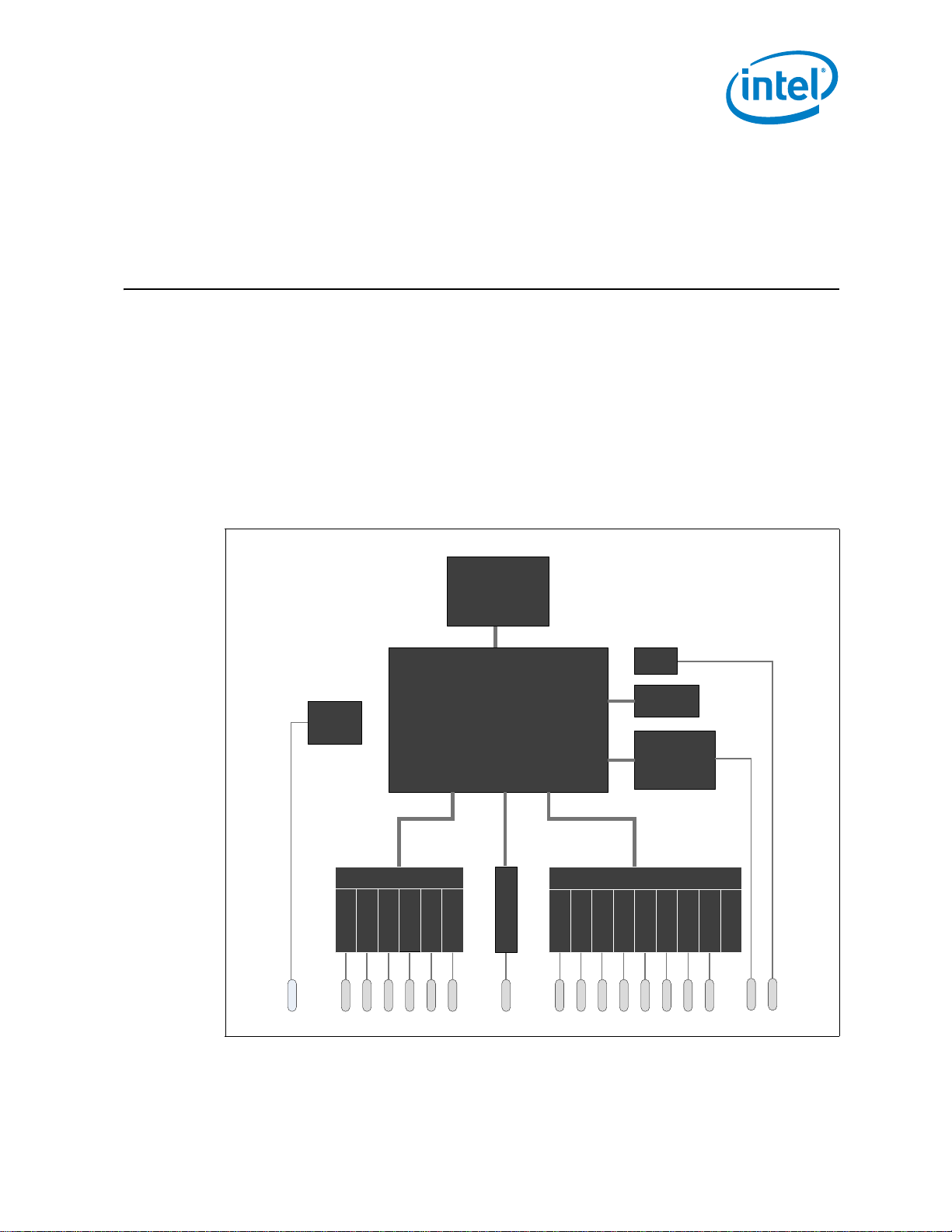
®
,QWHO4XDUN
&RUH
+RVW%ULGJH
&ORFN
H65$0
''5
0HPRU\
&RQWUROOHU
-7$*
/HJDF\%ULGJH
$0%$)DEULF
30&
*3,2
57&
+3(7
$3,&
63,
520
6',2
8$57
86%
,
&*3,2
3&,H
,2
,2
,2
,2
,2
,2
,2
,2
,2
,2
,2
,2
,2
,2
,2
,2
,2
(7+
,2
63,
Intel
Quark SoC X1000 Core Overview—Intel® Quark Core
2.0 Intel® Quark SoC X1000 Core Overview
The Intel® Quark Core enables a range of low-cost, high-performance embedded
system designs capable of running applications written for the Intel architecture. The
Intel® Quark Core integrates a 16-Kbyte unified cache and floating-point hardware onchip for improved performance. For further details, including the Intel
feature list, see Chapter 2 in the Intel
Manual.
2.1 Intel® Quark Core Architecture
Figure 1 shows how the Intel® Quark Core is implemented in the Intel® Quark SoC
X1000.
Figure 1. Intel® Quark SoC X1000 Core used in Intel® Quark SoC X1000
®
Quark SoC X1000 Core Hardware Reference
®
Quark Core
October 2013 Developer’s Manual
Order Number: 329679-001US 21
Intel® Quark SoC X1000 Core
Page 22

3.0 Architectural Overview
3.1 Internal Architecture
Intel® Quark Core—Architectural Overview
The Intel® Quark Core has a 32-bit architecture with on-chip memory management
and cache and floating-point units. The Intel
sizing for the external data bus; that is, the bus size can be specified as 8-, 16-, or 32bits wide.
Note: The implementation of Intel
®
dynamic bus sizing. Bus width is fixed at 32 bits.
®
Intel
Quark Core functional units are listed below:
• Bus Interface Unit (BIU)
•Cache Unit
• Instruction Prefetch Unit
• Instruction Decode Unit
• Control Unit
• Integer (Datapath) Unit
• Floating-Point Unit
• Segmentation Unit
• Paging Unit
For further details, see Chapter 3 in the Intel
Reference Manual.
3.2 System Architecture
®
Quark Core also supports dynamic bus
Quark Core on Intel® Quark SoC X1000 does not support
®
Quark SoC X1000 Core Hardware
Intel® Quark Core System Architecture includes the following:
• Memory Organization
• I/O Space
• Addressing Modes
• Data Types
• Interrupts
3.3 Memory Organization
Memory on the Intel® Quark SoC X1000 Core is divided up into 8-bit quantities (bytes),
16-bit quantities (words), and 32-bit quantities (dwords). Words are stored in two
consecutive bytes in memory with the low-order byte at the lowest address, the high
order byte at the high address. Dwords are stored in four consecutive bytes in memory
with the low-order byte at the lowest address, the high-order byte at the highest
address. The address of a word or dword is the byte address of the low-order byte.
®
Quark SoC X1000 Core
Intel
Developer’s Manual October 2013
22 Order Number: 329679-001US
Page 23

Architectural Overview—Intel
®
Quark Core
In addition to these basic data types, the Intel® Quark SoC X1000 Core supports two
larger units of memory: pages and segments. Memory can be divided up into one or
more variable-length segments, which can be swapped to disk or shared between
programs. Memory can also be organized into one or more 4-Kbyte pages. Both
segmentation and paging can be combined, gaining the advantages of both systems.
The Intel
®
Quark SoC X1000 Core supports both pages and segments in order to
provide maximum flexibility to the system designer. Segmentation and paging are
complementary. Segmentation is useful for organizing memory in logical modules, and
as such is a tool for the application programmer, while pages are useful for the system
programmer for managing the physical memory of a system.
3.3.1 Address Spaces
The Intel® Quark SoC X1000 Core has three distinct address spaces: logical, linear , and
physical. A logical address (also known as a virtual address) consists of a selector and
an offset. A selector is the contents of a segment register. An offset is formed by
summing all of the addressing components (BASE, INDEX, DISPLACEMENT) discussed
in Section 3.5.3 into an effective address. Because each task on the Intel® Quark SoC
X1000 Core has a maximum of 16 K (2
32
(2
bits), this gives a total of 246 bits or 64 terabytes of logical address space per task.
The programmer sees this virtual address space.
The segmentation unit translates the logical address space into a 32-bit linear address
space. If the paging unit is not enabled then the 32-bit linear address corresponds to
the physical address. The paging unit translates the linear address space into the
physical address space. The physical address is what appears on the address pins.
14
- 1) selectors, and offsets can be 4 Gbytes
The primary difference between Real Mode and Protected Mode is how the
segmentation unit performs the translation of the logical address into the linear
address. In Real Mode, the segmentation unit shifts the selector left four bits and adds
the result to the offset to form the linear address. While in Protected Mode every
selector has a linear base address associated with it. The linear base address is stored
in one of two operating system tables (i.e., the Local Descriptor Table or Global
Descriptor Table). The selector's linear base address is added to the offset to form the
final linear address.
Figure 2 shows the relationship between the various address spaces.
October 2013 Developer’s Manual
Order Number: 329679-001US 23
Intel® Quark SoC X1000 Core
Page 24
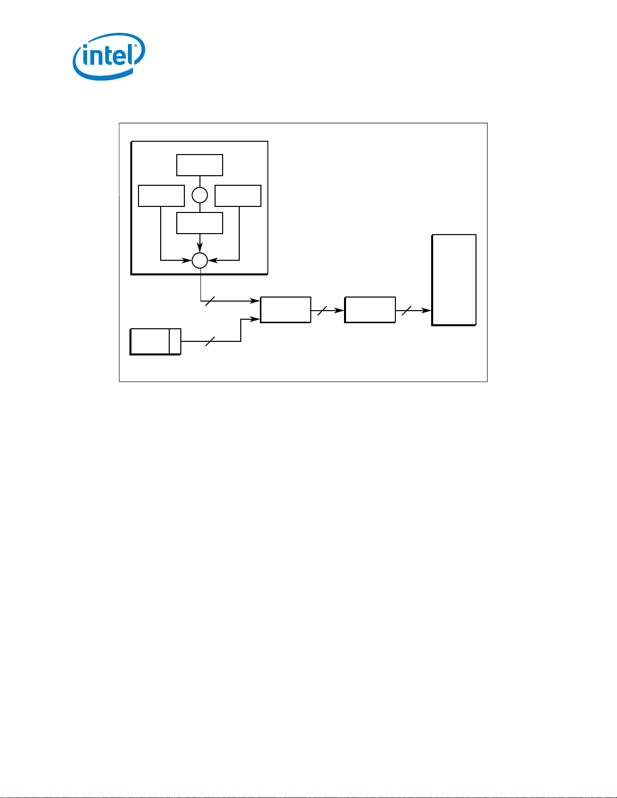
Figure 2. Address Translation
A5158-01
Effective
Address
32
Physical
Address
32
32
Segmentation
Unit
Selector
R
P
L
Logical or
Virtual Address
13
Descriptor Index
03215
Segment Register
Linear
Address
Paging Unit
(optional use)
Physical
Memory
BE3#–BE0#
A31–A2
031
Effective Address Calculation
Displacement
Index
Base
Scale
1, 2, 3, 4
X
+
Intel® Quark Core—Architectural Overview
3.3.2 Segment Register Usage
The main data structure used to organize memory is the segment. On the Intel® Quark
SoC X1000 Core, segments are variable sized blocks of linear addresses which have
certain attributes associated with them. There are two main types of segments: code
and data. The segments are of variable size and can be as small as 1 byte or as large
as 4 Gbytes (2
In order to provide compact instruction encoding, and increase Intel
32
bytes).
®
Quark SoC
X1000 Core performance, instructions do not need to explicitly specify which segment
register is used. A default segment register is automatically chosen according to the
rules of Table 3. In general, data references use the selector contained in the DS
register; stack references use the SS register and Instruction fetches use the CS
register. The contents of the Instruction Pointer provide the offset. Special segment
override prefixes allow the explicit use of a given segment register, and override the
implicit rules listed in Table 3. The override prefixes also allow the use of the ES, FS and
GS segment registers.
There are no restrictions regarding the overlapping of the base addresses of any
segments. Thus, all 6 segments could have the base address set to zero and create a
system with a 4-Gbyte linear address space. This creates a system where the virtual
address space is the same as the linear address space. Further details of segmentation
are discussed in Chapter 6.0, “Protected Mode Architecture.”
®
Quark SoC X1000 Core
Intel
Developer’s Manual October 2013
24 Order Number: 329679-001US
Page 25
Architectural Overview—Intel
®
Quark Core
3.4 I/O Space
The Intel® Quark SoC X1000 Core allows 64 K+3 bytes to be addressed within the I/O
space. The Host Bridge propagates the Intel
without any translation on to the destination bus and, therefore, provides
addressability for 64 K+3 byte locations. Note that the upper three locations can be
accessed only during I/O address wrap-around when processor bus A16# address
signal is asserted. A16# is asserted on the processor bus when an I/O access is made
to 4 bytes from address 0FFFDh, 0FFFEh, or 0FFFFh. A16# is also asserted when an I/O
access is made to 2 bytes from address 0FFFFh.
Table 3. Segment Register Selection Rules
Type of Memory Reference
Code Fetch CS None
Destination of PUSH, PUSHF, INT, CALL, PUSHA
Instructions
Source of POP, POPA, POPF, IRET, RET instructions SS None
Destination of STOS, MOVS, REP STOS, REP MOVS
Instructions (DI is Base Register)
Other Data References, with Effective Address using
Base Register of:
[EAX] DS
[EBX] DS
[ECX] DS
[EDX] DS All
[ESI] DS
[EDI] DS
[EBP] SS
[ESP] SS
®
Quark SoC X1000 Core I/O address
Implied (Default)
Segment Use
SS None
ES None
Segment Override
Prefixes Possible
The I/O ports are accessed via the IN and OUT I/O instructions, with the port address
supplied as an immediate 8-bit constant in the instruction or in the DX register. All 8and 16-bit port addresses are zero extended on the upper address lines. The I/O
instructions cause the M/IO# pin to be driven low.
I/O port addresses 00F8H through 00FFH are reserved for use by Intel.
I/O instruction code is cacheable.
I/O data is not cacheable.
I/O transfers (data or code) can be bursted.
3.5 Addressing Modes
3.5.1 Addressing Modes Overview
The Intel® Quark SoC X1000 Core provides a total of 11 addressing modes for
instructions to specify operands. The addressing modes are optimized to allow the
efficient execution of high-level languages such as C and FOR TRAN, and they co ver the
vast majority of data references needed by high-level languages.
October 2013 Developer’s Manual
Order Number: 329679-001US 25
Intel® Quark SoC X1000 Core
Page 26

3.5.2 Register and Immediate Modes
The following two addressing modes provide for instructions that operate on register or
immediate operands:
• Register Operand Mode: The operand is located in one of the 8-, 16- or 32-bit
general registers.
• Immediate Operand Mode: The operand is included in the instruction as part of the
opcode.
3.5.3 32-Bit Memory Addressing Modes
The remaining modes provide a mechanism for specifying the effective address of an
operand. The linear address consists of two components: the segment base address
and an effective address. The effective address is calculated by using combinations of
the following four address elements:
• DISPLACEMENT: An 8-, or 32-bit immediate value, following the instruction.
• BASE: The contents of any general purpose register. The base registers are
generally used by compilers to point to the start of the local variable area.
• INDEX: The contents of any general purpose register except for ESP. The index
registers are used to access the elements of an array, or a string of characters.
• SCALE: The index register's value can be multiplied by a scale factor, either 1, 2, 4
or 8. Scaled index mode is especially useful for accessing arrays or structures.
Intel® Quark Core—Architectural Overview
Combinations of these 4 components make up the 9 additional addressing modes.
There is no performance penalty for using any of these addressing combinations,
because the effective address calculation is pipelined with the execution of other
instructions. The one exception is the simultaneous use of Base and Index components,
which requires one additional clock.
As shown in Figure 3, the effective address (EA) of an operand is calculated according
to the following formula:
EA = Base Reg + (Index Reg * Scaling) + Displacement
Direct Mode: The operand’s offset is contained as part of the instruction as an 8-, 16or 32-bit displacement.
Example: INC Word PTR [500]
Register Indirect Mode: A BASE register contains the address of the operand.
Example: MOV [ECX], EDX
Based Mode: A BASE register's contents is added to a DISPLACEMENT to form the
operand's offset.
Example: MOV ECX, [EAX+24]
Index Mode: An INDEX register’s contents is added to a DISPLACEMENT to form the
operand's offset.
Example: ADD EAX, TABLE[ESI]
Scaled Index Mode: An INDEX register's contents is multiplied by a scaling factor
which is added to a DISPLACEMENT to form the operand's offset.
Example: IMUL EBX, TABLE[ESI*4],7
Based Index Mode: The contents of a BASE register is added to the contents of an
INDEX register to form the effective address of an operand.
Example: MOV EAX, [ESI] [EBX]
®
Quark SoC X1000 Core
Intel
Developer’s Manual October 2013
26 Order Number: 329679-001US
Page 27
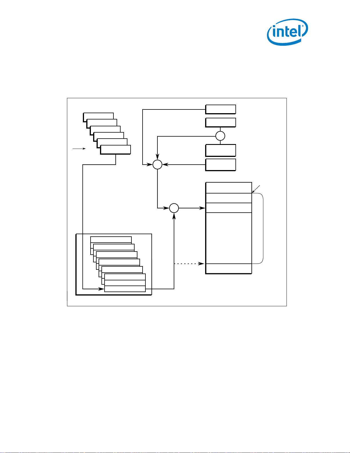
Architectural Overview—Intel
A5159-01
Segment Register
Descriptor Register
Linear
Address
Selector
Index Register
Base Register
X
SS
SelectorGS
SelectorFS
SelectorES
SelectorDS
SelectorCS
+
Segment Base Address
Target Address
Displacement
(in instruction)
Scale
1, 2, 4, or 8
+
Effective
Address
Selected
Segment
Selected
Limit
Access Rights SS
Access Rights GS
Access Rights FS
Access Rights ES
Access Rights DS
Limits
Access Rights CS
Base Address
®
Quark Core
Based Scaled Index Mode: The contents of an INDEX register is multiplied by a
SCALING factor and the result is added to the contents of a BASE register to obtain the
operand's offset.
Example: MOV ECX, [EDX*8] [EAX]
Figure 3. Addressing Mode Calculations
October 2013 Developer’s Manual
Order Number: 329679-001US 27
Based Index Mode with Displacement: The contents of an INDEX Register and a
BASE register's contents and a DISPLACEMENT are all summed together to form the
operand offset.
Example: ADD EDX, [ESI] [EBP+00FFFFF0H]
Based Scaled Index Mode with Displacement: The contents of an INDEX register
are multiplied by a SCALING factor, the result is added to the contents of a BASE
register and a DISPLACEMENT to form the operand’s offset.
Example: MOV EAX, LOCALTABLE[EDI*4] [EBP+80]
Intel® Quark SoC X1000 Core
Page 28
Intel® Quark Core—Architectural Overview
3.5.4 Differences Between 16- and 32-Bit Addresses
In order to provide software compatibility with older processors, the Intel® Quark SoC
X1000 Core can execute 16-bit instructions in Real and Protected Modes. The processor
determines the size of the instructions it is executing by examining the D bit in the CS
segment Descriptor. If the D bit is 0 then all operand lengths and effective addresses
are assumed to be 16 bits long. If the D bit is 1 then the default length for operands
and addresses is 32 bits. In Real Mode the default size for operands and addresses is
16-bits.
Regardless of the default precision of the operands or addresses, the Intel
X1000 Core is able to execute either 16- or 32-bit instructions. This is specified via the
use of override prefixes. Two prefixes, the Operand Size Prefix and the Address Length
Prefix, override the value of the D bit on an individual instruction basis. These prefixes
are automatically added by Intel assemblers.
Example: The Intel
programmer needs to access the EAX registers. The assembler code for this might be
MOV EAX, 32-bit MEMORY OP. The Macro Assembler automatically determines that an
Operand Size Prefix is needed and generates it.
Example: The D bit is 0, and the programmer wishes to use Scaled Index addressing
mode to access an array. The Address Length Prefix allows the use of MOV DX,
TABLE[ESI*2]. The assembler uses an Address Length Prefix because, with D=0, the
default addressing mode is 16-bits.
®
Quark SoC X1000 Core is executing in Real Mode and the
®
Quark SoC
Example: The D bit is 1, and the program wants to store a 16-bit quantity . The Operand
Length Prefix is used to specify only a 16-bit value; MOV MEM16, DX.
The OPERAND LENGTH and Address Length Prefixes can be applied separately or in
combination to any instruction. The Address Length Prefix does not allow addresses
over 64 Kbytes to be accessed in Real Mode. A memory address which exceeds FFFFH
will result in a General Protection Fault. An Address Length Prefix only allows the use of
the additional Intel
When executing 32-bit code, the Intel
®
Quark SoC X1000 Core addressing modes.
®
Quark SoC X1000 Core uses either 8-, or 32-bit
displacements, and any register can be used as base or index registers. When
executing 16-bit code, the displacements are either 8, or 16 bits, and the base and
index register are as listed in Table 4 below.
Table 4. BASE and INDEX Registers for 16- and 32-Bit Addresses
16-Bit Addressing 32-Bit Addressing
BASE REGISTER BX,BP Any 32-bit GP Register
INDEX REGISTER SI,DI Any 32-bit GP Register Except ESP
SCALE FACTOR none 1, 2, 4, 8
DISPLACEMENT 0, 8, 16 bits 0, 8, 32 bits
3.6 Data Types
3.6.1 Data Types
The Intel® Quark SoC X1000 Core can support a wide-variety of data types. In the
following descriptions, the processor consists of the base architecture registers.
®
Quark SoC X1000 Core
Intel
Developer’s Manual October 2013
28 Order Number: 329679-001US
Page 29
Architectural Overview—Intel
07
8 bits10
2
X8-Bit Integer
0
31
32 bits0–4GXDword
015
16 bits0–64KXWord
07
07
07
07
07
07
07
07
07077
07
8 bits0–255XByte
PrecisionRangeData Format
Two's
Complement
Sign Bit
015
16 bits10
4
XX16-Bit Integer
Two's
Complement
07
2 Digits0–9X8-Bit Packed BCD
07
1 Digit0–9X8-Bit Unpacked BCD
0
63
64 bits10
19
X64-Bit Integer
0
31
32 bits10
9
X32-Bit Integer
Two BCD Digits per Byte
One BCD Digit per Byte
6379
Sign Bit
Biased Exp.
0
7279
18 Digits±10
±18
X80-Bit Packed BCD
Sign Bit
53 bits±10
±308
XDouble Precision Real
31
23
Biased ExpBiased Exp
0
Significand
Significand
0
24 bits±10
±38
XSingle Precision Real
0
64 bits±10
±4932
XExtended Precision Real
X
Two's
Complement
Two's
Complement
Ignored
63
52
Biased Exp
Supported by FPU
Supported by Base Registers
Least Significant Byte
Sign Bit
Sign Bit
Sign Bit
Sign Bit
Sign Bit
Figure 4. Data Types
®
Quark Core
3.6.1.1 Unsigned Data Types
Byte: Unsigned 8-bit quantity
Word: Unsigned 16-bit quantity
Dword: Unsigned 32-bit quantity
3.6.1.2 Signed Data Types
The least significant bit (LSB) in a byte is bit 0, and the most significant bit is 7.
All signed data types assume 2's complement notation. The signed data types contain
two fields, a sign bit and a magnitude. The sign bit is the most significant bit (MSB).
The number is negative if the sign bit is 1. If the sign bit is 0, the number is positive.
The magnitude field consists of the remaining bits in the number. (Refer to Figure 5.)
October 2013 Developer’s Manual
Order Number: 329679-001US 29
Intel® Quark SoC X1000 Core
Page 30

8-bit Integer: Signed 8-bit quantity
16-bit Integer: Signed 16-bit quantity
32-bit Integer: Signed 32-bit quantity
64-bit Integer: Signed 64-bit quantity
The integer core of the Intel
®
Quark SoC X1000 Core only support 8-, 16- and 32-bit
integers. See Section 3.6.1.4 for details.
3.6.1.3 BCD Data Types
The Intel® Quark SoC X1000 Core supports packed and unpacked binary coded decimal
(BCD) data types. A packed BCD data type contains two digits per byte, the lower digit
is in bits 3:0 and the upper digit in bits 7:4. An unpacked BCD data type contains 1
digit per byte stored in bits 3:0.
The Intel® Quark SoC X1000 Core supports 8-bit packed and unpacked BCD data
types. (Refer to Figure 5.)
3.6.1.4 Floating-Point Data Types
In addition to the base registers, the Intel® Quark SoC X1000 Core on-chip floatingpoint unit consists of the floating-point registers. The floating-point unit data type
contain three fields: sign, significand, and exponent. The sign field is one bit and is the
MSB of the floating-point number. The number is negative if the sign bit is 1. If the sign
bit is 0, the number is positive. The significand gives the significant bits of the number.
The exponent field contains the power of 2 needed to scale the significand, see
Figure 5.
Intel® Quark Core—Architectural Overview
Only the FPU supports floating-point data types.
Single Precision Real: 23-bit significand and 8-bit exponent. 32 bits total.
Double Precision Real: 52-bit significand and 11-bit exponent. 64 bits total.
Extended Precision Real: 64-bit significand and 15-bit exponent. 80 bits total.
Floating-Point Unsigned Data Types
The on-chip FPU does not support unsigned data types. (Refer to Figure 5.)
Floating-Point Signed Data Types
The on-chip FPU only supports 16-, 32- and 64-bit integers.
Floating-Point BCD Data Types
The on-chip FPU only supports 80-bit packed BCD data types.
3.6.1.5 String Data Types
A string data type is a contiguous sequence of bits, bytes, words or dwords. A string
may contain between 1 byte and 4 Gbytes. (Refer to Figure 6.)
String data types are only supported by the CPU section of the Intel
Core.
Byte String: Contiguous sequence of bytes.
Word String: Contiguous sequence of words.
Dword String: Contiguous sequence of dwords.
Bit String: A set of contiguous bits. In the Intel
strings can be up to 4-gigabits long.
®
Quark SoC X1000
®
Quark SoC X1000 Core bit
®
Quark SoC X1000 Core
Intel
Developer’s Manual October 2013
30 Order Number: 329679-001US
Page 31

Architectural Overview—Intel
07
8 bits10
2
X8-Bit Integer
0
31
32 bits0–4GXDword
015
16 bits0–64KXWord
07
07
07
07
07
07
07
0707077
07
8 bits0–255XByte
PrecisionRangeData Format
Two's
Complement
Sign Bit
015
16 bits10
4
XX16-Bit Integer
Two's
Complement
07
2 Digits0–9X8-Bit Packed BCD
07
1 Digit0–9X8-Bit Unpacked BCD
0
63
64 bits10
19
X64-Bit Integer
031
32 bits10
9
X32-Bit Integer
Two BCD Digits per Byte
One BCD Digit per Byte
6379
Sign Bit
Biased Exp.
0
7279
18 Digits±10
±18
X80-Bit Packed BCD
Sign Bit
53 bits±10
±308
XDouble Precision Real
31
23
Biased ExpBiased Exp
0
Significand
Significand
0
24 bits±10
±38
XSingle Precision Real
0
64 bits±10
±4932
XExtended Precision Real
X
Two's
Complement
Two's
Complement
Ignored
63
52
Biased Exp
Supported by FPU
Supported by Base Registers
Least Significant Byte
Sign Bit
Sign Bit
Sign Bit
Sign Bit
Sign Bit
®
Quark Core
3.6.1.6 ASCII Data Types
The Intel® Quark SoC X1000 Core supports ASCII (American Standard Code for
Information Interchange) strings and can perform arithmetic operations (such as
addition and division) on ASCII data. The Intel
operate on ASCII data; see Figure 6.
Figure 5. Data Types
®
Quark SoC X1000 Core can only
October 2013 Developer’s Manual
Order Number: 329679-001US 31
Intel® Quark SoC X1000 Core
Page 32

Figure 6. String and ASCII Data Types
A5161-01
7
Bit
String
+2,147,483,647
0
7
0
7
0
7
0
A+268,435,455
A+3
A+2
7
07..1 0
A+1
A
+7
+1 0
7
0
A-1
7
07..1 0
A-2
A-3
7
0
7
0
-2,147,483,647
A-268,435,455
Dword
String
. . . .
31
0
A+4N
A+4N+2A+4N+3 A+4N+1
31
0
A+4
A+6A+7 A+5
31
0
A
A+2A+3 A+1
01N
15
A+2N-1 A+2N
0
15
0
A
A+2A+3 A+1
01
150
N
. . . .
Word
String
7
A+N
0
7
0
A
A+1
01
70
N
. . . .
Byte
String
Address
String Data Types
ASCII Data Types
7
0
ASCII
Character
A5162-01
Data Format
Least Significant Byte
31
047
OffsetSelector48-bit Pointer
31
0
Offset32-bit Pointer
Intel® Quark Core—Architectural Overview
Figure 7. Pointer Data Types
3.6.1.7 Pointer Data Types
A pointer data type contains a value that gives the address of a piece of data. Intel®
Quark SoC X1000 Core support the following two types of pointers (see Figure 7):
®
Intel
Developer’s Manual October 2013
32 Order Number: 329679-001US
• 48-bit Pointer: 16-bit selector and 32-bit offset
• 32-bit Pointer: 32-bit offset
Quark SoC X1000 Core
Page 33

Architectural Overview—Intel
A5163-01
0
87
Dword in Little-Endian Memory Format
16 1524 2331
m + 3
m + 2
m + 1
m
0
87
Dword in Big-Endian Memory Format
16 1524 2331
m
m + 1
m + 2
m + 3
®
Quark Core
3.6.2 Little Endian vs. Big Endian Data Formats
The Intel® Quark SoC X1000 Core, as well as all other members of the Intel
architecture, use the “little-endian” method for storing data types that are larger than
one byte. Words are stored in two consecutive bytes in memory with the low-order byte
at the lowest address and the high order byte at the high address. Dwords are stored in
four consecutive bytes in memory with the low-order byte at the lowest address and
the high order byte at the highest address. The address of a word or dword data item is
the byte address of the low-order byte.
Figure 8 illustrates the differences between the big-endian and little-endian formats for
dwords. The 32 bits of data are shown with the low order bit numbered bit 0 and the
high order bit numbered 32. Big-endian data is stored with the high-order bits at the
lowest addressed byte. Little-endian data is stored with the high-order bits in the
highest addressed byte.
The Intel
16- or 32-bit data between the two byte orderings:
• BSWAP (byte swap) handles 4-byte values
• XCHG (exchange) handles 2-byte values
Figure 8. Big vs. Little Endian Memory Format
®
Quark SoC X1000 Core has the following two instructions that can convert
3.7 Interrupts
3.7.1 Interrupts and Exceptions
Interrupts and exceptions alter the normal program flow, in order to handle external
events, to report errors or exceptional conditions. The difference between interrupts
and exceptions is that interrupts are used to handle asynchronous external events
while exceptions handle instruction faults. Although a program can generate a software
interrupt via an INT N instruction, the Intel
interrupts as exceptions.
Hardware interrupts occur as the result of an external event and are classified into two
types: maskable or non-maskable. Interrupts are serviced after the execution of th e
current instruction. After the interrupt handler is finished servicing the interrupt,
execution proceeds with the instruction immediately after the interrupted instruction.
Section 3.7.3 and Section 3.7.4 discuss the differences between Maskable and Non-
Maskable interrupts.
October 2013 Developer’s Manual
Order Number: 329679-001US 33
®
Quark SoC X1000 Core treats software
Intel® Quark SoC X1000 Core
Page 34

Intel® Quark Core—Architectural Overview
Exceptions are classified as faults, traps, or aborts, depending on the way they are
reported, and whether or not restart of the instruction causing the exception is
supported. Faults are exceptions that are detected and serviced before the execution
of the faulting instruction. A fault would occur in a virtual memory system when the
processor referenced a page or a segment that was not present. The operating system
would fetch the page or segment from disk, and then the Intel
®
Quark Core would
restart the instruction. Traps are exceptions that are reported immediately after the
execution of the instruction that caused the problem. User defined interrupts are
examples of traps. Aborts are exceptions that do not permit the precise location of the
instruction causing the exception to be determined. Aborts are used to report severe
errors, such as a hardware error or illegal values in system tables.
Thus, when an interrupt service routine has been completed, execution proceeds from
the instruction immediately following the interrupted instruction. On the other hand,
the return address from an exception fault routine will always point at the instruction
causing the exception and include any leading instruction prefixes. Table 5 and Table 6
summarize the possible interrupts for Intel
®
Quark SoC X1000 Core and shows where
the return address points.
®
Intel
Quark SoC X1000 Core can handle up to 256 different interrupts and/or
exceptions. In order to service the interrupts, a table with up to 256 interrupt vectors
must be defined. The interrupt vectors are simply pointers to the appropriate interrupt
service routine. In Real Mode (see Chapter 5.0, “Real Mode Architecture”), the vectors
are 4-byte quantities, a Code Segment plus a 16-bit offset; in Protected Mode, the
interrupt vectors are 8-byte quantities, which are put in an Interrupt Descriptor Table
(see Section 6.2.3.4, “Interrupt Descriptor Table” on page 71). Of the 256 possible
interrupts, 32 are reserved for use by Intel, the remaining 224 are free to be used by
the system designer.
3.7.2 Interrupt Processing
When an interrupt occurs, the following actions happen. First, the current program
address and the Flags are saved on the stack to allow resumption of the interrupted
program. Next, an 8-bit vector is supplied to the Intel
appropriate entry in the interrupt table. The table contains the starting address of the
interrupt service routine. Then, the user supplied interrupt service routine is executed.
Finally, when an IRET instruction is executed the old Intel
restored and program execution resumes at the appropriate instruction.
The 8-bit interrupt vector is supplied to the Intel
ways: exceptions supply the interrupt vector internally; software INT instructions
contain or imply the vector; maskable hardware interrupts supply the 8-bit vector via
the interrupt acknowledge bus sequence. Non-maskable hardware interrupts are
assigned to interrupt vector 2.
3.7.3 Maskable Interrupt
Maskable interrupts are the most common way used by the Intel® Quark Core to
respond to asynchronous external hardware events. A hardware interrupt occurs when
the INTR is pulled high and the Interrupt Flag bit (IF) is enabled. The Intel
only responds to interrupts between instructions, (REPeat String instructions, have an
“interrupt window,” between memory moves, which allows interrupts during long string
moves). When an interrupt occurs, the Intel
supplied by the hardware which identifies the source of the interrupt, (one of 224 user
defined interrupts). The exact nature of the interrupt sequence is discussed in Section
10.3.10, “Interrupt Acknowledge” on page 219.
®
Quark Core which identifies the
®
Quark Core state is
®
Quark Core in several different
®
Quark Core
®
Quark Core reads an 8-bit vector
®
Quark SoC X1000 Core
Intel
Developer’s Manual October 2013
34 Order Number: 329679-001US
Page 35

Architectural Overview—Intel
®
Quark Core
The IF bit in the EFLAG registers is reset when an interrupt is being serviced. This
effectively disables servicing additional interrupts during an interrupt service routine.
However, the IF may be set explicitly by the interrupt handler, to allow the nesting of
interrupts. When an IRET instruction is executed, the original state of the IF is restored.
Table 5. Interrupt Vector Assignments
Function
Divide Error 0 DIV, IDIV YES FAULT
Debug Exception 1 Any instruction YES TRAP†
NMI Interrupt 2 INT 2 or NMI NO NMI
One Byte Interrupt 3 INT NO TRAP
Interrupt on Overflow 4 INTO NO TRAP
Array Bounds Check 5 BOUND YES FAULT
Invalid OP-Code 6 Any illegal instruction YES FAULT
Device Not Available 7 ESC, WAIT YES FAULT
Double Fault 8
Intel Reserved 9
Invalid TSS 10 JMP, CALL, IRET, INT YES FAULT
Segment Not Present 11 Segment Register Instr uctions YES FAULT
Stack Fault 12 Stack References YES FAULT
General Protection Fault 13 Any Memory Reference YES FAULT
Page Fault 14
Intel Reserved 15
Alignment Check Interrupt 17 Unaligned Memory Access YES FAULT
Intel Reserved 18–31
Two Byte Interrupt 0–255 INT n NO TRAP
†Some debug exceptions may report both traps on the previous instructio n, and faults on the next instructio n.
Interrupt
Number
Instruction that can cause
Any instruction that can
generate an exception
Any Memory Access or Code
Fetch
exception
Return Address
Points to Faulting
Instruction
YES FAULT
Type
ABORT
Table 6. FPU Interrupt Vector Assignments
Function
Floating-Point Error 16 Floating-point, WAIT YES FAULT
Interrupt
Number
Instruction that can
cause exception
Return Address Points to
Faulting Instruction
Type
3.7.4 Non-Maskable Interrupt
Non-maskable interrupts provide a method of servicing very high priority interrupts. A
common example of the use of a non-maskable interrupt (NMI) would be to activate a
power failure routine or SMI# to activate a power saving mode. When the NMI input is
pulled high, it causes an interrupt with an internally supplied vector value of 2. Unlike a
normal hardware interrupt, no interrupt acknowledgment sequence is performed for an
NMI.
October 2013 Developer’s Manual
Order Number: 329679-001US 35
Intel® Quark SoC X1000 Core
Page 36

While executing the NMI s ervicing procedure, the Intel® Quark Core will not service
further NMI requests until an interrupt return (IRET) instruction is executed or the
processor is reset (RSM in the case of SMI#). If NMI occurs while currently servicing an
NMI, its presence will be saved for servicing after executing the first IRET instruction.
The IF bit is cleared at the beginning of an NMI interrupt to inhibit further INTR
interrupts.
3.7.5 Software Interrupts
A third type of interrupt/exception for the Intel® Quark Core is the software interrupt.
An INT n instruction causes the processor to execute the interrupt service routine
pointed to by the nth vector in the interrupt table.
A special case of the two byte software interrupt INT n is the one byte INT 3, or
breakpoint interrupt. By inserting this one byte instruction in a program, you can set
breakpoints in your program as a debugging tool.
A final type of software interrupt is the single step interrupt. It is discussed in Section
11.2, “Single-Step Trap” on page 246.
3.7.6 Interrupt and Exception Priorities
Interrupts are externally-generated events. Maskable Interrupts (on the INTR input)
and Non-Maskable Interrupts (on the NMI input or SMI# input) are recognized at
instruction boundaries. When more than one interrupt or external event are both
recognized at the same instruction boundary, the Intel
highest priority routine first. (See list below.) If , after the NMI service routine has been
invoked, maskable interrupts are still enabled, then the Intel® Quark SoC X1000 Core
will invoke the appropriate interrupt service routine.
Priority for Servicing External Events for Intel
1. RESET/SRESET
2. FLUSH#
3. SMI#
4. NMI
5. INTR
6. STPCLK#
Intel® Quark Core—Architectural Overview
®
Quark Core invokes the
®
Quark SoC X1000 Core:
Note: STPCLK# will be recognized while in an interrupt service routine or an SMM handler.
®
Exceptions are internally-gen erated events. Exceptions are detect ed by the Intel
Quark SoC X1000 Core if, in the course of executing an instruction, the Intel
SoC X1000 Core detects a problematic condition. The Intel
then immediately invokes the appropriate exception service routine. The state of the
®
Intel
Quark SoC X1000 Core is such that the instruction causing the exception can be
®
Quark SoC X1000 Core
®
Quark
restarted. If the exception service routine has taken care of the problematic condition,
the instruction will execute without causing the same exception.
It is possible for a single instruction to generate several exceptions (for example,
transferring a single operand could generate two page faults if the operand location
spans two “not present” pages). However, only one exception is generated upon each
attempt to execute the instruction. Each exception service routine should correct its
corresponding exception, and restart the instruction. In this manner, exceptions are
serviced until the instruction executes successfully.
®
Quark SoC X1000 Core
Intel
Developer’s Manual October 2013
36 Order Number: 329679-001US
Page 37

Architectural Overview—Intel
®
Quark Core
As the Intel® Quark SoC X1000 Core executes instructions, it follows a consistent cycle
in checking for exceptions. Consider the case of the Intel
having just completed an instruction. It then performs the checks listed in Table 7
before reaching the point where the next instruction is completed. This cycle is
repeated as each instruction is executed, and occurs in parallel with instruction
decoding and execution. Checking for EM, TS, or FPU error status only occurs for
processors with on-chip Floating-Point Units.
Table 7. Sequence of Exception Checking
Sequence Description
Check for Exception 1 T r aps from the inst ruction just completed (single-step via Trap Flag, or
1
Data Breakpoints set in the Debug Registers).
Check for Exception 1 Faults in the next instruction (Instruction Execution Breakpoint set in
2
the Debug Registers for the ne xt instruction).
3 Check for external NMI and INTR.
Check for Segmentation Faults that prevented fetching the entire next instruction
4
(exceptions 11 or 13).
5 Check for Page Faults that prevented fetching the entire next instruction (exception 14).
Check for Faults decoding the next instruction (exception 6 if illegal opcode; ex ception 6 if in
Real Mode or in Virtual 8086 Mode and attempting to execute an instruction for Protected
6
Mode only (see Section 6.5.4, “Protection and I/O Permission Bitmap” on page 109); or
exception 13 if instruction is longer than 15 bytes, or privilege violation in Protected Mode
(i.e., not at IOPL or at CPL=0).
7 If WAIT opcode, check if TS=1 and MP=1 (exception 7 if both are 1).
8 If opcode for Floating-Point Unit, check if EM=1 or TS=1 (exception 7 if either are 1).
If opcode for Floating-Point Unit (FPU), check FPU error status (exception 16 if error status is
9
asserted).
Check in the following order for each memory reference required by the instruction:
10
Note: The order stated supports the concept of the paging mechanism being “underneath” the
a. Check for Segmentation Faults that prevent transferring the entire memory quantity
(exceptions 11, 12, 13).
b. Check for Page Faults that prevent transferring the entire memory quantity (exception
14).
segmentation mechanism. Therefore, for any given code or data reference in memory,
segmentation exceptions are generated before paging exceptions are generated.
®
Quark SoC X1000 Core
3.7.7 Instruction Restart
The Intel® Quark SoC X1000 Core fully supports restarting all instructions after faults.
If an exception is detected in the instruction to be executed (exception categories 4
through 10 in Table 8), the Intel® Quark SoC X1000 Core invokes the appropriate
exception service routine.
The Intel
for all cases except the following. An instruction causes a task switch to a task whose
Task State Segment is partially “not present.” (An entirely “not present” TSS is
restartable.) Partially present TSSs can be avoided either by keeping the TSSs of such
tasks present in memory , or by aligning TS S segments to reside entirely within a single
4 K page (for TSS segments of 4 Kbytes or less).
Note: Partially present task state segments can be easily avoided by proper design of the
operating system.
October 2013 Developer’s Manual
Order Number: 329679-001US 37
®
Quark SoC X1000 Core is in a state that permits restart of the instruction,
Intel® Quark SoC X1000 Core
Page 38

3.7.8 Double Fault
A Double Fault (exception 8) results when the Intel® Quark SoC X1000 Core attempts
to invoke an exception service routine for the segment exceptions (10, 11, 12 or 13),
but in the process of doing so, detects an exception other than a Page Fault (exception
14).
A Double Fault (exception 8) will also be generated when the Intel
Core attempts to invoke the Page Fault (exception 14) service routine, and detects an
exception other than a second Page Fault. In any functional system, the entire Page
Fault service routine must remain “present” in memory.
When a Double Fault occurs, the Intel
®
Quark SoC X1000 Core invokes the exception
service routine for exception 8.
3.7.9 Floating-Point Interrupt Vectors
Several interrupt vectors of the Intel® Quark SoC X1000 Core are used to report
exceptional conditions while executing numeric programs in either real or protected
mode. Table 8 shows these interrupts and their causes.
Table 8. Interrupt Vectors Used by FPU
Interrupt Number Cause of Interrupt
A Floating-Point instruction was encountered when EM or TS of the Intel
7
13
16
SoC X1000 Core control register zero (CR0) was set. EM = 1 indicates that
software emulation of the instruction is required. When TS is set, either a FloatingPoint or WAIT instruction causes interrupt 7. This indicates that the current FPU
context may not belong to the current task.
The first word or doubleword of a numeric operand is not entirely within the limit
of its segment. The return address pu shed o nto the stack of the exception handler
points at the Floating-Point instruction that caused the exception, including any
prefixes. The FPU has not executed this instruction; the instruction pointer and
data pointer register refer to a previous, correctly executed instruction.
The previous numerics instruction caused an unmasked exception. The address of
the faulty instruction and the address of its operand are stored in the instruction
pointer and data pointer registers. O nly Floating-Point and WAIT instructions can
cause this interrupt. The Intel
onto the stack of the exception handler points to a WAIT or Floating-Point
instruction (including prefixes). This instruction can be restarted after clearing the
exception condition in the FPU. The FNINIT, FNCLEX, FNSTSW, FNSTENV, and
FNSAVE instructions can not cause this interrupt.
Intel® Quark Core—Architectural Overview
®
Quark SoC X1000
®
®
Quark SoC X1000 Core return address pushed
Quark
®
Quark SoC X1000 Core
Intel
Developer’s Manual October 2013
38 Order Number: 329679-001US
Page 39

System Register Organization—Intel
®
Quark Core
4.0 System Register Organization
4.1 Register Set Overview
The Intel® Quark SoC X1000 Core register set can be split into the following
categories:
• Base Architecture Registers
— General Purpose Registers
— Instruction Pointer
— Flags Register
—Segment Registers
• System-Level Registers
— Control Registers
— System Address Registers
• Debug and Test Registers
The base architecture and floating-point registers (see below) are accessible by the
applications program. Th e system-leve l registers can only be accessed at privilege level
0 and can only be used by system-level programs. The debug and test registers also
can only be accessed at privilege level 0.
4.2 Floating-Point Registers
In addition to the registers listed above, the Intel® Quark SoC X1000 Core has the
following:
• Floating-Point Registers
• Data Registers
•Tag Word
• Status Word
• Instruction and Data Pointers
• Control Word
4.3 Base Architecture Registers
Figure 9 shows the Intel® Quark SoC X1000 Core base architecture registers. The
contents of these registers are task-specific and are automatically loaded with a new
context upon a task switch operation.
The base architecture includes six directly accessible descriptors, each specifying a
segment up to 4 Gbytes in size. The descriptors are indicated by the selector values
placed in the Intel
can be loaded as a program executes.
®
Quark SoC X1000 Core segment registers. Various selector values
October 2013 Developer’s Manual
Order Number: 329679-001US 39
Intel® Quark SoC X1000 Core
Page 40

Intel® Quark Core—System Register Organization
A5144-01
Code Segment
Stack Segment
Data Segments
ESP
EBP
EDI
ESI
DLDX EDXDH
CLBX ECXCH
BLBX EBXBH
ALAX
0
2324
1516 78
31
EAXAH
GS
FS
ES
DS
SS
CS
Segment Registers
General Purpose Registers
015
EFLAGS
Flags Register
Instruction Pointer
01516
31
EIPIP
FLAGS
Note: In register descriptions, “set” means “set to 1,” and “reset” means “set to 0.”
Figure 9. Base Architecture Registers
4.3.1 General Purpose Registers
Figure 9 shows the eight 32-bit general purpose registers. These registers hold data or
address quantities. The general purpose registers can support data operands of 1, 8,
16 and 32 bits, and bit fields of 1 to 32 bits. Address operands of 16 and 32 bits are
supported. The 32-bit registers are named EAX, EBX, ECX, EDX, ESI, EDI, EBP and ESP .
®
Quark SoC X1000 Core
Intel
Developer’s Manual October 2013
40 Order Number: 329679-001US
Page 41

System Register Organization—Intel
A5145-01
012345678910111213141516171819202122232425262728293031
0
EFLAGS
Flags
0
0
IOP
L
N
T
I
D
V
I
P
V
I
F
ACVMR
F
TFSFZFA
F
0
P
F
1
C
F
Interrupt Enable
Direction Flag
Overflow
I/O Privilege Level
Nested Task Flag
Resume Flag
Virtual Mode
Alignment Check
Virtual Interrupt Flag
Virtual Interrupt Pending
Identification Flag
OFDFI
F
Carry Flag
Trap Flag
Sign Flag
Zero Flag
Auxillary Flag
Parity Flag
Indicates Intel Reserved; do not define.
0
Note:
See section 4.2.7 "Compatibility."
Intel Reserved
See Section 4.8 for RESERVED bits.
®
Quark Core
The least significant 16 bits of the general purpose registers can be accessed separately
using the 16-bit names of the registers AX, BX, CX, DX, SI, DI, BP and SP. The upper
16 bits of the register are not changed when the lower 16 bits are accessed separately.
Finally, 8-bit operations can individually access the lower byte (bits 7:0) and the
highest byte (bits 15:8) of the general purpose registers AX, BX, CX and DX. The
lowest bytes are named AL, BL, CL and DL, respectively. The higher bytes are named
AH, BH, CH and DH, respectively. The individual byte accessibility offers additional
flexibility for data operations, but is not used for effective address calculation.
4.3.2 Instruction Pointer
The instruction pointer shown in Figure 9 is a 32-bit register named EIP. EIP holds the
offset of the next instruction to be executed. The offset is always relative to the base of
the code segment (CS). The lower 16 bits (bits 15:0) of the EIP contain the 16-bit
instruction pointer named IP, which is used for 16-bit addressing.
4.3.3 Flags Register
The flags register is a 32-bit register named EFLAGS. The defined bits and bit fields
within EFLAGS control certain operations and indicate the status of the Intel
SoC X1000 Core. The lower 16 bits (bit 15:0) of EFLAGS contain the 16-bit register
named FLAGS, which is most useful when executing legacy processor code. Figure 10
shows the EFLAGS register.
EFLAGS bits 1, 3, 5, 15, and 22 to 31 are defined as “Intel Reserved.” When these bits
are stored during interrupt processing or with a PUSHF instruction (push flags onto
stack), a “1” is stored in bit 1 and zeros are stored in bits 3, 5, 15, and 22 to 31.
Figure 10. Flag Registers
®
Quark
October 2013 Developer’s Manual
Order Number: 329679-001US 41
Intel® Quark SoC X1000 Core
Page 42

Intel® Quark Core—System Register Organization
ID (Identification Flag, bit 21)
The ability of a program to set and clear the ID flag indicates that the processor
supports the CPUID instruction. Refer to Chapter 12.0, “Instruction Set Summary”
and Appendix C, “Feature Determination.”
VIP (Virtual Interrupt Pending Flag, bit 20)
The VIP flag together with the VIF enable each applications program in a multitasking environment to have virtualized versions of the system's IF flag.
VIF (Virtual Interrupt Flag, bit 19)
The VIF is a virtual image of the IF (interrupt flag) used with VIP.
AC (Alignment Check, bit 18)
The AC bit is defined in the upper 16 bits of the register. It enables the generation
of faults when a memory reference is to a misaligned address. Alignment faults are
enabled when AC is set to 1. A misaligned address is a word access to an odd
address, a dword access to an address that is not on a dword boundary, or an
8-byte reference to an address that is not on a 64-bit word boundary. See Section
10.1.5, “Operand Alignment” on page 192.
Alignment faults are only generated by programs running at privilege level 3. The
AC bit setting is ignored at privilege levels 0, 1, and 2. Note that references to the
descriptor tables (for selector loads), or the task state segment (TSS), are
implicitly level 0 references even when the instructions causing the references are
executed at level 3. Alignment faults are reported through interrupt 17, with an
error code of 0. Table 9 gives the alignment required for the Intel
®
Quark SoC
X1000 Core data types.
Table 9. Data Type Alignment Requirements
Memory Access
Word 2
Dword 4
Single Precision Real 4
Double Precision Real 8
Extended Precision Real 8
Selector 2
48-bit Segmented Pointer 4
32-bit Flat Pointer 4
32-bit Segmented Pointer 2
48-bit “Pseudo-Descriptor” 4
FSTENV/FLDENV Save Area 4/2 (On Operand Size)
FSAVE/FRSTOR Save Area 4/2 (On Operand Size)
Bit String 4
Note: Several instructions on the Intel
references, even when their memory address is aligned. For example, on the Intel
Quark SoC X1000 Core, the SGDT/SIDT (store global/interrupt descriptor table)
instruction reads/writes two bytes, and then reads/writes four bytes from a “pseudodescriptor” at the given address. The Intel
misaligned references unless the address is on a 2 mod 4 boundary. The FSAVE and
FRSTOR instructions (floating-point save and restore state) generate misaligned
references for one-half of the register save/restore cycles. The Intel
Alignment
(Byte Boundary)
®
Quark SoC X1000 Core generate misaligned
®
Quark SoC X1000 Core generates
®
Quark SoC
®
®
Quark SoC X1000 Core
Intel
Developer’s Manual October 2013
42 Order Number: 329679-001US
Page 43

System Register Organization—Intel
X1000 Core does not cause any AC faults when the effective address given in the
instruction has the proper alignment.
VM (Virtual 8086 Mode, bit 17)
The VM bit provides Virtual 8086 Mode within Protected Mode. When the VM bit is
set while the Intel
SoC X1000 Core switches to Virtual 8086 operation, handling segment loads and
generating exception 13 faults on privileged opcodes. The VM bit can be set only in
Protected Mode by the IRET instruction (when current privilege level = 0) and by
task switches at any privilege level. The VM bit is unaffected by POPF. PUSHF
always pushes a 0 in this bit, even when executing in Virtual 8086 Mode. The
EFLAGS image pushed during interrupt processing or saved during task switches
contains a 1 in this bit if the interrupted code was executing as a Virtual 8086 Task.
RF (Resume Flag, bit 16)
The RF flag is used in conjunction with the debug register breakpoints. It is checked
at instruction boundaries before breakpoint processing. When RF is set, it causes
any debug fault to be ignored on the next instruction. RF is then automatically
reset at the successful completion of every instruction (no faults are signaled)
except the IRET instruction, the POPF instruction, (and JMP, CALL, and INT
instructions causing a task switch). These instructions set RF to the value specified
by the memory image. For example, at the end of the breakpoint service routine,
the IRET instruction can pop an EFLAG image having the RF bit set and resume the
program's execution at the breakpoint address without generating another
breakpoint fault on the same location.
®
Quark Core
®
Quark SoC X1000 Core is in Protected Mode, the Intel® Quark
NT (Nested Task, bit 14)
The flag applies to Protected Mode. NT is set to indicate that the execution of this
task is within another task. When set, it indicates that the current nested task's
Task State Segment (TSS) has a valid back link to the previous task's TSS. This bit
is set or reset by control transfers to other tasks. The value of NT in EFLAGS is
tested by the IRET instruction to determine whether to do an inter-task return or
an intra-task return. A POPF or an IRET instruction affects the setting of this bit
according to the image popped, at any privilege level.
IOPL (Input/Output Privilege Level, bits 12-13)
This two-bit field applies to Protected Mode. IOPL indicates the numerically
maximum CPL (current privilege level) value permitted to execute I/O instructions
without generating an exception 13 fault or consulting the I/O Permission Bitmap.
It also indicates the maximum CPL value allowing alteration of the IF (INTR Enable
Flag) bit when new values are popped into the EFLAG register. POPF and IRET
instruction can alter the IOPL field when executed at CPL = 0. Task switches can
always alter the IOPL field, when the new flag image is loaded from the incoming
task's TSS.
OF (Overflow Flag, bit 11)
The OF bit is set when the operation results in a signed overflow. Signed overflow
occurs when the operation resulted in carry/borrow into the sign bit (high-order
bit) of the result but did not result in a carry/borrow out of the high-order bit, or
vice-versa. For 8-, 16-, 32-bit operations, OF is set according to overflow at bit 7,
15, and 31, respectively.
DF (Direction Flag, bit 10)
DF defines whether ESI and/or EDI registers post decrement or post increment
during the string instructions. Post increment occurs when DF is reset. Post
decrement occurs when DF is set.
October 2013 Developer’s Manual
Order Number: 329679-001US 43
Intel® Quark SoC X1000 Core
Page 44

Intel® Quark Core—System Register Organization
IF (INTR Enable Flag, bit 9)
The IF flag, when set, allows recognition of external interrupts signaled on the INTR
pin. When IF is reset, external interrupts signaled on the INTR are not recognized.
IOPL indicates the maximum CPL value allowing alteration of the IF bit when new
values are popped into EFLAGS or FLAGS.
TF (Trap Enable Flag, bit 8)
TF controls the generation of the exception 1 trap when the processor is singlestepping through code. When TF is set, the Intel
®
Quark SoC X1000 Core
generates an exception 1 trap after the next instruction is executed. When TF is
reset, exception 1 traps occur only as a function of the breakpoint addresses loaded
into debug registers DR[3:0].
SF (Sign Flag, bit 7)
SF is set if the high-order bit of the result is set; otherwise, it is reset. For 8-, 16-,
32-bit operations, SF reflects the state of bits 7, 15, and 31 respectively.
ZF (Zero Flag, bit 6)
ZF is set if all bits of the result are 0; otherwise, it is reset.
AF (Auxiliary Carry Flag, bit 4)
The Auxiliary Flag is used to simplify the addition and subtraction of packed BCD
quantities. AF is set if the operation resulted in a carry out of bit 3 (addition) or a
borrow into bit 3 (subtraction). Otherwise, AF is reset. AF is affected by carry out
of, or borrow into bit 3 only, regardless of overall operand length: 8, 16 or 32 bits.
PF (Parity Flags, bit 2)
PF is set if the low-order eight bits of the operation contain an even number of “1's”
(even parity). PF is reset if the low-order eight bits have odd parity . PF is a function
of only the low-order eight bits, regardless of operand size.
CF (Carry Flag, bit 0)
CF is set if the operation resulted in a carry out of (addition), or a borrow into
(subtraction) the high-order bit. Otherwise, CF is reset. For 8-, 16-, or 32-bit
operations, CF is set according to carry/borrow at bit 7, 15, or 31, respectively.
4.3.4 Segment Registers
Six 16-bit segment registers hold segment selector values identifying the currently
addressable memory segments. In Protected Mode, each segment may range in size
from one byte up to the entire linear and physical address space of the machine, 4
Gbytes (232 bytes). In Real Mode, the maximum segment size is fixed at 64 Kbytes
(216 bytes).
The six addressable segments are defined by the segment registers CS, SS, DS, ES, FS
and GS. The selector in CS indicates the current code segment; the selector in SS
indicates the current stack segment; the selectors in DS, ES, FS, and GS indicate the
current data segments.
4.3.5 Segment Descriptor Cache Registers
The segment descriptor cache registers are not programmer-visible, but it is useful to
understand their content. A programmer-invisible descriptor cache register is
associated with each programmer-visible segment register, as shown in Figure 11. Each
descriptor cache register holds a 32-bit base address, a 32-bit segment limit, and the
other necessary segment attributes.
®
Quark SoC X1000 Core
Intel
Developer’s Manual October 2013
44 Order Number: 329679-001US
Page 45

System Register Organization—Intel
A5147-01
———
———
———
———
——
Other Segment Attributes
from Descriptor
Segment LimitPhysical Base Address
GS—
FS—
ES—
DS—
SS—
CS—
Descriptor Registers (Loaded Automatically)
Segment Registers
015
Selector
Selector
Selector
Selector
Selector
Selector
—
®
Quark Core
Figure 11. Intel® Quark SoC X1000 Core Segment Registers and Associated Descriptor
Cache Registers
When a selector value is loaded into a segment register, the associated descriptor
cache register is automatically updated with the correct information. In Real Mode, only
the base address is updated directly (by shifting the selector value four bits to the left),
because the segment maximum limit and attributes are fixed in Real Mode. In
Protected Mode, the base address, the limit, and the attributes are all updated with the
contents of the segment descriptor indexed by the selector.
When a memory reference occurs, the segment descriptor cache register associated
with the segment being used is automatically involved with the memory reference. The
32-bit segment base address becomes a component of the linear address calculation,
the 32-bit limit is used for the limit-check operation, and the attributes are checked
against the type of memory reference requested.
4.4 System-Level Registers
Figure 12 illustrates the system-level registers, which are the control operation of the
on-chip cache, the on-chip floating-point unit (on the Intel
and the segmentation and paging mechanisms. These registers are only accessible to
programs running at privilege level 0, the highest privilege level.
The system-level registers include three control registers and four segmentation base
registers. The three control registers are CR0, CR2 and CR3. CR1 is reserved for future
Intel processors. The four segmentation base registers are the Global Descriptor Table
Register (GDTR), the Interrupt Descriptor Table Register (IDTR), the Local Descriptor
Table Register (LDTR) and the Task State Segment Register (TR).
®
Quark SoC X1000 Core)
October 2013 Developer’s Manual
Order Number: 329679-001US 45
Intel® Quark SoC X1000 Core
Page 46

Figure 12. System-Level Registers
A5148-01
CR4
Page Directory Base Register
CR3
Page Fault Linear Address Register
CR2
078151623
24
31
Attributes20-Bit Segment Limit32-Bit Linear Base Address
Descriptor Registers (Loaded Automatically)
System
Segment Registers
015
Selector
Selector
LDTR
TR
Limit32-Bit Linear Base Address
016 15
Selector
Selector
47
IDTR
GDTR
CR0
Intel® Quark Core—System Register Organization
4.4.1 Control Registers
®
Intel
Developer’s Manual October 2013
46 Order Number: 329679-001US
Figure 13 shows the Control Registers which are described in the following sections:
• Section 4.4.1.1, “Control Register 0 (CR0)” on page 47
• Section 4.4.1.2, “Control Register 1 (CR1)” on page 51
• Section 4.4.1.3, “Control Register 2 (CR2)” on page 51
• Section 4.4.1.4, “Control Register 3 (CR3)” on page 51
• Section 4.4.1.5, “Control Register 4 (CR4)” on page 51
Quark SoC X1000 Core
Page 47

System Register Organization—Intel
®
Figure 13. Control Registers
Quark Core
4.4.1.1 Control Register 0 (CR0)
CR0, shown in Figure 13, contains 10 bits for control and status purposes. The function
of the bits in CR0 can be categorized as follows:
•Intel
• On-Chip Cache Control Modes: CD, NW (Table 11)
• On-Chip Floating-Point Unit: NE, TS, EM, TS (Table 12 and Table 13). (Also applies
• Alignment Check Control: AM
• Supervisor Write Protect: WP
October 2013 Developer’s Manual
Order Number: 329679-001US 47
®
Quark SoC X1000 Core Operating Modes: PG, PE (Table 10)
®
for the Intel
Quark SoC X1000 Core.)
Intel® Quark SoC X1000 Core
Page 48

Intel® Quark Core—System Register Organization
Table 10. Intel
®
Quark SoC X1000 Core Operating Modes
PG PE Mode
0 0 Real Mode. 32-bit extensions available with prefixes.
01
10
11
Protected Mode. 32-bit extensions through both prefixes and “default” prefix setting
associated with code segment descriptors. Also, a sub-mode is defined to sup port a virtual
8086 processor within the context of the extended processor protection model.
Undefined. Loading CR0 with this combination of PG and PE bits causes a GP fault with
error code 0.
Paged Protected Mode. All the facilities of Protected Mode, with paging enabled underneath
segmentation.
Table 11. On-Chip Cache Control Modes
CD NW Operating Mode
1 1 Cache fills disabled, write-through and invalidates disabled.
1 0 Cache fills disabled, write-through and invalidates enabled.
0 1 INVALID. If CR0 is loaded with this configuration of bits, a GP fault with error code results.
0 0 Cache fills enabled, write-through and invalidates enabled.
The low-order 16 bits of CR0 are also known as the Machine Status Word (MSW). LMSW
and SMSW (load and store MSW) instructions are taken as special aliases of the load
and store CR0 operations, where only the low-order 16 bits of CR0 are involved. The
LMSW and SMSW instructions in the Intel
low-order 16 bits of CR0 and ignore the new bits. New Intel
operating systems should use the MOV CR0, Reg instruction.
®
Quark SoC X1000 Core operate only on the
®
Quark SoC X1000 Core
The defined CR0 bits are described as follows.
PG (Paging Enable, bit 31)
The PG bit is used to indicate whether paging is enabled (PG=1) or disabled
(PG=0). (See Table 10.)
CD (Cache Disable, bit 30)
The CD bit is used to enable the on-chip cache. When CD=1, the cache is not filled
on cache misses. When CD=0, cache fills may be performed on misses. (See
Table 11.)
The state of the CD bit, the cache enable input pin (KEN#), and the relevant page
cache disable (PCD) bit determine whether a line read in response to a cache miss
will be installed in the cache. A line is installed in the cache only when CD=0 and
KEN# and PCD are both zero. The relevant PCD bit comes from either the page
table entry , page directory entry or control register 3. Refer to Section 6.4.7, “Page
Cacheability (PWT and PCD Bits)” on page 103.
CD is set to “1” after RESET.
NW (Not Write-Through, bit 29)
The NW bit enables on-chip cache write-throughs and write-invalidate cycles
(NW=0).
When NW=0, all writes, including cache hits, are sent out to the pins. Invalidate
cycles are enabled when NW=0. During an invalidate cycle, a line is removed from
the cache if the invalidate address hits in the cache. (See Table 11.)
When NW=1, write-throughs and write-invalidate cycles are disabled. A write is not
sent to the pins if the write hits in the cache. With NW=1 the only write cycles that
®
Quark SoC X1000 Core
Intel
Developer’s Manual October 2013
48 Order Number: 329679-001US
Page 49

System Register Organization—Intel
reach the external bus are cache misses. Write hits with NW=1 never update main
memory. Invalidate cycles are ignored when NW=1.
AM (Alignment Mask, bit 18)
Enables automatic alignment checking when set; disables alignment checking when
clear. Alignment checking is performed only when the AM flag is set, the AC flag in
the EFLAGS register is set, CPL is 3, and the processor is operating in either
protected or virtual-8086 mode.
Setting AM=0 prevents AC faults from occurring before the Intel
X1000 Core has created the AC interrupt service routine.
WP (Write Protect, bit 16)
When set, inhibits supervisor-level procedures from writing into read-only pages;
when clear, allows supervisor-level procedures to write into read-only pages
(regardless of the U/S bit setting). This flag facilitates implementation of the copyon-write method of creating a new process (forking) used by operating systems
such as UNIX.
Refer to Section 6.4.6, “Page Level Protection (R/W, U/S Bits)” on page 102.
®
Quark Core
®
Quark SoC
Note: Refer to Table 12 and Table 13 for values and interpolation of NE, EM, TS, and MP bits,
in addition to the sections below.
NE (Numeric Error, bit 5)
Enables the native (internal) mechanism for reporting x87 FPU errors when set;
enables the PC-style x87 FPU error reporting mechanism when clear. When the NE
flag is clear and the IGNNE# input is asserted, x87 FPU errors are ignored. When
the NE flag is clear and the IGNNE# input is deasserted, an unmasked x87 FPU
error causes the processor to assert the FERR# pin to generate an external
interrupt and to stop instruction execution immediately before executing the next
waiting floating-point instruction or WAIT/FWAIT instruction.
The FERR# pin is intended to drive an input to an external interrupt controller (the
FERR# pin emulates the ERROR# pin of the Intel 287 and Intel 387 DX math
coprocessors). The NE flag, IGNNE# pin, and FERR# pin are used with external
logic to implement PC-style error reporting.
Refer to Section 9.2.14, “Numeric Error Reporting (FERR#, IGNNE#)” on page 159
and Section 10.3.14, “Floating-Point Error Handling for the Intel
®
Quark SoC
X1000 Core” on page 225.
For any unmasked floating-point exceptions (UFPE), the floating-point error output
pin (FERR#) is driven active.
For NE=0, the Intel
®
Quark SoC X1000 Core works in conjunction with the ignore
numeric error input (IGNNE#) and the FERR# output pins. When a UFPE occurs and
the IGNNE# input is inactive, the Intel® Quark SoC X1000 Core freezes
immediately before executing the next floating-point instruction. An external
interrupt controller supplies an interrupt vector when FERR# is driven active. The
UFPE is ignored if IGNNE# is active and floating-point execution continues.
Note: The implementation of Intel® Quark Core on Intel® Quark SoC X1000
provides the capability to control the IGNNE# pin via a register; the default
value of the register is 1'b0.
Note: The freeze does not take place when the next instruction is one of the control
instructions FNCLEX, FNINIT, FNSAVE, FNSTENV, FNSTCW, FNSTSW, FNSTSW AX,
FNENI, FNDISI and FNSETPM. The freeze does occur when the next instruction is WAIT.
Note: For NE=1, any UFPE results in a software interrupt 16, immediately before executing
the next non-control floating-point or WAIT instruction. The ignore numeric error input
(IGNNE#) signal is ignored.
October 2013 Developer’s Manual
Order Number: 329679-001US 49
Intel® Quark SoC X1000 Core
Page 50

Intel® Quark Core—System Register Organization
TS (Task Switch, bit 3)
®
•Intel
Quark SoC X1000 Core TS bit:
For Intel
®
Quark SoC X1000 Core, the TS bit is set whenever a task switch
operation is performed. Execution of floating-point instructions with TS=1 causes a
Device Not Available (DNA) fault (trap vector 7). If TS=1 and MP=1 (monitor
coprocessor in CR0), a WAIT instruction causes a DNA fault.
EM (Emulate Coprocessor, bit 2)
•Intel
®
Quark SoC X1000 Core EM bit:
For Intel
®
Quark SoC X1000 Core, the EM bit determines whether floating-point
instructions are trapped (EM=1) or executed. If EM=1, all floating-point
instructions cause fault 7.
If EM=0, the on-chip floating-point is used.
Note: WAIT instructions are not affected by the state of EM. (See Table 13.)
MP (Monitor Coprocessor, bit 1)
•Intel® Quark SoC X1000 Core MP bit:
For the Intel
®
Quark SoC X1000 Core, the MP is used in conjunction with the TS bit
to determine whether WAIT instructions cause fault 7. (See Table 13.) The TS bit is
set to 1 on task switches by the Intel® Quark SoC X1000 Core. Floating-point
instructions are not affected by the state of the MP bit. It is recommended that the
MP bit be set to one for normal processor operation.
PE (Protection Enable, bit 0)
The PE bit enables the segment based protection mechanism when PE=1 protection
is enabled. When PE=0 the Intel
®
Quark SoC X1000 Core operates in Real Mode.
(Refer to Table 10.)
Table 12. Recommended Values of the Floating-Point Related Bits for Intel
®
Quark SoC
X1000 Core
CR0 Bit Intel® Quark SoC X1000 Core
EM 0
MP 1
NE 0 for DOS Systems; 1 for User-Defined Exception Handler
Table 13. Interpreting Different Combinations of EM, TS and MP Bits (Sheet 1 of 2)
CR0 Bit Instruction Type
EM TS MP Floating-Point Wait
000ExecuteExecute
001ExecuteExecute
010Exception 7Execute
0 1 1 Exception 7 Exception 7
100Exception 7Execute
Note: For Intel
®
the system software can save the floating-point status of the old task.
Quark SoC X1000 Core, when MP=1 and TS=1, the processor generates a trap 7 so that
®
Quark SoC X1000 Core
Intel
Developer’s Manual October 2013
50 Order Number: 329679-001US
Page 51

System Register Organization—Intel
®
Quark Core
Table 13. Interpreting Differe nt Combinations of EM, TS and MP Bits (Sheet 2 of 2)
CR0 Bit Instruction Type
EM TS MP Floating-Point Wait
1 0 1 Exception 7 Execute
1 1 0 Exception 7 Execute
1 1 1 Exception 7 Exception 7
®
Note: For Intel
the system software can save the floating-point status of the old task.
Quark SoC X1000 Core, when MP=1 and TS=1, the processor generates a trap 7 so that
4.4.1.2 Control Register 1 (CR1)
CR1 is reserved for use in future Intel processors.
4.4.1.3 Control Register 2 (CR2)
CR2, shown in Figure 13, contains the page-fault linear address (the linear address
that caused a page fault).
4.4.1.4 Control Register 3 (CR3)
CR3, shown in Figure 13, contains the physical address of the base of the pagingstructure hierarchy and two flags (PCD and PWT). Only the most-significant bits
(less the lower 12 bits) of the base address are specified; the lower 12 bits of the
address are assumed to be 0. The first paging structure must thus be aligned to a
page (4-KByte) boundary. The PCD and PWT flags control caching of that paging
structure in the processor’s internal data caches (they do not control TLB caching of
page-directory information).
When using the physical address extension, the CR3 register contains the base
address of the page-directory-pointer table In IA-32e mode, the CR3 register
contains the base address of the PML4 table.
In the Intel
(PWT) (bit 3) and page cache disable (PCD) (bit 4). The page table entry (PTE) and
page directory entry (PDE) also contain PWT and PCD bits. PWT and PCD control
page cacheability. When a page is accessed in external memory, the states of PWT
and PCD are driven out on the PW T and P CD p ins. T he source of PWT and PCD can
be CR3, the PTE or the PDE. PWT and PCD are sourced from CR3 when the PDE is
being updated. When paging is disabled (PG = 0 in CR0), PCD and PWT are
assumed to be 0, regardless of their state in CR3.
A task switch through a task state segment (TSS) which changes the values in CR3,
or an explicit load into CR3 with any value, invalidates all cached page table entries
in the translation lookaside buffer (TLB).
The page directory base address in CR3 is a physical address. The page directory
can be paged out while its associated task is suspended, but the operating system
must ensure that the page directory is resident in physical memory before the task
is dispatched. The entry in the TSS for CR3 has a physical address, with no
provision for a present bit. This means that the page directory for a task must be
resident in physical memory. The CR3 image in a TSS must point to this area,
before the task can be dispatched through its TSS.
®
Quark SoC X1000 Core, CR3 contains two bits, page write-through
4.4.1.5 Control Register 4 (CR4)
CR4, shown in Figure 14, contains a group of flags that enable several architectural
extensions, and indicate operating system or executive support for specific processor
capabilities. The control registers can be read and loaded (or modified) using the move
to-or-from-control-registers forms of the MOV instruction. In protected mode, the MOV
October 2013 Developer’s Manual
Order Number: 329679-001US 51
Intel® Quark SoC X1000 Core
Page 52

Intel® Quark Core—System Register Organization
instructions allow the control registers to be read or loaded (at privilege level 0 only).
This restriction means that application programs or operating system procedures
(running at privilege levels 1, 2, or 3) are prevented from reading or loading the control
registers.
Figure 14. Intel
®
Quark SoC X1000 Core CR4 Register
Flags relevant to Intel
®
Quark SoC X1000 Core are described below.
PSE Page Size Extension (bit 4 of CR4)
When set, enables 4MB pages with 32-bit paging.
PAE Physical Address Extension (bit 5 of CR4)
When set, enables paging to produce physical addresses with more than 32 bits.
When clear, restricts physical addresses to 32 bits. PAE must be set before entering
IA-32e mode.
SMEP SMEP-Enable Bit (bit 20 of CR4)
Enables supervisor-mode execution prevention (SMEP) when set.
Note: Features described in CR4 (VME, PVI, and PSE) in the CPUID Feature Flag should be
qualified with the CPUID instruction. The CPUID instruction and CPUID Feature Flag are
specific to particular models. (Refer to Appendix C, “Feature Determination.”)
4.4.2 System Address Registers
Four special registers are defined to reference the tables or segments supported by the
®
Intel
Quark SoC X1000 Core protection model. These tables or segments are: GDT
(Global Descriptor Table), IDT (Interrupt Descriptor Table), LDT (Local Descriptor
Table), TSS (Task State Segment).
The addresses of these tables and segments are stored in special registers: the System
Address and System Segment Registers, illustrated in Figure 12. These registers are
named GDTR, IDTR, LDTR, and TR respectively. Chapter 6.0, “Protected Mode
Architecture” describes how to use these registers.
System Address Registers: GDTR and IDTR
The GDTR and IDTR hold the 32-bit linear-base address and 16-bit limit of the GDT
and IDT, respectively.
Because the GDT and IDT segments are global to all tasks in the system, the GDT
and IDT are defined by 32-bit linear addresses (subject to page translation when
paging is enabled) and 16-bit limit values.
System Segment Registers: LDTR and TR
The LDTR and TR hold the 16-bit selector for the LDT descriptor and the TSS
descriptor, respectively.
Because the LDT and TSS segments are task-specific segments, the LDT and TSS
are defined by selector values stored in the system segment registers.
Note: A programmer-invisible segment descriptor register is associated with each system
segment register.
®
Quark SoC X1000 Core
Intel
Developer’s Manual October 2013
52 Order Number: 329679-001US
Page 53

System Register Organization—Intel
A5150-01
R7
Tag Field
Sign Exponent
Significand
047
Instruction Pointer
Data Pointer
015
Control Register
Status Register
Tag Word
0
79
78
6463 01
R6
R5
R4
R3
R2
R1
R0
®
Quark Core
4.5 Floating-Point Registers
Figure 15 shows the floating-point register set. The on-chip FPU contains eight data
registers, a tag word, a control register, a status register, an instruction pointer and a
data pointer.
4.5.1 Floating-Point Data Registers
Floating-point computations use the Intel® Quark SoC X1000 Core FPU data registers.
These eight 80-bit registers provide the equivalent capacity of twenty 32-bit registers.
Each of the eight data registers is divided into “fields” corresponding to the FPU’s
extended-precision data type.
Figure 15. Floating-Point Registers
The FPU’s register set can be accessed either as a stack, with instructions operating on
the top one or two stack elements, or as a fixed register set, with instructions operating
on explicitly designated registers. The TOP field in the status word identifies the current
top-of-stack register. A “push” operation decrements TOP by one and loads a value into
the new top register. A “pop” operation stores the value from the current top register
and then increments TOP by one. Like other Intel
®
Quark SoC X1000 Core stacks in
memory, the FPU register stack grows “down” toward lower-addressed registers.
Instructions may address the data registers either implicitly or explicitly. Many
instructions operate on the register at the TOP of the stack. These instructions implicitly
address the register at which TOP points. Other instructions allow the programmer to
explicitly specify which register to use. This explicit register addressing is also relative
October 2013 Developer’s Manual
Order Number: 329679-001US 53
to TOP.
Intel® Quark SoC X1000 Core
Page 54

4.5.2 Floating-Point Tag Word
A5151-01
Note:
The index i of tag(i) is not top-relative. A program typically uses the "top" field of Status Word to
determine which tag(i) field refers to logical top of stack.
Tag Values:
015
Tag (0)Tag (1)Tag (2)Tag (3)Tag (4)Tag (5)Tag (6)Tag (7)
00 = Valid
01 = Zero
10 = QNaN, SNaN, Infinity, Denormal, and Unsupported Formats
11 = Empty
The tag word marks the content of each numeric data register, as shown in Figure 16.
Each two-bit tag represents one of the eight data registers. The principal function of
the tag word is to optimize the FPU’s performance and stack handling by making it
possible to distinguish between empty and non-empty register locations. It also
enables exception handlers to check the contents of a stack location without the need
to perform complex decoding of the actual data.
Figure 16. Floating-Point Tag Word
Intel® Quark Core—System Register Organization
4.5.3 Floating-Point Status Word
The 16-bit status word reflects the overall state of the FPU. The status word is shown in
Figure 17 and is located in the status register.
®
Quark SoC X1000 Core
Intel
Developer’s Manual October 2013
54 Order Number: 329679-001US
Page 55

System Register Organization—Intel
A5152-01
0715
B
P
E
C
3
C0ESS
F
UEOEZEDEI
E
Invalid Operation
Denormalized Operand
Zero Divide
Overflow
Underflow
Precision
Exception Flags:
Stack Flag
Error Summary Status
C2C
1
Busy
Condition Code
Top of Stack Pointer
ES is set if any unmasked exception bit is set; cleared otherwise.
See Table 4-7 for interpretation of condition code.
Top Values:
000 = Register 0 is Top of Stack
001 = Register 1 is Top of Stack
*
*
*
111 = Register 7 is Top of Stack
TOP
For definitions of exceptions, refer to the section entitled, "Exception Handling".
Note:
The B-bit (Busy, bit 15) is included for 8087 compatibility. The B-bit reflects the contents of the ES
bit (bit 7 of the status word).
Bits 13-11 (TOP) point to the FPU register that is the current top-of-stack.
The four numeric condition code bits, C0-C3, are similar to the flags in EFLAGS. Instructions that
perform arithmetic operations update C0-C3 to reflect the outcome. The effects of these
instructions on the condition codes are summarized in Table 4-7 through Table 4-10.
See Table 14 for interpretation of condition code.
®
Quark Core
Figure 17. Floating-Point Status Word
October 2013 Developer’s Manual
Order Number: 329679-001US 55
Intel® Quark SoC X1000 Core
Page 56

Intel® Quark Core—System Register Organization
Table 14. Condition Code Interpretation after FPREM and FPREM1 Instructions
Condition Code
C2 C3 C1 C0
1 XXX
Q1 Q0 Q2 Q MOD8
000 0
010 1
0100 2
110 3
001 4
011 5
101 6
111 7
Interpretation after FPREM and FPREM1
Incomplete Reduction:
further interaction required for complete reduction
Table 15. Floating-Point Condition Code Interpretation
Instruction C0 (S) C3 (Z) C1 (A) C2 (C)
FPREM, FPREM1
FCOM, FCOMP, FCOMPP, FTST,
FUCOM, FUCOMP, FUCOMPP,
FICOM, FICOMP
FXAM Operand class (see Table 17) Sign or O/U# Operand class
FCHS, FABS, FXCH, FINCTOP,
FDECTOP, Constant loads,
FXTRACT, FLD, FILD, FBLD, FSTP
(ext real)
FIST , FBSTP, FRNDINT, FST, FSTP,
FADD, FMUL, FDIV, FDIVR, FSUB,
FSUBR, FSCALE, FSQRT, FPATAN,
F2XM1, FYL2X, FYL2XP1
FPTAN, FSIN, FCOS, FSINCOS UNDEFINED
FLDENV, FRSTOR Each bit loaded from memory
FINIT Clears these bits
FLDCW, FSTENV, FSTCW, FSTSW,
FCLEX, FSAVE
Notes:
1. When both IE and SF bits of status word are set, indicating a stack exception, this bit distinguishes
2. Reduction: If FPREM or FPREM1 produces a remainder that is less than the modulus, reduction is complete.
3. Roundup: When the PE bit of the status word is set, this bit indicates whether the last rounding in the
4. UNDEFINED: Do not rely on finding any specific value in these bits. See Section 4.8, “Reserved Bits and
between stack overflow (C1 = 1) and underflow (C1 = 0).
When reduction is incomplete, the value at the top of the stack is a partial remainder , which can be used as
input to further reduction. For FPTAN, FSIN, FCOS, and FSINCOS, the reduction bit is set if the operand at
the top of the stack is too large. In this case, the original operand remains at the top of the stack.
instruction was upward.
Software Compatibility” on page 63.
Three least significant bits of quotient (See Table 14.)
Q2 Q0 Q1 or O/U# 1 = incomp lete
Result of comparison (see Table 16)Zero or O/U#
UNDEFINED Zero or O/U# UNDEFINED
UNDEFINED Roundup or O/U# UNDEFINED
Complete Reduction:
C0, C3, and C1 contain the three
least-significant bits of the quotient
Reduction
0 = complete
1 = incomplete
O/U#, if C2 = 1
UNDEFINED
Roundup or
Reduction
0 = complete
Operand is not
comparable
®
Quark SoC X1000 Core
Intel
Developer’s Manual October 2013
56 Order Number: 329679-001US
Page 57

System Register Organization—Intel
®
Quark Core
Table 16. Condition Code Resulting from Comparison
OrderC3C2C0
TOP > Operand 0 0 0
TOP < Operand 0 0 1
TOP = Operand 1 0 0
Unordered 1 1 1
Table 17. Condition Code Defining Operand Class
C3 C2 C1 C0 Value at TOP
0000+ Unsupported
0001+ NaN
0010- Unsupported
0011- NaN
0100+ Normal
0101+ Infinity
0110- Normal
0111- Infinity
1000+ 0
1001+ Empty
1010- 0
1011- Empty
1 1 0 0 + Denormal
1110- Denormal
Bit 7 is the error summary (ES) status bit. The ES bit is set if any unmasked exception
bit (bits 5:0 in the status word) is set; ES is clear otherwise. The FERR# (floating-point
error) signal is asserted when ES is set.
Bit 6 is the stack flag (SF). This bit is used to distinguish invalid operations due to stack
overflow or underflow. When SF is set, bit 9 (C1) distinguishes between stack overflow
(C1=1) and underflow (C1=0).
Table 18 shows the six exception flags in bits 5:0 of the status word. Bits 5:0 are set to
indicate that the FPU has detected an exception while executing an instruction.
The six exception flags in the status word can be individually masked by mask bits in
the FPU control word. Table 18 lists the exception conditions, and their causes in order
of precedence. Table 18 also shows the action taken by the FPU if the corresponding
exception flag is masked.
An exception that is not masked by the control word causes three things to happen: the
corresponding exception flag in the status word is set, the ES bit in the status word is
set, and the FERR# output signal is asserted. When the Intel
®
Quark SoC X1000 Core
attempts to execute another floating-point or WAIT instruction, exception 16 occurs or
an external interrupt happens if the NE=1 in control register 0. The exception condition
must be resolved via an interrupt service routine. The FPU saves the address of the
floating-point instruction that caused the exception and the address of any memory
operand required by that instruction in the instruction and data pointers. See
October 2013 Developer’s Manual
Order Number: 329679-001US 57
Intel® Quark SoC X1000 Core
Page 58

Section 4.5.4.
Note that when a new value is loaded into the status word by the FLDENV (load
environment) or FRSTOR (restore state) instruction, the value of ES (bit 7) and its
reflection in the B bit (bit 15) are not derived from the values loaded from memory. The
values of ES and B are dependent upon the values of the exception flags in the status
word and their corresponding masks in the control word. If ES is set in such a case, the
FERR# output of the Intel
Table 18. FPU Exceptions
Intel® Quark Core—System Register Organization
®
Quark SoC X1000 Core is activated immediately.
Exception Cause
Invalid
Operation
Denormalized
Operand
Zero Divisor
Overflow
Underflow
Inexact Result
(Precision)
Operation on a signaling NaN, unsupported format,
indeterminate form (0*∞, 0/0, (+∞) + (-∞), etc.), or stack
overflow/underflow (SF is also set).
At least one of the operands is denormalized; i.e., it has the
smallest exponent but a non-zero significand.
The divisor is zero while the dividend i s a non-infinite, non- zero
number.
The result is too large in magnitude to fit in the specified
format.
The true result is non-zero but too small to be represented in
the specified format, and, when underflow exception is
masked, denormalization causes loss of accuracy.
The true result is not exactly representable in the specified
format (e.g., 1/3); the result is rounded according to the
rounding mode.
4.5.4 Instruction and Data Pointers
Because the FPU operates in parallel with the ALU (in the Intel® Quark SoC X1000 Core
the arithmetic and logic unit (ALU) consists of the base architecture registers), any
errors detected by the FPU may be reported after the ALU has executed the floatingpoint instruction that caused it. T o allow identification of the failing numeric instruction,
the Intel
address of the failing numeric instruction and the address of its numeric memory
operand (if appropriate).
®
Quark SoC X1000 Core contains two pointer registers that supply the
Default Action (if
exception is masked)
Result is a quiet NaN,
integer indefinite, or
BCD indefinite
Normal processing
continues
Result is ∞
Result is largest finite
value or ∞
Result is denormalized
or zero
Normal processing
continues
The instruction and data pointers are provided for user-written error handlers. These
registers are accessed by the FLDENV (load environment), FSTENV (store
environment), FSAVE (save state) and FRSTOR (restore state) instructions. Whenever
the Intel
®
Quark SoC X1000 Core decodes a new floating-point instruction, it saves the
instruction (including any prefixes that may be present), the address of the operand (if
present) and the opcode.
The instruction and data pointers appear in one of four formats depending on the
operating mode of the Intel
and depending on the operand-size attribute in effect (32-bit operand or 16-bit
operand). When the Intel
®
Quark SoC X1000 Core (Protected Mode or Real Mode)
®
Quark SoC X1000 Core is in the Virtual-86 Mode, the Real
Mode formats are used. Figure 18 through Figure 21 show the four formats. The
floating-point instructions FLDENV, FSTENV, FSAVE and FRSTOR are used to transfer
these values to and from memory. Note that the value of the data pointer is undefined
if the prior floating-point instruction did not have a memory operand.
Note: The operand size attribute is the D bit in a segment descriptor.
®
Quark SoC X1000 Core
Intel
Developer’s Manual October 2013
58 Order Number: 329679-001US
Page 59

System Register Organization—Intel
A5153-01
18
14
10
c
8
4
071523
Operand SelectorIntel Reserved
CS Selector
Tag WordIntel Reserved
Status WordIntel Reserved
Control WordIntel Reserved
23
31
0
Data Operand Offset
IP Offset
0000
OPCODE 10..0
32-Bit Protected Mode Format
A5154-01
18
14
10
c
8
4
071523
0000 00000000Operand 31..16
0
OPCODE 10..0
Instruction Pointer 15..0
Intel Reserved
Intel Reserved
Tag WordIntel Reserved
Status WordIntel Reserved
Control WordIntel Reserved
23
31
0
0000
Operand Pointer 15..0
0000
Instruction Pointer 31..16
32-Bit Protected Mode Format
®
Quark Core
Figure 18. Protected Mode FPU Instructions and Data Pointer Image in Memory (32-Bit
Format)
Figure 19. Real Mode FPU Instruction and Data Pointer Image in Memory (32-Bit Format)
October 2013 Developer’s Manual
Order Number: 329679-001US 59
Intel® Quark SoC X1000 Core
Page 60

Intel® Quark Core—System Register Organization
A5155-01
C
A
8
6
4
2
0715
IP Offset
Tag Word
Status Word
Control Word
0
Operand Offset
16-Bit Protected Mode Format
Operand Selector
CS Selector
A5156-01
C
A
8
6
4
2
0715
0 0 0 0 0 0 0 0
0
DP19.16
0
IP19.16
OPCODE 10..0
Instruction Pointer 15..0
Tag Word
Status Word
Control Word
0
Operand Pointer 15..0
16-Bit Real Address Mode and
Virtual-8086 Mode Format
0 0 0
Figure 20. Protected Mode FPU Instruction and Data Pointer Image in Memory (16-Bit
Format)
Figure 21. Real Mode FPU Instruction and Data Pointer Image in Memory (16-Bit Format)
®
Quark SoC X1000 Core
Intel
Developer’s Manual October 2013
60 Order Number: 329679-001US
Page 61

System Register Organization—Intel
A5157-01
0715
PMUMOMZMDMI
M
Invalid Operation
Denormalized Operand
Zero Divide
Overflow
Underflow
Precision
Exception Masks:
Reserved
Reserved
Reserved
†
Precision Control
Rounding Control
"0" after reset or FINIT;
changeable upon loading the
control word (CW). Programs
must ignore this bit.
Rounding Control:
00-Round to nearest or even
01- Round down (toward -œ)
10- Round up (toward +œ)
11- Chop (truncate toward zero)
Precision Control:
00-24 bits (single precision)
01- (reserved)
10-53 bits (double precision)
11-64 bits (extended precision)
PC
Note:
See section 4.2.7, "Compatibility," for RESERVED bits.
RC
XXXX
†
XX
See Section 4.8 for RESERVED bits.
®
Figure 22. FPU Control Word
Quark Core
4.5.5 FPU Control Word
The FPU provides several processing options that are selected by loading a control word
from memory into the control register. Figure 22 shows the format and encoding of
fields in the control word.
The low-order byte of the FPU control word configures the FPU error and exception
masking. Bits 5:0 of the control word contain individual masks for each of the six
exceptions that the FPU recognizes.
The high-order byte of the control word configures the FPU operating mode, including
precision and rounding.
RC (Rounding Control, bits 11:10)
RC bits provide for directed rounding and true chop, as well as the unbiased round
to nearest even mode specified in the IEEE standard. Rounding control affects only
those instructions that perform rounding at the end of the operation (and thus can
generate a precision exception); namely , FST, FSTP, FIST, all arithmetic instructions
(except FPREM, FPREM1, FXTRACT, FABS and FCHS), and all transcendental
instructions.
PC (Precision Control, bits 9:8)
PC bits can be used to set the FPU internal operating precision of the significand at
less than the default of 64 bits (extended precision). This can be useful in providing
compatibility with early generation arithmetic processors of smaller precision. PC
October 2013 Developer’s Manual
Order Number: 329679-001US 61
Intel® Quark SoC X1000 Core
Page 62

affects only the instructions ADD, SUB, DIV, MUL, and SQRT. For all other
instructions, either the precision is determined by the opcode or extended precision
is used.
4.6 Debug and Test Registers
4.6.1 Debug Registers
The programmer accessible debug registers in Table 19 provide on-chip support for
debugging. Debug registers DR[3:0] specify the four linear breakpoints. The Debug
control register DR7, is used to set the breakpoints and the Debug Status Register,
DR6, displays the current state of the breakpoints. The use of the Debug registers is
described in Chapter 11.0, “Debugging Support.”
Table 19. Debug Registers
Linear Breakpoint Address 0 DR0
Linear Breakpoint Address 1 DR1
Linear Breakpoint Address 2 DR2
Linear Breakpoint Address 3 DR3
Intel Reserved, Do Not Define DR4
Intel Reserved, Do Not Define DR5
Breakpoint Status DR6
Breakpoint Control DR7
Intel® Quark Core—System Register Organization
Debug Registers
4.6.2 Test Registers
The Intel® Quark SoC X1000 Core contains the test registers listed in Table 20. TR6
and TR7 are used to control the testing of the translation lookaside buffer. TR3, TR4
and TR5 are used for testing the on-chip cache. The use of the test registers is
discussed in Appendix B, “Testability.”
Table 20. Test Registers
Cache Test Data TR3
Cache Test Status TR4
Cache Test Control TR5
TLB (Translation Lookaside Buffer) Test Control TR6
TLB (Translation Lookaside Buffer) Test Status TR7
4.7 Register Accessibility
There are a few differences regarding the accessibility of the registers in Real and
Protected Mode. Table 21 summarizes these differences. See Chapter 6.0, “Protected
Mode Architecture.”
Test Registers
®
Quark SoC X1000 Core
Intel
Developer’s Manual October 2013
62 Order Number: 329679-001US
Page 63

System Register Organization—Intel
®
Quark Core
4.7.1 FPU Register Usage
In addition to the differences listed in Table 21, Table 22 summarizes the differences for
the on-chip FPU.
Table 21. Register Usage
Use in
Register
General Registers Yes Yes Yes Yes Yes Yes
Segment Register Yes Yes Yes Yes Yes Yes
Flag Register Yes Yes Yes Yes IOPL
Control Registers Yes Yes PL = 0(2) PL = 0 No Yes
GDTR Yes Yes PL = 0 Yes No Yes
IDTR Yes Yes PL = 0 Yes No Yes
LDTR No No PL = 0 Yes No No
TR No No PL = 0 Yes No No
Debug Registers Yes Yes PL = 0 PL = 0 No No
Test Registers Yes Yes PL = 0 PL = 0 No No
Notes:
1. IOPL: The PUSHF and POPF instructions are made I/O Privilege Level sensitive in Virtual 8086 Mode.
2. PL = 0: The registers ca n be accessed only when the current privilege level is zero.
Real Mode
Load Store Load Store Load Store
Table 22. FPU Register Usage Differences
Use in
Register
FPU Data Registers Yes Yes Yes Yes Yes Yes
FPU Control Registers Yes Yes Yes Yes Yes Yes
FPU Status Registers Yes Yes Yes Yes Yes Yes
FPU Instruction Pointer Yes Yes Yes Yes Yes Yes
FPU Data Pointer Yes Yes Yes Yes Yes Yes
Real Mode
Load Store Load Store Load Store
Use in
Protected Mode
Use in
Protected Mode
Use in
Virtual 8086 Mode
(1) IOPL
Use in
Virtual 8086 Mode
4.8 Reserved Bits and Software Compatibility
In many register and memory layout descriptions, certain bits are marked as reserved.
When bits are marked as reserved, it is essential for compatibility with future
processors that software treat these bits as having a future, though unknown, effect.
The behavior of reserved bits should be regarded as not only undefined, but
unpredictable.
Follow these guidelines in dealing with reserved bits:
• Do not depend on the states of any reserved bits when testing the values of
registers that contain such bits. Mask out the reserved bits when testing.
• Do not depend on the states of any reserved bits when storing to memory or
another register.
October 2013 Developer’s Manual
Order Number: 329679-001US 63
Intel® Quark SoC X1000 Core
Page 64

Intel® Quark Core—System Register Organization
• Do not depend on the ability to retain information written into any reserved bits.
• When loading a register, always load the reserved bits with the values indicated in
the documentation, if any, or reload them with values previously read from the
same register.
®
Note: Avoid any software dependence upon the state of reserved bits in Intel
Quark SoC
X1000 Core registers. Depending upon the values of reserved register bits will make
software dependent upon the unspecified manner in which the processor handles these
bits. Programs that depend upon reserved values risk incompatibility with future
processors.
4.9 Intel® Quark Core Model Specific Registers (MSRs)
®
Table 23. MSRs for Intel
Name Address Feature Bit definition
IA32_TSC 0x10 Time Stamp Counter
IA32_MISC_ENABLE 0x1A0 PAE/XD
IA32_EFER 0xC000_0080 PAE/XD
Quark Core 1
This is a 64-bit counter that increments on
core clock.
[22]=BOOT_NT4
[34]=XD Disable
All other bits are reserved. Writing of 1'b1
to reserved bits causes #GP(0) Fault.
[11] - NXE - Execute Disable bit Enable.
All other bits are reserved. Writing of 1'b1
to reserved bits causes #GP(0) Fault.
The following fault conditions are honored when reading/writing to these MSRs:
• #GP(0) is raised if trying to read/write privilege level greater than 0
• #GP(0) is raised if trying to read/write in virtual-8086 mode
• #GP(0) is raised if trying to read/write unimplemented MSR
• #GP(0) is raised if trying to write to reserved bits
When bit 22 of IA32_MISC_ENABLE is set, all CPUID basic leaves above 3 are invisible.
When bit 34 of IA32_MISC_ENABLE is set, CPUID.80000001H:EDX[20] is cleared.
When bit 11 of IA32_EFER is set, XD feature is enabled. However, when bit 34 of
IA32_MISC_ENABLE is set, setting bit 11 of IA32_EFER has no effect.
®
Quark SoC X1000 Core
Intel
Developer’s Manual October 2013
64 Order Number: 329679-001US
Page 65

Real Mode Architecture—Intel
®
Quark Core
5.0 Real Mode Architecture
5.1 Introduction
When the Intel® Quark SoC X1000 Core is powered up or reset, it is initialized in Real
Mode. Real Mode allows access to the 32-bit register set of the Intel
®
Quark SoC X1000
Core.
All of the Intel® Quark SoC X1000 Core instructions are available in Real Mode (except
those instructions listed in Section 6.5.4, “Protection and I/O Permission Bitmap” on
page 109). The default operand size in Real Mode is 16 bits. In order to use the 32-bit
registers and addressing modes, override prefixes must be used. Also, the segment
size on the Intel
®
Quark SoC X1000 Core in Real Mode is 64 Kbytes, forcing 32-bit
effective addresses to have a value less than 0000FFFFH. The primary purpose of Real
Mode is to enable Protected Mode operation.
Due to the addition of paging on the Intel
®
Quark SoC X1000 Core in Protected Mode
and Virtual 8086 Mode, it is impossible to guarantee that repeated string instructions
can be LOCKed. The Intel® Quark SoC X1000 Core cannot require that all pages
holding the string be physically present in memory. Hence, a Page F ault (exception 14)
might have to be taken during the repeated string instruction. Therefore, the LOCK
prefix can not be supported during repeated string instructions.
Table 24 lists the only instruction forms in which the LOCK prefix is legal on the Intel
®
Quark SoC X1000 Core.
An exception 6 is generated if a LOCK prefix is placed before any instruction form or
opcode not listed Table 24. The LOCK prefix allows indivisible read/modify/write
operations on memory operands using the instructions Table 24. For example, even the
ADD Reg, Mem instruction is not LOCKable, because the Mem operand is not the
destination (and therefore no memory read/modify/operation is being performed).
On the Intel
therefore, it is not possible to LOCK the bus for a long period of time. Therefore, the
LOCK prefix is not IOPL-sensitive on the Intel
®
Quark SoC X1000 Core, repeated string instructions are not LOCKable;
®
Quark SoC X1000 Core. The LOCK
prefix can be used at any privilege level, but only on the instruction forms listed in
Table 24.
Table 24. Instruction Forms in which LOCK Prefix Is Legal
Opcode Operands (Dest, Source)
BIT Test and SET/RESET/COMPLEMENT Mem, Reg/immed.
XCHG Reg, Mem
CHG Mem, Reg
ADD, OR, ADC, SBB, AND, SUB, XOR Mem, Reg/immed.
NOT, NEG, INC, DEC Mem
CMPXCHG, XADD Mem, Reg
October 2013 Developer’s Manual
Order Number: 329679-001US 65
Intel® Quark SoC X1000 Core
Page 66

5.2 Memory Addressing
In Real Mode, the maximum memory size is limited to 1 Mbyte. (See Figure 23.) Thus,
only address lines A[19:2] are active with this exception: after RESET address lines
A[31:20] are high during CS-relative memory cycles until an intersegment jump or call
is executed. See Section 9.5, “Reset and Initialization” on page 169.
Figure 23. Real Address Mode Addressing
Intel® Quark Core—Real Mode Architecture
Because paging is not allowed in Real Mode, the linear addresses are the same as the
physical addresses. Physical addresses are formed in Real Mode by adding the contents
of the appropriate segment register, which is shifted left by four bits to create an
effective address. This addition results in a physical address from 00000000H to
0010FFEFH. This is compatible with 80286 Real Mode. Because segment registers are
shifted left by 4 bits, Real Mode segments always start on 16-byte boundaries.
All segments in Real Mode are exactly 64-Kbytes long, and may be read, written, or
executed. The Intel
®
Quark SoC X1000 Core generates an exception 13 if a data
operand or instruction fetch occurs past the end of a segment (i.e., if an operand has
an offset greater than FFFFH, as when a word has a low byte at FFFFH and the high
byte at 0000H).
Segments may be overlapped in Real Mode. If a segment does not use all 64 Kbytes,
another segment can be overlaid on top of the unused portion of the previous segment.
This allows the programmer to minimize the amount of physical memory needed for a
program.
5.3 Reserved Locations
There are two fixed areas in memory that are reserved in Real Address Mode: the
system initialization area and the interrupt table area. Locations 00000H through
003FFH are reserved for interrupt vectors. Each one of the 256 possible interrupts has
a 4-byte jump vector reserved for it. Locations FFFFFFF0H through FFFFFFFFH are
reserved for system initialization.
®
Quark SoC X1000 Core
Intel
Developer’s Manual October 2013
66 Order Number: 329679-001US
Page 67

Real Mode Architecture—Intel
®
Quark Core
5.4 Interrupts
Many of the exceptions discussed in Section 3.7.3, “Maskable Interrupt” on page 34 are
not applicable to Real Mode operation, in particular exceptions 10, 11, 14, and 17,
which do not occur in Real Mode. Other exceptions have slightly different meanings in
Real Mode; Table 25 identifies these exceptions.
5.5 Shutdown and Halt
The HALT instruction stops program execution and prevents the Intel® Quark SoC
X1000 Core from using the local bus until restarted via the RESUME instruction. The
®
Intel
Quark SoC X1000 Core is forced out of halt by NMI, INTR with interrupts enabled
(IF=1), or by RESET. If interrupted, the saved CS:IP points to the next instruction after
the HLT.
As in the case of Protected Mode, the shutdown occurs when a severe error is detected
that prevents further processing. In Real Mode, shutdown can occur under the following
two conditions:
• An interrupt or an exception occurs (exceptions 8 or 13) and the interrupt vector is
larger than the Interrupt Descriptor Table (i.e., there is not an interrupt handler for
the interrupt).
• A CALL, INT or PUSH instruction attempts to wrap around the stack segment when
SP is not even (i.e., pushing a value on the stack when SP = 0001, resulting in a
stack segment greater than FFFFH).
An NMI input can bring the processor out of shutdown if the Interrupt Descriptor Table
limit is large enough to contain the NMI interrupt vector (at least 0017H) and the stack
has enough room to contain the vector and flag information (i.e., SP is greater than
0005H). If these conditions are not met, the Intel
®
Quark SoC X1000 Core is unable to
execute the NMI and executes another shutdown cycle. In this case, the Intel
SoC X1000 Core remains in the shutdown and can only exit via the RESET input.
Table 25. Exceptions with Different Meanings in Real Mode (see Table 24)
Function
Interrupt table limit too small 8 INT Vector is not within table limit Before Instruction
CS, DS, ES, FS, GS Segment
overrun exception
SS Segment overrun
exception
Interrupt
Number
Word memory reference beyo nd offset =
13
12 Stack Reference beyond offset = FFFFH Before Instruction
FFFFH.
An attempt to execute past the end of
CS segment.
Related Instructions
®
Quark
Return Address
Location
Before Instruction
October 2013 Developer’s Manual
Order Number: 329679-001US 67
Intel® Quark SoC X1000 Core
Page 68

Intel® Quark Core—Protected Mode Architecture
6.0 Protected Mode Architecture
The full capabilities of the Intel® Quark SoC X1000 Core are available when it operates
in Protected Virtual Address Mode (Protected Mode). Protected Mode vastly increases
the linear address space to four Gbytes (232 bytes) and allows the processor to run
virtual memory programs of almost unlimited size (64 terabytes or 246 bytes).
Protected Mode allows the use of additional instructions that support multi-tasking
operating systems. The base architecture of the Intel
the same and the registers, instructions, and addressing modes described in the
previous chapters are retained. The main difference between Protected Mode and Real
Mode from a programmer’s view is the increased address space and a different
addressing mechanism.
6.1 Addressing Mechanism
®
Quark SoC X1000 Core remains
Like Real Mode, Protected Mode uses two components to form the logical address: a
16-bit selector is used to determine the linear base address of a segment, then the
base address is added to a 32-bit effective address to form a 32-bit linear address. The
linear address is either used as the 32-bit physical address, or if paging is enabled, the
paging mechanism maps the 32-bit linear address into a 32-bit physical address.
The difference between the two modes lies in calculating the base address. In Protected
Mode the selector is used to specify an index into an operating system defined table
(see Figure 24). The table contains the 32-bit base address of a given segment. The
physical address is formed by adding the base address obtained from the table to the
offset.
Paging provides an additional memory management mechanism that operates only in
Protected Mode. Paging provides a means of managing the very large segments of the
®
Intel
Quark SoC X1000 Core. As such, paging operates beneath segmentation. The
paging mechanism translates the protected linear address that comes from the
segmentation unit into a physical address. Figure 25 shows the complete Intel
®
Quark
SoC X1000 Core addressing mechanism with paging enabled.
®
Quark SoC X1000 Core
Intel
Developer’s Manual October 2013
68 Order Number: 329679-001US
Page 69

Protected Mode Architecture—Intel
®
Quark Core
Figure 24. Protected Mode Addressing
Figure 25. Paging and Segmentation
6.2 Segmentation
6.2.1 Segmentation Introduction
Segmentation is one method of memory management. Segmentation provides the
basis for protection. Segments are used to encapsulate regions of memory that have
common attributes. For example, all of the code of a given program could be contained
in a segment, or an operating system table may reside in a segment. All information
about a segment is stored in an 8-byte data structure called a descriptor. All of the
descriptors in a system are contained in tables recognized by hardware.
October 2013 Developer’s Manual
Order Number: 329679-001US 69
Intel® Quark SoC X1000 Core
Page 70

6.2.2 Terminology
The following terms are used throughout the discussion of descriptors, privilege levels
and protection:
PL: Privilege Level One of the four hierarchical privilege levels. Level 0 is the
RPL: Requester
Privilege Level
DPL: Descriptor
Privilege Level
CPL: Current
Privilege Level
EPL: Effective
Privilege Level
T ask One instance of the execution of a program. Tasks are also
Intel® Quark Core—Protected Mode Architecture
most privileged level and level 3 is the least privileged.
Higher privilege levels are numerically smaller than lower
privilege levels.
The privilege level of the original supplier of the selector.
RPL is determined by the least two significant bits of a
selector.
The least privileged level at which a task may access that
descriptor (and the segment associated with that
descriptor). Descriptor Privilege Level is determined by
bits 6:5 in the Access Right Byte of a descriptor.
The privilege level at which a task is currently executing,
which equals the privilege level of the code segment being
executed. CPL can also be determined by examining the
lowest 2 bits of the CS register, except for conforming
code segments.
The effective privilege level is the least privileged of the
RPL and DPL. Because smaller privilege level values
indicate greater privilege, EPL is the numerical maximum
of RPL and DPL.
referred to as processes.
6.2.3 Descriptor Tables
6.2.3.1 Descriptor Tables Introduction
The descriptor tables define all of the segments that are used in a Intel® Quark SoC
X1000 Core system (see Figure 26). There are three types of tables on the Intel
Quark SoC X1000 Core that hold descriptors: the Global Descriptor Table, Local
Descriptor Table, and the Interrupt Descriptor Table. All of the tables are variable
length memory arrays. They range in size between 8 bytes and 64 Kbytes. Each table
can hold up to 8192 8-byte descriptors. The upper 13 bits of a selector are used as an
index into the descriptor table. The tables have registers associated with them that
hold the 32-bit linear base address, and the 16-bit limit of each table.
Each table has a different register associated with it: the GDTR, LDTR, and the IDTR
(see Figure 26). The LGDT, LLDT, and LIDT instructions load the base and limit of the
Global, Local, and Interrupt Descriptor Tables, respectively, into the appropriate
register. The SGDT, SLDT, and SIDT store the base and limit values. These tables are
manipulated by the operating system. Therefore, the load descriptor table instructions
are privileged instructions.
®
®
Quark SoC X1000 Core
Intel
Developer’s Manual October 2013
70 Order Number: 329679-001US
Page 71

Protected Mode Architecture—Intel
®
Quark Core
Figure 26. Descriptor Table Registers
6.2.3.2 Global Descriptor Table
The Global Descriptor Table (GDT) contains descriptors that are possibly available to all
of the tasks in a system. The GDT can contain any type of segment descriptor except
for descriptors that are used for servicing interrupts (i.e., interrupt and trap
descriptors). Every Intel
®
Quark SoC X1000 Core system contains a GDT. Generally the
GDT contains code and data segments used by the operating systems and task state
segments, and descriptors for the LDTs in a system.
The first slot of the Global Descriptor Table corresponds to the null selector and is not
used. The null selector defines a null pointer value.
6.2.3.3 Local Descriptor Table
LDTs contain descriptors that are associated with a given task. Generally, operating
systems are designed so that each task has a separate LDT. The LDT may contain only
code, data, stack, task gate, and call gate descriptors. LDTs provide a mechanism for
isolating a given task's code and data segments from the rest of the operating system,
while the GDT contains descriptors for segments that are common to all tasks. A
segment cannot be accessed by a task if its segment descriptor does not exist in either
the current LDT or the GDT. This provides both isolation and protection for a task's
segments, while still allowing global data to be shared among tasks.
Unlike the 6-byte GDT or IDT registers which contain a base address and limit, the
visible portion of the LDT register contains only a 16-bit selector. This selector refers to
a Local Descriptor Table descriptor in the GDT.
6.2.3.4 Interrupt Descriptor Table
The third table needed for Intel® Quark SoC X1000 Core systems is the Interrupt
Descriptor Table (see Figure 27). The IDT contains the descriptors that point to the
location of up to 256 interrupt service routines. The IDT may contain only task gates,
interrupt gates, and trap gates. The IDT should be at least 256 bytes in order to hold
the descriptors for the 32 Intel Reserved Interrupts. Every interrupt used by a system
must have an entry in the IDT. The IDT entries are referenced via INT instructions,
external interrupt vectors, and exceptions (see Section 3.7, “Interrupts” on page 33).
October 2013 Developer’s Manual
Order Number: 329679-001US 71
Intel® Quark SoC X1000 Core
Page 72

Figure 27. Interrupt Descriptor Table Register Use
Memory
A5212-01
IDT
Limit
015
Interrupt
Descriptor
Table (DT)
Increasing
Memory
Addresses
IDT Base
031
Processor
Gate for
Interrupt #0
Gate for
Interrupt #1
Gate for
Interrupt #n-1
Gate for
Interrupt #n
Intel® Quark Core—Protected Mode Architecture
6.2.4 Descriptors
6.2.4.1 Descriptor Attribute Bits
The object to which the segment selector points to is called a descriptor. Descriptors
are eight-byte quantities that contain attributes about a given region of linear address
space (i.e., a segment). These attributes include the 32-bit base linear address of the
segment; the 20-bit length and granularity of the segment; the protection level; read,
write or execute privileges; the default size of the operands (16-bit or 32-bit); and the
type of segment. All attribute information about a segment is contained in 12 bits in the
segment descriptor. All segments on the Intel
attribute fields in common: the Present (P) bit, the Descriptor Privilege Level (DPL) bit,
and the Segment (S) bit. The P bit is 1 if the segment is loaded in physical memory. If
P=0, any attempt to access this segment causes a not present exception (exception
11). The DPL is a two-bit field that specifies the protection level 0–3 associated with a
segment.
The Intel
®
Quark SoC X1000 Core has two main categories of segments: system
segments and non-system segments (for code and data). The S bit in the segment
descriptor determines if a given segment is a system segment or a code or data
segment. If the S bit is 1, the segment is either a code or data segment. If it is 0, the
segment is a system segment.
6.2.4.2 Intel® Quark Core Code, Data Descriptors (S=1)
Figure 28 shows the general format of a code and data descriptor and Table 26
illustrates how the bits in the Access Rights Byte are interpreted. The Access Rights
Bytes are bits 31:24 associated with the segment limit.
Code and data segments have several descriptor fields in common. The accessed (A)
bit is set whenever the processor accesses a descriptor. The A bit is used by operating
systems to keep usage statistics on a given segment. The G bit, or granularity bit,
®
Quark SoC X1000 Core
Intel
Developer’s Manual October 2013
72 Order Number: 329679-001US
specifies if a segment length is byte-granular or page-granular. Intel
X1000 Core segments can be one Mbyte long with byte granularity (G=0) or four
Gbytes with page granularity (G=1), (i.e., 220 pages, each page 4 Kbytes long). The
®
Quark SoC X1000 Core have three
®
Quark SoC
Page 73

Protected Mode Architecture—Intel
31 0Byte
Address
0
Segment Base 15...0 Segment Limit 15...0
Base 31...24 G D 0 AVL
Limit
19...16
P
DPL
S
Type
A Base 23...16
+4
BASE Base Address of the segment
LIMIT The length of the segment
P Present Bit 1=Present, 0=Not Present
DPL Descriptor Privilege Level 0–3
S Segment Descriptor 0=System Descriptor, 1=Code or Data Segment Descriptor
TYPE Type of Segment
A Accessed Bit
G Granularity Bit 1=Segment length is page granular, 0=Segment length is byte granular
D Default Operation Size (recognized in code segment descriptors only)
1=32-bit segment, 0=16-bit segment
0 Bit must be zero (0) for compatibility with future processors
AVL Available field for user or OS
Note: In a maximum-size segment (i.e., a segment with G=1 and segment limit 19...0=FFFFFH), the
lowest 12 bits of the segment base should be zero (i.e., segment base 11...000=000H).
®
Quark Core
granularity is unrelated to paging. A Intel® Quark SoC X1000 Core system can consist
of segments with byte granularity and page granularity, whether or not paging is
enabled.
The executable (E) bit tells if a segment is a code or data segment. A code segment
(E=1, S=1) may be execute-only or execute/read as determined by the Read (R) bit.
Code segments are execute-only if R=0, and execute/read if R=1. Code segments may
never be written to.
Note: Code segments can be modified via aliases. Aliases are writeable data segments that
occupy the same range of linear address space as the code segment.
The D bit indicates the default length for operands and effective addresses. If D=1, 32-
bit operands and 32-bit addressing modes are assumed. When D=0, 16-bit operands
and 16-bit addressing modes are assumed.
Another attribute of code segments is determined by the conforming (C) bit.
Conforming segments, indicated when C=1, can be executed and shared by programs
at different privilege levels (see Section 6.3).
Figure 28. Segment Descriptors
October 2013 Developer’s Manual
Order Number: 329679-001US 73
Intel® Quark SoC X1000 Core
Page 74

Intel® Quark Core—Protected Mode Architecture
Table 26. Access Rights Byte Definition for Code and Data Descriptions
Bit
Position
7Present (P)
6–5
4
3 Executable (E) E = 0 Descriptor type is data segment
2
1Writeable (W)
3 Executable (E) E = 1 Descriptor type is code segment
2 Conforming (C) C = 1
1Readable (R)
0Accessed (A)
Descriptor Privilege
Level (DPL)
Segment
Descriptor (S)
Expansion
Direction (ED)
Name Function
P = 1
P = 0
S = 1
S = 0
If Data Segment (S = 1, E = 0)
ED = 0
ED = 1
W = 0
W = 1
If Code Segment (S = 1, E = 1)
R = 0
R = 1
A = 0
A = 1
Segment is mapped into physical memory.
No mapping to phy sical me mory exits, base and limit
are not used.
Segment privilege attribute used in privilege tests.
Code or Data (includes stacks) segment descriptor.
System Segment Descriptor or Gate Descriptor.
Expand up segment, offsets must be ≤ limit.
Expand down segment, offsets must be > limit.
Data segment may not be written to.
Data segment may be written to.
Code segment may only be executed when CPL ³ DPL
and CPL remains unchanged.
Code segment may not be read.
Code segment may be read.
Segment has not been accessed.
Segment selector has been loaded into segment
register or used by selector test instructions.
Segments identified as data segments (E=0, S=1) are used for two types of Intel®
Quark SoC X1000 Core segments: stack and data segments. The expansion direction
(ED) bit specifies if a segment expands downward (stack) or upward (data). If a
segment is a stack segment, all offsets must be greater than the segment limit. On a
data segment, all offsets must be less than or equal to the limit. In other words, stack
segments start at the base linear address plus the maximum segment limit and grow
down to the base linear address plus the limit. On the other hand, data segments start
at the base linear address and expand to the base linear address plus limit.
The write W bit controls the ability to write into a segment. Data segments are readonly if W=0. The stack segment must have W=1.
The B bit controls the size of the stack pointer register. If B=1, then PUSHes, POPs, and
CALLs all use the 32-bit ESP register for stack references and assume an upper limit of
FFFFFFFFH. If B=0, stack instructions all use the 16-bit SP register and assume an
upper limit of FFFFH.
6.2.4.3 System Descriptor Formats
System segments describe information about operating system tables, tasks, and
gates. Figure 29 shows the general format of system segment descriptors, and the
various types of system segments. Intel
contain a 32-bit base linear address and a 20-bit segment limit.
®
Quark SoC X1000 Core
Intel
Developer’s Manual October 2013
74 Order Number: 329679-001US
®
Quark SoC X1000 Core system descriptors
Page 75

Protected Mode Architecture—Intel
Type Defines Type Defines
0 Invalid 8 Invalid
1 Available 80286 TSS 9
Available Intel
®
Quark SoC X1000
Core TSS
2 LDT A Undefined (Intel Reserved)
3 Busy 80286 TSS B
Busy Intel
®
Quark SoC X1000
Core TSS
4 80286 call gate C
Intel
®
Quark SoC X1000 Core call
gate
5
Task Gate (for 80286, Intel
®
Quark SoC X1000
Core task)
D Undefined (Intel Reserved)
®
31 16 0 Byte
Address
0
Segment Base 15...0 Segment Limit 15...0
Base 31...24 G 0 0 0
Limit
19...16
P
DPL
0
Type
Base 23...16
+4
®
Quark Core
Figure 29. System Segment Descriptors
6.2.4.4 LDT Descriptors (S=0, TYPE=2)
LDT descriptors (S=0, TYPE=2) contain information about Local Descriptor Tables. LDT s
contain a table of segment descriptors, unique to a particular task. Because the
instruction to load the LDTR is only available at privilege level 0, the DPL field is
ignored. LDT descriptors are only allowed in the Global Descriptor Table (GDT).
6.2.4.5 TSS Descriptors (S=0, TYPE=1, 3, 9, B)
A Task State Segment (TSS) descriptor contains information about the location, size,
and privilege level of a Task State Segment (TSS). A TSS in turn is a special fixed
format segment that contains all the state information for a task and a linkage field to
permit nesting tasks. The TYPE field is used to indicate whether the task is currently
busy (i.e., on a chain of active tasks) or the TSS is available. The Task Register (TR)
contains the selector that points to the current Task State Segment.
6.2.4.6 Gate Descriptors (S=0, TYPE=4–7, C, F)
October 2013 Developer’s Manual
Order Number: 329679-001US 75
Gates are used to control access to entry points within the target code segment. The
various types of gate descriptors are call gates, task gates, interrupt gates, and trap
gates. Gates provide a level of indirection between the source and destination of the
control transfer. This indirection allows the processor to automatically perform
protection checks. It also allows system designers to control entry points to the
operating system. Call gates are used to change privilege levels (see Section 6.3), task
gates are used to perform a task switch, and interrupt and trap gates are used to
specify interrupt service routines.
Figure 30 shows the format of the four types of gate descriptors. Call gates are
primarily used to transfer program control to a more privileged level. The call gate
descriptor consists of three fields: the access byte, a long pointer (selector and offset)
that points to the start of a routine, and a word count that specifies how many
Intel® Quark SoC X1000 Core
Page 76

parameters are to be copied from the caller's stack to the stack of the called routine.
Gate Descriptor Fields
Name Value Description
Type 4 80286 call gate
5 Task gate (for 80286 or Intel
®
Quark SoC X1000 Core task)
6 80286 interrupt gate
7 80286 trap gate
CIntel
®
Quark SoC X1000 Core call gate
EIntel
®
Quark SoC X1000 Core interrupt gate
FIntel
®
Quark SoC X1000 Core trap gate
P 0 Descriptor contents are not valid
1 Descriptor contents are valid
DPL—least privileged level at which a task may access the gate. WORD COUNT 0–31—the number of
parameters to copy from caller's stack to the called procedure's stack. The para meters are 32-bit quantities for Intel
®
Quark SoC X1000 Core gates, and 16-bit quantities for 80286 gates.
DESTINATION 16-bit Selector to the target code segment
SELECTOR selector or
Selector to the target task state segment for task gate
DESTINATION offset Entry point within the target code segment
OFFSET 16-bit 80286
32-bit Intel
®
Quark SoC X1000 Core
31 24 1 6 8 5 0 Byt e
Address
0
Selector Offset 15...0
Offset 31...16 P
DPL
0
Type
000
Word
Count
4...0
+4
The word count field is only used by call gates when there is a change in the privilege
level; other types of gates ignore the word count field.
Figure 30. G ate De scr i ptor Formats
Intel® Quark Core—Protected Mode Architecture
Interrupt and trap gates use the destination selector and destination offset fields of the
gate descriptor as a pointer to the start of the interrupt or trap handler routines. The
difference between interrupt gates and trap gates is that the interrupt gate disables
interrupts (resets the IF bit), whereas the trap gate does not.
Task gates are used to switch tasks. Task gates may only refer to a task state segment
(see Section 6.3.6). Therefore, only the destination selector portion of a task gate
descriptor is used, and the destination offset is ignored.
®
Quark SoC X1000 Core
Intel
Developer’s Manual October 2013
76 Order Number: 329679-001US
Exception 13 is generated when a destination selector does not refer to a correct
descriptor type, i.e., a code segment for an interrupt, trap or call gate, or a TSS for a
task gate.
The access byte format is the same for all gate descriptors. P=1 indicates that the gate
contents are valid. P=0 indicates the contents are not valid and causes exception 11
when referenced. DPL is the descriptor privilege level and specifies when this descriptor
may be used by a task (see Section 6.3). The S field, bit 4 of the access rights byte,
must be 0 to indicate a system control descriptor. The type field specifies the descriptor
type as indicated in Figure 30.
Page 77

Protected Mode Architecture—Intel
®
Quark Core
6.2.4.7 Selector Fields
A selector in Protected Mode has three fields: Local or Global Descriptor T able Indicator
(TI), Descriptor Entry Index (Index), and Requester (the selector's) Privilege Level
(RPL) as shown in Figure 31. The TI bits select one of two memory-based tables of
descriptors (the Global Descriptor Table or the Local Descriptor Table). The Index
selects one of 8 K descriptors in the appropriate descriptor table. The RPL bits allow
high speed testing of the selector's privilege attributes.
6.2.4.8 Segment Descriptor Cache
In addition to the selector value, every segment register has a segment descriptor
cache register associated with it. Whenever a segment register's contents are changed,
the 8-byte descriptor associated with that selector is automatically loaded (cached) on
the chip. Once loaded, all references to that segment use the cached descriptor
information instead of re-accessing the descriptor. The contents of the descriptor cache
are not visible to the programmer. Because descriptor caches only change when a
segment register is changed, programs that modify the descriptor tables must reload
the appropriate segment registers after changing a descriptor’s value.
6.2.4.9 Segment Descriptor Register Settings
The contents of the segment descriptor cache vary depending on the mode in which the
®
Quark SoC X1000 Core is operating. When operating in Real Address Mode, the
Intel
segment base, limit, and other attributes within the segment cache registers are
defined as shown in Figure 32. For backwards compatibility with older architecture, the
base is set to 16 times the current selector value, the limit is fixed at 0000FFFFH, and
the attributes are fixed to indicate that the segment is present and fully usable. In Real
Address Mode, the internal “privilege level” is always fixed to the highest level, level 0,
so I/O and other privileged opcodes may be executed.
October 2013 Developer’s Manual
Order Number: 329679-001US 77
Intel® Quark SoC X1000 Core
Page 78

Figure 31. Example Descriptor Selection
A5213-01
3
4
2
1
0
N
5
6
Null
Global Descriptor
Table
0 - - - - 00
TI
11
310415 2
RPL
10
Selector
Index
3
4
2
1
0
N
5
6
Descriptor
Local Descriptor
Table
Table Indicator
TI = 0TI = 1
Descriptor
Number
Segment
Register
Intel® Quark Core—Protected Mode Architecture
®
Quark SoC X1000 Core
Intel
Developer’s Manual October 2013
78 Order Number: 329679-001US
Page 79

Protected Mode Architecture—Intel
®
Quark Core
Figure 32. Segment Descriptor Caches for Real Address Mode (Segment Limit and
Attributes Are Fixed)
Key:
Y = yes D = expand down
N = no B = byte granularity
0 = privilege level 0 P = page granularity
1 = privilege level 1 W = push/pop 16-bit words
2 = privilege level 2 F = push/pop 32-bit dwords
3 = privilege level 3 – = does not apply to that segment cache register
U = expand up
*Except the 32-bit CS base is initialized to FFFFF000H after reset until first intersegment control transfer (i.e.,
intersegment CALL, or intersegment JMP, or INT). See Figure 34 for an example.
When operating in Protected Mode, the segment base, limit, and other attributes within
the segment cache registers are defined as shown in Figure 33. In Protected Mode,
each of these fields are defined according to the contents of the segment descriptor
indexed by the selector value loaded into the segment register.
When operating in a Virtual 8086 Mode within the Protected Mode, the segment base,
limit, and other attributes within the segment cache registers are defined as shown in
Figure 34. For compatibility with legacy architecture, the base is set to sixteen times
the current selector value, the limit is fixed at 0000FFFFH, and the attributes are fixed
so as to indicate the segment is present and fully usable. The virtual program executes
at lowest privilege level, level 3, to allow trapping of all IOPL-sensitive instructions and
level-0-only instructions.
October 2013 Developer’s Manual
Order Number: 329679-001US 79
Intel® Quark SoC X1000 Core
Page 80

Intel® Quark Core—Protected Mode Architecture
Figure 33. Segment Descriptor Caches for Protected Mode (Loaded per Descriptor)
Key:
Y = fixed yes
N=fixed no
d = per segment descriptor
p = per segment descriptor; descriptor must indicate “present” to avoid exception 11
(exception 12 in case of SS)
r = per segment descriptor, but descriptor must indicate “readable” to avoid exception 13
(special case for SS)
w = per segment descriptor, but descriptor must indicate “writeable” to avoid exception 13
(special case for SS)
– = does not apply to that segment cache register
®
Quark SoC X1000 Core
Intel
Developer’s Manual October 2013
80 Order Number: 329679-001US
Page 81

Protected Mode Architecture—Intel
®
Quark Core
Figure 34. Segment Descriptor Caches for Virtual 8086 Mode within Protected Mode
(Segment Limit and Attributes are Fixed)
Key:
Y = yes D = expand down
N = no B = byte granularity
0 = privilege level 0 P = page granularity
1 = privilege level 1 W = push/pop 16-bit words
2 = privilege level 2 F = push/pop 32-bit dwords
3 = privilege level 3 – = does not apply to that segment cache register
U = expand up
6.3 Protection
6.3.1 Protection Concepts
The Intel® Quark SoC X1000 Core has four levels of protection that support multitasking by isolating and protecting user programs from each other and the operating
system. The privilege levels control the use of privileged instructions, I/O instructions,
and access to segments and segment descriptors. Unlike traditional processor-based
systems, in which this protection is achieved only through the use of complex external
hardware and software, the Intel
part of its integrated Memory Management Unit. The Intel
offers an additional type of protection on a page basis, when paging is enabled. See
Section 6.4.6.
The four-level hierarchical privilege system is illustrated in Figure 35. It is an extension
of the user/supervisor privilege mode commonly used by minicomputers. The
user/supervisor mode is fully supported by the Intel
mechanism. The privilege levels (PLs) are numbered 0 through 3. Level 0 is the most
privileged or trusted level.
®
Quark SoC X1000 Core provides the protection as
®
Quark SoC X1000 Core
®
Quark SoC X1000 Core paging
October 2013 Developer’s Manual
Order Number: 329679-001US 81
Intel® Quark SoC X1000 Core
Page 82

Figure 35. Four-Level Hierarchical Protection
6.3.2 Rules of Privilege
Intel® Quark Core—Protected Mode Architecture
The Intel® Quark SoC X1000 Core controls access to both data and procedures
between levels of a task, according to the following rules.
• Data stored in a segment with privilege level p can be accessed only by code
executing at a privilege level at least as privileged as p.
• A code segment/procedure with privilege level p can only be called by a task
executing at the same or a lesser privilege level than p.
6.3.3 Privilege Levels
6.3.3.1 Task Privilege
At any point in time, a task on the Intel® Quark SoC X1000 Core always executes at
one of the four privilege levels. The current privilege level (CPL) specifies the task’s
privilege level. A task's CPL may be changed only by control transfers through gate
descriptors to a code segment with a different privilege level (see Section 6.3.4). Thus,
an application program running at PL = 3 may call an operating system routine at PL =
1 (via a gate), which would cause the task's CPL to be set to 1 until the operating
system routine finishes.
6.3.3.2 Selector Privilege (RPL)
The privilege level of a selector is specified by the RPL field. The RPL is the two least
significant bits of the selector. The selector's RPL is used only to establish a less trusted
privilege level than the current privilege level for the use of a segment. This level is
called the task's effective privilege level (EPL). The EPL is defined as the least privileged
(i.e., numerically larger) level of a task's CPL and a selector's RPL. Thus, if selector's
RPL = 0 then the CPL always specifies the privilege level for making an access using the
selector. On the other hand, if RPL = 3, a selector can only access segments at level 3
regardless of the task's CPL. The RPL is most commonly used to verify that pointers
passed to an operating system procedure do not access data that is of higher privilege
than the procedure that originated the pointer. Because the originator of a selector can
specify any RPL value, the Adjust RPL (ARPL) instruction is provided to force the RPL
bits to the originator's CPL.
®
Quark SoC X1000 Core
Intel
Developer’s Manual October 2013
82 Order Number: 329679-001US
Page 83

Protected Mode Architecture—Intel
®
Quark Core
6.3.3.3 I/O Privilege and I/O Permission Bitmap
The I/O privilege level (IOPL, a 2-bit field in the EFLAG register) defines the least
privileged level at which I/O instructions can be unconditionally performed. I/O
instructions can be unconditionally performed when CPL ≥ IOPL. (The I/O instructions
are IN, OUT, INS, OUTS, REP INS, and REP OUTS.) When CPL > IOPL and the current
task is associated with a 286 TSS, attempted I/O instructions cause an exception 13
fault. When CPL > IOPL and the current task is associated with a Intel
X1000 Core TSS, the I/O permission bitmap (part of a Intel
TSS) is consulted on whether I/O to the port is allowed; otherwise an exception 13 fault
is generated. For diagrams of the I/O Permission Bitmap, refer to Figure 36 and
Figure 37. For further information on how the I/O Permission Bitmap is used in
Protected Mode or in Virtual 8086 Mode, refer to Section 6.5.4.
The I/O privilege level (IOPL) also affects whether several other instructions can be
executed or whether an exception 13 fault should be generated. These instructions,
called “IOPL-sensitive” instructions, are CLI and STI. (Note that the LOCK prefix is not
IOPL-sensitive on the Intel
®
Quark SoC X1000 Core.)
®
®
Quark SoC X1000 Core
Quark SoC
October 2013 Developer’s Manual
Order Number: 329679-001US 83
Intel® Quark SoC X1000 Core
Page 84

Figure 36. Intel® Quark Core TSS and TSS Registers
$FFHVV
5LJKWV
766
/LPLW
(',
(6,
(63
(%3
&
&
7
%LW0DS2IIVHW
/'7
*6
)6
'6
66
&6
(6
(%;
(';
($;
(&;
6HOHFWRU
$FFHVV5LJKWV
66
%DFN/LQN
%DVH
%DVH
*
7\SH
/DNHPRQW&RUH766'HVFULSWRULQ*'7
3URJUDP
,QYLVLEOH
7DVN5HJLVWHU
75
(63
(63
66
66
()/$*6
(,3
&5
(63
&
&
&
&
2IIVHW&
))+
%LWB0DSB2IIVHW
2IIVHW
$YDLODEOH
6\VWHP6WDWXVHWF
LQVLGH/DNHPRQW&RUH766
2IIVHW
2IIVHW))&
2IIVHW))
2IIVHW))
2IIVHW))
2IIVHW)(&
,23HUPLVVLRQ%LWPDS
RQHELWSHU,2SRUW
ELWPD\EHWUXQFDWHG
XVLQJ766OLPLW
&XUUHQW
7DVN
6WDWH
6WDFNVIRU
&3/
766%DVH
'HEXJ7UDS%LW
/LPLW
'3/
3
6HJPHQW%DVH6HJPHQW%DVH
766/LPLW 2IIVHW+
1RWH
%,7B0$3B2))6(7PXVWEH')))+
7\SH $YDLODEOH/DNHPRQW&RUH766
7\SH %%XV\/DNHPRQW&RUH766
Intel® Quark Core—Protected Mode Architecture
®
Quark SoC X1000 Core
Intel
Developer’s Manual October 2013
84 Order Number: 329679-001US
Page 85

Protected Mode Architecture—Intel
®
Quark Core
Figure 37. Sample I/O Permission Bit Map
I/O Ports Accessible: 2-9, 12, 13, 15, 20-24, 27, 33, 34, 40, 41, 48, 50, 52, 53, 58-60, 62, 63, 96-127
The IOPL also affects whether the IF (interrupts enable flag) bit can be changed by
loading a value into the EFLAGS register. When CPL ≥ IOPL, the IF bit can be changed
by loading a new value into the EFLAGS register. When CPL > IOPL, the IF bit cannot be
changed by a new value POP ed into (or otherw ise loaded into) the EFLAGS register; the
IF bit remains unchanged and no exception is generated.
6.3.3.4 Privilege Validation
The Intel® Quark SoC X1000 Core provides several instructions to speed pointer
testing and help maintain system integrity by verifying that the selector value refers to
an appropriate segment. Table 27 summarizes the selector validation procedures
available for the Intel
®
Quark SoC X1000 Core.
Table 27. Pointer Test Instructions
Instruction Operands Function
ARPL Selector, Register
VERR Selector
VERW Selector
LSL Register, Selector
LAR Register, Selector
This pointer verification prevents this common problem: An application at PL = 3 calls
an operating systems routine at PL = 0, and then passes the operating system routine
a “bad” pointer that corrupts a data structure belonging to the operating system. This
problem can be avoided if the operating system routine uses the ARPL instruction to
ensure that the RPL of the selector has no greater privilege than that of the caller.
6.3.3.5 Descriptor Access
There are two types of segment accesses: those involving code segments such as
control transfers, and those involving data accesses. Determining the ability of a task
to access a segment requires determining the type of segment to be accessed, the
instruction used, the type of descriptor used, and CPL, RPL, and DPL, as described
above.
Adjust Requested Privilege Level: adjusts the RPL of the selector to
the numeric maximum of current selector RPL value and the RPL v alue
in the register. Set zero flag if selector RPL was changed.
VERify for Read: sets the zero flag if the segment referred to by the
selector can be read.
VERify for Write: sets the zero flag if the segment referred to by the
selector can be written.
Load Segment Limit: reads the segment limit into the register if
privilege rules and descriptor type allow. Set zero flag if successful.
Load Access Rights: reads the descriptor access rights byte into the
register if privilege rules allow. Set zero flag if successful.
October 2013 Developer’s Manual
Order Number: 329679-001US 85
Intel® Quark SoC X1000 Core
Page 86

Any time an instruction loads data segment registers (DS, ES, FS, GS) the Intel® Quark
SoC X1000 Core makes protection validation checks. Selectors loaded in the DS, ES,
FS, GS registers must refer only to data segments or readable code segments. (The
data access rules are specified in Section 6.3.2. The only exception to those rules is
readable conforming code segments, that can be accessed at any privilege level.)
Finally, the privilege validation checks are performed. The CPL is compared to the EPL,
and if the EPL is more privileged than the CPL, an exception 13 (general protection
fault) is generated.
The rules for the stack segment are slightly different than those for data segments.
Instructions that load selectors into the SS must refer to data segment descriptors for
writeable data segments. The DPL and RPL must equal the CPL. All othe r descr ip tor
types and privilege level violations cause exception 13. A stack not present fault causes
exception 12. Note that an exception 11 is used for a not-present code or data
segment.
6.3.4 Privilege Level Transfers
Inter-segment control transfers occur when a selector is loaded in the CS register. In a
typical system, most of these transfers are the result of a call or a jump to another
routine. There are five types of control transfers, which are summarized in Table 28.
Many of these transfers result in a privilege level transfer. Changing privilege levels is
done only via control transfers, by using gates, task switches, and interrupt or trap
gates.
Intel® Quark Core—Protected Mode Architecture
Control transfers can only occur if the operation that loaded the selector references the
correct descriptor type. Any violation of these descriptor usage rules causes an
exception 13 (e.g., JMP through a call gate, or IRET from a normal subroutine call).
To provide further system security, all control transfers are also subject to the privilege
rules.
Table 28. Descriptor Types Used for Control Transfer
Control Transfer Types Operation Types
Intersegment within the same privilege
level
Intersegment to the same or higher
privilege level
Interrupt within task may change CPL
Intersegment to a lower privilege level
(changes task CPL)
Task Switch
Notes:
1. NT (Nested Task bit of flag register) = 0
2. NT (Nested Task bit of flag register) = 1
JMP, CALL, RET, IRET Code Segment GDT/LDT
CALL Call Gate GDT/LDT
Interrupt Instruction,
Exception, External
Interrupt
RET, IRET(1) Code Segment GDT/LDT
CALL, JMP
CALL, JMP Task Gate GDT/LDT
IRET(2)
Interrupt Instruction,
Exception, External
Interrupt
Descriptor
Referenced
Tr ap or Interrupt
Gate
Task Sta t e
Segment
Task Gate IDT
Descriptor
Table
IDT
GDT
®
Quark SoC X1000 Core
Intel
Developer’s Manual October 2013
86 Order Number: 329679-001US
Page 87

Protected Mode Architecture—Intel
The privilege rules require that:
• Privilege level transitions can only occur via gates.
• JMPs can be made to a non-conforming code segment with the same privilege or to
a conforming code segment with greater or equal privilege.
• CALLs can be made to a non-conforming code segment with the same privilege or
via a gate to a more privileged level.
• Interrupts handled within the task obey the same privilege rules as CALLs.
• Conforming code segments are accessible by privilege levels that are the same or
less privileged than the conforming-code segment's DPL.
• Both the requested privilege level (RPL) in the selector pointing to the gate and the
task's CPL must be of equal or greater privilege than the gate's DPL.
• The code segment selected in the gate must be the same or more privileged than
the task's CPL.
• Return instructions that do not switch tasks can only return control to a code
segment with the same or less privilege.
• Task switches can be performed by a CALL, JMP, or INT that references either a
task gate or task state segment who's DPL is less privileged or the same privilege
as the old task's CPL.
Any control transfer that changes CPL within a task causes a change of stacks as a
result of the privilege level change. The initial values of SS:ESP for privilege levels 0, 1,
and 2 are retained in the task state segment (see Section 6.3.6). During a JMP or CALL
control transfer, the new stack pointer is loaded into the SS and ESP registers and the
previous stack pointer is pushed onto the new stack.
®
Quark Core
When returning to the original privilege level, use of the lower-privileged stack is
restored as part of the RET or IRET instruction operation. For subroutine calls that pass
parameters on the stack and cross privilege levels, a fixed number of words (as
specified in the gate's word count field) are copied from the previous stack to the
current stack. The inter-segment RET instruction with a stack adjustment value
correctly restores the previous stack pointer upon return.
6.3.5 Call Gates
Gates provide protected, indirect CALLs. One of the major uses of gates is to provide a
secure method of privilege transfers within a task. Because the operating system
defines all of the gates in a system, it can ensure that all gates allow entry into a few
trusted procedures only (such a s those that allocate memory or perform I/O).
Gate descriptors follow the data access rules of privilege; that is, gates can be accessed
by a task if the EPL is equal to or more privileged than the gate descriptor's DPL. Gates
follow the control transfer rules of privilege and therefore may only tr ansfer control to a
more privileged level.
Call Gates are accessed via a CALL instruction and are syntactically identical to calling a
normal subroutine. When an inter-level Intel
activated, the following actions occur.
1. Load CS:EIP from gate check for validity.
2. SS is pushed zero-extended to 32 bits.
3. ESP is pushed.
4. Copy Word Count 32-bit parameters from the old stack to the new stack.
5. Push Return address on stack.
®
Quark SoC X1000 Core call gate is
October 2013 Developer’s Manual
Order Number: 329679-001US 87
Intel® Quark SoC X1000 Core
Page 88

Interrupt gates and trap gates work in a similar fashion as the call gates, except there
is no copying of parameters. The only difference between trap and interrupt gates is
that control transfers through an interrupt gate disable further interrupts (i.e., the IF
bit is set to 0), and trap gates leave the interrupt status unchanged.
6.3.6 Task Switching
Intel® Quark Core—Protected Mode Architecture
An important attribute of any multi-tasking/multi-user operating system is its ability to
switch between tasks or processes rapidly. The Intel
supports this operation by providing a task switch instruction in hardware. The Intel
Quark SoC X1000 Core task switch operation saves the entire state of the machine (all
of the registers, address space, and a link to the previous task), loads a new execution
state, performs protection checks, and commences execution in the new task, in about
10 microseconds. Like transfer of control via gates, the task switch operation is invoked
by executing an inter-segment JMP or CALL instruction that refers to a Task State
Segment (TSS) or a task gate descriptor in the GDT or LDT. An INT n instruction,
exception, trap, or external interrupt may also invoke the task switch oper ation if there
is a task gate descriptor in the associated IDT descriptor slot.
The TSS descriptor points to a segment (see Figure 36) containing the entire Intel
Quark SoC X1000 Core execution state whereas a task gate descriptor contains a TSS
selector. Figure 38 shows a Intel® Quark SoC X1000 Core TSS. The limit of an Intel®
Quark SoC X1000 Core TSS must be greater than 0064H and can be as large as
4 Gbytes. In the additional TSS space, the operating system is free to store additional
information, such as the reason the task is inactive, the time the task has spent
running, and the open files belonging to the task.
Figure 38. Intel
®
Quark Core TSS
®
Quark SoC X1000 Core directly
®
®
®
Quark SoC X1000 Core
Intel
Developer’s Manual October 2013
88 Order Number: 329679-001US
Page 89

Protected Mode Architecture—Intel
®
Quark Core
Each task must have a TSS associated with it. The current TSS is identified by a special
register in the Intel
®
Quark SoC X1000 Core called the Task State Segment Register
(TR). This register contains a selector referring to the task state segment descriptor
that defines the current TSS. A hidden base register and limit register associated with
TR are loaded whenever TR is loaded with a new selector. Returning from a task is
accomplished by the IRET instruction. When IRET is executed, control is returned to the
task that was interrupted. The currently executing task's state is saved in the TSS and
the old task state is restored from its TSS.
Several bits in the flag register and machine status word (CR0) give information about
the state of a task that is useful to the operating system. The Nested Task (NT) (bit 14
in EFLAGS) controls the function of the IRET instruction. If NT = 0, the IRET instruction
performs the regular return; when NT = 1, IRET performs a task switch operation back
to the previous task.
The NT bit is set or reset in the following fashion:
• When a CALL or INT instruction initiates a task switch, the new TSS is marked busy
and the back link field of the new TSS is set to the old TSS selector.
• The NT bit of the new task is set by CALL or INT initiated task switches. An
interrupt that does not cause a task switch clears NT. (The NT bit is restored after
execution of the interrupt handler.) NT may also be set or cleared by POPF or IRET
instructions.
The Intel
®
Quark SoC X1000 Core task state segment is marked busy by changing the
descriptor type field from TYPE 9H to TYPE BH. Use of a selector that references a busy
task state segment causes an exception 13.
The Virtual Mode (VM) bit 17 is used to indicate if a task is a virtual 8086 task. If
VM = 1, the tasks use the Real Mode addressing mechanism. The virtual 8086
environment is entered and exited only via a task switch (see Section 6.5).
The T bit in the Intel
®
Quark SoC X1000 Core TSS indicates that the processor should
generate a debug exception when switching to a task. If T = 1, a debug exception 1 is
generated upon entry to a new task.
6.3.6.1 Floating-Point Task Switching
The FPU's state is not automatically saved when a task switch occurs, because the
incoming task may not use the FPU. The Task Switched (TS) Bit (bit 3 in the CR0) helps
identify the FPU’s state in a multi-tasking environment. Whenever the Intel OverDrive
processors switch tasks, they set the TS bit. The Intel OverDrive processors detect the
first use of a processor extension instruction after a task switch and causes the
processor extension not available exception 7. The exception handler for exception 7
may then decide whether to save the state of the FPU. A processor extension not
present exception (7) occurs when attempting to execute a Floating-Point or WAIT
instruction if the Task Switched and Monitor coprocessor extension bits are both set
(i.e., TS = 1 and MP = 1).
6.3.7 Initialization and Transition to Protected Mode
Because the Intel® Quark SoC X1000 Core begins executing in Real Mode immediately
after RESET, it is necessary to initialize the system tables and registers with the
appropriate values.
The GDT and IDT registers must refer to a valid GDT and IDT. The IDT should be at
least 256-bytes long, and GDT must contain descriptors for the initial code and data
segments. Figure 39 shows the tables and Figure 40 shows the descriptors needed for
October 2013 Developer’s Manual
Order Number: 329679-001US 89
Intel® Quark SoC X1000 Core
Page 90

a simple Protected Mode Intel® Quark SoC X1000 Core system. It has a single code
and single data/stack segment, each four-Gbytes long, and a single privilege level, PL
= 0.
The actual method of enabling Protected Mode is to load CR0 with the PE bit set via the
MOV CR0, R/M instruction.
After enabling Protected Mode, the next instruction should execute an intersegment
JMP to load the CS register and flush the instruction decode queue. The final step is to
load all of the data segment registers with the initial selector values.
Figure 39. Simple Protected System
Intel® Quark Core—Protected Mode Architecture
An alternate approach to entering Protected Mode that is especially appropriate for
multi-tasking operating systems is to use the built-in task-switch to load all the
registers. In this case, the GDT contains two TSS descriptors in addition to the code
and data descriptors needed for the first task. The first JMP instruction in Protected
Mode jumps to the TSS, causing a task switch and loading all of the registers with the
values stored in the TSS. Because a task switch saves the state of the current task in a
task state segment, the Task State Segment register should be initialized to point to a
valid TSS descriptor.
®
Quark SoC X1000 Core
Intel
Developer’s Manual October 2013
90 Order Number: 329679-001US
Page 91

Protected Mode Architecture—Intel
2
Base 31...24
00(H)
G1D
1
00
Limit
19.16
F(H) 1
001001
0
Base 23...16
00(H)
Data
Descriptor
Segment Base 15...0
0118(H)
Segment Base 15...0
FFFF(H)
1
Base 31...24
00(H)
G1D
1
00
Limit
19.16
F(H) 1
001001
1
Base 23...16
00(H)
Code
Descriptor
Segment Base 15...0
0118(H)
Segment Base 15...0
FFFF(H)
NULL DESCRIPTOR
0
31 24 16 15 8 0
®
Quark Core
Figure 40. GDT Descriptors for Simple System
6.4 Paging
6.4.1 Paging Concepts
Paging is another type of memory management useful for virtual memory multi-tasking
operating systems. Unlike segmentation, which modularizes programs and data into
variable length segments, paging divides programs into multiple uniform size pages.
Pages bear no direct relation to the logical structure of a program. Whereas segment
selectors can be considered the logical “name” of a program module or data structure,
a page most likely corresponds to only a portion of a module or data structure.
By taking advantage of the locality of reference displayed by most programs, only a
small number of pages from each active task need be in memory at any moment.
6.4.2 Paging Organization
6.4.2.1 Page Mechanism
The Intel® Quark SoC X1000 Core uses two levels of tables to translate the linear
address (from the segmentation unit) to a physical address. There are three
components to the paging mechanism of the Intel
directory, the page tables, and the page itself (page frame). All memory-resident
elements of the Intel
uniform size for all of the elements simplifies memory allocation and reallocation
schemes by eliminating problems with memory fragmentation.
6.4.2.2 Page Descriptor Base Register
CR2 is the Page Fault Linear Address register. It holds the 32-bit linear address that
caused the last page fault detected.
®
Quark SoC X1000 Core paging mechanism are 4 Kbytes. A
®
Quark SoC X1000 Core: the page
CR3 is the Page Directory Physical Base Address register. It contains the physical
starting address of the page directory. The lower 12 bits of CR3 are always zero to
ensure that the page directory is always page aligned. Loading it via a MOV CR3 reg
instruction causes the page table entry cache to be flushed, as does a task switch
October 2013 Developer’s Manual
Order Number: 329679-001US 91
through a TSS that changes the value of CR0 (see Section 6.4.8).
Intel® Quark SoC X1000 Core
Page 92

6.4.2.3 Page Directory
The Page Directory is 4 Kbytes long and allows up to 1024 page directory entries. Each
page directory entry contains the address of the next level of tables, the Page Tables
and information about the page table. The upper 10 bits of the linear address
(A[31:22]) are used as an index to select the correct page directory entry.
6.4.2.4 Page Tables
Each Page Table is 4 Kbytes and holds up to 1024 page table entries. Page table entries
contain the starting address of the page frame and statistical information about the
page. Address bits A[21:12] are used as an index to select one of the 1024 page table
entries. The 20 upper-bit page frame address is concatenated with the lower 12 bits of
the linear address to form the physical address. Page tables can be shared between
tasks and swapped to disks.
6.4.2.5 Page Directory/Table Entries
The lower 12 bits of the page table entries and page directory entries contain statistical
information about pages and page tables, respectively. The P (Present) bit 0 indicates
whether a page directory or page table entry can be used in address translation. If
P = 1 the entry can be used for address translation. If P = 0 the entry cannot be used
for translation, and all other bits are available for use by the software. F or example the
remaining 31 bits could be used to indicate where on the disk the page is stored.
Bit 5, the Accessed (A) bit, is set by the Intel
entries before a read or write access occurs to an address covered by the entry. Bit 6,
the D (Dirty) bit, is set to 1 before a write to an address covered by that page table
entry occurs. The D bit is undefined for page directory entries. When the P , A and D bits
are updated by the Intel
generated that locks the bus and prevents conflicts with other processors or
peripherals. Software that modifies these bits should use the LOCK prefix to ensure the
integrity of the page tables in multi-master systems.
®
Quark SoC X1000 Core, a read-modify-write cycle is
Intel® Quark Core—Protected Mode Architecture
®
Quark SoC X1000 Core for both types of
The three bits marked OS Reserved (bits 11:9) are software-definable. OSs are free to
use these bits for any purpose. An example of the use of the OS Reserved bits is storing
information about page aging. By keeping track of how long a page has been in
memory since being accessed, an operating system can implement a page replacement
algorithm such as least recently used.
Bit 2, the User/Supervisor (U/S) bit, and bit 1, the Read/Write (R/W) bit, are used to
provide protection attributes for individual pages.
6.4.2.6 Paging-Mode Modifiers
Details of how each paging mode operates are determined by the following control bits:
• The WP flag in CR0 (bit 16).
• The PSE, PGE, PCIDE, and SMEP flags in CR4 (bit 4, bit 7, bit 17, and bit 20,
respectively).
• The NXE flag in the IA32_EFER MSR (bit 11).
CR0.WP allows pages to be protected from supervisor-mode writes. If CR0.WP = 0,
supervisor-mode write accesses are allowed to linear addresses with read-only access
rights; if CR0.WP = 1, they are not. (User-mode write accesses are never allowed to
linear addresses with read-only access rights, regardless of the value of CR0.WP.)
®
Quark SoC X1000 Core
Intel
Developer’s Manual October 2013
92 Order Number: 329679-001US
Page 93

Protected Mode Architecture—Intel
CR4.PGE enables global pages. If CR4.PGE = 0, no translations are shared across
address spaces; if CR4.PGE = 1, specified translations may be shared across address
spaces.
CR4.SMEP allows pages to be protected from supervisor-mode instruction fetches. If
CR4.SMEP = 1, software operating in supervisor mode cannot fetch instructions from
linear addresses that are accessible in user mode.
IA32_EFER.NXE enables execute-disable access rights for PAE paging. If
IA32_EFER.NXE = 1, instructions fetches can be prevented from specified linear
addresses (even if data reads from the addresses are allowed).
6.4.3 PAE Paging
A logical processor uses PAE paging if CR0.PG = 1 and CR4.PAE = 1
With PAE paging, a logical processor maintains a set of four (4) PDPTE registers, which
are loaded from an address in CR3. Linear address are translated using 4 hierarchies of
in-memory paging structures, each located using one of the PDPTE registers. (This is
different from the other paging modes, in which there is one hierarchy referenced by
CR3.)
®
Quark Core
6.4.3.1 PDPTE Registers
When PAE paging is used, CR3 references the base of a 32-Byte page-directory-pointer
table. Table 29 illustrates how CR3 is used with PAE paging.
Table 29. Use of CR3 with PAE Paging
Bit Position(s) Contents
4:0 Ignored
31:5
The page-directory-pointer-table comprises four (4) 64-bit entries called PDPTEs. Each
PDPTE controls access to a 1-GByte region of the linear-address space. Corresponding
to the PDPTEs, the logical processor maintains a set of four (4) internal,
non-architectural PDPTE registers, called PDPTE0, PDPTE1, PDPTE2, and PDPTE3.
The logical processor loads these registers from the PDPTEs in memory as part of
certain operations:
• If PAE paging would be in use following an execution of MOV to CR0 or MOV to CR4
and the instruction is modifying any of CR0.CD, CR0.NW, CR0.PG, CR4.PAE,
CR4.PGE, CR4.PSE, or CR4.SMEP; then the PDPTEs are loaded from the address in
CR3.
• If MOV to CR3 is executed while the logical processor is using PAE paging, the
PDPTEs are loaded from the address being loaded into CR3.
• If PAE paging is in use and a task switch changes the value of CR3, the PDPTEs are
loaded from the address in the new CR3 value.
Physical address of the 32-Byte aligned page-directory-pointer table used for
linear-address translation
Table 30 gives the format of a PDPTE. If any of the PDPTEs sets both the P flag (bit 0)
and any reserved bit, the MOV to CR instruction causes a general-protection exception
(#GP(0)) and the PDPTEs are not loaded. As shown in Table 30, bits 2:1, 8:5, and
63:MAXPHYADDR are reserved in the PDPTEs.
October 2013 Developer’s Manual
Order Number: 329679-001US 93
Intel® Quark SoC X1000 Core
Page 94

Intel® Quark Core—Protected Mode Architecture
Note: On some processors, reserved bits are checked even in PDPTEs in which the P flag
(bit 0) is 0.
Table 30. Format of a PAE Page-Directory-Pointer-Table Entry (PDPTE)
Bit Position(s) Contents
0 (P) Present; must be 1 to reference a page directory
2:1 Reserved (must be 0)
3 (PWT)
4 (PCD)
8:5 Reserved (must be 0)
11:9 Ignored
(M–1):12 Physical address of 4-KByte aligned page directory referenced by this entry
63:M Reserved (must be 0)
† M is an abbreviation for MAXPHYADDR, which is set to 32 for Intel
Page-level write-through; indirectly determines the memory type used to access
the page directory referenced by this entry
Page-level cache disable; indirectly determines the memory type used to access
the page directory referenced by this entry
†
®
Quark SoC X1000 Core.
6.4.3.2 Linear-Address Translation with PAE Paging
PAE paging may map linear addresses to either 4-KByte pages or 2-MByte pages.
Figure 41 illustrates the translation process when it produces a 4-KByte page;
Figure 42 covers the case of a 2-MByte page. The following items describe the PAE
paging process in more detail as well has how the page size is determined:
• Bits 31:30 of the linear address select a PDPTE register; this is PDPTEi, where i is
the value of bits 31:30. Because a PDPTE register is identified using bits 31:30 of
the linear address, it controls access to a 1-GByte region of the linear-address
space. If the P flag (bit 0) of PDPTEi is 0, the processor ignores bits 63:1, and there
is no mapping for the 1-GByte region controlled by PDPTEi. A reference using a
linear address in this region causes a page-fault exception.
Note: With PAE paging, the processor does not use C R3 whe n tr anslating a l inear
address (as it does the other paging modes). It does not access the PDPTEs
in the page-directory-pointer table during linear-address translation.
• If the P flag of PDPTEi is 1, 4-KByte naturally aligned page directory is located at
the physical address specified in bits 31:12 of PDPTEi (see Table 30). A page
directory comprises 512 64-bit entries (PDEs). A PDE is selected using the physical
address defined as follows:
— Bits 31:12 are from PDPTEi.
— Bits 11:3 are bits 29:21 of the linear address.
— Bits 2:0 are 0.
Because a PDE is identified using bits 31:21 of the linear address, it controls access to
a 2-Mbyte region of the linear-address space. Use of the PDE depends on its PS flag
(bit 7):
• If the PDE’s PS flag is 1, the PDE maps a 2-MByte page (see Table 31). The final
physical address is computed as follows:
— Bits 31:21 are from the PDE.
— Bits 20:0 are from the original linear address.
• If the PDE’s PS flag is 0, a 4-KByte naturally aligned page table is located at the
physical address specified in bits 31:12 of the PDE (see Table 32). A page directory
®
Quark SoC X1000 Core
Intel
Developer’s Manual October 2013
94 Order Number: 329679-001US
Page 95

Protected Mode Architecture—Intel
comprises 512 64-bit entries (PTEs). A PTE is selected using the physical address
defined as follows:
— Bits 31:12 are from the PDE.
— Bits 11:3 are bits 20:12 of the linear address.
— Bits 2:0 are 0.
• Because a PTE is identified using bits 31:12 of the linear address, every PTE maps
a 4-KByte page (see Table 33). The final physical address is computed as follows:
— Bits 31:12 are from the PTE.
— Bits 11:0 are from the original linear address.
If the P flag (bit 0) of a PDE or a PTE is 0 or if a PDE or a PTE sets any reserved bit, the
entry is used neither to reference another paging-structure entry nor to map a page. A
reference using a linear address whose translation would use such a paging structure
entry causes a page-fault exception.
The following bits are reserved with PAE paging:
• If the P flag (bit 0) of a PDE or a PTE is 1, bits 62:MAXPHYADDR are reserved.
• If the P flag and the PS flag (bit 7) of a PDE are both 1, bits 20:13 are reserved.
• If IA32_EFER.NXE = 0 and the P flag of a PDE or a PTE is 1, the XD flag (bit 63) is
reserved.
• If the PAT is not supported (as in Intel
— If the P flag of a PTE is 1, bit 7 is reserved.
— If the P flag and the PS flag of a PDE are both 1, bit 12 is reserved.
®
Quark Core
®
Quark SoC X1000 Core):
A reference using a linear address that is successfully translated to a physical address
is performed only if allowed by the access rights of the translation.
Figure 41. Linear-Address Translation to a 4-KByte Page using PAE Paging
October 2013 Developer’s Manual
Order Number: 329679-001US 95
Intel® Quark SoC X1000 Core
Page 96

Intel® Quark Core—Protected Mode Architecture
Figure 42. Linear-Address Translation to a 2-MByte Page using PAE Paging
Table 31. Format of a PAE Page-Directory Entry that Maps a 2-MByte Page
Bit Position(s) Contents
0 (P) Present; must be 1 to map a 2-MByte page
1 (R/W)
2 (U/S)
3 (PWT)
4 (PCD)
5 (A)
6 (D)
7 (PS) Page size; must be 1 (otherwise, this entry references a page table; see Table 32)
8 (G)
11:9 Ignored
12 (PAT) Reserved for Intel
20:13 Reserved (must be 0)
(M–1):21 Physical address of the 2-MByte page referenced by this entry
62:M Reserved (must be 0)
63 (XD)
Read/write; if 0, writes may not be allowed to the 2-MByte page referenced by this
entry
User/supervisor; if 0, user-mode accesses are not allowed to the 2-MByte page
referenced by this entry
Page-level write-through; indirectly determines the memory type used to access the
2-MByte page referenced by this entry
Page-level cache disable; indirectly determines the memory type used to access the
2-MByte page referenced by this entry
Accessed; indicates whether software has accessed the 2-MByte page refer enced by
this entry
Dirty; indicates whether software has written to the 2-MByte page referenced by this
entry
Global; if CR4.PGE = 1, determines whether the translation is global; ignored
otherwise
®
Quark SoC X1000 Core (must be 0)
If IA32_EFER.NXE = 1, execute-disable (if 1, instruction fetches are not allowed from
the 2-MByte page controlled by this entry); otherwise, reserved (must be 0)
®
Quark SoC X1000 Core
Intel
Developer’s Manual October 2013
96 Order Number: 329679-001US
Page 97

Protected Mode Architecture—Intel
®
Quark Core
Table 32. Format of a PAE Page-Directory Entry that References a Page Table
Bit Position(s) Contents
0 (P) Present; must be 1 to map a page table
1 (R/W)
2 (U/S)
3 (PWT)
4 (PCD)
5 (A) Accessed; indicates whether this entry has been used for linear-address translation
6 (D) Ignored
7 (PS) Page size; must be 0 (otherwise, this entry maps a 2-MByte page; see Table 31)
11:8 Ignored
(M–1):12 Physical address of 4-KByte aligned page table referenced by this entry
62:M Reserved (must be 0)
63 (XD)
Read/write; if 0, writes may not be allowed to the 2-MByte region controlled by this
entry
User/supervisor; if 0, user-mode accesses are not allowed to the 2-MByte region
controlled by this entry
Page-level write-through; indirectly determines the memory type used to access the
page table referenced by this entry
Page-level cache disable; indirect ly determines the memory type used to access the
page table referenced by this entry
If IA32_EFER.NXE = 1, execute-disable (if 1, instruction fetches are not allowed from
the 2-MByte region controlled by this entry); otherwise, reserved (must be 0)
Table 33. Format of a PAE Page-Table Entry that Maps a 4-KByte Page
Bit Position(s) Contents
0 (P) Present; must be 1 to map a 4-KByte page
1 (R/W)
2 (U/S)
3 (PWT)
4 (PCD)
5 (A)
6 (D)
7 (PAT) Reserved for Intel
8 (G)
11:9 Ignored
(M–1):12 Physical address of 4-KByte page referenced by this entry
62:M Reserved (must be 0)
63 (XD)
Read/write; if 0, writes may not be allowed to the 4-KByte page referenced by this
entry
User/supervisor; if 0, user-mode accesses are not allo wed to the 4-KByte page
referenced by this entry
Page-level write-through; indirectly determines the memory type used to access
the 4-KByte page referenced by this entry
Page-level cache disable; indirectly determines the memory type used to access
the 4-KByte page referenced by this entry
Accessed; indicates whether software has accessed the 4-KByte page referenced
by this entry
Dirty; indicates whether software has written to the 4-KByte page referenced by
this entry
®
Quark SoC X1000 Core (must be 0)
Global; if CR4.PGE = 1, determines whether the translation is global; ignored
otherwise
If IA32_EFER.NXE = 1, execute-disable (if 1, instruction fetches are not allowed
from the 4-KByte page controlled by this entry); otherwise, reserved (must be 0)
October 2013 Developer’s Manual
Order Number: 329679-001US 97
Intel® Quark SoC X1000 Core
Page 98

Intel® Quark Core—Protected Mode Architecture
Figure 43 and Figure 44 show a summary of the formats of CR3 and the paging-
structure entries with PAE paging. For the paging structure entries, it identifies
separately the format of entries that map pages, those that reference other paging
structures, and those that do neither because they are “not present”; bit 0 (P) and bit 7
(PS) are highlighted because they determine how a paging-structure entry is used.
Figure 43. Formats of CR3 and Paging-Structure Entries in 32-bit Mode with PAE Paging
Disabled
®
Quark SoC X1000 Core
Intel
Developer’s Manual October 2013
98 Order Number: 329679-001US
Page 99

Protected Mode Architecture—Intel
®
Quark Core
Figure 44. Formats of CR3 and Paging-Structure Entries in 32-bit Mode with PAE Paging
Enabled
October 2013 Developer’s Manual
Order Number: 329679-001US 99
Intel® Quark SoC X1000 Core
Page 100

Intel® Quark Core—Protected Mode Architecture
6.4.4 #GP Faults for Intel® Quark SoC X1000 Core
Failures to load the PDPTE registers with PAE paging causes #GP fault.
• If any of the PDPTEs sets both the P flag (bit 0) and any reserved bit, it causes a
general-protection exception (#GP(0)) and the PDPTEs are not loaded.
• If any of the PDPTE entries have P flag (bit 0) cleared and any of the reserved bits
are set this does not cause #GP(0) fault.
#GP(0) Fault is caused when reading/writing to IA32_EFER, IA32_MISC_ENABLES
MSRs:
• In privilege level greater than 0
• In virtual-8086 mode
• Unimplemented MSRs
• Writing to reserved bits
6.4.5 Access Rights
There is a translation for a linear address if the processes described in Section 6.4.3.2
completes and produces a physical address. Whether an access is permitted by a
translation is determined by the access rights specified by the paging-structure entries
controlling the translation; paging-mode modifiers in CR0, CR4, and the IA32_EFER
MSR; and the mode of the access.
Note: With PAE paging, the PDPTEs do not determine access rights.
Every access to a linear address is either a supervisor-mode access or a usermode
access. All accesses performed while the current privilege level (CPL) is less than 3 are
supervisor-mode accesses. If CPL = 3, accesses are generally user-mode accesses.
However, some operations implicitly access system data structures with linear
addresses; the resulting accesses to those data structures are supervisormode
accesses regardless of CPL. Examples of such implicit supervisor accesses include the
following: accesses to the global descriptor table (GDT) or local descriptor table (LDT)
to load a segment descriptor; accesses to the interrupt descriptor table (IDT) when
delivering an interrupt or exception; and accesses to the task-state segment (TSS) as
part of a task switch or change of CPL.
The following items detail how paging determines access rights:
For supervisor-mode accesses:
• Data reads.
Data may be read from any linear address with a valid translation.
• Data writes.
— If CR0.WP = 0, data may be written to any linear address with a valid
translation.
— If CR0.WP = 1, data may be written to any linear address with a valid
translation for which the R/W flag (bit 1) is 1 in every paging-structure entry
controlling the translation.
• Instruction fetches.
— For 32-bit paging or if IA32_EFER.NXE = 0, access rights depend on the value
of CR4.SMEP:
If CR4.SMEP = 0, instructions may be fetched from any linear address with a
valid translation.
®
Quark SoC X1000 Core
Intel
Developer’s Manual October 2013
100 Order Number: 329679-001US
 Loading...