

Page 1

Intel® Quark SoC X1000
Debug Operations
User Guide
January 2014
Order Number: 329866-002US
Page 2

Contents
Contents
1 Introduction .....................................................................................................4
1.1 Terminology ..........................................................................................5
1.2 Related Documents .................................................................................5
2 JTAG Interface ..................................................................................................7
2.1 SKU-Based JTAG Debug Capability ............................................................7
2.2 CLTAPC Instruction Table ........................................................................7
2.3 CLTAPC Data Register Table .....................................................................8
2.3.1 CLIDCODE ................................................................................8
2.3.2 CLBYPASS ................................................................................8
2.3.3 CLTAPC_SELECT .......................................................................8
2.3.4 CLTAPC_CPU_VPREQ .................................................................9
2.3.5 CLTAPC_CPU_TAPSTATUS ........................................................ 10
2.3.6 CLTAPC_CPU_VPRDY ............................................................... 10
2.3.7 CLTAPC_TAPNW_STATUS ......................................................... 10
3 Putting It All Together ..................................................................................... 12
3.1 Initial JTAG Discovery ........................................................................... 12
3.2 Check Core Powergood .......................................................................... 12
3.3 Add Core TAP to the JTAG Chain ............................................................. 12
3.4 Verify Core IDCODE .............................................................................. 13
4 JTAG Interface ................................................................................................ 14
4.1 TAP Instruction Table ............................................................................ 14
5 Run Control .................................................................................................... 15
5.1 Introduction to Probe Mode .................................................................... 15
5.2 Probe Mode Entry ................................................................................. 15
5.3 Probe Mode Exit ................................................................................... 16
5.4 Reset Break ......................................................................................... 16
5.5 TAPSTATUS Register ............................................................................. 16
5.6 Accessing Architectural Registers ............................................................ 17
5.6.1 Submitting Instructions to the Core ........................................... 17
5.6.1.1 Instruction Faults ...................................................... 17
5.6.2 EIP Management ..................................................................... 18
5.6.3 DR7 Management .................................................................... 18
5.6.3.1 EIP and Software Breakpoints ..................................... 18
5.6.4 WRITEPIR Register Format ....................................................... 18
5.6.5 Register Read ......................................................................... 19
5.6.6 Register Write ......................................................................... 19
5.6.7 Special Cases for Register Access .............................................. 19
5.6.7.1 PMCR ...................................................................... 19
5.6.7.2 Register Access after HLT Instruction Execution ............ 19
5.6.8 Checking for HALT State ........................................................... 20
5.6.9 Pseudo Opcodes for Architectural Register Access ........................ 20
5.6.10 Probe Mode Control Register ..................................................... 21
5.6.11 Accessing Model Specific Registers (MSR) ................................... 22
2 Order Number: 329866-002US
Page 3

Contents
Figures
5.7 Reading and Writing Memory ................................................................. 22
5.7.1 Management of Architectural Registers for Memory Access ............ 22
5.7.1.1 DS Selector ............................................................. 23
5.7.1.2 Adjust CPL Prior to Memory Access .............................. 23
5.7.1.3 Disable Interrupts Prior to Memory Access .................... 23
5.7.1.4 Processor Cache Flush Prior to Memory Access .............. 23
5.7.1.5 CR0 ........................................................................ 23
5.7.2 Memory Read ......................................................................... 24
5.7.3 Memory Write ......................................................................... 24
5.8 Reading and Writing I/O Ports ................................................................ 24
5.8.1 I/O Read ................................................................................ 24
5.8.2 I/O Write ............................................................................... 24
5.9 Hardware Breakpoints ........................................................................... 25
5.10 Software Breakpoints ............................................................................ 25
5.11 Single Step .......................................................................................... 25
5.12 Redirections into Probe Mode ................................................................. 25
5.12.1 Shutdown Break ...................................................................... 25
Figure 1. Intel® Quark SoC X1000 ....................................................................................4
Tables
Table 1. Terminology .....................................................................................................5
Table 2. Related Documents ...........................................................................................5
Table 3. CLTAPC TAP Instructions ....................................................................................7
Table 4. CLTAPC TAP Data Registers ................................................................................8
Table 5. CLTAPC_SELECT ...............................................................................................8
Table 6. CLTAPC_CPU_VPREQ .........................................................................................9
Table 7. CLTAPC_CPU_TAPSTATUS ................................................................................ 10
Table 8. CLTAPC_TAPNW_STATUS ................................................................................. 11
Table 9. TAP Instructions ............................................................................................. 14
Table 10. TAPSTATUS Data Register ................................................................................ 16
Table 11. Register Access PIR Values ............................................................................... 21
Table 12. PMCR Description ............................................................................................ 22
Table 13. DS Selector Values for Memory Access ............................................................... 23
Order Number: 329866-002US 3
Page 4
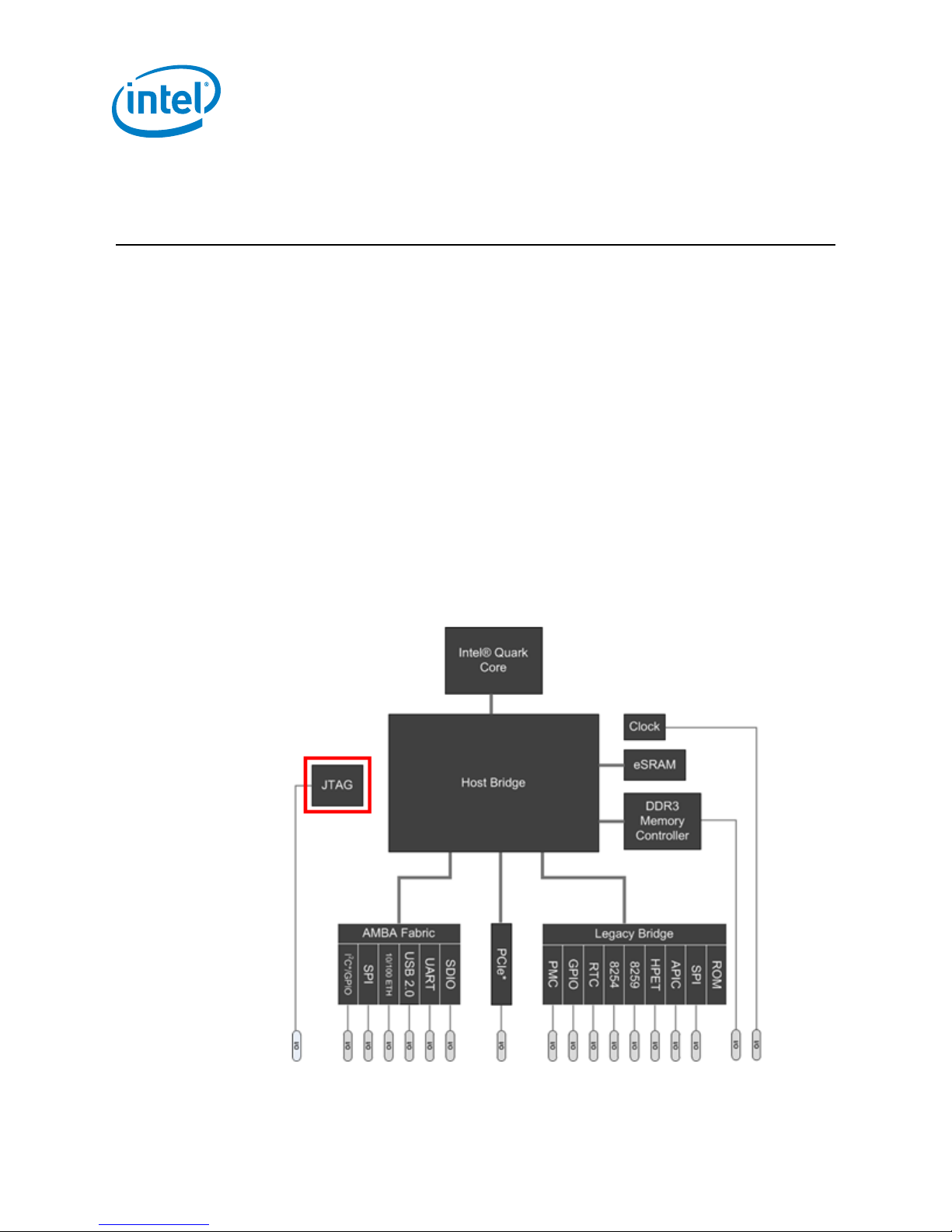
1 Introduction
Introduction
The Intel
Intel
®
Quark SoC X1000 processor is the next generation secure, low-power
®
Architecture (IA) SoC for deeply embedded applications. The SoC integrates the
Intel® Quark SoC X1000 Core plus all the required hardware components to run offthe-shelf operating systems and to leverage the vast x86 software ecosystem. For
details, see the Intel® Quark SoC X1000 Datasheet.
The Intel® Quark SoC X1000 Core (codenamed Lakemont) enables a range of lowcost, high-performance embedded system designs capable of running applications
written for the Intel architecture. The Intel® Quark SoC X1000 Core integrates a 16Kbyte unified cache and floating-point hardware onchip for improved performance. For
further details, including the Intel® Quark Core feature list, see the Intel® Quark SoC
X1000 Core Hardware Reference Manual and Intel® Quark SoC X1000 Core
Developer’s Manual.
This document assumes that the reader has some familiarity with JTAG based debug
tools and the use of JTAG for run control of an execution core.
This document provides details on JTAG based debug for any product based on the
Intel® Quark SoC X1000.
Figure 1. Intel® Quark SoC X1000
4 Order Number: 329866-002US
Page 5
Term
Description
ACPI Sx states
System sleep states as defined by the ACPI standard:
http://www.acpi.info/
CLTAPC
Chip level TAP Controller. This is the top level standard compliant TAP
controller for the SoC.
Debug Software
Generic term for software that controls a hardware probe connected to
the JTAG pins.
JTAG
“Joint Test Action Group” of the IEEE. This is now a generic term to
refer to the TAP and the pins used for communication with TAPs.
PIR
Probe Mode Instruction Register
PRDY#
Probe Mode Ready package pin (active low); this pin is used to signal
to Debug Software that the core has entered Probe Mode
PREQ#
Probe Mode Request package pin (active low); this pin may be used by
Debug Software to request that the core enter Probe Mode
SoC
System on chip
TAP
Test Access Port as defined by the IEEE 1149.1-1990 (including IEEE
1149.1a-1993), “IEEE Standard Test Access Port and Boundary-Scan
Architecture”
TDI
TAP Data In; the serial data input pin for the TAP chain
TDO
TAP Data Out; the serial data output pin for the TAP chain
TDR
TAP Data Register; a serial TAP data register selected by a TAP
instruction
Title and Location
Document #
Intel® Quark SoC X1000 Datasheet
https://communities.intel.com/docs/DOC-21828
329676
Intel® Quark SoC X1000 Core Hardware Reference Manual
https://communities.intel.com/docs/DOC-21825
329678
Intel® Quark SoC X1000 Core Developer’s Manual
https://communities.intel.com/docs/DOC-21826
329679
Introduction
1.1 Terminology
Table 1. Terminology
1.2 Related Documents
Table 2. Related Documents
Order Number: 329866-002US 5
Page 6

Title and Location
Document #
Intel® 64 and IA-32 Architectures Software Developer Manuals contain
details on architectural registers:
http://www.intel.com/content/www/us/en/processors/architecturessoftware-developer-manuals.html
Multiple
volumes
Introduction
6 Order Number: 329866-002US
Page 7

Function/Category
Instruction Mnemonic
Opcode (8 bits)
TDR Name
SOC IDCODE
CLIDCODE
0x02
CLIDCODE
BYPASS
CLBYPASS
0xFF
CLBYPASS
TAP NETWORK
CLTAPC_SELECT
0x11
CLTAPC_SELECT
IA Run Control
CLTAPC_CPU_VPREQ
0x51
CLTAPC_CPU_VPREQ
CLTAPC_CPU_TAPSTATUS
0x52
CLTAPC_CPU_TAPSTATUS
CLTAPC_CPU_VPRDY
0x53
CLTAPC_CPU_VPRDY
TapNW Status
CLTAPC_TAPNW_STATUS
0x69
CLTAPC_TAPNW_STATUS
RESERVED
-
All other values
-
JTAG Interface
2 JTAG Interface
The Intel® Quark SoC X1000 has the standard set of JTAG pins, TCLK, TDI, TDO, TMS,
and TRST# on the package which are routed to a debug header on the system board.
The SoC exposes a single IEEE compliant TAP by default, called the ‘Chip-Level TAP
Controller’ (CLTAPC). This TAP provides some basic system status and has the ability
to ‘add’ child TAP controllers to the serial JTAG chain.
Debug Software tools that wish to provide run control for the Intel® Quark SoC X1000
must interact with the CLTAPC to add the CPU core to the JTAG chain. The Debug
Software may also use TAP data registers (TDRs) in the CLTAPC to monitor system
status. The CLTAPC provides some features related to run control of the core which is
described in detail in Section 5.
2.1 SKU-Based JTAG Debug Capability
Not all SKUs of the Intel® Quark SoC X1000 ship with JTAG debugging enabled. To
receive details on how to enable JTAG on these SKUs, contact your Intel account
team.
2.2 CLTAPC Instruction Table
Table 3. CLTAPC TAP Instructions
Order Number: 329866-002US 7
Page 8
2.3 CLTAPC Data Register Table
TDR Name
TDR Length (Bits)
Reset Mechanism
Access
CLIDCODE
32b
TRST/SYNC TAP RST
Read-Only
CLBYPASS
1b
TRST/SYNC TAP RST
Read-Write
CLTAPC_SELECT
64b
TRST/SYNC TAP RST
Read-Write
CLTAPC_CPU_VPREQ
8b
PWR_GOOD†
Read-Write
CLTAPC_CPU_TAPSTATUS
8b
PWR_GOOD†
Read-Only
CLTAPC_CPU_VPRDY
1b
PWR_GOOD†
Read-Write
CLTAPC_TAPNW_STATUS
64b
PWR_GOOD†
Read-Write
† The external power supply signal is used for PWR_GOOD. These values survive a board reset if
the power supply is still connected to the board.
CLTAPC_SELECT
Bit Number
Name
Reset Value
Comments
1:0
CPUCORE_TAP_SEL
2'b00
2'b01 = Normal;
2'b10 = Excluded;
2'b11 = Shadow
63:2
RESERVED
2'b00
RESERVED
Table 4. CLTAPC TAP Data Registers
2.3.1 CLIDCODE
JTAG Interface
The CLTAPC IDCODE register is 32 bits in size. This value may be used by Debug
Software to confirm there is a working JTAG connection to the board and to confirm
the identity of the SoC.
The Intel® Quark SoC X1000 IDCODE is 0x0E681013.
2.3.2 CLBYPASS
This is the IEEE standard BYPASS data register; it is one bit in size.
2.3.3 CLTAPC_SELECT
This data register contains bits that control the presence of the children TAPs in the
SoC on the JTAG chain.
Table 5. CLTAPC_SELECT
When bits 1:0 are set to the value 01 by Debug Software, the CPU Core TAP is added
to the JTAG chain immediately after the CLTAPC.
8 Order Number: 329866-002US
Page 9

CLTAPC_CPU_VPREQ
Bit Number
Name
Reset Value
Comments
0
assert_vpreq
1'b0
Assert PREQ to Core
1
enable_preq_on_reset
1'b0
Enable PREQ assertion on Reset
2
enable_preq_on_reset_2
1'b0
Enable PREQ assertion Reset
Source 2
7:3
RESERVED
1'b0
RESERVED
JTAG Interface
The chain order becomes TDI CLTAPC CPU_CORE_TAP TDO.
All other bits in this register are reserved.
2.3.4 CLTAPC_CPU_VPREQ
The CLTAPC has control over an internal PREQ wire connected to the core. This
provides Debug Software the ability to use some PREQ based debug features when
connected using JTAG pins alone.
This data register contains bits that control the assertion of the internal ‘PREQ’ signal
to the Intel® Quark SoC X1000 Core and reset break behavior.
Table 6. CLTAPC_CPU_VPREQ
When bit 0 is set to 1 by Debug Software, the PREQ signal connected to the core will
be asserted. This signal is an external request to the core that causes the core to
break and enter Probe Mode.
Arm resetbreak for the core by setting bits ‘enable_preq_on_reset’ (bit 1) and
‘enable_preq_on_reset_2’ (bit 2). When these bits are set and the core receives a
RESET event, the Core will immediately break and enter Probe Mode instead of
executing the first instruction. The core will enter Probe Mode with the CS register set
to 0xF000 and the EIP register set to 0x0000FFF0. The instruction located at this
address has not been executed when a resetbreak triggered the entry to Probe Mode.
All other bits in this register are reserved.
Order Number: 329866-002US 9
Page 10

CLTAPC_CPU_TAPSTATUS
Bit Number
Name
Reset Value
Comments
0
vpreq_asserted
1'b0
PREQ was asserted via one
of the sources in
CPU_VPREQ
1
prdy_asserted
1'b0
PRDY was asserted by the
Core
2
preq_asserted_via_reset
1'b0
PREQ was asserted via
Reset Source 1.
3
preq_asserted_via_reset_2
1'b0
PREQ was asserted via
Reset Source 2.
7:4
RESERVED
4’b0000
RESERVED
2.3.5 CLTAPC_CPU_TAPSTATUS
This data register contains status bits related to the Run Control features in the
CLTAPC_CPU_VPREQ register.
Table 7. CLTAPC_CPU_TAPSTATUS
JTAG Interface
2.3.6 CLTAPC_CPU_VPRDY
This data register is used to reset the status bits in the CLTAPC_CPU_TAPSTATUS
register when it is written to. It is a single bit in size, but the value written does not
matter.
2.3.7 CLTAPC_TAPNW_STATUS
This data register contains a mixture of status bits. Bit 0 will be 1 when the Core TAP
has been added to the JTAG chain using the CLTAPC_SELECT instruction.
Bits 33 to 34 provide details on the current ACPI Sx state. The Core is awake and
running only when the SoC/System is in S0, `S0_power_ok’ (bit 34) is 1.
Bit 35 must be 1 before the Core TAP may be added to the JTAG Chain.
If the Core is not awake, it cannot be added to the JTAG chain and cannot be available
for run control.
10 Order Number: 329866-002US
Page 11

CLTAPC_TAPNW_STATUS
Bit Number
Name
Reset
Value
Comments
0
cltapnw_en[CPUCORETAP_SEL]
0x0
Returns 1 when the
IA Core TAP is in the
JTAG Chain
31:1
RESERVED
0x0
RESERVED
32
S5_power_ok
0x0
S5_power_ok Status
33
S3_power_ok
0x0
S3_power_ok Status
34
S0_power_ok
0x0
S0_power_ok Status
35
jtag_valid
0x0
When the SoC is in
S0, this bit must be 1
before the Core TAP
may be added to the
JTAG chain
63:36
RESERVED
0x0
RESERVED
JTAG Interface
Table 8. CLTAPC_TAPNW_STATUS
Order Number: 329866-002US 11
Page 12

3 Putting It All Together
This section uses the reference information from Section 2 to put together all of the
steps required for Debug Software to prepare the target for Core run control.
3.1 Initial JTAG Discovery
There are two methods available for Debug Software to confirm that it has a good
connection to the Chip-Level TAP Controller before moving on to debug the Intel®
Quark SoC X1000 Core.
Using a TAP Reset
Issue a JTAG reset by asserting and then de-asserting the TRST# pin, or by
holding TMS to 1 for five TCLK cycles. Both mechanisms are part of the IEEE
1149.1 standard for a TAP reset.
Use a 32 bit or DR Shift using the TAP finite state machine and examine the
data captured on TDO. It should match the Intel® Quark SoC X1000 CLTAPC
IDCODE (0x0E681013).
Without a TAP Reset
Shift in the IR Opcode for the CLTAPC IDCODE data register (0x2) and then a
32 bit DR Shift. The data collected on TDO should match the CLTAPC IDCODE.
Putting It All Together
3.2 Check Core Powergood
Once the Debug Software has verified that it has a working connection to the SoC, it
can check to see if the Core is powered.
Using a JTAG DR Shift to read the CLTAPC_TAPNW_STATUS data register, check that
bit 34, `S0_power_ok’ is set to 1. When this bit is a 1, it is safe to access the Core’s
TAP.
3.3 Add Core TAP to the JTAG Chain
The Core TAP is added to the JTAG chain by setting its ‘select’ bits in the
CLTAPC_SELECT data register. The data value used to add the core is the 64 bit
value: 0x00000000_00000001. The Core TAP is added to the JTAG chain when the
TAP finite state machine (FSM) enters Update-DR. The Debug Software should move
the TAP FSM to Run-Test/Idle immediately after writing any bits in CLTAPC_SELECT.
Until the select bits are cleared, Debug Software must be prepared to account for the
fact that there are two TAPs on the chain.
12 Order Number: 329866-002US
Page 13

Putting It All Together
3.4 Verify Core IDCODE
After completing the steps above, the Debug Software can then verify that the Core
TAP is in the JTAG chain. The 8 bit IR Opcode for the Core IDCODE data register is
0x2. The Core IDCODE value is 0x18289013.
Order Number: 329866-002US 13
Page 14

4 JTAG Interface
IR Opcode
TAP
Command
Description
DR Size
(Bits)
Values
0x02
IDCODE
The IEEE 1149 compliant
IDCODE
32 0x03
SUBMITPIR
Submit the contents of the
PIR to the core
0
0x04
PROBEMODE
Enter and Exit Probe Mode
(Details in Section 5.1)
1
1: Enter Probe Mode
0: Exit Probe Mode
0x06
WRITEPIR
Write instruction opcodes to
the PIR
64
0x08
RWPDR
Select the PDR chain for read
or write
32
0x0B
TAPSTATUS
TAP Status register
32
See Table 10.
0xFF
BYPASS
IEEE 1149 BYPASS instruction
1
All other values
BYPASS
IEEE 1149 BYPASS instruction
1
4.1 TAP Instruction Table
The Intel® Quark SoC X1000 Core TAP uses an 8-bit instruction register. The following
table describes all IR opcode encodings.
Table 9. TAP Instructions
JTAG Interface
14 Order Number: 329866-002US
Page 15

Run Control
5 Run Control
5.1 Introduction to Probe Mode
Probe Mode is a debug mode of the processor in which the normal execution sequence
is interrupted. The processor enters a dormant state where architectural state can be
viewed and modified. The state extraction/modification is performed with the help of
the TAP. Special hardware/software products are developed to make use of Probe
Mode.
The processor can be made to enter Probe Mode in various ways. The PREQ (Probe
Mode Request) pin, called PREQ# is pulsed to cause Probe Mode entry. The processor
can also be configured to enter Probe Mode when certain events occur (redirecting to
Probe Mode).
Once the processor enters Probe Mode and is ready to accept commands, it pulses the
PRDY (Probe Mode Ready) pin, called PRDY#. Debug Software can then issue Probe
Mode instructions (to be described later) to access architectural state. When an
instruction is submitted while the processor is in Probe Mode, PRDY# is pulsed upon
completion of the instruction.
While in Probe Mode, all the communication between the Debug Software and the
processor is done through the TAP. The Probe Mode instructions are serially sent via
the WRSUBPIR instruction into the TAP that then transfers the instruction bytes to the
fetch unit.
Probe Mode Entry on Intel processors is an interrupt/exception style event and is
prioritized with other events. The priority is very low.
5.2 Probe Mode Entry
Probe Mode may be entered asynchronously (from the Core’s perspective) by the
request of debug software using two mechanisms: the PREQ# pin and the TAP. Both
the CLTAPC and the Core TAP in the Intel® Quark SoC X1000 have TAP instructions for
requesting entry into Probe Mode.
Some systems using the Intel® Quark SoC X1000 may not route the PREQ# and
PRDY# pins to the Debug Tool’s connector on the board. In these cases, the Debug
Software must rely only on the TAP for all debug activities.
The Core will pulse PRDY# for two bus clock cycles and this pulse is latched by the
CLTAPC_CPU_TAPSTATUS TDR.
The Core may be configured to enter Probe Mode when a code or data breakpoint
match occurs. These appear to be asynchronous entries in to Probe Mode from the
perspective of the Debug Software since it cannot predict when or if the breakpoint
match will occur. Any standard Debug Exception (#DB) from the core may be
Order Number: 329866-002US 15
Page 16

configured to cause an entry to Probe Mode instead of allowing the exception handler
Bit Field
Description
31:7
Reserved
6
Shutdown Break Occurred. This bit is set to ‘1 when a shutdown break was the
cause for the break.
5
Shutdown Break is enabled. This is a copy of PMCR[1]
4
If ‘1, the core supports software breakpoints installed by debug software
3
Probe Mode Redirection. Holds value of PMCR[0].
2
Probe Mode In Progress. Held high while in Probe Mode and after register state
has been saved to shadow SRAM.
to run. See the Probe Mode Control Register section below for full details.
The PREQ pin must be pulsed to enter Probe Mode. The PROBEMODE TAP instruction
offers a TAP-based entry method as an alternative. To use the TAP-based Probe Mode
entry, write ‘1 to the PROBEMODE data register. The core will automatically redirect to
Probe Mode after a single step, hardware or software breakpoint. All entries to Probe
Mode are signaled to the Run Control Hardware via the PRDY# pin.
Note: The core requires that TCLK be running for it to latch PREQ# pin events for Probe
Mode entry.
5.3 Probe Mode Exit
Probe Mode exit is accomplished by writing a ‘0 to the PROBEMODE TAP instruction’s
data register. Reset will also cause the core to leave Probe Mode.
5.4 Reset Break
Run Control
In order to debug BIOS or firmware from the first instruction, the reset break
capability must be used. The Intel® Quark SoC X1000 Core supports reset break with
two mechanisms. The first option depends on the PREQ# and PRDY# signals being
connected to the Hardware Probe. The second option is available for when the Debug
Tool is connected using only the JTAG pins.
Mechanisms for reset break:
1. Run Control hardware must monitor the target for RESET events so that it may
assert PREQ# prior to the rising edge of RESET# as sampled by the core.
2. Use the CLTAPC_CPU_VPREQ TDR detailed in Section 2.3.4.
5.5 TAPSTATUS Register
The TAPSTATUS register is defined in the following table.
Table 10. TAPSTATUS Data Register
16 Order Number: 329866-002US
Page 17

Bit Field
Description
1
Probe Mode Request. Held high on Enter Probe Mode Request, reset once register
state has been saved to shadow SRAM.
0
Probe Mode Ready, this is a copy of the PRDY# signal. Since PRDY# is pulsed for
a short number of clocks this may never be seen as ‘1.
Run Control
5.6 Accessing Architectural Registers
The architectural registers are copied to an internal SRAM upon entry to Probe Mode
and may be accessed in any order. Debug software must cache the values of any
register that may be changed in the SRAM during Probe Mode operations like memory
access. These cached values must be written to the SRAM prior to releasing the
processor from Probe Mode when handling the ‘go’ command. Full details on register
reads and writes are in Section 5.6.5 and Section 5.6.6.
5.6.1 Submitting Instructions to the Core
The Probe Mode Instruction Register (PIR) is used via two TAP instructions:
The WRITEPIR TAP data register allows the debug tool to write instruction opcodes
into the TAP. Once the WRITEPIR data register is populated, the opcodes are
submitted to the core for execution using the SUBMITPIR TAP instruction.
SUBMITPIR is an ‘IR Only’ TAP command; there is no corresponding data register.
The following instructions are supported by the Core while in Probe Mode:
Memory Read and Write via MOV r, m8/m16/m32 and MOV m8/m16/m32, r
I/O Read and Write via IN and OUT
MSR Read and Write via RDMSR and WRMSR
The WBINVD and INVVD instructions
The CPUID instruction
Note: The PG bit in the CR0 register must be 0 before submitting instructions to the core for
execution.
5.6.1.1 Instruction Faults
Instructions submitted via the TAP that are executed by the core may generate faults.
The debug software should make every attempt to verify that instructions used by the
software internally do not fault. However, the user is free to submit any instruction or
data that may result in a fault. Some potential faults: page fault, segment violation, or
accessing an undefined MSR.
If a fault occurs:
The core will not re-enter Probe Mode and Run Control Hardware will not see a
pulse on the PRDY# pin.
Order Number: 329866-002US 17
Page 18

The core may enter the SHUTDOWN state, depending on the side effects of the
fault. For example, if a valid IDT is not set up or the fault handlers are not present
in memory, the core may enter SHUTDOWN.
Debug software can watch for PRDY# timeouts after submitting instructions to the
core. If a timeout occurs, debug software may attempt to force the core back into
Probe Mode via the PREQ# pin or the PROBEMODE TAP instruction. If the core has
entered SHUTDOWN, there may be no other option other than resetting the core to
restart instruction execution.
5.6.2 EIP Management
The core automatically resets EIP after each instruction while in Probe Mode. This is
done to prevent segment violations and triggering breakpoints while in Probe Mode.
5.6.3 DR7 Management
While the core is in Probe Mode, debug software must write the value of 0x00000000
to the DR7 register. This is needed to disable any data or I/O breakpoints while the
core is halted. This is the reset value for DR7 for this architecture.
Run Control
5.6.3.1 EIP and Software Breakpoints
Software breakpoints behave as instruction traps in the Intel® Quark SoC X1000 Core.
After entering Probe Mode due to a software break point trigger, the EIP register
points to the instruction immediately after the 0xF1 opcode used for the breakpoint.
Debug software must check for software breakpoint matches using EIP – 1 when
determining the break cause and replacing the displaced opcode byte when resuming
execution from the break address.
5.6.4 WRITEPIR Register Format
The 64-bit WRITEPIR TAP data register allows ITP to submit instruction opcodes for
execution by the core. If the instruction submitted by Debug software does not use all
64 bits, the remaining bytes must be ‘padded’ with NOP instructions, opcode 0x90.
The data value must be transformed using a two-step process prior to the addition of
the NOP pads.
The following sample using the instruction MOV EAX, DWORD PTR [EDX] illustrates
this process.
The opcodes for this instruction used in this sample are 0x66678B02.
Rearrange the byte order, moving the least significant byte to the most significant
byte:
0x66678B02 becomes 0x20B87666
Reverse the bits in each byte:
0x20B87666 becomes 0x40D1E666
Add the NOP opcode to create the full 64 bit value:
0x40D1E666 becomes 0x0909090940D1E666
18 Order Number: 329866-002US
Page 19

Run Control
5.6.5 Register Read
The template to read a register:
1. Find the PIR value for the desired register in Table 11 below.
a. Use WRITEPIR to shift in the 64-bit value from the table.
b. Shift in SUBMITPIR TAP instruction.
2. Write the ‘SRAMACCESS’ pseudo opcode (from Table 11 below) to the PIR.
3. Shift in SUBMITPIR TAP instruction.
4. Write the ‘SRAM2PDR’ pseudo opcode (from Table 11 below) to the PIR.
5. Shift in SUBMITPIR TAP instruction.
6. Use the RWPDR TAP instruction to read the 32 bits of data.
5.6.6 Register Write
The template to write a register:
1. Shift the data to be written in to the TAP PDR.
2. Find the PIR value for the desired register in Table 11 below.
a. Use WRITEPIR to shift in the 64-bit value from the table.
b. Shift in SUBMITPIR TAP instruction.
3. Write the ‘SRAMACCESS’ pseudo opcode (from Table 11 below) to the PIR.
4. Shift in SUBMITPIR TAP instruction.
5. Write the ‘PDR2SRAM’ pseudo opcode (from Table 11 below) to the PIR.
6. Shift in the SUBMITPIR TAP instruction.
5.6.7 Special Cases for Register Access
5.6.7.1 PMCR
This register in the SRAM is write-only; reads return all zeros.
5.6.7.2 Register Access after HLT Instruction Execution
If the core has executed the HLT instruction and is in the ‘HALT’ state when Probe
Mode entry occurs, the following registers are read-only in the SRAM:
CR2
DR0-DR3 (hardware breakpoints may not be added or removed in this state)
PMCR
See Checking for HALT State below for details.
Order Number: 329866-002US 19
Page 20

5.6.8 Checking for HALT State
When the core executes the HLT instruction, it stops instruction execution and places
the processor in a HALT state. Any of the following will resume execution:
Enabled interrupt (including NMI and SMI)
Debug exception
BINIT# signal
INIT# signal
RESET# signal
If an interrupt (including NMI) is used to resume execution after a HLT instruction, the
saved instruction pointer (CS:EIP) points to the instruction following the HLT
instruction.
The core also emits a special bus cycle alerting other agents on the bus that the core
has entered HALT. This will be used by SoCs integrating the core to clock gate and/or
power down the core. Because the core is powered down or clock-gated while in the
HALT state, debug software may never find the core is in HALT after entering Probe
Mode.
Run Control
The debugger can determine if the core is in HALT by reading the HALT register from
the SRAM and checking bit 16. If bit 16 is 1, the core is in the HALT state.
5.6.9 Pseudo Opcodes for Architectural Register Access
Each register in Table 11 is described in detail in the Intel Software Developer’s
Manuals here: http://www.intel.com/content/www/us/en/processors/architectures-
software-developer-manuals.html
20 Order Number: 329866-002US
Page 21

Register
64 Bit PIR Value
Register
64 Bit PIR Value
Register
64 Bit PIR Value
CR0
0x000000001D660000
TSSlimit
0x000000181D660000
CSlimit
0x0000000C1D660000
CR3
0x000000801D660000
IDTar
0x000000981D660000
ESar
0x0000008C1D660000
EFLAGS
0x000000401D660000
IDTbase
0x000000581D660000
ESbase
0x0000004C1D660000
EIP
0x000000C01D660000
IDTlimit
0x000000D81D660000
ESlimit
0x000000CC1D660000
EDI
0x000000201D660000
GDTar
0x000000381D660000
CR4
0x0000002C1D660000
ESI
0x000000A01D660000
GDTbase
0x000000B81D660000
SIP
0x000000AC1D660000
EBP
0x000000601D660000
GDTlimit
0x000000781D660000
TMPD
0x0000006C1D660000
ESP
0x000000E01D660000
LDTar
0x000000F81D660000
TMPB
0x000000EC1D660000
EBX
0x000000101D660000
LDTbase
0x000000041D660000
TMPC
0x0000001C1D660000
EDX
0x000000901D660000
LDTlimit
0x000000841D660000
HALT
0x0000009C1D660000
ECX
0x000000501D660000
GSar
0x000000441D660000
REV
0x0000005C1D660000
EAX
0x000000D01D660000
GSbase
0x000000C41D660000
BASE
0x000000DC1D660000
DR6
0x000000301D660000
GSlimit
0x000000241D660000
PDR6
0x0000003C1D660000
DR7
0x000000B01D660000
FSar
0x000000A41D660000
CR2
0x000000BC1D660000
TR
0x000000701D660000
FSbase
0x000000641D660000
DR0
0x0000007C1D660000
LDTR
0x000000F01D660000
FSlimit
0x000000E41D660000
DR1
0x000000FC1D660000
GS
0x000000081D660000
DSar
0x000000141D660000
DR2
0x000000021D660000
FS
0x000000881D660000
DSbase
0x000000941D660000
DR3
0x000000821D660000
DS
0x000000481D660000
DSlimit
0x000000541D660000
PMCR
0x000000421D660000
SS
0x000000C81D660000
SSar
0x000000D41D660000
SRAMACCESS
0x0000000E9D660000
CS
0x000000281D660000
SSbase
0x000000341D660000
SRAM2PDR
0x4CF0000000000000
ES
0x000000A81D660000
SSlimit
0x000000B41D660000
PDR2SRAM
0x0CF0000000000000
TSSar
0x000000681D660000
CSar
0x000000741D660000
TSSbase
0x000000E81D660000
CSbase
0x000000F41D660000
Run Control
Table 11. Register Access PIR Values
5.6.10 Probe Mode Control Register
This register contains only one bit: the IR bit. When this bit is set, all debug
exceptions (#DB) are converted to Probe Mode entry. This bit must be set for all types
of instruction steps and when hardware breakpoints are installed. If the core adds
support for software breakpoints, this bit would be set to enable them as well.
This register is accessible via the TAP and through the SRAM. The pseudo opcode PIR
value for this register in the SRAM is 0x000000421D660000.
Order Number: 329866-002US 21
Page 22

PMCR
Description
Bit 0
IR bit, when set all debug exceptions are converted into Probe Mode entry event.
Bit 1
Shutdown Redirection, when this bit is set to ‘1 SHUTDOWN events cause an entry
to Probe Mode.
Table 12. PMCR Description
5.6.11 Accessing Model Specific Registers (MSR)
MSRs may be accessed (read and written) using the following flow:
1. Write the MSR index value to the ECX register using normal SRAM write operation.
2. Read:
a. Submit an ‘rdmsr’ instruction to the core via WRITEPIR and SUBMITPIR.
b. Bits 31:0 of the MSR data will be in EAX; bits 63:32 of the MSR data will be
EDX.
3. Write:
a. Move bits 31:0 of the data to be written to EAX; move bits 63:32 of the data
to EDX.
b. Submit a ‘wrmsr’ instruction to the core via WRITEPIR and SUBMITPIR.
Run Control
5.7 Reading and Writing Memory
Memory may be read and written using the Intel® Quark SoC X1000 Core by direct
injection of the macro-instructions via the TAP’s PIR register. The core will:
1. Restore all register states from the shadow SRAM.
2. Exit Probe Mode.
3. Execute the single instruction.
4. Re-enter Probe Mode.
5. When the re-entry to Probe Mode completes, the PRDY# pin is pulsed to indicate
to debug software that the core is ready for the next instruction.
If the memory access fails, the PRDY# pin will not signal that the instruction
completed. Debug software may use this to detect failures and attempt to force the
core back into Probe Mode or let the user know that the core must be reset.
5.7.1 Management of Architectural Registers for Memory Access
All register reads and writes used as part of memory accesses are performed using the
pseudo opcodes to interact with the SRAM. Only the MOV instructions used for the
actual read or write are executed by the core. The MOV instructions must be written to
the WRITEPIR data register using the standard NOP padding and byte reversal.
22 Order Number: 329866-002US
Page 23

Register
Value
DS Base
0x00000000
DS Limit
0xFFFFFFFF
DS AR
0x004F9300
Run Control
5.7.1.1 DS Selector
The DS selector must be changed before debug software can access the full 4GB
address space while in Probe Mode. Prior to any memory access, the registers listed in
the following table must be set to the values specified for each. Debug software must
take care to read these registers after Probe Mode entry and cache the values so that
they may be restored prior to Probe Mode exit.
Table 13. DS Selector Values for Memory Access
5.7.1.2 Adjust CPL Prior to Memory Access
The code-privilege level in effect prior to Probe Mode entry may prevent the use of the
WBINVD instruction needed to flush the cache. Debug software must set the CPL to 0
in both the CS access byte and the SS access byte if they are non-zero as part of the
architectural save-state process. This is done by changing bits 13 and 14 in the SSAR
and CSAR registers to zero. If they are zero upon Probe Mode entry, Debug software
does not need to change them.
5.7.1.3 Disable Interrupts Prior to Memory Access
The processor must not be allowed to handle pending interrupts when it is released
from Probe Mode to handle memory reads/writes. Interrupt handling is disabled by
setting the IF bit in the EFLAGS register to 0.
5.7.1.4 Processor Cache Flush Prior to Memory Access
If enabled prior to Probe Mode entry, the cache must be flushed and disabled prior to
any memory access from ITP. If the CR0.CD bit is 0, the following steps must be
performed:
1. Perform the actions described in Sections 5.7.1.1, 5.7.1.2, and 5.7.1.3.
2. Set CR0.PG to 0, if it is 1.
3. Submit WBINVD instruction.
4. Set CR0.NW and CR0.CD bit.
5. Set CR0.PG to 1, if it had been 1 in step 2.
Debug software must restore all architectural registers to the values they contained
after Probe Mode entry before releasing the core to continue normal execution.
5.7.1.5 CR0
The value of the CR0.PG (paging enabled) bit influences memory reads and writes. To
read from a physical memory address provided by the user or during address
translation, Debug software must set the CR0.PG to bit to ‘0. Memory reads and writes
Order Number: 329866-002US 23
Page 24

using linear, two-field virtual, and three-field virtual must first be translated to the
physical address form before being used to read or write memory.
5.7.2 Memory Read
1. Clear CR0.PG bit if is it 1.
2. Write address to EAX.
3. Submit the read instruction to the core: MOV EDX, DWORD PTR [EAX].
4. Read memory data from EDX via the SRAM and PDR.
5. Restore CR0.PG bit if it was changed in the first step.
5.7.3 Memory Write
1. Clear CR0.PG bit if it is 1.
2. Write address to EAX.
3. Write data to EDX.
4. Submit the memory write instruction to the core: MOV DWORD PTR [EAX], EDX.
5. Restore the CR0.PG bit if it was changed in the first step.
Run Control
5.8 Reading and Writing I/O Ports
The Intel® Quark SoC X1000 Core supports I/O port reads and writes using the IN and
OUT instructions submitted to the core via the TAP.
Note: The CR0.PG bit must be 0 prior to using the PIR TAP instructions to submit I/O read
and write instructions.
5.8.1 I/O Read
1. Write the I/O address to read from to the DX register.
2. Submit one of the following based on the desired access width:
1 byte wide read: IN AL, DX
2 byte wide read: IN AX, DX
4 byte wide read: IN EAX, DX
5.8.2 I/O Write
1. Write the I/O address for the write to the DX register.
2. Write the data to be written to the EAX register.
3. Submit one of the following based on the desired access width:
1 byte wide write: OUT DX, AL
2 byte wide write: OUT DX, AX
4 byte wide write: OUT DX, EAX
24 Order Number: 329866-002US
Page 25

Run Control
5.9 Hardware Breakpoints
1. Write the linear address to DR0-3.
2. Set DR6 and DR7 bits as needed.
3. Set bit 0 in PMCR to convert the #DB exception to a Probe Mode entry.
5.10 Software Breakpoints
To determine if an instance of the Intel® Quark SoC X1000 Core supports software
breakpoints, check bit 4 in the TAPSTATUS register. If the bit is ‘1, the core supports
software breakpoints.
Configure software breakpoints in the Core by replacing one byte of the original
instruction opcode(s) in memory with the value 0xF1 and setting PMCR[IR] to ‘1.
5.11 Single Step
1. Set EFLAGS[TF] to ‘1 and PMCR[IR] to ‘1.
2. Release from Probe Mode and wait for PRDY#.
On Probe Mode entry from SW break, debug software must decrement EIP by 1 before
replacing the 0xF1 with the real opcode byte.
5.12 Redirections into Probe Mode
5.12.1 Shutdown Break
The processor may be configured to enter Probe Mode when a SHUTDOWN event
occurs. This is enabled by setting bit 1 in the PMCR register to ‘1.
To determine if the cause for an asynchronous entry into Probe Mode was caused by a
shutdown break, bit 6 in the TAPSTATUS data register will be set to ‘1. PMCR bit 5
holds a copy of the enable bit in PMCR. This allows debug software to check if the
shutdown redirection is enabled without putting the core into Probe Mode.
Order Number: 329866-002US 25
Page 26

Revision History
Date
Revision
Description
January 2014
002
Added value for CSar in Table 11.
November 2013
001
First release of document.
Revision History
INFORMATION IN THIS DOCUMENT IS PROVIDED IN CONNECTION WITH INTEL PRODUCTS. NO LICENSE, EXPRESS OR IMPLIED,
BY ESTOPPEL OR OTHERWISE, TO ANY INTELLECTUAL PROPERTY RIGHTS IS GRANTED BY THIS DOCUMENT. EXCEPT AS
PROVIDED IN INTEL'S TERMS AND CONDITIONS OF SALE FOR SUCH PRODUCTS, INTEL ASSUMES NO LIABILITY WHATSOEVER
AND INTEL DISCLAIMS ANY EXPRESS OR IMPLIED WARRANTY, RELATING TO SALE AND/OR USE OF INTEL PRODUCTS
INCLUDING LIABILITY OR WARRANTIES RELATING TO FITNESS FOR A PARTICULAR PURPOSE, MERCHANTABILITY, OR
INFRINGEMENT OF ANY PATENT, COPYRIGHT OR OTHER INTELLECTUAL PROPERTY RIGHT.
A "Mission Critical Application" is any application in which failure of the Intel Product could result, directly or indirectly, in
personal injury or death. SHOULD YOU PURCHASE OR USE INTEL'S PRODUCTS FOR ANY SUCH MISSION CRITICAL
APPLICATION, YOU SHALL INDEMNIFY AND HOLD INTEL AND ITS SUBSIDIARIES, SUBCONTRACTORS AND AFFILIATES, AND THE
DIRECTORS, OFFICERS, AND EMPLOYEES OF EACH, HARMLESS AGAINST ALL CLAIMS COSTS, DAMAGES, AND EXPENSES AND
REASONABLE ATTORNEYS' FEES ARISING OUT OF, DIRECTLY OR INDIRECTLY, ANY CLAIM OF PRODUCT LIABILITY, PERSONAL
INJURY, OR DEATH ARISING IN ANY WAY OUT OF SUCH MISSION CRITICAL APPLICATION, WHETHER OR NOT INTEL OR ITS
SUBCONTRACTOR WAS NEGLIGENT IN THE DESIGN, MANUFACTURE, OR WARNING OF THE INTEL PRODUCT OR ANY OF ITS
PARTS.
Intel may make changes to specifications and product descriptions at any time, without notice. Designers must not rely on the
absence or characteristics of any features or instructions marked "reserved" or "undefined". Intel reserves these for future
definition and shall have no responsibility whatsoever for conflicts or incompatibilities arising from future changes to them. The
information here is subject to change without notice. Do not finalize a design with this information.
The products described in this document may contain design defects or errors known as errata which may cause the product to
deviate from published specifications. Current characterized errata are available on request.
Contact your local Intel sales office or your distributor to obtain the latest specifications and before placing your product order.
Copies of documents which have an order number and are referenced in this document, or other Intel literature, may be obtained
by calling 1-800-548-4725, or go to: http://www.intel.com/design/literature.htm
Intel, and the Intel logo are trademarks or registered trademarks of Intel Corporation or its subsidiaries in the United States and
other countries.
*Other names and brands may be claimed as the property of others.
Copyright © 2014, Intel Corporation. All rights reserved.
26 Order Number: 329866-002US
 Loading...