

Page 1

Intel NetStructure® MPCBL0001
High Performance Single Board
Computer
Technical Product Specification
May 2006
Order Number: 273817-010
Page 2

INFORMATION IN THIS DOCUMENT IS PROVIDED IN CONNECTION WITH INTEL® PRODUCTS. NO LICENSE, EXPRESS OR IMPLIED, BY
ESTOPPEL OR OTHERWISE, TO ANY INTELLECTUAL PROPERTY RIGHTS IS GRANTED BY THIS DOCUMENT. EXCEPT AS PROVIDED IN
INTEL'S TERMS AND CONDITIONS OF SALE FOR SUCH PRODUCTS, INTEL ASSUMES NO LIABILITY WHATSOEVER, AND INTEL DISCLAIMS
ANY EXPRESS OR IMPLIED WARRANTY, RELATING TO SALE AND/OR USE OF INTEL PRODUCTS INCLUDING LIABILITY OR WARRANTIES
RELATING TO FITNESS FOR A PARTICULAR PURPOSE, MERCHANTABILITY, OR INFRINGEMENT OF ANY PATENT, COPYRIGHT OR OTHER
INTELLECTUAL PROPERTY RIGHT.
Intel products are not intended for use in medical, life saving, life sustaining, critical control or safety systems, or in nuclear facility applications. Intel
may make changes to specifications and product descriptions at any time, without notice.
Designers must not rely on the absence or characteristics of any features or instructions marked “reserved” or “undefined.” Intel reserves these for
future definition and shall have no responsibility whatsoever for conflicts or incompatibilities arising from future changes to them.
The Intel NetStructure
cause the product to deviate from published specifications. Current characterized errata are available on request.
This document and the software described in it are furnished under license and may only be used or copied in accordance with the terms of the
license. The information in this document is furnished for informational use only, is subject to change without notice, and should not be construed as a
commitment by Intel Corporation. Intel Corporation assumes no responsibility or liability for any errors or inaccuracies that may appear in this
document or any software that may be provided in association with this document. Except as permitted by such license, no part of this document may
be reproduced, stored in a retrieval system, or transmitted in any form or by any means without the express written consent of Intel Corporation.
Contact your local Intel sales office or your distributor to obtain the latest specifications and before placing your product order.
Copies of documents which have an ordering number and are referenced in this document, or other Intel literature may be obtained by calling
1-800-548-4725 or by visiting Intel's website at http://www.intel.com.
AlertVIEW, AnyPoint, AppChoice, BoardWatch, BunnyPeople, CablePort, Celeron, Chips, CT Connect, CT Media, Dialogic, DM3, EtherExpress,
ETOX, FlashFile, i386, i486, i960, iCOMP, InstantIP, Intel, Intel logo, Intel386, Intel486, Intel740, IntelDX2, IntelDX4, IntelSX2, Intel Create & Share,
Intel GigaBlade, Intel InBusiness, Intel Inside, Intel Inside logo, Intel NetBurst, Intel NetMerge, Intel NetStructure, Intel Play, Intel Play logo, Intel
SingleDriver, Intel SpeedStep, Intel StrataFlash, Intel TeamStation, Intel Xeon, Intel XScale, IPLink, Itanium, LANDesk, LanRover, MCS, MMX, MMX
logo, Optimizer logo, OverDrive, Paragon, PC Dads, PC Parents, PDCharm, Pentium, Pentium II Xeon, Pentium III Xeon, Performance at Your
Command, RemoteExpress, Shiva, SmartDie, Solutions960, Sound Mark, StorageExpress, The Computer Inside., The Journey Inside,
TokenExpress, Trillium, VoiceBrick, Vtune, and Xircom are trademarks or registered trademarks of Intel Corporation or its subsidiaries in the United
States and other countries.
† Hyper Threading Technology (HT Technology) requires a computer system with an Intel® Pentium® 4 processor supporting HT Technology and an
HT Technology-enabled chipset, BIOS and operating system. Performance will vary depending on the specific hardware and software you use. See
http://www.intel.com/info/hyperthreading/ for more information including details on which processors support HT Technology.
*Other names and brands may be claimed as the property of others.
Copyright © Intel Corporation, 2006. All rights reserved.
®
MPCBL0001 High Performance Single Board Computer may contain design defects or errors known as errata which may
2 Technical Product Specification
Order #273817
Page 3

Intel NetStructure® MPCBL0001 High Performance Single Board Computer
Contents
Contents
1 Introduction ....................................................................................................................................13
1.1 Document Organization ...................................................................................................... 13
1.2 Glossary.............................................................................................................................. 14
2 Features Overview ........................................................................................................................ 16
2.1 Application .......................................................................................................................... 16
2.2 Functional Description ........................................................................................................ 16
2.2.1 Low Voltage Intel
2.2.2 Chipset...................................................................................................................19
2.2.2.1 Intel
2.2.2.2 Intel
2.2.2.3 Intel
2.2.3 Memory (J8, J9, J10, J11) .....................................................................................21
2.2.3.1 Memory Ordering Rule for the MCH ......................................................21
2.2.4 I/O ..........................................................................................................................22
2.2.4.1 Super I/O (U28)...................................................................................... 22
2.2.4.2 Real-Time Clock ....................................................................................23
2.2.4.3 Timer0 Capabilities ................................................................................ 23
2.2.4.4 Gigabit Ethernet (U13) ...........................................................................23
2.2.4.5 Fibre Channel* (U23) - Optional ............................................................24
2.2.5 PMC Connector (J25, J26, J27) ............................................................................25
2.2.6 Firmware Hub (U30, U33)...................................................................................... 25
2.2.6.1 FWH 0 (Main BIOS) ............................................................................... 26
2.2.6.2 FWH 1 (Backup/Recovery BIOS)........................................................... 26
2.2.6.3 Flash ROM Backup Mechanism ............................................................26
2.2.7 Onboard Power Supplies ....................................................................................... 27
2.2.7.1 Power Feed Fuses................................................................................. 27
2.2.7.2 ORing Diodes and Circuit Breaker Protection........................................ 27
2.2.7.3 -48 V to +12 V Converter ....................................................................... 27
2.2.7.4 -48 V to +5 V/+3.3 V Converter.............................................................. 27
2.2.7.5 Processor Voltage Regulator Module (VRM)......................................... 27
2.2.7.6 IPMB Standby Power ............................................................................. 28
®
Xeon™ Processor CPU-0 (U35), CPU-1 (U36) .......................18
®
E7501 Memory Controller Hub (U22)........................................... 19
®
82801CA I/O Controller Hub 3 (U7) ............................................. 20
®
82870P2 64-bit PCI/PCI-X Controller Hub 2 (U14, U24) ............. 21
3 Hardware Management Overview ................................................................................................. 29
3.1 Sensor Data Record (SDR) ................................................................................................30
3.2 System Event Log (SEL) .................................................................................................... 32
3.2.1 Temperature and Voltage Sensors ........................................................................ 36
3.2.2 Processor Events................................................................................................... 41
3.2.3 DIMM Memory Events ...........................................................................................41
3.2.4 System Firmware Progress (POST Error) ............................................................. 41
3.2.5 Critical Interrupts.................................................................................................... 41
3.2.6 System ACPI Power State ..................................................................................... 43
3.2.7 IPMB Link Sensor .................................................................................................. 43
3.2.8 FRU Hot Swap ....................................................................................................... 43
3.2.9 CPU Failure Detection ........................................................................................... 43
3.2.10 Port 80h POST Codes ........................................................................................... 44
3.3 Field Replaceable Unit (FRU) Information .......................................................................... 45
Technical Product Specification 3
Order #273817
Page 4

Intel NetStructure® MPCBL0001 High Performance Single Board Computer
Contents
3.4 E-Keying ............................................................................................................................. 46
3.5 IPMC Firmware Code ......................................................................................................... 46
3.6 IPMC Firmware Upgrade Procedure .................................................................................. 47
3.6.1 IPMC Firmware Upgrade Using KCS Interface ..................................................... 47
3.6.2 IPMC Firmware Upgrade via the IPMB Interface (RMCP)..................................... 48
3.6.2.1 Updating MPCBL0001 Firmware ........................................................... 48
3.7 OEM IPMI Commands ........................................................................................................ 48
3.7.1 Reset BIOS Flash Type ......................................................................................... 49
3.7.2 Set Fibre Channel Port Selection .......................................................................... 49
3.7.3 Get Fibre Channel Port Selection .......................................................................... 49
3.7.4 Get HW Fibre Channel Port Selection ................................................................... 50
3.7.5 Set Control State ................................................................................................... 50
3.7.6 Get Control State ................................................................................................... 52
3.7.7 Get Port80 Data..................................................................................................... 52
3.8 Controls Identifier Table...................................................................................................... 52
3.9 Hot-Swap Process ..............................................................................................................53
3.9.1 Hot-Swap LED (DS10)........................................................................................... 54
3.9.2 Ejector Mechanism ................................................................................................ 54
3.10 Interrupts and Error Reporting ............................................................................................ 55
3.10.1 Device Interrupts.................................................................................................... 55
3.10.2 Error Reporting ...................................................................................................... 57
3.11 ACPI ................................................................................................................................... 58
3.11.1 System States and Power States .......................................................................... 58
3.12 Reset Types........................................................................................................................ 58
3.12.1 Reset Logic............................................................................................................ 59
3.12.2 Hard Reset Request .............................................................................................. 59
3.12.3 Soft Reset Request................................................................................................ 59
3.12.4 Warm Boot............................................................................................................. 60
3.12.5 Cold Boot ............................................................................................................... 61
3.12.6 Power Good........................................................................................................... 61
3.13 Watchdog Timers (WDTs) .................................................................................................. 64
3.13.1 WDT #1.................................................................................................................. 64
3.13.2 WDT #2.................................................................................................................. 65
3.13.3 WDT #3.................................................................................................................. 65
3.14 LED Status.......................................................................................................................... 66
3.14.1 Health LED ............................................................................................................ 66
3.14.2 OOS (Out Of Service) LED .................................................................................... 66
3.14.3 Hot-Swap LED ....................................................................................................... 66
3.14.4 IDE Drive Activity LED ........................................................................................... 67
3.14.5 User Programmable LEDs ..................................................................................... 67
3.14.6 Network Link/Speed LEDs..................................................................................... 68
3.14.7 Ethernet Controller Port State LEDs ...................................................................... 68
3.14.8 Fibre Channel Port State LEDs ............................................................................. 69
3.14.9 Setting the Default Color for the OOS and Health LEDs ....................................... 69
3.15 FRU Payload Control.......................................................................................................... 70
3.15.1 Cold Reset ............................................................................................................. 70
3.15.2 Warm Reset........................................................................................................... 70
3.15.3 Graceful Reboot..................................................................................................... 70
3.15.4 Diagnostic Interrupt................................................................................................ 71
3.16 Serial Port Buffering Overview............................................................................................ 72
4 Technical Product Specification
Order #273817
Page 5

Intel NetStructure® MPCBL0001 High Performance Single Board Computer
Contents
3.16.1 Using Serial Port Buffering ...................................................................................73
3.16.1.1 Configuring the Serial Port ..................................................................... 73
3.16.1.2 Configuration of Buffering/Filtering ........................................................76
3.16.1.3 Reading Buffered Data ..........................................................................76
3.16.1.4 Examples ............................................................................................... 77
4 Connectors .................................................................................................................................... 80
4.1 Backplane Connectors........................................................................................................ 84
4.1.1 Power Distribution Connector (Zone 1).................................................................. 84
4.1.2 Data Transport Connector (Zone 2).......................................................................85
4.1.3 Alignment Blocks ...................................................................................................86
4.2 Front Panel Connectors ......................................................................................................87
4.2.1 USB Connector (J12)............................................................................................. 87
4.2.2 Serial Port Connector (J17) ...................................................................................87
4.2.3 Fibre Channel Small Form-Factor Pluggable (SFP) Receptacle (J34 and J35) ....90
4.2.4 Fibre Channel SFP Optical Transceiver Module....................................................90
4.2.5 PMC Connectors (J25, J26, J27) ........................................................................... 91
4.3 On-board Connectors .........................................................................................................94
4.3.1 IDE Connector (J24) ..............................................................................................94
5 Addressing.....................................................................................................................................95
5.1 Configuration Registers ......................................................................................................95
5.1.1 Configuration Address Register MCH CONFIG_ADDRESS ................................. 95
5.1.2 Configuration Data Register MCH CONFIG_ADDRESS .......................................95
5.2 I/O Address Assignments ................................................................................................... 96
5.3 Memory Map ....................................................................................................................... 97
5.4 IPMC Addresses ................................................................................................................. 98
6 Specifications ................................................................................................................................99
6.1 Mechanical Specifications .................................................................................................. 99
6.1.1 Board Outline ......................................................................................................... 99
6.1.2 Backing Plate ....................................................................................................... 102
6.1.3 Component Height ............................................................................................... 102
6.2 Environmental Specifications............................................................................................107
6.3 Reliability Specifications ...................................................................................................107
6.3.1 Mean Time Between Failure (MTBF) Specifications............................................ 107
6.3.1.1 Environmental Assumptions ................................................................108
6.3.1.2 General Assumptions...........................................................................108
6.3.1.3 General Notes...................................................................................... 108
6.3.2 Power Consumption ............................................................................................108
6.3.3 Cooling Requirements ......................................................................................... 109
6.4 Board Layer Specifications ............................................................................................... 109
6.5 Weight............................................................................................................................... 109
7 BIOS Features ............................................................................................................................. 110
7.1 Introduction ....................................................................................................................... 110
7.2 BIOS Flash Memory Organization .................................................................................... 110
7.3 Complementary Metal-Oxide Semiconductor (CMOS) ..................................................... 110
7.3.1 Copying and Saving CMOS Settings ...................................................................110
7.4 Redundant BIOS Functionality ......................................................................................... 111
7.5 System Management BIOS (SMBIOS) ............................................................................. 111
Technical Product Specification 5
Order #273817
Page 6

Intel NetStructure® MPCBL0001 High Performance Single Board Computer
Contents
7.6 Legacy USB Support ........................................................................................................ 112
7.7 BIOS Updates................................................................................................................... 112
7.7.1 Language Support ............................................................................................... 113
7.8 Recovering BIOS Data ..................................................................................................... 113
7.9 Boot Options ..................................................................................................................... 113
7.9.1 CD-ROM and Network Boot ................................................................................ 113
7.9.2 Booting without Attached Devices ....................................................................... 113
7.10 Fast Booting Systems ....................................................................................................... 114
7.10.1 Quick Boot ........................................................................................................... 114
7.11 BIOS Security Features .................................................................................................... 114
7.12 Remote Access Configuration .......................................................................................... 115
8 BIOS Setup.................................................................................................................................. 116
8.1 Introduction ....................................................................................................................... 116
8.2 Main Menu ........................................................................................................................ 116
8.3 Advanced Menu................................................................................................................117
8.3.1 CPU Configuration Submenu .............................................................................. 118
8.3.2 IDE Configuration Submenu ................................................................................ 119
8.3.2.1 Primary IDE Master/Slave Submenu ................................................... 120
8.3.3 Floppy Configuration Submenu ........................................................................... 122
8.3.4 SuperIO Configuration Submenu......................................................................... 123
8.3.5 ACPI Configuration Submenu.............................................................................. 124
8.3.5.1 Advanced ACPI Configuration Submenu............................................. 125
8.3.6 System Management Configuration Submenu .................................................... 126
8.3.7 Event Logging Configuration Submenu ............................................................... 127
8.3.8 Fibre Channel Routing (PICMG) Configuration Submenu ................................... 128
8.3.9 Remote Access Configuration Submenu ............................................................. 129
8.3.10 USB Configuration Submenu............................................................................... 130
8.3.10.1 USB Mass Storage Device Configuration ............................................ 132
8.3.11 PCI Configuration ................................................................................................ 132
8.4 Boot Menu ........................................................................................................................ 133
8.4.1 Boot Settings Configuration Submenu................................................................. 133
8.4.2 Boot Device Priority Submenu ............................................................................. 134
8.4.3 Hard Disk Drive Submenu ................................................................................... 135
8.4.4 OS Load Timeout Timer ...................................................................................... 135
8.5 Security Menu................................................................................................................... 136
8.6 Exit Menu.......................................................................................................................... 136
9 Error Messages ........................................................................................................................... 138
9.1 BIOS Error Messages ....................................................................................................... 138
9.2 Port 80h POST Codes ...................................................................................................... 139
10 Operating the Unit ....................................................................................................................... 143
10.1 BIOS Configuration........................................................................................................... 143
10.2 BIOS Image Updates........................................................................................................ 143
10.3 Procedures to Copy and Save BIOS (Including CMOS Settings)..................................... 143
10.3.1 Copying BIOS.bin from the SBC.......................................................................... 143
10.3.2 Saving BIOS.bin to the SBC ................................................................................ 144
10.3.3 Error Messages ................................................................................................... 144
10.3.4 Synchronizing BIOS Image and Settings from FWH0 (Main) to FWH1 (Backup)144
10.3.5 BIOS Utility Command Line Options.................................................................... 145
6 Technical Product Specification
Order #273817
Page 7

Intel NetStructure® MPCBL0001 High Performance Single Board Computer
Contents
10.4 Jumpers ............................................................................................................................ 147
10.5 Digital Ground to Chassis Ground Connectivity ............................................................... 149
11 Serial Over Lan (SOL) .................................................................................................................151
11.1 References .......................................................................................................................151
11.2 SOL Architecture ..............................................................................................................151
11.2.1 Architectural Components ...................................................................................153
11.2.1.1 IPMC ................................................................................................... 153
11.2.1.2 Ethernet Controller............................................................................... 153
11.2.2 BIOS .................................................................................................................... 153
11.3 Theory of Operation .......................................................................................................... 154
11.3.1 Front Panel Serial Port ........................................................................................154
11.3.2 Serial Over LAN ................................................................................................... 154
11.4 Utilities .............................................................................................................................. 155
11.5 Supported Usage Model ................................................................................................... 156
11.5.1 Configuring the Blade for SOL............................................................................. 156
11.6 Installation and Configuration ........................................................................................... 157
11.6.1 SOL Configuration Reference Script (reference_cfg) .......................................... 157
11.6.2 SOL Client (ipmitool)............................................................................................ 157
11.6.3 BIOS and OS Configuration.................................................................................158
11.7 Executing the Script (reference_cfg) ................................................................................ 158
11.7.1 Default Behavior .................................................................................................. 158
11.7.2 SOL User Information ..........................................................................................159
11.7.3 LAN Parameters ..................................................................................................159
11.7.4 SOL Parameters .................................................................................................. 160
11.7.5 Channel Parameters ............................................................................................ 160
11.7.6 Command Line Options ....................................................................................... 160
11.7.7 Executing the SOL Client (ipmitool) ..................................................................... 161
11.8 Operating Environment ..................................................................................................... 161
12 Maintenance ................................................................................................................................ 162
12.1 Supervision ....................................................................................................................... 162
12.2 Diagnostics ....................................................................................................................... 162
12.2.1 In-Target Probe (ITP)........................................................................................... 162
13 Thermals...................................................................................................................................... 163
14 Component Technology ..............................................................................................................164
15 Warranty Information ................................................................................................................... 165
15.1 Intel NetStructure® Compute Boards and Platform Products Limited Warranty .............. 165
15.2 Returning a Defective Product (RMA) ..............................................................................165
15.3 For the Americas ..............................................................................................................166
15.3.1 For Europe, Middle East, and Africa (EMEA) ...................................................... 166
15.3.2 For Asia and Pacific (APAC) ................................................................................166
16 Customer Support ....................................................................................................................... 168
16.1 Customer Support............................................................................................................. 168
16.2 Technical Support and Return for Service Assistance ..................................................... 168
16.3 Sales Assistance ..............................................................................................................168
16.4 Product Code Summary ...................................................................................................168
Technical Product Specification 7
Order #273817
Page 8

Intel NetStructure® MPCBL0001 High Performance Single Board Computer
Contents
17 Certifications................................................................................................................................ 169
18 Agency Information—Class A...................................................................................................... 170
18.1 North America (FCC Class A)........................................................................................... 170
18.2 Canada – Industry Canada (ICES-003 Class A) (English and French-translated) ........... 170
18.3 Safety Instructions (English and French-translated)......................................................... 170
18.3.1 English ................................................................................................................. 170
18.3.2 French.................................................................................................................. 171
18.4 Taiwan Class A Warning Statement ................................................................................. 171
18.5 Japan VCCI Class A .........................................................................................................172
18.6 Korean Class A................................................................................................................. 172
18.7 Australia, New Zealand..................................................................................................... 172
19 Agency Information—Class B...................................................................................................... 173
19.1 North America (FCC Class B)........................................................................................... 173
19.2 Canada – Industry Canada (ICES-003 Class B) (English and French-translated) ........... 173
19.3 Safety Instructions (English and French-translated)......................................................... 173
19.3.1 English ................................................................................................................. 173
19.3.2 French.................................................................................................................. 174
19.4 Japan VCCI Class B .........................................................................................................174
19.5 Korean Class B................................................................................................................. 175
19.6 Australia, New Zealand..................................................................................................... 175
20 Safety Warnings .......................................................................................................................... 176
20.1 Mesures de Sécurité.........................................................................................................177
20.2 Sicherheitshinweise .......................................................................................................... 179
20.3 Norme di Sicurezza ..........................................................................................................181
20.4 Instrucciones de Seguridad .............................................................................................. 183
20.5 Chinese Safety Warning ................................................................................................... 185
A Reference Documents................................................................................................................. 186
B List of Supported Commands (IPMI v1.5 and PICMG 3.0).......................................................... 189
C Material Declaration Data Sheets................................................................................................ 194
Tables
1 P64H2 Interfaces........................................................................................................................ 21
2 Hardware Sensors ......................................................................................................................30
3 SEL Events Supported by the MPCBL0001 SBC....................................................................... 33
4 Sensor Thresholds for IPMC Firmware 1.0 ................................................................................ 37
5 Sensor Thresholds for IPMC Firmware 1.2 ................................................................................ 38
6 Sensor Thresholds for IPMC Firmware 1.7 and Above .............................................................. 39
7 Sensor Thresholds for IPMC Firmware 1.14 and Above ............................................................ 40
8 PCI Mapping for Hardware Component Subsystem................................................................... 42
9 CPU Failure Behavior ................................................................................................................. 44
10 FRU Multirecord Data for CPU/RAM/PMC/BIOS Version Information ....................................... 45
11 PMC Data ................................................................................................................................... 45
8 Technical Product Specification
Order #273817
Page 9

Intel NetStructure® MPCBL0001 High Performance Single Board Computer
Contents
12 Link Descriptors for E-Keying ..................................................................................................... 46
13 Reset BIOS Flash Type ..............................................................................................................49
14 Set Fibre Channel Port Selection ...............................................................................................49
15 Get Fibre Channel Port Selection ............................................................................................... 50
16 Get HW Fibre Channel Port Selection ........................................................................................ 50
17 Set Control State ........................................................................................................................ 51
18 Get Control State ........................................................................................................................ 52
19 Get Port80 Data.......................................................................................................................... 52
20 Controls Identifier Table.............................................................................................................. 52
21 Hot-Swap LED (DS11)................................................................................................................ 54
22 Interrupt Assignments ................................................................................................................. 55
23 Power States and Targeted System Power................................................................................ 58
24 Reset Request ............................................................................................................................60
25 Reset Actions.............................................................................................................................. 61
26 Health LED ................................................................................................................................. 66
27 OOS LED (DS9) .........................................................................................................................66
28 IDE Drive Activity LED ................................................................................................................ 67
29 User Programmable LEDs ..........................................................................................................67
30 GPIO Pin Connections................................................................................................................67
31 Network Link LEDs .....................................................................................................................68
32 Network Speed LEDs ................................................................................................................. 68
33 Ethernet Controller Port State LED............................................................................................. 69
34 Fibre Channel Port State LED (DS2, DS3)................................................................................. 69
35 CMM Commands for FRU Control Options ................................................................................ 70
36 Returned Values from the Get Message Command................................................................... 71
37 Escape Sequences Not Buffered with Filter Enabled ................................................................. 73
38 Set Serial/Modem Configuration Command: Net Function=0Ch, Command=10h .....................74
39 Get Serial/Modem Configuration Command: Net Function=0Ch, Command=11h ..................... 75
40 Set Serial Buffer Configuration Command: Net Function=30h, Command=32h ........................76
41 Get Serial Buffer Configuration Command: NetFn=30h, Cmd=31h............................................ 76
42 Get Serial Buffer Command: Net Function=30h, Command=30h ..............................................77
43 LED Descriptions ........................................................................................................................ 83
44 Connector Assignments.............................................................................................................. 83
45 Power Distribution Connector (Zone 1) P10 Pin Assignments ...................................................84
46 Data Transport Connector (Zone 2) P23 Pin Assignments ........................................................86
47 USB Connector (J12) Pin Assignments...................................................................................... 87
48 Serial Port Connector (J17) Pin Assignments ............................................................................ 88
49 Fibre Channel SFP Copper Transceiver Module (AMP, J34, J35) .............................................90
50 Fibre Channel SFP Pin Assignments .........................................................................................91
51 PMC Connector Pin Assignments - 32 Bit ..................................................................................92
52 PMC Connector Pin Assignments - 64 Bit ..................................................................................93
53 IDE Connector Pin Assignments ................................................................................................94
54 Configuration Address Register Bit Assignments ....................................................................... 95
55 Configuration Data Register Bit Assignments............................................................................. 96
56 I/O Address Cross-References................................................................................................... 96
57 Memory Map............................................................................................................................... 97
58 SMBus Addresses ......................................................................................................................98
59 Environmental Specifications....................................................................................................107
60 Reliability Estimate Data........................................................................................................... 107
61 Total Measured Power.............................................................................................................. 108
Technical Product Specification 9
Order #273817
Page 10

Intel NetStructure® MPCBL0001 High Performance Single Board Computer
Contents
62 Supervisor and User Password Functions ............................................................................... 115
63 Function Key Escape Code Equivalents .................................................................................. 115
64 BIOS Setup Program Menu Bar ............................................................................................... 116
65 BIOS Setup Program Function Keys ........................................................................................ 116
66 Main Menu ................................................................................................................................ 117
67 Advanced Menu........................................................................................................................ 118
68 CPU Configuration Submenu ................................................................................................... 119
69 IDE Configuration Submenu.....................................................................................................119
70 Primary IDE Master/Slave Submenu........................................................................................ 121
71 Floppy Configuration Submenu ................................................................................................ 122
72 SuperIO Configuration Submenu ............................................................................................. 123
73 ACPI Configuration Submenu .................................................................................................. 124
74 Advanced ACPI Configuration Submenu ................................................................................. 125
75 System Management Configuration Submenu ......................................................................... 126
76 Event Logging Configuration Submenu .................................................................................... 127
77 Fibre Channel Routing (PICMG) Submenu .............................................................................. 128
78 Remote Access Configuration Submenu.................................................................................. 129
79 USB Configuration Submenu ................................................................................................... 130
80 USB Mass Storage Device Configuration................................................................................. 132
81 PCI Configuration Submenu.....................................................................................................133
82 Boot Menu ................................................................................................................................ 133
83 Boot Settings Configuration Submenu ..................................................................................... 134
84 Boot Device Priority Submenu..................................................................................................135
85 Hard Disk Drive Priority Submenu ............................................................................................ 135
86 OS Load Timeout Timer Submenu........................................................................................... 136
87 Security Menu........................................................................................................................... 136
88 Exit Menu.................................................................................................................................. 137
89 BIOS Error Messages............................................................................................................... 138
90 Bootblock Initialization Code Checkpoints................................................................................ 139
91 POST Code Checkpoints .........................................................................................................140
93 ACPI Runtime Checkpoints ......................................................................................................142
92 DIM Code Checkpoints............................................................................................................. 142
94 BIOS Beep Codes .................................................................................................................... 142
95 Error Message .......................................................................................................................... 144
96 Suggested Method of BIOS Image Synchronization prior to BIOS Upgrade............................ 145
97 Flashdos Utility Command Line Options .................................................................................. 146
98 J18 Pin Assignments ................................................................................................................ 148
99 J16 Jumper Assignments ......................................................................................................... 148
100 J37 Jumper Assignments ......................................................................................................... 148
101 J40 Jumper Assignments ......................................................................................................... 149
102 Serial Console Redirection over Front Panel and LAN ............................................................ 153
103 IPMI V2.0 Set LAN Configuration Parameters Command Settings .......................................... 159
104 SOL Configuration Reference Script Command-line Options .................................................. 160
105 Hardware Monitoring Components........................................................................................... 162
106 Main Components .................................................................................................................... 164
107 MPCBL0001 Product Code Summary...................................................................................... 168
108 IPMI 1.5 Supported Commands ............................................................................................... 189
109 PICMG 3.0 IPMI Supported Commands .................................................................................. 192
110 IPMI 2.0 Supported Commands ............................................................................................... 192
10 Technical Product Specification
Order #273817
Page 11

Intel NetStructure® MPCBL0001 High Performance Single Board Computer
Contents
Figures
1 Block Diagram ............................................................................................................................ 17
2 Memory Ordering........................................................................................................................ 22
3 Hardware Management Block Diagram ......................................................................................29
4 IPMC Firmware Code Process ...................................................................................................47
5 Upgrade via Remote Management Node ...................................................................................48
6 Hot-Swap Process ......................................................................................................................53
7 Interrupt Signals.......................................................................................................................... 56
8 Power Good Map........................................................................................................................ 61
9 Reset Chain ................................................................................................................................ 63
10 Watchdog Timers........................................................................................................................ 64
11 Flow Diagram for Graceful Reboot Command............................................................................ 71
12 Diagnostic Interrupt Command Implementation .........................................................................72
13 MPCBL0001 SBC Connector Locations ..................................................................................... 80
14 MPCBL0001NXX SBC Front Panel ............................................................................................81
15 MPCBL0001FXX SBC Front Panel ............................................................................................ 82
16 Power Distribution Connector (Zone 1) P10 ...............................................................................84
17 Data Transport Connector (Zone 2) J23..................................................................................... 85
18 Serial Port Connector (J17) ........................................................................................................ 88
19 DB9 to RJ-45 Pin Translation ..................................................................................................... 89
20 Component Layout (#1) ............................................................................................................100
21 Component Layout (#2) ............................................................................................................101
22 Front Panel Dimensions – FC SKU (PMC and Connectors) ....................................................103
23 Front Panel Dimensions – FC SKU (Screws and LEDs) .......................................................... 104
24 Front Panel Dimensions – Non FC SKU (PMC and Connectors) .............................................105
25 Front Panel Dimensions – Non-FC SKU (Screws and LED) .................................................... 106
26 Low Voltage Intel
27 Jumper/Connector Locations....................................................................................................147
28 Connecting Digital Ground to Chassis Ground ......................................................................... 150
29 SOL Block Diagram ..................................................................................................................152
30 Reference Script Running on Remote Node, Communicating over LAN ................................. 156
31 Power vs. Flow Rate.................................................................................................................163
®
Xeon™ Processor Heatsink ....................................................................... 109
Technical Product Specification 11
Order #273817
Page 12

Intel NetStructure® MPCBL0001 High Performance Single Board Computer
Contents
Revision History
Date Revision Description
Added information related to User Programmable LED and Lead Free
information. Added chapter with Serial Over Lan (SOL) information. Added new
May 2006 010
September 2005 009 Minor change to Table 10 and Table 11.
September 2005 008 Added serial port buffering section, modified IPMC firmware update procedures.
July 2005 007 Added Table 7. Modified tables 3, 9, 13, 14, and 53; Fig. 21; and Section 10.5.
April 2005 006 New text in sections 3.2.9, 6.5, 10.3.1, and tables 2, 3, and 6.
February 2005 005 New text, figures; added Section 18, “Agency Information—Class B”.
November 2004 004
June 2004 003 SRA Release - changed from release 002 to current.
January 2004 002 Pre-SRA Release.
October 2003 001 Initial public release of this document
table (108) listing IPMI 2.0 supported commands. Updated Tables 2, 3, 78, 104
and 106. Added new section (3.14.9) about setting the default color for the OOS
and health LEDs. Added Appendix C which contains Material Declaration Data
Sheets.
Changes to figures 12, 13; changes to table 2, 3, 48, 77 and 81; added example
to Section 3.2.5.
12 Technical Product Specification
Order #273817
Page 13

Intel NetStructure® MPCBL0001 High Performance Single Board Computer
Contents
Introduction 1
1.1 Document Organization
This document gives technical specifications related to the Intel NetStructure® MPCBL0001 High
Performance Single Board Computer. The MPCBL0 001 is designed following the standards of the
Advanced Telecommunications Compute Architecture (AdvancedTCA*) Design Guide for high
availability, switched network computing. This document is intended for support during system
product development and while sustaining a product. It specifies the architecture, design
requirements, external requirements, board functionality, and design limitations of the
MPCBL0001 Single Board Computer.
The following summarizes the focus of each chapter in this document.
Chapter 1, “Introduction” gives an overview of the information contained in the Intel
NetStructure
Specification as well as a glossary of acronyms and important terms.
Chapter 2, “Features Overview” introduces the key features of the MPCBL0001. It includes a
functional block diagram and a brief description of each block.
Chapter 3, “Hardware Management Overview”provides a high-level overview related to IPMI
implementation based on PICMG* 3.0 and IPMI v1.5 specifications in the MPCBL0001 SBC.
Chapter 4, “Connectors” includes an illustration of connector locations, connector descriptions,
and pinout tables.
Chapter 5, “Addressing” summarizes the information you need to configure the MPCBL0001.
Included are the PCI configuration map, Configuration Address register, Configuration Data
register, I/O addr ess assignments, memory map, and IPMC addresses.
Chapter 6, “Specifications” contains the mechanical, environmental, and reliability specifications
for the MPCBL0001.
Chapter 7, “BIOS Features” provides an introduction to the Intel/AMI BIOS, and the System
Management BIOS, stored in flash memory on the MPCBL0001.
Chapter 8, “BIOS Setup” describes the interactive menu system of the BIOS Setup program. The
menu allows a user to configure the BIOS for a given system.
Chapter 9, “Error Messages” lists BIOS error messages, Port 80h POST codes, and bus
initialization checkpoints, and provides a brief description of each.
®
MPCBL0001 High Performance Single Board Computer Technical Product
Chapter 10, “Operating the Unit” provides specifics for configuring the MPCBL0001, including
BIOS configuration and jumper settings.
Chapter 11, “Serial Over Lan (SOL)” describes the installation and configuration of SOL,
aspecification for transmitting serial port data over an Ethernet connection, which allows viewing
ofserial port data, thus providing a virtual remote terminal server for acces sing a blade’s serial port.
Chapter 12, “Maintenance” includes supervision and diagnostics information.
Technical Product Specification 13
Order #273817
Page 14

Intel NetStructure® MPCBL0001 High Performance Single Board Computer
Contents
Chapter 13, “Thermals” contains a graph of pressure drop versus flow rate, illustrating the flow
impedance of the slot.
Chapter 14, “Component Technology” lists the major components used on the MPCBL0001.
Chapter 15, “Warranty Information” provides warranty information for Intel NetStructure
products.
Chapter 16, “Customer Support” provides information on how to contact customer support.
Chapter 17, “Certifications” and Chapter 18, “Agency Information—Class A” document the
regulatory requirements the MPCBL0001 is designed to meet.
Appendix A, “Reference Documents” provides a list of data sheets, standards, and specifications
for the technology designed into the MPCBL0001.
Appendix B, “List of Supported Commands (IP MI v1.5 and PICMG 3.0)”provides li sts of
commands supported by IPMI v1.5 and PICMG Specification 3.0.
1.2 Glossary
®
For ease of use, numeric entries are listed first with alpha entries following. Acronyms and terms
are then entered in their respective place.
ACPI Advanced Configuration and Power Interface.
AdvancedTCA Advanced Telecommunications Compute Architecture
BIOS Basic Input/Output Subsystem. ROM code that initializes the computer
and performs some basic functions.
Blade An assembled PCB card that plugs into a chassis.
DIMM Dual Inline Memory Module. Small card with memory on it used for
MPCBL0001.
DMI Desktop Management Interface
EEPROM Electrically Erasable Programmable Read-Only Memory
Fabric Board A board capable of moving packet data between Node Boards via the
ports of the backplane. This is sometimes referred to as a switch.
Fabric Slot A slot supporting a link port connection to/from each Node Slot and/or
out of the chassis.
Hyper-Threading Technology
†
HT Techn ology allows a single (or dual) physical processor , to appear as
two (or quad) logical processors to a HT Technology-aware operating
system.
2
I
C* Inter-IC [Integrated Circuit]. 2-wire interface commonly used to carry
management data.
IBA Intel
®
Boot Agent. The Intel Boot Agent is a software product that
allows your networked client computer to boot using a program code
image supplied by a remote server.
14 Technical Product Specification
Order #273817
Page 15

Intel NetStructure® MPCBL0001 High Performance Single Board Computer
Contents
IDE Integrated Device Electronics. Common, low-cost disk interface.
IPMB Intelligent Platform Management Bus. Physical 2-wire medium to carry
IPMI.
IPMC Intelligent Platform Management Controller. ASIC in baseboard
responsible for low-level system management.
IPMI Intelligent Platform Management Interface. Programming model for
system management.
KCS Keyboard Controller Style interface.
LPC Bus Los Pin Count Bus. Legacy I/O bus that replaces ISA and X-bus. See the
Low Pin Count (LPC) Interface Specification.
MTBF Mean Time Between Failure. A reliability measure based on the
probability of failure.
NEBS National Equipment Building Standards. Telco standards for equipment
emissions, thermal, shock, contamin ant s, and fire suppres sio n
requirements.
NMI Non-Maskable Interrupt. Low-level PC interrupt.
Node Board A board capable of providing and/or receiving packet data to/from a
Fabric Board via the ports of the networks. The term is used
interchangeably with SBC.
MPCBL0001 Single or dual processor Single Board Com puter wit h Fi b re Chann el* .
MPCBL0002 Single or dual processo r Single B oard C omput er witho ut Fibre Channel .
Node Slot A slot supporting port connections to/from Fab ric Slot(s ). A Node slot is
intended to accept a Node Board
Physical Port A port that physically exists. It is supported by one of many physical
(PHY) type components.
PMC PCI Mezzanine Card. IEEE1386 standard for embedded PCI cards. They
mount parallel to the SBC.
ROM Read-Only Memory.
SBC Single Board Computer. This term is used interchangeably with Node
Board.
SEL System Event Log. Action logged by management controller.
SFP Small Form Factor Pluggable receptacle for the front panel Fibre
Channel interfaces.
SMBus System Management Bus. Similar to I
2
C
SMI System Management Interrupt. Low-level PC interrupt which can be
initiated by chipset or management controller. Used to service IPMC or
handle things like memory errors.
SMS, SMSC Standard Micr osystems Corporation*
USB Universal Serial Bus. General-purpose peripheral interconnect,
Technical Product Specification 15
Order #273817
operating at 1-12 Mbps.
Page 16

Intel NetStructure® MPCBL0001 High Performance Single Board Computer
Contents
Features Overview 2
2.1 Application
The Advanced T elecommunications Compute Architecture (Adv ancedTCA) standards define open
architecture modular computing components for carrier-grade, communications network
infrastructure. The goals of the standards are to enable blade-based modular platforms to be:
• cost effective
• high-density
• high-availability
• scalable
These systems use a fabric I/O network for connecting multiple, independent processor boards, I/O
nodes (e.g., line cards), and I/O devices (e.g., storage subsystem).
The MPCBL0001 SBC is designed per the AdvancedTCA Design Guide for High Availability,
Switched Network Computing. Bulk storage for the system is connected through optional dual
Fibre Channel interfaces. The MPCBL0001FXX SBC includes a Fibre Channel controller. The
MPCBL0001NXX SBC does not have the Fibre Channel controller.
2.2 Functional Description
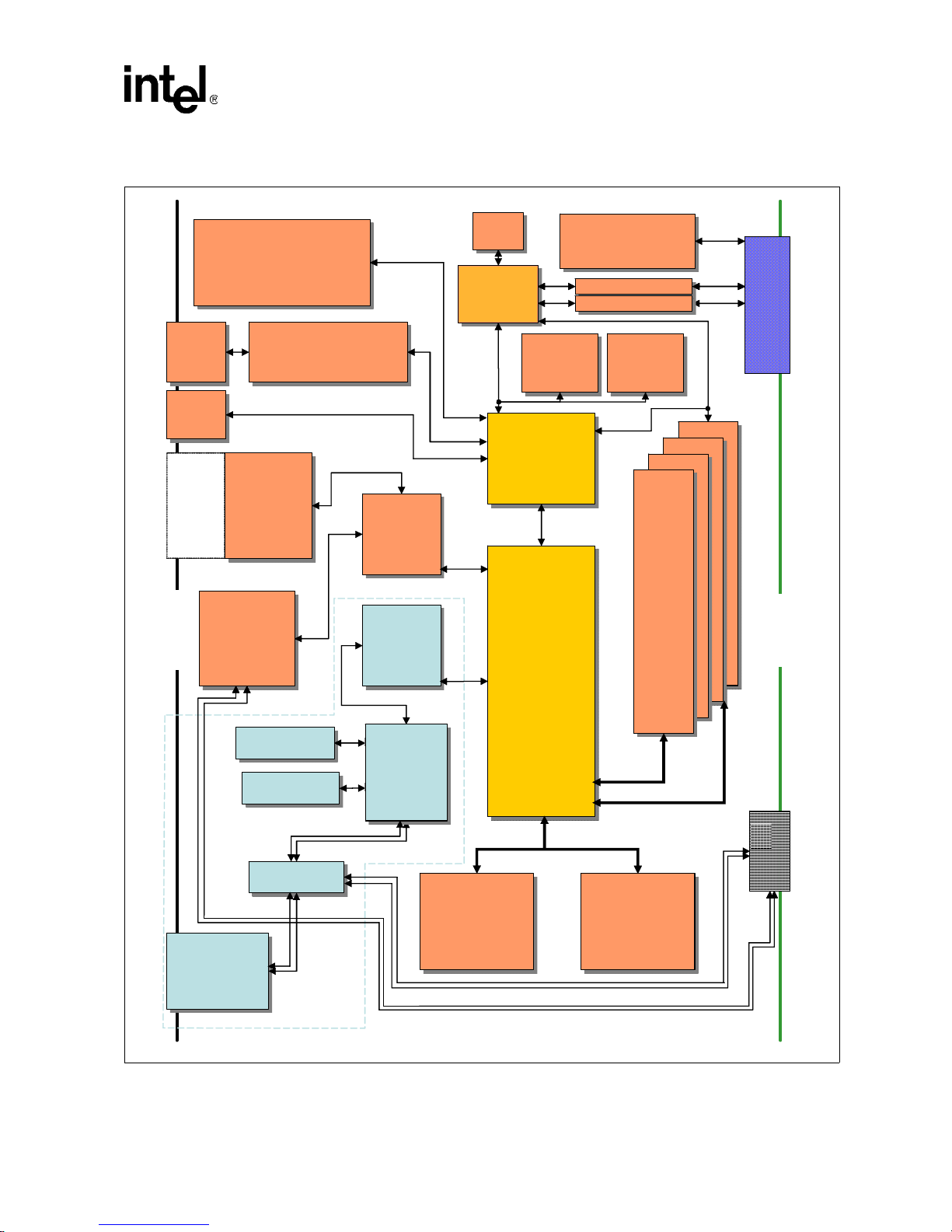
This topic defines the architecture of the MPCBL0001 SBC through descriptions of functional
blocks. Figure 1, “Block Diagram” on page 17 shows the functional blocks of the MPCBL0001
SBC. The MPCBL0001 SBC is a dual processor, hot-swappable SBC with backplane connections
to dual Gigabit Ethernet star networks and dual Fibre Channel star arbitrated loops.
The SBC incorporates an Intelligent Platform Management Controller that monitors critical
functions of the board, responds to commands from the shelf manager, and reports events.
Power is supplied to the MPCBL0001 SBC through two redundant -48 V power supply
connections. Power for on-board hardware management circuitry is provided through a standby
converter on the power mezzanine. This co nverter, along with all the other converters on the power
mezzanine are fed by the diode OR'd -48 V supply from the backplane.
The SBC has provision for the addition of a PMC device and supports 32-bit and 64-bit transfers at
33 MHz and 66 MHz. The SBC also offers one USB and one service terminal interface. An
overview of each block follows.
16 Technical Product Specification
Order #273817
Page 17
Intel NetStructure® MPCBL0001 High Performance Single Board Computer
Figure 1. Block Diagram
Contents
RJ-45
RJ-45
Serial
Serial
Port
Port
USB
USB
Port
Port
Optional
Third-
party
PMC
Front Panel
Optional 2.5”
Optional 2.5”
Hard Disk Drive
Hard Disk Drive
Standard
Microsystems Corp.
Microsystems Corp.
LPC47B272 Super I/O
LPC47B272 Super I/O
PCI
PCI
Mezzanine
Mezzanine
Card
Card
(PMC)
(PMC)
Connector
Connector
Intel®
Intel®
82546EB
82546EB
Dual Gb
Dual Gb
Ethernet
Ethernet
256K SRAM
256K SRAM
256K SRAM
256K SRAM
Dual FC Ports
Standard
528 MB/s
PCI 64/66
1066 MB/s
PCI-X
1066 MB/s
33/66/100
Intel®
Intel®
P64H2
P64H2
PCI
Bridge
Bridge
Intel®
Intel®
P64H2
P64H2
PCI
Bridge
Bridge
PCI-X
QLogic
QLogic
QLogic
QLogic
ISP2312
ISP2312
ISP2312
ISP2312
Fibre
Fibre
Channel
Channel
Channel
Channel
Controller
Controller
Controller
Controller
ATA
PCI
PCI
Fibre
Fibre
ADM
ADM
1026
1026
Sahalee
IPMC
Sahalee
IPMC
IPMC
(4MB/s)
33 MHz
LPC
Intel® ICH3
Intel® ICH3
266 MB/s HI 1.5
1066
MB/s
HI-2
1066
Intel® E7501
Intel® E7501
Intel® E7501
Intel® E7501
Intel® E7501
Intel® E7501
MB/s
HI-2
Controller Hub
Controller Hub
Controller Hub
Controller Hub
Controller Hub
Controller Hub
400MT/s 3.2GB/s
Intel
Intel
82802AC
82802AC
(FWH0)
(FWH0)
Memory
Memory
Memory
Memory
Memory
Memory
(MCH)
(MCH)
(MCH)
(MCH)
(MCH)
(MCH)
On-board Power
On-board Power
Supplies and Hot
Supplies and Hot
Swap Circuitry
Swap Circuitry
IPMB Isolators
IPMB Isolators
IPMB Isolators
IPMB Isolators
IPMB Isolators
IPMB Isolators
IPMB Isolators
IPMB Isolators
Intel
Intel
82802AC
82802AC
(FWH1)
(FWH1)
Four
Four
Four
Four
Four
Four
184-pin
184-pin
184-pin
184-pin
184-pin
184-pin
DIMM
DIMM
DIMM
DIMM
DIMM
DIMM
Sockets
Sockets
Sockets
Sockets
Sockets
Sockets
DDR-266
DDR-266
DDR-266
DDR-266
DDR-266
DDR-266
ECC
ECC
ECC
ECC
ECC
ECC
SDRAM
SDRAM
SDRAM
SDRAM
SDRAM
SDRAM
2.1 GB/s
DDR-266
2.1 GB/s
DDR-266
-48V
IPMB-A
IPMB-B
SMBUS
P10
Backplane
J23
MUX
MUX
Dual FC
Ports
Dual SFP
Dual SFP
Connectors
Connectors
MPCBL0001Fxx
products on ly
Technical Product Specification 17
Order #273817
Low Voltage
Low Voltage
Intel® Xeon™
Intel® Xeon™
Processor
Processor
Low Voltage
Low Voltage
Intel® Xeon™
Intel® Xeon™
Processor
Processor
Dual Fibre Channel Ports to Fabric Interface
Dual Gigabit Ethernet Ports to Base Interface
Page 18

Intel NetStructure® MPCBL0001 High Performance Single Board Computer
Contents
2.2.1 Low Voltage Intel® Xeon
(U36)
The MPCBL0001 SBC supports up to two Low Voltage Intel® Xeon™ processors (see Figure 20,
“Component Layout (#1)” on page 100 for locations). The Low Voltage Xeon processor
incorporates Intel
performance levels that are significantly higher than previous generations of IA-32 family
processors. The processors include the following features:
• 2.0 GHz with a 400 MHz system bus
• 512 Kbyte L2 cache
• Hyper-pipelined technology
• Advanced dynamic execution
• Execution trace cache
• Streaming SIMD (single instruction, multiple data) extensions 2
• Advanced transfer cache
• Enhanced floating point and multimedia engine
• Intel & OEM EEPROM and thermal sensor manageability features
• Supports single and dual processor configurations
• Throttling enabled for protection against high temperatures
®
NetBurst™ microarchitecture and a high-bandwidth Front-Side Bus, allowing
™
Processor CPU-0 (U35), CPU-1
The Low Voltage Xeon processor host bus utilizes a split-transaction, deferred-reply protocol. The
host bus uses source-synchronous transfer of address and data to improve through pu t at the 100 or
133 MHz bus frequency (depending on processor model). Addresses are transferred at 2X the bus
frequency while data is transferred at 4X the bus frequency, resulting in peak data transfer rates up
to 3.2 or 4.3 GBytes/s.
In addition to the NetBurst microarchitecture, the Low Voltage Intel Xeon processor includes a
groundbreaking technology called Hyper-Threading Technology
Technology improves processor performance for multithreaded applications or multitasking
environments by supporting multiple software threads on each processor.
Low Voltage Intel Xeon processors require their package case temperatures to be operated below
an absolute maximum specification. If the chassis ambient temperature exceeds a level whereby
the processor thermal cooling subsys tem can no longer maintain the specified case temperature, th e
processors will automatically enter a mode called Thermal Monitor to reduce their case
temperatures. Thermal Monitor controls the processor temperature by modulating the internal
processor core clocks, thereby reducing internal power dissipation, and does not require any
interaction by the Operating System or Application. Once the case temperatures have reached a
safe operating level, the processor will return to its non-modulated operating frequency. See the
Low Voltage Intel Xeon processor datasheet, referenced in Appendix A, “Reference Documents”,
for further details.
An optional ITP700 port connection is included to facilitate debug and BIOS/software
development efforts. This JTAG connection to the processors utilizes voltage-signaling levels that
are specific to the Low Voltage Xeon processor family. These levels must not be exceeded or
processor damage may occur. Please refer to Intel document ITP700 Debug Port Design Guide,
order number 249679-005 for additional information on the ITP connector pin definitions.
†
(HT Technology). HT
18 Technical Product Specification
Order #273817
Page 19

Intel NetStructure® MPCBL0001 High Performance Single Board Computer
2.2.2 Chipset
The Intel® E7501 chipset consists of three major components:
®
• Intel
• Intel
• Intel
See Figure 20, “Component Layout (#1)” on page 100 for their locations.
2.2.2.1 Intel® E7501 Memory Controller Hub (U22)
The Intel® E7501 Memory Controller Hub (MCH) interfaces between the processor system bus
and the memory and I/O subsystems.
Significant features are listed below:
• System/host bus features:
E7501 Memory Controller Hub (MCH)
®
82801CA I/O Controller Hub 3 (ICH3)
®
82870P2 64-bit PCI/PCI-X Controller Hub 2 (P64H2)
— Supports dual processors at either 400 or 533 MT/s or a bandwidth of 3.2 or 4.3 GBytes/s
— Supports a 36-bit system bus addressing model
Contents
— 12 deep in-order queue, two deep defer queue
Note: The current MPCBL0001 is designed to run with the Intel
processor frequency, the processor side bus (PSB) will run at 400 MT/s with a bandwidth of 3.2
GBytes/s.
• Memory subsystem features:
— 144-bit wide (72-bit x 2), DDR-266 memory interfaces with 3.2 or 4.3 GByte/s bandwidth
— Supports x72, registered DDR-266 ECC DIMMs using 64-, 128-, 256-, and 512-Mbit
SDRAMs
— Supports a maximum of 16 GBytes of memory (MPCBL0001 SBC implementation
supports a maximum of 8 Gbytes).
— Supports S4EC/D4ED ChipKill* ECC (x4 ChipKill)
• Corrects all bit errors within a single 4-bit nibble
• Detects all errors contained within two 4-bit nibbles
• Memory scrubbing supported
— Supports up to 32 simultaneous open pages
— Hardware support for auto-initialization of memory with valid ECC
• I/O features:
— Hub interface A provides HI 1.5 connection for ICH3
• 266 MB/s data bandwidth with parity protection
• 8 bits wide, 66 MHz clock, 4x data transfer (quad-pumped)
• Supports 64-bit inbound addressing, 32-bit outbound addressing
®
LV Xeon® 2.0 GHz processor . At this
— Hub interfaces B and C provide HI2.0 connections for two P64H2s
• 1 GByte/s data bandwidth with ECC protection in each direction
Technical Product Specification 19
Order #273817
Page 20

Intel NetStructure® MPCBL0001 High Performance Single Board Computer
Contents
• 16-bits wide, 66 MHz clock, 8x data transfer (octal pumped)
• Supports 64-bit inbound, 32-bit outbound addressing
The MCH I/O subsystems interface incorporates four hub inter faces. Each Hu b interf ace is a poin tto-point connection between the MCH and an I/O bridge/device. The various components of the
chipset communicate via these connected hub interfaces:
• The first hub link connects the MCH to the ICH3.
• The next two hub link interfaces connect the MCH to P64H2 components.
• The remaining hub link is unused.
2.2.2.2 Intel® 82801CA I/O Controller Hub 3 (U7)
The Intel® 82801CA I/O Controller Hub 3 (IHC3) provides the legacy I/O subsystem and
integrates advanced I/O functions. ICH3 features are listed below:
• IDE interface controller
• Three Universal Host Controller Interface (UHCI)
• USB host controllers supporting up to 6 ports (MPCBL0001 SBC implementation supports
one port on the front panel)
• Integrated I/O APIC
• SMBus 2.0 controller
• LPC interface
• Watchdog timer #3 (see “Watchdog Timers (WDTs)” on page 64)
• PCI 2.2 bus interface supporting 32bit/33 MHz operation
• Connects to MCH through Hub Interface A (HI 1.5)
The MPCBL0001 SBC implements one USB port and does not use the ICH3 PCI connection.
2.2.2.2.1 PCI Bus Master IDE Interface (J24)
The ICH3 acts as a PCI based, enhanced IDE, 32-bit interface controller for intelligent disk drives
that have disk controller electronics onboard. The SBC includes a single 40-pin (2 x 20) IDE
connector (J24) that supports one master or one slave device. See Figure 20, “Component Layout
(#1)” on page 100 drawing for its location. The IDE controller provides support for an internally
mounted 2. 5” hard disk. The IDE co ntroller has the follow ing features:
• PIO and DMA transfer modes
• Mode 4 timings
• Supports Ultra ATA33/66/100 synchronous DMA
• Buffering for PCI/IDE burst transfers
• Master/slave IDE mode
• Support for up to two devices (Master/Slave) via a single primary IDE connector
(MPCBL0001 SBC implementation supports one optional physical 2.5" IDE device)
Note: Incorporating an optional IDE Hard Disk drive may significantly impact the Reliability
Specifications in Section 6.3.
Note: Performance of the IDE interface may be impacted by the DMA mode and type of DMA transfers
20 Technical Product Specification
Order #273817
Page 21

Intel NetStructure® MPCBL0001 High Performance Single Board Computer
used. Even though the B IOS automatically s ets the DMA mode/type, the OS could downgrade the
DMA transfer mode. Check the operating system documentation to see what DMA mode is used
by default and whether it is possible to change to a higher performance DMA mode.
2.2.2.3 Intel® 82870P2 64-bit PCI/PCI-X Controller Hub 2 (U14, U24)
The two P64H2 devices provide the system’s high-performance PCI bus support. See Figure 20,
“Component Layout (#1)” on page 100 for their locations. Each P64H2 component supports two
independent, 64-bit, PCI/PCI-X interfaces. 32-bit/33 MHz and 64-bit/66 MHz PCI bus modes are
also supported. Each PCI bus interface features:
• PCI-X 1.0 Specification compliance
• PCI Specification 2.2 compliance
• PCI-PCI Bridge Rev 1.1 compliance
• PCI Hot Plug 1.0 compliance
• I/O APIC supporting up to 24 interrupts (16 external pins)
• PCI peer-to-peer write capability between PCI ports
• SMBus target for Out-of-Band access to all internal PCI registers
Contents
Each of the two P64H2 devices (U14, U2 4) included on the MPCBL00 01 SBC pro vides t he bridge
to two independent PCI bus connections, as shown in Table 1, “P64H2 Interfaces” on page 21.
T able 1. P64H2 Interfaces
P64H2 Device Interface
U24 PCI-X interface to the optional dual Fibre Channel controller
U14
The two high-speed communications interfaces ( Gigabit Ethernet and Fibre Ch annel) are located in
separate P64H2 devices to maximize data throughput. A single HI-2 hub link connection from the
P64H2 to the MCH provides a >1 Gbyte/s bandwidth back to memory and the processor System
Bus.
• PCI-X interface to the dual Gigabit Ethernet controller
• 64-bit/66 MHz PCI bus for a plug-in PMC card
2.2.3 Memory (J8, J9, J10, J11)
Four DDR 266 DIMM sockets make up the memory subsystem. See Figure 20, “Component
Layout (#1)” on page 100 for their locations. The MCH defines two memory channels operating in
parallel to logically create a 144-bit wide memory data path. ECC is generated and checked across
128 bits of data, allowing for significant improvement in error correction.
Due to this architecture, DDR DIMMs must be installed in matched pairs. Memory DIMM
configurations ranging from 512 MBytes to 8 GBytes in 512 MByte increments are supported.
2.2.3.1 Memory Ordering Rule for the MCH
Platforms based on the E7501 chipset require DDR DIMMs to be populated in matched pairs in a
specific order. Start with the two DIMMs furthest from the MCH in a “fill-farthest” approach (see
Figure 2). This requirement is based on the signal integrity requirements of the DDR interface.
Technical Product Specification 21
Order #273817
Page 22
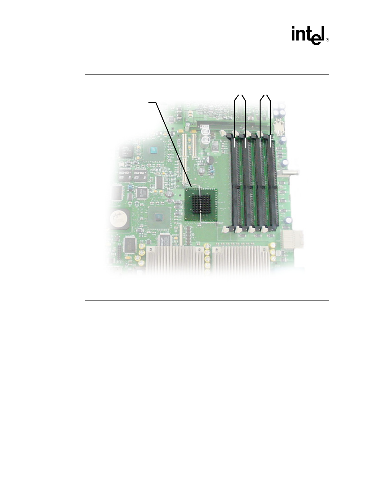
Intel NetStructure® MPCBL0001 High Performance Single Board Computer
Contents
Figure 2. Memory Ordering
MCH, U22
J8
Fill
Last
J9
Fill
First
J11
J10
B0894-01
2.2.4 I/O
2.2.4.1 Super I/O (U28)
The Super I/O device (SIO) is an SMSC LPC47B272 enhanced Super I/O controller. The SIO
connects to the ICH3 th rough its LPC b us connect ion. Th e SIO provides suppor t fo r th e front panel
serial port (J17, see page 80). There is no front-panel connection to the legacy keyboard and mouse
PS/2 ports. Keyboard and mouse support are provided by the USB connection (J12, see page 87).
See Figure 13 for connector locations.
To facilitate debug and BIOS development, SIO connections such as legacy (PS/2) keyboard/
mouse and floppy may be provided on initial board revisions. Software must not rely on the
presence of these connections on future board revisions.
22 Technical Product Specification
Order #273817
Page 23

Intel NetStructure® MPCBL0001 High Performance Single Board Computer
2.2.4.2 Real-Time Clock
The MPCBL0001 SBC real-time clock is integrated into the ICH3. It is derived from a 32.768 KHz
crystal with the following specifications:
• Frequency tolerance @ 25 ºC: ±20ppm
• Frequency stability: maximum of -0.04ppm/(ΔºC)
• Aging ΔF/f (1
st
year @ 25 ºC): ±3ppm
• ±20ppm from 0-55 ºC and aging 1ppm/year
The real-time clock is powered by a 0.22F SuperCap* capacitor when main power is not applied to
the board. This capacitor powers the real-time clock for a minimum of two hours while external
power is removed from the MPCBL0001 SBC.
See Section 3.13, “Watchdog Timers (WDTs)” on page 64 for information about the real-time
clock timers.
2.2.4.3 Timer0 Capabilities
Timer0, integrated inside the ICH3, is an 8254 compatible timer. This timer is set up to generate a
periodic waveform that creates the edge for the timer0 interrupt. The interrupt is received by the
ICH3 APIC and communicated to the CPU(s).
Contents
2
MPCBL0001 provides a high-precision 14.318 MHz crystal clock source as the reference for the
timer0 counters. To improve timing accuracy, the crystal used is a low-PPM, high-stability
component with the following specifications:
• Frequency tolerance (25º C): ±10ppm
• Temperature characteristics (-10º C to +60º C): ±5ppm
• Aging: ±1pp m per year max
This timer does not operate when board power is removed.
2.2.4.4 Gigabit Et hernet (U13 )
The MPCBL0001 SBC implements two Gigabit Ethernet interfaces, each of which is routed to the
fabric/switch slot through the backplane (J23, see page 85). There are no direct, external Ethernet
ports included on the SBC board. Each Ethernet connection utilizes an 82546 Dual Gigabit
Ethernet Controller, allowing support for 1000Mbits/s, 100Mbits/s and 10Mbits/s data rates.
The 82546 controller is optimized for designs using the PCI and the emerg ing PCI-X bus interface
extension. The MPCBL0001 SBC has a 133 MHz PCI-X bus connection. The integrated physical
layer circuitry (PHY) provides an IEEE 802.3 Ethernet Interface for 1000Base-T, 100Base-TX,
and 10Base-T applications.
Features include:
• 32/64-bit 33/66 MHz, PCI Rev 2.2 compliant interface
• Host interface also compliant with the PCI-X addendum, Rev 1.0a, from 50 to 133 MHz
• Supports 64-bit addressing
• Efficient PCI bus master operation, supported by optimized internal DMA controller
Technical Product Specification 23
Order #273817
Page 24

Intel NetStructure® MPCBL0001 High Performance Single Board Computer
Contents
• Supports advanced PCI commands such as MWI, MRM, and MRL, and PCI-X commands
such as MRD, MRB, and MWB
• Full IEEE 802.3ab auto-negotiation of speed, duplex, and flow-control configuration
• Complete full duplex and half duplex support
• Automatic MDI crossover operation for 100Base-TX and 10Base-T modes
• Automatic polarity correction
• Digital implementation of adaptive equalizer and canceller for echo and crosstalk
2.2.4.5 Fibre Channel* (U23) - Optional
The QLogic* ISP2312 dual Fibre Channel controller is used for access to high-speed storage
subsystems. It is routed through backplane connector P23.
See Figure 20, “Component Layout (#1)” on page 100 for its location.
This controller supports PCI and PCI-X bus interfaces. Burst mode master DMA transfers are
utilized for efficient usage of bus bandwidth during data transfers, and 8, 16, and 32-bit accesses
are supported as a PCI target. The controller appears as two independent Fibre Channel ports. A
PCI function is assigned to each port in the device’s PC I conf iguration s pace. Func tions 0 and 1 are
used to configure FC ports 1 and 2, respectively.
ISP2312 features include:
• 32/64-bit 33/66 MHz, PCI Rev 2.2 compliant interface.
• Host interface compliant with the PCI-X addendum, Rev 1.0a, from 50 to 133 MHz.
• Supports 64-bit addressing (addresses >32 bit initiate use of DAC address cycle).
• Efficient PCI bus master operation, supported by optimized internal DMA controller.
• Supports advanced PCI commands such as MWI, MRM, and MRL, and PCI-X commands
such as MRD, MRB, and MWB.
• Automatically negotiates Fibre Channel bit rate 1.06 Gbits/s (through backplane or front
panel) or 2.12 Gbits/s (through front-panel Fibre Channel ports only)
• Supports up to 533 MBytes sustained FC data transfer rate (combined bandwidth of both
directions transmitting simultaneously).
• Supports Fibre Channel-arbitrated loop (FC-AL), FC-AL-2, point-to-point, and switched
fabric topologies.
• Maxim MAX3840 2x2 crosspoint switch for switching Fibre Channel between the front ports
and the backplane, either via the BIOS Setup Menu by electronic keying.
• Each FC port includes:
— Internal RISC processor
— Receive DMA sequencer
— Frame buffer
— DMA channels (transmit, receive, command, auto-request, and auto-response)
24 Technical Product Specification
Order #273817
Page 25

Intel NetStructure® MPCBL0001 High Performance Single Board Computer
• Support for JTAG boundary scan.
• Supports IP as well as other protocols; however there are currently no plans to validate
protocols other than SCSI_FCP.
Each Fibre Channel interface of the ISP2312 includes its own internal 16-bit RISC processor and
external 7.5 ns synchronous SRAM memory for instruction code and data. Parity protection is
provided on accesses to this memory. The SBC utilizes two 256 KByte (128Kx18) SRAMs, one for
each port, for the ISP2312 memory requirements.
An external 256 x 16 non-volatile EEPROM is used to store system configuration parameters and
PCI subsyst em and subsystem vendor IDs. The first 128 bytes are used for function 0 parameters
and the second 128 bytes are used for function 1.
2.2.5 PMC Connector (J25, J26, J27)
The MPCBL0001 SBC supports one 64-bit, 66 MHz PMC slot. The PMC slot is connected to the
second of two P64H2 hub controllers via PMC Connectors J25-J27. The PMC slot has an opening
in the front panel of the SBC that exposes the I/O connectors of the add-in PMC card. PMC cards
can only be added to or removed from this slot when the board is outside the system chassis. See
Figure 20, “Component Layout (#1)” on page100 for its location.
Contents
The PCI bus specification provides the means for backward compatibility with slower PMC cards
(32-bit or 33 MHz) through the use of the M66EN pin. A PMC card that does not support 66 MHz
operation grounds the M66EN pin when installed to inform the SBC hardware to provide a 33
MHz clock to this interface. Support for 32-bit only PMC cards is accomplished through the use of
the REQ64#/ACK64# PCI bus protocol.
The PMC slot provided by the SBC connects the PCI VI/O voltage pins to +3.3 V. This requires
use of PMC plug-in cards that support +3.3 V I/O signal levels. Only PMC plug-in cards
designated “+3.3 V only” or “universal” voltage I/O are supported. The PMC plug-in location
provides a key pin to prevent insertion of cards that do not meet this requirement. Note that +5 V
power is still supplied to the PMC pins designated for +5 V connections. The PMC is allotted 1.5 A
of current.
2.2.6 Firmware Hub (U30, U33)
The MPCBL0001 SBC supports two 8Mbit (1 MByte) BIOS flash ROMs:
• Primary BIOS flash ROM (FWH0)
• Recovery BIOS flash ROM (FWH1)
The flash is allocated for BIOS and Firmware usage.
The SBC boots from the primary flash ROM under n ormal circums tances. During t he boot process ,
if the BIOS (or IPMC) determines that the contents of the primary flash ROM are corrupted, a
hardware mechanism is available to change the flash device select logic to the recovery flash
ROM. See Section 2.2.6.3, “Flash ROM Backup Mechanism” on page 26 for more information.
Each flash component has a separately write-protected boot block that prevents erasure when the
device is upgraded.
Technical Product Specification 25
Order #273817
Page 26

Intel NetStructure® MPCBL0001 High Performance Single Board Computer
Contents
Flash ROM BIOS updates can be performed by an end user or a network administrator over the
LAN. The system should complete booting to an OS, MS-DOS* or logon to Linux* as root user.
The system should have a local copy of the flash program and the BIOS data files or have the
capability to copy the flash program and BIOS data files onto a local drive via the network. The
flash program has a command line interface to specify the path and the file name of the BIOS data
files. After completing the BIOS ROM update the user should shutdown and reset the system to let
the new BIOS ROM take effect. See Section 7.7, “BIOS Updates” on page 112 for more
information.
2.2.6.1 FWH 0 (Main BIOS)
BIOS execute code off this flash and perform checksum validation of its operational code. This
checksum occurs in the boot block of the BIOS. The BIOS image is also stored in FWH0. When
user performs BIOS update, the BIOS image will be stored in FWH 0 only. FWH0 will also store
the factory default CMOS settings user configured CMOS settings.
1. When user "Load optimal defaults" from the BIOS setup screen, it restores the factory default
by copying the "Factory Default" settings from FWH0 to ICH3 (CMOS).
2. When user "Save custom defaults" from the BIOS setup screen, the changes will be made to
the CMOS settings on ICH3 and then copied from ICH3 to FWH0.
3. When user "Load custom defaults" from the BIOS setup screen, the "custom" CMOS settings
are copied from FWH0 to ICH3.
2.2.6.2 FWH 1 (Backup/Recovery BIOS)
FWH 1 stores the recovery BIOS. In the event of checksum failure on the Main BIOS operational
code, BIOS will request BMC to switch FWH, so that the board will be able to boot up from FWH1
for recovery.
User is able to boot up the board from FWH1 by executing an OEM IPMI command as well (see
Section 3.7.1, “Reset BIOS Flash Type” on page49).
2.2.6.3 Flash ROM Backup Mechanism
The on-board Intelligent Platform Management Controller (IPMC) manages which of the two
BIOS flash ROMs is used during the boot process. The IPMC monitors the boot progress and can
change the flash ROM selection and reset the processor.
The default state of this control configures the primary Firmware Hub (FWH) ROM device ID to
be the boot device; the secondary FWH is assigned the next ID. The secondary FWH responds to
the address range just below the primary FWH ROM in high memory.
The Intelligent Platform Management Controller sets the ID for both FWH devices. Boot accesses
are directed to the FWH with ID = 0; unconnected ID pins are pulled low by the FWH device. In
this way the IPMC may select which flash ROM is used for the boot process.
Refer to Section 3.7.1, “Reset BIOS Flash Type” on page 49 for a descript ion of how to do this
manually.
26 Technical Product Specification
Order #273817
Page 27

Intel NetStructure® MPCBL0001 High Performance Single Board Computer
2.2.7 Onboard Power Supplies
The main power supply rails on the MPCBL0001 SBC are powered from dual-redundant -48 V
power supply inputs from the backplane power connector (P10). There are also dual redundant,
limited current, make-last-break-first (MLBF) power connections. See Figure 20, “Component
Layout (#1)” on page 100 for their location.
2.2.7.1 Power Feed Fuses
As required by the PICMG 3.0 Specification, the MPCBL0001 SBC provides fuses on each of the
-48V power feeds and on the RTN connections as well. The fuses on the return feeds are critical to
prevent overcurrent situations if an ORing diode in the return path fails and there is a voltage
potential difference between the A and B return paths.
2.2.7.2 ORing Diodes and Circuit Breaker Protection
The two -48 V power connectors are OR’d together. A current limiting FET switch is co nnected
between the OR’d -48 V and the primary DC-DC converters. The FET switch provides three
functions:
• A mechanism to electrically connect/disconnect the SBC to/from the two -48 V inputs.
• A soft-on function.
Contents
• An over-current circuit breaker feature.
2.2.7.3 -48 V to +12 V Converter
This converter provides DC isolation between the -48 V and -48 V return connections and all of the
derived DC power on the MPCBL0001 SBC. Its output is connected to the SBC’s +12 V power
rail. The converter supplies a maximum of 9 A of current. The converter is enabled/disabled by the
onboard IPMC.
2.2.7.4 -48 V to +5 V/+3.3 V Converter
This converter provides DC isolation between the -48 V and -48 V return connections and all of the
derived DC power on the MPCBL0001 SBC. Its output is connected to the SBC’s +5 V and 3.3 V
power rails. The converter supplies a maximum of 9 A of +5 V current and 9 A of +3.3 V current.
The converter is enabled/disabled by the onboard IPMC.
2.2.7.5 Processor Voltage Regulator Module (VRM)
The Voltage Regulator Module (VRM) provides core power to the two Low Voltage Xeon
processors. The input to the VRM is connected to the +12 V power rail.
See Figure 20, “Component Layout (#1)” on page 100 for its location.
Technical Product Specification 27
Order #273817
Page 28

Intel NetStructure® MPCBL0001 High Performance Single Board Computer
Contents
The VRM controller is designed to support multiple processor core voltages selected by the voltage
identification (VID) pins on the pro cessor. Logic provided on the SBC ensu res that th e VRM is not
enabled if the two processors request different VID codes. In addition, the VRM is disabled until
all other voltage converters indicate “power good.” The voltage regulator module is designed to
support up to two 43 W (TDP - Thermal Design Power) processors.
Note: The +5 VSB power rail only needs to supply at least 4.0 V to properly power any circuitry that uses
the +5 VSB rail when the payl oad power (i.e., processo rs, ethernet controller, etc.) is not turned on.
Any alerts from the +5 VSB sensor when the system is not in the M4, M5, or M6 states should be
ignored.
2.2.7.6 IPMB Standby Power
This converter provides DC isolation between the -48 V and -48 V return connections and all of the
derived DC power on the MPCBL0001. Its output is connected to the IPMB and standby +5 V
power rail of the SBC. The converter supplies a maximum of 1.5 A of +5 V current. A +3.3 V
management voltage is derived from the IPMB power by means of a linear regulator circuit and is
used to power most of the IPMC functions. Standby power is derived from the -48 V rails and is
always available on the SBC unless the overall system power rail (-48 V) is shut down.
28 Technical Product Specification
Order #273817
Page 29
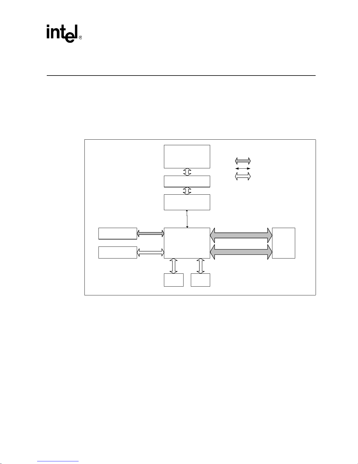
Intel NetStructure® MPCBL0001 High Performance Single Board Computer
Contents
Hardware Management Overview 3
The Intelligent Platform Management Controller (IPMC) is an Intel-designed baseboard
management controller device manufactured by Philips Semiconductor* for Intel.
The high-level architecture of the baseboard management for MPCBL0001 is represented in the
block diagram below.
Figure 3. Hardware Management Block Diagram
ADM 1026
Wat chdog Tim er
CPU
(Low Voltage Int el
Xeon™)
Intel® E7501 Memory
Cont roller Hub (MCH)
ICH3
Intelligent Platf orm
Management C ontroller
(IPMC)
Flash
Mem ory
SRAM
®
NOTE:
IPMB A
I
M
P
B
B
I2C Bus
KCS interface
Logic C onnect ion
Backplane
(P10)
The main processors communicate with the IPMC using the Keyboard Controller Style (KCS)
interface. Two KCS interfaces are available for the BIOS to communicate to the IPMC. BIOS uses
SMS interface for normal communication and SMM interface when executing code und er s ys tems
management mode (SMM). The base address of the LPC interface for SMS is 0xCA2 and 0xCA4
for SMM operation. Besides that, the BIOS is able to communicate with the IPMC for POST error
logging purposes, fault resilient purposes, and critical interrupts via the KCS interface.
The memory subsystem of the IPMC consists of a flash memory to hold the IPMC operation code,
firmware update code, system event log (SEL), and a sensor data record (SDR) rep ository. RAM is
used for data and occasionally as a storage area for code when flash programming is under
execution. The field replacement unit (FRU) inventory information is stored in the nonvolatile
memory on ADM1026. The flash memory can store up to 64 KBytes of SEL events and SDR
information, while the ADM1026 can store up to 512 bytes of FRU information. Having the SEL
and logging functions managed by the IPMC helps ensure that ‘post-mortem’ logging information
is available even if the system processor becomes disabled.
Technical Product Specification 29
Order #273817
Page 30

Intel NetStructure® MPCBL0001 High Performance Single Board Computer
Contents
The IPMC provides six I2C bus connections. Two are used as the redundant IPMB bu s conn ections
to the backplane while another one is used for communication with the ADM1026. The remaining
buses are unused. If an IPMB bus fault or IPMC failure occurs, IPMB isolators are used to switch
and isolate the backplane/system IPMB bus from the faulted SBC board. Where possible, the
IPMC activates the redundant IPMB bus to re-establish system management communication to
report the fault.
The onboard DC voltages are monitored by the ADM1026 device, manufactured by Analog
Devices. The IPMC queries the ADM1026 over a local system management I
ADM1026 includes voltage threshol d setting s that can be co nfigured to gene rate an interr upt to t he
IPMC if any of the thresholds are exceeded.
To increase the reliability of the MPCBL0001 SBC, a watchdog timer is implemented, whereby it
strobes an external watchdog timer at two-second intervals to ensure continuity of operation of the
board’s management subsystem. If the IPMC ceases to strobe the watchdog timer, the watchdog
timer isolates the IPMC from the IPMBs and resets the IPMC. The watchdog timer exp ires after six
seconds if strobes are not generat ed , and i t res et s the IP MC. D etail ed i n form atio n on the w atch dog
timer configuration can be queried using standard IPMI v1.5 watchdog timer commands. The
watchdog timer does not reset the payload power.
3.1 Sensor Data Record (SDR)
Sensor Data Records contain information about the type and number of se nsors in the baseboard,
sensor threshold support, event generation capabilities, and the types of sensor readings handled by
system management firmware.
The MPCBL0001 management controller is set up as a satellite management controller (SMC). It
does support sensor devices, whose population is static by nature. SDRs can be queried using
Device SDR commands to the firmware. Refer to Section B, “List of Supported Commands (IPMI
v1.5 and PICM G 3.0)” on page 189 for the list of supported IPMI commands for SDRs. Hardware
sensors that have been implemented are listed below.
Table 2. Hardware Sensors (Sheet 1 of 3)
2
C bus. The
Sensor
Number
01h Power Unit Payload Power IPMC Power On Soft power control
03h Watchdog Timer IPMC Watchdog
06h System Firmware
07h CPU Critical
08h Memory Error ECC Multiple Bit
Sensor Type
Progress
Interrupt
Voltage/Signals
Monitored
Timer timeout
PCI SERR IPMC Power On PCI SERR signal
PCI PERR IPMC Power On PCI PERR signal
error
ECC Single Bit error IPMC Power On No change
Monitored
via
IPMC Power On/
IPMC Power On No change
IPMC Power On Multiple Bit Error or
Scanning
Enabled
under Power
State
Off
Health LED
(Green to Red)
failure (Offset Bit 05h
asserted
No change
asserted
asserted
Uncorrectable ECC
occurred
30 Technical Product Specification
Order #273817
Page 31

Intel NetStructure® MPCBL0001 High Performance Single Board Computer
Table 2. Hardware Sensors (Sheet 2 of 3)
Contents
Sensor
Number
Sensor Type
09h Event Logging
Disabled
Voltage/Signals
Monitored
BIOS Generated
events
Monitored
via
BIOS SMI Power On No change
10h Voltage 3.3 VSB ADM 1026 Power On/
11h Voltage +5 VSB ADM 1026 Power On/
12h +1.8 VSB ADM 1026 Power On/
13h V BAT ADM 1026 Power On/
Scanning
Enabled
under Power
State
Off
Off
Off
Off
Health LED
(Green to Red)
Exceeds critical
threshold
Exceeds critical
threshold
Exceeds critical
threshold
Exceeds critical
threshold
14h +1.2 V ADM 1026 Power On Exceeds critical
threshold
15h VTT DDR (+1.25 V) ADM 1026 Power On Exceeds critical
threshold
16h +1.8 V ADM 1026 Power On Exceeds critical
threshold
17h +2.5 V ADM 1026 Power On Exceeds critical
threshold
18h +3.3 V ADM 1026 Power On Exceeds critical
threshold
19h +5 V ADM 1026 Power On Exceeds critical
threshold
30h Temperature Board Temperature ADM 1026 Power On/
Off
Exceeds critical
threshold
37h CPU 0 Temperature ADM 1026 Power On Exceeds critical
threshold
38h CPU 1 Temperature ADM 1026 Power On Exceeds critical
threshold
50h Processor CPU 0 Presence ADM 1026 Power On/
IERR signal asserted
Off
50h CPU 0 IERR IPMC Power On No change
50h CPU 0 Thermtrip IPMC Power On ThermTrip signal
asserted
50h CPU 0 Non-
Presence
51h CPU 1 Presence ADM 1026 Power On/
ADM 1026 Power On/
Off
CPU 0 is detected as
missing
IERR signal asserted
Off
51h CPU 1 IERR IPMC Power On No change
51h CPU 1 Thermtrip IPMC Power On ThermTrip signal
asserted
54h Boot Error BIOS Main Flash IPMC Power On No change
55h BIOS FRED Flash IPMC Power On No change
56h CPU 0 ProcHot
57h CPU1 ProcHot
1
IPMC Power On ProcHot signal asserted
1
IPMC Power On ProcHot signal asserted
Technical Product Specification 31
Order #273817
Page 32

Intel NetStructure® MPCBL0001 High Performance Single Board Computer
Contents
Table 2. Hardware Sensors (Sheet 3 of 3)
Sensor
Number
82h ACPI State ACPI State IPMC Power On/
83h System Event System Event IPMC Power On No change
1Ah +12 V ADM 1026 Power On Exceeds critical
1Bh -12 V ADM 1026 Power On Exceeds critical
1Ch CPU Core Voltage ADM 1026 Power On Exceeds critical
1Dh Voltage +1.5 V ADM 1026 Power On Exceeds critical
8Ah FRU Hot Swap FRU State IPMC Power On/
8Bh IPMB Link Sensor Operational state of
E0h SMI Timeout Steady state
NOTE: The PROCHOT signal is a discrete signal but it is treated as a threshold sensor so that it can have a
Sensor Type
Sensor Type of Temperature. IPMI does not have a discrete sensor type for temperatures. The
advantage of the PROCHOT sensor acting as a temperature sensor is that the CMM can recognize
events from this sensor as temperature events and adjust fan speed accordingly.
Voltage/Signals
Monitored
IPMB-0
assertion of the SMI
line
Monitored
via
Logical Power On/
IPMC Power On SMI Line asserted
Scanning
Enabled
under Power
State
Off
Off
Off
Health LED
(Green to Red)
No change
threshold
threshold
threshold
threshold
No change
No change
(Offset bit 01h asserted)
3.2 System Event Log (SEL)
The SEL is the collection of events that are generated by the IPMC. Event logs are stored in nonvolatile memory. This resides on the board and allows better tracking of error conditions on the
baseboard when it is moved from chassis to chassis. Having the SEL and logging functions
managed by the IPMC helps ensure that post-mortem logging information is available should a
failure occur that disables the systems processor(s). In the MPCBL0001, flash memory for IPMI
firmware can store up to 3276 SEL entri es. Manag e ment s oft ware running on the host processor is
responsible for ensuring that SEL storage has sufficient space for SEL logging. Events are
normally forwarded to shelf manag er and l o gged to SEL on the board. If SEL storage on the board
is full, new events are forwarded to the Shelf Manager but are not logged in to SEL on the board.
A set of IPMI commands (see Tabl e 108, “IPMI 1.5 Supported Commands” on page 189) allows
the SEL to be read and cleared and allows events to be added to the SEL. The IPMI commands
used for adding events to the SEL are Platform Event Message, Add SEL entry, and Partial Add
Entry. Table 3, “SEL Events Supported by the MPCBL0001 SBC” on page 33 lists supported SEL
events. Event Messages can be sent to the IPMC via the IPMB. This provides the mechanism for
satellite controllers to detect events and log them into the SEL.
32 Technical Product Specification
Order #273817
Page 33

Intel NetStructure® MPCBL0001 High Performance Single Board Computer
Table 3. SEL Events Supported by the MPCBL0001 SBC (Sheet 1 of 4)
Contents
Sensor
Type
Reserved 00h - Reserved -
Temperature 01h - Temperature Threshold exceeded for upper critical, upper non-
Voltage 02h - Voltage Voltage exceeded upper critical, upper non-critical,
Processor 07h 00h IERR Processor IERR has occurred.
Power Unit 01h 00h Power Off/Power On Normal power off indication. Offset 0 is just a status
Memory 0Ch 00h Correctable ECC Event data 3 = DIMM pair number
NOTE:
1. These sensor offsets do not generate events, but they are valid offsets when reading the sensor values.
2. Watchdog sensor refers to WDT#1 per Section 3.13.1.
Sensor
Type Code
Sensor-Specific
Offset (Event
Data 1, Bit 0-3)
01h Thermal Trip Processor thermal trip has occurred.
04h FRB3/Processor Startup/
Initialization Failure
(CPU did not start)
05h Configuration Error CPU 0 and CPU 1 are not present.
07h Processor Presence
Detected
09h Terminator Presence
Detected
05h Soft Power Control
Failure (unit did not
respond to request to
turn on)
01h Uncorrectable ECC Event data 3 = DIMM pair number
Event Remarks
critical, lower critical and lower non-critical
thresholds. Refer to Table 4, “Sensor Thresholds for
IPMC Firmware 1.0” on page 37 for sensor
thresholds data.
lower critical and lower non-critical thresholds. Refer
to Table 4 for sensor thresholds data.
An FRB3 Timer (30 seconds) was implemented to
detect the failure of the CPUs from booting.
Event data 3 = Last Post 80 code byte
1
1
indicating that the payload power is off. It does not
generate an event when it is set. (For internal use).
The Power Unit sensor is used to detect when the
Payload power does not come up when the board is
told to power on.
When the board enters M4 state, the IPMC asserts a
Power Enable line to cause the Payload to power up.
The IPMC then waits for another line that indicates
that the power has come up successfully. If that line
does not assert within 2 seconds, then offset 05h is
asserted on the Power Unit sensor, which generates
an event to notify the Shelf Manager of the failure.
00 refers to J8/J9
01 refers to J10/J11
00 refers to J8/J9
01 refers to J10/J11
Technical Product Specification 33
Order #273817
Page 34

Intel NetStructure® MPCBL0001 High Performance Single Board Computer
Contents
Table 3. SEL Events Supported by the MPCBL0001 SBC (Sheet 2 of 4)
Sensor
Type
System
Firmware
Progress
Event
Logging
Disabled
NOTE:
1. These sensor offsets do not generate events, but they are valid offsets when reading the sensor values.
2. Watchdog sensor refers to WDT#1 per Section 3.13.1.
Sensor
Type Code
0Fh 00h BIOS checksum error Event data 2 = 99h
10h 00h Correctable Memory
Sensor-Specific
Offset (Event
Data 1, Bit 0-3)
Event Remarks
Event data 3 = 99h
Timer Count Read/Write
error
CMOS Battery error Event data 2 = FEh
CMOS Diagnosis status
error
CMOS Checksum error Event data 2 = FEh
CMOS Memory Size
error
RAM Read/Write test
error
CMOS Date/Time error Event data 2 = FEh
Clear CMOS jumper Event data 2 = FEh
Clear Password Jumper Event data 2 = FEh
Manufacturing Jumper Event data 2 = FEh
Configuration error on
DIMM pair 0 (J8 & J9)
Configuration error on
DIMM pair 1(J10/J11)
No system memory is
physically installed or
fails to access any
DIMM's SPD data
BMC in update error Event data 2 = FEh
BMC Response Fail
error
Event Log Full error Event data 2 = FEh
Error Logging Disabled
Event data 2 = FEh
Event data 3 = 00h
Event data 3 = 01h
Event data 2 = FEh
Event data 3 = 02h
Event data 3 = 03h
Event data 2 = FEh
Event data 3 = 04h
Event data 2 = FEh
Event data 3 = 05h
Event data 3 = 06h
Event data 3 = 07h
Event data 3 = 08h
Event data 3 = 09h
Event data 2 = FEh
Event data 3 = 10h
Event data 2 = FEh
Event data 3 = 11h
Event data 2 = FEh
Event data 3 = 12h
Event data 3 = 0Ah
Event data 2 = FEh
Event data 3 = 0Bh
Event data 3 = 0Ch
Error Logging will be disabled after 10 events within
one hour.
Event data 2 = DIMM pair number
00 refers to J8/J9
01 refers to J10/J11
34 Technical Product Specification
Order #273817
Page 35

Intel NetStructure® MPCBL0001 High Performance Single Board Computer
Table 3. SEL Events Supported by the MPCBL0001 SBC (Sheet 3 of 4)
Contents
Sensor
Type
Critical
Interrupt
Sensor
Type Code
13h 04h PCI PERR Event data 2 = Bus No.
Sensor-Specific
Offset (Event
Data 1, Bit 0-3)
Event Remarks
Event data 3:
Byte [7:3] = Device No
Byte [2:0] = Func. No
05h PCI SERR Event data 2 = Bus No.
Event data 3:
Byte [7:3] = Device No
Byte [2:0] = Func. No
07h PCI Non-Fatal error Event data 2 = Bus No.
Event data 3:
Byte [7:3] = Device No
Byte [2:0] = Func. No
System
ACPI Power
state
Watchdog
2
22h 00h S0/G0
06h S4/S5
0Bh Legacy ON state
0Ch Legacy OFF state
1
1
1
1
23h 00h Timer expired, status
Board is running
Soft-off
Indicate ON for board that doesn’t support ACPI
Legacy soft-off
only
01h Hard Reset POST/Boot monitor timed out
02h Power Down OS WDT shutdown after the monitor timeout
03h Power Cycle OS WDT reset after the monitor timeout
08h Timer Interrupt Event data 2:
Byte [7:4] = Interrupt Type
0h = none
2h = NMI
Boot Error 1Eh 03h Invalid Boot Sector Event will be logged if the BIOS detects an invalid
boot sector.
SMI Timeout E0h 00h State De-Asserted
1
This is the normal situation when a board is able to
power up.
01h State Asserted The SMI line has been constantly asserted for 10
seconds which indicates a severe hardware failure
around the CPU.
NOTE:
1. These sensor offsets do not generate events, but they are valid offsets when reading the sensor values.
2. Watchdog sensor refers to WDT#1 per Section 3.13.1.
Technical Product Specification 35
Order #273817
Page 36

Intel NetStructure® MPCBL0001 High Performance Single Board Computer
Contents
Table 3. SEL Events Supported by the MPCBL0001 SBC (Sheet 4 of 4)
Sensor
Type
FRU Hot
Swap
IPMB Link
Sensor
NOTE:
1. These sensor offsets do not generate events, but they are valid offsets when reading the sensor values.
2. Watchdog sensor refers to WDT#1 per Section 3.13.1.
Sensor
Type Code
F0h 00h M0 – FRU not installed Refer to PICMG 3.0 Specifications (Table 3-14)
F1h 00h IPMB A & B disabled Refer to PICMG 3.0 Specifications (Table 3-46)
Sensor-Specific
Offset (Event
Data 1, Bit 0-3)
01h M1 – FRU inactive
02h M2 – FRU activation
request
03h M3 - FRU activation in
progress
04h M4 - FRU active
05h M5 - FRU deactivation
request
06h M6 - FRU deactivation in
progress
07h M7 - Communication lost
01h IPBM A enabled
IPMB B disabled
02h IPMB A disabled
IPMB B disabled
03h IPMB A & B enabled
Event Remarks
3.2.1 Temperature and Voltage Sensors
Temperature and voltage readings are monitored by ADM1026. They are critical sensors that
ensure the MPCBL0001 is operating at its predefined thres hold limits. The s ens ors are categ orized
as follows:
• Lower Non-Critical
• Lower Critical
• Upper Non - Critica l
• Upper Critical
If the lower critical or upper critical threshold is exceeded, it raises a major alarm. If the lower noncritical or upper non-critical threshold is exceeded, it raises a minor alarm.
Only critical thresholds which are exceeded turn the Health LED solid red. However, for any
events above, IPMC forwards the events to the shelf manager to log it into shelf manager’s SEL.
36 Technical Product Specification
Order #273817
Page 37

Intel NetStructure® MPCBL0001 High Performance Single Board Computer
Table 4. Sensor Thresholds for IPMC Firmware 1.0
Contents
Sensor Name
+1.5 V 1Dh Yes +1.5 V TBD 1.43 1.45 1.55 1.57 –
+2.5 V 17h Yes +2.5 V TBD 2.3 2.36 2.625 2.7 –
+1.8 V 16h Yes +1.8 V TBD 1.71 1.746 1.854 1.89 –
VTT DDR
(+1.25 V)
+1.2 V 14h Yes +1.2 V TBD 1.14 1.176 1.224 1.26 –
+5 V 19h Yes +5 V TBD 4.7 4.85 5.25 5.275 –
-12 V 1Bh Yes -12 V TBD -13.2 -12.6 -11.4 -10.8 –
+12 V 1Ah Yes +12 V TBD 10.8 11.4 12.6 13.2 –
CPU Core
Voltage
+3.3 V 18h Yes +3.3 V TBD 3.102 3.201 3.465 3.482 –
+1.8 VSB 12h Yes +1.8 V TBD 1.71 1.73 1.836 1.89 –
+3.3 VSB 10h Yes +3.3V TBD 3.102 3.201 3.465 3.482 –
+5 VSB 11h Yes +5 V TBD 4.09 4.19 5.25 5.275 –
VBAT 13h Yes +3 V TBD 2.0 2.4 3.4 3.6 –
Board
Temperature
CPU 0
Temperature
CPU 1
Temperature
NOTE: The following terms apply:
LNR: Lower Non-Recoverable
LC: Lower Critical
LNC: Lower Non-Critical
UNC: Upper Non-Critical
UC: Upper Critical
UNR: Upper Non-critical
Sensor
Number
15h Yes +1.25 V TBD 1.185 1.20 1.3 1.315 –
1Ch Yes +1.3 V TBD 1.24 1.26 1.345 1.36 –
30h Yes 30 TBD -5 5 60 70 –
37h Yes 40 TBD 5 10 76 81 –
38h Yes 40 TBD 5 10 76 81 –
System Event
Log, reported
via CLI, SNMP ,
RPC, RMCP
Normal
Value
LNR LC LNC UNC UC UNR
Technical Product Specification 37
Order #273817
Page 38

Intel NetStructure® MPCBL0001 High Performance Single Board Computer
Contents
Table 5. Sensor Thresholds for IPMC Firmware 1.2
Sensor Nam e Desc r ip t io n
+1.5V +1.5V 1Dh 1.5 1.43
+2.5V +2.5V 17h 2.49 2.29
+1.8V +1.8V 16h 1.79 1.71
VTT DDR DDR Voltage 15h 1.24 1.19
+1.2V +1.2V 14h 1.2 1.14
+5V +5V 19h 4.99 4.73
-12V -12V 1Bh -12.11 -15.06
+12V +12V 1Ah 12.1 7.56
CPU Core
Voltage
+3.3V +3.3V 18h 3.3 3.13
+1.8VSB +1.8V on
+3.3VSB +3.3V on
+5VSB +5V on
VBAT Battery
Baseboard
Te mp
CPU 1 Temp CPU 1 (Right)
CPU 2 Temp CPU 1 (Left)
CPU Core
Voltage
standby rail
standby rail
Standby rail
voltage
Board
temperature
temperature
Temperature
Sensor
Number
1Ch 1.31 1.24
12h 1.79 1.71
10h 3.3 3.13
11h 5 4.09
13h 3.55 1.99
30h 30 -5
37h 40 5
38h 40 5
Normal
Value
Lower
Critical
(1.45)
(2.32)
(1.73)
(1.16)
(1.16)
(4.78)
(-14.92)
(7.63)
(1.25)
(3.17)
(1.73)
(3.17)
(4.14)
(2.03)
(-2)
(8)
(8)
Thresholds
Lower
Noncritical
- - 1.57
2.35
(2.375)
- - 1.88
- - 1.31
- - 1.25
- - 5.23
-12.83
(-12.69)
11. 28
(11.313)
- - 1.37
- - 3.46
- - 1.88
- - 3.46
- - 5.24
3.31
(3.35)
5
(8)
10
(13)
10
(13)
Upper
Noncritical
2.63
(2.609)
-11.25
(-11.39)
12.85
(12.63)
---
60
(57)
76
(73)
76
(73)
Upper
Critical
(1.54)
2.69
(2.67)
(1.86)
(1.29)
(1.24)
(5.17)
-7.5
(-7.65)
15.06
(14.88)
(1.33)
(3.41)
(1.86)
(3.41)
(5.19)
70
(67)
81
(78)
81
(78)
Upper Non-
recoverable
-
-
-
-
-
-
-
-
-
-
-
-
80
(77)
127
(124)
127
(124)
NOTE: Values in parentheses are deassertion values.
38 Technical Product Specification
Order #273817
Page 39

Intel NetStructure® MPCBL0001 High Performance Single Board Computer
Table 6. Sensor Thresholds for IPMC Firmware 1.7 and Above
Contents
Sensor Name Description
+1.5V +1.5V 1Dh 1.5 1.43
+2.5V +2.5V 17h 2.49 2.29
+1.8V +1.8V 16h 1.79 1.71
VTT DDR DDR Voltage 15h 1.24 1.19
+1.2V +1.2V 14h 1.2 1.14
+5V +5V 19h 4.99 4.73
-12V -12V 1Bh -12.11 -15.06
+12V +12V 1Ah 12.1 7.56
CPU Core
Voltage
+3.3V +3.3V 18h 3.3 3.13
+1.8VSB +1.8V on
+3.3VSB +3.3V on
+5VSB +5V on
VBAT Battery
Baseboard
Te mp
CPU 0 Temp CPU 0 - U35
CPU 1 Temp CPU 1 - U36
CPU Core
Voltage
standby rail
standby rail
Standby rail
voltage
Board
temperature
Temperature
Temperature
Sensor
Number
1Ch 1.31 1.24
12h 1.79 1.71
10h 3.3 3.13
11h 5 4.09
13h 3.55 1.99
30h 30 -5
37h 40 5
38h 40 5
Normal
Value
Lower
Critical
(1.45)
(2.32)
(1.73)
(1.16)
(1.16)
(4.78)
(-14.92)
(7.63)
(1.25)
(3.17)
(1.73)
(3.17)
(4.14)
(2.03)
(-2)
(8)
(8)
Thresholds
Lower
Noncritical
- - 1.57
2.35
(2.375)
- - 1.88
- - 1.31
- - 1.25
- - 5.23
-12.83
(-12.69)
11.28
(11.313)
- - 1.37
- - 3.46
- - 1.88
- - 3.46
- - 5.24
3.31
(3.35)
5
(8)
10
(13)
10
(13)
Upper
Noncritical
2.63
(2.609)
-11.25
(-11.39)
12.85
(12.63)
---
60
(57)
76
(73)
76
(73)
Upper
Critical
(1.54)
2.69
(2.67)
(1.86)
(1.29)
(1.24)
(5.17)
-7.5
(-7.65)
15.06
(14.88)
(1.33)
(3.41)
(1.86)
(3.41)
(5.19)
70
(67)
81
(78)
81
(78)
Upper Nonrecoverable
-
-
-
-
-
-
-
-
-
-
-
-
80
(77)
127
(124)
127
(124)
NOTE: Values in parentheses are deassertion values.
Technical Product Specification 39
Order #273817
Page 40

Intel NetStructure® MPCBL0001 High Performance Single Board Computer
Contents
Table 7. Sensor Thresholds for IPMC Firmware 1.14 and Above
Sensor Nam e Desc r ip t io n
+1.5V +1.5V 1Dh 1.5 1.43
+2.5V +2.5V 17h 2.49 2.29
+1.8V +1.8V 16h 1.79 1.71
VTT DDR DDR Voltage 15h 1.24 1.19
+1.2V +1.2V 14h 1.2 1.14
+5V +5V 19h 4.99 4.73
-12V -12V 1Bh -12.11 -7.46
+12V +12V 1Ah 12.1 7.56
CPU Core
Voltage
+3.3V +3.3V 18h 3.3 3.13
+1.8VSB +1.8V on
+3.3VSB +3.3V on
+5VSB +5V on
VBAT Battery
Baseboard
Te mp
CPU 0 Temp CPU 0 - U35
CPU 1 Temp CPU 1 - U36
CPU Core
Voltage
standby rail
standby rail
Standby rail
voltage
Board
temperature
Temperature
Temperature
Sensor
Number
1Ch 1.31 1.24
12h 1.79 1.71
10h 3.3 3.13
11h 5 4.09
13h 3.55 1.99
30h 30 -5
37h 40 5
38h 40 5
Normal
Value
Lower
Critical
(1.45)
(2.32)
(1.73)
(1.16)
(1.16)
(4.78)
(-7.61)
(7.63)
(1.25)
(3.17)
(1.73)
(3.17)
(4.14)
(2.03)
(-2)
(8)
(8)
Thresholds
Lower
Noncritical
- - 1.57
2.35
(2.375)
- - 1.88
- - 1.31
- - 1.25
- - 5.23
-11.21
(-11.35)
11. 28
(11.313)
- - 1.37
- - 3.46
- - 1.88
- - 3.46
- - 5.24
3.31
(3.35)
5
(8)
10
(13)
10
(13)
Upper
Noncritical
2.63
(2.609)
-12.79
(-12.65)
12.85
(12.63)
---
60
(57)
76
(73)
76
(73)
Upper
Critical
(1.54)
2.69
(2.67)
(1.86)
(1.29)
(1.24)
(5.17)
-14.95
(-14.81)
15.06
(14.88)
(1.33)
(3.41)
(1.86)
(3.41)
(5.19)
70
(67)
81
(78)
81
(78)
Upper Non-
recoverable
-
-
-
-
-
-
-
-
-
-
-
-
80
(77)
127
(124)
127
(124)
NOTE: Values in parentheses are deassertion values.
40 Technical Product Specification
Order #273817
Page 41

Intel NetStructure® MPCBL0001 High Performance Single Board Computer
3.2.2 Processor Events
The processor asserts IERR as the result of an internal error. A thermal trip error indicates the
processor junction temperature has reached a level where permanent silicon damage may occur.
Upon THERMTRIP assertion, the IPMC powers down the boards.
3.2.3 DIMM Memory Events
The MCH (E7501) instructs the ICH3 to report memory parity errors via SMI#. The SMI handler
extracts the error information (address) fr om the DRAM error reg isters in the MCH and logs it into
the SEL. The KCS interface performs error reporting to IPMC. BIOS sends a platform event
message with the appropriate data to the IPMC, which logs the event to SEL and forwards the
event to the Shelf Manager. Correctable memory errors generate an SMI and are logged into SEL.
Normally , a b oard with non -correctable errors is likely to hang as the multi-bit error may cause the
CPU to execute corrupted instructions. If the CPU executes corrupted instructions before executin g
the code to log the event, then this event will not be logged in the SEL.
3.2.4 System Firmware Progress (POST Error)
Contents
The BIOS is able to log both POST and critical events to the IPMC error log. (Refer to Table 89,
“BIOS Error Messages” on page 138.)
3.2.5 Critical Interrupts
In general, the system BIOS is capable of generating requests on the KCS interface to
communicate with the IPMC for error logging, fault resilience, critical interrupts and reading/
writing inventory CPUs and RAM information to the IPMC. Two LPC interfaces are available for
the BIOS to communicate to the IPMC. The BIOS uses the SMS interface for normal
communication with the IPMC and the SMM interface when executing code under SMM mode.
PCI errors implemented in the MPCBL0001 are handled as fol l ows :
1. The MCH(E7501) sends a parity error/system error (PERR/SERR) message over the hub
interface to the ICH3 notifying it that an error occurred.
2. The ICH3 generates an SMI# interrupt when it receives a PERR/SERR message.
3. The SMI handler checks the error status registers of CPU/MCH until it identifies the source
and type of the error.
4. The handler sends a message to the IPMC via the KCS interface, causing it to log the error in
the IPMC’s event log. IPMC then forwards the event to Shelf Manager to log it into Shelf
Manager SEL.
Technical Product Specification 41
Order #273817
Page 42

Intel NetStructure® MPCBL0001 High Performance Single Board Computer
Contents
Table 8 shows the PCI mapping of the component subsystem of the baseboard.
Table 8. PCI Mapping for Hardware Component Subsystem
Bus Device Function Hardware Component Subsystem
000E7501 MCH Bridge
001MCH <-> ICH3
0 2 0 82870P2 PCI-X Bridge (PMC and Gigabit Ethernet Controller)
030MCH <-> 82870P2 PCI-X Bridge (Fibre Channel Controller)
0 29 0 USB Controller
0 31 1 IDE Interface (hard disk drive)
0 31 3 IPMC Interface
2 29 0 PCI-X Bridge to Gigabit Ethernet Controller
210PCI-X Bridge to PMC Card
310PMC Card
410Gigabit Ethernet Controller (Port A)
4 29 1 Gigabit Ethernet Controller (Port A)
5 29 0 PCI-X Bridge to Fibre Channel Controller
710Fibre Channel Controller (Port A)
711Fibre Channel Controller (Port B)
0XFF - - PSB (processor-side bus) Error
NOTE: This table is for MPCBL0001F04 boards. Bus Devices 5 and 7 do not exist for MPCBL0001N04 boards.
Example:
To decode the device and function number from the System Event Log, refer to the following
method.
0144 05/26/04 15:24:42 4023 13 Critical Interrupt 07 PCI PERR 6f [a4 04 08]
• Event data 1 = a4
Comments: FromTable 3 on page 33, event data 1, bit 3:0 is referring to PCI-PERR
• Event data 2 = 04.
Comments: From Table 3, event data 2, bit 7:0 is referring to Bus number 4.
• Event data 3 = 08 = 00001000
Comments: FromTable 3, event data 3, bit 7:3 is equivale nt to 1 which refers to De vice number 1.
Event data 3, bit 2: 0 i s equ i vale nt t o 0 which refers to Fu nct ion number 0. From Table 8 above, the
PCI parity error was on the interface of the Gigabit Ethernet Controller (Port A).
42 Technical Product Specification
Order #273817
Page 43

Intel NetStructure® MPCBL0001 High Performance Single Board Computer
3.2.6 System ACPI Power State
MPCBL0001 is targeted to support ACPI functionality, with support for the sleep states S0, S4 &
S5. On assertion of IC H3_SLP_S5# and ICH3_S LP_S3# GP IOs, IPMC sends ou t a hot-s wap event
message to the shelf manager requesting deactivation. On successful reception of a deactivation
message from the shelf manager, the FRU enters M1 power state and remains in this state.
Under conditions where an ACPI enabled operating system is in S4/S5 sleep state, the chipset
could deassert ICH3_SLP_S5# and ICH3_SLP_S3# GPIOs requiring the IPMC to attempt
AdvancedTCA power state transition to M4 state (through M2, M3).
ACPI capabilities of an operating system are communicated by BIOS to the IPMC at initialization.
An OEM style IPMI command is sent by BIOS for this purpose. This command (SetACPIConfig ;
NetFn: 30h, command: 83h) is sent by BIOS every time an operating system is initialized. The
IPMC firmware defaults to no ACPI until this command is received with proper data in the request
to indicate the OS is either ACPI enabled or disabled. For obvious reasons, this command is only
executable over SMS channel.
3.2.7 IPMB Link Sensor
The MPCBL0001 provides two IPMB links to increase communication reliabilit y to the shelf
manager and other IPM devices on the IPMB bus. These IPMB links work together for increased
throughput where both busses are actively used for communication at any point. A request might
be received over IPMB Bus A, and the response is sent over IPMB Bus B. Any requests that time
out are retried on the redundant IPMB bus. In the event of any link state changes, the events are
written to the MPCBL0001 SEL. IPMC monitors the bus for any link failure and isolates itself
from the bus if it detects that it is causing errors on the bus. Events are sent to signify the failure of
a bus or, conversely, the recovery of a bus.
Contents
3.2.8 FRU Hot Swap
The hot-swap event message conveys the current state of the FRU, the previous state, and a cause
of the state change as can be determined by the IPMC. Refer to PICMG 3.0 Specifications for
further details on the hot-swap state.
3.2.9 CPU Failure Detection
A CPU failure during runtime or POST will have better error handling: a SEL event notification
will be generated if either one of the CPUs fails to power up, and the Health LED will turn red.
1. An FRB3 timer (30 seconds) was implemented to detect the failure of the CPUs to boot. This
also now implements offset 04h in the C P U 0 Status sensor. When asserted, it will generate an
event and set the Health LED to red.
2. The SMI line is now checked for a long (10 s econ d) as sert ion that indicates a se ver e hard ware
failure around the CPUs during runtime. As a result, a new discrete sensor has been added
(SMI Timeout) that will assert when the SMI line stays asserted too long.
Refer to Table 9 for the SEL events associated with FRB3 timer timeout and SMI Timeout
assertion.
Technical Product Specification 43
Order #273817
Page 44

Intel NetStructure® MPCBL0001 High Performance Single Board Computer
Contents
Table 9. CPU Failure Behavior
CPU Failure Detection CPU Identification Behavior
Operational Phase CPU0 CP U1 Board Power Status
POST Normal Normal Bootable No Green
Fail Normal Stop Booting Yes Red
Normal Fail Stop Booting Yes Red
Fail Fail Stop Booting Yes Red
Runtime Normal Normal Keep Working No Green
Fail Normal Halt Yes Red
Normal Fail Halt Yes Red
Fail Fail Halt Yes Red
3.2.10 Port 80h POST Codes
When there is an FRB3 failure, the event message sent from the CPU Status sensor with sensor
type code 07 provides the last Port 80 code byte written by the BIOS. This information is contained
in Data Byte 3 of the event message.
Example:
To decode Port 80 data from SEL event when a board is booted without memory, refer to the
following method.
SEL EVENT - ID:0DD8(Tue Jan 25 18:45: 20 200 5) Gen :8E Type:07 No:5 0 Dir:6F D1:64 D2:6F
D3:E1
CMM SEL
Event
Health LED
The values shown in bold above convey the following information:
• The sensor type is 07. This refers to the processor.
• Event data 1, bit 0-3 is 4. This refers to an FRB3/processor startup or initialization failure (the
CPU did not start).
• Event data 3 is E1. This refers to the last Port 80h POST codes before the board hangs.
Refer to the tables in Section 9.2 for descriptions of the Port 80h POST codes.
Note: At any time when a board hangs, you may also use an OEM IPMI command to query the Port 80
POST codes. For the command syntax, refer to Section 3.7.7, “Get Port80 Data” on page 52.
44 Technical Product Specification
Order #273817
Page 45

Intel NetStructure® MPCBL0001 High Performance Single Board Computer
3.3 Field Replaceable Unit (FRU) Information
The FRU Information provides inventory data about the boards where the FRU In formation Device
is located. The part number or version number can be read through software.
FRU information in the MPCBL0001 includes data describing the MPCBL0001 board as per
PICMG 3.0 Specification requirements. Additional multirecords will be added for the BIOS to
write CPU information, BIOS version number, and PMC information to FRU data correctly. This
information is retrieved by shelf manager (ShMC), enabling reporting of board-specific
information through an out-of-band mechanism.
Following are the definitions for the multirecord implemented by the firmware as part of FRU data.
Table 10. FRU Multirecord Data for CPU/RAM/PMC/BIOS Version Information
Variable Size (bytes) Data Type
Contents
Manufacturer ID
(Intel IANA number)
Record Version 1 1 Binary
Type/Length 1 1 Binary
CPU Numbers 1 x Binary
Type/Length 1 2 Binary
RAM Info 2 X (in units of 1 MByte) Binary
Type/Length 1 (5 * XXX) + 1 Binary
Number of PMCs 1 XXX Binary
PMC Info 5*XXX PMC_Data Binary
Type/Length 1 0xFF Binary
BIOS Version 63 (max) yyyyyyyy ASC-II
End of Fields 1 0xC1 Binary
+
Table 11. PMC Data
Device ID 2 XX Binary
Vendor ID 2 XX Binary
PMC Installed? 1 0 (PMC is not installed)
3 0x000157
(LSB first, MSB next)
Variable Size (bytes) Data Type
1 (PMC is installed)
Binary
Binary
Technical Product Specification 45
Order #273817
Page 46

Intel NetStructure® MPCBL0001 High Performance Single Board Computer
Contents
3.4 E-Keying
E-Keying has been defined in the PICMG 3.0 Specification to prevent board damage, prevent
misoperation, and verify fabric compatibility. The FRU data contains the board point-to-point
connectivity record as described in Section 3.7.2.3 of the PICMG 3.0 Specification.
Upon management power-on, the firmware sets the Fibre Channel ports to front panel by default.
When the board enters M3 power state, the shelf manager reads in the board point-to-point
connectivity record from FRU and determines whether the board can enable the Fibre Channel
ports to the back plane. Set/Get Port State IPMI commands defined by the PICMG 3.0
Specification are used for either granting or rejecting the E-keys.
If user Fibre Channel selection is to the front, the firmware maintains the Fibre Channel ports to the
front panel regardless of the shelf manager’s granting or rejecting of E-keys for the board.
Table 12 on page 46, describes the:
• Connections to base and fabric interfaces on the MPCBL0001 board for E-keying purposes.
• Link descriptor list for the two Gigabit Ethernet channels connected to the base interface and
the two Fibre Channels on the fabric interface.
Table 12. Link Descriptors for E-Keying
No Link
Descriptor
1 Ethernet
Port 1
2 Ethernet
Port 2
3 FC Port 1 0 0010 00000010 1000 01 000001 0x00202C41
4 FC Port 2 0 0010 00000010 1000 01 000010 0x00202C42
NOTE: Fibre Channel E-keying is only applicable to MPCBL0001FXX products.
Link
Grouping
ID
[31:24] [23:20] [19:12] {11:8} {7:6} [5:0}
0 0000 00000001 0001 00 000001 0x00001101
0 0000 00000001 0001 00 000010 0x00001102
Link T ype
Extension
3.5 IPMC Firmware Code
IPMC firmware code is organi zed int o bo ot code and operational code, both of which are stored i n
a flash module. Upon an IPMC reset, the IPMC executes the boot code and performs the follow ing:
1. Self test to verify the status of its hardware and memory.
2. Sets up the internal real-time operating system (RTOS).
3. Performs a checksum of the operational code.
Link Ty pe Link Designator Link Desc
Port 0 3 Flags
Interface Channel
Number
Value
Upon successful verification of the operational code checksum, the firmware will jump to the
operational code.
46 Technical Product Specification
Order #273817
Page 47
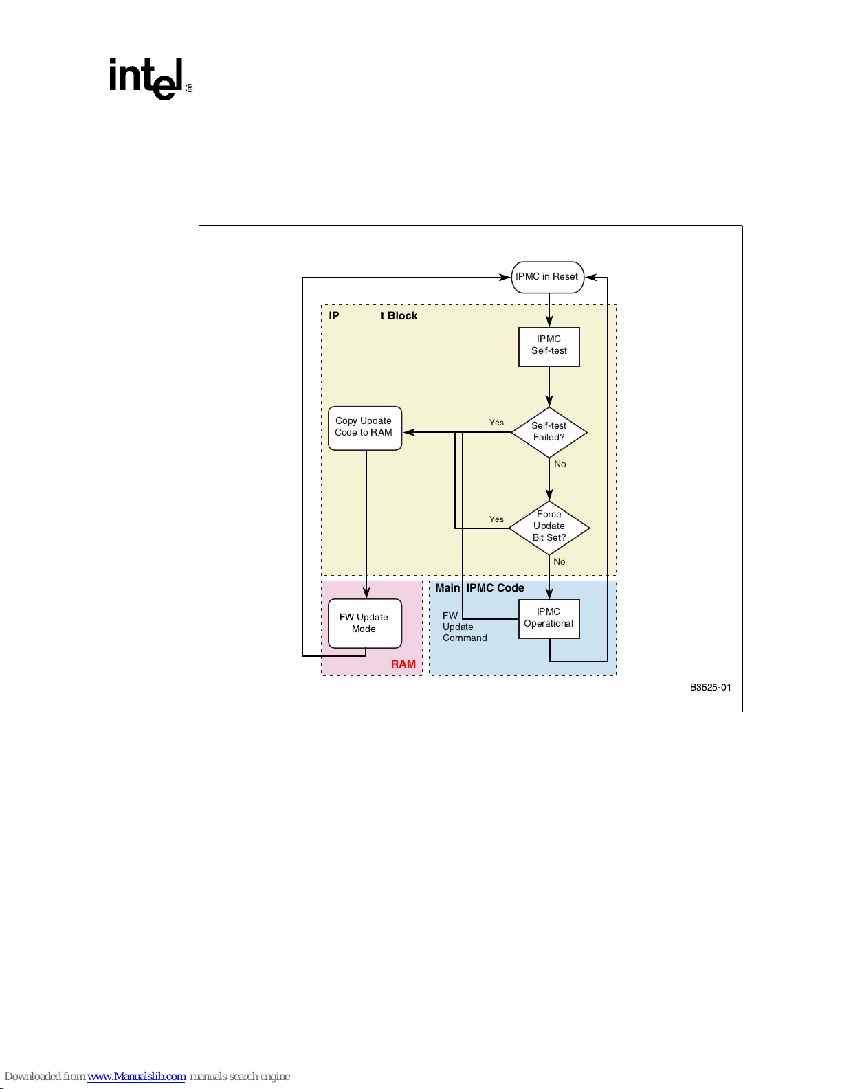
Intel NetStructure® MPCBL0001 High Performance Single Board Computer
When the firmware is commanded to enter firmware (FW) update mode, the oper ational cod e us es
a special branch, Software Interrupt, to jump to the FW update code in the boot block. Once in FW
update mode, the update code is copied into RAM, then the firmware jumps to the code in RAM to
execute. The FW update code cannot execute out of flash while the flash is being updated.
Figure 4. IPMC Firmware Code Process
IPMC Boot Block
Contents
!
!
"#
Main IPMC Code
RAM
"#
"
No
No
!
$"
3.6 IPMC Firmware Upgrade Procedure
MPCBL0001 firmware is upgraded using either of two methods, the KCS interface or the IPMB
(RMCP) interface.
3.6.1 IPMC Firmware Upgrade Using KCS Interface
The KCS interface is the communication mechanism between the host processor on the
MPCBL0001 and the IPMC controller. A firmware update utility is available. It takes a hex file to
be updated as input from the command line. It can also verify that updates are completed
successfully by reading back data written to the flash memory. Typically, it takes the utility around
two minutes to complete the update over the KCS interface. After the firmware update is
Technical Product Specification 47
Order #273817
Page 48

Intel NetStructure® MPCBL0001 High Performance Single Board Computer
Contents
completed, the controller goes through a reset and boots up with the new firmware. The host
processor is not reset when going through a firmware update, so the operating system and
applications running on the host processor are not interrupted.
Please refer to the latest IPMC firmware release notes for the upgrade procedure. The upgrade
procedure, utility, and upgraded firmware are part of the IPMC firmware release package, which
can be downloaded from the Intel web site at http://www.intel.com/design/network/products/cbp/
atca/index.htm.
3.6.2 IPMC Firmware Upgrade via the IPMB Interface (RMCP)
Figure 5. Upgrade via Remote Management Node
Intel® NetStructure™
MPCBL0001 High-
Performance SBC
IPMC
Intel NetStructure
MPCBL0001 High-
Remote
Management
Node
(RMCP Client)
LAN
Shelf
Management
(RMCP Server)
Performance SBC
IPMC
IPMI Specification v1.5 de fines Remo t e Managem e nt Control Protocol (RMCP). Version 1.5 adds
features for layering commands through virtual networks like Ethernet.
The IPMC firmware that needs to be upgraded is loaded to client utility software on the RMCP
client. The RMCP client uses the RMCP protocol carrying embedded IPMI messages to send to the
RMCP Server running in the CMM. The RMCP server decodes the RMCP package and forwards
the IPMI messages to the SBC.
3.6.2.1 Updating MPCBL0001 Firmware
Please refer to the latest IPMC firmware release notes for the upgrade procedure. The upgrade
procedure, utility, and upgraded firmware are part of the IPMC firmware release package, which
can be downloaded from the Intel web site at http://www.intel.com/design/network/products/cbp/
atca/index.htm.
3.7 OEM IPMI Commands
Intel NetStructure
MPCBL0001 High-
Performance SBC
IPMC
B2643-01
This section documents the OEM style IPMI commands implemented and supported on the
MPCBL0001.
48 Technical Product Specification
Order #273817
Page 49

Intel NetStructure® MPCBL0001 High Performance Single Board Computer
3.7.1 Reset BIOS Flash Type
This command resets the processor and changes the BIOS bank select signal so that CPU boots off
redundant BIOS bank.
T able 13. Reset BIOS Flash Type
76543210
NetFn/LUN NetFn = 3Ah (OEM Request) RsLUN
Command Cmd = 01h
Byte 1 BIOS checksum success/failure indication
00h – Checksum success
01h – Checksum failure
Byte 1 Completion code
3.7.2 Set Fibre Channel Port Selection
This command sets the Fibre Channel port routing as specified in the request data bytes. The
command is available over KCS and IPMB interface.
Contents
Table 14. Set Fibre Channel Port Selection
76543210
NetFn/LUN NetFn = 3Ah (OEM Request) RsLUN
Command Cmd = 02h
Byte 1 Intel IANA number (LSB) = 57h
Byte 2 Intel IANA number = 01h
Byte 3 Intel IANA number (MSB) = 00h
Byte 4 Fibre Channel 1 setting, 0=disabled, 1=front panel, 2=Backplane, 3= Reserved, FF=
Byte 5 Fibre Channel 2 setting, 0=disabled, 1=front panel, 2=Backplane, 3= Reserved, FF=
Byte 1 Completion code
Byte 2 Intel IANA number (LSB) = 57h
Byte 3 Intel IANA number = 01h
Byte 4 Intel IANA number (MSB) = 00h
Don’t change settings,
Don’t change settings,
3.7.3 Get Fibre Channel Port Selection
This command returns the current Fibre Channel port ‘routing’ selection. The command is available over the KCS and IPMB interfaces.
Technical Product Specification 49
Order #273817
Page 50

Intel NetStructure® MPCBL0001 High Performance Single Board Computer
Contents
Table 15. Get Fibre Channel Port Selection
76543210
NetFn/LUN NetFn = 3Ah (OEM Request) RsLUN
Command Cmd = 03h
Byte 1 Intel IANA number (LSB) = 57h
Byte 2 Intel IANA number = 01h
Byte 3 Intel IANA number (MSB) = 00h
Byte 1 Completion code
Byte 2 Intel IANA number (LSB) = 57h
Byte 3 Intel IANA number = 01h
Byte 4 Intel IANA number (MSB) = 00h
Byte 5 Fibre Channel 1 setting, 0=disabled, 1= Front panel, 2= Backplane, 3= reserved.
Byte 6 Fibre Channel 2setting, 0=disabled, 1= Front panel, 2= Backplane, 3= reserved.
3.7.4 Get HW Fibre Channel Port Selection
This command returns the current Fibre Channel port routing selection as set in the hardware. The
command is available over KCS and IPMB interface SetFiberChannelPortSelection.
Table 16. Get HW Fibre Channel Port Selection
76543210
NetFn/LUN NetFn = 3Ah (OEM Request) RsLUN
Command Cmd = 04h
Byte 1 Intel IANA number (LSB) = 57h
Byte 2 Intel IANA number = 01h
Byte 3 Intel IANA number (MSB) = 00h
Byte 1 Completion code
Byte 2 Intel IANA number (LSB) = 57h
Byte 3 Intel IANA number = 01h
Byte 4 Intel IANA number (MSB) = 00h
Byte 5 Fibre Channel 1 Settings, 1 = Front Panel, 2 = Backplane
Byte 6 Fibre Channel 2 Settings, 1 = Front Panel, 2 = Backplane
3.7.5 Set Control Sta te
This command sets the state of a control pin and overrides the control pin’s auto state. Refer to
Table 20 on page 52 for control number information.
50 Technical Product Specification
Order #273817
Page 51

Intel NetStructure® MPCBL0001 High Performance Single Board Computer
T able 17. Set Control State
NetFn/LUN NetFn = 3Eh (OEM Request) RsLUN
Command Cmd = 20h
Byte 1 Control number
Byte 2 Control state, 0 = Deassert, 1 = Assert, 3 = Reserved, FF = Don’t change settings
Byte 1 Completion code
Contents
76543210
Technical Product Specification 51
Order #273817
Page 52

Intel NetStructure® MPCBL0001 High Performance Single Board Computer
Contents
3.7.6 Get Control State
This command sets the state of a control pin. This command overrides the AUTO-state of the
control pin. Refer to Table 20 on page 52 for control number information.
Table 18. Get Control State
76543210
NetFn/LUN NetFn = 3Eh (OEM Request) RsLUN
Command Cmd = 21h
Byte 1 Control number
Byte 1 Completion code
Byte 2 Control state, 0 = Deassert, 1 = Assert, 3 = Reserved, FF = Don’t change settings
3.7.7 Get Port80 Data
This command returns the last byte value written by the BIOS to Port 80 since the last System
Reset. If no data has been written to the port since System Reset, the Completion Code returned is
CBh.
T able 19. Get Port80 Data
76543210
NetFn/LUN NetFn = 30h (OEM Request) RsLUN
Command Cmd = 2Dh
Byte 1 — (BLANK)
Byte 1 Completion code
Byte 2 Last Port 80 code value (in HEX)
3.8 Controls Identifier Table
Table 20 below lists the control identifiers that can be used with Set/Get Control State IPMI
commands to query or set information on certain controls in the firmware.
T a ble 20. Controls Identifier Ta ble
Control Description Control Number
FWH Hub (for BIOS bank information) 0 0
FWH 0 Write Protect 1
FWH 1 Write Protect 2
FWH 0 Top Block Lock 3
FWH 1 Top Block Lock4 4
52 Technical Product Specification
Order #273817
Page 53

Intel NetStructure® MPCBL0001 High Performance Single Board Computer
3.9 Hot-Swap Process
The MPCBL0001 SBC has the ability to be hot-swapped in and out of a chassis. The onboard
IPMC manages the SBC’s power-up and power-down transitions. The list below, along with
Figure 6, illustrates this process.
1. Ejector latch is opened. HOT_SWAP_PB# assertion. IPMC firmware detects the assertion of
this signal.
2. IPMC sends "Deactivation Request" message to CMM. M state moves from M4-> M5.
3. Board moves from M5 -> M6 if the CMM grants the request.
4. The IPMC's ACPI timer (3 minutes) starts if an ACPI-enable OS is loaded. Otherwise, it goes
to Step 7 below. The IPMC asserts 20 ms pulse on SMC_PWRBTN#.
5. The Power Button Status register (PWRBTN_STS) is set. It then asserts SCI/SMI# to the OS.
If ACPI OS is enabled, SCI interrupt handler on the OS is called. Interrupt handler clears
PWRBTN_STS bit. OS starts to perform a graceful shutdown.
6. ICH3 detects "LOW" on th e ICH3 _P WR BTN #. Ass ert s ICH3 _S LP_ S 3# an d ICH3_SLP_S5#
to IPMC. Upon detection of ICH3_SLP_S5# and ICH3_SLP_S3#, board transitions to Step 7
below. If ICH3 doesn't assert the signals, the board will transition to Step 7 below upon the
ACPI timer expiration.
7. The firmware deasserts payload power and sets the IPMI locked bit before it transitions from
M6 to M1 state.
Contents
Note: If the upper-level software moves the IPMC to M6, the same procedure is followed, starting with
Step 4.
Figure 6. Hot-Swap Process
ICH3
ACPI-OS
4
5
6
IPMC
1
CMM
2
3
7
Technical Product Specification 53
Order #273817
Page 54

Intel NetStructure® MPCBL0001 High Performance Single Board Computer
Contents
3.9.1 Hot-Swap LED (DS10)
The MPCBL0001 SBC supports one blue Hot Swap LED, mounted on the front panel. See
Figure 14, “MPCBL0001NXX SB C Front Panel” on page 81 for its location. This LED indicates
when it is safe to remove the SBC from the chassis. The on-board IPMC drives this LED to
indicate the hot-swap state. Refer to Table 21, “Hot-Swap LED (DS11)” on page 54.
When the lower ejector handle is disengaged from the faceplate, the hot swap switch embedded in
the PCB will assert a "HOT_SWAP_PB#" signal to the IPMC, and the IPMC will move from the
M4 state to the M5 state. At the M5 state, the IPMC will ask the CMM (or Shelf Manager) for
permission to move to the M6 state. The Hot Swap LED will indicate this state by blinking on for
about 100 milliseconds, followed by 900 milliseconds in the off state. This will occur as long as the
SBC remains in the M5 state. Once permission is received from the CMM or higher- level software,
the SBC will move to the M6 state.
The CMM or higher level software can reject the requ est to move to the M6 state. If this occurs, the
Hot Swap LED returns to a solid off condition, indicating that the SBC has returned to M4 state.
If the SBC reaches the M6 state, either through an extraction request through the lower ejector
handle or a direct command from higher-level software, and an ACPI-enabled OS is loaded on the
SBC, the IPMC communicates to the OS that the module must discontinue operation in p reparation
for removal. The Hot Swap LED continues to flash during this preparation time, just like it does at
the M5 state. When main board power is successfully removed from the SBC, the Hot Swap LED
remains lit, indicating it is safe to remove the SBC from the chassis.
Warning: Removing the SBC prematurely can lead to device corruption or failure.
Table 21. Hot-Swap LED (DS11)
LED Status Meaning
Off Normal status
Blinking Blue Preparing for removal/insertion: Long blink indicates activation is in
Solid Blue Ready for hot swap
progress, short blink when deactivation is in progress.
3.9.2 Ejector Mechanism
In addition to captive retaining screws, the MPCBL0001 SBC has two ejector mechanisms to
provide a positive cam action; This ensures th e blad e is p roperly seated. The bottom ejector handle
also has a switch that is connected to the IPMC to determine if the board has been properly
inserted.
54 Technical Product Specification
Order #273817
Page 55

Intel NetStructure® MPCBL0001 High Performance Single Board Computer
3.10 Interrupts and Error Reporting
3.10.1 Device Interrupts
The Low Voltage Intel® Xeon™ processor and E7501 chipset (MCH, ICH3, P64H2) utilize a
mechanism for delivering interrupts that is slightly different from, though fully compatible with,
previous IA-32 syst em pl atforms. The change aff ects only the delivery mechanism and no changes
are required to existing software.
This new delivery mechanism transfers the equivalent APIC messages across the system bus
structure rather than using a sideband channel as in the case of the APIC serial bus. There is no
longer an APIC bus connection to the processor. This new mechanism improves the interrupt
message transfer speed to the processors, thus reducing latency. It also simplifies the flushing of
buffers that is required when data is buffered between the I/O subsystem and memory. Since
interrupt messages are no longer communicated acro ss a si deban d channel, these transfers are now
visible to the chipset. The interrupt message transactions themselves can now initiate buffer
flushing to ensure all data within the I/O and memory subsystems is coherent.
As before, the LINT[1:0] connections to the processors remain for compatibility with the old PC
industry standard, legacy interrupt architecture (8259 controllers). In addition, the P64H2 PCI
bridge devices include an interrupt output (BTINTR#), which can be routed into the legacy
interrupt controller to facilitate booting from devices residing on the far side of such PCI bridge
devices. Once the boot process is complete and the APIC interrupt system is enabled, devices no
longer need to share interrupts; This improves interrupt system performance.
Contents
The BIOS initializes and enables both the 8259 and APIC but masks all APIC interrupts in the
redirection table. This is so the SBC operates in legacy interrupt mode. Th e BI OS does no t op erate
in APIC mode at any time. An APIC-aware OS disables the 82 59 and unmasks the APIC interr upts
to switch to APIC mode.
Table 22 displays the interrupt connections provided by the MPCBL0001 SBC. Actual interrupt
vector assignments and routing to legacy interrupts as necessary is under BIOS and/or OS control.
Table 22. Interrupt Assignments (Sheet 1 of 2)
Legacy Interrupt IRQ assigned
Master 8259
Internal timer0 output 0
Slave 8259 INTR output 2
Serial Port A 3
Slave 8259
Internal RTC 0 (8)
Primary IDE 6 (14)
PCI Device Interrupt IRQ assigned
HI-A ICH3
Super I/O SERIRQ
USB 1.1 controller #1 PIRQA#
IPMC_SYSIRQ# PIRQB#
Technical Product Specification 55
Order #273817
Page 56

Intel NetStructure® MPCBL0001 High Performance Single Board Computer
Contents
Table 22. Interrupt Assignments (Sheet 2 of 2)
Legacy Interrupt IRQ assigned
HI-B P64H2 BTINTR# PIRQC#
HI-C P64H2 BTINTR# PIRQD#
HI-B P64H2
Fibre Channel INTA# PB_IRQ0
Fibre Channel INTB# PB_IRQ1
HI-C P64H2
PMC INTA# PA_IRQ0
PMC INTB# PA_IRQ1
PMC INTC# PA_IRQ2
PMC INTD# PA_IRQ3
Ethernet #1 INTA# PB_IRQ0
Ethernet #2 INTA# PB_IRQ1
Figure 7. Interrupt Signals
Low Voltage
®
Intel
Xeon
Processor
MCH
8-Bit
HL_A
ICH3
10x
APIC
LPC
Super I/O
LINT0 / INTR
LINT0 / NMI
Low Voltage
®
Intel
Xeon
®
Processor
®
FSB
Redirection Logic
16-Bit
HL_B
P64H2
10x
APIC
PCI-X
Fibre
Channel
P64H2
10x
APIC
GbE
(x2)
16-Bit
HL_C
PCI-X
PMC
Slot
PCI
64/66
56 Technical Product Specification
B0754-01
Order #273817
Page 57

Intel NetStructure® MPCBL0001 High Performance Single Board Computer
3.10.2 Error Reporting
The MCH handles error reporting from the memory subsystem. Errors consist of correctable and
uncorrectable bit errors. The ECC algorithms used are capable of correcting any number of bit
errors contained within a 4-b i t nibbl e. In addition, any number of b i t error s contai ned w ith in t wo 4 bit nibbles is detected. The MCH communicates these errors to the ICH3 via special cycles over the
hub link interface. These special cycles indicate to the ICH3 that an MCH-detected error has
occurred. The MCH special cycle communicates the type of event that should be genera ted by the
ICH3 when an error is detected. Selection for the generation of an SERR, SMI, or SCI event is
provided. Status for these reported errors is then found in the MCH DRAM_FERR (first error) and
DRAM_NERR (next error) status registers. Refer to the MCH data s heet for more information (see
Appendix A, “Reference Documents”).
Correctable memory errors generate an SMI and are logged via IPMI as a SEL. Non-correctable
errors first generate an SMI (which generates a SEL) and then an NMI.
Each P64H2 device reports the PCI errors that occur on the buses to which it is attached. These
consist of the PCI error assertions of the PERR# or SERR# signals. The errors are reported by
sending the DO_SERR special cycle to the MCH on the Hub Interface. The MCH forwards the
error to the ICH3, which generates the appropriate erro r condition to the pro cessor(s) su ch as NMI,
SMI, or SCI.
Contents
PCI address parity errors are considered catastrophic and may abort further data tra nsfers by the
P64H2 if that is the programmed response. Parity/ECC is checked on both the Hub Interface and
PCI bus transactions. PCI data parity errors are considered less severe and allow transactions to
continue. Data parity errors cause the Detected Parity Error” status to be logged and, if enabled, the
DO_SERR special cycle is transmitted. In a transaction where a data error occurs, the data being
forwarded to the next bus is “poisoned” to ensure the error follows the data to its destination.
Poisoned data has bad parity or multi-bit ECC errors introduced before being forwarded to the next
bus.
PCI assertions of the SERR# signal also result in the DO_SERR special cycle being generated on
the hub interface when enabled. Other potential causes for a DO_SERR special cycle include:
• Parity errors on the target bus during a write.
• A master timeout on a delayed transaction.
• The occurrence of a PCI master abort cycle.
Refer to the P64H2 Data Sheet, section 4.9, for more information on error handling. For details on
obtaining this document, see Appendix A, “Reference Documents.”
The ICH3 device has the ability to report PCI and hub link errors directly to the processors. When
a PERR# or SERR# occurs on the ICH3 local PCI bus, the ICH3 can be programmed to generate
NMI or SMI. The ICH3 also fields messages from the MCH and its attached hub devices to
indicate errors to the processors on their behalf. The messages may request SMI#, SCI, NMI, or
SERR3 to be asserted. Software must check the MCH and attached hub devices to determine the
exact cause of the error. Refer to the ICH3 Data Sheet for more information on error handling and
generation. For details on obtaining this document, see Appendix A, “Reference Documents.”
Technical Product Specification 57
Order #273817
Page 58

Intel NetStructure® MPCBL0001 High Performance Single Board Computer
Contents
3.11 ACPI
ACPI gives the operating system direct control over the power management and Plug and Play
functions of a computer. The use of ACPI with theMPCBL0001 SBC requires an operating system
that provides ACPI support. ACPI features include:
• Plug and Play (including bus and device enumeration) and APM support (normally contained
in the BIOS).
• Power management control of individual devices, add-in boards (some PMC cards may
require an ACPI-aware driver), and hard-disk drives.
• A soft-off feature that enables the operating system to power off the computer.
• Support for an IPMC firmware command switch.
3.11.1 System States and Power States
Under ACPI, the operating system directs all system and device power state transitions. The
operating system puts devices in and out of low-power states based on user preferences and
knowledge of how devices are being used by applications. Devices that are not being used can be
turned off. The operating system uses information from applications and user settings to put the
system as a whole into a low-power state.
Table 23, “Power States and Targeted System Power” on page 58 lists the power states and the
associated system power targets supported by the MPCBL0001 SBC. See the ACPI Specification
for a complete description of the various system and power states.
3.12 Reset Types
Ta ble 23. Power States and Targeted System Power
Global States Sleeping States
G0 – working state S0 – working C0 – working D0 – working state.
G1 – sleeping state S4 – Suspend to disk.
G2/S5 S5 – Soft off. Context
G3 – mechanical off
AC power is disconnected
from the computer.
The watchdog timer on the IPMC can be configured and used through standard IPMI v1.5
watchdog timer commands. Refer to Section 3.13.1, “WDT #1” on page 64 for detailed
implementation.
Context saved to disk.
not saved. Cold boot is
required.
No power to the system. No power D3 – no power for wake up
Processor
States
No power D3 – no power except for wake
No power D3 – no power except for wake
Device States
up logic.
up logic.
logic, except when provided by
battery or external source.
58 Technical Product Specification
Order #273817
Page 59

Intel NetStructure® MPCBL0001 High Performance Single Board Computer
3.12.1 Reset Logic
The following topics describe the two types of reset requests and the boot relationships among
them. The two types of reset requests available on the MPCBL0001 are:
• Hard reset request (always results in a cold boot)
• Soft reset request (can result in either a warm or cold boot)
A hard reset request occurs whenever the processor Reset line is asserted and then deasserted. A
soft reset occurs whenever an assertion occurs on the processor Init line. Whenever a soft reset
request occurs, the BIOS checks two memory locations to determine whether to initiate a warm
boot while leaving main memory intact or a cold boot that clears memory.
Whenever the BIOS detects that the reset is either a hard reset or a cold boot, it specifically clears
the memory location 40h:72h so it does not contain a 1234h. Under warm boot conditions, this
memory location contains a 1234h (the developer’s application writes this value in this location
[using /dev/mem] when it is started). If a hard reset occurs (as defined in the hard reset topic
below), it is certain that the 40h:72h location contains a non-1234h value.
3.12.2 Hard Reset Request
Contents
A Hard Reset, or CPU Reset, is defined as the assertion of the processor reset signal (see Table 24,
“Reset Request” on page 60). This initializes the processor state and registers, disables internal
caches, and causes the processor to unconditionally begin execution from the reset vector. A hard
reset is initiated by the following events:
1. A power up of the SBC. The SMC enables the onboard power supplies.
2. The SMC negates the ICH3_PWROK signal (see Note below).
3. A “reset” command from the Port CF9h I/O register (refer to the “Intel
Controller Hub 3 (ICH3-S) Datasheet” for information about this register).
4. Watchdog timer (WDT #1) expires and is configured to initiate a hard reset. See “Watchdog
Timers (WDTs)” on page 64 for more information.
5. Watch dog timer (WDT #3) expires after failure to perform the first instruction fetch.
6. A command (cmmset -l bladex -d powerstate -v reset) is issued from MPCMM0001.
Note: The IPMC can negate the dedicated signal ICH3_PWROK to initiate a processor reset.
ICH3_PWROK indicates whether power is OK. If the IPMC deasserts ICH3_PWROK, the
hardware asserts the processor reset lines.
3.12.3 Soft Reset Request
The assertion of the processor’s INIT signal causes a soft reset or “CPU INIT” (see Table 24,
“Reset Request” on page 60). The ICH3 is normally responsib le for driving the INIT signal. A
CPU INIT event causes the processor(s) to fetch the reset vector at the next instruction boundary.
The majority of the processor and all of the cache states are unaffected by an INIT event.
®
82801CA I/O
After the INIT event, hardware may be reset (or not r eset) u nd er BI OS control. PCI buses are reset
using their respective bridge control registers. This signal is then level translated to the processor
compatible signal level. INIT may be caused by the following events:
Technical Product Specification 59
Order #273817
Page 60

Intel NetStructure® MPCBL0001 High Performance Single Board Computer
Contents
1. The reset button is pressed (see Note below). See Figure 14, “MPCBL0001NXX SBC Front
Panel” on page 81 for its location.
2. A processor shutdown special cycle occurred.
3. An INIT command from Port 92h I/O reg ister (refer to the Intel
®
82801CA I/O Contr o ller Hub
3 (ICH3-S) Datasheet for information about this register).
4. An INIT command from Port CF9h I/O register.
5. A keyboard reset command (ICH3 RCIN# signal asserted).
6. The IPMC may also directly assert the INIT signal; WDT #1 expires and is configured for a
soft reset.
7. Processor BIST is enabled and a hard reset is initiated from the Port CF9h register. This asserts
the INIT signal but is not classified as a soft reset since CPU reset is also asserted.
8. OS reboot commands (eg: "shutdown -r now" or "reboot" in Linux).
9. A processor INIT may also be initiated through an APIC “init” message. This message may
target a specific processor or all processors. This “init” is an internally generated event (No
INIT signal is asserted) so the IPMC is unable to detect this occurrence.
Note: The reset button (RESET_PB#) is an input to the IPMC. There are also IPMI commands to reset
the board and change power states through the software. However, the reset button is a last resort
because the user must be physically present at the chassis to reset the board.
After a Soft Reset/CPU Init, the BIOS code executes and determines if the reset is a warm boot or
a cold boot. A warm boot restarts the system and keeps memory above the 8 MByte boundary
intact. During a warm boot the MCH is not reset, allowing DRAM refresh to continue during and
over the soft reset event. A cold boot sets the state of all peripherals to the same state they would be
in if a hard reset were triggered.
T able 24. Reset Request
Reset Request Signal Activated Type
Hard Reset Full reboot
Soft Init Partial reboot
3.12.4 Warm Boot
A warm boot occurs when the processor is booting after a soft reset request. To qualify as a warm
boot, the reset counter l ocated at 40h : D0h m ust be n on- zero (by default, the reset co unter and reset
flag are initialized to 10 and 1234h by BIOS after a cold boot.) Execution starts at the reset vector.
The BIOS initializes and configures all devices except for memory . Memory contents remain intact
except for the first 8 MBytes. Th e BIOS u ses th e firs t 8 MBytes duri ng POST, but does not modify
the reset flag or the reset counter . MCH is not reset, allowing DRAM refresh to continue during the
warm boot.
Note: On every warm boot, BIOS automatically decrements the reset counter by one. When the reset
counter reaches zero and the soft reset is initiated, a cold boot occurs instead of warm boot.
60 Technical Product Specification
Order #273817
Page 61

Intel NetStructure® MPCBL0001 High Performance Single Board Computer
3.12.5 Co ld Boot
Any soft reset that does not meet the configurat ion descri bed in th e preceding Warm Boot section is
classified as a cold boot. Execution starts at the reset vector, and BIOS initializes and configures all
devices, including memory subsystem, as if a hard reset had occurred. See Table 25, “Reset
Actions” on page 61.
During a cold boot the BIOS initializes the warm reset counter to 0x0A and clears the reset flag to
1234h. Software can then read the reset flag to determine the type of reset.
Table 25. Reset Actions
Reset Actions System Function Memory Status
Warm boot Partial restart Preserves memory above 8MB boundary
Cold boot Full restart Functionally equivalent to a hard reset.
3.12.6 Power Good
When the MPCBL0001 SBC is inserted into the chassis, the hardware management circuitry is
“hot plugged.” The hardware management voltage is immediately applied, and the on-board IPMC
is reset. After the hardware management reset, the operation of the IPMC and full power-up of the
SBC are under firmware control.
Contents
Upon command to power on the module, the IPMC asserts the “power enable” signal to the onboard DC/DC converters. Full power-up of the SBC is sequenced by hardware to ensure devicespecific power requirements are followed. Sequencing of specific voltages is required to ensure
that devices using multiple voltages are not damaged or stressed.
Figure 8. Power Good Map
VRM
Controller
Intelligent Platform
Management
Controller
(IPMC)
Power
Goods
PLD
VRM_PWRGOOD
ICH3_PWROK
ICH3
E7501
MCH
82546
Dual
GbEnet
H_PWRGD
ICH3_PCIRST#
Low Voltage
®
Xeon™
Intel
Processor
Low Voltage
®
Xeon™
Intel
Processor
ICH3_PCIRST#
(global reset)
Technical Product Specification 61
Order #273817
B0895-02
Page 62

Intel NetStructure® MPCBL0001 High Performance Single Board Computer
Contents
As the many voltages power up, each regulator produces a “power go od” signal. All of these power
good signals are logically OR’d (with the exception of the VRM power good) to produce the
ICH3_PWROK signal in put to the I CH3 as s how n in Figure 8, Power Good Map. When this sign al
is active, it indicates all on-board power is good.
Next, the VRM power good is gated with the ICH3_PWROK signal in the ICH3 to produce the
processor’s power good signal input.
As soon as the ICH3 device is powered, its PCI reset output is asserted. This reset output remains
asserted until all power good signals are present (indicated by the ICH3_PWROK signal), the
processor VRM power good signal is asserted, and device voltage/clock stabilization times have
been satisfied.
Device resets are then released, and processor BIOS execution and boot begins. The PCI reset
output of the ICH3 is the source of all other power-up reset signals as shown in Figure 9, “Reset
Chain” on page 63
The IPMC is also capable of initiating this power-up or global reset by negating the
ICH3_PWROK signal. Additio nall y, devices on specific PCI buses may be independently reset by
software through their associated bridge devices.
When commanded to do so, the IPMC releases device and processor resets, and processor BIOS
execution and boot be gins.
62 Technical Product Specification
Order #273817
Page 63
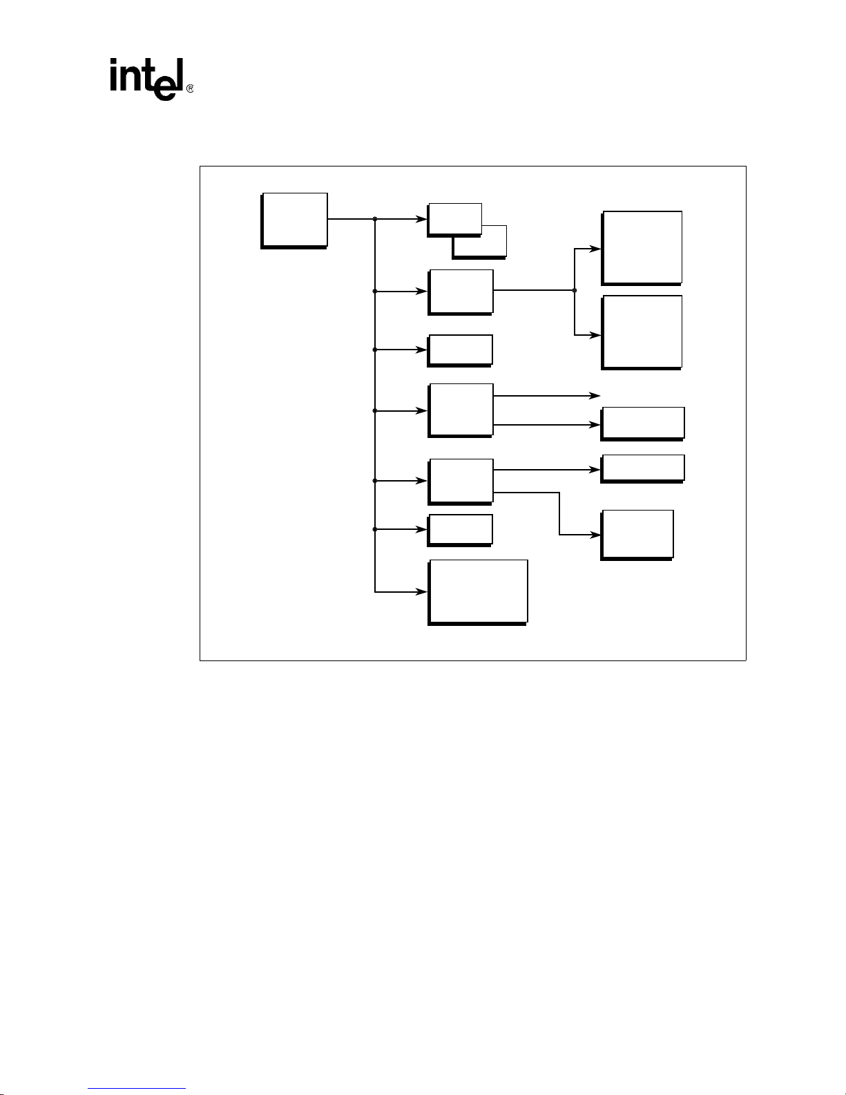
Intel NetStructure® MPCBL0001 High Performance Single Board Computer
Figure 9. Reset Chain
Contents
ICH3
ICH3_PCIRST#
FWH 0
FWH 1
E7501
MCH
DIMMs
PCIRST A
HI-B
P64H2
PCIRST B
PCIRST A
HI-C
P64H2
PCIRST B
Super I/O
IPMC
(Intelligent Platform
Management
Controller)
H_CPURST
Low Voltage
®
Xeon™
Intel
Processor
Low Voltage
®
Xeon™
Intel
Processor
<unused>
Fiber Channel
Controller
PMC card
82546
Dual
GbEnet
B0896-02
Technical Product Specification 63
Order #273817
Page 64

Intel NetStructure® MPCBL0001 High Performance Single Board Computer
Contents
3.13 Watchdog Timers (WDTs)
Figure 10, “Watchdog Timers” on page 64 shows the relationship between the three watchdog
timers (WDTs) on the MPCBL0001 SBC.
Figure 10. Watchdog Timers
ICH3
(South Bridge)
WDT #3
3.13.1 WDT #1
The first WDT (WDT #1) is a hardware timer in the IPMC. WDT #1 is IPMI compliant; its
interaction with the host processor BIOS or system software is accomplished through IPMI
commands over the Keyboard Controller Style (KCS) interface to the IPMC. The host processor
uses the Set Watchdog Timer message to configure WDT #1, then the Reset Watchdog Timer
message to strobe the timer.
Strobe
IPMB-A
Isolation Logic
Host
Processor(s)
IPMC
WDT #1
Strobe
Strobe
PLD
WDT #2
IPMB-B
Isolation Logic
B1368-02
WDT #1 can be set to any value between 100 ms and 6,553,600 ms in 100 ms intervals. Another
configuration parameter is an indicator of which software is controlling WDT #1. This has five
state settings:
1. BIOS FRB2: Used during fault-resilient booting to detect iss ues in the BIOS.
2. BIOS/POST: Used while the BIOS is running through its POST operations.
3. OS Load: Set by the BIOS just before an OS load, then reset by the OS (the OS must be
enabled to do so) when it finishes booting.
4. SMS/OS: Used by the system management software or the OS.
5. OEM: Used by any OEM software.
64 Technical Product Specification
Order #273817
Page 65

Intel NetStructure® MPCBL0001 High Performance Single Board Computer
Contents
WDT #1 can also be configured to take variou s actions befo re timin g out (for examp le, SMI, NMI,
nothing) or after timing out (for example, hard reset, power down, or power cycle). In addition, an
event can be logged into the SEL whenever the watchdog timer expires. If WDT #1 expires, the
IPMC is not reset. For more details on the watchdog timer commands and settings, see the IPMI
Specification version 1.5.
On power up, the initial state is that the IPMI WDT #1 is not running. Normally some code (BIOS
or OS level) must send the Reset Watchdog Timer command to start the timer running. The same
code sends a Set Watchdog Timer command first to set up the timer to a k nown state (s ee the IPMI
Specification for more details).
When WDT #1 times out, it logs an event into the SEL, provided that the “Don’t Log” flag is false
(see the IPMI 1.5 Specification for details). The SEL event also describes the timeout action taken.
If WDT #1 times out and causes a hard reset, the timer state is equivalent to the power-up state
(that is, not running; either BIOS or the OS must configure and start it). If the host processor is
reset (soft or hard) independent of WDT #1, the firmware disables the watchdog timer.
One of the actions BIOS takes very early in its code is to start the WDT #1 to monitor its boot
progress. When it finishes POST, the BIOS turns off WDT #1 during the OS load period.
WDT #1 parameters are altered according to BIOS control parameters , and WDT #1 is no t running
when the OS first (re)starts. The BIOS sets WDT #1 to a length of time longer than the expected
POST time; therefore, BIOS does not actively strobe WDT #1. The flag that determines if a WDT
#1 reset must be hard or soft remains over any type of reset, since it is held in the microcontroller.
3.13.2 WDT #2
WDT #2 (implemented in a PLD) must be strobed by the IPMC firmware. If WDT #2 expires, it
isolates the SBC from the backplane IPMB buses and resets the IPMC. There is no method for the
processor to be explicitly notified that the IPMC is reset. Once the IPMC has reset, the main
processors can resume communication with the IPMC. The watchdog timer is set to trigger after 96
seconds, and the IPMC strobes it once a second.
WDT #2 is always running; that is, the counter is always counting. However, a PLD component
controls the IPMC reset and IPMB isolation associated with WDT #2 expiration, ignoring any
WDT event until the IPMC strobes/enables the LTC4300 IPMB interfaces.
3.13.3 WDT #3
WDT #3 is contained within the ICH3 device. This watchdog timer monitors the processor’s first
attempt to fetch an instruction after a power up or hard reset. If the processor has not fetched its
first instruction within the timeout period, the ICH3 resets the processors. Since the processor has
not begun any execution, the ICH3 uses a hard reset.
Technical Product Specification 65
Order #273817
Page 66

Intel NetStructure® MPCBL0001 High Performance Single Board Computer
Contents
3.14 LED Status
3.14.1 Health LED
The MPCBL0001 SBC supports one bicolor health LED to indicate the SBC’s health status, i.e.,
whether a fault or error condition has been detected on the SBC. This LED is mounted on the front
faceplate and driven by the onboard IPMC. The health LED will only be driven to an error
condition (red) if there is a critical or non-recoverable (major or critical in AdvancedTCA
parlance) condition active on the SBC. Alarms could include exceeding sensor thresholds for
temperature and on-board logic voltages. The health LED remains red until the sensors return to a
normal operating value. Hard-drive failures, boot failures, etc. are not considered critical/major
IPMI states, so the IPMC does not explicitly set the health LED in these cases.
Note: The LED's error state color defaults to red, but the color can be overridden. using PICMG 3.0-
defined commands. Refer to Section 3.14.9, “Setting the Default Color for the OOS and Health
T a ble 26. Health LED
LEDs” on page 69.
LED Status (right) Meaning
Solid Green Healthy
Solid Amber/Red Fault or error condition
The default color and override capabilities of the LED follow the LED management requirements
defined in Section 3.14.9, “Setting the Default Color for the OOS and Health LEDs” on page 69.
3.14.2 OOS (Out Of Service) LED
The MPCBL0001 SBC supports one bicolor “OOS” LED, mounted on the front faceplate. The
LED can be driven to display a red or amber color. When this LED is lit, it indicates that the board
is not in service. Its back-end (payload) power could be OFF or ON. Often the OOS state is entered
when a critical fault occurs on the board. In this state, the back-end (payload) power is turned OFF.
A board could be in this state when its back-end power is OFF but healthy, or when a board is fully
powered but not yet deployed, or during the reset process.
Note: Do not extract a board unless the Hot Swap LED is lit.
Table 27. OOS LED (DS9)
LED Status (left) Meaning
Off In service
Solid Amber/Red Fault or error condition
The default color and override capabilities of the LED follow the LED management requirements
defined in Section 3.14.9, “Setting the Default Color for the OOS and Health LEDs” on page 69.
3.14.3 Hot-Swap LED
See Section 3.9, “Hot-Swap Process” on page 53.
66 Technical Product Specification
Order #273817
Page 67

Intel NetStructure® MPCBL0001 High Performance Single Board Computer
3.14.4 IDE Drive Activity LED
Table 28. IDE Drive Activity LED
LED Status Meaning
Off Normal/No disk access
Green (Blinking) Disk access (read/write activity)
3.14.5 User Programmable LEDs
The MPCBL0001 SBC provides two bicolor LEDs for user-programmable functions. The LEDs
can be driven to display a red, gr een or amb er colo r. When these LEDs are lit, they indicate a status
of a user-defined function.
Table 29. User Programmable LEDs
LED Status (left) LED Status (right) Meaning
Off Off No Status
Red Red/Green Active Status of user defined function
Contents
The user-programmable LEDs are connected to the GPIO pins on the ICH3 device as follows:
Table 30. GPIO Pin Connections
PIN GPIO Pin Default Value LED Color
User_Prog_LED1_Red# GPIO21 1 Off
User_Prog_LED1_GRN# GPIO20 1 Off
User_Prog_LED2_Red# GPIO28 1 Off
User_Prog_LED2_GRN# GPIO23 0 Green
By programming the ICH3 GPIO registers as outputs, then selecting the appropriate state (low for
illumination, high for off), the user enables the LEDs as required. Refer to the ICH3 datasheet in
appendix B for specific GPIO 20, 21, 23, 28 register information.
Technical Product Specification 67
Order #273817
Page 68

Intel NetStructure® MPCBL0001 High Performance Single Board Computer
Contents
3.14.6 Network Link/Speed LEDs
The front panel of the SBC provides two LEDs for each Ethernet connection indicating the speed
and link activity for that network connection:
Table 31. Network Link LEDs
For Channel A : L2 / For Channel B : L6
Link LED Sta tus Meaning
Off No link
Solid Green Link established
Blinking Green Link with activity
NOTE: Refer to Figure 14 and Figure 15 for LED (L2 and L6) placement on the
Table 32. Network Speed LEDs
Front Panel.
For Ethernet controller Channel A : L3 & L4
Speed LED Status
L3 L4
Solid Yellow Off 1 Gbps connection
Off Solid Green 100 Mbps connection
Off Off 10 Mbps connection
For Ethernet controller Channel B : L7 & L8
Speed LED Status
L7 L8
Solid Yellow Off 1 Gbps connection
Off Solid Green 100 Mbps connection
Off Off 10 Mbps connection
NOTE: Refer to Figure 14 and Figure 15 for LED (L3, L4, L7 and L8) placement
on the Front Panel.
Meaning
Meaning
3.14.7 Ethernet Controller Port State LEDs
The front panel of the SBC provides a bicolor LED for each Ethernet channel that can light to
indicate the Ethernet port state. These LEDs can display a red, green or amber color. The function
of the port state LEDs is user definable. The Ethernet Controller SDP[6:7] GPIO bits for each
channel are the outputs that control the LEDs. SDP[6] is connected to the Green LED, and SPD[7]
is connected to the Red LED.
Refer to the documentation for the Intel
on how to drive these LED signals. Note that existing network drivers may drive these GPIO pins.
68 Technical Product Specification
®
82546 Dual Gigabit Ethernet Controller for information
Order #273817
Page 69

Intel NetStructure® MPCBL0001 High Performance Single Board Computer
Table 33. Ethernet Controller Port State LED
LED Status (L1 and L5) Meaning
Off No Status
Red/Green/Amber Active status of user-defined function
NOTE: Refer to Figure 14 and Figure 15 for LED (L1 and L5) placement on the
Front Panel.
3.14.8 Fibre Channel Port State LEDs
The MPCBL0001 SBC supports two Fibre Channel port state LEDs mounted on the front
faceplate. The LEDs are green and yellow. When this LED is lit, it indicates the port state of each
Fibre Channel port. LED states are shown in the table as follows:
Table 34. Fibre Channel Port State LED (DS2, DS3)
Contents
Yellow LED Status ( Fibre
Channel 1, left)
ON ON Power On
Flashing OFF Loss-of-Sync
ON OFF Signal Acquired
OFF ON On-Line
FLASH FLASH F/W Error
Green LED Status (Fibre
Channel 2, right)
Meaning
3.14.9 Setting the Default Color for the OOS and Health LEDs
The current default color Health LED in any assertion event is RED. As for the OOS LED, the
default color is also RED if there is a fault or error condition.
With the latest IPMC Firmware 1.17, the user has the ability to set the default color to AMBER due
to geographical requirements. This default LED color will stay persistent upon IPMC reset.
The PICMG SetFRULedState command used with Function code 0xFC will now persistently save
the supplied explicit color and make it the new Local Control “Asserted” state color. This only
works with valid colors (not 0x0e or 0x0f).
So, for example, to set the default “Asserted” color of the Health LED from RED to AMBER, the
following IPMI command should be issued:
NetFn: 0x2C PICMG 3.0 Extension
Cmd: 0x07 SetFRULedState command
Data 1: 0x00 PICMG Identifier
Data 2: 0x00 FRU Device ID
Data 3: 0x02 LED ID (LED 2 = Health LED)
Data 4: 0xFC LED Function (Restore Local Control)
Data 5: 0x00 On-Duration (ignored)
Data 6: 0x04 LED Color (4 = Amber)
After this command is executed, the Health LED will illuminate as AMBER instead of RED on an
unhealthy event. The “Unasserted” color will remain GREEN.
Technical Product Specification 69
Order #273817
Page 70

Intel NetStructure® MPCBL0001 High Performance Single Board Computer
Contents
Caution: Do not change the Health LED default color to GREEN. Doing so will cause no color change on
unhealthy events!
3.15 FRU Payload Control
The MPCBL0001 implements the “FRU Control” command as specified in the PICMG 3.0
Specification. Through this command, the payload can be reset, rebooted, or have its diagnostics
initiated.
The FRU payload can be controlled by a command line via the Intel NetStructure
Chassis Management Module (CMM). The following CMM commands are supported by the
MPCBL0001.
Table 35. CMM Commands for FRU Control Options
FRU Control Options MPCMM0001 equivalent command
Cold Reset cmmset –l bladex –d frucontrol –v 0
Warm Reset cmmset –l bladex –d frucontrol –v 1
Graceful Reboot cmmset –l bladex –d frucontrol –v 2
Diagnostic Interrupt cmmset –l bladex –d frucontrol –v 3
Note: The user may issue an RMCP command to control the FR U pay l oad as well. Refer to Table 108 on
page 189 for the associated IPMI command information.
3.15.1 Cold Reset
When this command is initiated, the board will perform a hard reset as described in Section 3.12.2,
“Hard Reset Request” on page 59.
3.15.2 Warm Reset
When this command is initiated, the board will perform a soft reset as described in Section 3.12.3,
“Soft Reset Request” on page 59.
®
MPCMM0001
3.15.3 Graceful Reboot
This specific payload control command is implemented using system interface messaging
capability and the SMS_ATN bit of the KCS status registers.
The Receive Message Queue is used to hold message data for system software until the system
software can collect it, while the SMS_ATN bit is used to indicate that the IPMC requires attention
from the system software.
The flow diagram below will assist the user who will be developing their system software to
interact with this command.
70 Technical Product Specification
Order #273817
Page 71

Intel NetStructure® MPCBL0001 High Performance Single Board Computer
Figure 11. Flow Diagram for Graceful Reboot Command
Contents
OS Agent
3
Asserts SMS_ATN signal
Get Message
4
IPMC CMM
IPMB In t e r face KCS Interface
Cmmset –l bladex –d frucontrol –v 2
1
1. MM sends a frucontrol=2 command to IPMC, initiating a graceful reboot.
2. When the IPMC receives frucontrol=2, it formats a message into the send message queue and
sets the SMS attention flag (SMS_ATN) on the KCS status register.
3. OS Agent polls for SMS_ATN using Get Message Flags command.
4. OS Agent sends a Get Message command to the IPMC to retrieve the message from the
receive message queue. The Get Message command returns the following data:
Table 36. Returned Values from the Get Message Command
Byte Data Value Comments
1 Completion Code 00h
2 Channel 40h Administrator privilege, Channel 0 (IPMB 0)
3 NetFN/rsLUN C2h NetFn=30h, Responder LUN=02h (SMS)
4 Header checksum 3Eh 2’s complement of the previous byte (chk1)
5 BMC Address (varies) Board’s IPMB address (depends on slot)
6 Sequence/rqLUN 04h Sequence=01h, Requestor LUN=00h (IPMB)
7 Command 10h Intel’s command for shutdown/reboot
8 Data 02h Reboot action
9 Data checksum 5F 2’s complement of the sum of the previous 4 bytes (chk2)
3.15.4 Diagnostic Interrupt
The following command provides the capability for an end user to issue a non-maskable interrupt
(NMI) to the payload.
When issued, the NMI signal to the processor will be asserted. To fully utilize the support of this
command, the user needs to have an NMI handler installed.
Technical Product Specification 71
Order #273817
Page 72

Intel NetStructure® MPCBL0001 High Performance Single Board Computer
Contents
The implementation details are as below:
Figure 12. Diagnostic Interrupt Command Implementation
CPU
(H_NMI)
2
Asserts NMI signal
IPMC CMM
Cmmset –l bladex –d frucontrol –v 3
1. CMM sends a frucontrol=3 command to IPMC initiating a diagnostic interrupt.
2. When the IPMC receives frucontrol=3, it asserts the NMI signal to the CPU via the GPIO pins
connected to the H_NMI pin.
3.16 Serial Port Buffering Overview
Serial port buffering occurs when the IPMC o n the blade reads and bu f fers characters coming from
a serial console port on the Super I/O chipset used in the SBC. This serial data could be from the
operating system, such as Linux, runn i ng on th e blade. This data could then be read back via IPMI
commands via the shelf manager so that an operator can see a “snapshot” of the last few lines of
text output by the blade before it crashed or otherwise stopped working.
IPMB Interface GPIO
1
The buffer in the IPMC used to store the serial information is 2048 (0800h) bytes. It is big enough
to hold an 80x25 screen of data with a CR/LF pair at the end of 24 lines. When the buffer fills, it
wraps around so that the oldest data is overwritten by newer data.
The board uses a Super I/O controller that has two RS232 serial ports. The first port (COM1) is
routed to the front panel of the blade and has no connectivity to the IPMC. The second serial port
(COM2) is only connected directly to a serial port on the IPMC. Any data that n eeds to be buf fered,
therefore, needs to be directed out the second serial por t (COM2 ). Data comi ng from COM1 cannot
be monitored or buffered by the IPMC.
This feature also provides the capability to filter out certain ANSI escape sequences coming into
the serial port. This is so the buffer does not fill with escape sequences that provide no meaningful
content. This is parti cularly true o f messages output by BIOS duri ng startup. If only Linux outp ut is
desired, then the filtering option is probably not needed.
When enabled, the filter prevents the buffering of the following escape sequences:
72 Technical Product Specification
Order #273817
Page 73

Intel NetStructure® MPCBL0001 High Performance Single Board Computer
T a ble 37. Escape Sequences Not Buffered with Filter Enabled
Description PC ANSI Codes
Move cursor up 1 row ESC [ A
Move cursor down 1 row ESC [ B
Move cursor right 1 column ESC [ C
Move cursor left 1 column ESC [ D
Home ESC [ H
End ESC [ K
Clear Display Screen ESC [ 2 J
Set cursor position to row;col. ESC [ row;col H
Set Text Attributes ESC [x;y;z m
3.16.1 Using Serial Port Buffering
3.16.1.1 Configuring the Serial Port
Contents
In order for the IPMC to correctly buffer characters it receives from its serial port, the serial ports
on the IPMC and also the Super I/O Controller must be configured to use the same serial
parameters. This is currently not done automatically, and both sides must be configured separately.
The IPMC’s serial port baud rate is limited to five rates: 9600, 19200 (default), 38400, 57600, and
115200. O ther IPMC serial port parameter s such as number of data bits , pari ty, and number of stop
bits are fixed at 8 data bits, no parity, and 1 stop bit, respec tively. The only settable parameter is
Baud Rate, which can be set and queried with a subset of the IPMI 1.5 commands Set Serial/
Modem Configuration and Get Serial/Modem Configuration. These commands require a Parameter
Selector code that determines which parameters will be set/queried. The only supported parameter
selector is 0x07 (IPMI Messaging Comm Settings). Any parameters that are set are saved in the
IPMC’s non-volatile memory and will be restored the next time the IPMC restarts.
Note that Flow Control and DTR Hang-up parameters have no effect on serial buffering. They
should be left at none and 0b respectively.
Technical Product Specification 73
Order #273817
Page 74

Intel NetStructure® MPCBL0001 High Performance Single Board Computer
Contents
Table 38. Set Serial/Modem Configuration Command: Net Function=0Ch, Command=10h
Byte Data Field
[7:4] – Reserved
1
[3:0] – Channel number
4h = Serial channel
2 Parameter Selector (Must be 07h)
[7:6] - Flow control (No affect on serial buffering)
00b = No flow control (Default)
01b = RTS/CTS flow control (hardware handshaking)
3
10b = XON/XOFF flow control
11b = Reserved
Request Data
Response Data 1
[5] - DTR hang-up (No affect on serial buffering)
[4:0] - Reserved
[7:4] - Reserved
[3:0] - 0-5h = Reserved
6h = 9600 bps
7h = 19.2 kbps (default)
4
8h = 38.4 kbps
9h = 57.6 kbps
Ah = 115.2 kbps
Bh-Fh = Reserved
Completion code
74 Technical Product Specification
Order #273817
Page 75

Intel NetStructure® MPCBL0001 High Performance Single Board Computer
Contents
Table 39. Get Serial/Modem Configuration Command: Net Function=0Ch, Command=11h
Byte Data Field
[7] - 0b = Get parameter
1b = Get parameter revision only
1
[6:4] - Reserved
[3:0] – Channel number
Request Data
Response Data 1
4h = Serial channel
2 Parameter selector (Must be 07h)
3 Set selector (Must be 00h)
4 Block selector (Must be 00h)
Completion code
Parameter Revision (11h)
2
[7:6] - Flow control (No affect on serial buffering)
00b = No flow control
01b = RTS/CTS flow control (hardware handshake)
3
10b = XON/XOFF flow control
11b = Reserved
[5] - DTR hang-up (No affect on serial buffering))
[4:0] - Reserved
[7:4] - Reserved
[3:0] - 0-5h = Reserved
6h = 9600 bps
7h = 19.2 kbps (default)
4
8h = 38.4 kbps
9h = 57.6 kbps
Ah = 115.2 kbps
Bh-Fh = Reserved
Setting the Super I/O’s serial port parameters varies as to which part of the operational sequence is
desired to be buffered: BIOS or system.
BIOS message buffering must be configured from the BIOS Setup screen that deals with Remote
Access. This is usually available from the Main BIOS Setup menu. The port must be set to COM2
and the Baud Rate and Flow Control must match what is sent to the IPMC via the Set Serial/
Modem Configuration command shown above.
System message buffering, such as Linux, requires that the system have a driver that can route
system messages to the COM2 port. For Linux, this port is usually /dev/ttyS1. Linux can be
configured to route the output of syslog to various places, including /dev/ttyS1, via the file /etc/
syslog.conf. Refer to the man page for syslog.conf for more details. Setting the operating
parameters of the serial port under Linux can be accomplished with the s tty command ( e.g., stty –F
/dev/ttyS1 19200). The serial port parameters should be configured in a startup script that the
system executes when it starts up. As with the BIOS description above, both the Baud Rate and
Flow Control parameters must match those set in the IPMC.
Technical Product Specification 75
Order #273817
Page 76

Intel NetStructure® MPCBL0001 High Performance Single Board Computer
Contents
3.16.1.2 Configuration of Buffering/Filtering
Configuration of the Serial Buffering and Filtering features is accomplished with Intel-specific
(OEM) IPMI commands: Set Serial Buf fer Conf iguration an d Get Serial Buf fer Conf iguration. The
Set Serial Buffer Configuration command can enable/disable both filtering and buffering.
The lower seven bits of the first byte of the Set Serial Buffer Configuration command are reserved
and should be set to 0. If the most significant bit (80h) is set, then the buffer will be cleared when
the parameters are set.
The second data byte defines which parameters will change and what they will change to. Bits 4
and 5 are mask bits that enable the usage of bits 1 and 0 respectively . If 00h is the value of this byte,
then no changes in configuration will happen. Bit 0 is used to enable/disable filtering and bit 1 is
for enabling/disabling buffering. A 00h value can be used when clearing the buffer without
changing any parameters.
Table 40. Set Serial Buffer Configuration Command: Net Function=30h, Command=32h
Byte Data Field
[7] – 1b = Clear buffer
[6] – Reserved
[5] – 1b = Use value in [1] to enable/disable buffering
0b = Ignore setting in [1]
[4] – 1b = Use value in [0] to enable/disable filtering
Request Data 1
Response Data 1
0b = Ignore setting in [0]
[3:2] – Reserved
[1] –1b = Enable buffering if [5] == 1b
0b = Disable buffering if [5] == 1b
[0] –1b = Enable filtering if [4] == 1b
0b = Disable filtering if [4] == 1b
Completion code
Table 41. Get Serial Buffer Configuration Command: NetFn=30h, Cmd=31h
Byte Data Field
1 Completion code
[7:2] – Reserved
Response Data
[1] –1b = Buffering is enabled
2
0b = Buffering is disabled
[0] –1b = Filtering is enabled
0b = Filtering is disabled
3.16.1.3 Reading Buffered Data
The buffer has the capability to hold approximately 2048 characters. The buffer is circular so that
when it fills, it will automatically start overwriting the oldest data first. This provides a “snapshot”
of the last 2048 characters written to the COM2 port.
76 Technical Product Specification
Order #273817
Page 77

Intel NetStructure® MPCBL0001 High Performance Single Board Computer
There is an Intel-specific command to read back the buffer data in chunks of 16 bytes. This
command requires a 16 bit offset into the buffer from which to read. System software can invoke
this command several times in order to read the entire buffer. A buffe r offset of 0 refers to the start
of the oldest data in the buffer and not necessarily the physical start of the buffer.
The most significant bit of the first data byte should be set if it is desired to clear the serial buffer
after reading the data. The second and third data bytes are the 16 bit offset into the buffer (LSB
first) in which to read the data.
The response data starts with a reserved byte with a value of 0 and a second byte that indicates the
number of bytes of data following (length). If no bytes are available at the given offset, the length
byte will be 0. The number of bytes returned will be the maximum that can be read at the given
offset up to a maximum of 16 (10h).
Table 42. Get Serial Buffer Command: Net Function=30h, Command=30h
Byte Data Field
Request Data 1
[7] – 1b = Clear buffer after reading
[6:0] - Reserved
Character offset into buffer (LSB)
2
Contents
Response Data 1
3.16.1.4 Examples
Here are some examples of using these commands from the CMM’s command line.
1. Set the Serial Port Baud Rate to 115200 and Flow Control to none on blade13:
cmmset –l blade13 –d ipmicommand –v “0x0c 0x10 0x00 0x07 0x00 0x0A”
2. Enable buffering with no filtering and clear the buffer on blade13:
cmmset –l blade13 –d ipmicommand –v “0x30 0x32 0xB2”
3. Get characters from offset 0x260 in the buffer on blade13:
cmmset –l blade13 –d ipmicommand –v “0x30 0x30 0x00 0x60 0x02”
4. Clear the serial buffer with no other changes on blade13:
cmmset –l blade13 –d ipmicommand –v “0x30 0x32 0x80”
Here is a sample standalone bash script for the CMM to read the contents of the serial buffer into a
file on the CMM. The blade number is passed on the command line. Note that this script is very
slow to upload the data but gives an example of the procedure.
Character offset into buffer (MSB)
3
Completion code
[7:5] - Reserved
2
[4:0] - 00h = No characters at the given offset
01h-10h = Number of characters returned in this response
Buffer characters
4-n
#!/bin/bash
#-------------------------------------------------------------------
# Print Usage syntax and exit
#-------------------------------------------------------------------
Technical Product Specification 77
Order #273817
Page 78

Intel NetStructure® MPCBL0001 High Performance Single Board Computer
Contents
function PrintUsage()
{
echo
echo "Usage: $0 location"
echo
echo "Where: location = the location to read from (i.e. blade3, blade13, etc)"
echo
echo "This program reads the entire Serial Buffer from the selected location"
echo "and saves it under file name: \'location\'.txt Ex: blade3.tx
t"
echo
exit 1
}
#
# Convert a decimal number 0-15 to a hex digit
#
function DecToHexNibble ()
{
case $1 in
10) echo a ;;
11) echo b ;;
12) echo c ;;
13) echo d ;;
14) echo e ;;
15) echo f ;;
*) echo $1;;
esac;
}
#
# Convert a decimal byte to hex digits
#
function DecToHex ()
{
echo "`DecToHexNibble $((($1&240)>>4))``DecToHexNibble $(($1&15))`"
}
#
# Output the ASCII characters whose decimal values are passed in as
# arguments.
# The first argument is the number of arguments to skip before
# converting.
#
function OutAscii ()
{
shift $(($1+1))
while [ ! -z "$1" ]; do
echo -en "\x`DecToHex $1`"
shift
done
}
#---- correct num of args passed? ----
78 Technical Product Specification
Order #273817
Page 79

Intel NetStructure® MPCBL0001 High Performance Single Board Computer
Contents
if [ $# -ne 1 ]; then
PrintUsage
fi
LOC=$1 # Location to read from
SEL_FILENAME="$LOC.txt"
echo
echo "Serial Buffer from $LOC will be saved as $SEL_FILENAME"
echo
rm -f $SEL_FILENAME
declare val
OFFSET_LSB=0
OFFSET_MSB=0
TOTAL_BYTES=0
while true; do
# Read some bytes
val=(`cmmset -l $LOC -d ipmicommand -v "0x30 0x30 0 $OFFSET_LSB $OFFSET_MSB"`)
# If no bytes were read, it is an error
if [ "${#val}" -eq "0" ]; then
echo "Error accessing $LOC"
exit 1
elif [ "${val[0]}" -eq "0" ]; then
if [ "${val[1]}" -eq "0" ]; then
# No more bytes to read. Finished.
echo ""
echo "Read $TOTAL_BYTES bytes of Serial Buffer"
exit 0
fi
# Output a dot to show progress
echo -n "."
# Output the data bytes as ASCII characters
# skipping the first 2 bytes (comp code and length)
OutAscii 2 ${val[*]} >> $SEL_FILENAME
# Increment the offset bytes
lsb=$(( $OFFSET_LSB + ${val[1]} ))
OFFSET_MSB=$(( $OFFSET_MSB + ( $lsb / 256 ) ))
OFFSET_LSB=$(( $lsb % 256 ))
TOTAL_BYTES=$(( $TOTAL_BYTES + ${val[1]} ))
else
# Completion Code non-0.
echo
echo "Error: Completion Code `DecToHex ${val[0]}`h received"
exit 1
fi
done
echo
# ***** end of file *****
Technical Product Specification 79
Order #273817
Page 80

Intel NetStructure® MPCBL0001 High Performance Single Board Computer
Contents
Connectors 4
Connectors along the rear edge of AdvancedTCA server blades are divided into three distinct
zones, as described in Section 2.3 of the PICMG 3.0 Specification.
• Zone 1 for system management and power distribution
• Zone 2 for data fabric
• Zone 3 for the rear transition module.
As shown in Figure 13, the MPCBL0001 includes several connectors to interface with application-
specific devices. Some of the connectors are available at the front panel.Each connector is
described briefly in Table 44 on page 83. A detailed description and pinout for each connector is
found in the following sections
Figure 13. MPCBL0001 SBC Connector Locations
IDE Connector
(J24)
PMC Connectors
80 Technical Product Specification
B0907-03
Order #273817
Page 81

Intel NetStructure® MPCBL0001 High Performance Single Board Computer
Figure 14. MPCBL0001NXX SBC Front Panel
Out of Service LED
Health LEDs
IDE Drive Activity
Contents
PMC
Ethernet Controller Port State: L1
Channel A
Network Link LEDs: L2
Network Speed LED: L3
Network Speed LED: L4
Channel B
Ethernet Controller Port State: L5
Network Link LEDs: L6
Network Speed LED: L7
Network Speed LED: L8
Hotswap LED
L1L3L2
LAN A
L5L7L6
LAN B
1 2
USB
COM
L4
L8
RESET
User Programmable LEDs
Reset Switch
USB
Serial Port
B0880-07
Technical Product Specification 81
Order #273817
Page 82

Intel NetStructure® MPCBL0001 High Performance Single Board Computer
Contents
Figure 15. MPCBL0001FXX SBC Front Panel
Out of Service LED
Health LEDs
IDE Drive Activity
PMC
Ethernet Controller Port State: L1
Channel A
Network Link LEDs: L2
Network Speed LED: L3
Network Speed LED: L4
Channel B
Ethernet Controller Port State: L5
Network Link LEDs: L6
Network Speed LED: L7
Network Speed LED: L8
Hotswap LED
Fibre Channel A Port
Fibre Channel B Port
L1L3L2
LAN A
L5L7L6
LAN B
1 2
USB
COM
A
B
L4
L8
RESET
User Programmable LEDs
Reset Switch
USB
Serial Port
A
B
B3671-02
82 Technical Product Specification
Order #273817
Page 83

Intel NetStructure® MPCBL0001 High Performance Single Board Computer
Table 43. LED Descriptions
LED Description
Contents
OOS
IDE Drive Activity Lights when drive activity occurs.
FC1
FC2
Out of Service, bicolor
Health, bicolor
Fibre Channel 1 Activity and Status bicolor
Yellow /Green
Fibre Channel 2 Activity and Status bicolor
Yellow / Green
Gigabit channel 1, Gigabit Linkup (Activity)
Port State / Link
Gigabit channel 1 Link 1000 (yellow)/Link 100 (Green)
Yellow /Green
Gigabit channel 2, Gigabit Linkup (Activity)
Port State / Link
Gigabit channel 2 Link 1000 (yellow) /Link 100 (Green)
Yellow / Green
User Programmable bicolor LEDs
Hot Swap LED
Table 44. Connector Assignments
Backplane
Connectors
P1 Mezzanine connector P1 2X30 SMT, 60 pin
P2 Mezzanine connector P2 2X30 SMT, 60 pin
P10 Positronic Power Connector 34 pin
P23 Data Transport Connector (Zone 2)
Front Panel
Connectors
J12 USB Connector USB Connector
J17 Serial Port Connector Serial Port Connector
J25, 26, 27 PMC Connectors PMC Connectors
J34, J35 Fibre Channel 1 (SFP1), Fibre Channel 2 (SFP2) SFP Receptacle
Technical Product Specification 83
Order #273817
Description Details
Two 10/100/1000 Ethernet ports
Two 2 Gbit Fibre Channel ports
Description Details
Page 84

Intel NetStructure® MPCBL0001 High Performance Single Board Computer
Contents
4.1 Backplane Connectors
4.1.1 Power Distribution Connector (Zone 1)
Zone 1 cons i sts of P10, a 34- pin Positronic header connector that provides the following signals:
• Two -48 VDC power feeds (four signals each; eight signals total)
• Two IPMB ports (two signals each, four signals total)
• Geographic address (eight signals)
• 5.55 Amperes are allocated to MPCBL0001 on the -48 VDC redundant power feeds. This is
equivalent to 200 Watts at the minimum input voltage (-36 VDC). The Zone 1 connector and
pin out is compatible with the backplane for Intel NetStructure
Techni cal Product Specification.
Note: The analog test and ring voltage pins defined on P10 are left unconnected on MPCBL0001.
The connector used is Positronic part number VPB30W8M6200A1. Figure 16, “Power
Distribution Connector (Zone 1) P10” on page 84 shows the mechanical drawing of the connector .
The pin assignments are given in Figure 45, “Power Distribution Connector (Zone 1) P10 Pin
Assignment s” on page 84.
®
MPCHC0001 14U Shelf
Figure 16. Power Distribution Connector (Zone 1) P10
46.10
[1.815] MAX
Table 45. Power Distribution Connector (Zone 1) P10 Pin Assignments
Pin # Signal Name Description Pin # Signal Name Description
1 Reserved No Connect 18 Unused No Connect
2 Reserved No Connect 19 Unused No Connect
3 Reserved No Connect 20 Unused No Connect
4 Reserved No Connect 21 Unused No Connect
5 GA0 Geographic Addr Bit 0 22 Unused No Connect
6 GA1 Geographic Addr Bit 1 23 Unused No Connect
7 GA2 Geographic Addr Bit 2 24 Unused No Connect
20.90
[0.823] MAX
4.10
[0.161] MAX
B0900-01
84 Technical Product Specification
Order #273817
Page 85

Intel NetStructure® MPCBL0001 High Performance Single Board Computer
Table 45. Power Distribution Connector (Zone 1) P10 Pin Assignments
8 GA3 Geographic Addr Bit 3 25 EMI_GND EMI Chassis Ground
9 GA4 Geographic Addr Bit 4 26 LOGIC_GND Gnd Ref for Card Logic
10 GA5 Geographic Addr Bit 5 27 ENABLE_B Enb DC-DC conv, B Feed
11 GA6 Geographic Addr Bit 6 28 VRTN_A -48 V Return, Feed A
12 GA7/P Geo Adr Bit 7 (Odd Parity) 29 VRTN_B -48 V Return, Feed B
13 IPMB_CLK_A IPMB Bus A Clock 30 - 48 V_EARLY_A -48 V In, Feed A Precharge
14 IPMB_DAT_A IPMB Bus A Data 31 -48 V_EARLY_B -48 V In, Feed B Precharge
15 IPMB_CLK_B IPMB Bus B Clock 32 ENABLE_A Enb DC-DC conv, A Feed
16 IPMB_DAT_B IPMB Bus B Data 33 -48V_A -48 V Input, Feed A
17 Unused No Connect 34 -48V_B -48 V Input, Feed B
4.1.2 Data Transport Connector (Zone 2)
Zone 2 consists of one 120-p in HM-Zd co nnector, labeled P23, with 40 differential pairs . This dat a
transport connector provides the following signals:
• T w o 10/100/1000B ase-T/TX Ethernet bas e fabric channels (four dif feren tial signal pairs each,
16 signals total).
• T wo 2 G bit Fibre Channel p orts on the extended f abric (two di ffere ntial sig nal pairs eac h, eight
signals total).
Contents
The connector used is AMP/Tyco part number 1469001-1, Intel part number A66621-001.
Figure 17, “Data Transport Connector (Zone 2) J23” on page 85 shows a face view of the
connector.
Figure 17. Data Transport Connector (Zone 2) J23
HG FG DG BG
HG FE DC BA
1
2
3
4
5
6
7
8
9
10
The followi ng naming convention describes the signals on this connector. Signal direction is
defined from the perspective of MPCBL0001.
B0899-01
Technical Product Specification 85
Order #273817
Page 86

Intel NetStructure® MPCBL0001 High Performance Single Board Computer
Contents
P[C]dxp where:
P = Prefix (B=Base Interface [Gigabit Ethernet], F= Fabric Interface [Fibre Channel])
C = Channel (1-2)
d = direction (Tx = Transmit, Rx = Receive)
x = port number (0-1)
Note: A port is two differential pairs, one Tx and one Rx
p = polarity (+, -)
The BG, DG, FG and HG (G for Ground) columns contain the ground shields for the four columns
of differential pairs. They have been omitted from the pin out tables below for simplification. All
pins in the BG, DG, FG and HG columns are connected to Logic Ground. The used base fabric
(Gigabit Ethernet) channels are shown in light gray while the used extended fabric (Fibre Channel)
ports appear in dark gray.
Table 46. Data Transport Connector (Zone 2) P23 Pin Assignments
PinABCDEFGH
1 No Connect No Connect No Connect No Connect
2 No Connect No Connect No Connect No Connect No Connect No Connect No Connect No Connect
3 No Connect No Connect No Connect No Connect
4 No Connect No Connect No Connect No Connect No Connect No Connect No Connect No Connect
5
B[1]Tx0+ B[1]Tx0- B[1]Rx0+ B[1]Rx0- B[1]Tx1+ B[1]Tx1- B[1]Rx1+ B[1]Rx1-
6
B[2]Tx0+ B[2]Tx0- B[2]Rx0+ B[2]Rx0- B[2]Tx1+ B[2]Tx1- B[2]Rx1+ B[2]Rx1-
7 Reserved Reserved Reserved Reserved Reserved Reserved Reserved Reserved
8 Reserved Reserved Reserved Reserved Reserved Reserved Reserved Reserved
9 Reserved Reserved Reserved Reserved Reserved Reserved Reserved Reserved
10 Reserved Reserved Reserved Reserved Reserved Reserved Reserved Reserved
F[2]Tx0+ F[2]Tx0- F[2]Rx0+ F[2]Rx0-
F[1]Tx0+ F[1]Tx0- F[1]Rx0+ F[1]Rx0-
4.1.3 Alignment Blocks
The MPCBL0001 SBC implements the K1 and K2 alignment bl ocks at the top of Zone 2 and Zone
3, as required in section 2.4.4 of the PICMG 3.0 Specification. These are identified on the
silkscreen as GP1 and GP2. GP1 provides the PICMG 3.0-mandated keying value of 11, and is
either a Tyco * 1469373 or a Tyco 1469268 component (or equivalent). GP2 has a solid face and is
used to ensure that RTMs wi th protruding connectors are not plugged into the MPCBL0001 SBC
or vice versa; the component used for this is either a Tyco 1469374 or a Tyco 1469275-2 (or
equivalent).
86 Technical Product Specification
Order #273817
Page 87

Intel NetStructure® MPCBL0001 High Performance Single Board Computer
4.2 Front Panel Connectors
4.2.1 USB Connector (J12)
MOLEX part Number: 67329-0020
The MPCBL0001 SBC has one vertical USB connector that supports USB 1.1. USB connector JX
is available at the front panel, as shown in Figure 13, “MPCBL0001 SBC Connector Locations” on
page 80. The figure shows its position on the board. See Table 47, “USB Connector (J12) Pin
Assignments” on page 87 for pinout information.
Table 47. USB Connector (J12) Pin Assignments
USB CONNECTOR USB Connector (J12)
Pin # Signal Name
1+5V
2-DATA
3+DATA
4GND
Contents
4.2.2 Serial Port Connector (J17)
A single serial port interface is provided on the front edge of the card us ing an RJ-45 s tyle shielded
connector. See Fi gure 13, “MPCBL0001 SBC Connector Locations” on page 80 for its position on
the board. The default connector is an 8-pin RJ-45.
MOLEX Part Number 43249-8919
Technical Product Specification 87
Order #273817
Page 88

Intel NetStructure® MPCBL0001 High Performance Single Board Computer
Contents
Figure 18. Serial Port Connector (J17)
Optional Top Ground Tabs
Optional Side
Ground tabs
(2 places)
Shielded Modular Jack Assembly
molex
.724 REF.
18.39t
.512
13.00
Table 48. Serial Port Connector (J17) Pin Assignments
Connector Pin
Number
1RTS
2DTR
3TXD
4GND
5GND
6RXD
7DSR
8CTS
Serial Port Signal
.120
3.05
REF.
(outside)
REF.
.120
3.05
REF.
.128
3.25
.427
10.85
.829
21.05
.120
3.05
B0902-01
88 Technical Product Specification
Order #273817
Page 89

Intel NetStructure® MPCBL0001 High Performance Single Board Computer
Figure 19. DB9 to RJ-45 Pin Translation
Contents
Technical Product Specification 89
Order #273817
Page 90

Intel NetStructure® MPCBL0001 High Performance Single Board Computer
Contents
4.2.3 Fibre Channel Small Form-Factor Pluggable (SFP)
Receptacle (J34 and J35)
AMP part number: 1367073-1
The MPCBL0001 SBC has two SFP receptacles that support either the copper or fiber module
interface. Fibre Channel connector J34 and J35 are available at the front panel. See Figure 13,
“MPCBL00 01 SBC Conne ctor Locations” on page 80 for its position on the board. See Table 50,
“Fibre Channel SFP Pin Assign men ts” on pag e 91 for pinout information.
Table 49. Fibre Channel SFP Copper Transceiver Module (AMP, J34, J35)
USFibre Channel Connector (J34) Pin Assignments Fibre Channel SFP Receptacle (J34, J35)
Fibre Channel CONNECTOR
Pin # Signal Name
1 Signal Ground
2 Transmitter Fault
3 Transmitter Disable Input
4 Module Definition 2
5 Module Definition 1
6 Module Definition 0
7 Rate Select (not implemented)
8 Loss of Signal
9 Signal Ground
10 Signal Ground
11 Signal Ground
12 Received Data Out Bar
13 Received Data Out
14 Signal Ground
15 Receiver Power Supply
16 Transmitter Power Supply
17 Signal Ground
18 Transmitter Data In
19 Transmitter Data In Bar
20 Signal Ground
4.2.4 Fibre Channel SFP Optical Transceiver Module
Refer to the Intel NetStructure® MPCBL0001 Compatibility Report for a list of SFP optical
transceivers that have been validated. The report can be downloaded from
http://www.intel.com/design/network/products/cbp/atca/mpcbl0001.htm
90 Technical Product Specification
Order #273817
Page 91

Intel NetStructure® MPCBL0001 High Performance Single Board Computer
Table 50. Fibre Channel SFP Pin Assignments
Contents
USFibre Channel Connector (J34, J35) Pin
Assignments
Fibre Channel CONNECTOR
Pin # Signal Name
1 Transmitter Ground
2 Transmitter Fault (not supported)
3 Transmitter disable
4 Module Definition 2
5 Module Definition 1
6 Module Definition 0
7 Rate Select
8 Loss of Signal Indication
9 Receiver Ground
10 Receiver Ground
11 Receiver Ground
12 Receiver Inverted DATA Out
13 Receiver Non-Inverted DATA Out
14 Receiver Ground
15 Receiver Power Supply
16 Transmitter Power Supply
17 Transmitter Ground
18 Transmitter Non-Inverted DATA In
19 Transmitter Inverted DATA In
20 Transmitter Ground
Fibre Channel SFP Optical Transceiver Module
(J34, J35)
4.2.5 PMC Connectors (J25, J26, J27)
There are three 64-pin connectors that make up the PMC card connection:
MOLEX Part Number: 71439-0864
These connectors and pinouts are defined by the following industry standard specifications:
• Draft Standard Physical and Environmental Layers for PCI Mezzanine Cards: PMC IEEE
(MMSC) P1386.1/Draft 2.3, October 9, 2000
• Draft Standard for a Co mmon Mezzanine Card Family: CMC IEEE (MMSC) P1386 /Draft 2.3,
October 9, 2000
The PMC slot is available at the front panel. See Figure 13, “MPCBL0001 SBC Connector
Locations” on page 80 for their positions on the board. Pin assignments are listed in Table 51,
“PMC Connector Pin Assignments - 32 Bit” on page92 and Table 52, “PMC Connector Pin
Assignments - 64 Bit” on page 93.
Technical Product Specification 91
Order #273817
Page 92

Intel NetStructure® MPCBL0001 High Performance Single Board Computer
Contents
Table 51. PMC Connector Pin Assignments - 32 Bit
J25 32 Bit PCI J26 32 Bit PCI
Pin Signal Signal Pin Pin Signal Signal Pin
1 TCK -12V 2 1 +12V TRST# 2
3 Ground INTA# 4 3 TMS TDO 4
5 INTB# INTC# 6 5 TDI Ground 6
7 BUSMODE1# +5 V 8 7 Ground
9 INTD#
11 Ground (n/c) 3.3 Vaux 12 11 BUSMODE2# +3.3 V 12
13 CLK Ground 14 13 RST# BUSMODE3# 14
15 Ground GNT[0]# 16 15 +3.3 V BUSMODE4# 16
17 REQ[0]# +5 V 18 17 PME# Ground 18
19 +3.3V (V I/O) AD[31] 20 19 AD[30] AD[29] 20
21 AD[28] AD[27] 22 21 Ground AD[26] 22
23 AD[25] Ground 24 23 AD[24] +3.3 V 24
25 Ground C/BE[3]# 26 25 IDSEL (AD17) AD[23] 26
27 AD[22] AD[21] 28 27 +3.3 V AD[20] 28
29 AD[19] +5 V 30 29 AD[18] Ground 30
31 +3.3V (V I/O) AD[17] 32 31 AD[16] C/BE[2]# 32
33 FRAME# Ground 34 33 Ground
35 Ground IRDY# 36 35 TRDY# +3.3 V 36
37 DEVSEL# +5 V 38 37 Ground STOP# 38
39 Ground LOCK# 40 39 PERR# Ground 40
41
PCI-RSVD PCI-RSVD 42 41 +3.3V SERR# 42
43 PAR Ground 44 43 C/BE[1]# Ground 44
45 +3.3 V (V I/O) AD[15] 46 45 AD[14] AD[13] 46
47 AD[12] AD[11] 48 47 M66EN AD[10] 48
49 AD[09] +5 V 50 49 AD[08] +3.3 V 50
51 Ground C/BE[0]# 52 51 AD[07]
53 AD[06] AD[05] 54 53 +3.3V
55 AD[04] Ground 56 55
57 +3.3 V (V I/O) AD[03] 58 57
59 AD[02] AD[01] 60 59 Ground
61 AD[00] +5 V 62 61 ACK64# +3.3 V 62
63 Ground REQ64# 64 63 Ground
PCI-RSVD 10 9 PCI-RSVD PCI-RSVD 10
PMC-RSVD Ground 56
PMC-RSVD PMC-RSVD 58
PCI-RSVD 8
PMC-RSVD 34
PMC-RSVD 52
PMC-RSVD 54
PMC-RSVD 60
PMC-RSVD 64
92 Technical Product Specification
Order #273817
Page 93

Intel NetStructure® MPCBL0001 High Performance Single Board Computer
Table 52. PMC Connector Pin Assignments - 64 Bit
J27 64 Bit PCI
Pin Signal Signal Pin
1
PCI-RSVD Ground 2
3 Ground C/BE[7]# 4
5 C/BE[6]# C/BE[5]# 6
7 C/BE[4]# Ground 8
9 +3.3 V (V I/O) PAR64 10
11 AD[63] AD[62] 12
13 AD[61] Ground 14
15 Ground AD[60] 16
17 AD[59] AD[58] 18
19 AD[57] Ground 20
21 +3.3 V (V I/O) AD[56] 22
23 AD[55] AD[54] 24
25 AD[53] Ground 26
27 Ground AD[52] 28
29 AD[51] AD[50] 30
31 AD[49] Ground 32
33 Ground AD[48] 34
35 AD[47] AD[46] 36
37 AD[45] Ground 38
39 +3.3 V (V I/O) AD[44] 40
41 AD[43] AD[42] 42
43 AD[41] Ground 44
45 Ground AD[40] 46
47 AD[39] AD[38] 48
49 AD[37] Ground 50
51 Ground AD[36] 52
53 AD[35] AD[34] 54
55 AD[33] Ground 56
57 +3.3 V (V I/O) AD[32] 58
59
PCI-RSVD PCI-RSVD 60
61
PCI-RSVD Ground 62
63 Ground
PCI-RSVD 64
Contents
Technical Product Specification 93
Order #273817
Page 94

Intel NetStructure® MPCBL0001 High Performance Single Board Computer
Contents
4.3 On-board Connectors
4.3.1 IDE Connector (J24)
Table 53. IDE Connector Pin Assignments
Pin # Signal Name Pin # Signal Name
1 Reset IDE 2 Ground
3 Host Data 7 4 Host Data 8
5 Host Data 6 6 Host Data 9
7 Host Data 5 8 Host Data 10
9 Host Data 4 10 Host Data 11
11 Host Data 3 12 Host Data 12
13 Host Data 2 14 Host Data 13
15 Host Data 1 16 Host Data 14
17 Host Data 0 18 Host Data 15
19 Ground 20 Key
21 DDRQ 22 Ground
23 I/O Write 24 Ground
25 I/O Read 26 Ground
27 IOC HRDY 28 Cable select pull-up
29 DDACK 30 Ground
31 IRQ 32 No Connect
33 Addr 1 34 GPIO_DMA66_Detect
35 Addr 0 36 Addr 2
37 Chip Select 1P (1S) 38 Chip Select 3P (3S)
39 Activity 40 Ground
41 IDE LED (DS1) 42 +5V
94 Technical Product Specification
Order #273817
Page 95

Intel NetStructure® MPCBL0001 High Performance Single Board Computer
Contents
Addressing 5
5.1 Configuration Registers
5.1.1 Configuration Address Register MCH CONFIG_ADDRESS
I/O Address: 0x0CF8 Accessed as a Dword
Default Value: 0x00000000
Access: Read/Write
Size: 32 bits
CONFIG_ADDRESS is a 32-bit I/O register that can be accessed only as a Dword. A byte or word
reference passes through the Configuration Address Register and hub link interface HI_A onto the
PCI_A bus as an I/O cycle. The CONFIG_ADDRESS register contains the Bus Number, Device
Number, Function Number, and Register Number for which a subsequent PCI configuration access
is intended. This register is defined by the PCI Bus Specification.
Table 54. Configuration Address Register Bit Assignments
Bit 31 30 24 23 16 15 11 10 8 7 2 1 0
0R 0 0 0 0 R Default
Bit Description
31
30:24 Reserved (These bits are read only and have a value of 0).
23:16 Bus Number: Contains the bus number being targeted by the configuration cycle.
15:11 Device Number: Selects one of the 32 possible devices per bus.
10:8 Function Number: Selects one of eight possible functions within a device.
7:2
1:0 Reserved.
Configuration Enable (CFGE): When this bit is set to 1, accesses to the PCI configuration space
are enabled. When this bit is reset to 0, accesses to the PCI configuration space are disabled.
Register Number: This field selects one register within a particular bus, device, and function as
specified by the other fields in the Configuration Address Register. This field is mapped to A[7:2]
during HI_A-D configuration cycles.
5.1.2 Configuration Data Register MCH CONFIG_ADDRESS
I/O Address: 0x0CFC
Default Value: 0x0000000
Access: Read/Write
Size: 32 bits
Technical Product Specification 95
Order #273817
Page 96

Intel NetStructure® MPCBL0001 High Performance Single Board Computer
Contents
CONFIG_DATA is a 32-bit read/write window into the PCI configuration space. The portion of
configuration space that is referenced by CONFIG_DATA is determined by the contents of
CONFIG_ADDRESS.
Table 55. Configuration Data Register Bit Assignments
Bit Description
Configuration Data Window (CDW): If bit 31 of CONFIG_ADDRESS is set to 1, any I/O access to
31:0
the CONFIG_DATA register is mapped to configuration space pointed to by the contents of
CONFIG_ADDRESS.
5.2 I/O Address Assignments
I/O port addresses are divided among the on-board devices.These devices include:
• ICH3
• ISP2312 Fibre Channel controller
• 82546 Ethernet controller
• SMSC LPC47B272 SIO
• MCH
• IPMC
Please refer to the respective device specifications for specific I/O address usage.
The MCH uses only I/O ports 0xCF8 and 0xCFC for PCI configuration cycle generation. These
registers were shown in Section 5.1.1 and Section 5.1.2. The P64H2 forwards applicable I/O
transactions to its attached PCI buses. The ISP231 2 may be prog rammed to map its 256-by t e bank
of registers to memory and/or I/O space.
Table 56 lists document references to I/O descriptions. Please refer to Appendix A, “Reference
Documents” for a list of the referenced documents and their complete titles, revisions, and
document numbers.
T able 56. I/O Address Cross-References
Device Document Title/Number Section/Page/Table
ICH3 ICH3 EDS Section 7.3, Table A2 and A3
MCH E7501 MCH EDS Section 4.3.5 and 4.3.6
ISP2312 ISP2312 Design Guide Section 6.6.9 and 6.7
LPC47B272 LPC47B27x Datasheet (Throughout datasheet)
IPMC Intel IPMC EDS Section 4.3.7
82546 Developer’s Manual, OR2941 Section 3.1.1.4
96 Technical Product Specification
Order #273817
Page 97

Intel NetStructure® MPCBL0001 High Performance Single Board Computer
5.3 Memory Map
T able 57. Memory Map
Memory Device Address Size
Top of addressable memory 0xFFFF_FFFF --
Firmware Hub Devices (x2) 0xFFE0_0000 Up to 16 Mbit
-- Firmware Hub Device 0 0xFFF0_0000 8 Mbit/1 MB
-- Firmware Hub Device 1 0xFFE0_0000 8 Mbit/1 MB
HI-B P64H2 IOAPIC B 0xFEC0_4000 256 bytes
HI-B P64H2 IOAPIC A 0xFEC0_3000 256 bytes
HI-C P64H2 IOAPIC B 0xFEC0_2000 256 bytes
HI-C P64H2 IOAPIC A 0xFEC0_1000 256 bytes
ICH3 IOAPIC 0xFEC0_0000 256 bytes
Top of main memory … <system dependent>
Top of Low Memory <system dependent>
TEM-TSEG
0100_0000 16 MB
00F0_0000 15 MB
0010_0000 1 MB
1
FWH
0/1 0xE_0000 128 KB
(PCI option ROMs, top-down
allocations)
Main memory 0x0_0000 Up to 4 GB
Contents
. . .
0xA_0000
NOTE: The OS may need to be recompiled to support memory above 4 Gbytes.
The Firmware Hub(s) also appears at the aliased address of (4 Gbyte – 4 Mbyte).
The MCH provides the capability to reclaim the physical memory overlapped by memory-mapped
I/O devices, BIOS, and I/O API Cs that res ide just below 4 Gbytes. This memory may be remapped
to physical memory at the address defined by the TOLM register.
Technical Product Specification 97
Order #273817
Page 98

Intel NetStructure® MPCBL0001 High Performance Single Board Computer
Contents
5.4 IPMC Addresses
The IPMC supports 6 I2C/SMB buses. IPMC buses 0 and 1 provide redundant IPMB connections.
The ADM1026 device is connected to SMBus 3 and provides voltage measurement capability and
additional board configuration status.
T a ble 58. SMBus Addresses
8-bit Address (W/R) SMBus Description
5C/5D 3 ADM1026
A8/A9 3 SEL EEPROM
98 Technical Product Specification
Order #273817
Page 99

Intel NetStructure® MPCBL0001 High Performance Single Board Computer
Contents
Specifications 6
This chapter defines the MPC BL0001 oper ating and non operating envi ronments. It also documents
the procedures followed to determine the reliability of MPCBL0001.
6.1 Mechanical Specifications
6.1.1 Board Outline
Figure 20 and Figure 21 are annotated illustrations of the MPCBL0001 SBC showing the locations
of major components. The board dimensions are 280 mm x 322.25 mm. The board pitch is 1.2”
(30.48 mm).
Figure 20 is applicable to the following SKU and TA numbers:
• MPCBL0001F04 with TA number C55360-011 or below.
• MPCBL0001N04 with TA number C13354-010 or below.
Figure 21 is applicable to the following SKU and TA numbers:
• MPCBL0001F04 with TA number C55360-014 or below.
• MPCBL0001N04 with TA number C13354-013 or below.
Technical Product Specification 99
Order #273817
Page 100

Intel NetStructure® MPCBL0001 High Performance Single Board Computer
Contents
Figure 20. Component Layout (#1)
IDE Connector
(J24)
322.25 mm
350.93 mm
PMC Connectors
Gigabit
Ethernet
J16
280 mm
DIMMs
GP2
GP1
MCH
J23
®
Intel
™
Xeon
Processor
J18
Fibre Channel
NOTE: MAC Address 2 is an incremental value of MAC Address 1.
®
Intel
™
Xeon
Processor
P10
Bar code: PBA number for
the board
Bar code: MAC Address 1
B3215-03
100 Technical Product Specification
Order #273817
 Loading...