

Page 1

Intel® Desktop Board
DN2800MT
Technical Product Specification
Order Number: G39091-004
The Intel Desktop Board DN2800MT may contain design defects or errors known as errata that may cause the product to deviate from published
specifications. Current characterized errata are documented in the Intel Desktop Board DN2800MT Specification Update.
August 2012
Page 2

Revision History
Revision Revision History Date
001 First release of the Intel® Desktop Board DN2800MT Te c hnic al Pr oduct
Specification
002 Updated the Board Identification I nformation section and added a spec
clarification
003 Specification Clarification June 2012
004 Specification Clarification August 2012
Disclaimer
This product spec ification applies to only the standard Intel® Desktop Board with BIOS identifier
MTCDT10N.86A.
INFORMATION IN THIS DOCUMENT IS PROVIDED I N C ONNEC TION WITH INTEL® PRODUCTS. NO LICENSE,
EXPRESS OR IMPLIED, BY ESTOPPEL OR OTHERWISE, TO ANY INTELLECTUAL PROPERTY RIGHTS IS
GRANTED BY THIS DOCUMENT. EXCEPT AS PROVIDED I N INTEL’S TERMS AND CONDITIONS OF SALE FOR
SUCH PRODUCTS, INTEL ASSUMES NO LIABILITY WHATSOEVER, AND INTEL DISCLAIMS ANY EXPRESS OR
IMPLIED WARRANTY, RELATING TO SALE AND/OR USE OF INTEL PRODUCTS INCLUDING LIABILITY OR
WARRANTIES RELATI NG TO FI TNESS FOR A PARTICU LAR PURPOSE, MERCHANTABILITY, OR
INFRINGEMENT OF ANY PATENT, CO PY R IGHT OR OTHER IN TELLECTU A L PR O PERTY RIGHT. UNLESS
OTHERWISE AGREED IN WRITING BY INTEL, THE INTEL PRODUCTS ARE NOT DESIGNED NOR INTENDED
FOR ANY APPLICATION IN WHICH THE FAILURE O F THE INTEL PRODUCT COULD CREATE A SITUATION
WHERE PERSONAL INJUR Y OR DEATH MAY OCCUR.
®
All Intel
computers (PC) fo r installation in homes, offices, schools, co mputer rooms, and similar locations. The
suitability of this pr o duct for other PC or embedded no n-PC ap plications or other e nv ironments, such as
medical, industrial, alarm systems, test equipment, e tc . may not be supporte d without further eva luation by
Intel.
Intel Corporation may have patents o r pending patent applic a tio ns , trademarks, cop y rights, or other
intellectual proper ty rights that relate to the p resented subject matte r. The furnishing of d ocuments and
other materials and inf ormation does not p rovide any license , e x press or implied , by estoppel or otherwise,
to any such patents, trad e marks, copyrig hts , o r other intellectual property rights.
Intel may make change s to specifications and p roduct descrip tions at any time, without notice.
Designers must not rely on the absence or characteristics of any features or instructions marked “reserved”
or “undefined.” Intel reserves the s e for future def inition and shall have no resp onsibility whatsoev e r for
conflicts or inco mpatibilities arising from future changes to the m .
Intel desktop b oards may contain de s ign defects or errors known as e r rata, which may cause the product to
deviate from p ub lis he d specifications. C ur rent characterized errata are available o n request.
Contact your local Intel sales office o r your distributor to obtain the latest sp e c ifications befor e p la c ing your
product order.
Intel and Intel Atom are trademarks of Intel Co rporation in the U.S. and/or other countries.
* Other names and b rands may be claimed a s the property of others.
Copyright 2011, 2012, I nte l C orporation. All ri g hts reserved.
desktop boa r ds are evaluated as Information Techno logy Equipment (I.T.E.) f or use in personal
December 2011
April 2012
ii
Page 3

Added section 2.2.3.7 C us to m S o luti o ns He ader.
Board Identification Information
Basic Desktop Board DN2800MT Identification Information
AA Revision BIOS Revision Notes
G23738-600 MTCDT10N.86A.0146 1,2
G23738-800 MTCDT10N.86A.0152 1,2
Notes:
1. The AA number is found on a small label on the component side of the b oard.
2. The NM10 Express Chipset used on this AA rev i s io n c onsists of the follo wing component:
Device Stepping S-Spec Numbers
CG82NM10 B0 SLGXX
Specification Changes or Clarifications
Table 1 indicates the Specification Changes or Specification Clarifications that apply to
the Intel
®
Desktop Board DN 2 800MT.
Table 1. Specification Changes or Clarifications
Date Type of Change Description of Changes or Clarifications
April 2012 Spec Clarification Updated sections 1.6.1.1 Intel® High Definition (Inte l® HD)
Graphics, 1.6.2.1 LVDS Inter f a c e , and 1.6.2.2 Embedded
DisplayPort (eD P) Interface to co rrect the max reso lution from
1920 x 1200 to 1920 x 1080.
June 2012 Spec Clarification
August 2012 Spec Clarification
• Corrected the orientation of the Custom Solutions header in
Figure 1 and Figure 13.
• Added a Note to section 1.4 System Memory on page 20.
•
Errata
Current characterized errata, if any, are documented in a separate Specification
Update. See http://developer.intel.com/products/desktop/motherboard/index.htm
for the latest documentation.
iii
Page 4

Intel Desktop Board DN2800MT Technical Product Specification
iv
Page 5

3
The features supported by the BIOS Setup program
Preface
This Technical Product Specification (TPS) specifies the board layout, components,
connectors, power and environmental requirements, and the BIOS for Intel
Board DN2800MT.
Intended Audience
The TPS is intended to provide detailed, technical information about Intel Desktop
Board DN2800MT and its components to the v endors, system integrators, and other
engineers and technicians who need t his level of information. It is specifically not
intended for general audiences.
What This Document Contains
Chapter Description
1 A description of the hardwar e used on Intel Desktop Board DN2800MT
2 A map of the resources of the Intel Desktop Board
4 A description of the BIOS er r or m es s a ges , beep codes, and POST codes
5 Regulatory compliance and battery disposal information
®
Desktop
Typographical Conventions
This section contains information about the conventions used in this specification. Not
all of these symbols and abbreviations appear in all specifications of this type.
Notes, Cautions, and Warnings
NOTE
Notes call attentio n to important informatio n.
CAUTION
Cautions are included to help you avoid damaging hardware or losing data.
v
Page 6

Intel Desktop Board DN2800MT Technical Product Specification
Other Common Notation
# Used after a signal na me to identify an active-low s ig na l (s uc h as USBP0#)
GB Gigabyte (1,073,741,824 bytes)
GB/s Gigabytes per second
Gb/s Gigabits per second
KB Kilobyte (1024 bytes)
Kbit Kilobit (1024 bits )
kbits/s 1000 bits per second
MB Megabyte (1,048,576 bytes)
MB/s Megabytes per second
Mbit Megabit (1,048,5 76 bits)
Mbits/s Megabits per second
TDP Thermal Design Power
xxh An address or data value e nd ing with a lowercase h ind ic ate s a he xadecimal value.
x.x V Volts. Voltages are DC unless otherwise specified.
* This symbol is used to indicate third-party brands and names that are the p roperty of thei r
respective owners.
vi
Page 7

Contents
Revision History
Disclaimer ................................................................................................ ii
Board Identification Information .................................................................. iii
Specification Changes or Clarifications .......................................................... iii
Errata ...................................................................................................... iii
Preface
Intended Audience ..................................................................................... v
What This Document Contains ..................................................................... v
Typographical Conventions ......................................................................... v
1 Product Description
1.1 Overview ......................................................................................... 13
1.1.1 Feature Summary ................................................................. 13
1.1.2 Board Layout (Top) ............................................................... 15
1.1.3 Board Layout (Bottom) .......................................................... 17
1.1.4 Block Diagram ...................................................................... 18
1.2 Online Support ................................................................................. 19
1.3 Processor ........................................................................................ 19
1.4 System Memory ............................................................................... 20
1.5 Intel
1.6 Graphics Subsystem ......................................................................... 22
1.7 SATA Interfaces ............................................................................... 28
1.8 Real-Time Clock Subsyst em ............................................................... 29
1.9 Legacy I/O Controller ........................................................................ 29
1.10 Audio Subsystem .............................................................................. 30
1.11 LAN Subsystem ................................................................................ 33
1.12 Hardware Management Subsystem ..................................................... 35
®
NM10 Express Chipset .............................................................. 22
1.6.1 Integrated Graphics ............................................................... 22
1.6.2 Flat Panel Display Interfaces ................................................... 24
1.6.3 USB ..................................................................................... 27
1.7.1 AHCI Mode ........................................................................... 28
1.9.1 Serial Ports ........................................................................... 29
1.9.2 Parallel Port .......................................................................... 29
1.10.1 Audio Subsystem Software ..................................................... 31
1.10.2 Audio Subsystem Components ................................................ 31
1.11.1 Intel
®
82574L Gigabit Ethernet Controller ................................. 33
1.11.2 LAN Subsystem Software ....................................................... 34
1.11.3 RJ-45 LAN Connector with Integrated LEDs .............................. 34
1.12.1 Hardware Monitoring ............................................................. 35
1.12.2 Fan Monitoring ...................................................................... 35
1.12.3 Thermal Monitoring ............................................................... 36
vii
Page 8

Intel Desktop Board DN2800MT Technical Product Specification
1.13 Power Management .......................................................................... 37
1.13.1 ACPI .................................................................................... 37
1.13.2 Hardware Support ................................................................. 39
2 Technical Reference
2.1 Memory Resources ........................................................................... 43
2.1.1 Addressable Memory ............................................................. 43
2.1.2 Memory Map ......................................................................... 45
2.2 Connectors and Headers .................................................................... 45
2.2.1 Back Panel Connectors ........................................................... 46
2.2.2 Connectors and Headers (Top) ................................................ 47
2.2.3 Connectors and Headers (Bottom) ........................................... 49
2.3 I/O Shields ...................................................................................... 63
2.4 Jumper Block ................................................................................... 64
2.5 Mechanical Considerations ................................................................. 66
2.5.1 Form Factor .......................................................................... 66
2.5.2 Board 3D View ...................................................................... 68
2.6 Electrical Considerations .................................................................... 69
2.6.1 Power Supply Considerations .................................................. 69
2.6.2 Fan Header Current Capability ................................................ 71
2.6.3 PCI Express* Add-in Card Considerations ................................. 71
2.7 Thermal Considerations ..................................................................... 71
2.7.1 Chassis Design Guideline ........................................................ 73
2.8 Reliability......................................................................................... 74
2.9 Environmental .................................................................................. 75
3 Overview of BIOS Features
3.1 Introduction ..................................................................................... 77
3.2 BIOS Flash Memory Organization ........................................................ 78
3.3 System Management BIOS (SMBIOS) ................................................. 79
3.4 Legacy USB Support ......................................................................... 79
3.5 BIOS Updates .................................................................................. 80
3.5.1 Language Support ................................................................. 80
3.5.2 Custom Splash Screen ........................................................... 81
3.6 BIOS Recovery ................................................................................. 81
3.7 Boot Options .................................................................................... 82
3.7.1 Optical Drive Boot ................................................................. 82
3.7.2 Network Boot ........................................................................ 82
3.7.3 Booting Without Attached Devices ........................................... 82
3.7.4 Changing the Default Boot Device During POST ......................... 82
3.8 Adjusting Boot Speed ........................................................................ 83
3.8.1 Peripheral Selection and Configuration ..................................... 83
3.9 Hard Disk Drive Password Security Feature .......................................... 84
3.10 BIOS Security Features ..................................................................... 85
viii
Page 9

Contents
4 Error Messages and Beep Codes
4.1 Speaker .......................................................................................... 87
4.2 BIOS Beep Codes ............................................................................. 87
4.3 Front-panel Power LED Blink Codes ..................................................... 88
4.4 BIOS Error Messages ........................................................................ 88
4.5 Port 80h POST Codes ........................................................................ 89
5 Regulatory Compliance and Battery Disposal Information
5.1 Regulatory Compliance ...................................................................... 95
5.1.1 Safety Standards................................................................... 95
5.1.2 European Union Declaration of Conformity Statement ................ 96
5.1.3 Product Ecology Statements ................................................... 97
5.1.4 EMC Regulations ................................................................... 99
5.1.5 ENERGY STAR* 5.0, e-Standby, and ErP Compliance ................ 102
5.1.6 Regulatory Compliance Marks (Board Level) ............................ 103
5.2 Battery Disposal Information ............................................................. 104
Figures
1. Major Board Components (Top) .......................................................... 15
2. Major Board Components (Bottom) ..................................................... 17
3. Block Diagram .................................................................................. 18
4. SO-DIMM Configuration ..................................................................... 21
5. Flat Panel Connectors ........................................................................ 24
6. Back Panel Audio Connectors ............................................................. 31
7. Internal Audio Headers ...................................................................... 32
8. LAN Connector LED Locations ............................................................. 34
9. Thermal Sensor and Fan Header ......................................................... 36
10. Location of the Standby Power LED ..................................................... 42
11. Detailed System Memory Address Map ................................................ 44
12. Back Panel Connectors ...................................................................... 46
13. Connectors and Headers (Top) ........................................................... 47
14. Connectors and Headers (Bottom) ...................................................... 49
15. Connection Diagram for Front Panel Header ......................................... 59
16. Connection Diagram for Front Panel USB Dual-Port Header .................... 61
17. Connection Diagram for Front Panel USB Dual-Port Header (with
Intel Z-U130 USB Solid-State Drive, or Compatible Device, Support) ...... 61
18. Half-Height Back Panel I/O Shield ....................................................... 63
19. Standard-Height Back Panel I/O Shield ................................................ 64
20. Location of the Jumper Block ............................................................. 65
21. Board Dimensions ............................................................................. 67
22. 3D View of Intel Desktop Board DN2800MT.......................................... 68
23. Localized High Temperature Zones ..................................................... 72
24. Fan Location Guide for Chassis Selection (Chassis Orientation is Not
Restricted) ................................
....................................................... 7
4
ix
Page 10

Intel Desktop Board DN2800MT Technical Product Specification
Tables
1. Feature Summary ............................................................................. 13
2. Components Shown in Figure 1 .......................................................... 16
3. Components Shown in Figure 2 .......................................................... 17
4. Supported Memory Configurations ...................................................... 21
5. HDMI Port Status Conditions .............................................................. 23
6. Audio Jack Support ........................................................................... 30
7. LAN Connector LED States ................................................................. 34
8. Effects of Pressing the Power Switch ................................................... 37
9. Power States and Targeted System Power ........................................... 38
10. Wake-up Devices and Events ............................................................. 39
11. System Memory Map ........................................................................ 45
12. Connectors and Headers Shown in Figure 13 ........................................ 48
13. Connectors and Headers Shown in Figure 14 ........................................ 49
14. Front Panel Audio Header for Intel HD Audio ........................................ 50
15. Front Panel Audio Header for AC’97 Audio ............................................ 50
16. Internal Stereo Speakers Header ........................................................ 51
17. Internal S/PDIF Header ..................................................................... 51
18. Internal DMIC Header ....................................................................... 51
19. Front Panel USB Dual-Port Header ...................................................... 51
20. Front Panel USB Dual-Port Header (with support for Intel Z-U130 USB
Solid-State Drive or compatible device) ............................................... 51
21. Serial Port Headers ........................................................................... 52
22. Parallel Port Header .......................................................................... 52
23. SATA Connectors .............................................................................. 53
24. SATA Power Connector ...................................................................... 53
25. Custom Solutions Header .................................................................. 53
26. System Fan Header .......................................................................... 54
27. Flat Panel Voltage Selection Header .................................................... 54
28. Backlight Inverter Voltage Selection Header ......................................... 54
29. 40-Pin LVDS Connector ..................................................................... 55
30. 40-Pin eDP Connector ....................................................................... 56
31. 8-Pin FPD Brightness Connector ......................................................... 56
32. PCI Express Full-/Half-Mini Card Connector .......................................... 57
33. Internal Power Supply Connector Pinout .............................................. 58
34. Front Panel Header ........................................................................... 59
35. States for a One-Color Power LED ................................
36. Debug Header .................................................................................. 62
37. BIOS Setup Configuration Jumper Settings .......................................... 65
38. Typical System-Level Power Consumption Figures ................................ 70
39. Fan Header Current Capability ............................................................ 71
40. Thermal Considerations for Various Components and Subsystems .......... 73
41. Environmental Specifications .............................................................. 75
42. BIOS Setup Program Menu Bar ........................................................... 78
43. BIOS Setup Program Function Keys .................................................... 78
44. AccepDrives/Media Types fo r B IO S Rec ov ery ....................................... 81
....................... 6
0
x
Page 11

Contents
45. Boot Device Menu Options ................................................................. 82
46. Master Key and User Hard Drive Password Functions ............................ 84
47. Supervisor and User Password Functions ............................................. 85
48. BIOS Beep Codes ............................................................................. 87
49. Front-panel Power LED Blink Codes ..................................................... 88
50. BIOS Error Messages ........................................................................ 88
51. Port 80h POST Code Ranges .............................................................. 89
52. Port 80h POST Codes ........................................................................ 90
53. Typical Port 80h POST Sequence ........................................................ 93
54. Safety Standards .............................................................................. 95
55. EMC Regulations ............................................................................... 99
56. Regulatory Compliance Marks ........................................................... 103
xi
Page 12

Intel Desktop Board DN2800MT Technical Product Specification
xii
Page 13

Two 204-pin DDR3 SDRAM Sma ll O utli ne D ual Inline Memory Module (S O-
®
Integrated graphics:
®
1 Product Description
1.1 Overview
1.1.1 Feature Summary
Table 2 summarizes the major features of the board.
Table 2. Feature Summary
Form Factor
Processor Fanlessly-cooled, soldered-down D ual-Core Intel® Atom™ Processor N2800 with
Memory
Chipset
Graphics
Audio
Mini-ITX (6.7 inches by 6 .7 inches [170.18 mil lime te rs by 170.18 millimeters])
integrated graphi c s and inte grated memory c o ntroller
•
DIMM) sockets
• Support for DDR3 800 MHz and DDR3 1066 MHz SO-DIMMs
Note: Higher speed SO-DIMMs supported at 1066 MHz if supported b y the
memory module.
• Support for up to 4 GB of system memory on a single SO-DIMM (or two
2 GB SO-DIMMs)
NM10 Express Chipset
Intel
•
― Digital displays (High Definition Multimedia I nte rface* (HDMI*))
― Analog displays (V G A)
― Internal flat panel di s p lays:
LVDS
eDP (Embedded DisplayPort*)
• External graphics:
― One PCI Express 1.0a x1 graphics add-in card connecto r
• 2+2 Intel
codec
― Analog stereo line-out (back panel jack)
― In-chassis stereo speakers support (3 W/3 Ω via internal header)
― S/PDIF digital aud io output (internal header)
― DMIC digital micr o phone input (internal header )
― Analog line-in (back panel j ac k)
― Front panel Intel HD Audio/AC’97 he adphones/mic suppo rt (internal
header)
• 8-channel (7.1) Intel High D e finition Audio via the HDMI interface
High Definition (I nte l® HD) audio via the Realtek* ALC888S audio
continued
13
Page 14

Intel Desktop Board DN2800MT Technical Product Specification
One PCI Express 1.0a x1 add-in card connec tor
®
Gigabit (10/100/1000 Mbits/s) LAN s ub s ystem using the Intel
®
82574L Gigabit
• Hardware monitoring through the Nuvoto n I/O controller
Table 2. Feature Summary (continued)
Peripheral
Interfaces
Expansion
Capabilities
BIOS
LAN Support
Legacy I/O Control Nuvoton W83627DHG I/O controller for hardwar e manag e ment, s e r i al ports and
Hardware Monitor
Subsystem
• Ten USB 2.0 ports:
― Four front pane l ports (via two inter nal he aders; one header s up p orts an
®
Z-U130 USB Solid-State Drive (or compatible d e v ic e ))
Intel
― Two ports are im p le m e nte d w i th sta c k e d back panel connectors (black)
― Two high-current/fast-charging ports implemented through s tac ked back
panel connectors (yellow)
― One port implemente d in the PCI Express Ha lf-Mini Card slot
― One port impleme nte d in the PCI Express Full-/Half-Mini Card slot
• Two SATA ports:
― One internal SATA connector (black)
― One internal SATA co nne c to r (multiplexed with mSATA port , routed to PCI
Express Full-/Half-Mini Card slot) (gray)
•
• One PCI Express Half-Mini Card slot
• One PCI Express Full-/Half-Mini Card slot
• Intel
BIOS resid e nt in the S e rial Peripheral Interface (SPI) Flash device
• Support for A d vanced Configur ation and Power Interface (ACPI), Plug a nd
Play, and System Management BIOS (SMBIOS)
Ethernet Controller
parallel port support
• Voltage sense to d e te c t o ut of range power supply voltage s
• Thermal sense to dete c t out of range thermal v a lue s
• One 3-wire system fan header
• One fan sense input use d to monitor fan activ ity
• Fan speed control
14
Page 15
Product Description
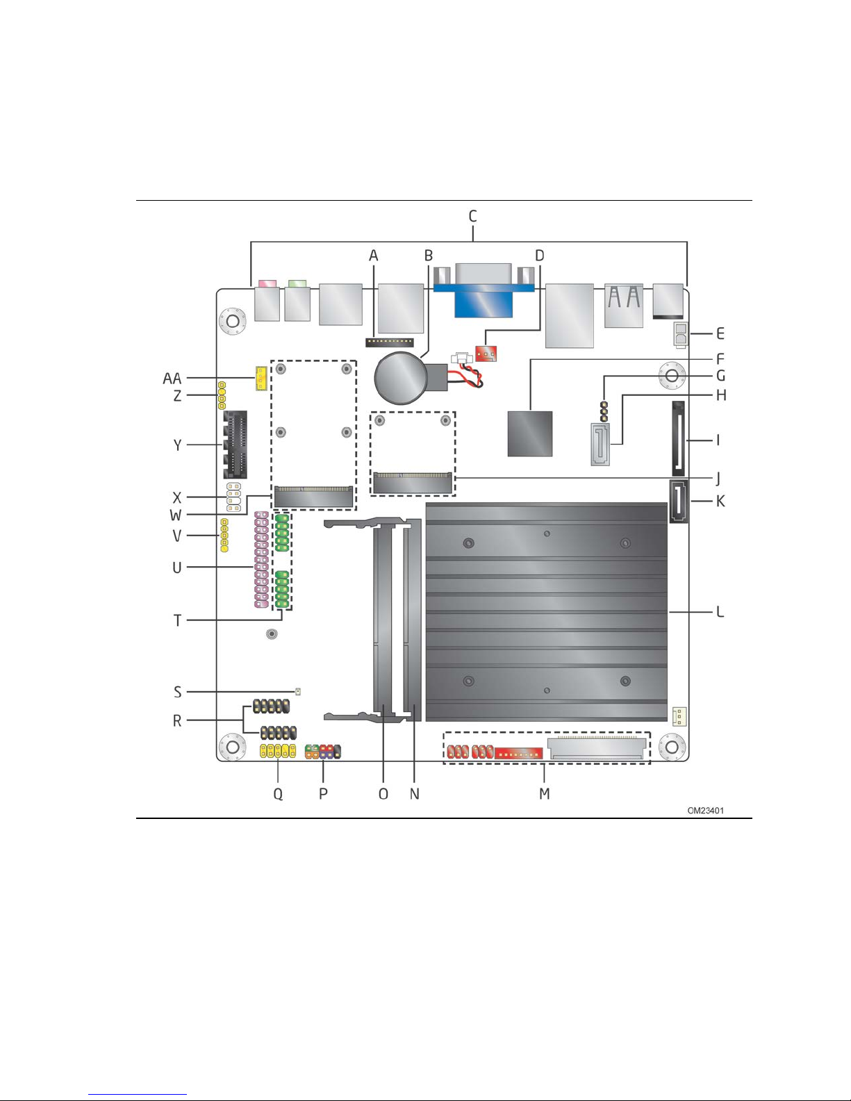
1.1.2 Board Layout (Top)
Figure 1 shows the location of the major components on the top-side of the Intel
Desktop Board DN2800MT.
Figure 1. Major Board Components (Top)
15
Page 16

Intel Desktop Board DN2800MT Technical Product Specification
Table 3 lists the components identified in Figure 1.
Table 3. Components Shown in Figure 1
Item/callout
from Figure 1 Description
A Debug connector
B Battery
C Back panel connectors
D System fan header
E Inter na l p ower connector
F Intel NM10 Express Chipset
G BIOS Setup configuration jumper b lock
H SATA data conne c to r
I SATA power connector
J PCI Express Half-Mini card slot
K S A T A d ata c o nne c tor
L Intel Atom processor and heatsink
M Flat panel display connectors
N DDR3 SO-DIMM 0 socket
O DDR3 SO-DIMM 1 socket
P Front panel header
Q Front panel audio heade r
R F ront panel dual-port USB headers
S Standby power LED
T Se r ia l p ort headers
U Parallel po rt header
V DMIC header
W PCI Express Full-/Half-Mini Card slot
X Custom Solutions header
Y PCI Express 1.0a x1 connector
Z S/PDIF header
AA Internal stereo speakers connector
16
Page 17
Product Description
1.1.3 Board Layout (Bottom)
Figure 2 shows the location of the major components on the bottom-side of the Intel
Desktop Board DN2800MT.
Figure 2. Major Board Components (Bottom)
Table 4. Components Shown in Figure 2
Item/callout
from Figure 2
A Embedded Display Port (eDP) connector
Description
17
Page 18
Intel Desktop Board DN2800MT Technical Product Specification
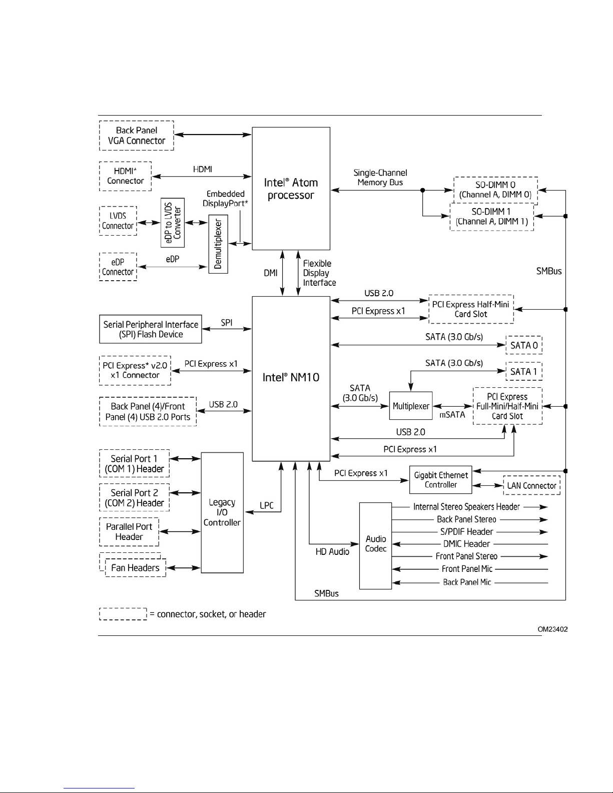
1.1.4 Block Diagram
Figure 3 is a block diagram of the major functional areas of the board.
18
Figure 3. Block Diagram
Page 19

1.2 Online Support
To find information about… Visit this World Wide Web site:
Intel Desktop Board DN2800MT http://www.intel.com/products/motherboard/index.htm
Desktop Board Support http://www.intel.com/p/en_US/support?iid=hdr+support
Available config ur a tio ns for Intel
Desktop Board DN2800MT
Chipset informatio n http://www.intel.com/products/desktop/chipsets/index.htm
BIOS and driver updates http://downloadcenter.intel.com
Tested memory http://www.intel.com/support/motherboards/desktop/sb/CS-
Integration info r m ation http://www.intel.com/support/go/buildit
1.3 Processor
Product Description
http://ark.intel.com
025414.htm
The board has a fanlessly-cooled, soldered-down dual-core Intel Atom processor
N2800 with integrated graphics and integrated memory controller.
NOTE
The board is designed to be fanlessly cooled in a properly ventilated chassis. Chassis
venting locations are recommended above and next to the processor area for
maximum heat dissipation effectiveness.
19
Page 20

Intel Desktop Board DN2800MT Technical Product Specification
1.4 System Memory
The board has two 204-pin SO-DIMM sockets and supports the following memory
features:
• 1.5 V DDR3-800 and DDR3-1066 SO-DIMMs with gold-plated contacts
• Unbuffered, non-ECC, Raw Card B (1Rx8) and Raw Card-F (2Rx8) SO-DIMMs only
• Single-sided or double-sided modules
• 4 GB maximum total system memory
• Serial Presence Detect
• DDR3 800 MHz and DDR3 1066 MHz SO-DIMMs
(Higher speed SO-DIMMs supported at 1066 MHz if supported by the memory
module.)
NOTES
• Due to fanless thermal constraints, system memory must have an operating
temperature rating of 85
The board is des igned to be fanlessly cooled in a properly ventilated chassis.
Chassis venting locations are recommended above the system memory area for
maximum heat dissipation effectiveness.
• If you are installing only one SO-DIM M, it must be installed in the bottom socket
(SO-DIMM 1).
• To be fully compliant with all applicable DDR SDRAM memory specifications , the
board should be populated with SO-DIMMs that support the Serial Presence Detect
(SPD) data structure. This allows the BIOS to read the SPD data and program the
chipset to accurately configure memory settings for optimum performance. If nonSPD memory is installed, the B I OS will attempt to correctly configure the memory
settings, but perfo rmance and reliability may be impacted or the SO-DIMMs may
not function under the determined frequency.
o
C.
20
Page 21
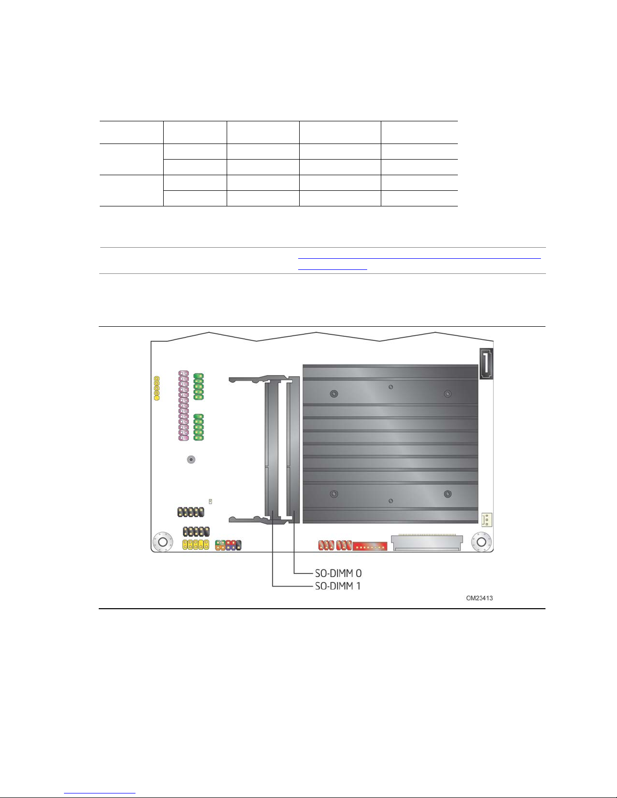
Table 5 lists the supported SO-DIMM configurations.
Version
Capacity
Technology
Organization
Devices
Table 5. Supported Memory Configurations
Raw Card
SO-DIMM
DRAM Device
DRAM
Product Description
# of DRAM
B
F
Note: System memory conf i g urations are based on availability and are subject to change.
1 GB 1 Gb 128 M x 8 8
2 GB 2 Gb 256 M x 8 8
2 GB 1 Gb 128 M x 8 16
4 GB 2 Gb 256 M x 8 16
For information about… Refer to:
Tested Memory http://support.intel.com/support/motherboards/desktop/sb
/CS-025414.htm
Figure 4 illustrates the SO-DIMM configuration.
Figure 4. SO-DIMM Configuration
21
Page 22

Intel Desktop Board DN2800MT Technical Product Specification
1.5 Intel
Intel NM10 Express Chipset with Direct Media Interface (DMI) interconnect provides
interfaces to the processor and the USB, SATA, LPC, LAN, and PCI Express interfaces.
The Intel NM10 Express Chipset is a centralized controller for the board’s I/O paths.
For information about Refer to
The Intel NM10 chipset http://www.intel.com/products/desktop/chipsets/index.htm
Resources used by the chipset Chapter 2
®
NM10 Express Chipset
1.6 Graphics Subsystem
The board support s graphics through Intel Graphics Technology.
1.6.1 Integrated Graphics
The board support s integrated graphics through the Intel® Flexible Display Interface
®
(Intel
NOTE
The board can simultaneously support up to two of the three integrated graphics
interfaces: VGA, HDMI, and Flat Panel Display.
FDI) for processors with Intel Graphics Technology.
Flat Panel Display is supported by eDP and LVDS interfaces, however only one can be
used at a time.
1.6.1.1 Intel
The Intel® GMA graphics controller features the following:
• 640 MHz core frequency
• Video
Blu-ray* 2.0
PAVP 1.1c
HDCP 1.3
• Display
Supports VGA displays up to 1920 x 1200 (WUXGA) at 60 Hz
Supports HDMI displays up to 1920 x 1200 (WUXGA) at 60 Hz
Supports eDP or LVDS internal flat panel displays up to 1920 x 1080 at 60 Hz
Dual independent display support
For information about Refer to
Obtaining graphics s oftware and utilities Section 1.2, page 19
®
High Definition (Intel® HD) Graphics
22
Page 23

Product Description
1.6.1.2 Video Memory Allocation
Intel® Dynamic Video Memory Technology (DVMT) is a method for dynamically
allocating system memory f or use as graphics me m ory to balance 2D/3D gra phics and
system performance. If your computer is configured to use DVMT, graphics memory is
allocated based on system requirements and application demands (up to the
configured maximum amount). When memory is no longer needed by an application,
the dynamically allocated portion of memory is returned to the operating system for
other uses.
1.6.1.3 High Definition Multimedia Interface* (HDMI*)
The HDMI por t supports standard, enhanced, or high definition video, plus multichannel digital audio on a single cable. It is compatible with all ATSC and DVB HDTV
standards and supports eight full range channels at 24-bit/96 kHz audio. The
maximum supported resolution is 1920 x 1200 (WUXGA). The HDMI port is compliant
with the HDMI 1.3a specification.
Depending on the type of a d d-in card installed in the PCI Express x1 connector, the
HDMI port will behave as described in Table 6.
Table 6. HDMI Port Status Conditions
PCI Express x1 Connector Status HDMI Port Status
No add-in card installed Enabled
Non-video PCI Express x1 a dd-in card installed Enabled
Video PCI Express x1 add-in card installed Disabled
1.6.1.4 Analog Display (VGA)
The VGA port supports analog displays. The maximum supported resolution is 1920 x
1200 (WUXGA) at a 60 Hz refre sh rate.
23
Page 24
Intel Desktop Board DN2800MT Technical Product Specification
1.6.2 Flat Panel Display Interfaces
The board support s flat panel display via the LVDS and Embedded DisplayPort
interfaces. Figure 5 shows the flat panel connectors.
Item Description
A Backlight inverter voltage selection header
B Flat panel voltage se le c tion header
C FPD brightness conne c tor
D LV DS connector
E Embed d e d DisplayPort conne c to r
24
Figure 5. Flat Panel Connectors
Page 25

Product Description
1.6.2.1 LVDS Interface
The LVDS flat panel display interface supports the f ollowing:
• 1920 x 1080 @ 60 Hz resolution
• Single-channel and dual-channel interface, up to 135 MHz clock rate 18 bpp and
24 bpp (VESA* and JEIDA mappings) color depth support
• Multiple EDID data source capability (panel, predefined, and custom payloads)
• 3.3 V, 5 V, and 12 V flat panel display voltage flexibility, with up to 3 A current
• 5 V, 12 V and Vin backlight inverter voltage flexibility, with up to 3 A current
• Backlight inverter signal redundancy on dedicated header as well as on LVDS
connector (for discrete inverter or panel-integrated inverter support using a single
cable)
• Flat panel brightness control via front panel button input as well as Windows* 7
“Screen brightness” adjustment slider
• Spread-spectrum control
NOTE
Backlight inverter voltage option “Vin” re fers to board input v oltage as provide d to
board power input connector.
1.6.2.2 Embedded DisplayPort (eDP) Interface
The eDP (Embedded DisplayPort) flat panel display interface supports the following:
• 1920 x 1080 @ 60 Hz resolution
• 1-lane, 2-lane, and 4-lane bandwidth at 1.62 Gb/s or 2.7 Gb/s
• Multiple EDID data source capability (panel, predefined, and custom payloads)
• 3.3 V, 5 V, and 12 V flat panel display voltage flexibility, with up to 3 A current
• 5 V, 12 V and Vin backlight inverter voltage flexibility, with up to 3 A current
• Backlight inverter signal redundancy on a dedicated header as well as on eDP
connector (for discrete inverter or panel-integrated inverter support using a single
cable)
• Flat panel brightness control via front panel button input as well as Windows 7
“Screen brightness” adjustment slider
NOTE
Backlight inverter voltage option “Vin” re fers to board input v oltage as provide d to
board power input connector.
1.6.2.3 Configuration Modes
Video mode configuration for eDP/LVDS displays is supported as follows:
• Automatic panel identification via Extended Display Identification Data (EDID) for
panels with onboard EDID support
• Panel selection from common predefined panel types (without onboard EDID)
• Custom EDID payload installation for ultimate paramet er flexibility, allowing
custom definition of EDID d a ta on panels without onboard EDID
25
Page 26

Intel Desktop Board DN2800MT Technical Product Specification
In addition, BIOS setup pr ovides the following configuration parameters for internal
flat panel displays:
• Screen Brightness: allows the end user to set the screen brightness for the display
effective through the Power-On Self Test stage (such as while showing the splash
screen image and BIOS setup). Windows 7 will ignore this setting in favor of the
native “screen brightness” control provided by the operating syste m .
• Flat Panel Configuration Changes Lock: allows the system integrator to “lock”
critical settings of the LVDS configuration to avoid end users potentially rendering
the display unusable.
• Brightness Steps: allows the system integrator to configure the brightness steps for
the operating system’s “screen brightness” control (such as the “Screen brightness”
adjustment slider under the Windows 7 “Power Options” control panel).
• LVDS Interface Type: allows the system integrator to select whether the LVDS
panel is a single-channel or dual-channel display.
• Swap LVDS Channels 0/1: allows the system integrator to swap the EVEN/ODD
LVDS channel assignments shall the cable be wired opposite the panel pinout.
• Color Depth: allows the system integrator to select whether the panel is 24 bpp
with VESA color mapping (eDP and LVDS), 24 bpp with JEIDA color mapping (LVDS
only), or 18 bpp (eDP and LVDS).
• eDP Interface Type: allows the system integrator to select whether the eDP panel is
a 1-lane, 2-lane, or 4-lane display.
• eDP Data Rate: allows the system integrator to select whether the eDP panel runs
at 1.62 Gb/s or 2.7 Gb/s.
• Inverter Frequency and Polarity: allows the system integrator to set the operating
frequency and polarity of the panel inverter board.
• Maximum and Minimum Inverter Current Limit (%): allows the system integrato r to
set maximum PWM%, as appropriate, according to the power requirements of the
internal flat panel display and the selected inverter board.
• Panel Power Sequencing: allows the system integrator to adjust panel sequencing
parameters, if necessary.
• LVDS Spread Spectrum Control: allows the system integrator to adjust spread
spectrum for the LVDS interface.
NOTE
Support for flat panel display configuration complies with the following:
1. Internal flat panel display connec tivity is disabled (and all parameters hidden) by
default.
2. Internal flat panel display settings are not exposed through Intel
Toolkit or Intel
3. Internal flat panel display settings will not be overwritten by loading BIOS setup
defaults.
4. Internal flat panel display settings will be preserved across BIOS updates.
26
®
Integrator Assis tant GUIs.
®
Integrator
Page 27

Product Description
1.6.3 USB
The board support s up to ten USB ports. The port arrangement is as follows:
• Four front panel ports (via two internal headers; one header supports an Intel
Z-U130 USB Solid-State Drive (or compatible device))
• Two ports are implemented with stacked back panel connectors (black)
• Two high-current/fast-charging ports are implemented through stacked back p a nel
connectors (yellow)
• One port implemented in the PCI Express Half–Mini Card slot
• One port implemented in the PCI Express Full-/Half-Mini Card slot
The USB controller on the Intel NM10 Express Chipset provides a direct logical
connection to the USB ports on the back panel as well as on the PCI Express Mini Card
slots, and an indirect connection (through onboard USB hub) to the interna l USB
headers. All ten USB ports are high-speed, full-speed, and low-speed capable.
NOTE
Computer systems that have an unshielded cable attached to a USB port ma y not meet
FCC Class B requirements, even if no device is attached to the cable. Use a shielded
cable that meets the requirements for full-speed devices.
For information about Refer to
The location of the USB c onnectors on the back panel Figure 12, page 46
The location of the front panel USB headers Figure 13, page 47
®
27
Page 28

Intel Desktop Board DN2800MT Technical Product Specification
1.7 SATA Interfaces
The board provides two SATA ports through the PCH, which support one device per
port:
• One internal SATA connector (black)
• One internal SATA connector (multiplexed with mSATA port , routed to PCI Express
Full-/Half-Mini Card slot) (gray)
The PCH provides independent SATA ports with a theoretical maximum transfer rate of
3 Gb/s. A point-to-point interface is used for host to device connections.
The underlying SATA functionality is transparent to the operating system. The SATA
controller can operate in both legacy and native modes. In legacy mode, standard IDE
I/O and IRQ resources are assigned (IRQ 14 and 15). In Native mode, standard PCI
Conventional bus resource steering is used. Native mode is the preferred mode for
configurations using Windows operating systems.
The board has an internal SATA power connector and ships with a power cable for
powering internal SATA storage devices. The power cable includes:
• Right-angled 15-pin SATA female connector (for motherboard connectivity)
• 1 x 4 Molex female connector (for slim optical drive adapter connectivity)
• 15-pin SATA female connector (for storage connectivity)
• Vertical 15-pin SATA female connector (for storage connectivity)
NOTE
Board power supplied through the SATA power connector is rated a t a ma ximum of:
• 1.0 A from 12 V rail
• 2.5 A from 5 V rail
• 0.5 A from 3.3 V rail
For information about Refer to
The location of the SA TA c onnectors Figure 13, page 47
1.7.1 AHCI Mode
The board support s AHCI storage mode via the Intel NM10 Express Chipset.
NOTE
In order to use AHCI mode, AHCI must be enabled in the BIOS. Microsoft Windows 7
includes the necessary AHCI drivers without the need to install separate AHCI drivers
during the operating system installation process, however, it is always good practice to
update the AHCI drivers to the latest available release.
28
Page 29

Product Description
1.8 Real-Time Clock Subsystem
A coin-cell battery (CR2032) powers the real-time clock and CMOS memory. When the
computer is not plugged into a wall socket, the battery has an estimated life of three
years. When the computer is plugged in, the standby current from the po w er supply
extends the life of the battery. The clock is accurate to ± 13 minutes/year at 25 ºC
with 3.3 VSB applied via the power supply 5 V STBY rail.
NOTE
If the battery and AC po w er fail, date and time values will be reset and the user will be
notified during the POST.
When the voltage drops below a certain level, the BIOS Setup program settings stored
in CMOS RAM (for example, the date and time) might not be accurate. Replace the
battery with an equivalent one. Figure 1 on page 15 shows the location of the battery.
1.9 Legacy I/O Controller
The I/O controller provides the following features:
• Two serial port headers
• One parallel port header with output only, bi-directional and Enhanced Parallel Port
(EPP) support
• Serial IRQ interface compatible with serialized IRQ support for PCI systems
• Intelligent power management, including a programmable wake-up event interface
The BIOS Setup program provides configuration options for the I /O controller.
1.9.1 Serial Ports
The serial ports, are implemented as two 10-pin headers on the board. The serial
ports support data transfers at speeds up to 115.2 kbits/sec with BIOS support.
For information about Refer to
1.9.2 Parallel Port
The location of the serial port headers Figure 13, page 47
The parallel port is implemented as a 26-pin header on the board. Use the BIOS Setup
program to set the parallel port mode.
For information about Refer to
The location of the parallel port header Figure 13, page 47
29
Page 30

Intel Desktop Board DN2800MT Technical Product Specification
1.10 Audio Subsystem
The board support s Intel HD Audio via the Realtek ALC888S audio codec and the HDMI
interface. The audio subsystem supports the following features:
• Analog line-out (back panel jack)
• Analog line-in (back panel jack)
• In-chassis stereo speakers support (3 W/3 Ω via internal header)
• Signal-to-noise ratios (SNR) of 97 dB for the DACs and 90 dB for the ADCs
• Support for 44.1 kHz/48 kHz/96 kHz/192 kHz sample r ates on all analog outputs
• Support for 44.1 kHz/48 kHz/96 kHz sample rates on all analog inputs
• S/PDIF digital audio output (internal header)
• Support for 44.1 kHz/48 kHz/88.2 kHz/96 kHz/192 kHz sample rates at 16-bit,
20-bit or 24-bit resolution on SPDIF outputs
• DMIC interface (internal header), with support for mono and stereo digital
microphones
• Front panel HD Audio/AC’97 headphones/microphone support (internal header)
• Advanced jack sense for the back panel line-out jack that enables the audio codec
to recognize the connected device
• Microphone input jack that supports a single dynamic, condenser, or electret
microphone
• Windows 7 Ultimate certification
Table 7 lists the supported functions of the front panel and back panel audio jacks.
Table 7. Audio Jack Support
Audio Jack Microphone Headphones Line Out Line In
FP Green Jack Default
FP Pink Jack Default
Rear Green Jack Jack detect
Rear Pink Jack Default
Internal Stereo S p e a k e r Default
30
Page 31

Product Description
1.10.1 Audio Subsystem Software
The latest audio software and drivers are available from Intel’s World Wide Web site.
For information about Refer to
Obtaining audio sof tw a r e and drivers Section 1.2, page 19
1.10.2 Audio Subsystem Components
The audio subsystem includes the following components:
• Intel NM10 Express Chipset
• Realtek ALC888S audio codec
• Two ports for analog line-in and analog line-out on the back panel
• Front panel audio header that supports Intel HD audio and AC’97 a udio (a 2 x 5-pin
header that provides microphone in and headphones signals for front panel audio
connectors)
• Internal S/PDIF header (1 x 4-pin header)
• Internal DMIC header (1 x 5-pin header)
• Internal stereo speakers connector (1 x 4-pin, shrouded)
The back panel audio connectors are configurable through the audio device drivers.
The available configurable back panel audio connectors are shown in Figure 6.
Item Description
A Analog line out
B Analog line-in
Figure 6. Back Panel Audio Connectors
NOTE
The analog circuit of the back panel audio line out connector is designed to power
headphones or amplified speakers only. Poor audio quality occurs if passive (nonamplified) speaker s are connecte d to this output.
31
Page 32

Intel Desktop Board DN2800MT Technical Product Specification
Figure 5 shows the location of the internal audio headers.
32
Item Description
A Front panel audio he ad e r
B DMIC header
C S/PDIF header
D I nternal stereo speakers connector
Figure 7. Internal Audio Headers
For information about Refer to
The signal names of the audio headers Section 2.2.3.1, page 50
Page 33

1.11 LAN Subsystem
The LAN subsystem consists of the following:
• Intel 82574L Gigabit Ethernet Controller (10/100/1000 Mbits/s)
• Intel NM10 Express Chipset
• RJ-45 LAN connector w ith integrated status LEDs
For information about Refer to
LAN software and d rivers http://downloadcenter.intel.com
Product Description
1.11.1 Intel
The Intel 82574L Gigabit Ethernet Controller supports the fo llowing features:
• 10/100/1000 BASE-T (IEEE 802.3, 802.3u and 802.3ab) compliant
• IEEE 802.3ab auto negotiation support
• IEEE 802.3x flow control and Auto MDI, MDI-X crossover at all speeds
• Full wak e-up support (APM and ACPI 2 .0) (Magic Packet* wake-up capable)
• Smart power down at S0 no link and Sx no link
• Jumbo (9kB) frame support
• TimeSync offload (IEEE1588 and 802.1as) compliant
• Quality of Service (QoS) (802.1p) compliant
• VLAN (802.1q) compliant
• TCP, IP, and UDP checksum offload (for IPv4 and IPv6)
• Full device driver compatibility
®
82574L Gigabit Ethernet Controller
33
Page 34

Intel Desktop Board DN2800MT Technical Product Specification
1.11.2 LAN Subsystem Software
LAN software and drivers are available from Intel’s World Wide Web site.
For information about Refer to
Obtaining LAN softw are and drivers http://downloadcenter.intel.com
1.11.3 RJ-45 LAN Connector with Integrated LEDs
Two LEDs are built into the RJ-45 LAN connector (shown in Figure 8).
Item Description
A Link LED (Green)
B Data Rate LED (Green/Yell o w )
Figure 8. LAN Connector LED Locations
Table 8 describes the LED states w hen the board is powered up and the LAN
subsystem is opera ting.
Table 8. LAN Connector LED States
LED LED Color LED State Condition
Off LAN link is not establishe d .
Link Green
Data Rate Green/Yellow
On LA N link is e s tablished.
Blinking LAN activity is occurring.
Off 10 Mbits/s data rate is selected.
Green 100 Mbits/s data rate is selected.
Yellow 1000 Mbits/s data rate is selected.
34
Page 35

Product Description
1.12 Hardware Management Subsystem
The hardware management features enable the board to be compatible with the Wired
for Management (WfM) specification. The board has several hardware management
features, including thermal and voltage monitoring.
For information about Refer to
Wired for Manage me nt (WfM) Specification www.intel.com/design/archives/wfm/
1.12.1 Hardware Monitoring
The hardware monitoring and fan control subsystem is based on the Nuvoton
W83627DHG device, which supports the following:
• Processor and system ambient temperature monitoring
• System fan speed monitoring
• Voltage monitoring of +12 V, +5 V, +3.3 V, PCH Vcc, Memory Vcc, Processor Vcc
and +3.3V Standby
• SMBus interface
1.12.2 Fan Monitoring
Fan monitoring can be implemented using Intel® Desktop Utilities or third-party
software.
For information about Refer to
The functions of the f an he ader Section 1.13.2.2, page 40
35
Page 36

Intel Desktop Board DN2800MT Technical Product Specification
1.12.3 Thermal Monitoring
Figure 9 shows the locations of the thermal sensor and fan header.
Item Description
A System fan header
B Thermal diode, located on the processor die
Figure 9. Thermal Sensor and Fan Header
36
Page 37

Product Description
1.13 Power Management
Power management is implemented at several levels, including:
• Software support through Advanced Configuration and Power Interf ace (ACPI)
• Hardware support:
Power connector
Fan header
LAN wake capabilities
Instantly Available PC technology
Wake from USB
Wake from serial port
PCI Express WAKE# signal support
1.13.1 ACPI
ACPI gives the operating system direct control over the power management and Plug
and Play functions of a computer. The use of ACPI with this board r equires an
operating system that provides full ACPI support. AC PI features include:
• Plug and Play (including bus and device enumeration)
• Power management control of individual devices, add-in boards (some add-in
boards may require an ACPI-aware driver), video displays, and hard disk drives
• Methods for achieving less than 15-watt system operation in the power-on/standby
sleeping state
• A Soft-off feature that enables the opera t ing sy stem to power-off the computer
• Support for multiple wake-up events (see Table 11 on page 39)
• Support for a front panel power and sleep mode switch
Table 9 lists the system states based on how long the power switch is pressed,
depending on how ACPI is configured with an ACPI-aware operating system.
Table 9. Effects of Pressing the Power Switch
If the system is in this
state…
Off
(ACPI G2/G5 – Soft off)
On
(ACPI G0 – wo rking state)
On
(ACPI G0 – working state)
Sleep
(ACPI G1 – slee ping state)
Sleep
(ACPI G1 – slee ping state)
Note: Depending on p ower management settings in the operating sy s te m.
…and the power switch is
pressed for
Less than four seconds Power-on
Less than four seconds Soft-off/Standby
More than six second s Fail safe power-off
Less than four seconds Wake-up
More than six second s Power-off
…the system enters this state
(ACPI G0 – wo rking state)
(ACPI G1 – slee ping state)
(ACPI G2/G5 – Soft off)
(ACPI G0 – wo rking state)
(ACPI G2/G5 – Soft off)
Note
37
Page 38

Intel Desktop Board DN2800MT Technical Product Specification
1.13.1.1 System States and Power States
Under ACPI, the operating system directs all system and device power state
transitions. The opera ting sy stem puts devices in and out of low-power states based
on user preferences and knowledge of how devices are being used by applications.
Devices that are not being used can be turned off. The operating system uses
information from applications and user settings to put the system as a whole into a
low-power state.
Table 10 lists the power sta tes supported by the b oard along with the associated
system power targets. See the ACPI specification for a complete description of the
various system and power states.
Table 10. Power States and Targeted System Power
Global States Sleeping States
G0 – working
state
G1 – sleeping
state
G1 – sleeping
state
G2/S5 S5 – Soft off.
G3 –
mechanical off
AC power is
disconnected
from the
computer.
Notes:
1. To tal system power is d e p e ndent on the system configuration, including add-in boards and per ipherals
powered by the system chassis’ power supply.
2. D e p e ndent on the standby po w e r consumption of w ake-up devices used in the system.
S0 – working C0 – working D0 – working
S3 – Suspend to
RAM. Context
saved to RAM.
S4 – Suspend to
disk. Context
saved to disk.
Context not saved .
Cold boot is
required.
No power to the
system.
Processor
States
No power D3 – no power
No power D3 – no power
No power D3 – no power
No power D3 – no power for
Device States
state.
except for
wake-up logic.
except for
wake-up logic.
except for
wake-up logic.
wake-up logic,
except when
provided by
battery or
external source.
Targeted System
Power
Full power > 30 W
Power < 5 W
Power < 5 W
Power < 5 W
No power to the s y s te m .
Service can be performed
safely.
(Note 1)
(Note 2)
(Note 2)
(Note 2)
38
Page 39

Product Description
Note 1)
(Note 1)
(Note 3)
(Note 1)
(Note 3)
(Note 1)
(Note 3)
1.13.1.2 Wake-up Devices and Events
Table 11 lists the devices or specific events that can wake the computer from specific
states.
Table 11. Wake-up Devices and Events
Devices/events that wake up the system… …from this sleep state …from this global state
Power switch S3, S4, S5
RTC alarm S3, S4, S5
LAN S3, S4, S5
USB S3 G1
WAKE# S3, S4, S5
Serial port S3 G1
Notes:
1. S 4 im p lie s operating system s up port only.
2. Wake from S4 and S5 is recommended by Microsoft.
3. Wak e from device/event not supported im me diately upon return f rom AC loss.
(
G1, G2, G3
G1, G2
G1, G2
G1, G2
NOTE
The use of these wake-up events from an ACPI state requires an operating system that
provides full ACPI support. In addition, so ftware, drivers, and peripherals must fully
support ACPI wake events.
1.13.2 Hardware Support
The board provides several power management hardware features, including:
• Instantly Available PC technology
• Fan headers
• LAN wake capabilities
• Wake from USB
• WAKE# signal wake-up support
• Wake from serial port
• Wake from Power Button signal
• Standby Power Indicator LED
NOTE
The use of Wake from USB from an ACPI state requires an operating system that
provides full ACPI support.
39
Page 40

Intel Desktop Board DN2800MT Technical Product Specification
1.13.2.1 Power Input
When resuming from an AC power failure, the computer returns to the power state it
was in before power was interrupted (on or off). The computer’s response can be set
using the Last Power State feature in the BIOS Setup program’s Boot menu.
For information about Refer to
The location of the internal power connector Figure 13, page 47
The signal names of the internal power connector Table 34, page 58
1.13.2.2 Fan Header
The function/operation of the fan header is as follows:
• The fan is on when the board is in the S0 s ta te
• The fan is off when the board is off or in the S3, S4, or S5 state.
• The fan header is wired to a fan tachometer input of the hardware monitoring and
fan control ASIC.
• The fan header supports closed-loop fan control that can adjust the fan speed as
needed.
• The fan header has a +12 V DC connection.
• The fan header supports 3-wire (voltage controlled) fans.
For information about Refer to
The location of the fan he a d e r Figure 13, page 47
The location of the fan he a d e r and sensor for thermal monitoring Figure 9, page 36
40
Page 41

Product Description
1.13.2.3 LAN Wake Capabilities
LAN wake capabilities enable remote wake-up of the computer through a network. The
LAN subsystem monitors network traffic at the Media Independent Interface. Upon
detecting a Magic Packet* f rame, the LAN subsystem asserts a w ake-up signal that
powers up the computer.
1.13.2.4 Instantly Available PC Technology
Instantly Available PC technology enables the board to enter the ACPI S3 (Suspend-toRAM) sleep-state. While in the S3 sleep-state, the computer will appear to be off (the
power supply is off, and the front panel LED is amber if dual colored, or off if single
colored.) When signaled by a w ake-up device or event, the system quickly returns to
its last known wake state. Table 11 on page 39 lists the devices and events that can
wake the computer from the S3 state.
The use of Instantly Available PC technology requires operating system support and
drivers for any installed PCI Express add-in card.
1.13.2.5 Wake from USB
USB bus activity wakes the computer from an ACPI S3 state.
NOTE
Wake from USB requires the use of a USB peripheral that supports Wake from USB.
1.13.2.6 WAKE# Signal Wake-up Support
When the WAKE# signal on the PCI Express bus is asserted, the computer wakes from
an ACPI S3, S4, or S5 state.
1.13.2.7 Wake from Serial Port
Serial Port activity wakes the computer from an ACPI S3 state.
1.13.2.8 Wake from S5
When the RTC Date and Time is set in the BIOS, the computer will automatically w ake
from an ACPI S5 state.
41
Page 42

Intel Desktop Board DN2800MT Technical Product Specification
1.13.2.9 Standby Power Indicator LED
The standby power indicator LED shows that power is still present even when the
computer appears to be off. Figure 10 shows the location of the standby power LED .
CAUTION
If AC power has been switched off and the standby power indicator is still lit,
disconnect the power cord before installing or removing any devices connected to the
board. Failure to do so could damage the board and any attached devices.
Figure 10. Location of the Standby Power LED
42
Page 43

2 Technical Reference
2.1 Memory Resources
2.1.1 Addressable Memory
The board utilizes 4 GB of addressable system memory. Typically the address space
that is allocated for PCI Conventional bus add-in cards, PCI Express configuration
space, BIOS (SPI Flash device), and chipset overhead resides above the top of DRAM
(total system memory). On a system that has 4 GB of system memory installed, it is
not possible to use all of the installed memory due to system a dd ress space be ing
allocated for other system critical functions. These functions include the following:
• BIOS/SPI Flash device (2 Mbit)
• Local APIC (19 MB)
• Direct Media Interface (40 MB)
• PCI Express configuration space (256 MB)
• PCH base address registers
• PCI Expres s ports (up to 256 MB)
• Memory-mapped I/O that is dynamically allocated for PCI Express add-in cards
(256 MB)
The board provides the capability to reclaim the physical memory overlapped by the
memory mapped I/O logical address space. The board remaps physical memory from
the top of usable DRAM bo undary to the 4 GB boundary to an equivalent sized logical
address range located just above the 4 GB boundary. Figure 11 shows a schematic of
the system memory map. All installed system memory can be used when there is no
overlap of system addresses.
43
Page 44

Intel Desktop Board DN2800MT Technical Product Specification
Figure 11. Detailed System Memory Address Map
44
Page 45

2.1.2 Memory Map
Table 12 lists the system memory map.
Table 12. System Memory Map
Address Range
(decimal)
1024 K - 4194304 K 100000 - FFFFFFFF 4095 MB Extended memory
960 K - 1024 K F0000 - FFFFF 64 KB Runtime BIOS
896 K - 960 K E0000 - EFFFF 64 KB Reserved
800 K - 896 K C8000 - DFFFF 96 KB Potential available high DO S
640 K - 800 K A0000 - C7FFF 160 KB Video memory and BIOS
639 K - 640 K 9FC00 - 9FFFF 1 KB Extended BIOS data (movable by
512 K - 639 K 80000 - 9FBFF 127 KB Extended conve nti o nal me mory
0 K - 512 K 00000 - 7FFFF 512 KB Conve ntio na l me mory
Address Range
(hex)
Size
Technical Reference
Description
memory (open to the PC I bus).
Dependent on vid e o adapter used.
memory manager software)
2.2 Connectors and Headers
CAUTION
Only the following connectors and headers have overcurrent protection: back panel
and front panel USB.
The other internal connectors and headers are not overcurrent protected and should
connect only to devices inside the computer’s chassis, such as fans and internal
peripherals. Do not use these connectors or headers to power devices external to the
computer’s chassis. A fault in the load presented by the external devices could cause
damage to the computer, the power cable, and the external devices themselves.
Furthermore, improper connection of USB header single wire connectors may
eventually overload the overcurrent protection and cause damage to the board.
This section describes the board’s connectors and headers. The connectors and
headers can be divided into these groups:
• Back panel I/O connectors
• On-board I/O connectors and headers (see page 47 and page 49)
45
Page 46

Intel Desktop Board DN2800MT Technical Product Specification
2.2.1 Back Panel Connectors
Figure 12 shows the location of the back panel connectors for the board.
Item Description
A DC input jack
B USB ports
C LAN connector
D VGA connector
E High-current/fast charging USB ports
F HDMI connec tor
G Analog line out
H Microphone in
Figure 12. Back Panel Connectors
46
Page 47

Technical Reference
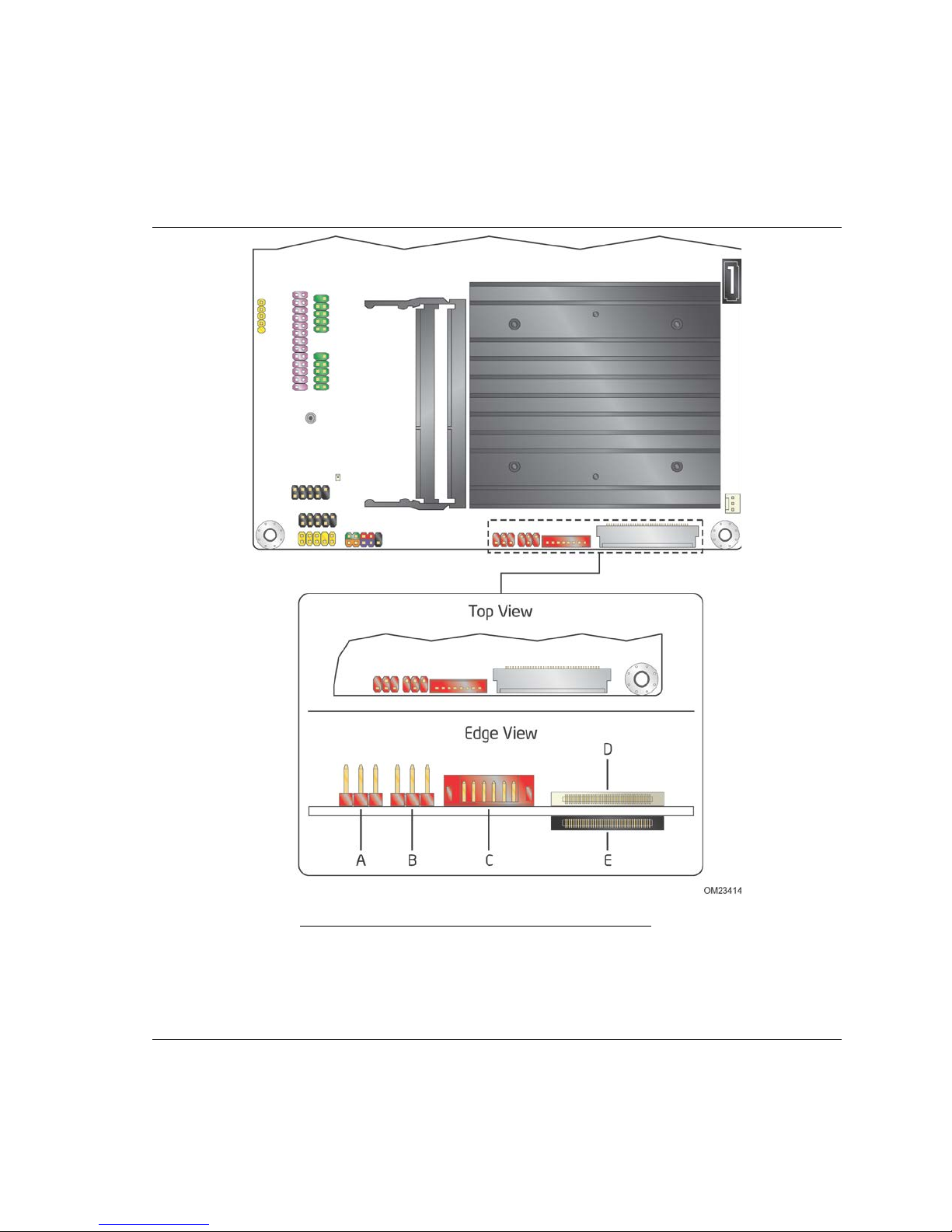
2.2.2 Connectors and Headers (Top)
Figure 13 shows the locations of the connectors and header s on the top-side of the
board.
Figure 13. Connectors and Headers (Top)
47
Page 48

Intel Desktop Board DN2800MT Technical Product Specification
header
Table 13 lists the connectors and headers identified in Figure 13.
Table 13. Connectors and Headers Shown in Figure 13
Item/callout
from Figure 13 Description
A Debug connector 1x11, 1.25mm-pitch
B System fan header 3-wire fan
C Internal power connector Molex* 5566-2 Molex 5557-02R
D SATA data connector 7-pin SATA (male) 7-pin SATA (female)
E SATA power connector 15-pin SATA (male) 15-pin SATA (female)
F PCI Express Half-Mini Card slot
G SATA data connector 7-pin SATA (male) 7-pin SA TA (female)
H LVDS connector ACES* 88341-40 ACES 88441-40
I FPD brig htne s s c onnector Foxconn* HF5508 JWT* A2001H02-8P
J Flat panel voltage se le c tion header 2x3, 2.54mm-pitch Jumper
K Backlight inv e rter voltage sele c tio n
Board Connector Mating Plug
2x3, 2.54mm-pitch Jumper
Connector Information
Starconn* 107F40
L Fr ont panel header 2x5, 2.54mm-pitch
M Front panel audio header 2x5, 2.54mm-pitch
N Front panel dual-port USB header 2x5, 2.54mm-pitch
O Front pane l d ual-por t USB header 2x5, 2.54mm-pitch
P S e rial port header 2x5, 2.54mm-pitch
Q Serial port header 2x5, 2.54mm-pitch
R Parallel port header 2x13, 2.54mm-pitch
S DMIC header 1x5, 2.54mm-pitch
T PCI Express Full-/Half-Mini Card slot
U Custom So lutions header 2x4, 2.00mm-pitch
V PCI Express 1.0a x1 connector
W S/PDIF header 1x4, 2.54mm-pitch
X Internal stereo speakers header JS*-1125-04 JWT* A2001H02-4P
48
Page 49

Technical Reference
2.2.3 Connectors and Headers (Bottom)
Figure 14 shows the lo cations of the connectors and headers on the bottom-side of the
board.
Figure 14. Connectors and Headers (Bottom)
Table 14 lists the connectors and headers identified in Figure 14.
Table 14. Connectors and Headers Shown in Figure 14
Item/callout
from Figure 14
A eDP connector ACES 50203-040 ACES 88441-40
Description
Board Connector Mating Plug
Connector In formation
Starconn 107F40
49
Page 50

Intel Desktop Board DN2800MT Technical Product Specification
2.2.3.1 Signal Tables for the Connectors and Headers
Table 15. Front Panel Audio Header for Intel HD Audio
Pin Signal Name Description
1 PORT_1L Analog Port 1 – Le f t c ha nne l (Mic r ophone)
2 GND Ground
3 PORT_1R Analog Port 1 – Right c hanne l (Microphone)
4 PRESENCE# Active low signal that si g nals B IOS that an Intel HD Aud io
dongle is connecte d to the analog header. PRESENCE#=0
when an Intel HD Audio d o ngle is connected
5 PORT_2R Analog Port 2 – Right c hanne l (He ad phone)
6 SENSE1_RETURN Jack detection r e turn for front p ane l (JA C K1)
7 SENSE_SEND Jack detection s e ns e line from the Intel HD Audio CODEC
jack detection resistor network
8 KEY No pin
9 PORT_2L Analog Port 2 – Le f t c ha nne l (He ad phone)
10 SENSE2_RETURN Jack detection re turn for front pa ne l (JA C K2)
Table 16. Front Panel Audio Header for AC’97 Audio
Pin Signal Name Description
1 MIC Front panel microphone inp ut s ig nal (b ias e d when
supporting ster e o microphone)
2 AUD_GND Gr o und used by analog audio circuits
3 MIC_BIAS Microphone pow e r / additional MIC input f or stereo
microphone supp ort
4 PRESENCE# Active low signal that si g nals B IOS that an Intel HD Aud io
dongle is connecte d to the analog header. PRESENCE#=0
when an Intel HD Audio d o ngle is connected
5 FP_OUT_R Right channel audio signal to front panel (headpho ne d rive
capable)
6 AUD_GND Gr o und used by analog audio circuits
7 RESERVED Reserved
8 KEY No pin
9 FP_OUT_L Left channel audio signal to front pane l (he adphone drive
capable)
10 AUD_GND Gro und us e d by analog audio circuits
50
Page 51

Table 17. Internal Stereo Speakers Header
Pin Signal Name Description
1 Front_L− Analog front left (diffe rential negative)
2 Front_L+ Analog front left (diffe rential positive)
3 Front_R+ Analog front right (differe ntial positive)
4 Front_R− Analog front right (differe ntial ne gative)
Table 18. Internal S/PDIF Header
Pin Signal Name Description
1 GND Ground
2 SPDIF_OUT SPDIF signal from the codec
3 Key (no pin) Key (no pin)
4 +5V_DC 5 V p o wer (for optic al/TOSLINK module)
Technical Reference
Table 19. Internal DMIC Header
Pin Signal Name Description
1 +3.3 V 3.3 V power (for DMIC module)
2 DMIC_DATA DMIC data signal
3 GND Ground
4 DMIC_CLK DMIC cloc k s ignal
5 Key (no pin) Key (no pin)
Table 20. Front Panel USB Dual-Port Header
Pin Signal Name Pin Signal Name
1 +5 V DC 2 +5 V DC
3 D− 4 D−
5 D+ 6 D+
7 Ground 8 Ground
9 KEY (no pin) 10 No Connect
Table 21. Front Panel USB Dual-Port Header (with support for Intel Z-U130
USB Solid-State Drive or compatible device)
Pin Signal Name Pin Signal Name
1 +5 V DC 2 +5 V DC
3 D− 4 D−
5 D+ 6 D+
7 Ground 8 Ground
9 KEY (no pin) 10 LED#
51
Page 52

Intel Desktop Board DN2800MT Technical Product Specification
Table 22. Serial Port Headers
Pin Signal Name Pin Signal Name
1 DCD (Data Carrier Detect) 2 RXD# (Receive Data)
3 TXD# (Trans m it D a ta) 4 DTR (D ata Terminal Ready)
5 Ground 6 DSR (Data Set Ready)
7 RTS (R e q ue s t T o S e nd) 8 CTS (Clear To Send)
9 RI (Ring Indicator) 10 Key (no p in)
Table 23. Parallel Port Header
Pin Standard Signal Name EPP Signal Name
1 STROBE# WRITE#
2 AUTOFD# DATASTB#
3 PD0 PD0
4 FAULT# FAULT#
5 PD1 PD1
6 INT# RESET#
7 PD2 PD2
8 SLCTIN# ADDRSTB#
9 PD3 PD3
10 GROUND GROUND
11 PD4 PD4
12 GROUND GROUND
13 PD5 PD5
14 GROUND GROUND
15 PD6 PD6
16 GROUND GROUND
17 PD7 PD7
18 GROUND GROUND
19 ACK# INTR
20 GROUND GROUND
21 BUSY WAIT#
22 GROUND GROUND
23 PERROR PE
24 GROUND GROUND
25 SELECT SELECT
26 KEY (no p in) KEY (no pin)
52
Page 53

Table 24. SATA Connectors
Pin Signal Name
1 Ground
2 TXP
3 TXN
4 Ground
5 RXN
6 RXP
7 Ground
Table 25. SATA Power Connector
Pin Signal Name
1 3.3 V DC
2 3.3 V DC
3 3.3 V DC
4 Ground
5 Ground
6 Ground
7 5 V DC
8 5 V DC
9 5 V DC
10 Ground
11 Ground
12 Ground
13 12 V DC
14 12 V DC
15 12 V DC
Technical Reference
Table 26. Custom Solutions Header
Pin Signal Name
1 Watch Dog Tim e r
2 Ground
3 Key (no pin)
4 SMB_CLK_RESUME
5 3.3 V stand by
6 SMB_DATA_RESUME
7 PWRBT#
8 HDMI CEC
53
Page 54

Intel Desktop Board DN2800MT Technical Product Specification
Table 27. System Fan Header
Pin Signal Name
1 Ground
2 +12 V (PWM c o ntrolled pulses)
3 Tach
Table 28. Flat Panel Voltage Selection Header
Pin Signal Name Description
1 Key No pin
2 3.3 V 3.3 V option (d e f a ult)
3 12 V 12 V o p tion
4 LCD_VCC Send voltage to connec tor
5 Key No pin
6 5 V 5 V option
Table 29. Backlight Inverter Voltage Selection Header
Pin Signal Name Description
1 Key No pin
2 5 V 5 V option
3 Vin B oard input voltage option
4 BKLT_PWR Send volta g e to connector
5 Key No pin
6 12 V 12 V o p tion
54
Page 55

Table 30. 40-Pin LVDS Connector
Pin Signal Name Pin Signal Name
1 ODD_Lane3_P 21 N/C
2 ODD_Lane3_N 22 EDID_3.3 V
3 ODD_Lane2_P 23 LCD_GND
4 ODD_Lane2_N 24 LCD_GND
5 ODD_Lane1_P 25 LCD_GND
6 ODD_Lane1_N 26 ODD_CLK_P
7 ODD_Lane0_P 27 ODD_CLK_N
8 ODD_Lane0_N 28 BKLT_GND
9 EVEN_Lane3_P 29 BKLT_GND
10 EVEN_Lane3_N 30 BKLT_GND
11 EVEN_Lane2_P 31 EDID_CLK
12 EVEN_Lane2_N 32 BKLT_ENABLE
13 EVEN_Lane1_P 33 BKLT_PWM_DIM
14 EVEN_Lane1_N 34 EVEN_CLK_P
15 EVEN_Lane0_P 35 EVEN_CLK_N
16 EVEN_Lane0_N 36 BKLT_PWR
17 EDID_GND 37 BKLT_PWR
18 LCD_VCC 38 BKLT_PWR
19 LCD_VCC 39 N/C
20 LCD_VCC 40 EDID_DATA
Technical Reference
NOTE
Single-channel LVDS panels m ust be wired to the “EVEN” channel of the LVDS
connector on initial revisions of the Intel Desktop B oard DN2800MT (G23738-600 and
earlier), as opposed to the “ODD” channel expected by single-channel LVDS designs.
A future motherboard revision (G23738-800 and later) is planned to support singlechannel LVDS con nectivity out o f the “ODD” channel.
Intel reco m mends that customers planning to use single-channel LVDS panels ensu re
cable wiring matches the target board revision.
55
Page 56

Intel Desktop Board DN2800MT Technical Product Specification
Table 31. 40-Pin eDP Connector
Pin Signal Name Pin Signal Name
1 NC_Reserved 21 LCD_VCC
2 High-speed_GND 22 LCD_Self_Test-or-NC
3 Lane3_N (DDPD_[3]N) 23 LCD_GND
4 Lane3_P (D DPD_[3]P) 24 LCD_GND
5 High-speed_GND 25 LCD_GND
6 Lane2_N (DDPD_[2]N) 26 LCD_GND
7 Lane2_P (D DPD_[2]P) 27 HPD (DDPD_HPD)
8 High-speed_GND 28 BKLT_GND
9 Lane1_N (DDPD_[1]N) 29 BKLT_GND
10 Lane1_P (DDPD_[1]P) 30 BKLT_GND
11 High-speed_GND 31 BKLT_GND
12 Lane0_N (DDPD_[0]N) 32 BKLT_ENABLE
13 Lane0_P (DDPD_[0]P) 33 BKLT_PWM_DIM
14 High-speed_GND 34 NC_Reserved
15 AUX_CH_P (DDPD_AUXP) 35 NC_Reserved
16 AUX_CH_N (DDPD_AUXN) 36 BKLT_PWR
17 High-speed_GND 37 BKLT_PWR
18 LCD_VCC 38 BKLT_PWR
19 LCD_VCC 39 BKLT_PWR
20 LCD_VCC 40 NC_Reserved
Table 32. 8-Pin FPD Brightness Connector
Pin Signal Name Description
1 BKLT_EN Backlight enab l e
2 BKLT_PWM B ac klight control
3 BKLT_PWR Backlight inverter pow e r
4 BKLT_PWR Backlight inverter pow e r
5 BKLT_GND/Brightness_GND Ground (shared)
6 BKLT_GND/Brightness_GND Ground (shared)
7 Brightness_Up Panel brightness increase
8 Brightness_Down Panel brightness decrease
56
Page 57

Table 33. PCI Express Full-/Half-Mini Card Connector
Pin Signal Name Additional Signal Name
1 WAKE#
2 +3.3 V aux
3 Reserved
4 GND
5 Reserved
6 1.5 V
7 CLKREQ#
8 Reserved
9 GND
10 Reserved
11 REFCLK-
12 Reserved
13 REFCLK+
14 Reserved
15 GND
16 Reserved
17 Reserved
18 GND
19 Reserved
20 Reserved
21 GND
22 PERST#
23 PERn0
24 +3.3 V aux
25 PERp0
26 GND
27 GND
28 +1.5 V
29 GND
30 SMB_CLK
31 PETn0
32 SMB_DATA
33 PETp0
34 GND
35 GND
36 USB_D-
37 GND (mSATA) GND
38 USB_D+
continued
Technical Reference
57
Page 58

Intel Desktop Board DN2800MT Technical Product Specification
Table 33. PCI Express Full-/Half-Mini Card Connector (continued)
Pin Signal Name Additional Signal Name
39 +3.3 V aux (mSA T A ) 3 .3 V
40 GND
41 +3.3 V aux (mSA T A ) 3 .3 V
42 LED_WWAN#
43 Reserved NC (mSATA ind i c ato r)
44 LED_WLAN#
45 Reserved (mSATA) Vendor
46 LED_WPAN#
47 Reserved (mSATA) Vendor
48 +1.5V
49 Reserved (mSATA) DA/DSS
50 GND
51 Reserved (mSATA) Presence Detection
52 +3.3 V aux
2.2.3.2 Add-in Card Connectors
The board has the following add-in card connectors:
• One PCI Express 1.0a x1 connector. The x1 interface supports simultaneous
transfer speeds up to 250 MB/s of pea k bandwidth per lane, per direction, for up to
500 MB/s concurrent and bi-directional bandwidth.
• One PCI Express Half-Mini Card slot
• One PCI Express Full-/Half-Mini Card slot (removable stand-offs in full-length keep
out zone allows repurposing of Full-Mini Card slot into Half-Mini Car d slot)
2.2.3.3 Power Supply Connectors
The board supports wide-range voltage input by either of the following power supply
types:
• External Power Supply – the board can be powered with an 8 - 19 VDC external
power supply though the DC jack on the back panel. This connector accepts dua lbarrel plugs with an inner diameter (ID) of 2.5 mm and an outer diameter (OD) of
5.5 mm, where the inner contact is +8 (±10%) through +19 (±10%) VDC and the
shell is GND. The maximum current rating for this connector is 8 A.
• Internal Power Supply – the board can alternatively be powered via the internal
1 x 2 power connector, where pin 1 is GND and pin 2 is +8 (±10%) through +19
(±10%) VDC. The maximum current rating for this connector is 10 A.
Table 34. Internal Power Supply Connector Pinout
Pin Signal Name
1 Ground
2 DC input: +8 (±10%) through +19 (±10%) VDC
58
Page 59

Technical Reference
For information about Refer to
Power supply c o ns iderations Section 2.6.1, page 69
2.2.3.4 Front Panel Header
This section describes the functions of the front panel header. Table 35 lists the signal
names of the front panel header. Figure 15 is a connection diagram for the front panel
header.
Table 35. Front Panel Header
Pin Signal Name Description Pin Signal Name Description
1 HDD_POWER_LED Pull-up resistor
(750 Ω) to +5V
3 HDD_LED# [Out] Hard disk
activity LED
5 GROUND Ground 6 POWER_SWITCH# [In] Pow e r s witch
7 RESET_SWITCH# [In] Reset switch 8 GROUND Ground
9 +5V_DC Power 10 Key No pin
2 POWER_LED_MAIN [Out] F ront panel LED
(main color)
4 POWER_LED_ALT [Out] Front pa ne l LED
(alt color)
Figure 15. Connection Diagram for Front Panel Header
2.2.3.4.1 Hard Drive Activity LED Header
Pins 1 and 3 can be connected to an LED to provide a visual indicator that data is
being read from or written to a hard drive. Proper LED function requires a SATA hard
drive or optical drive connected to an onboard SATA connector.
59
Page 60

Intel Desktop Board DN2800MT Technical Product Specification
2.2.3.4.2 Reset Switch Header
Pins 5 and 7 can be connected to a momentary single pole, single throw (SPST) type
switch that is normally open. When the switch is closed, the board resets and runs the
POST.
2.2.3.4.3 Power/Sleep LED Header
Pins 2 and 4 can be c onnected to a one- or two-color LED. Table 36 shows the
possible LED states.
Table 36. States for a One-Color Power LED
LED State Description
Off Power off
Blinking Standby
Steady Normal o p e ration
NOTE
The LED behavior shown in Table 36 is default – other patterns may be set via BIOS
setup.
2.2.3.4.4 Power Switch Header
Pins 6 and 8 can be connected to a front panel momenta ry-contact power switch. The
switch must pull the SW_ON# pin to ground for a t lea st 50 ms to signal the switch on
or off. (The time requirement is due to internal debounce circuitry on the board.) At
least two seconds must pass before the board will recognize another on/off signal.
60
Page 61

Technical Reference
2.2.3.5 Front Panel USB Headers
Figure 16 is a connection diagram for the front panel USB headers.
NOTE
• The +5 V DC power on the USB headers is fused.
• Use only a front panel USB c onnector that conforms to the USB 2.0 specification for
high-speed USB devices.
Figure 16. Connection Diagram for Front Panel
USB Dual-Port Header
Figure 17. Connection Diagram for Front Panel USB Dual-Port Header
(with Intel Z-U130 USB Solid-State Drive, or Compatible Device, Support)
61
Page 62

Intel Desktop Board DN28 00 M T T echnical Product Spec ification
Pin
Signal Name
1
VCC3
2
VCC3
4
LPC_CLK
5
LAD0/FWH0
6
LAD1/FWH1
7
LAD2/FWH2
8
LAD3/FWH3
9
LFRAME/FWH4#
11
GND
2.2.3.6 Debug Header
During the POST, the BIOS generates diagnostic progress codes (POST codes) to I/O
port 80h. If the POS T fails, execution stops and the last POST code generated is left at
port 80h. This code is useful for determining the point where an error occurred.
Displaying the POST codes requires a POST card that can interface with the Debug
header. The POST card can decode the port and display the contents on a medium
such as a seven-segment display.
Table 37. Debug Header
3 PLTRST#
10 GND
2.2.3.7 Custom Solutions Header
The Customs Solution header is provided to aid customers in developing unique
applications.
• WDTO#: indicates when the Watc hdog Timer in the Super I/O device has expired.
This is a general purpose implementation that can be wired to external system s
(i.e., industrial control, etc.) or to the reset pin on the board (if the intended use is
to reset the bo a rd). Intel can provide sample code for customers who write their
own applications that require Watchdog Timer support.
• SMB_CLK and SMB_DATA: SMBus interface, reserved for Intel use. General SMBus
information can be found on the platform EDS and at http://smbus.org/specs/.
• 3.3 V Standby: can be used to monitor the presence of 3.3 V standby power
(functions in the same manner as the 3.3 V standby power LED).
• PWRBT#: power button signal (functions in the same manner as the power button
pin on the front panel header).
• HDMI Consumer Electronics Control (CEC): standard communication signal from
the HDMI connector (http://www.hdmi.org/) - the signal is exposed through the
Custom Solutions header for third party solutions to monitor/control CEC activity
between multiple HDMI devices.
62
Page 63

Technical Reference
2.3 I/O Shields
Two I/O shields are p rovided with the board:
• Half-height I/O shield
• Standard-height I/O shield
The half-height I/O shield allows access to all back panel connectors while b eing
specifically design ed fo r thin mini-ITX chassis, compliant with version 2.0 of the MiniITX Addendum to the microATX Motherboard I nterface Specif i cation.
The standard-height I/O shield provides access to all the same connectors as the halfheight I/O shield while being compatible with standard mini-ITX and microATX chassis.
In addition to the F-type pre-cut hole, the standard-height I/O shield also provides
pre-cut holes for user installation of two external wireless antennas for system
configurations with wireless PCI Express Mini Card solutions.
Figure 18 and Figure 19 are I/O shield reference diagrams.
Figure 18. Half-Height Back Panel I/O Shield
63
Page 64

Intel Desktop Board DN2800MT Technical Product Specification
Figure 19. Standard-Height Back Panel I/O Shield
For more information about Refer to
Thin mini-ITX form factor http://www.formfactors.org/developer%5Cspecs%5CMini_ITX_
Spec_V2_0.pdf
2.4 Jumper Block
CAUTION
Do not move the jumper with the power on. A lways turn off the power and unp lug the
power cord from the computer before changing a jumper setting. Otherwise, the board
could be damaged.
Figure 20 shows the location of the jumper block. The 3-pin jumper block determines
the BIOS Setup program’s mode. Table 38 describes the jumper settings for the three
modes: normal, configure, and recovery. When the jumper is set to configure mode
and the computer is powered-up, the BIOS compares the processor version and the
microcode version in the BIOS and reports if the two match.
64
Page 65

Technical Reference
Figure 20. Location of the Jumper Block
Table 38. BIOS Setup Configuration Jumper Settings
Function/Mode Jumper Setting Configuration
Normal 1-2 The BIOS uses current configuration inf ormation and passwo rds
for booting.
Configure 2-3 Afte r the PO ST runs, Setup runs automati c ally. The maintenance
menu is displayed.
Note that this Configur e mode is the only way to clear the
BIOS/CMOS se tting s . Press F9 (resto r e defaults) while in
Configure mod e to restore the BIO S/CMOS settings to their
default values.
Recovery None The BIOS attempts to recover the BI OS configuration. A
recovery CD or flash drive is required.
65
Page 66

Intel Desktop Board DN2800MT Technical Product Specification
2.5 Mechanical Considerations
2.5.1 Form Factor
The board is designed to fit into a Mini-ITX form-factor chassis. Figure 21 illustrates
the mechanical form factor for the board. Dimensions are given in inches
[millimeters]. The outer dimensions are 6.7 inches by 6.7 inches [170.18 millimeters
by 170.18 millimeters]. Location of the I / O connectors and mounting holes are in
compliance with the ATX specification.
NOTE
The board is des igned to have a total height of less than 20 mm from the underside of
the board to the top of its tallest components, including all back panel I/O ports,
internal connectors, installed system memory, and factory-installed thermal solutions,
in compliance with thin mini-ITX requirements per version 2 of the Mini-ITX Addendum
to the microATX Motherboard Interface Specification.
For more information about Refer to
Thin mini-ITX form factor http://www.formfactors.org/developer%5Cspecs%5CMini_ITX_
Spec_V2_0.pdf
66
Page 67

Technical Reference
Figure 21. Board Dimensions
67
Page 68

Intel Desktop Board DN2800MT Technical Product Specification
2.5.2 Board 3D View
The Intel Desktop Board DN2800MT has a 3D view as shown in Figure 22.
Figure 22. 3D View of Intel Desktop Board DN2800MT
NOTE
Adobe* Acrobat* Pro or Adobe Reader, version 8.1 or later, is required for interactive
3D view. Use mouse c ontrols in the 3D view to manipulate the drawing, as follows:
• mouse wheel for zoom in/out
• click-and-drag for rotation
• right-click and “Full Screen Multimedia” for full-screen mode
• right-click for other tools…
68
Page 69

Technical Reference
2.6 Electrical Considerations
2.6.1 Power Supply Considerations
CAUTION
The external DC jack is the primary power input connector of Intel Desktop Board
DN2800MT. However, the desktop board also provides an internal 1 x 2 power
connector t hat can be used in custom-developed systems that have an internal power
supply.
There is no isolation circuitry between the external DC jack and the internal 1 x 2
power connector. It is the system integrator’s responsibility to ensure no more than
one power supply unit is or can be attache d to the board at any time and to ensure the
external DC jack is covered if the internal 1 x 2 power connector is to be used. A
plastic lid for the external DC jack is provided in the accessories box shall it be useful
to the system integrator for this purpose.
Simultaneous connection of both external and internal power supply units c ould result
in potential damage to the desktop board, power supplies, or other hardware.
System power requirements will depend on actual system configurations chosen by the
integrator, as well as end user expansion preferences. It is the system integrator’s
responsibility to ensure an appropriate power budget for the system co nfiguration is
properly assessed based on the system-level components chosen. Table 39 lists
example power consumption from both the board and typical system-level
components.
69
Page 70

Intel Desktop Board DN2800MT Technical Product Specification
Util
Budget
Util
Budget
PCH
5
6.3
75%
4.7
75%
4.7
LCD w/LED backlight
25
31.3
95%
29.7
2
2 x USB2 (high current)3
10
12.5
58%
7.2
58%
7.2
6 x USB2 (std current)4
15
18.8
30%
5.6
30%
5.6
5
PCIe FMC6
PCIe x1
10
12.5
7
LAN, audio, other ICs
Speakers
6
7.5
100%
7.5
Total System Power
50.7
87.9
Table 39. Typical System-Level Power Consumption Figures
Max
Power
Rating
(W)
6.5 W processor 6.5 8.1 95% 7.7 95% 7.7
Power
1
Req
(W)
Entry-Level
Slim Desktop
(W)
Entry-Level
AiO
(W)
2 x SODIMM
PCIe* HMC
SATA power
System fan 3.6 4.5 100% 4.5 100% 4.5
NOTE
1. Po w e r requirement estimate d for 80% VR e fficiency.
2. 4 W as s um p tion based on vary ing m e mory sizes/powe r consumption (typica l f or board max o f 4GB).
3. 5 8% utilization for back panel USB (high curre nt) refers to curr e nt draw of 500 mA on port 3 and 1.0 A
on port 4.
4. 3 0% utilization for USB (s td current) refer s to current draw o f 100 mA on backpanel ports 1-2 and
internal header ports 5-6, as well as 25 0 m A o n inte rnal header ports 7 -8.
5. 1 0% utilization for Half-Mini Card refers to ~500 mW Wi-Fi card power consumption.
6. 5 % utiliza tio n for Full-Mini Card re fers to ~250 mW mSATA power co ns um p tion.
7. 2 9% utilization for SATA refers to ~5 W s lim O DD and ~2.5 W HDD (2.5”) power consumption.
4 5.0 95% 4.8 95% 4.8
5 6.3 10% 0.6 10% 0.6
5 6.3 5% 0.3 5% 0.3
26.2 32.7 29% 9.4 29% 9.4
5 6.3 95% 5.9 95% 5.9
70
Page 71

Technical Reference
2.6.2 Fan Header Current Capability
Table 40 lists the current capability of the fan header.
Table 40. Fan Header Current Capability
Fan Header Maximum Available Current
System fan 1.5 A
2.6.3 PCI Express* Add-in Card Considerations
The motherboard is designed to provide up to 10 W to the PCI Express x1 slot. The
total power consumption from add-in boards on this slot must not exceed this rating.
2.7 Thermal Considerations
CAUTION
For fanless operation, a chassis with adequate venting holes to enable fanless cooling
of all board- and system-level components is required.
CAUTION
Failure to ensure appropriate airflow may result in reduced performance of both the
processor and/or voltage regulator or, in some instances, damage to the board.
All responsibility for determining the adequacy of any thermal or system design
remains solely with the system integrator. Intel makes no warranties or
representations that merely following the instructions presented in this document will
result in a system with adequate thermal performance.
CAUTION
Ensure that the ambient and e specially the internal chassis temperatures do not
exceed the board’s maximum operating temperatures. Failure to do so could cause
components to exceed their maximum case temperature and malfunction. For
information about the maximum operating temperatures, see the environmental
specifications in Sectio n 2.9.
CAUTION
Ensure that proper airflow is maintained in the processor voltage regulator circuit.
Failure to do so may result in damage to the voltage regulator circuit. The processor
voltage regulator area (shown in Figure 23) can reach a temperature of up to 85
an open chassis.
o
C in
71
Page 72

Intel Desktop Board DN2800MT Technical Product Specification
Figure 23 shows the locations of the localized high temperature zones.
Figure 23. Localized High Temperature Zones
72
Item Description
A Intel NM10 Express Chipset
B Processor voltage regulator area
C Processor socket
Page 73

Technical Reference
Table 41 provides maximum case temperatures for the components that are sensitive
to thermal changes. The operating temperature, current load, or operating frequency
could affect case temperatures. Maximum case temperatures are important when
considering proper airflow to cool the board.
Table 41. Thermal Considerations for Various Components and Subsystems
Component Maximum Case Temperature
Processor For processor case temperature, see processor datasheets and
processor specification updates
Intel NM10 Express Chipset 115 oC
Voltage regulator subsystem 85 oC
Serial port trans c e iv e rs 85 oC
mSATA/PCIe multiple xer 85 oC
SuperIO device 85 oC
Audio codec device 85 oC
LAN subsystem 85 oC
eDP/LVDS subsystem 85 oC
DC-to-DC subsystem 85 oC
USB subsystem 85 oC
SO-DIMMs (typical) 85 oC
2.7.1 Chassis Design Guideline
The pin fin heatsink design used on this board w ill be able to dissipate up t o 6.5 W of
processor power in most fanless chassis. This board is targeted for 1-3 liters volumetric
or larger in slim desktop or All-in-One configurations, ver tically or horizontally oriented
thin mini-ITX chassis
For best thermal performance, it is recommended to have a system fan providing
reasonable airflow directly over all the major components on the board. The pin fin
heatsink is designed to have the best thermal performance when airflow direction is
parallel to the heatsink fins. It is highly reco m mended that cables and chassis
hardware do not block the direction of the airflow towards the processor, memory or
other components.
The processor on the board will generate the highest amount of heat, leading to high
ambient temperature within the chassis. If available, the system fan should be located
near the board region in order to effectively regulate airflow (see Figure 24). A system
fan located further away from the board region, i.e., at the optical disk drive or hard
disk drive region, will be less effective in controlling the local ambient temperature.
Regardless of where the system fan is located, maximum inner chassis temperature
must not exceed the maximum operating temperature as defined in the environmental
specifications in Section 2.9. Chassis inlet vents should also provide adequate openings
for airflow to pass through. By using the built-in pin fin heatsink, most chassis with a
system fan should have inner chassis temperature safely below the specified limit.
73
Page 74

Intel Desktop Board DN2800MT Technical Product Specification
Figure 24. Fan Location Guide for Chassis Selection
(Chassis Orientation is Not Restricted)
2.8 Reliability
The Mean Time Between Failures (MTBF) prediction is calculated using component and
subassembly random failure rates. The calculation is based on the Telcordia SR-332
Issue 2, Method I, Case 3, 55 ºC ambient. The M TBF prediction is used to estimate
repair rates and spare parts requirements. The MTBF for the board is 319,009 hours.
74
Page 75

2.9 Environmental
Table 42 lists the environmental specifications for the board.
Table 42. Environmental Specifications
Parameter Specification
Temperature
Non-Operating
Operating (ambient,
outside chassis)
Operating
(inside chassis)
Shock
Unpackaged 50 g trapezoidal waveform
Velocity change of 170 inches/s²
Packaged Half sine 2 millisecond
Product Weight (pounds) Free Fall (inches) Velocity C ha ng e (inc he s /s ²)
<20 36 167
21-40 30 152
41-80 24 136
81-100 18 118
Vibration
Unpackaged 5 Hz to 20 Hz: 0.01 g² Hz sloping up to 0.02 g² Hz
20 Hz to 500 Hz: 0.02 g² Hz (flat)
Packaged 5 Hz to 40 Hz: 0.015 g² Hz (flat)
40 Hz to 500 Hz: 0.015 g² Hz sloping down to 0.00015 g² Hz
-20 °C to +70 °C
0 °C to +35 °C
0 °C to +55 °C
Technical Reference
NOTE
Maximum operating temperatures based on fanless chassis configuration
(tests performed with Morex* T-1620 thin-mITX chassis).
75
Page 76

Intel Desktop Board DN2800MT Technical Product Specification
76
Page 77

3 Overview of BIOS Features
3.1 Introduction
The board uses an Intel BIOS that is stored in the Serial Peripheral Interface Flash
Memory (SPI Flash) and can be updated using a disk-based program. The SPI Flash
contains the BIOS S etup program, POST, the PCI auto-configuration utility, LAN
EEPROM information, and P lug and Play support.
The BIOS displays a message during POST identifying the type of BIOS and a revision
code.
When the BIOS Setup configuration jumper is set to configure mode and the computer
is powered-up, the BIOS compares the CPU version and the microcode version in the
BIOS and reports if the two match.
The BIOS Setup program can be used to view and change the BIOS settings for the
computer. The BIOS Setup program is acces sed by pressing the <F2> key after the
Power-On Self-Test (POST) memory test begins and before the opera ting system boot
begins. The men u bar is shown below.
Maintenance Main Configuration Security Power Boot Exit
NOTE
The maintenance menu is displayed only when the board is in con figure mode.
Section 2.4 on page 64 shows how to put the board in configure mode.
77
Page 78

Intel Desktop Board DN2800MT Technical Product Specification
Table 43 lists the BIOS Setup program menu features.
Table 43. BIOS Setup Program Menu Bar
Maintenance Main Configuration Security Power Boot Exit
Clears
passwords and
displays
processor
information
Displays
processor
and memory
configuration
Configures
advanced features
available through
the chipset
Sets
passwords
and
security
features
Configures po wer
management
features and
power supply
controls
Selects
boot
options
Saves or
discards changes
to Setup
program options
Table 44 lists the function keys available for menu screens.
Table 44. BIOS Setup Program Function Keys
BIOS Setup Program
Function Key
<←> or <→>
<↑> or <↓>
<Tab> Selects a f ie ld (N o t im p le m e nte d )
<Enter> Executes command or selects the submenu
<F9> Load the def a ult c o nfiguration values for the current menu
<F10> Save the current values and e x its the B IOS Setup pro g ram
<Esc> Exits the me nu
Description
Selects a different menu screen (Moves the cursor left or right)
Selects an item (Move s the c ursor up or do w n)
3.2 BIOS Flash Memory Organization
The Serial Peripheral Interface Flash Memory (SPI Flash) includes a 16 Mbit (2048 KB)
flash memory device.
78
Page 79

Overview of BIOS Features
3.3 System Management BIOS (SMBIOS)
SMBIOS is a Desktop Management Interface (DMI) compliant method for managing
computers in a managed network.
The main component of SMB IOS is the Management Information Format (MIF)
database, which contains information about the computing system and its
components. Using SMBIOS, a system administrator can obtain the system types,
capabilities, operational status, and installation dates for system components. The MIF
database defines the data and provides the method for accessing this information. The
BIOS enables applications such as third-party management software to use SMBIOS.
The BIOS stores and reports the following SMBIOS information:
• BIOS data, such as the BIOS revision level
• Fixed-system data, such as peripherals, serial numbers, and asset tags
• Resource data, such as memory size, cache size, and processor speed
• Dynamic data, such as event detection and erro r logging
Non-Plug and Play operating systems re quire an additional interface for obtaining the
SMBIOS information. The BIOS supports an SMBIOS table interface for such operating
systems. Using this support, an SMBIOS service-level application running on a
non-Plug and Play operating system can obtain the SMBIOS information. Additional
board informat io n can be found in the BIOS under the Additional Information header
under the Main BIOS page.
3.4 Legacy USB Support
Legacy USB support enables USB devices to be used even when the operating system’s
USB drivers are not yet available. Legacy USB support is used to access the BIOS
Setup program, and to install an operating system that supports USB. By default,
Legacy USB support is set to Enabled.
Legacy USB support operates as follows:
1. When you apply power to the computer, legacy support is disabled.
2. POST begins.
3. Legacy USB support is enabled by the BIOS allowing you to use a USB keyboard to
enter and configure the BIOS Setup program and the maintenance menu.
4. POST completes.
5. The operating system loads. While the operating system is loading, USB keyboards
and mice are recognized and may be used to configure the operating system.
(Keyboards and mice are not recognized during this per iod if Legacy USB support
was set to Disabled in the BIOS Setup program.)
6. After the operating system loads the USB drivers, all legacy and non-legacy USB
devices are recognized by the operating system, and Legacy USB support from the
BIOS is no longer used.
7. Additional USB legacy feature options can be access by using Intel
Toolkit.
®
Integrator
79
Page 80

Intel Desktop Board DN2800MT Technical Product Specification
To install an o perating system that supports USB, verify that Legacy USB support in
the BIOS Setup program is set to Enabled and follow the operating system’s
installa tion instructions.
3.5 BIOS Updates
The BIOS can be upda ted using either of the following utilities, which are available on
the Intel World Wide Web site:
• Intel
• Intel
• Intel
Both utilities verify that the updated BIOS matches the target system to prev ent
accidentally installing an incompatible BIOS.
®
Express BIOS Update utility, which enables automated updating while in the
Windows environment. Using this utility, the BIOS c an be updated from a file on a
hard disk, a USB drive (a flash drive or a USB hard drive), or a CD-ROM, or from
the file location on the Web.
®
Flash Memory Update Utility, which requires booting from DOS. Us ing this
utility, the BIOS can be updated from a file on a hard disk, a USB drive (a flash
drive or a USB hard drive), or a CD-ROM.
®
F7 switch during POST allows a user to select where the BIOS .bio file is
located and perform the update from that location/device. Similar to performing a
BIOS Recovery without removing the BIOS configuration jumper.
NOTE
Review the instructions distributed with the upgrade utility before attempting a BIOS
update.
For information about Refer to
BIOS update utilities http://support.intel.com/support/motherboards/desktop/sb
/CS-022312.htm.
3.5.1 Language Support
The BIOS Setup program and help messages are supported in US English. Check the
Intel web site for s upport.
80
Page 81

Overview of BIOS Features
(Note)
3.5.2 Custom Splash Screen
During POST, an Intel® splash screen is displayed by default. This splash screen can
be augmented with a custom splash screen. The Intel Integrator’s Toolkit that is
available from Intel can be used to create a custom splash screen.
NOTE
If you add a custom spl a sh screen, it will s hare space with the Intel branded logo.
For information about
Intel Integrato r Toolkit http://developer.intel.com/design/motherbd/software/itk/
Additional Intel® software too ls http://developer.intel.com/design/motherbd/software.htm
Refer to
3.6 BIOS Recovery
It is unlikely that anything will interrupt a BIOS update; howeve r, if an interruption
occurs, the BIOS could be damaged. Table 45 lists the drives and media types that
can and cannot be used for BIOS recovery. The BIOS recovery media does not need to
be made bootable.
Table 45. Acceptable Drives/Media Types for BIOS Recovery
Media Type
Hard disk drive (connected to SATA or USB) Yes
CD/DVD drive (connected to S A TA or USB) Yes
USB flash drive Yes
USB diskette dr iv e (with a 1.4 MB diskette) No (BI O S update file is bigg e r than 1.4 MB size limit)
NOTE
Supported file systems for BIOS recovery:
• NTFS (sparse, compressed, or encrypted files are not supported)
• FAT32
• FAT16
• FAT12
• ISO 9660
For information about Refer to
BIOS recovery http://www.intel.com/support/motherboards/desktop/sb/cs-023360.htm
Can be used for BIOS recovery?
81
Page 82

Intel Desktop Board DN2800MT Technical Product Specification
3.7 Boot Options
In the BIOS Setup program, the user can choose to boot from a hard drive, optical
drive, removable drive, or the network. The default setting is for the optical drive to
be the first boot device, the hard drive second, removable drive third, and the network
fourth.
3.7.1 Optical Drive Boot
Booting from the optical drive is supp orted in compliance to the El Torito bootable
CD-ROM format specification. U nder the Boot menu in the BIOS Setup program, the
optical drive is listed as a boot device. Boot devices are defined in priority order.
Accordingly, if there is not a bootable CD in the optical drive, the system will attempt
to boot from the next defined drive.
3.7.2 Network Boot
The network can be selected as a boot device. This selection allows booting from the
onboard LAN or a network add-in card with a remote boot ROM installed.
Pressing the <F12> key during POST automatically forces booting from the LAN. T o
use this key during POST, the User Access Level in the BIOS Setup program's Security
menu must be set to Full.
3.7.3 Booting Without Attached Devices
For use in embedded applications, the BIOS has been designed so that after passing
the POST, the operating system loader is invoked even if the following devices are not
present:
• Video adapter
• Keyboard
• Mouse
3.7.4 Changing the Default Boot Device During POST
Pressing the <F10> key during POST causes a boot device menu to be displaye d. This
menu displays the list of available boot devices. Table 46 lists the boot device menu
options.
Table 46. Boot Device Menu Options
Boot Device Menu Function Keys Description
<↑> or <↓>
<Enter> Exits the m e nu, and b oots from the selected device
<Esc> Exits the menu and boots ac c o rding to the boot p r iority
Selects a default boot device
defined through B IOS setup
82
Page 83

Overview of BIOS Features
3.8 Adjusting Boot Speed
These factors affect system boot speed:
• Selecting and configuring peripherals properly
• Optimized BIOS boot parameters
• Enabling the new Fast Boot feature
3.8.1 Peripheral Selection and Configuration
The following techniques help improve sy stem boot speed:
• Choose a hard drive with parameters such as “power-up to data ready” in less than
eight seconds that minimizes hard drive star tup delays.
• Select a CD-ROM drive with a fast initia lization rate. This rate can influence POST
execution time.
• Eliminate unnecessary add-in adapter features, such as logo displays, screen
repaints, or mode changes in POST. These features may add time to the boot
process.
• Try different monitors. Some monitors initialize and communicate with the BIOS
more quickly, which enables the system to boot more quickly.
83
Page 84

Intel Desktop Board DN2800MT Technical Product Specification
3.9 Hard Disk Drive Password Security Feature
The Hard Disk Drive Password Security feature blocks read and write accesses to the
hard disk drive until the correct password is given. Hard Disk Drive Passwords are set
in BIOS SETUP and are p rompted for during BIOS POST. For convenient support of S3
resume, the system BIOS will automatically unlock drives on resume from S3.
The User hard disk drive password, when installed, will be required upon each powercycle until the Master Key or User hard disk drive password is submitted.
The Master Key hard disk drive password, when installed, will not lock th e driv e. The
Master Key hard disk drive password exists as an unlock override in the event that the
User hard disk drive password is forgotten. Only the installation of the User hard disk
drive password will cause a hard disk to be locked upon a system power-cycle.
Table 47 shows the effects of setting the Hard Disk Drive Passwords.
Table 47. Master Key and User Hard Drive Password Functions
Password Set Password During Boot
Neither None
Master only None
User only User only
Master and User Set Master or User
During every POST, if a User hard disk drive password is set, POST execution will
pause with the following prompt to force the user to enter the Master Key or User hard
disk drive password:
Enter Hard Disk Drive Password:
Upon successful entry of the Master Key or User hard disk drive password, the system
will continue with normal POST.
If the hard disk drive pa ssword is not correctly entered, the system will go back to the
above prompt. The user will have three attempts to correctly enter the hard disk drive
password. After the third unsuccessful hard disk drive password attemp t, the system
will halt with the message:
Hard Disk Drive Password Entry Error
A manual power cycle will be required to resume system operation.
NOTE
As implemented on DN2800MT, Hard Disk Drive Password Security is only supported
on SATA port 0. The passwords are stored on the hard disk drive so if the drive is
relocated to another SATA port or computer that does not support Hard Disk Drive
Password Security feature, the drive will not be accessible.
84
Page 85

Overview of BIOS Features
3.10 BIOS Security Features
The BIOS includes security features that restrict access to the BIOS Setup program
and who can boot the computer. A superviso r password and a user password can be
set for the BIOS Setup program and f or booting the computer , with the following
restrictions:
• The supervisor password gives unrestricted access to view and change all the Setup
options in the BIOS Setup program. This is the supervisor mode.
• The user password gives restricted access to view and change Setup options in the
BIOS Setup program. This is the user mode.
• If only the supervisor password is set, pressing the <Enter> key at the password
prompt of the BIOS Setup program allows the user restricted access to Setup.
• If both the supervisor and user passwords are set, users can enter either the
supervisor password or the user password to access Setup. Users have access to
Setup respective to which password is entered.
• Setting the user password restricts who can boot the co mp uter. The password
prompt will be displayed before the computer is booted. If only the superviso r
password is set, the computer boots w ithout asking for a password . If both
passwords are set, the user can enter either password to boot the computer.
• For enhanced security, use different passwords for the supervisor and user
passwords.
• Valid password characters are A-Z, a-z, and 0-9. Passwords may be up to
16 characters in length.
Table 48 shows the effects of setting the supervisor password and user password. This
table is for reference only and is not displayed on the screen.
Table 48. Supervisor and User Password Functions
Password
Set
Neither Can c hang e a ll
Supervisor
only
User only N/A Can change all
Supervisor
and user set
Note: If no passwor d is s e t, any user can change all Setup options.
Supervisor
Mode
options
Can change all
options
Can change all
options
(Note)
User Mode
Can change all
options
Can change a
limited
number of
options
options
Can change a
limited
number of
options
(Note)
Setup Options
None None None
Supervisor Password Supervisor None
Enter Password
Clear User Password
Supervisor Password
Enter Password
Password
to Enter
Setup
User User
Supervisor or
user
Password
During
Boot
Supervisor or
user
85
Page 86

Intel Desktop Board DN2800MT Technical Product Specification
86
Page 87

(Note)
4 Error Messages and Beep Codes
4.1 Speaker
Audible error code (beep code) information during POST is routed to the audio codec
and can be heard through attached speakers.
4.2 BIOS Beep Codes
Whenever a recoverable error occurs during POST, the BIOS causes the board’s
speaker to beep an error message describing the problem (see Table 49).
Table 49. BIOS Beep Codes
Type Pattern Frequency
BIOS update in progress None
Video error
Memory error On-off (1.0 second ea c h) thr e e tim e s , then
Thermal trip warning Alternate high and low beeps (1 .0 s e c ond each)
Note: Disabled per default BIOS s e tup o ption.
On-off (1.0 second ea c h) tw o tim e s , the n
2.5-second pause (o ff), entire pattern r e p e ats
(beeps and pause) o nc e and the BIOS will
continue to boot.
2.5-second pause (o ff), entire pattern r e p e ats
(beeps and pause) until the s y s te m is p o wered
off.
for eight beep s , f ollowed by sys te m s hut d own.
932 Hz
When no VGA option R O M is
found.
932 Hz
High beep 2000 Hz
Low beep 1500 Hz
87
Page 88

Intel Desktop Board DN2800MT Technical Product Specification
(Note)
4.3 Front-panel Power LED Blink Codes
Whenever a recoverable error occurs during POST, the BIOS causes the board’s front
panel power LED to blink an error message describing the problem (see Table 50).
Table 50. Front-panel Power LED Blink Codes
Type Pattern Note
BIOS update in progress Off when the update begi ns , then on for
0.5 seconds, then off for 0.5 seconds. The
pattern repeats until the B IOS update is
complete.
Video error
Memory error On-off (1.0 second ea c h) thr e e tim e s , then
Thermal trip warning Each beep will be accompanied by the following
Note: Disabled pe r default BIOS s e tup o ption.
On-off (1.0 second ea c h) tw o tim e s , the n
2.5-second pause (o ff), entire pattern r e p e ats
(blink and pause) until the sy s te m is p owered
off.
2.5-second pause (o ff), entire pattern r e p e ats
(blinks and pause) until the system is powered
off.
blink pattern: .25 seconds on, .25 seconds off,
.25 seconds on, .25 seconds off. This will result
in a total of 16 blinks.
When no VGA option R O M is
found.
4.4 BIOS Error Messages
Table 51 lists the error messages and provides a brief description of each.
Table 51. BIOS Error Messages
Error Message Explanation
CMOS Battery Low The battery may be losing power. Re place the battery so o n.
CMOS Checksum Bad The CMOS checksum is incorrect. CMOS memory may have
been corrupted. Run Setup to reset values.
Memory Size Decreased Memory size has decreased since the last boot. If no memory
was removed, then memory may be bad.
No Boot Device A vailable System did not find a device to b oot.
88
Page 89

Error Messages and Beep Codes
4.5 Port 80h POST Codes
During the POST, t he BIOS genera tes diagnostic progress codes (POST codes) to I/O
port 80h. If the P OST fails, execution stops and the last POST code generated is left at
port 80h. This code is useful for determining the point where an error occurred.
Displaying the POST codes requires a POST card that can interface with the Debug
header. The POST card can decode the port and display the contents on a medium
such as a seven-segment display. Refer to the location of the Debug header in
Figure 1.
The following tables provide information about the POS T codes genera ted by the BIOS:
• Table 52 lists the Port 80h POST code ranges
• Table 53 lists the Port 80h POST codes themselves
• Table 54 lists the Port 80h POST sequence
NOTE
In the tables listed above, all POST codes and range values are listed in hexadecimal.
Table 52. Port 80h POST Code Ranges
Range Subsystem
0x00 – 0x05 Entering SX state s S 0 to S5.
0x10, 0x20, 0x30 Resuming from SX s tate s (0x10 –0x20 – S2, 0x30 – S3, e tc .)
0x11 – 0x1F PEI phase pre MRC execution
0x21 – 0x29 MRC memory detection
0x2A – 0x2F PEI phase post MRC execution
0x31 – 0x35 Recovery
0x36 – 0x3F Platform DXE drive r
0x41 – 0x4F CPU Initialization (PEI, DXE, S MM)
0x50 – 0x5F I/O Buses: PCI, USB, ATA etc. 0x5F is an unrecov e r a b le e rror. Start with PCI.
0x60 – 0x6F BDS
0x70 – 0x7F Output devices: All o utput consoles.
0x80 – 0x8F For future use
0x90 – 0x9F Input devices: Keyboard/Mouse.
0xA0 – 0xAF For future use
0xB0 – 0xBF Boot Devices: Includes fix e d m e d ia a nd removable media. Not that critical since
consoles should b e up at this point.
0xC0 – 0xCF For future use
0xD0 – 0xDF For future use
89
Page 90

Intel Desktop Board DN2800MT Technical Product Specification
Table 53. Port 80h POST Codes
Port 80 Code Progress Code Enumeration
ACPI S States
0x00,0x01,0x02,0x03,0x04,0x05 Entering S0, S2 , S 3, S4, or S5 state
0x10,0x20,0x30 Resuming from S2, S3, S4, or S5 state
PEI Platform driver
0x11 Set boot mode, G PIO init
0x12 Early chipset reg is te r programming
0x13 Basic chipset init
0x14 LAN init
0x15 Exit early platform init driver
PEI SMBUS
0x16 SMBUS driver init
0x17 Entry to SMBUS exe c ute r e a d /w rite
0x18 Exit SMBUS execute r e a d /w rite
Memory
0x21 MRC entry point
0x24 Detecting presence of memory DIMMs
0x25 Override Detected DIMM settings
0x27 Configuring memo ry
0x28 Testing memory
PEIMs/Recovery
0x31 Crisis Recovery has initiated
0x33 Loading recovery capsule
0x34 Start recover y capsule / valid caps ule is found
CPU PEI Phase
0x41 Begin CPU PEI Init
0x42 XMM instruction enabling
0x43 End CPU PEI Init
CPU PEI SMM Phase
0x44 Begin CPU SMM Init smm r e locate bases
0x45 Smm relocate bases for APs
0x46 End CPU SMM Init
CPU DXE Phase
0x47 CPU DXE Phase begin
0x48 Refresh memory space attributes according to MTRRs
0x49 Load the microcode if needed
0x4A Initialize strings to HII database
0x4B Initialize MP support
0x4C CPU DXE Phase End
continued
90
Page 91

Error Messages and Beep Codes
Table 53. Port 80h POST Codes (continued)
Port 80 Code Progress Code Enumeration
CPU DXE SMM Phase
0x4D CPU DXE SMM Phase begin
0x4E Relocate SM bases for all APs
0x4F CPU D X E S MM Phas e e nd
I/O BUSES
0x50 Enumerating PCI buse s
0x51 Allocating resources to PCI bus
0x52 Hot Plug PCI contro ll e r initi aliz ation
USB
0x58 Resetting USB bus
0x59 Reserved for USB
ATA/ATAPI/SATA
0x5A Resetting PATA/SATA b us and all devices
0x5B R eserv ed f o r A TA
BDS
0x60 BDS driver e ntry point initialize
0x61 BDS service r outine entry point (can be c all e d multi p le tim e s )
0x62 BDS Step2
0x63 BDS Step3
0x64 BDS Step4
0x65 BDS Step5
0x66 BDS Step6
0x67 BDS Step7
0x68 BDS Step8
0x69 BDS Step9
0x6A BDS Step10
0x6B BD S Step11
0x6C BDS Step12
0x6D BDS Step13
0x6E BDS Step14
0x6F BDS return to DXE core (s hould not get here)
Keyboard (PS/2 or USB)
0x90 Resetting keyboard
0x91 Disabling the keyb oard
0x92 Detecting the presence of the keyboard
0x93 Enabling the keyboard
0x94 Clearing keyboard input buffer
0x95 Instructing key b oard controller to run Self Test (PS/2 o nly)
continued
91
Page 92

Intel Desktop Board DN2800MT Technical Product Specification
Table 53. Port 80h POST Codes (continued)
Port 80 Code Progress Code Enumeration
Mouse (PS/2 or USB)
0x98 Resetting mouse
0x99 Detecting mouse
0x9A D etecting presence of mouse
0x9B Enabling mouse
Fixed Media
0xB0 Resetting fixed media
0xB1 Disabling fixed media
0xB2 Detecting presence of a fixed media (I D E hard drive detec tion etc.)
0xB3 Enabling/configuring a fixe d media
Removable Media
0xB8 Resetting removable me d i a
0xB9 Disabling removable me d ia
0xBA Detecting presence of a removable media (IDE, CDROM detection
etc.)
0xBC Enabling/configuring a remov ab l e me d ia
DXE Core
0xE4 Entered DXE phase
BDS
0xE7 Waiting fo r user input
0xE8 Checking password
0xE9 Entering B IOS setup
0xEB Calling Legacy Option ROMs
Runtime Phase/EFI OS Boot
0xF8 EFI bo ot service ExitBootServices ( ) has b e e n c alle d
0xF9 EFI runtime service S e tV irtualAddressMap ( ) has been called
92
Page 93

Table 54. Typical Port 80h POST Sequence
POST Code Description
24 Detecting presence of memory DIMMs
27 Configuring mem o ry
28 Testing memory
33 Loading recovery capsule
E4 Entered DX E phase
50 Enumerating PCI bus e s
51 Allocating reso ur c e d to PCI bus
92 Detecting the presence of the keyboard
90 Resetting keyb oard
94 Clearing keyb oard input buffer
95 Keyboard Self Test
EB Ca lling Video BIOS
58 Resetting USB bus
5A Resetti ng PA TA/SATA bus and all dev i c e s
92 Detecting the presence of the keyboard
90 Resetting keyb oard
94 Clearing keyb oard input buffer
5A Resetti ng PA TA/SATA bus and all dev i c e s
28 Testing memory
90 Resetting keyb oard
94 Clearing keyb oard input buffer
E7 Waiting for us e r input
00 Ready to boot
Error Messages and Beep Codes
93
Page 94

Intel Desktop Board DN2800MT Technical Product Specification
94
Page 95

5 Regulatory Compliance and Battery
Disposal Information
5.1 Regulatory Compliance
This section contains the following regulato ry complianc e information for Intel Desktop
Board DN2800MT:
• Safety standards
• European Union Declaration of Conformity statement
• Product Ecology statements
• Electromagnetic Compatibility (EMC) standards
• Product certification mark ings
5.1.1 Safety Standards
Intel Desktop Board DN2800MT complies with the safety standards stated in Table 55
when correctly installed in a compatible host system.
Table 55. Safety Standards
Standard Title
CSA/UL 60950-1 Information Technology Equipment – Safety - Part 1: General
Requirements (USA and Canada)
EN 60950-1 Information Tec hnology Equipment – Safety - Part 1: General
Requirements (Euro pean Union)
IEC 60950-1 Information Techno logy Equipment – Safety - Part 1: Genera l
Requirements (I nte r na tio na l)
95
Page 96

Intel Desktop Board DN2800MT Technical Product Specification
5.1.2 European Union Declaration of Conformity
Statement
We, Intel Corporation, declare under our sole responsibility that the products Intel®
Desktop Board DN2800MT is in conformity with all app licable essential requirements
necessary for CE marking, following the provisions of the European Council Directive
2004/108/EC (EMC Directive), 2006/95/EC (Low Voltage Directive), and 2002/95/EC
(ROHS Directive).
The product is properly CE marked demo nstrating this conformity and is for
distribution within all member states of the EU with no restrictions.
This product follows the provisions of the European Directives 2 004/108 /EC,
2006/95/EC, and 2002/95/EC.
Čeština Tento výrobek odpovídá požadavkům evropských směrnic 2004/108/EC,
2006/95/EC a 2002/95/EC.
Dansk Dette produkt er i overensstemmelse med det europæiske direktiv
2004/108/EC, 2006/95/EC & 2002/95/EC.
Dutch Dit product is in navolging van de bepalingen van Europees Directief
2004/108/EC, 2006/95/EC & 2002/95/EC.
Eesti Antud toode vastab Euroopa direk tiivides 2004/108/EC, ja 2006/95/EC ja
2002/95/EC kehtestatud nõuetele.
Suomi Tämä tuote noudattaa EU-direktiivin 2004/108/EC, 2006/95/EC & 2002/95/EC
määräyksiä.
Français Ce produit est conforme aux exigences de la Directive Européenne
2004/108/EC, 2006/95/EC & 2002/95/EC.
Deutsch Dieses Produkt entspricht den Bestimmungen der Europäischen Richtlinie
2004/108/EC, 2006/95/EC & 2002/95/EC.
Ελληνικά Το παρόν προϊόν ακολουθεί τις διατάξεις των Ευρωπαϊκών Οδηγιών
2004/108/EC, 2006/95/EC και 2002/95/EC.
Magyar E termék megfelel a 2004/108/EC, 2006/95/EC és 2002/95/EC Európai
Irányelv előírásainak.
Icelandic Þessi vara stenst reglugerð Evrópska Efnahags Bandalagsins númer
2004/108/EC, 2006/95/EC, & 2002/95/EC.
Italiano Questo prodotto è conforme alla Direttiva Europea 2004/108/EC,
2006/95/EC & 2002/95/EC.
Latviešu Šis produkts atbilst Eiropas Direktīvu 2004/108/EC, 2006/95/EC un
2002/95/EC noteikumiem.
Lietuvių Šis produktas atitinka Europos direktyvų 2004/108/EC, 2006/95/EC, ir
2002/95/EC nuostatas.
Malti Dan il-prodott hu konformi mal-provvedimenti tad-Direttivi Ewropej
2004/108/EC, 2006/95/EC u 2002/95/EC.
Norsk Dette produktet er i henhold til bestemmelsene i det europeiske direktivet
2004/108/EC, 2006/95/EC & 2002/95/EC.
Polski Niniejszy produkt jest zgodny z postanowieniami Dyrektyw Unii Europejskiej
2004/108/EC, 206/95/EC i 2002/95/EC.
96
Page 97

Regulatory Compliance and Battery Disposal Information
中文
Portuguese Este produto cumpre com as normas da Diretiva Européia 2004/108/EC,
2006/95/EC & 2002/95/EC.
Español Este producto cumple con las normas del Directivo Europeo 2004/108/EC,
2006/95/EC & 2002/95/EC.
Slovensky Tento produkt je v súlade s ustanoveniami európskych direktív
2004/108/EC, 2006/95/EC a 2002/95/EC.
Slovenščina Izdelek je skladen z določbami evropskih direktiv 2004/108/EC,
2006/95/EC in 2002/95/EC.
Svenska Denna produkt har tillverkats i enlighet med EG-direktiv 2004/108/EC,
2006/95/EC & 2002/95/EC.
Türkçe Bu ürün, Avrupa Birliği’nin 2004/108/EC, 2006/95/EC ve 2002/95/EC
yönergelerine uyar.
5.1.3 Product Ecology Statements
The following information is provided to address worldwide product ecology concerns
and regulations.
5.1.3.1 Disposal Considerations
This product contains the fo llowing mater ials that may be regulated upon disposal:
lead solder on the printed wiring board assembly.
5.1.3.2 Recycling Considerations
As part of its commitment to environmental responsibility, Intel has implemented the
Intel Product Recycling Program to allow retail consumers of Intel’s branded p roducts
to return used products to selected locations for proper recycling.
Please consult the http://www.intel.com/intel/other/ehs/product_ecology for the
details of this program, including the scope of covered products, available locations,
shipping instructions, terms and conditions, e tc.
作为其对环境责任之承诺的部分,英特尔已实施 Intel Product Recycling Program
(英特尔产品回收计划),以允许英特尔品牌产品的零售消费者将使用过的产品退还至指定地点作恰
当的重复使用处理。
请参考http://www.intel.com/intel/other/ehs/product_ecology
了解此计划的详情,包括涉及产品之范围、回收地点、运送指导、条款和条件等。
Deutsch
Als Teil von Intels Engagement für d en Umweltschutz hat das Unternehmen das Intel
Produkt-Recyclingprogramm implementiert, das Einzelhandelskunden von Intel
Markenprodukten ermöglicht, gebrauchte Produkte an ausgewählte Standorte für
ordnungsgemäßes Recycling zurückzugeben.
Details zu diesem Programm, einschließlich der darin eingeschlossenen Produkte,
verfügbaren Standorte, Versandanweisungen, Bedingungen usw., finden Sie auf de r
http://www.intel.com/intel/other/ehs/product_ecology
97
Page 98

Intel Desktop Board DN2800MT Technical Product Specification
Español
Como parte de su compromiso de responsabilidad medioambiental, Intel ha
implantado el programa de reciclaje de productos Intel, que permite que los
consumidores al detalle de los productos I ntel devuelvan los productos usados en los
lugares seleccionados para su correspondiente reciclado.
Consulte la http://www.intel.com/intel/other/ehs/product_ecology para ver los detalles
del programa, que incluye los productos que abarca, los lugares disponibles,
instrucciones de envío, términos y condiciones, etc.
Français
Dans le cadre de son engagement pour la protection de l'environnement, Intel a mis
en œuvre le programme Intel Product Recycling Program (Programme de recyclage des
produits Intel) pour permettre aux consommateurs de produits Intel de recycler les
produits usés en les retournant à des adresses spécifiées.
Visitez la page Web http://www.intel.com/intel/other/ehs/product_ecology pour en
savoir plus sur ce programme, à savoir les produits concernés, les adresses
disponibles, les instructions d'expé d ition, les conditions générales, etc .
日本語
インテルでは、環境保護活動の一環として、使い終えたインテル
ブランド製品を指定の場所へ返送していただき、リサイクルを適切に行えるよう、インテル製品リサイクル
プログラムを発足させました。
対象製品、返送先、返送方法、ご利用規約など、このプログラムの詳細情報は、http://www.intel.com/in
tel/other/ehs/product_ecology (英語)をご覧ください。
Malay
Sebagai sebahagian daripada komitmennya te rhadap tanggungjawab persekitar a n,
Intel telah melaksa nakan Program Kitar Semula Produk untuk membenarkan
pengguna-pengguna runcit produk jenama Intel memulangkan produk terguna ke
lokasi-lokasi terpilih untuk dikitarkan semula dengan betul.
Sila rujuk http://www.intel.com/intel/other/ehs/product_ecology untuk mendapatkan
butir-butir program ini, termasuklah skop produk yang dirangkumi, lokasi-lokasi
tersedia, arahan penghantaran, terma & syar a t, dsb.
Portuguese
Como parte deste compromisso com o respeito ao ambiente, a Intel implementou o
Programa de Reciclagem de Produtos para que os consumidores finais possam enviar
produtos Intel usados para locais selecionados, onde esses produtos são reciclados de
maneira adequada.
Consulte o site http://www.intel.com/intel/other/ehs/product_ecology (em Inglês)
para obter os detalhes sobre este programa, inclusive o escopo dos produtos cobertos,
os locais disponíveis, as instruções de envio, os termos e condições, etc.
98
Page 99

Regulatory Compliance and Battery Disposal Information
Russian
В качестве части своих обязательств к окружающей среде, в Intel создана
программа утилизации продукции Intel (Product Recycling Progr am) для
предоставления конечным пользователям марок продукции Intel возможности
возврата используемой продукции в специализированные пункты для должной
утилизации.
Пожалуйста, обратитесь на веб-сайт
http://www.intel.com/intel/other/ehs/product_ecology за информацией об этой
программе, принимаемых продуктах, местах приема, инструкциях об отправке,
положениях и условиях и т.д.
Türkçe
Intel, çevre sorumluluğuna bağımlılığının bir parçası olarak, perakende tüketicilerin
Intel markalı kullanılmış ürünlerini belirlenmiş merkezlere iade edip uygun şekilde geri
dönüştürmesini amaçlayan Intel Ürünleri Geri Dönüşüm Programı’nı uygulamaya
koymuştur.
Bu programın ürün kapsamı, ürün iade merkezleri, nakliye talimatları, kayıtlar ve
şartlar v.s dahil bütün ayrıntılarını ögrenmek için lütfen
http://www.intel.com/intel/other/ehs/product_ecology
Web sayfasına gidin.
5.1.4 EMC Regulations
Intel Desktop Board DN2800MT complies with the EMC regulations stated in Table 56
when correctly installed in a compatible host system.
Table 56. EMC Regulations
Regulation Title
FCC 47 CFR Part 15,
Subpart B
ICES-003 Interference-Causing Equipment S tandard, Digital Apparatus. (Canada)
EN55022 Limits and me thods of measurem e nt o f Radio Interf e rence Characteris tic s
EN55024 Inf ormation Technology Equipment – Immunity C ha r a c te r is ti c s Limits and
EN55022 Austr alia n C o m munic a tio ns A uthority, Standard f o r Electromagnetic
CISPR 22 Limits and m e tho ds of measurement of Radio Disturb a nc e Characteristics
CISPR 24 Inf ormation Technology Equipment – Immunity Characteristics – Limits
VCCI V-3, V-4 Voluntary Control fo r Interferenc e b y Information Tec hnology Equipment.
KN-22, KN-24 Korean Communications C ommission – Framework Act on
CNS 13438 Bureau of Standards, Metr ology, and Inspe c tion (Taiwan)
Title 47 of the Code of Federal R e gulations, Part 15, Subp a r t B , Radio
Frequency Devices. (USA)
of Information Technology Equip me nt. (European Union)
methods of measurement. (European Union)
Compatibility. (Austr ali a and N e w Z e al and )
of Information Technology Equip me nt. (International)
and Methods of Measurement. (International)
(Japan)
Telecommunications and Radio Waves Act (So uth Korea)
99
Page 100

Intel Desktop Board DN2800MT Technical Product Specification
FCC Declaration of Conformity
This device complies with Part 15 of the FCC Rules. Operation is subject to the
following two conditions: (1) this device may not cause harmful interference, and (2)
this device must accept any interference received, including interference that may
cause undesired operation.
For questions related to the EMC perfo rmance of this product, contact:
Intel Corporation, 5200 N. E. Elam Young Parkway, Hillsboro, OR 97124
1-800-628-8686
This equipment has been teste d a nd found to comply with the limits for a Class B
digital device, pursuant to Part 15 of the FCC Rules. These limits are designed to
provide reasonable protection against harmful interference in a residential installation.
This equipment generates, uses, and can radiate radio frequency energy and, if not
installed and used in accordance with the instr uctions, may caus e harmful interfe rence
to radio communications. However, there is no guarantee that interference will not
occur in a particular installation. If this equipmen t does cause harmful interference to
radio or television reception, which can be determined by turning the equipment off
and on, the user is encouraged to try to correct the interference by one or more of the
following measures:
• Reorient or relocate the receiving antenna.
• Increase the separation between the equipment and the receiver.
• Connect the equipment to an outlet on a circuit other than the one to which the
receiver is connected.
• Consult the dealer or an experienced radio/TV technician for help.
Any changes or modifications to the equipment not expressly approved by Intel
Corporation could void the us er’s authority to operate the equipment.
Tested to comply with FCC sta nda rds for home o r office use.
NOTE
Intel Desktop Board DN2800MT, with an LVDS interface enabled, has not yet been
tested as part of a complete AiO sy stem and has not passed t he FCC’s cover off test.
The end user is responsible for obtaining the final EMC approvals for the end system in
which the Intel Desktop Board DN2800MT is used.
Canadian Department of Communications Compliance Statement
This digital apparatus does not exceed the Class B limits for radio noise emissions from
digital apparatus set out in the Radio Interf erence Regulations of the Canadian
Department of Comm unications.
Le présent appareil numerique német pas de bruits radioélectriques dépassant les
limites applicables aux appareils numériques de la classe B prescrites dans le
Réglement sur le broullage radioélectrique édicté par le ministére des Communications
du Canada.
100
 Loading...