

Page 1

DK440LX Motherboard
Technical Product Specification
October 1997
Order Number 682717-001
The DK440LX motherboard may contain design defects or errors known as errata which may cause the product to deviate from published specifications. Current characterized
errata are documented in the DK440LX Motherboard Specification Update.
Page 2

Revision History
Revision Revision History Date
-001 Release -001 of the DK440LX Motherboard Technical Product
Specification
This product specification applies only to standard DK440LX motherboards with BIOS identifier
4D4KL0x0.86A.
Changes to this specification will be published in the DK440LX Motherboard Specification Update
before being incorporated into a revision of this document.
Information in this document is provided in connection with Intel products. No license, express or implied, by estoppel or
otherwise, to any intellectual property rights is granted by this document. Except as provided in Intel's Terms and Conditions of
Sale for such products, Intel assumes no liability whatsoever, and Intel disclaims any express or implied warranty, relating to
sale and/or use of Intel products including liability or warranties relating to fitness for a particular purpose, merchantability, or
infringement of any patent, copyright or other intellectual property right. Intel products are not intended for use in medical, life
saving, or life sustaining applications.
October 1997
Intel retains the right to make changes to specifications and product descriptions at any time, without notice.
The DK440LX motherboard may contain design defects or errors known as errata which may cause the product to deviate from
published specifications. Current characterized errata are available on request.
Contact your local Intel sales office or your distributor to obtain the latest specifications before placing your product order.
Copies of documents which have an ordering number and are referenced in this document, or other Intel literature, may be
obtained from:
Intel Corporation
P.O. Box 7641
Mt. Prospect, IL 60056-7641
or call in North America 1-800-879-4683, Europe 44-0-1793-431-155, France 44-0-1793-421-777,
Germany 44-0-1793-421-333, other Countries 708-296-9333.
†
Third-party brands and names are the property of their respective owners.
††
Wake on LAN is a trademark of IBM Corporation.
Copyright Intel Corporation, 1997. All Rights Reserved.
Page 3

Contents
1 Motherboard Description
1.1 Overview......................................................................................................................9
1.2 Manufacturing Subsystem Options ............................................................................11
1.3 Motherboard Components..........................................................................................12
1.4 Custom Form Factor ..................................................................................................14
1.5 I/O Shield ...................................................................................................................15
1.6 Processor...................................................................................................................16
1.6.1 Processor Packaging...................................................................................16
1.6.2 Second Level Cache....................................................................................16
1.6.3 Processor Upgrades....................................................................................16
1.7 Memory......................................................................................................................17
1.7.1 Main Memory...............................................................................................17
1.7.2 SDRAM........................................................................................................18
1.7.3 ECC Memory ...............................................................................................18
1.8 Chipset.......................................................................................................................18
1.8.1 Intel 82443LX PCI/A.G.P. Controller (PAC).................................................18
1.8.2 Intel 82371AB PCI ISA IDE Xcelerator (PIIX4)............................................19
1.8.3 Intel 82093AA I/O Advanced Programmable Interrupt Controller (IOAPIC).20
1.8.4 Accelerated Graphics Port (A.G.P.).............................................................20
1.8.5 Universal Serial Bus (USB)..........................................................................20
1.8.6 IDE Support.................................................................................................21
1.8.7 Real-Time Clock, CMOS SRAM, and Battery ..............................................21
1.9 SuperI/O Controller ....................................................................................................22
1.9.1 Serial Ports ..................................................................................................22
1.9.2 Parallel Port .................................................................................................22
1.9.3 Floppy Controller..........................................................................................23
1.9.4 Keyboard and Mouse Interface....................................................................23
1.10 Audio Subsystem.......................................................................................................24
1.10.1 Audio Subsystem Performance....................................................................25
1.10.2 Audio Drivers and Utilities............................................................................25
1.10.3 Audio Connectors ........................................................................................25
1.10.4 Hardware Wavetable Support......................................................................26
1.11 Hardware Monitor Subsystem....................................................................................26
1.12 EtherExpress PRO/100WfM PCI LAN Subsystem...................................................27
1.12.1 Intel 82557 LAN Controller...........................................................................28
1.12.2 10 / 100 Mbit/sec Physical Layer Interface ..................................................28
1.12.3 Wake on LAN ASIC .....................................................................................28
1.12.4 LAN Subsystem Software............................................................................29
1.13 Wake on LAN Header ................................................................................................29
1.14 Wake on Modem........................................................................................................29
1.15 SCSI Subsystem........................................................................................................30
1.15.1 SCSI Drivers and Utilities.............................................................................30
1.15.2 SCSI Interface .............................................................................................30
1.15.3 SCSI Bus.....................................................................................................30
3
Page 4

1.15.4 SCSI
1.15.5 Adaptec RAID
1.16 Motherboard Connectors............................................................................................34
1.16.1 Power Supply Connector.............................................................................43
1.16.2 Auxiliary Power Supply Connector...............................................................43
1.16.3 Front Panel Connectors...............................................................................44
1.16.4 Back Panel Connectors ...............................................................................47
1.16.5 Add-in Board Expansion Connectors...........................................................50
1.17 Connector Part Numbers............................................................................................53
1.18 Jumper Settings.........................................................................................................55
1.18.1 Normal Mode ...............................................................................................56
1.18.2 Configure Mode ...........................................................................................56
1.18.3 Recovery Mode............................................................................................56
1.19 Reliability....................................................................................................................57
1.20 Environmental Specifications.....................................................................................57
1.21 Power Consumption...................................................................................................58
1.22 Power Supply Considerations....................................................................................58
1.23 Thermal Considerations.............................................................................................59
1.24 Regulatory Compliance..............................................................................................59
1.24.1 Safety...........................................................................................................59
1.24.2 Electromagnetic Compatibility (EMC)...........................................................60
1.24.3 Product Certification Markings.....................................................................60
Select
and SCSI Disk Utilities..............................................................33
........................................................................................33
port
2 Motherboard Resources
2.1 Memory Map ..............................................................................................................61
2.2 DMA Channels...........................................................................................................61
2.3 I/O Map ......................................................................................................................61
2.4 PCI Configuration Space Map....................................................................................64
2.5 Interrupts....................................................................................................................64
2.6 PCI Interrupt Routing Map..........................................................................................65
3 Overview of BIOS Features
3.1 BIOS Upgrades..........................................................................................................67
3.2 BIOS Flash Memory Organization..............................................................................68
3.3 Plug and Play: PCI Autoconfiguration.......................................................................68
3.4 PCI IDE Support.........................................................................................................69
3.5 ISA Plug and Play......................................................................................................69
3.6 ISA Legacy Devices...................................................................................................69
3.7 Desktop Management Interface (DMI) .......................................................................70
3.8 Advanced Power Management (APM).......................................................................70
3.9 Language Support ....................................................................................................71
3.10 Boot Options ..............................................................................................................71
3.11 OEM Logo or Scan Area............................................................................................71
3.12 USB Legacy Support..................................................................................................71
3.13 BIOS Security Features..............................................................................................72
3.14 Recovering BIOS Data...............................................................................................73
4
Page 5

4 BIOS Setup Program
4.1 Maintenance Menu.....................................................................................................76
4.2 Main Menu .................................................................................................................76
4.2.1 Floppy Options Submenu ............................................................................77
4.2.2 IDE Device Configuration Submenus...........................................................78
4.3 Advanced Menu.........................................................................................................79
4.3.1 Resource Configuration Submenu...............................................................80
4.3.2 Peripheral Configuration Submenu..............................................................81
4.3.3 Keyboard Configuration Submenu...............................................................83
4.3.4 Video Configuration Submenu.....................................................................83
4.3.5 DMI Event Logging Submenu......................................................................84
4.4 Security Menu............................................................................................................84
4.5 Power Menu...............................................................................................................85
4.6 Boot Menu..................................................................................................................86
4.6.1 Hard Drive Submenu ...................................................................................87
4.6.2 Removable Devices Submenu.....................................................................87
4.7 Exit Menu...................................................................................................................87
5 SCSI
5.1 SCSI
5.2 SCSI Disk Utilities ......................................................................................................94
Select
5.1.1 Main Screen.................................................................................................89
5.1.2 Configuration Menu......................................................................................89
5.1.3 Boot Device Configuration...........................................................................90
5.1.4 SCSI Device Configuration Menu ................................................................91
5.1.5 Advanced Configuration Options.................................................................92
5.2.1 Format Disk..................................................................................................94
5.2.2 Verify Disk Media.........................................................................................95
and SCSI Disk Utilities
Select
Utility.......................................................................................................89
6 Error Messages and Beep Codes
6.1 BIOS Error Messages ................................................................................................97
6.2 Port 80h POST Codes ...............................................................................................99
6.3 BIOS Beep Codes ....................................................................................................104
7 Specifications and Customer Support
7.1 Online Support.........................................................................................................105
7.2 Specifications...........................................................................................................105
5
Page 6

Figures
1. Motherboard Components..........................................................................................12
2. Motherboard Dimensions...........................................................................................14
3. Back Panel I/O Shield Dimensions (ATX Chassis-Independent)................................15
4. Block Diagram of Hardware Management Subsystem...............................................27
5. LAN Subsystem Block Diagram .................................................................................28
6. Single-channel SCSI Bus Topology...........................................................................31
7. Motherboard Connectors............................................................................................34
8. Front Panel I/O Connectors........................................................................................44
9. Back Panel I/O Connectors........................................................................................47
10. Configuration Jumper Block.......................................................................................55
Tables
1. Supported DIMM Sizes ..............................................................................................17
2. Audio Subsystem Resources.....................................................................................24
3. Audio Subsystem Performance..................................................................................25
4. EtherExpress PRO/100WfM PCI Drivers....................................................................29
5. Chassis Security Header (J0A1) ................................................................................35
6. ATAPI CD Audio Connector (J1F1)............................................................................35
7. ATAPI-Style Telephony Connector (J0E1).................................................................35
8. ATAPI-Style Line In Connector (J0F2).......................................................................35
9. 2 mm CD Audio Header (J1E1) ..................................................................................35
10. MIDI/Game Port Header (J2E2).................................................................................36
11. Front Chassis 2 Fan Header (J12B2).........................................................................36
12. CPU 2 Fan Header (J3F2) .........................................................................................36
13. Rear Chassis Fan Header (J1M1)..............................................................................36
14. CPU 1 Fan Header (J2E1).........................................................................................37
15. Front Chassis 1 Fan Header (J12A1).........................................................................37
16. Hard Drive LED Input Header (J10A1).......................................................................37
17. Hard Drive LED Input Header (J11B1).......................................................................37
18. Wake on LAN Header (J6D1).....................................................................................37
19. Wake-on-Modem Header (J9A1)................................................................................37
20. Floppy Drive Connector (J8F2) ..................................................................................38
21. PCI IDE Connectors (J9F1, J8F1)..............................................................................38
22. Wide (16-bit) Ultra SCSI Connectors (J10F1, J10D1)................................................39
23. Narrow (8-bit) SCSI Connector (J10E1).....................................................................39
24. RAID
25. A.G.P. Connector (J2E3)............................................................................................41
26. Serial Port 2 Header (J1E2).......................................................................................42
27. Sleep LED Header (J12D1)........................................................................................42
28. Power Supply Connector (J5M1)................................................................................43
29. Auxiliary Power Supply Connector (J1M2).................................................................43
30. Front Panel I/O Connectors........................................................................................45
31. PS/2 Keyboard/Mouse Connectors............................................................................48
32. USB Connectors ........................................................................................................48
33. Serial Port Connectors...............................................................................................48
34. Audio Line Out Connector..........................................................................................48
Connector (J4D1) .......................................................................................40
port
6
Page 7

35. Audio Line In Connector.............................................................................................48
36. Audio Mic In Connector..............................................................................................49
37. Parallel Port Connector..............................................................................................49
38. LAN Connector...........................................................................................................49
39. PCI Bus Connectors...................................................................................................50
40. ISA Bus Connectors...................................................................................................51
41. Connector/Jumper Block Part Numbers.....................................................................53
42. System Configuration Jumper Settings......................................................................55
43. Environmental Specifications.....................................................................................57
44. Power Usage..............................................................................................................58
45. DC Voltage Tolerances.............................................................................................58
46. Thermal Considerations for Components...................................................................59
47. Memory Map ..............................................................................................................61
48. DMA Channels...........................................................................................................61
49. I/O Map ......................................................................................................................62
50. PCI Configuration Space Map....................................................................................64
51. Interrupts....................................................................................................................64
52. PCI Interrupt Routing Map..........................................................................................65
53. Flash Memory Organization .......................................................................................68
54. Recommendations for Configuring an ATAPI Device.................................................69
55. Supervisor and User Password Functions .................................................................73
56. Setup Menu Bar.........................................................................................................75
57. Setup Function Keys..................................................................................................75
58. Maintenance Menu.....................................................................................................76
59. Main Menu .................................................................................................................76
60. Floppy Options Submenu...........................................................................................77
61. IDE Device Configuration Submenus.........................................................................78
62. Advanced Menu.........................................................................................................79
63. Resource Configuration Submenu.............................................................................80
64. Peripheral Configuration Submenu............................................................................81
65. Keyboard Features Submenu ....................................................................................83
66. Video Configuration Submenu ...................................................................................83
67. DMI Event Logging Submenu ....................................................................................84
68. Security Menu............................................................................................................84
69. Power Menu...............................................................................................................85
70. Boot Menu..................................................................................................................86
71. Hard Drive Submenu..................................................................................................87
72. Removable Devices Submenu...................................................................................87
73. Exit Menu...................................................................................................................87
74. Overview of the SCSI
Select
Keys..............................................................................89
75. BIOS Error Messages ................................................................................................97
76. Port 80h Codes..........................................................................................................99
77. Beep Codes .............................................................................................................104
78. Compliance with Specifications................................................................................105
7
Page 8

8
Page 9

1 Motherboard Description
1.1 Overview
The DK440LX motherboard supports the following features:
Custom ATX form factor
Processor
• Single or dual Pentium
• 66 MHz bus speed
• Supports all published Pentium II processor speeds and voltages
• 512 KB second-level cache on the Single Edge Contact (S.E.C.) cartridge
• S.E.C. cartridge Slot 1 connectors
Main Memory
• Four 168-pin DIMM sockets
• Supports up to 512 MB of synchronous DRAM (SDRAM) or 1 GB of extended data out
(EDO) memory
• ECC memory support
II processor support
Intel 440LX AGPset and PCI/IDE Interface
• Intel 82443LX PCI/A.G.P. controller (PAC)
Integrated PCI bus mastering controller
Integrated Accelerated Graphics Port (A.G.P.) bus controller
• Intel 82371AB PCI/ISA/IDE Xcelerator (PIIX4)
Supports up to four IDE drives or devices
Multifunction PCI-to-ISA bridge
USB and DMA controllers
Two fast IDE interfaces
Power management logic
Real-time clock
SCSI Subsystem
†
• Adaptec
• Dual channel
• 8-bit Narrow, 8-bit Fast, 16-bit Wide, and 16-bit Ultra Wide SCSI, providing 10 MB/sec to
40 MB/sec sustained throughput per channel
• Supports burst data transfers on the PCI bus up to 133 MB/sec
• Two Ultra Wide 68-pin connectors and one 50-pin connector
• RAIDport
AIC-7895 PCI Bus Master Multichannel SCSI Host Adapter
†
interface connector
9
Page 10

DK440LX Motherboard Technical Product Specification
Other I/O Features
†
• National PC97307 SuperI/O
controller
• Integrates standard I/O functions: floppy-drive interface, one multimode parallel port, two
FIFO serial ports, keyboard and mouse controller
• Two Universal Serial Bus (USB) interfaces with legacy keyboard mode and mouse support
Optional LAN Subsystem
• Integrates a complete LAN interface onboard using the Intel 82557 LAN controller
††
• Includes Wake on LAN
technology implemented via a remote wakeup ASIC
Manageability
• WfM compliant
• National Semiconductor LM79 Microprocessor System Hardware Monitor
• Management Level 3 support
• Wake on LAN header for use with add-in network interface cards (NICs)
Optional Audio Subsystem
• Optional Crystal CS4236B single-chip solution
†
• AdLib
, Sound Blaster Pro† 2.0, Windows Sound System, and MPU-401 support
Six Expansion Slots:
• One ISA slot
• Three PCI slots
• One shared PCI/ISA slot
• One A.G.P. slot
Other Features
• Intel/Phoenix BIOS
• Plug and Play compatible
• Single-jumper configuration
• Advanced Power Management (APM) support
Software drivers and utilities are available from Intel.
10
Page 11

1.2 Manufacturing Subsystem Options
The following are manufacturing subsystem options:
• Audio
• Onboard LAN
• Serial port 2 header
• Hardware wavetable support
Motherboard Description
11
Page 12
DK440LX Motherboard Technical Product Specification
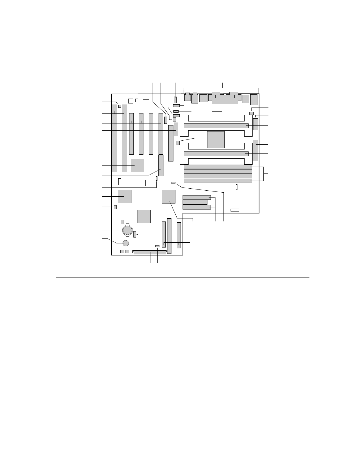
1.3 Motherboard Components
NN
MM
LL
KK
JJ
HH
GG
FF
EE
DD
CC
BB
B C
E
F
G
II
RS Q P
T
HA D
I
J
K
L
M
N
O
AA
W V UXYZ
OM06271
Figure 1. Motherboard Components
12
Page 13

Motherboard Description
A Serial port 2 header (optional) U Narrow (8-bit) SCSI connector
B Rear chassis fan header V Sleep LED header
C ATAPI CD audio connector (optional) W Front panel I/O header
D ATAPI-style telephony connector (optional) X AIC-7895 SCSI Host Adapter
E ATAPI-style Line In connector (optional) Y HDD LED input header (4-pin)
F 2 mm CD audio connector (optional) Z Front chassis 2 fan header
G CPU 2 fan header AA Front chassis 1 fan header
H Back panel I/O connectors BB Speaker
I CPU 1 fan header CC Battery
J Auxiliary power connector DD HDD LED header (2-pin)
K Boot processor Slot 1 EE Wake-on-Modem header
L Intel 82443LX PAC FF PC97307 SuperI/O Controller
M ATX power connector GG Wake on LAN header
port
N Application processor Slot 1 HH SCSI PCI RAID
O DIMM sockets II Intel 82557 PCI LAN Controller
P Configuration jumper block JJ A.G.P. connector
Q IDE connectors KK MIDI/Game Port connector (optional)
R Floppy drive connector LL PCI slots
S Intel 82371AB PIIX4 MM ISA slots
T Ultra-wide (16-bit) SCSI connectors NN Chassis security header
connector
13
Page 14
DK440LX Motherboard Technical Product Specification
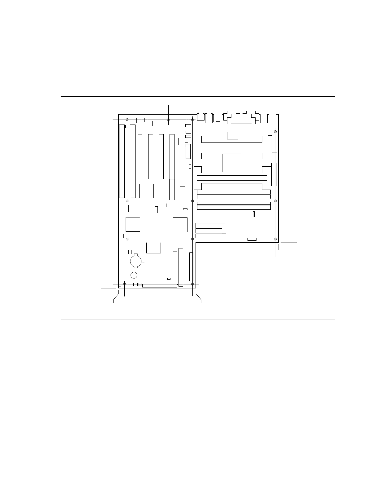
1.4 Custom Form Factor
The motherboard is designed to fit into an ATX form-factor chassis. Figure 2 shows that the I/O
connector locations and the mounting hole locations are in compliance with the ATX specification
(see Section 7.2).
0.20 3.30
12.70
12.30
11.40
0.30
0.00
0.00
5.10
5.350.45
Figure 2. Motherboard Dimensions
11.30
6.20
3.35
11.55
3.10
OM06273
14
Page 15
Motherboard Description
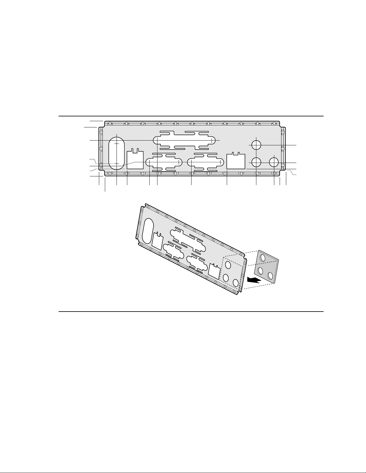
1.5 I/O Shield
The back panel I/O shield for the motherboard must meet specific dimension and material
requirements. Systems based on this motherboard need the back panel I/O shield to pass EMI
compliance verification. Figure 3 shows the critical dimensions of a chassis-independent I/O
shield and the location of the EMI gasket on the I/O shield. Additional design considerations for
I/O shields relative to chassis requirements are described in the ATX specification. See Section 7.2
for information about the ATX specification.
0.201
0.00
0.461
1.209
1.216
1.433
1.689
0.207
0.00
0.409
0.773
1.534
1.803
Outside(Rear)
View of Shield
2.959
4.180
5.184
EMI Gasket
5.785
5.975
0.617
1.207
1.450
1.489
6.183
OM06888
Figure 3. Back Panel I/O Shield Dimensions (ATX Chassis-Independent)
15
Page 16

DK440LX Motherboard Technical Product Specification
1.6 Processor
The motherboard supports configurations of one or two Pentium II processors. The processor’s
VID pins automatically program the voltage regulator on the motherboard to the required processor
voltage. The motherboard currently supports processors that run internally at 233 MHz, 266 MHz,
or 300 MHz , have a 512 KB second-level cache, and identical processor voltages. In order to
ensure reliable motherboard operation across the widest possible range of processor and chassis
combinations, it is recommended that only Pentium II processors with fan/heatsinks be installed on
the DK440LX motherboard.
1.6.1 Processor Packaging
The processor is packaged in a Single Edge Contact (S.E.C.) cartridge. The cartridge includes the
processor core, second-level cache, thermal plate, and back cover.
The processor connects to the motherboard through the Slot 1 connector, a 242-pin edge connector.
When mounted in a Slot 1 connector, the processor is secured by a retention mechanism attached to
the motherboard.
1.6.2 Second Level Cache
The second-level cache is located on the substrate of the S.E.C. cartridge. The ECC cache includes
burst pipelined synchronous static RAM (BSRAM) and tag RAM. There are four BSRAM
components totaling 512 KB in size. Only up to 512 MB of system memory is cacheable.
1.6.3 Processor Upgrades
NOTE
✏
In a uniprocessor configuration, the processor must be installed in the boot processor slot (the slot
closest to the back panel) and a termination card must be installed in the application processor
slot. If the processor is installed in the application processor slot, the computer will not boot.
Two microprocessor upgrades are available:
• Upgrade to a higher speed processor(s)
• Single to dual processors
If you are installing two processors, the following values must be identical for both processors:
• L2 cache size and type (ECC or non-ECC)
• Operating voltages
• Bus and core frequencies
The core stepping value may differ by one step, such as C0 to C1. These values can be determined
by checking the parameters of the s-spec number. The s-spec number is a five-character code, for
example, SL28R, printed on the top edge of the S.E.C.
For information about s-spec parameters, refer to the Pentium II processor quick reference guide at
the Intel developer’s web site.
16
Page 17

Motherboard Description
CAUTION
If the operating voltages do not match, the computer will not boot.
When upgrading the processor, use the BIOS configuration mode to change the processor speed if
necessary (see Section 1.18.2).
1.7 Memory
1.7.1 Main Memory
The motherboard has four dual inline memory module (DIMM) sockets. Minimum memory size is
16 MB; maximum memory size is 512 MB with SDRAM and 1 GB with EDO DRAM. The BIOS
automatically detects memory type, size, and speed.
The motherboard supports the following memory features:
• JEDEC MO-161 compliant 168-pin DIMMs with gold-plated contacts (see Section 7.2 for
information about this specification)
• Unbuffered 66-MHz ECC/non-ECC SDRAM or 60-ns EDO ECC/non-ECC DIMMs
• 3.3 V memory only
• Single- or double-sided DIMMs in the sizes listed in Table 1
Table 1. Supported DIMM Sizes
DIMM Size Configuration
16 MB 2 Mbit x 72/64
32 MB 4 Mbit x 72/64
64 MB 8 Mbit x 72/64
128 MB 16 Mbit x 72/64
256 MB (EDO DRAM only) 32 Mbit x 72/64
Memory can be installed in one, two, three, or four sockets. Memory type, size, and speed can
vary between sockets, so EDO and SDRAM DIMMs can be installed on the same motherboard.
NOTE
✏
There may be mechanical interference with the DIMM 0 socket (J6G3) and the DIMM 1 (J6G2)
socket in some combinations of ATX chassis and peripherals, such as CD-ROMs.
NOTE
✏
The DK440LX motherboard supports DIMMs with both asymmetrically and symmetrically
addressable DRAMs.
17
Page 18

DK440LX Motherboard Technical Product Specification
1.7.2 SDRAM
Synchronous DRAM (SDRAM) improves memory performance through memory access that is
synchronous with the memory clock. This simplifies the timing design and increases memory
speed because all timing is dependent on the number of memory clock cycles.
1.7.3 ECC Memory
Error checking and correcting (ECC) memory detects multiple-bit errors and corrects single-bit
errors. When ECC memory is installed, the BIOS supports both ECC and non-ECC mode. ECC
mode is enabled in the Setup program. The BIOS automatically detects if ECC memory is
installed and provides the Setup option for selecting ECC mode.
1.8 Chipset
The Intel 440LX AGPset is designed for the Pentium II processor and the Accelerated Graphics
Port (A.G.P.). It consists of the Intel 82443LX PCI/A.G.P. controller (PAC) and the Intel
82371AB PCI/ISA IDE Xccelerator (PIIX4) bridge chip.
1.8.1 Intel 82443LX PCI/A.G.P. Controller (PAC)
The PAC provides bus-control signals, address paths, and data paths for transfers between the
processor’s host bus, PCI bus, the A.G.P., and main memory. The PAC features:
• Processor interface control
Processor host bus speed at 66 MHz
Support for dual Pentium II processor configurations
32-bit addressing
GTL+ compliant host bus interface
• Integrated DRAM controller
Supports synchronous DRAM (SDRAM) and EDO
64/72-bit path-to-memory
Auto detection of memory type
Supports 4-, 16-, 64-Mbit DRAM devices
Symmetrical and asymmetrical DRAM addressing
Supports 3.3 V DRAMs
• Accelerated Graphics Port Interface
Complies with A.G.P. specification (see Section 7.2 for specification information)
Supports 3.3 V A.G.P. devices with data transfer rates up to 532 MB/sec
Synchronous coupling to the host-bus frequency
• Fully-synchronous PCI bus interface
Complies with PCI specification (see Section 7.2 for specification information)
PCI-to-DRAM access greater than 100 MB/sec
Supports five PCI bus masters in addition to the host and PCI-to-ISA I/O bridge
Delayed transactions
18
Page 19

Motherboard Description
• Data Buffering
Host-to-DRAM, PCI-to-DRAM, and A.G.P.-to-DRAM write-data buffering
Write-combining for host-to-PCI burst writes
Supports concurrent host, PCI, and A.G.P. transactions to main memory
• Supports system management mode (SMM)
1.8.2 Intel 82371AB PCI ISA IDE Xcelerator (PIIX4)
The PIIX4 is a multifunction PCI device implementing the PCI-to-ISA bridge, PCI IDE
functionality, Universal Serial Bus (USB) host/hub function, and enhanced power management.
The PIIX4 features:
• Multifunction PCI-to-ISA bridge
Supports the PCI bus at 33 MHz
Complies with PCI specification (see Section 7.2 for specification information)
Full ISA bus support
• USB controller
Two USB ports (see Section 7.2 for specification information)
Supports legacy keyboard and mouse
Supports UHCI Design Guide, revision 1.1, interface
• Integrated dual-channel enhanced IDE interface
Supports up to four IDE devices
PIO Mode 4 transfers at up to 14 MB/sec
Supports Ultra DMA/33 synchronous DMA mode transfers up to 33 MB/sec
Bus master mode with an 8 x 32-bit buffer for bus master PCI IDE burst transfers
• Enhanced DMA controller
Two 8237-based DMA controllers
Supports PCI DMA with three PC/PCI channels and distributed DMA protocols
Fast type-F DMA for reduced PCI bus usage
• Interrupt controller based on 82C59
Supports 15 interrupts
Programmable for edge/level sensitivity
• Power management logic
Sleep/resume logic
Supports Wake-on-Modem, Wake on LAN technology, and wake on PME
• Real-Time Clock
256 byte battery-backed CMOS SRAM
Includes date alarm
• 16-bit counters/timers based on 82C54
19
Page 20

DK440LX Motherboard Technical Product Specification
1.8.3 Intel 82093AA I/O Advanced Programmable Interrupt Controller (IOAPIC)
The Intel 82093AA I/O Advanced Programmable Interrupt Controller (IOAPIC) provides interrupt
management and incorporates both static and dynamic symmetric interrupt distribution across all
processors in a multiprocessor system. The 82093AA IOAPIC features 24 interrupts as follows:
• 13 ISA interrupts
• Four PCI interrupts
• One Interrupt/SMI# rerouting
• Two motherboard interrupts
• One interrupt used for INTR input
• Three general purpose interrupts
1.8.4 Accelerated Graphics Port (A.G.P.)
The Accelerated Graphics Port (A.G.P.) is a high-performance interconnect for graphic-intensive
applications, such as 3D applications. A.G.P. is independent of the PCI bus and is intended for
exclusive use with graphical display devices. A.G.P. provides these performance features:
• Pipelined-memory read and write operations that hide memory access latency
• Demultiplexing of address and data on the bus for near 100 percent bus efficiency
• AC timing for 133 MHz data transfer rates, allowing data throughput of 533 MB/sec
See Section 7.2 for more information about the A.G.P. specification.
1.8.5 Universal Serial Bus (USB)
The motherboard has two USB ports; one USB peripheral can be connected to each port. For more
than two USB devices, an external hub can be connected to either port. The motherboard fully
supports the universal host controller interface (UHCI) and uses UHCI-compatible software
drivers. See Section 7.2 for information about the USB specification. USB features include:
• Self-identifying, hot pluggable peripherals
• Automatic mapping of function to driver and configuration
• Support of isochronous and asynchronous transfer types
• Support for a maximum of 127 physical devices
• Guaranteed bandwidth and low latencies appropriate for telephony, audio, and other
applications
• Error handling and fault recovery mechanisms built into protocol
NOTE
✏
Computer systems that have an unshielded cable attached to a USB port may not meet FCC
Class B requirements, even if no device or a low-speed USB device is attached to the cable. Use
shielded cable that meets the requirements for high-speed devices.
20
Page 21

Motherboard Description
1.8.6 IDE Support
The motherboard has two independent bus-mastering IDE interfaces. These interfaces support PIO
Mode 3, PIO Mode 4, ATAPI devices (e.g., CD-ROM), and Ultra DMA synchronous-DMA mode
transfers. The BIOS supports logical block addressing (LBA) and extended cylinder head sector
(ECHS) translation modes. The BIOS automatically detects the IDE device transfer rate and
translation mode.
The motherboard supports LS-120 diskette technology through its IDE interfaces. LS-120 diskette
technology enables users to store 120 MB of data on a single, 3.5-inch removable diskette. LS-120
technology is backward (both read and write) compatible with 1.44 MB and 720 KB DOS-
†
formatted diskettes and is supported by Windows
95 and Windows NT† operating systems.
The motherboard allows connection of an LS-120 compatible drive and a standard 3.5-inch diskette
drive. If an LS-120 drive is connected to an IDE connector and configured as the A drive and a
standard 3.5-inch floppy is configured as a B drive, the standard floppy must be connected to the
floppy drive cable's "A" connector (the connector at the end of the cable). The LS-120 drive can be
configured as a boot device, if selected in the BIOS setup utility.
1.8.7 Real-Time Clock, CMOS SRAM, and Battery
The real-time clock is compatible with DS1287 and MC146818 components. The clock provides a
time-of-day clock and a multicentury calendar with alarm features and century rollover. The realtime clock supports 256 bytes of battery-backed CMOS SRAM in two banks that are reserved for
BIOS use.
The time, date, and CMOS values can be specified in the Setup program. The CMOS values can
be returned to their defaults by using the Setup program.
An external coin-cell battery powers the real-time clock and CMOS memory. When the computer
is not plugged into a wall socket, the battery has an estimated life of three years. When the
computer is plugged in, the 3 V standby current from the power supply extends the life of the
battery. The clock is accurate to ± 13 minutes/year at 25 ºC with 5 V applied.
21
Page 22

DK440LX Motherboard Technical Product Specification
1.9 SuperI/O Controller
The PC97307 SuperI/O controller from National Semiconductor is an ISA Plug and Play
compatible (see Section 7.2), multifunction I/O device that provides the following features:
• Serial ports
Two 16450/16550A-software compatible UARTs
Internal send/receive 16-byte FIFO buffer
Four internal 8-bit DMA options for the UART with SIR support (USI)
• Multimode bidirectional parallel port
Standard mode: IBM and Centronics compatible
Enhanced parallel port (EPP) mode with BIOS and driver support
High-speed extended capabilities port (ECP) mode
• Floppy disk controller
DP8473 and N82077 compatible
16-byte FIFO buffer
†
PS/2
High-performance digital data separator (DDS)
PC-AT
• Keyboard and mouse controller
Industry standard 8042A compatible
General-purpose microcontroller
8-bit internal data bus
diagnostic-register support
†
, PS/2, and 3-mode floppy disk drive-mode support
By default, the I/O controller interfaces are automatically configured during boot up. The I/O
controller can also be manually configured in the Setup program.
1.9.1 Serial Ports
The two 9-pin D-Sub serial port connectors on the back panel are compatible with 16450 and
16550A UARTs. An optional onboard keyed 10-pin header is available for internal cabling of
serial port 2. If the optional onboard serial port 2 header is installed, the 9-pin D-Sub serial port 2
connector is not installed.
1.9.2 Parallel Port
The connector for the multimode bidirectional parallel port is a 25-pin D-Sub connector located on
the back panel. In the Setup program, the parallel port can be configured for the following:
• Compatible (standard mode)
• Bidirectional (PS/2 compatible)
• Extended Parallel Port (EPP)
• Enhanced Capabilities Port (ECP)
22
Page 23

Motherboard Description
1.9.3 Floppy Controller
The I/O controller is software compatible with the DP8473 and N82077 floppy drive controllers
and supports both PC-AT and PS/2 modes. In the Setup program, the floppy interface can be
configured for the following floppy drive capacities and sizes:
• 360 KB, 5.25-inch
• 1.2 MB, 5.25-inch
• 720 KB, 3.5-inch
• 1.2 MB, 3.5-inch (driver required)
• 1.25/1.44 MB, 3.5-inch
• 2.88 MB, 3.5-inch
1.9.4 Keyboard and Mouse Interface
PS/2 keyboard and mouse connectors are located on the back panel. The 5 V lines to these
connectors are protected with a PolySwitch
connection after an over-current condition is removed.
NOTE
✏
The mouse and keyboard can be plugged into either of the PS/2 connectors. Power to the
computer should be turned off before a keyboard or mouse is connected or disconnected.
The keyboard controller contains the AMI Megakey keyboard and mouse controller code, provides
the keyboard and mouse control functions, and supports password protection for power on/reset. A
power on/reset password can be specified in Setup.
The keyboard controller also supports the hot-key sequence <Ctrl><Alt><Del> for a software
reset. This key sequence resets the computer’s software by jumping to the beginning of the BIOS
code and running the Power-On Self Test (POST).
†
circuit that, like a self-healing fuse, reestablishes the
23
Page 24

DK440LX Motherboard Technical Product Specification
1.10 Audio Subsystem
The optional onboard audio subsystem features the Crystal CS4236B, an audio codec with an
integrated FM synthesizer. The audio subsystem provides all the digital audio and analog mixing
functions needed for recording and playing sound on personal computers. Together, these
components feature the following:
• Stereo analog-to-digital and digital-to-analog converters
• Analog mixing, anti-aliasing, and reconstruction filters
• Line and microphone level inputs
• ADPCM, A-law, or µlaw digital audio compression/decompression
• Full digital control of all mixer and volume control functions
• High-quality, 16-bit, MPC-II compliant onboard audio
• Full duplex operation
• AdLib, Sound Blaster Pro 2.0, Windows Sound System, and MPU-401 support
• Full DOS games compatibility
• MIDI/Game port support
• OPL3 compatible FM synthesizer
• BIOS Setup-based enable/disable
• Onboard Crystal CS9236 Wavetable Music Synthesizer (optional)
The audio subsystem requires up to two DMA channels and one IRQ. Table 2 shows the IRQ,
DMA channel, and base I/O address options. These options are automatically chosen by the Plug
and Play interface, so there are no default settings.
Table 2. Audio Subsystem Resources
IRQ
Resource
Sound Blaster
(DMA playback, DMA / IRQ shared
with Windows Sound System capture)
Windows Sound System
(DMA playback)
MPU-401
(IRQ shared with Sound Blaster)
MIDI 200-207h
FM Synthesis 388-38Dh
†
(Options)
5 (best choice)
7
10 (best choice)
11
5
7
10 (best choice)
11
5 (best choice)
7
10 (best choice)
11
DMA Channel
(Options)
0 (best choice)3210-21Fh
0
1 (best choice)
3
I/O Address
(Options)
220-22Fh (best choice)
230-234h
240-24Fh
250-25Fh
260-26Fh
534-537h (best choice)
608-60Bh
300-301h
330-331h (best choice)
332-333h
334-335h
24
CS4236B Control FF0-FFFh
Page 25

1.10.1 Audio Subsystem Performance
Table 3 lists the performance characteristics of the audio subsystem.
Table 3. Audio Subsystem Performance
Characteristic Test Result
Frequency Response -1.3 dB @ 20 Hz
-0.6 dB @ 20 kHz
Signal-to-Noise Ratio -91.05 dB
Total Harmonic Distortion vs. Amplitude 0.0044% @ -4.813 dB
Total Harmonic Distortion vs. Frequency 0.0042% @ 9355 Hz
Crosstalk L-to-R -92.69 dB
Crosstalk R-to-L -93.12 dB
1.10.2 Audio Drivers and Utilities
Motherboard Description
Audio software and utilities are available from Intel’s World Wide Web site (see Section 7.1).
Audio driver support is provided for the Microsoft Windows NT
†
Windows 95, and IBM OS/2
Warp† (versions 3.0 and 4.0) operating systems.
(versions 3.51 and 4.0), Microsoft
1.10.3 Audio Connectors
The audio connectors include the following:
• Back panel connectors: Line In, Line Out, Mic In (see Section 1.16.4)
• CD-ROM audio (ATAPI or 2 mm)
• Telephony (ATAPI style)
• MIDI/Game port header
• Line In (ATAPI style)
See Section 1.16.4 for the location and pinouts of the audio connectors.
1.10.3.1 CD-ROM Audio
An optional 1 x 4-pin ATAPI-style (J1F1) or 1 x 4-pin 2 mm (J1E1) connector is available for
connecting an internal CD-ROM drive to the audio mixer.
1.10.3.2 Telephony
An optional 1 x 4-pin ATAPI-style connector (J0E1) is available for connecting the monaural
audio signals of an internal telephony device, such as a modem, to the audio subsystem. A
monaural audio-in and audio-out signal interface is necessary for telephony applications such as
speakerphones, modem, and answering machines.
1.10.3.3 MIDI/Game Port Header
An optional 2 x 8-pin MIDI/Game port header (J2E2) is available for connecting MIDI devices and
joysticks.
25
Page 26

DK440LX Motherboard Technical Product Specification
1.10.3.4 Line In
An optional 1 x 4-pin ATAPI-style Line In connector (J0F2) is available for connecting the left and
right channel signals of an internal audio device to the audio subsystem. An audio-in signal
interface of this type is useful in applications such as TV tuners.
1.10.4 Hardware Wavetable Support
The optional hardware wavetable support is implemented with a Crystal CS9236 Wavetable Music
Synthesizer. The CS9236 device is a complete General MIDI wavetable music synthesizer on a
single chip. The MIDI interpreter, synthesis engine, effects processing, and all RAM and ROM
(including the wavetable sample ROM) are included on-chip. The CS9236 includes the following
features:
• General MIDI compliant
• 32-note polyphony at 44.1 kHz rate
• Independent reverb and chorus levels for each MIDI channel
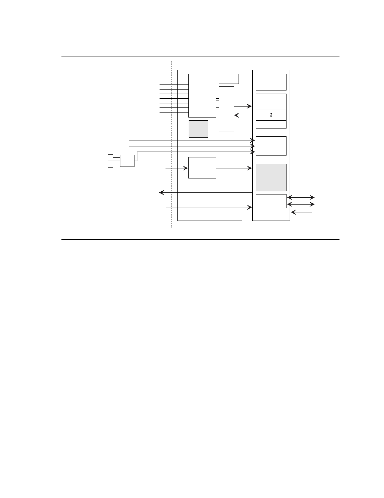
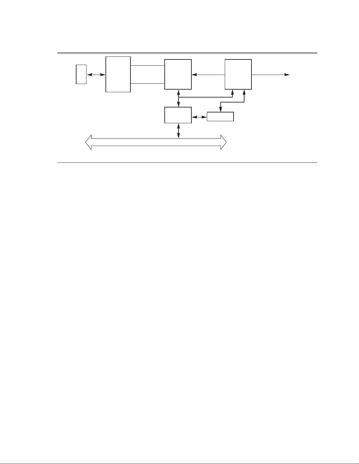
1.11 Hardware Monitor Subsystem
The hardware monitor subsystem includes a National Semiconductor LM79 Microprocessor
System Hardware Monitor, an analog multiplexer, and a chassis security header. Its features
include:
• Management Level 3 functionality.
• Integrated temperature and voltage sense monitoring to detect levels above or below acceptable
values (+12 V, -12 V, +5 V, -5 V, and +3.3V). When suggested ratings for temperature, fan
speed, or voltage are exceeded, an interrupt is activated.
• Fan speed sensors for up to five fans with the onboard analog multiplexer.
• Header for an external chassis security feature.
• 8-bit I/O map to ISA bus or access from SMBus.
Figure 4 shows a block diagram of the hardware monitor subsystem.
26
Page 27
LM79
Motherboard Description
Rear Chassis Fan
Front Chassis 1 Fan
Front Chassis 2 Fan
Control 3(8)
Status 4(8)
Limit 1(8)
Limit 2 (8)
Limit 17(8)
FAN Intvl
Timers (3)
POST Regs
(32 x 8)
Port 80/84
Shadow
2
I C I/F
Slave
CPU 1 Fan
CPU 2 Fan
Multi-
plexer
2 Pulse/Rev
2 Pulse/Rev
2 Pulse/Rev
Chassis
Security
Header
Power Switch
(Bypass)
BTI
VOLTAGE
+5 Sense
-5
+12
-12
+3.3
+2.5A
+2.5B
Temp
Sensor
Security
RESET
8 Bit
8 Ch
MUX
A/D
Figure 4. Block Diagram of Hardware Management Subsystem
SDA
SCL
VID[0...3]
OM06922
The 1 x 2-pin chassis security header (J0A1) can be connected to a normally-open mechanical
switch on the chassis. See Section 1.16 for the location and pinouts of the chassis security header.
1.12 EtherExpress PRO/100WfM PCI LAN Subsystem
The optional Intel EtherExpress PRO/100WfM PCI LAN subsystem (see Figure 5) is an
Ethernet
include:
•
•
•
•
•
†
LAN interface that provides both 10Base-T and 100Base-TX connectivity. Features
32-bit direct bus mastering on the PCI bus
Shared memory structure in the host memory that copies data directly to/from host memory
10Base-T and 100Base-TX capability using a single RJ-45 connector with connection and
activity status LEDs
IEEE 802.3µ Auto-Negotiation for the fastest available connection
Jumperless configuration; the LAN subsystem is completely software configurable
27
Page 28
DK440LX Motherboard Technical Product Specification
RJ-45
Common
Magnetic
Module
Connector
10 Mbit/sec
Xmit/Rcv
100 Mbit/sec
Xmit/Rcv
PCI Local Bus
Intel
82555
PHY
Intel
82557
PHY_RST# MP_WAKEUP
MII
EEPROM
Wake on
LAN
ASIC
Figure 5. LAN Subsystem Block Diagram
1.12.1 Intel 82557 LAN Controller
The Intel 82557 LAN Controller provides the following functions:
• CSMA/CD Protocol Engine
• PCI compatibility
• DMA engine for movement of commands, status, and network data across the PCI bus
• Standard MII interface for access to IEEE 802.3µ-compliant physical layer devices
(PIIX4)
OM06270A
1.12.2 10 / 100 Mbit/sec Physical Layer Interface
The physical layer interface is implemented by the Intel 82555 Physical Layer Interface (PHY)
device. This device provides:
• Complete functionality necessary for the 10Base-T and 100Base-TX interfaces; when in
10 Mbit/sec mode, the interface drives the cable directly
• A complete set of MII management registers for control and status reporting
• 802.3µ Auto-Negotiation for automatically establishing the best operating mode when
connected to other 10Base-T or 100Base-TX devices
1.12.3 Wake on LAN ASIC
The Wake on LAN ASIC performs remote wakeup of the motherboard via the onboard LAN
interface. When the system is powered off, the Wake on LAN ASIC remains powered by the 5 V
standby voltage. The ASIC monitors network traffic at the MII interface and when it detects a
Magic Packet
†
it asserts a wakeup signal that powers up the computer.
28
Page 29

Motherboard Description
1.12.4 LAN Subsystem Software
The EtherExpress PRO/100WfM PCI LAN software provided includes setup/diagnostic software
(SETUP.EXE), a readme file viewer (README.EXE) and the drivers listed in Table 4. The LAN
software is available from Intel’s World Wide Web site (see Section 7.1).
Table 4. EtherExpress PRO/100WfM PCI Drivers
Driver Description Environment(s)
E100BODI.COM Novell† ODI NetWare† DOS Client
E100BODI.SYS Novell ODI NetWare OS/2 Client
E100B.LAN Novell ODI NetWare 3.11 Server
NetWare 3.12 Server
NetWare 4.0x Server
NetWare NT Requester
NetWare for OS/2
E100B.DOS NDIS 2.0.1 Windows for Workgroups 3.11
MS-DOS
E100B.OS2 NDIS 2.0.1 MS OS/2 1.3
IBM OS/2 2.11
IBM OS/2 Warp
E100B.SYS NDIS 3.X Windows 95
Windows NT 3.5x
E100BNT.SYS NDIS 4.0 Windows NT 4.0
†
LANMAN 2.1
1.13 Wake on LAN Header
Header J6D1 is used to implement the Wake on LAN feature. Connect this header to a network
interface card (NIC) that supports the Wake on LAN technology. The NIC monitors network
traffic. When the NIC detects a Magic Packet, it asserts a signal through the Wake on LAN header
to wake up the computer. This signal can wake up the computer only when the power cord is still
plugged into the socket and the computer is turned off. Wake on LAN can be enabled through the
BIOS Setup program.
NOTE
✏
The computer’s power supply must provide sufficient +5 VSB current to the NIC; without enough
+5 VSB current, the Wake on LAN feature will not function and the motherboard may not boot.
Check the NIC’s documentation for its +5 VSB current requirements. See Section 1.22 for
information on the motherboard’s power requirements.
1.14 Wake on Modem
The Wake-on-Modem feature allows the computer to wake from Sleep mode when a call is
received on a telephony device, such as a modem. The first incoming call will power up the
motherboard, but a second call must be made to access the computer.
29
Page 30

DK440LX Motherboard Technical Product Specification
1.15 SCSI Subsystem
The onboard SCSI subsystem features the Adaptec AIC-7895, which contains a dual-channel SCSI
controller and a PCI bus master interface. The AIC-7895 supports the following:
• Narrow (8-bit, 50-pin) or Wide (16-bit, 68-pin) Fast SCSI providing 10-20 MB/sec throughput
per channel
• Narrow (8-bit, 50-pin) or Wide (16-bit, 68-pin) Ultra SCSI providing 20-40 MB/sec
throughput per channel
• Burst data transfers on the PCI bus up to the maximum rate of 133 MB/sec per channel using
the on-chip 256-byte FIFO buffer
• RAIDport connector interface
• Two Wide 68-pin connectors
• One Narrow 50-pin connector
• Subsystem Vendor and Device ID support
• Spin down of SCSI drive
• SCAM (SCSI Configured Automatically) Level 2
1.15.1 SCSI Drivers and Utilities
SCSI drivers are available from Intel’s World Wide Web site (see Section 7.1). SCSI driver
support is provided for the Microsoft Windows NT
Windows 95, and IBM OS/2 Warp (versions 3.0 and 4.0) operating systems.
(versions 3.51 and 4.0), Microsoft
1.15.2 SCSI Interface
The AIC 7895 also offers active negation outputs and a disk activity output signal. Active
negation outputs reduce the chance of data errors by actively driving both polarities of the SCSI
bus, avoiding indeterminate voltage levels. The SCSI output drivers can directly drive a 48 mA
single-ended SCSI bus with no additional drivers. Synchronous SCSI can handle up to 15 REQ
control signals simultaneously.
1.15.3 SCSI Bus
Each channel’s SCSI data bus is 8- or 16-bits wide with odd ECC generated per byte. SCSI
control signals are the same for either bus width. The motherboard has three onboard SCSI
connectors. Channel A has a high-density 68-pin Wide connector, while channel B has a highdensity 68-pin Wide connector as well as a 50-pin Narrow connector (see Figure 7). On a 16-bit
wide SCSI bus, the AIC-7895 assigns the highest arbitration priority to the low byte of the 16-bit
word. This way, 16-bit targets can be mixed with 8-bit targets if the 8-bit devices are placed on the
low data byte. During chip powerdown, all inputs are disabled to reduce power consumption.
30
Page 31
Motherboard Description
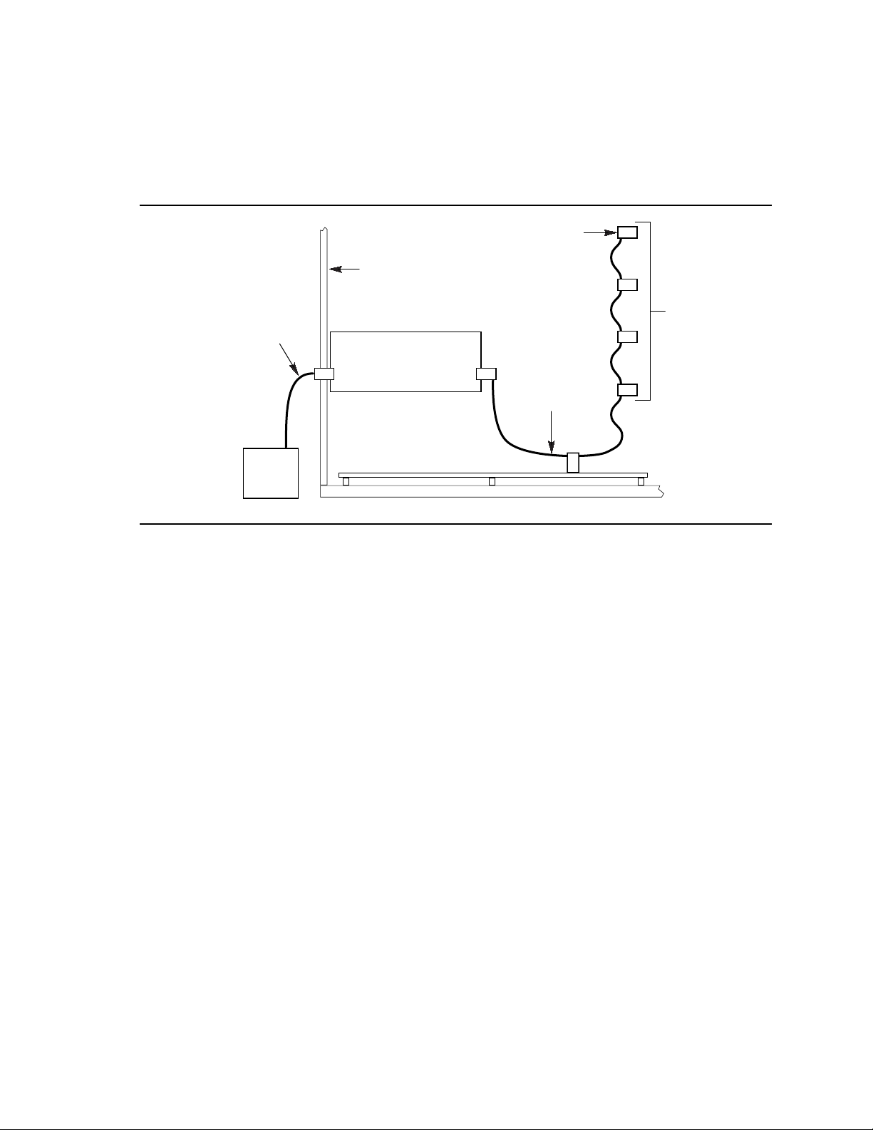
1.15.3.1 SCSI Bus Topology
Figure 6 shows a typical single-channel SCSI bus implementation with internal and external
devices.
Last
Internal
Device
Chassis
Single-or Dual-
Connector
External SCSI
Cable
External
SCSI
Device
Single-or Dual-Connector
Terminator Card
Motherboard
Internal
SCSI
Cable(s)
Internal
SCSI
Devices
OM06274A
Figure 6. Single-channel SCSI Bus Topology
From end to end, a SCSI cable is routed, in a daisy chain fashion, from the last internal SCSI
device to each subsequent internal device including the onboard host controller. The cable can
then continue to an optional terminator card installed in an unused I/O slot of the chassis. From
the terminator card, an optional external SCSI cable can be used to connect external SCSI devices.
1.15.3.2 SCSI Cable
For proper operation of ultra/wide SCSI devices, the overall length of the SCSI cable from the last
internal device to the last external device should not exceed 3 meters with four Ultra Wide SCSI
peripherals and 1.5 meters with eight peripherals per channel (within constraints defined by the
ANSI SCSI-3 Specification).
31
Page 32

DK440LX Motherboard Technical Product Specification
1.15.3.3 Channel A SCSI Bus Termination
Terminate the extreme ends of the SCSI bus (cable), typically by connecting a terminated device to
the end connectors of the cable:
• On the last connector of the internal cable (farthest from the motherboard), attach either a
terminated 16-bit device or some other type of 16-bit termination.
• If the internal cable ends at the motherboard, enable motherboard termination in the SCSI
BIOS (on bootup press <Ctrl><A> to enter the SCSISelect
• If the internal cable does not end at the motherboard, but continues on to the external
termination card, disable motherboard termination in the SCSI BIOS (using SCSISelect).
• If an external SCSI cable is attached to the terminator card, the terminator card’s termination is
disabled automatically. On the last connector of the external cable, attach either a terminated
16-bit device or some other type of 16-bit termination.
When using 16-bit SCSI devices on channel A:
• Use the onboard 68-pin Wide connector for cabling to 16-bit devices.
• Enable termination only on the last device on the SCSI cable (internal and/or external).
• Remove or disable termination on all other devices.
†
utility).
1.15.3.4 Channel B SCSI Bus Termination
Terminate the extreme ends of the SCSI bus (cable), typically by connecting a terminated device to
the end connectors of the cable:
• On the last connector of the internal cable (farthest from the motherboard), attach either a
terminated 16-bit device or some other type of 16-bit termination.
• If the internal cable ends at the motherboard, enable motherboard termination in the SCSI
BIOS (on bootup press <Ctrl><A> to enter the SCSISelect
• If the internal cable does not end at the motherboard, but continues on to the external
termination card, disable motherboard termination in the SCSI BIOS (using SCSISelect).
• If an external SCSI cable is attached to the terminator card, the termination card’s termination
is disabled automatically. On the last connector of the external cable, attach either a terminated
16-bit device or some other type of 16-bit termination.
When using 16-bit SCSI devices on channel B:
• Use the onboard 68-pin Wide connector for cabling to 16-bit devices.
• Enable termination only on the last device on the SCSI cable (internal and/or external).
• Remove or disable termination on all other devices.
When using 8-bit SCSI devices on channel B:
• Use the onboard 50-pin connector for cabling to 8-bit devices.
• If the cable does not end at the motherboard, but continues to external devices, disable onboard
SCSI termination through the SCSISelect utility and the Channel B termination option in BIOS
setup.
utility).
32
Page 33

Motherboard Description
1.15.4 SCSI
See Chapter 5.
Select
1.15.5 Adaptec RAID
The onboard RAIDport connector, in conjunction with an ARO†-1130CA-B Adaptec RAIDport
card and the SCSI controller, provides a complete client RAID solution. The RAIDport card
supports the following features for enhancing performance, data redundancy, and data availability:
• RAID coprocessor
• Support for RAID levels 0 (data striping), 1 (mirroring), and 0/1
• Hot-swap drive support
• Hot-spare standby
• Dynamic sector repairing
For information on obtaining a RAIDport card, visit Adaptec’s web page at
http://www.adaptec.com.
and SCSI Disk Utilities
port
33
Page 34

DK440LX Motherboard Technical Product Specification
1.16 Motherboard Connectors
The following figure shows the location of the motherboard connectors.
Chassis
Security
J2E3
B1
B66
A.G.P.
Front Chassis 1
J12A1
1
Serial
Port 2
9
J0A1
J1E2
1
J2E2
12
MIDI/
A1
Game
Port
B01
A01
Modem
B30
RAID
A30
port
J4D1
J12D1
A66
Sleep LED
Fan
1
J12E1
Front Panel I/O
Rear
Chassis
2
10
Fan
1
J2E1
ISA
Slots(2)
1615
PCI
Slots(4)
Wake-
1
on-
J9A1
HDD
LED
1
J10A1
1
Front Chassis 2
Fan
1
J12B2
J1E1
1
CD Audio
J1F1
ATAPI CD
Audio
J11B1
HDD
LED
Narrow
SCSI
Channel B
J10E1
1
J0F2
Line-In
1
B
A
12
1
49 50
1
Boot
Processor
Application
Processor
Slot 1
135
6834
Wide Ultra
SCSI
Channel
A & B
J10F1
J10D1
J0E1
1
Telephony
CPU 1
Auxiliary
Power
J1M2
1
Fan
1
Slot 1
J1M1
CPU 2
Fan
1
J3F2
J5M1
10
20
DIMM Sockets(4)
Bank 3 J5G1
Bank 2 J6G1
Bank 1 J6G2
Bank 0 J6G3
1
Wake
1
11
Power
on LAN
J6D1
IDE(2)
139
J8F1-Secondary
40202
J9F1-Primary
J8F2
234
1
Floppy
335
OM06921
34
Figure 7. Motherboard Connectors
Page 35

Table 5. Chassis Security Header (J0A1)
Pin Signal Name
1 Ground
2 TAMPER_DETECT#
Table 6. ATAPI CD Audio Connector (J1F1)
Pin Signal Name
1 Left CD In
2 CD_common
3 CD_common
4 Right CD In
Table 7. ATAPI-Style Telephony Connector
(J0E1)
Pin Signal Name
1 MONO_IN (from external device)
2 Ground
3 Ground
4 TEL_MICIN
Motherboard Description
Table 8. ATAPI-Style Line In Connector
(J0F2)
Pin Signal Name
1 Left Line In
2 Ground
3 Ground
4 Right Line In (monaural)
Table 9. 2 mm CD Audio Header (J1E1)
Pin Signal Name
1 Right CD In
2 CD_common
3 Left CD In
4 CD_common
35
Page 36

DK440LX Motherboard Technical Product Specification
Table 10. MIDI/Game Port Header (J2E2)
Pin Signal Name
1 +5 V (fused)
2 +5 V (fused)
3 JAB1
4 JABB1
5 JACX
6 JBCX
7 Ground
8 MIDI-OUT
9 Ground
10 JBCY
11 JACY
12 JBB2
13 JAB2
14 MIDI-IN
15 +5 V (fused)
16 MIDI-PRESENT GP
Table 11. Front Chassis 2 Fan Header
(J12B2)
Pin Signal Name
1 FAN_SEN
2 +12 V
3 Ground
Table 12. CPU 2 Fan Header (J3F2)
Pin Signal Name
1 FAN_SEN
2 +12 V
3 Ground
Table 13. CPU 1 Fan Header (J1M1)
Pin Signal Name
1 FAN_SEN
2 +12 V
3 Ground
36
Page 37

Table 14. Rear Chassis Fan Header (J2E1)
Pin Signal Name
1 FAN_SEN
2 +12 V
3 Ground
Table 15. Front Chassis 1 Fan Header
(J12A1)
Pin Signal Name
1 FAN_SEN
2 +12 V
3 Ground
Table 16. Hard Drive LED Input Header
(J10A1)
Pin Signal Name
1 Ground
2 DRV_ACT#
Motherboard Description
Table 17. Hard Drive LED Input Header
(J11B1)
Pin Signal Name
1 Ground
2 DRV_ACT#
3 DRV_ACT#
4 Ground
Table 18. Wake on LAN Header (J6D1)
Pin Signal Name
1 +5 VSB
2 Ground
3 MP_WAKEUP
Table 19. Wake-on-Modem Header (J9A1)
Pin Signal Name
1 SLOT_RI_N
2 Ground
37
Page 38

DK440LX Motherboard Technical Product Specification
Table 20. Floppy Drive Connector (J8F2)
Pin Signal Name Pin Signal Name
1 Ground 2 DENSEL
3 Ground 4 Reserved
5 Key 6 FDEDIN
7 Ground 8 FDINDX# (Index)
9 Ground 10 FDM00# (Motor Enable A)
11 Ground 12 FDDS1# (Drive Select B)
13 Ground 14 FDDS0# (Drive Select A)
15 Ground 16 FDM01# (Motor Enable B)
17 MSEN1 18 FDDIR# (Stepper Motor Direction)
19 Ground 20 FDSTEP# (Step Pulse)
21 Ground 22 FDWD# (Write Data)
23 Ground 24 FDWE# (Write Enable)
25 Ground 26 FDTRK0# (Track 0)
27 MSEN0 28 FDWPD# (Write Protect)
29 Ground 30 FDRDATA# (Read Data)
31 Ground 32 FDHEAD# (Side 1 Select)
33 Ground 34 DSKCHG# (Diskette Change)
Table 21. PCI IDE Connectors (J9F1, J8F1)
Pin Signal Name Pin Signal Name
1 Reset IDE 2 Ground
3 Data 7 4 Data 8
5 Data 6 6 Data 9
7 Data 5 8 Data 10
9 Data 4 10 Data 11
11 Data 3 12 Data 12
13 Data 2 14 Data 13
15 Data 1 16 Data 14
17 Data 0 18 Data 15
19 Ground 20 Key
21 DDRQ0 [DDRQ1] 22 Ground
23 I/O Write# 24 Ground
25 I/O Read# 26 Ground
27 IOCHRDY 28 P_ALE (Cable Select pullup)
29 DDACK0# [DDACK1#] 30 Ground
31 IRQ 14 [IRQ 15] 32 Reserved
33 Address 1 34 Reserved
35 Address 0 36 Address 2
37 Chip Select 1P# [Chip Select 1S#] 38 Chip Select 3P# [Chip Select 3S#]
39 Activity# 40 Ground
NOTE: Signal names in brackets ([ ]) are for the secondary IDE connector.
38
Page 39

Motherboard Description
Table 22. Wide (16-bit) Ultra SCSI Connectors (J10F1, J10D1)
Pin Signal Name Pin Signal Name Pin Signal Name Pin Signal Name
1 GND 18 TERM_PWR 35 SCSI_D12 52 TERM_PWR
2 GND 19 N/C 36 SCSI_D13 53 N/C
3 GND 20 GND 37 SCSI_D14 54 GND
4 GND 21 GND 38 SCSI_D15 55 SCSI_ATN#
5 GND 22 GND 39 SCSI_DPH# 56 GND
6 GND 23 GND 40 SCSI_D0 57 SCSI_BSY#
7 GND 24 GND 41 SCSI_D1 58 SCSI_ACK#
8 GND 25 GND 42 SCSI_D2 59 SCSI_RST#
9 GND 26 GND 43 SCSI_D3 60 SCSI_MSG#
10 GND 27 GND 44 SCSI_D4 61 SCSI_SEL#
11 GND 28 GND 45 SCSI_D5 62 SCSI_CD#
12 GND 29 GND 46 SCSI_D6 63 SCSI_REQ
13 GND 30 GND 47 SCSI_D7 64 SCSI_IO#
14 GND 31 GND 48 SCSI_DPL# 65 SCSI_D8
15 GND 32 GND 49 GND 66 SCSI_D9
16 GND 33 GND 50 GND 67 SCSI_D10
17 TERM_PWR 34 GND 51 TERM_PWR 68 SCSI_D11
Table 23. Narrow (8-bit) SCSI Connector (J10E1)
Pin Signal Name Pin Signal Name Pin Signal Name Pin Signal Name
1 Ground 14 Data6 27 No connect 40 RST
2 DATA0 15 Ground 28 No connect 41 Ground
3 Ground 16 Data7 29 Ground 42 MSG
4 DATA1 17 Ground 30 Ground 43 Ground
5 Ground 18 Data8 31 Ground 44 SEL
6 DATA2 19 Ground 32 ATTN 45 Ground
7 Ground 20 Ground 33 Ground 46 -CD
8 DATA3 21 Ground 34 Ground 47 Ground
9 Ground 22 Ground 35 Ground 48 REQ
10 Data4 23 No connect 36 BSY 49 Ground
11 Ground 24 No connect 37 Ground 50 IO
12 Data5 25 No connect 38 ACK
13 Ground 26 No connect 39 Ground
39
Page 40

DK440LX Motherboard Technical Product Specification
Table 24. RAID
Pin Signal Name Pin Signal Name Pin Signal Name Pin Signal Name
B01 No connect B16 MD[0] A01 No connect A16 MDP
B02 No connect B17 MD[2] A02 No connect A17 MD[1]
B03 Ground B18 MD[4] A03 No connect A18 RAMPS#
B04 No connect B19 Ground A04 No connect A19 MD[3]
B05 REQ[A]# B20 MD[6] A05 ACK[A]# A20 MD[5]
B06 RSVD B21 MA[14] A06 RSVD A21 MA[13]
B07 REQ[B]# B22 MA[12] A07 ACK[B]# A22 MD[7]
B08 REQ[C]# B23 MA[10] A08 ACK[C]# A23 MA[11]
B09 LED[A]# B24 MA[8] A09 IDDAT A24 MA[9]
B10 No connect B25 PRSNT1 A10 No connect A25 MA[7]
B11 No connect B26 MA[6] A11 No connect A26 Ground
B12 RSVD B27 MA[4] A12 SY_RST# A27 MA[5]
B13 CLK40 B28 Ground A13 ROMCS[A]# A28 MA[3]
B14 Ground B29 MA[2] A14 RAMCS# A29 SEECS[A]
B15 MRW B30 MA[0] A15 Ground A30 MA[1]
port
Connector (J4D1)
40
Page 41

Motherboard Description
Table 25. A.G.P. Connector (J2E3)
Pin Signal Name Pin Signal Name Pin Signal Name Pin Signal Name
A1 +12V B1 No Connect A34 Vcc3.3 B34 Vcc3.3
A2 No Connect B2 Vcc A35 AGP_AD22 B35 AGP_AD21
A3 Reserved B3 Vcc A36 AGP_AD20 B36 AGP_AD19
A4 No Connect B4 No Connect A37 Ground B37 Ground
A5 Ground B5 Ground A38 AGP_AD18 B38 AGP_AD17
A6 PIRQ0# B6 PIRQ1# A39 AGP_AD16 B39 AGP_CBE2#
A7 RST# B7 HCLK_AGP A40 Vcc3.3 B40 Vcc3.3
A8 AGP_GNT1# B8 AGP_REQ1 A41 AGP_FRAME# B41 AGP_IRDY#
A9 Vcc3.3 B9 Vcc3.3 A42 Reserved B42 Reserved
A10 AGP_ST1 B10 AGP_ST0 A43 Ground B43 Ground
A11 Reserved B11 AGP_ST2 A44 Reserved B44 Reserved
A12 AGP_PIPE# B12 AGP_RBF# A45 Vcc3.3 B45 Vcc3.3
A13 Ground B13 Ground A46 AGP_TRDY# B46 AGP_DEVSEL#
A14 No Connect B14 No Connect A47 AGP_STOP# B47 Vcc3.3
A15 SBA1 B15 SBA0 A48 No Connect B48 AGP_PERR#
A16 Vcc3.3 B16 Vcc3.3 A49 Ground B49 Ground
A17 SBA3 B17 SBA2 A50 AGP_PAR B50 AGP_SERR#
A18 Reserved B18 SB_STB A51 AGP_AD15 B51 AGP_CBE1#
A19 Ground B19 Ground A52 Vcc3.3 B52 Vcc3.3
A20 SBA5 B20 SBA4 A53 AGP_AD13 B53 AGP_AD14
A21 SBA7 B21 SBA6 A54 AGP_AD11 B54 AGP_AD12
A22 Key B22 Key A55 Ground B55 Ground
A23 Key B23 Key A56 AGP_AD9 B56 AGP_AD10
A24 Key B24 Key A57 AGP_CBE0# B57 AGP_AD8
A25 Key B25 Key A58 Vcc3.3 B58 Vcc3.3
A26 AGP_AD30 B26 AGP_AD31 A59 Reserved B59 AD_STB0
A27 AGP_AD28 B27 AGP_AD29 A60 AGP_AD6 B60 AGP_AD7
A28 Vcc3.3 B28 Vcc3.3 A61 Ground B61 Ground
A29 AGP_AD26 B29 AGP_AD27 A62 AGP_AD4 B62 AGP_AD5
A30 AGP_AD24 B30 AGP_AD25 A63 AGP_AD2 B63 AGP_AD3
A31 Ground B31 Ground A64 Vcc3.3 B64 Vcc3.3
A32 Reserved B32 AD_STB1 A65 AGP_AD0 B65 AGP_AD1
A33 AGP_CBE3# B33 AGP_AD23 A66 No Connect B66 No Connect
41
Page 42

DK440LX Motherboard Technical Product Specification
Table 26. Serial Port 2 Header (J1E2)
Pin Signal Name
1 DCD#
2 DSR#
3 SIN#
4 RTS#
5 SOUT#
6 CTS#
7 DTR#
8RI
9 Ground
10 Key
Table 27. Sleep LED Header (J12D1)
Pin Signal Name
1 Ground
2 Yellow/Green
3 Green/Yellow
42
Page 43

Motherboard Description
1.16.1 Power Supply Connector
When used with an ATX-compliant power supply that supports remote power on/off, the
motherboard can turn off the system power through software control. See Section 7.2 for
information about the ATX specification.
Table 28. Power Supply Connector (J5M1)
Pin Signal Name
1 +3.3 V
2 +3.3 V
3 Ground
4 +5 V
5 Ground
6 +5 V
7 Ground
8 PWRGD (Power Good)
9 +5 VSB
10 +12 V
11 +3.3 V
12 -12 V
13 Ground
14 PW_ON# (power supply remote on/off
control)
15 Ground
16 Ground
17 Ground
18 -5 V
19 +5 V
20 +5 V
1.16.2 Auxiliary Power Supply Connector
Table 29. Auxiliary Power Supply Connector
(J1M2)
Pin Signal Name
1 Ground
2 Ground
3 Ground
4 +3.3 V
5 +3.3 V
6 +5 V (keyed)
43
Page 44

DK440LX Motherboard Technical Product Specification
1.16.3 Front Panel Connectors
The front panel connector includes headers for these connections:
• Speaker
• Reset switch
• Power/Sleep LED
• Hard disk drive activity LED
• Infrared
• Sleep switch
• Power on switch
44
J12E1
Speaker Reset
27 1
Power/Sleep
LED
HDD LED Sleep
Infrared
Power
On
OM06274
Figure 8. Front Panel I/O Connectors
Page 45

Motherboard Description
Table 30. Front Panel I/O Connectors
Connector Pin Signal Name Connector Pin Signal Name
Speaker 27 SPKR_HDR Infrared 11 IRLS1
26 PIEZO_IN 10 Ir TX
25 Key 9 Ground
24 Ground 8 Ir RX
Reset 23 SW_RST 7 Key
22 Ground 6 +5 V
21 Key 5 Key
Power/Sleep LED 20 PWR_LED Sleep/Resume
Switch
19 Key 3 SLEEP
18 PWR_LED Power On 2 Ground
17 Key 1 SW_ON#
Hard Drive LED 16 HD_PWR
15 HD Active#
14 Key
13 HR_PWR
4 SLEEP_PU (pullup)
12 Key
1.16.3.1 Speaker
The onboard piezo speaker is enabled by a jumper on pins 26-27 of the front panel connector. The
onboard speaker can be disabled by removing the jumper, and an offboard speaker can be
connected in its place. The speaker (onboard or offboard) provides error beep code information
during the POST in the event that the computer cannot use the video interface. The speaker is not
connected to the audio subsystem and does not receive output from the audio subsystem.
1.16.3.2 Reset
This header can be connected to a momentary SPST type switch that is normally open. When the
switch is closed, the motherboard resets and runs the POST.
1.16.3.3 Power/Sleep LED
This header can be connected to multicolor LED that lights when the computer is powered on or in
sleep mode. The possible states for this LED are:
LED State Indication
Off Power off
Green Power on
Yellow Sleep
Header J12D1 can be used in the same manner as this front panel header. See Table 27 for the
pinout for J12D1.
45
Page 46

DK440LX Motherboard Technical Product Specification
1.16.3.4 Hard Drive LED
This header can be connected to an LED to provide a visual indicator that data is being read from
or written to an IDE or SCSI hard drive, as well as add-in cards that provide an activity signal. For
the LED to function properly, the IDE drive must be connected to the onboard IDE controller.
This LED will also show activity for devices connected to the hard drive LED header.
1.16.3.5 Infrared Connector
Serial Port 2 can be configured to support an IrDA module connected to the front panel infrared
connector. After the IrDA interface is configured, files can be transferred to or from portable
devices such as laptop computers, PDAs, and printers using application software.
1.16.3.6 Sleep/Resume Switch
When APM is enabled in the system BIOS, and the operating system’s APM driver is loaded, the
system can enter sleep (standby) mode in one of the following ways:
• Optional front panel sleep/resume button
• Prolonged system inactivity using the BIOS inactivity timer feature (see Section 4.5)
The 2-pin header located on the front panel I/O connector supports a front panel sleep/resume
switch, which must be a momentary SPST type that is normally open.
Closing the sleep/resume switch sends a System Management Interrupt (SMI) to the processor,
which immediately goes into System Management Mode (SMM). While the computer is in sleep
mode it is fully capable of responding to and servicing external interrupts (such as an incoming
fax) even though the monitor turns on only if a keyboard or mouse interrupt occurs. The yellow
LED lights when the computer is in sleep mode. To reactivate or resume the system, the
sleep/resume switch must be pressed again, or the keyboard or mouse must be used.
1.16.3.7 Power On Connector
This header can be connected to a front panel power switch. Because of debounce circuitry on the
motherboard, the switch must pull the SW_ON# pin to ground for at least 50 ms to signal the
power supply to switch on or off. At least two seconds must pass before the power supply will
recognize another on/off signal.
CAUTION
If you need to turn off the computer during POST, hold the power switch in for four seconds;
otherwise the computer will not switch off.
46
Page 47

1.16.4 Back Panel Connectors
Figure 9 shows the location of the back panel I/O connectors, which include:
• PS/2-style keyboard and mouse connectors
• Two USB connectors
• LAN connector with connection and activity status LEDs (optional)
• External audio jacks: Line In, Line Out, and Mic In (optional)
• Two serial ports
• One parallel port
Motherboard Description
Mouse
USB 1
Keyboard Serial
USB 0
Port 1
Figure 9. Back Panel I/O Connectors
Parallel Port
Serial
Port 2
Line In
LAN Mic In
Line Out
OM06272
47
Page 48

DK440LX Motherboard Technical Product Specification
Table 31. PS/2 Keyboard/Mouse Connectors
Pin Signal Name
1 Data
2 No connect
3 Ground
4 +5 V (fused)
5 Clock
6 No connect
Table 32. USB Connectors
Pin Signal Name
1 Power (fused)
2 USBP0# [USBP1#]
3 USBP0 [USBP1]
4 Ground
Table 33. Serial Port Connectors
Pin Signal Name
1 DCD
2 Serial In#
3 Serial Out#
4 DTR#
5 Ground
6 DSR#
7 RTS#
8 CTS#
9 RI#
Table 34. Audio Line Out Connector
Pin Signal Name
Sleeve Ground
Tip Audio Left Out
Ring Audio Right Out
Table 35. Audio Line In Connector
48
Pin Signal Name
Sleeve Ground
Tip Audio Left In
Ring Audio Right In
Page 49

Table 36. Audio Mic In Connector
Pin Signal Name
Sleeve Ground
Tip Mono In
Ring Electret Bias Voltage
Table 37. Parallel Port Connector
Pin Signal Name Pin Signal Name
1 Strobe# 14 Auto Feed#
2 Data bit 0 15 Fault#
3 Data bit 1 16 INIT#
4 Data bit 2 17 SLCT IN#
5 Data bit 3 18 Ground
6 Data bit 4 19 Ground
7 Data bit 5 20 Ground
8 Data bit 6 21 Ground
9 Data bit 7 22 Ground
10 ACK# 23 Ground
11 Busy 24 Ground
12 Error 25 Ground
13 Select
Motherboard Description
Table 38. LAN Connector
Pin Signal Name
1 TX+
2 TX3 RX+
4 No connect
5 No connect
6 RX7 No connect
8 No connect
49
Page 50

DK440LX Motherboard Technical Product Specification
1.16.5 Add-in Board Expansion Connectors
There are three PCI slots, one ISA slot, and one shared slot (for a PCI or ISA card). The PCI bus
supports up to four bus masters through the four PCI connectors (see Section 7.2 for information
about compliance with the PCI specification). Note that all the PCI slots are bus master slots.
Table 39. PCI Bus Connectors
Pin Signal Name Pin Signal Name Pin Signal Name Pin Signal Name
A1 +5 V (TRST#)* B1 -12 V A32 AD16 B32 AD17
A2 +12 V B2 Ground (TCK)* A33 +3.3 V B33 C/BE2#
A3 +5 V (TMS)* B3 Ground A34 FRAME# B34 Ground
A4 +5 V (TDI)* B4 no connect (TDO)* A35 Ground B35 IRDY#
A5 +5 V B5 +5 V A36 TRDY# B36 +3.3 V
A6 INTA# B6 +5 V A37 Ground B37 DEVSEL#
A7 INTC# B7 INTB# A38 STOP# B38 Ground
A8 +5 V B8 INTD# A39 +3.3 V B39 LOCK#
A9 Reserved B9 PRSNT1# A40 SDONE B40 PERR#
A10 +5 V (I/O) B10 Reserved A41 SBO# B41 +3.3 V
A11 Reserved B11 PRSNT2# A42 Ground B42 SERR#
A12 Ground B12 Ground A43 PAR B43 +3.3 V
A13 Ground B13 Ground A44 AD15 B44 C/BE1#
A14 Reserved B14 Reserved A45 +3.3 V B45 AD14
A15 RST# B15 Ground A46 AD13 B46 Ground
A16 +5 V (I/O) B16 CLK A47 AD11 B47 AD12
A17 GNT# B17 Ground A48 Ground B48 AD10
A18 Ground B18 REQ# A49 AD09 B49 Ground
A19 PME# B19 +5 V (I/O) A50 Key B50 Key
A20 AD30 B20 AD31 A51 Key B51 Key
A21 +3.3 V B21 AD29 A52 C/BE0# B52 AD08
A22 AD28 B22 Ground A53 +3.3 V B53 AD07
A23 AD26 B23 AD27 A54 AD06 B54 +3.3 V
A24 Ground B24 AD25 A55 AD04 B55 AD05
A25 AD24 B25 +3.3 V A56 Ground B56 AD03
A26 IDSEL B26 C/BE3# A57 AD02 B57 Ground
A27 +3.3 V B27 AD23 A58 AD00 B58 AD01
A28 AD22 B28 Ground A59 +5 V (I/O) B59 +5 V (I/O)
A29 AD20 B29 AD21 A60 REQ64C# B60 ACK64C#
A30 Ground B30 AD19 A61 +5 V B61 +5 V
A31 AD18 B31 +3.3 V A62 +5 V B62 +5 V
* These signals (in parentheses) are optional in the PCI specification and are not currently implemented.
50
Page 51

Motherboard Description
Table 40. ISA Bus Connectors
Pin Signal Name Pin Signal Name
B1 Ground A1 IOCHK# (IOCHCK#)
B2 RESET (RESDRV) A2 SD7
B3 +5 V A3 SD6
B4 IRQ9 A4 SD5
B5 -5 V A5 SD4
B6 DRQ2 A6 SD3
B7 -12 V A7 SD2
B8 SRDY# (NOWS#) A8 SD1
B9 +12 V A9 SD0
B10 Ground A10 IOCHRDY (CHRDY)
B11 SMEMW# (SMWTC#) A11 AEN
B12 SMEMR# (SMRDC#) A12 SA19
B13 IOW# (IOWC#) A13 SA18
B14 IOR# (IORC#) A14 SA17
B15 DACK3# A15 SA16
B16 DRQ3 A16 SA15
B17 DACK1# A17 SA14
B18 DRQ1 A18 SA13
B19 REFRESH# A19 SA12
B20 BCLK A20 SA11
B21 IRQ7 A21 SA10
B22 IRQ6 A22 SA9
B23 IRQ5 A23 SA8
B24 IRQ4 A24 SA7
B25 IRQ3 A25 SA6
B26 DACK2# A26 SA5
B27 TC A27 SA4
B28 BALE A28 SA3
B29 +5 V A29 SA2
B30 OSC A30 SA1
B31 Ground A31 SA0
Key Key
D1 MEMCS16# (M16#) C1 SBHE#
D2 IOCS16# (IO16#) C2 LA23
D3 IRQ10 C3 LA22
Note: Items in parentheses are alternate versions of signal names.
continued
☛
51
Page 52

DK440LX Motherboard Technical Product Specification
Table 40. ISA Bus Connectors
Pin Signal Name Pin Signal Name
D4 IRQ11 C4 LA21
D5 IRQ12 C5 LA20
D6 IRQ15 C6 LA19
D7 IRQ14 C7 LA18
D8 DACK0# C8 LA17
D9 DRQ0 C9 MEMR# (MRDC#)
D10 DACK5# C10 MEMW# (MWTC#)
D11 DRQ5 C11 SD8
D12 DACK6# C12 SD9
D13 DRQ6 C13 SD10
D14 DACK7# C14 SD11
D15 DRQ7 C15 SD12
D16 +5 V C16 SD13
D17 Master16# (MASTER#) C17 SD14
D18 Ground C18 SD15
Note: Items in parentheses are alternate versions of signal names.
(continued)
52
Page 53

Motherboard Description
1.17 Connector Part Numbers
This section lists the manufacturer’s part numbers for the connectors and jumper blocks on the
motherboard.
Table 41. Connector/Jumper Block Part Numbers
Connector Description Manufacturer* Part Number
J0A1 Chassis security Foxconn/Hon Hai HF06020-P1
J0A2 ISA Foxconn/Hon Hai EQ04901-S0
J0A3 ISA Foxconn/Hon Hai EQ04901-S0
J0E1 ATAPI telephony AMP 104450-3
J0F1 Mic In Foxconn/Hon Hai JA1333L-100
J0F2 ATAPI Line In AMP 104450-3
J0G1 Line In/Line Out Hesiden HSJ1001-01-1010
J0H1 Ethernet AMP 406549-4
J0J1 Serial Foxconn/Hon Hai DM10126-R9
J0J2 Parallel Foxconn/Hon Hai DM1356-R1
J0K1 Serial Foxconn/Hon Hai DM10126-R9
J0L1 USB Foxconn/Hon Hai UB1112C-D1
J0M1 PS/2 mouse and keyboard Foxconn/Hon Hai MH11067-D2
J1B1 PCI Foxconn/Hon Hai EH06011-PC-W
J1C1 PCI Foxconn/Hon Hai EH06011-PC-W
J1D1 PCI Foxconn/Hon Hai EH06011-PC-W
J1D2 PCI Foxconn/Hon Hai EH06011-PC-W
J1E1 2 mm CD audio Foxconn/Hon Hai HF55040-P1
J1E2 Serial port 2 Foxconn/Hon Hai Hc1905G-P3
J1F1 ATAPI CD audio AMP 104450-3
J1M1 CPU 1 fan Foxconn/Hon Hai HF08030-P1
J1M2 Auxiliary power supply Foxconn/Hon Hai HZ50060-P4
J2E1 Rear chassis fan Foxconn/Hon Hai HF08030-P1
J2E2 MIDI/game port Foxconn/Hon Hai EQ04901-50
J2E3 A.G.P. AMP 145263-1
J3F2 CPU 2 fan Foxconn/Hon Hai HF08030-P1
J4D1 Raid
J5G1 DIMM Foxconn/Hon Hai AT08413-K8
J5M1 Power supply Foxconn/Hon Hai HC1919G-L2
J6D1 Wake on LAN Foxconn/Hon Hai HF57030-C1
J6G1 DIMM Foxconn/Hon Hai AT08413-K8
port
Framatome Connectors, USA CEE2X30SBC
continued
☛
53
Page 54

DK440LX Motherboard Technical Product Specification
Table 41. Connector/Jumper Block Part Numbers
Connector Description Manufacturer* Part Number
J6G2 DIMM Foxconn/Hon Hai AT08413-K8
J6G3 DIMM Foxconn/Hon Hai AT08413-K8
J7E1 Configuration jumper Foxconn/Hon Hai HB1903G
J8F1 IDE AMP 2540-60Y2UG
J8F2 Floppy drive AMP 2540-60V2UG
J9A1 Wake on modem Foxconn/Hon Hai HF06020-P1
J9F1 IDE AMP 2540-60Y2UG
J10A1 HD LED (2 pin) Foxconn/ Hon Hai HF06020-P1
J10D1 16-bit SCSI Foxconn/ Hon Hai QA01343-P4
J10E1 8-bit SCSI Foxconn/ Hon Hai HL03257
J10F1 16-bit SCSI Foxconn/ Hon Hai QA01343-P4
J11B1 HD LED (4 pin) Foxconn/ Hon Hai HF08040-O1
J12A1 Front chassis 1 fan Foxconn/ Hon Hai HF08030-P1
J12B2 Front chassis 2 fan Foxconn/ Hon Hai HF08030-P1
J12D1 Sleep LED Foxconn/Hon Hai HB1903G
J12E1 Front panel Molex 22-05-3277
Slot 1 (2) Processor AMP 145251
* Or equivalent.
(continued)
54
Page 55

Motherboard Description
1.18 Jumper Settings
The system configuration jumper block (J7E1) requires a single jumper to set the configuration
mode for the Setup program. This allows all motherboard configuration to be done in Setup.
Figure 10 shows the location of the configuration jumper block on the motherboard.
31
J7E1
OM06335
Figure 10. Configuration Jumper Block
Table 42. System Configuration Jumper Settings
Function Jumper J7E1 Configuration
Normal 1-2 The BIOS uses current configuration information and passwords for booting.
(default)
Configure 2-3 After the POST runs, Setup runs automatically. The maintenance menu is
displayed.
Recovery none The BIOS attempts to recover the BIOS from a floppy disk. A recovery
diskette is required.
CAUTION
Do not move the jumper with the power on. Always turn off the power and unplug the power cord
from the computer before changing the jumper.
55
Page 56

DK440LX Motherboard Technical Product Specification
NOTE
✏
There is no jumper setting for configuring the processor speed or bus frequency. The feature for
configuring the processor speed is in the Setup program using configure mode. See Section 1.18.2
for information about configure mode.
1.18.1 Normal Mode
This mode is for normal computer booting and operations. Connect pins 1 and 2 with a jumper on
the configuration jumper block (J7E1) to enable the mode. The BIOS uses the current
bus/processor frequency ratio, configuration information, and passwords to boot the computer.
Access to the Setup program can be restricted using a supervisor or user password.
In normal mode, the BIOS attempts an automatic recovery if the configuration information in flash
memory is corrupted.
1.18.2 Configure Mode
This mode is for configuring the processor speed and clearing passwords. Connect pins 2 and 3
with a jumper on the configuration jumper block (J7E1) to enable the mode. In this mode, Setup
automatically executes after the POST runs, and no password is required. Setup provides the
Maintenance menu with options for setting the processor speed and clearing passwords. All other
Setup screens are also available. Configure mode uses the default BIOS settings for booting, not
the current user or supervisor settings. The default settings include the lowest bus/processor
frequency ratio the processor supports. When the computer is rebooted, Setup uses the original
user and supervisor settings with the exception of the options that were changed.
For the configuration changes to take effect after exiting the Setup program, power down the
computer, set the configuration jumper to normal mode (see Section 1.18.1), and boot the
computer.
In configure mode, the BIOS attempts an automatic recovery if the configuration information flash
memory is corrupted.
1.18.3 Recovery Mode
This mode is for recovering BIOS data. Remove the jumper (no pins connected) from the
configuration jumper block (J7E1) to enable this mode. After the computer is powered-on, the
BIOS attempts to upgrade or recover the BIOS data from a diskette in the floppy drive. If the
recovery fails with a diskette in the boot drive, a beep code indicates that the recovery failed (see
Table 77). If a diskette is not in the boot drive, the BIOS attempts to run the POST, does not boot
the operating system, and displays a message that the jumper is not properly installed.
For the configuration changes to take effect after a successful recovery, power down the computer,
set the configuration jumper to normal mode (see Section 1.18.1), and boot the computer.
56
Page 57

Motherboard Description
1.19 Reliability
The mean time between failures (MTBF) prediction is calculated using component and
subassembly random failure rates. The calculation is based on the Bellcore Reliability Prediction
Procedure, TR-NWT-000332, Issue 4, September 1991.
The MTBF prediction can be used when:
• Redesigning the motherboard for alternate components if failure rates exceed reliability
expectations
• Estimating repair rates and spare parts requirements
MTBF data is calculated from predicted data @ 55 °C.
The MTBF prediction for the motherboard is 85051 hours.
1.20 Environmental Specifications
Table 43. Environmental Specifications
Parameter Specification
Temperature
Nonoperating
Operating
Shock
Unpackaged 50 G trapezoidal waveform
Packaged Half sine 2 millisecond
Vibration
Unpackaged 5 Hz to 20 Hz : 0.01g² Hz sloping up to 0.02 g² Hz
Packaged 10 Hz to 40 Hz : 0.015g² Hz (flat)
-40 °C to +70 °C
0 °C to +55 °C
Velocity change of 170 inches/sec
Product Weight
<20 lbs 36 167
21-40 lbs 30 152
41-80 lbs 24 136
81-100 lbs 18 118
20 Hz to 500 Hz : 0.02g² Hz (flat)
40 Hz to 500 Hz : 0.015g² Hz sloping down to 0.00015 g² Hz
Free Fall (inches) Velocity Change (inches/sec)
57
Page 58

DK440LX Motherboard Technical Product Specification
1.21 Power Consumption
Table 44 lists the power specifications for a computer that contains a motherboard with one
266 MHz Pentium II processor, 64 MB SDRAM, a 3.5-inch floppy drive, a Quantum Fireball
6.4 GB Ultra ATA hard drive, a Sony CDU-611 24X IDE CD-ROM, and an ATI 3D Rage Pro
A.G.P. graphics card. This information is provided only as a guide for calculating approximate
power usage with additional resources added.
Values for the Windows 95 desktop mode are measured at 1024 x 768 x 256 colors and 70 Hz
refresh rate. AC watts are measured with a typical 250 W supply, nominal input voltage and
frequency, with true RMS wattmeter at the line input.
Table 44. Power Usage
Mode Watts (AC) Out of 110 VAC Wall Outlet
Windows 95 desktop, APM disabled 51 watts
Windows 95 desktop, APM enabled, in SMM 46 watts
1.22 Power Supply Considerations
For typical configurations, the motherboard is designed to operate with at least a 250 W power
supply (see Section 7.2 for the ATX specification). A higher-wattage power supply should be used
for heavily-loaded configurations. The power supply must comply with the following
recommendations found in the indicated sections of that specification:
• The potential relation between 3.3VDC and +5VDC power rails (Section 4.2)
• The current capability of the +5VSB line (Section 4.2.1.2)
• All timing parameters (Section 4.2.1.3)
†
ST
†
Table 45 lists the DC voltage for the motherboard.
Table 45. DC Voltage Tolerances
DC Voltage Acceptable Tolerance
✏
+3.3 V
+5 V
+5 VSB (standby)
-5 V
+12 V
-12 V
NOTE
5%
±
5%
±
5%
±
10%
±
5%
±
10%
±
Some heavily loaded configurations could require additional +3.3 V and +5 V power for
peripherals. Use the auxiliary power connector at J1M2 for this purpose.
58
Page 59

Motherboard Description
1.23 Thermal Considerations
Table 46 provides maximum component case temperatures for motherboard components that could
be sensitive to thermal changes. Case temperatures could be affected by the operating temperature,
current load, or operating frequency. Maximum case temperatures are important when considering
proper airflow to cool the motherboard.
CAUTION
An ambient temperature that exceeds the board’s maximum operating temperature by 5 oC to 10 oC
might cause components to exceed their maximum case temperature. For information about the
maximum operating temperature, see the environmental specifications in Section 1.20.
Table 46. Thermal Considerations for Components
Component Maximum Case Temperature Motherboard Location
Pentium II processor 72 oC at 300 MHz (thermal plate) Slot 1 connectors
Intel 82443LX (PAC) 100 oC U2H1
Intel 82371AB (PIIX4) 85 oC U8E1
1.24 Regulatory Compliance
This section describes the safety and Electromagnet Compatibility (EMC) standards and
regulations with which the DK440LX motherboard complies.
1.24.1 Safety
This printed circuit assembly complies with the following safety regulations when correctly
installed in a compatible host system. Certification reports for this printed circuit assembly are
maintained under File E139761, Vol. 11, Sec. 2.
1.24.1.1 UL 1950 - CSA 950-95, 3rd edition, Dated July 28, 1995
The Standard for Safety of Information Technology Equipment including Electrical Business
Equipment (USA and Canada).
1.24.1.2 UL Classified to IEC 950
See Section 1.24.1.3.
1.24.1.3 IEC 950, 2nd edition (with Amendments 1-4)
The Standard for Safety of Information Technology Equipment including Electrical Business
Equipment (International).
59
Page 60

DK440LX Motherboard Technical Product Specification
1.24.2 Electromagnetic Compatibility (EMC)
This printed circuit assembly complies with the following EMC regulations when correctly
installed in a compatible host system.
NOTE
✏
To comply with FCC Class B and other worldwide EMI regulatory requirements, it might be
necessary to install an EMI gasket behind the I/O shield (covering the audio connectors). See
Section 1.5, Figure 3 for additional information.
1.24.2.1 CFR 47, Parts 2 and 15
Title 47, Code of Federal Regulations; General Rules and Regulations, Radio Frequency Devices.
Product compliance is verified using limits from CSIPR 22 (frequencies to 1 GHz), FCC Rules,
Section 15.109(a) (frequencies above 1 GHz), and test criteria as defined in ANSI C63.4 and FCC
Rules, Section 15.32(a).
1.24.2.2 CISPR 22 / EN 55 022, Dated 1993/1995, Class B
Limits and methods of measurement of Radio Interference Characteristics of Information
Technology Equipment (International/Europe).
1.24.2.3 EN 50 082-1, Dated 1992
Generic Immunity Standard. Currently compliance is determined via testing to IEC 801-2, -3,
and -4 (Europe).
1.24.3 Product Certification Markings
This printed circuit assembly has the following product certification markings:
• European CE Marking: Consists of a marking on the motherboard and shipping container.
• UL Recognition Mark: UL Safety certification is identified with the UL File No. E139761 on
the component side of the motherboard and the PB number on the solder side of the
motherboard. Motherboard material flammability is compliant with UL 94 and is rated V-1 or
V-0.
• FCC Compliance: Consists of the Declaration of Conformity label, located between C8K1 and
C8K2 on the motherboard.
• Canadian Compliance: Consists of small c followed by a stylized backward UR on the
component side of the motherboard.
60
Page 61

2 Motherboard Resources
NOTE
✏
For more detailed information about the resources used for onboard audio, see Section 1.10.
2.1 Memory Map
Table 47. Memory Map
Address Range (decimal) Address Range (hex) Size Description
1024 K - 1048576 K 100000 - 3FFFFFFF 1023 MB Extended memory (EDO memory)
1024 K - 524288 K 100000 - 1FFFFFFF 511 MB Extended memory (SDRAM)
928 K - 1024 K E8000 - FFFFF 96 KB System BIOS
800 K - 928 K C8000 - E7FFF 128 KB Available high DOS memory (open to ISA
and PCI bus)
640 K - 800 K A0000 - C7FFF 160 KB Video memory and BIOS
639 K - 640 K 9FC00 - 9FFFF 1 KB Extended BIOS data (movable by memory
manager software)
512 K - 639 K 80000 - 9FBFF 127 KB Extended conventional memory
0 K - 512 K 00000 - 7FFFF 512 KB Conventional memory
2.2 DMA Channels
Table 48. DMA Channels
DMA Channel Number Data Width System Resource
0 8 or 16 bits Audio
1 8 or 16 bits Audio / parallel port
2 8 or 16 bits Floppy drive
3 8 or 16 bits Parallel port (for ECP)/audio
4 Reserved - cascade channel
5 16 bits Open
6 16 bits Open
7 16 bits Open
61
Page 62

DK440LX Motherboard Technical Product Specification
2.3 I/O Map
Table 49. I/O Map
Address (hex) Size Description
0000 - 000F 16 bytes PIIX4 - DMA 1
0020 - 0021 2 bytes PIIX4 - interrupt controller 1
002E - 002F 2 bytes Super I/O controller configuration registers
0040 - 0043 4 bytes PIIX4 - Counter/Timer 1
0048 - 004B 4 bytes PIIX4- Counter/Timer 2
0060 1 byte Keyboard Controller Byte - Reset IRQ
0061 1 byte PIIX4 - NMI, Speaker Control
0064 1 byte Keyboard controller, CMD/STAT Byte
0070, bit 7 1 bit PIIX4 - enable NMI
0070, bits 6:0 7 bits PIIX4 - real time clock, address
0071 1 byte PIIX4 - real time clock, data
0078 1 byte Reserved - motherboard configuration
0079 1 byte Reserved - motherboard configuration
0080 - 008F 16 bytes PIIX4 - DMA page registers
00A0 - 00A1 2 bytes PIIX4 - interrupt controller 2
00B2 - 00B3 2 bytes APM control
00C0 - 00DE 31 bytes PIIX4 - DMA 2
00F0 1 byte Reset numeric error
0170 - 0177 8 bytes Secondary IDE channel
01F0 - 01F7 8 bytes Primary IDE channel
0200 - 0207 8 bytes Audio / game port
0220 - 022F 16 bytes Audio (Sound Blaster compatible)
0240 - 024F 16 bytes Audio (Sound Blaster compatible)
0278 - 027F 8 bytes LPT2
0290 - 0297 8 bytes Hardware monitor
02E8 - 02EF 8 bytes COM4/Video (8514A)
02F8 - 02FF 8 bytes COM2
0300 - 0301 2 bytes MPU-401 (MIDI)
0330 - 0331 2 bytes MPU-401 (MIDI)
0332 - 0333 2 bytes MPU-401 (MIDI)
0334 - 0335 2 bytes MPU-401 (MIDI)
0376 1 byte Secondary IDE channel command port
0377 1 byte Floppy channel 2 command
0377, bit 7 1 bit Floppy disk change, channel 2
0377, bits 6:0 7 bits Secondary IDE channel status port
62
continued
☛
Page 63

Motherboard Resources
Table 49. I/O Map
(continued)
Address (hex) Size Description
0378 - 037F 8 bytes LPT1
0388- 038D 6 bytes AdLib (FM synthesizer)
03B4 - 03B5 2 bytes Video (VGA†)
03BA 1 byte Video (VGA)
03BC - 03BF 4 bytes LPT3
03C0 - 03CA 11 bytes Video (VGA)
03CC 1 byte Video (VGA)
03CE - 03CF 2 bytes Video (VGA)
03D4 - 03D5 2 bytes Video (VGA)
03DA 1 byte Video (VGA)
03E8 - 03EF 8 bytes COM3
03F0 - 03F5 6 bytes Floppy Channel 1
03F6 1 byte Primary IDE channel command port
03F7 (Write) 1 byte Floppy channel 1 command
03F7, bit 7 1 bit Floppy disk change channel 1
03F7, bits 6:0 7 bits Primary IDE channel status port
03F8 - 03FF 8 bytes COM1
04D0 - 04D1 2 bytes Edge/level triggered PIC
0530 - 0537 8 bytes Windows Sound System
0604 - 060B 8 bytes Windows Sound System
LPTn + 400h 8 bytes ECP port, LPTn base address + 400h
0CF8 - 0CFB* 4 bytes PCI configuration address register
0CF9** 1 byte Turbo and reset control register
0CFC - 0CFF 4 bytes PCI configuration data register
0E80 - 0E87 8 bytes Windows Sound System
0F40- 0F47 8 bytes Windows Sound System
0FF0 - 0FF7 8 bytes CS4236B audio control
FF00 - FF07 8 bytes IDE bus master register
FFA0 - FFA7 8 bytes Primary bus master IDE registers
FFA8 - FFAF 8 bytes Secondary bus master IDE registers
007C, bits 5:4 2 bits Chassis fan RPM sense selection (see Figure 4)
* DWORD access only
** Byte access only
63
Page 64

DK440LX Motherboard Technical Product Specification
2.4 PCI Configuration Space Map
Table 50. PCI Configuration Space Map
Bus
Number (hex)
00 00 00 Intel 82443LX (PAC)
01 00 00 Intel 82371AB (PAC) A.G.P. bus
00 02 00 Intel 82371AB (PIIX4) PCI/ISA bridge
00 02 01 Intel 82371AB (PIIX4) IDE bus master
00 02 02 Intel 82371AB (PIIX4) USB
00 02 03 Intel 82371AB (PIIX4) power management
00 03 00 Ethernet
00 09 00 SCSI
00 0D 00 PCI expansion slot 1 (J1D2)
00 0E 00 PCI expansion slot 2 (J1D1)
00 0F 00 PCI expansion slot 3 (J1C1)
00 10 00 PCI expansion slot 4 (J1B1)
Device
Number (hex)
2.5 Interrupts
Table 51. Interrupts
IRQ System Resource
NMI I/O channel check
0 Reserved, interval timer
1 Reserved, keyboard buffer full
2 Reserved, cascade interrupt from slave PIC
3 COM2*
4 COM1*
5 LPT2 (Plug and Play option) / audio / user available
6 Floppy drive
7 LPT1*
8 Real time clock
9 Reserved
10 Windows Sound System*
11 User available
12 Onboard mouse port (if present, else user available)
13 Reserved, math coprocessor
14 Primary IDE (if present, else user available)
15 Secondary IDE (if present, else user available)
* Default, but can be changed to another IRQ
Function
Number (hex) Description
64
Page 65

Motherboard Resources
2.6 PCI Interrupt Routing Map
This section describes interrupt sharing and how the interrupt signals are connected between the
PCI expansion slots and onboard PCI devices. The PCI specification specifies how interrupts can
be shared between devices attached to the PCI bus. In most cases, the small amount of latency
added by interrupt sharing does not affect the operation or throughput of the devices. In some
special cases where maximum performance is needed from a device, a PCI device should not share
an interrupt with other PCI devices. Use the following information to avoid sharing an interrupt
with a PCI add-in card.
PCI devices are categorized as follows to specify their interrupt grouping:
• INTA: By default, all add-in cards that require only one interrupt are in this category. For
almost all cards that require more than one interrupt, the first interrupt on the card is also
classified as INTA.
• INTB: Generally, the second interrupt on add-in cards that require two or more interrupts is
classified as INTB. (This is not an absolute requirement.)
• INTC and INTD: Generally, a third interrupt on add-in cards is classified as INTC and a
fourth interrupt is classified as INTD.
The PIIX4 PCI-to-ISA bridge has four programmable interrupt request (PIRQ) input signals. Any
PCI interrupt source (either onboard or from a PCI add-in card) connects to one of these PIRQ
signals. Because there are only four signals, some PCI interrupt sources are mechanically tied
together on the motherboard and, therefore, share the same interrupt. Table 52 lists the PIRQ
signals and shows how the signals are connected to the PCI expansion slots and to onboard PCI
interrupt sources.
Table 52. PCI Interrupt Routing Map
PIIX4
PIRQ
Signal
PIRQA
PIRQB
PIRQC
PIRQD
First PCI
Expansion
Slot: J1D2
INTD INTC INTB INTA INTA X
INTA INTD INTC INTB INTB X
INTB INTA INTD INTC
INTC INTB INTA INTD X X
Second PCI
Expansion
Slot: J1D1
Third PCI
Expansion
Slot: J1C1
Fourth PCI
Expansion
Slot: J1B1 A.G.P. USB LAN SCSI
Power
Mgmt
For example, assume an add-in card has one interrupt (group INTA) into the second PCI slot
(J1D1). In this slot, an interrupt source from group INTA connects to the PIRQC signal, which is
not connected to any onboard interrupt sources. If there are no other add-in cards, this card does
not share its interrupt with any other devices.
Now, however, plug a second add-in card that has two interrupts (group INTA and INTB) into the
first PCI slot (J1D2). INTA in the first slot is connected to signal PIRQB and INTB is connected
to signal PIRQC. Therefore, the second device on the two-function add-in card in the first slot will
share its interrupt with the single-function card in the second slot. In addition, the first device on
the two-function add-in card in the first slot will share its interrupt with the on-board SCSI
controller and second device on a multi-function A.G.P. add-in card.
65
Page 66

DK440LX Motherboard Technical Product Specification
NOTE
✏
The PIIX4 can connect each PIRQ line internally to one of the IRQ signals (3, 4, 5, 7, 9, 10, 11,
12, 14, or 15). Typically, a device that does not share a PIRQ line will have a unique interrupt.
However, in certain interrupt-constrained situations, it is possible for two or more of the PIRQ
lines to be connected to the same IRQ signal. In the presence of an SMP operating system, the
IOAPIC is used instead of the PIIX4 to distribute interrupts.
66
Page 67

3 Overview of BIOS Features
The motherboard uses an Intel/Phoenix BIOS, which is stored in flash memory and can be
upgraded using a disk-based program. In addition to the BIOS, the flash memory contains the
Setup program, Power-On Self Test (POST), Advanced Power Management (APM), the PCI autoconfiguration utility, and Windows 95-ready Plug and Play code.
This motherboard supports system BIOS shadowing, allowing the BIOS to execute from 64-bit
onboard write-protected DRAM.
The BIOS displays a message during POST identifying the type of BIOS and the revision code.
The initial production BIOS is identified as 4D4KL0X0.86A.
3.1 BIOS Upgrades
The BIOS can be upgraded from a diskette using the Intel Flash Memory Update utility that is
available from Intel. This utility does BIOS upgrades as follows:
• Updates the flash BIOS from a file on a disk
• Updates the language section of the BIOS
• Makes sure that the upgrade BIOS matches the target system to prevent accidentally installing
a BIOS for a different type of system.
BIOS upgrades and the update utility are available from Intel through the Intel World Wide Web
site. See Section 7.1 for information about this site.
NOTE
✏
Please review the instructions distributed with the upgrade utility before attempting a BIOS
upgrade.
67
Page 68

DK440LX Motherboard Technical Product Specification
3.2 BIOS Flash Memory Organization
The Intel E28F400B5 4-Mbit flash component is organized as 512 KB x 8 bits and is divided into
areas as described in Table 53. The table shows the addresses in the ROM image in normal mode
(the addresses change in BIOS Recovery Mode).
Table 53. Flash Memory Organization
Address (Hex) Size Description
FFFFC000 - FFFFFFFF 16 KB Boot Block
FFFFA000 - FFFFBFFF 8 KB Vital Product Data (VPD) Extended System Configuration Data
(ESCD) (DMI configuration data / Plug and Play data)
FFFF9000 - FFFF9FFF 4 KB Used by BIOS (e.g., for Event Logging)
FFFF8000 - FFFF8FFF 4 KB OEM logo or Scan Flash Area
FFF80000 - FFFF7FFF 480 KB Main BIOS Block
3.3 Plug and Play: PCI Autoconfiguration
The BIOS can be set to automatically configure PCI devices and Plug and Play devices. PCI
devices may be onboard or add-in cards. Plug and Play devices are ISA add-in cards built to meet
the Plug and Play specification. Autoconfiguration lets a user insert or remove PCI or Plug and
Play cards without having to configure the system. When a user turns on the system after adding a
PCI or Plug and Play card, the BIOS can automatically configure interrupts, the I/O space, and
other system resources. Any interrupts set to Available in Setup are considered to be available for
use by the add-in card.
PCI interrupts are distributed to available ISA interrupts that have not been assigned to an ISA card
or to system resources. The assignment of PCI interrupts to ISA IRQs is dependent upon a number
of factors including type and number of add-in cards, slot selection, and operating system. Any
change to the hardware or system software configuration can cause a change to the interrupt
configuration of existing devices. PCI devices can share an interrupt, but an ISA device cannot
share an interrupt allocated to PCI or to another ISA device. Autoconfiguration information is
stored in the extended system configuration data (ESCD) format.
For information about the versions of PCI and Plug and Play supported by this BIOS, see
Section 7.2. Copies of the specifications can be obtained from the Intel World Wide Web site (see
Section 7.1).
68
Page 69

Overview of BIOS Features
3.4 PCI IDE Support
If Auto is selected as a primary or secondary IDE device (see Section 4.2.2) in Setup, the BIOS
automatically sets up the two local-bus IDE connectors with independent I/O channel support. The
IDE interface supports PIO Mode 3, PIO Mode 4, and Ultra DMA hard drives and recognizes any
ATAPI devices, including CD-ROM drives, tape drives, and LS-120 diskette drives (see
Section 7.2 for the supported version of ATAPI). The BIOS determines the capabilities of each
drive and configures them so as to optimize capacity and performance. To take advantage of the
high-capacity storage devices, hard drives are automatically configured for logical block addressing
(LBA) and to PIO Mode 3, PIO Mode 4, or Ultra DMA depending on the capability of the drive.
To override the autoconfiguration options, use the specific IDE device options in Setup. The
ATAPI specification recommends that ATAPI devices be configured as shown in Table 54.
Table 54. Recommendations for Configuring an ATAPI Device
Primary Cable Secondary Cable
Configuration
Normal, no ATAPI ATA
Disk and CD-ROM for enhanced IDE systems ATA ATAPI
Legacy IDE system with only one cable ATA ATAPI
Enhanced IDE with CD-ROM and a tape or two CD-ROMs ATA ATAPI ATAPI
Drive 0 Drive 1 Drive 0 Drive 1
3.5 ISA Plug and Play
If Plug and Play operating system (see Section 4.3) is selected in Setup, the BIOS autoconfigures
only ISA Plug and Play and PCI cards that are required for booting (IPL devices). If Plug & Play
OS is not selected in Setup, the BIOS autoconfigures all Plug and Play ISA and PCI cards.
NOTE
✏
With Plug & Play OS selected in Setup, PCI or PnP add-in cards that are not required for booting
will not be available unless they are initialized and assigned resources by the operating system or
other program.
3.6 ISA Legacy Devices
Since ISA legacy devices are not autoconfigurable, the resources for them must be reserved.
Resources can be reserved in the Setup program or with an ISA configuration utility. The ISA
configuration utility can be downloaded from the Intel World Wide Web site (see Section 7.1).
69
Page 70

DK440LX Motherboard Technical Product Specification
3.7 Desktop Management Interface (DMI)
Desktop Management Interface (DMI) is an interface for managing computers in an enterprise
environment. The main component of DMI is the management information format (MIF) database,
which contains information about the computing system and its components. Using DMI, a system
administrator can obtain the system types, capabilities, operational status, and installation dates for
system components. The MIF database defines the data and provides the method for accessing this
information. The BIOS enables applications such as Intel LANDesk
The BIOS stores and reports the following DMI information:
•
BIOS data, such as the BIOS revision level
•
Fixed-system data, such as peripherals, serial numbers, and asset tags
•
Resource data, such as memory size, cache size, and processor speed
•
Dynamic data, such as event detection and error logging
OEMs can use a utility that programs flash memory so the BIOS can report on system and chassis
information. This utility is available through Intel sales offices. See Section 7.1 for information
about contacting a local Intel sales office. See Section 7.2 for information about the latest DMI
specification.
Client Manager to use DMI.
DMI does not work directly under non-Plug and Play operating systems (e.g., Windows NT).
However, the BIOS supports a DMI table interface for such operating systems. Using this support,
a DMI service-level application running on a non-Plug and Play OS can access the DMI BIOS
information.
3.8 Advanced Power Management (APM)
The BIOS supports APM and standby mode. See Section 7.2 for the version of the APM
specification that is supported. The energy saving standby mode can be initiated in the following
ways:
•
Time-out period specified in Setup
•
Suspend/resume switch connected to the front panel sleep/resume connector
•
From the operating system, such as the Suspend menu item in Windows 95
In standby mode, the motherboard reduces power consumption by using SMM capabilities,
spinning down hard drives, and reducing power to or turning off VESA
monitors. Power-management mode can be enabled or disabled in Setup (see Section 4.5).
While in standby mode, the system retains the ability to respond to external interrupts and service
requests, such as incoming faxes or network messages. Any keyboard or mouse activity brings the
system out of standby mode and immediately restores power to the monitor.
The BIOS enables APM by default; but the operating system must support an APM driver for the
power-management features to work. For example, Windows 95 supports the power-management
features upon detecting that APM is enabled in the BIOS.
†
DPMS-compliant
70
Page 71

Overview of BIOS Features
3.9 Language Support
Five languages are available: American English, German, Italian, French, and Spanish. The
default language is American English, which is present unless another language is programmed
into the BIOS using the flash memory update utility. See Section 3.1 for information about the
BIOS update utility.
The BIOS includes extensions to support the Kanji character set and other non-ASCII character
sets. Translations of other languages may become available at a later date.
3.10 Boot Options
In the Setup program, the user can choose to boot from a floppy drive, hard drive, CD-ROM, or the
network. The default setting is for the floppy drive to be the primary boot device and the hard
drive to be the secondary boot device. By default the third and fourth devices are disabled.
Booting from CD-ROM is supported in compliance to the El Torito bootable CD-ROM format
specification. See Section 7.2 for information about the El Torito specification. Under the Boot
menu in the Setup program, CD-ROM is listed as a boot device. Boot devices are defined in
priority order.
The network can be selected as a boot device. This selection allows booting from a network add-in
card with a remote boot ROM installed. The LANDesk Service Agent can be used to perform
service boots if the network is equipped with a suitable LANDesk Configuration Manager server.
3.11 OEM Logo or Scan Area
A 4 KB flash-memory user area at memory location FFFF8000h-FFFF8FFFh is for displaying a
custom OEM logo during POST. A utility is available from Intel to assist with installing a logo
into the flash memory. Contact Intel customer support for further information. See Section 7.1 for
information on contacting Intel customer support.
3.12 USB Legacy Support
USB legacy support enables USB keyboards and mice to be used even when no operating system
USB drivers are in place. By default, USB legacy support is disabled. USB legacy support is only
intended to be used in accessing BIOS Setup and installing an operating system that supports USB.
This sequence describes how USB legacy support operates in the default (disabled) mode.
1. When you power up the computer, USB legacy support is disabled.
2. POST begins.
3. USB legacy support is temporarily enabled by the BIOS. This allows you to use a USB
keyboard to enter the Setup program or the maintenance mode.
4. POST completes and disables USB legacy support (unless it was set to Enabled while in
Setup).
71
Page 72

DK440LX Motherboard Technical Product Specification
5. The operating system loads. While the operating system is loading, USB keyboards and mice
are not recognized. After the operating system loads the USB drivers, the USB devices are
recognized.
To install an operating system that supports USB, enable USB Legacy support in BIOS Setup and
follow the operating system’s installation instructions. Once the operating system is installed and
the USB drivers configured, USB legacy support is no longer used. USB Legacy Support can be
left enabled in BIOS Setup if needed.
Notes on using USB legacy support:
• If USB legacy support is enabled, don't mix USB and PS/2 keyboards and mice. For example,
do not use a PS/2 keyboard with a USB mouse, or a USB keyboard and a PS/2 mouse.
• Do not use USB devices with an operating system that does not support USB. USB legacy is
not intended to support the use of USB devices in a non USB operating system.
• USB legacy support is for keyboards and mice only. Hubs and other USB devices are not
supported.
3.13 BIOS Security Features
The BIOS includes security features that restrict access to the BIOS Setup program and who can
boot the computer. A supervisor password and a user password can be set for the Setup program
and for booting the computer, with the following restrictions:
• The supervisor password gives unrestricted access to view and change all the Setup options in
the Setup program. This is supervisor mode.
• The user password gives restricted access to view and change Setup options in the Setup
program. This is user mode.
• If only the supervisor password is set, pressing the <Enter> key at the password prompt of the
Setup program allows the user restricted access to Setup.
• If both the supervisor and user passwords are set, users can enter either the supervisor
password or the user password to access Setup. Users have access to Setup respective to which
password is entered.
• Setting the user password restricts who can boot the computer. The password prompt will be
displayed before the computer is booted. If only the supervisor password is set, the computer
boots without asking for a password. If both passwords are set, the user can enter either
password to boot the computer.
72
Page 73

Overview of BIOS Features
Table 55 shows the effects of setting the supervisor password and user password. This table is for
reference only and is not displayed on the screen.
Table 55. Supervisor and User Password Functions
Supervisor
Password Set
Neither Can change all
Supervisor
only
User only N/A Can change all
Supervisor
and user set
* If no password is set, any user can change all Setup options.
Mode User Mode Setup Options
options *
Can change all
options
Can change all
options
Can change all
options *
Can change a
limited number
of options
options
Can change a
limited number
of options
None None None
Supervisor Password Supervisor None
Enter Password
Clear User Password
Supervisor Password
Enter Password
Password to
Enter Setup
User User
Supervisor or
user
See Section 4.4 for information about setting user and supervisor passwords.
3.14 Recovering BIOS Data
Some types of failure can destroy the BIOS. For example, the data can be lost if a power outage
occurs while the BIOS is being updated in flash memory. The BIOS can be recovered from a
diskette using the BIOS recovery mode (see Section 1.18.3).
To create a BIOS recovery diskette, a bootable diskette must be created and the recovery files
copied to it. The recovery files are available from Intel, contact Intel customer support for further
information. See Section 7.1 for information on contacting Intel customer support.
Password
During Boot
Supervisor or
user
NOTE
✏
If the computer is configured to boot from an LS-120 diskette (see Section 4.6), the BIOS recovery
diskette must be a standard 1.44 MB diskette not a 120 MB diskette.
73
Page 74

DK440LX Motherboard Technical Product Specification
74
Page 75

4 BIOS Setup Program
The Setup program is for viewing and changing the BIOS settings for a computer. Setup is
accessed by pressing the <F2> key after the Power-On Self Test (POST) memory test begins and
before the operating system boot begins.
Table 56 shows the menus available from the menu bar at the top of the Setup screen.
Table 56. Setup Menu Bar
Setup Menu Screen Description
Maintenance Specifies the processor speed and clears the Setup passwords. This
menu is only available in configure mode. Refer to Section 1.18.2 for
information about configure mode.
Main Allocates resources for hardware components.
Advanced Specifies advanced features available through the chipset.
Security Specifies passwords and security features.
Power Specifies power management features.
Boot Specifies boot options and power supply controls.
Exit Saves or discards changes to the Setup program options.
Table 57 shows the function keys available for menu screens.
Table 57. Setup Function Keys
Setup Key Description
<F1> or <Alt-H> Brings up a help screen for the current item.
<Esc> Exits the menu.
<←> or <→>
<↑> or <↓>
<Home> or <End> Moves cursor to top or bottom of the window.
<PgUp> or <PgDn> Moves cursor to top or bottom of the window.
<F5> or <-> Selects the previous value for a field.
<F6> or <+> or <Space> Selects the next value for a field.
<F9> Load the default configuration values for the current menu.
<F10> Save the current values and exit Setup.
<Enter> Executes command or selects the submenu.
<+> or <-> Moves a device or class of devices up or down in the boot order.
Selects a different menu screen.
Moves cursor up or down.
75
Page 76

DK440LX Motherboard Technical Product Specification
4.1 Maintenance Menu
This menu is for setting the processor speed and clearing the Setup passwords. Setup only displays
this menu in configure mode. See Section 1.18.2 for information about setting configure mode.
Table 58. Maintenance Menu
Feature Options Description
Processor Speed
Clear All Passwords No options Clears the user and supervisor passwords.
• 200
• 233
• 266
• 300
Specifies the processor speed in megahertz.
4.2 Main Menu
This menu reports processor and memory information and is for configuring the system date,
system time, floppy options, and IDE devices.
Table 59. Main Menu
Feature Options Description
Processor 0 Type No options Displays processor type.
Processor 1 Type No options Displays processor type.
Processor Speed No options Displays processor speed.
Cache RAM No options Displays size of second-level cache.
Total Memory No options Displays the total amount of RAM on the motherboard.
BIOS Version No options Displays the version of the BIOS.
Language English (US) Selects the language used by the BIOS.
System Time Hour, minute,
and second
System Date Month, day, and
year
Floppy Options,
submenu
Primary IDE Master,
submenu
Primary IDE Slave,
submenu
Secondary IDE
Master, submenu
Secondary IDE
Slave, submenu
No option When selected, displays the Floppy Options submenu.
No options Reports type of connected IDE device. When selected, displays
No options Reports type of connected IDE device. When selected, displays
No options Reports type of connected IDE device. When selected, displays
No options Reports type of connected IDE device. When selected, displays
Specifies the current time.
Specifies the current date.
the Primary IDE Master submenu.
the Primary IDE Slave submenu.
the Secondary IDE Master submenu.
the Secondary IDE Slave submenu.
76
Page 77

4.2.1 Floppy Options Submenu
This submenu is for configuring floppy drives.
Table 60. Floppy Options Submenu
Feature Options Description
Diskette A:
Diskette B:
Floppy Write Protect
• Disabled
• 360 KB, 5¼″
• 1.2 MB, 5¼″
• 720 KB, 3½″
• 1.44/1.25 MB, 3½″ (default)
• 2.88 MB, 3½″
• Disabled (default)
• 360 KB, 5¼″
• 1.2 MB, 5¼″
• 720 KB, 3½″
• 1.44/1.25 MB, 3½″
• 2.88 MB, 3½″
• Disabled (default)
• Enabled
BIOS Setup Program
Specifies the capacity and physical size
of diskette drive A.
Specifies the capacity and physical size
of diskette drive B.
Disables or enables write protect for the
diskette drive(s).
77
Page 78

DK440LX Motherboard Technical Product Specification
4.2.2 IDE Device Configuration Submenus
This submenu is for configuring IDE devices, including:
• Primary IDE master
• Primary IDE slave
• Secondary IDE master
• Secondary IDE slave
Table 61. IDE Device Configuration Submenus
Feature Options Description
Type
Cylinders 1 to
Heads 1 to 16 Specifies number of disk heads.
Sectors 1 to 64 Specifies number of disk sectors.
Maximum Capacity No options Reports the maximum capacity for the hard disk.
Multi-Sector Transfers
LBA Mode Control
None
•
ATAPI Removable
•
CD-ROM
•
IDE Removable
•
Auto (default)
•
XXXX
Disabled
•
2 Sectors
•
4 Sectors
•
8 Sectors
•
16 Sectors (default)
•
Disabled
•
Enabled (default)
•
Specifies the IDE configuration mode for IDE
devices.
IDE Removable allows the cylinders, heads, and
sectors fields to be changed.
Auto automatically fills in the values for the
cylinders, heads, and sectors fields.
Specifies number of disk cylinders.
Value calculated from number of cylinders, heads,
and sectors.
Specifies number of sectors per block for
transfers from the hard drive to memory.
Check the hard drive’s specifications for optimum
setting.
Enables or disables logical block addressing (LBA)
in place of the Cylinders, Heads, and Sectors
fields.
78
Transfer Mode
Ultra DMA
Standard
•
Fast PIO 1
•
Fast PIO 2
•
Fast PIO 3
•
Fast PIO 4
•
FPIO 3 & Bus
•
Mastering
FPIO 4 & Bus
•
Mastering (default)
Disabled (default)
•
Mode 0
•
Mode 1
•
Mode 2
•
CAUTION
Changing the LBA Mode Control after a
hard drive has been formatted can corrupt
data on the drive.
Specifies method for transferring data between
the hard drive and system memory.
Specifies the ultra DMA mode for the hard drive.
Page 79

4.3 Advanced Menu
This menu is for setting advanced features that are available through the chipset.
Table 62. Advanced Menu
Feature Options Description
Plug & Play O/S
Reset Configuration Data
ECC Configuration
MPS Version
Memory Bank 0
Memory Bank 1
Memory Bank 2
Memory Bank 3
Resource Configuration,
submenu
Peripheral Configuration,
submenu
Keyboard Configuration,
submenu
Video Configuration,
submenu
DMI Event Logging,
submenu
• No (default)
• Yes
• No (default)
• Yes
• Non-ECC
• ECC (default)
• 1.1
• 1.4 (default)
No options Specifies size and type of DIMM installed.
No options Configures memory blocks and IRQs for legacy ISA
No options Configures peripheral ports and devices. When
No options Configures keyboard features. When selected,
No options Configures video features. When selected, displays
No options Configures DMI Events Logging. When selected,
Specifies if a Plug and Play operating system is being
used.
No lets the BIOS configure all devices.
Yes lets the operating system configure Plug and
Play devices. Not required with a Plug and Play
operating system.
Clears the BIOS configuration data on the next boot.
Specifies the ECC memory configuration.
Configures the MP Specification revision level. Some
operating systems may require revision 1.1.
devices. When selected, displays the Resource
Configuration submenu.
selected, displays the Peripheral Configuration
submenu.
displays the Keyboard Configuration submenu.
the Video Configuration submenu.
displays the DMI Events Logging submenu.
BIOS Setup Program
79
Page 80

DK440LX Motherboard Technical Product Specification
4.3.1 Resource Configuration Submenu
This submenu is for configuring the memory and interrupts.
Table 63. Resource Configuration Submenu
Feature Options Description
Memory
Reservation
IRQ
Reservation
• C800 - CBFF Available (default) | Reserved
• CC00- CFFF Available (default) | Reserved
• D000 - D3FF Available (default) | Reserved
• D400 - D7FF Available (default) | Reserved
• D800 - DBFF Available (default) | Reserved
• DC00 - DFFF Available (default) | Reserved
• Memory hole Disabled (default) | Conventional | Extended
• IRQ3 Available (default) | Reserved
• IRQ4 Available (default) | Reserved
• IRQ5 Available (default) | Reserved
• IRQ7 Available (default) | Reserved
• IRQ10 Available (default) | Reserved
• IRQ11 Available (default) | Reserved
Reserves specific upper
memory blocks for use
by legacy ISA devices.
Memory hole frees
address space in RAM
for legacy ISA devices.
Reserves specific IRQs
for use by legacy ISA
devices.
An * (asterisk) displayed
next to an IRQ indicates
an IRQ conflict.
80
Page 81

4.3.2 Peripheral Configuration Submenu
This submenu is for configuring the computer peripherals.
Table 64. Peripheral Configuration Submenu
Feature Options Description
Serial port A
Serial port B
Mode
Parallel port
Mode
Floppy disk
controller
IDE controller
• Disabled
• Enabled
• Auto (default)
• Disabled
• Enabled
• Auto (default)
• Normal (default)
• IrDA
†
• ASK-IR
• Disabled
• Enabled
• Auto (default)
• Output Only
• Bi-directional (default)
• EPP
• ECP (default)
• Disabled
• Enabled (default)
• Disabled
• Primary
• Secondary
• Both (default)
Configures serial port A.
Auto assigns the first free COM port, normally COM1,
the address 3F8h, and the interrupt IRQ4.
An * (asterisk) displayed next to an address indicates a
conflict with another device.
Configures serial port B.
Auto assigns the first free COM port, normally COM2,
the address 2F8h, and the interrupt IRQ3.
An * (asterisk) displayed next to an address indicates a
conflict with another device.
If either serial port address is set, that address will not
appear in the list of options for the other serial port.
ATI mach32
If an
active as an add-in card, the COM4, 2E8h address will
not appear in the list of options for either serial port.
Selects the mode for serial port B.
Configures the parallel port.
Auto assigns LPT1 the address 378h and the interrupt
IRQ7.
An * (asterisk) displayed next to an address indicates a
conflict with another device.
Selects the mode for the parallel port.
Output Only operates in AT
Bi-directional operates in bidirectional PS/2-compatible
mode.
EPP is Extended Parallel Port mode, a high-speed
bidirectional mode.
ECP is Enhanced Capabilities Port mode, a high-speed
bidirectional mode.
Configures the floppy disk controller.
Configures the IDE controller.
Both specifies both the primary and secondary the
primary and secondary channel are used.
†
or an
BIOS Setup Program
ATI mach64
†
-compatible mode.
†
video controller is
continued
☛
81
Page 82

DK440LX Motherboard Technical Product Specification
Table 64. Peripheral Configuration Submenu
Feature Options Description
Audio
Hardware
Monitor
LAN
SCSI Controller
Channel B
Termination
• Disabled
• Enabled (default)
• Disabled
• Enabled (default)
• Disabled
• Enabled (default)
• Disabled
• Enabled (default)
• Disabled
• Enabled (default)
(continued)
Enables or disables the onboard audio subsystem.
Enables or disables the onboard hardware monitor
device.
Enables or disables the LAN.
Enables or disables the onboard SCSI controller.
Select “Enabled” when using 16 bit devices only.
Select “Disabled” when mixing 8 and 16 bit devices.
CAUTION
Select “Enabled” if no devices are connected.
82
Page 83

4.3.3 Keyboard Configuration Submenu
This submenu is for configuring the keyboard.
Table 65. Keyboard Features Submenu
Feature Options Description
Numlock
Key Click
Keyboard auto-repeat rate
Keyboard auto-repeat delay
• Auto (default)
• On
• Off
• Disabled (default)
• Enabled
• 30/sec (default)
• 26.7/sec
• 21.8/sec
• 18.5/sec
• 13.3/sec
• 10/sec
• 6/sec
• 2/sec
• ¼ sec
• ½ sec (default)
• ¾ sec
• 1 sec
BIOS Setup Program
Specifies the power on state of the Numlock
feature on the numeric keypad of the keyboard.
Enables the key click option.
Selects the key repeat rate.
Selects the delay before key repeat.
4.3.4 Video Configuration Submenu
This submenu is for configuring video features.
Table 66. Video Configuration Submenu
Feature Options Description
Palette Snooping
• Disabled (default)
• Enabled
Controls the ability of a primary PCI graphics controller to
share a common palette with an ISA add-in video card.
83
Page 84

DK440LX Motherboard Technical Product Specification
4.3.5 DMI Event Logging Submenu
This submenu is for configuring the DMI event logging features.
Table 67. DMI Event Logging Submenu
Feature Options Description
Event log capacity No options Indicates if there is space available in the event log.
Event log validity No options Indicates if the contents of the event log are valid.
View DMI event log No options Enables viewing of DMI event log.
Clear all DMI event logs
Event Logging
ECC Event Logging
Prompt on POST errors
Mark DMI events as read No options Marks all DMI events as read.
• No (default)
• Yes
• Disabled
• Enabled (default)
• Disabled (default)
• Enabled
• Disabled
• Enabled (default)
Clears the DMI Event Log after rebooting.
Enables logging of DMI events.
Enables logging of ECC events.
If enabled, the BIOS prompts for input if an error
occurs during power up.
4.4 Security Menu
This menu is for setting passwords and security features.
Table 68. Security Menu
Feature Options Description
User Password Is No options Reports if there is a user password set.
Supervisor Password Is No options Reports if there is a supervisor password set.
Set User Password Password can be up to seven
alphanumeric characters.
Set Supervisor Password Password can be up to seven
alphanumeric characters.
Clear User Password No options Pressing <Enter> clears the user password.
User Setup Access
Unattended Start
• Disabled
• Enabled (default)
• Disabled (default)
• Enabled
Specifies the user password.
Specifies the supervisor password.
Enables or disables user access to the Setup
program.
Enables the unattended start feature. When
enabled, the computer boots, but the keyboard
is locked. The user must enter a password to
unlock the computer or boot from a floppy
diskette.
84
Page 85

4.5 Power Menu
This menu is for setting power management features.
Table 69. Power Menu
Feature Options Description
Power Management
Inactivity Timer
Hard Drive
VESA Video Power Down
• Disabled
• Enabled (default)
• Off (default)
• 1 Minute
• 2 Minutes
• 4 Minutes
• 6 Minutes
• 8 Minutes
• 12 Minutes
• 16 Minutes
• Disabled
• Enabled (default)
• Disabled
• Enabled (default)
BIOS Setup Program
Enables or disables the BIOS power
management feature.
Specifies the amount of time before the
computer enters standby mode.
Enables power management for hard disks
during standby and suspend modes.
Enables power management for video during
standby and suspend modes.
85
Page 86

DK440LX Motherboard Technical Product Specification
4.6 Boot Menu
This menu is for setting the boot features and the boot sequence.
Table 70. Boot Menu
Feature Options Description
Restore on
AC/Power Loss
On Modem Ring
On LAN
On PME
Quick Boot Mode
Scan User Flash
Area
First Boot Device
Second Boot Device
Third Boot Device
Fourth Boot Device
Hard Drive, submenu No options Lists available hard drives. When selected, displays the
Removable Devices,
submenu
• Stay Off
• Last State
(default)
• Power On
• Stay Off (default)
• Power On
• Stay Off
• Power On (default)
• Stay Off
• Power On (default)
• Enabled
• Disabled (default)
• Enabled
• Disabled (default)
• Removable devices
• Hard Drive
• ATAPI CD-ROM
Drive
• Network boot
No options Lists available removable devices. When selected,
Specifies how the computer responds following a power
failure.
Stay Off keeps power off until power button pressed.
Last State restores previous power state before a power
failure.
Power On restores power without restoring previous
power state.
Specifies how the computer responds to an incoming call
on an installed modem when the power is off.
Specifies how the computer responds to a LAN wakeup
event when the power is off.
Specifies how the computer responds to a PCI power
management enable event when the power is off.
Enables the computer to boot without running certain
POST tests.
Enables the BIOS to scan the flash memory for user
binary files that are executed at boot time.
Specifies the boot sequence from the available devices.
To specify boot sequence:
1. Select the boot device with <↑> or <↓>.
2. Press <+> to move the device up the list or <-> to
move the device down the list.
The operating system assigns a drive letter to each boot
device in the order listed. Changing the order of the
devices changes the drive lettering.
Hard Drive submenu.
displays the Removable Devices submenu.
86
Page 87

4.6.1 Hard Drive Submenu
This submenu is for configuring the boot sequence for hard drives.
Table 71. Hard Drive Submenu
Options Description
• Installed hard drive
• Bootable ISA Cards
Specifies the boot sequence for the hard drives attached to the computer. To
specify boot sequence:
1. Select the boot device with <↑> or <↓>.
2. Press <+> to move the device up the list or <-> to move the device down
the list.
The operating system assigns a drive letter to each device in the order listed.
Changing the order of the devices changes the drive lettering.
4.6.2 Removable Devices Submenu
This submenu is for configuring the boot sequence for removable devices.
Table 72. Removable Devices Submenu
BIOS Setup Program
Options Description
• Legacy Floppy Drives
Specifies the boot sequence for the removable devices attached to the
computer. To specify boot sequence:
1. Select the boot device with <↑> or <↓>.
2. Press <+> to move the device up the list or <-> to move the device down
the list.
The operating system assigns a drive letter to each device in the order listed.
Changing the order of the devices changes the drive lettering.
4.7 Exit Menu
This menu is for exiting the Setup program, saving changes, and loading and saving defaults.
Table 73. Exit Menu
Feature Description
Exit Saving Changes Exits and saves the changes in CMOS RAM.
Exit Discarding Changes Exits without saving any changes made in Setup.
Load Setup Defaults Loads the default values for all the Setup options.
Load Custom Defaults Loads the custom defaults for Setup options.
Save Custom Defaults Saves the current values as custom defaults. Normally, the BIOS reads the
Setup values from flash memory. If this memory is corrupted, the BIOS reads
the custom defaults. If no custom defaults are set, the BIOS reads the factory
defaults.
Discard Changes Discards changes without exiting Setup. The option values present when the
computer was turned on are used.
87
Page 88

DK440LX Motherboard Technical Product Specification
88
Page 89

5 SCSI
Select
and SCSI Disk Utilities
5.1 SCSI
The integrated SCSISelect Utility enables you to:
• Modify the SCSI controller's configuration (including termination)
• Change SCSI device settings that conflict with other device settings
• Perform a low-level format on SCSI devices connected to the motherboard
To enter the SCSISelect Utility, boot the computer and press <Ctrl><A> when the following
message appears:
Press <Ctrl><A> for SCSISelect(TM) Utility!
Table 74 provides an overview of the function keys in the SCSISelect Utility. Following Table 74
are descriptions of the options in each screen of the utility.
Table 74. Overview of the SCSI
Press To
ESC Go back to previous screen / Exit the utility
Enter Select an option
↑
↓
F5 Switch between color and monochrome
F6 Reset to defaults
Select
Move to the previous field
Move to the next field
Utility
Select
Keys
5.1.1 Main Screen
Before the main screen is displayed, you must first select which SCSI channel to configure, A or
B. After you select the channel and press <enter>, the main screen is displayed.
5.1.1.1 Configure/View Host Adapter Settings
When selected, this brings up the Configuration Menu.
5.1.1.2 SCSI Disk Utilities
When selected, this brings up the SCSI Disk Utilities Menu.
5.1.2 Configuration Menu
NOTE
✏
In the utility, an asterisk (*) indicates the default setting for a field.
89
Page 90

DK440LX Motherboard Technical Product Specification
5.1.2.1 Host Adapter SCSI ID
Specifies the SCSI ID of the host adapter. The options are ID 0–15. The default is ID 7. For
proper operation, use the default.
5.1.2.2 SCSI Parity Checking
Enables or disables parity checking. When enabled, the host adapter checks parity when reading
from the SCSI bus to verify the correct transmission of data from the SCSI devices. Select
disabled if any SCSI devices attached to the chain do not support SCSI parity. The options are:
• Enabled (default)
• Disabled
5.1.2.3 Host Adapter SCSI Termination
Enables or disables SCSI termination on the motherboard.
The options are:
• Enabled (default)
• Default
5.1.2.4 Boot Device Options
When selected, this brings up the Boot Device Configuration Menu.
5.1.2.5 SCSI Device Configuration
When selected, this brings up the SCSI Device Configuration Menu.
5.1.2.6 Advanced Configuration Options
When selected, this brings up the Advanced Configuration Options Menu.
5.1.3 Boot Device Configuration
5.1.3.1 Boot Channel
Specifies the SCSI channel from which to boot first.
• A First (default)
• B First
5.1.3.2 Boot SCSI ID
Specifies the SCSI ID of the device from which you wish to boot. The SCSI ID selected will be
installed as drive C. The options are ID 0–15. The default is ID 0.
The SCSI ID selected here must correspond to the ID configured on the boot device.
90
Page 91

Error Messages and Beep Codes
5.1.3.3 Boot LUN Number
Sets which LUN (Logical Unit Number) to boot from on your boot device if your boot device has
multiple LUNs and Multiple LUN Support is enabled (see pg. 92, Multiple LUN support). The
options are ID 0–7. The default is ID 0.
5.1.4 SCSI Device Configuration Menu
These settings enable you to configure each device on the SCSI bus. You must know the SCSI ID
of the device you want to configure.
5.1.4.1 Initiate Sync Negotiation
When Yes is selected, the motherboard initiates synchronous negotiation with the SCSI device.
When No is selected, the motherboard does not initiate synchronous negotiation. If the SCSI
device initiates synchronous negotiation, the motherboard always responds. Select No if you are
using an old SCSI I device at this ID. The options are:
• Yes (default)
• No
5.1.4.2 Maximum Sync Transfer Rate
Sets the maximum synchronous data transfer rate in MB/second. The motherboard supports
synchronous data transfer rates up to the Ultra Fast SCSI maximum rate of 40 MB/sec. Select the
lowest value if you are using an old SCSI I device. The options are:
• 40 (default)
• 32
• 26.8
• 20.0
• 16.0
• 13.4
• 10.0
5.1.4.3 Enable Disconnection
Sets whether the motherboard allows SCSI devices to disconnect from the SCSI bus. Enabling
disconnection allows the motherboard to perform other operations on the SCSI bus while the SCSI
device is temporarily disconnected. If two or more SCSI devices are connected to the host adapter,
select Yes. The options are:
• Yes (default)
• No
91
Page 92

DK440LX Motherboard Technical Product Specification
5.1.4.4 Initiate Wide Negotiation
Specifies whether the motherboard attempts 16-bit instead of 8-bit data transfer. Selecting Yes
enables Fast/Wide SCSI-2 hard drives to achieve their highest performance. Selecting No specifies
8-bit data transfer unless the SCSI device requests wide negotiation. Select No if you are using an
old SCSI I device. The options are:
• Yes (default)
• No
5.1.4.5 Send Start Unit Command
Specifies whether the Start Unit Command is sent to a SCSI device at boot. Selecting Yes reduces
the load on the computer's power supply by allowing the host adapter to start SCSI devices one at a
time. Most devices require you to set a jumper before the device can respond to this command.
The options are:
• Yes
• No (default)
5.1.4.6 BIOS Multiple LUN Support
Enables or disables support for booting from a SCSI device that has multiple LUNs. Enable this
option if your boot device has multiple LUNs (e.g., multiple partitions on a hard disk). This field
is ignored if the Host Adapter BIOS is disabled. The options are:
• Enabled
• Disabled (default)
5.1.4.7 Include in BIOS Scan
Specifies whether a device is included in the SCSI BIOS scan at boot. Selecting No removes the
device from the scan. The device will not be assigned a SCSI ID. This option can be useful when
changing boot order or if a device has not been responding properly.
The options are:
• Yes (default)
• No
5.1.5 Advanced Configuration Options
5.1.5.1 Plug and Play SCAM Support
Enables or disables support for SCAM Level 1 and Level 2 SCSI devices. SCAM is a method that
participating SCSI devices on a bus use to dynamically assign SCSI bus IDs. Some legacy devices
cannot reside on a SCSI bus where SCAM protocols execute. Select Disabled if such a device is
attached to the SCSI bus.
The options are:
• Enabled
• Disabled (default)
92
Page 93

Error Messages and Beep Codes
5.1.5.2 Reset SCSI Bus at IC Initialization
Enables or disables support for resetting the SCSI bus when the computer is reset. The options are:
• Enabled (default)
• Disabled
5.1.5.3 Extended BIOS Translation for DOS Drives Larger than 1 GB
CAUTION
All data on all connected hard drives is lost when you change from one setting to another.
Enables or disables extended translation for SCSI hard disks with capacities greater than 1 GB.
This field is ignored if the Host Adapter BIOS is disabled. The options are:
• Enabled (default)
• Disabled
Use Extended BIOS Translation only with MS-DOS 5.0 or higher. You do not need to enable this
option if you are using another operating system such as NetWare, OS/2, Windows NT, or UNIX
When you partition a disk larger than 1 GB, use the MS-DOS fdisk utility as you normally would.
Because the cylinder size increases to 8 MB under extended translation, the partition size you
choose must be a multiple of 8 MB. If you request a size that is not a multiple of 8 MB, fdisk
rounds up to the nearest whole multiple of 8 MB.
†
.
5.1.5.4 Host Adapter BIOS
Enables or disables the host adapter BIOS. If you are booting from a SCSI disk drive connected to
the motherboard, the Host Adapter BIOS must be enabled. Disable the Host Adapter BIOS if the
peripherals on the SCSI bus (for example CD-ROM drives) are all controlled by device drivers and
do not need the BIOS. The options are:
• Enabled (default)
• Disabled
NOTE
✏
Several of the following fields are ignored if the Host Adapter BIOS is Disabled.
5.1.5.5 Support Removable Disks Under BIOS as Fixed Disks
CAUTION
If a removable-media SCSI device is controlled by the host adapter BIOS, do not remove the media
while the drive is on or you could lose data! If you want to be able to remove media while the
drive is on, install your removable-media device driver and set this option to Disabled.
Controls which removable-media drives are supported by the SCSI BIOS. This field is ignored if
the Host Adapter BIOS is disabled. The options are:
• Boot Only (default) (Only the removable-media drive designated as the boot device is treated
as a hard disk drive)
• All Disks (All removable-media drives supported by the BIOS are treated as hard disk drives)
• Disabled (No removable-media drives are treated as hard disk drives. In this situation,
software drivers are needed because the drives are not controlled by the BIOS)
93
Page 94

DK440LX Motherboard Technical Product Specification
5.1.5.6 Display <Ctrl><A> Message During BIOS Initialization
NOTE
This option does not affect your ability to access the SCSISelect Utility. It only toggles the
prompt.
Turns on (or off) the "Press <Ctrl> <A> for SCSISelect (TM) Utility!" prompt at boot. This field
is ignored if the Host Adapter BIOS is disabled. The options are:
• Enabled (default)
• Disabled
5.1.5.7 BIOS Support for Bootable CD-ROM
Enables or disables support for booting from a CD-ROM drive. This field is ignored if the Host
Adapter BIOS is disabled. The options are:
• Enabled (default)
• Disabled
5.1.5.8 BIOS Support for Int 13 Extensions
Enables or disables support for disks with more than 1024 cylinders. Allows the computer to boot
from “El Torito” non-emulation CD-ROM. This field is ignored if the Host Adapter BIOS is
disabled. The options are:
• Enabled (default)
• Disabled
5.2 SCSI Disk Utilities
To enter the SCSI Disk Utilities, select the SCSI Disk Utilities option from the SCSISelect menu.
When you select this option, SCSISelect scans the SCSI bus (to determine the devices installed)
and displays a list of all SCSI IDs and the devices assigned to each ID.
When you select a specific ID and device, a small menu appears, displaying two options: Format
Disk and Verify Disk Media.
5.2.1 Format Disk
CAUTION
A low-level format destroys all data on the drive. Back up your data before performing this
operation. You cannot abort a low-level format once it is started.
Performs a low-level format on a hard disk drive. Most SCSI disk devices are preformatted at the
factory and do not need to be formatted again. The Adaptec Format Disk utility is compatible with
most SCSI disk drives.
94
Page 95

Error Messages and Beep Codes
5.2.2 Verify Disk Media
Scans the media of a hard disk drive for defects. If the utility finds bad blocks on the media, it
prompts you to reassign them; if you select Yes, those blocks are no longer used. Press <Esc> at
any time to abort the utility.
95
Page 96

DK440LX Motherboard Technical Product Specification
96
Page 97

6 Error Messages and Beep Codes
6.1 BIOS Error Messages
Table 75. BIOS Error Messages
Error Message Explanation
Diskette drive A error or
Diskette drive B error
Extended RAM Failed at offset:
nnnn
Failing Bits:
Fixed Disk 0 Failure or
Fixed Disk 1 Failure or
Fixed Disk Controller Failure
Incorrect Drive A type - run
SETUP
Incorrect Drive B type - run
SETUP
Invalid NVRAM media type Problem with NVRAM (CMOS) access.
Keyboard controller error The keyboard controller failed test. Try replacing the keyboard.
Keyboard error Keyboard not working.
Keyboard error
Keyboard locked - Unlock key
switch
Monitor type does not match
CMOS - Run SETUP
Operating system not found Operating system cannot be located on either drive A or drive C. Enter
Parity Check 1 Parity error found in the system bus. BIOS attempts to locate the
Parity Check 2 Parity error found in the I/O bus. BIOS attempts to locate the address
Press <F1> to resume, <F2> to
Setup
nnnn
nn
Drive A or B is present but fails the POST diskette tests. Check that the
drive is defined with the proper diskette type in Setup and that the
diskette drive is installed correctly.
Extended memory not working or not configured properly at offset
The number
Extended, or Shadow memory) that failed the memory test. Each 1 in the
map indicates a failed bit.
Fixed disk is not working or not configured properly. Check to see if fixed
disk is installed properly. Run Setup be sure the fixed-disk type is
correctly identified.
Type of floppy drive for drive A not correctly identified in Setup.
Type of floppy drive for drive B not correctly identified in Setup.
BIOS discovered a stuck key and displays the scan code nn for the stuck
key.
Unlock the system to proceed.
Monitor type not correctly identified in Setup.
Setup and see if fixed disk and drive A are properly identified.
address and display it on the screen. If it cannot locate the address, it
displays ????.
and display it on the screen. If it cannot locate the address, it displays
????.
Displayed after any recoverable error message. Press <F1> to start the
boot process or <F2> to enter Setup and change any settings.
nnnn
is a map of the bits at the RAM address (System,
nnnn
.
continued ☛
97
Page 98

DK440LX Motherboard Technical Product Specification
Table 75. BIOS Error Messages
Error Message Explanation
Real time clock error Real-time clock fails BIOS test. May require motherboard repair.
Shadow RAM Failed at offset:
nnnn
System battery is dead Replace and run SETUP
System cache error - Cache
disabled
System CMOS checksum bad run SETUP
System RAM Failed at offset:
nnnn
System timer error The timer test failed. Requires repair of system motherboard.
nnnn
= hexadecimal numbers
(continued)
Shadow RAM failed at offset
was detected.
The CMOS clock battery indicator shows the battery is dead. Replace
the battery and run Setup to reconfigure the system.
RAM cache failed the BIOS test. BIOS disabled the cache.
System CMOS RAM has been corrupted or modified incorrectly, perhaps
by an application program that changes data stored in CMOS. Run Setup
and reconfigure the system either by getting the default values and/or
making your own selections.
System RAM failed at offset
was detected.
nnnn
of the 64 KB block at which the error
nnnn
of the 64 KB block at which the error
98
Page 99

Error Messages and Beep Codes
6.2 Port 80h POST Codes
During the POST, the BIOS generates diagnostic progress codes (POST codes) to I/O port 80h. If
the POST fails, execution stops and the last POST code generated is left at port 80h. This code is
useful for determining the point where an error occurred.
Displaying the POST codes requires an add-in card (often called a POST card). The POST card
can decode the port and display the contents on a medium such as a seven-segment display. These
cards can be purchased from JDR Microdevices or other sources.
The following table provides the POST codes that can be generated by the BIOS. Some codes are
repeated in the table because that code applies to more than one operation.
Table 76. Port 80h Codes
Code Description of POST Operation
02h Verify real mode
03h Disable non-maskable interrupt (NMI)
04h Get processor type
06h Initialize system hardware
08h Initialize chipset with initial POST values
09h Set IN POST flag
0Ah Initialize CPU registers
0Bh Enable CPU cache
0Ch Initialize caches to initial POST values
0Eh Initialize I/O component
0Fh Initialize the local bus IDE
10h Initialize power management
11h Load alternate registers with initial POST
12h Restore CPU control word during warm boot
13h Initialize PCI bus mastering devices
14h Initialize keyboard controller
16h BIOS ROM checksum
17h Initialize cache before memory autosize
18h 8254 timer initialization
1Ah 8237 DMA controller initialization
1Ch Reset programmable interrupt controller
20h Test DRAM refresh
22h Test keyboard controller
24h Set ES segment register to 4 GB
26h Enable A20 line
28h Autosize DRAM
29h Initialize POST memory manager
valuesnew
continued ☛
99
Page 100

DK440LX Motherboard Technical Product Specification
Table 76. Port 80h Codes
Code Description of POST Operation Currently In Progress
2Ah Clear 512 KB base RAM
2Ch RAM failure on address line
2Eh RAM failure on data bits
2Fh Enable cache before system BIOS shadow
30h RAM failure on data bits
32h Test CPU bus-clock frequency
33h Initialize POST dispatch manager
34h Test CMOS RAM
35h Initialize alternate chipset registers
36h Warm start shut down
37h Reinitialize the chipset (MB only)
38h Shadow system BIOS ROM
39h Reinitialize the cache (MB only)
3Ah Autosize cache
3Ch Configure advanced chipset registers
3Dh Load alternate registers with CMOS
40h Set Initial CPU speed new
42h Initialize interrupt vectors
44h Initialize BIOS interrupts
45h POST device initialization
46h Check ROM copyright notice
47h Initialize manager for PCI option ROMs
48h Check video configuration against CMOS RAM data
49h Initialize PCI bus and devices
4Ah Initialize all video adapters in system
4Bh Display QuietBoot screen
4Ch Shadow video BIOS ROM
4Eh Display BIOS copyright notice
50h Display CPU type and speed
51h Initialize EISA motherboard
52h Test keyboard
54h Set key click if enabled
56h Enable keyboard
58h Test for unexpected interrupts
59h Initialize POST display service
5Ah Display prompt "Press F2 to enter SETUP"
5Bh Disable CPU cache
(continued)
nnnn
nnnn
of low byte of memory bus
nnnn
of high byte of memory bus
valuesnew
100
continued
☛
 Loading...