

Page 1

Intel® Pentium® 4 Proce sso r
Specification Update
August 2008
Revision 071
Document Number: 249199-071
Page 2

INFORMATION IN THIS DOCUMENT IS PROVIDED IN CONNECTION WITH INTEL® PRODUCTS. NO LICENSE, EXPRESS OR
IMPLIED, BY ESTOPPEL OR OTHERWISE, TO ANY INTELLECTUAL PROPERTY RIGHTS IS GRANTED BY THIS DOCUMENT. EXCEPT AS
PROVIDED IN INTEL’S TERMS AND CONDITIONS OF SALE FOR SUCH PRODUCTS, INTEL ASSUMES NO LIABILITY WHATSOEVER,
AND INTEL DISCLAIMS ANY EXPRESS OR IMPLIED WARRANTY, RELATING TO SALE AND/OR USE OF INTEL PRODUCTS
INCLUDING LIABILITY OR WARRANTIES RELATING TO FITNESS FOR A PARTICULAR PURPOSE, MERCHANTABILITY, OR
INFRINGEMENT OF ANY PATENT, COPYRIGHT OR OTHER INTELLECTUAL PROPERTY RI GHT. I ntel products are not intended for use
in medical, life saving, or life sustaining applications.
Intel may make changes to specifications and product descriptions at any time, without notice.
Designers must not rely on the absence or characteristics of any features or instructions marked "reserved" or "undefined." Intel
reserves these for future definition and shall have no responsibility whatsoever for conflicts or incompatibilities arising from future
changes to them.
The Intel
from published specifications. Current characterized errata are available on request.
Contact your local Intel sales office or your distributor to obtain the latest specifications and before placing your product order.
Intel, Intel Pentium 4 processor, and the Intel logo are trademarks or registered trademarks of Intel Corporation or its subsidiaries
in the United States and other countries.
*Other names and brands may be claimed as the property of others.
Copyright
®
Pentium® 4 processor may contain design defects or errors known as errata which may cause the product to deviate
©
2000-2008, Intel Corporation. All rights reserved.
2 Specification Update
Page 3

Contents
Preface.............................................................................................................................9
Summary Tables of Changes.............................................................................................. 11
General Information ......................................................................................................... 21
Identification Information.................................................................................................. 24
Errata ............................................................................................................................ 31
Specification Changes....................................................................................................... 69
Specification Clarifications ................................................................................................. 70
Documentation Changes ................................................................................................... 74
§
Specification Update 3
Page 4
Revision History
Revision Description Date
-001
-002
-003
-004
-005
-006
-007
-008
-009
-010
-011
-012
-013
-014
-015
-016
-017
• Initial Release
• Added errata numbers N41-N44.
• Updated Intel
®
Pentium® 4 Processor Identification
Information. Updated erratum N40. Added errata N45 through
N46.
• Added errata N47.
• Updated the processor identification information table.
Removed Possib le system hang du e t o ca cheable line-sp lit loa ds
with page-tables in uncacheable (UC) space and Uncacheable
memory type prevents physical address code breakpoint match
erratum. Renumbered remaining errata. Modified the
workaround for N45. Added errata N46 and N47. Added
processor marking information.
• Updated plans column for errata N6, N7, N10, N11, N14, N18,
N19, N21, N23 – N28, N30 – N35, and N41
®
• Added information for the Intel
Pentium® 4 processor in the
478-pin package, Added erratum N48.
• Updated the Intel
®
Pentium® 4 Processor Identification
Information table. Added erratum N49.
• Updated Specification Update product key to include the Intel
™
Xeon
processor. Updated erratum N45, added erratum N50
and Specification Change N1.
• Added errata N51 and Specification Clarification N1. Updated
®
Intel
Pentium® 4 Processor Identification Information table.
• Added errata N52 and N53 and Specification Clarification N2.
• Release for launch of new frequencies and the 478-pin
package. Updated Intel
®
Pentium® 4 Processor Identification
Information table.
• Added errata N54 -- N56.
• Added erratum N57. Added Specification Clarification N3.
Updated Intel
®
Pentium® 4 Processor Identification Information
table.
• Added Documentation Changes N1 and N2.
• Added erratum N58 and Documentation Change N3.
• Added Intel
®
Pentium® 4 Processor with 512-KB cache in 0.13
micron process information.
November 2000
December 2000
January 2001
February 2001
March 2001
March 2001
April 2001
May 2001
®
June 2001
July 2001
August 2001
August 2001
September
October 2001
November 2001
December 2001
January 2002
2001
4 Specification Update
Page 5
Revision Description Date
-018
-019
-020
-021
-022
-023
-024
-025
-026
-027
-028
-029
-030
-031
-032
-033
-034
-035
-036
-037
-038
• Added Documentation Change N4.
• Added errata N60 and N61.
• Added Documentation Change N5
• Added errata N62 and N63. Removed Documentation Changes,
Specification Clarifications, and Specification Changes that have
been incorporated into documentation. Added Specification
Clarifications
N1 – N5.
• Updated erratum N37. Added errata N64. Added Specification
Change N1 to N3. Removed Documentation Changes that have
been incorporated into the documentation. Added
Documentation Changes N1 and N2.
• Added erratum N65. Removed Documentation Changes that
have been incorporated into the documentation. Added
Documentation Change N1 and N2.
• Added erratum N66. Removed Documentation Changes that
have been incorporated into the documentation. Added
Documentation Changes N3 to N12.
• Removed Documentation Changes that have been incorporated
into the documentation.
• Added 2.80 GHz and C1 stepping information.
• Updated erratum N39. Added Documentation Changes N3 to
N24.
• Added erratum N67. Added Documentation Changes N25 to
N32.
• Added Package Markings under General Information.
• Added Erratum N68. Added Specification Clarification N1.
Added Specification Changes N3 and N4. Added Documentation
Changes N33-42.
• Added eight S-spec numbers under identification information
table.
• Added Errata N69 and N70.
• Added Erratum N71.
• Added full graphics range to General Information section. Minor
typographical errors from text conversion corrected.
• Updated Erratum N70. Added new Errata N72 and N73.
• Added S-spec numbers under identification information table.
• Added S-spec numbers under identification information table.
• Added Erratum N74.
• Added Specification Clarification N2.
• Added Erratum N75 and Updated Errata N68 and N74.
• Added 3.20 GHz S-spec number information.
January 2002
February 2002
March 2002
April 2002
May 2002
June 2002
July 2002
August 2002
August 2002
September
2002
October 2002
November 2002
December 2002
January 2003
February 2003
February 2003
March 2003
April 2003
May 2003
June 2003
June 2003
Specification Update 5
Page 6

Revision Description Date
-039
-040
-041
-042
-043
-044
-045
-046
-047
-048
-049
-050
• Added Errata N76 and N77.
• Added Erratum N78 and Updated Erratum N69.
• Added N2 to specification changes.
• Added Errata N79 to N82.
• Added Erratum N83.
®
• Release for launch of Intel
Pentium® 4 Processor Extreme
Edition Supporting Hyper-Threading Technology.
• Added Erratum N84
Added S-Spec number under identification information table.
• Added Erratum N85 and Updated Erratum N83.
®
• Release 3.40 GHz Intel
Pentium® 4 Processor Extreme Edition
Supporting Hyper-Threading Technology.
• Added S-Spec number under identification information table.
• Added Intel
®
Pentium® 4 processor on 90 nm process.
• Removed Specification Change N2.
• Removed Specification Clarification Change N2
• Added Errata 90 to N92.
o N9 and /N91 removed in rev049.
o N92 changed to N86
• Added S-Spec number under identification information table.
• Updated Errata N9 and N85.
• Updated Erratum N38
• Added Erratum N93.
o N93 is errata N87 in rev049
®
• Relocated Intel
content to the Intel
Pentium® 4 processor on 90 nm process
®
Pentium® 4 Processor on 90 nm Process
Specification Update
o Removed Figure 5
o Removed Notes 23 thru 26 in Table 1. Notes 27/28
renumbered to Notes 23/24 respectively
o Removed corresponding S-Spec numbers: SL7B8,
SL79L, SL79K, SL7D8, SL7E8
o Removed Errata N86-N90. Errata N91, N92, and N93
renumbered to N86, N87, and N88 respectively.
o Removed references to Intel
®
Pentium® 4 processor on
90 nm process documentation
• Added Erratum N89 thru N91
• Added Figure Numbers to each Figure
• Added content for Intel Pentium 4 Extreme Edition on 0.13
July 2003
August 2003
September
2003
October 2003
November 2003
November 2003
“Out of Cycle”
February 2004
March 2004
April 2004
May 2004
June 2004
“Out of Cycle”
June 21 2004
6 Specification Update
Page 7
Revision Description Date
micron process in 775-LGA package
o Added Figure 5
o Added Datasheet information and its link
o Added S-spec number SL7GD
-051
-052
-053
-054
-055
-056
-057
-058
-059
-060
-061
-062
-063
-064
-065
-066
-067
-068
• Added S-Spec number under identification information table
• Updated Summary Tables of Changes (Errata N16, N51, N56,
N69, N79, N84, N85 and N92)
• Modified erratum N69, and added erratum N92
• Updated Figure 7 diagram
• Added Errata N93-95
• Updated processor identification table, and added Errata N96-
97
• Added 1066 Products in processor identification table
• Added Erratum N98
• Added Erratum N99
• Added Erratum N100
• Updated code used in summary table, and updated processor
identification table
• Added Specification Clarification and updated processor
identification table
• Updated Related Documents table
• Added new Erratum N101
• Updated processor identification information table
• Updated Erratum N68.
• Updated links to Software Developers Manuals.
• Added errata N102 and N103.
• Added erratum N104. Updated Summary Table of Changes.
• Updated Software Developer Manuals Name. Updated
Summary Table of Changes.
• Updated Summary Table of Changes.
• Updated Summary Table of Changes.
Aug 2004
“Out of Cycle”
August 12,
2004
Sept 2004
Oct 2004
“Out of Cycle”
November 1,
2004
Nov 2004
December 2004
February 2005
April 2005
July 2005
October 2005
January 2006
March 2006
April 2006
June 2006
October 2006
December 2006
January 2007
Specification Update 7
Page 8

Revision Description Date
-069
-070
-071
• Updated Summary Table of Changes.
• Updated Summary Table of Changes.
• Updated Summary Table of Changes
May 2007
April 2008
August 2008
§
8 Specification Update
Page 9
Preface
Preface
This document is an update to the specifications contained in the documents listed in
the following Affected Documents/Related Documents table. It is a compilation of
device and document errata and specification clarifications and changes, and is
intended for hardware system manufacturers and for software developers of
applications, operating system, and tools.
Information types defined in the Nomenclature section of this document are
consolidated into this update document and are no longer published in other
documents. This document may also contain information that has not been previously
published.
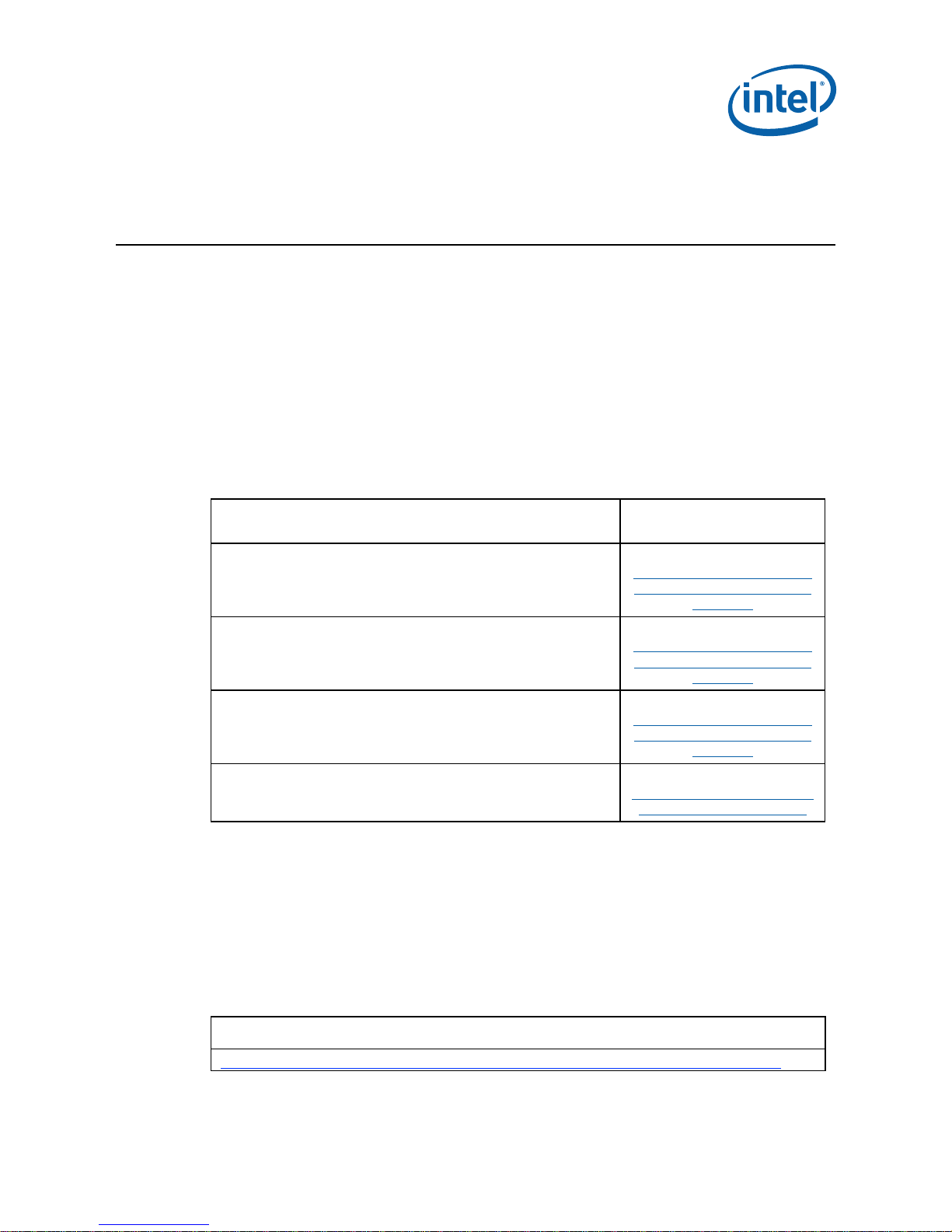
Affected Documents
Document Title Document
Intel® Pentium® 4 Processor in the 423-pin Package
datasheet
Intel® Pentium® 4 Processor in the 478-pin Package
datasheet
Intel® Pentium® 4 Processor with 512-KB L2 Cache on 0.13
Micron Process and In te l
Edition Supportin g H y p e r-Thre a d in g Tech nology
Intel® Pentium® 4 Processor Extreme Edition on 0.13 Micron
Process in the 775-land Package datasheet
NOTES:
1. Hyper-Threading Technology requires a computer system with an Intel
processor supporting HT Technology and a Hyper-Threading Technology enabled
chipset, BIOS and operating system. Performance will vary depending on the specific
hardware and software you use. See <<http:// www.intel.com/info/hyperthreading/>>
for more information including details on which processors support HT Technology.
®
Pentium® 4 Processor Extreme
1
datasheet
Number/Location
http://developer.intel.com/d
esign/pentium4/datashts/24
http://developer.intel.com/d
esign/pentium4/datashts/24
http://developer.intel.com/d
esign/pentium4/datashts/29
http://intel.com/design/Penti
um4/datashts/302351.htm
249198-005
9198.htm
249887-003
9887.htm
298643-012
8643.htm
302350-001
®
Pentium® 4
Related Documents
Intel® 64 and IA-32 Intel Architectures Software Developer's Manual Volume 1: Basic
Specification Update 9
Document Title and Link
Page 10

Architecture
Intel® 64 and IA-32 Intel Architectures Software Developer's Manual Volume 2A:
Instruction Set Reference, A-M
Intel® 64 and IA-32 Intel Architectures Software Developer's Manual Volume 2B:
Instruction Set Reference, N-Z
Intel® 64 and IA-32 Intel Architectures Software Developer's Manual Volume 3A: System
Programming Guide
Intel® 64 and IA-32 Intel Architectures Software Developer's Manual Volume 3B: System
Programming Guide
Nomenclature
Preface
Document Title and Link
Errata are design defects or errors. Errata may cause the Intel
®
Pentium® 4
processor’s behavior to deviate from published specifications. Hardware and software
designed to be used with any given stepping must assume that all errata
documented for that stepping are present on all devices.
Specification Changes are modifications to the current published specifications.
These changes will be incorporated in the next release of the specifications.
Specification Clarifications describe a specification in greater detail or further
highlight a specification’s impact to a complex design situation. These clarifications
will be incorporated in the next release of the specifications.
Documentation Changes include typos, errors, or omissions from the current
published specifications. These changes will be incorporated in the next release of the
specifications.
Note: Errata remain in the specification update throughout the product’s lifecycle, or until a
particular stepping is no longer commercially available. Under these circumstances,
errata removed from the specification update are archived and available upon
request. Specification changes, specification clarifications and documentation
changes are removed from the specification update when the appropriate changes
are made to the appropriate product specification or user documentation
(datasheets, manuals, etc.).
§
10 Specification Update
Page 11

Summary Tables of Changes
Summary Tables of Changes
The following table indicates the Specification Changes, Errata, Specification
Clarifications or Documentation Changes, which apply to the listed MCH steppings.
Intel intends to fix some of the errata in a future stepping of the component, and to
account for the other outstanding issues through documentation or Specification
Changes as noted. This table uses the following notations:
Codes Used in Summary Table
Stepping
X: Erratum, Specification Change or Clarification that applies
to this stepping.
Status
Row
Note: Each Specification Update item is prefixed with a capital letter to distinguish the
(No mark) or (Blank Box): This erratum is fixed in listed stepping or specification
change does not apply to listed stepping.
Doc: Document change or update that will be implemented.
PlanFix: This erratum may be fixed in a future stepping of the
product.
Fixed: This erratum has been previously fixed.
NoFix: There are no plans to fix this erratum.
Shaded: This item is either new or modified from the previous
version of the document.
product. The key below details the letters that are used in Intel’s microprocessor
Specification Updates:
A = Dual-Core Intel® Xeon® processor 7000 sequence
C = Intel® Celeron® processor
D = Dual-Core Intel® Xeon® processor 2.80 GHz
Specification Update 11
Page 12

Summary Tables of Changes
E = Intel® Pentium® III processor
F = Intel® Pentium® processor Extreme Edition and Intel® Pentium® D
processor
I = Dual-Core Intel® Xeon® processor 5000 series
J = 64-bit Intel® Xeon® processor MP with 1MB L2 cache
K = Mobile Intel® Pentium® III processor
L = Intel® Celeron® D processor
M = Mobile Intel® Celeron® processor
N = Intel® Pentium® 4 processor
O = Intel® Xeon® processor MP
P = Intel ® Xeon® processor
Q = Mobile Intel® Pentium® 4 processor supporting Hyper-Threading technology
on 90-nm process technology
R = Intel® Pentium® 4 processor on 90 nm process
S = 64-bit Intel® Xeon® processor with 800 MHz system bus (1 MB and 2 MB L2
cache versions)
T = Mobile Intel® Pentium® 4 processor-M
U = 64-bit Intel® Xeon® processor MP with up to 8MB L3 cache
V = Mobile Intel® Celeron® processor on .13 micron process in Micro-FCPGA
package
W= Intel® Celeron® M processor
X = Intel® Pentium® M processor on 90nm process with 2-MB L2 cache and
Intel® processor A100 and A110 with 512-KB L2 cache
Y = Intel® Pentium® M processor
Z = Mobile Intel® Pentium® 4 processor with 533 MHz system bus
AA = Intel® Pentium® D processor 900 sequence and Intel® Pentium® processor
Extreme Edition 955, 965
AB = Intel® Pentium® 4 processor 6x1 sequence
AC = Intel(R) Celeron(R) processor in 478 pin package
AD = Intel(R) Celeron(R) D processor on 65nm process
AE = Intel® Core™ Duo processor and Intel® Core™ Solo processor on 65nm
process
AF = Dual-Core Intel® Xeon® processor LV
AG = Dual-Core Intel® Xeon® processor 5100 series
AH = Intel® Core™2 Duo/Solo processor for Intel® Centrino® Duo processor
technology
AI = Intel® Core™2 Extreme processor X6800 and Intel® Core™2 Duo desktop
processor E6000 and E4000 sequence
12 Specification Update
Page 13
Summary Tables of Changes
AJ = Quad-Core Intel® Xeon® processor 5300 series
AK = Intel® Core™2 Extreme quad-core processor QX6000 sequence and Intel®
Core™2 Quad processor Q6000 sequence
AL = Dual-Core Intel® Xeon® processor 7100 series
AM = Intel® Celeron® processor 400 sequence
AN = Intel® Pentium® dual-core processor
AO = Quad-Core Intel® Xeon® processor 3200 series
AP = Dual-Core Intel® Xeon® processor 3000 series
AQ = Intel® Pentium® dual-core desktop processor E2000 sequence
AR = Intel® Celeron® processor 500 series
AS = Intel® Xeon® processor 7200, 7300 series
AT = Intel® Celeron® processor 200 series
AU = Intel® Celeron® Dual Core processor T1400
AV = Intel® Core™2 Extreme processor QX9650 and Intel® Core™2 Quad
processor Q9000 series
AW = Intel® Core™ 2 Duo processor E8000 series
AX = Quad-Core Intel® Xeon® processor 5400 series
AY= Dual-Core Intel® Xeon® processor 5200 series
AZ = Intel® Core™2 Duo Processor and Intel® Core™2 Extreme Processor on 45-
nm Process
AAA = Quad-Core Intel® Xeon® processor 3300 series
AAB = Dual-Core Intel® Xeon® E3110 Processor
AAC = Intel® Celeron® dual-core processor E1000 series
AAD = Intel® Core™2 Extreme Processor QX9775Δ
AAE = Intel® Atom™ processor Z5xx series
AAF = Intel® Atom™ processor 200 series
AAG = Intel® Atom™ processor N series
No. B2 C1 D0 E0 B0 C1 D1 M0 Plan ERRATA
I/O restart in SMM may fail after
N1 X X X X X X X X No Fix
N2 X X X X X X X X No Fix
simultaneous machine check exception
(MCE)
MCA registers may contain invalid
information if RESET# occurs and
PWRGOOD is not held asserted
Specification Update 13
Page 14

Summary Tables of Changes
No. B2 C1 D0 E0 B0 C1 D1 M0 Plan ERRATA
Uncacheable (UC) code in same line as
N3 X X X X Fixed
N4 X X X X X X X X No Fix Transaction is not retried after BINIT#
N5 X X X X X X X X No Fix
N6 X Fixed
N7 X Fixed
N8 X X X X X X X X No Fix
N9 X X X X X X X X No Fix
N10 X Fixed
N11 X Fixed
N12 X X X X X X X X No Fix
N13 X X X X X X X X No Fix
N14 X Fixed
N15 X X X X Fixed
N16 X X X X Fixed
N17 X X X X Fixed
N18 X Fixed
N19 X Fixed
N20 X X X X Fixed
write back (WB) data may lead to data
corruption
Invalid opcode 0FFFh requires a ModRM
byte
RFO-ECC-snoop-MCA combination can
result in two lines being corrupted in
main memory
Overlap of MTRRs with the same
memory type results in a type of
uncacheable (UC)
FSW may not be completely restored
after page fault on FRSTOR or FLDENV
instructions
The Proce sso r Signals Pa ge-Fault Excep t ion
(#PF) Instead of Alignment Check Exception
(#AC) on an Unlocked CMPXCHG8B
Instruction
IERR# may not go active when an
internal error occurs
All L2 cache uncorrectable errors are
logged as data writes
When in no-fill mode the memory type
of large pages are incorrectly forced to
uncacheable
Processor may hang due to speculative
page walks to non-existent system
memory
Load operations may get stale data in
the presence of memory address
aliasing
Writing a performance counter may
result in incorrect value
IA32_MC0_STATUS register overflow
bit not set correctly
Performance counter may contain
incorrect value after being stopped
The TAP drops the last bit during
instruction register shifting
Data breakpoints on the high half of a
floating point line split may not be
captured
MCA error code field in
IA32_MC0_STATUS register may
become out of sync with the rest of the
14 Specification Update
Page 15

Summary Tables of Changes
No. B2 C1 D0 E0 B0 C1 D1 M0 Plan ERRATA
register
N21 X Fixed
N22 X X X X X X X X No Fix
N23 X Fixed
N24 X Fixed
N25 X Fixed
N26 X Fixed
N27 X Fixed
N28 X Fixed
N29 X X Fixed
N30 X Fixed
N31 X Fixed
N32 X Fixed
N33 X Fixed
N34 X Fixed
N35 X Fixed
N36 X X Fixed
N37 X X X X X X X X No Fix
N38 X X X X X X X X No Fix
Processor may hang on a correctable
error and snoop combination
The IA32_MC1_STATUS register may
contain incorrect information for
correctable errors
MCA error incorrectly logged as
prefetches
Speculative loads which hit the L2
cache and get an uncorrectable error
will log erroneous information
Processor may fetch reset vector from
cache if A20M# is asserted during init
A correctable error on an L2 cache
shared state line hit with go to invalid
snoop hangs processor
System hang due to uncorrectable
error and bus lock combination
Incorrect address for an L1 tag parity
error is logged in IA32_MC1_ADDR
register
REP MOV instruction with overlapping
source and destination may result in
data corruption
Stale data in processor translation
cache may result in hang
I/O buffers for FERR#, PROCHOT# and
THERMTRIP# are not AGTL+
RFO and correctable error combination
may cause lost store or hang
RFO and correctable error may
incorrectly signal the machine check
handler
Processor may report invalid TSS fault
instead of double fault during mode C
paging
IA32_MC0_STATUS incorrect after
illegal APIC request
Thermal status log bit may not be set
when the thermal control circuit is
active
Debug mechanisms may not function
as expected
Machine check architecture error
reporting and recovery may not work
Specification Update 15
Page 16

Summary Tables of Changes
No. B2 C1 D0 E0 B0 C1 D1 M0 Plan ERRATA
as expected
N39 X X X X Fixed
N40 X X X X X X X X No Fix
N41 X Fixed
N42 X X X X Fixed
N43 X X X X X X X X No Fix
N44 X X X X Fixed
N45 X X Fixed
N46 X X Fixed
N47 X X X Fixed
N48 X X X X Fixed
N49 X X X X Fixed
N50 X X X X X Fixed
N51 X X X Fixed
N52 X X X X X X X X No Fix
N53 X X X X X Fixed
N54 X X X X Fixed
N55 X X X X X X X X No Fix
Processor may Timeout Waiting for a
Device to Respond after ~0.67 Seconds
Cascading of Performance Counters
does not work Correctly when Forced
Overflow is Enabled
Possible Machine Check Due to LineSplit Loads with Page-Tables in
Uncacheable (UC) Space
IA32_MC1_STATUS MSR ADDRESS
VALID bit may be set when no Valid
Address is Available
EMON event counting of x87 loads may
not work as expected
Software controlled clock modulation
using a 12.5% or 25% duty cycle may
cause the processor to hang
Speculative page fault may cause
livelock
PAT index MSB may be calculated
incorrectly
SQRTPD and SQRTSD may return
QNaN indefinite instead of negative
zero
Bus invalidate line requests that return
unexpected data may result in L1
cache corruption
Write Combining (WC) load may result
in unintended address on system bus
Incorrect data may be returned when
page tables are in Write Combining
(WC) memory space
Buffer on resistance may exceed
specification
Processor issues inconsistent
transaction size attributes for locked
operation
Multiple accesses to the same S-state
L2 cache line and ECC error
combination may result in loss of cache
coherency
Processor may hang when resuming
from Deep Sleep state
When the processor is in the System
Management Mode (SMM), debug
registers may be fully writeable
16 Specification Update
Page 17
Summary Tables of Changes
No. B2 C1 D0 E0 B0 C1 D1 M0 Plan ERRATA
Associated counting logic must be
N56 X X X X Fixed
configured when using Event Selection
Control (ESCR) MSR
IA32_MC0_ADDR and IA32_MC0_MISC
N57 X X X X X X X X No Fix
registers will contain invalid or stale
data following a Data, Address, or
Response Parity Error
CR2 may be incorrect or an incorrect
N58 X X X X X Fixed
page fault error code may be pushed
onto stack after execution of an LSS
instruction
N59 X Fixed
BPM[5:3]# V
specification
does not meet
IL
Processor may hang under certain
N60 X X X X No Fix
frequencies and 12.5% STPCLK# duty
cycle
System may hang if a fatal cache error
causes Bus Write Line (BWL)
N61 X X X X X X X X No Fix
transaction to occur to the same cache
line address as an outstanding Bus
Read Line (BRL) or Bus Read-Invalidate
Line (BRIL)
N62 X X X X X Fixed
L2 cache may contain stale data in the
Exclusive state
Re-mapping the APIC base address to
N63 X X X X X X Fixed
a value less than or equal to
0xDC001000 may cause IO and Special
Cycle failure
N64 X X X Fixed
N65 X X X X X Fixed
Erroneous BIST result found in EAX
register after reset
Processor does not flag #GP on nonzero write to certain MSRs
Simultaneous assertion of A20M# and
N66 X X X X X X X X No Fix
INIT# may result in incorrect data
fetch
N67 X X X X X Fixed
N68 X X X X X X X X No Fix
N69 X X
Plan
Fix
N70 X Fixed
N71 X X X X No Fix
CPUID instruction returns incorrect
number of ITLB entries
A Write to an APIC Register Sometimes May
Appear to Have Not Occurred
STPCLK# Signal Assertion under
Certain Conditions May Cause a
System Hang
Store to Load Data Forwarding may
Result in Switched Data Bytes
Parity Error in the L1 Cache may Cause
the Processor to Hang
Specification Update 17
Page 18

Summary Tables of Changes
No. B2 C1 D0 E0 B0 C1 D1 M0 Plan ERRATA
The TCK Input in the Test Access Port
N72 X X Fixed
N73 X X X No Fix
N74 X X
N75 X X X No Fix
N76 X X X X X X No Fix
N77 X X X X X X X X No Fix
N78 X X X X X X X X No Fix
N79 X X1 X1
N80 X X X X X X X X No Fix
N81 X X X X X X X X No Fix
N82 X X X No Fix
N83 X X X X X X X X
N84 X
N85 X X X No Fix
Plan
Fix
Plan
Fix
Plan
Fix
Plan
Fix
(TAP) is Sensitive to Low Clock Edge
Rates and Prone to Noise Coupling
Onto TCK's Rising or Falling Edges
Disabling a Local APIC Disables Both
Logical Processor APICs on a HyperThreading Technology Enabled
Processor
A circuit marginality in the 800 MHz
Front Side Bus power save circuitry
may cause a system and/or application
hang or may result in incorrect data
Using STPCLK# and Executing Code
From Very Slow Memory Could Lead to
a System Hang
Changes to CR3 Register do not Fence
Pending Instruction Page Walks
The State of the Resume Flag (RF Flag)
in a Task-State Segment (TSS) May be
Incorrect
Processor Provides a 4-Byte Store
Unlock After an 8-Byte Load Lock
Simultaneous Page Faults at Similar
Page Offsets on Both Logical Processors
of an Hyper-Threading Technology
Enabled Processor May Cause
Application Failure
System Bus Interrupt Messages
Without Data Which Receive a
HardFailure Response May Hang the
Processor
Memory Type of the Load Lock
Different from its Corresponding Store
Unlock
Shutdown and IERR# May Result Due
to a Machine Check Exception on a
Hyper-Threading Technology Enabled
Processor
A 16-bit Address Wrap Resulting from
a Near Branch (Jump or Call) May
Cause an Incorrect Address to Be
Reported to the #GP Exception Handler
Simultaneous Cache Line Eviction From
L2 and L3 Caches may Result in the
Write Back of Stale Data
Locks and SMC Detection May Cause
the Processor to Temporarily Hang
18 Specification Update
Page 19

Summary Tables of Changes
No. B2 C1 D0 E0 B0 C1 D1 M0 Plan ERRATA
Incorrect Debug Exception (#DB) May
N86 X X X X X X X X No Fix
Occur When a Data Breakpoint is set
on an FP Instruction
N87 X
Plan
Fix
N88 X X X X X X X X No Fix
Modified Cache Line Eviction From L2
Cache May Result in Writeback of Stale
Data
xAPIC Ma y Not Report Some Illegal Vector
Errors
Incorrect Duty Cycle is Chosen whe n On-
N89 X X X
Plan
Fix
Demand Clock Modula tion is Enabled in a
Processor Supporting Hyper-Threading
Technology
Memory Aliasing of Pages as Uncacheable
N90 X X X X X X X X No Fix
Memory Type and Write Back (WB) May Hang
the System
N91 X X
Plan
Fix
N92 X X X No Fix
N93 X X X X X X X X No Fix
A Timing Marginality in the Instruction Decode r
Unit May Cause an Unpredictable Applicatio n
Behav ior and/or System Hang
Missing Stop Gran t Ackn owledge Special Bus
Cycle May Cause a System Hang
Check Exceptions May not Update LastExcept ion Record MSRs (LERs)
Stores to Page Tab l es May Not Be Visible to
N94 X X X X X X X X No Fix
Pagewalks for Subsequent Loads Without
Serializing or Inv alidating the Page Table Entry
N95 X X
Plan
Fix
A Timing Marginality in the Arithmetic Lo gic
Unit (ALU) May Cause Indeterminate Behavior
With TF (Trap Flag) Asserted , F P I nstruction
N96 X X X X X X X X No Fix
That Triggers an Unmasked FP Exception
May Take Sing le Step Tra p Before Retirement
of Instruction
BTS(Branch Trace Store) an d PEBS(Precise
N97 X X X X X X X X No Fix
Event Based Sampling) May Update Memory
outside the BTS/PEBS Buffer
Brand String Field Reports Incorrect Maximum
N98 X No Fix
Operating Frequency on Intel
Extreme Edition Proce ssor with 1066 MHz
®
FSB
Memory Ordering Failure May Occur wi th
Snoop Filtering Third Party Agents after
N99 X X X X X X X X No Fix
Issuing and Completing a BWIL (Bus Write
Invalidate Line) or BLW (Bus Locked Write)
Transaction
Control Register 2 (CR2) Can be Updated
N100 X X X X X X X X No Fix
during a REP MOVS/STOS Instruction with
Fast Strings Enabled
N101 X X X X X X X X No Fix
Writing the Local Vector Table (LVT)
Pentium® 4
Specification Update 19
Page 20
Summary Tables of Changes
No. B2 C1 D0 E0 B0 C1 D1 M0 Plan ERRATA
when an Interrupt is Pending May Cause an
Unexpected Interrupt
Using 2M/4M Pages When A20M# Is
N102 X X X X X X X X No Fix
N103 X X X X X X X X No Fix
N104 X X X X X X X X No Fix
NOTE:
1. For these steppings, this erratum may be worked around in BIOS.
Asserted May Result in Incorrect
Address Translations
Writing Shared Unaligned Data that
Crosses a Cache Line without Proper
Semaphores or Barriers May Expose a
Memory Ordering Issue
Debug Status Register (DR6)
Breakpoint Condition Detected Flags
May be set Incorrectly
No. B2 C1 D0 E0 B0 C1 D1 M0 Plans SPECIFICATION CHANGES
There are no specification changes in
this Specification Update revision.
No. B2 C1 D0 E0 B0 C1 D1 M0 Plans SPECIFICATION CLARIFICATIONS
N1 X X X X X X X X Doc
Specification clarification with respect
to time stamp counter
No. B2 C1 D0 E0 B0 C1 D1 M0 Plans DOCUMENTATION CHANGES
There are no Documentation Changes
in this Specification Update revision.
§
20 Specification Update
Page 21
m ©
-
m ©
S -
S -
2 -
2 -
General Information
General Informa ti o n
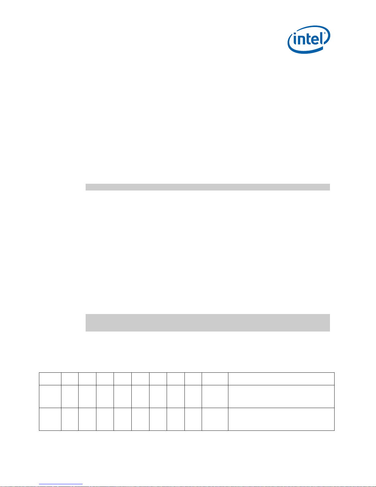
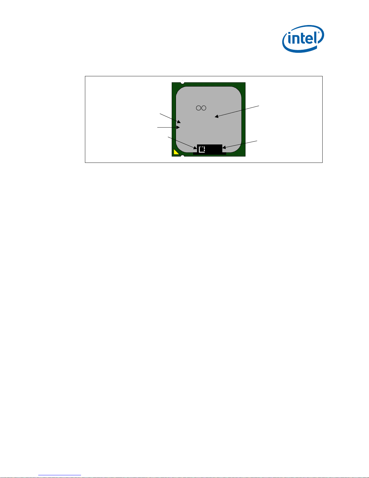
Figure 1 Intel® Pentium® 4 Processor in the 423-Pin Package and Boxed Pentium 4
Processor in the 423-Pin Package Markings
Frequency/Cache/Bus/Voltage
2-D Matrix Mark
S-Spec/Country of Assy
FPO - Serial #
®
®
Intel
Intel
®bbb
pentium
pentium
1.5GHz/256/400/1.7V
1.5GHz/256/400/1.7V
SL4SH MALAY
SYYYY XXXXXX
1234567
FFFFFFFF-NNNN
i m c ‘00
i m c ‘00
®bbb
-1272
8
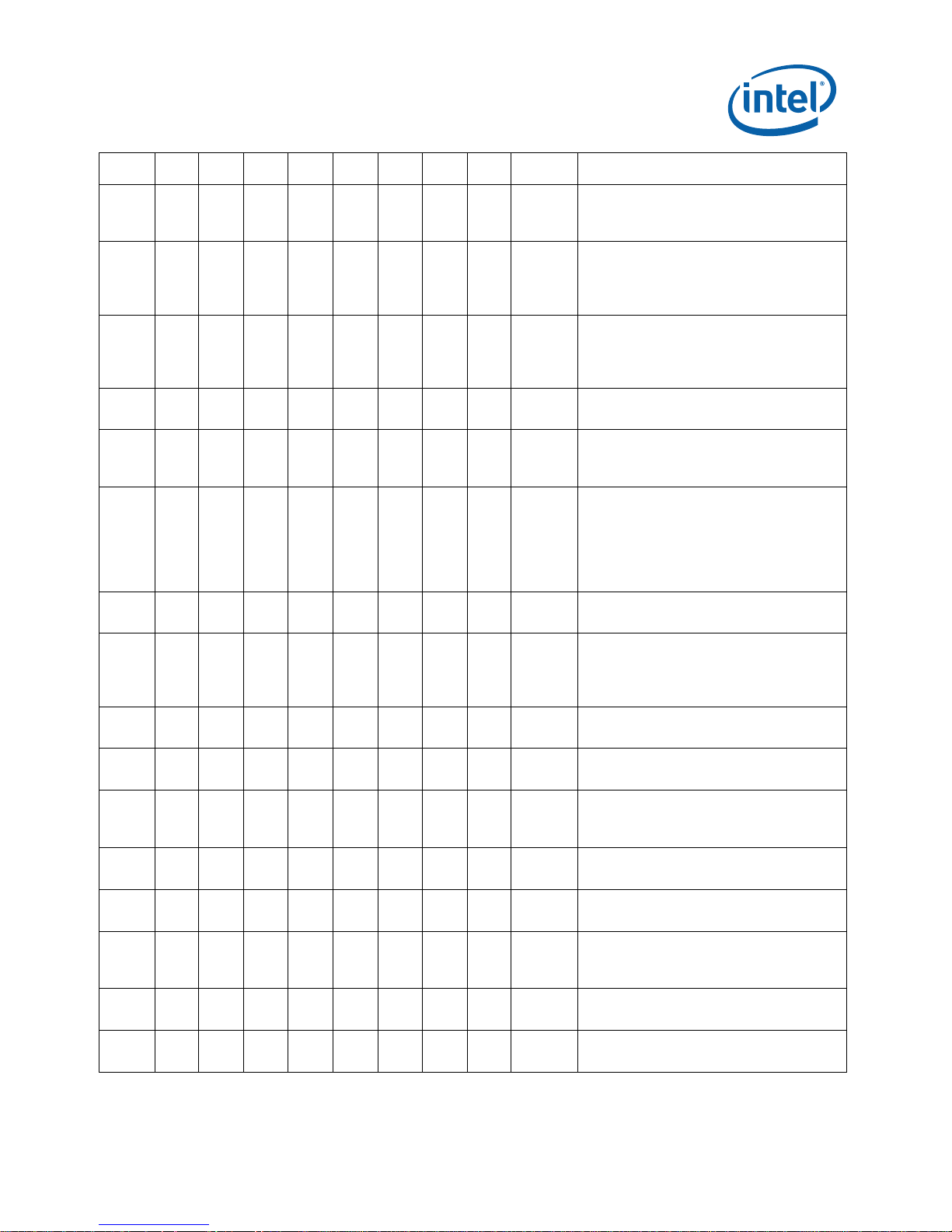
Figure 2 Intel® Pentium® 4 Processor in the 478-Pin Package Markings Example 1
S-Spec/Count ry of Assy
2
Frequency/Cache/Bus/Voltage
GHZ/256/400/1.75V
SYYYY XXXXXX
FPO - Serial #
FFFFFFFF-NNNN
i ©‘01
2-D Matr ix Mark
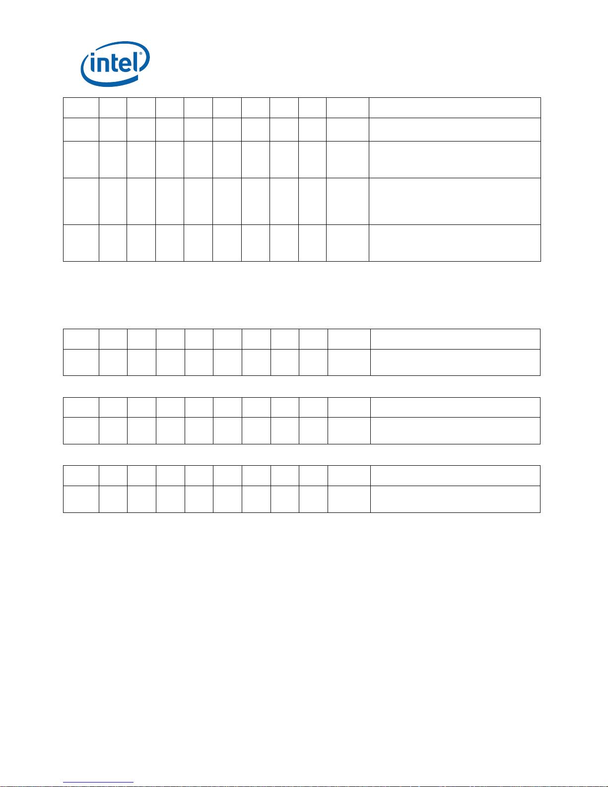
Figure 3 Pentium 4 Processor in the 478-Pin Package Markings Example 2
Spec/Country of Assy
Spec/Country of Assy
FPO - Serial #
FPO - Serial #
D Matrix Mark
D Matrix Mark
Specification Update 21
‘02
i
PENTIUM® 4
2A GHZ/512/400/1.50V
2 GHZ/256/400/1.75V
SYYYY XXXXXX
SYYYY XXXXXX
FFFFFFFF - NNNN
FFFFFFFF
i
‘01
NNNN
Frequency/Cache/Bus/Voltage
Frequency/Cache/Bus/Voltage
Page 22

General Information
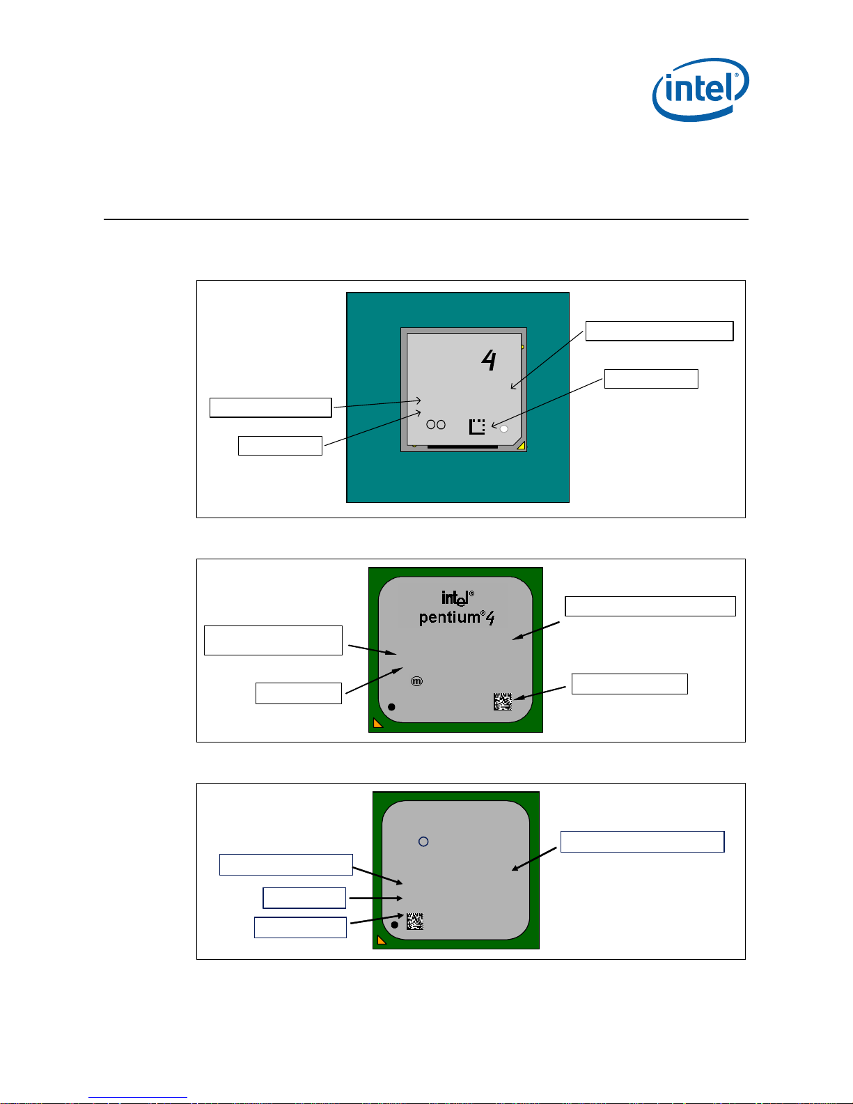
Figure 4 Intel® Pentium® 4 Processor with 512-KB L2 Cache on 0.13 Micron Process,
Intel
®
Pentium® 4 Processor Extreme Edition Supporting Hyper-Threading
Technology, and Boxed Pentium 4 Processor with 512-KB L2 Cache on 0.13
Micron Process Processor Markings
m c
`01
Frequency/Cache/Bus/Voltage
2-D Matr ix Mark
S-Spec /C ountry of Assy
FPO – Ser ial #
INTEL
PENTIUM® 4
2.40 GHZ/512/800/1.50V
SYYYY XXXXXX
FFFFFFFF–NNNN
Figure 5 Multiple VIDs Example 1
mc
`03
AAAAAAAA
NNNN
Frequency/Cache/Bus
unique unit identifier
ATPO
Serial #
S-Spec/Country of Assy
FPO
2-D Matrix Mark
INTEL
PENTIUM® 4
2.40 GHZ/512/800
SYYYY XXXXXX
FFFFFFFF
Figure 6 Multiple VIDs Example 2
m c
`01
Frequency/Cache/Bus
2-D Matrix Mark
S-Spec/Country of Assy
FPO – Serial #
INTEL
PENTIUM® 4
2.40 GHZ/512/800
SYYYY XXXXXX
FFFFFFFF–NNNN
22 Specification Update
Page 23
General Information
Figure 7 Intel® Pentium® 4 Extreme Edition on 0.13 micron in the 775-Land LGA
Package Marking
Frequency/
S-Spec/
Country of Assy
FPO
2-D Matrix Mark
m c
INTEL
PENTIUM®4
3.40 GHZ/512/800
SYYYY XXXXXX
FFFFFFFF
`04
ATTPO
S/N
L2 Cache/
Bus
Uniqu e Un it
Identifier
ATPO
Serial #
Specification Update 23
Page 24

Identification Informati o n
The Pentium 4 processor may be identified by the following component markings:
Family1 Model2 Brand ID3
1111 0000 00001000
1111 0001 00001000 or 00001001
1111 0010 00001001
1111 0011 —
NOTES:
1. The Family corresponds to bits [11:8] of the EDX register after RESET, bits [11:8] of
the EAX register after the CPUID instruction is executed with a 1 in the EAX register,
and the generation field of the Device ID registers accessible through Boundary Scan.
2. The Model corresponds to bits [7:4] of the EDX register after RESET, bits [7:4] of the
EAX register after the CPUID instruction is executed with a 1 in the EAX register, and
the model field of the Device ID registers accessible through Boundary Scan.
3. The Brand ID corresponds to bits [7:0] of the EBX register after the CPUID instruction is
executed with a 1 in the EAX register.
Identification Information
Table 1. Intel® Pentium® 4 Processor Identifi cation Information
S-Spec
SL4QD B2 256K 0F07h 1.30GHz/400MHz 31.0 mm OOI rev 1.0 1, 3
SL4SF B2 256K 0F07h 1.30GHz/400MHz 31.0 mm OOI rev 1.0 3
SL4SG B2 256K 0F07h 1.40GHz/400MHz 31.0 mm OOI rev 1.0 2, 3
SL4SC B2 256K 0F07h 1.40GHz/400MHz 31.0 mm OOI rev 1.0 1, 3
SL4SH B2 256K 0F07h 1.50GHz/400MHz 31.0 mm OOI rev 1.0 2, 3
SL4TY B2 256K 0F07h 1.50GHz/400MHz 31.0 mm OOI rev 1.0 1, 3
SL5FW C1 256K 0F0Ah 1.30GHz/400MHz 31.0 mm OOI rev 1.0 3
SL4WS C1 256K 0F0Ah 1.40GHz/400MHz 31.0 mm OOI rev 1.0 3
SL4WT C1 256K 0F0Ah 1.50GHz/400MHz 31.0 mm OOI rev 1.0 3
SL4WU C1 256K 0F0Ah 1.60GHz/400MHz 31.0 mm OOI rev 1.0 3
SL57W C1 256K 0F0Ah 1.7GHz/400MHz 31.0 mm OOI rev 1.0 2, 3
SL4WV C1 256K 0F0Ah 1.80GHz/400MHz 31.0 mm OOI rev 1.0 3
SL5GC C1 256K 0F0Ah 1.30GHz/400MHz 31.0 mm OOI rev 1.0 1, 3
SL4X2 C1 256K 0F0Ah 1.40GHz/400MHz 31.0 mm OOI rev 1.0 1, 3
SL4X3 C1 256K 0F0Ah 1.50GHz/400MHz 31.0 mm OOI rev 1.0 1, 3
Core
Stepping
L2 Cache
Size (bytes)
CPUID Speed Core/Bus Package and Revision Notes
24 Specification Update
Page 25

Identification Information
S-Spec
SL4X4 C1 256K 0F0Ah 1.60GHz/400MHz 31.0 mm OOI rev 1.0 1, 3
SL57V C1 256K 0F0Ah 1.70GHz/400MHz 31.0 mm OOI rev 1.0 1, 3
SL4X5 C1 256K 0F0Ah 1.80GHz/400MHz 31.0 mm OOI rev 1.0 1, 3
SL5SX D0 256K 0F12h 1.50GHz/400MHz 31.0 mm FC rev 1.0 3
SL5VL D0 256K 0F12h 1.60GHz/400MHz 31.0 mm FC rev 1.0 3
SL5SY D0 256K 0F12h 1.70GHz/400MHz 31.0 mm FC rev 1.0 3
SL5VM D0 256K 0F12h 1.80GHz/400MHz 31.0 mm FC rev 1.0 3
SL5VN D0 256K 0F12h 1.90GHz/400MHz 31.0 mm FC rev 1.0 3
SL5SZ D0 256K 0F12h 2GHz/400MHz 31.0 mm FC rev 1.0 3
SL5UL D0 256K 0F12h 1.60GHz/400MHz 31.0 mm OOI rev 1.0 1, 3
SL5VM D0 256K 0F12h 1.80GHz/400MHz 31.0 mm OOI rev 1.0 1, 3
SL5WH D0 256K 0F12h 1.90GHz/400MHz 31.0 mm OOI rev 1.0 1, 3
SL5TQ D0 256K 0F12h 2GHz/400MHz 31.0 mm OOI rev 1.0 1, 3
SL59U C1 256K 0F0Ah 1.40GHz/400MHz 31.0 mm FC rev 1.0 2, 4
SL59V C1 256K 0F0Ah 1.50GHz/400MHz 31.0 mm FC rev 1.0 4
SL5US C1 256K 0F0Ah 1.60GHz/400MHz 31.0 mm FC rev 1.0 4
SL59X C1 256K 0F0Ah 1.70GHz/400MHz 31.0 mm FC rev 1.0 4
SL5UT C1 256K 0F0Ah 1.80GHz/400MHz 31.0 mm FC rev 1.0 4
SL5VK D0 256K 0F12h 1.90GHz/400MHz 31.0 mm FC rev 1.0 4
SL5TG D0 256K 0F12h 1.40GHz/400MHz 31.0 mm FC rev 1.0 2, 4
SL5TJ D0 256K 0F12h 1.50GHz/400MHz 31.0 mm FC rev 1.0 2, 4
SL5VH D0 256K 0F12h 1.60GHz/400MHz 31.0 mm FC rev 1.0 2, 4
SL5TK D0 256K 0F12h 1.70GHz/400MHz 31.0 mm FC rev 1.0 2, 4
SL5VJ D0 256K 0F12h 1.80GHz/400MHz 31.0 mm FC rev 1.0 2, 4
SL5VK D0 256K 0F12h 1.90GHz/400MHz 31.0 mm FC rev 1.0 2, 4
SL5TL D0 256K 0F12h 2GHz/400MHz 31.0 mm FC rev 1.0 4
SL5N7 C1 256K 0F0Ah 1.40GHz/400MHz 31.0 mm FC rev 1.0 1, 4
SL5N8 C1 256K 0F0Ah 1.50GHz/400MHz 31.0 mm FC rev 1.0 1, 4
SL5UW C1 256K 0F0Ah 1.60GHz/400MHz 31.0 mm FC rev 1.0 1, 4
SL5N9 C1 256K 0F0Ah 1.70GHz/400MHz 31.0 mm FC rev 1.0 1, 4
SL5UV C1 256K 0F0Ah 1.80GHz/400MHz 31.0 mm FC rev 1.0 1, 4
SL5UE D0 256K 0F12h 1.40GHz/400MHz 31.0 mm FC rev 1.0 1, 4
SL5UF D0 256K 0F12h 1.50GHz/400MHz 31.0 mm FC rev 1.0 1, 4
SL62Y D0 256K 0F12h 1.50GHz/400MHz 31.0 mm FC rev 1.0 1, 4, 6
Core
Stepping
L2 Cache
Size (bytes)
CPUID Speed Core/Bus Package and Revision Notes
Specification Update 25
Page 26

Identification Information
S-Spec
SL5UJ D0 256K 0F12h 1.60GHz/400MHz 31.0 mm FC rev 1.0 1, 4
SL5UG D0 256K 0F12h 1.70GHz/400MHz 31.0 mm FC rev 1.0 1, 4
SL62Z D0 256K 0F12h 1.70GHz/400MHz 31.0 mm FC rev 1.0 1, 4, 7
SL5UK D0 256K 0F12h 1.80GHz/400MHz 31.0 mm FC rev 1.0 1, 4
SL5WG D0 256K 0F12h 1.90GHz/400MHz 31.0 mm FC rev 1.0 1, 4
SL668 B0 512K 0F24h 1.60GHz/400MHz 31.0 mm FC rev 1.0 1, 5, 8
SL63X B0 512K 0F24h 1.80GHz/400MHz 31.0 mm FC rev 1.0 1, 5, 9
SL62P B0 512K 0F24h 1.80GHz/400MHz 31.0 mm FC rev 1.0 2, 5, 7, 9
SL68Q B0 512K 0F24h 1.80GHz/400MHz 31.0 mm FC rev 1.0 1, 5
SL68R B0 512K 0F24h 2GHz/400MHz 31.0 mm FC rev 1.0 1, 5
SL5YR B0 512K 0F24h 2GHz/400MHz 31.0 mm FC rev 1.0 2, 5
SL5YS B0 512K 0F24h 2.20GHz/400MHz 31.0 mm FC rev 1.0 2, 5
SL68S B0 512K 0F24h 2.20GHz/400MHz 31.0 mm FC rev 1.0 1, 5
SL68T B0 512K 0F24h 2.40GHz/400MHz 31.0 mm FC rev 1.0 1, 5
SL5ZU B0 512K 0F24h 2.20GHz/400MHz 31.0 mm FC rev 1.0 1, 5
SL65R B0 512K 0F24h 2.40GHz/400MHz 31.0 mm FC rev 1.0 2, 5
SL67R B0 512K 0F24h 2.40GHz/400MHz 31.0 mm FC rev 1.0 1, 5
SL683 B0 512K 0F24h 2.26GHz/533MHz 31.0 mm FC rev 1.0 1, 5
SL67Y B0 512K 0F24h 2.26GHz/533MHz 31.0 mm FC rev 1.0 2, 5
SL684 B0 512K 0F24h 2.40GHz/533MHz 31.0 mm FC rev 1.0 1, 5
SL67Z B0 512K 0F24h 2.40GHz/533MHz 31.0 mm FC rev 1.0 2, 5
SL685 B0 512K 0F24h 2.53GHz/533MHz 31.0 mm FC rev 1.0 1, 5
SL682 B0 512K 0F24h 2.53GHz/533MHz 31.0 mm FC rev 1.0 2, 5
SL6HL C1 512K 0F27h 2.80GHz/533MHz 31.0 mm FC rev 1.0 5
SL6K6 C1 512K 0F27h 2.80GHz/533MHz 31.0 mm FC rev 1.0 1, 5
SL6LA C1 512K 0F27h 1.80GHz/400MHz 31.0 mm FC rev 1.0 5
SL6GQ C1 512K 0F27h 2GHz/400MHz 31.0 mm FC rev 1.0 5
SL6GR C1 512K 0F27h 2.2GHz/400MHz 31.0 mm FC rev 1.0 5
SL6DU C1 512K 0F27h 2.26GHz/533MHz 31.0 mm FC rev 1.0 5
SL6EF C1 512K 0F27h 2.40GHz/533MHz 31.0 mm FC rev 1.0 1, 5
SL6DV C1 512k 0F27h 2.40GHz/533MHz 31.0 mm FC rev 1.0 2, 5
SL6EG C1 512K 0F27h 2.53GHz/533MHz 31.0 mm FC rev 1.0 1, 5
SL6DW C1 512K 0F27h 2.53GHz/533MHz 31.0 mm FC rev 1.0 2, 5
SL6S6 C1 512K 0F27h 1.80GHz/400MHz 31.0 mm FC rev 1.0 5, 16
Core
Stepping
L2 Cache
Size (bytes)
CPUID Speed Core/Bus Package and Revision Notes
26 Specification Update
Page 27

Identification Information
S-Spec
SL6S7 C1 512K 0F27h 2.00GHz/400MHz 31.0 mm FC rev 1.0 5, 16
SL6S8 C1 512K 0F27h 2.20GHz/400MHz 31.0 mm FC rev 1.0 5, 16
SL6RY C1 512K 0F27h 2.26GHz/533MHz 31.0 mm FC rev 1.0 5, 16
SL6SR C1 512K 0F27h 2.40GHz/400MHz 31.0 mm FC rev 1.0 1, 5, 16
SL6S9 C1 512K 0F27h 2.40GHz/400MHz 31.0 mm FC rev 1.0 5, 16
SL6RZ C1 512K 0F27h 2.40GHz/533MHz 31.0 mm FC rev 1.0 5, 16
SL6SA C1 512K 0F27h 2.50GHz/400MHz 31.0 mm FC rev 1.0 5, 16
SL6S2 C1 512K 0F27h 2.53GHz/533MHz 31.0 mm FC rev 1.0 5, 16
SL6SB C1 512K 0F27h 2.60GHz/400MHz 31.0 mm FC rev 1.0 5, 16
SL6S3 C1 512K 0F27h 2.66GHz/533MHz 31.0 mm FC rev 1.0 5, 16
SL6S4 C1 512K 0F27h 2.80GHz/533MHz 31.0 mm FC rev 1.0 5, 16
SL6S5 C1 512K 0F27h 3.06GHz/533MHz 31.0 mm FC rev 1.0 5, 11, 16
SL5TN D0 256K 0F12h 1.50GHz/400MHz 31.0 mm FC rev 1.0 1, 3
SL4X5 C1 256K 0F0h 1.80GHz/400MHz 31.0 mm FC rev 1.0 1, 3
SL6BC E0 256K 0F13h 1.60GHz/400MHz 31.0 mm FC rev 1.0 1, 4
SL679 E0 256K 0F13h 1.60GHz/400MHz 31.0 mm FC rev 1.0 2, 4
SL6BD E0 256K 0F13h 1.70GHz/400MHz 31.0 mm FC rev 1.0 1, 4
SL67A E0 256K 0F13h 1.70GHz/400MHz 31.0 mm FC rev 1.0 2, 4
SL6BE E0 256K 0F13h 1.80GHz/400MHz 31.0 mm FC rev 1.0 1, 4
SL67B E0 256K 0F13h 1.80GHz/400MHz 31.0 mm FC rev 1.0 2, 4
SL6BF E0 256K 0F13h 1.90GHz/400MHz 31.0 mm FC rev 1.0 1, 4
SL67C E0 256K 0F13h 1.90GHz/400MHz 31.0 mm FC rev 1.0 2, 4
SL6E7 C1 512K 0F27h 2GHz/400MHz 31.0 mm FC rev 1.0 1, 5
SL6E8 C1 512K 0F27h 2.20GHz/400MHz 31.0 mm FC rev 1.0 1, 5
SL6EE C1 512K 0F27h 2.26GHz/533MHz 31.0 mm FC rev 1.0 1, 5
SL6E9 C1 512K 0F27h 2.40GHz/533MHz 31.0 mm FC rev 1.0 1, 5
SL6SK C1 512K 0F27h 2.66GHz/533MHz 31.0 mm FC rev 1.0 1, 5, 16
SL6SL C1 512K 0F27h 2.80GHz/533MHz 31.0 mm FC rev 1.0 1, 5
SL6K7 C1 512K 0F27h 3.06GHz/533MHz 31.0 mm FC rev 1.0 1, 5, 11
SL6SM C1 512K 0F27h 3.06GHz/533MHz 31.0 mm FC rev 1.0 1, 5, 11,
SL6JJ C1 512K 0F27h 3.06GHz/533MHz 31.0 mm FC rev 1.0 1, 5, 11
SL6QL D1 512K 0F29h 1.8GHz/400MHz 31.0 mm FC rev 1.0 1, 5, 9, 16
SL6QM D1 512K 0F29h 2.0GHz/400MHz 31.0 mm FC rev 1.0 1, 5, 16
Core
Stepping
L2 Cache
Size (bytes)
CPUID Speed Core/Bus Package and Revision Notes
16
Specification Update 27
Page 28

Identification Information
S-Spec
SL6QN D1 512K 0F29h 2.2GHz/400MHz 31.0 mm FC rev 1.0 1, 5, 16
SL6QP D1 512K 0F29h 2.4GHz/400MHz 31.0 mm FC rev 1.0 1, 5, 16
SL6QQ D1 512K 0F29h 2.5GHz/400MHz 31.0 mm FC rev 1.0 1, 5, 16
SL6QR D1 512K 0F29h 2.6GHz/400MHz 31.0 mm FC rev 1.0 1, 5, 16
SL6Q7 D1 512K 0F29h 2.26GHz/533MHz 31.0 mm FC rev 1.0 1, 5, 16
SL6Q8 D1 512K 0F29h 2.4GHz/533MHz 31.0 mm FC rev 1.0 1, 5, 16
SL6Q9 D1 512K 0F29h 2.53GHz/533MHz 31.0 mm FC rev 1.0 1, 5, 16
SL6QA D1 512K 0F29h 2.66GHz/533MHz 31.0 mm FC rev 1.0 1, 5, 16
SL6QB D1 512K 0F29h 2.8GHz/533MHz 31.0 mm FC rev 1.0 1, 5, 16
SL6QC D1 512K 0F29h 3.06GHz/533MHz 31.0 mm FC rev 1.0 1, 5, 11,
SL6PP D1 512K 0F29h 2.60GHz/400MHz 31.0 mm FC rev 1.0 2, 5, 16
SL6PM D1 512K 0F29h 2.40GHz/400MHz 31.0 mm FC rev 1.0 2, 5, 16
SL6PL D1 512K 0F29h 2.20GHz/400MHz 31.0 mm FC rev 1.0 2, 5, 16
SL6PK D1 512K 0F29h 2GHz/400MHz 31.0 mm FC rev 1.0 2, 5, 16
SL6PG D1 512K 0F29h 3.06GHz/533MHz 31.0 mm FC rev 1.0 2, 5, 11,
SL6PF D1 512K 0F29h 2.80GHz/533MHz 31.0 mm FC rev 1.0 2, 5, 16
SL6PE D1 512K 0F29h 2.66GHz/533MHz 31.0 mm FC rev 1.0 2, 5, 16
SL6PD D1 512K 0F29h 2.53GHz/533MHz 31.0 mm FC rev 1.0 2, 5, 16
SL6PC D1 512K 0F29h 2.40GHz/533MHz 31.0 mm FC rev 1.0 2, 5, 16
SL6PB D1 512K 0F29h 2.26GHz/533MHz 31.0 mm FC rev 1.0 2, 5, 16
SL6WU D1 512K 0F29h 3 GHz/800MHz 31.0 mm FC rev 1.0 1, 5, 11,
SL6WK D1 512K 0F29h 3 GHz/800MHz 31.0 mm FC rev 1.0 2, 5, 11,
SL6WF D1 512K 0F29h 2.40GHz/800MHz 31.0 mm FC rev 1.0 2, 5, 11,
SL6WH D1 512K 0F29h 2.60GHz/800MHz 31.0 mm FC rev 1.0 2, 5, 11,
SL6WJ D1 512K 0F29h 2.80GHz/800MHz 31.0 mm FC rev 1.0 2, 5, 11,
SL6WG D1 512K 0F29h 3.20GHz/800MHz 31.0 mm FC rev 1.0 2, 5, 11,
SL6WE D1 512K 0F29h 3.20GHz/800MHz 31.0 mm FC rev 1.0 1, 5, 11,
SL6WR D1 512K 0F29h 2.40GHz/800MHz 31.0 mm FC rev 1.0 1, 5, 11,
Core
Stepping
L2 Cache
Size (bytes)
CPUID Speed Core/Bus Package and Revision Notes
16
16
16
16
16
16
16
16
16
16
28 Specification Update
Page 29

Identification Information
S-Spec
Core
Stepping
L2 Cache
Size (bytes)
CPUID Speed Core/Bus Package and Revision Notes
SL6WS D1 512K 0F29h 2.60GHz/800MHz 31.0 mm FC rev 1.0 1, 5, 11,
16
SL6WT D1 512K 0F29h 2.80GHz/800MHz 31.0 mm FC rev 1.0 1, 5, 11,
16
SL6Z3 M0 512K 0F25h 2.40GHz/800MHz 31.0 mm FC rev 1.0 1, 5, 11,
16,18,20
SL6Z5 M0 512K 0F25h 2.80GHz/800MHz 31.0 mm FC rev 1.0 1, 5, 11,
16,18,20
SL7AA M0 512K
2M (L3)
SL7CH M0 512K
2M (L3)
0F25h 3.20GHz/800MHz 31.0 mm FC rev 1.0 2, 11, 16,
21, 22
0F25h 3.40GHz/800MHz 31.0 mm FC rev 1.0 2, 11, 16,
21, 22
SL793 D1 512K 0F29h 3.40GHz/800MHz 31.0 mm FC rev 1.0 5, 11, 16
SL7EY D1 512K 0F29h 2.80 GHz/400MHz 31.0 mm FC rev 1.0 5, 16
SL7GD M0
SL7NF M0
512K
2M (L3)
512k
2M (L3)
0F25h 3.40GHz/800MHz
0F25h 3.46GHz/1066MHz
37.5 x 37.5 mm Rev
37.5 x 37.5 mm Rev
775-land FC-LGA4
01
775-land FC-LGA4
01
11, 16, 21,
22, 24
2, 11, 21,
22, 24
SL79B M0 512k 0F25h 2.4GHz/533MHz 31.0 mm FC rev 1.0 1
SL7BK M0 512k 0F25h 3.0GHz/800MHz 31.0 mm FC rev 1.0 1
NOTES:
1. This is a boxed Intel
®
Pentium® 4 processor with an unattached fan heat sink.
2. These are tray processors, but some are also offered as boxed processors with an
unattached fan heatsink.
3. These processors are Pentium 4 processors in the 423-pin package.
4. These processors are Pentium 4 processors in the 478-pin package.
5. These processors are Pentium 4 processors with 512-KB L2 cache on 0.13 micron
process.
6. These parts have some specifications that differ from those in the Intel
®
Pentium® 4
Processor in the 478-pin Package datasheet. The specifications that are different from
the datasheet are: Vmax = 1.665 V, Vmin = 1.570 V, Icc_max = 46.1 A, TDP =
62.9 W, Tcase = 71 °C, Isgnt = 15.8 A.
7. These parts have some specifications that differ from those in the Intel
®
Pentium® 4
Processor in the 478-pin Package datasheet. The specifications that are different from
the datasheet are: Vmax = 1.655 V, Vmin = 1.560 V, Icc_max = 50.2 A, TDP =
67.7 W, Tcase = 73 °C, Isgnt = 16.1 A.
8. These parts have some specifications that differ from those in the Intel
®
Pentium® 4
Processor with 512-KB L2 Cache on 0.13 Micron Process datasheet. The specifications
that are different from the datasheet are: Vmax= 1.425 V, Vmin=1.355 V, Icc_max =
38.8 A, TDP= 46.8W, Tcase= 66 °C, Isgnt=17.0 A.
9. These parts have some specifications that differ from those in the Intel
®
Pentium® 4
Processor with 512-KB L2 Cache on 0.13 Micron Process datasheet. The specifications
that are different from the datasheet are: Vmax= 1.420 V, Vmin=1.350 V, Icc_max =
41.6 A, TDP= 49.6 W, Tcase= 67 °C, Isgnt=17.1 A.
10. These processors incorrectly return a Brand ID of 0Ah instead of the expected Brand ID
of 09h. The Brand ID corresponds to bits [7:0] of the EBX register after the CPUID
instruction is executed with a 1 in the EAX register.
Specification Update 29
Page 30

Identification Information
11. These parts include Hyper-Threading Technology.
12. These parts are at VID=1.475 V.
13. These parts are at VID=1.500 V.
14. These parts are at VID=1.525 V.
15. These parts are at VID=1.550 V.
16. These parts have multiple VIDs.
17. These parts will only operate at the specified core to bus frequency ratio and lower.
18. These parts have some specifications that differ from those in the Intel
®
Pentium® 4
Processor with 512-KB L2 Cache on 0.13 Micron Process Datasheet. The specifications
that are different from the datasheet are: Vmax = 1.425 V, Vmin = 1.350 V, Icc_max
= 57.9 A, TDP = 75.1 W, Tcase = 72 °C, Isgnt = 32.0 A.
19. These parts have some specifications that differ from those in the Intel
®
Pentium® 4
Processor with 512-KB L2 Cache on 0.13 Micron Process Datasheet. The specifications
that are different from the datasheet are: Vmax = 1.420 V, Vmin = 1.340 V, Icc_max
= 60.5 A, TDP = 78.0 W, Tcase = 74 °C, Isgnt = 32.0 A.
20. Pentium 4 processor with 512-KB L2 cache on 0.13 micron process M-0 stepping is a
unique stepping of Pentium 4 processors. The currently shipping Pentium 4 processor
with 512-KB L2 cache on 0.13 micron process D-1 stepping will continue to ship in high
volume into the future with no plans for conversion to M0 stepping.
21. These processors are branded as "Intel
®
Pentium® 4 processor with HT Technology
Extreme Edition.”
22. Pentium 4 processor with HT Technology Extreme Edition M-0 stepping is a unique and
independent stepping of Pentium 4 processors. The currently shipping Pentium 4
processor with 512-KB L2 cache on 0.13 micron process D-1 stepping will continue to
ship in high volume into the future with no plans for conversion to M0 stepping.
23. These parts have following specifications: VID = 1.475, Vmax = 1.370 V, Vmin = 1.290
V, VID = 1.500, Vmax = 1.395 V, Vmin = 1.315 V and VID = 1.525, Vmax = 1.420 V,
Vmin = 1.340 V, Icc_max = 55.9 A, TDP = 68.4 W, Tcase = 75 °C, Isgnt = 23.0 A.
24. These processors are Pentium 4 processors in the 775-Land Grid Array Package.
§
30 Specification Update
Page 31

Errata
Errata
1. I/O Restart in SMM May Fail after Simultaneous Machine Check
Exception (MCE).
Problem: If an I/O instruction (IN, INS, REP INS, OUT, OUTS, or REP OUTS) is being executed,
and if the data for this instruction becomes corrupted, the processor will signal a
Machine Check Exception (MCE). If the instruction is directed at a device that is
powered down, the processor may also receive an assertion of SMI#. Since MCEs
have higher priority, the processor will call the MCE handler, and the SMI# assertion
will remain pending. However, upon attempting to execute the first instruction of the
MCE handler, the SMI# will be recognized and the processor will attempt to execute
the SMM handler. If the SMM handler is completed successfully, it will attempt to
restart the I/O instruction, but will not have the correct machine state, due to the call
to the MCE handler.
Implication: A simultaneous MCE and SMI# assertion may occur for one of the I/O instructions
above. The SMM handler may attempt to restart such an I/O instruction, but will have
an incorrect state due to the MCE handler call, leading to failure of the restart and
shutdown of the processor.
Workaround: If a system implementation must support both SMM and board I/O restart, the
first thing the SMM handler code should do is check for a pending MCE. If there is an
MCE pending, the SMM handler should immediately exit via an RSM instruction and
allow the MCE handler to execute. If there is no MCE pending, the SMM handler may
proceed with its normal operation.
Status: For the steppings affected, see the Summary Tables of Changes.
2. MCA Registers May Contain Invalid Information If RESET# Occurs
and PWRGOOD Is Not Held Asserted
Problem: This erratum can occur as a result either of the following events:
• PWRGOOD is de-asserted during a RESET# assertion causing internal glitches
that may result in the possibility that the MCA registers latch invalid information.
• Or during a reset sequence if the processor’s power remains valid regardless of
the state of PWRGOOD, and RESET# is re-asserted before the processor has
cleared the MCA registers, the processor will begin the reset process again but
may not clear these registers.
Implication: When this erratum occurs, the information in the MCA registers may not be reliable.
Workaround: Ensure that PWRGOOD remains asserted throughout any RESET# assertion and
that RESET# is not re-asserted while PWRGOOD is de-asserted.
Status: For the steppings affected, see the Summary Tables of Changes.
Specification Update 31
Page 32

Errata
3. Uncacheable (UC) Code in Same Line As Write Back (WB) Data May
Lead to Data Corruption
Problem: When both code (being accessed as UC or WC) and data (being accessed as WB) are
aliased into the same cache line, the UC fetch will cause the processor to self-snoop
and generate an implicit writeback. The data supplied by this implicit writeback may
be corrupted due to the way the processor handles self-modifying code.
Implication: UC or WC code located in the same cache line as WB data may lead to data
corruption
Workaround: UC or WC code should not be located in the same physical 64 byte cache line as
any location that is being stored to with WB data.
Status: For the steppings affected, see the Summary Tables of Changes.
4. Transaction Is Not Retried after BINIT#
Problem: If the first transaction of a locked sequence receives a HITM# and DEFER# during the
snoop phase it should be retried and the locked sequence restarted. However, if
BINIT# is also asserted during this transaction, it will not be retried.
Implication: When this erratum occurs, locked transactions will unexpectedly not be retried.
Workaround: None identified.
Status: For the steppings affected, see the Summary Tables of Changes.
5. Invalid Opcode 0FFFh Requires a ModRM Byte
Problem: Some invalid opcodes require a ModRM byte (or other following bytes), while others
do not. The invalid opcode 0FFFh did not require a ModRM byte in previous
generation Intel architecture processors, but does in the Pentium 4 processor.
Implication: The use of an invalid opcode 0FFFh without the ModRM byte may result in a page or
limit fault on the Pentium 4 processor.
Workaround: Use a ModRM byte with invalid 0FFFh opcode.
Status: For the steppings affected, see the Summary Tables of Changes.
6. RFO-ECC-Snoop-MCA Combination Can Result in Two Lines Being
Corrupted in Main Memory
Problem: When a snoop comes into the processor between global observation and data return
for a Read-for-Ownership (RFO) request that hits an E or M state in the L2 cache that
contains a correctable error, two lines in system memory may be corrupted. One of
the corrupted lines is the one that contained the correctable error. The second
corrupted line is unrelated to the first line. When a snoop comes into the processor
between global observation and data return for a Read-for-Ownership (RFO) request
that hits an E or M state in the L2 cache that contains a correctable error, two lines in
system memory may be corrupted. One of the corrupted lines is the one that
contained the correctable error. The second corrupted line is unrelated to the first
line.
32 Specification Update
Page 33

Errata
Implication: When this erratum occurs, system and cache memory may be corrupted.
Workaround: While there is no workaround to prevent the second line from being corrupted,
avoiding tight data sharing and tight spin loops will reduce the possibility of this
erratum occurring. Tight spin loops can be avoided by inserting the PAUSE instruction
into the loop.
Status: For the steppings affected, see the Summary Tables of Changes.
7. Overlap of MTRRs with the Same Memory Type Results in a Type of
Uncacheable (UC)
Problem: If two or more variable memory type range registers overlap, both with memory type
X (where X is WB, WT, or WC), the resulting memory type for the overlap range will
be UC instead of the more logical memory type X.
Implication: When this erratum occurs, a potentially significant performance decrease may occur
for accesses to these memory ranges since the memory type has been translated to
UC.
Workaround: Intel does not support the overlapping of any two or more MTRRs unless one of
them is of UC memory type. Ensure that the system BIOS does not create
overlapping memory ranges.
Status: For the steppings affected, see the Summary Tables of Changes.
8. FSW May Not Be Completely Restor ed after Page Fault on FRSTOR or
FLDENV Instructions
Problem: If the FPU operating environment or FPU state (operating environment and register
stack) being loaded by an FLDENV or FRSTOR instruction wraps around a 64-KB or 4GB boundary and a page fault (#PF) or segment limit fault (#GP or #SS) occurs on
the instruction near the wrap boundary, the upper byte of the FPU status word (FSW)
might not be restored. If the fault handler does not restart program execution at the
faulting instruction, stale data may exist in the FSW.
Implication: When this erratum occurs, stale data will exist in the FSW.
Workaround: Ensure that the FPU operating environment and FPU state do not cross 64-KB or
4-GB boundaries. Alternately, ensure that the page fault handler restarts program
execution at the faulting instruction after correcting the paging problem.
Status: For the steppings affected, see the Summary Tables of Changes.
9. The Processor Signals Page-Fault Exception (#PF) Instead of
Alignment Check Exception (#AC) on an Unlocked CMPXCHG8B
Instruction
Problem: If a Page-Fault Exception (#PF) and Alignment Check Exception (#AC) both occur for
an unlocked CMPXCHG8B instruction, then #PF will be flagged.
Implication: Software that depends on the Alignment Check Exception (#AC) before the Page-
Fault Exception (#PF) will be affected since #PF is signaled in this case.
Specification Update 33
Page 34

Errata
Workaround: Remove the software’s dependency on #AC having precedence over #PF.
Alternately, correct the page fault in the page fault handler and then restart the
faulting instruction.
Status: For the steppings affected, see the Summary Tables of Changes.
10. IERR# May Not go Active When an Internal Error Occurs
Problem: If the processor hangs because a store to the system bus does not complete, the
processor may not assert the IERR# signal.
Implication: When this erratum occurs, IERR# is not signaled.
Workaround: None identified.
Status: For the steppings affected, see the Summary Tables of Changes.
11. All L2 Cache Uncorrectable Errors Are Logged As Data Writes
Problem: When a Data Read operation which hits the L2 cache gets an uncorrectable error, the
processor should log this error in the IA32_MC1_STATUS register as a Data Read by
setting bits 7-4 to 0011b. The processor incorrectly logs Data Read operations, which
hit the L2 cache and receive an uncorrectable error, with the bit pattern 0100b,
indicating a Data Write Operation.
Implication: Data Read operations, which cause an uncorrectable error, are logged as Data Write
operations.
Workaround: None identified.
Status: For the steppings affected, see the Summary Tables of Changes.
12. When in No-Fill Mode the Memory Type of Large Pages Are
Incorrectly Forced t o U nca cheable
Problem: When the processor is operating in No-Fill Mode (CR0.CD=1), the paging hardware
incorrectly forces the memory type of large (PSE-4M and PAE-2M) pages to
uncacheable (UC) memory type regardless of the MTRR settings. By forcing the
memory type of these pages to UC, load operations, which should hit valid data in
the L1 cache, are forced to load the data from system memory. Some applications
will lose the performance advantage associated with the caching permitted by other
memory types.
Implication: This erratum may result in some performance degradation when using no-fill mode
with large pages.
Workaround: None identified.
Status: For the steppings affected, see the Summary Tables of Changes.
34 Specification Update
Page 35

Errata
13. Processor May Hang Due to Speculative Page Walks to Non-Existent
System Memory
Problem: A load operation that misses the Data Translation Lookaside Buffer (DTLB) will result
in a page-walk. If the page-walk loads the Page Directory Entry (PDE) from cacheable
memory and that PDE load returns data that points to a valid Page Table Entry (PTE)
in uncacheable memory the processor will access the address referenced by the PTE.
If the address referenced does not exist the processor will hang with no response
from system memory.
Implication: Processor may hang due to speculative page walks to non-existent system memory.
Workaround: Page directories and page tables in UC memory space which are marked valid
must point to physical addresses that will return a data response to the processor.
Status: For the steppings affected, see the Summary Tables of Changes.
14. Load Operations May Get Stale Data in the Presence of Memory
Address Aliasing
Problem: Aliasing refers to multiple logical addresses referencing the same physical address in
memory. When multiple stores to the same physical memory location are pending in
the processor, the processor must ensure that a subsequent instruction, which loads
data from that same physical memory location, receives the data from the most
recent store. When there are two pending stores in the processor to the same
physical memory address, and the more recent store uses a different logical address
to reference the same physical address, it is possible that a subsequent load from the
same physical address may incorrectly receive the data based on the older store,
rather than the most recently executed store.
Implication: When this erratum occurs, stale data will be loaded.
Workaround: It is possible for the BIOS to contain a workaround for this erratum.
Status: For the steppings affected, see the Summary Tables of Changes.
15. Writing a Performance Counter May Result in Incorrect Value
Problem: When a performance counter is written and the event counter for the event being
monitored is non-zero, the performance counter will be incremented by the value on
that event counter. Because the upper eight bits of the performance counter are not
written at the same time as the lower 32 bits, the increment due to the non-zero
event counter may cause a carry to the upper bits such that the performance counter
contains a value about four billion (2
Implication: When this erratum occurs, the performance counter will contain a different value
from that which was written.
Workaround: If the performance counter is set to select a null event and the counter
configuration and control register (CCCR) for that counter has its compare bit set to
zero, before the performance counter is written, this erratum will not occur. Since the
lower 32 bits will always be correct, event counting which does not exceed 2
will not be affected.
Specification Update 35
32
) higher than what was written.
32
events
Page 36

Errata
Status: For the steppings affected, see the Summary Tables of Changes.
16. IA32_MC0_STATUS Register Overflow Bit Not Set C orrect l y
Problem: The Overflow Error bit (bit 62) in the IA32_MC0_STATUS register indicates, when set,
that a machine check error occurred while the results of a previous error were still in
the error reporting bank (i.e. the valid bit was set when the new error occurred). In
the case of this erratum, if an uncorrectable error is logged in the error-reporting
bank and another error occurs, the overflow bit will not be set.
Implication: When this erratum occurs the overflow bit will not be set.
Workaround: None identified.
Status: For the steppings affected, see the Summary Tables of Changes.
17. Performance Counter May Contain Incorrect Value after Being
Stopped
Problem: If a performance counter is stopped on the precise internal clock cycle where the
intermediate carry from the lower 32 bits of the counter to the upper eight bits
occurs, the intermediate carry is lost.
Implication: When this erratum occurs, the performance counter will contain a value about 4
billion (2
32
) less than it should.
Workaround: Since this erratum does not occur if the performance counters are read when
running, a possible workaround is to read the counter before stopping it. Since the
lower 32 bits will always be correct, event counting which does not exceed 2
32
events
will not be affected.
Status: For the steppings affected, see the Summary Tables of Changes.
18. The TAP Drops the Last Bit during Instruction Register Shifting
Problem: While shifting in new opcode bits during the Shift-IR state, the test access port (TAP)
should shift out, via the TDO pin, a 1 followed by enough 0s to fill up the rest of the
opcode length. Since the processor TAP has 7 opcode bits, it should shift out
0000001. The TAP stops driving on the same TAP clock edge that the receiver
samples, with the result that 0000001 or 1000001 might be observed.
Implication: The last bit may be incorrect during instruction register shifting.
Workaround: None identified.
Status: For the steppings affected, see the Summary Tables of Changes.
19. Data Breakpoints on the High Half of a Floating Point Line Split May
Not Be Ca ptured
Problem: When a floating point load which splits a 64-byte cache line gets a floating point stack
fault, and a data breakpoint register maps to the high line of the floating point load,
36 Specification Update
Page 37

Errata
internal boundary conditions exist that may prevent the data breakpoint from being
captured.
Implication: When this erratum occurs, a data breakpoint will not be captured.
Workaround: None identified.
Status: For the steppings affected, see the Summary Tables of Changes.
20. MCA Error Code Field in IA32_MC0_STATUS Register May become out
of Sync with the Rest of the Register
Problem: The MCA Error Code field of the IA32_MC0_STATUS register gets written by a
different mechanism than the rest of the register. For uncorrectable errors, the other
fields in the IA32_MC0_STATUS register are only updated by the first error. Any
subsequent errors cause the Overflow Error bit to be asserted until this register is
cleared. Because of this erratum, any further errors that are detected will update the
MCA Error Code field without updating the rest of the register, thereby leaving the
IA32_MC0_STATUS register with stale information.
Implication: When this erratum occurs, the IA32_MC0_STATUS register contains stale
information.
Workaround: None identified.
Status: For the steppings affected, see the Summary Tables of Changes.
21. Processor May Hang on a Correctabl e Error and Snoop Combination
Problem: The processor will hang whenever a Read-For-Ownership (RFO) or Locked-Read-For-
Ownership (LRFO) hits a line in the L2 cache and also receives a correctable error. A
boundary condition in the error correction logic prevents the processor from issuing
further transactions on the system bus and the processor will hang.
Implication: When this erratum occurs, the processor may hang.
Workaround: None identified.
Status: For the steppings affected, see the Summary Tables of Changes.
22. The IA32_MC1_STATUS Register May Contain Incorrect Information
for Correctable Errors
Problem: When a speculative load operation hits the L2 cache and receives a correctable error,
the IA32_MC1_STATUS register may be updated with incorrect information. The
IA32_MC1_STATUS register should not be updated for speculative loads.
Implication: When this erratum occurs, the IA32_MC1_STATUS register will contain incorrect
information for correctable errors.
Workaround: None identified.
Status: For the steppings affected, see the Summary Tables of Changes.
Specification Update 37
Page 38

Errata
23. MCA Error Incorrectly Logged As Prefet ches
Problem: An MCA error is being incorrectly logged as PREFETCH type errors in the Request
sub-field of the Compound error code in the IA32_MC0_STATUS register. A store,
which hits a double bit data error in the L2 cache, is incorrectly logged as a prefetch
data error.
Implication: When this erratum occurs, the IA32_MC0_STATUS register will contain incorrect
information.
Workaround: None identified.
Status: For the steppings affected, see the Summary Tables of Changes.
24. Speculative Loads Which Hit the L2 Cache and Get an Uncorrectable
Error Will Log Erroneous Information
Problem: If a speculative load that hits the L2 cache and has an uncorrectable error, the load is
subsequently cancelled, but the processor will still report that it has received an
uncorrectable error via bit 61 of the IA32_MC1_STATUS register. Any other
information in this register will not be associated with this uncorrectable error and is
therefore erroneous.
Implication: When this erratum occurs, erroneous information is logged in the IA32_MC1_STATUS
register.
Workaround: None identified.
Status: For the steppings affected, see the Summary Tables of Changes.
25. Processor May Fetch Reset Vector from Cache if A20M# Is Asserted
during Init
Problem: If A20M# is asserted with INIT# or after INIT# but before the first code fetch occurs,
then the processor should fetch the reset vector from the system bus but instead
may fetch the vector from cache.
Implication: Instead of forcing the fetch from the bus, the processor may fetch the reset vector
from cache.
Workaround: None identified.
Status: For the steppings affected, see the Summary Tables of Changes.
26. A Correctable Error on an L2 Cache Shared State Line Hit with go to
Invalid Snoop Hangs Processor
Problem: When the following events occur:
• A read for ownership (RFO) is issued by the processor and hits a line in Shared
(S) state in the L2 cache,
• The operation also receives a correctable error on the data that is read, and
• At the same time the RFO is accessing the cache, it is hit by Go to Invalid snoop,
38 Specification Update
Page 39

Errata
The snoop makes the RFO appear to have missed cache. Although the RFO appears
to have missed the cache, the ECC error code is not cleared and the L2 cache control
logic to fails to communicate that the RFO has completed. The processor does not
see that the RFO has completed and will hang.
Implication: When this erratum occurs, the processor will hang. Intel has not been able to
reproduce this erratum with commercial software.
Workaround: None identified.
Status: For the steppings affected, see the Summary Tables of Changes.
27. System Hang Due to Uncorrectable Error and Bus Lock Combination
Problem: When the following events occur:
• The L2 cache receives a speculative load request from the processor just as it is
starting to process a split load lock,
• The speculative load gets cancelled but only after it receives an uncorrectable
error, and
• Bus Lock is asserted for the split load lock and the first half of the split load lock
goes out on the system bus,
The first half of the load completes, but the uncorrectable error seen earlier prevents
the dispatch of the second half of the split load lock and the processor will hang with
lock asserted.
Implication: When this erratum occurs, the processor will hang.
Workaround: None identified.
Status: For the steppings affected, see the Summary Tables of Changes.
28. Incorrect Address for an L1 Tag Parity Error Is Logged in
IA32_MC1_ADDR Register
Problem: The address of an L1 tag parity error is latched one clock cycle too late resulting in
the wrong address being logged in IA32_MC1_ADDR register.
Implication: When this erratum occurs, the wrong address may be logged in IA32_MC1_ADDR
register in response to an L1 tag parity error.
Workaround: None identified.
Status: For the steppings affected, see the Summary Tables of Changes.
29. REP MOV Instruction with Overlapping Source and Destination May
Result in Data Corruption
Problem: When fast strings are enabled and a REP MOV instruction is used to move a string
and the source and destination strings overlap by 56 bytes or less, data corruption
may occur.
Specification Update 39
Page 40

Errata
Implication: When this erratum occurs, data corruption may occur.
Workaround: It is possible for the BIOS to contain a workaround for this erratum.
Status: For the steppings affected, see the Summary Tables of Changes.
30. Stale Data in Processor Translation Cache May Result in Hang
Problem: Several instructions and task switches normally invalidate the processor translation
cache. Under an internal boundary condition these instructions or task switches may
not completely invalidate the processor translation cache.
Implication: When this erratum occurs, subsequent processor load and store operations may use
stale translations leading to unpredictable results.
Workaround: It is possible for BIOS code to contain a workaround for this erratum.
Status: For the steppings affected, see the Summary Tables of Changes.
31. I/O Buffers for FERR#, PROCHOT# a n d THERMTRIP# Are Not AG TL+
Problem: The I/O buffers for the FERR#, PROCHOT# and THERMTRIP# signals are specified in
the Intel
®
Pentium® 4 Processor in the 423-pin Packag e Data she e t as AGTL+ buffers.
The buffers for these signals were instead designed with CMOS buffers.
Implication: It is not expected that any platforms will be affected by this erratum.
Workaround: None necessary.
Status: For the steppings affected, see the Summary Tables of Changes.
32. RFO and Correctable Error Combination May Cause Lost Store or
Hang
Problem: The processor may lose a store operation or the system may hang in the following
scenario:
• Error reporting is not enabled in the IA32_MC1_CTL register, and
• The processor issues a Read for Ownership (RFO) that hits an L2 cache line in the
Exclusive or Modified state.
• This RFO access receives a correctable error that occurs at the same time this
cache line is hit by an external snoop.
Implication: When this erratum occurs a store operation will be lost, or the system will hang. This
erratum has only been observed in a focused testing environment.
Workaround: None identified.
Status: For the steppings affected, see the Summary Tables of Changes.
33. RFO and Correctable Error May Incorrectly Signal the Machine Check
Handler
40 Specification Update
Page 41

Errata
Problem: The processor may incorrectly go to the Machine Check handler in the following
scenario:
• Error reporting is enabled in the IA32_MC1_CTL register,
• The processor issues a Read for Ownership (RFO) that hits an L2 cache line in the
Shared state, and
• This RFO access also receives a correctable error.
• An external snoop hits the same cacheline immediately after the RFO.
Implication: When this erratum occurs, the processor will incorrectly enter the machine check
handler. A correctable error will also be reported in the IA32_MC1_STATUS and
IA32_MC0_STATUS registers. This erratum has only been observed in a focused
testing environment.
Workaround: None identified.
Status: For the steppings affected, see the Summary Tables of Changes.
34. Processor May Report Invalid TSS Fault Instead of Double Fault
during Mode C Paging
Problem: When an operating system executes a task switch via a Task State Segment (TSS)
the CR3 register is always updated from the new task TSS. In the mode C paging,
once the CR3 is changed the processor will attempt to load the PDPTRs. If the CR3
from the target task TSS or task switch handler TSS is not valid then the new PDPTR
will not be loaded. This will lead to the reporting of invalid TSS fault instead of the
expected Double fault.
Implication: Operating systems that access an invalid TSS may get invalid TSS fault instead of a
Double fault.
Workaround: Software needs to ensure any accessed TSS is valid.
Status: For the steppings affected, see the Summary Tables of Changes.
35. IA32_MC0_STATUS Incorrect after Illegal APIC Req uest
Problem: When an invalid APIC access error is logged in the IA32_MC0_STATUS register, the
value returned should indicate a complex bus and interconnect error but instead
indicates a complex memory hierarchy error.
Implication: When this erratum occurs, the IA32_MC0_STATUS register will contain incorrect
information.
Workaround: None identified.
Status: For the steppings affected, see the Summary Tables of Changes.
36. Thermal Status Log Bit May Not Be Set When the Thermal Control
Circuit Is Active
Specification Update 41
Page 42

Errata
Problem: Bit 1 of the IA32_THERM_STATUS register (Thermal Status Log) is a sticky bit
designed to be set to '1' if the thermal control circuit (TCC) has been active since
either the previous processor reset or software cleared this bit. If TCC is active and
the Thermal Status Log bit is cleared by a processor reset or by software, it will
remain clear (set to ‘0’) as long as the TCC remains active. Once TCC deactivates,
the next activation of the TCC will set the Thermal Status Log bit.
Implication: When this erratum occurs, the Thermal Status Log bit remains cleared (set to ‘0’)
although the thermal control circuit is active.
Workaround: None identified.
Status: For the steppings affected, see the Summary Tables of Changes.
37. Debug Mechanisms May Not Function As Expected
Problem: Certain debug mechanisms may not function as expected on the processor. The
cases are as follows:
When the following conditions occur: 1) An FLD instruction signals a stack overflow or
underflow, 2) the FLD instruction splits a page-boundary or a 64 byte cache line
boundary, 3) the instruction matches a Debug Register on the high page or cache
line respectively, and 4) the FLD has a stack fault and a memory fault on a split
access, the processor will only signal the stack fault and the debug exception will not
be taken.
When a data breakpoint is set on the ninth and/or tenth byte(s) of a floating point
store using the Extended Real data type, and an unmasked floating point exception
occurs on the store, the break point will not be captured.
When any instruction has multiple debug register matches, and any one of those
debug registers is enabled in DR7, all of the matches should be reported in DR6 when
the processor goes to the debug handler. This is not true during a REP instruction. As
an example, during execution of a REP MOVSW instruction the first iteration a load
matches DR0 and DR2 and sets DR6 as FFFF0FF5h. On a subsequent iteration of the
instruction, a load matches only DR0. The DR6 register is expected to still contain
FFFF0FF5h, but the processor will update DR6 to FFFF0FF1h.
A data breakpoint that is set on a load to uncacheable memory may be ignored due
to an internal segment register access conflict. In this case the system will continue
to execute instructions, bypassing the intended breakpoint. Avoiding having
instructions that access segment descriptor registers, e.g., LGDT, LIDT close to the
UC load, and avoiding serialized instructions before the UC load will reduce the
occurrence of this erratum.
Implication: Certain debug mechanisms do not function as expected on the processor.
Workaround: None identified.
Status: For the steppings affected, see the Summary Tables of Changes.
38. Machine Check Architecture Error Reporting and Recovery May Not Work As
Expected
42 Specification Update
Page 43

Errata
Problem: When the processor detects errors it should attempt to report and/or recover from
the error. In the situations described below, the processor does not report and/or
recover from the error(s) as intended.
• When a transaction is deferred during the snoop phase and subsequently
receives a Hard Failure response, the transaction should be removed from the
bus queue so that the processor may proceed. Instead, the transaction is not
properly removed from the bus queue, the bus queue is blocked, and the
processor will hang.
• When a hardware prefetch results in an uncorrectable tag error in the L2 cache,
MC0_STATUS.UNCOR and MC0_STATUS.PCC are set but no Machine Check
Exception (MCE) is signaled. No data loss or corruption occurs because the data
being prefetched has not been used. If the data location with the uncorrectable
tag error is subsequently accessed, an MCE will occur. However, upon this MCE,
or any other subsequent MCE, .the information for that error will not be logged
because MC0_STATUS.UNCOR has already been set and the MCA status registers
will not contain information about the error which caused the MCE assertion but
instead will contain information about the prefetch error event.
• When the reporting of errors is disabled for Machine Check Architecture (MCA)
Bank 2 by setting all MC2_CTL register bits to 0, uncorrectable errors should be
logged in the IA32_MC2_STATUS register but no machine-check exception should
be generated. Uncorrectable loads on bank 2, which would normally be logged in
the IA32_MC2_STATUS register, are not logged.
• When one-half of a 64-byte instruction fetch from the L2 cache has an
uncorrectable error and the other 32-byte half of the same fetch from the L2
cache has a correctable error, the processor will attempt to correct the
correctable error but cannot proceed due to the uncorrectable error. When this
occurs the processor will hang.
• When an L1 cache parity error occurs, the cache controller logic should write the
physical address of the data memory location that produced that error into the
IA32_MC1_ADDR REGISTER (MC1_ADDR). In some instances of a parity error on
a load operation that hits the L1 cache, the cache controller logic may write the
physical address from a subsequent load or store operation into the
IA32_MC1_ADDR register.
• When an error exists in the tag field of a cache line such that a request for
ownership (RFO) issued by the processor hits multiple tag fields in the L2 cache
(the correct tag and the tag with the error) and the accessed data also has a
correctable error, the processor will correctly log the multiple tag match error but
will hang when attempting to execute the machine check exception handler.
• If a memory access receives a machine check error on both 64 byte halves of a
128-byte L2 cache sector, the IA32_MC0_STATUS register records this event as
multiple errors, i.e., the valid error bit and the overflow error bit are both set
indicating that a machine check error occurred while the results of a previous
error were in the error-reporting bank. The IA32_MC1_STATUS register should
also record this event as multiple errors but instead records this event as only
one correctable error.
• The overflow bit should be set to indicate when more than one error has
occurred. The overflow bit being set indicates that more than one error has
occurred. Because of this erratum, if any further errors occur, the MCA overflow
bit will not be updated, thereby incorrectly indicating only one error has been
received.
Specification Update 43
Page 44

Errata
• If an I/O instruction (IN, INS, REP INS, OUT, OUTS, or REP OUTS) is being
executed, and if the data for this instruction becomes corrupted, the processor
will signal a Machine Check Exception (MCE). If the instruction is directed at a
device that is powered down, the processor may also receive an assertion of
SMI#. Since MCEs have higher priority, the processor will call the MCE handler,
and the SMI# assertion will remain pending. However, while attempting to
execute the first instruction of the MCE handler, the SMI# will be recognized and
the processor will attempt to execute the SMM handler. If the SMM handler is
successfully completed, it will attempt to restart the I/O instruction, but will not
have the correct machine state due to the call to the MCE handler. This can lead
to failure of the restart and shutdown of the processor.
• If PWRGOOD is de-asserted during a RESET# assertion causing internal glitches,
the MCA registers may latch invalid information.
• If RESET# is asserted, then de-asserted, and reasserted, before the processor
has cleared the MCA registers, then the information in the MCA registers may not
be reliable, regardless of the state or state transitions of PWRGOOD.
• If MCERR# is asserted by one processor and observed by another processor, the
observing processor does not log the assertion of MCERR#. The Machine Check
Exception (MCE) handler called upon assertion of MCERR# will not have any way
to determine the cause of the MCE.
• The Overflow Error bit (bit 62) in the IA32_MC0_STATUS register indicates, when
set, that a machine check error occurred while the results of a previous error
were still in the error reporting bank (i.e. The Valid bit was set when the new
error occurred). If an uncorrectable error is logged in the error-reporting bank
and another error occurs, the overflow bit will not be set.
• The MCA Error Code field of the IA32_MC0_STATUS register gets written by a
different mechanism than the rest of the register. For uncorrectable errors, the
other fields in the IA32_MC0_STATUS register are only updated by the first error.
Any further errors that are detected will update the MCA Error Code field without
updating the rest of the register, thereby leaving the IA32_MC0_STATUS register
with stale information.
• When a speculative load operation hits the L2 cache and receives a correctable
error, the IA32_MC1_Status Register may be updated with incorrect information.
The IA32_MC1_Status Register should not be updated for speculative loads.
• The processor should only log the address for L1 parity errors in the
IA32_MC1_Status register if a valid address is available. If a valid address is not
available, the Address Valid bit in the IA32_MC1_Status register should not be
set. In instances where an L1 parity error occurs and the address is not available
because the linear to physical address translation is not complete or an internal
resource conflict has occurred, the Address Valid bit is incorrectly set.
• The processor may hang when an instruction code fetch receives a hard failure
response from the system bus. This occurs because the bus control logic does not
return data to the core, leaving the processor empty. IA32_MC0_STATUS MSR
does indicate that a hard fail response occurred.
• The processor may hang when the following events occur and the machine check
exception is enabled, CR4.MCE=1. A processor that has its STPCLK# pin
asserted will internally enter the Stop Grant State and finally issue a Stop Grant
Acknowledge special cycle to the bus. If an uncorrectable error is generated
during the Stop Grant process it is possible for the Stop Grant special cycle to be
44 Specification Update
Page 45

Errata
issued to the bus before the processor vectors to the machine check handler.
Once the chipset receives its last Stop Grant special cycle it is allowed to ignore
any bus activity from the processors. As a result, processor accesses to the
machine check handler may not be acknowledged, resulting in a processor hang.
Implication: The processor is unable to correctly report and/or recover from certain errors.
Workaround: None identified.
Status: For the steppings affected, see the Summary Tables of Changes.
39. Processor May Timeout Waiting for a Device to Respond after 0.67
Seconds
Problem: The PCI 2.1 target initial latency specification allows two seconds for a device to
respond during initialization-time. The processor may timeout after only
approximately 0.67 seconds. When the processor times out it will hang with IERR#
asserted. PCI devices that take longer than 0.67 seconds to initialize may not be
initialized properly.
Implication: System may hang with IERR# asserted.
Workaround: Due to the long initialization time observed on some commercially available PCI
cards, it may be necessary to disable the timeout counter during the PCI initialization
sequence. This can be accomplished by temporarily setting Bit 5 of the
MISC_ENABLES_MSR located at address 1A0H to 1. This model specific register
(MSR) is software visible but should only be set for the duration of the PCI
initialization sequence. It is necessary to re-enable the timeout counter by clearing
this bit after completing the PCI initialization sequence. CAUTION: The processor's
Thermal Monitor feature may not function if the timeout counter is not re-enabled
after completing the PCI initialization.
After the system is fully initialized, this erratum may occur either when a PCI device
is hot added into the system or when a PCI device is transitioned from D3 cold.
System software responsible for completing the hot add and the power state
transition from D3 cold should allow for a delay of the target initial latency prior to
initiating configuration accesses to the PCI device.
Status: For the steppings affected, see the Summary Tables of Changes.
40. Cascading of Performance Counters Does Not Work Correctly When
Forced Overflow Is Enabled
Problem: The performance counters are organized into pairs. When the CASCADE bit of the
Counter Configuration Control Register (CCCR) is set, a counter that overflows will
continue to count in the other counter of the pair. The FORCE_OVF bit forces the
counters to overflow on every non-zero increment. When the FORCE_OVF bit is set,
the counter overflow bit will be set but the counter no longer cascades.
Implication: The performance counters do not cascade when the FORCE_OVF bit is set.
Workaround: None identified.
Status: For the steppings affected, see the Summary Tables of Changes.
Specification Update 45
Page 46

Errata
41. Possible Machine Che ck Due to Lin e-Split Loads with Page-T ables in
Uncacheable (UC) Space
Problem: The processor issues a speculative load which splits a 64-byte cache line. At the
same time the page miss handling logic completes a page-walk for a different load.
The resulting translation fills the DTLB and evicts the TLB entry to be used by the
line-split load. Since the page tables are located in UC memory, this generates a load
on the system bus for the Page Directory Entry (PDE). Due to an internal boundary
condition, this load blocks any subsequent loads from the completing.
Implication: The timeout counter activates leading to a machine check.
Workaround: Avoid placing the page directory and the page table in uncacheable memory
space.
Status: For the steppings affected, see the Summary Tables of Changes.
42. IA32_MC1_STATUS MSR ADDRESS VALID Bit May Be Set When No
Valid Address Is Available
Problem: The processor should only log the address for L1 parity errors in the
IA32_MC1_STATUS MSR if a valid address is available. If a valid address is not
available, the ADDRESS VALID bit in the IA32_MC1_STATUS MSR should not be set.
In instances where an L1 parity error occurs and the address is not available because
the linear to physical address translation is not complete or an internal resource
conflict has occurred, the ADDRESS VALID bit is incorrectly set.
Implication: The ADDRESS VALID bit is set even though the address is not valid.
Workaround: None identified.
Status: For the steppings affected, see the Summary Tables of Changes.
43. EMON Event Counting of x87 Loads May Not Work As Expected
Problem: If a performance counter is set to count x87 loads and floating point exceptions are
unmasked, the FPU Operand Data Pointer (FDP) may become corrupted.
Implication: When this erratum occurs, the FPU Operand Data Pointer (FDP) may become
corrupted.
Workaround: This erratum will not occur with floating point exceptions masked. If floating point
exceptions are unmasked, then performance counting of x87 loads should be
disabled.
Status: For the steppings affected, see the Summary Tables of Changes.
44. Software Controlled Clock Modulation Using a 12.5% or 25% Duty
Cycle May Cause t he Processor t o H ang
Problem: Processor clock modulation may be controlled via a processor register
(IA32_THERM_CONTROL). The On-Demand Clock Modulation Duty Cycle is controlled
by bits 3:1. If these bits are set to a duty cycle of 12.5% or 25%, the processor may
hang while attempting to execute a floating-point instruction. In this failure, the last
46 Specification Update
Page 47

Errata
instruction pointer (LIP) is pointing to a floating-point instruction whose instruction
bytes are in UC space and which takes an exception 16 (floating point error
exception). The processor stalls trying to fetch the bytes of the faulting floating-point
instruction and those following it. This processor hang is caused by interactions
between thermal control circuit and floating-point event handler.
Implication: The processor will go into a sleep state from which it fails to return.
Workaround: Use a duty cycle other than 12.5% or 25%.
Status: For the steppings affected, see the Summary Tables of Changes.
Specification Update 47
Page 48

Errata
45. Speculative Page F ault May Cause Livel ock
Problem: If the processor detects a page fault which is corrected before the operating system
page fault handler can be called e.g., DMA activity modifies the page tables and the
corrected page tables are left in a non-accessed or not dirty state, the processor may
livelock. Intel has not been able to reproduce this erratum with commercial software.
Implication: Should this erratum be encountered the processor will livelock resulting in a system
hang or operating system failure.
Workaround: It is possible for the BIOS to contain a workaround for this erratum.
Status: For the steppings affected, see the Summary Tables of Changes.
46. PAT Index MSB May Be Calculated Incorrectly
Problem: When Mode B or Mode C paging support is enabled and all of the following events
occur:
• A page walk occurs that returns a large page from memory, and
• A second page walk occurs that hits an internal processor cache for a 4k page
and the Page Attribute Table (PAT) upper index bit in the Page Table Entry for
this page is set to 1b.
It is possible that the PAT upper index bit in the PTE for this 4k page is incorrectly
ignored and assumed to be 0b. The result is that the memory type in the PAT that
should have come from the corresponding PAT index [4-7] incorrectly comes from
PAT index [0-3].
Implication: If an operating system has programmed the PAT in an asymmetrical fashion i.e. PAT
[0-3] is different from PAT [4-7] then an incorrect memory type may be used.
Workaround: None identified.
Status: For the steppings affected, see the Summary Tables of Changes.
47. SQRTPD and SQRTSD May Return QNaN Indefinite Instead of
Negati ve Zero
Problem: When DAZ mode is enabled, and a SQRTPD or SQRTSD instruction has a negative
denormal operand, the instruction will return a QNaN indefinite when the specified
response should be a negative zero.
Implication: When this erratum occurs, the instruction will return a QNaN indefinite when a
negative zero is expected.
Workaround: Ensure that negative denormals are not used as operands to the SQRTPD or
SQRTSD instructions when DAZ mode is enabled. Software could enable FTZ mode to
ensure that negative denormals are not generated by computation prior to execution
of a SQRTPD or SQRTSD instruction.
Status: For the steppings affected, see the Summary Tables of Changes.
48 Specification Update
Page 49

Errata
48. Bus Invalidate Line Requests That Return Unexpected Data May
Result in L1 Cache Corruption
Problem: When a Bus Invalidate Line (BIL) request receives unexpected data from a deferred
reply, and a store operation write combines to the same address, there is a small
window where the L0 is corrupt, and loads can retire with this corrupted data. This
erratum occurs in the following scenario
• A Read-For-Ownership (RFO) transaction is issued by the processor and hits a
line in shared state in the L1 cache.
• The RFO is then issued on the system bus as a 0 length Read-Invalidate (a BIL),
since it doesn't need data, just ownership of the cache line.
• This transaction is deferred by the chipset.
• At some later point, the chipset sends a deferred reply for this transaction with
an implicit write-back response. For this erratum to occur, no snoop of this cache
line can be issued between the BIL and the deferred reply.
• The processor issues a write-combining store to the same cache line while data is
returning to the processor. This store straddles an 8-byte boundary.
• Due to an internal boundary condition, a time window exists where the L1 cache
contains corrupt data which could be accessed by a load.
Implication: No known commercially available chipsets trigger the failure conditions.
Workaround: The chipset could issue a BIL (snoop) to the deferred processor to eliminate the
failure conditions.
Status: For the steppings affected, see the Summary Tables of Changes.
49. Write Combining (WC) Load May Result in Unintended Address on
System Bus
Problem: When the processor performs a speculative write combining (WC) load, down the
path of a mispredicted branch, and the address happens to match a valid
UnCacheable (UC) address translation with the Data Translation Look-Aside Buffer,
an unintended UnCacheable load operation may be sent out on the system bus.
Implication: When this erratum occurs, an unintended load may be sent on system bus. Intel has
only encountered this erratum during pre-silicon simulation.
Workaround: It is possible for the BIOS to contain a workaround for this erratum.
Status: For the steppings affected, see the Summary Tables of Changes.
50. Incorrect Data May Be Returned When Page Tables Are in Write
Combining (WC) Memory Space
Problem: If page directories and/or page tables are located in Write Combining (WC) memory,
speculative loads to cacheable memory may complete with incorrect data.
Implication: Cacheable loads to memory mapped using page tables located in write combining
memory may return incorrect data. Intel has not been able to reproduce this erratum
with commercially available software.
Specification Update 49
Page 50

Workaround: Do not place page directories and/or page tables in WC memory.
Status: For the steppings affected, see the Summary Tables of Changes.
51. Buffer on Resistance May Exceed Specification
Errata
Problem: The datasheet specifies the resistance range for R
AGTL+ and Asynchronous GTL+ buffers as 5 to 11 Ohms. Due to this erratum, R
(Buffer On Resistance) for the
ON
ON
may be as high as 13.11 Ohms.
Implication: The R
signal low. A higher R
specifications such as V
value affects the voltage level of the signals when the buffer is driving the
ON
may adversely affect the system's ability to meet
ON
. As the system design also affects margin to specification,
IL
designs may or may not have sufficient margin to function properly with an increased
R
. System designers should evaluate whether a particular system is affected by this
ON
erratum. Designs that follow the recommendations in the Intel
Processor and Intel
®
850 Chipset Platform Design Guide are not expected to be
®
Pentium® 4
affected.
Workaround: No workaround is necessary for systems with margin sufficient to accept a higher
R
.
ON
Status: For the steppings affected, see the Summary Tables of Changes.
52. Processor Issues Inconsistent Transaction Size Attributes for Locked
Operation
Problem: When the processor is in the Page Address Extension (PAE) mode and detects the
need to set the Access and/or Dirty bits in the page directory or page table entries,
the processor sends an 8 byte load lock onto the system bus. A subsequent 8 byte
store unlock is expected, but instead a 4 byte store unlock occurs. Correct data is
provided since only the lower bytes change, however external logic monitoring the
data transfer may be expecting an 8-byte store unlock.
Implication: No known commercially available chipsets are affected by this erratum.
Workaround: None identified.
Status: For the steppings affected, see the Summary Tables of Changes.
53. Multiple Accesses to the Same S-S tate L2 Cache Lin e and ECC Error
Combination May Result in Loss of Cache Coherency
Problem: When a Read for Ownership (RFO) cycle has a 64-bit address match with an
outstanding read hit on a line in the L2 cache which is in the S-state AND that line
contains an ECC error, the processor should recycle the RFO until the ECC error is
handled. Due to this erratum, the processor does not recycle the RFO and attempts
to service both the RFO and the read hit at the same time.
Implication: When this erratum occurs, cache may become incoherent.
Workaround: None identified.
Status: For the steppings affected, see the Summary Tables of Changes.
50 Specification Update
Page 51

Errata
54. Processor May Hang When Resumi ng from Deep Sleep State
Problem: When resuming from the Deep Sleep state the address strobe signals (ADSTB
[1:0]#) may become out of phase with respect to the system bus clock (BCLK).
Implication: When this erratum occurs, the processor will hang.
Workaround: The system BIOS should prevent the processor from going to the Deep Sleep
state.
Status: For the steppings affected, see the Summary Tables of Changes.
55. When the Processor Is in the System Management Mode (SMM),
Debug Registers May Be Fully Writeable
Problem: When in System Management Mode (SMM), the processor executes code and stores
data in the SMRAM space. When the processor is in this mode and writes are made to
DR6 and DR7, the processor should block writes to the reserved bit locations. Due to
this erratum, the processor may not block these writes. This may result in invalid
data in the reserved bit locations.
Implication: Reserved bit locations within DR6 and DR7 may become invalid.
Workaround: Software may perform a read/modify/write when writing to DR6 and DR7 to
ensure that the values in the reserved bits are maintained.
Status: For the steppings affected, see the Summary Tables of Changes.
56. Associated Counting Logic Must Be Configured When Using Event
Selection Control (ESCR) MSR
Problem: ESCR MSRs allow software to select specific events to be counted, with each ESCR
usually associated with a pair of performance counters. ESCRs may also be used to
qualify the detection of at-retirement events that support precise-event-based
sampling (PEBS). A number of performance metrics that support PEBS require a 2nd
ESCR to tag uops for the qualification of at-retirement events. (The first ESCR is
required to program the at-retirement event.) Counting is enabled via counter
configuration control registers (CCCR) while the event count is read from one of the
associated counters. When counting logic is configured for the subset of atretirement events that require a second ESCR to tag uops, at least one of the CCCRs
in the same group of the second ESCR must be enabled.
Implication: If no CCCR/counter is enabled in a given group, the ESCR in that group that is
programmed for tagging uops will have no effect. Hence a subset of performance
metrics that require a second ESCR for tagging uops may result in 0 count.
Workaround: Ensure that at least one CCCR/counter in the same group as the tagging ESCR is
enabled for those performance metrics that require two ESCRs and tagging uops for
at-retirement counting.
Status: For the steppings affected, see the Summary Tables of Changes.
Specification Update 51
Page 52

Errata
57. IA32_MC0_ADDR and IA32_MC0_MISC Registers Will Contain Invalid
or Stale Data following a Data, Address, or Response Parity Error
Problem: If the processor experiences a data, address, or response parity error, the ADDRV
and MISCV bits of the IA32_MC0_STATUS register are set, but the IA32_MC0_ADDR
and IA32_MC0_MISC registers are not loaded with data regarding the error.
Implication: When this erratum occurs, the IA32_MC0_ADDR and IA32_MC0_MISC registers will
contain invalid or stale data.
Workaround: Ignore any information in the IA32_MC0_ADDR and IA32_MC0_MISC registers
after a data, address or response parity error.
Status: For the steppings affected, see the Summary Tables of Changes.
58. CR2 May Be Incorrect or an Incorrect Page Fault Error Code May Be
Pushed onto Stack after Execution of an LSS Instruction
Problem: Under certain timing conditions, the internal load of the selector portion of the LSS
instruction may complete with potentially incorrect speculative data before the load of
the offset portion of the address completes. The incorrect data is corrected before the
completion of the LSS instruction but the value of CR2 and the error code pushed on
the stack are reflective of the speculative state. Intel has not observed this erratum
with commercially available software.
Implication: When this erratum occurs, the contents of CR2 may be off by two, or an incorrect
page fault error code may be pushed onto the stack.
Workaround: It is possible for the BIOS to contain a workaround for this erratum.
Status: For the steppings affected, see the Summary Tables of Changes.
59. BPM[5:3]# VIL Does Not Meet Specification
Problem: The V
for these signals is 0.9 * GTLREF - .100 [V].
Implication: The processor requires a lower input voltage than specified to recognize a low voltage
on the BPM[5:3]# signals.
Workaround: When intending to drive the BPM[5:3]# signals a low, ensure that the system
provides a voltage lower than 0.9 * GTLREF - .100 [V].
Status: For the steppings affected, see the Summary Tables of Changes.
for BPM[5:3]# is specified as 0.9 * GTLREF [V]. Due to this erratum the VIL
IL
60. Processor May Hang under Certain Frequencies and 12.5% STPCLK#
Duty Cycle
Problem: If a system de-asserts STPCLK# at a 12.5% duty cycle, the processor is running
below 2 GHz, and the processor thermal control circuit (TCC) on-demand clock
modulation is active, the processor may hang. This erratum does not occur under the
automatic mode of the TCC.
Implication: When this erratum occurs, the processor will hang.
52 Specification Update
Page 53

Errata
Workaround: If use of the on-demand mode of the processor's TCC is desired in conjunction
with STPCLK# modulation, then assure that STPCLK# is not asserted at a 12.5%
duty cycle.
Status: For the steppings affected, see the Summary Tables of Changes.
61. System May Hang if a Fatal Cache Error Causes Bus Write Line (BWL)
Transaction to Occur to the Same Cache Line Address as an
Outstanding Bus Read Line (BRL) or Bus Read-Invalidate Line (BRIL)
Problem: A processor internal cache fatal data ECC error may cause the processor to issue a
BWL transaction to the same cache line address as an outstanding BRL or BRIL. As it
is not typical behavior for a single processor to have a BWL and a BRL/BRIL
concurrently outstanding to the same address, this may represent an unexpected
scenario to system logic within the chipset.
Implication: The processor may not be able to fully execute the machine check handler in
response to the fatal cache error if system logic does not ensure forward progress on
the system bus under this scenario.
Workaround: System logic should ensure completion of the outstanding transactions. Note that
during recovery from a fatal data ECC error, memory image coherency of the BWL
with respect to BRL/BRIL transactions is not important. Forward progress is the
primary requirement.
Status: For the steppings affected, see the Summary Tables of Changes.
62. L2 Cache May Contain Stale Dat a in the Exclusive State
Problem: If a cacheline (A) is in Modified (M) state in the write-combining (WC) buffers and in
the Invalid (I) state in the L2 cache and its adjacent sector (B) is in the Invalid (I)
state and the following scenario occurs:
1. A read to B misses in the L2 cache and allocates cacheline B and its associated
second-sector pre-fetch into an almost full bus queue,
2. A Bus Read Line (BRL) to cacheline B completes with HIT# and fills data in
Shared (S) state,
3. The bus queue full condition causes the prefetch to cacheline A to be cancelled,
cacheline A will remain M in the WC buffers and I in the L2 while cacheline B will
be in the S state.
Then, if the further conditions occur:
1. Cacheline A is evicted from the WC Buffers to the bus queue which is still almost
full,
2. A hardware prefetch Read for Ownership (RFO) to cacheline B, hits the S state in
the L2 and observes cacheline A in the I state, allocates both cachelines,
3. An RFO to cacheline A completes before the WC Buffers write modified data back,
filling the L2 with stale data,
4. The writeback from the WC Buffers completes leaving stale data, for cacheline A,
in the Exclusive (E) state in the L2 cache.
Implication: Stale data may be consumed leading to unpredictable program execution. Intel has
not been able to reproduce this erratum with commercial software.
Specification Update 53
Page 54

Errata
Workaround: It is possible for BIOS to contain a workaround for this erratum.
Status: For the steppings affected, see the Summary Tables of Changes.
63. Re-Mapping the APIC Base Address to a Value Less Than or Equal to
0xDC001000 May Cause IO and Sp eci a l Cycle Failu re
Problem: Remapping the APIC base address from its default can cause conflicts with either I/O
or special cycle bus transactions.
Implication: Either I/O or special cycle bus transactions can be redirected to the APIC, instead of
appearing on the front-side bus.
Workaround: Use any APIC base addresses above 0xDC001000 as the relocation address.
Status: For the steppings affected, see the Summary Tables of Changes.
64. Erroneous BIST Result Found in EAX Register after Reset
Problem: The processor may show an erroneous BIST (built-in self test) result in the EAX
register bit 0 after coming out of reset.
Implication: When this erratum occurs, an erroneous BIST failure will be reported in the EAX
register bit 0, however this failure can be ignored since it is not accurate.
Workaround: It is possible for BIOS to workaround this issue by masking off bit 0 in the EAX
register where BIST results are written.
Status: For the steppings affected, see the Summary Tables of Changes.
65. Processor Does Not Flag #GP on Non-Zero Write to Certain MSRs
Problem: When a non-zero write occurs to the upper 32 bits of IA32_CR_SYSENTER_EIP or
IA32_CR_SYSENTER_ESP, the processor should indicate a general protection fault by
flagging #GP. Due to this erratum, the processor does not flag #GP.
Implication: The processor unexpectedly does not flag #GP on a non-zero write to the upper 32
bits of IA32_CR_SYSENTER_EIP or IA32_CR_SYSENTER_ESP. No known commercially
available operating system has been identified to be affected by this erratum.
Workaround: None identified.
Status: For the steppings affected, see the Summary Tables of Changes.
66. Simultaneo us A sse rtion of A 20 M# and I NIT # May R esu lt in Incorr ect
Data Fetch
Problem: If A20M# and INIT# are simultaneously asserted by software, followed by a data
access to the 0xFFFFFXXX memory region, with A20M# still asserted, incorrect data
will be accessed. With A20M# asserted, an access to 0xFFFFFXXX should result in a
load from physical address 0xFFEFFXXX. However, in the case of A20M# and INIT#
being asserted together, the data load will actually be from the physical address
0xFFFFFXXX. Code accesses are not affected by this erratum.
54 Specification Update
Page 55

Errata
Implication: Processor may fetch incorrect data, resulting in BIOS failure.
Workaround: De-asserting and re-asserting A20M# prior to the data access will workaround
this erratum.
Status: For the steppings affected, see the Summary Tables of Changes.
67. CPUID Instruction Returns Incorrect Number of ITLB Entries
Problem: When CPUID instruction is executed with EAX = 2 on a processor without Hyper-
Threading Technology or with Hyper-Threading Technology disabled via power on
configuration, it should return a value of 51h in EAX[15:8] to indicate that the
Instruction Translation Lookaside Buffer (ITLB) has 128 entries. On a processor with
Hyper-Threading Technology enabled, the processor should return 50h (64 entries).
Due to this erratum, the CPUID instruction always returns 50h (64 entries).
Implication: Software may incorrectly report the number of ITLB entries. Operation of the
processor is not affected.
Workaround: None identified.
Status: For the steppings affected, see the Summary Tables of Changes.
68. A Write to APIC Registers Sometimes May Appear to Have Not
Occurred
Problem: With respect to the retirement of instructions, stores to the uncacheable memory-
based APIC register space are handled in a non-synchronized way. For example, if an
instruction that masks the interrupt flag, e.g. CLI, is executed soon after an
uncacheable write to the Task Priority Register (TPR) that lowers the APIC priority,
the interrupt masking operation may take effect before the actual priority has been
lowered. This may cause interrupts whose priority is lower than the initial TPR, but
higher than the final TPR, to not be serviced until the interrupt enabled flag is finally
set, i.e. by STI instruction. Interrupts will remain pending and are not lost.
Implication: In this example the processor may allow interrupts to be accepted but may delay
their service.
Workaround: This non-synchronization can be avoided by issuing an APIC register read after
the APIC register write. This will force the store to the APIC register before any
subsequent instructions are executed. No commercial operating system is known to
be impacted by this erratum.
Status: For the steppings affected, see the Summary Tables of Changes.
69. STPCLK# Signal Assertion under Certain Conditions May Cause a
System Hang
Problem: The assertion of STPCLK# signal before a logical processor awakens from the “Wait-
for-SIPI” state for the first time, may cause a system hang. A processor supporting
Hyper-Threading Technology may fail to initialize appropriately, and may not issue a
Stop Grant Acknowledge special bus cycle in response to the second STPCLK#
assertion.
Specification Update 55
Page 56

Errata
Implication: When this erratum occurs in an HT Technology enabled system, it may cause a
system hang.
Workaround: BIOS should initialize the second thread of the processor supporting Hyper-
Threading Technology prior to STPCLK# assertion. Additionally, it is possible for the
BIOS to contain a workaround for this erratum.
Status: For the steppings affected, see the Summary Tables of Changes.
70. Store to Load Data Forwarding May Result in Switched Data Bytes
Problem: If in a short window after an instruction that updates a segment register has
executed, but has not yet retired, there is a load occurring to an address, that
matches a recent previous store operation, but the data size is smaller than the size
of the store, the resulting data forwarded from the store to the load may have some
of the lower bytes switched.
Implication: If this erratum occurs, the processor may execute with incorrect data.
Workaround: It is possible for the BIOS to contain a workaround for this erratum.
Status: For the steppings affected, see the Summary Tables of Changes.
71. Parity Error in the L1 Cache May Cause the Processor to Hang
Problem: If a locked operation accesses a line in the L1 cache that has a parity error, it is
possible that the processor may hang while trying to evict the line.
Implication: If this erratum occurs, it may result in a system hang. Intel has not observed this
erratum with any commercially available software.
Workaround: None.
Status: For the steppings affected, see the Summary Tables of Changes.
72. The TCK I npu t in th e T es t A c c e s s P o r t ( T A P ) is Sensit ive to Low Clock
Edge Ra tes an d Pro ne to No ise Coupling O nto TCK' s Rising or Falling
Edges
Problem: TCK is susceptible to double clocking when low amplitude noise occurs on TCK edge,
while it is crossing the receiver's transition region. TAP failures tend to increase with
increases in background system noise.
Implication: This only impacts JTAG/TAP accesses to the processor. Other bus accesses are not
affected.
Workaround: To minimize the effects of this issue, reduce noise on the TCK-net at the
processor relative to ground, and position TCK relative to BCLK to minimize the TAP
error rate. Decreasing rise times to under 800ps reduces the failure rate but does not
stop all failures.
Status: For the steppings affected, see the Summary Tables of Changes.
56 Specification Update
Page 57

Errata
73. Disabling a Local APIC Disables Both Logical Processor APICs on a
Hyper-Threading Technology
1
Enabled Processor
Problem: Disabling a local APIC on one logical processor of a Hyper-Threading Technology
enabled processor by clearing bit 11 of the IA32_APIC_BASE MSR will effectively
disable the local APIC on the other logical processor.
Implication: Disabling a local APIC on one logical processor prevents the other logical processor
from sending or receiving interrupts. Multiprocessor Specification compliant BIOSs
and multiprocessor operating systems typically leave all local APICs enabled
preventing any end-user visible impact from this erratum.
Workaround: Do not disable the local APICs in a Hyper-Threading Technology enabled
processor.
Status: For the steppings affected, see the Summary Tables of Changes.
74. A Circuit Marginality in the 800 MHz Front Side Bus Power Save
Circuitry May Cause a System and/or Application Hang or May Result
in Incorrect Data
Problem: On a small percentage of processors, a race condition exists in the power save logic
of the internal clock circuitry controlling the movement of data to the data bus pins.
This may result in system or application hang or may cause incorrect data.
Implication: When this erratum occurs, system and/or application may hang or result in incorrect
data.
Workaround: It is possible for the BIOS to contain a workaround for this erratum. During the
BIOS POST, prior to memory initialization the BIOS must load the microcode update.
Status: For the steppings affected, see the Summary Tables of Changes.
75. Using STPCLK# and Executing Code from Very Slow Memory Could
Lead to a System Hang
Problem: The system may hang when the following conditions are met:
1. Periodic STPCLK# mechanism is enabled via the chipset
2. Hyper-Threading Technology is enabled
3. One logical processor is waiting for an event (i.e. hardware interrupt)
4. The other logical processor executes code from very slow memory such that
every code fetch is deferred long enough for the STPCLK# to be re-asserted.
Implication: If this erratum occurs, the processor will go into and out of the sleep state without
making forward progress, since the logical processor will not be able to service any
pending event. This erratum has not been observed in any commercial platform
running commercial software.
Workaround: None.
Status: For the steppings affected, see the Summary Tables of Changes.
Specification Update 57
Page 58

Errata
76. Changes to CR3 Register Do Not Fence Pending Instruction Page
Walks
Problem: When software writes to the CR3 register, it is expected that all previous/outstanding
code, data accesses and page walks are completed using the previous value in CR3
register. Due to this erratum, it is possible that a pending instruction page walk is still
in progress, resulting in an access (to the PDE portion of the page table) that may be
directed to an incorrect memory address.
Implication: The results of the access to the PDE will not be consumed by the processor so the
return of incorrect data is benign. However, the system may hang if the access to the
PDE does not complete with data (e.g. infinite number of retries).
Workaround: It is possible for the BIOS to contain a workaround for this erratum.
Status: For the steppings affected, see the Summary Tables of Changes.
77. The State of the Resume Flag (RF Flag) in a Task-State Segment
(TSS) May Be Incorrect
Problem: After executing a JMP instruction to the next (or other) task through a hardware task
switch, it is possible for the state of the RF flag (in the EFLAGS register image) to be
incorrect.
Implication: The RF flag is normally used for code breakpoint management during debug of an
application. It is not typically used during normal program execution. Code
breakpoints or single step debug behavior in the presence of hardware task switches,
therefore, may be unpredictable as a result of this erratum. This erratum has not
been observed in commercially available software.
Workaround: None.
Status: For the steppings affected, see the Summary Tables of Changes.
78. Processor Provides a 4-Byte Store Unlock after an 8-Byte Load Lock
Problem: When the processor is in the Page Address Extension (PAE) mode and detects the
need to set the Access and/or Dirty bits in the page directory or page table entries,
the processor sends an 8 byte load lock onto the system bus. A subsequent 8 byte
store unlock is expected, but instead a 4 byte store unlock occurs. Correct data is
provided since only the lower bytes change, however external logic monitoring the
data transfer may be expecting an 8 byte load lock.
Implication: No known commercially available chipsets are affected by this erratum.
Workaround: None identified at this time.
Status: For the steppings affected, see the Summary Tables of Changes.
58 Specification Update
Page 59

Errata
79. Simultaneous Page Faults at Similar Page Offsets on Both Logical
Proces sors of a Hyper-T hreading Tec hnology Enable d Process or May
Cause Application Failure
Problem: An incorrect value of CR2 may be presented to one of the logical processors of an HT
Technology enabled processor if a page access fault is encountered on one logical
processor in the same clock cycle that the other logical processor also encounters a
page fault. Both accesses must cross the same 4 byte aligned offset for this erratum
to occur. Only a small percentage of such simultaneous accesses are vulnerable. The
vulnerability of the alignment for any given fault is dependent on the state of other
circuitry in the processor. Additionally, a third fault from an access that occurs
sequentially after one of these simultaneous faults has to be pending at the time of
the simultaneous faults. This erratum is caused by a one-cycle hole in the logic that
controls the timing by which a logical processor is allowed to access an internal
asynchronous fault address register. The end result is that the value of CR2
presented to one logical processor may be corrupted.
Implication: The operating system is likely to terminate the application that generated an
incorrect value of CR2.
Workaround: An operating system or page management software can significantly reduce the
already small possibility of encountering this failure by restarting or retrying the
faulting instruction and only terminate the application on a subsequent failure of the
same instruction. It is possible for BIOS to contain a workaround for this erratum.
Status: For the steppings affected, see the Summary Tables of Changes.
80. System Bus Interrupt Messages without Data Which Receive a
HardFailure Resp onse May H a ng t he Processor
Problem: When a system bus agent (processor or chipset) issues an interrupt transaction
without data onto the system bus and the transaction receives a HardFailure
response, a potential processor hang can occur. The processor, which generates an
inter-processor interrupt (IPI) that receives the HardFailure response, will still log the
MCA error event cause as HardFailure, even if the APIC causes a hang. Other
processors, which are true targets of the IPI, will also hang on hardfail-without-data,
but will not record an MCA HardFailure event as the cause. If a HardFailure response
occurs on a system bus interrupt message with data, the APIC will complete the
operation so as not to hang the processor.
Implication: The processor may hang.
Workaround: None identified.
Status: For the steppings affected, see the Summary Tables of Changes.
81. Memory Type of the Load Lock Different from Its Corresponding
Store Unlock
Problem: A use-once protocol is employed to ensure that the processor in a multi-agent
system may access data that is loaded into its cache on a Read-for-Ownership
operation at least once before it is snooped out by another agent. This protocol is
Specification Update 59
Page 60

Errata
necessary to avoid a multi-agent livelock scenario in which the processor cannot gain
ownership of a line and modify it before that data is snooped out by another agent.
In the case of this erratum, split load lock instructions incorrectly trigger the useonce protocol. A load lock operation accesses data that splits across a page boundary
with both pages of WB memory type. The use-once protocol activates and the
memory type for the split halves get forced to UC. Since use-once does not apply to
stores, the store unlock instructions go out as WB memory type. The full sequence on
the bus is: locked partial read (UC), partial read (UC), partial write (WB), locked
partial write (WB). The use-once protocol should not be applied to load locks.
Implication: When this erratum occurs, the memory type of the load lock will be different than the
memory type of the store unlock operation. This behavior (load locks and store
unlocks having different memory types) does not introduce any functional failures
such as system hangs or memory corruption.
Workaround: None identified.
Status: For the steppings affected, see the Summary Tables of Changes.
82. Shutdown and IERR# May Result Due to a Machine Check Exception
on a Hyper-Threading Technology
1
Enabled Processor
Problem: When a Machine Check Exception (MCE) occurs due to an internal error, both logical
processors on a Hyper-Threading Technology enabled processor normally vector to
the MCE handler. However, if one of the logical processors is in the “Wait-for-SIPI”
state, that logical processor will not have an MCE handler and will shut down and
assert IERR#.
Implication: A processor with a logical processor in the “Wait-for-SIPI” state will shut down when
an MCE occurs on the other thread.
Workaround: None identified.
Status: For the steppings affected, see the Summary Tables of Changes.
83. A 16-bit A ddress Wrap Resu lting from a Near Branch (Jump or Call)
May Cause an Incorrect Address to Be Reported to the #GP Exception
Handler
Problem: If a 16-bit application executes a branch instruction that causes an address wrap to a
target address outside of the code segment, the address of the branch instruction
should be provided to the general protection exception handler. It is possible that, as
a result of this erratum, that the general protection handler may be called with the
address of the branch target.
Implication: The 16-bit software environment which is affected by this erratum, will see that the
address reported by the exception handler points to the target of the branch, rather
than the address of the branch instruction.
Workaround: None identified.
Status: For the steppings affected, see the Summary Tables of Changes.
60 Specification Update
Page 61

Errata
84. Simultaneous Cache Line Eviction from L2 and L3 Caches May Result
in the Write Back of Stale Data
Problem: If a cache line is evicted simultaneously from both the L2 and L3 caches, and the
internal bus queues are full, an older L3 eviction may be allowed to remain in an
internal queue entry. If, in a narrow timing window an external snoop is generated,
the data from the older eviction may be used to respond to the external snoop.
Implication: In the event that this erratum occurs the contents of memory will be incorrect. This
may result in application, operating system or system failure.
Workaround: BIOS may contain a workaround for this erratum.
Status: For the steppings affected, see the Summary Tables of Changes.
85. Bus Locks and SMC Detection May Cause the Processor to Hang
Temporarily
Problem: The processor may temporarily hang in an HT Technology enabled system if one
logical processor executes a synchronization loop that includes one or more locks and
is waiting for release by the other logical processor. If the releasing logical processor
is executing instructions that are within the detection range of the self -modifying
code (SMC) logic, then the processor may be locked in the synchronization loop until
the arrival of an interrupt or other event.
Implication: If this erratum occurs in an HT Technology enabled system, the application may
temporarily stop making forward progress. Intel has not observed this erratum with
any commercially available software.
Workaround: None identified.
Status: For the steppings affected, see the Summary Tables of Changes.
86. Incorrect Debug Exception (#DB) May Occur When a Data Breakpoint
Is Set on an FP Instruction
Problem: The default Microcode Floating Point Event Handler routine executes a series of loads
to obtain data about the FP instruction that is causing the FP event. If a data
breakpoint is set on the instruction causing the FP event, the load in the microcode
routine will trigger the data breakpoint resulting in a Debug Exception.
Implication: An incorrect Debug Exception (#DB) may occur if data breakpoint is placed on an FP
instruction. Intel has not observed this erratum with any commercially available
software or system.
Workaround: None identified.
Status: For the steppings affected, see the Summary Tables of Changes.
Specification Update 61
Page 62

Errata
87. Modified Cache Line Eviction fr om L2 Cache M ay Result in Writ eback
of Stale Data
Problem: It is possible for a modified cache line to be evicted from the L2 cache just prior to
another update to the same line by software. In rare circumstances, the processor
may accrue two bus queue entries that have the same address but have different
data. If an external snoop is generated in a narrow timing window, the data from the
older eviction may be used to respond to the external snoop.
Implication: In the event that this erratum occurs, the contents of memory will be incorrect. This
may result in application, operating system, or system failure.
Workaround: It is possible for the BIOS to contain a workaround for this erratum.
Status: For the steppings affected, see the Summary Tables of Changes.
88. xAPIC May Not Report Some Illegal Vector Errors
Problem: The local xAPIC has an Error Status Register, which records all errors. The bit 6 (the
Receive Illegal Vector bit) of this register, is set when the local xAPIC detects an
illegal vector in a received message. When an illegal vector error is received on the
same internal clock that the error status register is being written (due to a previous
error), bit 6 does not get set and illegal vector errors are not flagged.
Implication: The xAPIC may not report some Illegal Vector errors when they occur at
approximately the same time as other xAPIC errors. The other xAPIC errors will
continue to be reported.
Workaround: None identified.
Status: For the steppings affected, see the Summary Tables of Changes.
89. Incorrect Duty Cycle is Chosen when On-Demand Clock Modulation is Enabled in
a Processor Supporting Hyper-Threading Technology
Problem: When a processor supporting Hyper-Threading Technology enables On-Demand Clock
Modulation on both logical processors, the processor is expected to select the lowest
duty cycle of the two potentially different values. When one logical processor enters
the AUTOHALT state, the duty cycle implemented should be unaffected by the halted
logical processor. Due to this erratum, the duty cycle is incorrectly chosen to be the
higher duty cycle of both logical processors.
Implication: Due to this erratum, higher duty cycle may be chosen when the On-Demand Clock
Modulation is enabled on both logical processors.
Workaround: None identified at this time.
Status: For the stepping affected, see the Summary Tables of Changes.
62 Specification Update
Page 63

Errata
90. Memory Aliasing of Pages As Uncacheable Memory Type and Write Back (WB)
May Hang the System
Problem: When a page is being accessed as either Uncacheable (UC) or Write Combining (WC)
and WB, under certain bus and memory timing conditions, the system may loop in a
continual sequence of UC fetch, implicit writeback, and Request For Ownership (RFO)
retries.
Implication: This erratum has not been observed in any commercially available operating system
or application. The aliasing of memory regions, a condition necessary for this erratum
to occur, is documented as being unsupported in the IA-32 Intel
®
Architecture
Software Developer's Manual, Volume 3, section 10.12.4, Programming the PAT.
However, if this erratum occurs the system may hang.
Workaround: The pages should not be mapped as either UC or WC and WB at the same time.
Status: For the stepping affected, see the Summary Tables of Changes.
91. A Timi ng Marg inali ty in t he In structio n Decod er Unit May Cau se an Unpredictab le
Application Behavio r and/or Syst em Hang
Problem: A timing marginality may exist in the clocking of the instruction decoder unit which
leads to a circuit slowdown in the read path from the Instruction Decode PLA circuit.
This timing marginality may not be visible for some period of time.
Implication: When this erratum occurs, an incorrect instruction stream may be executed resulting
in an unpredictable application behavior and/or system hang.
Workaround: It is possible for the BIOS to contain a workaround for this erratum.
Status: For the stepping affected, see the Summary Tables of Changes.
92. Missing Stop Grant Acknowledge Special Bus Cycle May Cause a
System Hang
Problem: A Stop Grant Acknowledge special bus cycle being deferred by the processor for a
period of time long enough for the chipset to de-assert and then re-assert STPCLK#
signal may cause a system hang. A processor supporting Hyper-Threading
Technology may fail to detect the de-assertion and re-assertion of STPCLK# signal,
and may not issue a Stop Grant Acknowledge special bus cycle in response to the
second STPCLK# assertion.
Implication: When this erratum occurs in an HT Technology enabled system, it may cause a
system hang.
Workaround: It is possible for the BIOS to contain a workaround for this erratum.
Status: For the stepping affected, see the Summary Tables of Changes.
Specification Update 63
Page 64

Errata
93. Machine Check Exceptions May not Update Last-Exception Record
MSRs (LERs)
Problem: The Last-Exception Record MSRs (LERs) may not get updated when Machine Check
Exceptions occur.
Implication: When this erratum occurs, the LER may not contain information relating to the
machine check exception. They will contain information relating to the exception prior
to the machine check exception.
Workaround: None identified.
Status: For the steppings affected, see the Summary Tables of Changes.
94. Stores to Page Tables May Not Be Visible to Pagewalks for
Subsequen t Loads w ithout Seria lizing or Invalidatin g the Page Ta ble
Entry
Problem: Under rare timing circumstances, a page table load on behalf of a programmatically
younger memory access may not get data from a programmatically older store to the
page table entry if there is not a fencing operation or page translation invalidate
operation between the store and the younger memory access. Refer to the IA-32
®
Intel
Architecture Softwa re Developer's Manual for the correct way to update page
tables. Software that conforms to the Software Developer's Manual will operate
correctly.
Implication: If the guidelines in the Software Developer's Manual are not followed, stale data may
be loaded into the processor's Translation Lookaside Buffer (TLB) and used for
memory operations. This erratum has not been observed with any commercially
available software.
Workaround: The guidelines in the IA-32 Intel
®
Architecture Software Developer's Manual
should be followed.
Status: For the steppings affected, see the Summary Tables of Changes.
95. A Timing Marginality in the Arithmetic Logic Unit (ALU) May Cause
Indeterminate Behavior
Problem: A timing marginality may exist in the clocking of the ALU which leads to a slowdown
in the speed of the circuit’s operation. This could lead to incorrect behavior of the
ALU.
Implication: When this erratum occurs, unpredictable application behavior and/or system hang
may occur.
Workaround: It is possible for the BIOS to contain a workaround for this erratum.
Status: For the steppings affected, see the Summary Tables of Changes.
64 Specification Update
Page 65

Errata
96. With TF (Trap Flag) Asserted, FP Instruction That Triggers an
Unmasked FP Exception May Take Single Step Trap before Retirement
of Instruction
Problem: If an FP instruction generates an unmasked exception with the EFLAGS.TF=1, it is
possible for external events to occur, including a transition to a lower power state.
When resuming from the lower power state, it may be possible to take the single
step trap before the execution of the original FP instruction completes.
Implication: A Single Step trap will be taken when not expected.
Workaround: None identified.
Status: For the steppings affected, see the Summary Tables of Changes.
97. BTS (Branch Trace Store) and PEBS (Precise Event Based Sampling)
May Update Memory outside the BTS/PEBS Buffer
Problem: If the BTS/PEBS buffer is defined such that:
• The difference between BTS/PEBS buffer base and BTS/PEBS absolute maximum
is not an integer multiple of the corresponding record sizes
• BTS/PEBS absolute maximum is less than a record size from the end of the
virtual address space
• The record that would cross BTS/PEBS absolute maximum will also continue past
the end of the virtual address space
A BTS/PEBS record can be written that will wrap at the 4G boundary (IA32) or 2^64
boundary (EM64T mode), and write memory outside of the BTS/PEBS buffer.
Implication: Software that uses BTS/PEBS near the 4G boundary (IA32) or 2^64 boundary
(EM64T mode), and defines the buffer such that it does not hold an integer multiple
of records can update memory outside the BTS/PEBS buffer.
Workaround: Define BTS/PEBS buffer such that BTS/PEBS absolute maximum minus BTS/PEBS
buffer base is integer multiple of the corresponding record sizes as recommended in
the IA-32 Intel
®
Architecture Software Developer’s Manual, Volume 3.
Status: For the steppings affected, see the Summary Tables of Changes.
98. Brand Str ing Field Reports Inco rrect Maximum Oper ating Frequency
on Intel
®
Pentium® 4 Extreme Editi on Processor with 1066 MHz FSB
Problem: Pentium 4 processor Extreme Edition with 1066 MHz FSB may report incorrect
maximum operating frequency when using CPUID Brand String Extension.
Implication: Due to this erratum, incorrect maximum operating frequency may be returned.
Workaround: It is possible for the BIOS to contain a workaround for this erratum.
Status: For the steppings affected, see the Summary Tables of Changes.
Specification Update 65
Page 66

Errata
99. Memory O rdering Failure M ay Occur with Snoop Filtering Th ird Party
Agents after Issuing and Completing a BWIL (Bus Write Invalidate
Line) or BLW (Bus Locked Write) Transaction
Problem: Under limited circumstances, the processors may, after issuing and completing a
BWIL or BLW transaction, retain data from the addressed cache line in shared state
even though the specification requires complete invalidation. This data retention may
also occur when a BWIL transaction’s self-snooping yields HITM snoop results.
Implication: A system may suffer memory ordering failures if its central agent incorporates
coherence sequencing which depends on full self-invalidation of the cache line
associated (1) with BWIL and BLW transactions, or (2) all HITM snoop results without
regard to the transaction type and snoop results source.
Workaround: 1. The central agent can issue a bus cycle that causes a cache line to be
invalidated (Bus Read Invalidate Line (BRIL) or BWIL transaction) in response to a
processor-generated BWIL (or BLW) transaction to insure complete invalidation of
the associated cache line. If there are no intervening processor-originated
transactions to that cache line, the central agent’s invalidating snoop will get a
clean snoop result.
2. Snoop filtering central agents can:
a. Not use processor-originated BWIL or BLW transactions to update their snoop
filter information, OR
b. Update the associated cache line state information to shared state on the
originating bus (rather than invalid state) in reaction to a BWIL or BLW.
Status: For the steppings affected, see the Summary Tables of Changes.
100. Control Regis ter 2 (CR2) Can be Upda ted during a REP MO VS/STOS
Instruction with Fast St ri ng s Enab l ed
Problem: Under limited circumstances while executing a REP MOVS/STOS string instruction,
with fast strings enabled, it is possible for the value in CR2 to be changed as a result
of an interim paging event, normally invisible to the user. Any higher priority
architectural event that arrives and is handled while the interim paging event is
occurring may see the modified value of CR2.
Implication: The value in CR2 is correct at the time that an architectural page fault is signaled.
Intel has not observed this erratum with any commercially available software.
Workaround: None identified.
Status: For the steppings affected, see the Summary Tables of Changes.
101. Writing the Local Vector Table (LVT) when an Interrupt is Pending
May Cause an Unexpected Interrup t
Problem: If a local interrupt is pending when the LVT entry is written, an interrupt may be
taken on the new interrupt vector even if the mask bit is set.
66 Specification Update
Page 67

Errata
Implication: An interrupt may immediately be generated with the new vector when a LVT entry is
written, even if the new LVT entry has the mask bit set. If there is no Interrupt
Service Routine (ISR) set up for that vector the system will GP fault. If the ISR does
not do an End of Interrupt (EOI) the bit for the vector will be left set in the in-service
register and mask all interrupts at the same or lower priority.
Workaround: Any vector programmed into an LVT entry must have an ISR associated with it,
even if that vector was programmed as masked. This ISR routine must do an EOI to
clear any unexpected interrupts that may occur. The ISR associated with the spurious
vector does not generate an EOI, therefore the spurious vector should not be used
when writing the LVT.
Status: For the steppings affected, see the Summary Tables of Changes.
102. Using 2M/4M Pages When A20M# Is Asserted May Result in
Incorrect Address Translations
Problem: An external A20M# pin if enabled forces address bit 20 to be masked (forced to zero)
to emulates real-address mode address wraparound at 1 megabyte. However, if all of
the following conditions are met, address bit 20 may not be masked.
• Paging is enabled
• A linear address has bit 20 set
• The address references a large page
• A20M# is enabled
Implication: When A20M# is enabled and an address references a large page the resulting
translated physical address may be incorrect. This erratum has not been observed
with any commercially available operating system.
Workaround: Operating systems should not allow A20M# to be enabled if the masking of
address bit 20 could be applied to an address that references a large page. A20M# is
normally only used with the first megabyte of memory.
Status: For the steppings affected, see the Summary Tables of Changes.
103. Writing Shared Unaligned Data that Crosses a Cache Line without
Proper Semaphores or Barriers May Exp ose a Memory Ordering Issue
Problem: Software which is written so that multiple agents can modify the same shared
unaligned memory location at the same time may experience a memory ordering
issue if multiple loads access this shared data shortly thereafter. Exposure to this
problem requires the use of a data write which spans a cache line boundary.
Implication: This erratum may cause loads to be observed out of order. Intel has not observed
this erratum with any commercially available software or system.
Workaround: Software should ensure at least one of the following is true when modifying
shared data by multiple agents:
• The shared data is aligned.
• Proper semaphores or barriers are used in order to prevent concurrent data
accesses.
Specification Update 67
Page 68

Errata
Status: For the steppings affected, see the Summary Tables of Changes.
104. Debug Status Register (DR6) Breakpoint Condition Detected Flags
May be set Incorrectly
Problem: The Debug Status Register (DR6) may report detection of a spurious breakpoint
condition under certain boundary conditions when either:
• A "MOV SS" or "POP SS" instruction is immediately followed by a hardware
debugger breakpoint instruction, or
• Any debug register access ("MOV DRx, r32" or "MOV r32, DRx") results in a
general-detect exception condition.
Implication: Due to this erratum the breakpoint condition detected flags may be set incorrectly.
Workaround: None identified.
Status: For the steppings affected, see the Summary Tables of Changes.
§
68 Specification Update
Page 69

Specification Changes
Specification Changes
The Specification Changes listed in this section apply to the following documents:
• Intel
• Intel
• Intel
• Intel
All Specification Changes will be incorporated into a future version of the appropriate
Pentium 4 processor documentation.
®
Pentium® 4 Processor in the 423-pin Packag e , Inte l® Pentium® 4 Processor
in the 478-pin Package Datasheet
®
Pentium® 4 Processor in the 478-pin Package Datasheet
®
Pentium® 4 Processor with 512-KB L2 Cache on 0.13 Micron Process and
®
Intel
Pentium® 4 Processor Extreme Edition Supporting Hyper-Threading
Technology Datasheet
®
Pentium® 4 Processor Extreme Edition on 0.13 Micron Proce ss in the 775-
Land Package Datash eet
There are no Specification Changes in this Specification Update revision.
§
Specification Update 69
Page 70

Specification Clarifications
The Specification Clarifications listed in this section apply to the following documents:
• Intel
• Intel
• Intel
• Intel
• Intel
All Specification Clarifications will be incorporated into a future version of the
appropriate Pentium 4 processor documentation.
®
Pentium® 4 Processor in the 423-pin Packag e , Inte l® Pentium® 4 Processor
in the 478-pin Package Datasheet
®
Pentium® 4 Processor in the 478-pin Package Datasheet
®
Pentium® 4 Processor with 512-KB L2 Cache on 0.13 Micron Process and
®
Intel
Pentium® 4 Processor Extreme Edition Supporting Hyper-Threading
Technology Datasheet
®
Pentium® 4 Processor Extreme Edition on 0.13 Micron Proce ss in the 775-
Land Package Electrical Mechanical and T hermal Specifications (EMTS)
®
64 and IA-32 Intel® Archite ctures Softwa re Deve loper' s Manual Volum e 1,
2A, 2B, 3A, and 3B: Sy stem Programming Guide
Specification Clarifications
1. SPECIFICATION CLARIFICATION WITH RESPECT TO TIME STAMP
COUNTER
In the “Debugging and Performance Monitoring” chapter (Sections 15.8, 15.10.9 and
15.10.9.3) of the IA-32 Intel
System Programming Guide, the Time Stamp Counter definition has been updated to
include support for the future processors. This change will be incorporated in the next
revision of the IA-32 Intel
15.8 TIME-STAMP COUNTER
The IA-32 architecture (beginning with the Pentium processor) defines a time-stamp
counter mechanism that can be used to monitor and identify the relative time
occurrence of processor events. The counter’s architecture includes the following
components:
• TSC flag — A feature bit that indicates the availability of the time-stamp counter.
The counter is available in an IA-32 processor implementation if the function
CPUID.1:EDX.TSC[bit 4] = 1.
• IA32_TIME_STAMP_COUNTER MSR (called TSC MSR in P6 family and Pentium
processors) — The MSR used as the counter
• RDTSC instruction — An instruction used to read the time-stamp counter
• TSD flag — A control register flag is used to enable or disable the time-stamp
counter (enabled if CR4.TSD[bit 2] = 1).
The time-stamp counter (as implemented in the P6 family, Pentium, Pentium M,
Pentium 4, and Intel Xeon processors) is a 64-bit counter that is set to 0 following a
RESET of the processor. Following a RESET, the counter will increment even when the
®
Archite cture Softwa re Develope r’s Manual Volu me 3:
®
Architecture Software Developer’s Manual.
70 Specification Update
Page 71

Specification Clarifications
processor is halted by the HLT instruction or the external STPCLK# pin. Note that the
assertion of the external DPSLP# pin may cause the time-stamp counter to stop.
Members of the processor families increment the time-stamp counter differently:
• For Pentium
processors, Intel
and for P6 family processors: the time-stamp counter increments with every
internal processor clock cycle. The internal processor clock cycle is determined by
the current core-clock to bus-clock ratio. Intel SpeedStep
may also impact the processor clock.
• For Pentium 4 processors, Intel Xeon processors (family [0FH], models [03H and
higher]): the time-stamp counter increments at a constant rate. That rate may
be set by the maximum core-clock to bus-clock ratio of the processor or may be
set by the frequency at which the processor is booted. The specific processor
configuration determines the behavior. Constant TSC behavior ensures that the
duration of each clock tick is uniform and supports the use of the TSC as a wall
clock timer even if the processor core changes frequency. This is the architectural
behavior moving forward.
NOTE
®
M processors (family [06H], models [09H, 0DH]); for Pentium® 4
®
Xeon™ processors (family [0FH], models [00H, 01H, or 02H]);
®
technology transitions
To determine average processor clock frequency, Intel recommends
the use of Performance Monitoring logic to count processor core
clocks over the period of time for which the average is required. See
Section 15.10.9 and Appendix A in this manual for more information.
The RDTSC instruction reads the time-stamp counter and is guaranteed to return a
monotonically increasing unique value whenever executed, except for a 64-bit
counter wraparound. Intel guarantees that the time-stamp counter will not
wraparound within 10 years after being reset. The period for counter wrap is longer
for Pentium 4, Intel Xeon, P6 family, and Pentium processors.
Normally, the RDTSC instruction can be executed by programs and procedures
running at any privilege level and in virtual-8086 mode. The TSD flag allows use of
this instruction to be restricted to programs and procedures running at privilege level
0. A secure operating system would set the TSD flag during system initialization to
disable user access to the time-stamp counter. An operating system that disables
user access to the time-stamp counter should emulate the instruction through a
user-accessible programming interface.
The RDTSC instruction is not serializing or ordered with other instructions. It does not
necessarily wait until all previous instructions have been executed before reading the
counter. Similarly, subsequent instructions may begin execution before the RDTSC
instruction operation is performed.
The RDMSR and WRMSR instructions read and write the time-stamp counter, treating
the time-stamp counter as an ordinary MSR (address 10H). In the Pentium 4, Intel
Xeon, and P6 family processors, all 64-bits of the time-stamp counter are read using
RDMSR (just as with RDTSC). When WRMSR is used to write the time-stamp counter
on processors before family [0FH], models [03H, 04H]: only the low order 32-bits of
the time-stamp counter can be written (the high-order 32 bits are cleared to 0). For
family [0FH], models [03H, 04H]: all 64 bits are writeable.
Specification Update 71
Page 72

Specification Clarifications
15.10.9 COUNTING CLOCKS
The count of cycles, also known as clockticks, forms a basis for measuring how long a
program takes to execute. Clockticks are also used as part of efficiency ratios like
cycles per instruction (CPI). Processor clocks may stop ticking under circumstances
like the following:
• The processor is halted when there is nothing for the CPU to do. For example, the
processor may halt to save power while the computer is servicing an I/O request.
When Hyper-Threading Technology is enabled, both logical processors must be
halted for performance-monitoring counters to be powered down.
• The processor is asleep as a result of being halted or because of a power-
management scheme. There are different levels of sleep. In the some deep sleep
levels, the time-stamp counter stops counting.
There are three ways to count processor clock cycles to monitor performance. These
are:
• Non-halted clockticks — Measures clock cycles in which the specified logical
processor is not halted and is not in any power-saving state. When HyperThreading Technology is enabled, these ticks can be measured on a per-logicalprocessor basis.
• Non-sleep clockticks — Measures clock cycles in which the specified physical
processor is not in a sleep mode or in a power-saving state. These ticks cannot
be measured on a logical-processor basis.
• Time-stamp counter — Some processor models permit clock cycles to be
measured when the physical processor is not in deep sleep (by using the timestamp counter and the RDTSC instruction). Note that such ticks cannot be
measured on a per-logical-processor basis. See Section 10.8 for detail on
processor capabilities.
The first two methods use performance counters and can be set up to cause an
interrupt upon overflow (for sampling). They may also be useful where it is easier for
a tool to read a performance counter than to use a time stamp counter (the
timestamp counter is accessed using the RDTSC instruction).
For applications with a significant amount of I/O, there are two ratios of interest:
• Non-halted CPI — Non-halted clockticks/instructions retired measures the CPI
for phases where the CPU was being used. This ratio can be measured on a
logical-processor basis when Hyper-Threading Technology is enabled.
• Nominal CPI — Time-stamp counter ticks/instructions retired measures the CPI
over the duration of a program, including those periods when the machine halts
while waiting for I/O.
15.10.9.3 Incrementing the Time-Stamp Counter
The time-stamp counter increments when the clock signal on the system bus is active
and when the sleep pin is not asserted. The counter value can be read with the
RDTSC instruction.
The time-stamp counter and the non-sleep clockticks count may not agree in all
cases and for all processors. See Section 10.8 for more information on counter
operation.
72 Specification Update
Page 73

Specification Clarifications
§
Specification Update 73
Page 74

Docume ntation Cha ng e s
The Documentation Changes listed in this section apply to the following documents:
• Intel
• Intel
• Intel
• Intel
All Documentation Changes will be incorporated into a future version of the
appropriate Pentium 4 processor documentation.
®
Pentium® 4 Processor in the 423-pin Packag e , Inte l® Pentium® 4 Processor
in the 478-pin Package Datasheet
®
Pentium® 4 Processor in the 478-pin Package Datasheet
®
Pentium® 4 Processor with 512-KB L2 Cache on 0.13 Micron Process and
®
Intel
Pentium® 4 Processor Extreme Edition Supporting Hyper-Threading
Technology Datasheet
®
Pentium® 4 Processor Extreme Edition on 0.13 Micron Proce ss in the 775-
land Package Dat ash eet
Documentation Changes
There are no documentation changes in this Specification Update revision.
§
74 Specification Update
 Loading...