

Page 1

Intel® Xeon® Processor 3500 Series
Thermal / Mechanical Design Guide
March 2009
Document Number: 321461-001
Page 2

INFORMATION IN THIS DOCUMENT IS PROVIDED IN CONNECTION WITH INTEL® PRODUCTS. NO LICENSE, EXPRESS OR IMPLIED,
BY ESTOPPEL OR OTHERWISE, TO ANY INTELLECTUAL PROPERTY RIGHTS IS GRANTED BY THIS DOCUMENT. EXCEPT AS
PROVIDED IN INTEL'S TERMS AND CONDITIONS OF SALE FOR SUCH PRODUCTS, INTEL ASSUMES NO LIABILITY WHATSOEVER,
AND INTEL DISCLAIMS ANY EXPRESS OR IMPLIED WARRANTY, RELATING T O SALE AND/OR USE OF INTEL PRODUCT S INCLUDING
LIABILITY OR WARRANTIES RELA TING T O FITNES S FOR A PARTICULAR PURPOSE, MERCHANT ABILITY, OR INFRINGEMENT OF ANY
PATENT, COPYRIGHT OR OTHER INTELLECTUAL PROPERTY RIGHT. Intel products are not intended for use in medical, life savin g, or
life sustaining applications.
Intel may make changes to specifications and product descriptions at any time, without notice.
Designers must not rely on the absence or characteristics of any features or instructions marked “reserved” or “undefined.” Intel
reserves these for future definition and shall have no responsibility whatsoev er for conflicts or incompatibilities arising from future
changes to them.
The Intel® Xeon® Processor 3500 Series and LGA1366 socket may contain design defects or errors known as errata which may
cause the product to deviate from published specifications. Current characterized errata are available on request.
Contact your local Intel sales office or your distributor to obtain the latest specifications and before placing your product order.
Intel, the Intel logo, Intel, Pentium, Core and Core Inside are trademarks of Intel Corporation in the U.S. and other countries.
* Other brands and names may be claimed as the property of others.
Copyright © 2009, Intel Corporation.
2 Thermal and Mechanical Design Guide
Page 3

Contents
1Introduction..............................................................................................................7
1.1 References.........................................................................................................8
1.2 Definition of Terms..............................................................................................8
2 LGA1366 Socket ......................................................................................................11
2.1 Board Layout....................................................................................................13
2.2 Attachment to Motherboard................................................................................14
2.3 Socket Components...........................................................................................14
2.3.1 Socket Body Housing..............................................................................14
2.3.2 Solder Balls...........................................................................................14
2.3.3 Contacts ...............................................................................................15
2.3.4 Pick and Place Cover...............................................................................15
2.4 Package Installation / Removal ......... ..................................................................16
2.4.1 Socket Standoffs and Package Seating Plane..............................................16
2.5 Durability.........................................................................................................17
2.6 Markings..........................................................................................................17
2.7 Component Insertion Forces ...............................................................................17
2.8 Socket Size ......................................................................................................17
2.9 LGA1366 Socket NCTF Solder Joints.....................................................................18
3 Independent Loading Mechanism (ILM)...................................................................19
3.1 Design Concept.................................................................................................19
3.1.1 ILM Cover Assembly Design Overview.......................................................19
3.1.2 ILM Back Plate Design Overview...............................................................20
3.2 Assembly of ILM to a Motherboard.......................................................................20
4 LGA1366 Socket and ILM Electrical, Mechanical, and Environmental Specifications .23
4.1 Component Mass...............................................................................................23
4.2 Package/Socket Stackup Height ..........................................................................23
4.3 Socket Maximum Temperature............................................................................23
4.4 Loading Specifications.................................... .. .. .. ......................... .. .. .................24
4.5 Electrical Requirements......................................................................................24
4.6 Environmental Requirements .................................................................. ............25
5 Sensor Based Thermal Specification Design Guidance..............................................27
5.1 Sensor Based Specification Overview...................................................................27
5.2 Sensor Based Thermal Specification.....................................................................28
5.2.1 TTV Thermal Profile................................................................................28
5.2.2 Specification When DTS value is Greater than TCONTROL ............................29
5.3 Thermal Solution Design Process.........................................................................30
5.3.1 Boundary Condition Definition..................................................................30
5.3.2 Thermal Design and Modelling.................................................................. 31
5.3.3 Thermal Solution Validation.....................................................................32
5.4 Fan Speed Control (FSC) Design Process..............................................................33
5.4.1 Fan Speed Control Algorithm without TAMBIENT Data .................................34
5.4.2 Fan Speed Control Algorithm with TAMBIENT Data......................................35
5.5 System Validation .............................................................................................36
5.6 Specification for Operation Where Digital Thermal Sensor Exceeds TCONTROL.... .......37
6 ATX Reference Thermal Solution..............................................................................39
6.1 Operating Environment............................... ... .. .. ................................................39
6.2 Heatsink Thermal Solution Assembly....................................................................40
6.3 Geometric Envelope for the Intel
6.4 Reference Design Components................................................... .. .. .....................42
®
Reference ATX Thermal Mechanical Design ...........41
Thermal and Mechanical Design Guide 3
Page 4

6.4.1 Extrusion...............................................................................................42
6.4.2 Clip.......................................................................................................43
6.4.3 Core .....................................................................................................44
6.5 Mechanical Interface to the Reference Attach Mechanism ........................................44
6.6 Heatsink Mass and Center of Gravity....................................................................46
6.7 Thermal Interface Material.............................................................................. .. ..46
6.8 Absolute Processor Temperature..........................................................................46
7 Thermal Solution Quality and Reliability Requirements ............................................47
7.1 Reference Heatsink Thermal Verification ...............................................................47
7.2 Mechanical Environmental Testing........................................................................47
7.2.1 Recommended Test Sequence ..................................................................47
7.2.2 Post-Test Pass Criteria.............................................................................48
7.2.3 Recommended BIOS/Processor/Memory Test Procedures .............................48
7.3 Material and Recycling Requirements....................................................................48
A Component Suppliers...............................................................................................49
B Mechanical Drawings ...............................................................................................51
C Socket Mechanical Drawings....................................................................................65
D Processor Installation Tool ......................................................................................71
Figures
1-1 Processor Thermal Solution & LGA1366 Socket Stack.................................................... 7
2-1 LGA1366 Socket with Pick and Place Cover Removed ......................................... .. ........11
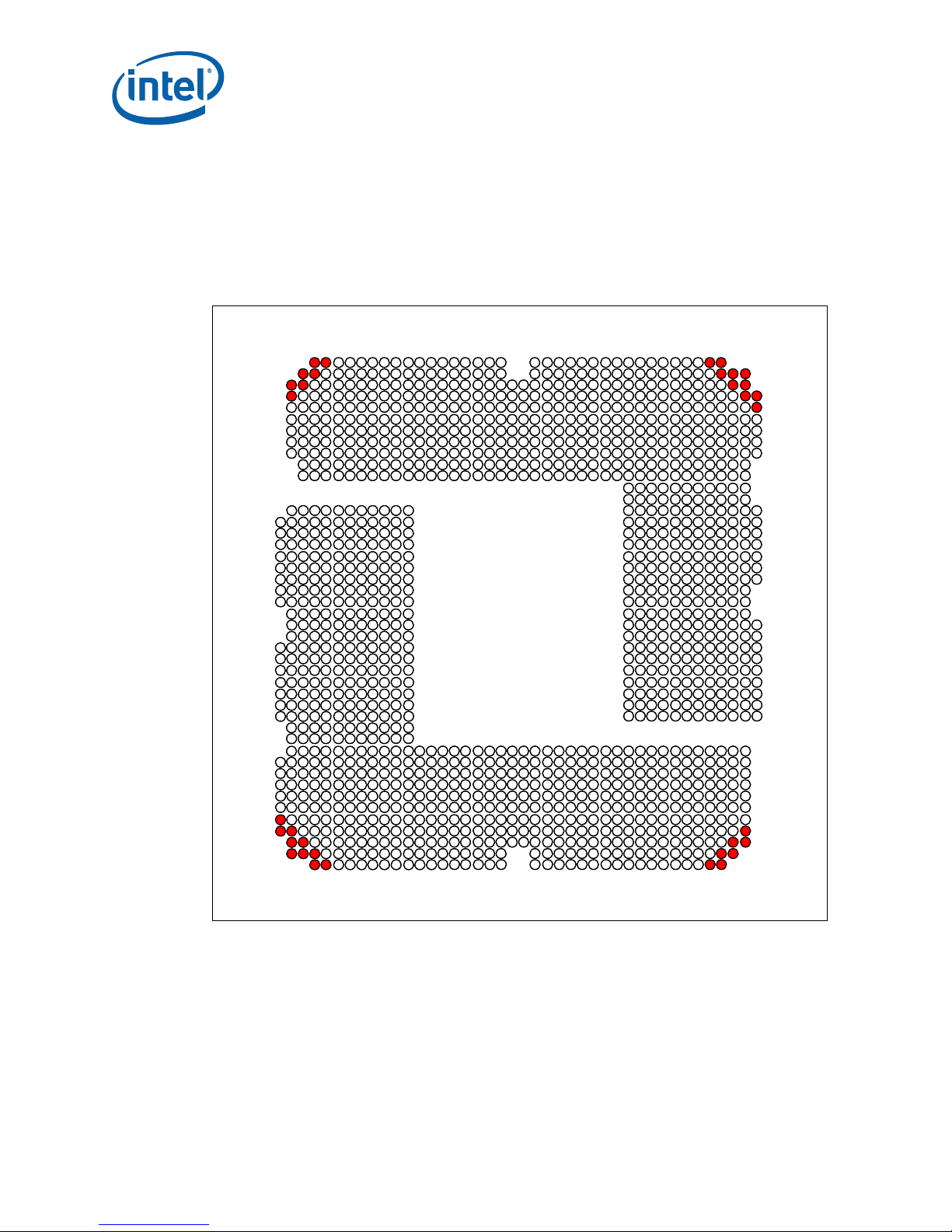
2-2 LGA1366 Socket Contact Numbering (Top View of Socket)............................................12
2-3 LGA1366 Socket Land Pattern (Top View of Board) ......................................................13
2-4 Attachment to Motherboard.................................................... ... .. ........................... ..14
2-5 Pick and Place Cover................................................................................................15
2-6 Package Installation / Removal Features .... ................................................................16
2-7 LGA1366 NCTF Solder Joints.....................................................................................18
3-1 ILM Cover Assembly................................................................................................20
3-2 ILM Assembly.........................................................................................................21
3-3 Pin1 and ILM Lever..................................................................................................22
4-1 Flow Chart of Knowledge-Based Reliability Evaluation Methodology ................................26
5-1 Comparison of Case Temperature vs. Sensor Based Specification...................................28
5-2 Thermal Profile ..................... .. ........................... ... .. ........................... .. .. .. ...............29
5-3 Thermal solution Performance...................................................................................30
5-4 Required YCA for various TAMBIENT Conditions...................................... .. ...................31
5-5 Thermal Solution Performance vs. Fan Speed..............................................................33
5-6 Fan Response Without TAMBIENT Data.......................................................................34
5-7 Fan Response with TAMBIENT Aware FSC...................................................................35
6-1 ATX Heatsink Reference Design Assembly...................................................................40
6-2 ATX KOZ 3-D Model Primary (Top) Side......................................................................41
6-3 RCBF5 Extrusion .....................................................................................................42
6-4 RCBF5 Clip.............................................................................................................43
6-5 Core......................................................................................................................44
6-6 Clip Core and Extrusion Assembly..............................................................................45
6-7 Critical Parameters for Interface to the Reference Clip..................................................45
6-8 Critical Core Dimensions ..........................................................................................46
B-1 Socket / Heatsink / ILM Keepout Zone Primary Side (Top)............................................52
B-2 Socket / Heatsink / ILM Keepout Zone Secondary Side (Bottom) ...................................53
B-3 Socket / Processor / ILM Keepout Zone Primary Side (Top)...........................................54
B-4 Socket / Processor / ILM Keepout Zone Secondary Side (Bottom)..................................55
B-5 Reference Design Heatsink Assembly (1 of 2)..............................................................56
4 Thermal and Mechanical Design Guide
Page 5

B-6 Reference Design Heatsink Assembly (2 of 2).............................................................57
B-7 Reference Fastener Sheet 1 of 4...............................................................................58
B-8 Reference Fastener Sheet 2 of 4...............................................................................59
B-9 Reference Fastener Sheet 3 of 4...............................................................................60
B-10 Reference Fastener Sheet 4 of 4 ...............................................................................61
B-11 Reference Clip - Sheet 1 of 2.......................................... ............................ .. ............62
B-12 Reference Clip - Sheet 2 of 2.......................................... ............................ .. ............63
C-1 Socket Mechanical Drawing (Sheet 1 of 4)..................................................................66
C-2 Socket Mechanical Drawing (Sheet 2 of 4)..................................................................67
C-3 Socket Mechanical Drawing (Sheet 3 of 4)..................................................................68
C-4 Socket Mechanical Drawing (Sheet 4 of 4)..................................................................69
D-1 Processor Installation Tool .......................................................................................72
Tables
1-1 Reference Documents.................................................................................................8
1-2 Terms and Descriptions ..............................................................................................8
4-1 Socket Component Mass................................ .. ............................ ........................... ..23
4-2 1366-land Package and LGA1366 Socket Stackup Height............................................... 23
4-3 Socket and ILM Mechanical Specifications....................................................................24
4-4 Electrical Requirements for LGA1366 Socket................................................................25
5-1 Thermal Solution Performance above TCONTROL..........................................................37
6-1 Processor Thermal Solution Requirements & Boundary Conditions...................................39
7-1 Use Conditions (Board Level).....................................................................................47
A-1 Reference Heatsink Enabled Components....................................................................49
A-2 LGA1366 Socket and ILM Components........................................................................49
A-3 Supplier Contact Information.....................................................................................49
B-1 Mechanical Drawing List............................................................................................51
C-1 Mechanical Drawing List............................................................................................65
Thermal and Mechanical Design Guide 5
Page 6
Revision History
Revision
Number
-001 • Initial release March 2009
Description Revision Date
§
6 Thermal and Mechanical Design Guide
Page 7
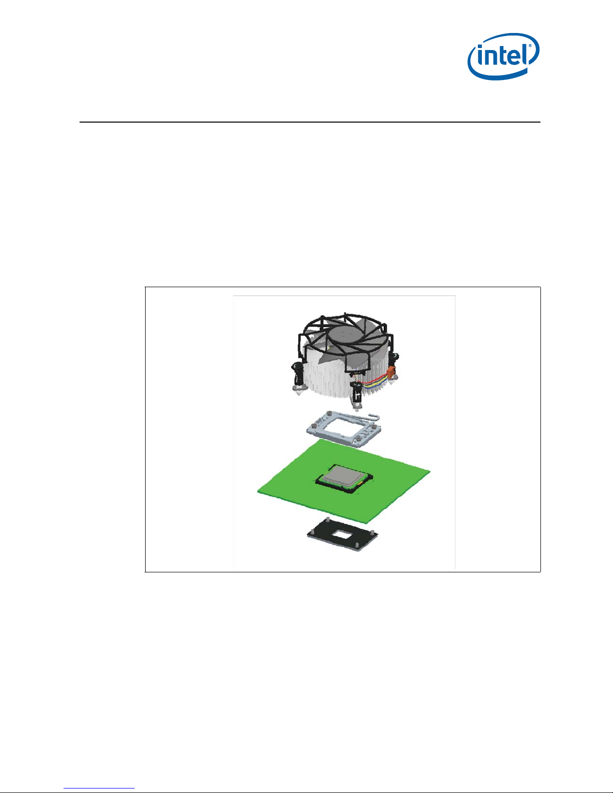
Introduction
1 Introduction
This document provides guidelines for the design of thermal and mechanical solutions
for the:
• Intel® X eon® Processor 3500 Series
Unless specifically required for clarity , this document will use “processor” in place of the
specific product names. The components described in this document include:
• The processor thermal solution (heatsink) and associated retention hardware.
• The LGA1366 socket and the Independent Loading Mechanism (ILM) and back
plate.
Figure 1-1. Processor Thermal Solution & LGA1366 Socket Stack
The goals of this document are:
• To assist board and system thermal mechanical designers.
• To assist designers and suppliers of processor heatsinks.
Thermal profiles and other processor specifications are provided in the appropriate
processor Datasheet.
Thermal/Mechanical Design Guide 7
Page 8
1.1 References
Material and concepts available in the following documents may be beneficial when
reading this document.
Table 1-1. Reference Documents
Document Location Notes
Intel® Xeon® Processor 3500 Series Processor Datasheet,
Volume 1
Intel® Xeon® Processor 3500 Series Processor Datasheet,
Volume 2
Intel® Xeon® Processor 3500 Series Processor Specification
Update
Notes:
1. Available electronically
1.2 Definition of Terms
Table 1-2. Terms and Descriptions (Sheet 1 of 2)
Term Description
Bypass Bypass is the area between a passive heatsink and any object that can act to form a
DTS Digital Thermal Sensor reports a relative die temperature as an offset from TCC
FSC Fan Speed Control
IHS Integrated Heat Spreader: a component of the processor package used to enhance the
ILM Independent Loading Mechanism provides the force needed to seat the 1366-LGA land
IOH Input Output Hub: a component of the chipset that provides I/O connections to PCIe,
LGA1366 socket The processor mates with the system board through this surface mount, 1366-contact
PECI The Platform Environment Control Interface (PECI) is a one- wire in terface that pro vides
Ψ
CA
Ψ
CS
Ψ
SA
T
CASE
T
CASE_MAX
TCC Thermal Control Circuit: Thermal monitor uses the TCC to reduce the die temperature
T
CONTROL
duct. For this example, it can be expressed as a dimension away from the outside
dimension of the fins to the nearest surface.
activation temperature.
thermal performance of the package. Component thermal solutions interface with the
processor at the IHS surface.
package onto the socket contacts.
drives and other peripherals
socket.
a communication channel between Intel processor and chipset components to external
monitoring devices.
Case-to-ambient thermal characterization parameter (psi). A measure of thermal
solution performance using t otal package power. Defined as (T
Package Power. Heat source should always be specified for Ψ measurements.
Case-to-sink thermal characterization parameter. A measure of thermal interface
material performance using total package po wer. Defined as (T
Package Power.
Sink-to-ambient thermal characterization parameter. A measure of heatsink thermal
performance using total package power. Defined as (T
The case temperature of the TTV measured at the geometric center of the topside of the
IHS.
The maximum case temperature as specified in a component specification.
by using clock modulation and/or operating frequency and input voltage adjustment
when the die temperature is very near its operating limits.
T
control.
is a static value below TCC activation used as a trigger point for fan speed
CONTROL
Introduction
321332 1
321344 1
321333 1
– TLA) / Total
CASE
– TS) / Total
CASE
– TLA) / Total Package Power.
S
8 Thermal/Mechanical Design Guide
Page 9
Introduction
Table 1-2. Terms and Descriptions (Sheet 2 of 2)
Term Description
TDP Thermal Design Power: Thermal solution should be designed to dissipate this target
Thermal Monitor A power reduction feature designed to decrease temperature after the processor has
Thermal Profile Line that defines case temperature specification of the TTV at a given power level.
TIM Thermal Interface Material: The thermally conductive compound between the heatsink
T
AMBIENT
T
SA
power level. TDP is not the maximum power that the processor can dissipate.
reached its maximum operating temperature.
and the processor case. This material fills the air gaps and voids, and enhances the
transfer of the heat from the processor case to the heatsink.
The measured ambient temperature locally surrounding the proces sor. The ambient
temperature should be measured just upstream of a p assive he atsink or at the fan inle t
for an active heatsink.
The system ambient air temperature external to a system chassis. This temperature is
usually measured at the chassis air inlets.
§
Thermal/Mechanical Design Guide 9
Page 10

Introduction
10 Thermal/Mechanical Design Guide
Page 11
LGA1366 Socket
2 LGA1366 Socket
This chapter describes a surface mount, LGA (Land Grid Array) socket intended for
Intel® Xeon® Processor 3500 Series. The socket provides I/O, power and ground
contacts. The socket contains 1366 contacts arrayed about a cavity in the center of the
socket with lead-free solder balls for surface mounting on the motherboard.
The socket has 1366 contacts with 1.016 mm X 1.016 mm pitch (X by Y) in a
43x41 grid array with 21x17 grid depopulation in the center of the array and selective
depopulation elsewhere.
The socket must be compatible with the package (processor) and the Independent
Loading Mechanism (ILM). The design includes a back plate which is integral to having
a uniform load on the socket solder joints. Socket loading specifications are listed in
Chapter 4.
Figure 2-1. LGA1366 Socket with Pick and Place Cover Removed
package socket
package
cavity
cavity
socket
Thermal/Mechanical Design Guide 11
Page 12
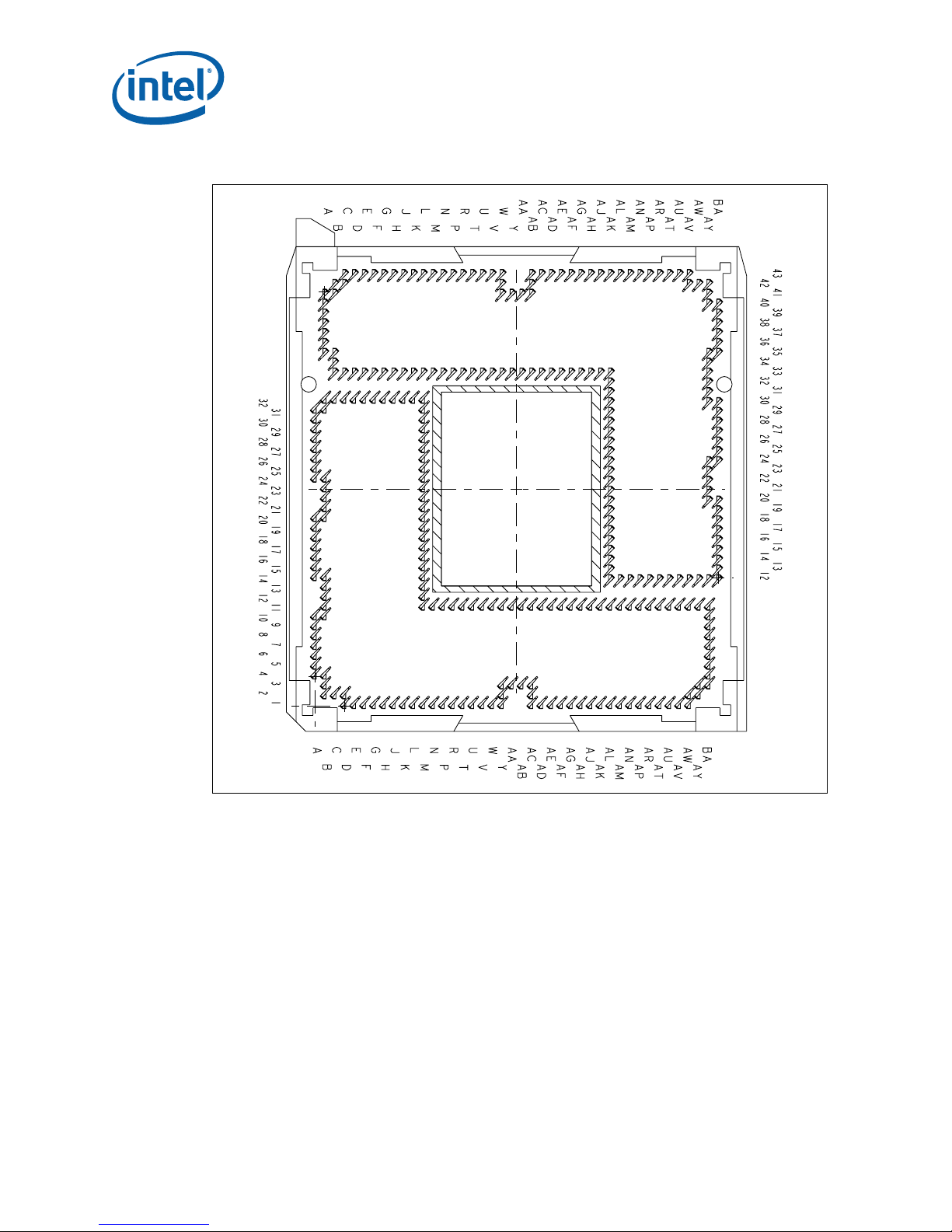
Figure 2-2. LGA1366 Socket Contact Numbering (Top View of Socket)
AP
AN
AM
AL
AK
AJ
AH
AG
AF
AE
AD
AC
AB
AA
Y
W
V
U
T
R
P
N
M
L
K
J
H
G
F
E
D
C
B
A
31 29 27 25 23 21 19 17 15 13 11 9 7 5
32 30 28 26 24 22 20 18 16 14 12 10 8 6 4
AR
AU
AT
LGA1366 Socket
BA
AY
AW
AV
43 41 39 37 35 33 31 29 27 25 23 21 19 17 15 13
42 40 38 36 34 32 30 28 26 24 22 20 18 16 14 12
BA
AY
AW
AV
AU
AT
AR
AP
AN
AM
AL
AK
AJ
AH
AG
AF
AE
AD
AC
AB
AA
Y
W
V
U
T
R
P
N
M
L
K
J
H
G
F
E
D
C
B
A
12 Thermal/Mechanical Design Guide
Page 13
LGA1366 Socket
2.1 Board Layout
The land pattern for the LGA1366 socket is 40 mils X 40 mils (X by Y), and the pad size
is 18 mils. Note that there is no round-off (conversion) error between socket pitch
(1.016 mm) and board pitch (40 mil) as these values are equivalent.
Figure 2-3. LGA1366 Socket Land Pattern (Top View of Board)
A C E G J L N R U W AA AC AE AG AJ AL AN AR AU AW BA
B D F H K M P T V Y AB AD AF AH AK AM AP AT AV AY
32
32
31
31
30
30
29
29
28
28
27
27
26
26
25
25
24
24
23
23
22
22
21
21
20
20
19
19
18
18
17
17
16
16
15
15
14
14
13
13
12
12
11
11
10
10
9
9
8
8
7
7
6
6
5
5
4
4
3
3
2
2
1
1
A C E G J L N R U W AA AC AE AG AJ AL AN AR AU AW BA
B D F H K M P T V Y AB AD AF AH AK AM AP AT AV AY
43
42
41
40
39
38
37
36
35
34
33
32
31
30
29
28
27
26
25
24
23
22
21
20
19
18
17
16
15
14
13
12
Thermal/Mechanical Design Guide 13
Page 14
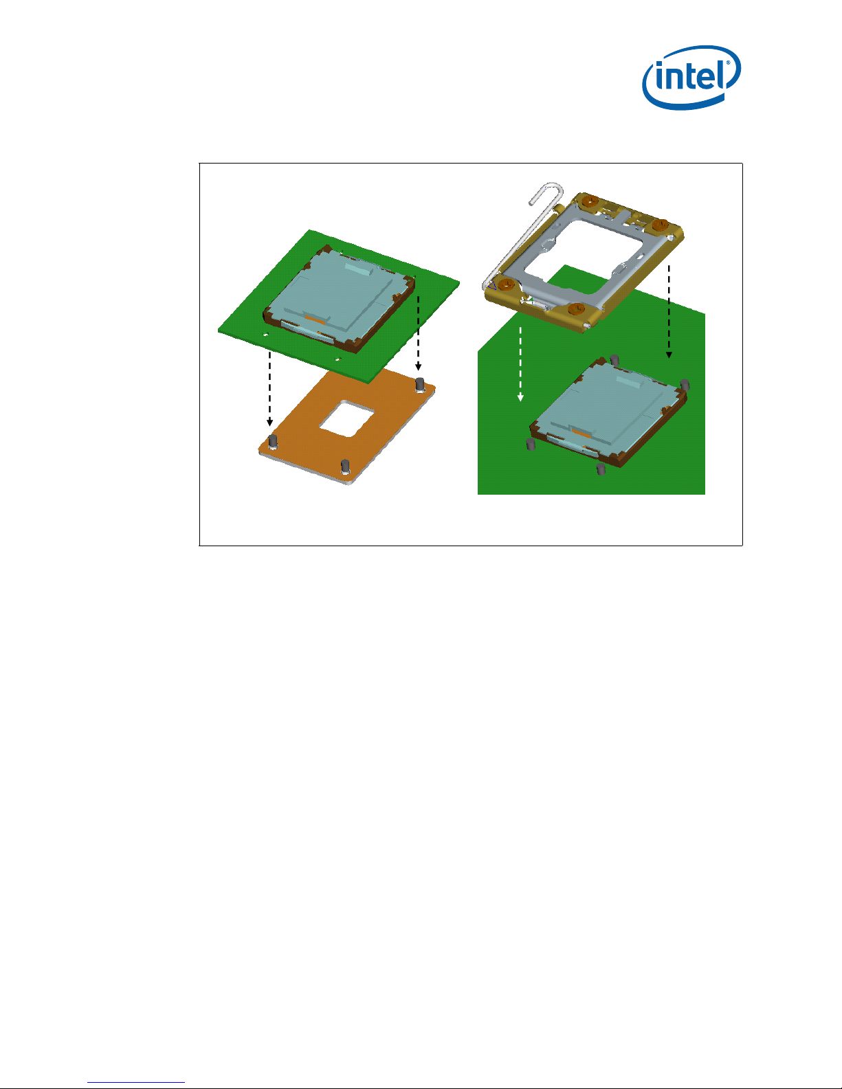
2.2 Attachment to Motherboard
The socket is attached to the motherboard by 1366 solder balls. There are no additional
external methods (that is, screw, extra solder, adhesive, and so on) to attach the
socket.
As indicated in Figure 2-4, the Independent Loading Mechanism (ILM) is not present
during the attach (reflow) process.
Figure 2-4. Attachment to Motherboard
LGA1366 Socket
ILM
LGA 1366 Socket
2.3 Socket Components
The socket has two main components, the socket body and Pick and Place (PnP) cover,
and is delivered as a single integral assembly. Refer to Appendix C for detailed
drawings.
2.3.1 Socket Body Housing
The housing material is thermoplastic or equivalent with UL 94 V -0 flame rating capable
of withstanding 260 °C for 40 seconds (typical reflow/rework). The socket coefficient of
thermal expansion (in the XY plane), and creep properties, must be such that the
integrity of the socket is maintained for the conditions listed in Chapter 7.
The color of the housing will be dark as compared to the solder balls to provide the
contrast needed for pick and place vision systems.
2.3.2 Solder Balls
A total of 1366 solder balls corresponding to the contacts are on the bottom of the
socket for surface mounting with the motherboard.
The socket has the following solder ball material:
• Lead free SAC (SnAgCu) solder alloy with a silver (Ag) content between 3% and
4% and a melting temperature of approximately 217 °C. The alloy must be
compatible with immersion silver (ImAg) motherboard surface finish and a SAC
alloy solder paste.
The co-planarity (profile) and true position requirements are defined in Appendix C.
14 Thermal/Mechanical Design Guide
Page 15
LGA1366 Socket
2.3.3 Contacts
Base material for the contacts is high strength copper alloy.
For the area on socket contacts where processor lands will mate, there is a 0.381 μm
[15 μinches] minimum gold plating over 1.27 μm [50 μinches] minimum nickel
underplate.
No contamination by solder in the contact area is allowed during solder reflow.
2.3.4 Pick and Place Cover
The cover provides a planar surface for vacuum pick up used to place components in
the Surface Mount Technology (SMT) manufacturing line. The cover remains on the
socket during reflow to help prevent contamination during reflow. The cover can
withstand 260 °C for 40 seconds (typical reflow/rework profile) and the conditions
listed in Chapter 7 without degrading.
As indicated in Figure 2-5, the cover remains on the socket during ILM installation, and
should remain on whenever possible to help prevent damage to the socket contacts.
Cover retention must be sufficient to support the socket weight during lifting,
translation, and placement (board manufacturing), and during board and system
shipping and handling.
The covers are designed to be interchangeable between socket suppliers. As indicated
in Figure 2-5, a Pin1 indicator on the cover provides a visual reference for proper
orientation with the socket.
Figure 2-5. Pick and Place Cover
ILM
Installation
Pin 1 Pin 1
Pick and
Place Cover
Thermal/Mechanical Design Guide 15
Page 16
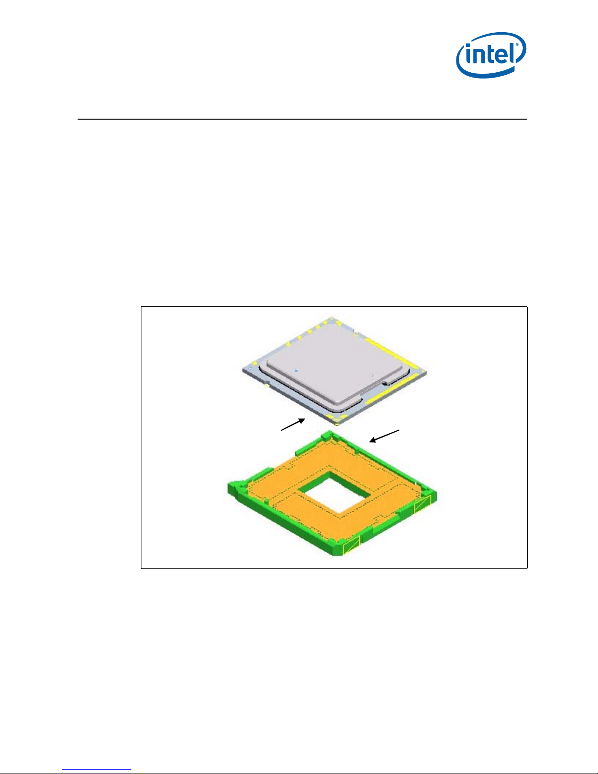
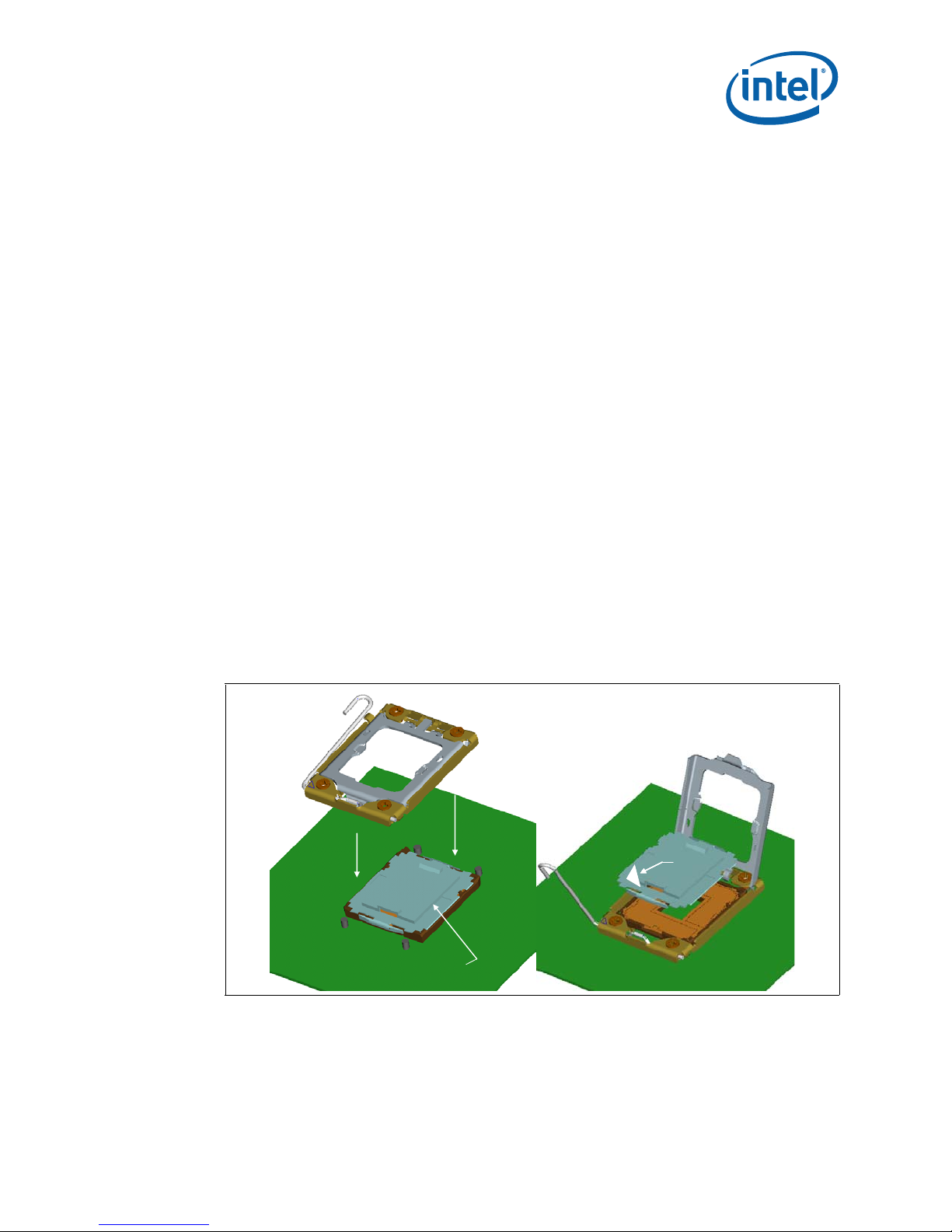
2.4 Package Installation / Removal
As indicated in Figure 2-6, access is provided to facilitate manual installation and
removal of the package.
To assist in package orientation and alignment with the socket:
• The package Pin1 triangle and the socket Pin1 chamfer provide visual reference for
proper orientation.
• The package substrate has orientation notches along two opposing edges of the
package, offset from the centerline. The socket has two corresponding orientation
posts to physically prevent mis-orientation of the package. These orientation
features also provide initial rough alignment of package to socket.
• The socket has alignment walls at the four corners to provide final alignment of the
package.
See Appendix D for information regarding a tool designed to provide mechanical
.
Figure 2-6. Package Installation / Removal Features
assistance during processor installation and removal.
LGA1366 Socket
orientation
orientation
notch
notch
alignment
Pin1 triangle
Pin1 triangle
access
access
orientation
orientation
post
post
Pin1 chamfer
Pin1 chamfer
alignment
walls
walls
2.4.1 Socket Standoffs and Package Seating Plane
Standoffs on the bottom of the socket base establish the minimum socket height after
solder reflow and are specified in Appendix C.
Similarly, a seating plane on the topside of the socket establishes the minimum
package height. See Section 4.2 for the calculated IHS height above the motherboard.
16 Thermal/Mechanical Design Guide
Page 17

LGA1366 Socket
2.5 Durability
The socket must withstand 30 cycles of processor insertion and removal. The max
chain contact resistance from Table 4-4 must be met when mated in the 1st and 30th
cycles.
The socket Pick and Place cover must withstand 15 cycles of insertion and removal.
2.6 Markings
There are three markings on the socket:
• LGA1366: Font type is Helvetica Bold - minimum 6 point (2.125 mm).
• Manufacturer's insignia (font size at supplier's discretion).
• Lot identification code (allows traceability of manufacturing date and location).
All markings must withstand 260 °C for 40 seconds (typical reflow/rework profile)
without degrading, and must be visible after the socket is mounted on the
motherboard.
LGA1366 and the manufacturer's insignia are molded or laser marked on the side wall.
2.7 Component Insertion Forces
Any actuation must meet or exceed SEMI S8-95 Safety Guidelines for Ergonomics/
Human Factors Engineering of Semiconductor Manu facturing Equipment, example Table
R2-7 (Maximum Grip Forces). The socket must be designed so that it requires no force
to insert the package into the socket.
2.8 Socket Size
Socket information needed for motherboard design is given in Appendix C.
This information should be used in conjunction with the reference motherboard keep-
out drawings provided in Appendix B to ensure compatibility with the reference thermal
mechanical components.
Thermal/Mechanical Design Guide 17
Page 18
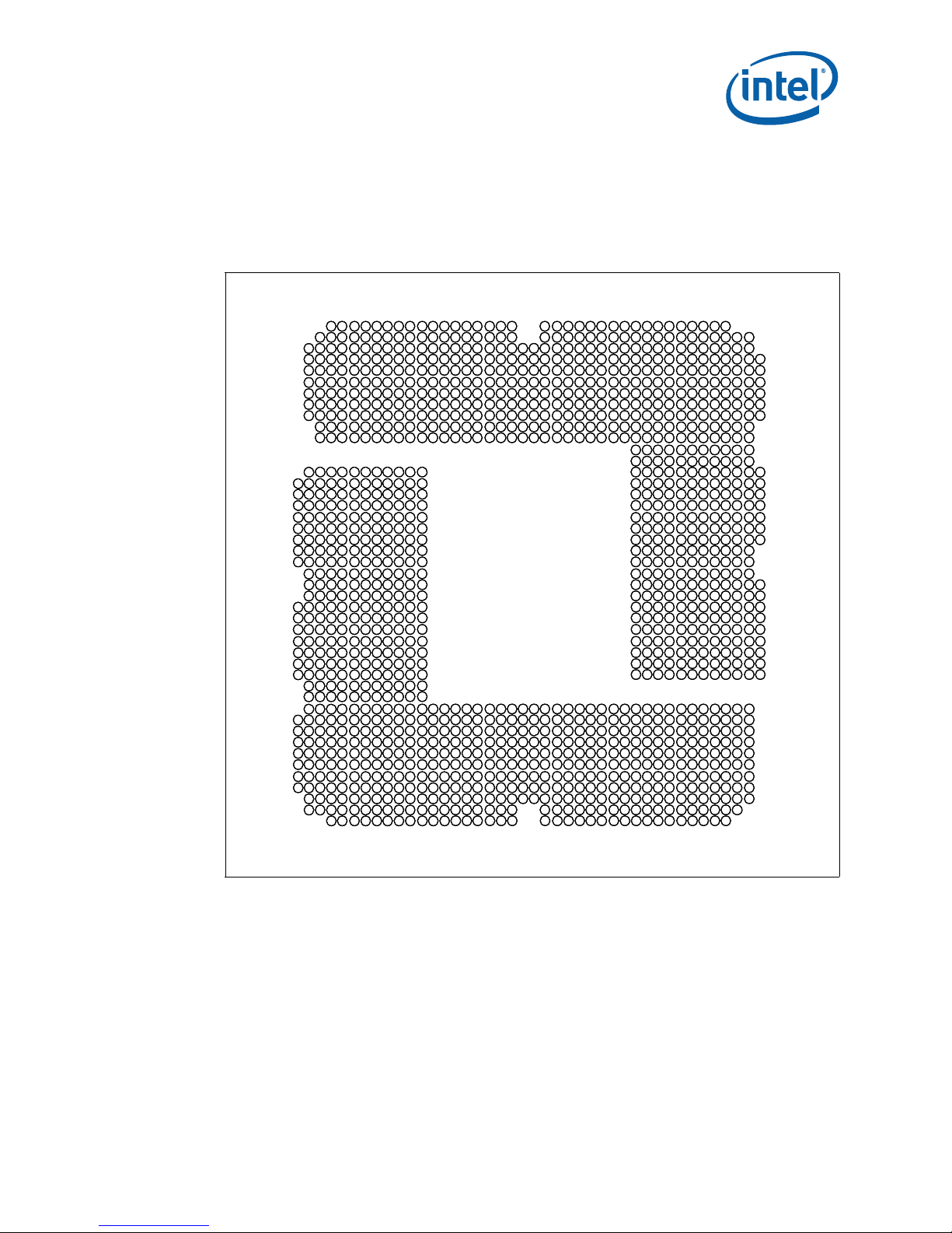
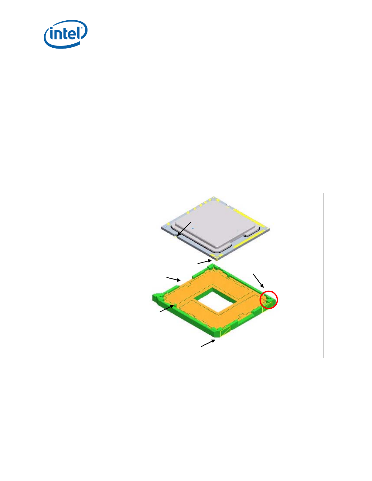
2.9 LGA1366 Socket NCTF Solder Joints
Intel has defined selected solder joints of the socket as non-critical to function (NCTF)
for post environmental testing. The processor signals at NCTF locations are typically
redundant ground or non-critical reserved, so the loss of the solder joint continuity at
end of life conditions will not affect the overall product functionality. Figure 2-7
.
Figure 2-7. LGA1366 NCTF Solder Joints
identifies the NCTF solder joints.
A C E G J L N R U W AA AC AE AG AJ AL AN AR AU AW BA
B D F H K M P T V Y AB AD AF AH AK AM AP AT AV AY
32
32
31
31
30
30
29
29
28
28
27
27
26
26
25
25
24
24
23
23
22
22
21
21
20
20
19
19
18
18
17
17
16
16
15
15
14
14
13
13
12
12
11
11
10
10
9
9
8
8
7
7
6
6
5
5
4
4
3
3
2
2
1
1
A C E G J L N R U W AA AC AE AG AJ AL AN AR AU AW BA
B D F H K M P T V Y AB AD AF AH AK AM AP AT AV AY
LGA1366 Socket
43
42
41
40
39
38
37
36
35
34
33
32
31
30
29
28
27
26
25
24
23
22
21
20
19
18
17
16
15
14
13
12
18 Thermal/Mechanical Design Guide
§
Page 19

Independent Loading Mechanism (ILM)
3 Independent Loading
Mechanism (ILM)
The Independent Loading Mechanism (ILM) provides the force needed to seat the
1366-LGA land package onto the socket contacts. The ILM is physically separate from
the socket body. The assembly of the ILM to the board is expected to occur after wave
solder. The exact assembly location is dependent on manufacturing preference and test
flow.
Note: The ILM has two critical functions: deliver the force to seat the processor onto the
socket contacts and distribute the resulting compressive load evenly through the socket
solder joints.
Note: The mechanical design of the ILM is integral to the overall functionality of the LGA1366
socket. Intel performs detailed studies on integration of processor package, socket and
ILM as a system. These studies directly impact the design of the ILM. The Intel
reference ILM will be “build to print” from Intel controlled drawings. Intel recommends
using the Intel Reference ILM. Custom non-Intel ILM designs do not benefit from Intel's
detailed studies and may not incorporate critical design parameters.
3.1 Design Concept
The ILM consists of two assemblies that will be procured as a set from the enabled
vendors. These two components are ILM cover assembly and back plate.
3.1.1 ILM Cover Assembly Design Overview
The ILM Cover assembly consists of four major pieces: load lever, load plate, frame and
the captive fasteners.
The load lever and load plate are stainless steel. The frame and fasteners are high
carbon steel with appropriate plating. The fasteners are fabricated from a high carbon
steel. The frame provides the hinge locations for the load lever and load plate.
The cover assembly design ensures that once assembled to the back plate and the load
lever is closed, the only features touching the board are the captive fasteners. The
nominal gap of the frame to the board is ~1 mm when the load plate is closed on the
empty socket or when closed on the processor package.
When closed, the load plate applies two point loads onto the IHS at the “dimpled”
features shown in Figure 3-1. The reaction force from closing the load plate is
transmitted to the frame and through the captive fasteners to the back plate. Some of
the load is passed through the socket body to the board inducing a slight compression
on the solder joints.
Thermal/Mechanical Design Guide 19
Page 20

Figure 3-1. ILM Cover Assembly
Load Lever
Load Lever
Load Plate
Load Plate
Independent Loading Mechanism (IL M )
Captive Fastener (4x)
Captive Fastener (4x)
Frame
Frame
3.1.2 ILM Back Plate Design Overview
The back plate for single processor workstation products consists of a flat steel back
plate with threaded studs for ILM attach. The threaded studs have a smooth surface
feature that provides alignment for the back plate to the motherboard for proper
assembly of the ILM around the socket. A clearance hole is located at the center of the
plate to allow access to test points and backside capacitors. An insulator is pre-applied.
3.2 Assembly of ILM to a Motherboard
The ILM design allows a bottoms up assembly of the components to the board. In
step 1, (see Figure 3-2), the back plate is placed in a fixture. Holes in the motherboard
provide alignment to the threaded studs. In step 2, the ILM cover assembly is placed
over the socket and threaded studs. Using a T20 Torx* driver fasten the ILM cover
assembly to the back plate with the four captive fasteners. Torque to 8 ± 2 inchpounds. The length of the threaded studs accommodate board thicknesses from
0.062” to 0.100”.
20 Thermal/Mechanical Design Guide
Page 21
Independent Loading Mechanism (ILM)
.
Figure 3-2. ILM Assembly
Socket Body Reflowed on board
Socket Body Reflowed on board
Socket Body with Back Plate on board
Socket Body with Back Plate on board
Step 1 Step 2
Step 1 Step 2
Thermal/Mechanical Design Guide 21
Page 22
As indicated in Figure 3-3, socket protrusion and ILM key features prevent 180-degree
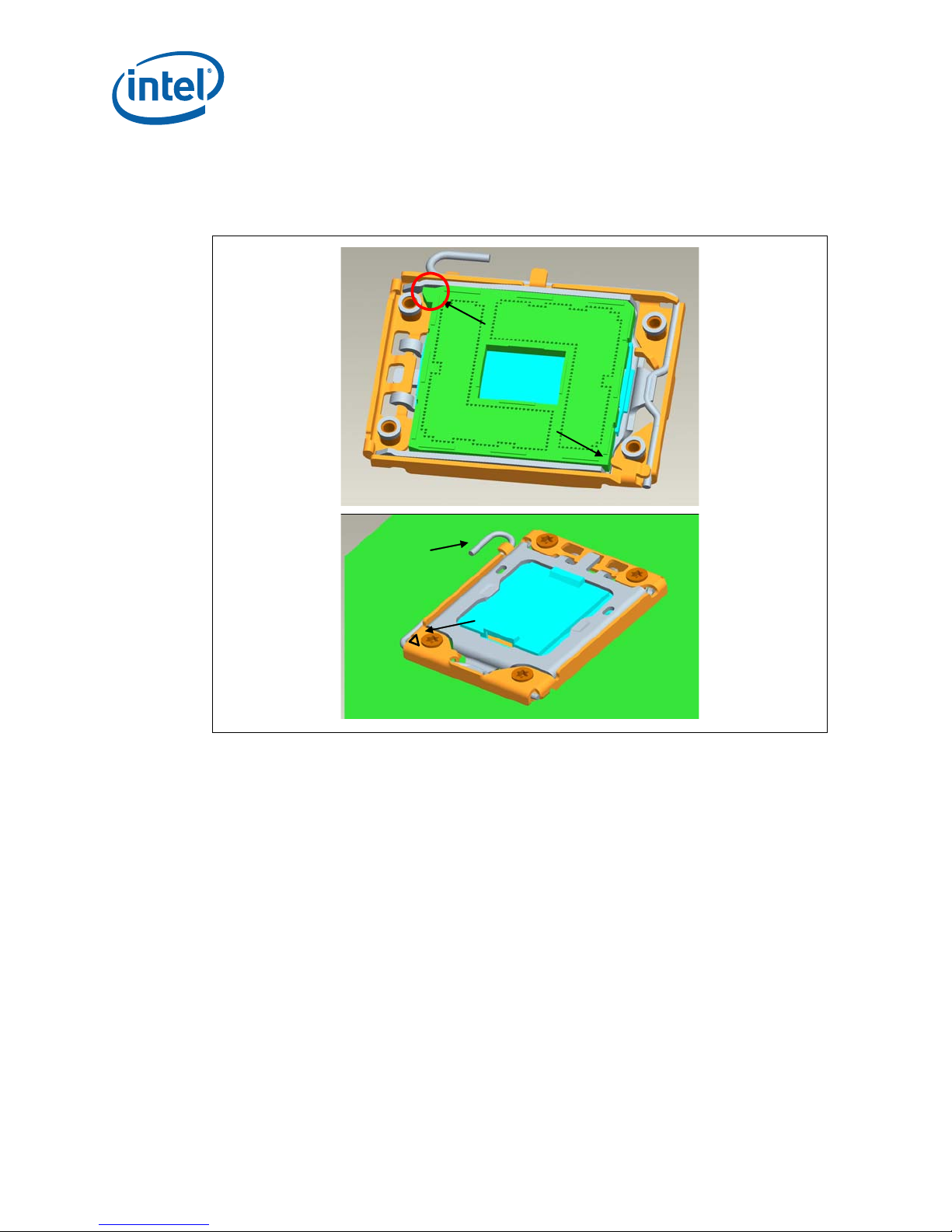
rotation of ILM cover assembly with respect to the socket. The result is a specific Pin 1
orientation with respect to the ILM lever.
Figure 3-3. Pin1 and ILM Lever
Independent Loading Mechanism (IL M )
Protrusion
ILM Key
ILM
Lever
Pin 1
§
22 Thermal/Mechanical Design Guide
Page 23

LGA1366 Socket and ILM Electrical, Mechanical, and Environmental Specifications
4 LGA1366 Socket and ILM
Electrical, Mechanical, and
Environmental Specifications
This chapter describes the electrical, mechanical, and environmental specifications for
the LGA1366 socket and the Independent Loading Mechanism.
4.1 Component Mass
Table 4-1. Socket Component Mass
Component Mass
Socket Body, Contacts and PnP Cover 15 g
ILM Cover 43 g
ILM Back Plate 51 g
4.2 Package/Socket Stackup Height
Table 4-2 provides the stackup height of a processor in the 1366-land LGA package and
LGA1366 socket with the ILM closed and the processor fully seated in the socket.
Table 4-2. 1366-land Package and LGA1366 Socket Stackup Height
Integrated Stackup Height (mm)
From Top of Board to Top of IHS
Notes:
1. This data is provided for information only, and should be derived from: (a) the height of the s ocke t seating
plane above the motherboard after reflow, given in Appendix C, (b) the height of the package, from the
package seating plane to the top of the IHS, and accounting for its nominal variation and tolerances that
are given in the corresponding processor datasheet.
2. This value is a RSS calculation.
7.729 ± 0.282 mm
4.3 Socket Maximum Temperature
The power dissipated within the socket is a function of the current at the pin level and
the effective pin resistance. To ensure socket long term reliability, Intel defines socket
maximum temperature using a via on the underside of the motherboard. Exceeding the
temperature guidance may result in socket body deformation, or increases in thermal
and electrical resistance which can cause a thermal runaway and eventual electrical
failure. The guidance for socket maximum temperature is listed below:
• Via temperature under socket < 96 °C
Thermal/Mechanical Design Guide 23
Page 24

LGA1366 Socket and ILM Electrical, Mechanical, and Environmental Specifications
4.4 Loading Specifications
The socket will be tested against the conditions listed in Chapter 7 with heatsink and
the ILM attached, under the loading conditions outlined in this chapter.
Table 4-3 provides load specifications for the LGA1366 socket with the ILM installed.
The maximum limits should not be exceeded during heatsink assembly, shipping
conditions, or standard use condition. Exceeding these limits during test may result in
component failure. The socket body should not be used as a mechanical reference or
load-bearing surface for thermal solutions.
Table 4-3. Socket and ILM Mechanical Specifications
Parameter Min Max Notes
Static compressive load from ILM cover to
processor IHS
Heatsink Static Compressive Load 0 N [0 lbf] 266 N [60 lbf] 1, 2, 3
Total Static Compressive Load
(ILM plus Heatsink)
Dynamic Compressive Load
(with heatsink installed)
Pick and Place Cover Insertion / Removal force N/A 10.2 N [2.3 lbf]
Load Lever actuation force N/A 38.3 N [8.6 lbf] in the
470 N [106 lbf] 623 N [140 lbf] 3, 4, 7
470 N (106 lbf) 890 N (200 lbf) 3, 4
N/A 890 N [200 lbf] 1, 3, 5, 6
vertical direction
10.2 N [2.3 lbf] in the
lateral direction.
Notes:
1. These specifications apply to uniform compressive loading in a direction perpendicular to the IHS top
surface.
2. This is the minimum and maximum static force that can be applied by the heatsink and it’s retention
solution to maintain the heatsink to IHS interface. This does not imply the Intel reference TIM is validated
to these limits.
3. Loading limits are for the LGA1366 socket.
4. This minimum limit defines the compres sive forc e require d to electrically seat the processor onto the sock et
contacts.
5. Dynamic loading is defined as an 11 ms duration average load superimposed on the static load
requirement.
6. Test condition used a heatsink mass of 550 gm [1.21 lb] with 50 g acceler ation measured at h eatsink mass.
The dynamic portion of this specification in the product application can have flexibility in specific values, but
the ultimate product of mass times acceleration should not exceed this dynamic load.
7. Conditions must be satisfied at the beginning of life and the loading system stiffness for non-reference
designs need to meet a specific stiffness range to satisfy end of life loading requirements.
4.5 Electrical Requirements
LGA1366 socket electrical requirements are measured from the socket-seating plane of
the processor to the component side of the socket PCB to which it is attached. All
specifications are maximum values (unless otherwise stated) for a single socket
contact, but includes effects of adjacent contacts where indicated.
24 Thermal/Mechanical Design Guide
Page 25

LGA1366 Socket and ILM Electrical, Mechanical, and Environmental Specifications
Table 4-4. Electrical Requirements for LGA1366 Socket
Parameter Value Comment
Mated loop inductance, Loop
Mated partial mutual inductance, L
Maximum mutual capacitance, C.
Socket Average Contact R esistance
(EOL)
Max Individual Contact Resistance
(EOL)
Bulk Resistance Increase
Dielectric Withstand Voltage
Insulation Resistance
<3.9nH
NA
<1 pF
15.2 mΩ
≤ 100 mΩ
≤ 3 mΩ
360 Volts RMS
800 MΩ
The inductance calculated for two contacts,
considering one forward conductor an d one return
conductor. These values must be satisfied at the
worst-case height of the socket.
The inductance on a contact due to any single
neighboring contact.
The capacitance between two contacts
The socket average contact resistance target is
derived from average of every chain contact
resistance for each part used in testing, with a
chain contact resistance defined as the resistance
of each chain minus resistance of shorting bars
divided by number of lands in the daisy chain.
The specification listed is at room temperature
and has to be satisfied at all time.
Socket Contact Resistance: The resistance of
the socket contact, solderball, and interface
resistance to the interposer land.
The specification listed is at room temperature
and has to be satisfied at all time.
Socket Contact Resistance: The resistance of
the socket contact, solderball, and interface
resistance to the interposer land; gaps included.
The bulk resistance increase per contact from
24 °C to 107 °C
4.6 Environmental Requirements
Design, including materials, shall be consistent with the manufacture of units that meet
the following environmental reference points.
The reliability targets in this chapter are based on the expected field use environment
for these products. The test sequence for new sockets will be developed using the
knowledge-based reliability evaluation methodology, which is acceleration factor
dependent. A simplified process flow of this methodology can be seen in Figure 4-1.
Thermal/Mechanical Design Guide 25
Page 26

LGA1366 Socket and ILM Electrical, Mechanical, and Environmental Specifications
Figure 4-1. Flow Chart of Knowledge-Based Reliability Evaluation Methodology
Establish the
market/expected use
environment for the
technology
Develop Speculative
stress conditions based on
historical data, content
experts, and literature
search
Freeze stressing
requirements and perform
additional data turns
Perform stressing to
validate accelerated
stressing assumptions and
determine acceleration
factors
A detailed description of this methodology can be found at:
ftp://download.intel.com/technology/itj/q32000/pdf/reliability.pdf.
§
26 Thermal/Mechanical Design Guide
Page 27

Sensor Based Thermal Specification Design Guidance
5 Sensor Based Thermal
Specification Design Guidance
The introduction of the sensor based thermal specification presents opportunities for
the system designer to optimize the acoustics and simplify thermal validation. The
sensor based specification utilizes the Digital Thermal Sensor information accessed
using the PECI interface.
This chapter will review thermal solution design options, fan speed control design
guidance & implementation options and suggestions on validation both with the TTV
and the live die in a shipping system.
5.1 Sensor Based Specification Overview
Create a thermal specification that meets the following requirements:
• Use Digital Thermal Sensor (DTS) for real-time thermal specification compliance.
• Single point of reference for thermal specification compliance over all operating
conditions.
• Does not required measuring processor power & case temperature during
functional system thermal validation.
• Opportunity for acoustic benefits for DTS values between T
CONTROL
and -1.
The current specification based on the processor case temperature has some notable
gaps to optimal acoustic design. When the ambient temperature is less than the
maximum design point, the fan speed control system (FSC) will over cool the processor.
The FSC has no feedback mechanism to detect this over cooling. This is shown in the
top half of Figure 5-1.
The sensor based specification will allow the FSC to be operated at the maximum
allowable silicon temperature or T
acoustics for operation above T
for the measured ambient. This will provide optimal
J
CONTROL
. See lower half of Figure 5-1.
Thermal/Mechanical Design Guide 27
Page 28

Sensor Based Thermal Specification Design Guidance
Figure 5-1. Comparison of Case Temperature vs. Sensor Based Specification
Ta = 43.2 C
Ta = 43.2 C
Tcontrol
Tcontrol
Ta = 30 C
Ta = 30 C
Ψ-ca = 0.292
Ψ-ca = 0.292
TDP
Power
Power
Current Sp ecification (Case Temp)
Current Sp ecification (Case Temp)
Ψ-ca = 0.362
Ψ-ca = 0.362
Tcontrol
Tcontrol
Ta = 30 C
Ta = 30 C
TDP
Ψ-ca = 0.292
Ψ-ca = 0.292
TDP
Power
Power
Sensor Based Specification (DTS Temp)
Sensor Based Specification (DTS Temp)
TDP
5.2 Sensor Based Thermal Specification
The sensor based thermal specification consists of two parts. The first is a thermal
profile that defines the maximum TTV T
thermal profile defines the boundary conditions for validation of the thermal solution.
The second part is a defined thermal solution performance (Ψ
DTS value as reported over the PECI bus when DTS is greater than T
defines the operational limits for the processor using the TTV validated thermal
solution.
5.2.1 TTV Thermal Profile
For the sensor based specification the only reference made to a case temperature
measurement is on the TTV. Functional thermal validation will not require the user to
apply a thermocouple to the processor package or measure processor power.
Note: All functional compliance testing will be based on fan speed response to the reported
DTS values above T
will be necessary.
CONTROL
. As a result no conversion of TTV T
as a function of TTV power dissipation. The
CASE
) as a function of the
CA
CONTROL
to processor T
CASE
. This
CASE
28 Thermal/Mechanical Design Guide
Page 29

Sensor Based Thermal Specification Design Guidance
As in previous product specifications, a knowledge of the system boundary conditions is
necessary to perform the heatsink validation. Section 5.3.1 will provide more detail on
defining the boundary conditions. The TTV is placed in the socket and powered to the
recommended value to simulate the TDP condition. See Figure 5-2 for an example of
the processor TTV thermal profile.
Figure 5-2. Thermal Profile
70.0
65.0
60.0
55.0
TTV Tcase in C
50.0
45.0
40.0
0 102030405060708090100110120130
y = 43. 2 + 0. 19 * P
TTV Power (W)
Note: This graph is provided as a reference. Please refer to the appropriate processor
datasheet for the specification.
5.2.2 Specification When DTS value is Greater than T
The product specification provides a table of ΨCA values at DTS = T
DTS = -1 as a function of T
AMBIENT
(inlet to heatsink). Between these two defined
CONTROL
CONTROL
and
points, a linear interpolation can be done for any DTS value reported by the processor.
A copy of the specification is provided as a reference in Table 5-1 of Section 5.6.
The fan speed control algorithm has enough information using only the DTS value and
T
AMBIENT
to command the thermal solution to provide just enough cooling to keep the
part on the thermal profile.
As an example, the data in Table 5-1 has been plotted in Figure 5-3 to show the
required Ψ
required Ψ
at 25, 30, 35, and 39 °C T
CA
which means lower fan speeds and reduced acoustics from the processor
CA
thermal solution.
In the prior thermal specifications this region, DTS values greater than T
defined by the processor thermal profile. This required the user to estimate the
processor power and case temperature. Neither of these two data points are accessible
in real time for the fan speed control system. As a result, the designer had to assume
the worst case T
Thermal/Mechanical Design Guide 29
AMBIENT
AMBIENT
. The lower the ambient, the higher the
CONTROL
, was
and drive the fans to accommodate that boundary condition.
Page 30

Figure 5-3. Thermal solution Performance
Sensor Based Thermal Specification Design Guidance
5.3 Thermal Solution Design Process
Thermal solution design guidance for this specification is the same as with previous
products. The initial design must take into account the target market and overall
product requirements for the system. This can be broken down into several steps:
• Boundary condition definition
• Thermal design / modelling
•Thermal testing
5.3.1 Boundary Condition Definition
Using the knowledge of the system boundary conditions (e.g., inlet air temperature,
acoustic requirements, cost, design for manufacturing, package and socket mechanical
specifications and chassis environmental test limits) the designer can make informed
thermal solution design decisions.
The thermal boundary conditions for an ATX tower system are as follows:
•T
EXTERNAL
•T
RISE
•T
AMBIENT
Based on the system boundary conditions, the designer can select a T
to use in thermal modelling. The assumption of a T
the required Ψ
assumed T
Figure 5-4 shows a number of satisfactory solutions for the processor.
= 35 °C. This is typical of a maximum system operating environment
= 4 °C. This is typical of a chassis compliant to CAG 1.1
= 39 °C (T
needed to meet TTV T
CA
AMBIENT
AMBIENT
can utilize a design with a higher ΨCA, which can have a lower cost.
= T
EXTERNAL
CASEMAX
+ T
RISE
)
AMBIENT
at TDP. A system that can deliver lower
AMBIENT
and ΨCA
has a significant impact on
30 Thermal/Mechanical Design Guide
Page 31

Sensor Based Thermal Specification Design Guidance
Note: If the assumed T
thermal solution performance may not be sufficient to meet the product requirements.
The results may be excessive noise from fans having to operate at a speed higher than
intended. In the worst case this can lead to performance loss with excessive activation
of the Thermal Control Circuit (TCC).
Figure 5-4. Required Ψ
for various T
CA
AMBIENT
is inappropriate for the intended system environment, the
AMBIENT
Conditions
Note: If an ambient of greater than 43.2 °C is necessary based on the boundary conditions a
thermal solution with a Ψ
lower than 0.19 °C/W will be required.
CA
5.3.2 Thermal Design and Modelling
Based on the boundary conditions the designer can now make the design selection of
the thermal solution components. The major components that can be mixed are the
fan, fin geometry , heat pipe or air cooled solid core design. There are cost and acoustic
trade-offs the customer must make.
To aide in the design process Intel provides TTV thermal models. Please consult your
Intel Field Sales Engineer for these tools.
Thermal/Mechanical Design Guide 31
Page 32

Sensor Based Thermal Specification Design Guidance
5.3.3 Thermal Solution Validation
5.3.3.1 Test for Compliance to the TTV Therm al Profile
This step is the same as previously suggested for prior products. The thermal solution
is mounted on a test fixture with the TTV and tested at the following conditions:
• TTV is powered to the TDP condition
• Thermal solution fan operating at full speed
•T
AMBIENT
at the boundary condition from Section 5.3.1
The following data is collected: TTV power, TTV T
CASE
, and T
AMBIENT
, and used to
calculate ΨCA, which is defined as:
Ψ
= (TTV T
CA
CASE
– T
AMBIENT
) / Power
This testing is best conducted on a bench to eliminate as many variables as possible
when assessing the thermal solution performance. The boundary condition analysis as
described in Section 5.3.1 should help in making the bench test simpler to perform.
5.3.3.2 Thermal Solution Characterization for Fan Speed Control
The final step in thermal solution validation is to establish the thermal solution
performance,ΨCA and acoustics as a function of fan speed. This data is necessary to
allow the fan speed control algorithm developer to program the device. It also is
needed to asses the expected acoustic impact of the processor thermal solution in the
system.
The characterization data should be taken over the operating range of the fan. Using
the RCHF5 as the example the fan is operational from 600 to 3500 RPM. The data was
collected at several points and a curve was fit to the data see Figure 5-5. Taking data at
6 evenly distributed fan speeds over the operating range should provide enough data to
establish a 3-variable equation. By using the equation from the curve fitting a complete
set of required fan speeds as a function of Ψ
reference thermal solution characterization are provided in Table 5-1.
The fan speed control device may modulate the thermal solution fan speed (RPM) by
one of two methods a pulse width modulation (PWM) signal or varying the voltage to
the fan. As a result the characterization data needs to also correlate the RPM to PWM or
voltage to the thermal solution fan. The fan speed algorithm developer needs to
associate the output command from the fan speed control device with the required
thermal solution performance as stated in Table 5-1. Regardless of which control
method is used, the term RPM will be used to indicate required fan speed in the rest of
this document.
be developed. The results from the
CA
Note: When selecting a thermal solution from a thermal vendor, the characterization data
should be requested directly from them as a part of their thermal solution collateral.
32 Thermal/Mechanical Design Guide
Page 33

Sensor Based Thermal Specification Design Guidance
Figure 5-5. Thermal Solution Performance vs. Fan Speed
0.50
5.9
5.4
0.40
0.30
4.9
4.4
3.9
Psi-ca
0.20
0.10
3.4
2.9
Bels (BA)
2.4
0.00
1.9
600 1100 1600 2100 2600 3100 3600
RPM
Psi-ca Syst em (BA)
Note: This data is taken from the validation of the RCBF5 reference processor thermal
solution. The Ψ
vs. RPM data is available in Table 5-1 at the end of this chapter.
CA
5.4 Fan Speed Control (FSC) Design Process
The next step is to incorporate the thermal solution characterization data into the
algorithms for the device controlling the fans.
As a reminder, the requirements are:
• When the DTS value is at or below T
with prior processors.
•When DTS is above T
Ψ
vs. RPM to achieve the necessary level of cooling.
CA
This chapter discusses two implementations. The first is a FSC system that is not
provided the T
current T
acoustic benefit by operating the processor closer to the thermal profile. But only the
T
AMBIENT
performance.
In the development of the FSC algorithm it should be noted that the T
expected to change at significantly slower rate than the DTS value. The DTS value will
be driven by the workload on the processor and the thermal solution will be required to
respond to this much more rapidly than the changes in T
An additional consideration in establishing the fan speed curves is to account for the
thermal interface material performance degradation over time.
Thermal/Mechanical Design Guide 33
AMBIENT
AMBIENT
aware FSC system can fully use the specification for optimized acoustic
. Either method will result in a thermally compliant solution and some
CONTROL
information and a FSC system that is provided data on the
, FSC algorithms will use knowledge of T
CONTROL
, the fans can be slowed down; just as
and
is
AMBIENT
AMBIENT
AMBIENT
.
Page 34

Sensor Based Thermal Specification Design Guidance
5.4.1 Fan Speed Control Algorithm without T
In a system that does not provide the FSC algorithm with the T
designer must make the following assumption:
• When the DTS value is greater than T
CONTROL
derived in Section 5.3.1.
This is consistent with our previous FSC guidance to accelerate the fan to full speed
when the DTS value is greater than T
specification at DTS = T
CONTROL
CONTROL
can reduce some of the over cooling of the processor
and provide an acoustic noise reduction from the processor thermal solution.
In this example the following assumptions are made:
•T
AMBIENT
= 39 °C
• Thermal Solution designed / validated to a 39 °C environment
•T
CONTROL
= -20
• Reference processor thermal solution (RCFH5)
•Below T
CONTROL
For a processor specification based on a T
equal to or greater than T
the fan speed is slowed down as in prior products
CASE
CONTROL
, the fan speed must be accelerated to full speed. For
the reference thermal solution full speed is 3500 RPM (dashed line in Figure 5-6). The
DTS thermal specification defines a required Ψ
2500 RPM. This is much less than full speed even if the assumption is a
T
AMBIENT
where DTS values are less than T
acceleration of the fans from T
= 39 °C (solid line in Figure 5-6). The shaded area displayed in Figure 5-6 is
CONTROL
CONTROL
. For simplicity, the graph shows a linear
– 10 to T
for simple fan speed control algorithms.
the T
AMBIENT
. As will be shown below, the DTS thermal
thermal profile, when the DTS value is
and therefore the fan speed is
CA
CONTROL
as has been Intel’s guidance
AMBIENT
Data
information, the
AMBIENT
is at boundary condition
As the processor workload continues to increase, the DTS value will increase and the
FSC algorithm will linearly increase the fan speed from the 2500 RPM at DTS = -20 to
full speed at DTS value = -1.
Figure 5-6. Fan Response Without T
AMBIENT
Data
34 Thermal/Mechanical Design Guide
Page 35

Sensor Based Thermal Specification Design Guidance
5.4.2 Fan Speed Control Algorithm with T
In a system where the FSC algorithm has access to the T
capable of using the data the benefits of the DTS thermal specification become more
striking.
As will be demonstrated below, there is still over cooling of the processor, even when
compared to a nominally ambient aware thermal solution equipped with a thermistor.
An example of these thermal solutions are the RCFH5 or the boxed processor thermal
solutions. This over cooling translates into acoustic margin that can be used in the
overall system acoustic budget.
In this example the following assumptions are made:
•T
AMBIENT
• Thermal Solution designed / validated to a 39 °C environment
•T
CONTROL
• FSC device has access to T
• Reference processor thermal solution (RCFH5)
•Below T
For a processor specification based on a T
equal to or greater than T
for the T
would be about 2500 RPM at 35 °C. This is graphically displayed as the dashed line in
Figure 5-7.
This is an improvement over the ambient unaware system but is not fully optimized for
acoustic benefit. The DTS thermal specification required Ψ
speed in this scenario is 1450 RPM. This is less than thermistor controlled speed of
2500 RPM - even if the assumption is a T
in Figure 5-7.
The shaded area displayed in Figure 5-7 is where DTS values are less than T
For simplicity, the graph shows a linear acceleration of the fans from T
T
CONTROL
As the processor workload continues to increase, the DTS value will increase and the
FSC algorithm will linearly increase the fan speed from the 1450 RPM at DTS = -20 to
2250 RPM at DTS value = -1.
= 35 °C
= -20
thermal profile, when the DTS value is
CASE
, the fan speed is accelerated to maximum fan speed
AMBIENT
= 35 °C. This is graphically displayed
CONTROL
AMBIENT
AMBIENT
the fan speed is slowed down as in prior products
CONTROL
as controlled by the thermistor in thermal solution. For the RCFH5, this
as has been Intel’s guidance for simple fan speed control algorithms.
AMBIENT
AMBIENT
and therefore the fan
CA
Data
information and is
CONTROL
CONTROL
- 10 to
.
Figure 5-7. Fan Response with T
Thermal/Mechanical Design Guide 35
AMBIENT
Aware FSC
Page 36

5.5 System Validation
System validation should focus on ensuring the fan speed control algorithm is
responding appropriately to the DTS values and T
device being monitored for thermal compliance.
Since the processor thermal solution has already been validated using the TTV to the
thermal specifications at the predicted T
chassis is not expected to be necessary.
Once the heatsink has been demonstrated to meet the TTV Thermal Profile, it should be
evaluated on a functional system at the boundary conditions.
In the system under test and Power/Thermal Utility Software set to dissipate the TDP
workload confirm the following item:
• Verify if there is TCC activity by instrumenting the PROCHOT# signal from the
processor. TCC activation in functional application testing is unlikely with a
compliant thermal solution. Some very high power applications might activate TCC
for short intervals this is normal.
• Verify fan speed response is within expectations - actual RPM (Ψ
with DTS temperature and T
• Verify RPM vs. PWM command (or voltage) output from the FSC device is within
expectations.
• Perform sensitivity analysis to asses impact on processor thermal solution
performance and acoustics for the following:
— Other fans in the system.
— Other thermal loads in the system.
AMBIENT
Sensor Based Thermal Specification Design Guidance
data as well as any other
) is consistent
CA
AMBIENT
AMBIENT
, additional TTV based testing in the
.
In the same system under test, run real applications that are representative of the
expected end user usage model and verify the following:
• TCC activation is not occurring.
• Verify fan speed response vs. expectations as done using Power/Thermal Utility
SW.
• Validate system boundary condition assumptions: Trise, venting locations, other
thermal loads and adjust models / design as required.
36 Thermal/Mechanical Design Guide
Page 37

Sensor Based Thermal Specification Design Guidance
5.6 Specification for Operation Where Digital Thermal
Sensor Exceeds T
Table 5-1 is provided as reference for the development of thermal solutions and the fan
speed control algorithm.
CONTROL
Table 5-1. Thermal Solution Performance above T
Ψ
T
1
AMBIENT
43.2 0.190 N/A 0.190 N/A
42.0 0.206 N/A 0.199 N/A
41.0 0.219 N/A 0.207 N/A
40.0 0.232 3250 0.215 N/A
39.0 0.245 2600 0.222 3500
38.0 0.258 2200 0.230 3150
37.0 0.271 1900 0.238 2400
36.0 0.284 1700 0.245 2500
35.0 0.297 1450 0.253 2500
34.0 0.310 1300 0.261 2100
33.0 0.323 1200 0.268 1900
32.0 0.336 1100 0.276 1700
31.0 0.349 1000 0.284 1650
30.0 0.362 900 0.292 1550
29.0 0.375 850 0.299 1450
28.0 0.388 800 0.307 1350
27.0 0.401 700 0.315 1250
26.0 0.414 700 0.322 1200
25.0 0.427 650 0.330 1100
24.0 0.440 600 0.338 1050
23.0 0.453 600 0.345 1000
22.0 0.466 600 0.353 950
21.0 0.479 600 0.361 900
20.0 0.492 600 0.368 900
19.0 0.505 600 0.376 850
18.0 0.519 600 0.384 800
DTS = T
at
CA
CONTROL
RPM for ΨCA at
2
DTS = T
CONTROL
CONTROL
5
Ψ
at
CA
DTS = -1
3
RPM for ΨCA at
DTS = -1
5
Notes:
1. The ambient temperature is measured at the inlet to the processor thermal solution
2. This column can be expressed as a function of T
Ψ
= 0.19 + (43.2 - T
CA
3. This column can be expressed as a function of T
4. This table is provided as a reference please consult the product specification for current values.
5. Based on the testing performed a curve was fit to the data in the form
Thermal/Mechanical Design Guide 37
= 0.19 + (43.2 - T
Ψ
CA
Psi_ca = (1+a*RPM)/(b+c*RPM) where
a = 0.000762, b = 0.667637, c = 004402
AMBIENT
AMBIENT
) * 0.013
) * 0.0077
by the following equation:
AMBIENT
by the following equation:
AMBIENT
§
Page 38

Sensor Based Thermal Specification Design Guidance
38 Thermal/Mechanical Design Guide
Page 39

ATX Reference Thermal Solution
6 ATX Reference Thermal
Solution
Note: The reference thermal mechanical solution information shown in this document
represents the current state of the data and may be subject to modification.The
information represents design targets, not commitments by Intel.
The design strategy is to use the design concepts from the prior Intel® Radial Curved
Bifurcated Fin Heatsink Reference Design (Intel® RCBFH Reference Design) designed
originally for the Intel® Pentium® 4 processors.
This chapter describes the overall requirements for the A TX heatsink reference thermal
solution including critical-to-function dimensions, operating environment, and
validation criteria.
6.1 Operating Environment
Table 6-1 provides the target heatsink performance for the ATX heatsink reference
thermal solution supporting the processor at several system and ambient conditions.
The exhaust air flow from the processor thermal solution is the inlet air flow to the IOH
reference thermal solution and other components such as the voltage regulator. This
airstream is assumed to be approaching the IOH heatsink at a 30° angle from the
processor thermal solution, see the Intel
®
X58 Express Chipset Thermal and
Mechanical Design Guide for more details.
Table 6-1 summarizes the boundary conditions for designing and evaluating the
processor thermal solution. In addition to the power dissipation a set of three system
level boundary conditions for the local ambient T
and external ambient will be used.
A
• Low external ambient (25 °C)/ idle power for the components (Case 3). This covers
the system idle acoustic condition.
• Low external ambient (25 °C)/ TDP for the components (Case 2). The processor
thermal solution fan speed is limited by the thermistor in the fan hub.
• High ambient (35 °C)/ TDP for the components (Case 1). This covers the maximum
.
fan speed condition of the processor thermal solution.
Table 6-1. Processor Thermal Solution Requirements & Boundary Conditions
Case
1 35 °C TDP TDP 39 °C 0.23 °C/W 756 LFM[3.8 m/S]
2 25 °C TDP TDP 30 °C 0.30 °C/W 420 LFM[2.1 m/S]
3 25 °C Idle Idle 30 °C 1.54 °C/W 163 LFM[0.83 m/S]
Notes:
1. The values in Table 6-1 are preliminary and subject to change.
2. Output airflow targets are the minimum inlet requirements for the IOH.
3. For Case 3 the minimum fan speed is projected to deliver 0.54 °C/W.
4. All measurements will be evaluated at sea level.
External
Ambient
IOH
Power
Processor
Power
T
A-Local
Target
Psi-ca
Output
Airflow
Thermal/Mechanical Design Guide 39
Page 40

ATX Reference Thermal Solution
6.2 Heatsink Thermal Solution Assembly
The reference thermal solution for the processor is an active fan solution similar to the
prior designs for the Intel® Pentium® 4 and Intel® Core™2 Duo processors. The
design uses a copper core with an aluminum extrusion. It attaches to the motherboard
with a fastener design reused from the RCBFH3 and RCFH4. The clip design is new to
span the larger size of the LGA1366. The thermal solution assembly requires no
assembly prior to installation on a motherboard. Figure 6-1 shows the reference
thermal solution assembly in an exploded view.
The first step in assembling the thermal solution is to verify the fasteners are aligned to
the mounting holes on the motherboard. The fasteners are pressed firmly to lock the
thermal solution to the motherboard.
Figure 6-1. ATX Heatsink Reference Design Assembly
Wire Guard
Impeller /
Motor Assy
Extrusion
Fastener
Base
Fastener
Cap
Clip
Core
40 Thermal/Mechanical Design Guide
Page 41

ATX Reference Thermal Solution
6.3 Geometric Envelope for the Intel® Reference ATX
Thermal Mechanical Design
Figure 6-2 shows a 3-D representation of the board component keep out for the
reference ATX thermal solution. A fully dimensioned drawing of the keepout information
is available at Figure B-1 and Figure B-2 in Appendix B. A DXF version of these
drawings is available as well as the 3-D model of the board level keep out zone is
available. Contact your field sales representative for these documents.
Figure 6-2. ATX KOZ 3-D Model Primary (Top) Side
Socket / ILM
27.0 mm
Maximum Component
Height (3 – places)
Keep In Zone
10.10 mm
Maximum
Component
Height
(4 – places)
2.50 mm Maximum
Component Height
(5 – places)
1.80 mm Maximum
Component Height
1.20 mm Maximum
Component Height
The maximum height of the reference thermal solution above the motherboard is
71.12 mm [2.8 inches], and is compliant with the motherboard primary side height
constraints defined in the ATX Specification and the microATX Motherboard Interface
Specification found at http://www.formfactors.org.
The reference solution requires a chassis obstruction height of at least 81.28 mm
[3.2 inches], measured from the top of the motherboard. This allows for appropriate
fan inlet airflow to ensure fan performance, and therefore overall cooling solution
performance. This is compliant with the recommendations found in both ATX
Specification and microATX Motherboard Interf ace Sp ec i f i c atio n do cu me nts.
.
Thermal/Mechanical Design Guide 41
Page 42

6.4 Reference Design Components
6.4.1 Extrusion
The aluminum extrusion is a 51 fin 102 mm diameter bifurcated fin design. The overall
height of the extrusion is 38 mm tall. To facilitate reuse of the core design the center
cylinder ID and wall thickness are the same as RCFH4.
Figure 6-3. RCBF5 Extrusion
ATX Reference Thermal Solution
42 Thermal/Mechanical Design Guide
Page 43

ATX Reference Thermal Solution
6.4.2 Clip
Structural design strategy for the clip is to provide sufficient load for the Thermal
Interface Material (TIM).
The clip is formed from 1.6 mm carbon steel, the same material as used in previous clip
designs. The target metal clip nominal stiffness is 376 N/mm [2150 lb/in]. The
combined target for reference clip and fasteners nominal stiffness is 260 N/mm
[1489 lb/in]. The nominal preload provided by the reference design is 191 N ± 42 N
[43 lb ± ~10 lb].
Note: Intel reserves the right to make changes and modifications to the design as necessary
to the Intel RCBF5 reference design, in particular the clip.
Figure 6-4. RCBF5 Clip
Thermal/Mechanical Design Guide 43
Page 44

6.4.3 Core
The core is the same forged design used in RCFH4. This allows the reuse of the fan
attach and if desired the same extrusion as used in RCFH4. The machined flange height
has been reduced from the RCFH4 design to match the IHS height for the Intel®
Xeon® Processor 3500 Series when installed in the LGA1366 socket. The final height of
the flange will be an output of the design validation and could be varied to adjust the
preload. See Section 6.5 for additional information on the critical to function interfaces
between the core and clip.
Figure 6-5. Core
ATX Reference Thermal Solution
6.5 Mechanical Interface to the Reference Attach
Mechanism
The attach mechanism component from the Intel RCBF5 Reference Design can be used
by other 3rd party cooling solutions. The attach mechanism consists of:
• A metal attach clip that interfaces with the heatsink core, see Figure B-11 and
Figure B-12 for the clip drawings.
• Four plastic fasteners, see Figure B-7, Figure B-8, Figure B-9, and Figure B-10 for
the component drawings.
Figure 6-6 shows the reference attach mechanism (clip, core and extrusion) portion of
the Intel RCBF5 Reference Design. The clip is assembled to the heatsink during copper
core insertion, and is meant to be trapped between the core shoulder and the extrusion
as shown in Figure 6-7.
The critical to function mechanical interface dimensions are shown in Figure 6-7 and
Figure 6-8. Complying with the mechanical interface parameters is critical to
generating a heatsink preload compliant with the minimum preload requirement for the
selected TIM and to not exceed the socket design limits.
44 Thermal/Mechanical Design Guide
Page 45

ATX Reference Thermal Solution
Figure 6-6. Clip Core and Extrusion Assembly
Clip
Core shoulder
Core shoulder
traps clip in place
traps clip in place
Figure 6-7. Critical Parameters for Interface to the Reference Clip
Fan
1.6 mm
1.6 mm
1.6 mm
1.6 mm
1.6 mm
1.6 mm
Fan
Core
Core
See Detail A
See Detail A
Core
Core
Core
Core
Core
Core
Clip
Clip
Fin Array
Fin Array
Clip
Clip
Clip
Clip
Clip
Clip
Fin Array
Fin Array
Fin Array
Fin Array
Fin Array
Fin Array
Thermal/Mechanical Design Guide 45
Detail A
Detail A
Detail A
Detail A
Detail A
Detail A
Page 46

Figure 6-8. Critical Core Dimensions
1.00 +/- 0.10 mm
ATX Reference Thermal Solution
Dia 38.68 +/- 0.30mm
Dia 36.14 +/- 0.10 mm
Gap required to avoid
core surface blemish
during clip assembly.
Recommend 0.3 mm min.
Core
1.00 mm min
2.45 +/- 0.10 mm
6.6 Heatsink Mass and Center of Gravity
• Total assembly mass ≤ 550 gm (grams), excluding clip and fasteners
• Total mass including clip and fasteners < 595 g
• Assembly center of gravity ≤ 25.4 mm, measured from the top of the IHS
6.7 Thermal Interface Material
A thermal interface material (TIM) provides conductivity between the IHS and heat
sink. The reference thermal solution uses Shin-Etsu G751*. The TIM application is
0.25 g, which will be a nominal 26 mm diameter (~1.0 inches).
6.8 Absolute Processor Temperature
Intel does not test any third party software that reports absolute processor
temperature. As such, Intel cannot recommend the use of software that claims this
capability. Since there is part-to-part variation in the TCC (thermal control circuit)
activation temperature, use of software that reports absolute temperature can be
misleading.
R 0.40 mm max
R 0.40 mm max
See the processor datasheet for details regarding use of IA32_TEMPERATURE_TARGET
register to determine the minimum absolute temperature at which the TCC will be
activated and PROCHOT# will be asserted.
46 Thermal/Mechanical Design Guide
§
Page 47

Thermal Solution Quality and Reliability Requirements
7 Thermal Solution Quality and
Reliability Requirements
7.1 Reference Heatsink Thermal Verification
Each motherboard, heatsink and attach combination may vary the mechanical loading
of the component. Based on the end user environment, the user should define the
appropriate reliability test criteria and carefully evaluate the completed assembly prior
to use in high volume. The Intel reference thermal solution will be evaluated to the
boundary conditions in Table 7-1.
The test results, for a number of samples, are reported in terms of a worst-case mean
+ 3σ value for thermal characterization parameter using real processors (based on the
TTV correction offset).
7.2 Mechanical Environmental Testing
The Intel reference heatsinks will be tested in an assembled condition, along with the
LGA1366. Details of the Environmental Requirements, and associated stress tests, can
be found in Table 7-1are based on speculative use condition assumptions, and are
provided as examples only.
Table 7-1. Use Conditions (Board Level)
(1)
Test
Mechanical Shock 3 drops each for + and - directions in each of 3
Random Vibration Duration: 10 min./axis, 3 axes
Notes:
1. It is recommended that the above tests be performed on a sample size of at least ten assemblies from
multiple lots of material.
2. Additional pass/fail criteria may be added at the discretion of the user.
perpendicular axes (i.e., total 18 drops)
Profile: 50 g, Trapezoidal waveform,
4.3 m/s [170 in/s] minimum velocity change
Frequency Range: 5 Hz to 500 Hz
Power Spectral Density (PSD) Profile: 3.13 g RMS
Requirement Pass/Fail Criteria
7.2.1 Recommended Test Sequence
Each test sequence should start with components (i.e., baseboard, heatsink assembly,
etc.) that have not been previously submitted to any reliability testing.
Prior to the mechanical shock & vibration test, the units under test should be
preconditioned for 72 hours at 45 ºC. The purpose is to account for load relaxation
during burn-in stage.
The test sequence should always start with a visual inspection after assembly, and
BIOS/Processor/memory test. The stress test should be then followed by a visual
inspection and then BIOS/Processor/memory test.
(2)
Visual Check and Electrical
Functional Test
Visual Check and Electrical
Functional Test
Thermal/Mechanical Design Guide 47
Page 48

Thermal Solution Quality and Reliability Requirements
7.2.2 Post-Test Pass Criteria
The post-test pass criteria are:
1. No significant physical damage to the heatsink and retention hardware.
2. Heatsink remains seated and its bottom remains mated flatly against the IHS
surface. No visible gap between the heatsink base and processor IHS. No visible tilt
of the heatsink with respect to the retention hardware.
3. No signs of physical damage on baseboard surface due to impact of heatsink.
4. No visible physical damage to the processor package.
5. Successful BIOS/Processor/memory test of post-test samples.
6. Thermal compliance testing to demonstrate that the case temper ature specification
can be met.
7.2.3 Recommended BIOS/Processor/Memory Test Procedures
This test is to ensure proper operation of the product before and after environmental
stresses, with the thermal mechanical enabling components assembled. The test shall
be conducted on a fully operational baseboard that has not been exposed to any
battery of tests prior to the test being considered.
Te sting setup should include the following components, properly assembled and/or
connected:
• Appropriate system baseboard.
• Processor and memory.
• All enabling components, including socket and thermal solution parts.
The pass criterion is that the system under test shall successfully complete the
checking of BIOS, basic processor functions and memory, without any errors. Intel PC
Diags is an example of software that can be utilized for this test.
7.3 Material and Recycling Requirements
Material shall be resistant to fungal growth. Examples of non-resistant materials
include cellulose materials, animal and vegetable based adhesives, grease, oils, and
many hydrocarbons. Synthetic materials, such as PVC formulations, certain
polyurethane compositions (e.g., polyester and some polyethers), plastics which
contain organic fillers of laminating materials, paints, and varnishes also are
susceptible to fungal growth. If materials are not fungal growth resistant, then MILSTD-810E, Method 508.4 must be performed to determine material performance.
Material used shall not have deformation or degradation in a temperature life test.
Any plastic component exceeding 25 grams should be recyclable per the European Blue
Angel recycling standards.
The following definitions apply to the use of the terms lead-free, Pb-free, and RoHS
compliant.
Lead-free and Pb-free: Lead has not been intentionally added, but lead may still
exist as an impurity below 1000 ppm.
RoHS compliant: Lead and other materials banned in RoHS Directive are either
(1) below all applicable substance thresholds as proposed by the EU or (2) an
approved/pending exemption applies.
Note: RoHS implementation details are not fully defined and may change.
§
48 Thermal/Mechanical Design Guide
Page 49

Component Suppliers
A Component Suppliers
Note: The part numbers listed below identifies the reference components. End-users are
responsible for the verification of the Intel enabled component offerings with the
supplier. These vendors and devices are listed by Intel as a convenience to Intel's
general customer base, but Intel does not make any representations or warranties
whatsoever regarding quality , reliability, functionality , or compatibility of these devices.
Customers are responsible for thermal, mechanical, and environmental validation of
these solutions. This list and/or these devices may be subject to change without notice.
Table A-1. Refer ence Heatsink Enabled Components
Item Intel PN AVC Delta Nidec ITW
Heatsink Assembly
(RCBF5)
(Core, Fan,
Extrusion, TIM)
Heatsink Assembly
(DBX-A)
Heatsink Assembly
(DBA-A)
Clip D94152-002 A208000308 N/A N/A N/A
Fastener
D95135-005 Z1ML005001 N/A N/A N/A
E31964-001 N/A E31964-001 N/A N/A
E29477-002 N/A E29477-002 E29477-002 N/A
Base: C33389
Cap: C33390
N/A N/A N/A
Base: C33389
Cap: C33390
Table A-2. LGA1366 Socket and ILM Components
Item Intel PN Foxconn Tyco
ILM D92428-002 PT44L12-4101 1939738-1
Back Plate D92430-001 PT44P11-4101 1939739-1
LGA1366 D86205-002 PE136627-4371-01F 1939737-1
Table A-3. Supplier Contact Information
Supplier Contact Phone Email
AVC
(Asia Vital
Corporation)
ITW Fastex Roger Knell 773-307-9035 rknell@itwfastex.com
Foxconn Julia Jiang 408-919-6178 juliaj@foxconn.com
Tyco Billy Hsieh +81 44 844 8292 billy.hsieh@tycoelectronics.com
The enabled components may not be currently available from all suppliers. Contact the
supplier directly to verify time of component availability.
Thermal/Mechanical Design Guide 49
David Chao
Rachel Hsu
+886-2-2299-6930 ext. 7619
+886-2-2299-6930 ext. 7630
§
david_chao@avc.com.tw
raichel_hsi@avc.com.tw
Page 50

Component Suppliers
50 Thermal/Mechanical Design Guide
Page 51

Mechanical Drawings
B Mechanical Drawings
Table B-1 lists the mechanical drawings included in this appendix.
Table B-1. Mechanical Drawing List
Drawing Description Figure Number
“Socket / Heatsink / ILM Keepout Zone Primary Side (Top)” Figure B-1
“Socket / Heatsink / ILM Keepout Zone Secondary Side (Bottom)” Figure B-2
“Socket / Processor / ILM Keepout Zone Primary Side (Top)” Figure B-3
“Socket / Processor / ILM Keepout Zone Secondary Side (Bottom)” Figure B-4
“Reference Design Heatsink Assembly (1 of 2)” Figure B-5
“Reference Design Heatsink Assembly (2 of 2)” Figure B-6
“Reference Fastener Sheet 1 of 4” Figure B-7
“Reference Fastener Sheet 2 of 4” Figure B-8
“Reference Fastener Sheet 3 of 4” Figure B-9
“Reference Fastener Sheet 4 of 4” Figure B-10
“Reference Clip - Sheet 1 of 2” Figure B-11
“Reference Clip - Sheet 2 of 2” Figure B-12
Thermal/Mechanical Design Guide 51
Page 52

Figure B-1. Socket / Heatsink / ILM Keepout Zone Primary Side (Top)
Mechanical Drawings
H
T. BYQUIST
cMTE090601-03
02/5/09
02/23/09
11/20/08 -
D82245 1 04
DWG. NO SHT. REV
REVISION HISTORY
ADDED NOTE 7
ADDED CLEARANCE FOR
COMPONENT HEIGHT ZONE
FASTNERS CAPS IN 27MM ZONE
INCREASED 1.8MM ZONE TO 1.97.
ADDED SECONDARY SIDE 2.54 MM MAX
03
- 01 PRODUCTION RELEASE (NPI REV J) 04/23/08 -
- 02
D4 04
A8
ZONE REV DESCRIPTION DATE APPROVED
PG2
+0.05
-0.03
4.03
4X NPTH
(104.00 )
(80.00 )
BOARD PRIMARY SIDE
G
F
(104.00 )
4X NO ROUTE6.00
LOCATION 0.1 RADIAL TRUE POSITION
RELATIVE TO SOCKET CENTER.
()104.00
0.00
2
38.92
32.28
29.64
30.60
19.51
19.51
30.60
29.64
32.28
38.92
42.72
40.77
2X 43.51
2X 42.72
40.00
29.71
E
LEGEND
(80.00 )
+0.05
-0.03
3.80
18.00
LOCATION 0.1 RADIAL TRUE POSITION
RELATIVE TO SOCKET CENTER.
4X NPTH
D
SOCKET/THERMO/MECHANICAL COMPONENT KEEP-INS
10.10 MM MAX COMPONENT HEIGHT 7
2.5 MM MAX COMPONENT HEIGHT 7
1.2 MM MAX COMPONENT HEIGHT 7
C
1.97 MM MAX COMPONENT HEIGHT 7
BOARD ROUTING KEEP-OUT
27 MM MAX COMPONENT HEIGHT 7
26 MM MAX COMPONENT HEIGHT 7
6.00
4X NO ROUTE
( 5.95 +0.05 -0.03 COPPER
SURFACE ON PAD) 5 6
26.00
37.01
29.71
2X 41.06
30.00
40.00
2X 49.55
18.00
52.00
45.50
38.20
27.31
21.51
B
2200 MISSION COLLEGE BLVD.
P.O. BOX 58119
R
DESCRIPTIONPART NUMBERITEM NOQTY
DEPARTMENT
PARTS LIST
08/25/06S.LOFLAND
DATEDESIGNED BY
SOCKETB_ATX_MB_KEEPIN
TOP
UNLESS OTHERWISE SPECIFIED
INTERPRET DIMENSIONS AND TOLERANCES
2X 49.55
2X 43.51
2X 41.06
PACKAGE BOUNDARY
A
2
OF
1
SHEET
SANTA CLARA, CA 95052-8119
DO NOT SCALE DRAWING
SIZE DRAWING NUMBER REV
A1 D82245 04
LGA 1366 SOCKET B ATX KEEP-INS
TITLE
SCALE: NONE
N.A.N.A.
FINISHMATERIAL
-D.CARTER
DATEAPPROVED BY
-P.BORNEMANN
-T.BYQUIST
DATECHECKED BY
11/09/06S.LOFLAND
DATEDRAWN BY
ANGLES ±0.5
DIMENSIONS ±0.3
ALL UNTOLERANCED LINEAR
THIRD ANGLE PROJECTION
DIMENSIONS ARE IN MILLIMETERS
IN ACCORDANCE WITH ASME Y14.5M-1994
9.40
5.40
9.40
10.50
ILM BOUNDARY 5
18.23
LEVER UNHOOKED POSITION
37.00
35.62
38.92
40.21
2X 41.06
2X 43.51
2X 49.55
52.00
8 7 6 5 4 3 2
THIS DRAWING CONTAINS INTEL CORPORATION CONFIDENTIAL INFORMATION. IT IS DISCLOSED IN CONFIDENCE AND ITS CONTENTS
MAY NOT BE DISCLOSED, REPRODUCED, DISPLAYED OR MODIFIED, WITHOUT THE PRIOR WRITTEN CONSENT OF INTEL CORPORATION.
H
52 Thermal/Mechanical Design Guide
43.51
2X 49.55
G
2X 41.06
2X 40.77
F
40.00
38.92
32.28
29.64
28.51
28.00
7.15
2
28.51
32.50
35.80
(36.00 )
(80.00 )
E
D
40.00
2X 43.51
C
48.70
52.00
8 7 6 5 4 3 2 1
2 GEOMETRIC CENTER OF CPU PACKAGE / SOCKET HOUSING CAVITY.
5 REFER TO INTEL PART DRAWING D82246 FOR ILM AND SOCKET KEEPIN VOLUME DIMENSIONS.
6 NON-GROUNDED COPPER SURFACE ADDED TO INCREASE PCB DURABILITY.
NOTES:
1. DIMENSIONS ARE IN MILLIMETERS.
3. BOARD COMPONENT KEEP-INS AND MECHANICAL COMPONENT KEEP-OUTS
B
7 . COMBINED COMPONENT AND SOLDER PASTE HEIGHT INCLUDING TOLERANCES AFTER REFLOW.
TO BE UTILIZED WITH SUFFICIENT ALLOWANCES FOR PLACEMENT AND SIZE TOLERANCES,
ASSEMBLY PROCESS ACCESS, AND DYNAMIC EXCURSIONS.
4. ASSUME SYMMETRY FOR UNDIMENSIONED CORNERS AND EDGES.
A
0.00
7.15
Page 53

Mechanical Drawings
Figure B-2. Socket / Heatsink / ILM Keepout Zone Secondary Side (Bottom)
D82245 2 04
DWG. NO SHT. REV
H
ROUTING KEEP-OUTS
G
KEEPINS
SOCKET& PROCESSOR
COMPONENT VOLUMETRIC
VOLUMETRIC KEEP-IN OUTLINE
4X 6.00
4X 10.00
F
E
(80.00 )
(14.00 )
D
(47.00 )
C
VOLUMETRIC KEEP-IN
SOCKET& PROCESSOR
B
INTEL PN D82246
A
2
OF
2
SHEET
DO NOT SCALE DRAWING
1.000
SIZE DRAWING NUMBER REV
A1 D82245 04
SCALE:
2200 MISSION COLLEGE BLVD.
P.O. BOX 58119
SANTA CLARA, CA 95052-8119
R
DEPARTMENT
(30.60 )
(19.00 )
(72.20 )
(80.00 )
(30.60 )
BOARD SECONDARY SIDE
23.50
8 7 6 5 4 3 2
THIS DRAWING CONTAINS INTEL CORPORATION CONFIDENTIAL INFORMATION. IT IS DISCLOSED IN CONFIDENCE AND ITS CONTENTS
MAY NOT BE DISCLOSED, REPRODUCED, DISPLAYED OR MODIFIED, WITHOUT THE PRIOR WRITTEN CONSENT OF INTEL CORPORATION.
H
G
F
0.00
2
(36.00 )
E
36.10
2
0.00
R 4X2.00
36.10
LEGEND
COMPONENT KEEP-OUT
ROUTING AND COMPONENT KEEP-OUT
2.54 MM MAX COMPONENT HEIGHT
23.50
8 7 6 5 4 3 2 1
D
C
B
A
Thermal/Mechanical Design Guide 53
Page 54

Figure B-3. Socket / Processor / ILM Keepout Zone Primary Side (Top)
Mechanical Drawings
54 Thermal/Mechanical Design Guide
Page 55

Mechanical Drawings
Figure B-4. Socket / Processor / ILM Keepout Zone Secondary Side (Bottom)
Thermal/Mechanical Design Guide 55
Page 56

Figure B-5. Reference Design Heatsink Assembly (1 of 2)
Mechanical Drawings
56 Thermal/Mechanical Design Guide
Page 57

Mechanical Drawings
Figure B-6. Reference Design Heatsink Assembly (2 of 2)
Thermal/Mechanical Design Guide 57
Page 58

Figure B-7. Reference Fastener Sheet 1 of 4
Mechanical Drawings
58 Thermal/Mechanical Design Guide
Page 59

Mechanical Drawings
Figure B-8. Reference Fastener Sheet 2 of 4
Thermal/Mechanical Design Guide 59
Page 60

Figure B-9. Reference Fastener Sheet 3 of 4
Mechanical Drawings
60 Thermal/Mechanical Design Guide
Page 61

Mechanical Drawings
Figure B-10. Reference Fastener Sheet 4 of 4
Thermal/Mechanical Design Guide 61
Page 62

Figure B-11. Reference Clip - Sheet 1 of 2
Mechanical Drawings
D94152 1 01
DWG. NO SHT. REV
REVISION HISTORY
H
C KOEPSELL
PRODUCTION RELEASE 3/27/08
01
-
ZONE REV DESCRIPTION DATE APPROVED
REMOVE ALL BURRS OR SHARP EDGES AROUND
G
PERIMETER OF PART. SHARPNESS OF THE EDGES SUBJECT
TO HANDLING ARE REQUIRED TO MEET THE UL1439 TEST.
F
E
NOTES:
D
1. THIS DRAWING TO BE USED IN CONJUNCTION WITH SUPPLIED 3D
DATABASE FILE. ALL DIMENSIONS AND TOLERANCES ON THIS
DRAWING TAKE PRECEDENCE OVER SUPPLIED FILE AND ARE
APPLICABLE AT PART FREE, UNCONSTRAINED STATE UNLESS
INDICATED OTHERWISE.
2. MATERIAL:
A) TYPE: AISI 1065 COLD DRAWN STEEL OR EQUIVALENT
1.6MM THICKNESS .02 [.063"]
B) CRITICAL MECHANICAL MATERIAL PROPERTIES
C
FOR EQUIVALENT MATERIAL SELECTION:
5 PUNCH DIRECTION
ELASTIC MODULUS > 206.8 GPA [29,900 KSI]
MIN TENSILE YIELD STRENGTH (ASTM D638) > 385 MPa [71KSI]
C) MASS - 38.6 GRAMS (REF)
3. SECONDARY OPERATIONS:
A) FINISH: NICKEL PLATE REQUIRED AFTER FORMING
4. ALL DIMENSIONS AND TOLERANCES ARE SHOWN AFTER PLATING
6. BREAK ALL SHARP CORNERS AND BURRS
B
DESCRIPTIONPART NUMBERITEM NOQTY
PARTS LIST
CLIP, STEEL, STAMPEDD94152-002TOP
7 CRITICAL TO FUNCTION DIMENSION
8 COINING REQUIRED AS SPECIFIED
9. SECONDARY UNIT TOLERANCES SHOULD BE CALCULATED FROM PRIMARY
UNITS TO AVOID ROUND OFF ERROR.
A
2200 MISSION COLLEGE BLVD.
P.O. BOX 58119
SANTA CLARA, CA 95052-8119
R
CORP.
RCBF5 HS CLIP, 35mm core
SIZE DRAWING NUMBER REV
DEPARTMENT
03/15/07M. BRAZEL
DATEDESIGNED BY
UNLESS OTHERWISE SPECIFIED
INTERPRET DIMENSIONS AND TOLERANCES
A1 D94152 01
TITLE
FINISHMATERIAL
03/19/07P.JOHNSON
DATEAPPROVED BY
03/16/07K.KOZYRA
03/16/07C. KOEPSELL
DATECHECKED BY
03/15/07M. BRAZEL
DATEDRAWN BY
ANGLES ±0.5
DIMENSIONS ±0.1
ALL UNTOLERANCED LINEAR
THIRD ANGLE PROJECTION
DIMENSIONS ARE IN MILLIMETERS
IN ACCORDANCE WITH ASME Y14.5M-1994
2
OF
1
SHEET
SCALE: NONE DO NOT SCALE DRAWING
SEE NOTESSEE NOTES
7
A
SEE DETAIL A
SEE DETAIL A
.079 .007[]
2 0.2
.132 .007[]
3.34 0.2
736.44 0.2
.007[]
0.5 [.019] A B
.394 .007[]
4X 10 0.2
1.435
D
D
7
4.171[]
105.94
XXXXXX-XXX REV XX
PERMANENTLY MARK PART
APPROXIMATELY WHERE SHOWN
8 7 6 5 4 3 2
THIS DRAWING CONTAINS INTEL CORPORATION CONFIDENTIAL INFORMATION. IT IS DISCLOSED IN CONFIDENCE AND ITS CONTENTS
MAY NOT BE DISCLOSED, REPRODUCED, DISPLAYED OR MODIFIED, WITHOUT THE PRIOR WRITTEN CONSENT OF INTEL CORPORATION.
H
G
A
F
7
E
4.171[]
105.94
NUMBER AND REVISION LEVEL
0.5 [.019] A B
2.11 .00[]
SQ 53.5 0.2
B
D
A
5
SECTION A-A
1.779[]
45.19
SEE DETAIL B
SEE DETAIL B
8 7 6 5 4 3 2 1
SEE DETAIL C
SEE DETAIL C
C
B
A
62 Thermal/Mechanical Design Guide
Page 63

Mechanical Drawings
Figure B-12. Reference Clip - Sheet 2 of 2
D
C
13
D94152 2 01
DWG. NO SHT. REV
A
SECTION D-D
SCALE 8
4
.018[]
R MIN0.45
0.4 [.015] A B
5678
B
.0098[]
45 X 0.05 80.25
DETAIL C
SCALE 10
TYPICAL 4 PLACES
A
A
01D94152XD
REVDRAWING NUMBERCAGE CODESIZEDEPARTMENT
123
SHEET 2 OF 2DO NOT SCALE DRAWINGSCALE: 1
***
TMD
4
DETAIL B
SCALE 20
0.5 [.019] A B
W X 4X
X
.182[]
R4.63
140
.138[]
3.5
5678
7
0.1 [.003] A B
.142[]
0.2 [.007] A B
.0650[]
.042[]
1.65
1.06
135
.2879[]
7.312
.012[]
2X R MIN0.3
THIS DRAWING CONTAINS INTEL CORPORATION CONFIDENTIAL INFORMATION. IT IS DISCLOSED IN CONFIDENCE AND ITS CONTENTS
MAY NOT BE DISCLOSED, REPRODUCED, DISPLAYED OR MODIFIED, WITHOUT THE PRIOR WRITTEN CONSENT OF INTEL CORPORATION.
D
.012[]
R MIN TYP0.3
.209[]
5.3
2X R3.6
BOUNDARY
.293[]
7.45
DETAIL A
SCALE 10
TYPICAL 4 PLACES
C
B
DIMENSION ON SHEET 1 ZONE B7
THIS POINT CORRESPONDS TO THE 45.19
W
A
.223[]
R5.66
§
Thermal/Mechanical Design Guide 63
Page 64

Mechanical Drawings
64 Thermal/Mechanical Design Guide
Page 65

Socket Mechanical Drawings
C Socket Mechanical Drawings
Table C-1 lists the mechanical drawings included in this appendix.
Table C-1. Mechanical Drawing List
Drawing Description Figure Number
“Socket Mechanical Drawing (Sheet 1 of 4)” Figure C-1
“Socket Mechanical Drawing (Sheet 2 of 4)” Figure C-2
“Socket Mechanical Drawing (Sheet 3 of 4)” Figure C-3
“Socket Mechanical Drawing (Sheet 4 of 4)” Figure C-4
Thermal/Mechanical Design Guide 65
Page 66

Figure C-1. Socket Mechanical Drawing (Sheet 1 of 4)
Socket Mechanical Drawings
66 Thermal/Mechanical Design Guide
Page 67

Socket Mechanical Drawings
Figure C-2. Socket Mechanical Drawing (Sheet 2 of 4)
Thermal/Mechanical Design Guide 67
Page 68

Figure C-3. Socket Mechanical Drawing (Sheet 3 of 4)
Socket Mechanical Drawings
68 Thermal/Mechanical Design Guide
Page 69

Socket Mechanical Drawings
Figure C-4. Socket Mechanical Drawing (Sheet 4 of 4)
Thermal/Mechanical Design Guide 69
§
Page 70

Socket Mechanical Drawings
70 Thermal/Mechanical Design Guide
Page 71

Processor Installation Tool
D Processor Installation Tool
The following optional tool is designed to provide mechanical assistance during
processor installation and removal.
Contact the supplier for availability:
Billy Hsieh
billy.hsieh@tycoelectronics.com
+81 44 844 8292
Thermal/Mechanical Design Guide 71
Page 72

Figure D-1. Processor Installation Tool
Processor Installation Tool
72 Thermal/Mechanical Design Guide
§
 Loading...