

Intel 925 - Pentium D 925 3.0GHz 800MHz 4MB-Cache Socket 775 CPU, 925X, 925XE, 82925X, 82925XE Datasheet
Page 1

R
Intel® 925X/925XE Express
Chipset
Datasheet
For the Intel® 82925X/82925XE Memory Controller Hub (MCH)
November 2004
Document Number: 301464-003
Page 2

R
INFORMATION IN THIS DOCUMENT IS PROVIDED IN CONNECTION WITH INTEL® PRODUCTS. NO LICENSE, EXPRESS OR IMPLIED, BY
ESTOPPEL OR OTHERWISE, TO ANY INTELLECTUAL PROPERTY RIGHTS IS GRANTED BY THIS DOCUMENT. EXCEPT AS PROVIDED IN
INTEL’S TERMS AND CONDITIONS OF SALE FOR SUCH PRODUCTS, INTEL ASSUMES NO LIABILITY WHATSOEVER, AND INTEL
DISCLAIMS ANY EXPRESS OR IMPLIED WARRANTY, RELATING TO SALE AND/OR USE OF INTEL PRODUCTS INCLUDING LIABILITY OR
WARRANTIES RELATING TO FITNESS FOR A PARTICULAR PURPOSE, MERCHANTABILITY, OR INFRINGEMENT OF ANY PATENT,
COPYRIGHT OR OTHER INTELLECTUAL PROPERTY RIGHT. Intel products are not intended for use in medical, life saving, or life sustaining
applications.
Intel may make changes to specifications and product descriptions at any time, without notice.
Designers must not rely on the absence or characteristics of any features or instructions marked "reserved" or "undefined." Intel reserves these for
future definition and shall have no responsibility whatsoever for conflicts or incompatibilities arising from future changes to them.
®
The Intel
specifications. Current characterized errata are available on request.
Contact your local Intel sales office or your distributor to obtain the latest specifications and before placing your product order.
Ω Look for systems with the Intel® Pentium® 4 Processor with HT Technology logo and also including an Intel® 925, 915, or 910 Express Chipset
(see the product spec sheet or ask your salesperson). Performance and functionality will vary depending on (i) the specific hardware and software
you use and (ii) the feature enabling/system configuration by your system vendor. See www.intel.com/products/ht/hyperthreading_more.htm
information on HT Technology or consult your system vendor for more information.
Φ Intel
drivers and applications enabled for Intel EM64T. Processor will not operate (including 32-bit operation) without an Intel EM64T-enabled BIOS.
Performance will vary depending on your hardware and software configurations. See www.intel.com/info/em64t
details on which processors support EM64T or consult with your system vendor for more information.
Intel and Pentium are trademarks or registered trademarks of Intel Corporation or its subsidiaries in the United States and other countries.
*Other names and brands may be claimed as the property of others.
Copyright
82925X/82925XE MCH may contain design defects or errors known as errata, which may cause the product to deviate from published
for
®
Extended Memory 64 Technology (Intel® EM64T) requires a computer system with a processor, chipset, BIOS, operating system, device
for more information including
©
2004, Intel Corporation
2 Intel
®
82925X/82925XE MCH Datasheet
Page 3

R
Contents
1
2
Introduction .......................................................................................................................13
1.1
Terminology..........................................................................................................15
1.2
Reference Documents..........................................................................................16
1.3
MCH Overview .....................................................................................................16
1.3.1 Host Interface........................................................................................16
1.3.2 System Memory Interface.....................................................................17
1.3.3 Direct Media Interface (DMI).................................................................18
1.3.4 PCI Express* Graphics Interface..........................................................18
1.3.5 System Interrupts..................................................................................19
1.3.6 MCH Clocking.......................................................................................20
1.3.7 Power Management..............................................................................20
Signal Description.............................................................................................................21
2.1
Host Interface Signals..........................................................................................23
2.2
DDR2 DRAM Channel A Interface.......................................................................26
2.3
DDR2 DRAM Channel B Interface.......................................................................27
2.4
DDR2 DRAM Reference and Compensation.......................................................28
2.5
PCI Express* x16 Graphics Port Signals.............................................................28
2.6
Clocks, Reset, and Miscellaneous.......................................................................29
2.7
Direct Media Interface (DMI)................................................................................29
2.8
Power and Ground...............................................................................................30
2.9
Reset States and Pull-up/Pull-downs...................................................................30
3
4
®
Intel
82925X/82925XE MCH Datasheet 3
Register Description..........................................................................................................35
3.1
Register Terminology...........................................................................................35
3.2
Platform Configuration..........................................................................................37
3.3
General Routing Configuration Accesses............................................................38
3.3.1 Standard PCI Bus Configuration Mechanism.......................................38
3.3.2 Logical PCI Bus 0 Configuration Mechanism.......................................39
3.3.3 Primary PCI and Downstream Configuration Mechanism....................39
3.3.4 PCI Express* Enhanced Configuration Mechanism.............................40
3.3.5 Intel® 82925X/925XE MCH Configuration Cycle Flowchart .................42
3.4
I/O Mapped Registers ..........................................................................................43
3.4.1 CONFIG_ADDRESS—Configuration Address Register ......................43
3.4.2 CONFIG_DATA—Configuration Data Register....................................44
Host Bridge/DRAM Controller Registers (D0:F0) .............................................................45
4.1
Device 0 Function 0 PCI Configuration Register Details .....................................48
4.1.1 VID—Vendor Identification (D0:F0)......................................................48
4.1.2 DID—Device Identification (D0:F0) ......................................................48
4.1.3 PCICMD—PCI Command (D0:F0).......................................................49
4.1.4 PCISTS—PCI Status (D0:F0)...............................................................50
4.1.5 RID—Revision Identification (D0:F0)....................................................51
4.1.6 CC—Class Code (D0:F0).....................................................................51
Page 4

R
4.1.7
MLT—Master Latency Timer (D0:F0)...................................................52
4.1.8 HDR—Header Type (D0:F0) ................................................................52
4.1.9 SVID—Subsystem Vendor Identification (D0:F0).................................52
4.1.10 SID—Subsystem Identification (D0:F0)................................................53
4.1.11 CAPPTR—Capabilities Pointer (D0:F0)...............................................53
4.1.12 EPBAR—Egress Port Base Address (D0:F0) ......................................54
4.1.13 MCHBAR—MCH Memory Mapped Register Range Base Address
(D0:F0)..................................................................................................55
4.1.14 PCIEXBAR—PCI Express* Register Range Base Address (D0:F0) ...56
4.1.15 DMIBAR—Root Complex Register Range Base Address (D0:F0)......57
4.1.16 DEVEN—Device Enable (D0:F0) .........................................................58
4.1.17 DEAP—DRAM Error Address Pointer (D0:F0) (Intel® 82925X Only)...59
4.1.18 DERRSYN—DRAM Error Syndrome (D0:F0) (Intel® 82925X Only)....60
4.1.19 DERRDST—DRAM Error Destination (D0:F0) (Intel® 82925X Only)...61
4.1.20 PAM0—Programmable Attribute Map 0 (D0:F0)..................................62
4.1.21 PAM1—Programmable Attribute Map 1 (D0:F0)..................................63
4.1.22 PAM2—Programmable Attribute Map 2 (D0:F0)..................................64
4.1.23 PAM3—Programmable Attribute Map 3 (D0:F0)..................................65
4.1.24 PAM4—Programmable Attribute Map 4 (D0:F0)..................................66
4.1.25 PAM5—Programmable Attribute Map 5 (D0:F0)..................................67
4.1.26 PAM6—Programmable Attribute Map 6 (D0:F0)..................................68
4.1.27 LAC—Legacy Access Control (D0:F0).................................................69
4.1.28 TOLUD—Top of Low Usable DRAM (D0:F0).......................................70
4.1.29 SMRAM—System Management RAM Control (D0:F0)........................71
4.1.30 ESMRAMC—Extended System Management RAM Control (D0:F0)..72
4.1.31 ERRSTS—Error Status (D0:F0)...........................................................72
4.1.32 ERRCMD—Error Command (D0:F0) ...................................................74
4.1.33 SMICMD—SMI Command (D0:F0) ......................................................75
4.1.34 SCICMD—SCI Command (D0:F0).......................................................76
4.1.35 SKPD—Scratchpad Data (D0:F0) ........................................................76
4.1.36 CAPID0—Capability Identifier (D0:F0).................................................77
5
4 Intel
MCHBAR Registers ..........................................................................................................79
5.1
MCHBAR Register Details ...................................................................................80
5.1.1 C0DRB0—Channel A DRAM Rank Boundary Address 0....................80
5.1.2 C0DRB1—Channel A DRAM Rank Boundary Address 1....................82
5.1.3 C0DRB2—Channel A DRAM Rank Boundary Address 2....................82
5.1.4 C0DRB3—Channel A DRAM Rank Boundary Address 3....................82
5.1.5 C0DRA0—Channel A DRAM Rank 0,1 Attribute .................................83
5.1.6 C0DRA2—Channel A DRAM Rank 2,3 Attribute .................................83
5.1.7 C0DCLKDIS—Channel A DRAM Clock Disable ..................................84
5.1.8 C0BNKARC—Channel A DRAM Bank Architecture ............................85
5.1.9 C0DRT1—Channel A DRAM Timing Register .....................................86
5.1.10 C0DRC0—Channel A DRAM Controller Mode 0 .................................88
5.1.11 C1DRB0—Channel B DRAM Rank Boundary Address 0....................90
5.1.12 C1DRB1—Channel B DRAM Rank Boundary Address 1....................90
5.1.13 C1DRB2—Channel B DRAM Rank Boundary Address 2....................90
5.1.14 C1DRB3—Channel B DRAM Rank Boundary Address 3....................90
5.1.15 C1DRA0—Channel B DRAM Rank 0,1 Attribute .................................90
5.1.16 C1DRA2—Channel B DRAM Rank 2,3 Attribute .................................91
5.1.17 C1DCLKDIS—Channel B DRAM Clock Disable ..................................91
5.1.18 C1BNKARC—Channel B Bank Architecture........................................91
5.1.19 C1DRT1—Channel B DRAM Timing Register 1 ..................................91
®
82925X/82925XE MCH Datasheet
Page 5

R
5.1.20
C1DRC0—Channel B DRAM Controller Mode 0 .................................91
5.1.21 PMCFG—Power Management Configuration ......................................92
5.1.22 PMSTS—Power Management Status ..................................................92
6
7
EPBAR Registers—Egress Port Register Summary........................................................93
6.1
EP RCRB Configuration Register Details ............................................................93
6.1.1 EPESD—EP Element Self Description.................................................94
6.1.2 EPLE1D—EP Link Entry 1 Description ................................................95
6.1.3 EPLE1A—EP Link Entry 1 Address......................................................95
6.1.4 EPLE2D—EP Link Entry 2 Description ................................................96
6.1.5 EPLE2A—EP Link Entry 2 Address......................................................97
DMIBAR Registers—Direct Media Interface (DMI) RCRB ...............................................99
7.1
Direct Media Interface (DMI) RCRB Register Details........................................100
7.1.1 DMIVCECH—DMI Virtual Channel Enhanced Capability Header .....100
7.1.2 DMIPVCCAP1—DMI Port VC Capability Register 1..........................100
7.1.3 DMIPVCCAP2—DMI Port VC Capability Register 2..........................101
7.1.4 DMIPVCCTL—DMI Port VC Control ..................................................101
7.1.5 DMIVC0RCAP—DMI VC0 Resource Capability ................................102
7.1.6 DMIVC0RCTL0—DMI VC0 Resource Control ...................................103
7.1.7 DMIVC0RSTS—DMI VC0 Resource Status.......................................104
7.1.8 DMIVC1RCAP—DMI VC1 Resource Capability ................................104
7.1.9 DMIVC1RCTL1—DMI VC1 Resource Control ...................................105
7.1.10 DMIVC1RSTS—DMI VC1 Resource Status.......................................106
7.1.11 DMILCAP—DMI Link Capabilities ......................................................106
7.1.12 DMILCTL—DMI Link Control..............................................................107
7.1.13 DMILSTS—DMI Link Status...............................................................107
8
Host-PCI Express* Graphics Bridge Registers (D1:F0) .................................................109
8.1
Device 1 Configuration Register Details ............................................................112
8.1.1 VID1—Vendor Identification (D1:F0)..................................................112
8.1.2 DID1—Device Identification (D1:F0) ..................................................112
8.1.3 PCICMD1—PCI Command (D1:F0)...................................................113
8.1.4 PCISTS1—PCI Status (D1:F0)...........................................................114
8.1.5 RID1—Revision Identification (D1:F0)................................................116
8.1.6 CC1—Class Code (D1:F0).................................................................116
8.1.7 CL1—Cache Line Size (D1:F0)..........................................................117
8.1.8 HDR1—Header Type (D1:F0) ............................................................117
8.1.9 PBUSN1—Primary Bus Number (D1:F0)...........................................117
8.1.10 SBUSN1—Secondary Bus Number (D1:F0)......................................118
8.1.11 SUBUSN1—Subordinate Bus Number (D1:F0) .................................118
8.1.12 IOBASE1—I/O Base Address (D1:F0) ...............................................119
8.1.13 IOLIMIT1—I/O Limit Address (D1:F0) ................................................119
8.1.14 SSTS1—Secondary Status (D1:F0)...................................................120
8.1.15 MBASE1—Memory Base Address (D1:F0)........................................121
8.1.16 MLIMIT1—Memory Limit Address (D1:F0).........................................122
8.1.17 PMBASE1—Prefetchable Memory Base Address (D1:F0)................123
8.1.18 PMLIMIT1—Prefetchable Memory Limit Address (D1:F0).................124
8.1.19 CAPPTR1—Capabilities Pointer (D1:F0)...........................................124
8.1.20 INTRLINE1—Interrupt Line (D1:F0) ...................................................125
8.1.21 INTRPIN1—Interrupt Pin (D1:F0).......................................................125
8.1.22 BCTRL1—Bridge Control (D1:F0)......................................................126
8.1.23 PM_CAPID1—Power Management Capabilities (D1:F0) ..................128
®
Intel
82925X/82925XE MCH Datasheet 5
Page 6

R
8.1.24
PM_CS1—Power Management Control/Status (D1:F0)....................129
8.1.25 SS_CAPID—Subsystem ID and Vendor ID Capabilities (D1:F0) ......130
8.1.26 SS—Subsystem ID and Subsystem Vendor ID (D1:F0) ....................130
8.1.27 MSI_CAPID—Message Signaled Interrupts Capability ID (D1:F0)....131
8.1.28 MC—Message Control (D1:F0)..........................................................132
8.1.29 MA—Message Address (D1:F0).........................................................133
8.1.30 MD—Message Data (D1:F0)..............................................................133
8.1.31 PEG_CAPL—PCI Express* Capability List (D1:F0)...........................134
8.1.32 PEG_CAP—PCI Express*-G Capabilities (D1:F0).............................134
8.1.33 DCAP—Device Capabilities (D1:F0)..................................................135
8.1.34 DCTL—Device Control (D1:F0)..........................................................136
8.1.35 DSTS—Device Status (D1:F0)...........................................................137
8.1.36 LCAP—Link Capabilities (D1:F0) .......................................................138
8.1.37 LCTL—Link Control (D1:F0)...............................................................139
8.1.38 LSTS—Link Status (D1:F0)................................................................140
8.1.39 SLOTCAP—Slot Capabilities (D1:F0)................................................141
8.1.40 SLOTCTL—Slot Control (D1:F0)........................................................142
8.1.41 SLOTSTS—Slot Status (D1:F0).........................................................143
8.1.42 RCTL—Root Control (D1:F0) .............................................................144
8.1.43 RSTS—Root Status (D1:F0)...............................................................145
8.1.44 PEGLC—PCI Express*-G Legacy Control.........................................146
8.1.45 VCECH—Virtual Channel Enhanced Capability Header (D1:F0) ......147
8.1.46 PVCCAP1—Port VC Capability Register 1 (D1:F0)...........................147
8.1.47 PVCCAP2—Port VC Capability Register 2 (D1:F0)...........................148
8.1.48 PVCCTL—Port VC Control (D1:F0) ...................................................148
8.1.49 VC0RCAP—VC0 Resource Capability (D1:F0) .................................149
8.1.50 VC0RCTL—VC0 Resource Control (D1:F0) ......................................149
8.1.51 VC0RSTS—VC0 Resource Status (D1:F0)........................................150
8.1.52 VC1RCAP—VC1 Resource Capability (D1:F0) .................................150
8.1.53 VC1RCTL—VC1 Resource Control (D1:F0) ......................................151
8.1.54 VC1RSTS—VC1 Resource Status (D1:F0)........................................152
8.1.55 RCLDECH—Root Complex Link Declaration Enhanced Capability
Header (D1:F0)...................................................................................152
8.1.56 ESD—Element Self Description (D1:F0)............................................153
8.1.57 LE1D—Link Entry 1 Description (D1:F0)............................................154
8.1.58 LE1A—Link Entry 1 Address (D1:F0).................................................155
8.1.59 PEGSSTS—PCI Express*-G Sequence Status (D1:F0)....................155
9
6 Intel
System Address Map......................................................................................................157
9.1
Legacy Address Range......................................................................................158
9.1.1 DOS Range (0h – 9_FFFFh)..............................................................159
9.1.2 Legacy Video Area (A_0000h–B_FFFFh)..........................................159
9.1.3 Expansion Area (C_0000h–D_FFFFh)...............................................160
9.1.4 Extended System BIOS Area (E_0000h–E_FFFFh)..........................161
9.1.5 System BIOS Area (F_0000h–F_FFFFh)...........................................161
9.1.6 Programmable Attribute Map (PAM) Memory Area Details................161
9.2
Main Memory Address Range (1 MB to TOLUD) ..............................................162
9.2.1 ISA Hole (15 MB–16 MB) ...................................................................162
9.2.2 TSEG ..................................................................................................163
9.2.3 Pre-allocated Memory.........................................................................163
9.3
PCI Memory Address Range (TOLUD – 4 GB) .................................................163
9.3.1 APIC Configuration Space (FEC0_0000h–FECF_FFFFh).................164
9.3.2 HSEG (FEDA_0000h–FEDB_FFFFh)................................................165
®
82925X/82925XE MCH Datasheet
Page 7

R
9.3.3
10
FSB Interrupt Memory Space (FEE0_0000h–FEEF_FFFFh) ............165
9.3.4 High BIOS Area ..................................................................................165
9.3.5 PCI Express* Configuration Address Space ......................................165
9.3.6 PCI Express* Graphics Attach............................................................166
9.3.7 AGP DRAM Graphics Aperture ..........................................................166
9.4
System Management Mode (SMM) ...................................................................167
9.4.1 SMM Space Definition ........................................................................167
9.4.2 SMM Space Restrictions ....................................................................168
9.4.3 SMM Space Combinations.................................................................168
9.4.4 SMM Control Combinations................................................................169
9.4.5 SMM Space Decode and Transaction Handling ................................169
9.4.6 Processor WB Transaction to an Enabled SMM Address Space ......169
9.4.7 SMM Access through GTT TLB..........................................................170
9.4.8 Memory Shadowing............................................................................170
9.4.9 I/O Address Space..............................................................................170
9.4.10 PCI Express* I/O Address Mapping ...................................................171
9.4.11 MCH Decode Rules and Cross-Bridge Address Mapping .................171
9.4.12 Legacy VGA and I/O Range Decode Rules .......................................171
Functional Description ....................................................................................................173
10.1 Host Interface.....................................................................................................173
10.1.1 FSB GTL+ Termination.......................................................................173
10.1.2 FSB Dynamic Bus Inversion...............................................................173
10.1.3 APIC Cluster Mode Support ...............................................................174
10.2 System Memory Controller.................................................................................174
10.2.1 Memory Organization Modes..............................................................174
10.3 System Memory Configuration Register Overview ............................................176
10.3.1 DRAM Technologies and Organization..............................................177
10.3.1.1 Rules for Populating DIMM Slots ......................................177
10.3.1.2 System Memory Supported Configurations ......................178
10.3.1.3 Main Memory DRAM Address Translation and Decoding 178
10.3.2 DRAM Clock Generation ....................................................................181
10.3.3 Suspend to RAM and Resume...........................................................181
10.3.4 DDR2 On-Die Termination..................................................................181
10.3.5 DDR2 Off-Chip Driver Impedance Calibration....................................181
10.4 PCI Express*......................................................................................................182
10.4.1 Transaction Layer...............................................................................182
10.4.2 Data Link Layer...................................................................................182
10.4.3 Physical Layer.....................................................................................182
10.5 Power Management...........................................................................................183
10.6 Clocking..............................................................................................................183
11
12
®
Intel
82925X/82925XE MCH Datasheet 7
Electrical Characteristics.................................................................................................185
11.1 Absolute Maximum Ratings................................................................................185
11.2 Power Characteristics ........................................................................................186
11.3 Signal Groups.....................................................................................................187
11.4 General DC Characteristics ...............................................................................189
Ballout and Package Information....................................................................................193
12.1 Ballout.................................................................................................................193
12.2 Package Information ..........................................................................................219
Page 8

13
R
Testability........................................................................................................................221
13.1 Complimentary Pins ...........................................................................................221
13.2 XOR Test Mode Initialization..............................................................................222
13.3 XOR Chain Definition .........................................................................................222
13.4 XOR Chains........................................................................................................222
13.5 Pads Excluded from XOR Mode(s)....................................................................242
8 Intel
®
82925X/82925XE MCH Datasheet
Page 9

R
Figures
Figure 1-1. Intel® 925X/925XE Express Chipset System Block Diagram Example..........14
Figure 2-1. Intel® 82925X/82925XE MCH Signal Interface Diagram................................22
Figure 3-1. Conceptual Intel® 925X/925XE Express Chipset Platform PCI
Configuration Diagram...............................................................................................37
Figure 3-2. DMI Type 0 Configuration Address Translation.............................................39
Figure 3-3. DMI Type 1 Configuration Address Translation.............................................40
Figure 3-4. Memory Map to PCI Express* Device Configuration Space..........................41
Figure 3-5. Intel® 82925X/82925XE MCH Configuration Cycle Flowchart.......................42
Figure 6-1. Link Declaration Topology..............................................................................93
Figure 9-1. System Address Ranges..............................................................................158
Figure 9-2. Microsoft MS-DOS* Legacy Address Range ...............................................159
Figure 9-3. Main Memory Address Range......................................................................162
Figure 9-4. PCI Memory Address Range........................................................................164
Figure 10-1. System Memory Styles...............................................................................175
Figure 10-2. System Clocking Example..........................................................................184
Figure 12-1. Intel® 82925X/82925XE MCH Ballout (Top View: Left Side)......................194
Figure 12-2. Intel® 82925X/82925XE MCH Ballout (Top View: Right Side)...................195
Figure 12-3. MCH Package Dimensions ........................................................................220
®
Intel
82925X/82925XE MCH Datasheet 9
Page 10

Tables
Table 2-1. Host Interface Reset and S3 States................................................................31
Table 2-2. System Memory Reset and S3 States.............................................................32
Table 2-3. PCI Express* Graphics x16 Port Reset and S3 States...................................33
Table 2-4. DMI Reset and S3 States................................................................................33
Table 2-5. Clocking Reset and S3 States.........................................................................34
Table 2-6. Miscellaneous Reset and S3 States................................................................34
Table 3-1. Device Number Assignment for Internal MCH Devices ..................................38
Table 4-1. Device 0 Function 0 Register Address Map Summary....................................45
Table 6-1. Egress Port Register Address Map.................................................................93
Table 7-1. DMI Register Address Map Summary.............................................................99
Table 8-1. Host-PCI Express* Graphics Bridge Register Address Map (D1:F0) ...........109
Table 9-1. Expansion Area Memory Segments..............................................................160
Table 9-2. Extended System BIOS Area Memory Segments.........................................161
Table 9-3. System BIOS Area Memory Segments.........................................................161
Table 9-4. Pre-Allocated Memory Example for 64-MB DRAM and 1-MB TSEG............163
Table 9-5. SMM Space Table.........................................................................................168
Table 9-6. SMM Control Table........................................................................................169
Table 10-1. Sample System Memory Organization with Interleaved Channels.............175
Table 10-2. Sample System Memory Organization with Asymmetric Channels............175
Table 10-3. DDR2 DIMM Supported Configurations ......................................................178
Table 10-4. DRAM Address Translation (Single Channel/Dual Asymmetric Mode) ......179
Table 10-5. DRAM Address Translation (Dual Channel Symmetric Mode) ...................180
Table 11-1. Absolute Maximum Ratings.........................................................................185
Table 11-2. Non-Memory Power Characteristics............................................................186
Table 11-3. DDR2 Power Characteristics.......................................................................186
Table 11-4. Signal Groups..............................................................................................187
Table 11-5. DC Characteristics.......................................................................................189
Table 12-1. MCH Ballout Sorted By Signal Name..........................................................196
Table 12-2. MCH Ballout Sorted By Ball Number...........................................................207
Table 13-1. Complimentary Pins to Drive.......................................................................221
Table 13-2. XOR Chain Outputs.....................................................................................222
Table 13-3. XOR Chain #0..............................................................................................223
Table 13-4. XOR Chain #1..............................................................................................225
Table 13-5. XOR Chain #2..............................................................................................227
Table 13-6. XOR Chain #3..............................................................................................229
Table 13-7. XOR Chain #4..............................................................................................231
Table 13-8. XOR Chain #5..............................................................................................233
Table 13-9. XOR Chain #6..............................................................................................235
Table 13-10. XOR Chain #7............................................................................................237
Table 13-11. XOR Chain #8............................................................................................239
Table 13-12. XOR Chain #9............................................................................................241
Table 13-13. XOR Pad Exclusion List.............................................................................242
R
10 Intel
®
82925X/82925XE MCH Datasheet
Page 11

R
Revision History
Revision Description Date
-001 • Initial Release June 2004
-002 • Added Intel® Extended Memory 64 Technology (Intel® EM64T)
Support Information
-003 • Added 82925XE MCH Product Information November 2004
August 2004
§
®
Intel
82925X/82925XE MCH Datasheet 11
Page 12

Intel® 82925X/82925XE MCH Features
Processor Interface
⎯ One Intel
®
Pentium® 4 processor (supports
775-land package)
⎯ Supports Pentium 4 processor FSB interrupt
delivery
⎯ 800 MT/s (200 MHz) FSB
⎯ 1066 MT/s (266 MHz) FSB (82925XE
MCH Only)
⎯ Supports Hyper-Threading Technology
(HT Technology)
Ω
⎯ FSB Dynamic Bus Inversion (DBI)
⎯ 32-bit host bus addressing for access to
4 GB of memory space
⎯ 12-deep In-Order Queue
⎯ 1-deep Defer Queue
⎯ GTL+ bus driver with integrated GTL
termination resistors
⎯ Supports a Cache Line Size of 64 bytes
⎯ Supports Intel Pentium
DMI Interface
Intel
®
EM64T Φ
®
4 processors with
⎯ A chip-to-chip connection interface to Intel
ICH6
⎯ 2 GB/s point-to-point DMI to ICH6 (1 GB/s
each direction)
⎯ 100 MHz reference clock (shared with PCI
Express Graphics Attach).
⎯ 32-bit downstream addressing
⎯ Messaging and Error Handling
System Memory
⎯ One or two 64-bit wide DDR2 SDRAM
data channels
⎯ Bandwidth up to 8.5 GB/s (DDR2 533) in
dual-channel Interleaved mode
⎯ ECC (82925X MCH Only) and Non-ECC
memory
⎯ 256-Mb, 512-Mb and 1-Gb DDR2
technologies
⎯ Only x8, x16, DDR2 devices with four
banks and also supports eight bank, 1-Gbit
DDR2 devices.
⎯ Opportunistic refresh
⎯ Up to 64 simultaneously open pages (four
ranks of eight bank devices* 2 channels)
⎯ SPD (Serial Presence Detect) scheme for
DIMM detection support
⎯ Suspend-to-RAM support using CKE
⎯ Supports configurations defined in the
JEDEC DDR2 DIMM specification only
PCI Express Graphics Interface
®
⎯ One x16 PCI Express port
⎯ Compatible with the PCI Express Base
Specification Revision 1.0a
Package
⎯ 37.5 mm × 37.5 mm., 1210 balls, variable
ball pitch
R
12 Intel
®
82925X/82925XE MCH Datasheet
Page 13

Introduction
R
1 Introduction
The Intel® 925X Express chipset and Intel® 925XE Express chipset are designed for use with the
®
Pentium® 4 processor in entry-level, uniprocessor, workstation platforms. The chipsets
Intel
contain two components: 82925X or 82925XE Memory Controller Hub (MCH) for the host
bridge and I/O Controller Hub 6 (ICH6) for the I/O subsystem. The MCH provides the interface
to the processor, main memory, PCI Express, and the ICH6. The ICH6 is the sixth generation I/O
Controller Hub and provides a multitude of I/O related functions. Figure 1-1 shows an example
system block diagram for the 925X/925XE Express chipset.
®
For great workstation application flexibility, the Intel
specifically designed to support Intel
®
Extended Memory 64 Technology Φ (Intel® EM64T)
enabling 64-bit memory addressability. Select versions of the Pentium 4 processor support
Intel EM64T) as an enhancement to Intel's IA-32 architecture on workstation platforms. This
enhancement enables the processor to execute operating systems and applications written to take
advantage of Intel EM64T. Further details on the 64-bit extension architecture and programming
model can be found in the Intel
®
Extended Memory 64 Technology Software Developer Guide at
http://developer.intel.com/technology/64bitextensions/.
925X/925XE Express chipset is
®
This document is the datasheet for the Intel
82925X MCH and Intel® 82925XE MCH. Topics
covered include; signal description, system memory map, register descriptions, a description of
the MCH interfaces and major functional units, electrical characteristics, ballout definitions, and
package characteristics.
Φ
Note:
Intel® Extended Memory 64 Technology (Intel® EM64T) requires a computer system with a
processor, chipset, BIOS, operating system, device drivers and applications enabled for Intel
EM64T. Processor will not operate (including 32-bit operation) without an Intel EM64T-enabled
BIOS. Performance will vary depending on your hardware and software configu r ations. See
www.intel.com/info/em64t
for more information including details on which processors support
EM64T or consult with your system vendor for more information.
Note: Unless otherwise specified, the information in this document applies to both the 82925X MCH
and 82925XE MCH.
Note: Unless otherwise specified, ICH6 refers to the Intel
®
82801FB ICH6 and 82801FR ICHR I/O
Controller Hub components.
®
Intel
82925X/82925XE MCH Datasheet 13
Page 14
Introduction
R
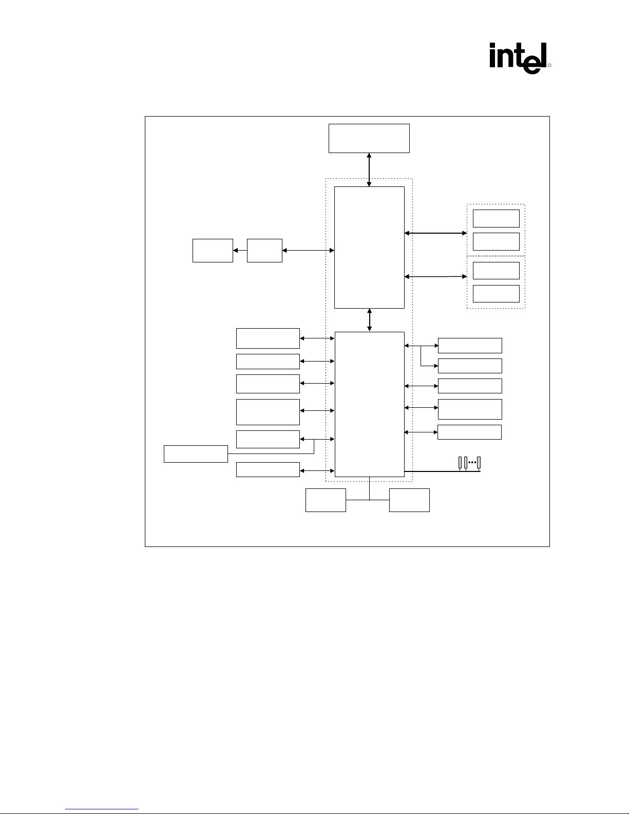
Figure 1-1. Intel
®
925X/925XE Express Chipset System Block Diagram Example
®
Intel
Pentium® 4
Processor
200/266 MHz FSB
Display
Intel® PCI Express
Gigabit Ethernet
Graphics
Card
USB 2.0
8 ports, 480 Mb/s
IDE
4 SATA Ports
150 MB/s
AC '97/Intel® High
Defini tion Audio
CODECs
PCI Express* x1
GPIO
PCI Express
x16 Graphics
(800/1066 MT/s)
Intel® 82925X MCH/
Intel® 82925XE MCH
DMI Interface
Intel® ICH6 Family
Intel® 925X/925XE Express Chipset
Channel A
Channel B
Power Management
Clock Gener a tion
LAN Connect/ASF
System
Management ( TCO)
SMBus 2.0/I2C
Seven PCI Masters
PCI Bus
System Memory
DDR2
DDR2
DDR2
DDR2
Note: 266 MHz ( 10 66 MT/s) FSB is for 82925XE MCH only
14 Intel
Flash
BIOS
LPC
Interface
SIO
Sys_Blk_P
®
82925X/82925XE MCH Datasheet
Page 15

Introduction
R
1.1 Terminology
Term Description
Core
DBI
DDR2
DMI
FSB
Full Reset
Host
INTx
Intel® ICH6
MCH
MSI
PCI Express*
Primary PCI
SCI
Core refers to the internal base logic in the MCH.
Dynamic Bus Inversion.
A second generation Double Data Rate SDRAM memory technology.
®
The Direct Media Interface is the connection between the MCH and the Intel
Front Side Bus. The FSB is synonymous with Host or processor bus
Full reset is when PWROK is de-asserted. Warm reset is when both RSTIN# and
PWROK are asserted.
This term is used synonymously with processor.
An interrupt request signal where X stands for interrupts A,B,C and D.
Sixth generation I/O Controller Hub component that contains additional functionality
compared to previous ICH6s. The Intel
primary PCI interface, LPC interface, USB2, ATA-100, and other I/O functions. It
communicates with the MCH over a proprietary interconnect called DMI.
The Memory Controller Hub (MCH) component contains the processor interface and
DRAM controller. It may also contain an x16 PCI Express port (typically the external
graphics interface). It communicates with the I/O controller hub (ICH6*) and other I/O
controller hubs over the DMI interconnect.
Message Signaled Interrupt. A transaction initiated outside the host, conveying interrupt
information to the receiving agent through the same path that normally carries read and
write commands.
Third Generation Input Output (PCI Express) Graphics Attach called PCI Express
Graphics. A high-speed serial interface whose configuration is software compatible with
the existing PCI specifications. The specific PCI Express implementation intended for
connecting the MCH to an external graphics controller is a x16 link and replaces AGP.
The physical PCI bus that is driven directly by the ICH6 component. Communication
between Primary PCI and the MCH occurs over DMI. Note that the Primary PCI bus is
not PCI Bus 0 from a configuration standpoint.
System Control Interrupt. SCI is used in ACPI protocol.
®
I/O Controller Hub component contains the
ICH6.
SERR
SMI
Rank
TOLM
VCO
®
Intel
82925X/82925XE MCH Datasheet 15
An indication that an unrecoverable error has occurred on an I/O bus.
System Management Interrupt. SMI is used to indicate any of several system conditions
(such as thermal sensor events, throttling activated, access to System Management
RAM, chassis open, or other system state related activity).
A unit of DRAM corresponding to eight x8 SDRAM devices in parallel or four x16
SDRAM devices in parallel, ignoring ECC. These devices are usually, but not always,
mounted on a single side of a DIMM.
Top Of Low Memory. The highest address below 4 GB for which a processor-initiated
memory read or write transaction will create a corresponding cycle to DRAM on the
memory interface.
Voltage Controlled Oscillator.
Page 16

Introduction
1.2 Reference Documents
Document Title Document Number/Location
Intel® 925X/925XE Express Chipset Thermal Design Guide http://intel.com/design/chipsets/
Intel® I/O Controller Hub 6 (ICH6) Family Datasheet http://intel.com/design/chipsets/
Advanced Configuration and Power Interface Specification, Version 2.0 http://www.acpi.info/
Advanced Configuration and Power Interface Specification, Version
1.0b
The PCI Local Bus Specification, Version 2.3 http://www.pcisig.com/specificat
PCI Express* Specification, Version 1.0a http://www.pcisig.com/specificat
R
designex/301466.htm
datashts/301473.htm
http://www.acpi.info/
ions
ions
1.3 MCH Overview
The MCH connects to the processor as shown in Figure 1-1. A major role of the MCH in a system
is to manage the flow of information between its interfaces: the processor interface (FSB), the
System Memory interface (DRAM controller), the external graphics interface via PCI Express,
and the I/O Controller Hub through the DMI interface. This includes arbitrating between the
interfaces when each initiates transactions. The processor interface supports the Pentium 4
processor subset of the Extended Mode of the Scalable Bus Protocol.
The MCH supports one or two channels of DDR2 SDRAM. The MCH also supports the new PCI
Express based external graphics attach. Thus, the 925X/925XE Express chipset is not compatible
with AGP (1X, 2X, 4X, or 8X).
To increase system performance, the MCH incorporates several queues and a write cache. The
MCH also contains advanced desktop power management logic.
1.3.1 Host Interface
The MCH is optimized for the Pentium 4 processors in the LGA775 socket. The 82925X MCH
supports a FSB frequency of 200 MHz (800 MT/s) using a scalable FSB. The 82925XE MCH
supports a FSB frequency of 266 MHz (1066 MT/s).
The MCH supports the Pentium 4 processor subset of the Extended Mode Scaleable Bus Protocol.
The primary enhancements over the Compatible Mode P6 bus protocol are: Source synchronous
double-pumped (2) Address and Source synchronous quad-pumped (4x) Data.
The MCH supports 32-bit host addressing, decoding up to 4 GB of the processor’s memory
address space. Host-initiated I/O cycles are decoded to PCI Express, DMI, or the MCH
configuration space. Host-initiated memory cycles are decoded to PCI Express, DMI, or system
memory. PCI Express device accesses to non-cacheable system memory are not snooped on the
host bus. Memory accesses initiated from PCI Express using PCI semantics and from DMI to
system memory will be snooped on the host bus.
16 Intel
®
82925X/82925XE MCH Datasheet
Page 17

Introduction
R
1.3.2 System Memory Interface
The MCH integrates a system memory DDR2 controller with two, 64-bit wide interfaces. Only
Double Data Rate (DDR2) memory is supported; consequently, the buffers support only
SSTL_1.8 V signal interfaces. The memory controller interface is fully configurable through a set
of control registers. Features of the MCH memory controller include:
• The MCH System Memory Controller directly supports one or two channels of memory
(each channel consisting of 64 data lines).
• Supports two memory addressing organization options:
⎯ The memory channels are asymmetric: "Stacked" channels are assigned addresses
serially. Channel B addresses are assigned after all Channel A addresses.
⎯ The memory channels are interleaved: Addresses are ping-ponged between the channels
after each cache line (64-B boundary).
• Available bandwidth up to:
⎯ 3.2 GB/s (DDR2 400) for single-channel mode
⎯ 6.4 GB/s in dual-channel interleaved mode assuming DDR2 400 MHz.
⎯ 8.5 GB/s in dual-channel interleaved mode assuming DDR2 533 MHz.
• Supports DDR2 memory DIMM frequencies of 400 MHz and 533 MHz. The speed used in
all channels is the speed of the slowest DIMM in the system.
• I/O Voltage of 1.8 V for DDR2.
• I/O Voltage of 1.9 V for DDR2 533 MHz CL3-3-3.
• Supports non-ECC and ECC (925X only) memory.
• Supports 256-Mb, 512-Mb and 1-Gb DDR2 technologies
• Supports only x8, x16, DDR2 devices with four banks and also supports eight bank,
1-Gbit DDR2 devices.
• Supports opportunistic refresh
• In dual channel mode the MCH supports 64 simultaneously open pages (four ranks of eight
bank devices* 2 channels)
• Supports Partial Writes to memory using Data Mask (DM) signals.
• Supports page sizes of 4 KB, 8 KB, and 16 KB.
• Supports a burst length of 8 for single-channel and dual-channel interleaved and asymmetric
operating modes.
• Supports unbuffered DIMMs.
• SPD (Serial Presence Detect) scheme for DIMM detection support
• Suspend-to-RAM support using CKE
• Supports configurations defined in the JEDEC DDR2 DIMM specification only
The MCH supports a memory thermal management scheme to selectively manage reads and/or
writes. Memory thermal management can be triggered either by on-die thermal sensor, or by
preset limits. Management limits are determined by weighted sum of various commands that are
scheduled on the memory interface.
®
Intel
82925X/82925XE MCH Datasheet 17
Page 18

Introduction
1.3.3 Direct Media Interface (DMI)
Direct Media Interface (DMI) is the chip-to-chip connection between the MCH and ICH6. This
high-speed interface integrates advanced priority-based servicing allowing for concurrent traffic
and true isochronous transfer capabilities. Base functionality is completely software transparent
permitting current and legacy software to operate normally.
To provide for true isochronous transfers and configurable Quality of Service (QoS) transactions,
the ICH6 supports two virtual channels on DMI: VC0 and VC1. These two channels provide a
fixed arbitration scheme where VC1 is always the highest priority. VC0 is the default conduit of
traffic for DMI and is always enabled. VC1 must be specifically enabled and configured at both
ends of the DMI link (i.e., the ICH6 and MCH). Features of the DMI include:
• A chip-to-chip connection interface to ICH6
• 2 GB/s point-to-point DMI to ICH6 (1 GB/s each direction)
• 100 MHz reference clock (shared with PCI Express Graphics Attach).
• 32-bit downstream addressing
• APIC and MSI interrupt messaging support. Will send Intel-defined “End Of Interrupt”
broadcast message when initiated by the processor.
• Message Signaled Interrupt (MSI) messages
• SMI, SCI and SERR error indication
• Legacy support for ISA regime protocol (PHOLD/PHOLDA) required for parallel port
DMA, floppy drive, and LPC bus masters
R
1.3.4 PCI Express* Graphics Interface
The MCH contains a 16-lane (x16) PCI Express* port intended for an external PCI Express
.
graphics card
Revision 1.0a. The x16 port operates at a frequency of 2.5 Gb/s on each lane while employing
8b/10b encoding, and supports a maximum theoretical bandwidth of 4 Gb/s each direction.
The PCI Express port is compatible with the PCI Express Base Specification
18 Intel
®
82925X/82925XE MCH Datasheet
Page 19

Introduction
R
Features of the PCI Express Interface include:
• One x16 PCI Express port intended for graphics attach, compatible with the PCI Express
Base Specification revision 1.0a.
• Theoretical PCI Express transfer rate of 2.5 Gb/s.
• Raw bit-rate on the data pins of 2.5 Gb/s, resulting in a real bandwidth per pair of 250 MB/s
given the 8b/10b encoding used to transmit data across this interface
• Maximum theoretical realized bandwidth on the interface of 4 GB/s in each direction
simultaneously, for an aggregate of 8 GB/s when (1)x16.
• PCI Express Graphics Extended Configuration Space. The first 256 bytes of configuration
space alias directly to the PCI Compatibility configuration space. The remaining portion of
the fixed 4-KB block of memory-mapped space above that (starting at 100h) is known as
extended configuration space.
• PCI Express Enhanced Addressing Mechanism. Accessing the device configuration space in
a flat memory mapped fashion.
• Automatic discovery, negotiation, and training of link out of reset
• Supports traditional PCI style traffic (asynchronous snooped, PCI ordering)
• Supports traditional AGP style traffic (asynchronous non-snooped, PCI Express-relaxed
ordering)
• Hierarchical PCI-compliant configuration mechanism for downstream devices (i.e., normal
PCI 2.3 Configuration space as a PCI-to-PCI bridge)
• Supports “static” lane numbering reversal. This method of lane reversal is controlled by a
Hardware Reset strap, and reverses both the receivers and transmitters for all lanes (e.g.,
TX15->TX0, RX15->RX0). This method is transparent to all external devices and is different
than lane reversal as defined in the PCI Express Specification. In particular, link initialization
is not affected by static lane reversal.
1.3.5 System Interrupts
The MCH interrupt support includes:
• Supports both 8259 and Pentium 4 processor FSB interrupt delivery mechanisms.
• Supports interrupts signaled as upstream Memory Writes from PCI Express and DMI
⎯ MSIs routed directly to FSB
⎯ From I/OxAPICs
®
Intel
82925X/82925XE MCH Datasheet 19
Page 20

Introduction
1.3.6 MCH Clocking
The differential FSB clock (HCLKP/HCLKN) is set to 200 MHz on the 82925X MCH and
266 MHz on the 82925XE MCH. This supports FSB transfer rates of 800 MT/s for the 82925X
MCH and FSB transfer rates of 1066 MT/s for the 82925XE MCH. The Host PLL generates 2X,
4X, and 8X versions of the host clock for internal optimizations. The MCH core clock is
synchronized to the host clock.
The internal and external memory clocks of 133 MHz, 200 MHz, and 266 MHz are generated
from one of two MCH PLLs that use the host clock as a reference. This includes 2X and 4X for
internal optimizations.
The PCI Express core clock of 250 MHz is generated from a separate PCI Express PLL. This
clock uses the fixed 100 MHz Serial Reference Clock (GCLKP/GCLKN) for reference.
All of the above mentioned clocks are capable of tolerating Spread Spectrum clocking as defined
in the Clock Generator specification. Host, Memory, and PCI Express* x16 Graphics PLLs, and
all associated internal clocks are disabled until PWROK is asserted.
R
1.3.7 Power Management
MCH Power Management support includes:
• PC99 suspend to DRAM support (“STR”, mapped to ACPI state S3)
• SMRAM space remapping to A0000h (128 KB)
• Supports extended SMRAM space above 256 MB, additional 1-MB TSEG from the Base of
graphics stolen memory (BSM) when enabled, and cacheable (cacheability controlled by
processor)
• ACPI Rev 1.0 compatible power management
• Supports processor states: C0, C1, C2, C3, and C4
• Supports System states: S0, S1, S3, S4, and S5
• Supports processor Thermal Management 2 (TM2)
• Microsoft Windows NT* Hardware Design Guide v1.0 compliant
§
20 Intel
®
82925X/82925XE MCH Datasheet
Page 21

Signal Description
R
2 Signal Description
This chapter provides a detailed description of MCH signals. The signals are arranged in
functional groups according to their associated interface. The states of all of the signals during
reset are provided in the Section 2.9.
The following notations are used to describe the signal type:
I Input pin
O Output pin
I/O Bi-directional input/output pin
GTL+ Open Drain GTL+ interface signal. Refer to the GTL+ I/O Specification for
complete details. The MCH integrates GTL+ termination resistors, and supports
of from 0.83 V to 1.65 V (including guardbanding).
VTT
PCIE PCI-Express interface signals. These signals are compatible with PCI Express
1.0 Signaling Environment AC Specifications and are AC coupled. The buffers
are not 3.3 V tolerant. Differential voltage specification
= (|D+ - D-|) * 2 = 1.2 V maximum Single-ended maximum = 1.5 V.
Single-ended minimum = 0 V.
DMI Direct Media Interface signals. These signals are compatible with PCI Express
1.0 Signaling Environment AC Specifications, but are DC coupled. The buffers
are not 3.3 V tolerant. Differential voltage specification
= (|D+ - D-|) * 2 = 1.2 V maximum. Single-ended maximum = 1.5 V.
Single-ended minimum = 0 V.
CMOS CMOS buffers. 1.5 V tolerant.
COD CMOS Open Drain buffers. 2.5 V tolerant.
HVCMOS High Voltage CMOS buffers. 2.5 V tolerant.
HVIN High Voltage CMOS input-only buffers. 3.3 V tolerant.
SSTL-1.8 Stub Series Termination Logic. These are 1.8 V output capable buffers; 1.8 V
tolerant. An I/O voltage of 1.9 V is needed for D DR2 533 MHz CL3-3-3.
A Analog reference or output. May be used as a threshold voltage or for buffer
compensation.
®
Intel
82925X/82925XE MCH Datasheet 21
Page 22
Signal Description
R
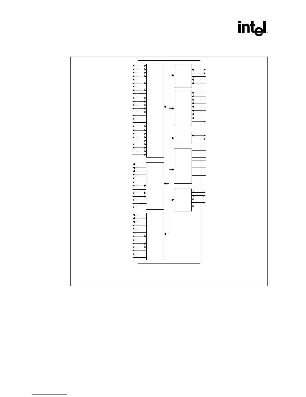
Figure 2-1. Intel
®
82925X/82925XE MCH Signal Interface Diagram
HA[31:3]#
HD[63:0]
HADS#
HBNR#
HBPRI#
HDBSY#
HDEFER#
HDRDY#
HEDRDY#
HHIT#
HHITM#
HLOCK#
HREQ[4:0]#
HPCREQ#
HTRDY#
HRS[2:0]#
HCPURST#
HBREQ0#
HDINV[3:0]#
HDSTBP[3:0]#, HDSTBN[3:0]#
SDQS_A[8:0], SDQS_A[8:0]#
SCLK_A[5:0], SCLK_A[5:0]#
SDQS_B[8:0], SDQS_B[8:0]#
SCLK_B[5:0], SCLK_B[5:0]#
HADSTB[1:0]#
BSEL[2:0]
HRCOMP
HSCOMP
HSWING
HVREF
SCS_A[3:0]#
SMA_A[13:0]
SBS_A[2:0]
SRAS_A#
SCAS_A#
SWE_A#
SDQ_A[63:0]
SDM_A[7:0]
SCB_A[7:0]
SCKE_A[3:0]
SODT_A[3:0]
SCS_B[3:0]#
SMA_B[13:0]
SBS_B_B[2:0]
SRAS_B#
SCAS_B#
SWE_B#
SDQ_B[63:0]
SDM_B[7:0]
SCB_B[7:0]
SCKE_B[3:0]
SODT_B[3:0]
Processor
System
Bus
Interface
System
Memory
DDR2
Channel
A
System
Memory
DDR2
Channel
B
PCI
Express
x16
Graphics
Port
Clocks,
Reset, and
Misc.
Direct
Media
Interface
Voltage
Reference,
and Powe r
System
Memory
DDR2 Ref./
Comp.
EXP_RXN[15:0], EXP_RXP[15:0]
EXP_TXN[15:0], EXP_TXP[15:0]
EXP_COMPO
EXP_COMPI
EXP_SLR
HCLKP, HCLKN
GCLKP, GCLKN
DREFCLKN, DREFCLKP
RSTIN#
PWROK
EXTTS#
BSEL[2:0]
MTYPE
ICH_SYNC#
DMI_RXP[3:0 ], DM I_ RXN[3:0]
DMI_TXP[3:0], DMI_TXN[3:0]
VCC
VTT
VCC_EXP
VCCSM
VCC2
VCCA_EXPPLL
VCCA_HPLL
VCCA_SMPLL
VSS
SRCOMP[1:0]
SOCOMP[1:0]
SM_SLEWIN[1:0]
SM_SLEWOUT[1:0]
SMVREF[1:0]
Note:
1. SCB_A[7:0] an d SCB_B[7:0] are on the Intel
2. SDQS_A8/SDQS_A8# and SDQS_B8/SDQS_B8# are on the Intel® 8 2925X only.
22 Intel
®
82925X only.
Signal_Info
®
82925X/82925XE MCH Datasheet
Page 23

Signal Description
R
2.1 Host Interface Signals
Note: Unless otherwise noted, the voltage level for all signals in this interface is tied to the termination
voltage of the Host Bus (V
Signal Name Type Description
).
TT
HADS# I/O
GTL+
HBNR# I/O
GTL+
HBPRI# O
GTL+
HBREQ0# I/O
GTL+
HCPURST# O
GTL+
HDBSY# I/O
GTL+
HDEFER# O
GTL+
HDINV[3:0]# I/O
GTL+
Address Strobe: The processor bus owner asserts HADS# to indicate the
first of two cycles of a request phase. The MCH can assert this signal for
snoop cycles and interrupt messages.
Block Next Request: This signal is used to block the current request bus
owner from issuing new requests. This signal is used to dynamically control
the processor bus pipeline depth.
Priority Agent Bus Request: The MCH is the only Priority Agent on the
processor bus. It asserts this signal to obtain the ownership of the address
bus. This signal has priority over symmetric bus requests and will cause the
current symmetric owner to stop issuing new transactions unless the
HLOCK# signal was asserted.
Bus Request 0: The MCH pulls the processor’s bus HBREQ0# signal low
during HCPURST#. The processor samples this signal on the active-toinactive transition of HCPURST#. The minimum setup time for this signal is
4 HCLKs. The minimum hold time is 2 clocks and the maximum hold time is
20 HCLKs. HBREQ0# should be tri-stated after the hold time requirement
has been satisfied.
CPU Reset: The HCPURST# pin is an output from the MCH. The MCH
asserts HCPURST# while RSTIN# is asserted and for approximately 1 ms
after RSTIN# is de-asserted. The HCPURST# allows the processors to
begin execution in a known state.
Note that the Intel
up and hold times around HCPURST#. This requires strict synchronization
between MCH HCPURST# de-assertion and the Intel® ICH6 driving the
straps.
Data Bus Busy: This signal is used by the data bus owner to hold the data
bus for transfers requiring more than one cycle.
Defer: Signals that the MCH will terminate the transaction currently being
snooped with either a deferred response or with a retry response.
Dynamic Bus Inversion: Driven along with the HD[63:0] signals. Indicates
if the associated signals are inverted or not. HDINV[3:0]# are asserted such
that the number of data bits driven electrically low (low voltage) within the
corresponding 16 bit group never exceeds 8.
HDINVx# Data Bits
HDINV3# HD[63:48]
HDINV2# HD[47:32]
HDINV1# HD[31:16]
HDINV0# HD[15:0]
®
ICH6 must provide processor frequency select strap set-
®
Intel
82925X/82925XE MCH Datasheet 23
Page 24

Signal Description
R
Signal Name Type Description
HDRDY# I/O
GTL+
HEDRDY# O
GTL+
HA[31:3]# I/O
GTL+
HADSTB[1:0]# I/O
GTL+
HD[63:0] I/O
GTL+
HDSTBP[3:0]#
HDSTBN[3:0]#
HHIT# I/O
HHITM# I/O
HLOCK# I/O
HPCREQ# I
I/O
GTL+
GTL+
GTL+
GTL+
GTL+
2x
Data Ready: This signal is asserted for each cycle that data is transferred.
Early Data Ready: This signal indicates that the data phase of a read
transaction will start on the bus exactly one common clock after assertion.
Host Address Bus: HA[31:3]# connect to the processor address bus.
During processor cycles, the HA[31:3]# are inputs. The MCH drives
HA[31:3]# during snoop cycles on behalf of DMI and PCI Express Graphics
initiators. HA[31:3]# are transferred at 2x rate.
Host Address Strobe: The source synchronous strobes used to transfer
HA[31:3]# and HREQ[4:0] at the 2x transfer rate.
Host Data: These signals are connected to the processor data bus. Data on
HD[63:0] is transferred at 4x rate. Note that the data signals may be
inverted on the processor bus, depending on the HDINV[3:0]# signals.
Differential Host Data Strobes: The differential source synchronous
strobes are used to transfer HD[63:0]# and HDINV[3:0]# at 4x transfer rate.
These signals are named this way because they are not level sensitive.
Data is captured on the falling edge of both strobes. Hence, they are
pseudo-differential, and not true differential.
Strobes Data Bits
HDSTBP3#, HDSTBN3# HD[63:48] HDINV3#
HDSTBP2#, HDSTBN2# HD[47:32] HDINV2#
HDSTBP1#, HDSTBN1# HD[31:16] HDINV1#
HDSTBP0#, HDSTBN0# HD[15:0] HDINV0#
Hit: This signal indicates that a caching agent holds an unmodified version
of the requested line. Also, driven in conjunction with HHITM# by the target
to extend the snoop window.
Hit Modified: This signal indicates that a caching agent holds a modified
version of the requested line and that this agent assumes responsibility for
providing the line. This signal is also driven in conjunction with HHIT# to
extend the snoop window.
Host Lock: All processor bus cycles sampled with the assertion of HLOCK#
and HADS#, until the negation of HLOCK# must be atomic (i.e., no DMI or
PCI Express Graphics accesses to DRAM are allowed when HLOCK# is
asserted by the processor).
Precharge Request: The processor provides a “hint” to the MCH that it is
OK to close the DRAM page of the memory read request with which the hint
is associated. The MCH uses this information to schedule the read request
to memory using the special “AutoPrecharge” attribute. This causes the
DRAM to immediately close (Precharge) the page after the read data has
been returned. This allows subsequent processor requests to more quickly
access information on other DRAM pages, since it will no longer be
necessary to close an open page prior to opening the proper page.
Asserted by the requesting agent during both halves of Request Phase. The
same information is provided in both halves of the request phase.
24 Intel
®
82925X/82925XE MCH Datasheet
Page 25

Signal Description
R
Signal Name Type Description
HREQ[4:0]# I/O
GTL+
2x
HTRDY# O
GTL+
HRS[2:0]# O
GTL+
BSEL[2:0] I
CMOS
HRCOMP I/O
CMOS
HSCOMP I/O
CMOS
HSWING I
HVREF I
Host Request Command: These signals define the attributes of the
request. HREQ[4:0]# are transferred at 2x rate. They are asserted by the
requesting agent during both halves of Request Phase. In the first half the
signals define the transaction type to a level of detail that is sufficient to
begin a snoop request. In the second half the signals carry additional
information to define the complete transaction type.
The transactions supported by the MCH Host Bridge are defined in the Host
Interface section of this document.
Host Target Ready: This signal indicates that the target of the processor
transaction is able to enter the data transfer phase.
Response Signals: These signals indicate the type of response as shown
below:
000 = Response type
001 = Idle state
010 = Retry response
011 = Deferred response
100 = Reserved (not driven by MCH)
101 = Hard Failure (not driven by MCH)
110 = No data response
111 = Implicit Writeback
111 = Normal data response
Bus Speed Select: At the de-assertion of RSTIN#, the value sampled on
these pins determines the expected frequency of the bus.
Host RCOMP: Used to calibrate the Host GTL+ I/O buffers.
This signal is powered by the Host Interface termination rail (VTT).
Slew Rate Compensation: Compensation for the Host Interface.
Host Voltage Swing: This signal provides the reference voltage used by
FSB RCOMP circuits. HSWING is used for the signals handled by
A
HRCOMP.
Host Reference Voltage Reference: Voltage input for the data, address,
and common clock signals of the Host GTL interface.
A
®
Intel
82925X/82925XE MCH Datasheet 25
Page 26

Signal Description
2.2 DDR2 DRAM Channel A Interface
Signal Name Type Description
R
SCLK_A[5:0] O
SSTL-1.8
SCLK_A[5:0]# O
SSTL-1.8
SCS_A[3:0]# O
SSTL-1.8
SMA_A[13:0] O
SSTL-1.8
SBS_A[2:0] O
SSTL-1.8
SRAS_A# O
SSTL-1.8
SCAS_A# O
SSTL-1.8
SWE_A# O
SSTL-1.8
SDQ_A[63:0] I/O
SSTL-1.8
2x
SDM_A[7:0] O
SSTL-1.8
2X
SCB_A[7:0]
®
(Intel
82925X
Only)
SDQS_A[8:0]
(82925X MCH)
SDQS_A[7:0]
(82925XE
MCH)
SDQS_A[8:0]#
(82925X MCH)
SDQS_A[7:0]#
(82925XE
MCH)
SCKE_A[3:0] O
SODT_A[3:0] O
I/O
SSTL-1.8
2X
I/O
SSTL-1.8
2x
I/O
SSTL-1.8
2x
SSTL-1.8
SSTL-1.8
SDRAM Differential Clock: (3 per DIMM). SCLK_Ax and its
complement SCLK_Ax# signal make a differential clock pair output. The
crossing of the positive edge of SCLK_Ax and the negative edge of its
complement SCLK_Ax# are used to sample the command and control
signals on the SDRAM.
SDRAM Complementary Differential Clock: (3 per DIMM) These are
the complementary differential DDR2 Clock signals.
Chip Select: (1 per Rank) These signals select particular SDRAM
components during the active state. There is one chip select for each
SDRAM rank.
Memory Address: These signals are used to provide the multiplexed
row and column address to the SDRAM
Bank Select: These signals define which banks are selected within each
SDRAM rank
DDR2: 1-Gb technology is 8 banks.
Row Address Strobe: This signal is used with SCAS_A# and SWE_A#
(along with SCS_A#) to define the SDRAM commands.
Column Address Strobe: This signal is used with SRAS_A# and
SWE_A# (along with SCS_A#) to define the SDRAM commands.
Write Enable: This signal is used with SCAS_A# and SRAS_A# (along
with SCS_A#) to define the SDRAM commands.
Data Lines: SDQ_A signals interface to the SDRAM data bus.
Data Mask: When activated during writes, the corresponding data
groups in the SDRAM are masked. There is one SDM_Ax signal for
every data byte lane.
ECC Check Byte: These signals require a 6-layer board to be routed.
Data Strobes: For DDR2, SDQS_Ax and its complement SDQS_Ax#
signal make up a differential strobe pair. The data is captured at the
crossing point of SDQS_Ax and its complement SDQS_Ax# during read
and write transactions.
Data Strobe Complements: These signals are the complementary
DDR2 strobe signals.
Clock Enable: (1 per Rank) SACKE is used to initialize the SDRAMs
during power-up, to power-down SDRAM ranks, and to place all SDRAM
ranks into and out of self-refresh during Suspend-to-RAM.
On Die Termination: Active On-die Termination Control signals for
DDR2 devices.
26 Intel
®
82925X/82925XE MCH Datasheet
Page 27

Signal Description
R
2.3 DDR2 DRAM Channel B Interface
Signal Name Type Description
SCLK_B[5:0] O
SSTL-1.8
SCLK_B[5:0]# O
SSTL-1.8
SCS_B[3:0]# O
SSTL-1.8
SMA_B[13:0] O
SSTL-1.8
SBS_B[2:0] O
SSTL-1.8
SRAS_B# O
SSTL-1.8
SCAS_B# O
SSTL-1.8
SWE_B# O
SSTL-1.8
SDQ_B[63:0] I/O
SSTL-1.8
2x
SDM_B[7:0] O
SSTL-1.8
2x
SCB_B[7:0]
®
(Intel
82925X
Only)
SDQS_B[8:0]
(82925X MCH)
SDQS_B[7:0]
(82925XE MCH)
SDQS_B[8:0]#
(82925X MCH)
SDQS_B[7:0]#
(82925XE MCH)
SCKE_B[3:0] O
SODT_B[3:0] O
I/O
SSTL-1.8
2X
I/O
SSTL-1.8
2x
I/O
SSTL-1.8
2x
SSTL-1.8
SSTL-1.8
SDRAM Differential Clock: (3 per DIMM) SCLK_Bx and its complement
SCLK_Bx# signal make a differential clock pair output. The crossing of
the positive edge of SCLK_Bx and the negative edge of its complement
SCLK_Bx# are used to sample the command and control signals on the
SDRAM.
SDRAM Complementary Differential Clock: (3 per DIMM) These are
the complementary differential DDR2 clock signals.
Chip Select: (1 per Rank) These signals select particular SDRAM
components during the active state. There is one chip select for each
SDRAM rank
Memory Address: These signals are used to provide the multiplexed
row and column address to the SDRAM
Bank Select: These signals define which banks are selected within
each SDRAM rank
DDR2: 1-Gb technology is 8 banks.
Row Address Strobe: This signal is used with SCAS_B# and SWE_B#
(along with SCS_B#) to define the SDRAM commands
Column Address Strobe: This signal is used with SRAS_B# and
SWE_B# (along with SCS_B#) to define the SDRAM commands.
Write Enable: This signal is used with SCAS_B# and SRAS_B# (along
with SCS_B#) to define the SDRAM commands.
Data Lines: SDQ_Bx signals interface to the SDRAM data bus
Data Mask: When activated during writes, the corresponding data
groups in the SDRAM are masked. There is one SDM_Bx signal for
every data byte lane.
ECC Check Byte: These signals require a 6-layer board to be routed.
Data Strobes: For DDR2, SDQS_Bx and its complement SDQS_Bx#
make up a differential strobe pair. The data is captured at the crossing
point of SDQS_Bx and its complement SDQS_Bx# during read and write
transactions.
Data Strobe Complements: These signals are the complementary
DDR2 strobe signals.
Clock Enable: (1 per Rank) SCKE_B is used to initialize the SDRAMs
during power-up, to power-down SDRAM ranks, and to place all SDRAM
ranks into and out of self-refresh during Suspend-to-RAM.
On Die Termination: Active On-die Termination Control signals for
DDR2 devices.
®
Intel
82925X/82925XE MCH Datasheet 27
Page 28

Signal Description
2.4 DDR2 DRAM Reference and Compensation
Signal Name Type Description
SRCOMP[1:0] I/O System Memory RCOMP
SOCOMP[1:0] I/O
SM_SLEWIN[1:0] I A Buffer Slew Rate Input: Slew Rate Characterization buffer input for X
SM_SLEWOUT[1:0] O A Buffer Slew Rate Output: Slew Rate Characterization buffer output for
DDR2 On-Die DRAM Over Current Detection (OCD) driver
A
compensation
and Y orientation.
X and Y orientation
R
SMVREF[1:0] I
SDRAM Reference Voltage: Reference voltage inputs for each DQ,
DM, DQS, and DQS# input signals.
A
2.5 PCI Express* x16 Graphics Port Signals
Unless otherwise specified, PCI Express Graphics signals are AC coupled, so the only voltage
specified is a maximum 1.2 V differential swing.
Signal Name Type Description
EXP_RXN[15:0]
EXP_RXP[15:0]
EXP_TXN[15:0]
EXP_TXP[15:0]
EXP_COMPO I A PCI Express Graphics Output Current Compensation
EXP_COMPI I A PCI Express Graphics Input Current Compensation
EXP_SLR I
I/O
PCIE
O
PCIE
CMOS
PCI Express Graphics Receive Differential Pair
PCI Express Graphics Transmit Differential Pair
Note: EXP_COMP0 is used for DMI current compensation.
Note: EXP_COMPI is used for DMI current compensation.
PCI Express* Static Lane Reversal: The MCH’s PCI Express lane
numbers are reversed. For example, the MCH PCI Express interface
signals can be configured as follows:
Normal Lane
Ball Operation Reversed
C10 EXP_TXP0 EXP_TXP15
A9 EXP_TXP1 EXP_TXP14
… … …
N3 EXP_TXP14… EXP_TXP1…
P1 EXP_TXP15 EXP_TXP0
0 = MCH’s PCI Express lane numbers are reversed
1 = Normal operation
28 Intel
®
82925X/82925XE MCH Datasheet
Page 29

Signal Description
R
2.6 Clocks, Reset, and Miscellaneous
Signal Name Type Description
HCLKP
HCLKN
GCLKP
GCLKN
DREFCLKN
DREFCLKP
RSTIN# I
PWROK I
EXTTS# I
MTYPE I
ICH_SYNC# O
I
CMOS
I
CMOS
I
CMOS
HVIN
HVIN
HVCMOS
CMOS
HVCMOS
Differential Host Clock In: These pins receive a differential host clock
from the external clock synthesizer. This clock is used by all of the MCH
logic that is in the Host clock domain.
Differential PCI Express Graphics Clock In: These pins receive a
differential 100 MHz serial reference clock from the external clock
synthesizer. This clock is used to generate the clocks necessary for the
support of PCI Express.
Display PLL Differential Clock In
Reset In: When asserted, this signal will asynchronously reset the MCH
logic. This signal is connected to the PLTRST# output of the Intel
All PCI Express Graphics Attach output signals will also tri-state
compatible with PCI Express* Specification Rev 1.0a.
This input should have a Schmitt trigger to avoid spurious resets.
This signal is required to be 3.3 V tolerant.
Power OK: When asserted, PWROK is an indication to the MCH that
core power has been stable for at least 10 us.
External Thermal Sensor Input: This signal may connect to a precision
thermal sensor located on or near the DIMMs. If the system temperature
reaches a dangerously high value, then this signal can be used to trigger
the start of system thermal management. This signal is activated when
an increase in temperature causes a voltage to cross some threshold in
the sensor.
Memory Type Select Strap. This signal is a strapping option that
indicates the type of system memory. This signal should be tied to
ground indicating DDR2 memory.
ICH Sync: This signal is connected to the MCH_SYNCH# signal on the
ICH6.
®
ICH6.
2.7 Direct Media Interface (DMI)
Signal Name Type Description
DMI_RXP[3:0]
DMI_RXN[3:0]
DMI_TXP[3:0]
DMI_TXN[3:0]
®
Intel
82925X/82925XE MCH Datasheet 29
I/O
DMI
O
DMI
Direct Media Interface: These signals are the receive differential
pair (Rx).
Direct Media Interface: These signals are the transmit differential
pair (Tx).
Page 30
Signal Description
2.8 Power and Ground
Name Voltage Description
VCC 1.5 V Core Power.
VTT 1.2 V Processor System Bus Power.
VCC_EXP 1.5 V PCI Express* and DMI Power.
VCCSM 1.8 V System Memory Power.
DDR2: VCCSM = 1.8 V (VCCSM = 1.9 V for DDR2 533 CAS 3-3-3)
VCC2 2.5 V 2.5 V CMOS Power.
VCCA_EXPPLL 1.5 V PCI Express PLL Analog Power.
VCCA_HPLL 1.5 V Host PLL Analog Power.
VCCA_SMPLL 1.5 V System Memory PLL Analog Power.
VSS 0 V Ground.
R
2.9 Reset States and Pull-up/Pull-downs
This section describes the expected states of the MCH I/O buffers during and immediately after
the assertion of RSTIN#. This table only refers to the contributions on the interface from the
MCH and does not reflect any external influence (such as external pull-up/pull-down resistors or
external drivers).
Legend:
CMCT: Common Mode Center Tapped. Differential signals are weakly driven to the common
mode central voltage.
DRIVE: Strong drive (to normal value supplied by core logic if not otherwise stated)
TERM: Normal termination devices are turned on
LV: Low voltage
HV: High voltage
IN: Input buffer enabled
ISO: Isolate input buffer so that it does not oscillate if input left floating
TRI: Tri-state
PU: Weak internal pull-up
PD: Weak internal pull-down
STRAP: Strap input sampled during assertion or on the de-asserting edge of RSTIN#
30 Intel
®
82925X/82925XE MCH Datasheet
Page 31

Signal Description
R
Table 2-1. Host Interface Reset and S3 States
Interface Signal Name I/O
Host I/F HCPURST# O DRIVE LV TERM HV after
HADSTB[1:0]# I/O TERM HV TERM HV TRI (No VTT)
HA[31:3]# I/O TERM HV TERM HV TRI (No VTT)
HD[63:0] I/O TERM HV TERM HV TRI (No VTT)
HDSTBP[3:0]# I/O TERM HV TERM HV TRI (No VTT)
HDSTBN[3:0]# I/O TERM HV TERM HV TRI (No VTT)
HDINV[3:0]# I/O TERM HV TERM HV TRI (No VTT)
HADS# I/O TERM HV TERM HV TRI (No VTT)
HBNR# I/O TERM HV TERM HV TRI (No VTT)
HBPRI# O TERM HV TERM HV TRI (No VTT)
HDBSY# I/O TERM HV TERM HV TRI (No VTT)
HDEFER# O TERM HV TERM HV TRI (No VTT)
HDRDY# I/O TERM HV TERM HV TRI (No VTT)
HEDRDY# O TERM HV TERM HV TRI (No VTT)
Host I/F HHIT# I/O TERM HV TERM HV TRI (No VTT)
HHITM# I/O TERM HV TERM HV TRI (No VTT)
HLOCK# I/O TERM HV TERM HV TRI (No VTT)
HREQ[4:0]# I/O TERM HV TERM HV TRI (No VTT)
HTRDY# O TERM HV TERM HV TRI (No VTT)
HRS[2:0]# O TERM HV TERM HV TRI (No VTT)
HBREQ0# I/O TERM HV TERM HV TRI (No VTT)
HPCREQ# I TERM HV TERM HV TRI (No VTT)
HVREF I IN IN TRI
HRCOMP I/O TRI TRI after RCOMP TRI 20 Ω resistor
HSWING I IN IN
HSCOMP I/O TRI TRI TRI
State During
RSTIN#
Assertion
State After
RSTIN# De-
assertion
approximately 1ms
S3
TRI (No VTT)
Pull-up/
Pull-down
for board with
target
impedance of
60 Ω
®
Intel
82925X/82925XE MCH Datasheet 31
Page 32

Signal Description
Table 2-2. System Memory Reset and S3 States
R
Interface Signal Name I/O
System
Memory
System
Memory
Channel A
SCLK_A[5:0] O TRI TRI TRI
SCLK_A[5:0]# O TRI TRI TRI
SCS_A[3:0]# O TRI TRI TRI
SMA_A[13:0] O TRI TRI TRI
SBS_A[2:0] O TRI TRI TRI
SRAS_A# O TRI TRI TRI
SCAS_A# O TRI TRI TRI
SWE_A# O TRI TRI TRI
SDQ_A[63:0] I/O TRI TRI TRI
SDM_A[7:0] O TRI TRI TRI
SCB_A[7:0]1 I/O TRI TRI TRI
SDQS_A[8:0] 2 I/O TRI TRI TRI
SDQS_A[8:0]# 2 I/O TRI TRI TRI
SCKE_A[3:0] O LV LV LV
SODT_A[3:0] O LV LV LV
Channel B
SCLK_B[5:0] O TRI TRI TRI
SCLK_B[5:0]# O TRI TRI TRI
SCS_B[3:0]# O TRI TRI TRI
SMA_B[13] O TRI TRI TRI
SMA_B[12:11] O LV LV LV
SMA_B[10:8] O TRI TRI TRI
SMA_B[7] O LV LV LV
SMA_B[6:0] O TRI TRI TRI
SBS_B[2] O LV LV LV
SBS_B[1:0] O TRI TRI TRI
SRAS_B# O TRI TRI TRI
SCAS_B# O TRI TRI TRI
SWE_B# O TRI TRI TRI
SDQ_B[63:0] I/O TRI TRI TRI
SDM_B[7:0] O TRI TRI TRI
SCB_B[7:0] 1 I/O TRI TRI TRI
2
SDQS_B[8:0]
I/O TRI TRI TRI
State During
RSTIN#
Assertion
State After
RSTIN# De-
assertion
S3
Pull-up/
Pull-down
32 Intel
®
82925X/82925XE MCH Datasheet
Page 33

Signal Description
R
Interface Signal Name I/O
SDQS_B[8:0]# 2 I/O TRI TRI TRI
SCKE_B[3:0] O LV LV LV
SODT_B[3:0] O LV LV LV
SRCOMP0 I/O TRI TRI (after RCOMP) TRI
SRCOMP1 I/O TRI TRI (after RCOMP) TRI
SM_SLEWIN[1:0] I IN IN IN
SM_SLEWOU[1:0] O TRI TRI (after RCOMP) TRI
SMVREF[1:0] I IN IN IN
SOCOMP[1:0] I/O TRI TRI TRI DDR2: 40 Ω
NOTES:
1. These signals are on the 82925X MCH only.
2. SDQS_A8/SDQS_A8# and SDQS_B8/SDQS_B8# are on the 82925X MCH only.
State During
RSTIN#
Assertion
State After
RSTIN# De-
assertion
Table 2-3. PCI Express* Graphics x16 Port Reset and S3 States
Interface Signal Name I/O
State During
RSTIN#
Assertion
State After RSTIN#
De-assertion
S3
S3
Pull-up/
Pull-down
resistor to
ground
Pull-up/
Pull-down
PCI
Express*Graphics
EXP_RXN[15:0] I/O CMCT CMCT CMCT
EXP_RXP[15:0] I/O CMCT CMCT CMCT
EXP_TXN[15:0] O CMCT 1.0 V CMCT 1.0 V CMCT 1.0 V
EXP_TXP[15:0] O CMCT 1.0 V CMCT 1.0 V CMCT 1.0 V
EXP_COMPO I TRI TRI (after RCOMP) TRI
EXP_COMPI I TRI TRI (after RCOMP) TRI
Table 2-4. DMI Reset and S3 States
Interface Signal Name I/O
DMI
DMI_RXN[3:0] I/O CMCT CMCT CMCT
DMI_RXP[3:0] I/O CMCT CMCT CMCT
DMI_TXN[3:0] O CMCT 1.0 V CMCT 1.0 V CMCT 1.0 V
DMI_TXP[3:0] O CMCT 1.0 V CMCT 1.0 V CMCT 1.0 V
State During
RSTIN#
Assertion
State After RSTIN#
De-assertion
S3
Pull-up/ Pull-
down
®
Intel
82925X/82925XE MCH Datasheet 33
Page 34

Signal Description
Table 2-5. Clocking Reset and S3 States
R
Interface Signal Name I/O
Clocks
HCLKN I IN IN IN
HCLKP I IN IN IN
GCLKN I IN IN IN
GCLKP I IN IN IN
DREFCLKN I IN IN IN
DREFCLKP I IN IN IN
State During
RSTIN#
Assertion
Table 2-6. Miscellaneous Reset and S3 States
Interface Signal Name I/O
Misc.
RSTIN# I IN IN IN
PWROK I HV HV HV
EXTTS# I PU PU PU
BSEL[2:0] I TRI TRI TRI
MTYPE I TERM HV TERM HV TERM HV
EXP_SLR I TERM HV TERM HV TERM HV
ICH_SYNC# O PU PU PU
State During
RSTIN#
Assertion
State After
RSTIN# De-
assertion
State After RSTIN#
De-assertion
S3
S3
Pull-up/
Pull-down
Pull-up/
Pull-down
§
34 Intel
®
82925X/82925XE MCH Datasheet
Page 35

Register Description
R
3 Register Description
The MCH contains two sets of software accessible registers, accessed via the processor I/O
address space: Control registers and internal configuration registers.
• Control registers are I/O mapped into the processor I/O space that control access to PCI and
PCI Express configuration space (see Section 3.4).
• Internal configuration registers residing within the MCH are partitioned into two logical
device register sets (“logical” since they reside within a single physical device). The first
register set is dedicated to Host Bridge functionality (i.e. DRAM configuration , other chip-set
operating parameters and optional features). The second register block is dedicated to HostPCI Express Bridge functions (controls PCI Express interface configurations and operating
parameters).
The MCH internal registers (I/O Mapped, Configuration and PCI Express Extended
Configuration registers) are accessible by the processor. The registers that reside within the lower
256 bytes of each device can be accessed as Byte, Word (16-bit), or DWord (32-bit) quantities,
with the exception of CONFIG_ADDRESS that can only be accessed as a DWord. All multi-byte
numeric fields use "little-endian" ordering (i.e., lower addresses contain th e least significant parts
of the field). Registers that reside in bytes 256 through 4095 of each device may only be accessed
using memory mapped transactions in DWord (32-bit) quantities.
3.1 Register Terminology
The following table shows the register-related terminology that is used.
Item Description
RO Read Only bit(s). Writes to these bits have no effect.
RS/WC Read Set / Write Clear bit(s). These bits are set to ‘1’ when read and then will continue
to remain set until written. A write of ‘1’ clears (sets to ‘0’) the corresponding bit(s) and a
write of ‘0’ has no effect.
R/W Read / Write bit(s). These bits can be read and written.
R/WC Read / Write Clear bit(s). These bits can be read. Internal events may set this bit. A
write of ‘1’ clears (sets to ‘0’) the corresponding bit(s) and a write of ‘0’ has no effect.
R/WC/S Read / Write Clear / Sticky bit(s). These bits can be read. Internal events may set this
bit. A write of ‘1’ clears (sets to ‘0’) the corresponding bit(s) and a write of ‘0’ has no
effect. Bits are not cleared by "warm" reset, but will be reset with a cold/complete reset
(for PCI Express* related bits a cold reset is “Power Good Reset” as defined in the PCI
Express* Specification).
R/W/L Read / Write / Lockable bit(s). These bits can be read and written. Additionally there is a
bit (which may or may not be a bit marked R/W/L) that, when set, prohibits this bit field
from being writeable (bit field becomes Read Only).
R/W/S Read / Write / Sticky bit(s). These bits can be read and written. Bits are not cleared by
"warm" reset, but will be reset with a cold/complete reset (for PCI Express related bits a
cold reset is “Power Good Reset” as defined in the PCI Express* Specification).
®
Intel
82925X/82925XE MCH Datasheet 35
Page 36

Register Description
R/WSC Read / Write Self Clear bit(s). These bits can be read and written. When the bit is ‘1’,
R/WSC/L Read / Write Self Clear / Lockable bit(s). These bits can be read and written. When the
R/WC Read Write Clear bit(s). These bits can be read and written. However, a write of ‘1’
R/WO Write Once bit(s). Once written, bits with this attribute become Read Only. These bits
W Write Only. Whose bits may be written, but will always-return zeros when read. They are
Reserved Bits Some of the MCH registers described in this section contain reserved bits. These bits
Reserved
Registers
Default Value Upon a Full Reset, the MCH sets its entire set of internal configuration registers to
R
Item Description
hardware may clear the bit to ‘0’ based upon internal events, possibly sooner than any
subsequent read could retrieve a ‘1’.
bit is ‘1’, hardware may clear the bit to ‘0’ based upon internal events, possibly sooner
than any subsequent read could retrieve a ‘1’. Additionally there is a bit (which may or
may not be a bit marked R/W/L) that, when set, prohibits this bit field from being
writeable (bit field becomes Read Only).
clears (sets to ‘0’) the corresponding bit(s) and a write of ‘0’ has no effect.
can only be cleared by a Reset.
used for write side effects. Any data written to these registers cannot be retrieved.
are labeled "Reserved”. Software must deal correctly with fields that are reserved. On
reads, software must use appropriate masks to extract the defined bits and not rely on
reserved bits being any particular value. On writes, software must ensure that the
values of reserved bit positions are preserved. That is, the values of reserved bit
positions must first be read, merged with the new values for other bit positions and then
written back. Note the software does not need to perform read, merge, and write
operation for the configuration address register.
In addition to reserved bits within a register, the MCH contains address locations in the
configuration space of the Host Bridge entity that are marked either "Reserved" or “Intel
Reserved”. The MCH responds to accesses to “Reserved” address locations by
completing the host cycle. When a “Reserved” register location is read, a zero value is
returned. (“Reserved” registers can be 8-, 16-, or 32-bits in size). Writes to “Reserved”
registers have no effect on the MCH. Registers that are marked as “Intel Reserved”
must not be modified by system software. Writes to “Intel Reserved” registers may
cause system failure. Reads from “Intel Reserved” registers may return a non-zero
value.
predetermined default states. Some register values at reset are determined by external
strapping options. The default state represents the minimum functionality feature set
required to successfully bringing up the system. Hence, it does not represent the
optimal system configuration. It is the responsibility of the system initialization software
(usually BIOS) to properly determine the DRAM configurations, operating parameters
and optional system features that are applicable, and to program the MCH registers
accordingly.
36 Intel
®
82925X/82925XE MCH Datasheet
Page 37

Register Description
R
3.2 Platform Configuration
In platforms that support DMI (e.g. this MCH) the configuration structure is significantly
different from previous Hub architectures. The DMI physically connects the MCH and the Intel
ICH6; so, from a configuration standpoint, the DMI is logically PCI bus 0. As a result, all devices
internal to the MCH and the Intel ICH6 appear to be on PCI bus 0.
The ICH6 internal LAN controller does not appear on bus 0; it appears on the external PCI bus
(whose number is configurable).
The system’s primary PCI expansion bus is physically attached to the Intel ICH6 and, from a
configuration perspective, appears to be a hierarchical PCI bus behind a PCI-to-PCI bridge and
therefore has a programmable PCI Bus number. The PCI Express Graphics Attach appears to
system software to be a real PCI bus behind a PCI-to-PCI bridge that is a device resident on PCI
bus 0.
Note: A physical PCI bus 0 does not exist and that DMI and the internal devices in the MCH and Intel
ICH6 logically constitute PCI Bus 0 to configuration software. This is shown in Figure 3-1.
Figure 3-1. Conceptual Intel
Diagram
®
925X/925XE Express Chipset Platform PCI Configuration
Processor
Intel® 82925X/82925XE MCH
DRAM Controller Interface
Bus 0, Device 0
Intel® ICH6
PCI Express* Bus 0, Device 1
PCI Configurati on Window in
I/O Space
DMI
PCI Configurati on Window in
I/O Space
®
Intel
82925X/82925XE MCH Datasheet 37
LPC Device Bus 0, Device 31
Functi on 0
DMI PCI Bridge (P2) Bus 0,
Device 30 Function0
PCI_Config_Dia
Page 38

Register Description
The MCH contains the following PCI devices within a single physical component. The
configuration registers for the devices are mapped as devices residing on PCI bus 0.
• Device 0 – Host Bridge/DRAM Controller: Logically this appears as a PCI device residing
on PCI bus 0. Device 0 contains the standard PCI header registers, PCI Express base address
register, DRAM control (including thermal/throttling control), and configu r ation for the DMI
and other MCH specific registers.
• Device 1– Host-PCI Express Bridge. Logically this appears as a “virtual” PCI-to-PCI
bridge residing on PCI bus 0 and is compliant with PCI Express* Specification Revision
1.0a. Device 1 contains the standard PCI-to-PCI bridge registers and the standard PCI
Express/PCI configuration registers (including the PCI Express memory address mapping). It
also contains Isochronous and Virtual Channel controls in the PCI Express extended
configuration space.
Table 3-1. Device Number Assignment for Internal MCH Devices
MCH Function Device#
Host Bridge / DRAM Controller Device 0
Host-to-PCI Express* Bridge (virtual P2P) Device 1
R
3.3 General Routing Configuration Accesses
The MCH supports two PCI related interfaces: DMI and PCI Express. PCI and PCI Express
configuration cycles are selectively routed to one of these interfaces. The MCH is responsible for
routing configuration cycles to the proper interface. Configuration cycles to the Intel ICH6
internal devices and Primary PCI (including downstream devices) are routed to the Intel ICH6 via
DMI. Configuration cycles to both the PCI Express Graphics PCI compatibility configuration
space and the PCI Express Graphics extended configuration space are routed to the PCI Express
Graphics port.
A detailed description of the mechanism for translating processor I/O bus cycles to configuration
cycles is described below.
3.3.1 Standard PCI Bus Configuration Mechanism
The PCI Bus defines a slot based "configuration space" that allows each device to contain up to 8
functions with each function containing up to 256 8-bit configuration registers. The PCI
specification defines two bus cycles to access the PCI configuration space: Configuration Read
and Configuration Write. Memory and I/O spaces are supported directly by the processor.
Configuration space is supported by a mapping mechanism implemented within the MCH.
The configuration access mechanism makes use of the CONFIG_ADDRESS Register (at I/O
address 0CF8h though 0CFBh) and CONFIG_DATA Register (at I/O address 0CFCh though
0CFFh). To reference a configuration register a DW I/O write cycle is used to place a value into
CONFIG_ADDRESS that specifies the PCI bus, the device on that bus, the function within the
device, and a specific configuration register of the device function being accessed.
CONFIG_ADDRESS [31] must be 1 to enable a configuration cycle. CONFIG_DATA then
becomes a window into the four bytes of configuration space specified by the contents of
38 Intel
®
82925X/82925XE MCH Datasheet
Page 39

Register Description
R
CONFIG_ADDRESS. Any read or write to CONFIG_DATA will result in the MCH translating
the CONFIG_ADDRESS into the appropriate configuration cycle.
The MCH is responsible for translating and routing the processor’s I/O accesses to the
CONFIG_ADDRESS and CONFIG_DATA registers to internal MCH configuration registers,
DMI, or PCI Express.
3.3.2 Logical PCI Bus 0 Configuration Mechanism
The MCH decodes the Bus Number (bits 23:16) and the Device Number fields of the
CONFIG_ADDRESS register. If the Bus Number field of CONFIG_ADDRESS is 0 the
configuration cycle is targeting a PCI Bus 0 device. The Host-DMI Bridge entity within the MCH
is hardwired as Device 0 on PCI Bus 0. The Host-PCI Express Bridge en tity within the MCH is
hardwired as Device 1 on PCI Bus 0. The Intel ICH6 decodes the Type 0 access and generates a
configuration access to the selected internal device.
3.3.3 Primary PCI and Downstream Configuration Mechanism
If the Bus Number in the CONFIG_ADDRESS is non-zero, and falls outside the range claimed
by the Host-PCI Express bridge (not between upper bound in device’s Subordinate Bus Number
register and lower bound in device’s Secondary Bus Number register), the MCH would generate a
Type 1 DMI configuration cycle. This DMI configuration cycle will be sent over the DMI.
If the cycle is forwarded to the Intel ICH6 via the DMI, the Intel ICH6 compares the non-zero
Bus Number with the Secondary Bus Number and Subordinate Bus Number registers of its P2P
bridges to determine if the configuration cycle is meant for ICH6 PCI Express ports one of the
Intel ICH6’s devices, the DMI, or a downstream PCI bus.
Figure 3-2. DMI Type 0 Configuration Address Translation
Configurati on Address
31 30 24 23 16 15
1
31 30 24 23 16 15
1
Reserved
OCFBh
Reserved
Bus Number
DMI Type 0 Configuration Address Extension
OCFAh OCF9h
Bus Number
Device
Number
Device
Number
11
10 87 21
Function
11
10 87 21 0
Function
Double
Word
OCF8h
Double
Word
XX
00
DMI_Typ0_Config
0
®
Intel
82925X/82925XE MCH Datasheet 39
Page 40

Register Description
Figure 3-3. DMI Type 1 Configuration Address Translation
Configurat ion Address
R
Device
Number
Device
Number
11
10 87 21
Function
11
10 87 21
Function
Double
Word
Double
Word
31 30 24 23 16 15
1
31 30 24 23 16 15
1
Reserved
OCFBh
Reserved
Bus Number
DMI Type 1 Configuration Address Ext ension
OCFAh OCF9h OCF8h
Bus Number
3.3.4 PCI Express* Enhanced Configuration Mechanism
PCI Express extends the configuration space to 4096 bytes per device/function as compared to
256 bytes allowed by PCI Specification, Revision 2.3. PCI Express configuration space is divided
into a PCI 2.3 compatible region that consists of the first 256B of a logical device’s configuration
space and a PCI Express extended region that consists of the remaining configuration space.
The PCI compatible region can be accessed using either the mechanism defined in the previous
section or using the enhanced PCI Express configuration access mechanism described in this
section. The extended configuration registers may only be accessed using the enhanced PCI
Express configuration access mechanism. To maintain compatibility with PCI configuration
addressing mechanisms, system software must access the extended configuration space using 32bit operations (32-bit aligned) only. These 32-bit operations include byte enables allowing only
appropriate bytes within the DWord to be accessed. Locked transactions to the PCI Express
memory mapped configuration address space are not supported. All changes made using either
access mechanism are equivalent. The enhanced PCI Express configuration access mechanism
uses a flat memory-mapped address space to access device configuration registers. This address
space is reported by the system firmware to the operating system. The PCIEXBAR register
defines the base address for the 256-MB block of addresses below top of addressable memory
(currently 4 GB) for the configuration space associated with all devices and functions that are
potentially a part of the PCI Express root complex hierarchy. The PCI Express Configuration
Transaction Header includes an additional 4 bits (Extended Register Address[3:0]) between the
Function Number and Register Address fields to provide indexing into the 4 KB of configuration
space allocated to each potential device. For PCI Compatible Configuration Requests, the
Extended Register Address field must be all zeros.
XX
00
DMI_Typ1_Config
0
0
40 Intel
®
82925X/82925XE MCH Datasheet
Page 41

Register Description
R
Figure 3-4. Memory Map to PCI Express* Device Configuration Space
0xFFFFFFFh
0x1FFFFFh
0xFFFFFh
Located By PCI
Express Base
Address
0xFFFFFh
Bus 255
0xFFFFh
Bus 1
0x7FFFh
Bus 0
0h
Device 31
Device 1
Device 0
0xFFFFFh
Function 7
0xFFFFh
Function 1
0x7FFFh
Function 0
0xFFFh
0xFFh
0x3Fh
PCI Express
Extended
Configuration
Space
PCI
Compatible
Config Space
PCI
Compatible
Config Header
MemMap_PCIExpress
Just the same as with PCI devices, each device is selected based on decoded address information
that is provided as a part of the address portion of Configuration Request packets. A PCI Express
device will decode all address information fields (bus, device, function , an d extended address
numbers) to provide access to the correct register.
To access this space (steps 1, 2, 3 are performed only once by BIOS)
1. Use the PCI compatible configuration mechanism to enable the PCI Express enhanced
configuration mechanism by writing 1 to bit 31 of the DEVEN register.
2. Use the PCI compatible configuration mechanism to write an appropriate PCI Express base
address into the PCIEXBAR register.
3. Calculate the host address of the register you wish to set using (PCI Express base + (bus
number * 1 MB) + (device number * 32 KB) + (function number * 4 KB) + (1 B * offset
within the function) = host address).
4. Use a memory write or memory read cycle to the calculated host address to write to or read
from that register.
31 28 20 19 15 14 11 82701
27 12
Base
PCI Express Configuration Writes
Internally the host interface unit translates writes to PCI Express extended configuration space to
configurations on the backbone. Writes to extended space are posted on the FSB, but non-posted
on the PCI Express* x16 Graphics Interface or DMI pins (i.e., translated to configuration writes).
See the PCI Express Specification for more information on both the PCI 2.3 compatible and PCI
Express enhanced configuration mechanism and transaction rules.
®
Intel
82925X/82925XE MCH Datasheet 41
Device Function
Extended
Register
Number
XBus
Config_Write
X
Page 42

Register Description
3.3.5 Intel® 82925X/925XE MCH Configuration Cycle Flowchart
Figure 3-5. Intel® 82925X/82925XE MCH Configuration Cycle Flowchart
DW I/O Write to
CONFIG_ADDRES
S with bit 31 = 1
I/O Read/Write to
CONFIG_DATA
R
MCH Generates
Type 1 Access to
PCI Express
Device# = 0
Yes
Yes
MCH Generates MISI
Type 1Configuration
Yes
Bus# = 0
No
Bus# > Sec Bus
Bus# ≤ Sub Bus
in MCH Dev 1
No
Bus# =
Secondary Bus in
MCH Dev 1
No
Cycle
MCH Generates
Type 0 Accessto
PCI Express
Yes
Device# = 0
Function# = 0
No
Device# = 1 &
Dev # 1 Enabled
& Function# = 0
No
Device# = 2 &
Dev# 2 Enabled &
Function# = 0 or 1
No
GMCH Generates DMI
Type 0 Configuration
Cycle
Yes
Yes
Yes
MCH Claims
MCH Claims
MCH Claims
No
MCH allows cycle to
go to DMI resulting in
Master Abort
42 Intel
Config_Cyc_Flow_915
®
82925X/82925XE MCH Datasheet
Page 43

Register Description
R
3.4 I/O Mapped Registers
The MCH contains two registers that reside in the processor I/O address space − the
Configuration Address (CONFIG_ADDRESS) Register and the Configuration Data
(CONFIG_DATA) Register. The Configuration Address Register enables/disables the
configuration space and determines what portion of configuration space is visible through the
Configuration Data window.
3.4.1 CONFIG_ADDRESS—Configuration Address Register
I/O Address: 0CF8h Accessed as a DWord
Default Value: 00000000h
Access: R/W
Size: 32 bits
CONFIG_ADDRESS is a 32-bit register that can be accessed only as a DW. A Byte or Word
reference will "pass through" the Configuration Address Register and DMI onto the Primary PCI
bus as an I/O cycle. The CONFIG_ADDRESS register contains the Bus Number, Device
Number, Function Number, and Register Number for which a subsequent configuration access is
intended.
Bit Access
&
Default
Description
31 R/W
0b
30:24 Reserved
23:16 R/W
00h
Configuration Enable (CFGE):
1 = Enable
0 = Disable
Bus Number: If the Bus Number is programmed to 00h the target of the
Configuration Cycle is a PCI Bus #0 agent. If this is the case and the MCH is not
the target (i.e., the device number is ≥ 3 and not equal to 7), then a DMI Type 0
Configuration Cycle is generated.
If the Bus Number is non-zero, and does not fall within the ranges enumerated by
device 1’s Secondary Bus Number or Subordinate Bus Number Register, then a
DMI Type 1 Configuration Cycle is generated.
If the Bus Number is non-zero and matches the value programmed into the
Secondary Bus Number Register of device 1, a Type 0 PCI configuration cycle will
be generated on PCI Express Graphics.
If the Bus Number is non-zero, greater than the value in the Secondary Bus
Number register of device 1 and less than or equal to the value programmed into
the Subordinate Bus Number Register of device 1 a Type 1 PCI configuration
cycle will be generated on PCI Express Graphics.
This field is mapped to byte 8 [7:0] of the request header format during PCI
Express Configuration cycles and A[23:16] during the DMI Type 1 configuration
cycles.
®
Intel
82925X/82925XE MCH Datasheet 43
Page 44

Register Description
R
Bit Access
15:11 R/W
10:8 R/W
7:2 R/W
1:0 Reserved
&
Default
00h
000b
00h
Device Number: This field selects one agent on the PCI bus selected by the Bus
Number. When the Bus Number field is “00”, the MCH decodes the Device
Number field. The MCH is always Device Number 0 for the Host bridge entity,
Device Number 1 for the Host-PCI Express entity. Therefore, when the
Bus Number =0 and the Device Number equals 0, 1, or 2 the internal MCH
devices are selected.
This field is mapped to byte 6 [7:3] of the request header format during PCI
Express Configuration cycles and A [15:11] during the DMI configuration cycles.
Function Number: This field allows the configuration registers of a particular
function in a multi-function device to be accessed. The MCH ignores configuration
cycles to its internal devices if the function number is not equal to 0 or 1.
This field is mapped to byte 6 [2:0] of the request header format during PCI
Express Configuration cycles and A[10:8] during the DMI configuration cycles.
Register Number: This field selects one register within a particular Bus, Device,
and Function as specified by the other fields in the Configuration Address
Register.
This field is mapped to byte 7 [7:2] of the request header format during PCI
Express Configuration cycles and A[7:2] during the DMI Configuration cycles.
Description
3.4.2 CONFIG_DATA—Configuration Data Register
I/O Address: 0CFCh
Default Value: 00000000h
Access: R/W
Size: 32 bits
CONFIG_DATA is a 32-bit read/write window into configuration space. The portion of
configuration space that is referenced by CONFIG_DATA is determined by the contents of
CONFIG_ADDRESS.
Bit Access &
31:0 R/W
Default
0000 0000h
Configuration Data Window (CDW): If bit 31 of CONFIG_ADDRESS is 1, any
I/O access to the CONFIG_DATA register will produce a configuration
transaction using the contents of CONFIG_ADDRESS to determine the bus,
device, function, and offset of the register to be accessed.
Description
§
44 Intel
®
82925X/82925XE MCH Datasheet
Page 45

Host Bridge/DRAM Controller Registers (D0:F0)
R
4 Host Bridge/DRAM Controller
Registers (D0:F0)
The DRAM Controller registers are in Device 0 (D0), Function 0 (F0).
Warning: Address locations that are not listed are considered Reserved registers locations. Reads to
Reserved registers may return non-zero values. Writes to reserved locations may cause system
failures.
All registers that are defined in the PCI 2.3 specification, but are not necessary or implemented in
this component are not included in this document. The reserved/unimplemented space in the PCI
configuration header space is not documented as such in this summary.
Table 4-1. Device 0 Function 0 Register Address Map Summary
Address
Offset
00h–01h VID Vendor Identification 8086h RO
02h–03h DID Device Identification 2580h RO
04h–05h PCICMD PCI Command 0006h RO, R/W
06h–07h PCISTS PCI Status 0090h RO,
08h RID Revision Identification See Register
09h–0Bh CC Class Code 060000h RO
0Ch — Reserved — —
0Dh MLT Master Latency Timer 00h RO
0Eh HDR Header Type 00h RO
0Fh–2Bh — Reserved — —
2Ch–2Dh SVID Subsystem Vendor Identification 0000h R/W/O
2Eh–2Fh SID Subsystem Identification 0000h R/W/O
30h–33h — Reserved — —
34h CAPPTR Capabilities Pointer E0h RO
35h–3Fh — Reserved — —
40h–43h EPBAR Egress Port Base Address 00000000h RO
44h–47h MCHBAR MCH Memory Mapped Register Range Base
48h–4Bh PCIEXBAR PCI Express* Register Range Base Address E0000000h R/W
4Ch–4Fh DMIBAR Root Complex Register Range Base Address 00000000h R/W
Register
Symbol
Address
Register Name
Default
Value
Description
00000000h R/W
Access
R/W/C
RO
®
Intel
82925X/82925XE MCH Datasheet 45
Page 46

Host Bridge/DRAM Controller Registers (D0:F0)
R
Address
Offset
52h–53h — Reserved — —
54h–57h DEVEN Device Enable 00000019h R/W
58h–5Bh DEAP DRAM Error Address Pointer 00000000h RO/S
5Ch DERRSYN DRAM Error Syndrome 00h RO/S
5Dh DERRDST DRAM Error Destination 00h RO/S
5Fh–8Fh — Reserved — —
90h PAM0 Programmable Attribute Map 0 00h R/W
91h PAM1 Programmable Attribute Map 1 00h R/W
92h PAM2 Programmable Attribute Map 2 00h R/W
93h PAM3 Programmable Attribute Map 3 00h R/W
94h PAM4 Programmable Attribute Map 4 00h R/W
95h PAM5 Programmable Attribute Map 5 00h R/W
96h PAM6 Programmable Attribute Map 6 00h R/W
97h LAC Legacy Access Control 00h R/W
98–9Bh — Reserved — —
9Ch TOLUD Top of Low Usable DRAM 08h R/W
9Dh SMRAM System Management RAM Control 00h RO,
9Eh ESMRAMC Extended System Management RAM Control 00h RO,
9F–C7h — Reserved — —
C8h–C9h ERRSTS Error Status 0000h RO,
CAh–CBh ERRCMD Error Command 0000h R/W
CCh—CDh SMICMD SMI Command 0000h R/W
CEh—CFh SCICMD SCI Command 0000h R/W
D0h–DBh — Reserved — —
DCh–DFh SKPD Scratchpad Data 00000000h R/W
E0h–E8h CAPID0 Capability Identifier 00000000000
E9h–FFh — Reserved — —
100h C0DRB0 Channel A DRAM Rank Boundary Address 0 00h R/W
101h C0DRB1 Channel A DRAM Rank Boundary Address 1 00h R/W
102h C0DRB2 Channel A DRAM Rank Boundary Address 2 00h R/W
103h C0DRB3 Channel A DRAM Rank Boundary Address 3 00h R/W
104h–107h — Reserved — —
108h C0DRA0 Channel A DRAM Rank 0,1 Attribute 00h R/W
Register
Symbol
Register Name
Default
Value
1090009h
Access
R/W/L
R/W/L
R/W/L
RO
46 Intel
®
82925X/82925XE MCH Datasheet
Page 47

Host Bridge/DRAM Controller Registers (D0:F0)
R
Address
Offset
109h C0DRA2 Channel A DRAM Rank 2,3 Attribute 00h R/W
10Ah–10Bh — Reserved — —
10Ch C0DCLKDIS Channel A DRAM Clock Disable 00h R/W
10Dh — Reserved — —
10E–10F C0BNKARC Channel A DRAM Bank Architecture 0000h R/W
110h–113h — Reserved — —
114h–117h C0DRT1 Channel A DRAM Timing Register 900122h R/W
118h–11Fh — Reserved — —
120h–123h C0DRC0 Channel A DRAM Controller Mode 0 00000000h R/W, RO
124h–17Fh — Reserved — —
180h C1DRB0 Channel B DRAM Rank Boundary Address 0 00h R/W
181h C1DRB1 Channel B DRAM Rank Boundary Address 1 00h R/W
182h C1DRB2 Channel B DRAM Rank Boundary Address 2 00h R/W
183h C1DRB3 Channel B DRAM Rank Boundary Address 3 00h R/W
184h–187h — Reserved — —
188h C1DRA0 Channel B DRAM Rank 0,1 Attribute 00h R/W
189h C1DRA2 Channel B DRAM Rank 2,3 Attribute 00h R/W
18Ah–18Bh — Reserved — —
18Ch C1DCLKDIS Channel B DRAM Clock Disable 00h R/W
18Dh — Reserved — —
18Eh–18Fh C1BNKARC Channel B Bank Architecture 0000h R/W
190h–193h — Reserved — —
194h C1DRT1 Channel B DRAM Timing Register 1 900122h R/W, RO
195h–19Fh — Reserved — —
1A0h–1A3h C1DRC0 Channel B DRAM Controller Mode 0 00000000h R/W, RO
1A4h–F0Fh — Reserved — —
F10h–F13h PMCFG Power Management Configuration 00000000h R/W
F14h PMSTS Power Management Status 00000000h R/W/C/S
Register
Symbol
Register Name
Default
Value
Access
®
Intel
82925X/82925XE MCH Datasheet 47
Page 48

Host Bridge/DRAM Controller Registers (D0:F0)
4.1 Device 0 Function 0 PCI Configuration Register
Details
4.1.1 VID—Vendor Identification (D0:F0)
PCI Device: 0
Address Offset: 00h
Default Value: 8086h
Access: RO
Size: 16 bits
This register combined with the Device Identification register uniquely iden tifies any PCI device.
Bit Access &
Default
Description
R
15:0 RO
8086h
Vendor Identification Number (VID): PCI standard identification for Intel.
4.1.2 DID—Device Identification (D0:F0)
PCI Device: 0
Address Offset: 02h
Default Value: 2580h
Access: RO
Size: 16 bits
This register combined with the Vendor Identification register uniquely identifies any PCI device.
Bit Access &
15:0 RO
Default
2580h
Device Identification Number (DID): This field is an identifier assigned to
the MCH core/primary PCI device.
Description
48 Intel
®
82925X/82925XE MCH Datasheet
Page 49

Host Bridge/DRAM Controller Registers (D0:F0)
R
4.1.3 PCICMD—PCI Command (D0:F0)
PCI Device: 0
Address Offset: 04h
Default Value: 0006h
Access: RO, R/W
Size: 16 bits
Since MCH Device 0 does not physically reside on Primary PCI bus, many of the bits are not
implemented.
Bit Access &
15:10 Reserved
9 RO
8 R/W
7 RO
6 RO
5 RO
4 RO
3 RO
2 RO
1 RO
0 RO
Default
0b
0b
0b
0b
0b
0b
0b
1b
1b
0b
Fast Back-to-Back Enable (FB2B). This bit controls whether or not the master
can do fast back-to-back write. Since device 0 is strictly a target this bit is not
implemented and is hardwired to 0.
SERR Enable (SERRE). This bit is a global enable bit for Device 0 SERR
messaging. The MCH does not have a SERR signal. The MCH communicates
the SERR condition by sending an SERR message over DMI to the ICH6.
1 = Enable. The MCH is enabled to generate SERR messages over DMI for
specific Device 0 error conditions that are individually enabled in the
ERRCMD register. The error status is reported in the ERRSTS, and PCISTS
registers. If SERRE is clear, then the SERR message is not generated by the
MCH for Device 0.
0 = Disable
Note: That this bit only controls SERR messaging for the Device 0. Device 1 has
its own SERRE bits to control error reporting for error conditions occurring in that
device. The control bits are used in a logical OR manner to enable the SERR
DMI message mechanism.
Address/Data Stepping Enable (ADSTEP). Hardwired to 0.
Parity Error Enable (PERRE). PERR# is not implemented by the MCH and this
bit is hardwired to 0.
VGA Palette Snoop Enable (VGASNOOP). Hardwired to a 0.
Memory Write and Invalidate Enable (MWIE). The MCH will never issue
memory write and invalidate commands. This bit is therefore hardwired to 0.
Reserved
Bus Master Enable (BME). The MCH is always enabled as a master. This bit is
hardwired to a 1.
Memory Access Enable (MAE). The MCH always allows access to main
memory. This bit is not implemented and is hardwired to 1.
I/O Access Enable (IOAE). Hardwired to a 0.
Description
®
Intel
82925X/82925XE MCH Datasheet 49
Page 50

Host Bridge/DRAM Controller Registers (D0:F0)
4.1.4 PCISTS—PCI Status (D0:F0)
PCI Device: 0
Address Offset: 06h
Default Value: 0090h
Access: RO, R/W/C
Size: 16 bits
This status register reports the occurrence of error events on Device 0’s PCI interface. Since the
MCH Device 0 does not physically reside on Primary PCI, many of the bits are not implemented.
Bit Access &
Default
R
Description
15 RO
0b
14 R/W/C
0b
13 R/WC
0b
12 R/WC
0b
11 RO
0b
10:9 RO
00b
8 RO
0b
7 RO
1b
6 Reserved
5 RO
0b
4 RO
1b
3:0 Reserved
Detected Parity Error (DPE): Hhardwired to a 0.
Signaled System Error (SSE): Software clears this bit by writing a 1 to it.
1 = The MCH Device 0 generated an SERR message over DMI for any enabled
Device 0 error condition. Device 0 error conditions are enabled in the
PCICMD, and ERRCMD registers. Device 0 error flags are read/reset from
the PCISTS, or ERRSTS registers.
Received Master Abort Status (RMAS): Software clears this bit by writing a 1 to
it.
1 = MCH generated a DMI request that receives an Unsupported Request
completion packet.
Received Target Abort Status (RTAS): Software clears this bit by writing a 1 to
it.
1 = MCH generated a DMI request that receives a Completer Abort completion
packet.
Signaled Target Abort Status (STAS): The MCH will not generate a Target
Abort DMI completion packet or Special Cycle. This bit is not implemented in the
MCH and is hardwired to a 0.
DEVSEL Timing (DEVT): These bits are hardwired to "00". Device 0 does not
physically connect to Primary PCI. These bits are set to "00" (fast decode) so
that optimum DEVSEL timing for Primary PCI is not limited by the MCH.
Master Data Parity Error Detected (DPD): PERR signaling and messaging are
not implemented by the MCH; therefore, this bit is hardwired to 0.
Fast Back-to-Back (FB2B): Hardwired to 1. Device 0 does not physically
connect to Primary PCI. This bit is set to 1 (indicating fast back-to-back
capability) so that the optimum setting for Primary PCI is not limited by the MCH.
66 MHz Capable: Does not apply to PCI Express*. Hardwired to 0.
Capability List (CLIST): This bit is hardwired to 1 to indicate to the configuration
software that this device/function implements a list of new capabilities. A list of
new capabilities is accessed via register CAPPTR at configuration address offset
34h. Register CAPPTR contains an offset pointing to the start address within
configuration space of this device where the Capability standard register resides.
50 Intel
®
82925X/82925XE MCH Datasheet
Page 51

Host Bridge/DRAM Controller Registers (D0:F0)
R
4.1.5 RID—Revision Identification (D0:F0)
PCI Device: 0
Address Offset: 08h
Default Value: See table below
Access: RO
Size: 8 bits
This register contains the revision number of the MCH Device 0.
Bit Access &
Default
Description
7:0 RO
00h
Revision Identification Number (RID): This is an 8-bit value that indicates the
revision identification number for the MCH Device 0. See Intel
Express Chipset Specification Update for the value of the Revision Identification
Register.
4.1.6 CC—Class Code (D0:F0)
PCI Device: 0
Address Offset: 09h
Default Value: 060000h
Access: RO
Size: 24 bits
This register identifies the basic function of the device, a more specific sub-class, and a registerspecific programming interface.
Bit Access &
23:16 RO
15:8 RO
7:0 RO
Default
06h
00h
00h
Base Class Code (BCC): This is an 8-bit value that indicates the base class
code for the MCH.
06h = Bridge device.
Sub-Class Code (SUBCC): This is an 8-bit value that indicates the category of
Bridge into which the MCH falls.
00h = Host Bridge.
Programming Interface (PI): This is an 8-bit value that indicates the
programming interface of this device. This value does not specify a particular
register set layout and provides no practical use for this device.
Description
®
925X/925XE
®
Intel
82925X/82925XE MCH Datasheet 51
Page 52

Host Bridge/DRAM Controller Registers (D0:F0)
4.1.7 MLT—Master Latency Timer (D0:F0)
PCI Device: 0
Address Offset: 0Dh
Default Value: 00h
Access: RO
Size: 8 bits
Device 0 in the MCH is not a PCI master. Therefore this register is not implemented.
Bit Access &
7:0 Reserved
Default
Description
4.1.8 HDR—Header Type (D0:F0)
PCI Device: 0
Address Offset: 0Eh
Default Value: 00h
Access: RO
Size: 8 bits
R
This register identifies the header layout of the configuration space. No physical register exists at
this location.
Bit Access &
7:0 RO
Default
00h
PCI Header (HDR): This field always returns 0 to indicate that the MCH is a
single function device with standard header layout.
Description
4.1.9 SVID—Subsystem Vendor Identification (D0:F0)
PCI Device: 0
Address Offset: 2Ch
Default Value: 0000h
Access: R/WO
Size: 16 bits
This value is used to identify the vendor of the subsystem.
Bit Access &
15:0 R/WO
Default
0000h
Subsystem Vendor ID (SUBVID): This field should be programmed during bootup to indicate the vendor of the system board. After it has been written once, it
becomes read only.
Description
52 Intel
®
82925X/82925XE MCH Datasheet
Page 53

Host Bridge/DRAM Controller Registers (D0:F0)
R
4.1.10 SID—Subsystem Identification (D0:F0)
PCI Device: 0
Address Offset: 2Eh
Default Value: 0000h
Access: R/W/O
Size: 16 bits
This value is used to identify a particular subsystem.
Bit Access &
Default
Description
15:0 R/WO
0000h
Subsystem ID (SUBID): This field should be programmed during BIOS
initialization. After it has been written once, it becomes read only.
4.1.11 CAPPTR—Capabilities Pointer (D0:F0)
PCI Device: 0
Address Offset: 34h
Default Value: E0h
Access: RO
Size: 8 bits
The CAPPTR provides the offset that is the pointer to the locatio n of the first device capability in
the capability list.
Bit Access &
7:0 RO
Default
E0h
Pointer to the offset of the first capability ID register block: In this case the
first capability is the product-specific Capability Identifier (CAPID0).
Description
®
Intel
82925X/82925XE MCH Datasheet 53
Page 54

Host Bridge/DRAM Controller Registers (D0:F0)
4.1.12 EPBAR—Egress Port Base Address (D0:F0)
PCI Device: 0
Address Offset: 40h
Default Value: 00000000h
Access: RO
Size: 32 bits
This is the base address for the Egress Port MMIO configuration space. There is no physical
memory within this 4-KB window that can be addressed. The 4 KB reserved by this register does
not alias to any PCI 2.3 compliant memory mapped space.
On reset, this register is disabled and must be enabled by writing a 1 to EPBAREN[Dev 0, offset
54h, bit 27]
Bit Access &
Default
Description
R
31:12 R/W
00000h
11:0 Reserved
Egress Port MMIO Base Address: This field corresponds to bits 31 to 12 of the
base address Egress Port MMIO configuration space.
BIOS will program this register resulting in a base address for a 4-KB block of
contiguous memory address space. This register ensures that a naturally aligned
4-KB space is allocated within total addressable memory space of 4 GB.
System software uses this base address to program the MCH MMIO register set.
54 Intel
®
82925X/82925XE MCH Datasheet
Page 55

Host Bridge/DRAM Controller Registers (D0:F0)
R
4.1.13 MCHBAR—MCH Memory Mapped Register Range Base
Address (D0:F0)
PCI Device: 0
Address Offset: 44h
Default Value: 00000000h
Access: R/W
Size: 32 bits
This is the base address for the MCH memory-mapped configuration space. There is no physical
memory within this 16-KB window that can be addressed. The 16 KB reserved by this register
does not alias to any PCI 2.3 compliant memory mapped space.
On reset, this register is disabled and must be enabled by writing a 1 to MCHBAREN [Dev 0,
offset 54h, bit 28]
Bit Access &
Default
Description
31:14 R/W
00000h
13:0 Reserved
MCH Memory Mapped Base Address: This field corresponds to bits 31 to 14 of
the base address MCH memory-mapped configuration space.
BIOS will program this register resulting in a base address for a 16-KB block of
contiguous memory address space. This register ensures that a naturally aligned
16-KB space is allocated within total addressable memory space of 4 GB.
System software uses this base address to program the MCH Memory-mapped
register set.
®
Intel
82925X/82925XE MCH Datasheet 55
Page 56

Host Bridge/DRAM Controller Registers (D0:F0)
4.1.14 PCIEXBAR—PCI Express* Register Range Base Address
(D0:F0)
PCI Device: 0
Address Offset: 48h
Default Value: E0000000h
Access: R/W
Size: 32 bits
This is the base address for the PCI Express configuration space. This window of addresses
contains the 4 KB of configuration space for each PCI Express device that can potentially be part
of the PCI Express hierarchy associated with the MCH. There is not actual physical memory
within this 256-MB window that can be addressed. Each PCI Express hierarchies require a PCI
Express BASE register. The MCH supports one PCI Express hierarchy.
The 256 MB reserved by this register does not alias to any PCI 2.3 compliant memory-mapped
space. For example, MCHBAR reserves a 16-KB space and reserves a 4-KB space both outside of
PCIEXBAR space. They cannot be overlaid on the space reserved by PCIEXBAR for devices 0.
R
On reset, this register is disabled and must be enabled by writing a 1 to PCIEXBAREN [Dev 0,
offset 54h, bit 31]
If the PCI Express Base Address [bits 31:28] were set to Fh, an overlap with the High BIOS area,
APIC ranges would result. Software must guarantee that these ranges do not overlap. The PCI
Express Base Address cannot be less than the maximum address written to the Top of physical
memory register (TOLUD). If a system is populated with more than 3.5 GB, either the PCI
Express Enhanced Access mechanism must be disabled or the value in TOLUD must be reduced
to report that only 3.5 GB are present in the system to allow a value of Eh for the PCI Express
Base Address (assuming that all PCI 2.3 compatible configuration space fits above 3.75 GB).
Bit Access &
31:28 R/W
27:0 Reserved
Default
Eh
PCI Express* Base Address: This field corresponds to bits 31 to 28 of the
base address for PCI Express enhanced configuration space.
BIOS will program this register resulting in a base address for a 256-MB block
of contiguous memory address space. Having control of those particular 4 bits
insures that this base address will be on a 256-MB boundary, above the lowest
256 MB and still within total addressable memory space, currently 4 GB.
The address used to access the PCI Express configuration space for a specific
device can be determined as follows:
PCI Express Base Address + Bus Number * 1 MB + Device Number * 32 KB +
Function Number * 4 KB
The address used to access the PCI Express configuration space for Device 1
in this component would be PCI Express Base Address + 0 * 1 MB + 1 * 32 KB
+ 0 * 4 KB = PCI Express Base Address + 32 KB. Remember that this
address is the beginning of the 4-KB space that contains both the PCI
compatible configuration space and the PCI Express extended configuration
space.
Description
56 Intel
®
82925X/82925XE MCH Datasheet
Page 57

Host Bridge/DRAM Controller Registers (D0:F0)
R
4.1.15 DMIBAR—Root Complex Register Range Base Address
(D0:F0)
PCI Device: 0
Address Offset: 4Ch
Default Value: 00000000h
Access: R/W
Size: 32 bits
This is the base address for the Root Complex configuration space. This window of addresses
contains the Root Complex Register set for the PCI Express hierarchy associated with the MCH.
There is no physical memory within this 4-KB window that can be addressed. The
4 KB that is reserved by this register does not alias to any PCI 2.3 compliant memory mapped
space.
On reset, this register is disabled and must be enabled by writing a 1 to the DMIBAREN [Dev 0,
offset 54h, bit 29].
|
Bit Access &
Default
Description
31:12 R/W
0000 0h
11:0 Reserved
DMI Base Address: This field corresponds to bits 31 to 12 of the base address
DMI configuration space.
BIOS will program this register resulting in a base address for a 4-KB block of
contiguous memory address space. This register ensures that a naturally
aligned 4-KB space is allocated within total addressable memory space of
4 GB.
System software uses this base address to program the DMI register set.
®
Intel
82925X/82925XE MCH Datasheet 57
Page 58

Host Bridge/DRAM Controller Registers (D0:F0)
4.1.16 DEVEN—Device Enable (D0:F0)
PCI Device: 0
Address Offset: 54h
Default Value: 00000019h
Access: R/W
Size: 32 bits
This register allows for enabling/disabling of PCI devices and functions that are within the MCH.
Bit Access &
Default
R
Description
31 R/W
0b
30 Reserved
29 R/W
0b
28 R/W
0b
27 R/W
0b
26:2 Reserved
1 R/W
1b
Strap
dependent
0 RO
1b
PCIEXBAR Enable (PCIEXBAREN):
0 = The PCIEXBAR register is disabled. Memory read and write transactions
proceed as if there were no PCIEXBAR register. PCIEXBAR bits 31:28 are
R/W with no functionality behind them.
1 = The PCIEXBAR register is enabled. Memory read and write transactions
whose address bits 31:28 match PCIEXBAR 31:28 will be translated to
configuration reads and writes within the MCH. These translated cycles are
routed as shown in the table above.
DMIBAR Enable (DMIBAREN):
0 = DMIBAR is disabled and does not claim any memory.
1 = DMIBAR memory mapped accesses are claimed and decoded appropriately.
MCHBAR Enable (MCHBAREN):
0 = MCHBAR is disabled and does not claim any memory.
1 = MCHBAR memory mapped accesses are claimed and decoded
appropriately.
EPBAR Enable (EPBAREN):
0 = EPBAR is disabled and does not claim any memory.
1 = EPBAR memory mapped accesses are claimed and decoded appropriately.
PCI Express* Port (D1EN):
0 = Bus 0 Device 1 Function 0 is disabled and hidden. This also gates PCI
Express internal clock (lgclk) and asserts PCI Express internal reset (lgrstb).
1 = Bus 0 Device 1 Function 0 is enabled and visible.
Host Bridge: Bus 0 Device 0 Function 0 can not be disabled and is therefore
hardwired to 1.
58 Intel
®
82925X/82925XE MCH Datasheet
Page 59

Host Bridge/DRAM Controller Registers (D0:F0)
R
4.1.17 DEAP—DRAM Error Address Pointer (D0:F0) (Intel® 82925X
Only)
PCI Device: 0
Address Offset: 58h
Default Value: 00000000h
Access: RO/S
Size: 32 bits
This register contains the address of detected DRAM ECC error(s).
Bit Access &
Default
Description
31:7 RO/S
0000000h
6:1 Reserved
0 RO/S 0b Channel Indicator: This bit indicates which memory channel had the error.
Error Address Pointer (EAP): This field is used to store the 128B (Two Cache
Line) address of main memory for which an error (single bit or multi-bit error) has
occurred. Note that the value of this bit field represents the address of the first
single or the first multiple bit error occurrence after the error flag bits in the
ERRSTS register have been cleared by software. A multiple bit error will overwrite
a single bit error.
Once the error flag bits are set as a result of an error, this bit field is locked and
does not change as a result of a new error.
These bits are reset on PWROK.
0 = Channel A
1 = Channel B
®
Intel
82925X/82925XE MCH Datasheet 59
Page 60

Host Bridge/DRAM Controller Registers (D0:F0)
4.1.18 DERRSYN—DRAM Error Syndrome (D0:F0) (Intel® 82925X
Only)
PCI Device: 0
Address Offset: 5Ch
Default Value: 00h
Access: RO/S
Size: 8 bits
This register is used to report the ECC syndromes for each quad word of a 32B-aligned data
quantity read from the DRAM array.
Bit Access &
7:0 RO/S 00h DRAM ECC Syndrome (DECCSYN): After a DRAM ECC error on any QW of the
Default
data chunk resulting from a read command, hardware loads this field with a
syndrome that describes the set of bits associated with the first QW containing an
error. Note that this field is locked from the time that it is loaded up to the time when
the error flag is cleared by software. If the first error was a single bit, correctable
error, then a subsequent multiple bit error on any of the QWs in this read transaction
or any subsequent read transaction will cause the field to be rerecorded. When a
multiple bit error is recorded, the field is locked until the error flag is cleared by
software. In all other cases, an error that occurs after the first error, and before the
error flag, has been cleared by software, will escape recording.
These bits are reset on PWROK.
Description
R
60 Intel
®
82925X/82925XE MCH Datasheet
Page 61

Host Bridge/DRAM Controller Registers (D0:F0)
R
4.1.19 DERRDST—DRAM Error Destination (D0:F0) (Intel® 82925X
Only)
PCI Device: 0
Address Offset: 5Dh
Default Value: 00h
Access: RO/S
Size: 8 bits
This register is used to report the destination of the data containing an ECC error whose address is
recorded in DEAP register.
Bit Access &
7:6 Reserved
5:0 RO/S
Default
00h
Error Source Code: This field is updated concurrently with DERRSYN.
00h = Processor to memory reads
01h–07h = Reserved
08h–09h = DMI VC0 initiated and targeting cycles/data
0Ah–0Bh = DMI VC1 initiated and targeting cycles/data
0Ch–0Dh = DMI VCp initiated and targeting cycles/data
0Eh–0Fh = Reserved
10h = PCI Express* initiated and targeting cycles/data
11h = Reserved
12h = PCI Express* initiated and targeting cycles/data
13h = Reserved
14h–16h = PCI Express* initiated and targeting cycles/data
17h = Reserved
18h–1Ah: = Reserved
1Bh–3Eh = Reserved
3Fh = Used for broadcast messages with data targeting multiple units. (e.g.,
EOI). These bits are reset on PWROK.
Description
®
Intel
82925X/82925XE MCH Datasheet 61
Page 62

Host Bridge/DRAM Controller Registers (D0:F0)
4.1.20 PAM0—Programmable Attribute Map 0 (D0:F0)
PCI Device: 0
Address Offset: 90h
Default Value: 00h
Access: R/W
Size: 8 bits
This register controls the read, write, and shadowing attributes of the BIOS area from 0F0000h–
0FFFFFh
The MCH allows programmable memory attributes on 13 Legacy memory segments of various
sizes in the 768-KB to 1-MB address range. Seven Programmable Attribute Map (PAM) Registers
are used to support these features. Cache ability of these areas is controlled via the MTRR
registers in the P6 processor. Two bits are used to specify memory attributes for each memory
segment. These bits apply to both host accesses and PCI initiator accesses to the PAM areas.
These attributes are:
• RE (Read Enable). When RE = 1, the processor read accesses to the corresponding memory
segment are claimed by the MCH and directed to main memory. Conversely, when RE = 0,
the host read accesses are directed to Primary PCI.
R
• WE (Write Enable). When WE = 1, the host write accesses to the corresponding memory
segment are claimed by the MCH and directed to main memory. Conversely, when
WE = 0, the host write accesses are directed to Primary PCI.
The RE and WE attributes permit a memory segment to be Read Only, Write Only, Read/Write,
or disabled. For example, if a memory segment has RE = 1 and WE = 0, the segment is Read
Only.
Each PAM Register controls two regions, typically 16 KB in size.
Bit Access &
7:6 Reserved
5:4 R/W
3:0 Reserved
Default
00b
0F0000-0FFFFF Attribute (HIENABLE): This field controls the steering of read and
write cycles that addresses the BIOS area from 0F0000h to 0FFFFFh.
00 = DRAM Disabled: All accesses are directed to the DMI.
01 = Read Only: All reads are sent to DRAM. All writes are forwarded to the DMI.
10 = Write Only: All writes are sent to DRAM. Reads are serviced by DMI.
11 = Normal DRAM Operation: All reads and writes are serviced by DRAM.
Description
Warning: The MCH may hang if a PCI Express graphics attach or DMI originated access to Read Disabled
or Write Disabled PAM segments occurs (due to a possible IWB to non-DRAM). For these
reasons the following critical restriction is placed on the programming of the PAM regions:
At the time that a DMI or PCI Express graphics attach accesses to the PAM region may occur, the
targeted PAM segment must be programmed to be both readable and writeable.
62 Intel
®
82925X/82925XE MCH Datasheet
Page 63

Host Bridge/DRAM Controller Registers (D0:F0)
R
4.1.21 PAM1—Programmable Attribute Map 1 (D0:F0)
PCI Device: 0
Address Offset: 91h
Default Value: 00h
Access: R/W
Size: 8 bits
This register controls the read, write, and shadowing attributes of the BIOS areas from 0C0000h–
0C7FFFh.
Bit Access &
7:6 Reserved
5:4 R/W
3:2 Reserved
1:0 R/W
Default
00b
00b
0C4000-0C7FFF Attribute (HIENABLE): This field controls the steering of read and
write cycles that address the BIOS area from 0C4000h to 0C7FFFh.
00 = DRAM Disabled: Accesses are directed to the DMI.
01 = Read Only: All reads are serviced by DRAM. All writes are forwarded to the
DMI.
10 = Write Only: All writes are sent to DRAM. Reads are serviced by DMI.
11 = Normal DRAM Operation: All reads and writes are serviced by DRAM.
0C0000-0C3FFF Attribute (LOENABLE): This field controls the steering of read
and write cycles that address the BIOS area from 0C0000h to 0C3FFFh.
00 = DRAM Disabled: Accesses are directed to the DMI.
01 = Read Only: All reads are serviced by DRAM. All writes are forwarded to the
DMI.
10 = Write Only: All writes are sent to DRAM. Reads are serviced by DMI.
11 = Normal DRAM Operation: All reads and writes are serviced by DRAM.
Description
®
Intel
82925X/82925XE MCH Datasheet 63
Page 64

Host Bridge/DRAM Controller Registers (D0:F0)
4.1.22 PAM2—Programmable Attribute Map 2 (D0:F0)
PCI Device: 0
Address Offset: 92h
Default Value: 00h
Access: R/W
Size: 8 bits
This register controls the read, write, and shadowing attributes of the BIOS areas from 0C8000h–
0CFFFFh.
Bit Access &
7:6 Reserved
5:4 R/W
3:2 Reserved
1:0 R/W
Default
00b
00b
0CC000h–0CFFFFh Attribute (HIENABLE):
00 = DRAM Disabled: Accesses are directed to the DMI.
01 = Read Only: All reads are serviced by DRAM. All writes are forwarded to the DMI.
10 = Write Only: All writes are sent to DRAM. Reads are serviced by DMI.
11 = Normal DRAM Operation: All reads and writes are serviced by DRAM.
0C8000h–0CBFFFh Attribute (LOENABLE): This field controls the steering of read
and write cycles that address the BIOS area from 0C8000h to 0CBFFFh.
00 = DRAM Disabled: Accesses are directed to the DMI.
01 = Read Only: All reads are serviced by DRAM. All writes are forwarded to the DMI.
10 = Write Only: All writes are sent to DRAM. Reads are serviced by DMI.
11 = Normal DRAM Operation: All reads and writes are serviced by DRAM.
Description
R
64 Intel
®
82925X/82925XE MCH Datasheet
Page 65

Host Bridge/DRAM Controller Registers (D0:F0)
R
4.1.23 PAM3—Programmable Attribute Map 3 (D0:F0)
PCI Device: 0
Address Offset: 93h
Default Value: 00h
Access: R/W
Size: 8 bits
This register controls the read, write, and shadowing attributes of the BIOS areas from 0D0000h–
0D7FFFh.
Bit Access &
7:6 Reserved
5:4 R/W
3:2 Reserved
1:0 R/W
Default
00b
00b
0D4000h–0D7FFFh Attribute (HIENABLE): This field controls the steering of read
and write cycles that address the BIOS area from 0D4000h to 0D7FFFh.
00 = DRAM Disabled: Accesses are directed to the DMI.
01 = Read Only: All reads are serviced by DRAM. All writes are forwarded to the
DMI.
10 = Write Only: All writes are sent to DRAM. Reads are serviced by DMI.
11 = Normal DRAM Operation: All reads and writes are serviced by DRAM.
0D0000h–0D3FFFh Attribute (LOENABLE): This field controls the steering of read
and write cycles that address the BIOS area from 0D0000h to 0D3FFFh.
00 = DRAM Disabled: Accesses are directed to the DMI.
01 = Read Only: All reads are serviced by DRAM. All writes are forwarded to the
DMI.
10 = Write Only: All writes are sent to DRAM. Reads are serviced by DMI.
11 = Normal DRAM Operation: All reads and writes are serviced by DRAM.
Description
®
Intel
82925X/82925XE MCH Datasheet 65
Page 66

Host Bridge/DRAM Controller Registers (D0:F0)
4.1.24 PAM4—Programmable Attribute Map 4 (D0:F0)
PCI Device: 0
Address Offset: 94h
Default Value: 00h
Access: R/W
Size: 8 bits
This register controls the read, write, and shadowing attributes of the BIOS areas from 0D8000h0DFFFFh.
Bit Access &
7:6 Reserved
5:4 R/W
3:2 Reserved
1:0 R/W
Default
00b
00b
0DC000h–0DFFFFh Attribute (HIENABLE): This field controls the steering of read
and write cycles that address the BIOS area from 0DC000h to 0DFFFFh.
00 = DRAM Disabled: Accesses are directed to the DMI.
01 = Read Only: All reads are serviced by DRAM. All writes are forwarded to the
DMI.
10 = Write Only: All writes are sent to DRAM. Reads are serviced by DMI.
11 = Normal DRAM Operation: All reads and writes are serviced by DRAM.
0D8000h–0DBFFFh Attribute (LOENABLE): This field controls the steering of read
and write cycles that address the BIOS area from 0D8000h to 0DBFFFh.
00 = DRAM Disabled: Accesses are directed to the DMI.
01 = Read Only: All reads are serviced by DRAM. All writes are forwarded to the
DMI.
10 = Write Only: All writes are sent to DRAM. Reads are serviced by DMI.
11 = Normal DRAM Operation: All reads and writes are serviced by DRAM.
Description
R
66 Intel
®
82925X/82925XE MCH Datasheet
Page 67

Host Bridge/DRAM Controller Registers (D0:F0)
R
4.1.25 PAM5—Programmable Attribute Map 5 (D0:F0)
PCI Device: 0
Address Offset: 95h
Default Value: 00h
Access: R/W
Size: 8 bits
This register controls the read, write, and shadowing attributes of the BIOS areas from 0E0000h0E7FFFh.
Bit Access &
7:6 Reserved
5:4 R/W
3:2 Reserved
1:0 R/W
Default
00b
00b
0E4000h–0E7FFFh Attribute (HIENABLE): This field controls the steering of read
and write cycles that address the BIOS area from 0E4000h to 0E7FFFh.
00 = DRAM Disabled: Accesses are directed to the DMI.
01 = Read Only: All reads are serviced by DRAM. All writes are forwarded to the
DMI.
10 = Write Only: All writes are sent to DRAM. Reads are serviced by DMI.
11 = Normal DRAM Operation: All reads and writes are serviced by DRAM.
0E0000h–0E3FFFh Attribute (LOENABLE): This field controls the steering of read
and write cycles that address the BIOS area from 0E0000h to 0E3FFFh.
00 = DRAM Disabled: Accesses are directed to the DMI.
01 = Read Only: All reads are serviced by DRAM. All writes are forwarded to the
DMI.
10 = Write Only: All writes are sent to DRAM. Reads are serviced by DMI.
11 = Normal DRAM Operation: All reads and writes are serviced by DRAM.
Description
®
Intel
82925X/82925XE MCH Datasheet 67
Page 68

Host Bridge/DRAM Controller Registers (D0:F0)
4.1.26 PAM6—Programmable Attribute Map 6 (D0:F0)
PCI Device: 0
Address Offset: 96h
Default Value: 00h
Access: R/W
Size: 8 bits
This register controls the read, write, and shadowing attributes of the BIOS areas from 0E8000h–
0EFFFFh.
Bit Access &
7:6 Reserved
5:4 R/W
3:2 Reserved
1:0 R/W
Default
00b
00b
0EC000h–0EFFFFh Attribute (HIENABLE): This field controls the steering of read
and write cycles that address the BIOS area from 0E4000h to 0E7FFFh.
00 = DRAM Disabled: Accesses are directed to the DMI.
01 = Read Only: All reads are serviced by DRAM. All writes are forwarded to the
DMI.
10 = Write Only: All writes are sent to DRAM. Reads are serviced by DMI.
11 = Normal DRAM Operation: All reads and writes are serviced by DRAM.
0E8000h–0EBFFFh Attribute (LOENABLE): This field controls the steering of read
and write cycles that address the BIOS area from 0E0000h to 0E3FFFh.
00 = DRAM Disabled: Accesses are directed to the DMI.
01 = Read Only: All reads are serviced by DRAM. All writes are forwarded to the
DMI.
10 = Write Only: All writes are sent to DRAM. Reads are serviced by DMI.
11 = Normal DRAM Operation: All reads and writes are serviced by DRAM.
Description
R
68 Intel
®
82925X/82925XE MCH Datasheet
Page 69

Host Bridge/DRAM Controller Registers (D0:F0)
R
4.1.27 LAC—Legacy Access Control (D0:F0)
PCI Device: 0
Address Offset: 97h
Default Value: 00h
Access: R/W
Size: 8 bits
This 8-bit register controls a fixed DRAM hole from 15–16 MB.
Bit Access &
Default
Description
7 R/W
0b
6:1 Reserved
0 R/W
0b
Hole Enable (HEN): This field enables a memory hole in DRAM space. The DRAM
that lies "behind" this space is not remapped.
0 = No memory hole.
1 = Memory hole from 15 MB to 16 MB.
MDA Present (MDAP): This bit works with the VGA Enable bits in the BCTRL
register of Device 1 to control the routing of processor initiated transactions targeting
MDA compatible I/O and memory address ranges. This bit should not be set if
device 1's VGA Enable bit is not set.
If device 1's VGA enable bit is not set, then accesses to I/O address range x3BCh–
x3BFh are forwarded to the DMI.
If the VGA enable bit is set and MDA is not present, then accesses to I/O address
range x3BCh–x3BFh are forwarded to PCI Express* if the address is within the
corresponding IOBASE and IOLIMIT, otherwise they are forwarded to the DMI.
MDA resources are defined as the following:
Memory: 0B0000h – 0B7FFFh
I/O: 3B4h, 3B5h, 3B8h, 3B9h, 3BAh, 3BFh,
(Including ISA address aliases, A [15:10] are not used in decode)
Any I/O reference that includes the I/O locations listed above, or their aliases, will be
forwarded to the DMI even if the reference includes I/O locations not listed above.
The following table shows the behavior for all combinations of MDA and VGA:
VGAEN MDAP Description
®
Intel
82925X/82925XE MCH Datasheet 69
0 0 All References to MDA and VGA space are routed to
the DMI
0 1 Illegal combination
1 0 All VGA and MDA references are routed to PCI
Express Graphics Attach.
1 1 All VGA references are routed to PCI Express
Graphics Attach. MDA references are routed to the
DMI
Page 70

Host Bridge/DRAM Controller Registers (D0:F0)
4.1.28 TOLUD—Top of Low Usable DRAM (D0:F0)
PCI Device: 0
Address Offset: 9Ch
Default Value: 08h
Access: R/W
Size: 8 bits
This 8-bit register defines the Top of Low Usable DRAM. TSEG and Graphics Stolen Memory
are within the DRAM space defined.
Bit Access &
Default
Description
R
7:3 R/W
01h
2:0 Reserved
Top of Low Usable DRAM (TOLUD): This register contains bits 31 to 27 of an
address one byte above the maximum DRAM memory that is usable by the
operating system. Address bits 31 down to 27 programmed to 01h implies a
minimum memory size of 128 MBs.
Configuration software must set this value to the smaller of the following 2 choices:
• Maximum amount memory in the system plus one byte or the minimum address
allocated for PCI memory.
Address bits 26:0 are assumed to be 000_0000h for the purposes of address
comparison. The host interface positively decodes an address towards DRAM if the
incoming address is less than the value programmed in this register.
If this register is set to 0000 0b, it implies 128 MBs of system memory.
70 Intel
®
82925X/82925XE MCH Datasheet
Page 71

Host Bridge/DRAM Controller Registers (D0:F0)
R
4.1.29 SMRAM—System Management RAM Control (D0:F0)
PCI Device: 0
Address Offset: 9Dh
Default Value: 00h
Access: R/W/L, RO
Size: 8 bits
The SMRAMC register controls how accesses to Compatible and Extended SMRAM spaces are
treated. The Open, Close, and Lock bits function only when G_SMRAME bit is set to a 1. Also ,
the OPEN bit must be reset before the LOCK bit is set.
Bit Access &
7 Reserved
6 R/W/L
5 R/W/L
4 R/W/L
3 R/W/L
2:0 RO
Default
0b
0b
0b
0b
010b
SMM Space Open (D_OPEN): When D_OPEN=1 and D_LCK=0, the SMM
space DRAM is made visible even when SMM decode is not active. This is
intended to help BIOS initialize SMM space. Software should ensure that
D_OPEN=1 and D_CLS=1 are not set at the same time.
SMM Space Closed (D_CLS): When D_CLS = 1 SMM space DRAM is not
accessible to data references, even if SMM decode is active. Code references
may still access SMM space DRAM. This will allow SMM software to reference
through SMM space to update the display even when SMM is mapped over the
VGA range. Software should ensure that D_OPEN=1 and D_CLS=1 are not set
at the same time. Note that the D_CLS bit only applies to Compatible SMM
space.
SMM Space Locked (D_LCK): When D_LCK is set to 1, D_OPEN is reset to 0
and D_LCK, D_OPEN, C_BASE_SEG, H_SMRAM_EN, TSEG_SZ and
TSEG_EN become read only. D_LCK can be set to 1 via a normal configuration
space write but can only be cleared by a full Reset. The combination of D_LCK
and D_OPEN provide convenience with security. The BIOS can use the
D_OPEN function to initialize SMM space and then use D_LCK to "lock down"
SMM space in the future so that no application software (or BIOS itself) can
violate the integrity of SMM space, even if the program has knowledge of the
D_OPEN function.
Global SMRAM Enable (G_SMRAME): If set to a 1, Compatible SMRAM
functions are enabled, providing 128 KB of DRAM accessible at the A0000h
address while in SMM (ADSB with SMM decode). To enable Extended SMRAM
function this bit has be set to 1. Refer to the section on SMM for more details.
Once D_LCK is set, this bit becomes read only.
Compatible SMM Space Base Segment (C_BASE_SEG): This field indicates
the location of SMM space. SMM DRAM is not remapped. It is simply made
visible if the conditions are right to access SMM space, otherwise the access is
forwarded to DMI. Since the MCH supports only the SMM space between
A0000h and BFFFFh, this field is hardwired to 010.
Description
®
Intel
82925X/82925XE MCH Datasheet 71
Page 72

Host Bridge/DRAM Controller Registers (D0:F0)
4.1.30 ESMRAMC—Extended System Management RAM Control
(D0:F0)
PCI Device: 0
Address Offset: 9Eh
Default Value: 00h
Access: R/W/L, RO
Size: 8 bits
The Extended SMRAM register controls the configuration of Extended SMRAM space. The
Extended SMRAM (E_SMRAM) memory provides a write-back cacheable SMRAM memory
space that is above 1 MB.
Bit Access &
Default
Description
R
7 R/W/L
0b
6 R/W/C
0b
5 RO
1b
4 RO
1b
3 RO
1b
2:1 Reserved
0 R/W/L
0b
Enable High SMRAM (H_SMRAME): This bit controls the SMM memory space
location (i.e., above 1 MB or below 1 MB) When G_SMRAME is 1 and
H_SMRAME is 1, the high SMRAM memory space is enabled. SMRAM accesses
within the range 0FEDA0000h to 0FEDBFFFFh are remapped to DRAM
addresses within the range 000A0000h to 000BFFFFh. Once D_LCK has been
set, this bit becomes read only.
Invalid SMRAM Access (E_SMERR): This bit is set when the processor has
accessed the defined memory ranges in Extended SMRAM (High Memory and Tsegment) while not in SMM space and with the D-OPEN bit = 0. It is software’s
responsibility to clear this bit. The software must write a 1 to this bit to clear it.
SMRAM Cacheable (SM_CACHE): This bit is forced to 1 by the MCH .
L1 Cache Enable for SMRAM (SM_L1): This bit is forced to 1 by the MCH.
L2 Cache Enable for SMRAM (SM_L2): This bit is forced to 1 by the MCH.
TSEG Enable (T_EN): This bit Enables SMRAM memory for Extended SMRAM
space only. When G_SMRAME =1 and TSEG_EN = 1, the TSEG is enabled to
appear in the appropriate physical address space. Note that once D_LCK is set,
this bit becomes read only.
4.1.31 ERRSTS—Error Status (D0:F0)
PCI Device: 0
Address Offset: C8h
Default Value: 0000h
Access: R/WC/S, RO
Size: 16 bits
This register is used to report various error conditions via the SERR DMI messaging mechanism.
An SERR DMI message is generated on a zero to one transition of any of these flags (if enabled
by the ERRCMD and PCICMD registers). These bits are set regardless of whether or not the
SERR is enabled and generated. After the error processing is complete, the error logging
mechanism can be unlocked by clearing the appropriate status bit by software writing a 1 to it.
72 Intel
®
82925X/82925XE MCH Datasheet
Page 73

Host Bridge/DRAM Controller Registers (D0:F0)
R
0Bit Access &
15:13 Reserved
12 R/WC/S
11 R/WC/S
10 Reserved
9 R/WC/S
8 R/WC/S
7 R/WC/S
6:2 Reserved
1 R/WC/S
0 R/WC/S
Default
0b
0b
0b
0b
0b
0b
0b
MCH Software Generated Event for SMI:
1 = This bit indicates the source of the SMI was a Device 2 Software Event.
MCH Thermal Sensor Event for SMI/SCI/SERR: This bit indicates that a MCH
Thermal Sensor trip has occurred and an SMI, SCI, or SERR has been
generated. The status bit is set only if a message is sent based on Thermal
event enables in Error command, SMI command, and SCI command registers. A
trip point can generate one of SMI, SCI, or SERR interrupts (two or more per
event is illegal). Multiple trip points can generate the same interrupt, if software
chooses this mode, subsequent trips may be lost. If this bit is already set, an
interrupt message will not be sent on a new thermal sensor event.
LOCK to non-DRAM Memory Flag (LCKF):
1 = MCH detected a lock operation to memory space that did not map into
DRAM.
Received Refresh Timeout Flag(RRTOF):
1 = 1024 memory core refreshes are enqueued.
DRAM Throttle Flag (DTF):
1 = Indicates that a DRAM Throttling condition occurred.
0 = Software has cleared this flag since the most recent throttling event
82925X MCH
Multiple-bit DRAM ECC Error Flag (DMERR): If this bit is set to 1, a memory
read data transfer had an uncorrectable multiple-bit error. When this bit is set,
the address, channel number, and device number that caused the error are
logged in the EAP register. Once this bit is set, the EAP, CN, DN, and ES fields
are locked until the processor clears this bit by writing a 1. Software uses bits
[1:0] to detect whether the logged error address is for Single or Multiple-bit error.
This bit is reset on PWROK.
82925XE MCH
Reserved
82925X MCH
Single-bit DRAM ECC Error Flag (DSERR): If this bit is set to 1, a memory read
data transfer had a single-bit correctable error and the corrected data was sent
for the access. When this bit is set the address and device number that caused
the error are logged in the EAP register. Once this bit is set the EAP, CN, DN,
and ES fields are locked to further single bit error updates until the processor
clears this bit by writing a 1. A multiple bit error that occurs after this bit is set will
overwrite the EAP, CN, and DN fields with the multiple-bit error signature and the
MEF bit will also be set.
This bit is reset on PWROK.
82925XE MCH
Reserved
Description
®
Intel
82925X/82925XE MCH Datasheet 73
Page 74

Host Bridge/DRAM Controller Registers (D0:F0)
4.1.32 ERRCMD—Error Command (D0:F0)
PCI Device: 0
Address Offset: CAh
Default Value: 0000h
Access: R/W
Size: 16 bits
This register controls the MCH responses to various system errors. Since the MCH does not have
an SERR# signal, SERR messages are passed from the MCH to the Intel ICH6 over DMI. When a
bit in this register is set, a SERR message will be generated on DMI when the correspond in g flag
is set in the ERRSTS register. The actual generation of the SERR message is globally enabled for
Device 0 via the PCI Command register.
Bit Access &
15:12 Reserved
11 R/W
10 Reserved
9 R/W
8 R/W
7:2 Reserved
1 R/W
Default
0b
0b
0b
0b
SERR on MCH Thermal Sensor Event (TSESERR)
1 = The MCH generates a DMI SERR special cycle when bit 11 of the ERRSTS
is set. The SERR must not be enabled at the same time as the SMI for the
same thermal sensor event.
0 = Reporting of this condition via SERR messaging is disabled.
SERR on LOCK to non-DRAM Memory (LCKERR)
1 = The MCH will generate a DMI SERR special cycle whenever a processor lock
cycle is detected that does not hit DRAM.
0 = Reporting of this condition via SERR messaging is disabled.
SERR on DRAM Refresh Timeout (DRTOERR)
1 = The MCH generates a DMI SERR special cycle when a DRAM Refresh
timeout occurs.
0 = Reporting of this condition via SERR messaging is disabled.
82925X MCH
SERR Multiple-Bit DRAM ECC Error (DMERR)
1 = The MCH generates a SERR message over DMI when it detects a multiple-bit
error reported by the DRAM controller.
0 = Reporting of this condition via SERR messaging is disabled. For systems not
supporting ECC, this bit must be disabled.
82925XE MCH
Reserved
Description
R
74 Intel
®
82925X/82925XE MCH Datasheet
Page 75

Host Bridge/DRAM Controller Registers (D0:F0)
R
Bit Access &
0 R/W
Default
0b
82925X MCH
SERR on Single-bit ECC Error (DSERR)
1 = The MCH generates a SERR special cycle over DMI when the DRAM
controller detects a single bit error.
0 = Reporting of this condition via SERR messaging is disabled. For systems that
do not support ECC, this bit must be disabled.
82925XE MCH
Reserved
4.1.33 SMICMD—SMI Command (D0:F0)
PCI Device: 0
Address Offset: CCh
Default Value: 0000h
Access: R/W
Size: 16 bits
This register enables various errors to generate an SMI DMI special cycle. When an error flag is
set in the ERRSTS register, it can generate an SERR, SMI, or SCI DMI special cycle when
enabled in the ERRCMD, SMICMD, or SCICMD registers, respectively. Note that one and only
one message type can be enabled.
Bit Access &
Default
Description
Description
15:2 Reserved
1 R/W 0b 82925X MCH
SMI on Multiple-Bit DRAM ECC Error (DMESMI):
1 = The MCH generates an SMI DMI message when it detects a multiple-bit error
reported by the DRAM controller.
0 = Reporting of this condition via SMI messaging is disabled. For systems not
supporting ECC, this bit must be disabled.
82925XE MCH
Reserved
0 R/W 0b 82925X MCH
SMI on Single-bit ECC Error (DSESMI):
1 = The MCH generates an SMI DMI special cycle when the DRAM controller
detects a single bit error.
0 = Reporting of this condition via SMI messaging is disabled. For systems that do
not support ECC, this bit must be disabled.
82925XE MCH
Reserved
®
Intel
82925X/82925XE MCH Datasheet 75
Page 76

Host Bridge/DRAM Controller Registers (D0:F0)
4.1.34 SCICMD—SCI Command (D0:F0)
PCI Device: 0
Address Offset: CEh
Default Value: 0000h
Access: R/W
Size: 16 bits
This register enables various errors to generate an SMI DMI special cycle. When an error flag is
set in the ERRSTS register, it can generate an SERR, SMI, or SCI DMI special cycle when
enabled in the ERRCMD, SMICMD, or SCICMD registers, respectively. Note that one and only
one message type can be enabled.
Bit Access &
15:2 Reserved
1 R/W 0b 82925X MCH
0 R/W 0b 82925X MCH
Default
SCI on Multiple-Bit DRAM ECC Error (DMESCI):
1 = The MCH generates an SCI DMI message when it detects a multiple-bit error
reported by the DRAM controller.
0 = Reporting of this condition via SCI messaging is disabled. For systems not
supporting ECC this bit must be disabled.
82925XE MCH
Reserved
SCI on Single-bit ECC Error (DSESCI):
1 = The MCH generates an SCI DMI special cycle when the DRAM controller
detects a single bit error.
0 = Reporting of this condition via SCI messaging is disabled. For systems that do
not support ECC this bit must be disabled.
82925XE MCH
Reserved
R
Description
4.1.35 SKPD—Scratchpad Data (D0:F0)
PCI Device: 0
Address Offset: DCh
Default Value: 00000000h
Access: R/W
Size: 32 bits
This register holds 32 writable bits with no functionality behind them. It is for the convenience of
BIOS and graphics drivers.
Bit Access &
31:0 R/W
76 Intel
Default
00000000 h
Description
Scratchpad Data: 1 DWord of data storage.
®
82925X/82925XE MCH Datasheet
Page 77

Host Bridge/DRAM Controller Registers (D0:F0)
R
4.1.36 CAPID0—Capability Identifier (D0:F0)
PCI Device: 0
Address Offset: E0h
Default Value: 000000000001090009h
Access: RO
Size: 72 bits
Bit Access &
71:28 Reserved
27:24 RO
23:16 RO
15:8 RO
7:0 RO
Default
1h
09h
00h
09h
CAPID Version: This field has the value 0001b to identify the first revision of the
CAPID register definition.
CAPID Length: This field has the value 09h to indicate the structure length
(9 bytes).
Next Capability Pointer: This field is hardwired to 00h indicating the end of the
capabilities linked list.
CAP_ID: This field has the value 1001b to identify the CAP_ID assigned by the
PCI SIG for vendor dependent capability pointers.
Description
§
®
Intel
82925X/82925XE MCH Datasheet 77
Page 78

Host Bridge/DRAM Controller Registers (D0:F0)
R
78 Intel
®
82925X/82925XE MCH Datasheet
Page 79

MCHBAR Registers
R
5 MCHBAR Registers
These registers are offset from the MCHBAR base address.
Address
Offset
100h C0DRB0 Channel A DRAM Rank Boundary Address 0 00h R/W
101h C0DRB1 Channel A DRAM Rank Boundary Address 1 00h R/W
102h C0DRB2 Channel A DRAM Rank Boundary Address 2 00h R/W
103h C0DRB3 Channel A DRAM Rank Boundary Address 3 00h R/W
104–107h — Reserved — —
108h C0DRA0 Channel A DRAM Rank 0,1 Attribute 00h R/W
109h C0DRA2 Channel A DRAM Rank 2,3 Attribute 00h R/W
10A–10Bh — Reserved — —
10Ch C0DCLKDIS Channel A DRAM Clock Disable 00h R/W
10Dh — Reserved — —
10E–10F C0BNKARC Channel A DRAM Bank Architecture 0000h R/W
110–113h — Reserved — —
114–117h C0DRT1 Channel A DRAM Timing Register 900122h R/W
118–11Fh — Reserved — —
120–123h C0DRC0 Channel A DRAM Controller Mode 0 00000000h R/W, RO
124–17Fh — Reserved — —
180h C1DRB0 Channel B DRAM Rank Boundary Address 0 00h R/W
181h C1DRB1 Channel B DRAM Rank Boundary Address 1 00h R/W
182h C1DRB2 Channel B DRAM Rank Boundary Address 2 00h R/W
183h C1DRB3 Channel B DRAM Rank Boundary Address 3 00h R/W
184–187h — Reserved — —
188h C1DRA0 Channel B DRAM Rank 0,1 Attribute 00h R/W
189h C1DRA2 Channel B DRAM Rank 2,3 Attribute 00h R/W
18A–18Bh — Reserved — —
18Ch C1DCLKDIS Channel B DRAM Clock Disable 00h R/W
18Dh — Reserved — —
18E–18Fh C1BNKARC Channel B Bank Architecture 0000h R/W
190–193h — Reserved — —
194h C1DRT1 Channel B DRAM Timing Register 1 900122h R/W, RO
Register
Symbol
Register Name
Default
Value
Access
®
Intel
82925X/82925XE MCH Datasheet 79
Page 80

MCHBAR Registers
R
Address
Offset
195–19Fh — Reserved — —
1A0–1A3h C1DRC0 Channel B DRAM Controller Mode 0 00000000h R/W, RO
1A4–F0Fh — Reserved — —
F10–F13h PMCFG Power Management Configuration 00000000h R/W
F14h PMSTS Power Management Status 00000000h R/W/C/S
Register
Symbol
Register Name
Default
Value
5.1 MCHBAR Register Details
5.1.1 C0DRB0—Channel A DRAM Rank Boundary Address 0
MMIO Range: MCHBAR
Address Offset: 100h
Default Value: 00h
Access: R/W
Size: 8 bits
The DRAM Rank Boundary Register defines the upper boundary address of each DRAM rank
with a granularity of 32 MB. Each rank has its own single-byte DRB register. These registers are
used to determine which chip select will be active for a given address.
Access
Channel and Rank Map:
Channel A Rank 0: 100h
Channel A Rank 1: 101h
Channel A Rank 2: 102h
Channel A Rank 3: 103h
Channel B Rank 0: 180h
Channel B Rank 1: 181h
Channel B Rank 2: 182h
Channel B Rank 3: 183h
Single Channel or Asymmetric Channels Example
If the channels are independent, addresses in Channel B should begin where addresses in Channel
A left off, and the address of the first rank of Channel A can be calculated from the technology
(256 Mbit, 512 Mbit, or 1 Gbit) and the x8 or x16 configuration. With independent channels, a
value of 01h in C0DRB0 indicates that 32 MB of DRAM has been populated in the first rank, and
the top address in that rank is 32 MB.
80 Intel
®
82925X/82925XE MCH Datasheet
Page 81

MCHBAR Registers
R
Programming guide
If Channel A is empty, all of the C0DRBs are programmed with 00h.
C0DRB0 = Total memory in chA rank0 (in 32-MB increments)
C0DRB1 = Total memory in chA rank0 + chA rank1 (in 32-MB increments)
______
C1DRB0 = Total memory in chA rank0 + chA rank1 + chA rank2 + chA rank3 + chB rank0
(in 32-MB increments)
If Channel B is empty, all of the C1DRBs are programmed with the same value as C0DRB3.
Interleaved Channels Example
If channels are interleaved, corresponding ranks in opposing channels will contain the same value,
and the value programmed takes into account the fact that twice as many addresses are spanned
by this rank compared to the single channel case. With interleaved channels, a value of 01h in
C0DRB0 and a value of 01h in C1DRB0 indicate that 32 MB of DRAM has been populated in
the first rank of each channel and the top address in that rank of either channel is 64 MB.
Programming guide:
C0DRB0 = C1DRB0 = Total memory in chA rank0 (in 32-MB increments)
C0DRB1 = C1DRB1 = Total memory in chA rank0 + chA rank1 (in 32-MB increments)
______
C0DRB3 = C1DRB3 = Total memory in chA rank0 + chA rank1+ chA rank2 + chA rank3
(in 32-MB increments)
Note: Channel A DRB3 and Channel B DRB3 must be equal for this mode, but the other DRBs may be
different.
In all modes, if a DIMM is single sided, it appears as a populated rank and an empty rank. A DRB
must be programmed appropriately for each.
Each Rank is represented by a byte. Each byte has the following format.
Bit Access &
7:0 R/W
Default
00h
Channel A DRAM Rank Boundary Address: This 8 bit value defines the upper
and lower addresses for each DRAM rank. Bits 6:2 are compared against
Address 31:27 to determine the upper address limit of a particular rank. Bits 1:0
must be 0s. Bit 7 may be programmed to a 1 in the highest DRB (DRB3) if 4 GB
of memory is present.
Description
®
Intel
82925X/82925XE MCH Datasheet 81
Page 82

MCHBAR Registers
5.1.2 C0DRB1—Channel A DRAM Rank Boundary Address 1
MMIO Range: MCHBAR
Address Offset: 101h
Default Value: 00h
Access: R/W
Size: 8 bits
The operation of this register is detailed in the description for register C0DRB0.
5.1.3 C0DRB2—Channel A DRAM Rank Boundary Address 2
MMIO Range: MCHBAR
Address Offset: 102h
Default Value: 00h
Access: R/W
Size: 8 bits
The operation of this register is detailed in the description for register C0DRB0.
R
5.1.4 C0DRB3—Channel A DRAM Rank Boundary Address 3
MMIO Range: MCHBAR
Address Offset: 103h
Default Value: 00h
Access: R/W
Size: 8 bits
The operation of this register is detailed in the description for register C0DRB0.
82 Intel
®
82925X/82925XE MCH Datasheet
Page 83

MCHBAR Registers
R
5.1.5 C0DRA0—Channel A DRAM Rank 0,1 Attribute
MMIO Range: MCHBAR
Address Offset: 108h
Default Value: 00h
Access: R/W
Size: 8 bits
The DRAM Rank Attribute Registers define the page sizes to be used when accessing different
ranks. These registers should be left with their default value (all zeros) for an y ran k that is
unpopulated, as determined by the corresponding CxDRB registers. Each byte of information in
the CxDRA registers describes the page size of a pair of ranks.
Channel and Rank Map:
Channel A Rank 0, 1: 108h
Channel A Rank 2, 3: 109h
Channel B Rank 0, 1: 188h
Channel B Rank 2, 3: 189h
Bit Access &
Default
Description
7 Reserved
6:4 R/W
000b
3 Reserved
2:0 R/W
000b
Channel A DRAM odd Rank Attribute: This 3 bit field defines the page size of
the corresponding rank.
000 = Unpopulated
001 = Reserved
010 = 4 KB
011 = 8 KB
100 = 16 KB
Others = Reserved
Channel A DRAM even Rank Attribute: This 3 bit field defines the page size of
the corresponding rank.
000 = Unpopulated
001 = Reserved
010 = 4 KB
011 = 8 KB
100 = 16 KB
Others = Reserved
5.1.6 C0DRA2—Channel A DRAM Rank 2,3 Attribute
MMIO Range: MCHBAR
Address Offset: 109h
Default Value: 00h
Access: R/W
Size: 8 bits
The operation of this register is detailed in the description for register C0DRA0.
®
Intel
82925X/82925XE MCH Datasheet 83
Page 84

MCHBAR Registers
5.1.7 C0DCLKDIS—Channel A DRAM Clock Disable
MMIO Range: MCHBAR
Address Offset: 10Ch
Default Value: 00h
Access: R/W
Size: 8 bits
This register can be used to disable the system memory clock signals to each DIMM slot. This can
significantly reduce EMI and Power concerns for clocks that go to unpopulated DIMMs. Clocks
should be enabled based on whether a slot is populated, and what kind of DIMM is present.
Bit Access &
7:6 Reserved
5 R/W
4 R/W
3 R/W
2 R/W
1 R/W
0 R/W
Default
0b
0b
0b
0b
0b
0b
DIMM Clock Gate Enable Pair 5
0 = Tri-state the corresponding clock pair.
1 = Enable the corresponding clock pair.
DIMM Clock Gate Enable Pair 4
0 = Tri-state the corresponding clock pair.
1 = Enable the corresponding clock pair.
DIMM Clock Gate Enable Pair 3
0 = Tri-state the corresponding clock pair.
1 = Enable the corresponding clock pair.
DIMM Clock Gate Enable Pair 2
0 = Tri-state the corresponding clock pair.
1 = Enable the corresponding clock pair.
DIMM Clock Gate Enable Pair 1
0 = Tri-state the corresponding clock pair.
1 = Enable the corresponding clock pair.
DIMM Clock Gate Enable Pair 0
0 = Tri-state the corresponding clock pair.
1 = Enable the corresponding clock pair.
Description
R
Note: Since there are multiple clock signals assigned to each Rank of a DIMM, it is important to clarify
exactly which Rank width field affects which clock signal:
Channel Rank Clocks Affected
0 0 or 1 SCLK_A[2:0]/ SCLK_A[2:0]#
0 2 or 3 SCLK_A[5:3]/ SCLK_A[5:3]#
1 0 or 1 SCLK_B[2:0]/ SCLK_B[2:0]#
1 2 or 3 SCLK_B[5:3]/ SCLK_B[5:3]#
84 Intel
®
82925X/82925XE MCH Datasheet
Page 85

MCHBAR Registers
R
5.1.8 C0BNKARC—Channel A DRAM Bank Architecture
MMIO Range: MCHBAR
Address Offset: 10Eh
Default Value: 0000h
Access: R/W
Size: 16 bits
This register is used to program the bank architecture for each Rank.
Bit Access &
15:8 Reserved
7:6 R/W
5:4 R/W
3:2 R/W
1:0 R/W
Default
00b
00b
00b
00b
Rank 3 Bank Architecture
00 = 4 Bank.
01 = 8 Bank.
1X = Reserved
Rank 2 Bank Architecture
00 = 4 Bank.
01 = 8 Bank.
1X = Reserved
Rank 1 Bank Architecture
00 = 4 Bank.
01 = 8 Bank.
1X = Reserved
Rank 0 Bank Architecture
00 = 4 Bank.
01 = 8 Bank.
1X = Reserved
Description
®
Intel
82925X/82925XE MCH Datasheet 85
Page 86

MCHBAR Registers
5.1.9 C0DRT1—Channel A DRAM Timing Register
MMIO Range: MCHBAR
Address Offset: 114h
Default Value: 900122hh
Access: R/W, RO
Size: 32 bits
Bit Access &
Default
31:24 Reserved
23:20 R/W
9h
Activate to Precharge delay (t
for t
. Minimum recommendations are beside their corresponding encodings.
RAS
0h – 3h = Reserved
4h – Fh = Four to Fifteen Clocks respectively.
19 RO
0b
Reserved for Activate to Precharge Delay (t
Panic Refresh timer be set to a value less than the t
setting, a Panic Refresh occurs before T
the banks.
This bit controls the maximum number of clocks that a DRAM bank can remain
open. After this time period, the DRAM controller will guarantee to pre-charge the
bank. This time period may or may not be set to overlap with time period that
requires a refresh to happen.
The DRAM controller includes a separate t
bank. With a maximum of four ranks, and four banks per rank, there are 16
counters per channel.
0 = 120 microseconds
1 = Reserved
Note: This register will become Read Only with a value of 0 if the design does
not implement these counters.
t
is not required because a panic refresh will close all banks in a rank
RAS-MAX
before t
RAS-MAX
18:10 Reserved
9:8 R/W
01b
CASB Latency (tCL). This value is programmable on DDR2 DIMMs. The value
programmed here must match the CAS Latency of every DDR2 DIMM in the
system.
Encoding DDR2 CL
00 5
01 4
10 3
11 Reserved
7 Reserved
expires.
Description
). This bit controls the number of DRAM clocks
RAS
) MAX: It is required that the
RAS
maximum expiration and closes all
RAS
RAS-MAX
RAS
counter for every supported
R
maximum. Based on this
86 Intel
®
82925X/82925XE MCH Datasheet
Page 87

MCHBAR Registers
R
Bit Access &
6:4 R/W
3 Reserved
2:0 R/W
Default
010b
010b
DRAM RAS to CAS Delay (t
between a row activate command and a read or write command to that row.
000 = 2 DRAM clocks
001 = Reserved
010 = 4 DRAM clocks
011 = 5 DRAM clocks
100 – 111 = Reserved
DRAM RAS Precharge (tRP). This bit controls the number of clocks that are
inserted between a row precharge command and an activate command to the
same rank.
000 = 2 DRAM clocks
001 = Reserved
010 = 4 DRAM clocks
011 = 5 DRAM clocks
100 – 111 = Reserved
Description
). This bit controls the number of clocks inserted
RCD
®
Intel
82925X/82925XE MCH Datasheet 87
Page 88

MCHBAR Registers
5.1.10 C0DRC0—Channel A DRAM Controller Mode 0
MMIO Range: MCHBAR
Address Offset: 120h
Default Value: 00000000h
Access: R/W
Size: 32 bits
Bit
31:30 Reserved
29 R/W
28:11 Reserved
10:8 R/W
7 RO
Access &
Default
0b
000b
0b
Description
Initialization Complete (IC): This bit is used for communication of software state
between the memory controller and the BIOS. BIOS sets this bit to 1 after
initialization of the DRAM memory array is complete.
Refresh Mode Select (RMS): This field determines whether refresh is enabled
and, if so, at what rate refreshes will be executed.
000 = Refresh disabled
001 = Refresh enabled. Refresh interval 15.6 µsec
010 = Refresh enabled. Refresh interval 7.8 µsec
011 = Refresh enabled. Refresh interval 3.9 µsec
100 = Refresh enabled. Refresh interval 1.95 µsec
111 = Refresh enabled. Refresh interval 64 clocks (fast refresh mode)
Other = Reserved
Reserved
R
88 Intel
®
82925X/82925XE MCH Datasheet
Page 89

MCHBAR Registers
R
Bit
6:4 R/W
3:2 Reserved
1:0 RO DRAM Type (DT). This field is used to select between supported SDRAM types.
Access &
Default
000 b
Description
Mode Select (SMS). These bits select the special operational mode of the DRAM
interface. The special modes are intended for initialization at power up.
000 = Post Reset state – When the MCH exits reset (power-up or otherwise), the
mode select field is cleared to “000”.
During any reset sequence, while power is applied and reset is active, the
MCH de-asserts all CKE signals. After internal reset is de-asserted, CKE
signals remain de-asserted until this field is written to a value different
than “000”. On this event, all CKE signals are asserted.
During suspend, MCH internal signal triggers DRAM controller to flush
pending commands and enter all ranks into Self-Refresh mode. As part of
resume sequence, MCH will be reset – which will clear this bit field to
“000” and maintain CKE signals de-asserted. After internal reset is deasserted, CKE signals remain de-asserted until this field is written to a
value different than “000”. On this event, all CKE signals are asserted.
During entry to other low power states (C3, S1), MCH internal signal
triggers DRAM controller to flush pending commands and enter all ranks
into Self-Refresh mode. During exit to normal mode, MCH signal triggers
DRAM controller to exit Self-Refresh and resume normal operation without
S/W involvement.
001 = NOP Command Enable – All processor cycles to DRAM result in a NOP
command on the DRAM interface.
010 = All Banks Pre-charge Enable – All processor cycles to DRAM result in an
“all banks precharge” command on the DRAM interface.
011 = Mode Register Set Enable – All processor cycles to DRAM result in a
“mode register” set command on the DRAM interface. Host address lines
are mapped to DRAM address lines in order to specify the command sent.
Host address lines [12:3] are mapped to MA[9:0], and HA[13] is mapped
to MA[11].
101 = Reserved
110 = CBR Refresh Enable – In this mode all processor cycles to DRAM result in
a CBR cycle on the DRAM interface
111 = Normal operation
This bit is controlled by the MTYPE strap signal.
00 = Reserved
01 = Reserved
10 = Second Revision Dual Data Rate (DDR2) SDRAM
11 = Reserved
®
Intel
82925X/82925XE MCH Datasheet 89
Page 90

MCHBAR Registers
5.1.11 C1DRB0—Channel B DRAM Rank Boundary Address 0
MMIO Range: MCHBAR
Address Offset: 180h
Default Value: 00h
Access: R/W
Size: 8 bits
The operation of this register is detailed in the description for register C0DRB0.
5.1.12 C1DRB1—Channel B DRAM Rank Boundary Address 1
MMIO Range: MCHBAR
Address Offset: 181h
Default Value: 00h
Access: R/W
Size: 8 bits
The operation of this register is detailed in the description for register C0DRB0.
R
5.1.13 C1DRB2—Channel B DRAM Rank Boundary Address 2
MMIO Range: MCHBAR
Address Offset: 182h
Default Value: 00h
Access: R/W
Size: 8 bits
The operation of this register is detailed in the description for register C0DRB0.
5.1.14 C1DRB3—Channel B DRAM Rank Boundary Address 3
MMIO Range: MCHBAR
Address Offset: 183h
Default Value: 00h
Access: R/W
Size: 8 bits
The operation of this register is detailed in the description for register C0DRB0.
5.1.15 C1DRA0—Channel B DRAM Rank 0,1 Attribute
MMIO Range: MCHBAR
Address Offset: 188h
Default Value: 00h
Access: R/W
Size: 8 bits
The operation of this register is detailed in the description for register C0DRA0.
90 Intel
®
82925X/82925XE MCH Datasheet
Page 91

MCHBAR Registers
R
5.1.16 C1DRA2—Channel B DRAM Rank 2,3 Attribute
MMIO Range: MCHBAR
Address Offset: 189h
Default Value: 00h
Access: R/W
Size: 8 bits
The operation of this register is detailed in the description for register C0DRA0.
5.1.17 C1DCLKDIS—Channel B DRAM Clock Disable
MMIO Range: MCHBAR
Address Offset: 18Ch
Default Value: 00h
Access: R/W
Size: 8 bits
The operation of this register is detailed in the description for register C0DCLKDIS.
5.1.18 C1BNKARC—Channel B Bank Architecture
MMIO Range: MCHBAR
Address Offset: 18Eh
Default Value: 0000h
Access: R/W
Size: 16 bits
The operation of this register is detailed in the description for register C0BNKARC.
5.1.19 C1DRT1—Channel B DRAM Timing Register 1
MMIO Range: MCHBAR
Address Offset: 194h
Default Value: 900122h
Access: R/W
Size: 32 bits
The operation of this register is detailed in the description for register C0DRT1.
5.1.20 C1DRC0—Channel B DRAM Controller Mode 0
MMIO Range: MCHBAR
Address Offset: 1A0h
Default Value: 00000000h
Access: R/W
Size: 32 bits
The operation of this register is detailed in the description for register C0DRC0.
®
Intel
82925X/82925XE MCH Datasheet 91
Page 92

MCHBAR Registers
5.1.21 PMCFG—Power Management Configuration
MMIO Range: MCHBAR
Address Offset: F10h
Default Value: 00000000h
Access: R/W
Size: 32 bits
Bit Access &
31:5 Reserved
4 R/W
3:0 Reserved
Default
0b
Enhanced Power Management Features Enable
0 = Legacy power management mode
1 = Reserved.
Description
R
5.1.22 PMSTS—Power Management Status
MMIO Range: MCHBAR
Address Offset: F14h
Default Value: 00000000h
Access: R/W
Size: 32 bits
This register is Reset by PWROK only.
Bit Access &
31:2 Reserved
1 R/WC/S
0 R/WC/S
Default
0b
0b
Channel B in self-refresh. This bit is set by power management hardware after
Channel B is placed in self refresh as a result of a Power State or a Reset Warn
sequence. It is cleared by power management hardware before starting Channel
B self refresh exit sequence initiated by a power management exit. It is cleared
by BIOS in a warm reset (Reset# asserted while pwrok is asserted) exit
sequence.
0 = Channel B not guaranteed to be in self-refresh.
1 = Channel B in Self-Refresh.
Channel A in Self-refresh. Set by power management hardware after Channel
A is placed in self refresh as a result of a Power State or a Reset Warn
sequence. It is cleared by power management hardware before starting Channel
A self refresh exit sequence initiated by a power management exit. It is cleared
by the BIOS in a warm reset (Reset# asserted while PWOK is asserted) exit
sequence.
0 = Channel A not guaranteed to be in self-refresh.
1 = Channel A in Self-Refresh.
Description
92 Intel
§
®
82925X/82925XE MCH Datasheet
Page 93

EPBAR Registers—Egress Port Register Summary
R
6 EPBAR Registers—Egress Port
Register Summary
These registers are offset from the EPBAR base address.
Table 6-1. Egress Port Register Address Map
Address
Offset
Register
Symbol
Register Name
Default
044h–047h EPESD EP Element Self Description 0000h R/WO, RO
050h–053h EPLE1D EP Link Entry 1 Description 0100h R/WO, RO
058h–
05Fh
EPLE1A EP Link Entry 1 Address 000000000
0000000h
060h–063h EPLE2D EP Link Entry 2 Description 02000002h R/WO, RO
068h–
06Fh
EPLE2A EP Link Entry 2 Address 000000000
0008000h
6.1 EP RCRB Configuration Register Details
Figure 6-1. Link Declaration Topology
MCH
X16
PEG
(Port #2)
Link #2
(Type 1)
Link #1
(Type 0)
Egress Port
(Port #0)
Main Memory
Value
Subsystem
Access
R/WO, RO
RO
®
Intel
82925X/82925XE MCH Datasheet 93
Link #1
(Type 0)
DMI
(Port #1)
X4
Egress Port
(Port #0)
Link #2
(Type 0)
Link #1
(Type 0)
Intel
®
ICH6
Egress_LinkDeclar_Topo
Page 94

EPBAR Registers—Egress Port Register Summary
6.1.1 EPESD—EP Element Self Description
MMIO Range: EPBAR
Address Offset: 044h
Default Value: 00000201h
Access: R/WO, RO
Size: 32 bits
This register provides information about the root complex element containing this Link
Declaration capability.
Bit Access
& Default
Description
R
31:24 RO
00h
23:16 R/WO
00h
15:8 RO
02h
7:4 Reserved
3:0 RO
1h
Port Number: This field specifies the port number associated with this element with
respect to the component that contains this element. A value of 00h indicates to
configuration software that this is the default egress port.
Component ID: This field identifies the physical component that contains this Root
Complex Element. Component IDs start at 1.
This value is a mirror of the value in the Component ID field of all elements in this
component. The value only needs to be written in one of the mirrored fields and it
will be reflected everywhere that it is mirrored.
Number of Link Entries: This field indicates the number of link entries following
the Element Self Description. This field reports 2 (one each for PCI Express* x16
Graphics Interface and DMI).
Element Type: This field Indicates the type of the Root Complex Element.
1h = Port to system memory
94 Intel
®
82925X/82925XE MCH Datasheet
Page 95

EPBAR Registers—Egress Port Register Summary
R
6.1.2 EPLE1D—EP Link Entry 1 Description
MMIO Range: EPBAR
Address Offset: 050h
Default Value: 0100h
Access: R/WO, RO
Size: 32 bits
This register provides the First part of a Link Entry that declares an internal link to another Root
Complex Element.
Bit Access
& Default
Description
31:24 RO
01h
23:16 R/WO
00h
15:2 Reserved
1 RO
0b
0 R/WO
0b
Target Port Number: This field specifies the port number associated with the
element targeted by this link entry (DMI). The target port number is with respect to
the component that contains this element as specified by the target component ID.
Target Component ID: This field identifies the physical or logical component that is
targeted by this link entry. A value of 0 is reserved; Component IDs start at 1.
This value is a mirror of the value in the Component ID field of all elements in this
component. The value only needs to be written in one of the mirrored fields and it
will be reflected everywhere that it is mirrored.
Link Type: This bit indicates that the link points to memory-mapped space (for
RCRB). The link address specifies the 64-bit base address of the target RCRB.
Link Valid
0 = Link Entry is not valid and will be ignored.
1 = Link Entry specifies a valid link.
6.1.3 EPLE1A—EP Link Entry 1 Address
MMIO Range: EPBAR
Address Offset: 058h
Default Value: 0000000000000000h
Access: R/WO
Size: 64 bits
This register provides the second part of a Link Entry, which declares an internal link to another
Root Complex Element.
Bit Access &
Default
Description
63:32 Reserved
31:12 R/WO
0 0000h
11:0 Reserved
®
Intel
82925X/82925XE MCH Datasheet 95
Link Address: This field provides the memory-mapped base address of the
RCRB that is the target element (DMI) for this link entry.
Page 96

EPBAR Registers—Egress Port Register Summary
6.1.4 EPLE2D—EP Link Entry 2 Description
MMIO Range: EPBAR
Address Offset: 060h
Default Value: 02000002h
Access: R/WO, RO
Size: 32 bits
This register provides the First part of a Link Entry that declares an internal link to another Root
Complex Element.
Bit Access &
Default
Description
R
31:24 RO
02h
23:16 R/WO
00h
15:2 Reserved
1 RO
1b
0 R/WO
0b
Target Port Number: This field specifies the port number associated with the
element targeted by this link entry (PCI Express* x16 Graphics Interface). The
target port number is with respect to the component that contains this element as
specified by the target component ID.
Target Component ID: This field identifies the physical or logical component that
is targeted by this link entry. A value of 0 is reserved; Component IDs start at 1.
This value is a mirror of the value in the Component ID field of all elements in this
component. The value only needs to be written in one of the mirrored fields and it
will be reflected everywhere that it is mirrored.
Link Type:
1 = Link points to configuration space of the integrated device that controls the
x16 root port. The link address specifies the configuration address (segment,
bus, device, function) of the target root port.
Link Valid
0 = Link Entry is not valid and will be ignored.
1 = Link Entry specifies a valid link.
96 Intel
®
82925X/82925XE MCH Datasheet
Page 97

EPBAR Registers—Egress Port Register Summary
R
6.1.5 EPLE2A—EP Link Entry 2 Address
MMIO Range: EPBAR
Address Offset: 068h
Default Value: 0000000000008000h
Access: RO
Size: 64 bits
This register provides the second part of a Link Entry that declares an internal link to another
Root Complex Element.
Bit Access &
63:28 Reserved
27:20 RO
19:15 RO
14:12 RO
11:0 Reserved
Default
Bus Number
00h
Device Number: Target for this link is PCI Express* x16 port (Device 1).
0 0001b
Function Number
000b
Description
§
®
Intel
82925X/82925XE MCH Datasheet 97
Page 98

EPBAR Registers—Egress Port Register Summary
R
98 Intel
®
82925X/82925XE MCH Datasheet
Page 99

DMIBAR Registers—Direct Media Interface (DMI) RCRB
R
7 DMIBAR Registers—Direct Media
Interface (DMI) RCRB
This Root Complex Register Block (RCRB) controls the MCH-Intel ICH6 serial interconnect.
The base address of this space is programmed in DMIBAR in device 0 configuration space. These
registers are offset from the DMIBAR base address
Table 7-1. DMI Register Address Map Summary
Address
offset
000–003h DMIVCECH DMI Virtual Channel Enhanced Capability Header DMIBAR
004–007h DMIPVCCAP1 DMI Port VC Capability Register 1 DMIBAR
008–00Bh DMIPVCCAP2 DMI Port VC Capability Register 2 DMIBAR
00C–00Dh DMIPVCCTL DMI Port VC Control DMIBAR
00E–00Fh — Reserved DMIBAR
010–013h DMIVC0RCAP DMI VC0 Resource Capability DMIBAR
014–017h DMIVC0RCTL DMI VC0 Resource Control DMIBAR
018–019h — Reserved DMIBAR
01A–01Bh DMIVC0RSTS DMI VC0 Resource Status DMIBAR
01C–01Fh DMIVC1RCAP DMI VC1 Resource Capability DMIBAR
020–023h DMIVC1RCTL DMI VC1 Resource Control DMIBAR
024–025h — Reserved DMIBAR
026–027h DMIVC1RSTS DMI VC1 Resource Status DMIBAR
028–083h — Reserved DMIBAR
084–087h DMILCAP DMI Link Capabilities DMIBAR
088–089h DMILCTL DMI Link Control DMIBAR
08A–08Bh DMILSTS DMI Link Status DMIBAR
08C–FFFh — Reserved DMIBAR
Register
Symbol
Register Name PCI Dev #
®
Intel
82925X/82925XE MCH Datasheet 99
Page 100

DMIBAR Registers—Direct Media Interface (DMI) RCRB
7.1 Direct Media Interface (DMI) RCRB Register Details
7.1.1 DMIVCECH—DMI Virtual Channel Enhanced Capability
Header
MMIO Range: DMIBAR
Address Offset: 000h
Default Value: 04010002h
Access: RO
Size: 32 bits
This register indicates DMI Virtual Channel capabilities.
Bit Access &
Default
Description
R
31:20 RO
040h
19:16 RO
1h
15:0 RO
0002h
Pointer to Next Capability: This field indicates the next item in the list.
Capability Version: This field indicates support as a version 1 capability
structure.
Capability ID: This field indicates this is the Virtual Channel capability item.
7.1.2 DMIPVCCAP1—DMI Port VC Capability Register 1
MMIO Range: DMIBAR
Address Offset: 004h
Default Value: 00000001h
Access: R/WO, RO
Size: 32 bits
This register describes the configuration of Virtual Channels associated with this port.
Bit Access &
31:12 Reserved
11:10 RO
9:8 RO
7 Reserved
6:4 RO
3 Reserved
2:0 R/WO
Default
00b
00b
000b
001b
Port Arbitration Table Entry Size (PATS): This field indicates the size of the
port arbitration table is 4 bits (to allow up to 8 ports).
Reference Clock (RC)
Fixed at 100 ns.
Low Priority Extended VC Count (LPEVC): This field indicates that there are
no additional VCs of low priority with extended capabilities.
Extended VC Count: This field indicates that there is one additional VC (VC1)
that exists with extended capabilities.
Description
100 Intel
®
82925X/82925XE MCH Datasheet
 Loading...